PicoServer: Using 3D Stacking Technology To Build...
34
16 PicoServer: Using 3D Stacking Technology To Build Energy Efficient Servers TAEHO KGIL University of Michigan, Intel ALI SAIDI University of Michigan NATHAN BINKERT HP Labs STEVE REINHARDT University of Michigan, AMD KRISZTIAN FLAUTNER ARM and TREVOR MUDGE University of Michigan This article extends our prior work to show that a straightforward use of 3D stacking technology enables the design of compact energy-efficient servers. Our proposed architecture, called PicoServer, employs 3D technology to bond one die containing several simple, slow processing cores to multiple memory dies sufficient for a primary memory. The multiple memory dies are composed of DRAM. This use of 3D stacks readily facilitates wide low-latency buses between processors and memory. These remove the need for an L2 cache allowing its area to be re-allocated to additional simple cores. The additional cores allow the clock frequency to be lowered without impairing throughput. Lower clock frequency means that thermal constraints, a concern with 3D stacking, are easily satisfied. We extend our original analysis on PicoServer to include: (1) a wider set of server workloads, (2) the impact of multithreading, and (3) the on-chip DRAM architecture and system memory usage. PicoServer is intentionally simple, requiring only the simplest form of 3D technology where die are This work is supported in part by the National Science Foundation, Intel and ARM Ltd. Authors’ addresses: T. Kgil (corresponding author), A. Saidi, Department of Electrical Engineering and Computer Science, University of Michigan, Ann Arbor, MI 48109; email: [email protected]; N. Binkert, HP Labs, 3000 Hanover St., Palo Alto, CA 94304-1185; S. Reinhardt, Department of Electrical Engineering and Computer Science, University of Michigan, Ann Arbor, MI 48109; K. Flautner, ARM, Ltd., 110 Fulbourn Rd., Cambridge, UK CB1 9NJ; T. Mudge, Department of Electrical Engineering and Computer Science, University of Michigan, Ann Arbor, MI 48109. Permission to make digital or hard copies of part or all of this work for personal or classroom use is granted without fee provided that copies are not made or distributed for profit or direct commercial advantage and that copies show this notice on the first page or initial screen of a display along with the full citation. Copyrights for components of this work owned by others than ACM must be honored. Abstracting with credit is permitted. To copy otherwise, to republish, to post on servers, to redistribute to lists, or to use any component of this work in other works requires prior specific permission and/or a fee. Permissions may be requested from Publications Dept., ACM, Inc., 2 Penn Plaza, Suite 701, New York, NY 10121-0701 USA, fax +1 (212) 869-0481, or [email protected]. C 2008 ACM 1550-4832/2008/10-ART16 $5.00. DOI 10.1145/1412587.1412589 http://doi.acm.org/ 10.1145/1412587.1412589 ACM Journal on Emerging Technologies in Computing Systems, Vol. 4, No. 4, Article 16, Pub. date: October 2008.
Transcript of PicoServer: Using 3D Stacking Technology To Build...

16
PicoServer: Using 3D Stacking TechnologyTo Build Energy Efficient Servers
TAEHO KGIL
University of Michigan, Intel
ALI SAIDI
University of Michigan
NATHAN BINKERT
HP Labs
STEVE REINHARDT
University of Michigan, AMD
KRISZTIAN FLAUTNER
ARM
and
TREVOR MUDGE
University of Michigan
This article extends our prior work to show that a straightforward use of 3D stacking technology
enables the design of compact energy-efficient servers. Our proposed architecture, called PicoServer,
employs 3D technology to bond one die containing several simple, slow processing cores to multiple
memory dies sufficient for a primary memory. The multiple memory dies are composed of DRAM.
This use of 3D stacks readily facilitates wide low-latency buses between processors and memory.
These remove the need for an L2 cache allowing its area to be re-allocated to additional simple cores.
The additional cores allow the clock frequency to be lowered without impairing throughput. Lower
clock frequency means that thermal constraints, a concern with 3D stacking, are easily satisfied.
We extend our original analysis on PicoServer to include: (1) a wider set of server workloads, (2)
the impact of multithreading, and (3) the on-chip DRAM architecture and system memory usage.
PicoServer is intentionally simple, requiring only the simplest form of 3D technology where die are
This work is supported in part by the National Science Foundation, Intel and ARM Ltd.
Authors’ addresses: T. Kgil (corresponding author), A. Saidi, Department of Electrical Engineering
and Computer Science, University of Michigan, Ann Arbor, MI 48109; email: [email protected];
N. Binkert, HP Labs, 3000 Hanover St., Palo Alto, CA 94304-1185; S. Reinhardt, Department
of Electrical Engineering and Computer Science, University of Michigan, Ann Arbor, MI 48109;
K. Flautner, ARM, Ltd., 110 Fulbourn Rd., Cambridge, UK CB1 9NJ; T. Mudge, Department of
Electrical Engineering and Computer Science, University of Michigan, Ann Arbor, MI 48109.
Permission to make digital or hard copies of part or all of this work for personal or classroom use is
granted without fee provided that copies are not made or distributed for profit or direct commercial
advantage and that copies show this notice on the first page or initial screen of a display along
with the full citation. Copyrights for components of this work owned by others than ACM must be
honored. Abstracting with credit is permitted. To copy otherwise, to republish, to post on servers,
to redistribute to lists, or to use any component of this work in other works requires prior specific
permission and/or a fee. Permissions may be requested from Publications Dept., ACM, Inc., 2 Penn
Plaza, Suite 701, New York, NY 10121-0701 USA, fax +1 (212) 869-0481, or [email protected]© 2008 ACM 1550-4832/2008/10-ART16 $5.00. DOI 10.1145/1412587.1412589 http://doi.acm.org/
10.1145/1412587.1412589
ACM Journal on Emerging Technologies in Computing Systems, Vol. 4, No. 4, Article 16, Pub. date: October 2008.
16:2 • T. Kgil et al.
stacked on top of one another. Our intent is to minimize risk of introducing a new technology (3D)
to implement a class of low-cost, low-power compact server architectures.
Categories and Subject Descriptors: C.1.4 [Processor Architectures]: Parallel Architectures;
C.5.5 [Computer System Implementation]: Servers
General Terms: Performance, Design, Experimentation
Additional Key Words and Phrases: Low power, Tier-1/2/3 server, 3D stacking technology, chip
multiprocessor, full-system simulation
ACM Reference Format:Kgil, T., Saidi, A., Binkert, N., Reinhardt, S., Flautner, K., and Mudge, T. 2008. PicoServer: Using
3D stacking technology to build energy efficient servers. ACM J. Emerg. Technol. Comput. Syst.
4, 4, Article 16 (October 2008), 34 pages. DOI = 10.1145/1412587.1412589 http://doi.acm.org/
10.1145/1412587.1412589
1. INTRODUCTION
3D stacking technology enables new chip multiprocessor (CMP) architec-tures that significantly improve energy efficiency. Our proposed architecture,PicoServer, employs 3D technology to bond one die containing several simple,slow processor cores to multiple DRAM dies that form the primary memory.In addition, 3D stacking enables a memory processor interconnect that is bothvery high bandwidth and low latency. As a result, the need for complex cache hi-erarchies is reduced. We show that the die area normally spent on an L2 cacheis better spent on additional processor cores. Having additional cores meansthat they can be run slower without affecting throughput. Slower cores also al-low us to reduce power dissipation and with it thermal constraints, a potentialroadblock to 3D stacking. The resulting system is ideally suited to throughputapplications such as servers. Our proposed architecture is intentionally simpleand requires only the simplest form of 3D technology where die are stackedon top of one another. Our intent is to minimize the risk of realizing a class oflow-cost, low-power compact server architectures.
Internet service providers like AOL, Yahoo, and Google require large num-bers of Web servers to satisfy customer needs. Server farms based on off-the-shelf general-purpose processors are unnecessarily power hungry, require ex-pensive cooling systems, and occupy a large space. It has been shown that25% of the operating costs for these “server farms” can be directly or indi-rectly attributed to power consumption [Mudge 2001]. This figure has thepotential to grow rapidly along with the continuing growth in Web services.Employing PicoServers can significantly lower power consumption and spacerequirements.
Server applications handle events on a per-client basis, which are indepen-dent and display high levels of thread-level parallelism. This high level of par-allelism makes them ill suited for traditional monolithic processors. CMPs builtfrom multiple simple cores can take advantage of this thread-level parallelismto run at a much lower frequency while maintaining a similar level of through-put and thus dissipating less power. By combining them with 3D stacking wewill show that it is possible to cut power requirements further. 3D stackingenables the following key improvements.
ACM Journal on Emerging Technologies in Computing Systems, Vol. 4, No. 4, Article 16, Pub. date: October 2008.
PicoServer: Using 3D Stacking Technology To Build Energy Efficient Servers • 16:3
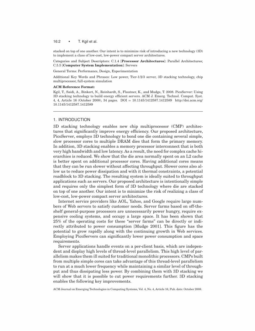
Fig. 1. A diagram depicting the PicoServer: A CMP architecture connected to DRAM using 3D
stacking technology with an on-chip network interface controller (NIC) to provide low-latency,
high-bandwidth networking.
—High-Bandwidth Buses between DRAM and L1 Caches that Support MultipleCores: Thousands of Low-Latency Connections with Marginal Area Overheadbetween Dies are Possible. Since the interconnect buses are on chip, we areable to implement wide buses with a relatively lower power budget comparedto interchip implementations.
—Modification in the Memory Hierarchy due to the Integration of Large-Capacity On-Chip DRAM. It is possible to remove the L2 cache and replace itwith more processing cores. The access latency for the on-chip DRAM 1 is alsoreduced because address multiplexing and off-chip I/O pad drivers [Matickand Schuster 2005] are not required.
—Overall Reduction in System Power, Primarily due to the Reduction inCore Clock Frequency. The benefits of 3D stacking stated in items 1 and 2allow us to integrate more cores clocked at a modest frequency (in our work500–1000MHz) on chip while providing high throughput. Reduced core clockfrequency allows their architecture to be simplified; for example, by usingshorter pipelines with reduced forwarding logic.
The potential drawback of 3D stacking, now that the technology has beenshown feasible, is thermal containment. However, this is not a limitation forthe type of simple, low-power cores that we are proposing for the PicoServer,as we show in Section 4.5. In fact, the ITRS projections of Table II predict thatsystems consuming just a few watts do not even require a heat sink.
The general architecture of a PicoServer is shown in Figure 1. For the pur-poses of this study we assume a stack of 5∼9 dies. The connections are by viasthat run perpendicular to the dies. The dimensions for a 3D interconnect viavaries from 1∼3μm with a separation of 1∼6μm. Current commercial offer-ings can support 1,000,000 vias per cm2 [Gupta et al. 2004]. This is far morethan we need for PicoServer. These function as interconnect and thermal pipes.For our studies, we assume that the logic-based components (i.e., the micro-processor cores, the network interface controllers (NICs), and peripherals) areon the bottom layer and conventional capacity-oriented DRAMs occupy the
1We will refer to die that are stacked on the main processor die as “on-chip” because they form a
3D chip.
ACM Journal on Emerging Technologies in Computing Systems, Vol. 4, No. 4, Article 16, Pub. date: October 2008.

16:4 • T. Kgil et al.
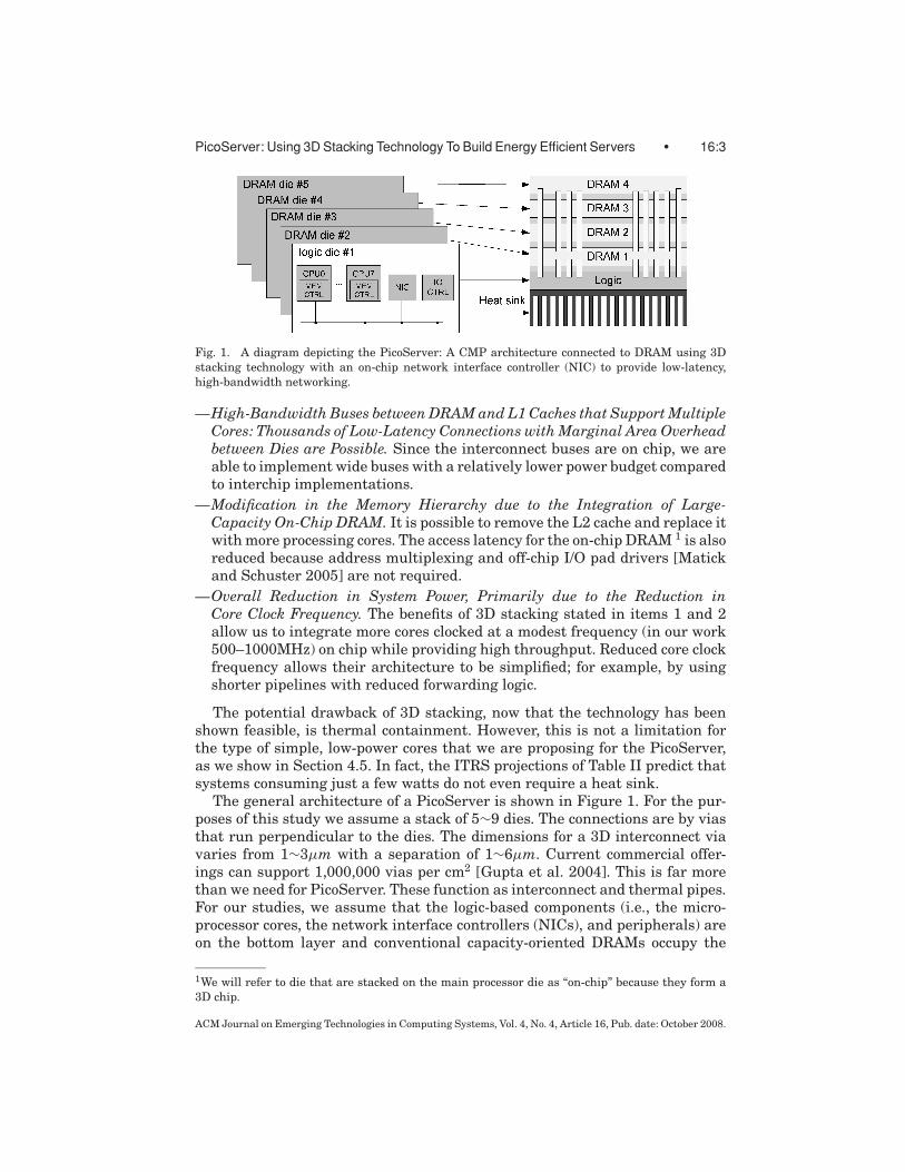
Fig. 2. A typical 3-tier server architecture: tier 1, Web server; tier 2, application server; tier 3,
database server.
remaining layers. To understand the design space and potential benefits of thisnew technology, we explored the trade-offs of different bus widths, numbersof cores, frequencies, and memory hierarchies in our simulations. We foundbus widths of 1024 bits with a latency of 2 clock cycles at 250MHz to be rea-sonable in our architecture. In addition, we aim for a reasonable area budget,constraining the die size area to be below 80mm2 at 90nm process technology.Our 12-core PicoServer configuration, which occupies the largest die area, isconservatively estimated at approximately 80mm2. The die areas for our 4-and 8-core PicoServer configurations are, respectively, 40mm2 and 60mm2.
We also extend our analysis on PicoServer. Specifically, our additional anal-ysis examines three points.
—Analysis on Additional Server Workloads. We expand our scope of serverworkloads to all tiers in a server farm. We show performance and energyefficiency for tier-1, -2, and -3 workloads in the server space (see Figure 2).
—Impact of Multithreading. We show the impact of multithreading on serversleveraging 3D technology. Overall, multithreading improves throughput, butonly to a limited extent when considering the area efficiency. This is because3D technology improves the overall latency to memory, which reduces thebenefits of multithreading.
—Detailed Analysis on System Memory Usage and On-Chip DRAM Architec-ture. We provide a detailed breakdown of system memory usage. Based on theusage behavior, we describe the role of on-chip DRAM. We also describe howthe on-chip DRAM architecture changes using 3D technology. 3D technologyenables us to implement heavily banked system memory architectures thatconsume less power.
The article is organized as follows. In the next section we provide backgroundfor this work by describing an overview of server platforms, 3D stacking tech-nology, and trends in DRAM technology. In Section 3, we outline our methodol-ogy for the design-space exploration. In Section 4, we provide more details forthe PicoServer architecture and evaluate various PicoServer configurations.In Section 5, we present our results in the PicoServer architecture for serverbenchmarks and compare our results to conventional architectures that do not
ACM Journal on Emerging Technologies in Computing Systems, Vol. 4, No. 4, Article 16, Pub. date: October 2008.
PicoServer: Using 3D Stacking Technology To Build Energy Efficient Servers • 16:5
employ 3D stacking. These architectures are CMPs without 3D stacking andconventional high-performance desktop architectures with Pentium 4-like char-acteristics. A summary and concluding remarks are given in Section 6. Muchof the findings we present in this article can also be found in Kgil [2007].
2. BACKGROUND
This section discusses the current state of server platforms, 3D stacking tech-nology, and DRAM technology. We first show how servers are currently deployedin datacenters and analyze the behavior of current server workloads. Next, weexplain the state of 3D stacking technology and how it is applied in this article.Finally, we show advances in DRAM technology. We explain current and futuretrends in DRAM used in the server space.
2.1 Server Platforms
2.1.1 3-Tier Server Architecture. Today’s datacenters are commonly built fol-lowing a 3-tier server architecture. Figure 2 shows a 3-tier server farm and howit might handle a request for service. The first tier handles the bulk of the re-quests from the client. Tier-1 server applications handle events on a per-clientbasis, which are independent and display high levels of thread-level parallelism.Tier-1 servers handle Web requests and forward requests that require heaviercomputation or database accesses to tier 2. Tier-2 servers execute user appli-cations that interpret script languages and determine what objects (typicallydatabase objects) should be accessed. Tier-2 servers generate database requeststo tier-3 servers. Tier-3 servers receive database queries and return the resultsto tier-2 servers.
For example, when a client request comes in for a Java servlet page, it isfirst received by the front-end server: tier 1. Tier 1 recognizes a Java servletpage that must be handled and initiates a request to tier 2, typically usingremote message interfaces (RMIs). Tier 2 initiates a database query on thetier-3 servers, which in turn generate the results and send the relevant infor-mation up the chain, all the way to tier 1. Finally, tier 1 sends the generatedcontent to the client.
Three tier server architectures are commonly deployed in today’s serverfarms, because this allows each level to be optimized for its workload. How-ever, this strategy is not always adopted. Google employs essentially the samemachines at each level, because economies of scale and manageability issuescan outweigh the advantages. We will show that, apart from the database disksystem in the third tier, the generic PicoServer architecture is suitable for alltiers.
2.1.2 Server Workload Characteristics. This section describes the indi-vidual workload behavior of applications commonly found in server farms.Server workloads display a high degree of thread-level parallelism (TLP), sinceconnection-level parallelism through client connections can be easily translatedinto thread-level parallelism (TLP). Table I shows the behavior of commercialserver workloads. Most of the commercial workloads display high TLP and
ACM Journal on Emerging Technologies in Computing Systems, Vol. 4, No. 4, Article 16, Pub. date: October 2008.

16:6 • T. Kgil et al.
Table I. Behavior of Commercial Workloads (adapted from Kunkel et al. [2000])
JBOB SAP3T
Attribute Web99 (JBB) TPC-C SAP 2T DB TPC-H
Application Web Server OLTP ∗ ERP† ERP† DSS‡
Category Server Java
Instruction Level Parallelism low low low med low high
Thread Level Parallelism high high high high high high
Instruction/Data working-set large large large med large large
Data Sharing low med high med high med
I/O Bandwidth high low high med high med
(network) (disk) (disk) (disk) (disk)
∗OLTP : Online Transaction Processing.†ERP : Enterprise Resource Planning.‡DSS : Decision Support System.
low instruction-level parallelism (ILP), with the exception of decision supportsystems. Conventional general-purpose processors, however, are typically op-timized to exploit ILP. These workloads suffer a high cache-miss rate, regu-larly stalling the machine. This leads to low instructions per cycle (IPC) andpoor utilization of processor resources. Our studies have shown that, except forcomputation-intensive workloads like PHP application servers, video stream-ing servers, and decision support systems, out-of-order processors have an IPCbetween 0.21∼0.54 for typical server workloads (i.e., at best, modest compu-tation loads with an L2 cache of 2MB). These workloads do not perform wellbecause much of the requested data has been recently DMAed from the disk tosystem memory, invalidating cached data and leading to cache misses. There-fore, we can generally say that single-thread optimized out-of-order processorsdo not perform well on server workloads. Another interesting property of mostserver workloads is the significant amount of time spent in kernel code, unlikeSPECCPU benchmarks. This kernel code is largely involved in interrupt han-dling for the NIC or disk driver, packet transmission, network stack processing,and disk cache processing.
Finally, a large portion of requests are centered around the same group offiles. These file accesses translate into memory and I/O accesses. Due to themodest computation, memory and I/O latency are critical to high performance.Therefore, disk caching in the system memory plays a critical part in providingsufficient throughput. Without a disk cache, the performance degradation dueto the hard disk drive latency would be unacceptable.
To perform well on these classes of workloads, an architecture should natu-rallly support multiple threads to respond to independent requests from clients.Thus, intuition suggests that a CMP or SMT architecture should be able to bet-ter utilize the processor die area.
2.1.3 Conventional Server Power Breakdown. Figure 3 shows the powerbreakdown of a server platform available today. This server uses a chip mul-tiprocessor implemented with many simple in-order cores to reduce powerconsumption. The power breakdown shows that one-fourth is consumed bythe processor, one-fourth is consumed by the system memory, one-fourth is
ACM Journal on Emerging Technologies in Computing Systems, Vol. 4, No. 4, Article 16, Pub. date: October 2008.

PicoServer: Using 3D Stacking Technology To Build Energy Efficient Servers • 16:7
Fig. 3. Power breakdown of T2000 UltraSPARC executing SpecJBB.
consumed by the power supply, and one-fifth is consumed by the I/O interface.Immediately we can see that using a relatively large amount of system memoryresults in the consumption of a substantial fraction of power. This is expected toincrease as the system memory clock frequency increases and system memorycapacity increases. We also find that despite using simpler cores that are energyefficient, a processor would still consume a noticeable amount of power. The I/Ointerface consumes a large amount of power due to the high I/O supply voltagerequired in off-chip interfaces. The I/O supply voltage is likely to reduce as wescale in the future, but won’t scale as much as the core supply voltage. Thissuggests that system-level integration could further reduce power. Finally, wefind that the power supply displays some inefficiency. This is due to the multiplelevels of voltage it has to support. In summary, 3D stacking technology has thepotential to reduce the power consumed by the processor and the I/O interfacesby pushing system integration to the next level.
2.2 3D Stacking Technology
This section provides an overview of 3D stacking technology. In the past therehave been numerous efforts in academia and industry to implement 3D stackingtechnology [Black et al. 2004; Lee et al. 2000; Koyanagi 2005; Lu 2005; Xue et al.2003]. They have met with mixed success. This is due to the many challengesthat need to be addressed, including (1) achieving high yield in bonding diestacks, (2) delivering power to each stack, and (3) managing thermal hotspotsdue to stacking multiple dies. However, in the past few years strong marketforces in the mobile terminal space have accelerated a demand for small formfactors with very low power. In response, several commercial enterprizes havebegun offering reliable low-cost die-to-die 3D stacking technologies.
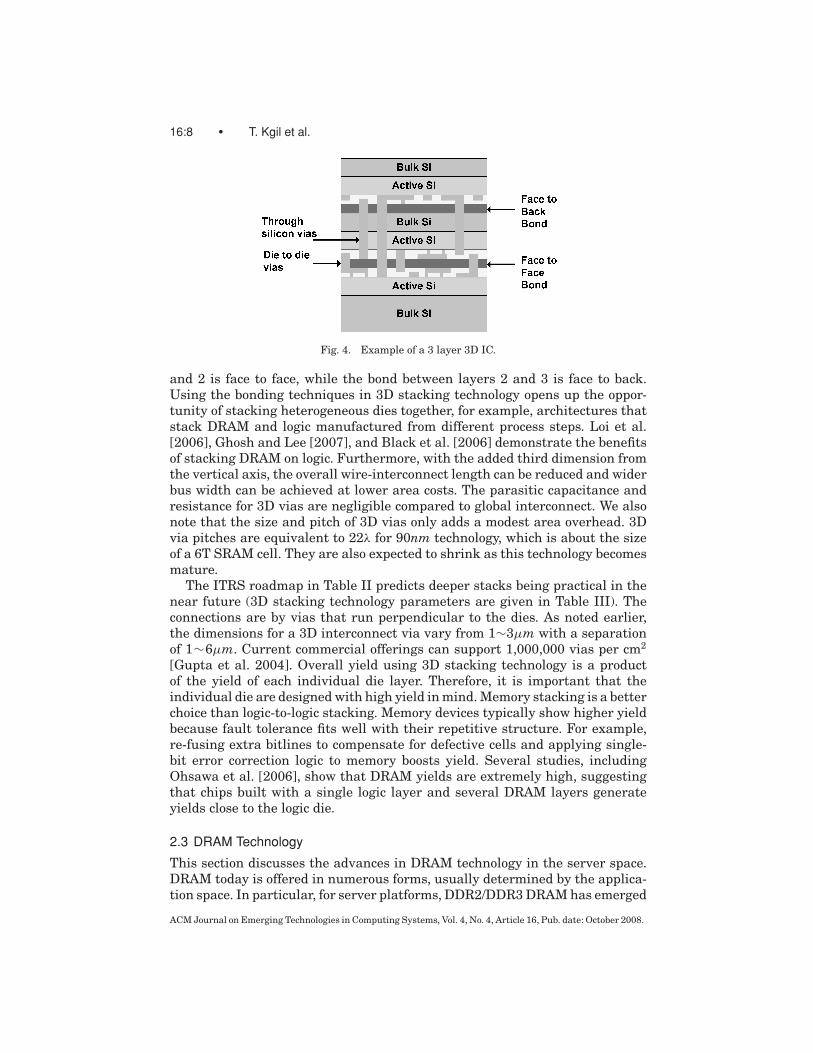
In 3D stacking technology, dies are typically bonded as face to face or face toback. Face-to-face bonds provide higher die-to-die via density and lower areaoverhead than face-to-back bonds. The lower via density for face-to-back bondsresults from the through-silicon vias (TSVs) that have to go through siliconbulk. Figure 4 shows a high-level example of how dies can be bonded using3D stacking technology. The bond between layers 1 (starting from the bottom)
ACM Journal on Emerging Technologies in Computing Systems, Vol. 4, No. 4, Article 16, Pub. date: October 2008.
16:8 • T. Kgil et al.
Fig. 4. Example of a 3 layer 3D IC.
and 2 is face to face, while the bond between layers 2 and 3 is face to back.Using the bonding techniques in 3D stacking technology opens up the oppor-tunity of stacking heterogeneous dies together, for example, architectures thatstack DRAM and logic manufactured from different process steps. Loi et al.[2006], Ghosh and Lee [2007], and Black et al. [2006] demonstrate the benefitsof stacking DRAM on logic. Furthermore, with the added third dimension fromthe vertical axis, the overall wire-interconnect length can be reduced and widerbus width can be achieved at lower area costs. The parasitic capacitance andresistance for 3D vias are negligible compared to global interconnect. We alsonote that the size and pitch of 3D vias only adds a modest area overhead. 3Dvia pitches are equivalent to 22λ for 90nm technology, which is about the sizeof a 6T SRAM cell. They are also expected to shrink as this technology becomesmature.
The ITRS roadmap in Table II predicts deeper stacks being practical in thenear future (3D stacking technology parameters are given in Table III). Theconnections are by vias that run perpendicular to the dies. As noted earlier,the dimensions for a 3D interconnect via vary from 1∼3μm with a separationof 1∼6μm. Current commercial offerings can support 1,000,000 vias per cm2
[Gupta et al. 2004]. Overall yield using 3D stacking technology is a productof the yield of each individual die layer. Therefore, it is important that theindividual die are designed with high yield in mind. Memory stacking is a betterchoice than logic-to-logic stacking. Memory devices typically show higher yieldbecause fault tolerance fits well with their repetitive structure. For example,re-fusing extra bitlines to compensate for defective cells and applying single-bit error correction logic to memory boosts yield. Several studies, includingOhsawa et al. [2006], show that DRAM yields are extremely high, suggestingthat chips built with a single logic layer and several DRAM layers generateyields close to the logic die.
2.3 DRAM Technology
This section discusses the advances in DRAM technology in the server space.DRAM today is offered in numerous forms, usually determined by the applica-tion space. In particular, for server platforms, DDR2/DDR3 DRAM has emerged
ACM Journal on Emerging Technologies in Computing Systems, Vol. 4, No. 4, Article 16, Pub. date: October 2008.

PicoServer: Using 3D Stacking Technology To Build Energy Efficient Servers • 16:9
Table II. ITRS Projection [ITRS 2005] for 3D Stacking Technology, Memory Array Cells
and Maximum Power Budget for Power-Aware Platforms
2007 2009 2011 2013 2015
Low-cost/handheld #die/stack 7 9 11 13 14
SRAM density Mbits/cm2 138 225 365 589 948
DRAM density Mbits/cm2 at production 1,940 3,660 5,820 9,230 14,650
Max. Power Budget for
cost-performance systems(W) 104 116 119 137 137
Max. Power Budget for low-cost/handheld
systems with battery(W) 3.0 3.0 3.0 3.0 3.0
ITRS projections suggest DRAM density exceeds SRAM density by 15∼18×, entailing large capacity of
DRAM can be integrated on chip using 3D stacking technology as compared to SRAM.
Table III. 3D Stacking Technology Parameters [Gupta et al. 2004; Banerjee et al. 2001; Lu 2005]
Face-to-Back Face-to-Face RPI MIT 3D FPGA
Size 1.2μ × 1.2μ 1.7μ × 1.7μ 2μ × 2μ 1μ × 1μ
Minimum Pitch <4μ 2.4μ N/A N/A
Feed Through Capacitance 2∼3fF ≈0 N/A 2.7fF
Series Resistance <0.35� ≈0 ≈0 ≈0
as the primary solution for system memory. FBDIMM DRAM that delivershigher throughput than DDR2/DDR3 is emerging as an alternative, but higherpower, solution. RLDRAM and NetRAM [NetRAM 2005; RLDRAM 2008] arealso popular DRAM choices for network workloads in the server space. Thecommon properties for these memories are high throughput and low latency.In the server space, DRAM must meet the high-throughput and low-latencydemands to deliver high performance. These demands can only be achievedat the price of increasing power consumption in the DRAM I/O interface andthe DRAM arrays. As a result, power has increased to a point where the I/Opower and DRAM power contribute to a significant amount of overall systempower (as we showed in Section 2.1.3). Industry has addressed this concernby reducing the I/O supply voltage and introducing low-power versions of theDDR2 interface at the price of sacrificing both throughput and latency. We willshow that DRAM stacked using 3D stacking technology can be implementedto deliver high-throughput and low-latency DRAM interfaces while consumingmuch less power.
3. METHODOLOGY
To explore the design space for 3D stacking technology, we modeled the benefitsgained using 3D technology on a full-system simulator. The architectural as-pects of our studies were obtained from a microarchitectural simulator calledM5 [Binkert et al. 2006] that is able to run Linux and evaluate full system-level performance. We model multiple servers connected to multiple clients inM5. The client requests are generated from user-level network application pro-grams. We measure server throughput (network bandwidth or transactions persecond) to estimate performance. We also estimated die area size based on previ-ous publications and developed models for delay and power. They were derived
ACM Journal on Emerging Technologies in Computing Systems, Vol. 4, No. 4, Article 16, Pub. date: October 2008.

16:10 • T. Kgil et al.
from data published by industry and academia [ITRS 2005; Gupta et al. 2004;Rahman and Reif 2000; 3DRISC 2004; Banerjee et al. 2001; Black et al. 2004].DRAM timing- and power values were obtained from IBM and Micron technol-ogy datasheets [MicronDRAM 2008]. A detailed description of our methodologyis described in the following subsections.
3.1 Simulation Studies
3.1.1 Full-System Architectural Simulator. To evaluate the performance ofour server we used the M5 full-system simulator. M5 boots an unmodified Linuxkernel on a configurable architecture. Multiple systems are created in the sim-ulator to model the clients and servers, and connected via an ethernet linkmodel. The server side executes Apache (a Web server), Fenice (a video stream-ing server), MySQL (a database server), and NFS (a file server). The client sideexecutes benchmarks that generate representative requests for dynamic andstatic Web page content, video stream requests, database queries, and networkfile commands, respectively. For comparison purposes we defined a Pentium4-like system [Schutz and Webb 2004], and a chip multiprocessor-like systemsimilar to Kongetira et al. [2005]. We also looked at several configurations using3D stacking technology on these platforms. We assume that with 3D stackingtechnology, wider bus widths can be implemented with lower power overhead.Table IV shows the configurations used in our simulations.
3.1.2 Server Benchmarks. We use several benchmarks that directly in-teract with client requests. We used two Web-content-handling benchmarks,SURGE [Barford and Crovella 1998] and SPECweb99 [SPECWeb 1999] to mea-sure Web server performance. Both benchmarks request filesets of more than1GB. A Web-script-handling benchmark, SPECweb2005 [SPECWeb 2005], us-ing PHP is selected to represent script workloads. A video streaming bench-mark, Fenice [LS3 2007], which uses the RTSP protocol along with the UDPprotocol, is chosen to measure behavior for on-demand workloads. For a file-sharing benchmark we use an NFS server and stress it with dbench. Finally,we execute two database benchmarks to measure database performance fortier-2 and -3 workloads.
SURGE. The SURGE benchmark represents client requests for static Webcontent. We modified the SURGE fileset and used a zipf distribution to generatereasonable client requests. Based on the zipf distribution, a static Web pagewhich is approximately 12KB in file size is requested 50% of the time in ourclient requests. We configured the SURGE client to have 20 outstanding clientrequests.
SPECweb99. To evaluate a mixture of static Web content and simple dynamicWeb content, we used a modified version of SURGE to request SPECweb99filesets (behavior illustrated in Table I). We used the default configuration forSPECweb99 to generate client requests. Specifically, 70% of client requests arefor static Web content and 30% are for dynamic Web content.
SPECweb2005. Scripting languages are a popular way to describe Web pages.SPECweb2005 offers three types of benchmarks: a banking benchmark that
ACM Journal on Emerging Technologies in Computing Systems, Vol. 4, No. 4, Article 16, Pub. date: October 2008.

PicoServer: Using 3D Stacking Technology To Build Energy Efficient Servers • 16:11
Ta
ble
IV.
Com
mon
lyU
sed
Sim
ula
tion
Con
figu
rati
on
s
OO
4-s
ma
llb
ase
lin
eO
O4
-la
rge
ba
seli
ne
Con
ven
tion
al
CM
PP
icoM
P4
/8/1
2-5
00
MH
z/
/w
.3
Dst
ack
ing
/w
.3
Dst
ack
ing
MP
4/8
w.o
.3
Dst
ack
ing
10
00
MH
z∗
Op
era
tin
gF
req
uen
cy4
GH
z4
GH
z1
GH
z5
00
MH
z/1
GH
z
Nu
mb
er
of
Pro
cess
ors
11
4/8
4/8
/12
Pro
cess
or
Typ
eou
t-of-
ord
er
ou
t-of-
ord
er
in-o
rder
in-o
rder
Issu
eW
idth
44
11
L1
cach
e2
way
16
KB
2w
ay
12
8K
B4
way
16
KB
per
core
4w
ay
16
KB
per
core
L2
cach
e8
way
25
6K
B7
.5n
s8
way
2M
B7
.5n
s8
way
2M
B1
6n
s
un
loa
ded
late
ncy
un
loa
ded
late
ncy
un
loa
ded
late
ncy
N/A
Mem
ory
bu
sw
idth
64
bit
@4
00
MH
z/6
4b
it@
40
0M
Hz/
64
bit
@2
50
MH
z1
02
4b
it@
25
0M
Hz
10
24
bit
@2
50
MH
z1
02
4b
it@
25
0M
Hz
Syst
em
Mem
ory
51
2M
BD
DR
25
12
MB
DD
R2
51
2M
BD
DR
21
28
MB
∼51
2M
B
DR
AM
DR
AM
DR
AM
DD
R2
DR
AM
∗ Pic
oS
erv
er
pla
tform
usi
ng
3D
sta
ckin
gte
chn
olo
gy.
Th
eco
recl
ock
freq
uen
cyof
Pic
oS
erv
er
isty
pic
all
y5
00
MH
z.P
icoS
erv
er
con
figu
rati
on
sw
ith
1G
Hz
core
clock
freq
uen
cy
are
late
ru
sed
tosh
ow
the
imp
act
of
3D
sta
ckin
gte
chn
olo
gy.
Syst
em
mem
ory
late
nci
es
are
gen
era
ted
from
DD
R2
DR
AM
mod
els
.W
ea
ssu
me
core
scl
ock
ed
at
low
er
clock
freq
uen
cies
(belo
w1
GH
z)h
ave
hig
her
L1
cach
ea
ssoci
ati
vit
y.
L2
cach
eu
nlo
ad
ed
late
ncy
for
sin
gle
-core
an
dm
ult
icore
con
figu
rati
on
sd
iffe
rd
ue
tolo
nger
glo
ba
lin
terc
on
nect
len
gth
sin
mu
ltic
ore
pla
tform
s[L
au
don
20
05
].
ACM Journal on Emerging Technologies in Computing Systems, Vol. 4, No. 4, Article 16, Pub. date: October 2008.
16:12 • T. Kgil et al.
emulates the online banking activity of a user; an e-commerce benchmark thatemulates the online purchase activity; and a support benchmark that emulatesthe online stream activity. All benchmarks require a dynamic Web page tobe generated from a script interpreter. We use a PHP interpreter to measurethe behavior of tier-2 servers. The client requests are generated from methodsdescribed for SPECweb99 and SURGE clients.
Fenice. On-demand video serving is also an important workload for tier-1servers. For copyright protection and live broadcasts, the RTSP protocol is com-monly used for real-time video playback. Fenice is an open-source streamingproject [LS3 2007] that provides workloads supporting the RTSP protocol. Wemodified it to support multithreading. Client requests were generated with amodified version of nemesi, an RTSP-supporting MPEG player. Nemesi is alsofrom the open-source streaming project. We generated multiple client requeststhat fully utilized the server CPUs for a high-quality 16Mbps datastream of720 × 480-resolution MPEG2 frames.
dbench. This benchmark is commonly used to stress NFS daemons. In ourtests we used the in-kernel NFS daemon which is multithreaded and availablein standard Linux kernels. We generated NFS traffic using dbench on the clientside that stressed the file server. Dbench generates workloads that both readand write to the file server while locking these files so that a different clientcannot access it simultaneously.
OLTP. Online transaction processing is a typical workload executed on tier-2and -3 servers (behavior illustrated in Table I). The TPC council has describedin detail benchmarks for OLTP. We used a modified version of TPC-C madeavailable by the Open Source Development Lab (OSDL), called DBT2 [OSDL2006]. DBT2 generates transaction orders. Our database server is MySQL 5.0.We use the InnoDB storage engine that supports transactions and provides areasonable amount of scalability for multicores. We generated a 1GB warehousewhich is typically used for small-scale computation-intensive databases. Wechose a small working-set size due to limitation in simulation time. We selecteda buffer pool size accordingly.
DSS. Decision Support System is another typical workload used to evaluatetier-2 and -3 servers. We used TPC-H, the current version of a DSS workload.Again, a modified version of TPC-H available by OSDL (DBT3) [OSDL 2006] isused in this study. We loaded the TPC-H database onto MySQL and used thedefined TPC-H queries to measure performance. The query cache is disabledto prevent speedup in query time due to caching. To reasonably reduce oursimulation time, we only performed and measured the time for a Q22 queryout of the many TPC-H queries. A Q22 query takes a modest amount of time toexecute and displays the behaviors illustrated in Table I.
3.2 Estimating Power and Area
Power and area estimation at the architectural level is difficult to do withgreat accuracy. To make a reasonable estimation and show general trends, we
ACM Journal on Emerging Technologies in Computing Systems, Vol. 4, No. 4, Article 16, Pub. date: October 2008.

PicoServer: Using 3D Stacking Technology To Build Energy Efficient Servers • 16:13
Table V. Published Power Consumption Values for Various Microprocessors [Clark et al. 2001;
ARM11MPcore 2004; Ricci et al. 2005; Schutz and Webb 2004]
Pentium 4 90nm ARM11 130nm Xscale 90nm∗ PicoServer MP 90nm†
L1 cache 16KB 16KB 32KB 16KB
L2 cache 1MB N/A N/A N/A
Total Power(W) 89–103W 250mW @ 850mW @ 190mW @
550MHz 1.5GHz 500MHz
Total Die Area(mm2) 112 5–6 6–7 4–5
∗Die area for a 90nm Xscale excludes L2 cache [Ricci et al. 2005].†For the PicoServer core, we estimated our power to be in the range of an ARM11, Xscale.
resorted to industry white papers, datasheets, and academia publications ondie area, and we compared our initial analytical power models with real imple-mentations and widely used cycle-level simulation techniques. We discuss thisfurther in the next subsections.
3.2.1 Processors. We relied to a large extent on the figures reported inClark et al. [2001], ARM11MPcore [2004], and Ricci et al. [2005] for an ARMprocessor to estimate processor power and die area. The ARM is represen-tative of a simple in-order 32-bit processor that would be suitable for thePicoServer. Due to the architectural similarities with our PicoServer cores, weextrapolated the die area and power consumption for our PicoServer cores at500MHz from published data in Clark et al. [2001], ARM11MPcore [2004], andRicci et al. [2005]. Table V lists these estimates, along with values listed inARM11MPcore [2004], and Ricci et al. [2005] and a Pentium 4 core for compari-son. A die area analysis on the expected die area per core was also conducted. Wecollected several die area numbers available from ARM, MIPS, PowerPC, andother comparable scalar in-order processors. We also synthesized several 32-bitopen-source cores that are computationally comparable to a single PicoServercore. We synthesized them using the Synopsys Physical compiler toolset.
The power values listed in Table V include static power. Our estimates fora 500MHz PicoServer core are conservative compared to the ARM core values,especially with respect to Ricci et al. [2005]. Given that the Xscale core con-sumes 850mW at 1.5GHz and 1.3V, a power consumption of 190mW at 500MHzfor the 90nm PicoServer core is conservative when applying the 3× scaling inclock frequency and the additional opportunities to scale voltage. For powerconsumption at other core clock frequencies, for example, 1GHz, we generateda power-versus-frequency plot. It follows a cubic law [Flynn and Hung 2004].We assumed a logic depth of 24 FO4 (fan out of 4) logic gates and used the 90nmPTM process technology [Ricci et al. 2005].
Support for 64 bits in a PicoServer core seems inevitable in the future. We ex-pect the additional area and power overhead for 64-bit support in a PicoServercore to be modest when we look at the additional area and power overheadfor 64-bit support in commercially available cores like MIPS and Xeon. Asfor the L2 cache, we referred to Wendell et al. [2004] and scaled the areaand power numbers generated from actual measurements. We assumed thepower numbers in Wendell et al. [2004] were generated when the cache-accessrate was 100%. Therefore, we scaled the L2 cache power by size and access
ACM Journal on Emerging Technologies in Computing Systems, Vol. 4, No. 4, Article 16, Pub. date: October 2008.
16:14 • T. Kgil et al.
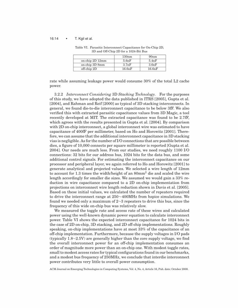
Table VI. Parasitic Interconnect Capacitance for On-Chip 2D,
3D and Off-Chip 2D for a 1024-Bit Bus
130nm 90nm
on-chip 2D 12mm 5.6nF 5.4nF
on-chip 3D 8mm 3.7nF 3.6nF
off-chip 2D 16.6nF 16.6nF
rate while assuming leakage power would consume 30% of the total L2 cachepower.
3.2.2 Interconnect Considering 3D Stacking Technology. For the purposesof this study, we have adopted the data published in ITRS [2005], Gupta et al.[2004], and Rahman and Reif [2000] as typical of 3D stacking interconnects. Ingeneral, we found die-to-die interconnect capacitance to be below 3fF. We alsoverified this with extracted parasitic capacitance values from 3D Magic, a toolrecently developed at MIT. The extracted capacitance was found to be 2.7fF,which agrees with the results presented in Gupta et al. [2004]. By comparisonwith 2D on-chip interconnect, a global interconnect wire was estimated to havecapacitance of 400fF per millimeter, based on Ho and Horowitz [2001]. There-fore, we can assume that the additional interconnect capacitance in 3D stackingvias is negligible. As for the number of I/O connections that are possible betweendies, a figure of 10,000 connects per square millimeter is reported [Gupta et al.2004]. Our needs are much less. From our studies, we need roughly 1100 I/Oconnections: 32 bits for our address bus, 1024 bits for the data bus, and someadditional control signals. For estimating the interconnect capacitance on ourprocessor and peripheral layer, we again referred to Ho and Horowitz [2001] togenerate analytical and projected values. We selected a wire length of 12mmto account for 1.3 times the width/height of an 80mm2 die and scaled the wirelength accordingly for smaller die sizes. We assumed we would gain a 33% re-duction in wire capacitance compared to a 2D on-chip implementation fromprojections on interconnect wire length reduction shown in Davis et al. [2005].Based on these initial values, we calculated the number of repeaters requiredto drive the interconnect range at 250∼400MHz from hspice simulations. Wefound we needed only a maximum of 2∼3 repeaters to drive this bus, since thefrequency of this wide on-chip bus was relatively slow.
We measured the toggle rate and access rate of these wires and calculatedpower using the well-known dynamic power equation to calculate interconnectpower. Table VI shows the expected interconnect capacitance for 1024 bits inthe case of 2D on-chip, 3D stacking, and 2D off-chip implementations. Roughlyspeaking, on-chip implementations have at most 33% of the capacitance of anoff-chip implementation. Furthermore, because the supply voltages in I/O pads(typically 1.8∼2.5V) are generally higher than the core supply voltage, we findthe overall interconnect power for an off-chip implementation consumes anorder of magnitude more power than an on-chip one. With modest toggle rates,small to modest access rates for typical configurations found in our benchmarks,and a modest bus frequency of 250MHz, we conclude that interdie interconnectpower contributes very little to overall power consumption.
ACM Journal on Emerging Technologies in Computing Systems, Vol. 4, No. 4, Article 16, Pub. date: October 2008.
PicoServer: Using 3D Stacking Technology To Build Energy Efficient Servers • 16:15
Table VII. Bandwidth and Latency
DDR2 XDR L2 Cache On-chip
SDRAM DRAM DRAM @1.2GHz DRAM 3D IC
Bandwidth (GB/sec) 1.0 5.2 31.3 21.9 31.3
Average access latency(ns) 30ns 25ns 28ns 16ns 25ns∗
∗Average access latency with no 3D stacking aware optimizations. On-chip DRAM latency expected to
reduce by more than 50% [Matick and Schuster 2005] when 3D stacking optimizations are applied.
These results suggest on-chip DRAM can easily provide enough memory bandwidth compared to an L2
cache, as noted in Laudon [2005] and Wendell et al. [2004]. Average access latency for SDRAM and DDR2
DRAM is estimated to be tRCD+tCAS , where tRCD denotes RAS to CAS delay and tCAS denotes CAS delay.
For, XDRAM tR AC−R is used, where tR AC−R denotes the read-access time.
3.2.3 DRAM. We made DRAM area estimates for the PicoServer using thedata in MacGillivray [2005]. Currently, it is reasonable to say that 80mm2 ofchip area is required for 64MB of DRAM in 90nm technology.
Conventional DRAM is packaged separately from the processor and is ac-cessed through I/O pad pins and wires on a PCB. However, for our architecture,DRAM exists on chip and connects to the processor and peripherals through a3D stacking via. Therefore, the pad power consumed by the packages, necessaryfor driving signals off-chip across the PCB, is avoided in our design. Using theMicron DRAM spreadsheet calculator [MicronDRAM 2008] modified to omitpad power, and profile data from M5 including the number of cycles spent onDRAM reads, writes, and page-hit rates, we generated an average power forDRAM. We compared the estimated power from references on DRAM and espe-cially with the DRAM power values generated from the SunFire T2000 ServerPower Calculator [Sun Fire T2000 2008]. The Micron spreadsheet uses actualcurrent measurements for each DRAM operation: read, write, refresh, bankprecharge, etc. We assumed a design with a 1.8V voltage supply.
3.2.4 Network Interface Controller (NIC). Network interface controllerpower was difficult to model analytically, due to lack of information of thedetailed architecture of commercial NICs. For our simulations, we looked atthe National Semiconductor 82830 gigabit ethernet controller. This chip im-plements the MAC layer of the ethernet card and interfaces, with the physicallayer (PHY) using the gigabit media independent interface (GMII) interface. Weanalyzed the datasheet and found the maximum power consumed by this chipto be 743mW [NSNIC 2001]. This power number is for 180nm technology. Weassumed maximum power is consumed when all the input and output pins areactive.We then derated this figure based on our measured usage. In addition,we assumed static power at 30% of the maximum chip power.
4. PICOSERVER ARCHITECTURE
Table VII shows the latency and bandwidth achieved for conventional DRAM,XDR DRAM, L2 cache, and on-chip DRAM using 3D stacking technology. With a1024-bit wide bus, the memory latency and bandwidth achieved in a 3D stackingon-chip DRAM is comparable to an L2 cache and XDR DRAM. This suggests anL2 cache is not needed if stacking is used. Furthermore, the removal of off-chipdrivers in conventional DRAM reduces access latency by more than 50% [Matick
ACM Journal on Emerging Technologies in Computing Systems, Vol. 4, No. 4, Article 16, Pub. date: October 2008.

16:16 • T. Kgil et al.
and Schuster 2005]. This strengthens our argument that on-chip DRAM canbe as effective as an L2 cache. Another example that strengthens our case isthat DRAM vendors are producing and promoting DRAM implementations withreduced random-access latency [NetRAM 2005; RLDRAM 2008]. Therefore, ourPicoServer architecture does not have an L2 cache and the on-chip DRAM isconnected through a shared-bus architecture to the L1 caches of each core. Therole of this on-chip DRAM is as a primary system memory.
The PicoServer architecture is comprised of single issue in-order processorsthat together create a chip multiprocessor which is a natural match to appli-cations with a high level of TLP [Kongetira et al. 2005]. Each PicoServer CPUcore is clocked at a nominal value of 500MHz and has an instruction and datacache, with the data caches using a MESI cache-coherence protocol. Our stud-ies showed the majority of bus traffic is generated from cache miss traffic, notcache coherence. This is due to the properties of the target application space andthe small L1 caches: 16KB instruction and 16KB data per core. With currentdensities, the capacity of the on-chip DRAM stack in PicoServer is hundredsof megabytes. In the near future this will rise to several gigabytes, as noted inthe Table II. Other components such as the network interface controller (NIC),DMA controller, and additional peripherals that are required in implementinga full system are integrated on the CPU die.
4.1 Core Architecture and the Impact of Multithreading
PicoServer is made up of simple, single issue in-order cores with a five-stagepipeline. A 32-bit architecture is assumed for each core. Branch prediction isstill useful in a server workload. Each core has a hybrid branch predictor witha 1KB history table. Our studies showed the accuracy of the branch predictorfor server workloads to be about 95%.
Each core also includes architectural support for a shared memory protocoland a memory controller that is directly connected to DRAM. The memorycontroller responds to shared bus snoops and cache misses. On a request toDRAM, the memory controller delivers the address, as well as data for memorywrites or the CPU ID for memory reads. The CPU ID is needed for returnrouting of read data. Our estimated die area for a single core is 4∼5mm2 (shownin Table V).
Despite some benefits that can be obtained from multithreading (describedin later paragraphs), we assume no support for multithreading due to the lim-itation in our simulation environment. Without significant modification to acommodity Linux kernel, it is difficult to scale server applications to more than16 cores or threads. For this reason our study of multithreading examined asingle core with multiple threads. We extrapolated this to the multicore corecase to show how many threads would be optimal when we leverage 3D stackingtechnology. Multithreading has the potential to improve overall throughput byswitching thread contexts during lengthy stalls to memory.
To study the impact of multithreading in PicoServer, we assume multithread-ing support that includes an entire thread context: register file, store buffer,and interrupt trap unit. An additional pipeline stage is required to schedule
ACM Journal on Emerging Technologies in Computing Systems, Vol. 4, No. 4, Article 16, Pub. date: October 2008.
PicoServer: Using 3D Stacking Technology To Build Energy Efficient Servers • 16:17
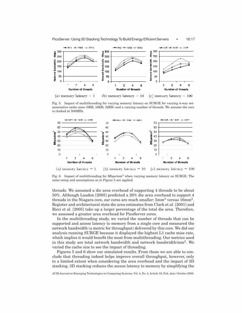
Fig. 5. Impact of multithreading for varying memory latency on SURGE for varying 4-way set-
associative cache sizes (8KB, 16KB, 32KB) and a varying number of threads. We assume the core
is clocked at 500MHz.
Fig. 6. Impact of multithreading for Mbps/mm2 when varying memory latency on SURGE. The
same setup and assumptions as in Figure 5 are applied.
threads. We assumed a die area overhead of supporting 4 threads to be about50%. Although Laudon [2005] predicted a 20% die area overhead to support 4threads in the Niagara core, our cores are much smaller: 5mm2 versus 16mm2.Register and architectural state die area estimates from Clark et al. [2001] andRicci et al. [2005] take up a larger percentage of the total die area. Therefore,we assessed a greater area overhead for PicoServer cores.
In the multithreading study, we varied the number of threads that can besupported and access latency to memory from a single core and measured thenetwork bandwidth (a metric for throughput) delivered by this core. We did ouranalysis running SURGE because it displayed the highest L1 cache miss rate,which implies it would benefit the most from multithreading. Our metrics usedin this study are total network bandwidth and network bandwidth/mm2. Wevaried the cache size to see the impact of threading.
Figures 5 and 6 show our simulated results. From these we are able to con-clude that threading indeed helps improve overall throughput, however, onlyto a limited extent when considering the area overhead and the impact of 3Dstacking. 3D stacking reduces the access latency to memory by simplifying the
ACM Journal on Emerging Technologies in Computing Systems, Vol. 4, No. 4, Article 16, Pub. date: October 2008.

16:18 • T. Kgil et al.
Fig. 7. Network performance on SURGE for various shared bus architectures with an L1 cache of
16KB (each for I and D). We assumed a CPU clock frequency of 500MHz for these experiments. Our
bus architecture must be able to handle high bandwidths as the number of processors increases.
core-to-memory interface and reducing the transfer latency. 3D stacked mem-ory can be accessed in tens of cycles, which corresponds to the plots shownin Figures 5(b) and 6(b). The latter plot suggests that if area efficiency andthroughput are taken together, a limitation of only 2 threads appears optimal.We also find that the memory and I/O traffic increases as we add additionalthreads to the core. Therefore, a system must be able to deliver sufficient I/Obandwidth, and memory bandwidth to accommodate the additional threads.Otherwise, threading will be detrimental to overall system throughput.
4.2 Wide Shared-Bus Architecture
PicoServer adopts a wide shared bus architecture that provides high mem-ory bandwidth and fully utilizes the benefits of 3D stacking technology. Ourbus architecture was determined from SURGE runs on M5; we limited it toSURGE because it generates a representative cache miss rate per core on ourbenchmarks. To explore the design space of our bus architecture, we first ransimulations for varying the bus width on a single shared-bus ranging from 128bits–2048 bits. We varied the cacheline size as well to match the bus width(varied it from 16 bytes–256 bytes). Network bandwidth (a metric for through-put) was measured to determine the impact of bus width on the PicoServer.As shown in Figure (7a), a relatively wide data bus is necessary to achievescalable network performance to satisfy the outstanding cache miss requests.This is because of the high bus contention on the shared data bus for highbus traffic that is generated for narrow bus widths, as shown in Figures (7b)and (7c). As we decrease the bus width, the bus traffic increases, resulting ina superlinear increase in latency. Reducing bus utilization implies reduced busarbitration latency, thus improving network bandwidth. Wide bus widths alsohelp speed-up NIC DMA transfers by allowing a large chunk of data be copiedin one transaction. A 1024-bit bus width seems reasonable for our typical Pi-coServer configurations of 4, 8, and 12 cores. Having more cores causes networkperformance to saturate, unless wider buses are employed. We also looked at in-terleaved bus architectures but found that with our given L1 cache miss rates,
ACM Journal on Emerging Technologies in Computing Systems, Vol. 4, No. 4, Article 16, Pub. date: October 2008.

PicoServer: Using 3D Stacking Technology To Build Energy Efficient Servers • 16:19
Table VIII. Projected On-Chip DRAM Size for Varying Process Technologies
130nm 110nm 90nm 80nm
DRAM stack of 4 layers each layer 40mm2 64MB 96MB 128MB 192MB
DRAM stack of 8 layers each layer 40mm2 128MB 192MB 256MB 384MB
DRAM stack of 4 layers each layer 60mm2 96MB 144MB 192MB 288MB
DRAM stack of 8 layers each layer 60mm2 192MB 288MB 384MB 576MB
DRAM stack of 4 layers each layer 80mm2 128MB 192MB 256MB 384MB
DRAM stack of 8 layers each layer 80mm2 256MB 384MB 512MB 768MB
Area estimates are generated based on Semiconductor SourceInsight 2005 [MacGillivray 2005]. 80mm2
of die size is similar to that of a Pentium M at 90nm.
a 1024-bit bus is wide enough to handle the bus requests. For architecturesand workloads that generate higher bus requests as a result of increasing thenumber of cores to 16 or more, or by having L1 caches with higher miss rates(more than 10%), then interleaving the bus becomes more effective. An inter-leaved bus architecture increases the number of outstanding bus requests, thusaddressing the increase in number of bus requests.
4.3 On-Chip DRAM Architecture
4.3.1 Role of On-Chip DRAM. Based on the logic die area estimates, we pro-jected the DRAM die size for a 12-core PicoServer to be 80mm2, and 40mm2
and 60mm2, respectively, for a 4-core and 8-core PicoServer. Table VIII showsthe on-chip memory alternatives for PicoServers. For example, to obtain a totalDRAM size of 256MB, we assume a DRAM made up of a stack of 4 layers. Fortier-3 servers we employ 8 layers because they rely heavily on system memorysize. With current technology, namely 90nm, it is feasible to create a 4-layerstack containing 256MB of physical memory for a die area of 80mm2. Althougha large amount of physical memory is common in server farms (4GB–16GB) to-day, we believe server workloads can be scaled to fit into smaller systems withsmaller physical memory, based on our experience with server workloads anddiscussions with datacenter experts [Lim et al. 2008]. From our measurementson memory usage for server applications shown in Figure 8, we found for manyof the server applications (except TPC-C and TPC-H) that a modest amountof (around 64MB) of system memory is occupied by the user application, data,and the kernel OS code. The remainder of the memory is either free or used asa disk cache. When we consider that much of the user memory space in TPC-Cand TPC-H is allocated as user-level cache, this is even true for TPC-C andTPC-H. Considering the fact that 256MB can be integrated on-chip for 4 dielayers, a large portion of on-chip DRAM can be used as a disk cache. There-fore, for applications that require small/medium filesets, an on-chip DRAM of256MB is enough to handle client requests.
For large filesets, there are several options to choose from. First, we could addadditional on-chip DRAM by stacking additional DRAM dies, as in the 8-layercase. From the ITRS roadmap in Table II, recall that the number of stacked dieswe assume is conservative. With aggressive die stacking, we could add more diestacks to improve on-chip DRAM capacity; ITRS projects more than 11 layersin the next 2∼4 years. This is possible because our power density in the logic
ACM Journal on Emerging Technologies in Computing Systems, Vol. 4, No. 4, Article 16, Pub. date: October 2008.

16:20 • T. Kgil et al.
Fig. 8. Breakdown in memory for server benchmarks (SURGE, SPECweb99, Fenice, dbench,
SPECweb2005, TPC-C). TPC-H is excluded because it displayed similar memory usage as TPC-C.
ACM Journal on Emerging Technologies in Computing Systems, Vol. 4, No. 4, Article 16, Pub. date: October 2008.
PicoServer: Using 3D Stacking Technology To Build Energy Efficient Servers • 16:21
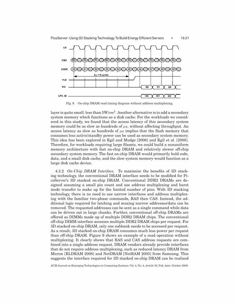
Fig. 9. On-chip DRAM read timing diagram without address multiplexing.
layer is quite small: less than 5W/cm2. Another alternative is to add a secondarysystem memory which functions as a disk cache. For the workloads we consid-ered in this study, we found that the access latency of this secondary systemmemory could be as slow as hundreds of μs, without affecting throughput. Anaccess latency as slow as hundreds of μs implies that the flash memory thatconsumes less active/standby power can be used as secondary system memory.This idea has been explored in Kgil and Mudge [2006] and Kgil et al. [2008].Therefore, for workloads requiring large filesets, we could build a nonuniformmemory architecture with fast on-chip DRAM and relatively slower off-chipsecondary system memory. The fast on-chip DRAM would primarily hold code,data, and a small disk cache, and the slow system memory would function as alarge disk cache device.
4.3.2 On-Chip DRAM Interface. To maximize the benefits of 3D stack-ing technology, the conventional DRAM interface needs to be modified for Pi-coServer’s 3D stacked on-chip DRAM. Conventional DDR2 DRAMs are de-signed assuming a small pin count and use address multiplexing and burstmode transfer to make up for the limited number of pins. With 3D stackingtechnology, there is no need to use narrow interfaces and address multiplex-ing with the familiar two-phase commands, RAS then CAS. Instead, the ad-ditional logic required for latching and muxing narrow addresses/data can beremoved. The requested addresses can be sent as a single command while datacan be driven out in large chunks. Further, conventional off-chip DRAMs areoffered as DIMMs made up of multiple DDR2 DRAM chips. The conventionaloff-chip DIMM interface accesses multiple DDR2 DRAM chips per request. For3D stacked on-chip DRAM, only one subbank needs to be accessed per request.As a result, 3D stacked on-chip DRAM consumes much less power per requestthan off-chip DRAM. Figure 9 shows an example of a read operation withoutmultiplexing. It clearly shows that RAS and CAS address requests are com-bined into a single address request. DRAM vendors already provide interfacesthat do not require address multiplexing, such as reduced latency DRAM fromMicron [RLDRAM 2008] and NetDRAM [NetRAM 2005] from Samsung. Thissuggests the interface required for 3D stacked on-chip DRAM can be realized
ACM Journal on Emerging Technologies in Computing Systems, Vol. 4, No. 4, Article 16, Pub. date: October 2008.

16:22 • T. Kgil et al.
with only minor changes to existing solutions. Additional die area made avail-able through the simplification of the interface can be used to speed-up theaccess latency to on-chip DRAM. By investing more die area to subbank theon-chip DRAM, latencies as low as 10ns can be achieved.2
4.3.3 Impact of On-Chip DRAM Refresh on Throughput. DRAM periodi-cally requires each DRAM cell to be refreshed. Retention time of each DRAM cellis typically defined as 64ms for industry standard temperature and decreasesto 32ms in hotter environments. Based on our thermal analysis presented inSection 4.5, our maximum junction temperature was well under the industrystandard temperature constraints. As a result, we assumed a 64ms refresh cycleper cell. However, refresh circuits are commonly shared among multiple DRAMcell arrays to reduce the die area overhead, reducing the average DRAM refreshinterval to approximately 7.8125μs and requiring approximately 200ns to com-plete. Roughly speaking, this implies that a DRAM bank cannot be accessedfor a duration of hundreds of CPU clock cycles every ten thousands of CPUclock cycles. To measure the impact of refresh cycles, we modeled the refreshactivity of DRAM on M5 and observed the CPI overhead. The access frequencyto on-chip DRAM is directly correlated to the amount of L1 cache misses ob-served. We found that for a 5% L1 cache miss rate and 12 cores clocked at500MHz (PicoMP12-500MHz running SURGE), this would incur a CPI refreshoverhead of 0.03 CPI. This is because many of the L1 cache misses do not occurwhen a refresh command is executed, resulting in only a marginal performancepenalty.
4.4 The Need for Multiple NICs on a CMP Architecture
A common problem of servers with large network pipes is handling burstybehavior in the hundreds of thousands of packets that can arrive each second.Interrupt coalescing is one method of dealing this problem. It works by startinga timer when a noncritical event occurs. Any other noncritical events that occurbefore the timer expires are coalesced into one interrupt, reducing their totalnumber. Even with this technique, however, the number of interrupts receivedby a relatively low-frequency processor, such as one of the PicoServer cores, canoverwhelm it. In our simulations we get around this difficulty by having multi-ple NICs, one for each of a subset of the processors. For an 8-chip multiprocessorarchitecture with 1 NIC and on-chip DRAM, we found the average utilizationper processor to be below 60%, as one processor could not manage the NIC byitself. To fully utilize each processor in our multiple processor architecture, weinserted 1 NIC for every 2 processors. For example, a 4-processor architecturewould have 2 NICs, an 8-processor architecture would have 4 NICs, and soforth.
Although our simulation environment does not support it, a more ideal so-lution would have a smarter single NIC that could route interrupts to multipleCPUs, each with separate DMA descriptors and TX/RX queues. This could be
2In this study, we took a conservative approach and did not apply the latency reduction due to
additional subbanking. We only applied latency optimizations due to the removal of off-chip drivers.
ACM Journal on Emerging Technologies in Computing Systems, Vol. 4, No. 4, Article 16, Pub. date: October 2008.
PicoServer: Using 3D Stacking Technology To Build Energy Efficient Servers • 16:23
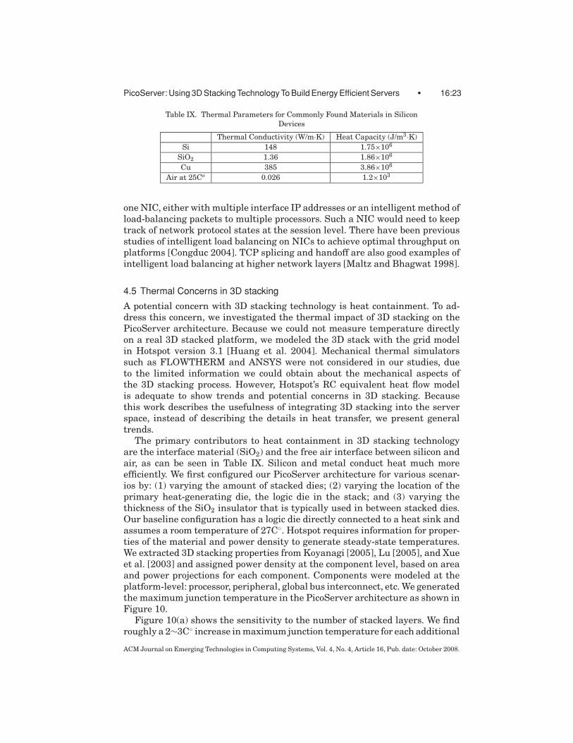
Table IX. Thermal Parameters for Commonly Found Materials in Silicon
Devices
Thermal Conductivity (W/m·K) Heat Capacity (J/m3·K)
Si 148 1.75×10⁶
SiO2 1.36 1.86×10⁶
Cu 385 3.86×10⁶
Air at 25Co 0.026 1.2×10³
one NIC, either with multiple interface IP addresses or an intelligent method ofload-balancing packets to multiple processors. Such a NIC would need to keeptrack of network protocol states at the session level. There have been previousstudies of intelligent load balancing on NICs to achieve optimal throughput onplatforms [Congduc 2004]. TCP splicing and handoff are also good examples ofintelligent load balancing at higher network layers [Maltz and Bhagwat 1998].
4.5 Thermal Concerns in 3D stacking
A potential concern with 3D stacking technology is heat containment. To ad-dress this concern, we investigated the thermal impact of 3D stacking on thePicoServer architecture. Because we could not measure temperature directlyon a real 3D stacked platform, we modeled the 3D stack with the grid modelin Hotspot version 3.1 [Huang et al. 2004]. Mechanical thermal simulatorssuch as FLOWTHERM and ANSYS were not considered in our studies, dueto the limited information we could obtain about the mechanical aspects ofthe 3D stacking process. However, Hotspot’s RC equivalent heat flow modelis adequate to show trends and potential concerns in 3D stacking. Becausethis work describes the usefulness of integrating 3D stacking into the serverspace, instead of describing the details in heat transfer, we present generaltrends.
The primary contributors to heat containment in 3D stacking technologyare the interface material (SiO2) and the free air interface between silicon andair, as can be seen in Table IX. Silicon and metal conduct heat much moreefficiently. We first configured our PicoServer architecture for various scenar-ios by: (1) varying the amount of stacked dies; (2) varying the location of theprimary heat-generating die, the logic die in the stack; and (3) varying thethickness of the SiO2 insulator that is typically used in between stacked dies.Our baseline configuration has a logic die directly connected to a heat sink andassumes a room temperature of 27C◦. Hotspot requires information for proper-ties of the material and power density to generate steady-state temperatures.We extracted 3D stacking properties from Koyanagi [2005], Lu [2005], and Xueet al. [2003] and assigned power density at the component level, based on areaand power projections for each component. Components were modeled at theplatform-level: processor, peripheral, global bus interconnect, etc. We generatedthe maximum junction temperature in the PicoServer architecture as shown inFigure 10.
Figure 10(a) shows the sensitivity to the number of stacked layers. We findroughly a 2∼3C◦ increase in maximum junction temperature for each additional
ACM Journal on Emerging Technologies in Computing Systems, Vol. 4, No. 4, Article 16, Pub. date: October 2008.

16:24 • T. Kgil et al.
Fig. 10. Maximum junction temperature for sensitivity experiments on Hotspot: (a) varying the
number of layers; (b)varying 3D interface thickness; (c)varying location of logic die; (d) maximum
junction temperature for heat sink quality analysis. A core clock frequency of 500MHz is assumed
in calculating power density. We varied the size of on-chip memory based on the number of layers
stacked. 1 layer assumes no on-chip memory at all.
layer stacked. Interestingly, maximum junction temperature reduces as we in-crease the die area. We believe this is due to our floorplan and package as-sumptions. Further analysis is needed, and we leave it for future research.Figure 10(b) shows the sensitivity to the 3D stacking dielectric interface. Wecompared the effect of the SiO2 thickness (the interface material) for 10μm and80μm. In Black et al. [2004], Koyanagi [2005], Lu [2005], and Xue et al. [2003]we find the maximum thickness of the interface material does not exceed 10μmfor 3D stacking. The 80μm point is selected to show the impact of heat contain-ment as the thickness is increased substantially. It results in a 6C◦ increasein junction temperature. While notable, this is not a great change, given thedramatic change in material thickness. We assumed the increase in dielectricinterface thickness did not increase bus latency because the frequency of ouron-chip bus was relatively slow. Figure 10(c) shows the sensitivity to placementin the stack, top or bottom layer. We find the primary heat-generating die is notsensitive to the location of the heat sink.
ACM Journal on Emerging Technologies in Computing Systems, Vol. 4, No. 4, Article 16, Pub. date: October 2008.
PicoServer: Using 3D Stacking Technology To Build Energy Efficient Servers • 16:25
We also conducted an analysis on the impact of heat-sink quality. We variedthe heat sink configuration to model a high-cost heat sink (heat sink 1) and alow-cost heat sink (heat sink 2). Figure 10(d) shows the impact of 3D stackingtechnology on heat-sink quality. It clearly suggests that a low-cost heat sinkcan be used on platforms using 3D stacking technology.
The aforementioned results suggest that heat containment is not a majorlimitation for the PicoServer architecture. The power density is relatively low,not exceeding 5W/cm2. As a result, the maximum junction temperature doesnot exceed 50C◦. 3D vias can also act as heat pipes, which we did not take intoaccount in our analysis; however, this can be expected to improve the situation.An intelligent placement would assign the heat-generating layer (the proces-sor layer) adjacent to the heat sink, resulting in a majority of the heat beingtransferred to the heat sink. There is independent support for our conclusionsin Chiang et al. [2001] and Goplen and Sapatnekar [2005].
5. RESULTS
To evaluate the PicoServer architecture, two metrics are important: throughputand power. Throughput that can be measured as network bandwidth or trans-actions per seconds is a good indicator of overall system performance becauseit is a measure of how many requests were serviced. In this section, we com-pare various PicoServer configurations to other architectures, first in terms ofachievable throughput and then in terms of power. Since the PicoServer has notbeen implemented, we use a combination of analytical models and publisheddata to make a conservative estimate about the power dissipation of variouscomponents. Finally, we present a Pareto chart showing the energy efficiencyof the PicoServer architecture.
5.1 Overall Performance
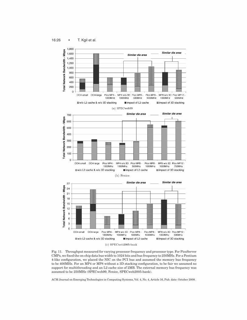
Figures 11 and 12 show the throughput for some of our tier-1, -2, and -3 workloadruns. Each bar shows the contribution to throughput in three parts: (1) a base-line with no L2 cache and a narrow (64-bit) bus; (2) the baseline, but with anL2 cache; or (3) the baseline with a wide bus, no L2 cache, and 3D stacking forDRAM. Hence, we are able to make comparisons that differentiate the impactof 3D stacking technology with the impact of having an L2 cache. Figure 11shows that using 3D stacking technology alone improves overall performanceas much as or more than having an L2 cache. A fair comparison for a fixed num-ber of cores, for example, would be a Pico MP4-1000MHz versus a conventionalCMP MP4 without 3D-1000MHz. In general, workloads that generated modestto high cache miss rates (SURGE, SPECweb99, SPECweb2005, and dbench)showed dramatic improvement from adopting 3D stacking technology. Feniceshows less dramatic improvements, because it involves video stream computa-tions that generate lower cache miss rates. Interestingly, the script languagetier-2 benchmark, SPECweb2005, performed well against OO4 configurationsthat were expressly designed for single-threaded performance.
For OO4 configurations, we combine the impact of having an L2 cache and3D stacking, since the L2 cache latency on a uniprocessor is likely to be smaller
ACM Journal on Emerging Technologies in Computing Systems, Vol. 4, No. 4, Article 16, Pub. date: October 2008.
16:26 • T. Kgil et al.
Fig. 11. Throughput measured for varying processor frequency and processor type. For PicoServer
CMPs, we fixed the on-chip data bus width to 1024 bits and bus frequency to 250MHz. For a Pentium
4-like configuration, we placed the NIC on the PCI bus and assumed the memory bus frequency
to be 400MHz. For an MP4 or MP8 without a 3D stacking configuration, to be fair we assumed no
support for multithreading and an L2 cache size of 2MB. The external memory bus frequency was
assumed to be 250MHz (SPECweb99, Fenice, SPECweb2005-bank).
ACM Journal on Emerging Technologies in Computing Systems, Vol. 4, No. 4, Article 16, Pub. date: October 2008.

PicoServer: Using 3D Stacking Technology To Build Energy Efficient Servers • 16:27
Fig. 12. Throughput measured for varying processor frequency and processor type
(SPECweb2005-ecommerce, dbench,TPC-C). We applied the same assumptions used in Figure 11.
ACM Journal on Emerging Technologies in Computing Systems, Vol. 4, No. 4, Article 16, Pub. date: October 2008.

16:28 • T. Kgil et al.
than the access latency to a large-capacity DRAM, making it less appealingto only have a high-bandwidth on-chip DRAM implemented from 3D stacking.We find that 3D stacking improves performance by 15% on OO4 configura-tions. When we compare an OO4 architecture without 3D stacking with ourPicoServer architecture, a PicoServer MP8 operating at 500MHz performs bet-ter than a 4GHz OO4 processor with a small L1 and L2 cache of 16KB and256KB, respectively. For a similar die area comparison, we believe comparingPicoServer MP8 and a OO4-small architecture is a fair comparison, becausethe OO4-large architecture requires additional die area for a 128KB L1 cacheand an 2MB L2 cache.
If we assume that the area occupied by the L2 cache in our conventional CMPMP4/8 without 3D stacking technology is replaced with additional processingcores (a benefit made possible by using 3D stacking technology), then a com-parison in throughput for similar die area can be conducted on the followingsystems: (1) a Pico MP8-500MHz versus a conventional MP4 without 3D-1000MHz; and (2) a Pico MP12-500MHz versus a conventional MP8 without3D-1000MHz (for Fenice, compared with a Pico MP12-750MHz). Our resultssuggest that on average, adding additional processing elements and reducingcore clock frequency by half improves throughput and significantly saves onpower, as we will show in Section 5.2. For compute bound workloads like Fenice,SPECweb2005-bank, and SPECweb2005-ecommerce, however, Pico MP12-500MHz did not do better than a conventional MP8 without 3D-1000MHz. ForSPECweb2005-bank and ecommerce, introducing a 2MB L2 cache dramaticallycuts the number of cache misses, reducing the benefit of adding more coreswhile lowering core clock frequency. Pico MP12-500MHz also did not performwell for TPC-C because of the I/O scheduler. However, we expect Pico MP12-500MHz to perform better for OS kernels with TPC-C-optimized I/O-schedulingalgorithms. Our estimated area for adding extra cores is quite conservative,suggesting more cores could be added, to result in even more improvement inthroughput.
5.2 Overall Power
Processor power still dominates overall power in PicoServer architectures.Figure 13 shows the average power consumption based on our power estima-tion techniques for server application runs. We find PicoServer with a core clockfrequency of 500MHz is estimated to consume between 2∼3 Watts for 90nmprocess technology. Much of the total power is consumed by the simple in-ordercores. NIC power also consumes a significant amount, due to the increase innumber of NICs when increasing the number of processors. However, as de-scribed in Section 4.4, an intelligent NIC designed for this architecture couldbe made more power efficient, as a more advanced design would only need one.An appreciable amount of DRAM power reduction is also observed due to 3Dstacking. The simplified on-chip DRAM interface requires that fewer DRAMsubbanks need to be simultaneously accessed per request. Other componentssuch as the interconnect make marginal contributions to overall system power,due to the modest access rates and toggle rates of these components.
ACM Journal on Emerging Technologies in Computing Systems, Vol. 4, No. 4, Article 16, Pub. date: October 2008.

PicoServer: Using 3D Stacking Technology To Build Energy Efficient Servers • 16:29
Fig. 13. Breakdown of average power for 4-, 8-, and 12-core PicoServer architectures using 3D
stacking technology for 90nm process technology. Estimated power per workload does not vary by
a lot because the cores contribute to a significant portion of power. We expect 2∼3 Watts to be
consumed at 90nm. An MP8 without 3D stacking operating at 1GHz is estimated to consume 8W
at 90nm.
Comparing our PicoServer architecture with other architectures, we see thatfor a similar die area comparison, we use less than half the power when wecompare Pico MP8/12-500MHz with a conventional MP4/8 without 3D stackingbut with an L2 cache at 1000MHz. We also recall in Section 5.1 that, in termsof performance, for a similar die area, the PicoServer architectures perform onaverage 10∼20% better than conventional CMP configurations. Furthermore,we use less than 10% of the power of a Pentium 4 processor while, as we showedin the previous section, performing comparably. At 90nm technology, it can beprojected that the power budget for a typical PicoServer platform satisfies themobile/handheld power constraints noted in ITRS projections. This suggeststhe potential of implementing server-type applications in ultrasmall form factorplatforms.
5.3 Energy Efficiency Pareto Chart
In Figures 14 and 15, we present a Pareto chart for PicoServer, depicting theenergy efficiency (in Mbs per Joule) and throughput (we only list the majorworkloads). The points on this plot show the large out-of-order cores, conven-tional CMP MP4/8 processors without 3D stacking, and the PicoServer with 4,8, and 12 cores. On the y-axes we present Mbps and transactions per second,and on the x-axes we show Mb/J and transactions per Joule. From Figures 14and 15, it is possible to find the optimal configuration of processor number andfrequency for a given energy-efficiency/throughput constraint.
Additionally from Figures 14 and 15, we find the PicoServer architecturesclocked at modest core frequency: 500MHz is 2∼4× more energy efficient thanconventional chip-multiprocessor architectures without 3D stacking technol-ogy. The primary power savings can be attributed to 3D stacking technology
ACM Journal on Emerging Technologies in Computing Systems, Vol. 4, No. 4, Article 16, Pub. date: October 2008.

16:30 • T. Kgil et al.
Fig. 14. Energy efficiency, performance Pareto chart generated for 90nm process technology.
3D stacking technology enables new CMP architectures that are significantly energy efficient
(SPECweb99, Fenice, SPECweb2005-bank).
ACM Journal on Emerging Technologies in Computing Systems, Vol. 4, No. 4, Article 16, Pub. date: October 2008.
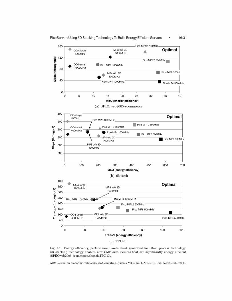
PicoServer: Using 3D Stacking Technology To Build Energy Efficient Servers • 16:31
Fig. 15. Energy efficiency, performance Pareto chart generated for 90nm process technology.
3D stacking technology enables new CMP architectures that are significantly energy efficient
(SPECweb2005-ecommerce,dbench,TPC-C).
ACM Journal on Emerging Technologies in Computing Systems, Vol. 4, No. 4, Article 16, Pub. date: October 2008.
16:32 • T. Kgil et al.
that enables a reduction in core clock frequency while providing high through-put. A sweetspot in system-level energy efficiency for our plotted datapointscan also be identified among the PicoServer architectures when comparing PicoMP4-500MHz, MP8-500MHz, and MP12-500MHz. These sweetspots in energyefficiency occur just before diminishing returns in throughput are reached asparallel processing is increased by adding more processors. The increase in par-allel processing raises many issues related to inefficient interrupt balancing,kernel process/thread scheduling, and resource allocation that result in dimin-ishing returns. Independent studies have shown the OS can be tuned to scalewith many cores [Bryant et al. 2004] and Shah et al. [2007] is an example ofsuch an implementation. However, we feel further investigation is necessaryand leave such work for future research.
6. CONCLUSIONS
In this article, we show the potential of 3D stacking technology to build energyefficient servers. For a wide set of server workloads, the resulting systems havesignificant energy efficiency in a compact form factor. A 12-way PicoServer run-ning at 500MHz can deliver 1Gbps of network bandwidth within a 3W powerbudget using a 90nm process technology. These power results are 2∼3× betterthan a multicore architecture without 3D stacking technology and an order ofmagnitude better than what can be achieved using a general purpose processor.The ability to tightly couple large amounts of memory to the cores through wideand low-latency interconnect pays dividends by reducing system complexity andcreates opportunities to implement system memory with nonuniform access la-tency. 3D technology enables core-to-DRAM interfaces that are high through-put while consuming low power. With the access latency of on-chip DRAM beingcomparable to the L2 cache, the L2 cache die area can be replaced with addi-tional cores, resulting in core clock frequency reduction while achieving higherthroughput. Compared to a conventional 8-way 1GHz chip multiprocessor witha 2MB L2 cache, an area-equivalent 12-way PicoServer running at 500MHzyields an improvement in energy efficiency of more than 2×.
ACKNOWLEDGMENTS
We thank the anonymous reviewers for providing feedback.
REFERENCES
3DRISC. 2004. FaStack 3D RISC super-8051 microcontroller. http://www.tachyonsemi.com/
OtherICs/datasheets/TSCR8051Lx_1_5Web.pdf.
ARM11MPcore. 2004. ARM 11 MPcore. http://www.arm.com/products/CPUs/
ARM11MPCoreMultiprocessor.html.
BANERJEE, K., SOURI, S. J., KAPUR, P., AND SARASWAT, K. C. 2001. 3-D ICs: A novel chip design for
improving deep-submicrometer interconnect performance and systems-on-chip integration. Proc.IEEE 89, 5 (May), 602–533.
BARFORD, P. AND CROVELLA, M. 1998. Generating representative Web workloads for network and
server performance evaluation. In Measurement and Modeling of Computer Systems. 151–160.
BINKERT, N. L., DRESLINSKI, R. G., HSU, L. R., LIM, K. T., SAIDI, A. G., AND REINHARDT, S. K. 2006. The
M5 simulator: Modeling networked systems. IEEE Micro 26, 4 (Jul.-Aug.), 52–60.
ACM Journal on Emerging Technologies in Computing Systems, Vol. 4, No. 4, Article 16, Pub. date: October 2008.

PicoServer: Using 3D Stacking Technology To Build Energy Efficient Servers • 16:33
BLACK, B., ANNAVARAM, M., BREKELBAUM, N., DEVALE, J., JIANG, L., LOH, G. H., MCCAULE, D.,
MORROW, P., NELSON, D. W., PANTUSO, D., REED, P., RUPLEY, J., SHANKAR, S., SHEN, J. P., AND WEBB,
C. 2006. Die stacking (3D) microarchitecture. In the International Symposium on Microar-chitecture.
BLACK, B., NELSON, D., WEBB, C., AND SAMRA, N. 2004. 3D processing technology and its impact
on iA32 microprocessors. In Proceedings of the International Conference on Computer Design,
316–318.
BRYANT, R., HAWKES, J., STEINER, J., BARNES, J., AND HIGDON, J. 2004. Scaling Linux to the extreme
from 64 to 512 processors. In the Linux Symposium.
CHIANG, T.-Y., SOURI, S. J., CHUI, C. O., AND SARASWAT, K. C. 2001. Thermal analysis of
heterogeneous 3-D ICs with various integration scenario. In IEDM Tech. Digest, 681–
684.
CLARK, L. T., HOFFMAN, E. J., MILLER, J., BIYANI, M., LIAO, Y., STRAZDUS, S., MORROW, M., VERLARDE,
K. E., AND YARCH, M. A. 2001. An embedded 32-b microprocessor core for low-power and high-
performance applications. IEEE J. Solid State Circ. 36, 11 (Nov.), 1599–1608.
CONGDUC, E. L. 2004. Packet classification in the NIC for improved SMP-based Internet servers.
In Proceedings of the International Conference on Networking.
DAVIS, W. R., WILSON, J., MICK, S., XU, J., HUA, H., MINEO, C., SULE, A. M., STEER, M., AND FRANZON, P. D.
2005. Demystifying 3D ICs: The pros and cons of going vertical. IEEE Des. Test Comput. 22, 6,
498–510.
FLYNN, M. J. AND HUNG, P. 2004. Computer architecture and technology: Some thoughts on the
road ahead. In Proceedings of the International Conference on Engineering of ReconfigurableSystems and Algorithms, 3–16.
GHOSH, M. AND LEE, H.-H. S. 2007. Smart refresh: An enhanced memory controller design for
reducing energy in conventional and 3D die-stacked DRAMs. In Proceedings of the InternationalSymposium on Microarchitecture.
GOPLEN, B. AND SAPATNEKAR, S. S. 2005. Thermal via placement in 3D ICs. In Proceedings of theInternational Symposium on Physical Design, 167–174.
GUPTA, S., HILBERT, M., HONG, S., AND PATTI, R. 2004. Techniques for producing 3D ICs with high-
density interconnect. www.tezzaron.com/about/papers/ieee_vmic_2004_finalsecure.pdf.
HO, R. AND HOROWITZ, M. 2001. The future of wires. Proc. IEEE 89, 4 (Apr.).
HUANG, W., STAN, M. R., SKADRON, K., SANKARANARAYANAN, K., GHOSH, S., AND VELUSAM, S. 2004. Com-
pact thermal modeling for temperature-aware design. In Proceedings of the Design AutomationConference.
ITRS 2005. ITRS roadmap. Tech. Rep.
KGIL, T. 2007. Architecting energy efficient servers. Ph.D. thesis, University of Michigan.
KGIL, T. AND MUDGE, T. 2006. FlashCache: A NAND flash memory file cache for low power Web
servers. In Proceedings of the International Conference on Compilers, Architecture and Synthesisfor Embedded Systems.
KGIL, T., ROBERTS, D., AND MUDGE, T. 2008. Improving NAND flash based disk caches. In Proceed-ings of the International Symposium on Computer Architecture.
KONGETIRA, P., AINGARAN, K., AND OLUKOTUN, K. 2005. Niagara: A 32-way multithreaded Sparc
processor. IEEE Micro 25, 2 (Mar.), 21–29.
KOYANAGI, M. 2005. Different approaches to 3D chips. http://asia.stanford.edu/events/
Spring05/slides/051205-Koyanagi.pdf.
KUNKEL, S. R., EICKEMEYER, R. J., LIPASTI, M. H., MULLINS, T. J., O’KRAFKA, B., ROSENBERG, H., VANDER-
WIEL, S. P., VITALE, P. L., AND WHITLEY, L. D. 2000. A performance methodology for commercial
servers. IBM J. Res. Develop. 44, 6.
LAUDON, J. 2005. Performance/Watt: The new server focus. SIGARCH Comput. Archit. News 33, 4,
5–13.
LEE, K., NAKAMURA, T., ONO, T., YAMADA, Y., MIZUKUSA, T., HASHIMOTO, H., PARK, K., KURINO, H.,
AND KOYANAGI, M. 2000. Three-Dimensional shared memory fabricated using wafer stacking
technology. In IEDM Tech. Digest, 165–168.
LIM, K., RANGANATHAN, P., CHANG, J., PATEL, C., MUDGE, T., AND REINHARDT, S. 2008. Understanding
and designing new server architectures for emerging warehouse-computing environments. In
Proceedings of the International Symposium on Computer Architecture.
ACM Journal on Emerging Technologies in Computing Systems, Vol. 4, No. 4, Article 16, Pub. date: October 2008.
16:34 • T. Kgil et al.
LOI, G. L., AGRAWAL, B., SRIVASTAVA, N., LIN, S.-C., SHERWOOD, T., AND BANERJEE, K. 2006. A
thermally-aware performance analysis of vertically integrated (3-D) processor-memory hierar-
chy. In Proceedings of the Design Automation Conference.
LS3 2007. (LS)3-Libre streaming, Libre software, Libre standards an open multimedia stream-
ing project. http://streaming.polito.it/.
LU, J. 2005. Wafer-Level 3D hyper-integration technology platform. www.rpi.edu/~luj/RPI_3D_
Research_0504.pdf.
MACGILLIVRAY, G. 2005. Process vs. density in DRAMs. http://www.eetasia.com/ARTICLES/
2005SEP/B/2005SEP01_STOR_TA.pdf.
MALTZ, D. A. AND BHAGWAT, P. 1998. TCP splicing for application layer proxy performance. Res.
Rep. RC 21139, IBM. March.
MATICK, R. E. AND SCHUSTER, S. E. 2005. Logic-Based eDRAM: Origins and rationale for use. IBMJ. Res. Develop. 49, 1 (Jan.).
MicronDRAM 2008. The Micron system-power calculator. http://www.micron.com/support/
part_info/powercalc.
MUDGE, T. 2001. Power: A first-class architectural design constraint. IEEE Comput. 34, 4 (Apr.).
NetRAM. 2005. Evolution of network memory. http://www.jedex.org/images/pdf/jack_
troung_samsung.pdf.
NSNIC 2001. National semiconductor DP83820 10 / 100 / 1000 Mb/s PCI ethernet network
interface controller.
OHSAWA, T., FUJITA, K., HATSUDA, K., HIGASHI, T., SHINO, T., MINAMI, Y., NAKAJIMA, H., MORIKADO, M.,
INOH, K., HAMAMOTO, T., WATANABE, S., FUJII, S., AND FURUYAMA, T. 2006. Design of a 128-Mb SOI
DRAM Using the Floating Body Cell (FBC). IEEE J. Solid State Circ. 41, 1 (Jan).
OSDL. 2006. OSDL dataBase test suite. http://www.osdl.net/lab_activities/kernel_
testing/osdl_database_test_suite/.
RAHMAN, A. AND REIF, R. 2000. System-Level performance evaluation of three-dimensional inte-
grated circuits. IEEE Trans. VLSI 8.
RICCI, F., CLARK, L. T., BEATTY, T., YU, W., BASHMAKOV, A., DEMMONS, S., FOX, E., MILLER, J., BIYANI,
M., AND HAIGH, J. 2005. A 1.5GHz 90nm embedded microprocessor core. In Proceedings of theSymposium on VLSI Circuits.
RLDRAM. 2008. RLDRAMA memory. http://www.micron.com/products/dram/rldram/.
SCHUTZ, J. AND WEBB, C. 2004. A scalable X86 CPU design for 90 nm process. In Proceedings ofthe International Solid-State Circuits Conference.
SHAH, M., BARREH, J., BROOKS, J., GOLLA, R., GROHOSKI, G., GURA, N., HETHERINGTON, R., JORDAN, P.,
LUTTRELL, M., OLSON, C., SAHA, B., SHEAHAN, D., SPRACKLEN, L., AND WYNN, A. 2007. UltraSPARC
T2: A highly-threaded, power-efficient, SPARC SOC. In Asian Solid-State Circuirts Conference.
SPECWeb. 1999. SPECweb99 benchmark. http://www.spec.org/osg/web99/.
SPECWeb. 2005. SPECweb2005 benchmark. http://www.spec.org/web2005/.
SUN FIRE T2000. 2008. Sun Fire T2000 server power calculator. http://www.sun.com/servers/
coolthreads/t2000/calc/index.jsp.
WENDELL, D., LIN, J., KAUSHIK, P., SESHADRI, S., WANG, A., SUNDARARAMAN, V., WANG, P., MCINTYRE,
H., KIM, S., HSU, W., PARK, H., LEVINSKY, G., LU, J., CHIRANIA, M., HEALD, R., AND LAZAR, P. 2004.
A 4MB on-chip l2 cache for a 90nm 1.6GHz 64b SPARC microprocessor. In Proceedings of theInternational Solid-State Circuits Conference.
XUE, L., LIU, C. C., KIM, H.-S., KIM, S., AND TIWARI, S. 2003. Three-Dimensional integration: Tech-
nology, use, and issues for mixed-signal applications. IEEE Trans. Electron Devices 50, 601–609.
Received November 2007; revised May 2008; accepted June 2008
ACM Journal on Emerging Technologies in Computing Systems, Vol. 4, No. 4, Article 16, Pub. date: October 2008.