PicoCOM Device Driver - F&S Elektronik Systeme GmbH€¦ · PicoCOM Device Driver Documentation...
55
PicoCOM Device Driver Documentation Version 1.9 (2013-03-28) PicoCOM Windows CE
Transcript of PicoCOM Device Driver - F&S Elektronik Systeme GmbH€¦ · PicoCOM Device Driver Documentation...

PicoCOMDevice Driver
Documentation
Version 1.9(2013-03-28)
PicoCOM
Windows CE


About This DocumentThis documentation describes the configuration and basic usage of all device drivers available for PicoCOM2, PicoCOM3, PicoCOM4 and PicoCOM5. Of course, we are targeting on keeping all modules of the PicoCOM family compatible, but because of different microprocessors, optimization fixes and customer suggestions, there might still remain some slight differences. Please keep this into account, when switching to a later PicoCOM board. Differences of each PicoCOM module are pointed out accordingly in this documentation.
The following abbreviations of terms are used in this documentation:
PC2 - PicoCOM2
PC3 - PicoCOM3
PC4 - PicoCOM4
PC5 - PicoCOM5
The latest version of this document can be found at:
http://www.picocom.de
Additional support information an software examples can be found in our discussion forum at:
http://forum.fs-net.de
© 2013
F&S Elektronik Systeme GmbHUntere Waldplätze 23
D-70569 StuttgartGermany
iii

iv
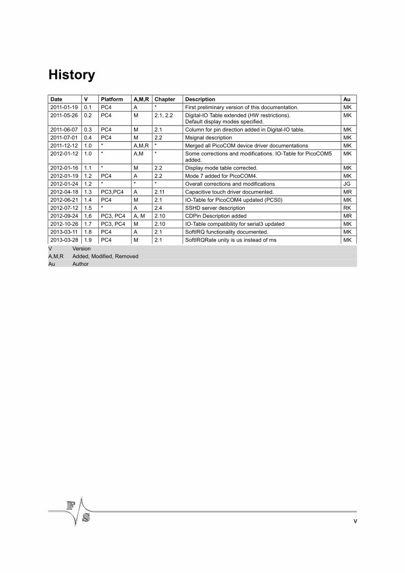
History
Date V Platform A,M,R Chapter Description Au
2011-01-19 0.1 PC4 A * First preliminary version of this documentation. MK
2011-05-26 0.2 PC4 M 2.1, 2.2 Digital-IO Table extended (HW restrictions).Default display modes specified.
MK
2011-06-07 0.3 PC4 M 2.1 Column for pin direction added in Digital-IO table. MK
2011-07-01 0.4 PC4 M 2.2 Msignal description MK
2011-12-12 1.0 * A,M,R * Merged all PicoCOM device driver documentations MK
2012-01-12 1.0 * A,M * Some corrections and modifications. IO-Table for PicoCOM5 added.
MK
2012-01-16 1.1 * M 2.2 Display mode table corrected. MK
2012-01-19 1.2 PC4 A 2.2 Mode 7 added for PicoCOM4. MK
2012-01-24 1.2 * * * Overall corrections and modifications JG
2012-04-18 1.3 PC3,PC4 A 2.11 Capacitive touch driver documented. MR
2012-06-21 1.4 PC4 M 2.1 IO-Table for PicoCOM4 updated (PCS0) MK
2012-07-12 1.5 * A 2.4 SSHD server description RK
2012-09-24 1,6 PC3, PC4 A, M 2.10 CDPin Description added MR
2012-10-26 1.7 PC3, PC4 M 2.10 IO-Table compatibility for serial3 updated MK
2013-03-11 1.8 PC4 A 2.1 SoftIRQ functionality documented. MK
2013-03-28 1.9 PC4 M 2.1 SoftIRQRate unity is us instead of ms MK
V Version
A,M,R Added, Modified, Removed
Au Author
v

Table of Contents1 Windows CE Stream Interface Driver 1
1.1 Common registry settings for Steam Interface Drivers.......................................21.2 Example of use..................................................................................................3
2 Device Driver 42.1 Driver for Digital I/O...........................................................................................42.1.1 IO-Pins...............................................................................................................62.1.2 Configuration example.....................................................................................112.1.3 Programming example.....................................................................................112.1.4 Troubleshooting...............................................................................................142.2 LCD-Display Driver...........................................................................................152.2.1 LCD power on sequences................................................................................212.3 Driver for Serial I/O (UART).............................................................................242.4 Audio Driver.....................................................................................................252.4.1 Volume controls...............................................................................................262.5 Ethernet Driver.................................................................................................272.6 I²C Device Driver..............................................................................................292.7 SPI Device Driver.............................................................................................292.8 CAN Device Driver...........................................................................................292.9 Analogue Input Driver......................................................................................302.9.1 Programming example.....................................................................................302.10 SD/MMC Card Driver.......................................................................................322.11 Touchpanel Driver............................................................................................342.11.1 Capacitive touch interface................................................................................36MXT224 Touch Driver....................................................................................................37EDT Touch Driver...........................................................................................................38
3 Modules and Utilities 393.1 NDCUCFG utility..............................................................................................393.2 Module NETUI..................................................................................................413.3 Core SSH support............................................................................................423.4 Extending the search path...............................................................................44
4 Appendix 45Listings..........................................................................................................................45List of Figures................................................................................................................45List of Tables..................................................................................................................45Important Notice............................................................................................................46
vi

vii


Windows CE Stream Interface Driver
1 Windows CE Stream Interface DriverMost Windows CE device drivers are implemented as Stream Interface Driver. Thus you can access these drivers via File System and the respective File API (CreateFile(), WriteFile(), ReadFile(), SetFilePointer(), DeviceIoControl()).
A Stream Interface Driver receives commands from the Device Manager and from applications by means of file system calls. The driver encapsulates all of the information that is necessary to translate those commands into appropriate actions on the devices it controls. All stream interface drivers, whether they manage built-in devices or installable devices, or whether they are loaded at boot time or loaded dynamically, have similar interactions with other system components. The following illustrations shows the interactions between system components for a generic stream interface driver, that manages a built-in device.
Figure 1: Windows CE Stream interface driver architecture.
All Stream Interface Drivers are loaded by the WindowsCE Device Manager during start-up. This mechanism can be controlled by registry settings under [HKLM\Drivers\Builtin]. These settings offer the possibility to define the load order and to disable several drivers independently.
1

Windows CE Stream Interface Driver
1.1 Common registry settings for Steam Interface Drivers
Table 1 shows a list of registry settings that are common for all drivers being loaded by the Device Manager.
Key Type Comment
Dll String Name of the DLL with the Driver
Order DWORD This value specifies the load order for the driver. If two drivers have the same load order value, the drivers load in the order they occur in the registry.A value of 0 authorises the device manager to load the driver in any order.Default: 0
Prefix String This required value specifies the driver’s device file name prefix. It is a three-character identifier, such as COM.
Index DWORD This required value specifies the device index, a value from 0 through 9.
Ioctl DWORD Call post-initialisation function.You should not modify this value.
Flags DWORD Load flags for the Device Manager.Possible values:0 = Default value if no flags are set.
1 = Tells the device manager to unload the driver after loading it and calling <XXX>_Init().
2 = Causes the driver to be loaded with a call to LoadLibrary() instead of LoadDriver()
4 = Allows you to have the registry settings loaded, but not the driver. You can use this to keep the driver from loading until you call ActivateDeviceEx() you can set this flag, but you must clear it before calling ActivateDeviceEx().
8 = Use this flag if you want to leave the prefix off of the driver functions.
Default: 0
FriendlyName
String Friendly name of the driver.
2

Windows CE Stream Interface Driver
Key Type Comment
IClass String Defines an interface class for the driver.Do not modify this value.
Table 1: Default stream driver regsitry settings.
1.2 Example of use
The device name to be used when accessing a driver, is composed by registry values Prefix and Index.
// Prefix = TST// Index = 2Handle hTst = CreateFile(_T("TST2:"), GENERIC_WRITE, 0, NULL,
OPEN_EXISTING, FILE_ATTRIBUTE_NORMAL, NULL);Listing 1: Accessing Device Drivers within an application.
For debugging issues or when desiring to use some interface pins for different purposes, it is often required to disable a device driver. To disable a driver from being loaded, registry value Flags must be set to 4:
[HKLM\Drivers\Builtin\<DriverName>]″Flags″=dword:4
Listing 2: Disabling a device driver via registry.
3

Device Driver
2 Device Driver
2.1 Driver for Digital I/O
PicoCOM features up to 49 programmable I/O lines. By default, no I/O line is configured by the Digital I/O driver (DIO). To control or access a pin with the DIO driver, it is required to adapt the configuration values in registry:
[HKLM\Drivers\BuiltIn\DIGITALIO]
Description of registry values:
Key Type Default value Comment
Port DWORD 0 This value defines the default port being used after opening the DIO driver.0,1,2,3,4 or 5
UseAsIO Hex 00,00,00, 00,00,00
1 = The corresponding pin is used as general purpose I/O. One bit for each I/O pin.
DataDir Hex 00,00,00, 00,00,00
Data Direction.
0 = The corresponding pin is an input.1 = The corresponding pin is an output.
One bit for each I/O pin.
DataInit Hex 00,00,00, 00,00,00
Default value of the output pin after driver initialization.
SoftIRQPriority256
DWORD 100 Priority of the polling thread used to handle software IRQ pins.
SoftIRQRate DWORD 10000 Polling rate to check pin state of software IRQ pions (in us).
IRQCFG0 Hex 00,00,00, 00,00,00
Interrupt configuration 0
0 = The corresponding pin is not configured to signal a raising edge.
1 = The corresponding pin is configured to signal a raising edge.
IRQCFG1 Hex 00,00,00, 00,00,00
Interrupt configuration 1
0 = The corresponding pin is not configured to signal a falling edge.
1 = The corresponding pin is configured to
4

Device Driver
signal a falling edge.
Table 2: Digital I/O registry settings.
Most I/O lines of the PicoCOM have multiple functions. Using a pin for the Digital I/O interface requires that all other corresponding functions are disabled. If I/O line 4 (pin 17) should be well configured and accessible by the DIO interface driver for example, the serial device driver for COM2 must be deactivated. Tables 4,5,6 and 7 will give you an overview of all I/O lines and their functions.
IRQCFG0 IRQCFG1 Function
0 0 Interrupt disabled
0 1 Falling edge enabled
1 0 Raising edge enabled
1 1 Raising and falling edge enabled
Table 3: Digital I/O interrupt configuration values.
Note:
On prior platforms I/O pins were configured in registry using 32-bit DWORD values (UseAsIOA, UseAsIOB, …). This method is still working on PicoCOM for compatibility purposes, but not explained in more detail at this point.
Note:
The SoftwareIRQ functionality enables possibility to use IRQ on all IO-Pins. This functionality is currently only available on PicoCOM4 (Kernel Version ≥ V1.12).
5

Device Driver
2.1.1 IO-Pins
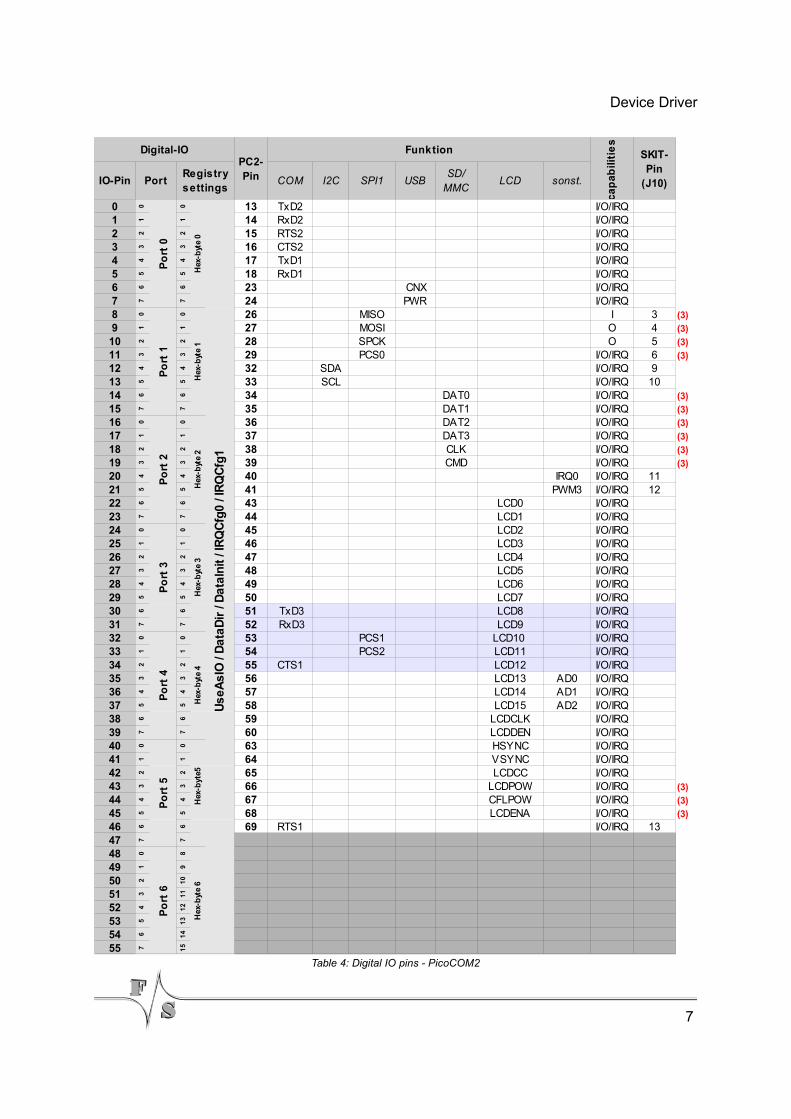
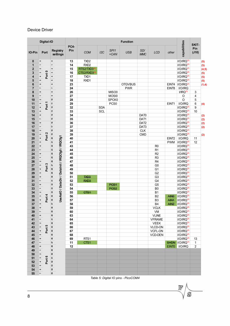
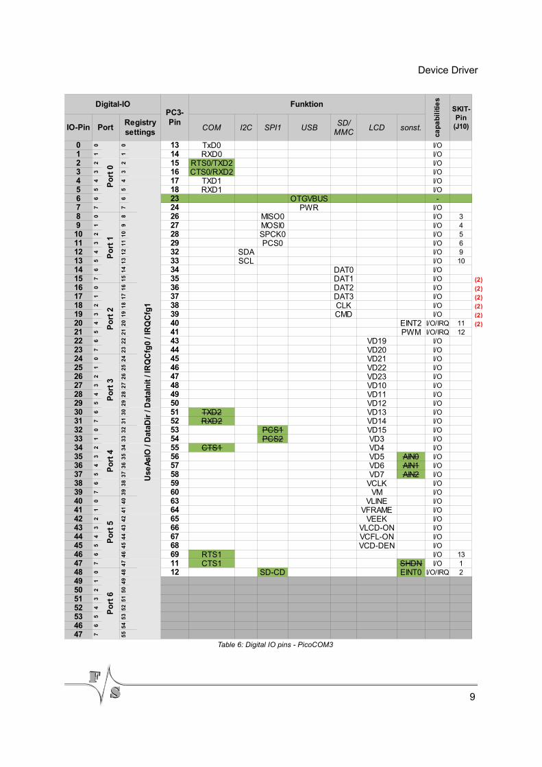
The tables available on the following sites show all pins, that can be configured and accessed by DIO driver interface. PicoCOM2 was the first board within the PicoCOM family, hence all later modules where designed to be as compatible to PicoCOM2 as possible. Pins that do not fully comply this compatibility, are marked with a green label to highlight the differences compared to PicoCOM2.
Additionally, please attend to marked hardware pin restrictions:
(1) Serial resistor (100k)
(2) Internal Pull-Up (10k)
(3) Pins may drive active signals during boot-up
(4) Since HW revision 1.2
(5) Software-IRQ only (refer to chapter 2.1)
Note:
Detailed information regarding particular IO-Pins can also be found in respective PicoCOM hardware documentation.
Note:
Please also note that not all IO-Pins feature the same capabilities. In contrary to PicoCOM2, on most other modules the interrupt capability is only available on a few pins. Please refer to column capabilities for details.
6
Device Driver
7
Table 4: Digital IO pins - PicoCOM2
Funktion
Port COM I2C SPI1 USB LCD sonst.
0 0
Po
rt 0
0 13 TxD2 I/O/IRQ1 1 1 14 RxD2 I/O/IRQ2 2 2 15 RTS2 I/O/IRQ3 3 3 16 CTS2 I/O/IRQ4 4 4 17 TxD1 I/O/IRQ5 5 5 18 RxD1 I/O/IRQ6 6 6 23 CNX I/O/IRQ7 7 7 24 PWR I/O/IRQ8 0
Po
rt 1
0 26 MISO I 3 (3)9 1 1 27 MOSI O 4 (3)10 2 2 28 SPCK O 5 (3)11 3 3 29 PCS0 I/O/IRQ 6 (3)12 4 4 32 SDA I/O/IRQ 913 5 5 33 SCL I/O/IRQ 1014 6 6 34 DAT0 I/O/IRQ (3)15 7 7 35 DAT1 I/O/IRQ (3)16 0
Po
rt 2
0 36 DAT2 I/O/IRQ (3)17 1 1 37 DAT3 I/O/IRQ (3)18 2 2 38 CLK I/O/IRQ (3)19 3 3 39 CMD I/O/IRQ (3)20 4 4 40 IRQ0 I/O/IRQ 1121 5 5 41 PWM3 I/O/IRQ 1222 6 6 43 LCD0 I/O/IRQ23 7 7 44 LCD1 I/O/IRQ24 0
Po
rt 3
0 45 LCD2 I/O/IRQ25 1 1 46 LCD3 I/O/IRQ26 2 2 47 LCD4 I/O/IRQ27 3 3 48 LCD5 I/O/IRQ28 4 4 49 LCD6 I/O/IRQ29 5 5 50 LCD7 I/O/IRQ30 6 6 51 TxD3 LCD8 I/O/IRQ31 7 7 52 RxD3 LCD9 I/O/IRQ32 0
Po
rt 4
0 53 PCS1 LCD10 I/O/IRQ33 1 1 54 PCS2 LCD11 I/O/IRQ34 2 2 55 CTS1 LCD12 I/O/IRQ35 3 3 56 LCD13 AD0 I/O/IRQ36 4 4 57 LCD14 AD1 I/O/IRQ37 5 5 58 LCD15 AD2 I/O/IRQ38 6 6 59 LCDCLK I/O/IRQ39 7 7 60 LCDDEN I/O/IRQ40 0
Po
rt 5
0
Hex
-byt
e5
63 HSYNC I/O/IRQ41 1 1 64 VSYNC I/O/IRQ42 2 2 65 LCDCC I/O/IRQ43 3 3 66 LCDPOW I/O/IRQ (3)44 4 4 67 CFLPOW I/O/IRQ (3)45 5 5 68 LCDENA I/O/IRQ (3)46 6 6 69 RTS1 I/O/IRQ 1347 7 7
48 0
Po
rt 6
8
49 1 9
50 2 10
51 3 11
52 4 12
53 5 13
54 6 14
55 7 15
Digital-IOPC2-Pin
cap
abili
tie
s
SKIT-Pin
(J10)IO-PinRegistry settings
SD/ MMC
Hex
-byt
e 0
Us
eA
sIO
/ D
ata
Dir
/ D
ata
Init
/ IR
QC
fg0
/ IR
QC
fg1
Hex
-byt
e 1
Hex
-byt
e 2
Hex
-byt
e 3
Hex
-byt
e 4
Hex
-byt
e 6
Device Driver
8
Table 5: Digital IO pins - PicoCOM4
Port COM I2C USB LCD
0 0
Po
rt 0
0 13 TXD2 (5)1 1 1 14 RXD2 (5)2 2 2 15 (4,5)3 3 3 16 (5)4 4 4 17 TXD1 (5)5 5 5 18 RXD1 (5)6 6 6 23 OTGVBUS EINT4 (1,4)7 7 7 24 PWR EINT8 I/O/IRQ8 0
Po
rt 1
8 26 MISO0 39 1 9 27 MOSI0 O 410 2 10 28 SPCK0 O 511 3 11 29 PCS0 EINT1 I/O/IRQ 6 (4)12 4 12 32 SDA 913 5 13 33 SCL 1014 6 14 34 DAT0 (2)15 7 15 35 DAT1 (2)16 0
Po
rt 2
16 36 DAT2 (2)17 1 17 37 DAT3 (2)18 2 18 38 CLK19 3 19 39 CMD (2)20 4 20 40 EINT2 I/O/IRQ 1121 5 21 41 PWM 1222 6 22 43 R023 7 23 44 R124 0
Po
rt 3
24 45 R225 1 25 46 R326 2 26 47 R427 3 27 48 G028 4 28 49 G129 5 29 50 G230 6 30 51 TXD3 G331 7 31 52 RXD3 G432 0
Po
rt 4
32 53 PCS1 G533 1 33 54 PCS2 B034 2 34 55 CTS1 B135 3 35 56 B2 AIN036 4 36 57 B3 AIN137 5 37 58 B4 AIN238 6 38 59 VCLK39 7 39 60 VM40 0
Po
rt 5
40 63 VLINE41 1 41 64 VFRAME42 2 42 65 VEEK43 3 43 66 VLCD-ON44 4 44 67 VCFL-ON45 5 45 68 VCD-DEN46 6 46 69 RTS1 1347 7 47 11 CTS1 SHDN 148 0
Po
rt 6
48 12 EINT0 I/O/IRQ 249 1 49
50 2 50
51 3 51
52 4 52
53 5 53
54 6 54
55 7 55
Digital-IO
PC4-Pin
Function
cap
ab
ilit
ies
SKIT-Pin (J10)IO-Pin
Registry settings
SPI1 +CAN
SD/ MMC
other
Use
AsI
O /
Da
taD
ir /
Da
taIn
it /
IR
QC
fg0
/ IR
QC
fg1
I/O/IRQ(5)
I/O/IRQ(5)
RTS2/TXD3(4) I/O/IRQ(5)
CTS2/RXD3(4) I/O/IRQ(5)
I/O/IRQ(5)
I/O/IRQ(5)
I/O/IRQ(4)
I/IRQ(5)
I/O/IRQ(5)
I/O/IRQ(5)
I/O/IRQ(5)
I/O/IRQ(5)
I/O/IRQ(5)
I/O/IRQ(5)
I/O/IRQ(5)
I/O/IRQ(5)
I/O/IRQ(5)
I/O/IRQ(5)
I/O/IRQ(5)
I/O/IRQ(5)
I/O/IRQ(5)
I/O/IRQ(5)
I/O/IRQ(5)
I/O/IRQ(5)
I/O/IRQ(5)
I/O/IRQ(5)
I/O/IRQ(5)
I/O/IRQ(5)
I/O/IRQ(5)
I/O/IRQ(5)
I/O/IRQ(5)
I/O/IRQ(5)
I/O/IRQ(5)
I/O/IRQ(5)
I/O/IRQ(5)
I/O/IRQ(5)
I/O/IRQ(5)
I/O/IRQ(5)
I/O/IRQ(5)
I/O/IRQ(5)
I/O/IRQ(5)
I/O/IRQ(5)
I/O/IRQ(5)
Device Driver
9
Table 6: Digital IO pins - PicoCOM3
Funktion
Port COM I2C SPI1 USB LCD sonst.
0 0
Po
rt 0
0 13 TxD0 I/O1 1 1 14 RXD0 I/O2 2 2 15 RTS0/TXD2 I/O3 3 3 16 CTS0/RXD2 I/O4 4 4 17 TXD1 I/O5 5 5 18 RXD1 I/O6 6 6 23 OTGVBUS -7 7 7 24 PWR I/O8 0
Po
rt 1
8 26 MISO0 I/O 39 1 9 27 MOSI0 I/O 410 2 1
0 28 SPCK0 I/O 511 3 1
1 29 PCS0 I/O 612 4 1
2 32 SDA I/O 913 5 1
3 33 SCL I/O 1014 6 1
4 34 DAT0 I/O15 7 1
5 35 DAT1 I/O (2)16 0
Po
rt 2
16 36 DAT2 I/O (2)
17 1 17 37 DAT3 I/O (2)
18 2 18 38 CLK I/O (2)
19 3 19 39 CMD I/O (2)
20 4 20 40 EINT2 I/O/IRQ 11 (2)
21 5 21 41 PWM I/O/IRQ 12
22 6 22 43 VD19 I/O
23 7 23 44 VD20 I/O
24 0
Po
rt 3
24 45 VD21 I/O
25 1 25 46 VD22 I/O
26 2 26 47 VD23 I/O
27 3 27 48 VD10 I/O
28 4 28 49 VD11 I/O
29 5 29 50 VD12 I/O
30 6 30 51 TXD2 VD13 I/O
31 7 31 52 RXD2 VD14 I/O
32 0
Po
rt 4
32 53 PCS1 VD15 I/O
33 1 33 54 PCS2 VD3 I/O
34 2 34 55 CTS1 VD4 I/O
35 3 35 56 VD5 AIN0 I/O
36 4 36 57 VD6 AIN1 I/O
37 5 37 58 VD7 AIN2 I/O
38 6 38 59 VCLK I/O
39 7 39 60 VM I/O
40 0
Po
rt 5
40 63 VLINE I/O
41 1 41 64 VFRAME I/O
42 2 42 65 VEEK I/O
43 3 43 66 VLCD-ON I/O
44 4 44 67 VCFL-ON I/O
45 5 45 68 VCD-DEN I/O
46 6 46 69 RTS1 I/O 13
47 7 47 11 CTS1 SHDN I/O 1
48 0
Po
rt 6
48 12 SD-CD EINT0 I/O/IRQ 2
49 1 49
50 2 50
51 3 51
52 4 52
53 5 53
46 6 54
47 7 55
Digital-IOPC3-Pin
cap
ab
ilit
ies
SKIT-Pin
(J10)IO-PinRegistry settings
SD/ MMC
Use
AsI
O /
Dat
aDir
/ D
ataI
nit
/ IR
QC
fg0
/ IR
QC
fg1

Device Driver
10
Table 7: Digital IO pins - PicoCOM5
Port COM I2C USB LCD
0 0
Po
rt 0
0 13 TXD2 I/O1 1 1 14 RXD2 I/O2 2 2 15 RTS2/TXD3 I/O3 3 3 16 CTS2/RXD3 I/O4 4 4 17 TXD1 I/O5 5 5 18 RXD1 I/O6 6 6 23 OTGVBUS - (1)7 7 7 24 PWR EINT4 I/O/IRQ8 0
Po
rt 1
8 26 MISO0 I/O 39 1 9 27 MOSI0 I/O 410 2 10 28 SPCK0 I/O 511 3 11 29 PCS0 I/O 612 4 12 32 SDA I/O 913 5 13 33 SCL I/O 1014 6 14 34 DAT0 I/O (2)15 7 15 35 DAT1 I/O (2)16 0
Po
rt 2
16 36 DAT2 I/O (2)17 1 17 37 DAT3 I/O (2)18 2 18 38 CLK I/O19 3 19 39 CMD I/O (2)20 4 20 40 EINT2 I/O/IRQ 1121 5 21 41 PWM/EINT3I/O/IRQ 1222 6 22 43 R1 I/O23 7 23 44 R2 I/O24 0
Po
rt 3
24 45 R3 I/O25 1 25 46 R4 I/O26 2 26 47 R5 I/O27 3 27 48 G0 I/O28 4 28 49 G1 I/O29 5 29 50 G2 I/O30 6 30 51 TXD3 G3 I/O31 7 31 52 RXD3 G4 I/O32 0
Po
rt 4
32 53 PCS1 G5 I/O33 1 33 54 PCS2 B1 I/O34 2 34 55 CTS1 B2 I/O35 3 35 56 B3 AIN0 I/O36 4 36 57 B4 AIN1 I/O37 5 37 58 B5 AIN2 I/O38 6 38 59 VCLK I/O39 7 39 60 VM I/O40 0
Po
rt 5
40 63 I/O41 1 41 64 I/O42 2 42 65 VEEK I/O43 3 43 66 VLCD-ON I/O44 4 44 67 VCFL-ON I/O45 5 45 68 VCD-DEN I/O46 6 46 69 RTS1 I/O 1347 7 47 11 CTS1 EINT1 I/O/IRQ 148 0
Po
rt 6
48 12 EINT0 I/O/IRQ 249 1 49
50 2 50
51 3 51
52 4 52
53 5 53
46 6 54
47 7 55
Digital-IOPC5-Pin
Function
cap
ab
ilit
ies
SKIT-Pin
(J10)IO-PinRegistry settings
SPI1 +CAN
SD/ MMC
other
Use
AsI
O /
Da
taD
ir /
Da
taIn
it /
IR
QC
fg0
/ IR
QC
fg1
B0/HSyncR0/VSync
Device Driver
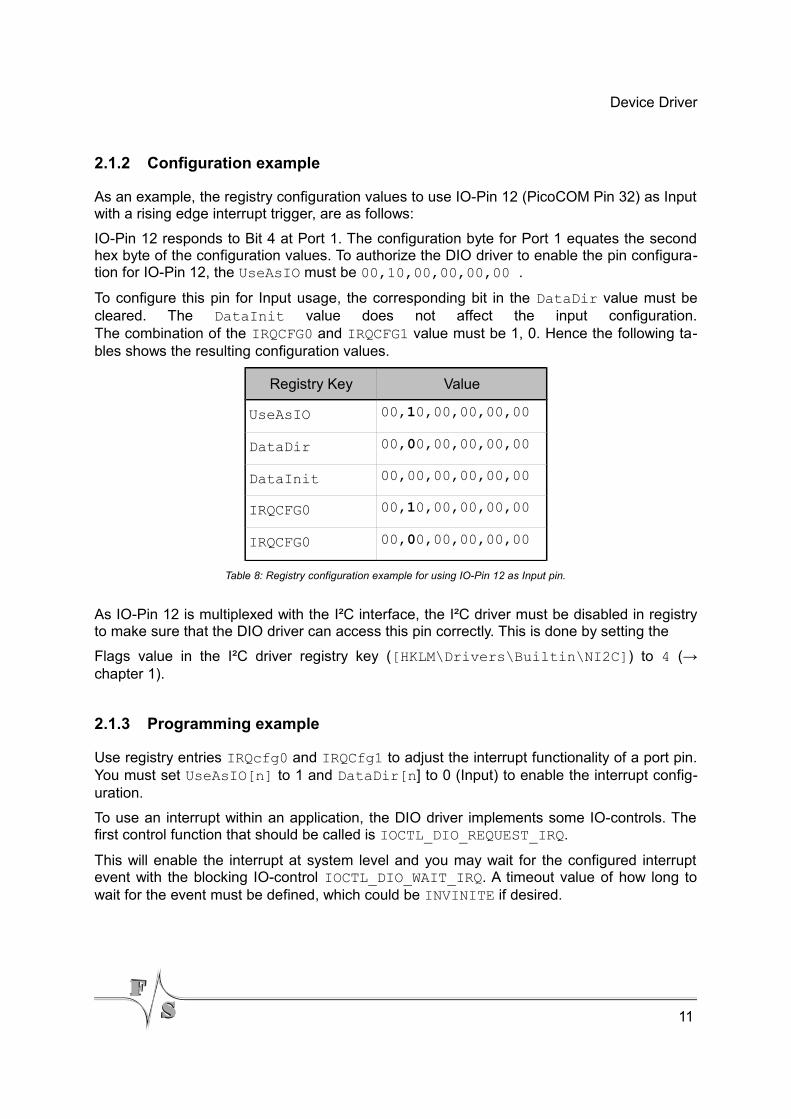
2.1.2 Configuration example
As an example, the registry configuration values to use IO-Pin 12 (PicoCOM Pin 32) as Input with a rising edge interrupt trigger, are as follows:
IO-Pin 12 responds to Bit 4 at Port 1. The configuration byte for Port 1 equates the second hex byte of the configuration values. To authorize the DIO driver to enable the pin configuration for IO-Pin 12, the UseAsIO must be 00,10,00,00,00,00 .
To configure this pin for Input usage, the corresponding bit in the DataDir value must be cleared. The DataInit value does not affect the input configuration.The combination of the IRQCFG0 and IRQCFG1 value must be 1, 0. Hence the following tables shows the resulting configuration values.
Registry Key Value
UseAsIO 00,10,00,00,00,00
DataDir 00,00,00,00,00,00
DataInit 00,00,00,00,00,00
IRQCFG0 00,10,00,00,00,00
IRQCFG0 00,00,00,00,00,00
Table 8: Registry configuration example for using IO-Pin 12 as Input pin.
As IO-Pin 12 is multiplexed with the I²C interface, the I²C driver must be disabled in registry to make sure that the DIO driver can access this pin correctly. This is done by setting the
Flags value in the I²C driver registry key ([HKLM\Drivers\Builtin\NI2C]) to 4 (→ chapter 1).
2.1.3 Programming example
Use registry entries IRQcfg0 and IRQCfg1 to adjust the interrupt functionality of a port pin. You must set UseAsIO[n] to 1 and DataDir[n] to 0 (Input) to enable the interrupt configuration.
To use an interrupt within an application, the DIO driver implements some IO-controls. The first control function that should be called is IOCTL_DIO_REQUEST_IRQ.
This will enable the interrupt at system level and you may wait for the configured interrupt event with the blocking IO-control IOCTL_DIO_WAIT_IRQ. A timeout value of how long to wait for the event must be defined, which could be INVINITE if desired.
11

Device Driver
As soon as the event is triggered or the timeout has expired, the DeviceIOControl() function will return and all actions, which are required to handle the interrupt, can be arranged.
For this reason, the interrupt will be disabled and has to be enabled again with the IOCTL_DIO_IRQ_DONE.
To unregister the interrupt, control code IOCTL_DIO_RELEASE_IRQ must be used. Please note that an interrupt has to be released before it can be reused and initialized again.
Example
#include <windows.h>#include <dio_sdk.h>
/* Main program */int _tmain(int argc, _TCHAR* argv[]){
/* -- 1.) Open one digital port -- */HANDLE hDIO;hDIO = CreateFile(_T("DIO1:"), GENERIC_WRITE, 0, NULL,
OPEN_EXISTING, FILE_ATTRIBUTE_NORMAL, NULL);
if (INVALID_HANDLE_VALUE == hDIO){
RETAILMSG(1, (L"CreateFile() failed (LE:%d)\r\n", GetLastEror()));
return(FALSE);}
/* -- 2.) Write data to the port -- */unsigned char data = 0xAA;DWORD dwBytesWrite = 1;WriteFile(hDIO, &data, dwBytesWrite, &dwBytesWrite, NULL);if (1 != dwBytesWrite){
/* TODO: Error handling */}
/* -- 3.) Change port -- */LONG lDistance = 1;if (!SetFilePointer(hDIO, lDistance, NULL, FILE_BEGIN)){
RETAILMSG(1, (L"SetFilePointer() failed (LE:%d)\r\n", GetLastError()));
}
/* -- 4.) Handle interrupt on port J5 pin 2 -- */BOOL bSuccess;DWORD dwIRQ, dwWaitState;WAITIRQ cIRQStat;dwIRQ = 12; /* PicoCOM4: IO-Pin12 - Pin32 - J10->Pin9 *//* Request interrupt */
12

Device Driver
if (!DeviceIoControl(hDIO, IOCTL_DIO_REQUEST_IRQ, &dwIRQ, sizeof(DWORD), NULL, 0, NULL, NULL)){
RETAILMSG(1,(L"Initializing interrupt failed (LE: %d)\n\r", GetLastError()));
return (FALSE);}while (TRUE){
/* Wait for interrupt (event)*/cIRQStat.dwTimeOut = 5000; /* maximum waittime: 5s */cIRQStat.dwIOPin = dwIRQ;bSuccess = DeviceIoControl(hDIO, IOCTL_DIO_WAIT_IRQ,
&cIRQStat, sizeof(cIRQStat), &dwWaitState,
sizeof(dwWaitState), NULL, NULL) ;
if (!bSuccess){
RETAILMSG(1, (L"IOCTL_DIO_WAIT_IRQ failed”));break;
}else if (WAIT_OBJECT_0 == dwWaitState){
RETAILMSG(1, (L"Interrpt occured!\r\n")) ;/* Acknowledge interrupt */bSuccess = DeviceIoControl(hDIO,
IOCTL_DIO_INTDONE_IRQ, &dwIRQ, sizeof(DWORD),
NULL, 0, NULL, NULL);}else{
RETAILMSG(1, (L"Timeout!\r\n"));}
}
/* Release IRQ */bSuccess = DeviceIoControl(hDIO, IOCTL_DIO_RELEASE_IRQ, &dwIRQ,
sizeof(DWORD), NULL, 0, NULL, NULL ) ;
if (!bSuccess){
RETAILMSG(1, (L"IOCTL_DIO_RELEASE_IRQ failed!\r\n", GetLastError()));
}
/* -- 5.) Close DIO driver -- */CloseHandle(hDIO);
} /* main() */Listing 3: Digital I/O programming example
13

Device Driver
2.1.4 Troubleshooting
1. Setting a non-working IO-Pin value:Please make sure that the UseAsIO and the DataDir registry values are set correctly. Meaning of each hex byte is:UseAsIO <Port0>, <Port1>, …, <Port5>, <Port6>Additionally, please make sure that the alternative function driver is disabled, as this leads to malfunction.
2. DIO driver reports different pin states when reading an input pin continuously.Please make sure that this pin has a certain level of using pull-up or pull-down resistors. Also verify that no external device is connected to this pin, that might influence its level.
14

Device Driver
2.2 LCD-Display Driver
PicoCOM features a very flexible and powerful interface for LCD displays. The driver is fully configurable via WindowsCE registry.
The registry key for the PicoCOM driver is:
[HKLM\Drivers\Display\LCD]
Use the following parameters to configure the driver:
Key Value Default value
Meaning
Mode DWORD PC2/4: 2PC3: 0
Number of the predefined configuration or new user configuration.
UseBootMem DWORD 0 Use memory provided by bootloader for frame buffer
Verbose DWORD 0 Enables additional output at serial debug port.
PWMDevice String “” Name of the PWM device being used for contrast control.Note: This device is always used if this key is defined in registry. The VEEK-Pin is no longer controlled by the display driver.
PWMFreq DWORD 0 Base-frequency for external PWM device.
Table 9: Basic display settings in registry.
With parameter Mode you have the possibility to use one of the fixed configurations stored in the kernel, or to define a new configuration in registry. Values between 0 and 99 are reserved for fixed configurations. For your own configuration you have to use values between 100 and 199.
The following configurations are predefined in the kernel:
Module Mode Display X´Y
PicoCOM2 0 Kyocera KCS3224 320x240
1 Sharp LM8V31 640x480
2 (default) Hitachi TX09 240x320
3 Sharp LQ057Q3DC02 320x240
4 Sharp LQ038Q5DR 320x240
15

Device Driver
Module Mode Display X´Y
5 Toshiba LTM04C280K 640x480
6 Sharp LQ104V1DG11 640x480
PicoCOM4
0 EDT ET035080 – 16Bpp, QVGA 320x240
1 EDT ET070080 – 16Bpp, WVGA 800x480
2 (default) Hitachi TX09 – 16Bpp, QVGA 240x320
3 EDT ET043080 – 16Bpp 480x272
4 NEC NL6448BC – 16Bpp, VGA 640x480
5 Sharp LQ104 – 16Bpp, VGA 640x480
6 AOU G104SN03 – 16Bpp, VGA (LVDS) 640x480
7 EDT ET057090DH – 16Bpp, VGA 640x480
PicoCOM3
0 (default) EDT ET070080 – 16Bpp, WVGA 800x480
1 EDT ET035080 – 16Bpp, QVGA 320x240
2 Hitachi TX09 – 16Bpp, QVGA 240x320
3 NEC NL6448BC – 16Bpp, VGA 640x480
4 Sharp LQ104 – 16Bpp, VGA 640x480
5 AOU G104SN03 – 16Bpp, VGA (LVDS) 640x480
6 AOU G104SN02 – 16Bpp, SVGA (LVDS) 800x600
7 Hitachi TX18D35 – 16Bpp, WVGA 800x480
Table 10: Predefined display modes.
16

Device Driver
For configurations with a mode higher than 99, you have to create a new sub-key with the Name Mode<n>. Within this sub-key you can use the following parameters to adjust the driver:
[HKLM\Drivers\Display\LCD\Mode<n>]
Key Type Meaning
Name String Name of the driver as a text string. Only for information purposes.
Type DWORD s. Table 12 - Display type settings.
Config DWORD s. Table 13 - Display config settings.
Columns DWORD Amount of visible pixels in X-direction.
PPL DWORD Amount of clocks in X-direction before the HSYNC signal.
This value is optional and normally the same number as Columns.
BLW DWORD1-256
Beginning-of-line-wait:Value (1-256) specifies the number of pixel clock periods to add to the beginning of a line transmission before the first set of pixels is sent to the display.
HSW DWORD1-64 (PC2)1-256(o.)
Horizontal-sync-pulse-width:Value (1-256) specifies the number of pixel clock periods to pulse the line clock at the end of each line.
Note:On PicoCOM2 the range of this value is restricted to 1-64 instead to 1-256.
ELW DWORD1-256
End-of-line-wait:Value (1-256) specifies the number of pixel clock periods to add to the end of a line transmission, before the line clock is asserted.
Rows DWORD Amount of visible pixels in Y-direction.
LPP DWORD Line per panel:This is an optional parameter and in most cases it is the same number as Rows.
BFW DWORD1-256
Beginning-of-frame wait:In TFT mode, value (1–256) specifies the number of line clock periods to add to the beginning of a frame, before the first set of pixels is sent to the display. The
17

Device Driver
Key Type Meaning
Line clock does toggle during the insertion of the extra line clock periods.
BFW must be cleared to zero (disabled) in passive mode.
VSW DWORD1-256
Vertical sync pulse width:In TFT mode, value (1–256) specifies the number of line clock periods to pulse the FRP pin at the end of each frame, after the end-of-frame wait (EFW) period elapses. Frame clock is used as VSYNC signal in active mode. The line clock does toggle during VSYNC.
Note:On PicoCOM2, the range of this value is restricted to 1-64 instead to 1-256.
In passive mode, the value (1–64) specifies the number of extra line clock periods to insert after the end-of-frame. The time for which FRP is asserted, is not affected by VSW in passive mode. The line clock does toggle during the insertion of the extra line clock periods.
EFW DWORD1-256
End-of-frame line clock wait count:In TFT mode, value (1–256) specifies the number of line clock periods to add to the end of each frame. The Line clock does toggle during the insertion of the extra line clock periods.
EFW must be cleared to zero (disabled) in passive mode.
Width DWORD Physical width of the display
Height DWORD Physical height of the display
Bpp DWORD Bits per Pixel.
The number of bits that represents one pixel in display memory.
ContrastEnable DWORD Switch on/off contrast voltage generation.
ContrastValue DWORD Initial value for contrast voltage.
LCDClk DWORD LCD pixel clock in Hz or MHz
Rotate DWORD Rotate Display (values: 0…4)
18
Device Driver
Key Type Meaning
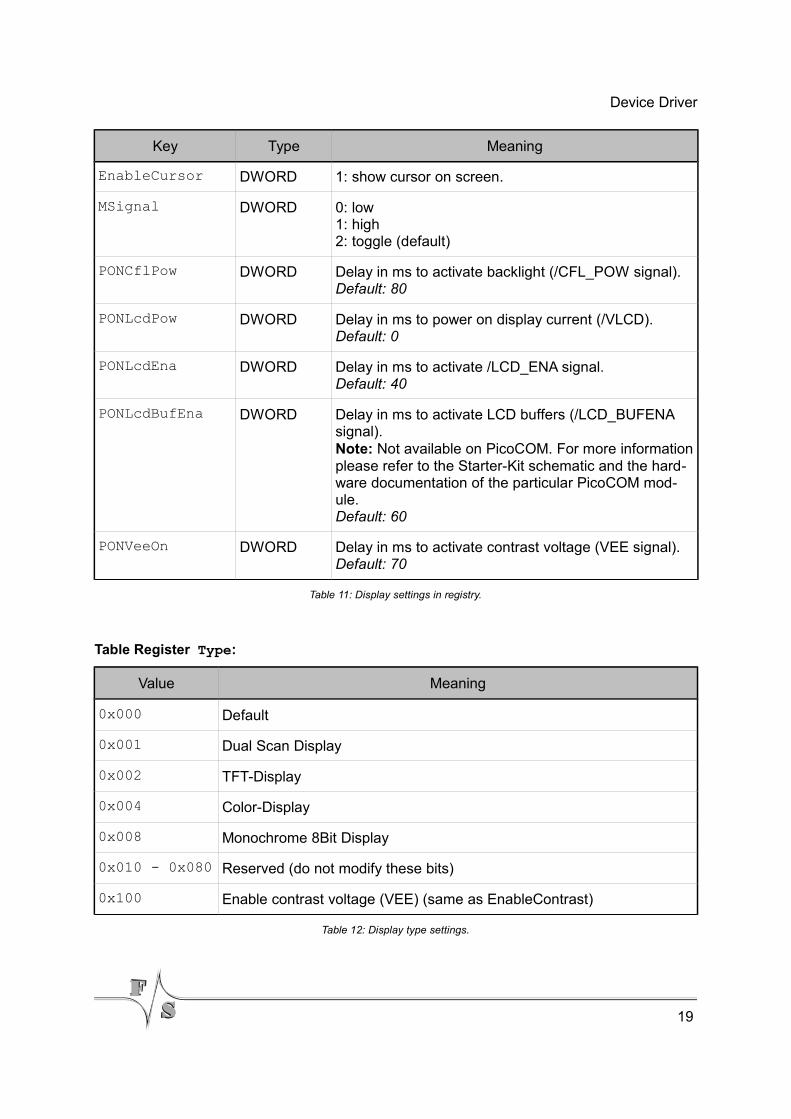
EnableCursor DWORD 1: show cursor on screen.
MSignal DWORD 0: low1: high2: toggle (default)
PONCflPow DWORD Delay in ms to activate backlight (/CFL_POW signal).Default: 80
PONLcdPow DWORD Delay in ms to power on display current (/VLCD).Default: 0
PONLcdEna DWORD Delay in ms to activate /LCD_ENA signal.Default: 40
PONLcdBufEna DWORD Delay in ms to activate LCD buffers (/LCD_BUFENA signal). Note: Not available on PicoCOM. For more information please refer to the Starter-Kit schematic and the hardware documentation of the particular PicoCOM module.Default: 60
PONVeeOn DWORD Delay in ms to activate contrast voltage (VEE signal).Default: 70
Table 11: Display settings in registry.
Table Register Type:
Value Meaning
0x000 Default
0x001 Dual Scan Display
0x002 TFT-Display
0x004 Color-Display
0x008 Monochrome 8Bit Display
0x010 - 0x080 Reserved (do not modify these bits)
0x100 Enable contrast voltage (VEE) (same as EnableContrast)
Table 12: Display type settings.
19
Device Driver
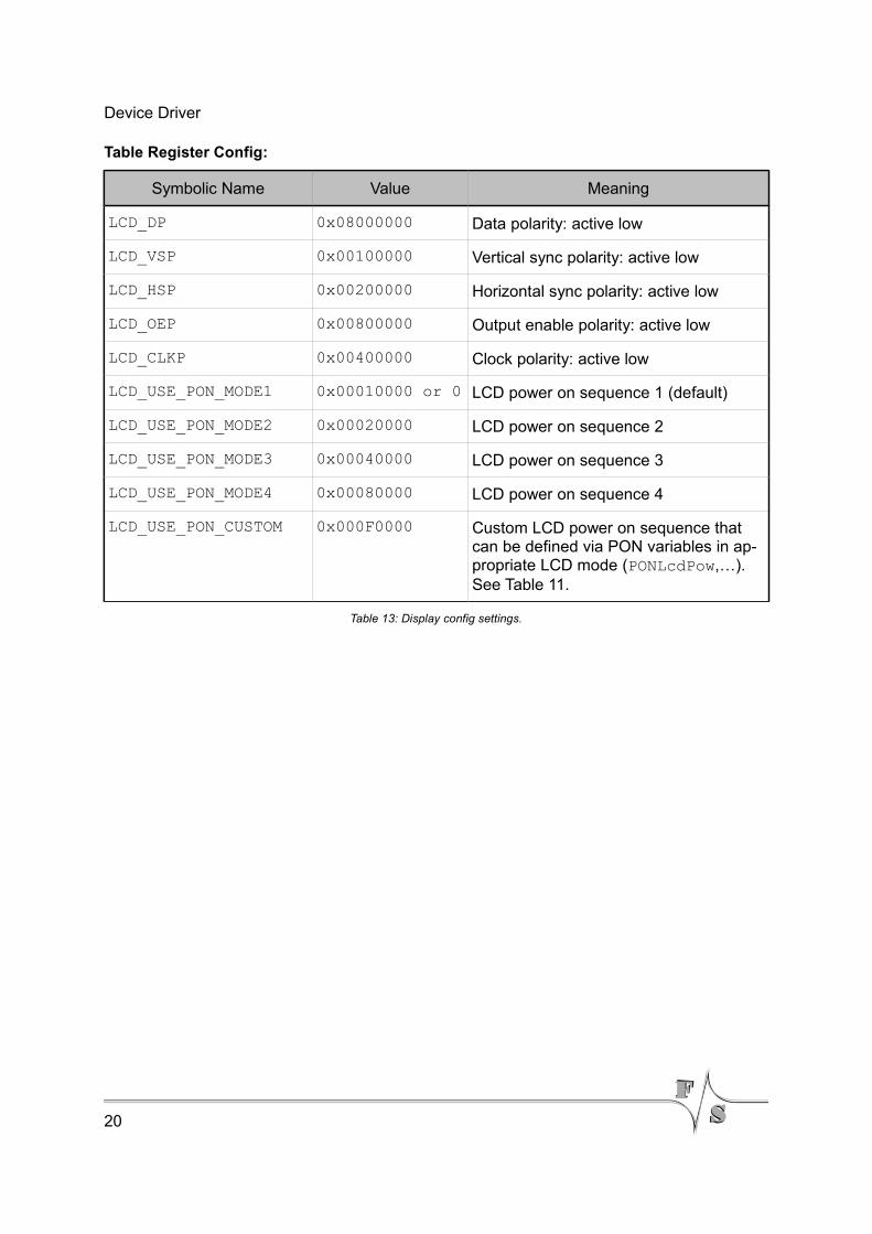
Table Register Config:
Symbolic Name Value Meaning
LCD_DP 0x08000000 Data polarity: active low
LCD_VSP 0x00100000 Vertical sync polarity: active low
LCD_HSP 0x00200000 Horizontal sync polarity: active low
LCD_OEP 0x00800000 Output enable polarity: active low
LCD_CLKP 0x00400000 Clock polarity: active low
LCD_USE_PON_MODE1 0x00010000 or 0 LCD power on sequence 1 (default)
LCD_USE_PON_MODE2 0x00020000 LCD power on sequence 2
LCD_USE_PON_MODE3 0x00040000 LCD power on sequence 3
LCD_USE_PON_MODE4 0x00080000 LCD power on sequence 4
LCD_USE_PON_CUSTOM 0x000F0000 Custom LCD power on sequence that can be defined via PON variables in appropriate LCD mode (PONLcdPow,…). See Table 11.
Table 13: Display config settings.
20

Device Driver
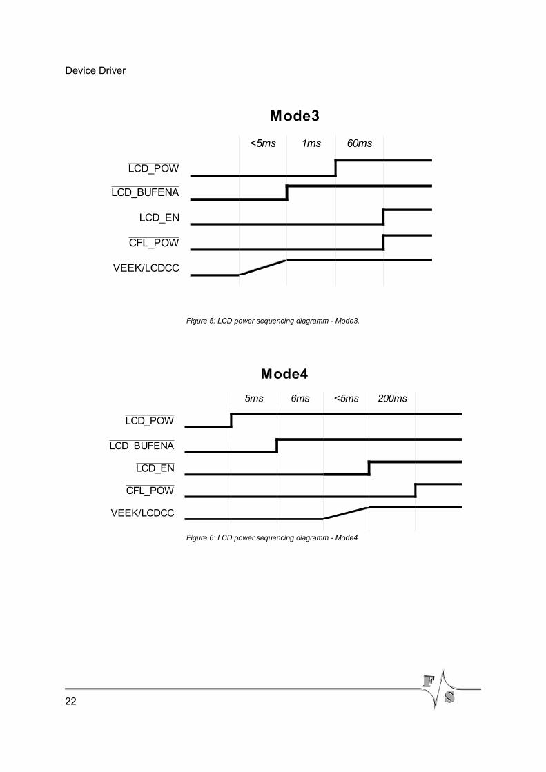
2.2.1 LCD power on sequences
21
Figure 4: LCD power sequencing diagramm - Mode1.
Mode1
<5ms 1ms 5ms
LCD_POW
LCD_BUFENA
LCD_EN
CFL_POW
VEEK/LCDCC
Figure 3: LCD power sequencing diagramm - Mode2.
Mode2
5ms <5ms 100ms
LCD_POW
LCD_BUFENA
LCD_EN
CFL_POW
VEEK/LCDCC
Figure 2: LCD power sequencing diagramm - Mode1.
Mode1
<5ms 1ms 5ms
LCD_POW
LCD_BUFENA
LCD_EN
CFL_POW
VEEK/LCDCC
Device Driver
22
Figure 5: LCD power sequencing diagramm - Mode3.
Mode3
<5ms 1ms 60ms
LCD_POW
LCD_BUFENA
LCD_EN
CFL_POW
VEEK/LCDCC
Figure 6: LCD power sequencing diagramm - Mode4.
Mode4
5ms 6ms <5ms 200ms
LCD_POW
LCD_BUFENA
LCD_EN
CFL_POW
VEEK/LCDCC
Device Driver
Note:
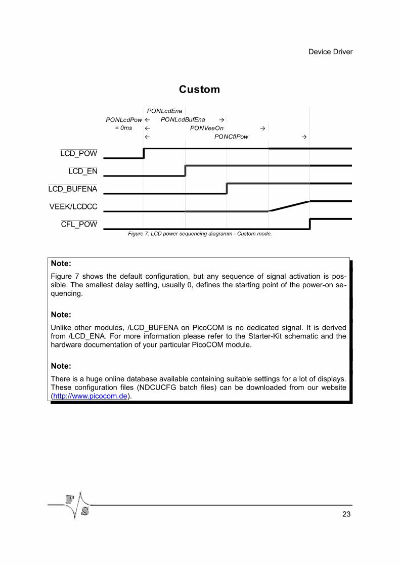
Figure 7 shows the default configuration, but any sequence of signal activation is possible. The smallest delay setting, usually 0, defines the starting point of the power-on sequencing.
Note:
Unlike other modules, /LCD_BUFENA on PicoCOM is no dedicated signal. It is derived from /LCD_ENA. For more information please refer to the Starter-Kit schematic and the hardware documentation of your particular PicoCOM module.
Note:
There is a huge online database available containing suitable settings for a lot of displays. These configuration files (NDCUCFG batch files) can be downloaded from our website (http://www.picocom.de).
23
Figure 7: LCD power sequencing diagramm - Custom mode.
LCD_POW
LCD_EN
LCD_BUFENA
VEEK/LCDCC
CFL_POW
Custom
PONLcdPow = 0ms
PONLcdEna
← PONLcdBufEna →← PONVeeOn →← PONCflPow →

Device Driver
2.3 Driver for Serial I/O (UART)
This driver is used to access serial interfaces COM1, COM2 and COM3.
The registry keys for the driver are:
[HKLM\Drivers\BuiltIn\SERIAL1][HKLM\Drivers\BuiltIn\SERIAL2][HKLM\Drivers\BuiltIn\SERIAL3]
Optional settings:
Key Type Default value Function
Priority256 DWORD 101 Priority for serial receive/transmit thread.
RS485 DWORD 0 Enable RS485 mode. This is only applicable for COM2.
Table 14: Serial I/O registry settings.
RS485 Mode
On PicoCOM you can toggle COM2 between RS232 and RS485 mode. To do this, you have to add the registry value RS485 and set it to 1. Additionally, you need to modify the fRtsControl member of DCB structure to enable RTS toggle control.
DCB cDCB;BOOL bSuccess;HANDLE hCOM2;
/* Open COM port*/hCOM2 = CreateFile(L"COM2", GENERIC_READ|GENERIC_WRITE, 0, NULL, OPEN_EXISTING, 0, 0);
/* Some basic strucutre initializations */cDCB.DCBlength = sizeof(DCB);//... e.g. set baudrate ...
/* Enable RTS toggle which is requored for RS485 mode */cDCB.fRtsControl = RTS_TOGGLE_CONTROL;
/* Apply DCB structure */bSuccess = SetComState(hCOM2, &cDCB);//...
Listing 4: Programming example how to set RTS toggle mode to enable RS485
24

Device Driver
Note:
Please note that RS485 requires a different external wiring.
2.4 Audio Driver
The Audio driver for PicoCOM can be configured under the following registry key:
[HKEY_LOCAL_MACHINE\Drivers\BuiltIn\Audio]
The mixer line settings are compatible across all Windows CE 6.0 based platforms.
Possible settings:
Key Value Type Default value Comment
Prefix String WAV This required value specifies the driver’s device file name prefix. It is a three-character identifier, such as COM.
DLL String wavedev.dll name of the driver file
Index DWORD:0-9
0 This value specifies the device index, a value from 0 through 9.
MasterOutMute DWORD:0/1
0 Mute all audio output channels.
MasterOutVol DWORD:0-0xFFFFFFFF
0xFFFFFFFF Main volume for all Output-channels.
OutputRenderMonoOnly
DWORD:0/1
0 If enabled, right channel output will be the same as left channel output.
EqPreset DWORD:0-2
0 Specifies the equalizer pre-set 0: Flat1: Min2: Max
TrebleBoost DWORD:0 – 0xF
0 Volume to control treble boost.
BassBoost DWORD0 – 0xFF
0 Bass boost volume
BypassMute DWORD0/1
1 Mute Line-In bypass.
25
Device Driver
Key Value Type Default value Comment
MasterInMute DWORD:0/1
1 Mute Line-In.
MasterInVol DWORD:0-0xFFFFFFFF
0 Main volume for all Input-channels.
LineInVol DWORD:0-0xFFFFFFFF
0 Volume for Line-In channel.
Table 15: Audio driver registry settings.
2.4.1 Volume controls
Please note that all volume controls separate into a left channel and a right channel value. More precisely, this means that the lower half bits are used for the right channel and the upper half bits are used for the left channel volume. In case of the Master output volume for example (MasterOutVol), the lower 16 bits (mask 0x0000FFFF) define the right channel volume and the higher 16 bits (mask: 0xFFFF0000) define the left channel volume.
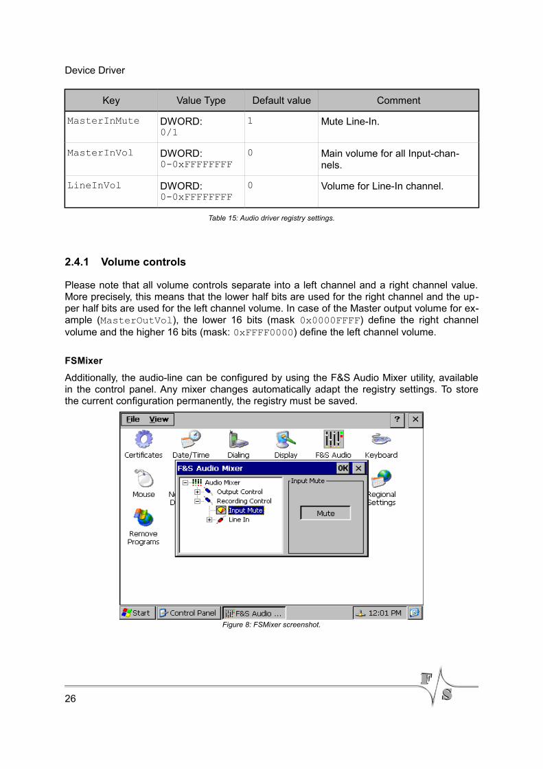
FSMixer
Additionally, the audio-line can be configured by using the F&S Audio Mixer utility, available in the control panel. Any mixer changes automatically adapt the registry settings. To store the current configuration permanently, the registry must be saved.
26
Figure 8: FSMixer screenshot.
Device Driver
2.5 Ethernet Driver
The Ethernet-Interface on PicoCOM features a small set of additional configurations:
[HKEY_LOCAL_MACHINE\Comm\ETHNETA1\Parms]
Implemented on: PC3, PC4
Key Value Type Default Value Comment
LinkMode DWORD:0-6
1 Enable/disable auto negotiation and select link speed .
1: AutoNegotiate 10/1002: AutoNegotiate 103: 100 Full Duplex4: 100 Half Duplex5: 10 Full Duplex6: 10 Half Duplex
PowerSavingLevel DWORD:0-2
0 Set power-saving level in case of unplugged cable0: No power saving1: Power-saving level 12: Power-saving level 2
Table 16: Ethernet driver registry settings.
Implemented on: PC2 only
Key Value Type Default Value Comment
LEDConfig DWORD0-8
8 Specifies the use of the LED0: Link OK1: RX or TX Activity2: TX Activity3: RX Activity4: Collision5: 100 Base-TX mode6: 10 Base-T mode7: Full Duplex8: Link OK / Blink on RX-TX Activity
27

Device Driver
Key Value Type Default Value Comment
TransmitGain DWORD0-3
1 Sets the transmit output amplitude0: 0dB1: 0.4dB2: 0.8 dB3: 1.2 dB
Speed DWORD0/10/100
1 Link speed in Mbit/s
FullDuplex DWORD0/1
1 Enable Full-Duplex mode
Table 17: Ethernet driver registry, settings for PicoCOM2 specifically.
Note:
To disable auto-negotiation, it is required to define the “Speed” and the “FullDuplex” value.
28

Device Driver
2.6 I²C Device Driver
The I²C interface driver is described in a separate documentation, that can be downloaded from http://www.picocom.de .
2.7 SPI Device Driver
The SPI interface driver is described in a separate documentation, that can be downloaded from http://www.picocom.de .
Note:
The SPI driver is not part of the default kernel image. To get more information of how to order this driver, please contact our sales department ([email protected])
2.8 CAN Device Driver
The CAN interface driver is described in a separated documentation, that can be downloaded from http://www.picocom.de .
29
Device Driver
2.9 Analogue Input Driver
Implemented on: PC2 only
PicoCOM2 features 3 analogue inputs. The channel to read from can either be selected with Channel registry value or dynamically by calling SetFilePointer() function.
The installation of the driver is done by setting some registry values under the following registry key:
[HKLM\Drivers\BuiltIn\ANALOGIN]
Required settings:
Key Value Type Default Value
Comment
Channel DWORD 0 Initial channel to be read from Channel can later be selected with SetFilePointer().
Timout DWORD 50 Timout in ms waits for a sample to be completed.
Table 18: Analog input registry settings.
The analogue interface driver implements the Stream Interface. After opening the channel by using CreateFile(), the ReadFile() function can be called to read one value from the currently selected channel. ReadFile() expects the value of the passed pointer to have the size of WORD (2bytes). To retrieve more than one sample, a buffer (array) of several WORDS can be passed to ReadFile().
2.9.1 Programming example
HANDLE hAIN;
/* open analog-in driver */hAIN = CreateFileW(L"AIN1:", GENERIC_READ|GENERIC_WRITE, 0, NULL, OPEN_EXISTING, 0, NULL);if (INVALID_HANDLE_VALUE != hAIN){ WORD wValue = 0; DWORD dwBytesRead; BOOL bNoError = TRUE; for(int i=0; i<3 && bNoError; i++)
30

Device Driver
{ /* select channel */ SetFilePointer(hAIN, i, NULL, FILE_BEGIN); /* sample analog value 10 times */ for(int n=10; n>0; n--) { if (ReadFile(hAIN, &wValue, 1, &dwBytesRead, NULL)) { RETAILMSG(1, (L"AIN value ch%d: %d\r\n", i, wValue)); } else { RETAILMSG(1, (L"Reading from analog in failed (LE: \ %d)\r\n", GetLastError())); } Sleep(2); } /* read loop */ } /* channel loop */ CloseHandle(hAIN);}else{ RETAILMSG(1, (L"Can not open 'AIN1:' (LE: %d)\r\n", GetLastError()));}
Listing 5: Analog Input programming example
31
Device Driver
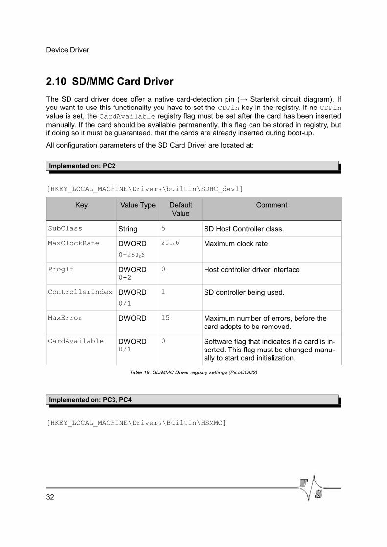
2.10 SD/MMC Card Driver
The SD card driver does offer a native card-detection pin (→ Starterkit circuit diagram). If you want to use this functionality you have to set the CDPin key in the registry. If no CDPin value is set, the CardAvailable registry flag must be set after the card has been inserted manually. If the card should be available permanently, this flag can be stored in registry, but if doing so it must be guaranteed, that the cards are already inserted during boot-up.
All configuration parameters of the SD Card Driver are located at:
Implemented on: PC2
[HKEY_LOCAL_MACHINE\Drivers\builtin\SDHC_dev1]
Key Value Type Default Value
Comment
SubClass String 5 SD Host Controller class.
MaxClockRate DWORD
0-250E6
250E6 Maximum clock rate
ProgIf DWORD0-2
0 Host controller driver interface
ControllerIndex DWORD
0/1
1 SD controller being used.
MaxError DWORD 15 Maximum number of errors, before the card adopts to be removed.
CardAvailable DWORD0/1
0 Software flag that indicates if a card is inserted. This flag must be changed manually to start card initialization.
Table 19: SD/MMC Driver registry settings (PicoCOM2)
Implemented on: PC3, PC4
[HKEY_LOCAL_MACHINE\Drivers\BuiltIn\HSMMC]
32

Device Driver
Key Value Type
Default Value
Comment
BaseClockFrequency DWORD 96000000 Base clock for internal SDHC controller.Do not change this value.
TimeoutClockFrequency
DWORD 96000000 Clock for SDHC timeout control.Do not change this value.
Irq DWORD 20 IRQ value.Do not change this value.
WriteProtect DWORD0/1
0 Software flag enable write-protection.
CardAvailable DWORD0/1
0 Software flag that indicates if a card is inserted. This flag must be changed manually to start card initialization.
CDPin DWORD -1 IRQ Pin if you want to use a SD Card Connection with a specific pin. If no value is set you have to set the CardAvailable Key manually.
Table 20: SD/MMC Driver registry settings (PicoCOM3, PicoCOM4)
33
Device Driver
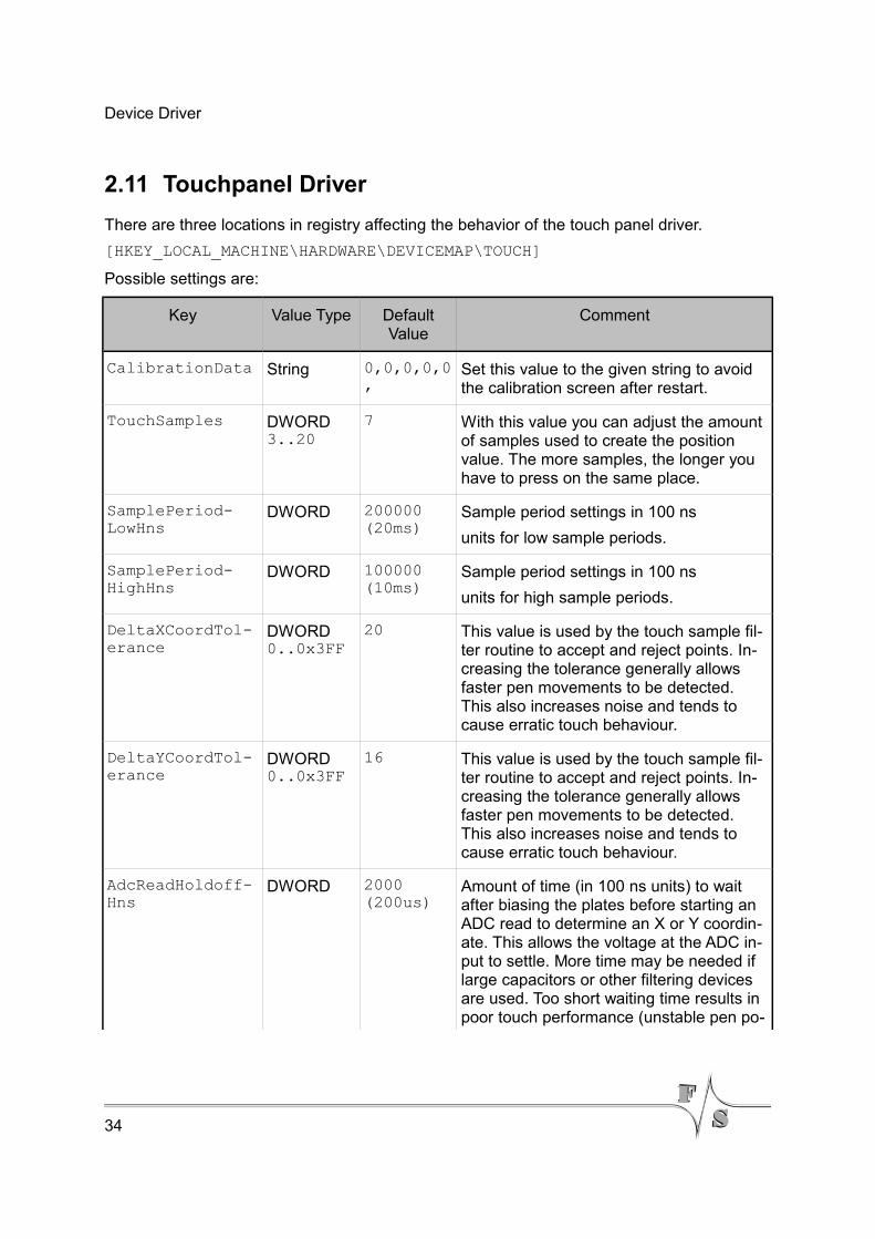
2.11 Touchpanel Driver
There are three locations in registry affecting the behavior of the touch panel driver.
[HKEY_LOCAL_MACHINE\HARDWARE\DEVICEMAP\TOUCH]
Possible settings are:
Key Value Type Default Value
Comment
CalibrationData String 0,0,0,0,0,
Set this value to the given string to avoid the calibration screen after restart.
TouchSamples DWORD3..20
7 With this value you can adjust the amount of samples used to create the position value. The more samples, the longer you have to press on the same place.
SamplePeriodLowHns
DWORD 200000 (20ms)
Sample period settings in 100 ns
units for low sample periods.
SamplePeriodHighHns
DWORD 100000(10ms)
Sample period settings in 100 ns
units for high sample periods.
DeltaXCoordTolerance
DWORD0..0x3FF
20 This value is used by the touch sample filter routine to accept and reject points. Increasing the tolerance generally allows faster pen movements to be detected. This also increases noise and tends to cause erratic touch behaviour.
DeltaYCoordTolerance
DWORD0..0x3FF
16 This value is used by the touch sample filter routine to accept and reject points. Increasing the tolerance generally allows faster pen movements to be detected. This also increases noise and tends to cause erratic touch behaviour.
AdcReadHoldoffHns
DWORD 2000 (200us)
Amount of time (in 100 ns units) to wait after biasing the plates before starting an ADC read to determine an X or Y coordinate. This allows the voltage at the ADC input to settle. More time may be needed if large capacitors or other filtering devices are used. Too short waiting time results in poor touch performance (unstable pen po
34

Device Driver
Key Value Type Default Value
Comment
sition). Too long waiting time causes poor system performance and may reduce the touch sampling frequency.
PenDownHoldoffHns
DWORD 50000(5ms)
Amount of time (in 100 ns units) to wait before reading the state of the plates, when determining whether the pen is up or down. Too short waiting makes it impossible for the driver to tell the true state of the plates, as the inputs will not have enough time to settle. This can cause the pen to get stuck in the down position. As with the AdcReadHoldOffDelay, this value may need to be increased if large capacitors or other hardware filtering is present. Too high value causes poor system performance and may reduce the touch sampling frequency.
MinMove DWORD1..0x3FF
5 Minimum move (A/D resolution) before MouseMove is signalled.
MaxMove DWORD1..0x3FF
50 Maximum move (A/D resolution) which is recognized and send to application layer.
AutoCalib DWORD0-10000
0 Time in ms before event “20” is signalled to application layer when touch is pressed. Can be used for automatic touch calibration.
AutoCalib=0 disables this function.
ADCConvFreq DWORD Default: 1000000
Debug DWORD: 0 Set to 4 to get list of registry settings at serial debug port.
Table 21: Touch driver registry settings
35

Device Driver
Calibration settings
[HKEY_LOCAL_MACHINE\SYSTEM\CALIBRUI]
Possible settings:
Key Value Type Default Value Comment
NoKeyboard DWORD 1 This parameter tells the touch panel calibration to not wait for a keystroke at the end of calibration.
Table 22: Touch driver calibration settings.
Touch driver priority
[HKEY_LOCAL_MACHINE\DRIVERS\BUILTIN\TOUCH]
Possible settings:
Key Value Type Default Value Comment
Priority256HighPriority256
DWORD 109 Set this value to adjust the priority of the touch panel driver.
Table 23: Touch driver priority settings.
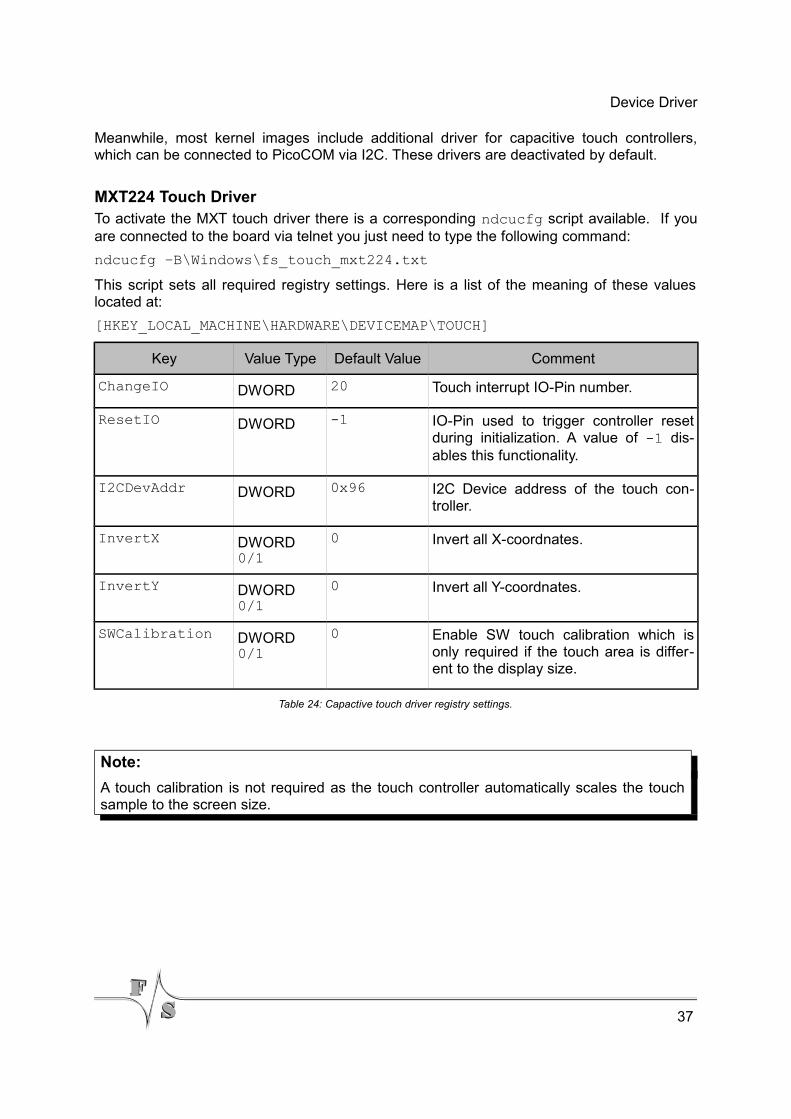
2.11.1 Capacitive touch interface
Implemented on: PC4, PC3
Capacitive touch interfaces are the latest touch screen technology, which uses measurable changes in capacitance of the screen's electrostatic field to determine the location of a touch. Unlike to resistive touch screens, this technology offers gesture and multi-touch capabilities which have become more important for application usability these days.
But as this touch technology by design requires customization for every hardware design it should be used on, it is not possible (yet) to use a touch controller module out of the shelf. There are lots of configuration settings that have to be parametrized (noise threshold,...). Thus we are working in close collaboration with our distributors. If you are interested in using capacitive touch screens in your application please contact our sales department ([email protected]) or contact your local distributor.
36
Device Driver
Meanwhile, most kernel images include additional driver for capacitive touch controllers, which can be connected to PicoCOM via I2C. These drivers are deactivated by default.
MXT224 Touch DriverTo activate the MXT touch driver there is a corresponding ndcucfg script available. If you are connected to the board via telnet you just need to type the following command:
ndcucfg –B\Windows\fs_touch_mxt224.txt
This script sets all required registry settings. Here is a list of the meaning of these values located at:
[HKEY_LOCAL_MACHINE\HARDWARE\DEVICEMAP\TOUCH]
Key Value Type Default Value Comment
ChangeIO DWORD 20 Touch interrupt IO-Pin number.
ResetIO DWORD -1 IO-Pin used to trigger controller reset during initialization. A value of -1 disables this functionality.
I2CDevAddr DWORD 0x96 I2C Device address of the touch controller.
InvertX DWORD0/1
0 Invert all X-coordnates.
InvertY DWORD0/1
0 Invert all Y-coordnates.
SWCalibration DWORD0/1
0 Enable SW touch calibration which is only required if the touch area is different to the display size.
Table 24: Capactive touch driver registry settings.
Note:
A touch calibration is not required as the touch controller automatically scales the touch sample to the screen size.
37

Device Driver
EDT Touch DriverIf you need to use the EDT touch driver there also is a corresponding ndcucfg script available. After you are connected to the board via telnet you just need to call the following command:
ndcucfg -B\Windows\fs_touch_edt.txt
This script sets all required registry settings. Here is a list of the meaning of these values located at:
[HKEY_LOCAL_MACHINE\HARDWARE\DEVICEMAP\TOUCH]
Key Value Type Default Value Comment
ChangeIO DWORD 20 Touch interrupt IO-Pin number.
ResetIO DWORD 21 IO-Pin used to trigger controller reset during initialization. A value of -1 disables this functionality.
I2CDevAddr DWORD 0x70 I2C Device address of the touch controller.
Table 25: Capactive touch driver registry settings.
After you activated this touch driver you should call the touch calibrate command, to use the touch panel correctly. Don't forget to save the registry settings with the reg save command.
38

Modules and Utilities
3 Modules and Utilities
3.1 NDCUCFG utility
This utility is always included in the WindowsCE image and enables access to the registry from the command line and to call some additional helper functions.
Ndcucfg.exe can be started via serial line, telnet or within a command window. By default, ndcucfg.exe is started from a Launch/Depend configuration in
[HKEY_LOCAL_MACHINE\Init]
and receives commands via serial line COM1. If you want to change the serial line, you can find settings of ndcucfg.exe under the following registry key:
[HKEY_LOCAL_MACHINE\System\NDCUCFG]
Possible settings:
Key Value Type Default Value Comment
Port String COM1: NDCUCFG will be started automatically during boot because of an entry in HKLM\Init key.
With this value you can specify which serial interface ndcucfg uses for communication.
BatchFile String The commands in the file specified here are executed during start of ndcucfg.
Table 26: ndcucfg registry settings.
List of commands (abstract):
display mode set <mode> Changes the display mode to the given number.
display mode get Retrieves the display mode.
display rotate get Retrieves the display rotation angle.
display rotate set <n> Changes the display rotation to the given angle. (possible values: 1…4)
reg open Opens the root key under HKLM
reg open <key> Opens the specified key under HKLM
reg enum Displays a list of all keys and values under the current location.
39

Modules and Utilities
reg opencu <key> Opens the specified key under HKCU
reg enum Displays a list of all keys and values under the current location
reg set value <name> dword <value>
Sets/creates the value with name <name> to the value <value>
reg set value <name> string <value>
reg set value <name> multi <value1>;<value2>
reg set value <name> hex <value>,<value>,<value>
reg create key <name> Creates the specified sub-key and opens it.
reg del value <name> Delete the specified value from registry.
reg del key <name> Delete the specified key from registry.
reg save Saves the registry in flash memory, so that modifications are available after reset.
fat format <volume> Formats the volume with name <volume>.
contrast + Increase contrast voltage of LCD (small steps)
contrast ++ Increase contrast voltage of LCD (large steps)
contrast - Decrease contrast voltage of LCD (small steps)
contrast -- Decrease contrast voltage of LCD (large steps)
contrast get Returns the current contrast voltage of LCD.
contrast set <n> Sets the contrast voltage of LCD. The value is the high time for the PWM circuit.
backlight on Switch on backlight of LCD.
backlight off Switch off backlight of LCD.
touch calibrate Shows the calibration screen for the touch panel.
sip on Shows the input panel window.
sip off Hides the input panel window.
reboot Reboots the device.
cert import cert <store> <file> Import certificate with filename <file> into certificate store <store>. Values for <store> MY, CA or ROOT.
cert import pkey <store> <file> Import private key from file into certificate store MY, CA or ROOT.
cert enum List all certificates from store MY, CA and ROOT.
cert delete <store> <store name> Delete certificate.
user create <name> <password> Creates new use with password.
user enum List all users
40
Modules and Utilities
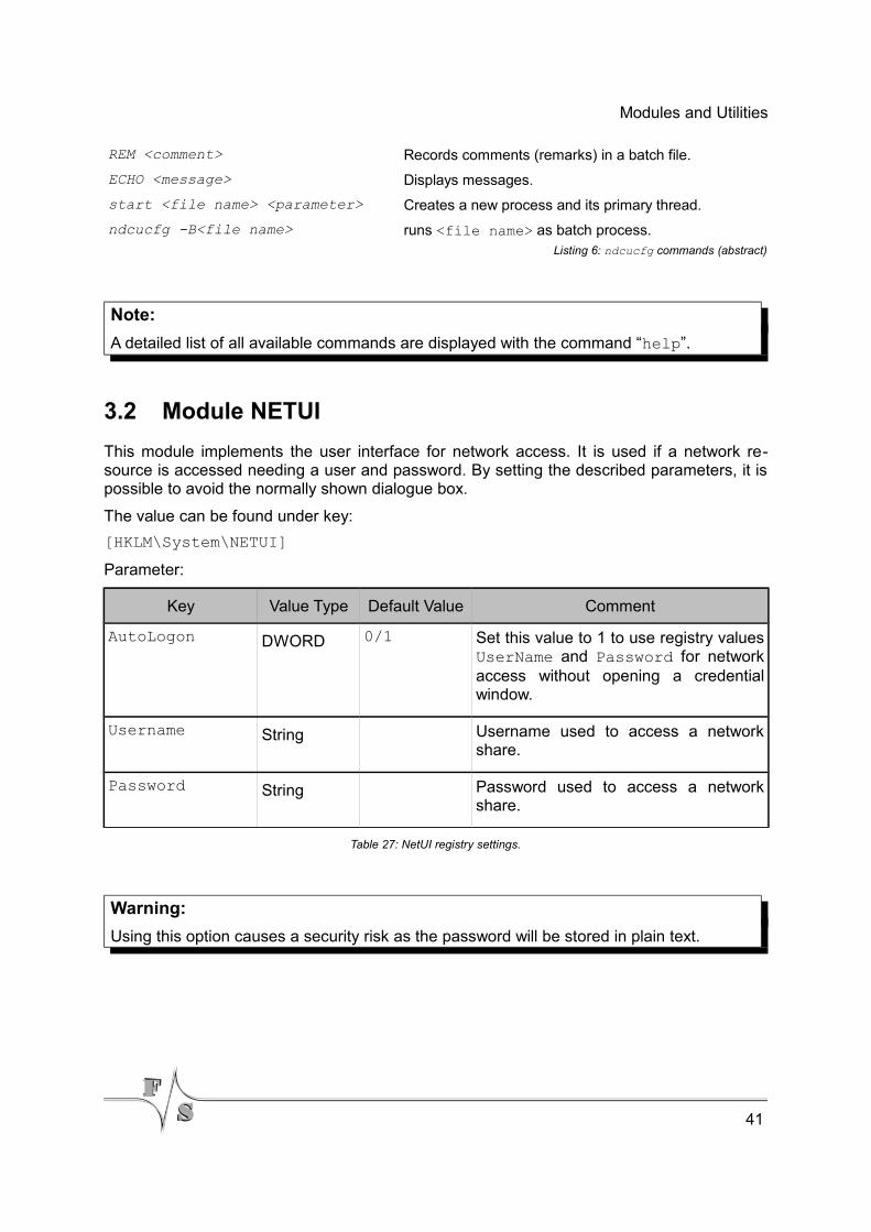
REM <comment> Records comments (remarks) in a batch file.
ECHO <message> Displays messages.
start <file name> <parameter> Creates a new process and its primary thread.
ndcucfg -B<file name> runs <file name> as batch process.Listing 6: ndcucfg commands (abstract)
Note:
A detailed list of all available commands are displayed with the command “help”.
3.2 Module NETUI
This module implements the user interface for network access. It is used if a network resource is accessed needing a user and password. By setting the described parameters, it is possible to avoid the normally shown dialogue box.
The value can be found under key:
[HKLM\System\NETUI]
Parameter:
Key Value Type Default Value Comment
AutoLogon DWORD 0/1 Set this value to 1 to use registry values UserName and Password for network access without opening a credential window.
Username String Username used to access a network share.
Password String Password used to access a network share.
Table 27: NetUI registry settings.
Warning:
Using this option causes a security risk as the password will be stored in plain text.
41

Modules and Utilities
3.3 Core SSH support
The SSH daemon is a Windows CE port based on the OpenSSH project. It makes encrypted communication between a client and our devices possible. To set up a connection to the device, you need a SSH client program. There are many programs like PuTTY or WinSCP available in the web. The original server program supports several authentication methods but this port includes only two of them. You can use the Password or the Private Key Authentication method. For a Password Authentication you have to creat a user with password on the device by using the NTLM protocol. Our standard utility NDCUFG (see chapter 3.1) have some command line functions based on the NTLM protocol that can be used. For the authentication methode Public Key you need a Public and a Private Key. The client use the Private Key to authententicate them against the server and the server need the Public Key to verify the Private Key. The most recommanded utility to generate the Keys is PuTTYgen. After generation the Public Key must be copied into the “authorized_keys2” file on the device and the Private Key is necessary on the client system. The server need additionally a Host Key named “ssh_host_dsa_key”. This key is used by the client and the server to encrypt and decrypt the communication data. You can also generate this key with PuTTYgen but our server generate a random Host Key automatically during first startup. It is possible to change some server settings in the “sshd_config” file. You can find the keys and the config file in the directory “FFSDISK\SSH\” on our devices. This port run as Windows service and can be started or stopped dynamically during runtime by using the services commands. There are also some registry parameters which can for example deactivate the SSH daemon completely.
The values can be found under key:
[HKLM\Services\SSHD]
Key Value Type Default Value Comment
Flags DWORD 0 or 16 Service is active. To deactivate it generally, set this value to 4.
Dll String Name of the library which is loaded by the Services.exe.
Order DWORD <10 Service load order.
Prefix String Präfix for the Services list.
Index DWORD 0 Service Index.
Keep DWORD 1 If Keep = 0, the DLL will be unloaded immediately after initialization.
ServiceContext DWORD 1 Initial value passed into the initialization routine.
42
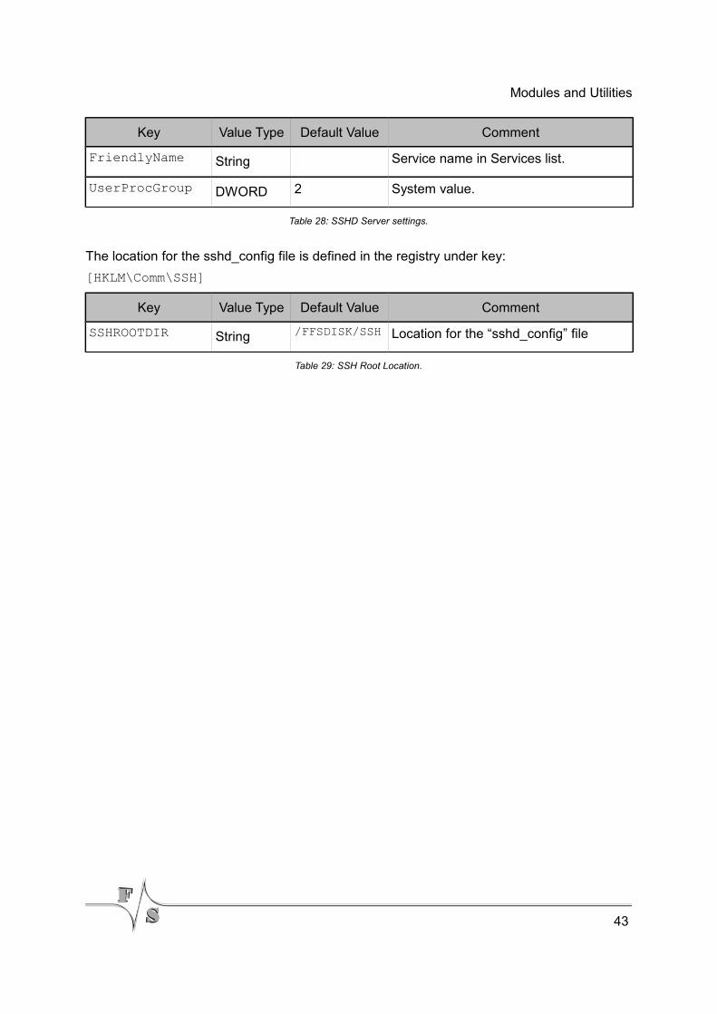
Modules and Utilities
Key Value Type Default Value Comment
FriendlyName String Service name in Services list.
UserProcGroup DWORD 2 System value.
Table 28: SSHD Server settings.
The location for the sshd_config file is defined in the registry under key:
[HKLM\Comm\SSH]
Key Value Type Default Value Comment
SSHROOTDIR String /FFSDISK/SSH Location for the “sshd_config” file
Table 29: SSH Root Location.
43

Modules and Utilities
3.4 Extending the search path
It is possible to extend the default path, which the kernel uses to locate executable files. The necessary entry can be found under registry key:
[HKEY_LOCAL_MACHINE\Loader]
Possible settings:
Key Value Type Default Value Comment
SystemPath Multi \\FFSDISK\\ To extend the path you must extend these values.
Table 30: Extending search path.
The SystemPath value has a maximum length of MAX_PATH characters, which includes the terminating NULL character. Any path specified by the OEM, is the last path to be when looking for a EXE. This registry value is only read during system boot.
44

Appendix
4 Appendix
Listings
Listing 1: Accessing Device Drivers within an application........................................................3
Listing 2: Disabling a device driver via registry........................................................................3
Listing 3: Digital I/O programming example..........................................................................13
Listing 4: Programming example how to set RTS toggle mode to enable RS485.................24
Listing 5: Analog Input programming example......................................................................31
Listing 6: ndcucfg commands (abstract)...............................................................................41
List of Figures
Figure 1: Windows CE Stream interface driver architecture....................................................1
Figure 2: LCD power sequencing diagramm - Mode1...........................................................21
Figure 3: LCD power sequencing diagramm - Mode2...........................................................21
Figure 4: LCD power sequencing diagramm - Mode1...........................................................21
Figure 5: LCD power sequencing diagramm - Mode3...........................................................22
Figure 6: LCD power sequencing diagramm - Mode4...........................................................22
Figure 7: LCD power sequencing diagramm - Custom mode................................................23
Figure 8: FSMixer screenshot...............................................................................................26
List of Tables
Table 1: Default stream driver regsitry settings.......................................................................3
Table 2: Digital I/O registry settings.........................................................................................5
Table 3: Digital I/O interrupt configuration values....................................................................5
Table 4: Digital IO pins - PicoCOM2........................................................................................7
Table 5: Digital IO pins - PicoCOM4........................................................................................8
Table 6: Digital IO pins - PicoCOM3........................................................................................9
Table 7: Digital IO pins - PicoCOM5......................................................................................10
45

Appendix
Table 8: Registry configuration example for using IO-Pin 12 as Input pin.............................11
Table 9: Basic display settings in registry..............................................................................15
Table 10: Predefined display modes.....................................................................................16
Table 11: Display settings in registry......................................................................................19
Table 12: Display type settings..............................................................................................19
Table 13: Display config settings...........................................................................................20
Table 14: Serial I/O registry settings.....................................................................................24
Table 15: Audio driver registry settings..................................................................................26
Table 16: Ethernet driver registry settings.............................................................................27
Table 17: Ethernet driver registry, settings for PicoCOM2 specifically...................................28
Table 18: Analog input registry settings.................................................................................30
Table 19: SD/MMC Driver registry settings (PicoCOM2).......................................................32
Table 20: SD/MMC Driver registry settings (PicoCOM3, PicoCOM4)....................................33
Table 21: Touch driver registry settings.................................................................................35
Table 22: Touch driver calibration settings.............................................................................36
Table 23: Touch driver priority settings..................................................................................36
Table 24: Capactive touch driver registry settings.................................................................37
Table 25: Capactive touch driver registry settings.................................................................38
Table 26: ndcucfg registry settings........................................................................................39
Table 27: NetUI registry settings...........................................................................................41
Table 28: SSHD Server settings............................................................................................43
Table 29: SSH Root Location................................................................................................43
Table 30: Extending search path...........................................................................................44
Important Notice
The information in this publication has been carefully checked and is believed to be entirely accurate at the time of publication. F&S Elektronik Systeme assumes no responsibility, however, for possible errors or omissions, or for any consequences resulting from the use of the information contained in this documentation.
F&S Elektronik Systeme reserves the right to make changes in its products or product specifications or product documentation with the intent to improve function or design at any time and without notice and is not required to update this documentation to reflect such changes.
F&S Elektronik Systeme makes no warranty or guarantee regarding the suitability of its products for any particular purpose, nor does F&S Elektronik Systeme assume any liability
46
Appendix
arising out of the documentation or use of any product and specifically disclaims any and all liability, including without limitation any consequential or incidental damages.
Products are not designed, intended, or authorised for use as components in systems intended for applications intended to support or sustain life, or for any other application in which the failure of the product from F&S Elektronik Systeme could create a situation where personal injury or death may occur. Should the buyer purchase or use a F&S Elektronik Systeme product for any such unintended or unauthorised application, the Buyer shall indemnify and hold F&S Elektronik Systeme and its officers, employees, subsidiaries, affiliates, and distributors harmless against all claims, costs, damages, expenses, and reasonable attorney fees arising out of, either directly or indirectly, any claim of personal injury or death that may be associated with such unintended or unauthorised use, even if such claim alleges that F&S Elektronik Systeme was negligent regarding the design or manufacture of said product.
47