PIC18F6393/6493/8393/8493 Data Sheetww1.microchip.com/downloads/en/DeviceDoc/39896a.pdf ·...
58
© 2007 Microchip Technology Inc. Preliminary DS39896A PIC18F6393/6493/8393/8493 Data Sheet 64/80-Pin High Performance, Flash Microcontrollers with LCD Driver, 12-Bit ADC and nanoWatt Technology
Transcript of PIC18F6393/6493/8393/8493 Data Sheetww1.microchip.com/downloads/en/DeviceDoc/39896a.pdf ·...
© 2007 Microchip Technology Inc. Preliminary DS39896A
PIC18F6393/6493/8393/8493Data Sheet
64/80-Pin High Performance,Flash Microcontrollers with LCD Driver,
12-Bit ADC and nanoWatt Technology

DS39896A-page ii Preliminary © 2007 Microchip Technology Inc.
Information contained in this publication regarding deviceapplications and the like is provided only for your convenienceand may be superseded by updates. It is your responsibility toensure that your application meets with your specifications.MICROCHIP MAKES NO REPRESENTATIONS ORWARRANTIES OF ANY KIND WHETHER EXPRESS ORIMPLIED, WRITTEN OR ORAL, STATUTORY OROTHERWISE, RELATED TO THE INFORMATION,INCLUDING BUT NOT LIMITED TO ITS CONDITION,QUALITY, PERFORMANCE, MERCHANTABILITY ORFITNESS FOR PURPOSE. Microchip disclaims all liabilityarising from this information and its use. Use of Microchipdevices in life support and/or safety applications is entirely atthe buyer�s risk, and the buyer agrees to defend, indemnify andhold harmless Microchip from any and all damages, claims,suits, or expenses resulting from such use. No licenses areconveyed, implicitly or otherwise, under any Microchipintellectual property rights.
Trademarks
The Microchip name and logo, the Microchip logo, Accuron, dsPIC, KEELOQ, KEELOQ logo, microID, MPLAB, PIC, PICmicro, PICSTART, PRO MATE, rfPIC and SmartShunt are registered trademarks of Microchip Technology Incorporated in the U.S.A. and other countries.
AmpLab, FilterLab, Linear Active Thermistor, Migratable Memory, MXDEV, MXLAB, SEEVAL, SmartSensor and The Embedded Control Solutions Company are registered trademarks of Microchip Technology Incorporated in the U.S.A.
Analog-for-the-Digital Age, Application Maestro, CodeGuard, dsPICDEM, dsPICDEM.net, dsPICworks, dsSPEAK, ECAN, ECONOMONITOR, FanSense, FlexROM, fuzzyLAB, In-Circuit Serial Programming, ICSP, ICEPIC, Mindi, MiWi, MPASM, MPLAB Certified logo, MPLIB, MPLINK, PICkit, PICDEM, PICDEM.net, PICLAB, PICtail, PowerCal, PowerInfo, PowerMate, PowerTool, REAL ICE, rfLAB, Select Mode, Smart Serial, SmartTel, Total Endurance, UNI/O, WiperLock and ZENA are trademarks of Microchip Technology Incorporated in the U.S.A. and other countries.
SQTP is a service mark of Microchip Technology Incorporated in the U.S.A.
All other trademarks mentioned herein are property of their respective companies.
© 2007, Microchip Technology Incorporated, Printed in the U.S.A., All Rights Reserved.
Printed on recycled paper.
Note the following details of the code protection feature on Microchip devices:� Microchip products meet the specification contained in their particular Microchip Data Sheet.
� Microchip believes that its family of products is one of the most secure families of its kind on the market today, when used in the intended manner and under normal conditions.
� There are dishonest and possibly illegal methods used to breach the code protection feature. All of these methods, to our knowledge, require using the Microchip products in a manner outside the operating specifications contained in Microchip�s Data Sheets. Most likely, the person doing so is engaged in theft of intellectual property.
� Microchip is willing to work with the customer who is concerned about the integrity of their code.
� Neither Microchip nor any other semiconductor manufacturer can guarantee the security of their code. Code protection does not mean that we are guaranteeing the product as �unbreakable.�
Code protection is constantly evolving. We at Microchip are committed to continuously improving the code protection features of ourproducts. Attempts to break Microchip�s code protection feature may be a violation of the Digital Millennium Copyright Act. If such actsallow unauthorized access to your software or other copyrighted work, you may have a right to sue for relief under that Act.
Microchip received ISO/TS-16949:2002 certification for its worldwide headquarters, design and wafer fabrication facilities in Chandler and Tempe, Arizona; Gresham, Oregon and design centers in California and India. The Company�s quality system processes and procedures are for its PIC® MCUs and dsPIC® DSCs, KEELOQ® code hopping devices, Serial EEPROMs, microperipherals, nonvolatile memory and analog products. In addition, Microchip�s quality system for the design and manufacture of development systems is ISO 9001:2000 certified.

© 2007 Microchip Technology Inc. Preliminary DS39896A-page 1
PIC18F6393/6493/8393/8493
LCD Driver Module Features:� Direct Driving of LCD Panel� Up to 192 Pixels: Software Selectable� Programmable LCD Timing module:
- Multiple LCD timing sources available- Up to four commons: Static, 1/2, 1/3 or
1/4 multiplex- Static, 1/2 or 1/3 bias configuration
� Can Drive LCD Panel while in Sleep mode for Low-Power Operation
Power-Managed Modes:� Run: CPU On, Peripherals On� Idle: CPU Off, Peripherals On� Sleep: CPU Off, Peripherals Off� Run mode Current Down to 14 μA Typical� Idle mode Currents Down to 5.8 μA Typical� Sleep mode Currents Down to 0.1 μA Typical� Timer1 Oscillator: 1.8 μA, 32 kHz, 2V� Watchdog Timer: 2.1 μA Typical� Two-Speed Oscillator Start-up
Flexible Oscillator Structure:� Four Crystal modes:
- LP: Up to 200 kHz- XT: Up to 4 MHz- HS: Up to 40 MHz- HSPLL: 4-10 MHz (16-40 MHz internal)
� 4x Phase Lock Loop (available for crystal and internal oscillators)
� Two External RC modes, Up to 4 MHz� Two External Clock modes, Up to 40 MHz� Internal Oscillator Block:
- Eight selectable frequencies, from 31 kHz to 8 MHz- Provides a complete range of clock speeds
from 31 kHz to 32 MHz when used with PLL- User-tunable to compensate for frequency drift
� Secondary Oscillator Using Timer1 at 32 kHz� Fail-Safe Clock Monitor:
- Allows for safe shutdown of device if primary or secondary clock fails
Peripheral Highlights:� 12-Bit, Up to 12-Channel Analog-to-Digital (A/D)
Converter module: - Auto-acquisition capability- Conversion available during Sleep
� High-Current Sink/Source 25 mA/25 mA� Four External Interrupts� Four Input Change Interrupts� Four 8-Bit/16-Bit Timer/Counter modules� Real-Time Clock (RTC) Software module:
- Configurable 24-hour clock, calendar, automatic 100-year or 12,800-year, day-of-week calculator
- Uses Timer1� Up to Two Capture/Compare/PWM (CCP) modules� Master Synchronous Serial Port (MSSP) module
Supporting Three-Wire SPI (all four modes) and I2C� Master and Slave modes
� Addressable USART module:- Supports RS-485 and RS-232
� Enhanced Addressable USART module:- Supports RS-485, RS-232 and LIN 1.2- Auto-wake-up on Start bit- Auto-Baud Detect
� Dual Analog Comparators with Input Multiplexing
Special Microcontroller Features:� C Compiler Optimized Architecture:
- Optional extended instruction set designed to optimize re-entrant code
� 1000 Erase/Write Cycle Flash Program Memory Typical
� Flash Retention: 100 Years Typical� Priority Levels for Interrupts� 8 x 8 Single-Cycle Hardware Multiplier� Extended Watchdog Timer (WDT):
- Programmable period from 4 ms to 132s- 2% stability over VDD and temperature
� In-Circuit Serial Programming� (ICSP�) via Two Pins� In-Circuit Debug (ICD) via Two Pins� Wide Operating Voltage Range: 2.0V to 5.5V
Note: This document is supplemented by the�PIC18F6390/6490/8390/8490 Data Sheet�(DS39629). See Section 1.0 �DeviceOverview�.
64/80-Pin High-Performance, Flash Microcontrollerswith LCD Driver, 12-Bit ADC and nanoWatt Technology

PIC18F6393/6493/8393/8493
DS39896A-page 2 Preliminary © 2007 Microchip Technology Inc.
Pin Diagrams
DeviceProgram Memory Data
MemoryI/O LCD
(pixel)
12-BitA/D
(channels)
CCP(PWM)
MSSP
EUSA
RT/
AU
SAR
T
Comparators Timers8/16-BitFlash
(bytes)# Single-WordInstructions
SRAM(bytes) SPI Master
I2C�
PIC18F6393 8K 4096 768 50 128 12 2 Y Y 1/1 2 1/3PIC18F6493 16K 8192 768 50 128 12 2 Y Y 1/1 2 1/3PIC18F8393 8K 4096 768 66 192 12 2 Y Y 1/1 2 1/3PIC18F8493 16K 8192 768 66 192 12 2 Y Y 1/1 2 1/3
64-Pin TQFP
Note 1: RE7 is the alternate pin for CCP2 multiplexing.
1234567891011121314
383736353433
50 49
17 18 19 20 21 22 23 24 25 26
LCD
BIA
S3
CO
M0
RE
4/C
OM
1R
E5/
CO
M2
RE
6/C
OM
3R
E7/
CC
P2(1
) /SE
G31
RD
0/S
EG0
VD
D
VS
S
RD
1/S
EG1
RD
2/S
EG2
RD
3/S
EG3
RD
4/S
EG4
RD
5/S
EG5
RD
6/S
EG6
RD
7/S
EG7
LCDBIAS2LCDBIAS1
RG0/SEG30RG1/TX2/CK2/SEG29RG2/RX2/DT2/SEG28
RG3/SEG27MCLR/VPP/RG5
RG4/SEG26VSS
VDD
RF7/SS/SEG25RF6/AN11/SEG24
RF5/AN10/CVREF/SEG23RF4/AN9/SEG22RF3/AN8/SEG21
RF2/AN7/C1OUT/SEG20
RB0/INT0RB1/INT1/SEG8RB2/INT2/SEG9RB3/INT3/SEG10RB4/KBI0/SEG11RB5/KBI1RB6/KBI2/PGCVSS
OSC2/CLKO/RA6OSC1/CLKI/RA7VDD
RB7/KBI3/PGD
RC4/SDI/SDARC3/SCK/SCLRC2/CCP1/SEG13
RF0
/AN
5/S
EG
18R
F1/A
N6/
C2O
UT/
SE
G19
AVD
D
AVS
S
RA
3/A
N3/
VRE
F+/S
EG
17R
A2/
AN2/
VRE
F-/S
EG
16R
A1/
AN
1R
A0/
AN
0V
SS
VD
D
RA
4/T0
CK
I/SEG
14R
A5/
AN4/
HLV
DIN
/SE
G15
RC
1/T1
OS
I/CC
P2(1
)
RC
0/T1
OS
O/T
13C
KI
RC
7/R
X1/
DT1
RC
6/TX
1/C
K1
RC5/SDO/SEG12
1516
31
4039
27 28 29 30 32
4847464544434241
54 53 52 5158 57 56 5560 5964 63 62 61
PIC18F6393PIC18F6493

© 2007 Microchip Technology Inc. Preliminary DS39896A-page 3
PIC18F6393/6493/8393/8493Pin Diagrams (Continued)
80-Pin TQFP
Note 1: RE7 is the alternate pin for CCP2 multiplexing.
345678910111213141516
4847464544434241
4039
64 63 62 61
21 22 23 24 25 26 27 28 29 30 31 32
LCD
BIA
S3
CO
M0
RE4
/CO
M1
RE5
/CO
M2
RE6
/CO
M3
RE7
/CC
P2(1
) /SE
G31
RD
0/S
EG
0V D
D
VSS
RD
1/S
EG
1R
D2/
SE
G2
RD
3/S
EG
3R
D4/
SE
G4
RD
5/S
EG
5R
D6/
SE
G6
RD
7/S
EG
7
LCDBIAS2LCDBIAS1
RG0/SEG30RG1/TX2/CK2/SEG29RG2/RX2/DT2/SEG28
RG3/SEG27MCLR/VPP/RG5
RG4/SEG26VSS
VDD
RF7/SS/SEG25
RB0/INT0RB1/INT1/SEG8RB2/INT2/SEG9RB3/INT3/SEG10RB4/KBI0/SEG11RB5/KBI1RB6/KBI2/PGCVSS
OSC2/CLKO/RA6OSC1/CLKI/RA7VDD
RB7/KBI3/PGD
RC4/SDI/SDARC3/SCK/SCLRC2/CCP1/SEG13
RF0
/AN
5/S
EG18
RF1
/AN
6/C
2OU
T/S
EG19
AVD
D
AVS
S
RA
3/A
N3/
VRE
F+/S
EG
17R
A2/A
N2/
VRE
F-/S
EG
16R
A1/
AN1
RA
0/AN
0V
SS
VD
D
RA
4/T0
CK
I/SE
G14
RA5
/AN
4/H
LVD
IN/S
EG
15
RC
1/T1
OS
I/CC
P2(1
)
RC
0/T1
OS
O/T
13C
KI
RC
7/R
X1/
DT1
RC
6/TX
1/C
K1
RC5/SDO/SEG12R
J0/S
EG
32R
J1/S
EG
33
RH
1/S
EG
46R
H0/
SEG
47
12
RH2/SEG45RH3/SEG44
1718
RH7/SEG43RH6/SEG42
RH
5/SE
G41
RH
4/SE
G40
RJ5
/SEG
38R
J4/S
EG39
37
RJ7/SEG36RJ6/SEG37
5049
RJ2/SEG34RJ3/SEG35
1920
33 34 35 36 38
5857565554535251
6059
68 67 66 6572 71 70 6974 7378 77 76 757980
RF5/AN10/CVREF/SEG23RF4/AN9/SEG22RF3/AN8/SEG21
RF2/AN7/C1OUT/SEG20
RF6/AN11/SEG24
PIC18F8393PIC18F8493
PIC18F6393/6493/8393/8493
DS39896A-page 4 Preliminary © 2007 Microchip Technology Inc.
Table of Contents1.0 Device Overview .......................................................................................................................................................................... 72.0 12-Bit Analog-to-Digital Converter (A/D) Module ....................................................................................................................... 293.0 Special Features of the CPU...................................................................................................................................................... 394.0 Electrical Characteristics ........................................................................................................................................................... 415.0 Packaging Information................................................................................................................................................................ 45Appendix A: Revision History............................................................................................................................................................... 47Appendix B: Device Differences........................................................................................................................................................... 47Appendix C: Conversion Considerations ............................................................................................................................................. 48Appendix D: Migration from Baseline to Enhanced Devices................................................................................................................ 48Appendix E: migration from Mid-Range to Enhanced Devices ............................................................................................................ 49Appendix F: Migration from High-End to Enhanced Devices ............................................................................................................... 49Index .................................................................................................................................................................................................... 51The Microchip Web Site ....................................................................................................................................................................... 53Customer Change Notification Service ................................................................................................................................................ 53Customer Support ................................................................................................................................................................................ 53Reader Response ................................................................................................................................................................................ 54Product Identification System............................................................................................................................................................... 55

© 2007 Microchip Technology Inc. Preliminary DS39896A-page 5
PIC18F6393/6493/8393/8493
TO OUR VALUED CUSTOMERSIt is our intention to provide our valued customers with the best documentation possible to ensure successful use of your Microchipproducts. To this end, we will continue to improve our publications to better suit your needs. Our publications will be refined andenhanced as new volumes and updates are introduced. If you have any questions or comments regarding this publication, please contact the Marketing Communications Department viaE-mail at [email protected] or fax the Reader Response Form in the back of this data sheet to (480) 792-4150. Wewelcome your feedback.
Most Current Data SheetTo obtain the most up-to-date version of this data sheet, please register at our Worldwide Web site at:
http://www.microchip.comYou can determine the version of a data sheet by examining its literature number found on the bottom outside corner of any page.The last character of the literature number is the version number, (e.g., DS30000A is version A of document DS30000).
ErrataAn errata sheet, describing minor operational differences from the data sheet and recommended workarounds, may exist for currentdevices. As device/documentation issues become known to us, we will publish an errata sheet. The errata will specify the revisionof silicon and revision of document to which it applies.To determine if an errata sheet exists for a particular device, please check with one of the following:� Microchip�s Worldwide Web site; http://www.microchip.com� Your local Microchip sales office (see last page)When contacting a sales office, please specify which device, revision of silicon and data sheet (include literature number) you areusing.
Customer Notification SystemRegister on our web site at www.microchip.com to receive the most current information on all of our products.

PIC18F6393/6493/8393/8493
DS39896A-page 6 Preliminary © 2007 Microchip Technology Inc.
NOTES:

© 2007 Microchip Technology Inc. Preliminary DS39896A-page 7
PIC18F6393/6493/8393/8493
1.0 DEVICE OVERVIEWThis document contains device-specific information forthe following devices:
This family offers the advantages of all PIC18microcontrollers � namely, high computationalperformance at an economical price. In addition tothese features, the PIC18F6393/6493/8393/8493family introduces design enhancements thatmake these microcontrollers a logical choice for manyhigh-performance, power-sensitive applications.
1.1 Special Features� 12-Bit A/D Converter: This module incorporates
programmable acquisition time, allowing for a channel to be selected and a conversion to be initiated without waiting for a sampling period and thus, reduces code overhead.
1.2 Details on Individual Family Members
Devices in the PIC18F6393/6493/8393/8493 family areavailable in 64-pin (PIC18F6X93) and 80-pin(PIC18F8X93) packages. Block diagrams for the twogroups are shown in Figure 1-1 and Figure 1-2,respectively.
The devices are differentiated from each other in thefollowing ways:
� I/O Ports:- 64-pin devices � 7 bidirectional ports- 80-pin devices � 9 bidirectional ports
� LCD Pixels:- 64-pin devices � 128 (32 SEGs x 4 COMs)
pixels can be driven- 80-pin devices � 192 (48 SEGs x 4 COMs)
pixels can be driven� Flash Program Memory:
- PIC18FX393 devices � 8 Kbytes- PIC18FX493 devices � 16 Kbytes
All other features for devices in this family are identical.These are summarized in Table 1-1.
The pinouts for all devices are listed in Table 1-2 andTable 1-3.
Like all Microchip PIC18 devices, members of thePIC18F6393/6493/8393/8493 family are available asboth standard and low-voltage devices. Standarddevices with Flash memory, designated with an �F� inthe part number (such as PIC18F6393), accommodatean operating VDD range of 4.2V to 5.5V. Low-voltageparts, designated by �LF� (such as PIC18LF6490),function over an extended VDD range of 2.0V to 5.5V.
� PIC18F6393 � PIC18F8393� PIC18F6493 � PIC18F8493
Note: This data sheet documents only the devices�features and specifications that are in additionto the features and specifications of thePIC18F6390/6490/8390/8490 devices. Forinformation on the features andspecifications shared by the PIC18F6393/6493/8393/8493 and PIC18F6390/6490/8390/8490 devices, see the �PIC18F6390/6490/8390/8490 Data Sheet� (DS39629).
PIC18F6393/6493/8393/8493
DS39896A-page 8 Preliminary © 2007 Microchip Technology Inc.
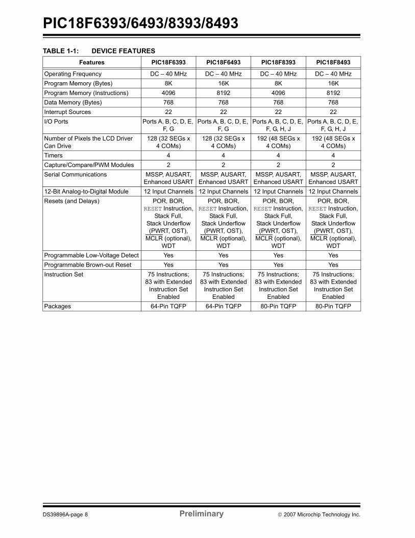
TABLE 1-1: DEVICE FEATURES Features PIC18F6393 PIC18F6493 PIC18F8393 PIC18F8493
Operating Frequency DC � 40 MHz DC � 40 MHz DC � 40 MHz DC � 40 MHzProgram Memory (Bytes) 8K 16K 8K 16KProgram Memory (Instructions) 4096 8192 4096 8192Data Memory (Bytes) 768 768 768 768Interrupt Sources 22 22 22 22I/O Ports Ports A, B, C, D, E,
F, GPorts A, B, C, D, E,
F, GPorts A, B, C, D, E,
F, G, H, JPorts A, B, C, D, E,
F, G, H, JNumber of Pixels the LCD Driver Can Drive
128 (32 SEGs x 4 COMs)
128 (32 SEGs x 4 COMs)
192 (48 SEGs x 4 COMs)
192 (48 SEGs x 4 COMs)
Timers 4 4 4 4Capture/Compare/PWM Modules 2 2 2 2Serial Communications MSSP, AUSART,
Enhanced USARTMSSP, AUSART,
Enhanced USARTMSSP, AUSART,
Enhanced USARTMSSP, AUSART,
Enhanced USART12-Bit Analog-to-Digital Module 12 Input Channels 12 Input Channels 12 Input Channels 12 Input ChannelsResets (and Delays) POR, BOR,
RESET Instruction, Stack Full,
Stack Underflow (PWRT, OST),
MCLR (optional), WDT
POR, BOR, RESET Instruction,
Stack Full, Stack Underflow (PWRT, OST),
MCLR (optional), WDT
POR, BOR, RESET Instruction,
Stack Full, Stack Underflow (PWRT, OST),
MCLR (optional), WDT
POR, BOR, RESET Instruction,
Stack Full, Stack Underflow (PWRT, OST),
MCLR (optional), WDT
Programmable Low-Voltage Detect Yes Yes Yes YesProgrammable Brown-out Reset Yes Yes Yes YesInstruction Set 75 Instructions;
83 with Extended Instruction Set
Enabled
75 Instructions; 83 with Extended
Instruction Set Enabled
75 Instructions; 83 with Extended
Instruction Set Enabled
75 Instructions; 83 with Extended
Instruction Set Enabled
Packages 64-Pin TQFP 64-Pin TQFP 80-Pin TQFP 80-Pin TQFP

© 2007 Microchip Technology Inc. Preliminary DS39896A-page 9
PIC18F6393/6493/8393/8493FIGURE 1-1: PIC18F6X93 (64-PIN) BLOCK DIAGRAM
InstructionDecode and
Control
PORTA
PORTB
PORTC
RA4/T0CKI/SEG14RA5/AN4/HLVDIN/SEG15
RB0/INT0
RC0/T1OSO/T13CKIRC1/T1OSI/CCP2(1)
RC2/CCP1/SEG13RC3/SCK/SCLRC4/SDI/SDARC5/SDO/SEG12RC6/TX1/CK1RC7/RX1/DT1
RA3/AN3/VREF+/SEG17RA2/AN2/VREF-/SEG16RA1/AN1RA0/AN0
RB1/INT1/SEG8
Data Latch
Data Memory(3.9 Kbytes)
Address Latch
Data Address<12>12
AccessBSR FSR0FSR1FSR2
inc/declogic
Address
4 12 4
PCH PCL
PCLATH
8
31 Level Stack
Program Counter
PRODLPRODH
8 x 8 Multiply
8
BITOP88
ALU<8>
Address Latch
Program Memory(48/64 Kbytes)
Data Latch
20
8
8
Table Pointer<21>
inc/dec logic
21
8
Data Bus<8>
Table Latch8
IR
12
3
RB2/INT2/SEG9RB3/INT3/SEG10
PCLATU
PCU
PORTD
RD7/SEG7:RD0/SEG0
OSC2/CLKO(3)/RA6
Note 1: CCP2 is multiplexed with RC1 when Configuration bit, CCP2MX, is set, or RE7 when CCP2MX is not set.2: RG5 is only available when MCLR functionality is disabled.3: OSC1/CLKI and OSC2/CLKO are only available in select oscillator modes and when these pins are not being used as digital I/O.
For additional information, see Section 2.0 �Oscillator Configurations� of the �PIC18F6390/6490/8390/8490 Data Sheet� (DS39629).
RB4/KBI0/SEG11RB5/KBI1RB6/KBI2/PGCRB7/KBI3/PGD
EUSART1Comparators MSSP
Timer2Timer1 Timer3Timer0HLVD
CCP1
BOR ADC12-Bit
W
Instruction Bus <16>
STKPTR Bank
8
State MachineControl Signals
Decode
8
8Power-up
TimerOscillator
Start-up TimerPower-on
ResetWatchdog
Timer
OSC1(3)
OSC2(3)
VDD,
Brown-outReset
InternalOscillator
Fail-SafeClock Monitor
Precision
ReferenceBand Gap
VSS
MCLR(2)
Block
INTRCOscillator
8 MHzOscillator
Single-SupplyProgramming
In-CircuitDebugger
T1OSI
T1OSO
OSC1/CLKI(3)/RA7
PORTELCDBIAS1LCDBIAS2LCDBIAS3COM0RE4/COM1RE5/COM2RE6/COM3RE7/CCP2(1)/SEG31
PORTFRF0/AN5/SEG18RF1/AN6/C2OUT/SEG19RF2/AN7/C1OUT/SEG20RF3/AN8/SEG21RF4/AN9/SEG22RF5/AN10/CVREF/SEG23RF6/AN11/SEG24RF7/SS/SEG25
PORTGRG0/SEG30RG1/TX2/CK2/SEG29RG2/RX2/DT2/SEG28RG3/SEG27RG4/SEG26MCLR/VPP/RG5(2)
AUSART2CCP2 LCDDriver
ROM Latch

PIC18F6393/6493/8393/8493
DS39896A-page 10 Preliminary © 2007 Microchip Technology Inc.
FIGURE 1-2: PIC18F8X93 (80-PIN) BLOCK DIAGRAM
InstructionDecode and
Control
Data Latch
Data Memory(3.9 Kbytes)
Address Latch
Data Address<12>12
AccessBSR FSR0FSR1FSR2
inc/declogic
Address
4 12 4
PCH PCL
PCLATH
8
31 Level Stack
Program Counter
PRODLPRODH
8 x 8 Multiply
8
BITOP88
ALU<8>
Address Latch
Program Memory(48/64 Kbytes)
Data Latch
20
8
8
Table Pointer<21>
inc/dec logic
21
8
Data Bus<8>
Table Latch8
IR
12
3
ROM Latch
PCLATU
PCU
Note 1: CCP2 is multiplexed with RC1 when Configuration bit, CCP2MX, is set and RE7 when CCP2MX is not set.2: RG5 is only available when MCLR functionality is disabled.3: OSC1/CLKI and OSC2/CLKO are only available in select oscillator modes and when these pins are not being used as digital I/O.
For additional information, see Section 2.0 �Oscillator Configurations� of the �PIC18F6390/6490/8390/8490 Data Sheet� (DS39629).
EUSART1Comparators MSSP
Timer2Timer1 Timer3Timer0HLVD
CCP1
BOR ADC12-Bit
W
Instruction Bus <16>
STKPTR Bank
8
State MachineControl Signals
Decode
8
8Power-up
TimerOscillator
Start-up TimerPower-on
ResetWatchdog
Timer
OSC1(3)
OSC2(3)
VDD,
Brown-outReset
InternalOscillator
Fail-SafeClock Monitor
Precision
ReferenceBand Gap
VSS
MCLR(2)
Block
INTRCOscillator
8 MHzOscillator
Single-SupplyProgramming
In-CircuitDebugger
T1OSI
T1OSO
AUSART2CCP2
PORTH
RH7/SEG40:RH4/SEG43
RH3/SEG47:RH0/SEG44
LCDDriver
PORTA
PORTB
PORTC
RA4/T0CKI/SEG14RA5/AN4/HLVDIN/SEG15
RB0/INT0
RC0/T1OSO/T13CKIRC1/T1OSI/CCP2(1)
RC2/CCP1/SEG13RC3/SCK/SCLRC4/SDI/SDARC5/SDO/SEG12RC6/TX1/CK1RC7/RX1/DT1
RA3/AN3/VREF+/SEG17RA2/AN2/VREF-/SEG16RA1/AN1RA0/AN0
RB1/INT1/SEG8RB2/INT2/SEG9RB3/INT3/SEG10
PORTD
RD7/SEG7:RD0/SEG0
OSC2/CLKO(3)/RA6
RB4/KBI0/SEG11RB5/KBI1RB6/KBI2/PGCRB7/KBI3/PGD
OSC1/CLKI(3)/RA7
PORTELCDBIAS1LCDBIAS2LCDBIAS3COM0RE4/COM1RE5/COM2RE6/COM3RE7/CCP2(1)/SEG31
PORTFRF0/AN5/SEG18RF1/AN6/C2OUT/SEG19RF2/AN7/C1OUT/SEG20RF3/AN8/SEG21RF4/AN9/SEG22RF5/AN10/CVREF/SEG23RF6/AN11/SEG24RF7/SS/SEG25
PORTGRG0/SEG30RG1/TX2/CK2/SEG29RG2/RX2/DT2/SEG28RG3/SEG27RG4/SEG26MCLR/VPP/RG5(2)
PORTJ
RJ7/SEG36:RJ4/SEG39
RJ3/SEG35:RJ0/SEG32

© 2007 Microchip Technology Inc. Preliminary DS39896A-page 11
PIC18F6393/6493/8393/8493
TABLE 1-2: PIC18F6X93 PINOUT I/O DESCRIPTIONS
Pin NamePin Number Pin
TypeBufferType Description
TQFP
MCLR/VPP/RG5MCLR
VPPRG5
7I
PI
ST
ST
Master Clear (input) or programming voltage (input).Master Clear (Reset) input. This pin is an active-low Reset to the device.Programming voltage input.Digital input.
OSC1/CLKI/RA7OSC1
CLKI
RA7
39I
I
I/O
ST
CMOS
TTL
Oscillator crystal or external clock input.Oscillator crystal input or external clock source input. ST buffer when configured in RC mode; CMOS otherwise.External clock source input. Always associated with pin function OSC1. (See related OSC1/CLKI, OSC2/CLKO pins.)General purpose I/O pin.
OSC2/CLKO/RA6OSC2
CLKO
RA6
40O
O
I/O
�
�
TTL
Oscillator crystal or clock output.Oscillator crystal output. Connects to crystal or resonator in Crystal Oscillator mode.In RC mode, OSC2 pin outputs CLKO, which has 1/4 the frequency of OSC1 and denotes theinstruction cycle rate. General purpose I/O pin.
Legend: TTL = TTL compatible input CMOS = CMOS compatible input or output ST = Schmitt Trigger input with CMOS levels Analog = Analog input I = Input O = Output P = Power OD = Open-Drain (no P diode to VDD)
Note 1: Default assignment for CCP2 when Configuration bit, CCP2MX, is set.2: Alternate assignment for CCP2 when Configuration bit, CCP2MX, is cleared.

PIC18F6393/6493/8393/8493
DS39896A-page 12 Preliminary © 2007 Microchip Technology Inc.
PORTA is a bidirectional I/O port.
RA0/AN0RA0AN0
24I/OI
TTLAnalog
Digital I/O.Analog input 0.
RA1/AN1RA1AN1
23I/OI
TTLAnalog
Digital I/O.Analog input 1.
RA2/AN2/VREF-/SEG16RA2AN2VREF-SEG16
22I/OIIO
TTLAnalogAnalogAnalog
Digital I/O.Analog input 2.A/D reference voltage (Low) input.SEG16 output for LCD.
RA3/AN3/VREF+/SEG17RA3AN3VREF+SEG17
21I/OIIO
TTLAnalogAnalogAnalog
Digital I/O.Analog input 3.A/D reference voltage (High) input.SEG17 output for LCD.
RA4/T0CKI/SEG14RA4T0CKISEG14
28I/OIO
ST/ODST
Analog
Digital I/O. Open-drain when configured as output.Timer0 external clock input.SEG14 output for LCD.
RA5/AN4/HLVDIN/SEG15RA5AN4HLVDINSEG15
27I/OIIO
TTLAnalogAnalogAnalog
Digital I/O.Analog input 4. Low-Voltage Detect input.SEG15 output for LCD.
RA6 See the OSC2/CLKO/RA6 pin.
RA7 See the OSC1/CLKI/RA7 pin.
TABLE 1-2: PIC18F6X93 PINOUT I/O DESCRIPTIONS (CONTINUED)
Pin NamePin Number Pin
TypeBufferType Description
TQFP
Legend: TTL = TTL compatible input CMOS = CMOS compatible input or output ST = Schmitt Trigger input with CMOS levels Analog = Analog input I = Input O = Output P = Power OD = Open-Drain (no P diode to VDD)
Note 1: Default assignment for CCP2 when Configuration bit, CCP2MX, is set.2: Alternate assignment for CCP2 when Configuration bit, CCP2MX, is cleared.
© 2007 Microchip Technology Inc. Preliminary DS39896A-page 13
PIC18F6393/6493/8393/8493
PORTB is a bidirectional I/O port. PORTB can be software programmed for internal weak pull-ups on all inputs.
RB0/INT0RB0INT0
48I/OI
TTLST
Digital I/O.External interrupt 0.
RB1/INT1/SEG8RB1INT1SEG8
47I/OIO
TTLST
Analog
Digital I/O.External interrupt 1.SEG8 output for LCD.
RB2/INT2/SEG9RB2INT2SEG9
46I/OIO
TTLST
Analog
Digital I/O.External interrupt 2.SEG9 output for LCD.
RB3/INT3/SEG10RB3INT3SEG10
45I/OIO
TTLST
Analog
Digital I/O.External interrupt 3.SEG10 output for LCD.
RB4/KBI0/SEG11RB4KBI0SEG11
44I/OIO
TTLTTL
Analog
Digital I/O.Interrupt-on-change pin.SEG11 output for LCD.
RB5/KBI1RB5KBI1
43I/OI
TTLTTL
Digital I/O.Interrupt-on-change pin.
RB6/KBI2/PGCRB6KBI2PGC
42I/OI
I/O
TTLTTLST
Digital I/O.Interrupt-on-change pin. In-Circuit Debugger and ICSP� programming clock pin.
RB7/KBI3/PGDRB7KBI3PGD
37I/OI
I/O
TTLTTLST
Digital I/O.Interrupt-on-change pin. In-Circuit Debugger and ICSP programming data pin.
TABLE 1-2: PIC18F6X93 PINOUT I/O DESCRIPTIONS (CONTINUED)
Pin NamePin Number Pin
TypeBufferType Description
TQFP
Legend: TTL = TTL compatible input CMOS = CMOS compatible input or output ST = Schmitt Trigger input with CMOS levels Analog = Analog input I = Input O = Output P = Power OD = Open-Drain (no P diode to VDD)
Note 1: Default assignment for CCP2 when Configuration bit, CCP2MX, is set.2: Alternate assignment for CCP2 when Configuration bit, CCP2MX, is cleared.

PIC18F6393/6493/8393/8493
DS39896A-page 14 Preliminary © 2007 Microchip Technology Inc.
PORTC is a bidirectional I/O port.
RC0/T1OSO/T13CKIRC0T1OSOT13CKI
30I/OOI
ST�ST
Digital I/O.Timer1 oscillator output. Timer1/Timer3 external clock input.
RC1/T1OSI/CCP2RC1T1OSICCP2(1)
29I/OI
I/O
STCMOS
ST
Digital I/O.Timer1 oscillator input.Capture 2 input/Compare 2 output/PWM2 output.
RC2/CCP1/SEG13RC2CCP1SEG13
33I/OI/OO
STST
Analog
Digital I/O.Capture 1 input/Compare 1 output/PWM1 output.SEG13 output for LCD.
RC3/SCK/SCLRC3SCKSCL
34I/OI/OI/O
STSTST
Digital I/O.Synchronous serial clock input/output for SPI mode.Synchronous serial clock input/output for I2C� mode.
RC4/SDI/SDARC4SDISDA
35I/OI
I/O
STSTST
Digital I/O.SPI data in.I2C data I/O.
RC5/SDO/SEG12RC5SDOSEG12
36I/OOO
ST�
Analog
Digital I/O.SPI data out.SEG12 output for LCD.
RC6/TX1/CK1RC6TX1CK1
31I/OOI/O
ST�ST
Digital I/O.EUSART1 asynchronous transmit. EUSART1 synchronous clock (see related RX1/DT1).
RC7/RX1/DT1RC7RX1DT1
32I/OI
I/O
STSTST
Digital I/O.EUSART1 asynchronous receive.EUSART1 synchronous data (see related TX1/CK1).
TABLE 1-2: PIC18F6X93 PINOUT I/O DESCRIPTIONS (CONTINUED)
Pin NamePin Number Pin
TypeBufferType Description
TQFP
Legend: TTL = TTL compatible input CMOS = CMOS compatible input or output ST = Schmitt Trigger input with CMOS levels Analog = Analog input I = Input O = Output P = Power OD = Open-Drain (no P diode to VDD)
Note 1: Default assignment for CCP2 when Configuration bit, CCP2MX, is set.2: Alternate assignment for CCP2 when Configuration bit, CCP2MX, is cleared.
© 2007 Microchip Technology Inc. Preliminary DS39896A-page 15
PIC18F6393/6493/8393/8493
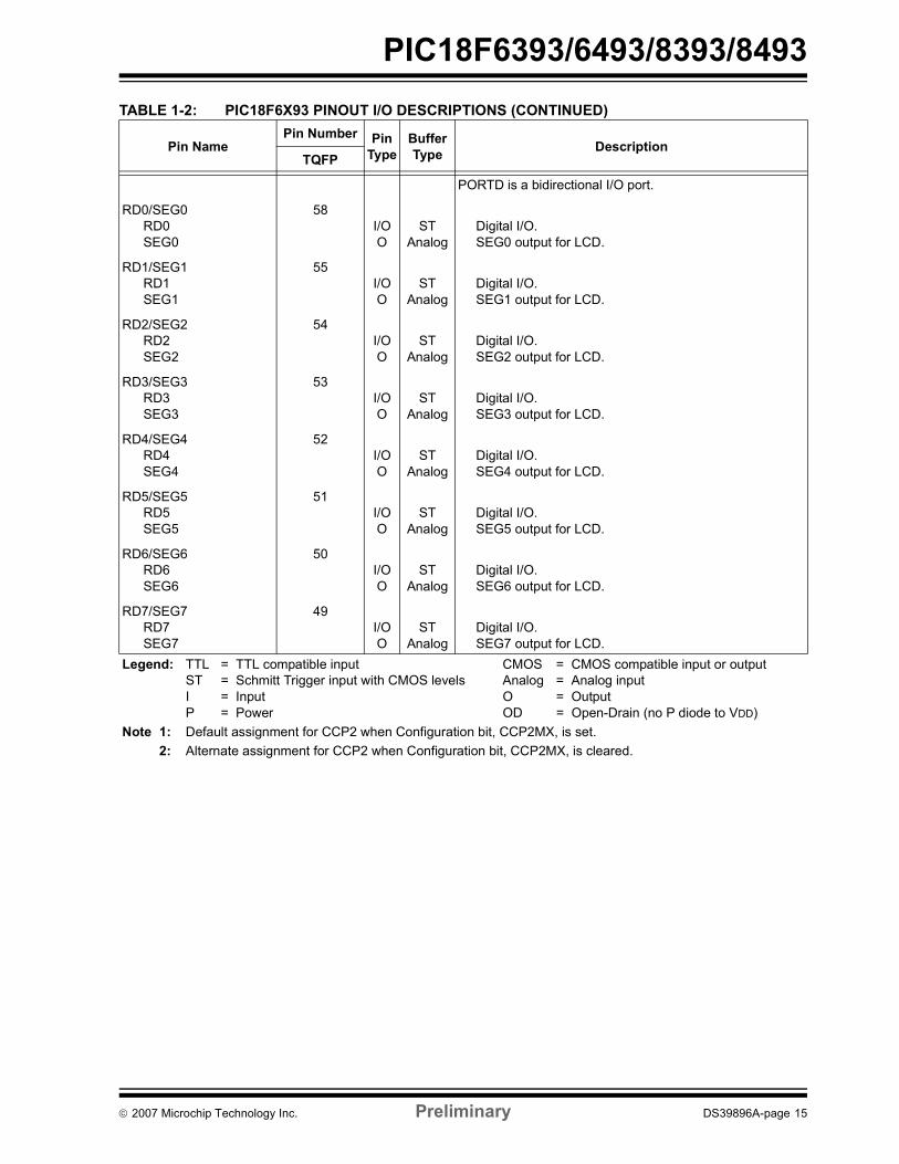
PORTD is a bidirectional I/O port.
RD0/SEG0RD0SEG0
58I/OO
STAnalog
Digital I/O.SEG0 output for LCD.
RD1/SEG1RD1SEG1
55I/OO
STAnalog
Digital I/O.SEG1 output for LCD.
RD2/SEG2RD2SEG2
54I/OO
STAnalog
Digital I/O.SEG2 output for LCD.
RD3/SEG3RD3SEG3
53I/OO
STAnalog
Digital I/O.SEG3 output for LCD.
RD4/SEG4RD4SEG4
52I/OO
STAnalog
Digital I/O.SEG4 output for LCD.
RD5/SEG5RD5SEG5
51I/OO
STAnalog
Digital I/O.SEG5 output for LCD.
RD6/SEG6RD6SEG6
50I/OO
STAnalog
Digital I/O.SEG6 output for LCD.
RD7/SEG7RD7SEG7
49I/OO
STAnalog
Digital I/O.SEG7 output for LCD.
TABLE 1-2: PIC18F6X93 PINOUT I/O DESCRIPTIONS (CONTINUED)
Pin NamePin Number Pin
TypeBufferType Description
TQFP
Legend: TTL = TTL compatible input CMOS = CMOS compatible input or output ST = Schmitt Trigger input with CMOS levels Analog = Analog input I = Input O = Output P = Power OD = Open-Drain (no P diode to VDD)
Note 1: Default assignment for CCP2 when Configuration bit, CCP2MX, is set.2: Alternate assignment for CCP2 when Configuration bit, CCP2MX, is cleared.

PIC18F6393/6493/8393/8493
DS39896A-page 16 Preliminary © 2007 Microchip Technology Inc.
PORTE is a bidirectional I/O port.
LCDBIAS1LCDBIAS1
2I Analog BIAS1 input for LCD.
LCDBIAS2LCDBIAS2
1I Analog BIAS2 input for LCD.
LCDBIAS3LCDBIAS3
64I Analog BIAS3 input for LCD.
COM0COM0
63O Analog COM0 output for LCD.
RE4/COM1RE4COM1
62I/OO
STAnalog
Digital I/O.COM1 output for LCD.
RE5/COM2RE5COM2
61I/OO
STAnalog
Digital I/O.COM2 output for LCD.
RE6/COM3RE6COM3
60I/OO
STAnalog
Digital I/O.COM3 output for LCD.
RE7/CCP2/SEG31RE7CCP2(2)
SEG31
59I/OI/OO
STST
Analog
Digital I/O.Capture 2 input/Compare 2 output/PWM2 output.SEG31 output for LCD.
TABLE 1-2: PIC18F6X93 PINOUT I/O DESCRIPTIONS (CONTINUED)
Pin NamePin Number Pin
TypeBufferType Description
TQFP
Legend: TTL = TTL compatible input CMOS = CMOS compatible input or output ST = Schmitt Trigger input with CMOS levels Analog = Analog input I = Input O = Output P = Power OD = Open-Drain (no P diode to VDD)
Note 1: Default assignment for CCP2 when Configuration bit, CCP2MX, is set.2: Alternate assignment for CCP2 when Configuration bit, CCP2MX, is cleared.
© 2007 Microchip Technology Inc. Preliminary DS39896A-page 17
PIC18F6393/6493/8393/8493
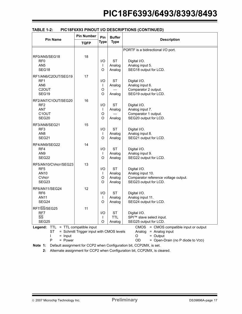
PORTF is a bidirectional I/O port.
RF0/AN5/SEG18RF0AN5SEG18
18I/OIO
STAnalogAnalog
Digital I/O.Analog input 5.SEG18 output for LCD.
RF1/AN6/C2OUT/SEG19RF1AN6C2OUTSEG19
17I/OIOO
STAnalog
�Analog
Digital I/O.Analog input 6.Comparator 2 output.SEG19 output for LCD.
RF2/AN7/C1OUT/SEG20RF2AN7C1OUTSEG20
16I/OIOO
STAnalog
�Analog
Digital I/O.Analog input 7.Comparator 1 output.SEG20 output for LCD.
RF3/AN8/SEG21RF3AN8SEG21
15I/OIO
STAnalogAnalog
Digital I/O.Analog input 8.SEG21 output for LCD.
RF4/AN9/SEG22RF4AN9SEG22
14I/OIO
STAnalogAnalog
Digital I/O.Analog input 9.SEG22 output for LCD.
RF5/AN10/CVREF/SEG23RF5AN10CVREFSEG23
13I/OIOO
STAnalogAnalogAnalog
Digital I/O.Analog input 10. Comparator reference voltage output.SEG23 output for LCD.
RF6/AN11/SEG24RF6AN11SEG24
12I/OIO
STAnalogAnalog
Digital I/O.Analog input 11.SEG24 output for LCD.
RF7/SS/SEG25RF7SSSEG25
11I/OIO
STTTL
Analog
Digital I/O.SPI� slave select input.SEG25 output for LCD.
TABLE 1-2: PIC18F6X93 PINOUT I/O DESCRIPTIONS (CONTINUED)
Pin NamePin Number Pin
TypeBufferType Description
TQFP
Legend: TTL = TTL compatible input CMOS = CMOS compatible input or output ST = Schmitt Trigger input with CMOS levels Analog = Analog input I = Input O = Output P = Power OD = Open-Drain (no P diode to VDD)
Note 1: Default assignment for CCP2 when Configuration bit, CCP2MX, is set.2: Alternate assignment for CCP2 when Configuration bit, CCP2MX, is cleared.
PIC18F6393/6493/8393/8493
DS39896A-page 18 Preliminary © 2007 Microchip Technology Inc.
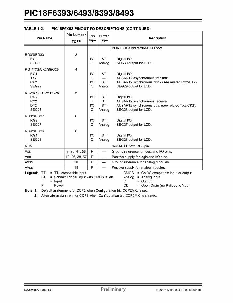
PORTG is a bidirectional I/O port.
RG0/SEG30RG0SEG30
3I/OO
STAnalog
Digital I/O.SEG30 output for LCD.
RG1/TX2/CK2/SEG29RG1TX2CK2SEG29
4I/OOI/OO
ST�ST
Analog
Digital I/O.AUSART2 asynchronous transmit. AUSART2 synchronous clock (see related RX2/DT2).SEG29 output for LCD.
RG2/RX2/DT2/SEG28RG2RX2DT2SEG28
5I/OI
I/OO
STSTST
Analog
Digital I/O.AUSART2 asynchronous receive.AUSART2 synchronous data (see related TX2/CK2).SEG28 output for LCD.
RG3/SEG27RG3SEG27
6I/OO
STAnalog
Digital I/O.SEG27 output for LCD.
RG4/SEG26RG4SEG26
8I/OO
STAnalog
Digital I/O.SEG26 output for LCD.
RG5 See MCLR/VPP/RG5 pin.VSS 9, 25, 41, 56 P � Ground reference for logic and I/O pins.VDD 10, 26, 38, 57 P � Positive supply for logic and I/O pins.AVSS 20 P � Ground reference for analog modules.AVDD 19 P � Positive supply for analog modules.
TABLE 1-2: PIC18F6X93 PINOUT I/O DESCRIPTIONS (CONTINUED)
Pin NamePin Number Pin
TypeBufferType Description
TQFP
Legend: TTL = TTL compatible input CMOS = CMOS compatible input or output ST = Schmitt Trigger input with CMOS levels Analog = Analog input I = Input O = Output P = Power OD = Open-Drain (no P diode to VDD)
Note 1: Default assignment for CCP2 when Configuration bit, CCP2MX, is set.2: Alternate assignment for CCP2 when Configuration bit, CCP2MX, is cleared.

© 2007 Microchip Technology Inc. Preliminary DS39896A-page 19
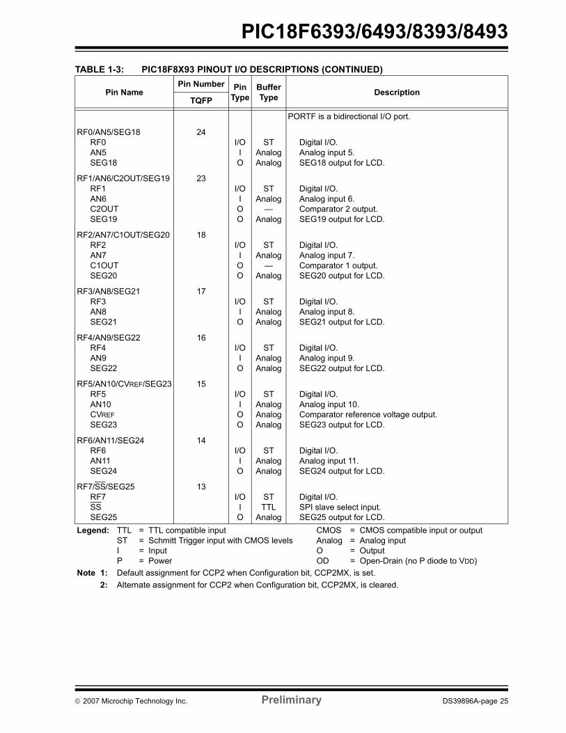
PIC18F6393/6493/8393/8493TABLE 1-3: PIC18F8X93 PINOUT I/O DESCRIPTIONS
Pin NamePin Number Pin
TypeBufferType Description
TQFP
MCLR/VPP/RG5MCLR
VPPRG5
9I
PI
ST
ST
Master Clear (input) or programming voltage (input).Master Clear (Reset) input. This pin is an active-low Reset to the device.Programming voltage input.Digital input.
OSC1/CLKI/RA7OSC1
CLKI
RA7
49I
I
I/O
ST
CMOS
TTL
Oscillator crystal or external clock input.Oscillator crystal input or external clock source input. ST buffer when configured in RC mode; CMOS otherwise.External clock source input. Always associated with pin function OSC1. (See related OSC1/CLKI, OSC2/CLKO pins.)General purpose I/O pin.
OSC2/CLKO/RA6OSC2
CLKO
RA6
50O
O
I/O
�
�
TTL
Oscillator crystal or clock output.Oscillator crystal output. Connects to crystal or resonator in Crystal Oscillator mode.In RC mode, OSC2 pin outputs CLKO, which has 1/4 the frequency of OSC1 and denotes theinstruction cycle rate. General purpose I/O pin.
Legend: TTL = TTL compatible input CMOS = CMOS compatible input or output ST = Schmitt Trigger input with CMOS levels Analog = Analog input I = Input O = Output P = Power OD = Open-Drain (no P diode to VDD)
Note 1: Default assignment for CCP2 when Configuration bit, CCP2MX, is set.2: Alternate assignment for CCP2 when Configuration bit, CCP2MX, is cleared.

PIC18F6393/6493/8393/8493
DS39896A-page 20 Preliminary © 2007 Microchip Technology Inc.
PORTA is a bidirectional I/O port.
RA0/AN0RA0AN0
30I/OI
TTLAnalog
Digital I/O.Analog input 0.
RA1/AN1RA1AN1
29I/OI
TTLAnalog
Digital I/O.Analog input 1.
RA2/AN2/VREF-/SEG16RA2AN2VREF-SEG16
28I/OIIO
TTLAnalogAnalogAnalog
Digital I/O.Analog input 2.A/D reference voltage (Low) input.SEG16 output for LCD.
RA3/AN3/VREF+/SEG17RA3AN3VREF+SEG17
27I/OIIO
TTLAnalogAnalogAnalog
Digital I/O.Analog input 3.A/D reference voltage (High) input.SEG17 output for LCD.
RA4/T0CKI/SEG14RA4T0CKISEG14
34I/OIO
ST/ODST
Analog
Digital I/O. Open-drain when configured as output.Timer0 external clock input.SEG14 output for LCD.
RA5/AN4/HLVDIN/SEG15RA5AN4HLVDINSEG15
33I/OIIO
TTLAnalogAnalogAnalog
Digital I/O.Analog input 4. Low-Voltage Detect input.SEG15 output for LCD.
RA6 See the OSC2/CLKO/RA6 pin.
RA7 See the OSC1/CLKI/RA7 pin.
TABLE 1-3: PIC18F8X93 PINOUT I/O DESCRIPTIONS (CONTINUED)
Pin NamePin Number Pin
TypeBufferType Description
TQFP
Legend: TTL = TTL compatible input CMOS = CMOS compatible input or output ST = Schmitt Trigger input with CMOS levels Analog = Analog input I = Input O = Output P = Power OD = Open-Drain (no P diode to VDD)
Note 1: Default assignment for CCP2 when Configuration bit, CCP2MX, is set.2: Alternate assignment for CCP2 when Configuration bit, CCP2MX, is cleared.

© 2007 Microchip Technology Inc. Preliminary DS39896A-page 21
PIC18F6393/6493/8393/8493
PORTB is a bidirectional I/O port. PORTB can be software programmed for internal weak pull-ups on all inputs.
RB0/INT0RB0INT0
58I/OI
TTLST
Digital I/O.External interrupt 0.
RB1/INT1/SEG8RB1INT1SEG8
57I/OIO
TTLST
Analog
Digital I/O.External interrupt 1.SEG8 output for LCD.
RB2/INT2/SEG9RB2INT2SEG9
56I/OIO
TTLST
Analog
Digital I/O.External interrupt 2.SEG9 output for LCD.
RB3/INT3/SEG10RB3INT3SEG10
55I/OIO
TTLST
Analog
Digital I/O.External interrupt 3.SEG10 output for LCD.
RB4/KBI0/SEG11RB4KBI0SEG11
54I/OIO
TTLTTL
Analog
Digital I/O.Interrupt-on-change pin.SEG11 output for LCD.
RB5/KBI1RB5KBI1
53I/OI
TTLTTL
Digital I/O.Interrupt-on-change pin.
RB6/KBI2/PGCRB6KBI2PGC
52I/OI
I/O
TTLTTLST
Digital I/O.Interrupt-on-change pin. In-Circuit Debugger and ICSP� programming clock pin.
RB7/KBI3/PGDRB7KBI3PGD
47I/OI
I/O
TTLTTLST
Digital I/O.Interrupt-on-change pin. In-Circuit Debugger and ICSP programming data pin.
TABLE 1-3: PIC18F8X93 PINOUT I/O DESCRIPTIONS (CONTINUED)
Pin NamePin Number Pin
TypeBufferType Description
TQFP
Legend: TTL = TTL compatible input CMOS = CMOS compatible input or output ST = Schmitt Trigger input with CMOS levels Analog = Analog input I = Input O = Output P = Power OD = Open-Drain (no P diode to VDD)
Note 1: Default assignment for CCP2 when Configuration bit, CCP2MX, is set.2: Alternate assignment for CCP2 when Configuration bit, CCP2MX, is cleared.
PIC18F6393/6493/8393/8493
DS39896A-page 22 Preliminary © 2007 Microchip Technology Inc.
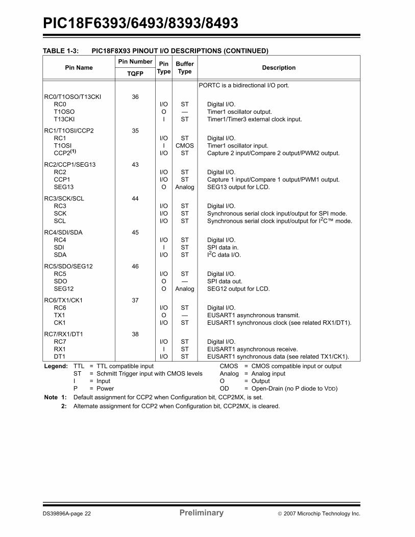
PORTC is a bidirectional I/O port.
RC0/T1OSO/T13CKIRC0T1OSOT13CKI
36I/OOI
ST�ST
Digital I/O.Timer1 oscillator output. Timer1/Timer3 external clock input.
RC1/T1OSI/CCP2RC1T1OSICCP2(1)
35I/OI
I/O
STCMOS
ST
Digital I/O.Timer1 oscillator input.Capture 2 input/Compare 2 output/PWM2 output.
RC2/CCP1/SEG13RC2CCP1SEG13
43I/OI/OO
STST
Analog
Digital I/O.Capture 1 input/Compare 1 output/PWM1 output.SEG13 output for LCD.
RC3/SCK/SCLRC3SCKSCL
44I/OI/OI/O
STSTST
Digital I/O.Synchronous serial clock input/output for SPI mode.Synchronous serial clock input/output for I2C� mode.
RC4/SDI/SDARC4SDISDA
45I/OI
I/O
STSTST
Digital I/O.SPI data in.I2C data I/O.
RC5/SDO/SEG12RC5SDOSEG12
46I/OOO
ST�
Analog
Digital I/O.SPI data out.SEG12 output for LCD.
RC6/TX1/CK1RC6TX1CK1
37I/OO
I/O
ST�ST
Digital I/O.EUSART1 asynchronous transmit. EUSART1 synchronous clock (see related RX1/DT1).
RC7/RX1/DT1RC7RX1DT1
38I/OI
I/O
STSTST
Digital I/O.EUSART1 asynchronous receive.EUSART1 synchronous data (see related TX1/CK1).
TABLE 1-3: PIC18F8X93 PINOUT I/O DESCRIPTIONS (CONTINUED)
Pin NamePin Number Pin
TypeBufferType Description
TQFP
Legend: TTL = TTL compatible input CMOS = CMOS compatible input or output ST = Schmitt Trigger input with CMOS levels Analog = Analog input I = Input O = Output P = Power OD = Open-Drain (no P diode to VDD)
Note 1: Default assignment for CCP2 when Configuration bit, CCP2MX, is set.2: Alternate assignment for CCP2 when Configuration bit, CCP2MX, is cleared.

© 2007 Microchip Technology Inc. Preliminary DS39896A-page 23
PIC18F6393/6493/8393/8493
PORTD is a bidirectional I/O port.
RD0/SEG0RD0SEG0
72I/OO
STAnalog
Digital I/O.SEG0 output for LCD.
RD1/SEG1RD1SEG1
69I/OO
STAnalog
Digital I/O.SEG1 output for LCD.
RD2/SEG2RD2SEG2
68I/OO
STAnalog
Digital I/O.SEG2 output for LCD.
RD3/SEG3RD3SEG3
67I/OO
STAnalog
Digital I/O.SEG3 output for LCD.
RD4/SEG4RD4SEG4
66I/OO
STAnalog
Digital I/O.SEG4 output for LCD.
RD5/SEG5RD5SEG5
65I/OO
STAnalog
Digital I/O.SEG5 output for LCD.
RD6/SEG6RD6SEG6
64I/OO
STAnalog
Digital I/O.SEG6 output for LCD.
RD7/SEG7RD7SEG7
63I/OO
STAnalog
Digital I/O.SEG7 output for LCD.
TABLE 1-3: PIC18F8X93 PINOUT I/O DESCRIPTIONS (CONTINUED)
Pin NamePin Number Pin
TypeBufferType Description
TQFP
Legend: TTL = TTL compatible input CMOS = CMOS compatible input or output ST = Schmitt Trigger input with CMOS levels Analog = Analog input I = Input O = Output P = Power OD = Open-Drain (no P diode to VDD)
Note 1: Default assignment for CCP2 when Configuration bit, CCP2MX, is set.2: Alternate assignment for CCP2 when Configuration bit, CCP2MX, is cleared.

PIC18F6393/6493/8393/8493
DS39896A-page 24 Preliminary © 2007 Microchip Technology Inc.
PORTE is a bidirectional I/O port.
LCDBIAS1LCDBIAS1
4I Analog BIAS1 input for LCD.
LCDBIAS2LCDBIAS2
3I Analog BIAS2 input for LCD.
LCDBIAS3LCDBIAS3
78I Analog BIAS3 input for LCD.
COM0COM0
77O Analog COM0 output for LCD.
RE4/COM1RE4COM1
76I/OO
STAnalog
Digital I/O.COM1 output for LCD.
RE5/COM2RE5COM2
75I/OO
STAnalog
Digital I/O.COM2 output for LCD.
RE6/COM3RE6COM3
74I/OO
STAnalog
Digital I/O.COM3 output for LCD.
RE7/CCP2/SEG31RE7CCP2(2)
SEG31
73I/OI/OO
STST
Analog
Digital I/O.Capture 2 input/Compare 2 output/PWM2 output.SEG31 output for LCD.
TABLE 1-3: PIC18F8X93 PINOUT I/O DESCRIPTIONS (CONTINUED)
Pin NamePin Number Pin
TypeBufferType Description
TQFP
Legend: TTL = TTL compatible input CMOS = CMOS compatible input or output ST = Schmitt Trigger input with CMOS levels Analog = Analog input I = Input O = Output P = Power OD = Open-Drain (no P diode to VDD)
Note 1: Default assignment for CCP2 when Configuration bit, CCP2MX, is set.2: Alternate assignment for CCP2 when Configuration bit, CCP2MX, is cleared.
© 2007 Microchip Technology Inc. Preliminary DS39896A-page 25
PIC18F6393/6493/8393/8493
PORTF is a bidirectional I/O port.
RF0/AN5/SEG18RF0AN5SEG18
24I/OIO
STAnalogAnalog
Digital I/O.Analog input 5.SEG18 output for LCD.
RF1/AN6/C2OUT/SEG19RF1AN6C2OUTSEG19
23I/OIOO
STAnalog
�Analog
Digital I/O.Analog input 6.Comparator 2 output.SEG19 output for LCD.
RF2/AN7/C1OUT/SEG20RF2AN7C1OUTSEG20
18I/OIOO
STAnalog
�Analog
Digital I/O.Analog input 7.Comparator 1 output.SEG20 output for LCD.
RF3/AN8/SEG21RF3AN8SEG21
17I/OIO
STAnalogAnalog
Digital I/O.Analog input 8.SEG21 output for LCD.
RF4/AN9/SEG22RF4AN9SEG22
16I/OIO
STAnalogAnalog
Digital I/O.Analog input 9.SEG22 output for LCD.
RF5/AN10/CVREF/SEG23RF5AN10CVREFSEG23
15I/OIOO
STAnalogAnalogAnalog
Digital I/O.Analog input 10. Comparator reference voltage output.SEG23 output for LCD.
RF6/AN11/SEG24RF6AN11SEG24
14I/OIO
STAnalogAnalog
Digital I/O.Analog input 11.SEG24 output for LCD.
RF7/SS/SEG25RF7SSSEG25
13I/OIO
STTTL
Analog
Digital I/O.SPI slave select input.SEG25 output for LCD.
TABLE 1-3: PIC18F8X93 PINOUT I/O DESCRIPTIONS (CONTINUED)
Pin NamePin Number Pin
TypeBufferType Description
TQFP
Legend: TTL = TTL compatible input CMOS = CMOS compatible input or output ST = Schmitt Trigger input with CMOS levels Analog = Analog input I = Input O = Output P = Power OD = Open-Drain (no P diode to VDD)
Note 1: Default assignment for CCP2 when Configuration bit, CCP2MX, is set.2: Alternate assignment for CCP2 when Configuration bit, CCP2MX, is cleared.

PIC18F6393/6493/8393/8493
DS39896A-page 26 Preliminary © 2007 Microchip Technology Inc.
PORTG is a bidirectional I/O port.
RG0/SEG30RG0SEG30
5I/OO
STAnalog
Digital I/O.SEG30 output for LCD.
RG1/TX2/CK2/SEG29RG1TX2CK2SEG29
6I/OO
I/OO
ST�ST
Analog
Digital I/O.AUSART2 asynchronous transmit. AUSART2 synchronous clock (see related RX2/DT2).SEG29 output for LCD.
RG2/RX2/DT2/SEG28RG2RX2DT2SEG28
7I/OI
I/OO
STSTST
Analog
Digital I/O.AUSART2 asynchronous receive.AUSART2 synchronous data (see related TX2/CK2).SEG28 output for LCD.
RG3/SEG27RG3SEG27
8I/OO
STAnalog
Digital I/O.SEG27 output for LCD.
RG4/SEG26RG4SEG26
10I/OO
STAnalog
Digital I/O.SEG26 output for LCD.
RG5 See MCLR/VPP/RG5 pin.
TABLE 1-3: PIC18F8X93 PINOUT I/O DESCRIPTIONS (CONTINUED)
Pin NamePin Number Pin
TypeBufferType Description
TQFP
Legend: TTL = TTL compatible input CMOS = CMOS compatible input or output ST = Schmitt Trigger input with CMOS levels Analog = Analog input I = Input O = Output P = Power OD = Open-Drain (no P diode to VDD)
Note 1: Default assignment for CCP2 when Configuration bit, CCP2MX, is set.2: Alternate assignment for CCP2 when Configuration bit, CCP2MX, is cleared.

© 2007 Microchip Technology Inc. Preliminary DS39896A-page 27
PIC18F6393/6493/8393/8493
PORTH is a bidirectional I/O port.
RH0/SEG47RH0SEG47
79I/OO
STAnalog
Digital I/O.SEG47 output for LCD.
RH1/SEG46RH1SEG46
80I/OO
STAnalog
Digital I/O.SEG46 output for LCD.
RH2/SEG45RH2SEG45
1I/OO
STAnalog
Digital I/O.SEG45 output for LCD.
RH3/SEG44RH3SEG44
2I/OO
STAnalog
Digital I/O.SEG44 output for LCD.
RH4/SEG40RH4SEG40
22I/OO
STAnalog
Digital I/O.SEG40 output for LCD.
RH5/SEG41RH5SEG41
21I/OO
STAnalog
Digital I/O.SEG41 output for LCD.
RH6/SEG42RH6SEG42
20I/OO
STAnalog
Digital I/O.SEG42 output for LCD.
RH7/SEG43RH7SEG43
19I/OO
STAnalog
Digital I/O.SEG43 output for LCD.
TABLE 1-3: PIC18F8X93 PINOUT I/O DESCRIPTIONS (CONTINUED)
Pin NamePin Number Pin
TypeBufferType Description
TQFP
Legend: TTL = TTL compatible input CMOS = CMOS compatible input or output ST = Schmitt Trigger input with CMOS levels Analog = Analog input I = Input O = Output P = Power OD = Open-Drain (no P diode to VDD)
Note 1: Default assignment for CCP2 when Configuration bit, CCP2MX, is set.2: Alternate assignment for CCP2 when Configuration bit, CCP2MX, is cleared.
PIC18F6393/6493/8393/8493
DS39896A-page 28 Preliminary © 2007 Microchip Technology Inc.
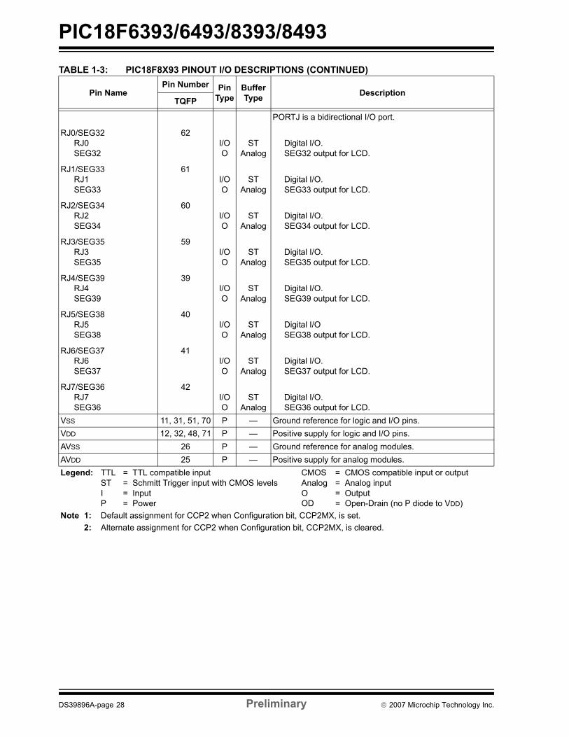
PORTJ is a bidirectional I/O port.
RJ0/SEG32RJ0SEG32
62I/OO
STAnalog
Digital I/O.SEG32 output for LCD.
RJ1/SEG33RJ1SEG33
61I/OO
STAnalog
Digital I/O.SEG33 output for LCD.
RJ2/SEG34RJ2SEG34
60I/OO
STAnalog
Digital I/O.SEG34 output for LCD.
RJ3/SEG35RJ3SEG35
59I/OO
STAnalog
Digital I/O.SEG35 output for LCD.
RJ4/SEG39RJ4SEG39
39I/OO
STAnalog
Digital I/O.SEG39 output for LCD.
RJ5/SEG38RJ5SEG38
40I/OO
STAnalog
Digital I/OSEG38 output for LCD.
RJ6/SEG37RJ6SEG37
41I/OO
STAnalog
Digital I/O.SEG37 output for LCD.
RJ7/SEG36RJ7SEG36
42I/OO
STAnalog
Digital I/O.SEG36 output for LCD.
VSS 11, 31, 51, 70 P � Ground reference for logic and I/O pins.VDD 12, 32, 48, 71 P � Positive supply for logic and I/O pins.AVSS 26 P � Ground reference for analog modules.AVDD 25 P � Positive supply for analog modules.
TABLE 1-3: PIC18F8X93 PINOUT I/O DESCRIPTIONS (CONTINUED)
Pin NamePin Number Pin
TypeBufferType Description
TQFP
Legend: TTL = TTL compatible input CMOS = CMOS compatible input or output ST = Schmitt Trigger input with CMOS levels Analog = Analog input I = Input O = Output P = Power OD = Open-Drain (no P diode to VDD)
Note 1: Default assignment for CCP2 when Configuration bit, CCP2MX, is set.2: Alternate assignment for CCP2 when Configuration bit, CCP2MX, is cleared.

© 2007 Microchip Technology Inc. Preliminary DS39896A-page 29
PIC18F6393/6493/8393/8493
2.0 12-BIT ANALOG-TO-DIGITAL CONVERTER (A/D) MODULE
The Analog-to-Digital (A/D) Converter module convertsan analog input signal to a 12-bit digital number. Themodule has 12 inputs for both PIC18F6393/6493 (64-pin)and PIC18F8393/8493 (80-pin) devices.
The module has five registers:
� A/D Result High Register (ADRESH)� A/D Result Low Register (ADRESL)� A/D Control Register 0 (ADCON0)� A/D Control Register 1 (ADCON1)� A/D Control Register 2 (ADCON2)
The ADCON0 register, shown in Register 2-1, controlsthe operation of the A/D module. The ADCON1register, shown in Register 2-2, configures thefunctions of the port pins. The ADCON2 register,shown in Register 2-3, configures the A/D clocksource, programmed acquisition time and justification.
REGISTER 2-1: ADCON0: A/D CONTROL REGISTER 0
U-0 U-0 R/W-0 R/W-0 R/W-0 R/W-0 R/W-0 R/W-0
� � CHS3 CHS2 CHS1 CHS0 GO/DONE ADONbit 7 bit 0
Legend:R = Readable bit W = Writable bit U = Unimplemented bit, read as �0�-n = Value at POR �1� = Bit is set �0� = Bit is cleared x = Bit is unknown
bit 7-6 Unimplemented: Read as �0�bit 5-2 CHS3:CHS0: Analog Channel Select bits
0000 = Channel 0 (AN0)0001 = Channel 1 (AN1)0010 = Channel 2 (AN2)0011 = Channel 3 (AN3)0100 = Channel 4 (AN4)0101 = Channel 5 (AN5)0110 = Channel 6 (AN6)0111 = Channel 7 (AN7)1000 = Channel 8 (AN8)1001 = Channel 9 (AN9)1010 = Channel 10 (AN10)1011 = Channel 11 (AN11)1100 = Unimplemented(1)
1101 = Unimplemented(1)
1110 = Unimplemented(1)
1111 = Unimplemented(1)
bit 1 GO/DONE: A/D Conversion Status bitWhen ADON = 1: 1 = A/D conversion in progress0 = A/D Idle
bit 0 ADON: A/D On bit1 = A/D Converter module is enabled 0 = A/D Converter module is disabled
Note 1: Performing a conversion on unimplemented channels will return a floating input measurement.
REGISTER 2-2: ADCON1: A/D CONTROL REGISTER 1
U-0 U-0 R/W-0 R/W-0 R/W-0 R/W-0 R/W-0 R/W-0
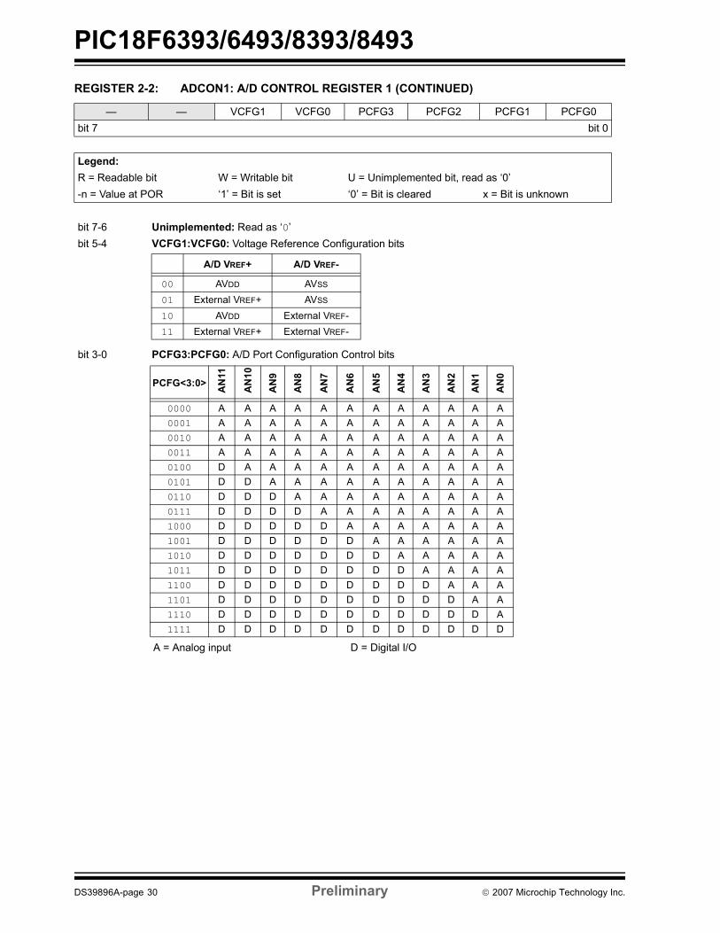
PIC18F6393/6493/8393/8493
DS39896A-page 30 Preliminary © 2007 Microchip Technology Inc.
� � VCFG1 VCFG0 PCFG3 PCFG2 PCFG1 PCFG0bit 7 bit 0
Legend:R = Readable bit W = Writable bit U = Unimplemented bit, read as �0�-n = Value at POR �1� = Bit is set �0� = Bit is cleared x = Bit is unknown
bit 7-6 Unimplemented: Read as �0�bit 5-4 VCFG1:VCFG0: Voltage Reference Configuration bits
bit 3-0 PCFG3:PCFG0: A/D Port Configuration Control bits
REGISTER 2-2: ADCON1: A/D CONTROL REGISTER 1 (CONTINUED)
A/D VREF+ A/D VREF-
00 AVDD AVSS
01 External VREF+ AVSS
10 AVDD External VREF-11 External VREF+ External VREF-
A = Analog input D = Digital I/O
PCFG<3:0> AN
11
AN
10
AN
9
AN
8
AN
7
AN
6
AN
5
AN
4
AN
3
AN
2
AN
1
AN
0
0000 A A A A A A A A A A A A0001 A A A A A A A A A A A A0010 A A A A A A A A A A A A0011 A A A A A A A A A A A A0100 D A A A A A A A A A A A0101 D D A A A A A A A A A A0110 D D D A A A A A A A A A0111 D D D D A A A A A A A A1000 D D D D D A A A A A A A1001 D D D D D D A A A A A A1010 D D D D D D D A A A A A1011 D D D D D D D D A A A A1100 D D D D D D D D D A A A1101 D D D D D D D D D D A A1110 D D D D D D D D D D D A1111 D D D D D D D D D D D D

© 2007 Microchip Technology Inc. Preliminary DS39896A-page 31
PIC18F6393/6493/8393/8493 REGISTER 2-3: ADCON2: A/D CONTROL REGISTER 2
R/W-0 U-0 R/W-0 R/W-0 R/W-0 R/W-0 R/W-0 R/W-0ADFM � ACQT2 ACQT1 ACQT0 ADCS2 ADCS1 ADCS0
bit 7 bit 0
Legend:R = Readable bit W = Writable bit U = Unimplemented bit, read as �0�-n = Value at POR �1� = Bit is set �0� = Bit is cleared x = Bit is unknown
bit 7 ADFM: A/D Result Format Select bit1 = Right justified 0 = Left justified
bit 6 Unimplemented: Read as �0�bit 5-3 ACQT2:ACQT0: A/D Acquisition Time Select bits
111 = 20 TAD110 = 16 TAD101 = 12 TAD100 = 8 TAD011 = 6 TAD010 = 4 TAD001 = 2 TAD000 = 0 TAD(1)
bit 2-0 ADCS2:ADCS0: A/D Conversion Clock Select bits111 = FRC (clock derived from A/D RC oscillator)(1) 110 = FOSC/64 101 = FOSC/16 100 = FOSC/4 011 = FRC (clock derived from A/D RC oscillator)(1) 010 = FOSC/32 001 = FOSC/8 000 = FOSC/2
Note 1: If the A/D FRC clock source is selected, a delay of one TCY (instruction cycle) is added before the A/D clock starts. This allows the SLEEP instruction to be executed before starting a conversion.

PIC18F6393/6493/8393/8493
DS39896A-page 32 Preliminary © 2007 Microchip Technology Inc.
The analog reference voltage is software selectable toeither the device�s positive and negative supply voltage(VDD and VSS), or the voltage level on the RA3/AN3/VREF+/SEG17 and RA2/AN2/VREF-/SEG16 pins.
The A/D Converter has a unique feature of being ableto operate while the device is in Sleep mode. To oper-ate in Sleep, the A/D conversion clock must be derivedfrom the A/D�s internal RC oscillator.
The output of the sample and hold is the input into theconverter, which generates the result via successiveapproximation.
A device Reset forces all registers to their Reset state.This forces the A/D module to be turned off and anyconversion in progress is aborted.
Each port pin associated with the A/D Converter can beconfigured as an analog input or a digital I/O. TheADRESH and ADRESL registers contain the result ofthe A/D conversion. When the A/D conversion is com-plete, the result is loaded into the ADRESH:ADRESLregister pair, the GO/DONE bit (ADCON0<1>) is clearedand the A/D Interrupt Flag bit, ADIF, is set. The blockdiagram of the A/D module is shown in Figure 2-1.
FIGURE 2-1: A/D BLOCK DIAGRAM
(Input Voltage)VAIN
VREF+Reference
Voltage
AVDD(1)
VCFG1:VCFG0
CHS3:CHS0
AN7
AN6
AN5
AN4
AN3
AN2
AN1
AN0
0111
0110
0101
0100
0011
0010
0001
0000
12-BitA/D
VREF-
AVSS(1)
Converter
AN11
AN10
AN9
AN8
1011
1010
1001
1000
Note 1: I/O pins have diode protection to VDD and VSS.
0X1XX1X0

© 2007 Microchip Technology Inc. Preliminary DS39896A-page 33
PIC18F6393/6493/8393/8493The value in the ADRESH:ADRESL registers isunknown following Power-on and Brown-out Resets andis not affected by any other Reset.
After the A/D module has been configured as desired,the selected channel must be acquired before theconversion is started. The analog input channels musthave their corresponding TRIS bits selected as aninput. To determine acquisition time, see Section 2.1�A/D Acquisition Requirements�. After this acquisi-tion time has elapsed, the A/D conversion can bestarted. An acquisition time can be programmed tooccur between setting the GO/DONE bit and the actualstart of the conversion.
The following steps should be followed to perform an A/Dconversion:
1. Configure the A/D module:� Configure analog pins, voltage reference and
digital I/O (ADCON1)� Select A/D input channel (ADCON0)� Select A/D acquisition time (ADCON2)� Select A/D conversion clock (ADCON2)� Turn on A/D module (ADCON0)
2. Configure A/D interrupt (if desired):� Clear ADIF bit � Set ADIE bit � Set GIE bit
3. Wait the required acquisition time (if required).4. Start conversion:
� Set GO/DONE bit (ADCON0<1>)
5. Wait for A/D conversion to complete by either:� Polling for the GO/DONE bit to be cleared
OR
� Waiting for the A/D interrupt6. Read A/D Result registers (ADRESH:ADRESL);
clear bit, ADIF, if required.7. For the next conversion, go to step 1 or step 2,
as required. The A/D conversion time per bit isdefined as TAD. A minimum wait of 2 TAD isrequired before the next acquisition starts.
FIGURE 2-2: A/D TRANSFER FUNCTION
FIGURE 2-3: ANALOG INPUT MODEL
Dig
ital C
ode
Out
put
FFEh
003h
002h
001h
000h0.
5 LS
B
1 LS
B
1.5
LSB
2 LS
B
2.5
LSB
4094
LSB
4094
.5 L
SB
3 LS
B
Analog Input Voltage
FFFh
4095
LSB
4095
.5 L
SBVAIN CPIN
Rs ANx
5 pF
VT = 0.6V
VT = 0.6V ILEAKAGE
RIC ≤ 1k
SamplingSwitch
SS RSS
CHOLD = 25 pF
VSS
VDD
±100 nA
Legend: CPIN
VTILEAKAGE
RIC
SSCHOLD
= Input Capacitance= Threshold Voltage= Leakage Current at the pin due to
= Interconnect Resistance= Sampling Switch= Sample/Hold Capacitance (from DAC)
various junctions
= Sampling Switch ResistanceRSS
VDD
6V
Sampling Switch
5V4V3V2V
1 2 3 4(kΩ)
PIC18F6393/6493/8393/8493
DS39896A-page 34 Preliminary © 2007 Microchip Technology Inc.
2.1 A/D Acquisition RequirementsFor the A/D Converter to meet its specified accuracy,the charge holding capacitor (CHOLD) must be allowedto fully charge to the input channel voltage level. Theanalog input model is shown in Figure 2-3. The sourceimpedance (RS) and the internal sampling switch (RSS)impedance directly affect the time required to chargethe capacitor, CHOLD. The sampling switch (RSS)impedance varies over the device voltage (VDD). Thesource impedance affects the offset voltage at the ana-log input (due to pin leakage current). The maximumrecommended impedance for analog sources is2.5 kΩ. After the analog input channel is selected(changed), the channel must be sampled for at leastthe minimum acquisition time before starting aconversion.
To calculate the minimum acquisition time, Equation 2-1may be used. This equation assumes that 1/2 LSb erroris used (4096 steps for the 12-bit A/D). The 1/2 LSb erroris the maximum error allowed for the A/D to meet itsspecified resolution.
Equation 2-3 shows the calculation of the minimumrequired acquisition time, TACQ. This calculation isbased on the following application systemassumptions:
CHOLD = 25 pF Rs = 2.5 kΩ Conversion Error ≤ 1/2 LSb VDD = 3V → Rss = 4 kΩ Temperature = 85°C (system max.)
EQUATION 2-1: ACQUISITION TIME
EQUATION 2-2: A/D MINIMUM CHARGING TIME
EQUATION 2-3: CALCULATING THE MINIMUM REQUIRED ACQUISITION TIME
Note: When the conversion is started, theholding capacitor is disconnected from theinput pin.
TACQ = Amplifier Settling Time + Holding Capacitor Charging Time + Temperature Coefficient
= TAMP + TC + TCOFF
VHOLD = (VREF � (VREF/4096)) � (1 � e(-TC/CHOLD(RIC + RSS + RS))) or TC = � (CHOLD)(RIC + RSS + RS) ln(1/4096)
TACQ = TAMP + TC + TCOFF
TAMP = 0.2 µs
TCOFF = (Temp � 25°C)(0.02 µs/°C)(85°C � 25°C)(0.02 µs/°C)1.2 µs
Temperature coefficient is only required for temperatures > 25°C. Below 25°C, TCOFF = 0 µs.
TC = -(CHOLD)(RIC + RSS + RS) ln(1/4096) µs-(25 pF) (1 kΩ + 4 kΩ + 2.5 kΩ) ln(0.0002441) µs 1.56 µs
TACQ = 0.2 µs + 1.56 μs + 1.2 µs2.96 µs

© 2007 Microchip Technology Inc. Preliminary DS39896A-page 35
PIC18F6393/6493/8393/84932.2 Selecting and Configuring
Acquisition TimeThe ADCON2 register allows the user to select anacquisition time that occurs each time the GO/DONEbit is set. It also gives users the option to use anautomatically determined acquisition time.
Acquisition time may be set with the ACQT2:ACQT0bits (ADCON2<5:3>), which provide a range of 2 to20 TAD. When the GO/DONE bit is set, the A/D modulecontinues to sample the input for the selected acquisi-tion time, then automatically begins a conversion.Since the acquisition time is programmed, there maybe no need to wait for an acquisition time betweenselecting a channel and setting the GO/DONE bit.
Manual acquisition is selected whenACQT2:ACQT0 = 000. When the GO/DONE bit is set,sampling is stopped and a conversion begins. The useris responsible for ensuring the required acquisition timehas passed between selecting the desired inputchannel and setting the GO/DONE bit. This option isalso the default Reset state of the ACQT2:ACQT0 bitsand is compatible with devices that do not offerprogrammable acquisition times.
In either case, when the conversion is completed, theGO/DONE bit is cleared, the ADIF flag is set and theA/D begins sampling the currently selected channelagain. If an acquisition time is programmed, there isnothing to indicate if the acquisition time has ended orif the conversion has begun.
2.3 Selecting the A/D Conversion Clock
The A/D conversion time per bit is defined as TAD. TheA/D conversion requires 13 TAD per 12-bit conversion.The source of the A/D conversion clock is softwareselectable. There are seven possible options for TAD:
� 2 TOSC
� 4 TOSC
� 8 TOSC
� 16 TOSC
� 32 TOSC � 64 TOSC
� Internal RC Oscillator
For correct A/D conversions, the A/D conversion clock(TAD) must be as short as possible, but greater than theminimum TAD. (See parameter 130 for moreinformation.)
Table 2-1 shows the resultant TAD times derived fromthe device operating frequencies and the A/D clocksource selected.
TABLE 2-1: TAD vs. DEVICE OPERATING FREQUENCIES A/D Clock Source (TAD) Assumes TAD Min. = 0.8 μs
Operation ADCS2:ADCS0 Maximum FOSC
2 TOSC 000 2.50 MHz4 TOSC 100 5.00 MHz8 TOSC 001 10.00 MHz
16 TOSC 101 20.00 MHz32 TOSC 010 40.00 MHz64 TOSC 110 40.00 MHz
RC(1) x11 1.00 MHz(2)
Note 1: The RC source has a typical TAD time of 2.5 μs.2: For device frequencies above 1 MHz, the device must be in Sleep for the entire conversion or a FOSC
divider should be used instead; otherwise, the A/D accuracy specification may not be met.
PIC18F6393/6493/8393/8493
DS39896A-page 36 Preliminary © 2007 Microchip Technology Inc.
2.4 Operation in Power-Managed Modes
The selection of the automatic acquisition time and A/Dconversion clock is determined in part by the clocksource and frequency while in a power-managed mode.
If the A/D is expected to operate while the device is ina power-managed mode, the ADCS2:ADCS0 bits inADCON2 should be updated in accordance with theclock source to be used. The ACQT2:ACQT0 bits donot need to be adjusted as the ADCS2:ADCS0 bitsadjust the TAD time for the new clock speed. After enter-ing the mode, an A/D acquisition or conversion may bestarted. Once started, the device should continue to beclocked by the same clock source until the conversionhas been completed.
If desired, the device may be placed into thecorresponding Idle mode during the conversion. If thedevice clock frequency is less than 1 MHz, the A/D RCclock source should be selected.
Operation in Sleep mode requires the A/D FRC clock tobe selected. If the ACQT2:ACQT0 bits are set to �000�and a conversion is started, the conversion will bedelayed one instruction cycle to allow execution of theSLEEP instruction and entry to Sleep mode. The IDLENbit (OSCCON<7>) must have already been clearedprior to starting the conversion.
2.5 Configuring Analog Port PinsThe ADCON1, TRISA, TRISF and TRISH registers allconfigure the A/D port pins. The port pins needed asanalog inputs must have their corresponding TRIS bitsset (input). If the TRIS bit is cleared (output), the digitaloutput level (VOH or VOL) will be converted.
The A/D operation is independent of the state of theCHS3:CHS0 bits and the TRIS bits.
Note 1: When reading the PORT register, all pinsconfigured as analog input channels willread as cleared (a low level). Analog con-version on pins configured as digital pinscan be performed. The voltage on the pinwill be accurately converted.
2: Analog levels on any pin defined as a dig-ital input may cause the digital input bufferto consume current out of the device�sspecification limits.

© 2007 Microchip Technology Inc. Preliminary DS39896A-page 37
PIC18F6393/6493/8393/84932.6 A/D Conversions Figure 2-4 shows the operation of the A/D Converterafter the GO/DONE bit has been set and theACQT2:ACQT0 bits are cleared. A conversion isstarted after the following instruction to allow entry intoSleep mode before the conversion begins.
Figure 2-5 shows the operation of the A/D Converterafter the GO/DONE bit has been set, theACQT2:ACQT0 bits are set to �010� and a 4 TAD acqui-sition time has been selected before the conversionstarts.
Clearing the GO/DONE bit during a conversion will abortthe current conversion. The A/D Result register pair willnot be updated with the partially completed A/Dconversion sample. This means the ADRESH:ADRESLregisters will continue to contain the value of the lastcompleted conversion (or the last value written to theADRESH:ADRESL registers).
After the A/D conversion is completed or aborted, a2 TAD wait is required before the next acquisition canbe started. After this wait, acquisition on the selectedchannel is automatically started.
2.7 DischargeThe discharge phase is used to initialize the value ofthe holding capacitor. The array is discharged beforeevery sample. This feature helps to optimize the unitygain amplifier, as the circuit always needs to charge thecapacitor array, rather than charge/discharge based onprevious-measure values.
FIGURE 2-4: A/D CONVERSION TAD CYCLES (ACQT<2:0> = 000, TACQ = 0)
FIGURE 2-5: A/D CONVERSION TAD CYCLES (ACQT<2:0> = 010, TACQ = 4 TAD)
Note: The GO/DONE bit should NOT be set inthe same instruction that turns on the A/D.Code should wait at least 2 μs afterenabling the A/D before beginning anacquisition and conversion cycle.
TAD1 TAD2 TAD3 TAD4 TAD5 TAD6 TAD7 TAD8 TAD11
Set GO/DONE bit
Holding capacitor is disconnected from analog input (typically 100 ns)
TAD9 TAD10TCY � TAD
ADRESH:ADRESL are loaded, GO/DONE bit is cleared, ADIF bit is set, holding capacitor is connected to analog input
Conversion starts
b2b11 b8 b7 b6 b5 b4 b3b10 b9
On the following cycle:
Discharge
TAD13TAD12b0b1
TAD1
(typically 200 ns)
1 2 3 4 5 6 7 8 13
Set GO/DONE bit
(Holding capacitor is disconnected)
9 12
Conversion starts
1 2 3 4
(Holding capacitor continuesacquiring input)
TACQT Cycles TAD Cycles
AutomaticAcquisition
Time
b0b11 b8 b7 b6 b5 b4 b1b10 b9
ADRESH:ADRESL are loaded, GO/DONE bit is cleared, ADIF bit is set, holding capacitor is connected to analog input
On the following cycle:
TAD1
Discharge
10 11b3 b2
(typically200 ns)
PIC18F6393/6493/8393/8493
DS39896A-page 38 Preliminary © 2007 Microchip Technology Inc.
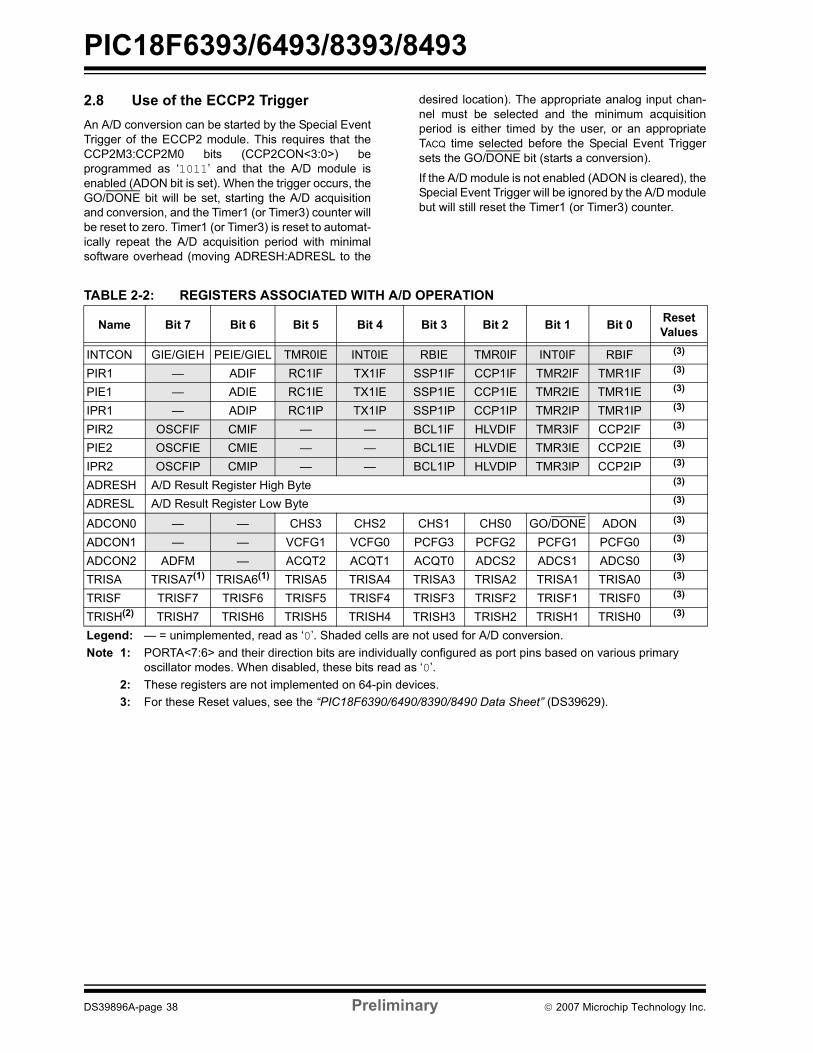
2.8 Use of the ECCP2 TriggerAn A/D conversion can be started by the Special EventTrigger of the ECCP2 module. This requires that theCCP2M3:CCP2M0 bits (CCP2CON<3:0>) beprogrammed as �1011� and that the A/D module isenabled (ADON bit is set). When the trigger occurs, theGO/DONE bit will be set, starting the A/D acquisitionand conversion, and the Timer1 (or Timer3) counter willbe reset to zero. Timer1 (or Timer3) is reset to automat-ically repeat the A/D acquisition period with minimalsoftware overhead (moving ADRESH:ADRESL to the
desired location). The appropriate analog input chan-nel must be selected and the minimum acquisitionperiod is either timed by the user, or an appropriateTACQ time selected before the Special Event Triggersets the GO/DONE bit (starts a conversion).
If the A/D module is not enabled (ADON is cleared), theSpecial Event Trigger will be ignored by the A/D modulebut will still reset the Timer1 (or Timer3) counter.
TABLE 2-2: REGISTERS ASSOCIATED WITH A/D OPERATION
Name Bit 7 Bit 6 Bit 5 Bit 4 Bit 3 Bit 2 Bit 1 Bit 0 Reset Values
INTCON GIE/GIEH PEIE/GIEL TMR0IE INT0IE RBIE TMR0IF INT0IF RBIF (3)
PIR1 � ADIF RC1IF TX1IF SSP1IF CCP1IF TMR2IF TMR1IF (3)
PIE1 � ADIE RC1IE TX1IE SSP1IE CCP1IE TMR2IE TMR1IE (3)
IPR1 � ADIP RC1IP TX1IP SSP1IP CCP1IP TMR2IP TMR1IP (3)
PIR2 OSCFIF CMIF � � BCL1IF HLVDIF TMR3IF CCP2IF (3)
PIE2 OSCFIE CMIE � � BCL1IE HLVDIE TMR3IE CCP2IE (3)
IPR2 OSCFIP CMIP � � BCL1IP HLVDIP TMR3IP CCP2IP (3)
ADRESH A/D Result Register High Byte (3)
ADRESL A/D Result Register Low Byte (3)
ADCON0 � � CHS3 CHS2 CHS1 CHS0 GO/DONE ADON (3)
ADCON1 � � VCFG1 VCFG0 PCFG3 PCFG2 PCFG1 PCFG0 (3)
ADCON2 ADFM � ACQT2 ACQT1 ACQT0 ADCS2 ADCS1 ADCS0 (3)
TRISA TRISA7(1) TRISA6(1) TRISA5 TRISA4 TRISA3 TRISA2 TRISA1 TRISA0 (3)
TRISF TRISF7 TRISF6 TRISF5 TRISF4 TRISF3 TRISF2 TRISF1 TRISF0 (3)
TRISH(2) TRISH7 TRISH6 TRISH5 TRISH4 TRISH3 TRISH2 TRISH1 TRISH0 (3)
Legend: � = unimplemented, read as �0�. Shaded cells are not used for A/D conversion.Note 1: PORTA<7:6> and their direction bits are individually configured as port pins based on various primary
oscillator modes. When disabled, these bits read as �0�.2: These registers are not implemented on 64-pin devices.3: For these Reset values, see the �PIC18F6390/6490/8390/8490 Data Sheet� (DS39629).

© 2007 Microchip Technology Inc. Preliminary DS39896A-page 39
PIC18F6393/6493/8393/8493
3.0 SPECIAL FEATURES OF THE CPU
PIC18F6393/6493/8393/8493 devices include severalfeatures intended to maximize reliability and minimizecost through elimination of external components.These include:� Device ID Registers
3.1 Device ID RegistersThe Device ID registers are �read-only� registers.They identify the device type and revision to deviceprogrammers and can be read by firmware using tablereads.
TABLE 3-1: DEVICE IDs
Note: For additional details on the Configurationbits, refer to Section 23.1 �ConfigurationBits� in the �PIC18F6390/6490/8390/8490Data Sheet� (DS39629). Device ID informa-tion presented in this section is for thePIC18F6393/6493/8393/8493 devices only.
File Name Bit 7 Bit 6 Bit 5 Bit 4 Bit 3 Bit 2 Bit 1 Bit 0Default/
UnprogrammedValue
3FFFFEh DEVID1 DEV2 DEV1 DEV0 REV4 REV3 REV2 REV1 REV0 xxxx xxxx(1)
3FFFFFh DEVID2 DEV10 DEV9 DEV8 DEV7 DEV6 DEV5 DEV4 DEV3 xxxx xxxx(1)
Legend: x = unknownNote 1: See Register 3-1 and Register 3-2 for DEVID values. DEVID registers are read-only and cannot be programmed by the user.

PIC18F6393/6493/8393/8493
DS39896A-page 40 Preliminary © 2007 Microchip Technology Inc.
REGISTER 3-1: DEVID1: DEVICE ID REGISTER 1 FOR PIC18F6393/6493/8393/8493 DEVICES
R R R R R R R RDEV2 DEV1 DEV0 REV4 REV3 REV2 REV1 REV0
bit 7 bit 0
Legend:R = Read-only bit P = Programmable bit U = Unimplemented bit, read as �0�-n = Value when device is unprogrammed u = Unchanged from programmed state
bit 7-5 DEV2:DEV0: Device ID bitsSee Register 3-2 for a complete listing.
bit 4-0 REV4:REV0: Revision ID bitsThese bits are used to indicate the device revision.
REGISTER 3-2: DEVID2: DEVICE ID REGISTER 2 FOR PIC18F6393/6493/8393/8493 DEVICES
R R R R R R R RDEV10 DEV9 DEV8 DEV7 DEV6 DEV5 DEV4 DEV3
bit 7 bit 0
Legend:R = Read-only bit P = Programmable bit U = Unimplemented bit, read as �0�-n = Value when device is unprogrammed u = Unchanged from programmed state
bit 7-0 DEV10:DEV3: Device ID bits
Device DEV10:DEV3(DEVID2<7:0>)
DEV2:DEV0(DEVID1<7:5>)
PIC18F6393 0001 1010 000
PIC18F6493 0000 1110 000
PIC18F8393 0001 1010 001
PIC18F8493 0000 1110 001
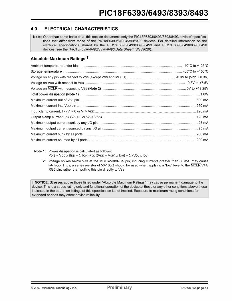
© 2007 Microchip Technology Inc. Preliminary DS39896A-page 41
PIC18F6393/6493/8393/8493
4.0 ELECTRICAL CHARACTERISTICS
Absolute Maximum Ratings(�) Ambient temperature under bias............................................................................................................ .-40°C to +125°C
Storage temperature .............................................................................................................................. -65°C to +150°C
Voltage on any pin with respect to VSS (except VDD and MCLR) ................................................... -0.3V to (VDD + 0.3V)
Voltage on VDD with respect to VSS ......................................................................................................... -0.3V to +7.5V
Voltage on MCLR with respect to VSS (Note 2) ......................................................................................... 0V to +13.25V
Total power dissipation (Note 1) ...............................................................................................................................1.0W
Maximum current out of VSS pin ...........................................................................................................................300 mA
Maximum current into VDD pin ..............................................................................................................................250 mA
Input clamp current, IIK (VI < 0 or VI > VDD)...................................................................................................................... ±20 mA
Output clamp current, IOK (VO < 0 or VO > VDD) .............................................................................................................. ±20 mA
Maximum output current sunk by any I/O pin..........................................................................................................25 mA
Maximum output current sourced by any I/O pin ....................................................................................................25 mA
Maximum current sunk by all ports .......................................................................................................................200 mA
Maximum current sourced by all ports ..................................................................................................................200 mA
Note 1: Power dissipation is calculated as follows: PDIS = VDD x {IDD � ∑ IOH} + ∑ {(VDD � VOH) x IOH} + ∑ (VOL x IOL)
2: Voltage spikes below VSS at the MCLR/VPP/RG5 pin, inducing currents greater than 80 mA, may causelatch-up. Thus, a series resistor of 50-100Ω should be used when applying a �low� level to the MCLR/VPP/RG5 pin, rather than pulling this pin directly to VSS.
Note: Other than some basic data, this section documents only the PIC18F6393/6493/8393/8493 devices� specifica-tions that differ from those of the PIC18F6390/6490/8390/8490 devices. For detailed information on theelectrical specifications shared by the PIC18F6393/6493/8393/8493 and PIC18F6390/6490/8390/8490devices, see the �PIC18F6390/6490/8390/8490 Data Sheet� (DS39629).
� NOTICE: Stresses above those listed under �Absolute Maximum Ratings� may cause permanent damage to the device. This is a stress rating only and functional operation of the device at those or any other conditions above those indicated in the operation listings of this specification is not implied. Exposure to maximum rating conditions for extended periods may affect device reliability.

PIC18F6393/6493/8393/8493
DS39896A-page 42 Preliminary © 2007 Microchip Technology Inc.
FIGURE 4-1: PIC18F6393/6493/8393/8493 VOLTAGE-FREQUENCY GRAPH (INDUSTRIAL)
FIGURE 4-2: PIC18LF6393/6493/8393/8493 VOLTAGE-FREQUENCY GRAPH (INDUSTRIAL)
Frequency
Volta
ge6.0V5.5V
4.5V4.0V
2.0V
40 MHz
5.0V
3.5V
3.0V2.5V
PIC18FX393/X493
4.2V
Frequency
Volta
ge
6.0V5.5V
4.5V4.0V
2.0V
40 MHz
5.0V
3.5V
3.0V2.5V
PIC18LFX393/X493
FMAX = (16.36 MHz/V) (VDDAPPMIN � 2.0V) + 4 MHzNote: VDDAPPMIN is the minimum voltage of the PIC® device in the application.
4 MHz
4.2V

© 2007 Microchip Technology Inc. Preliminary DS39896A-page 43
PIC18F6393/6493/8393/8493TABLE 4-1: A/D CONVERTER CHARACTERISTICS: PIC18F6393/6493/8393/8493 (INDUSTRIAL) Param
No. Sym Characteristic Min Typ Max Units Conditions
A01 NR Resolution � � 12 bit ΔVREF ≥ 3.0V A03 EIL Integral Linearity Error � <±1 ±2.0 LSB VDD = 3.0V
ΔVREF ≥ 3.0V � � ±2.0 LSB VDD = 5.0V
A04 EDL Differential Linearity Error � <±1 +1.5/-1.0 LSB VDD = 3.0VΔVREF ≥ 3.0V
� � +1.5/-1.0 LSB VDD = 5.0VA06 EOFF Offset Error � <±1 ±5 LSB VDD = 3.0V
ΔVREF ≥ 3.0V � � ±3 LSB VDD = 5.0V
A07 EGN Gain Error � <±1 ±2.00 LSB VDD = 3.0VΔVREF ≥ 3.0V
� � ±2.00 LSB VDD = 5.0VA10 � Monotonicity Guaranteed(1) � VSS ≤ VAIN ≤ VREF
A20 ΔVREF Reference Voltage Range(VREFH � VREFL)
3 � VDD � VSS V For 12-bit resolution
A21 VREFH Reference Voltage High VSS + 3.0V � VDD + 0.3V V For 12-bit resolutionA22 VREFL Reference Voltage Low VSS � 0.3V � VDD � 3.0V V For 12-bit resolutionA25 VAIN Analog Input Voltage VREFL � VREFH VA30 ZAIN Recommended
Impedance of Analog Voltage Source
� � 2.5 kΩ
A50 IREF VREF Input Current(2) ��
��
5150
μAμA
During VAIN acquisition.During A/D conversion cycle.
Note 1: The A/D conversion result never decreases with an increase in the input voltage and has no missing codes.2: VREFH current is from the RA3/AN3/VREF+/SEG17 pin or VDD, whichever is selected as the VREFH source. VREFL
current is from the RA2/AN2/VREF-/SEG16 pin or VSS, whichever is selected as the VREFL source.

PIC18F6393/6493/8393/8493
DS39896A-page 44 Preliminary © 2007 Microchip Technology Inc.
FIGURE 4-3: A/D CONVERSION TIMING
TABLE 4-2: A/D CONVERSION REQUIREMENTS
131
130
132
BSF ADCON0, GO
Q4
A/D CLK(1)
A/D DATA
ADRES
ADIF
GO
SAMPLE
OLD_DATA
SAMPLING STOPPED
DONE
NEW_DATA
(Note 2)
11 10 9 3 2 1
Note 1: If the A/D clock source is selected as RC, a time of TCY is added before the A/D clock starts. This allows the SLEEP instructionto be executed.
2: This is a minimal RC delay (typically 100 ns), which also disconnects the holding capacitor from the analog input.
. . . . . .
TCY
0
Param No. Symbol Characteristic Min Max Units Conditions
130 TAD A/D Clock Period PIC18FXXXX 0.8 12.5(1) μs TOSC based, VREF ≥ 3.0VPIC18LFXXXX 1.4 25.0(1) μs VDD = 3.0V; TOSC based,
VREF full rangePIC18FXXXX � 1 μs A/D RC modePIC18LFXXXX � 3 μs VDD = 3.0V; A/D RC mode
131 TCNV Conversion Time (not including acquisition time)(2)
13 14 TAD
132 TACQ Acquisition Time(3) 1.4 � μs135 TSWC Switching Time from Convert → Sample � (Note 4)137 TDIS Discharge Time 0.2 � μsNote 1: The time of the A/D clock period is dependent on the device frequency and the TAD clock divider.
2: ADRES registers may be read on the following TCY cycle.3: The time for the holding capacitor to acquire the �New� input voltage when the voltage changes full scale
after the conversion (VDD to VSS or VSS to VDD). The source impedance (RS) on the input channels is 50Ω.4: On the following cycle of the device clock.

© 2007 Microchip Technology Inc. Preliminary DS39896A-page 45
PIC18F6393/6493/8393/8493
5.0 PACKAGING INFORMATIONFor packaging information, see the �PIC18F6390/6490/8390/8490 Data Sheet� (DS39629).

PIC18F6393/6493/8393/8493
DS39896A-page 46 Preliminary © 2007 Microchip Technology Inc.
NOTES:

© 2007 Microchip Technology Inc. Preliminary DS39896A-page 47
PIC18F6393/6493/8393/8493
APPENDIX A: REVISION HISTORY
Revision A (September 2007)Original data sheet for the PIC18F6393/6493/8393/8493 devices.
APPENDIX B: DEVICE DIFFERENCES
The differences between the devices listed in this datasheet are shown in Table B-1.
TABLE B-1: DEVICE DIFFERENCES Features PIC18F6393 PIC18F6493 PIC18F8393 PIC18F8493
Number of Pixels the LCD Driver Can Drive
128 (4 x 32) 128 (4 x 32) 192 (4 x 48) 192 (4 x 48)
I/O Ports Ports A, B, C, D, E, F, G
Ports A, B, C, D, E, F, G
Ports A, B, C, D, E, F, G, H, J
Ports A, B, C, D, E, F, G, H, J
Flash Program Memory 8 Kbytes 16 Kbytes 8 Kbytes 16 KbytesPackages 64-Pin TQFP 64-Pin TQFP 80-Pin TQFP 80-Pin TQFP

PIC18F6393/6493/8393/8493
DS39896A-page 48 Preliminary © 2007 Microchip Technology Inc.
APPENDIX C: CONVERSION CONSIDERATIONS
This appendix discusses the considerations forconverting from previous versions of a device to theones listed in this data sheet. Typically, these changesare due to the differences in the process technologyused. An example of this type of conversion is from aPIC16C74A to a PIC16C74B.
Not Applicable
APPENDIX D: MIGRATION FROM BASELINE TO ENHANCED DEVICES
This section discusses how to migrate from a Baselinedevice (i.e., PIC16C5X) to an Enhanced MCU device(i.e., PIC18FXXX).
The following are the list of modifications over thePIC16C5X microcontroller family:
Not Currently Available

© 2007 Microchip Technology Inc. Preliminary DS39896A-page 49
PIC18F6393/6493/8393/8493
APPENDIX E: MIGRATION FROM MID-RANGE TO ENHANCED DEVICES
A detailed discussion of the differences between themid-range MCU devices (i.e., PIC16CXXX) and theenhanced devices (i.e., PIC18FXXX) is provided inAN716, �Migrating Designs from PIC16C74A/74B toPIC18C442�. The changes discussed, while device-specific, are generally applicable to all mid-range toenhanced device migrations.
This Application Note is available as Literature NumberDS00716.
APPENDIX F: MIGRATION FROM HIGH-END TO ENHANCED DEVICES
A detailed discussion of the migration pathway anddifferences between the high-end MCU devices (i.e.,PIC17CXXX) and the enhanced devices (i.e.,PIC18FXXX) is provided in AN726, �PIC17CXXX toPIC18CXXX Migration�. This Application Note isavailable as Literature Number DS00726.
PIC18F6393/6493/8393/8493
DS39896A-page 50 Preliminary © 2007 Microchip Technology Inc.
NOTES:

© 2007 Microchip Technology Inc. DS39896A-page 51
PIC18F6393/6493/8393/8493
INDEXAA/D ...................................................................................... 29
A/D Converter Interrupt, Configuring .......................... 33Acquisition Requirements ........................................... 34ADCON0 Register....................................................... 29ADCON1 Register....................................................... 29ADCON2 Register....................................................... 29ADRESH Register................................................. 29, 32ADRESL Register ....................................................... 29Analog Port Pins, Configuring..................................... 36Associated Registers .................................................. 38Configuring the Module............................................... 33Conversion Clock (TAD) .............................................. 35Conversion Requirements .......................................... 44Conversion Status (GO/DONE Bit) ............................. 32Conversions ................................................................ 37Converter Characteristics ........................................... 43Discharge.................................................................... 37Operation in Power-Managed Modes ......................... 36Selecting and Configuring Acquisition Time ............... 35Special Event Trigger (ECCP2) .................................. 38Transfer Function........................................................ 33Use of the ECCP2 Trigger .......................................... 38
Absolute Maximum Ratings ................................................ 41ADCON0 Register............................................................... 29
GO/DONE Bit.............................................................. 32ADCON1 Register............................................................... 29ADCON2 Register............................................................... 29ADRESH Register............................................................... 29ADRESL Register ......................................................... 29, 32Analog-to-Digital Converter. See A/D.
BBlock Diagrams
A/D .............................................................................. 32Analog Input Model ..................................................... 33PIC18F6X93 ................................................................. 9PIC18F8X93 ............................................................... 10
CCompare (ECCP2 Module)
Special Event Trigger.................................................. 38Conversion Considerations ................................................. 48Customer Change Notification Service ............................... 53Customer Notification Service............................................. 53Customer Support ............................................................... 53
DDevice Differences.............................................................. 47Device ID Registers ............................................................ 39Device Overview ................................................................... 7
Details of Individual Devices ......................................... 7Features (table)............................................................. 8Special Features ........................................................... 7
DocumentationMost Current Versions .................................................. 5Related Data Sheet....................................................... 7
EElectrical Characteristics .................................................... 41
A/D Converter............................................................. 43Absolute Maximum Ratings........................................ 41Low-Power Voltage-Frequency Graph ....................... 42Voltage-Frequency Graph .......................................... 42
EquationsA/D Acquisition Time .................................................. 34A/D Minimum Charging Time ..................................... 34Calculating the Minimum Required
Acquisition Time ................................................. 34Errata .................................................................................... 5
IInternet Address ................................................................. 53Interrupt Sources
A/D Conversion Complete .......................................... 33
LLCD Driver
Features ....................................................................... 1
MMicrochip Internet Web Site................................................ 53Microcontroller
Special Features........................................................... 1Migration from Baseline to Enhanced Devices ................... 48Migration from High-End to Enhanced Devices.................. 49Migration from Mid-Range to Enhanced Devices ............... 49
OOscillator Structure
Features ....................................................................... 1
PPackaging
Information.................................................................. 45Peripheral Highlights............................................................. 1Pin Diagrams
64-Pin TQFP................................................................. 280-Pin TQFP................................................................. 3
Pin FunctionsAVDD........................................................................... 28AVDD........................................................................... 18AVSS ........................................................................... 28AVSS ........................................................................... 18COM0 ................................................................... 16, 24LCDBIAS1 ............................................................ 16, 24LCDBIAS2 ............................................................ 16, 24LCDBIAS3 ............................................................ 16, 24MCLR/VPP/RG5.................................................... 11, 19OSC1/CLKI/RA7................................................... 11, 19OSC2/CLKO/RA6 ................................................. 11, 19RA0/AN0............................................................... 12, 20RA1/AN1............................................................... 12, 20RA2/AN2/VREF-/SEG16........................................ 12, 20RA3/AN3/VREF+/SEG17....................................... 12, 20RA4/T0CKI/SEG14............................................... 12, 20

PIC18F6393/6493/8393/8493
DS39896A-page 52 © 2007 Microchip Technology Inc.
RA5/AN4/HLVDIN/SEG15 .................................... 12, 20RB0/INT0 .............................................................. 13, 21RB1/INT1/SEG8.................................................... 13, 21RB2/INT2/SEG9.................................................... 13, 21RB3/INT3/SEG10.................................................. 13, 21RB4/KBI0/SEG11.................................................. 13, 21RB5/KBI1 .............................................................. 13, 21RB6/KBI2/PGC ..................................................... 13, 21RB7/KBI3/PGD ..................................................... 13, 21RC0/T1OSO/T13CKI ............................................ 14, 22RC1/T1OSI/CCP2................................................. 14, 22RC2/CCP1/SEG13................................................ 14, 22RC3/SCK/SCL ...................................................... 14, 22RC4/SDI/SDA ....................................................... 14, 22RC5/SDO/SEG12 ................................................. 14, 22RC6/TX1/CK1 ....................................................... 14, 22RC7/RX1/DT1 ....................................................... 14, 22RD0/SEG0 ............................................................ 15, 23RD0/SEG1 .................................................................. 15RD1/SEG1 .................................................................. 23RD2/SEG2 ............................................................ 15, 23RD3/SEG3 ............................................................ 15, 23RD4/SEG4 ............................................................ 15, 23RD5/SEG5 ............................................................ 15, 23RD6/SEG6 ............................................................ 15, 23RD7/SEG7 ............................................................ 15, 23RE4/COM1............................................................ 16, 24RE5/COM2............................................................ 16, 24RE6/COM3............................................................ 16, 24RE7/CCP2/SEG31................................................ 16, 24RF0/AN5/SEG18................................................... 17, 25RF1/AN6/C2OUT/SEG19 ..................................... 17, 25RF2/AN7/C1OUT/SEG20 ..................................... 17, 25RF3/AN8/SEG21................................................... 17, 25RF4/AN9/SEG22................................................... 17, 25RF5/AN10/CVREF/SEG23..................................... 17, 25RF6/AN11/SEG24................................................. 17, 25RF7/SS/SEG25..................................................... 17, 25RG0/SEG30 .......................................................... 18, 26RG1/TX2/CK2/SEG29 .......................................... 18, 26RG2/RX2/DT2/SEG28 .......................................... 18, 26RG3/SEG27 .......................................................... 18, 26RG4/SEG26 .......................................................... 18, 26RG5....................................................................... 18, 26RH0/SEG47 ................................................................ 27RH1/SEG46 ................................................................ 27RH2/SEG45 ................................................................ 27RH3/SEG44 ................................................................ 27RH4/SEG40 ................................................................ 27RH5/SEG41 ................................................................ 27RH6/SEG42 ................................................................ 27RH7/SEG43 ................................................................ 27RJ0/SEG32 ................................................................. 28RJ1/SEG33 ................................................................. 28RJ2/SEG34 ................................................................. 28RJ3/SEG35 ................................................................. 28RJ4/SEG39 ................................................................. 28RJ5/SEG38 ................................................................. 28RJ6/SEG37 ................................................................. 28RJ7/SEG36 ................................................................. 28VDD.............................................................................. 28VDD.............................................................................. 18VSS.............................................................................. 28VSS.............................................................................. 18
Pinout I/O DescriptionsPIC18F6X93 ............................................................... 11PIC18F8X93 ............................................................... 19
Power-Managed Modesand A/D Operation...................................................... 36Features ....................................................................... 1
Product Identification System ............................................. 55
RReader Response............................................................... 54Registers
ADCON0 (A/D Control 0)............................................ 29ADCON1 (A/D Control 1)............................................ 30ADCON2 (A/D Control 2)............................................ 31DEVID1 (Device ID 1)................................................. 40DEVID2 (Device ID 2)................................................. 40
Revision History.................................................................. 47
SSpecial Features of the CPU .............................................. 39
Device ID Registers .................................................... 39
TTiming Diagrams
A/D Conversion........................................................... 44
WWWW Address ................................................................... 53WWW, On-Line Support ....................................................... 5

© 2007 Microchip Technology Inc. Preliminary DS39896A-page 53
PIC18F6393/6493/8393/8493
THE MICROCHIP WEB SITEMicrochip provides online support via our WWW site atwww.microchip.com. This web site is used as a meansto make files and information easily available tocustomers. Accessible by using your favorite Internetbrowser, the web site contains the followinginformation:
� Product Support � Data sheets and errata, application notes and sample programs, design resources, user�s guides and hardware support documents, latest software releases and archived software
� General Technical Support � Frequently Asked Questions (FAQ), technical support requests, online discussion groups, Microchip consultant program member listing
� Business of Microchip � Product selector and ordering guides, latest Microchip press releases, listing of seminars and events, listings of Microchip sales offices, distributors and factory representatives
CUSTOMER CHANGE NOTIFICATION SERVICEMicrochip�s customer notification service helps keepcustomers current on Microchip products. Subscriberswill receive e-mail notification whenever there arechanges, updates, revisions or errata related to aspecified product family or development tool of interest.
To register, access the Microchip web site atwww.microchip.com, click on Customer ChangeNotification and follow the registration instructions.
CUSTOMER SUPPORTUsers of Microchip products can receive assistancethrough several channels:
� Distributor or Representative� Local Sales Office� Field Application Engineer (FAE)� Technical Support� Development Systems Information Line
Customers should contact their distributor,representative or field application engineer (FAE) forsupport. Local sales offices are also available to helpcustomers. A listing of sales offices and locations isincluded in the back of this document.
Technical support is available through the web siteat: http://support.microchip.com

PIC18F6393/6493/8393/8493
DS39896A-page 54 Preliminary © 2007 Microchip Technology Inc.
READER RESPONSEIt is our intention to provide you with the best documentation possible to ensure successful use of your Microchip prod-uct. If you wish to provide your comments on organization, clarity, subject matter, and ways in which our documentationcan better serve you, please FAX your comments to the Technical Publications Manager at (480) 792-4150.
Please list the following information, and use this outline to provide us with your comments about this document.
To: Technical Publications Manager
RE: Reader ResponseTotal Pages Sent ________
From: Name
CompanyAddressCity / State / ZIP / Country
Telephone: (_______) _________ - _________
Application (optional):
Would you like a reply? Y N
Device: Literature Number:
Questions:
FAX: (______) _________ - _________
DS39896APIC18F6393/6493/8393/8493
1. What are the best features of this document?
2. How does this document meet your hardware and software development needs?
3. Do you find the organization of this document easy to follow? If not, why?
4. What additions to the document do you think would enhance the structure and subject?
5. What deletions from the document could be made without affecting the overall usefulness?
6. Is there any incorrect or misleading information (what and where)?
7. How would you improve this document?

© 2007 Microchip Technology Inc. Preliminary DS39896A-page 55
PIC18F6393/6493/8393/8493
PRODUCT IDENTIFICATION SYSTEMTo order or obtain information, e.g., on pricing or delivery, refer to the factory or the listed sales office.
PART NO. X /XX XXX
PatternPackageTemperatureRange
Device
Device(1), (2) PIC18F6393, PIC18F6493, PIC18F8393, PIC18F8493 �
VDD range: 4.2V to 5.5VPIC18LF6393, PIC18LF6493, PIC18LF8393, PIC18LF8493 � VDD range: 2.0V to 5.5V
Temperature Range I = -40°C to +85°C (Industrial)E = -40°C to +125°C (Extended)
Package PT = TQFP (Thin Quad Flatpack)
Pattern QTP, SQTP, Code or Special Requirements (blank otherwise)
Examples:a) PIC18LF6393-I/PT 301 = Industrial temp.,
TQFP package, Extended VDD limits, QTP pattern #301.
b) PIC18LF6393-I/PT = Industrial temp., TQFP package, Extended VDD limits.
c) PIC18F6393-E/PT = Extended temp., TQFP package, normal VDD limits.
Note 1: F = Standard Voltage RangeLF = Wide Voltage Range
2: T = in tape and reel TQFPpackages only.

DS39896A-page 56 Preliminary © 2007 Microchip Technology Inc.
AMERICASCorporate Office2355 West Chandler Blvd.Chandler, AZ 85224-6199Tel: 480-792-7200 Fax: 480-792-7277Technical Support: http://support.microchip.comWeb Address: www.microchip.comAtlantaDuluth, GA Tel: 678-957-9614 Fax: 678-957-1455BostonWestborough, MA Tel: 774-760-0087 Fax: 774-760-0088ChicagoItasca, IL Tel: 630-285-0071 Fax: 630-285-0075DallasAddison, TX Tel: 972-818-7423 Fax: 972-818-2924DetroitFarmington Hills, MI Tel: 248-538-2250Fax: 248-538-2260KokomoKokomo, IN Tel: 765-864-8360Fax: 765-864-8387Los AngelesMission Viejo, CA Tel: 949-462-9523 Fax: 949-462-9608Santa ClaraSanta Clara, CA Tel: 408-961-6444Fax: 408-961-6445TorontoMississauga, Ontario, CanadaTel: 905-673-0699 Fax: 905-673-6509
ASIA/PACIFICAsia Pacific OfficeSuites 3707-14, 37th FloorTower 6, The GatewayHarbour City, KowloonHong KongTel: 852-2401-1200Fax: 852-2401-3431Australia - SydneyTel: 61-2-9868-6733Fax: 61-2-9868-6755China - BeijingTel: 86-10-8528-2100 Fax: 86-10-8528-2104China - ChengduTel: 86-28-8665-5511Fax: 86-28-8665-7889China - FuzhouTel: 86-591-8750-3506 Fax: 86-591-8750-3521China - Hong Kong SARTel: 852-2401-1200 Fax: 852-2401-3431China - NanjingTel: 86-25-8473-2460Fax: 86-25-8473-2470China - QingdaoTel: 86-532-8502-7355Fax: 86-532-8502-7205China - ShanghaiTel: 86-21-5407-5533 Fax: 86-21-5407-5066China - ShenyangTel: 86-24-2334-2829Fax: 86-24-2334-2393China - ShenzhenTel: 86-755-8203-2660 Fax: 86-755-8203-1760China - ShundeTel: 86-757-2839-5507 Fax: 86-757-2839-5571China - WuhanTel: 86-27-5980-5300Fax: 86-27-5980-5118China - XianTel: 86-29-8833-7252Fax: 86-29-8833-7256
ASIA/PACIFICIndia - BangaloreTel: 91-80-4182-8400 Fax: 91-80-4182-8422India - New DelhiTel: 91-11-4160-8631Fax: 91-11-4160-8632India - PuneTel: 91-20-2566-1512Fax: 91-20-2566-1513Japan - YokohamaTel: 81-45-471- 6166 Fax: 81-45-471-6122Korea - DaeguTel: 82-53-744-4301Fax: 82-53-744-4302Korea - SeoulTel: 82-2-554-7200Fax: 82-2-558-5932 or 82-2-558-5934Malaysia - Kuala LumpurTel: 60-3-6201-9857Fax: 60-3-6201-9859Malaysia - PenangTel: 60-4-646-8870Fax: 60-4-646-5086Philippines - ManilaTel: 63-2-634-9065Fax: 63-2-634-9069SingaporeTel: 65-6334-8870Fax: 65-6334-8850Taiwan - Hsin ChuTel: 886-3-572-9526Fax: 886-3-572-6459Taiwan - KaohsiungTel: 886-7-536-4818Fax: 886-7-536-4803Taiwan - TaipeiTel: 886-2-2500-6610 Fax: 886-2-2508-0102Thailand - BangkokTel: 66-2-694-1351Fax: 66-2-694-1350
EUROPEAustria - WelsTel: 43-7242-2244-39Fax: 43-7242-2244-393Denmark - CopenhagenTel: 45-4450-2828 Fax: 45-4485-2829France - ParisTel: 33-1-69-53-63-20 Fax: 33-1-69-30-90-79Germany - MunichTel: 49-89-627-144-0 Fax: 49-89-627-144-44Italy - Milan Tel: 39-0331-742611 Fax: 39-0331-466781Netherlands - DrunenTel: 31-416-690399 Fax: 31-416-690340Spain - MadridTel: 34-91-708-08-90Fax: 34-91-708-08-91UK - WokinghamTel: 44-118-921-5869Fax: 44-118-921-5820
WORLDWIDE SALES AND SERVICE
09/10/07