PIC18F1220/1320 Data Sheet - Microchip...
310
2004 Microchip Technology Inc. DS39605C PIC18F1220/1320 Data Sheet 18/20/28-Pin High-Performance, Enhanced Flash Microcontrollers with 10-bit A/D and nanoWatt Technology
-
Upload
nguyentram -
Category
Documents
-
view
223 -
download
0
Transcript of PIC18F1220/1320 Data Sheet - Microchip...
2004 Microchip Technology Inc. DS39605C
PIC18F1220/1320Data Sheet
18/20/28-Pin High-Performance,Enhanced Flash Microcontrollers
with 10-bit A/D and nanoWatt Technology

Note the following details of the code protection feature on Microchip devices:
• Microchip products meet the specification contained in their particular Microchip Data Sheet.
• Microchip believes that its family of products is one of the most secure families of its kind on the market today, when used in the intended manner and under normal conditions.
• There are dishonest and possibly illegal methods used to breach the code protection feature. All of these methods, to our knowledge, require using the Microchip products in a manner outside the operating specifications contained in Microchip’s Data Sheets. Most likely, the person doing so is engaged in theft of intellectual property.
• Microchip is willing to work with the customer who is concerned about the integrity of their code.
• Neither Microchip nor any other semiconductor manufacturer can guarantee the security of their code. Code protection does not mean that we are guaranteeing the product as “unbreakable.”
Code protection is constantly evolving. We at Microchip are committed to continuously improving the code protection features of ourproducts. Attempts to break Microchip’s code protection feature may be a violation of the Digital Millennium Copyright Act. If such actsallow unauthorized access to your software or other copyrighted work, you may have a right to sue for relief under that Act.
Information contained in this publication regarding deviceapplications and the like is intended through suggestion onlyand may be superseded by updates. It is your responsibility toensure that your application meets with your specifications.No representation or warranty is given and no liability isassumed by Microchip Technology Incorporated with respectto the accuracy or use of such information, or infringement ofpatents or other intellectual property rights arising from suchuse or otherwise. Use of Microchip’s products as criticalcomponents in life support systems is not authorized exceptwith express written approval by Microchip. No licenses areconveyed, implicitly or otherwise, under any intellectualproperty rights.
DS39605C-page ii
Trademarks
The Microchip name and logo, the Microchip logo, Accuron, dsPIC, KEELOQ, microID, MPLAB, PIC, PICmicro, PICSTART, PRO MATE, PowerSmart, rfPIC, and SmartShunt are registered trademarks of Microchip Technology Incorporated in the U.S.A. and other countries.
AmpLab, FilterLab, MXDEV, MXLAB, PICMASTER, SEEVAL, SmartSensor and The Embedded Control Solutions Company are registered trademarks of Microchip Technology Incorporated in the U.S.A.
Analog-for-the-Digital Age, Application Maestro, dsPICDEM, dsPICDEM.net, dsPICworks, ECAN, ECONOMONITOR, FanSense, FlexROM, fuzzyLAB, In-Circuit Serial Programming, ICSP, ICEPIC, Migratable Memory, MPASM, MPLIB, MPLINK, MPSIM, PICkit, PICDEM, PICDEM.net, PICLAB, PICtail, PowerCal, PowerInfo, PowerMate, PowerTool, rfLAB, rfPICDEM, Select Mode, Smart Serial, SmartTel and Total Endurance are trademarks of Microchip Technology Incorporated in the U.S.A. and other countries.
SQTP is a service mark of Microchip Technology Incorporated in the U.S.A.
All other trademarks mentioned herein are property of their respective companies.
© 2004, Microchip Technology Incorporated, Printed in the U.S.A., All Rights Reserved.
Printed on recycled paper.
2004 Microchip Technology Inc.
Microchip received ISO/TS-16949:2002 quality system certification for its worldwide headquarters, design and wafer fabrication facilities in Chandler and Tempe, Arizona and Mountain View, California in October 2003. The Company’s quality system processes and procedures are for its PICmicro® 8-bit MCUs, KEELOQ® code hopping devices, Serial EEPROMs, microperipherals, nonvolatile memory and analog products. In addition, Microchip’s quality system for the design and manufacture of development systems is ISO 9001:2000 certified.

18/20/28-Pin High-Performance, Enhanced Flash MCUs with 10-bit A/D and nanoWatt Technology
PIC18F1220/1320
Low-Power Features:
• Power Managed modes:- Run: CPU on, peripherals on
- Idle: CPU off, peripherals on- Sleep: CPU off, peripherals off
• Power Consumption modes:
- PRI_RUN: 150 µA, 1 MHz, 2V- PRI_IDLE: 37 µA, 1 MHz, 2V- SEC_RUN: 14 µA, 32 kHz, 2V
- SEC_IDLE: 5.8 µA, 32 kHz, 2V- RC_RUN: 110 µA, 1 MHz, 2V- RC_IDLE: 52 µA, 1 MHz, 2V
- Sleep: 0.1 µA, 1 MHz, 2V• Timer1 Oscillator: 1.1 µA, 32 kHz, 2V• Watchdog Timer: 2.1 µA
• Two-Speed Oscillator Start-up
Oscillators:
• Four Crystal modes:- LP, XT, HS: up to 25 MHz- HSPLL: 4-10 MHz (16-40 MHz internal)
• Two External RC modes, up to 4 MHz• Two External Clock modes, up to 40 MHz
• Internal oscillator block:- 8 user-selectable frequencies: 31 kHz, 125 kHz,
250 kHz, 500 kHz, 1 MHz, 2 MHz, 4 MHz, 8 MHz- 125 kHz to 8 MHz calibrated to 1%
- Two modes select one or two I/O pins- OSCTUNE – Allows user to shift frequency
• Secondary oscillator using Timer1 @ 32 kHz
• Fail-Safe Clock Monitor- Allows for safe shutdown if peripheral clock stops
Peripheral Highlights:
• High current sink/source 25 mA/25 mA• Three external interrupts
• Enhanced Capture/Compare/PWM (ECCP) module:- One, two or four PWM outputs- Selectable polarity
- Programmable dead time- Auto-Shutdown and Auto-Restart- Capture is 16-bit, max resolution 6.25 ns (TCY/16)
- Compare is 16-bit, max resolution 100 ns (TCY)• Compatible 10-bit, up to 13-channel Analog-to-
Digital Converter module (A/D) with programmable acquisition time
• Enhanced USART module:- Supports RS-485, RS-232 and LIN 1.2- Auto-Wake-up on Start bit
- Auto-Baud Detect
Special Microcontroller Features:
• 100,000 erase/write cycle Enhanced Flash program memory typical
• 1,000,000 erase/write cycle Data EEPROM memory typical
• Flash/Data EEPROM Retention: > 40 years• Self-programmable under software control• Priority levels for interrupts
• 8 x 8 Single-Cycle Hardware Multiplier• Extended Watchdog Timer (WDT):
- Programmable period from 41 ms to 131s
- 2% stability over VDD and Temperature• Single-supply 5V In-Circuit Serial Programming™
(ICSP™) via two pins• In-Circuit Debug (ICD) via two pins• Wide operating voltage range: 2.0V to 5.5V
Device
Program Memory Data Memory
I/O10-bit
A/D (ch)ECCP(PWM)
EUSARTTimers8/16-bitFlash
(bytes)# Single-Word Instructions
SRAM (bytes)
EEPROM (bytes)
PIC18F1220 4K 2048 256 256 16 7 1 Y 1/3
PIC18F1320 8K 4096 256 256 16 7 1 Y 1/3
2004 Microchip Technology Inc. DS39605C-page 1

PIC18F1220/1320
Pin Diagrams
RB3/CCP1/P1A
RB2/P1B/INT2
OSC1/CLKI/RA7
OSC2/CLKO/RA6
VDD/AVDD
RB7/PGD/T1OSI/
RB6/PGC/T1OSO/
RB5/PGM/KBI1
RB4/AN6/RX/
RA0/AN0
RA1/AN1/LVDIN
RA4/T0CKI
MCLR/VPP/RA5
VSS/AVSS
RA2/AN2/VREF-
RA3/AN3/VREF+
RB0/AN4/INT0
RB1/AN5/TX/
1
2
3
4
5
6
7
8
9
18
17
16
15
14
13
12
11
10
PIC
18F
1X20
18-Pin PDIP, SOIC
RB3/CCP1/P1A
RB2/P1B/INT2
OSC1/CLKI/RA7
OSC2/CLKO/RA6
VDD
RB7/PGD/T1OSI/
RB6/PGC/T1OSO/
RB5/PGM/KBI1
RB4/AN6/RX/
RA0/AN0
RA1/AN1/LVDIN
RA4/T0CKI
MCLR/VPP/RA5
VSS
RA2/AN2/VREF-
RA3/AN3/VREF+
RB0/AN4/INT0
RB1/AN5/TX/
1
2
3
4
5
7
8
9
10
20
19
18
17
16
14
13
12
11
PIC
18F
1X20
AVDDAVSS 6 15
20-Pin SSOP
28-Pin QFN
16
2
RA
0/A
N0
NC
RA
4/T
0CK
I
MCLR/VPP/RA5
NC
AVSS
NC
RA2/AN2/VREF-
RA
3/A
N3/
VR
EF+
RA
1/A
N1/
LVD
IN
OSC1/CLKI/RA7
OSC2/CLKO/RA6
VDD
NC
AVDD
RB7/PGD/T1OSI/P1D/KBI3
RB6/PGC/T1OSO/T13CKI/P1C/KBI2
NC
RB
5/P
GM
/KB
I1
7
PIC18F1X20
1
3
6
5
4
15
21
19
20
17
18
2228 2627 232425
148 109 131211
VSS
NC
NC
RB
2/P
1B/IN
T2
RB
0/A
N4/
INT
0
RB
1/A
N5/
TX
/CK
/INT
1
NC
RB
4/A
N6/
RX
/DT
/KB
I0R
B3/
CC
P1/
P1A
T13CKI/P1C/KBI2
P1D/KBI3
CK/INT1 DT/KBI0
P1D/KBI3
T13CKI/P1C/KBI2
CK/INT1 DT/KBI0
DS39605C-page 2 2004 Microchip Technology Inc.

PIC18F1220/1320
Table of Contents
1.0 Device Overview .......................................................................................................................................................................... 52.0 Oscillator Configurations ............................................................................................................................................................ 113.0 Power Managed Modes ............................................................................................................................................................. 194.0 Reset .......................................................................................................................................................................................... 335.0 Memory Organization ................................................................................................................................................................. 416.0 Flash Program Memory.............................................................................................................................................................. 577.0 Data EEPROM Memory ............................................................................................................................................................. 678.0 8 x 8 Hardware Multiplier............................................................................................................................................................ 719.0 Interrupts .................................................................................................................................................................................... 7310.0 I/O Ports ..................................................................................................................................................................................... 8711.0 Timer0 Module ........................................................................................................................................................................... 9912.0 Timer1 Module ......................................................................................................................................................................... 10313.0 Timer2 Module ......................................................................................................................................................................... 10914.0 Timer3 Module ......................................................................................................................................................................... 11115.0 Enhanced Capture/Compare/PWM (ECCP) Module................................................................................................................ 11516.0 Enhanced Addressable Universal Synchronous Asynchronous Receiver Transmitter (EUSART) .......................................... 13117.0 10-Bit Analog-to-Digital Converter (A/D) Module ..................................................................................................................... 15518.0 Low-Voltage Detect .................................................................................................................................................................. 16519.0 Special Features of the CPU.................................................................................................................................................... 17120.0 Instruction Set Summary .......................................................................................................................................................... 19121.0 Development Support............................................................................................................................................................... 23322.0 Electrical Characteristics .......................................................................................................................................................... 23923.0 DC and AC Characteristics Graphs and Tables....................................................................................................................... 26924.0 Packaging Information.............................................................................................................................................................. 287Appendix A: Revision History............................................................................................................................................................. 293Appendix B: Device Differences ........................................................................................................................................................ 293Appendix C: Conversion Considerations ........................................................................................................................................... 294Appendix D: Migration from Baseline to Enhanced Devices.............................................................................................................. 294Appendix E: Migration from Mid-Range to Enhanced Devices .......................................................................................................... 295Appendix F: Migration from High-End to Enhanced Devices............................................................................................................. 295Index .................................................................................................................................................................................................. 297On-Line Support................................................................................................................................................................................. 305Systems Information and Upgrade Hot Line ...................................................................................................................................... 305Reader Response .............................................................................................................................................................................. 306PIC18F1220/1320 Product Identification System .............................................................................................................................. 307
2004 Microchip Technology Inc. DS39605C-page 3

PIC18F1220/1320
TO OUR VALUED CUSTOMERS
It is our intention to provide our valued customers with the best documentation possible to ensure successful use of your Microchipproducts. To this end, we will continue to improve our publications to better suit your needs. Our publications will be refined andenhanced as new volumes and updates are introduced.
If you have any questions or comments regarding this publication, please contact the Marketing Communications Department viaE-mail at [email protected] or fax the Reader Response Form in the back of this data sheet to (480) 792-4150.We welcome your feedback.
Most Current Data SheetTo obtain the most up-to-date version of this data sheet, please register at our Worldwide Web site at:
http://www.microchip.com
You can determine the version of a data sheet by examining its literature number found on the bottom outside corner of any page.The last character of the literature number is the version number, (e.g., DS30000A is version A of document DS30000).
ErrataAn errata sheet, describing minor operational differences from the data sheet and recommended workarounds, may exist for currentdevices. As device/documentation issues become known to us, we will publish an errata sheet. The errata will specify the revisionof silicon and revision of document to which it applies.
To determine if an errata sheet exists for a particular device, please check with one of the following:
• Microchip’s Worldwide Web site; http://www.microchip.com• Your local Microchip sales office (see last page)• The Microchip Corporate Literature Center; U.S. FAX: (480) 792-7277When contacting a sales office or the literature center, please specify which device, revision of silicon and data sheet (includeliterature number) you are using.
Customer Notification SystemRegister on our web site at www.microchip.com/cn to receive the most current information on all of our products.
DS39605C-page 4 2004 Microchip Technology Inc.
PIC18F1220/1320
1.0 DEVICE OVERVIEW
This document contains device specific information forthe following devices:
This family offers the advantages of all PIC18 microcon-trollers – namely, high computational performance at aneconomical price – with the addition of high enduranceEnhanced Flash program memory. On top of these fea-tures, the PIC18F1220/1320 family introduces designenhancements that make these microcontrollers a logicalchoice for many high-performance, power sensitiveapplications.
1.1 New Core Features
1.1.1 nanoWatt TECHNOLOGY
All of the devices in the PIC18F1220/1320 family incor-porate a range of features that can significantly reducepower consumption during operation. Key items include:
• Alternate Run Modes: By clocking the controllerfrom the Timer1 source or the internal oscillatorblock, power consumption during code executioncan be reduced by as much as 90%.
• Multiple Idle Modes: The controller can also runwith its CPU core disabled, but the peripherals arestill active. In these states, power consumption canbe reduced even further, to as little as 4% of normaloperation requirements.
• On-the-fly Mode Switching: The power managedmodes are invoked by user code during operation,allowing the user to incorporate power-saving ideasinto their application’s software design.
• Lower Consumption in Key Modules: The powerrequirements for both Timer1 and the WatchdogTimer have been reduced by up to 80%, with typicalvalues of 1.1 and 2.1 µA, respectively.
1.1.2 MULTIPLE OSCILLATOR OPTIONS AND FEATURES
All of the devices in the PIC18F1220/1320 family offernine different oscillator options, allowing users a widerange of choices in developing application hardware.These include:
• Four Crystal modes, using crystals or ceramicresonators.
• Two External Clock modes, offering the option ofusing two pins (oscillator input and a divide-by-4clock output), or one pin (oscillator input, with thesecond pin reassigned as general I/O).
• Two External RC Oscillator modes, with the samepin options as the External Clock modes.
• An internal oscillator block, which provides an8 MHz clock (±2% accuracy) and an INTRC source(approximately 31 kHz, stable over temperature andVDD), as well as a range of 6 user-selectable clockfrequencies (from 125 kHz to 4 MHz) for a total of8 clock frequencies.
Besides its availability as a clock source, the internaloscillator block provides a stable reference source thatgives the family additional features for robustoperation:
• Fail-Safe Clock Monitor: This option constantlymonitors the main clock source against a referencesignal provided by the internal oscillator. If a clock fail-ure occurs, the controller is switched to the internaloscillator block, allowing for continued low-speedoperation, or a safe application shutdown.
• Two-Speed Start-up: This option allows the internaloscillator to serve as the clock source from Power-on Reset, or wake-up from Sleep mode, until theprimary clock source is available. This allows forcode execution during what would otherwise be theclock start-up interval and can even allow an appli-cation to perform routine background activities andreturn to Sleep without returning to full poweroperation.
1.2 Other Special Features
• Memory Endurance: The Enhanced Flash cells forboth program memory and data EEPROM are ratedto last for many thousands of erase/write cycles –up to 100,000 for program memory and 1,000,000for EEPROM. Data retention without refresh isconservatively estimated to be greater than40 years.
• Self-programmability: These devices can write totheir own program memory spaces under internalsoftware control. By using a bootloader routinelocated in the protected Boot Block at the top of pro-gram memory, it becomes possible to create anapplication that can update itself in the field.
• Enhanced CCP module: In PWM mode, thismodule provides 1, 2 or 4 modulated outputs forcontrolling half-bridge and full-bridge drivers. Otherfeatures include auto-shutdown, for disabling PWMoutputs on interrupt or other select conditions andauto-restart, to reactivate outputs once the conditionhas cleared.
• Enhanced USART: This serial communicationmodule features automatic wake-up on Start bit andautomatic baud rate detection and supports RS-232,RS-485 and LIN 1.2 protocols, making it ideallysuited for use in Local Interconnect Network (LIN)bus applications.
• 10-bit A/D Converter: This module incorporatesprogrammable acquisition time, allowing for achannel to be selected and a conversion to beinitiated without waiting for a sampling period andthus, reduce code overhead.
• Extended Watchdog Timer (WDT): This enhancedversion incorporates a 16-bit prescaler, allowing atime-out range from 4 ms to over 2 minutes that isstable across operating voltage and temperature.
• PIC18F1220 • PIC18F1320
2004 Microchip Technology Inc. DS39605C-page 5
PIC18F1220/1320
1.3 Details on Individual Family Members
Devices in the PIC18F1220/1320 family are availablein 18-pin, 20-pin and 28-pin packages. A block diagramfor this device family is shown in Figure 1-1.
The devices are differentiated from each other only inthe amount of on-chip Flash program memory(4 Kbytes for the PIC18F1220 device, 8 Kbytes for thePIC18F1320 device). These and other features aresummarized in Table 1-1.
A block diagram of the PIC18F1220/1320 devicearchitecture is provided in Figure 1-1. The pinouts forthis device family are listed in Table 1-2.
TABLE 1-1: DEVICE FEATURES
Features PIC18F1220 PIC18F1320
Operating Frequency DC – 40 MHz DC – 40 MHz
Program Memory (Bytes) 4096 8192
Program Memory (Instructions) 2048 4096
Data Memory (Bytes) 256 256
Data EEPROM Memory (Bytes) 256 256
Interrupt Sources 15 15
I/O Ports Ports A, B Ports A, B
Timers 4 4
Enhanced Capture/Compare/PWM Modules 1 1
Serial Communications Enhanced USART Enhanced USART
10-bit Analog-to-Digital Module 7 input channels 7 input channels
Resets (and Delays)
POR, BOR, RESET Instruction, Stack Full,
Stack Underflow (PWRT, OST), MCLR (optional), WDT
POR, BOR, RESET Instruction, Stack Full,
Stack Underflow (PWRT, OST), MCLR (optional), WDT
Programmable Low-Voltage Detect Yes Yes
Programmable Brown-out Reset Yes Yes
Instruction Set 75 Instructions 75 Instructions
Packages
18-pin SDIP18-pin SOIC20-pin SSOP28-pin QFN
18-pin SDIP18-pin SOIC20-pin SSOP28-pin QFN
DS39605C-page 6 2004 Microchip Technology Inc.
PIC18F1220/1320
FIGURE 1-1: PIC18F1220/1320 BLOCK DIAGRAM
InstructionDecode &
Control
PORTA
PORTB
RA4/T0CKI
MCLR/VPP/RA5(1)
Enhanced
Timer0 Timer1 Timer2
RA3/AN3/VREF+
RA2/AN2/VREF-
RA1/AN1/LVDIN
RA0/AN0Data Latch
Data RAM
Address Latch
Address<12>
12(2)
BSR FSR0FSR1FSR2
4 12 4
PCH PCL
PCLATH
8
31 Level Stack
Program Counter
PRODLPRODH
8 x 8 Multiply
WREG
8
BIT OP88
ALU<8>
8
Address Latch
(8 Kbytes)
Data Latch
20
21
21
16
8
8
8
inc/dec logic
21 8
Data Bus<8>
8
Instruction
12
3
ROM Latch
Timer3
Bank0, F
PCLATU
PCU
OSC2/CLKO/RA6(2)
USART
8
Register
Table Latch
Table Pointer <2>
inc/dec logic
RB0/AN4/INT0
RB4/AN6/RX/DT/KBI0
RB1/AN5/TX/CK/INT1
RB2/P1B/INT2
RB3/CCP1/P1A
RB5/PGM/KBI1
RB6/PGC/T1OSO/
RB7/PGD/T1OSI/
OSC2/CLKI/RA7(2)Decode
Power-upTimer
Power-onReset
WatchdogTimer
VDD, VSS
Brown-outReset
Precision
ReferenceVoltageLow-Voltage
Programming
In-Circuit Debugger
OscillatorStart-up Timer
TimingGeneration
OSC1(2)
OSC2(2)
T1OSI
T1OSO
INTRCOscillator
Fail-SafeClock Monitor
Note 1: RA5 is available only when the MCLR Reset is disabled.
2: OSC1, OSC2, CLKI and CLKO are only available in select oscillator modes and when these pins are not being used as digitalI/O. Refer to Section 2.0 “Oscillator Configurations” for additional information.
8
CCPEnhanced
T13CKI/P1C/KBI2
Program Memory(4 Kbytes)
PIC18F1220
PIC18F1320
A/D Converter
Data EEPROM
P1D/KBI3
MCLR(1)
2004 Microchip Technology Inc. DS39605C-page 7
PIC18F1220/1320
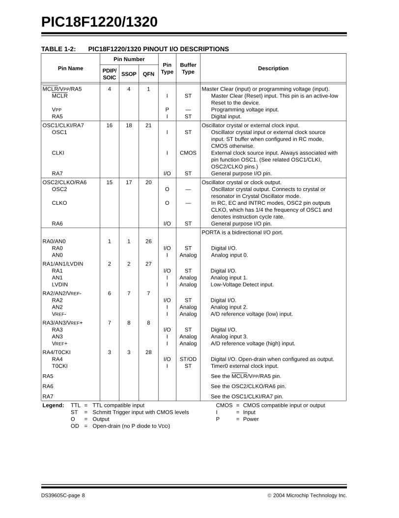
TABLE 1-2: PIC18F1220/1320 PINOUT I/O DESCRIPTIONS
Pin Name
Pin NumberPin
TypeBufferType
DescriptionPDIP/SOIC
SSOP QFN
MCLR/VPP/RA5MCLR
VPP
RA5
4 4 1I
PI
ST
—ST
Master Clear (input) or programming voltage (input).Master Clear (Reset) input. This pin is an active-low Reset to the device.Programming voltage input.Digital input.
OSC1/CLKI/RA7OSC1
CLKI
RA7
16 18 21I
I
I/O
ST
CMOS
ST
Oscillator crystal or external clock input.Oscillator crystal input or external clock source input. ST buffer when configured in RC mode, CMOS otherwise.External clock source input. Always associated with pin function OSC1. (See related OSC1/CLKI, OSC2/CLKO pins.)General purpose I/O pin.
OSC2/CLKO/RA6OSC2
CLKO
RA6
15 17 20O
O
I/O
—
—
ST
Oscillator crystal or clock output.Oscillator crystal output. Connects to crystal or resonator in Crystal Oscillator mode.In RC, EC and INTRC modes, OSC2 pin outputsCLKO, which has 1/4 the frequency of OSC1 and denotes instruction cycle rate.General purpose I/O pin.
PORTA is a bidirectional I/O port.
RA0/AN0RA0AN0
1 1 26I/OI
STAnalog
Digital I/O.Analog input 0.
RA1/AN1/LVDINRA1AN1LVDIN
2 2 27I/OII
STAnalogAnalog
Digital I/O.Analog input 1.Low-Voltage Detect input.
RA2/AN2/VREF-RA2AN2VREF-
6 7 7I/OII
STAnalogAnalog
Digital I/O.Analog input 2.A/D reference voltage (low) input.
RA3/AN3/VREF+RA3AN3VREF+
7 8 8I/OII
STAnalogAnalog
Digital I/O.Analog input 3.A/D reference voltage (high) input.
RA4/T0CKIRA4T0CKI
3 3 28I/OI
ST/ODST
Digital I/O. Open-drain when configured as output.Timer0 external clock input.
RA5 See the MCLR/VPP/RA5 pin.
RA6 See the OSC2/CLKO/RA6 pin.
RA7 See the OSC1/CLKI/RA7 pin.
Legend: TTL = TTL compatible input CMOS = CMOS compatible input or output ST = Schmitt Trigger input with CMOS levels I = Input O = Output P = Power OD = Open-drain (no P diode to VDD)
DS39605C-page 8 2004 Microchip Technology Inc.
PIC18F1220/1320
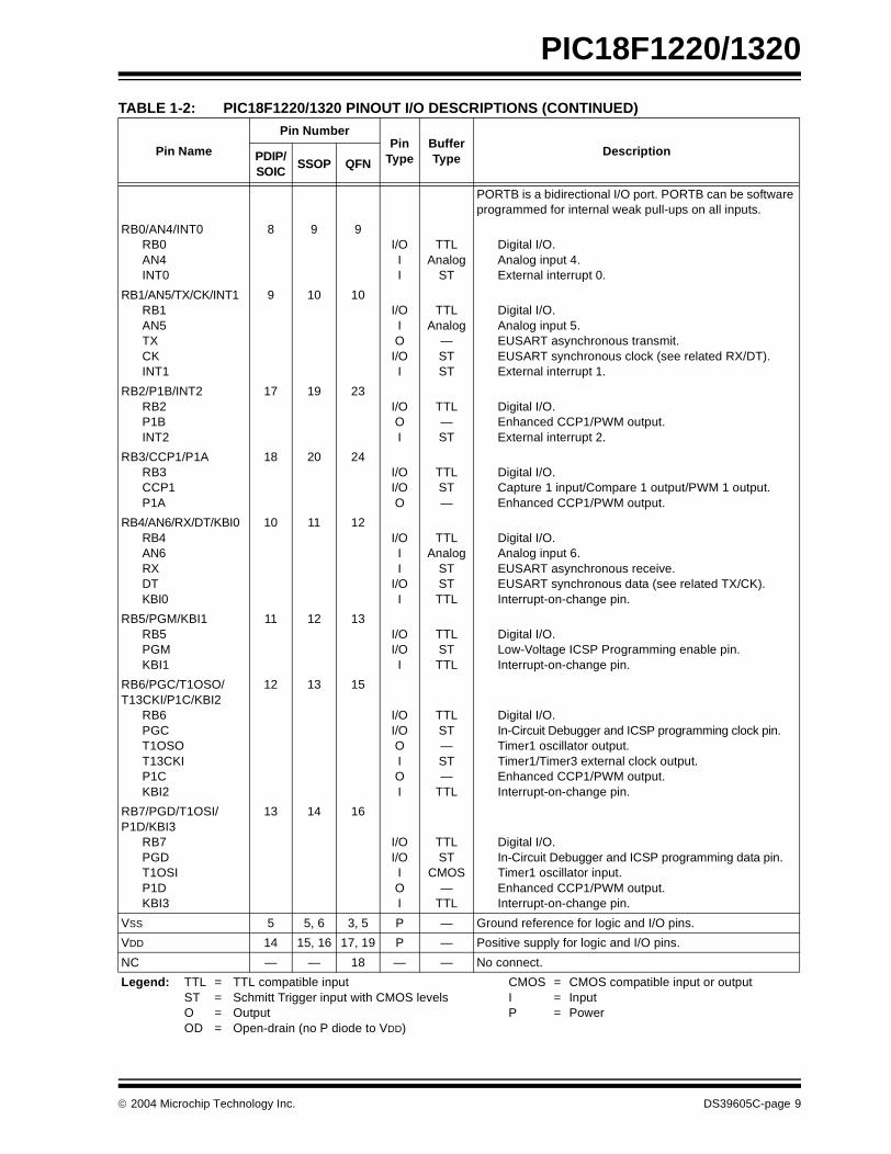
PORTB is a bidirectional I/O port. PORTB can be software programmed for internal weak pull-ups on all inputs.
RB0/AN4/INT0RB0AN4INT0
8 9 9I/OII
TTLAnalog
ST
Digital I/O.Analog input 4.External interrupt 0.
RB1/AN5/TX/CK/INT1RB1AN5TXCKINT1
9 10 10I/OIO
I/OI
TTLAnalog
—STST
Digital I/O.Analog input 5.EUSART asynchronous transmit.EUSART synchronous clock (see related RX/DT).External interrupt 1.
RB2/P1B/INT2RB2P1BINT2
17 19 23I/OOI
TTL—ST
Digital I/O.Enhanced CCP1/PWM output.External interrupt 2.
RB3/CCP1/P1ARB3CCP1P1A
18 20 24I/OI/OO
TTLST—
Digital I/O.Capture 1 input/Compare 1 output/PWM 1 output.Enhanced CCP1/PWM output.
RB4/AN6/RX/DT/KBI0RB4AN6RXDTKBI0
10 11 12I/OII
I/OI
TTLAnalog
STSTTTL
Digital I/O.Analog input 6.EUSART asynchronous receive.EUSART synchronous data (see related TX/CK).Interrupt-on-change pin.
RB5/PGM/KBI1RB5PGMKBI1
11 12 13I/OI/OI
TTLSTTTL
Digital I/O.Low-Voltage ICSP Programming enable pin.Interrupt-on-change pin.
RB6/PGC/T1OSO/T13CKI/P1C/KBI2
RB6PGCT1OSOT13CKIP1CKBI2
12 13 15
I/OI/OOIOI
TTLST—ST—
TTL
Digital I/O.In-Circuit Debugger and ICSP programming clock pin.Timer1 oscillator output.Timer1/Timer3 external clock output.Enhanced CCP1/PWM output.Interrupt-on-change pin.
RB7/PGD/T1OSI/P1D/KBI3
RB7PGDT1OSIP1DKBI3
13 14 16
I/OI/OIOI
TTLST
CMOS—
TTL
Digital I/O.In-Circuit Debugger and ICSP programming data pin.Timer1 oscillator input.Enhanced CCP1/PWM output.Interrupt-on-change pin.
VSS 5 5, 6 3, 5 P — Ground reference for logic and I/O pins.
VDD 14 15, 16 17, 19 P — Positive supply for logic and I/O pins.
NC — — 18 — — No connect.
TABLE 1-2: PIC18F1220/1320 PINOUT I/O DESCRIPTIONS (CONTINUED)
Pin Name
Pin NumberPin
TypeBufferType
DescriptionPDIP/SOIC
SSOP QFN
Legend: TTL = TTL compatible input CMOS = CMOS compatible input or output ST = Schmitt Trigger input with CMOS levels I = Input O = Output P = Power OD = Open-drain (no P diode to VDD)
2004 Microchip Technology Inc. DS39605C-page 9

PIC18F1220/1320
NOTES:
DS39605C-page 10 2004 Microchip Technology Inc.
PIC18F1220/1320
2.0 OSCILLATOR CONFIGURATIONS
2.1 Oscillator Types
The PIC18F1220 and PIC18F1320 devices can beoperated in ten different oscillator modes. The user canprogram the configuration bits, FOSC3:FOSC0, inConfiguration Register 1H to select one of these tenmodes:
1. LP Low-Power Crystal
2. XT Crystal/Resonator3. HS High-Speed Crystal/Resonator4. HSPLL High-Speed Crystal/Resonator
with PLL enabled5. RC External Resistor/Capacitor with
FOSC/4 output on RA66. RCIO External Resistor/Capacitor with
I/O on RA67. INTIO1 Internal Oscillator with FOSC/4
output on RA6 and I/O on RA78. INTIO2 Internal Oscillator with I/O on RA6
and RA79. EC External Clock with FOSC/4 output
10. ECIO External Clock with I/O on RA6
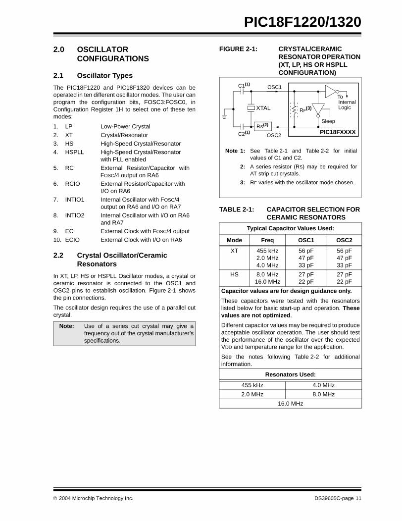
2.2 Crystal Oscillator/Ceramic Resonators
In XT, LP, HS or HSPLL Oscillator modes, a crystal orceramic resonator is connected to the OSC1 andOSC2 pins to establish oscillation. Figure 2-1 showsthe pin connections.
The oscillator design requires the use of a parallel cutcrystal.
FIGURE 2-1: CRYSTAL/CERAMIC RESONATOR OPERATION (XT, LP, HS OR HSPLL CONFIGURATION)
TABLE 2-1: CAPACITOR SELECTION FOR CERAMIC RESONATORS
Note: Use of a series cut crystal may give afrequency out of the crystal manufacturer’sspecifications.
Typical Capacitor Values Used:
Mode Freq OSC1 OSC2
XT 455 kHz2.0 MHz4.0 MHz
56 pF47 pF33 pF
56 pF47 pF33 pF
HS 8.0 MHz16.0 MHz
27 pF22 pF
27 pF22 pF
Capacitor values are for design guidance only.
These capacitors were tested with the resonatorslisted below for basic start-up and operation. Thesevalues are not optimized.
Different capacitor values may be required to produceacceptable oscillator operation. The user should testthe performance of the oscillator over the expectedVDD and temperature range for the application.
See the notes following Table 2-2 for additionalinformation.
Resonators Used:
455 kHz 4.0 MHz
2.0 MHz 8.0 MHz
16.0 MHz
Note 1: See Table 2-1 and Table 2-2 for initialvalues of C1 and C2.
2: A series resistor (RS) may be required forAT strip cut crystals.
3: RF varies with the oscillator mode chosen.
C1(1)
C2(1)
XTAL
OSC2
OSC1
RF(3)
Sleep
To
Logic
PIC18FXXXXRS(2)
Internal
2004 Microchip Technology Inc. DS39605C-page 11
PIC18F1220/1320
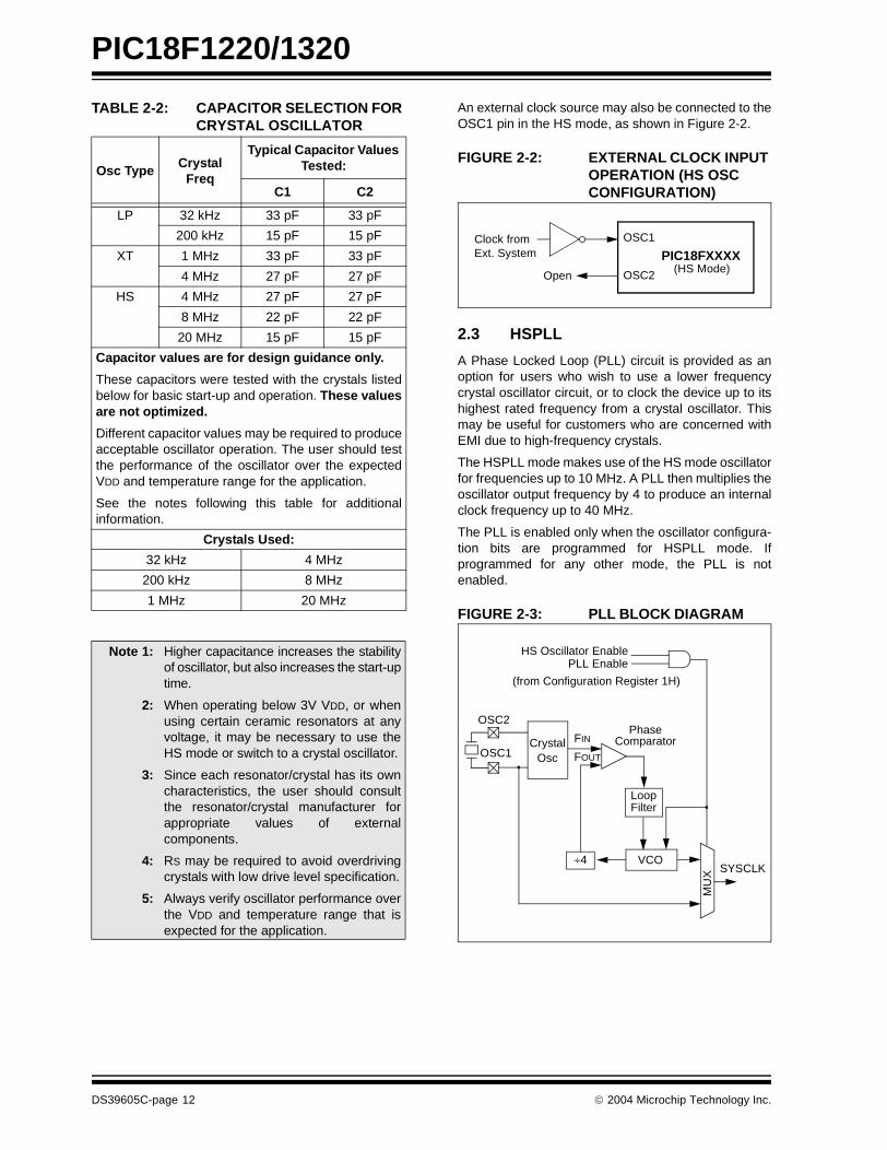
TABLE 2-2: CAPACITOR SELECTION FOR CRYSTAL OSCILLATOR
An external clock source may also be connected to theOSC1 pin in the HS mode, as shown in Figure 2-2.
FIGURE 2-2: EXTERNAL CLOCK INPUT OPERATION (HS OSC CONFIGURATION)
2.3 HSPLL
A Phase Locked Loop (PLL) circuit is provided as anoption for users who wish to use a lower frequencycrystal oscillator circuit, or to clock the device up to itshighest rated frequency from a crystal oscillator. Thismay be useful for customers who are concerned withEMI due to high-frequency crystals.
The HSPLL mode makes use of the HS mode oscillatorfor frequencies up to 10 MHz. A PLL then multiplies theoscillator output frequency by 4 to produce an internalclock frequency up to 40 MHz.
The PLL is enabled only when the oscillator configura-tion bits are programmed for HSPLL mode. Ifprogrammed for any other mode, the PLL is notenabled.
FIGURE 2-3: PLL BLOCK DIAGRAM
Osc TypeCrystal
Freq
Typical Capacitor Values Tested:
C1 C2
LP 32 kHz 33 pF 33 pF
200 kHz 15 pF 15 pF
XT 1 MHz 33 pF 33 pF
4 MHz 27 pF 27 pF
HS 4 MHz 27 pF 27 pF
8 MHz 22 pF 22 pF
20 MHz 15 pF 15 pF
Capacitor values are for design guidance only.
These capacitors were tested with the crystals listedbelow for basic start-up and operation. These valuesare not optimized.
Different capacitor values may be required to produceacceptable oscillator operation. The user should testthe performance of the oscillator over the expectedVDD and temperature range for the application.
See the notes following this table for additionalinformation.
Crystals Used:
32 kHz 4 MHz
200 kHz 8 MHz
1 MHz 20 MHz
Note 1: Higher capacitance increases the stabilityof oscillator, but also increases the start-uptime.
2: When operating below 3V VDD, or whenusing certain ceramic resonators at anyvoltage, it may be necessary to use theHS mode or switch to a crystal oscillator.
3: Since each resonator/crystal has its owncharacteristics, the user should consultthe resonator/crystal manufacturer forappropriate values of externalcomponents.
4: RS may be required to avoid overdrivingcrystals with low drive level specification.
5: Always verify oscillator performance overthe VDD and temperature range that isexpected for the application.
OSC1
OSC2Open
Clock fromExt. System PIC18FXXXX
(HS Mode)
MU
X
VCO
LoopFilter
CrystalOsc
OSC2
OSC1
PLL Enable
FIN
FOUT
SYSCLK
PhaseComparator
HS Oscillator Enable
÷4
(from Configuration Register 1H)
DS39605C-page 12 2004 Microchip Technology Inc.
PIC18F1220/1320
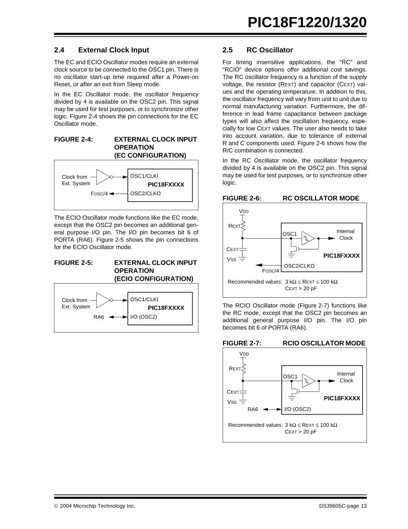
2.4 External Clock Input
The EC and ECIO Oscillator modes require an externalclock source to be connected to the OSC1 pin. There isno oscillator start-up time required after a Power-onReset, or after an exit from Sleep mode.
In the EC Oscillator mode, the oscillator frequencydivided by 4 is available on the OSC2 pin. This signalmay be used for test purposes, or to synchronize otherlogic. Figure 2-4 shows the pin connections for the ECOscillator mode.
FIGURE 2-4: EXTERNAL CLOCK INPUT OPERATION (EC CONFIGURATION)
The ECIO Oscillator mode functions like the EC mode,except that the OSC2 pin becomes an additional gen-eral purpose I/O pin. The I/O pin becomes bit 6 ofPORTA (RA6). Figure 2-5 shows the pin connectionsfor the ECIO Oscillator mode.
FIGURE 2-5: EXTERNAL CLOCK INPUT OPERATION (ECIO CONFIGURATION)
2.5 RC Oscillator
For timing insensitive applications, the “RC” and“RCIO” device options offer additional cost savings.The RC oscillator frequency is a function of the supplyvoltage, the resistor (REXT) and capacitor (CEXT) val-ues and the operating temperature. In addition to this,the oscillator frequency will vary from unit to unit due tonormal manufacturing variation. Furthermore, the dif-ference in lead frame capacitance between packagetypes will also affect the oscillation frequency, espe-cially for low CEXT values. The user also needs to takeinto account variation, due to tolerance of externalR and C components used. Figure 2-6 shows how theR/C combination is connected.
In the RC Oscillator mode, the oscillator frequencydivided by 4 is available on the OSC2 pin. This signalmay be used for test purposes, or to synchronize otherlogic.
FIGURE 2-6: RC OSCILLATOR MODE
The RCIO Oscillator mode (Figure 2-7) functions likethe RC mode, except that the OSC2 pin becomes anadditional general purpose I/O pin. The I/O pinbecomes bit 6 of PORTA (RA6).
FIGURE 2-7: RCIO OSCILLATOR MODE
OSC1/CLKI
OSC2/CLKOFOSC/4
Clock fromExt. System PIC18FXXXX
OSC1/CLKI
I/O (OSC2)RA6
Clock fromExt. System PIC18FXXXX
OSC2/CLKO
CEXT
REXT
PIC18FXXXX
OSC1
FOSC/4
InternalClock
VDD
VSS
Recommended values: 3 kΩ ≤ REXT ≤ 100 kΩCEXT > 20 pF
CEXT
REXT
PIC18FXXXX
OSC1 InternalClock
VDD
VSS
Recommended values: 3 kΩ ≤ REXT ≤ 100 kΩCEXT > 20 pF
I/O (OSC2)RA6
2004 Microchip Technology Inc. DS39605C-page 13

PIC18F1220/1320
2.6 Internal Oscillator Block
The PIC18F1220/1320 devices include an internaloscillator block, which generates two different clocksignals; either can be used as the system’s clocksource. This can eliminate the need for externaloscillator circuits on the OSC1 and/or OSC2 pins.
The main output (INTOSC) is an 8 MHz clock source,which can be used to directly drive the system clock. Italso drives a postscaler, which can provide a range ofclock frequencies from 125 kHz to 4 MHz. TheINTOSC output is enabled when a system clockfrequency from 125 kHz to 8 MHz is selected.
The other clock source is the internal RC oscillator(INTRC), which provides a 31 kHz output. The INTRCoscillator is enabled by selecting the internal oscillatorblock as the system clock source, or when any of thefollowing are enabled:
• Power-up Timer • Fail-Safe Clock Monitor
• Watchdog Timer• Two-Speed Start-up
These features are discussed in greater detail inSection 19.0 “Special Features of the CPU”.
The clock source frequency (INTOSC direct, INTRCdirect or INTOSC postscaler) is selected by configuringthe IRCF bits of the OSCCON register (Register 2-2).
2.6.1 INTIO MODES
Using the internal oscillator as the clock source caneliminate the need for up to two external oscillator pins,which can then be used for digital I/O. Two distinctconfigurations are available:
• In INTIO1 mode, the OSC2 pin outputs FOSC/4, while OSC1 functions as RA7 for digital input and output.
• In INTIO2 mode, OSC1 functions as RA7 and OSC2 functions as RA6, both for digital input and output.
2.6.2 INTRC OUTPUT FREQUENCY
The internal oscillator block is calibrated at the factoryto produce an INTOSC output frequency of 8.0 MHz(see Table 22-6). This changes the frequency of theINTRC source from its nominal 31.25 kHz. Peripheralsand features that depend on the INTRC source will beaffected by this shift in frequency.
Once set during factory calibration, the INTRCfrequency will remain within ±2% as temperature andVDD change across their full specified operatingranges.
2.6.3 OSCTUNE REGISTER
The internal oscillator’s output has been calibrated atthe factory, but can be adjusted in the user’s applica-tion. This is done by writing to the OSCTUNE register(Register 2-1). The tuning sensitivity is constantthroughout the tuning range.
When the OSCTUNE register is modified, the INTOSCand INTRC frequencies will begin shifting to the newfrequency. The INTRC clock will reach the newfrequency within 8 clock cycles (approximately8 * 32 µs = 256 µs). The INTOSC clock will stabilizewithin 1 ms. Code execution continues during this shift.There is no indication that the shift has occurred.Operation of features that depend on the INTRC clocksource frequency, such as the WDT, Fail-Safe ClockMonitor and peripherals, will also be affected by thechange in frequency.
DS39605C-page 14 2004 Microchip Technology Inc.

PIC18F1220/1320
REGISTER 2-1: OSCTUNE: OSCILLATOR TUNING REGISTER
2.7 Clock Sources and Oscillator Switching
Like previous PIC18 devices, the PIC18F1220/1320devices include a feature that allows the system clocksource to be switched from the main oscillator to analternate low-frequency clock source. PIC18F1220/1320 devices offer two alternate clock sources. Whenenabled, these give additional options for switching tothe various power managed operating modes.
Essentially, there are three clock sources for thesedevices:
• Primary oscillators• Secondary oscillators• Internal oscillator block
The primary oscillators include the External Crystaland Resonator modes, the External RC modes, theExternal Clock modes and the internal oscillator block.The particular mode is defined on POR by the contentsof Configuration Register 1H. The details of thesemodes are covered earlier in this chapter.
The secondary oscillators are those external sourcesnot connected to the OSC1 or OSC2 pins. Thesesources may continue to operate even after thecontroller is placed in a power managed mode.
PIC18F1220/1320 devices offer only the Timer1oscillator as a secondary oscillator. This oscillator, in allpower managed modes, is often the time base forfunctions such as a real-time clock.
Most often, a 32.768 kHz watch crystal is connectedbetween the RB6/T1OSO and RB7/T1OSI pins. Likethe LP mode oscillator circuit, loading capacitors arealso connected from each pin to ground. These pinsare also used during ICSP operations.
The Timer1 oscillator is discussed in greater detail inSection 12.2 “Timer1 Oscillator”.
In addition to being a primary clock source, the internaloscillator block is available as a power managedmode clock source. The INTRC source is also used asthe clock source for several special features, such asthe WDT and Fail-Safe Clock Monitor.
The clock sources for the PIC18F1220/1320 devicesare shown in Figure 2-8. See Section 12.0 “Timer1Module” for further details of the Timer1 oscillator. SeeSection 19.1 “Configuration Bits” for configurationregister details.
U-0 U-0 R/W-0 R/W-0 R/W-0 R/W-0 R/W-0 R/W-0
— — TUN5 TUN4 TUN3 TUN2 TUN1 TUN0
bit 7 bit 0
bit 7-6 Unimplemented: Read as ‘0’
bit 5-0 TUN<5:0>: Frequency Tuning bits011111 = Maximum frequency• •• •000001 000000 = Center frequency. Oscillator module is running at the calibrated frequency.111111 • •• •100000 = Minimum frequency
Legend:R = Readable bit W = Writable bit U = Unimplemented bit, read as ‘0’-n = Value at POR ‘1’ = Bit is set ‘0’ = Bit is cleared x = Bit is unknown
2004 Microchip Technology Inc. DS39605C-page 15

PIC18F1220/1320
2.7.1 OSCILLATOR CONTROL REGISTER
The OSCCON register (Register 2-2) controls severalaspects of the system clock’s operation, both in fullpower operation and in power managed modes.
The System Clock Select bits, SCS1:SCS0, select theclock source that is used when the device is operating inpower managed modes. The available clock sources arethe primary clock (defined in Configuration Register 1H),the secondary clock (Timer1 oscillator) and the internaloscillator block. The clock selection has no effect until aSLEEP instruction is executed and the device enters apower managed mode of operation. The SCS bits arecleared on all forms of Reset.
The Internal Oscillator Select bits, IRCF2:IRCF0, selectthe frequency output of the internal oscillator block thatis used to drive the system clock. The choices are theINTRC source, the INTOSC source (8 MHz), or one ofthe six frequencies derived from the INTOSCpostscaler (125 kHz to 4 MHz). If the internal oscillatorblock is supplying the system clock, changing thestates of these bits will have an immediate change onthe internal oscillator’s output.
The OSTS, IOFS and T1RUN bits indicate which clocksource is currently providing the system clock. TheOSTS indicates that the Oscillator Start-up Timer hastimed out and the primary clock is providing the systemclock in Primary Clock modes. The IOFS bit indicates
when the internal oscillator block has stabilized and isproviding the system clock in RC Clock modes orduring Two-Speed Start-ups. The T1RUN bit(T1CON<6>) indicates when the Timer1 oscillator isproviding the system clock in Secondary Clock modes.In power managed modes, only one of these three bitswill be set at any time. If none of these bits are set, theINTRC is providing the system clock, or the internaloscillator block has just started and is not yet stable.
The IDLEN bit controls the selective shutdown of thecontroller’s CPU in power managed modes. The usesof these bits are discussed in more detail inSection 3.0 “Power Managed Modes”.
FIGURE 2-8: PIC18F1220/1320 CLOCK DIAGRAM
Note 1: The Timer1 oscillator must be enabled toselect the secondary clock source. TheTimer1 oscillator is enabled by setting theT1OSCEN bit in the Timer1 Control regis-ter (T1CON<3>). If the Timer1 oscillatoris not enabled, then any attempt to selecta secondary clock source whenexecuting a SLEEP instruction will beignored.
2: It is recommended that the Timer1 oscil-lator be operating and stable before exe-cuting the SLEEP instruction or a verylong delay may occur while the Timer1oscillator starts.
PIC18F1220/1320
4 x PLL
CONFIG1H <3:0>
Secondary Oscillator
T1OSCENEnableOscillator
T1OSO
T1OSI
Clock Source Option for Other Modules
OSC1
OSC2
Sleep
Primary Oscillator
HSPLL
LP, XT, HS, RC, EC
T1OSC
CPU
Peripherals
IDLEN
Pos
tsca
ler
MU
X
MU
X
8
4 MHz
2 MHz
1 MHz
500 kHz
125 kHz
250 kHz
OSCCON<6:4>
111
110
101
100
011
010
001
00031 kHz
INTRCSource
InternalOscillator
Block
WDT, FSCM
8 MHz
Internal Oscillator
(INTOSC)
OSCCON<6:4>
ClockControl OSCCON<1:0>
DS39605C-page 16 2004 Microchip Technology Inc.

PIC18F1220/1320
REGISTER 2-2: OSCCON REGISTER R/W-0 R/W-0 R/W-0 R/W-0 R(1) R-0 R/W-0 R/W-0
IDLEN IRCF2 IRCF1 IRCF0 OSTS IOFS SCS1 SCS0
bit 7 bit 0
bit 7 IDLEN: Idle Enable bits1 = Idle mode enabled; CPU core is not clocked in power managed modes0 = Run mode enabled; CPU core is clocked in Run modes, but not Sleep mode
bit 6-4 IRCF2:IRCF0: Internal Oscillator Frequency Select bits
111 = 8 MHz (8 MHz source drives clock directly)110 = 4 MHz 101 = 2 MHz 100 = 1 MHz 011 = 500 kHz 010 = 250 kHz001 = 125 kHz000 = 31 kHz (INTRC source drives clock directly)
bit 3 OSTS: Oscillator Start-up Time-out Status bit1 = Oscillator Start-up Timer time-out has expired; primary oscillator is running0 = Oscillator Start-up Timer time-out is running; primary oscillator is not ready
bit 2 IOFS: INTOSC Frequency Stable bit 1 = INTOSC frequency is stable0 = INTOSC frequency is not stable
bit 1-0 SCS1:SCS0: System Clock Select bits
1x = Internal oscillator block (RC modes)01 = Timer1 oscillator (Secondary modes)00 = Primary oscillator (Sleep and PRI_IDLE modes)
Note 1: Depends on state of the IESO bit in Configuration Register 1H.
Legend:
R = Readable bit W = Writable bit U = Unimplemented bit, read as ‘0’
-n = Value at POR ‘1’ = Bit is set ‘0’ = Bit is cleared x = Bit is unknown
2004 Microchip Technology Inc. DS39605C-page 17

PIC18F1220/1320
2.7.2 OSCILLATOR TRANSITIONS
The PIC18F1220/1320 devices contain circuitry toprevent clocking “glitches” when switching betweenclock sources. A short pause in the system clockoccurs during the clock switch. The length of this pauseis between 8 and 9 clock periods of the new clocksource. This ensures that the new clock source isstable and that its pulse width will not be less than theshortest pulse width of the two clock sources.
Clock transitions are discussed in greater detail inSection 3.1.2 “Entering Power Managed Modes”.
2.8 Effects of Power Managed Modes on the Various Clock Sources
When the device executes a SLEEP instruction, thesystem is switched to one of the power managedmodes, depending on the state of the IDLEN andSCS1:SCS0 bits of the OSCCON register. SeeSection 3.0 “Power Managed Modes” for details.
When PRI_IDLE mode is selected, the designated pri-mary oscillator continues to run without interruption.For all other power managed modes, the oscillatorusing the OSC1 pin is disabled. The OSC1 pin (andOSC2 pin, if used by the oscillator) will stop oscillating.
In Secondary Clock modes (SEC_RUN andSEC_IDLE), the Timer1 oscillator is operating andproviding the system clock. The Timer1 oscillator mayalso run in all power managed modes if required toclock Timer1 or Timer3.
In Internal Oscillator modes (RC_RUN and RC_IDLE),the internal oscillator block provides the system clocksource. The INTRC output can be used directly toprovide the system clock and may be enabled tosupport various special features, regardless of thepower managed mode (see Section 19.2 “WatchdogTimer (WDT)” through Section 19.4 “Fail-Safe ClockMonitor”). The INTOSC output at 8 MHz may be useddirectly to clock the system, or may be divided downfirst. The INTOSC output is disabled if the system clockis provided directly from the INTRC output.
If the Sleep mode is selected, all clock sources arestopped. Since all the transistor switching currentshave been stopped, Sleep mode achieves the lowestcurrent consumption of the device (only leakagecurrents).
Enabling any on-chip feature that will operate duringSleep will increase the current consumed during Sleep.The INTRC is required to support WDT operation. TheTimer1 oscillator may be operating to support a real-time clock. Other features may be operating that do notrequire a system clock source (i.e., INTn pins, A/Dconversions and others).
2.9 Power-up Delays
Power-up delays are controlled by two timers, so thatno external Reset circuitry is required for most applica-tions. The delays ensure that the device is kept inReset until the device power supply is stable under nor-mal circumstances and the primary clock is operatingand stable. For additional information on power-updelays, see Sections 4.1 through 4.5.
The first timer is the Power-up Timer (PWRT), whichprovides a fixed delay on power-up (parameter 33,Table 22-8) if enabled in Configuration Register 2L.The second timer is the Oscillator Start-up Timer(OST), intended to keep the chip in Reset until thecrystal oscillator is stable (LP, XT and HS modes). TheOST does this by counting 1024 oscillator cyclesbefore allowing the oscillator to clock the device.
When the HSPLL Oscillator mode is selected, thedevice is kept in Reset for an additional 2 ms followingthe HS mode OST delay, so the PLL can lock to theincoming clock frequency.
There is a delay of 5 to 10 µs following POR while thecontroller becomes ready to execute instructions. Thisdelay runs concurrently with any other delays. Thismay be the only delay that occurs when any of the EC,RC or INTIO modes are used as the primary clocksource.
TABLE 2-3: OSC1 AND OSC2 PIN STATES IN SLEEP MODE
Oscillator Mode OSC1 Pin OSC2 Pin
RC, INTIO1 Floating, external resistor should pull high At logic low (clock/4 output)
RCIO, INTIO2 Floating, external resistor should pull high Configured as PORTA, bit 6
ECIO Floating, pulled by external clock Configured as PORTA, bit 6
EC Floating, pulled by external clock At logic low (clock/4 output)
LP, XT and HS Feedback inverter disabled at quiescent voltage level
Feedback inverter disabled at quiescent voltage level
Note: See Table 4-1 in Section 4.0 “Reset” for time-outs due to Sleep and MCLR Reset.
DS39605C-page 18 2004 Microchip Technology Inc.

PIC18F1220/1320
3.0 POWER MANAGED MODES
The PIC18F1220/1320 devices offer a total of six oper-ating modes for more efficient power management(see Table 3-1). These provide a variety of options forselective power conservation in applications whereresources may be limited (i.e., battery powereddevices).
There are three categories of power managed modes:
• Sleep mode • Idle modes
• Run modes
These categories define which portions of the deviceare clocked and sometimes, what speed. The Run andIdle modes may use any of the three available clocksources (primary, secondary or INTOSC multiplexer);the Sleep mode does not use a clock source.
The clock switching feature offered in other PIC18devices (i.e., using the Timer1 oscillator in place of theprimary oscillator) and the Sleep mode offered by allPICmicro® devices (where all system clocks arestopped) are both offered in the PIC18F1220/1320devices (SEC_RUN and Sleep modes, respectively).However, additional power managed modes are avail-able that allow the user greater flexibility in determiningwhat portions of the device are operating. The powermanaged modes are event driven; that is, somespecific event must occur for the device to enter or(more particularly) exit these operating modes.
For PIC18F1220/1320 devices, the power managedmodes are invoked by using the existing SLEEPinstruction. All modes exit to PRI_RUN mode when trig-gered by an interrupt, a Reset or a WDT time-out(PRI_RUN mode is the normal full power executionmode; the CPU and peripherals are clocked by the pri-mary oscillator source). In addition, power managedRun modes may also exit to Sleep mode, or theircorresponding Idle mode.
3.1 Selecting Power Managed Modes
Selecting a power managed mode requires deciding ifthe CPU is to be clocked or not and selecting a clocksource. The IDLEN bit controls CPU clocking, while theSCS1:SCS0 bits select a clock source. The individualmodes, bit settings, clock sources and affectedmodules are summarized in Table 3-1.
3.1.1 CLOCK SOURCES
The clock source is selected by setting the SCS bits ofthe OSCCON register (Register 2-2). Three clocksources are available for use in power managed Idlemodes: the primary clock (as configured in ConfigurationRegister 1H), the secondary clock (Timer1 oscillator)and the internal oscillator block. The secondary andinternal oscillator block sources are available for thepower managed modes (PRI_RUN mode is the normalfull power execution mode; the CPU and peripherals areclocked by the primary oscillator source).
TABLE 3-1: POWER MANAGED MODES
Mode
OSCCON Bits Module Clocking
Available Clock and Oscillator SourceIDLEN<7>
SCS1:SCS0<1:0>
CPU Peripherals
Sleep 0 00 Off Off None – All clocks are disabled
PRI_RUN 0 00 Clocked Clocked Primary – LP, XT, HS, HSPLL, RC, EC, INTRC(1)
This is the normal full power execution mode.
SEC_RUN 0 01 Clocked Clocked Secondary – Timer1 Oscillator
RC_RUN 0 1x Clocked Clocked Internal Oscillator Block(1)
PRI_IDLE 1 00 Off Clocked Primary – LP, XT, HS, HSPLL, RC, EC
SEC_IDLE 1 01 Off Clocked Secondary – Timer1 Oscillator
RC_IDLE 1 1x Off Clocked Internal Oscillator Block(1)
Note 1: Includes INTOSC and INTOSC postscaler, as well as the INTRC source.
2004 Microchip Technology Inc. DS39605C-page 19
PIC18F1220/1320
3.1.2 ENTERING POWER MANAGED MODES
In general, entry, exit and switching between powermanaged clock sources requires clock sourceswitching. In each case, the sequence of events is thesame.
Any change in the power managed mode begins withloading the OSCCON register and executing a SLEEPinstruction. The SCS1:SCS0 bits select one of threepower managed clock sources; the primary clock (asdefined in Configuration Register 1H), the secondaryclock (the Timer1 oscillator) and the internal oscillatorblock (used in RC modes). Modifying the SCS bits willhave no effect until a SLEEP instruction is executed.Entry to the power managed mode is triggered by theexecution of a SLEEP instruction.
Figure 3-5 shows how the system is clocked whileswitching from the primary clock to the Timer1 oscilla-tor. When the SLEEP instruction is executed, clocks tothe device are stopped at the beginning of the nextinstruction cycle. Eight clock cycles from the new clocksource are counted to synchronize with the new clocksource. After eight clock pulses from the new clocksource are counted, clocks from the new clock sourceresume clocking the system. The actual length of thepause is between eight and nine clock periods from thenew clock source. This ensures that the new clocksource is stable and that its pulse width will not be lessthan the shortest pulse width of the two clock sources.
Three bits indicate the current clock source: OSTS andIOFS in the OSCCON register and T1RUN in theT1CON register. Only one of these bits will be set whilein a power managed mode. When the OSTS bit is set,the primary clock is providing the system clock. Whenthe IOFS bit is set, the INTOSC output is providing astable 8 MHz clock source and is providing the systemclock. When the T1RUN bit is set, the Timer1 oscillatoris providing the system clock. If none of these bits areset, then either the INTRC clock source is clocking thesystem, or the INTOSC source is not yet stable.
If the internal oscillator block is configured as the pri-mary clock source in Configuration Register 1H, thenboth the OSTS and IOFS bits may be set when inPRI_RUN or PRI_IDLE modes. This indicates that theprimary clock (INTOSC output) is generating a stable8 MHz output. Entering an RC power managed mode(same frequency) would clear the OSTS bit.
3.1.3 MULTIPLE SLEEP COMMANDS
The power managed mode that is invoked with theSLEEP instruction is determined by the settings of theIDLEN and SCS bits at the time the instruction is exe-cuted. If another SLEEP instruction is executed, thedevice will enter the power managed mode specified bythese same bits at that time. If the bits have changed,the device will enter the new power managed modespecified by the new bit settings.
3.1.4 COMPARISONS BETWEEN RUN AND IDLE MODES
Clock source selection for the Run modes is identical tothe corresponding Idle modes. When a SLEEP instruc-tion is executed, the SCS bits in the OSCCON registerare used to switch to a different clock source. As aresult, if there is a change of clock source at the time aSLEEP instruction is executed, a clock switch will occur.
In Idle modes, the CPU is not clocked and is not run-ning. In Run modes, the CPU is clocked and executingcode. This difference modifies the operation of theWDT when it times out. In Idle modes, a WDT time-outresults in a wake from power managed modes. In Runmodes, a WDT time-out results in a WDT Reset (seeTable 3-2).
During a wake-up from an Idle mode, the CPU startsexecuting code by entering the corresponding Runmode until the primary clock becomes ready. When theprimary clock becomes ready, the clock source is auto-matically switched to the primary clock. The IDLEN andSCS bits are unchanged during and after the wake-up.
Figure 3-2 shows how the system is clocked during theclock source switch. The example assumes the devicewas in SEC_IDLE or SEC_RUN mode when a wake istriggered (the primary clock was configured in HSPLLmode).
Note 1: Caution should be used when modifying asingle IRCF bit. If VDD is less than 3V, it ispossible to select a higher clock speedthan is supported by the low VDD.Improper device operation may result ifthe VDD/FOSC specifications are violated.
2: Executing a SLEEP instruction does notnecessarily place the device into Sleepmode; executing a SLEEP instruction issimply a trigger to place the controller intoa power managed mode selected by theOSCCON register, one of which is Sleepmode.
DS39605C-page 20 2004 Microchip Technology Inc.
PIC18F1220/1320
3.2 Sleep Mode
The power managed Sleep mode in the PIC18F1220/1320 devices is identical to that offered in all otherPICmicro microcontrollers. It is entered by clearing theIDLEN and SCS1:SCS0 bits (this is the Reset state)and executing the SLEEP instruction. This shuts downthe primary oscillator and the OSTS bit is cleared (seeFigure 3-1).
When a wake event occurs in Sleep mode (by interrupt,Reset or WDT time-out), the system will not be clockeduntil the primary clock source becomes ready (seeFigure 3-2), or it will be clocked from the internaloscillator block if either the Two-Speed Start-up or theFail-Safe Clock Monitor are enabled (see Section 19.0“Special Features of the CPU”). In either case, theOSTS bit is set when the primary clock is providing thesystem clocks. The IDLEN and SCS bits are notaffected by the wake-up.
3.3 Idle Modes
The IDLEN bit allows the microcontroller’s CPU to beselectively shut down while the peripherals continue tooperate. Clearing IDLEN allows the CPU to be clocked.Setting IDLEN disables clocks to the CPU, effectivelystopping program execution (see Register 2-2). Theperipherals continue to be clocked regardless of thesetting of the IDLEN bit.
There is one exception to how the IDLEN bit functions.When all the low-power OSCCON bits are cleared(IDLEN:SCS1:SCS0 = 000), the device enters Sleepmode upon the execution of the SLEEP instruction. Thisis both the Reset state of the OSCCON register and thesetting that selects Sleep mode. This maintainscompatibility with other PICmicro devices that do notoffer power managed modes.
If the Idle Enable bit, IDLEN (OSCCON<7>), is set to a‘1’ when a SLEEP instruction is executed, theperipherals will be clocked from the clock sourceselected using the SCS1:SCS0 bits; however, the CPUwill not be clocked. Since the CPU is not executinginstructions, the only exits from any of the Idle modesare by interrupt, WDT time-out or a Reset.
When a wake event occurs, CPU execution is delayedapproximately 10 µs while it becomes ready to executecode. When the CPU begins executing code, it isclocked by the same clock source as was selected inthe power managed mode (i.e., when waking fromRC_IDLE mode, the internal oscillator block will clockthe CPU and peripherals until the primary clock sourcebecomes ready – this is essentially RC_RUN mode).This continues until the primary clock source becomesready. When the primary clock becomes ready, theOSTS bit is set and the system clock source isswitched to the primary clock (see Figure 3-4). TheIDLEN and SCS bits are not affected by the wake-up.
While in any Idle mode or the Sleep mode, a WDTtime-out will result in a WDT wake-up to full poweroperation.
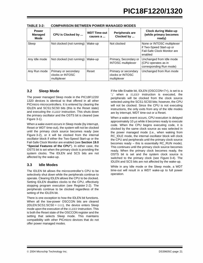
TABLE 3-2: COMPARISON BETWEEN POWER MANAGED MODES
PowerManaged
ModeCPU is Clocked by ...
WDT Time-out causes a ...
Peripherals are Clocked by ...
Clock during Wake-up (while primary becomes
ready)
Sleep Not clocked (not running) Wake-up Not clocked None or INTOSC multiplexer if Two-Speed Start-up or Fail-Safe Clock Monitor are enabled
Any Idle mode Not clocked (not running) Wake-up Primary, Secondary or INTOSC multiplexer
Unchanged from Idle mode (CPU operates as in corresponding Run mode)
Any Run mode Primary or secondary clocks or INTOSC multiplexer
Reset Primary or secondary clocks or INTOSC multiplexer
Unchanged from Run mode
2004 Microchip Technology Inc. DS39605C-page 21

PIC18F1220/1320
FIGURE 3-1: TIMING TRANSITION FOR ENTRY TO SLEEP MODE
FIGURE 3-2: TRANSITION TIMING FOR WAKE FROM SLEEP (HSPLL)
Q4Q3Q2
OSC1
Peripheral
Sleep
Program
Q1Q1
Counter
Clock
CPUClock
PC + 2PC
Q3 Q4 Q1 Q2
OSC1
Peripheral
Program PC
PLL Clock
Q3 Q4
Output
CPU Clock
Q1 Q2 Q3 Q4 Q1 Q2
Clock
Counter PC + 8PC + 6
Q1 Q2 Q3 Q4
Wake Event
Note 1: TOST = 1024 TOSC; TPLL = 2 ms (approx). These intervals are not shown to scale.
TOST(1)TPLL(1)
OSTS bit Set
PC + 4PC + 2
DS39605C-page 22 2004 Microchip Technology Inc.

PIC18F1220/1320
3.3.1 PRI_IDLE MODE
This mode is unique among the three Low-Power Idlemodes, in that it does not disable the primary systemclock. For timing sensitive applications, this allows forthe fastest resumption of device operation with its moreaccurate primary clock source, since the clock sourcedoes not have to “warm up” or transition from anotheroscillator.
PRI_IDLE mode is entered by setting the IDLEN bit,clearing the SCS bits and executing a SLEEP instruc-tion. Although the CPU is disabled, the peripheralscontinue to be clocked from the primary clock sourcespecified in Configuration Register 1H. The OSTS bitremains set in PRI_IDLE mode (see Figure 3-3).
When a wake event occurs, the CPU is clocked fromthe primary clock source. A delay of approximately10 µs is required between the wake event and codeexecution starts. This is required to allow the CPU tobecome ready to execute instructions. After the wake-up, the OSTS bit remains set. The IDLEN and SCS bitsare not affected by the wake-up (see Figure 3-4).
FIGURE 3-3: TRANSITION TIMING TO PRI_IDLE MODE
FIGURE 3-4: TRANSITION TIMING FOR WAKE FROM PRI_IDLE MODE
Q1
Peripheral
Program PC PC + 2
OSC1
Q3 Q4 Q1
CPU Clock
Clock
Counter
Q2
OSC1
Peripheral
Program PC
CPU Clock
PC + 2
Q1 Q3 Q4
Clock
Counter
Q2
Wake Event
CPU Start-up Delay
2004 Microchip Technology Inc. DS39605C-page 23
PIC18F1220/1320
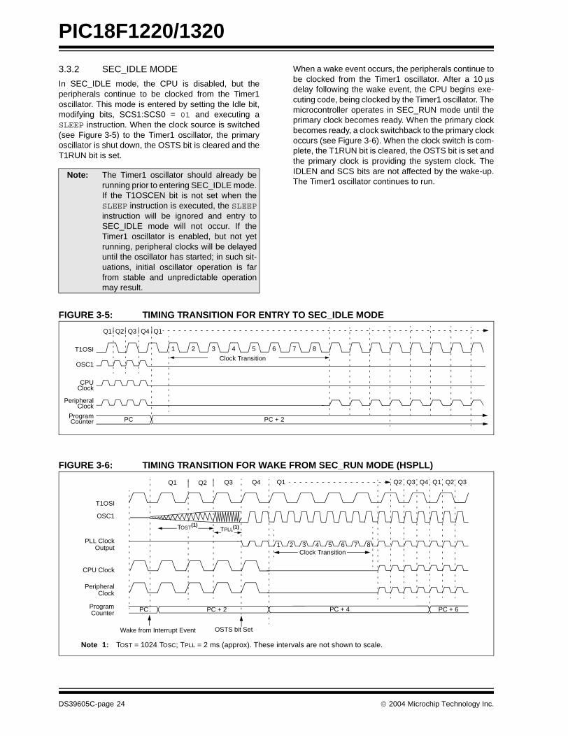
3.3.2 SEC_IDLE MODE
In SEC_IDLE mode, the CPU is disabled, but theperipherals continue to be clocked from the Timer1oscillator. This mode is entered by setting the Idle bit,modifying bits, SCS1:SCS0 = 01 and executing aSLEEP instruction. When the clock source is switched(see Figure 3-5) to the Timer1 oscillator, the primaryoscillator is shut down, the OSTS bit is cleared and theT1RUN bit is set.
When a wake event occurs, the peripherals continue tobe clocked from the Timer1 oscillator. After a 10 µsdelay following the wake event, the CPU begins exe-cuting code, being clocked by the Timer1 oscillator. Themicrocontroller operates in SEC_RUN mode until theprimary clock becomes ready. When the primary clockbecomes ready, a clock switchback to the primary clockoccurs (see Figure 3-6). When the clock switch is com-plete, the T1RUN bit is cleared, the OSTS bit is set andthe primary clock is providing the system clock. TheIDLEN and SCS bits are not affected by the wake-up.The Timer1 oscillator continues to run.
FIGURE 3-5: TIMING TRANSITION FOR ENTRY TO SEC_IDLE MODE
FIGURE 3-6: TIMING TRANSITION FOR WAKE FROM SEC_RUN MODE (HSPLL)
Note: The Timer1 oscillator should already berunning prior to entering SEC_IDLE mode.If the T1OSCEN bit is not set when theSLEEP instruction is executed, the SLEEPinstruction will be ignored and entry toSEC_IDLE mode will not occur. If theTimer1 oscillator is enabled, but not yetrunning, peripheral clocks will be delayeduntil the oscillator has started; in such sit-uations, initial oscillator operation is farfrom stable and unpredictable operationmay result.
Q4Q3Q2
OSC1
Peripheral
Program
Q1
T1OSI
Q1
Counter
Clock
CPUClock
PC + 2PC
1 2 3 4 5 6 7 8
Clock Transition
Q1 Q3 Q4
OSC1
Peripheral
Program PC PC + 2
T1OSI
PLL Clock
Q1
PC + 6
Q2
Output
Q3 Q4 Q1
CPU Clock
PC + 4
Clock
Counter
Q2 Q2 Q3
Note 1: TOST = 1024 TOSC; TPLL = 2 ms (approx). These intervals are not shown to scale.
Wake from Interrupt Event
TPLL(1)
1 2 3 4 5 6 7 8Clock Transition
OSTS bit Set
TOST(1)
DS39605C-page 24 2004 Microchip Technology Inc.

PIC18F1220/1320
3.3.3 RC_IDLE MODE
In RC_IDLE mode, the CPU is disabled, but the periph-erals continue to be clocked from the internal oscillatorblock using the INTOSC multiplexer. This mode allowsfor controllable power conservation during Idle periods.
This mode is entered by setting the IDLEN bit, settingSCS1 (SCS0 is ignored) and executing a SLEEPinstruction. The INTOSC multiplexer may be used toselect a higher clock frequency by modifying the IRCFbits before executing the SLEEP instruction. When theclock source is switched to the INTOSC multiplexer(see Figure 3-7), the primary oscillator is shut downand the OSTS bit is cleared.
If the IRCF bits are set to a non-zero value (thus,enabling the INTOSC output), the IOFS bit becomesset after the INTOSC output becomes stable, in about1 ms. Clocks to the peripherals continue while theINTOSC source stabilizes. If the IRCF bits werepreviously at a non-zero value before the SLEEP
instruction was executed and the INTOSC source wasalready stable, the IOFS bit will remain set. If the IRCFbits are all clear, the INTOSC output is not enabled andthe IOFS bit will remain clear; there will be no indicationof the current clock source.
When a wake event occurs, the peripherals continue tobe clocked from the INTOSC multiplexer. After a 10 µsdelay following the wake event, the CPU begins exe-cuting code, being clocked by the INTOSC multiplexer.The microcontroller operates in RC_RUN mode untilthe primary clock becomes ready. When the primaryclock becomes ready, a clock switchback to the primaryclock occurs (see Figure 3-8). When the clock switch iscomplete, the IOFS bit is cleared, the OSTS bit is setand the primary clock is providing the system clock.The IDLEN and SCS bits are not affected by the wake-up. The INTRC source will continue to run if either theWDT or the Fail-Safe Clock Monitor is enabled.
FIGURE 3-7: TIMING TRANSITION TO RC_IDLE MODE
FIGURE 3-8: TIMING TRANSITION FOR WAKE FROM RC_RUN MODE (RC_RUN TO PRI_RUN)
Q4Q3Q2
OSC1
Peripheral
Program
Q1
INTRC
Q1
Counter
Clock
CPUClock
PC + 2PC
1 2 3 4 5 6 7 8
Clock Transition
Q1 Q3 Q4
OSC1
Peripheral
Program PC PC + 2
INTOSC
PLL Clock
Q1
PC + 6
Q2
Output
Q3 Q4 Q1
CPU Clock
PC + 4
Clock
Counter
Q2 Q2 Q3
Note 1: TOST = 1024 TOSC; TPLL = 2 ms (approx). These intervals are not shown to scale.
Wake from Interrupt Event
TOST(1)TPLL(1)
1 2 3 4 5 6 7 8Clock Transition
OSTS bit Set
Multiplexer
Q4
2004 Microchip Technology Inc. DS39605C-page 25

PIC18F1220/1320
3.4 Run Modes
If the IDLEN bit is clear when a SLEEP instruction isexecuted, the CPU and peripherals are both clockedfrom the source selected using the SCS1:SCS0 bits.While these operating modes may not afford the powerconservation of Idle or Sleep modes, they do allow thedevice to continue executing instructions by using alower frequency clock source. RC_RUN mode alsooffers the possibility of executing code at a frequencygreater than the primary clock.
Wake-up from a power managed Run mode can betriggered by an interrupt, or any Reset, to return to fullpower operation. As the CPU is executing code in Runmodes, several additional exits from Run modes arepossible. They include exit to Sleep mode, exit to a cor-responding Idle mode and exit by executing a RESETinstruction. While the device is in any of the powermanaged Run modes, a WDT time-out will result in aWDT Reset.
3.4.1 PRI_RUN MODE
The PRI_RUN mode is the normal full power executionmode. If the SLEEP instruction is never executed, themicrocontroller operates in this mode (a SLEEP instruc-tion is executed to enter all other power managedmodes). All other power managed modes exit toPRI_RUN mode when an interrupt or WDT time-outoccur.
There is no entry to PRI_RUN mode. The OSTS bit isset. The IOFS bit may be set if the internal oscillatorblock is the primary clock source (see Section 2.7.1“Oscillator Control Register”).
3.4.2 SEC_RUN MODE
The SEC_RUN mode is the compatible mode to the“clock switching” feature offered in other PIC18devices. In this mode, the CPU and peripherals areclocked from the Timer1 oscillator. This gives users theoption of lower power consumption while still using ahigh accuracy clock source.
SEC_RUN mode is entered by clearing the IDLEN bit,setting SCS1:SCS0 = 01 and executing a SLEEPinstruction. The system clock source is switched to theTimer1 oscillator (see Figure 3-9), the primary oscilla-tor is shut down, the T1RUN bit (T1CON<6>) is set andthe OSTS bit is cleared.
When a wake event occurs, the peripherals and CPUcontinue to be clocked from the Timer1 oscillator whilethe primary clock is started. When the primary clockbecomes ready, a clock switchback to the primary clockoccurs (see Figure 3-6). When the clock switch is com-plete, the T1RUN bit is cleared, the OSTS bit is set andthe primary clock is providing the system clock. TheIDLEN and SCS bits are not affected by the wake-up.The Timer1 oscillator continues to run.
Firmware can force an exit from SEC_RUN mode. Byclearing the T1OSCEN bit (T1CON<3>), an exit fromSEC_RUN back to normal full power operation is trig-gered. The Timer1 oscillator will continue to run andprovide the system clock, even though the T1OSCENbit is cleared. The primary clock is started. When theprimary clock becomes ready, a clock switchback to theprimary clock occurs (see Figure 3-6). When the clockswitch is complete, the Timer1 oscillator is disabled, theT1RUN bit is cleared, the OSTS bit is set and the pri-mary clock is providing the system clock. The IDLENand SCS bits are not affected by the wake-up.
FIGURE 3-9: TIMING TRANSITION FOR ENTRY TO SEC_RUN MODE
Note: The Timer1 oscillator should already berunning prior to entering SEC_RUN mode.If the T1OSCEN bit is not set when theSLEEP instruction is executed, the SLEEPinstruction will be ignored and entry toSEC_RUN mode will not occur. If theTimer1 oscillator is enabled, but not yetrunning, system clocks will be delayeduntil the oscillator has started; in suchsituations, initial oscillator operation is farfrom stable and unpredictable operationmay result.
Q4Q3Q2
OSC1
Peripheral
Program
Q1
T1OSI
Q1
Counter
Clock
CPUClock
PC + 2PC
1 2 3 4 5 6 7 8
Clock Transition
Q4Q3Q2 Q1 Q3Q2
PC + 2
DS39605C-page 26 2004 Microchip Technology Inc.

PIC18F1220/1320
3.4.3 RC_RUN MODE
In RC_RUN mode, the CPU and peripherals areclocked from the internal oscillator block using theINTOSC multiplexer and the primary clock is shutdown. When using the INTRC source, this mode pro-vides the best power conservation of all the Runmodes, while still executing code. It works well for userapplications which are not highly timing sensitive, or donot require high-speed clocks at all times.
If the primary clock source is the internal oscillatorblock (either of the INTIO1 or INTIO2 oscillators), thereare no distinguishable differences between PRI_RUNand RC_RUN modes during execution. However, aclock switch delay will occur during entry to and exitfrom RC_RUN mode. Therefore, if the primary clocksource is the internal oscillator block, the use ofRC_RUN mode is not recommended.
This mode is entered by clearing the IDLEN bit, settingSCS1 (SCS0 is ignored) and executing a SLEEPinstruction. The IRCF bits may select the clockfrequency before the SLEEP instruction is executed.When the clock source is switched to the INTOSCmultiplexer (see Figure 3-10), the primary oscillator isshut down and the OSTS bit is cleared.
The IRCF bits may be modified at any time to immedi-ately change the system clock speed. Executing aSLEEP instruction is not required to select a new clockfrequency from the INTOSC multiplexer.
If the IRCF bits are all clear, the INTOSC output is notenabled and the IOFS bit will remain clear; there will beno indication of the current clock source. The INTRCsource is providing the system clocks.
If the IRCF bits are changed from all clear (thus,enabling the INTOSC output), the IOFS bit becomesset after the INTOSC output becomes stable. Clocks tothe system continue while the INTOSC sourcestabilizes, in approximately 1 ms.
If the IRCF bits were previously at a non-zero valuebefore the SLEEP instruction was executed and theINTOSC source was already stable, the IOFS bit willremain set.
When a wake event occurs, the system continues to beclocked from the INTOSC multiplexer while the primaryclock is started. When the primary clock becomesready, a clock switch to the primary clock occurs (seeFigure 3-8). When the clock switch is complete, theIOFS bit is cleared, the OSTS bit is set and the primaryclock is providing the system clock. The IDLEN andSCS bits are not affected by the wake-up. The INTRCsource will continue to run if either the WDT or theFail-Safe Clock Monitor is enabled.
FIGURE 3-10: TIMING TRANSITION TO RC_RUN MODE
Note: Caution should be used when modifying asingle IRCF bit. If VDD is less than 3V, it ispossible to select a higher clock speedthan is supported by the low VDD.Improper device operation may result ifthe VDD/FOSC specifications are violated.
Q3Q2Q1
OSC1
Peripheral
Program
Q4
INTRC
Q4
Counter
Clock
CPUClock
PC + 2PC
1 2 3 4 5 6 7 8
Clock Transition
Q3Q2Q1 Q4 Q2Q1 Q3
PC + 4
2004 Microchip Technology Inc. DS39605C-page 27
PIC18F1220/1320
3.4.4 EXIT TO IDLE MODE
An exit from a power managed Run mode to itscorresponding Idle mode is executed by setting theIDLEN bit and executing a SLEEP instruction. The CPUis halted at the beginning of the instruction following theSLEEP instruction. There are no changes to any of theclock source status bits (OSTS, IOFS or T1RUN).While the CPU is halted, the peripherals continue to beclocked from the previously selected clock source.
3.4.5 EXIT TO SLEEP MODE
An exit from a power managed Run mode to Sleepmode is executed by clearing the IDLEN andSCS1:SCS0 bits and executing a SLEEP instruction.The code is no different than the method used to invokeSleep mode from the normal operating (full power)mode.
The primary clock and internal oscillator block aredisabled. The INTRC will continue to operate if theWDT is enabled. The Timer1 oscillator will continue torun, if enabled in the T1CON register (Register 12-1).All clock source status bits are cleared (OSTS, IOFSand T1RUN).
3.5 Wake from Power Managed Modes
An exit from any of the power managed modes is trig-gered by an interrupt, a Reset or a WDT time-out. Thissection discusses the triggers that cause exits frompower managed modes. The clocking subsystemactions are discussed in each of the power managedmodes (see Sections 3.2 through 3.4).
Device behavior during Low-Power mode exits issummarized in Table 3-3.
3.5.1 EXIT BY INTERRUPT
Any of the available interrupt sources can cause thedevice to exit a power managed mode and resume fullpower operation. To enable this functionality, an inter-rupt source must be enabled by setting its enable bit inone of the INTCON or PIE registers. The exit sequenceis initiated when the corresponding interrupt flag bit isset. On all exits from Low-Power mode by interrupt,code execution branches to the interrupt vector if theGIE/GIEH bit (INTCON<7>) is set. Otherwise, codeexecution continues or resumes without branching(see Section 9.0 “Interrupts”).
Note: If application code is timing sensitive, itshould wait for the OSTS bit to become setbefore continuing. Use the interval duringthe low-power exit sequence (beforeOSTS is set) to perform timing insensitive“housekeeping” tasks.
DS39605C-page 28 2004 Microchip Technology Inc.
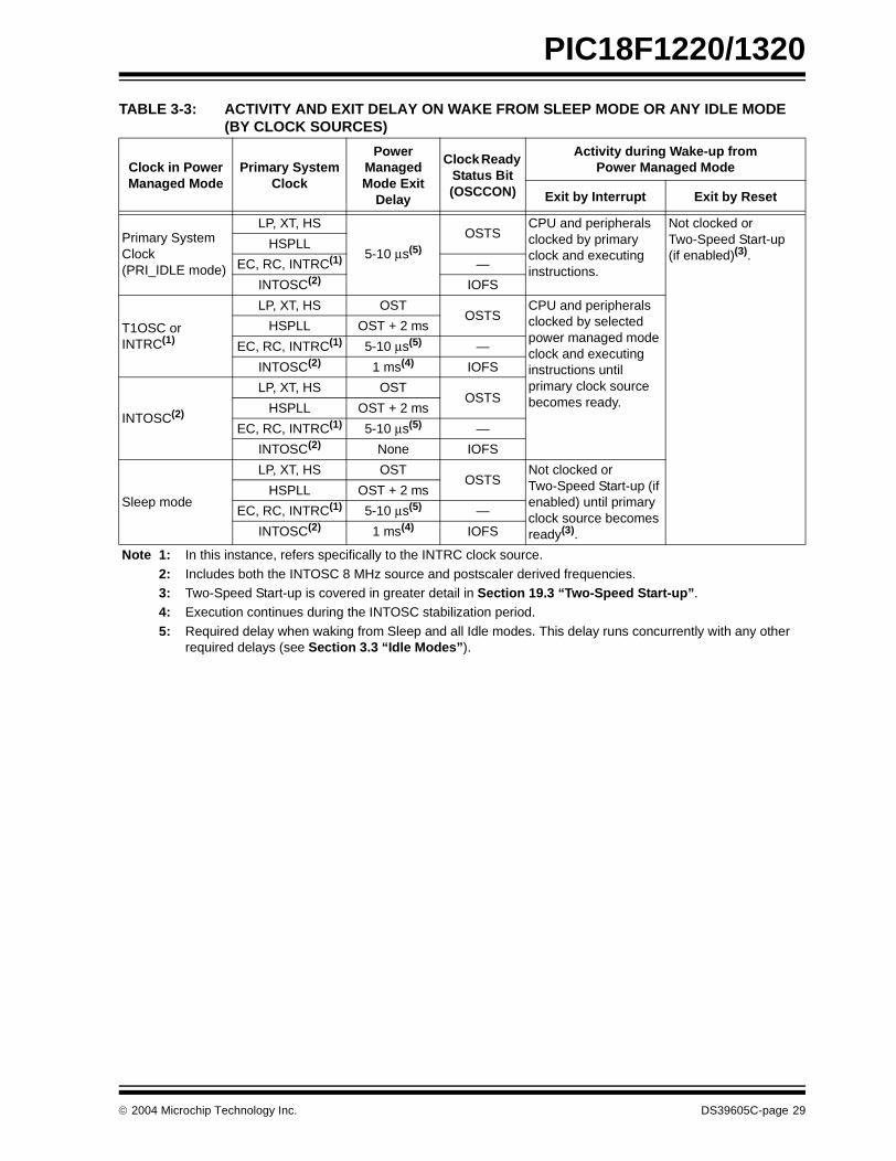
PIC18F1220/1320
TABLE 3-3: ACTIVITY AND EXIT DELAY ON WAKE FROM SLEEP MODE OR ANY IDLE MODE(BY CLOCK SOURCES)
Clock in Power Managed Mode
Primary System Clock
Power Managed Mode Exit
Delay
Clock Ready Status Bit (OSCCON)
Activity during Wake-up from Power Managed Mode
Exit by Interrupt Exit by Reset
Primary System Clock(PRI_IDLE mode)
LP, XT, HS
5-10 µs(5)OSTS
CPU and peripherals clocked by primary clock and executing instructions.
Not clocked or Two-Speed Start-up (if enabled)(3).
HSPLL
EC, RC, INTRC(1) —
INTOSC(2) IOFS
T1OSC or INTRC(1)
LP, XT, HS OSTOSTS
CPU and peripherals clocked by selected power managed mode clock and executing instructions until primary clock source becomes ready.
HSPLL OST + 2 ms
EC, RC, INTRC(1) 5-10 µs(5) —
INTOSC(2) 1 ms(4) IOFS
INTOSC(2)
LP, XT, HS OSTOSTS
HSPLL OST + 2 ms
EC, RC, INTRC(1) 5-10 µs(5) —
INTOSC(2) None IOFS
Sleep mode
LP, XT, HS OSTOSTS
Not clocked or Two-Speed Start-up (if enabled) until primary clock source becomes ready(3).
HSPLL OST + 2 ms
EC, RC, INTRC(1) 5-10 µs(5) —
INTOSC(2) 1 ms(4) IOFS
Note 1: In this instance, refers specifically to the INTRC clock source.
2: Includes both the INTOSC 8 MHz source and postscaler derived frequencies.3: Two-Speed Start-up is covered in greater detail in Section 19.3 “Two-Speed Start-up”.4: Execution continues during the INTOSC stabilization period.
5: Required delay when waking from Sleep and all Idle modes. This delay runs concurrently with any other required delays (see Section 3.3 “Idle Modes”).
2004 Microchip Technology Inc. DS39605C-page 29
PIC18F1220/1320
3.5.2 EXIT BY RESET
Normally, the device is held in Reset by the OscillatorStart-up Timer (OST) until the primary clock (defined inConfiguration Register 1H) becomes ready. At thattime, the OSTS bit is set and the device beginsexecuting code.
Code execution can begin before the primary clockbecomes ready. If either the Two-Speed Start-up (seeSection 19.3 “Two-Speed Start-up”) or Fail-SafeClock Monitor (see Section 19.4 “Fail-Safe ClockMonitor”) are enabled in Configuration Register 1H,the device may begin execution as soon as the Resetsource has cleared. Execution is clocked by theINTOSC multiplexer driven by the internal oscillatorblock. Since the OSCCON register is cleared followingall Resets, the INTRC clock source is selected. Ahigher speed clock may be selected by modifying theIRCF bits in the OSCCON register. Execution isclocked by the internal oscillator block until either theprimary clock becomes ready, or a power managedmode is entered before the primary clock becomesready; the primary clock is then shut down.
3.5.3 EXIT BY WDT TIME-OUT
A WDT time-out will cause different actions, dependingon which power managed mode the device is in whenthe time-out occurs.
If the device is not executing code (all Idle modes andSleep mode), the time-out will result in a wake from thepower managed mode (see Sections 3.2 through 3.4).
If the device is executing code (all Run modes), thetime-out will result in a WDT Reset (see Section 19.2“Watchdog Timer (WDT)”).
The WDT timer and postscaler are cleared byexecuting a SLEEP or CLRWDT instruction, the loss of acurrently selected clock source (if the Fail-Safe ClockMonitor is enabled) and modifying the IRCF bits in theOSCCON register if the internal oscillator block is thesystem clock source.
3.5.4 EXIT WITHOUT AN OSCILLATOR START-UP DELAY
Certain exits from power managed modes do notinvoke the OST at all. These are:
• PRI_IDLE mode, where the primary clock source is not stopped; or
• the primary clock source is not any of LP, XT, HS or HSPLL modes.
In these cases, the primary clock source either doesnot require an oscillator start-up delay, since it isalready running (PRI_IDLE), or normally does notrequire an oscillator start-up delay (RC, EC and INTIOOscillator modes).
However, a fixed delay (approximately 10 µs) followingthe wake event is required when leaving Sleep and Idlemodes. This delay is required for the CPU to preparefor execution. Instruction execution resumes on the firstclock cycle following this delay.
3.6 INTOSC Frequency Drift
The factory calibrates the internal oscillator blockoutput (INTOSC) for 8 MHz (see Table 22-6). However,this frequency may drift as VDD or temperaturechanges, which can affect the controller operation in avariety of ways.
It is possible to adjust the INTOSC frequency bymodifying the value in the OSCTUNE register(Register 2-1). This has the side effect that the INTRCclock source frequency is also affected. However, thefeatures that use the INTRC source often do not requirean exact frequency. These features include the Fail-SafeClock Monitor, the Watchdog Timer and the RC_RUN/RC_IDLE modes when the INTRC clock source isselected.
Being able to adjust the INTOSC requires knowingwhen an adjustment is required, in which direction itshould be made and in some cases, how large achange is needed. Three examples follow but othertechniques may be used.
DS39605C-page 30 2004 Microchip Technology Inc.
PIC18F1220/1320
3.6.1 EXAMPLE – EUSART
An adjustment may be indicated when the EUSARTbegins to generate framing errors, or receives data witherrors while in Asynchronous mode. Framing errorsindicate that the system clock frequency is too high –try decrementing the value in the OSCTUNE register toreduce the system clock frequency. Errors in data maysuggest that the system clock speed is too low –increment OSCTUNE.
3.6.2 EXAMPLE – TIMERS
This technique compares system clock speed to somereference clock. Two timers may be used; one timer isclocked by the peripheral clock, while the other isclocked by a fixed reference source, such as theTimer1 oscillator.
Both timers are cleared, but the timer clocked by thereference generates interrupts. When an interruptoccurs, the internally clocked timer is read and bothtimers are cleared. If the internally clocked timer valueis greater than expected, then the internal oscillatorblock is running too fast – decrement OSCTUNE.
3.6.3 EXAMPLE – CCP IN CAPTURE MODE
A CCP module can use free running Timer1 (orTimer3), clocked by the internal oscillator block and anexternal event with a known period (i.e., AC powerfrequency). The time of the first event is captured in theCCPRxH:CCPRxL registers and is recorded for uselater. When the second event causes a capture, thetime of the first event is subtracted from the time of thesecond event. Since the period of the external event isknown, the time difference between events can becalculated.
If the measured time is much greater than thecalculated time, the internal oscillator block is runningtoo fast – decrement OSCTUNE. If the measured timeis much less than the calculated time, the internaloscillator block is running too slow – incrementOSCTUNE.
2004 Microchip Technology Inc. DS39605C-page 31

PIC18F1220/1320
NOTES:
DS39605C-page 32 2004 Microchip Technology Inc.
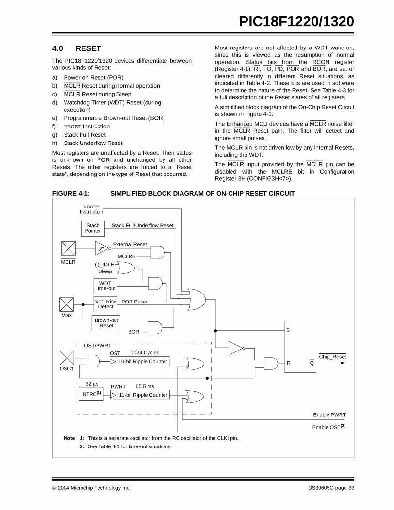
PIC18F1220/1320
4.0 RESET
The PIC18F1220/1320 devices differentiate betweenvarious kinds of Reset:
a) Power-on Reset (POR)
b) MCLR Reset during normal operationc) MCLR Reset during Sleep d) Watchdog Timer (WDT) Reset (during
execution)e) Programmable Brown-out Reset (BOR)
f) RESET Instructiong) Stack Full Reseth) Stack Underflow Reset
Most registers are unaffected by a Reset. Their statusis unknown on POR and unchanged by all otherResets. The other registers are forced to a “Resetstate”, depending on the type of Reset that occurred.
Most registers are not affected by a WDT wake-up,since this is viewed as the resumption of normaloperation. Status bits from the RCON register(Register 4-1), RI, TO, PD, POR and BOR, are set orcleared differently in different Reset situations, asindicated in Table 4-2. These bits are used in softwareto determine the nature of the Reset. See Table 4-3 fora full description of the Reset states of all registers.
A simplified block diagram of the On-Chip Reset Circuitis shown in Figure 4-1.
The Enhanced MCU devices have a MCLR noise filterin the MCLR Reset path. The filter will detect andignore small pulses.
The MCLR pin is not driven low by any internal Resets,including the WDT.
The MCLR input provided by the MCLR pin can bedisabled with the MCLRE bit in ConfigurationRegister 3H (CONFIG3H<7>).
FIGURE 4-1: SIMPLIFIED BLOCK DIAGRAM OF ON-CHIP RESET CIRCUIT
S
R Q
External Reset
MCLR
VDD
OSC1
WDTTime-out
VDD RiseDetect
OST/PWRT
INTRC(1)
POR Pulse
OST
10-bit Ripple Counter
PWRT
Chip_Reset
11-bit Ripple Counter
Enable OST(2)
Enable PWRT
Note 1: This is a separate oscillator from the RC oscillator of the CLKI pin.
2: See Table 4-1 for time-out situations.
Brown-outReset
BOR
RESETInstruction
StackPointer
Stack Full/Underflow Reset
Sleep( )_IDLE
1024 Cycles
65.5 ms32 µs
MCLRE
2004 Microchip Technology Inc. DS39605C-page 33
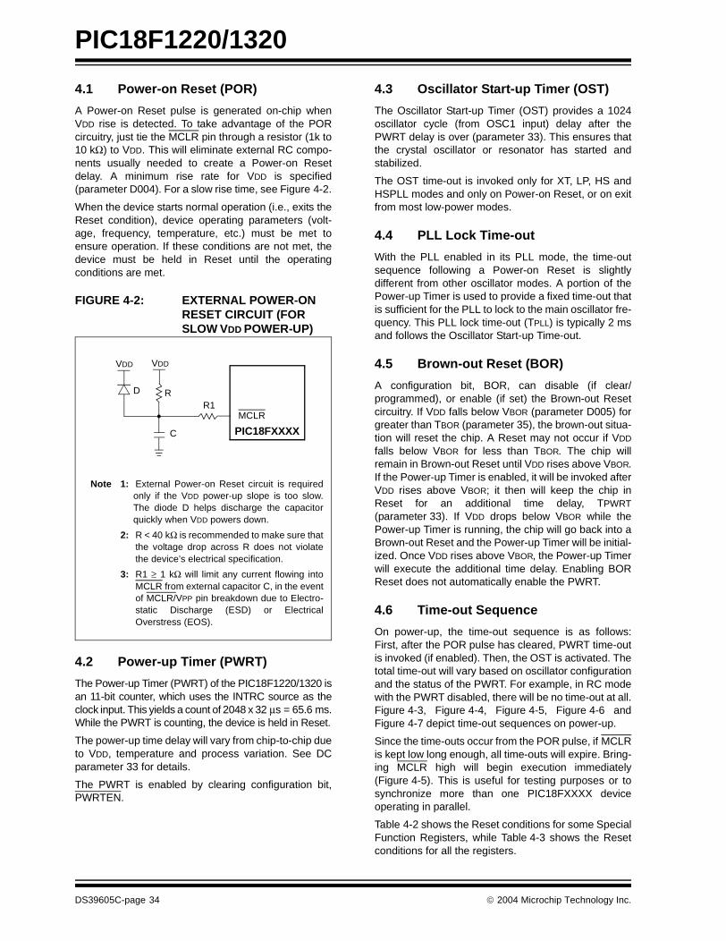
PIC18F1220/1320
4.1 Power-on Reset (POR)
A Power-on Reset pulse is generated on-chip whenVDD rise is detected. To take advantage of the PORcircuitry, just tie the MCLR pin through a resistor (1k to10 kΩ) to VDD. This will eliminate external RC compo-nents usually needed to create a Power-on Resetdelay. A minimum rise rate for VDD is specified(parameter D004). For a slow rise time, see Figure 4-2.
When the device starts normal operation (i.e., exits theReset condition), device operating parameters (volt-age, frequency, temperature, etc.) must be met toensure operation. If these conditions are not met, thedevice must be held in Reset until the operatingconditions are met.
FIGURE 4-2: EXTERNAL POWER-ON RESET CIRCUIT (FOR SLOW VDD POWER-UP)
4.2 Power-up Timer (PWRT)
The Power-up Timer (PWRT) of the PIC18F1220/1320 isan 11-bit counter, which uses the INTRC source as theclock input. This yields a count of 2048 x 32 µs = 65.6 ms.While the PWRT is counting, the device is held in Reset.
The power-up time delay will vary from chip-to-chip dueto VDD, temperature and process variation. See DCparameter 33 for details.
The PWRT is enabled by clearing configuration bit,PWRTEN.
4.3 Oscillator Start-up Timer (OST)
The Oscillator Start-up Timer (OST) provides a 1024oscillator cycle (from OSC1 input) delay after thePWRT delay is over (parameter 33). This ensures thatthe crystal oscillator or resonator has started andstabilized.
The OST time-out is invoked only for XT, LP, HS andHSPLL modes and only on Power-on Reset, or on exitfrom most low-power modes.
4.4 PLL Lock Time-out
With the PLL enabled in its PLL mode, the time-outsequence following a Power-on Reset is slightlydifferent from other oscillator modes. A portion of thePower-up Timer is used to provide a fixed time-out thatis sufficient for the PLL to lock to the main oscillator fre-quency. This PLL lock time-out (TPLL) is typically 2 msand follows the Oscillator Start-up Time-out.
4.5 Brown-out Reset (BOR)
A configuration bit, BOR, can disable (if clear/programmed), or enable (if set) the Brown-out Resetcircuitry. If VDD falls below VBOR (parameter D005) forgreater than TBOR (parameter 35), the brown-out situa-tion will reset the chip. A Reset may not occur if VDD
falls below VBOR for less than TBOR. The chip willremain in Brown-out Reset until VDD rises above VBOR.If the Power-up Timer is enabled, it will be invoked afterVDD rises above VBOR; it then will keep the chip inReset for an additional time delay, TPWRT(parameter 33). If VDD drops below VBOR while thePower-up Timer is running, the chip will go back into aBrown-out Reset and the Power-up Timer will be initial-ized. Once VDD rises above VBOR, the Power-up Timerwill execute the additional time delay. Enabling BORReset does not automatically enable the PWRT.
4.6 Time-out Sequence
On power-up, the time-out sequence is as follows:First, after the POR pulse has cleared, PWRT time-outis invoked (if enabled). Then, the OST is activated. Thetotal time-out will vary based on oscillator configurationand the status of the PWRT. For example, in RC modewith the PWRT disabled, there will be no time-out at all.Figure 4-3, Figure 4-4, Figure 4-5, Figure 4-6 andFigure 4-7 depict time-out sequences on power-up.
Since the time-outs occur from the POR pulse, if MCLRis kept low long enough, all time-outs will expire. Bring-ing MCLR high will begin execution immediately(Figure 4-5). This is useful for testing purposes or tosynchronize more than one PIC18FXXXX deviceoperating in parallel.
Table 4-2 shows the Reset conditions for some SpecialFunction Registers, while Table 4-3 shows the Resetconditions for all the registers.
Note 1: External Power-on Reset circuit is requiredonly if the VDD power-up slope is too slow.The diode D helps discharge the capacitorquickly when VDD powers down.
2: R < 40 kΩ is recommended to make sure thatthe voltage drop across R does not violatethe device’s electrical specification.
3: R1 ≥ 1 kΩ will limit any current flowing intoMCLR from external capacitor C, in the eventof MCLR/VPP pin breakdown due to Electro-static Discharge (ESD) or ElectricalOverstress (EOS).
C
R1RD
VDD
MCLR
PIC18FXXXX
VDD
DS39605C-page 34 2004 Microchip Technology Inc.
PIC18F1220/1320
TABLE 4-1: TIME-OUT IN VARIOUS SITUATIONS
REGISTER 4-1: RCON REGISTER BITS AND POSITIONS
TABLE 4-2: STATUS BITS, THEIR SIGNIFICANCE AND THE INITIALIZATION CONDITION FOR RCON REGISTER
OscillatorConfiguration
Power-up(2) and Brown-out Exit from Low-Power ModePWRTEN = 0 PWRTEN = 1
HSPLL 66 ms(1) + 1024 TOSC + 2 ms(2) 1024 TOSC + 2 ms(2) 1024 TOSC + 2 ms(2)
HS, XT, LP 66 ms(1) + 1024 TOSC 1024 TOSC 1024 TOSC
EC, ECIO 66 ms(1) 5-10 µs(3) 5-10 µs(3)
RC, RCIO 66 ms(1) 5-10 µs(3) 5-10 µs(3)
INTIO1, INTIO2 66 ms(1) 5-10 µs(3) 5-10 µs(3)
Note 1: 66 ms (65.5 ms) is the nominal Power-up Timer (PWRT) delay.2: 2 ms is the nominal time required for the 4x PLL to lock.3: The program memory bias start-up time is always invoked on POR, wake-up from Sleep, or on any exit
from power managed mode that disables the CPU and instruction execution.
R/W-0 U-0 U-0 R/W-1 R/W-1 R/W-1 R/W-1 R/W-1
IPEN — — RI TO PD POR BOR
bit 7 bit 0
Note: Refer to Section 5.14 “RCON Register” for bit definitions.
ConditionProgram Counter
RCONRegister
RI TO PD POR BOR STKFUL STKUNF
Power-on Reset 0000h 0--1 1100 1 1 1 0 0 0 0
RESET Instruction 0000h 0--0 uuuu 0 u u u u u u
Brown-out 0000h 0--1 11u- 1 1 1 u 0 u u
MCLR during Power Managed Run modes
0000h 0--u 1uuu u 1 u u u u u
MCLR during Power Managed Idle modes and Sleep
0000h 0--u 10uu u 1 0 u u u u
WDT Time-out during Full Power or Power Managed Run
0000h 0--u 0uuu u 0 u u u u u
MCLR during Full Power Execution
0000h 0--u uuuu u u u u u
u u
Stack Full Reset (STVR = 1) 1 u
Stack Underflow Reset (STVR = 1)
u 1
Stack Underflow Error (not an actual Reset, STVR = 0)
0000h u--u uuuu u u u u u u 1
WDT Time-out during Power Managed Idle or Sleep
PC + 2 u--u 00uu u 0 0 u u u u
Interrupt Exit from Power Managed modes
PC + 2 u--u u0uu u u 0 u u u u
Legend: u = unchanged, x = unknown, – = unimplemented bit, read as ‘0’Note 1: When the wake-up is due to an interrupt and the GIEH or GIEL bits are set, the PC is loaded with the
interrupt vector (0x000008h or 0x000018h).
2004 Microchip Technology Inc. DS39605C-page 35
PIC18F1220/1320
TABLE 4-3: INITIALIZATION CONDITIONS FOR ALL REGISTERSRegisterApplicable
DevicesPower-on Reset,Brown-out Reset
MCLR ResetsWDT Reset
RESET InstructionStack Resets
Wake-up via WDT or Interrupt
TOSU 1220 1320 ---0 0000 ---0 0000 ---0 uuuu(3)
TOSH 1220 1320 0000 0000 0000 0000 uuuu uuuu(3)
TOSL 1220 1320 0000 0000 0000 0000 uuuu uuuu(3)
STKPTR 1220 1320 00-0 0000 00-0 0000 uu-u uuuu(3)
PCLATU 1220 1320 ---0 0000 ---0 0000 ---u uuuu
PCLATH 1220 1320 0000 0000 0000 0000 uuuu uuuu
PCL 1220 1320 0000 0000 0000 0000 PC + 2(2)
TBLPTRU 1220 1320 --00 0000 --00 0000 --uu uuuu
TBLPTRH 1220 1320 0000 0000 0000 0000 uuuu uuuu
TBLPTRL 1220 1320 0000 0000 0000 0000 uuuu uuuu
TABLAT 1220 1320 0000 0000 0000 0000 uuuu uuuu
PRODH 1220 1320 xxxx xxxx uuuu uuuu uuuu uuuu
PRODL 1220 1320 xxxx xxxx uuuu uuuu uuuu uuuu
INTCON 1220 1320 0000 000x 0000 000u uuuu uuuu(1)
INTCON2 1220 1320 1111 -1-1 1111 -1-1 uuuu -u-u(1)
INTCON3 1220 1320 11-0 0-00 11-0 0-00 uu-u u-uu(1)
INDF0 1220 1320 N/A N/A N/A
POSTINC0 1220 1320 N/A N/A N/A
POSTDEC0 1220 1320 N/A N/A N/A
PREINC0 1220 1320 N/A N/A N/A
PLUSW0 1220 1320 N/A N/A N/A
FSR0H 1220 1320 ---- 0000 ---- 0000 ---- uuuu
FSR0L 1220 1320 xxxx xxxx uuuu uuuu uuuu uuuu
WREG 1220 1320 xxxx xxxx uuuu uuuu uuuu uuuu
INDF1 1220 1320 N/A N/A N/A
POSTINC1 1220 1320 N/A N/A N/A
POSTDEC1 1220 1320 N/A N/A N/A
PREINC1 1220 1320 N/A N/A N/A
PLUSW1 1220 1320 N/A N/A N/A
FSR1H 1220 1320 ---- 0000 ---- 0000 ---- uuuu
FSR1L 1220 1320 xxxx xxxx uuuu uuuu uuuu uuuu
Legend: u = unchanged, x = unknown, - = unimplemented bit, read as ‘0’, q = value depends on condition.Shaded cells indicate conditions do not apply for the designated device.
Note 1: One or more bits in the INTCONx or PIRx registers will be affected (to cause wake-up).2: When the wake-up is due to an interrupt and the GIEL or GIEH bit is set, the PC is loaded with the
interrupt vector (0008h or 0018h).3: When the wake-up is due to an interrupt and the GIEL or GIEH bit is set, the TOSU, TOSH and TOSL are
updated with the current value of the PC. The STKPTR is modified to point to the next location in the hardware stack.
4: See Table 4-2 for Reset value for specific condition.5: Bits 6 and 7 of PORTA, LATA and TRISA are enabled, depending on the Oscillator mode selected. When
not enabled as PORTA pins, they are disabled and read ‘0’.6: Bit 5 of PORTA is enabled if MCLR is disabled.
DS39605C-page 36 2004 Microchip Technology Inc.

PIC18F1220/1320
BSR 1220 1320 ---- 0000 ---- 0000 ---- uuuu
INDF2 1220 1320 N/A N/A N/A
POSTINC2 1220 1320 N/A N/A N/A
POSTDEC2 1220 1320 N/A N/A N/A
PREINC2 1220 1320 N/A N/A N/A
PLUSW2 1220 1320 N/A N/A N/A
FSR2H 1220 1320 ---- 0000 ---- 0000 ---- uuuu
FSR2L 1220 1320 xxxx xxxx uuuu uuuu uuuu uuuu
STATUS 1220 1320 ---x xxxx ---u uuuu ---u uuuu
TMR0H 1220 1320 0000 0000 0000 0000 uuuu uuuu
TMR0L 1220 1320 xxxx xxxx uuuu uuuu uuuu uuuu
T0CON 1220 1320 1111 1111 1111 1111 uuuu uuuu
OSCCON 1220 1320 0000 q000 0000 q000 uuuu qquu
LVDCON 1220 1320 --00 0101 --00 0101 --uu uuuu
WDTCON 1220 1320 ---- ---0 ---- ---0 ---- ---u
RCON(4) 1220 1320 0--1 11q0 0--q qquu u--u qquu
TMR1H 1220 1320 xxxx xxxx uuuu uuuu uuuu uuuu
TMR1L 1220 1320 xxxx xxxx uuuu uuuu uuuu uuuu
T1CON 1220 1320 0000 0000 u0uu uuuu uuuu uuuu
TMR2 1220 1320 0000 0000 0000 0000 uuuu uuuu
PR2 1220 1320 1111 1111 1111 1111 1111 1111
T2CON 1220 1320 -000 0000 -000 0000 -uuu uuuu
ADRESH 1220 1320 xxxx xxxx uuuu uuuu uuuu uuuu
ADRESL 1220 1320 xxxx xxxx uuuu uuuu uuuu uuuu
ADCON0 1220 1320 00-0 0000 00-0 0000 uu-u uuuu
ADCON1 1220 1320 -000 0000 -000 0000 -uuu uuuu
ADCON2 1220 1320 0-00 0000 0-00 0000 u-uu uuuu
CCPR1H 1220 1320 xxxx xxxx uuuu uuuu uuuu uuuu
CCPR1L 1220 1320 xxxx xxxx uuuu uuuu uuuu uuuu
CCP1CON 1220 1320 0000 0000 0000 0000 uuuu uuuu
PWM1CON 1220 1320 0000 0000 0000 0000 uuuu uuuu
ECCPAS 1220 1320 0000 0000 0000 0000 uuuu uuuu
TABLE 4-3: INITIALIZATION CONDITIONS FOR ALL REGISTERS (CONTINUED)
RegisterApplicable
DevicesPower-on Reset,Brown-out Reset
MCLR ResetsWDT Reset
RESET InstructionStack Resets
Wake-up via WDT or Interrupt
Legend: u = unchanged, x = unknown, - = unimplemented bit, read as ‘0’, q = value depends on condition.Shaded cells indicate conditions do not apply for the designated device.
Note 1: One or more bits in the INTCONx or PIRx registers will be affected (to cause wake-up).2: When the wake-up is due to an interrupt and the GIEL or GIEH bit is set, the PC is loaded with the
interrupt vector (0008h or 0018h).3: When the wake-up is due to an interrupt and the GIEL or GIEH bit is set, the TOSU, TOSH and TOSL are
updated with the current value of the PC. The STKPTR is modified to point to the next location in the hardware stack.
4: See Table 4-2 for Reset value for specific condition.5: Bits 6 and 7 of PORTA, LATA and TRISA are enabled, depending on the Oscillator mode selected. When
not enabled as PORTA pins, they are disabled and read ‘0’.6: Bit 5 of PORTA is enabled if MCLR is disabled.
2004 Microchip Technology Inc. DS39605C-page 37

PIC18F1220/1320
TMR3H 1220 1320 xxxx xxxx uuuu uuuu uuuu uuuu
TMR3L 1220 1320 xxxx xxxx uuuu uuuu uuuu uuuu
T3CON 1220 1320 0-00 0000 u-uu uuuu u-uu uuuu
SPBRGH 1220 1320 0000 0000 0000 0000 uuuu uuuu
SPBRG 1220 1320 0000 0000 0000 0000 uuuu uuuu
RCREG 1220 1320 0000 0000 0000 0000 uuuu uuuu
TXREG 1220 1320 0000 0000 0000 0000 uuuu uuuu
TXSTA 1220 1320 0000 0010 0000 0010 uuuu uuuu
RCSTA 1220 1320 0000 000x 0000 000x uuuu uuuu
BAUDCTL 1220 1320 -1-1 0-00 -1-1 0-00 -u-u u-uu
EEADR 1220 1320 0000 0000 0000 0000 uuuu uuuu
EEDATA 1220 1320 0000 0000 0000 0000 uuuu uuuu
EECON2 1220 1320 0000 0000 0000 0000 0000 0000
EECON1 1220 1320 xx-0 x000 uu-0 u000 uu-0 u000
IPR2 1220 1320 1--1 -11- 1--1 -11- u--u -uu-
PIR2 1220 1320 0--0 -00- 0--0 -00- u--u -uu-(1)
PIE2 1220 1320 0--0 -00- 0--0 -00- u--u -uu-
IPR1 1220 1320 -111 -111 -111 -111 -uuu -uuu
PIR1 1220 1320 -000 -000 -000 -000 -uuu -uuu(1)
PIE1 1220 1320 -000 -000 -000 -000 -uuu -uuu
OSCTUNE 1220 1320 --00 0000 --00 0000 --uu uuuu
TRISB 1220 1320 1111 1111 1111 1111 uuuu uuuu
TRISA(5) 1220 1320 11-1 1111(5) 11-1 1111(5) uu-u uuuu(5)
LATB 1220 1320 xxxx xxxx uuuu uuuu uuuu uuuu
LATA(5) 1220 1320 xx-x xxxx(5) uu-u uuuu(5) uu-u uuuu(5)
PORTB 1220 1320 xxxx xxxx uuuu uuuu uuuu uuuu
PORTA(5,6) 1220 1320 xx0x 0000(5,6) uu0u 0000(5,6) uuuu uuuu(5,6)
TABLE 4-3: INITIALIZATION CONDITIONS FOR ALL REGISTERS (CONTINUED)
RegisterApplicable
DevicesPower-on Reset,Brown-out Reset
MCLR ResetsWDT Reset
RESET InstructionStack Resets
Wake-up via WDT or Interrupt
Legend: u = unchanged, x = unknown, - = unimplemented bit, read as ‘0’, q = value depends on condition.Shaded cells indicate conditions do not apply for the designated device.
Note 1: One or more bits in the INTCONx or PIRx registers will be affected (to cause wake-up).2: When the wake-up is due to an interrupt and the GIEL or GIEH bit is set, the PC is loaded with the
interrupt vector (0008h or 0018h).3: When the wake-up is due to an interrupt and the GIEL or GIEH bit is set, the TOSU, TOSH and TOSL are
updated with the current value of the PC. The STKPTR is modified to point to the next location in the hardware stack.
4: See Table 4-2 for Reset value for specific condition.5: Bits 6 and 7 of PORTA, LATA and TRISA are enabled, depending on the Oscillator mode selected. When
not enabled as PORTA pins, they are disabled and read ‘0’.6: Bit 5 of PORTA is enabled if MCLR is disabled.
DS39605C-page 38 2004 Microchip Technology Inc.
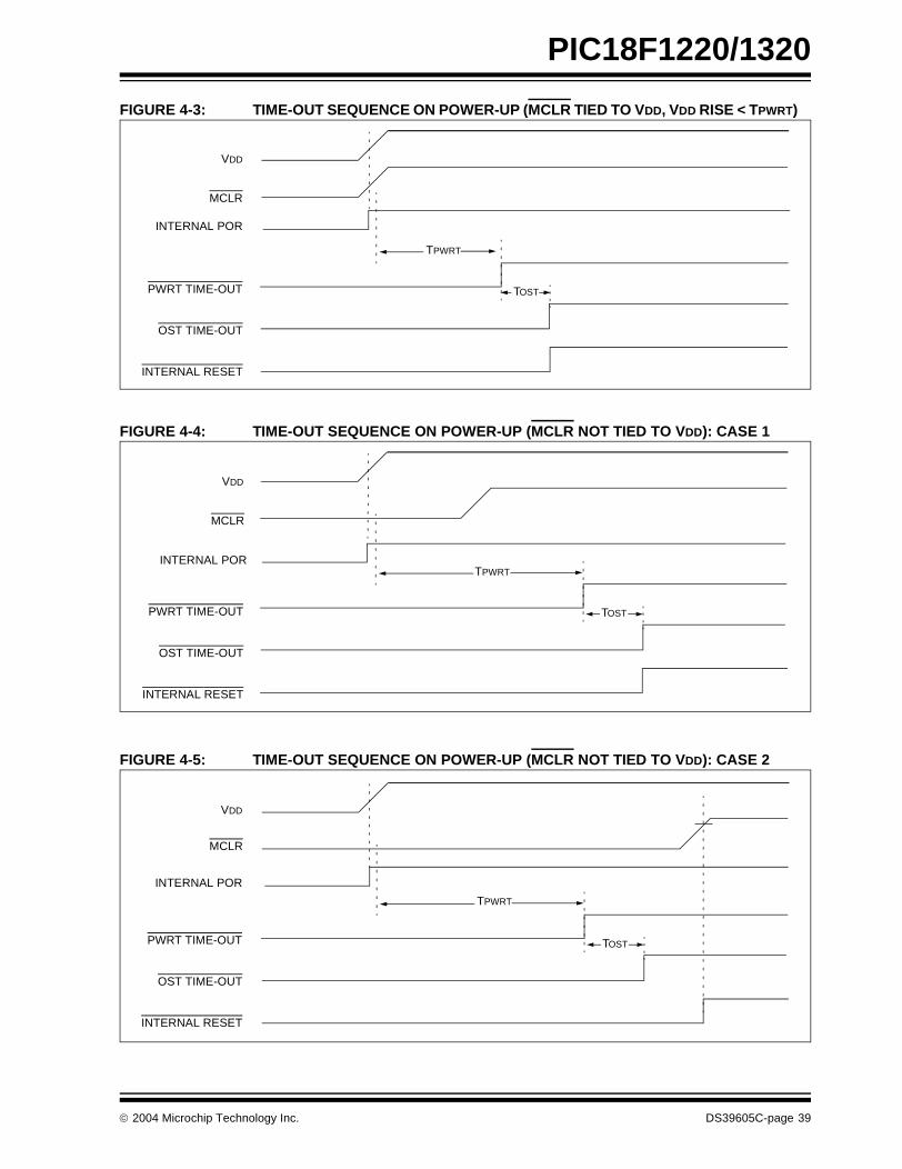
PIC18F1220/1320
FIGURE 4-3: TIME-OUT SEQUENCE ON POWER-UP (MCLR TIED TO VDD, VDD RISE < TPWRT)
FIGURE 4-4: TIME-OUT SEQUENCE ON POWER-UP (MCLR NOT TIED TO VDD): CASE 1
FIGURE 4-5: TIME-OUT SEQUENCE ON POWER-UP (MCLR NOT TIED TO VDD): CASE 2
TPWRT
TOST
VDD
MCLR
INTERNAL POR
PWRT TIME-OUT
OST TIME-OUT
INTERNAL RESET
TPWRT
TOST
VDD
MCLR
INTERNAL POR
PWRT TIME-OUT
OST TIME-OUT
INTERNAL RESET
VDD
MCLR
INTERNAL POR
PWRT TIME-OUT
OST TIME-OUT
INTERNAL RESET
TPWRT
TOST
2004 Microchip Technology Inc. DS39605C-page 39
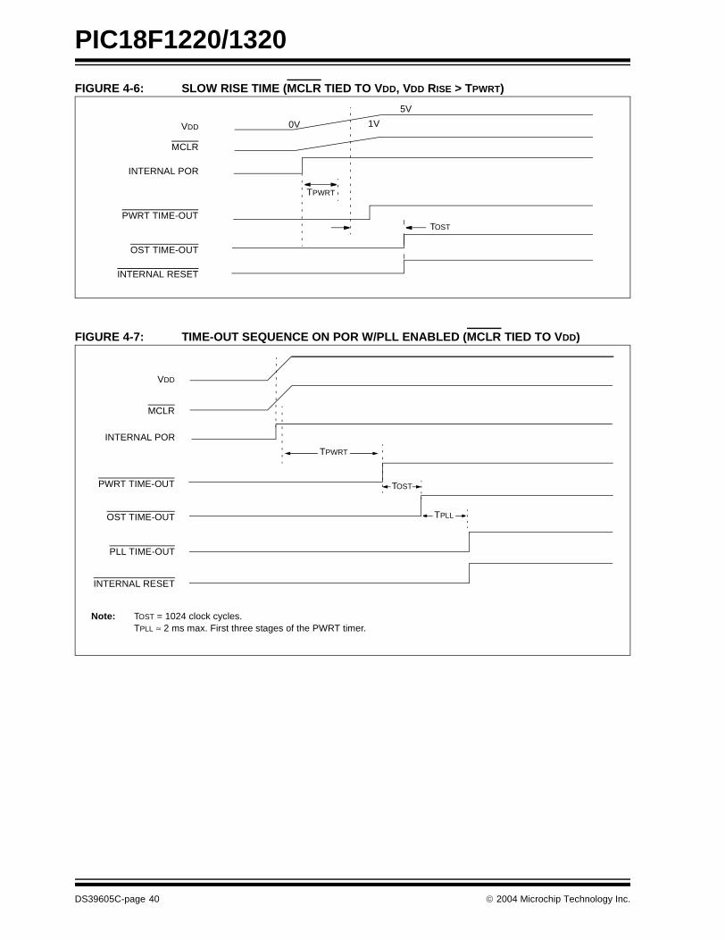
PIC18F1220/1320
FIGURE 4-6: SLOW RISE TIME (MCLR TIED TO VDD, VDD RISE > TPWRT)
FIGURE 4-7: TIME-OUT SEQUENCE ON POR W/PLL ENABLED (MCLR TIED TO VDD)
VDD
MCLR
INTERNAL POR
PWRT TIME-OUT
OST TIME-OUT
INTERNAL RESET
0V 1V
5V
TPWRT
TOST
TPWRT
TOST
VDD
MCLR
INTERNAL POR
PWRT TIME-OUT
OST TIME-OUT
INTERNAL RESET
PLL TIME-OUT
TPLL
Note: TOST = 1024 clock cycles.TPLL ≈ 2 ms max. First three stages of the PWRT timer.
DS39605C-page 40 2004 Microchip Technology Inc.

PIC18F1220/1320
5.0 MEMORY ORGANIZATION
There are three memory types in Enhanced MCUdevices. These memory types are:
• Program Memory
• Data RAM • Data EEPROM
Data and program memory use separate busses,which allows for concurrent access of these types.
Additional detailed information for Flash program mem-ory and data EEPROM is provided in Section 6.0“Flash Program Memory” and Section 7.0 “DataEEPROM Memory”, respectively.
FIGURE 5-1: PROGRAM MEMORY MAP AND STACK FOR PIC18F1220
5.1 Program Memory Organization
A 21-bit program counter is capable of addressing the2-Mbyte program memory space. Accessing a locationbetween the physically implemented memory and the2-Mbyte address will cause a read of all ‘0’s (a NOPinstruction).
The PIC18F1220 has 4 Kbytes of Flash memory andcan store up to 2,048 single-word instructions.
The PIC18F1320 has 8 Kbytes of Flash memory andcan store up to 4,096 single-word instructions.
The Reset vector address is at 0000h and the interruptvector addresses are at 0008h and 0018h.
The program memory maps for the PIC18F1220 andPIC18F1320 devices are shown in Figure 5-1 andFigure 5-2, respectively.
FIGURE 5-2: PROGRAM MEMORY MAP AND STACK FOR PIC18F1320
PC<20:0>
Stack Level 1•
Stack Level 31
Reset Vector
Low Priority Interrupt Vector
••
CALL,RCALL,RETURNRETFIE,RETLW
21
0000h
0018h
On-ChipProgram Memory
High Priority Interrupt Vector 0008h
Use
r M
emor
y S
pace
1FFFFFh
1000h0FFFh
Read ‘0’
200000h
PC<20:0>
Stack Level 1•
Stack Level 31
Reset Vector
Low Priority Interrupt Vector
••
CALL,RCALL,RETURNRETFIE,RETLW
21
0000h
0018h
2000h
1FFFh
On-ChipProgram Memory
High Priority Interrupt Vector 0008h
Use
r M
emor
y S
pace
Read ‘0’
1FFFFFh200000h
2004 Microchip Technology Inc. DS39605C-page 41
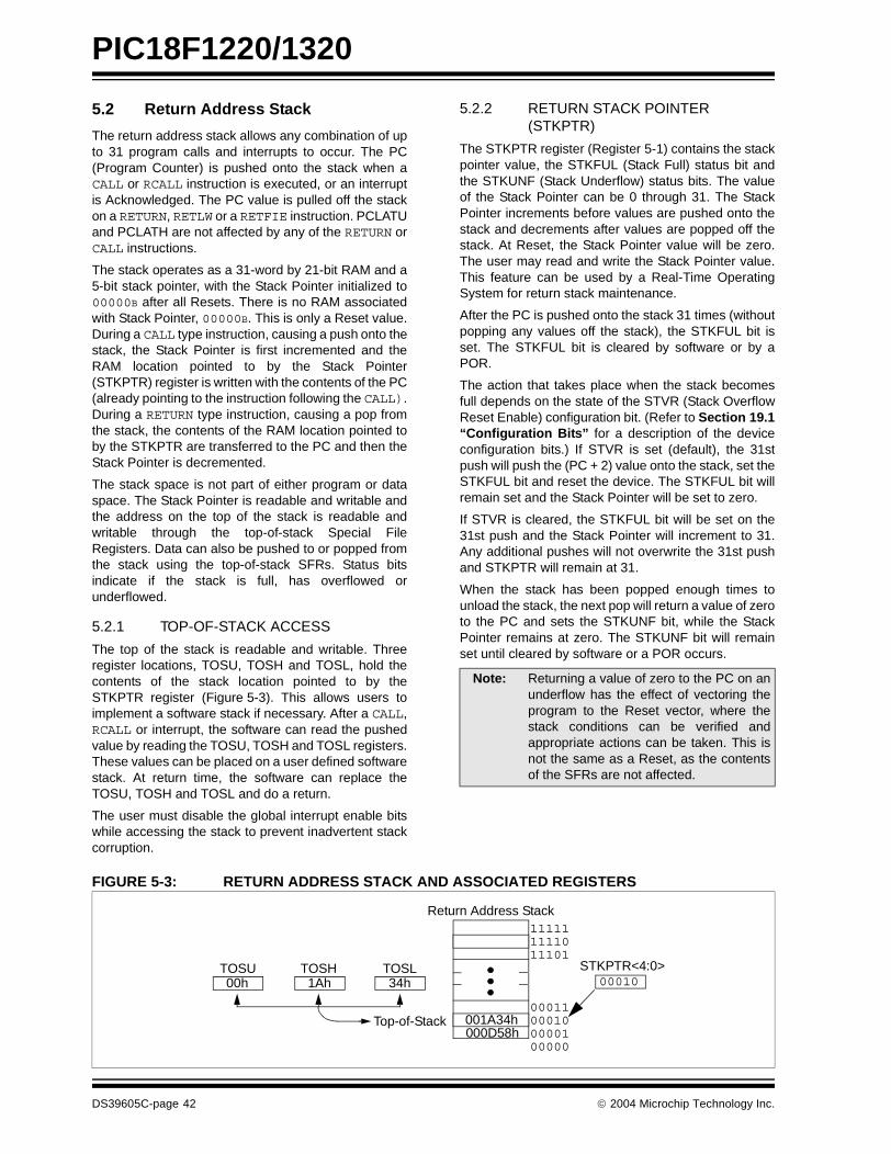
PIC18F1220/1320
5.2 Return Address Stack
The return address stack allows any combination of upto 31 program calls and interrupts to occur. The PC(Program Counter) is pushed onto the stack when aCALL or RCALL instruction is executed, or an interruptis Acknowledged. The PC value is pulled off the stackon a RETURN, RETLW or a RETFIE instruction. PCLATUand PCLATH are not affected by any of the RETURN orCALL instructions.
The stack operates as a 31-word by 21-bit RAM and a5-bit stack pointer, with the Stack Pointer initialized to00000B after all Resets. There is no RAM associatedwith Stack Pointer, 00000B. This is only a Reset value.During a CALL type instruction, causing a push onto thestack, the Stack Pointer is first incremented and theRAM location pointed to by the Stack Pointer(STKPTR) register is written with the contents of the PC(already pointing to the instruction following the CALL).During a RETURN type instruction, causing a pop fromthe stack, the contents of the RAM location pointed toby the STKPTR are transferred to the PC and then theStack Pointer is decremented.
The stack space is not part of either program or dataspace. The Stack Pointer is readable and writable andthe address on the top of the stack is readable andwritable through the top-of-stack Special FileRegisters. Data can also be pushed to or popped fromthe stack using the top-of-stack SFRs. Status bitsindicate if the stack is full, has overflowed orunderflowed.
5.2.1 TOP-OF-STACK ACCESS
The top of the stack is readable and writable. Threeregister locations, TOSU, TOSH and TOSL, hold thecontents of the stack location pointed to by theSTKPTR register (Figure 5-3). This allows users toimplement a software stack if necessary. After a CALL,RCALL or interrupt, the software can read the pushedvalue by reading the TOSU, TOSH and TOSL registers.These values can be placed on a user defined softwarestack. At return time, the software can replace theTOSU, TOSH and TOSL and do a return.
The user must disable the global interrupt enable bitswhile accessing the stack to prevent inadvertent stackcorruption.
5.2.2 RETURN STACK POINTER (STKPTR)
The STKPTR register (Register 5-1) contains the stackpointer value, the STKFUL (Stack Full) status bit andthe STKUNF (Stack Underflow) status bits. The valueof the Stack Pointer can be 0 through 31. The StackPointer increments before values are pushed onto thestack and decrements after values are popped off thestack. At Reset, the Stack Pointer value will be zero.The user may read and write the Stack Pointer value.This feature can be used by a Real-Time OperatingSystem for return stack maintenance.
After the PC is pushed onto the stack 31 times (withoutpopping any values off the stack), the STKFUL bit isset. The STKFUL bit is cleared by software or by aPOR.
The action that takes place when the stack becomesfull depends on the state of the STVR (Stack OverflowReset Enable) configuration bit. (Refer to Section 19.1“Configuration Bits” for a description of the deviceconfiguration bits.) If STVR is set (default), the 31stpush will push the (PC + 2) value onto the stack, set theSTKFUL bit and reset the device. The STKFUL bit willremain set and the Stack Pointer will be set to zero.
If STVR is cleared, the STKFUL bit will be set on the31st push and the Stack Pointer will increment to 31.Any additional pushes will not overwrite the 31st pushand STKPTR will remain at 31.
When the stack has been popped enough times tounload the stack, the next pop will return a value of zeroto the PC and sets the STKUNF bit, while the StackPointer remains at zero. The STKUNF bit will remainset until cleared by software or a POR occurs.
FIGURE 5-3: RETURN ADDRESS STACK AND ASSOCIATED REGISTERS
Note: Returning a value of zero to the PC on anunderflow has the effect of vectoring theprogram to the Reset vector, where thestack conditions can be verified andappropriate actions can be taken. This isnot the same as a Reset, as the contentsof the SFRs are not affected.
00011001A34h
111111111011101
000100000100000
00010
Return Address Stack
Top-of-Stack000D58h
TOSLTOSHTOSU34h1Ah00h
STKPTR<4:0>
DS39605C-page 42 2004 Microchip Technology Inc.
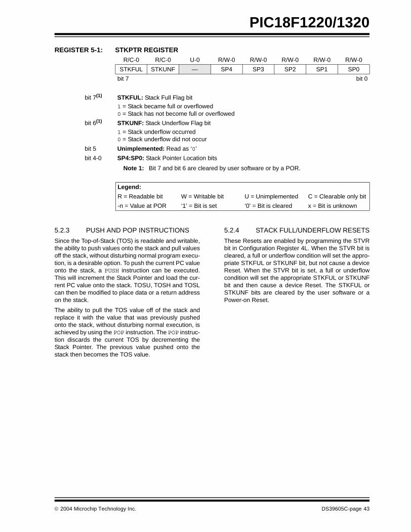
PIC18F1220/1320
REGISTER 5-1: STKPTR REGISTER
5.2.3 PUSH AND POP INSTRUCTIONS
Since the Top-of-Stack (TOS) is readable and writable,the ability to push values onto the stack and pull valuesoff the stack, without disturbing normal program execu-tion, is a desirable option. To push the current PC valueonto the stack, a PUSH instruction can be executed.This will increment the Stack Pointer and load the cur-rent PC value onto the stack. TOSU, TOSH and TOSLcan then be modified to place data or a return addresson the stack.
The ability to pull the TOS value off of the stack andreplace it with the value that was previously pushedonto the stack, without disturbing normal execution, isachieved by using the POP instruction. The POP instruc-tion discards the current TOS by decrementing theStack Pointer. The previous value pushed onto thestack then becomes the TOS value.
5.2.4 STACK FULL/UNDERFLOW RESETS
These Resets are enabled by programming the STVRbit in Configuration Register 4L. When the STVR bit iscleared, a full or underflow condition will set the appro-priate STKFUL or STKUNF bit, but not cause a deviceReset. When the STVR bit is set, a full or underflowcondition will set the appropriate STKFUL or STKUNFbit and then cause a device Reset. The STKFUL orSTKUNF bits are cleared by the user software or aPower-on Reset.
R/C-0 R/C-0 U-0 R/W-0 R/W-0 R/W-0 R/W-0 R/W-0
STKFUL STKUNF — SP4 SP3 SP2 SP1 SP0
bit 7 bit 0
bit 7(1) STKFUL: Stack Full Flag bit1 = Stack became full or overflowed 0 = Stack has not become full or overflowed
bit 6(1) STKUNF: Stack Underflow Flag bit
1 = Stack underflow occurred 0 = Stack underflow did not occur
bit 5 Unimplemented: Read as ‘0’
bit 4-0 SP4:SP0: Stack Pointer Location bits
Note 1: Bit 7 and bit 6 are cleared by user software or by a POR.
Legend:
R = Readable bit W = Writable bit U = Unimplemented C = Clearable only bit
-n = Value at POR ‘1’ = Bit is set ‘0’ = Bit is cleared x = Bit is unknown
2004 Microchip Technology Inc. DS39605C-page 43
PIC18F1220/1320
5.3 Fast Register Stack
A “fast return” option is available for interrupts. A fastregister stack is provided for the Status, WREG andBSR registers and is only one in depth. The stack is notreadable or writable and is loaded with the currentvalue of the corresponding register when the processorvectors for an interrupt. The values in the registers arethen loaded back into the working registers, if theRETFIE, FAST instruction is used to return from theinterrupt.
All interrupt sources will push values into the stackregisters. If both low and high priority interrupts areenabled, the stack registers cannot be used reliably toreturn from low priority interrupts. If a high priority inter-rupt occurs while servicing a low priority interrupt, thestack register values stored by the low priority interruptwill be overwritten. Users must save the key registersin software during a low priority interrupt.
If interrupt priority is not used, all interrupts may use thefast register stack for returns from interrupt.
If no interrupts are used, the fast register stack can beused to restore the Status, WREG and BSR registers atthe end of a subroutine call. To use the fast registerstack for a subroutine call, a CALL LABEL, FASTinstruction must be executed to save the Status,WREG and BSR registers to the fast register stack. ARETURN, FAST instruction is then executed to restorethese registers from the fast register stack.
Example 5-1 shows a source code example that usesthe fast register stack during a subroutine call andreturn.
EXAMPLE 5-1: FAST REGISTER STACK CODE EXAMPLE
5.4 PCL, PCLATH and PCLATU
The Program Counter (PC) specifies the address of theinstruction to fetch for execution. The PC is 21-bitswide. The low byte, known as the PCL register, is bothreadable and writable. The high byte, or PCH register,contains the PC<15:8> bits and is not directly readableor writable. Updates to the PCH register may be per-formed through the PCLATH register. The upper byte iscalled PCU. This register contains the PC<20:16> bitsand is not directly readable or writable. Updates to thePCU register may be performed through the PCLATUregister.
The contents of PCLATH and PCLATU will betransferred to the program counter by any operationthat writes PCL. Similarly, the upper two bytes of theprogram counter will be transferred to PCLATH andPCLATU by an operation that reads PCL. This is usefulfor computed offsets to the PC (see Section 5.8.1“Computed GOTO”).
The PC addresses bytes in the program memory. Toprevent the PC from becoming misaligned with wordinstructions, the LSB of PCL is fixed to a value of ‘0’.The PC increments by 2 to address sequentialinstructions in the program memory.
The CALL, RCALL, GOTO and program branch instruc-tions write to the program counter directly. For theseinstructions, the contents of PCLATH and PCLATU arenot transferred to the program counter.
CALL SUB1, FAST ;STATUS, WREG, BSR;SAVED IN FAST REGISTER;STACK
••
SUB1 ••
RETURN, FAST ;RESTORE VALUES SAVED;IN FAST REGISTER STACK
DS39605C-page 44 2004 Microchip Technology Inc.

PIC18F1220/1320
5.5 Clocking Scheme/Instruction Cycle
The clock input (from OSC1) is internally divided byfour to generate four non-overlapping quadratureclocks, namely Q1, Q2, Q3 and Q4. Internally, theProgram Counter (PC) is incremented every Q1, theinstruction is fetched from the program memory andlatched into the instruction register in Q4. The instruc-tion is decoded and executed during the following Q1through Q4. The clocks and instruction execution floware shown in Figure 5-4.
5.6 Instruction Flow/Pipelining
An “Instruction Cycle” consists of four Q cycles (Q1,Q2, Q3 and Q4). The instruction fetch and execute arepipelined such that fetch takes one instruction cycle,while decode and execute takes another instructioncycle. However, due to the pipelining, each instructioneffectively executes in one cycle. If an instructioncauses the program counter to change (e.g., GOTO),then two cycles are required to complete the instruction(Example 5-2).
A fetch cycle begins with the Program Counter (PC)incrementing in Q1.
In the execution cycle, the fetched instruction is latchedinto the “Instruction Register” (IR) in cycle Q1. Thisinstruction is then decoded and executed during theQ2, Q3 and Q4 cycles. Data memory is read during Q2(operand read) and written during Q4 (destinationwrite).
FIGURE 5-4: CLOCK/INSTRUCTION CYCLE
EXAMPLE 5-2: INSTRUCTION PIPELINE FLOW
Q1 Q2 Q3 Q4 Q1 Q2 Q3 Q4 Q1 Q2 Q3 Q4
OSC1
Q1
Q2
Q3
Q4
PC
OSC2/CLKO(RC Mode)
PC PC + 2 PC + 4
Fetch INST (PC)Execute INST (PC – 2)
Fetch INST (PC + 2)Execute INST (PC)
Fetch INST (PC + 4)Execute INST (PC + 2)
InternalPhaseClock
All instructions are single cycle, except for any program branches. These take two cycles, since the fetch instructionis “flushed” from the pipeline, while the new instruction is being fetched and then executed.
TCY0 TCY1 TCY2 TCY3 TCY4 TCY5
1. MOVLW 55h Fetch 1 Execute 1
2. MOVWF PORTB Fetch 2 Execute 2
3. BRA SUB_1 Fetch 3 Execute 3
4. BSF PORTA, BIT3 (Forced NOP) Fetch 4 Flush (NOP)
5. Instruction @ address SUB_1 Fetch SUB_1 Execute SUB_1
2004 Microchip Technology Inc. DS39605C-page 45
PIC18F1220/1320
5.7 Instructions in Program Memory
The program memory is addressed in bytes. Instruc-tions are stored as two bytes or four bytes in programmemory. The Least Significant Byte of an instructionword is always stored in a program memory locationwith an even address (LSB = 0). Figure 5-5 shows anexample of how instruction words are stored in the pro-gram memory. To maintain alignment with instructionboundaries, the PC increments in steps of 2 and theLSB will always read ‘0’ (see Section 5.4 “PCL,PCLATH and PCLATU”).
The CALL and GOTO instructions have the absoluteprogram memory address embedded into the instruc-tion. Since instructions are always stored on wordboundaries, the data contained in the instruction is aword address. The word address is written toPC<20:1>, which accesses the desired byte address inprogram memory. Instruction #2 in Figure 5-5 showshow the instruction ‘GOTO 000006h’ is encoded in theprogram memory. Program branch instructions, whichencode a relative address offset, operate in the samemanner. The offset value stored in a branch instructionrepresents the number of single-word instructions thatthe PC will be offset by. Section 20.0 “Instruction SetSummary” provides further details of the instructionset.
FIGURE 5-5: INSTRUCTIONS IN PROGRAM MEMORY
5.7.1 TWO-WORD INSTRUCTIONS
PIC18F1220/1320 devices have four two-wordinstructions: MOVFF, CALL, GOTO and LFSR. The secondword of these instructions has the 4 MSBs set to ‘1’s andis decoded as a NOP instruction. The lower 12 bits of thesecond word contain data to be used by the instruction.If the first word of the instruction is executed, the data inthe second word is accessed. If the second word of the
instruction is executed by itself (first word was skipped),it will execute as a NOP. This action is necessary whenthe two-word instruction is preceded by a conditionalinstruction that results in a skip operation. A programexample that demonstrates this concept is shown inExample 5-3. Refer to Section 20.0 “Instruction SetSummary” for further details of the instruction set.
EXAMPLE 5-3: TWO-WORD INSTRUCTIONS
Word AddressLSB = 1 LSB = 0 ↓
Program MemoryByte Locations →
000000h000002h000004h000006h
Instruction 1: MOVLW 055h 0Fh 55h 000008hInstruction 2: GOTO 000006h EFh 03h 00000Ah
F0h 00h 00000ChInstruction 3: MOVFF 123h, 456h C1h 23h 00000Eh
F4h 56h 000010h000012h000014h
CASE 1:
Object Code Source Code
0110 0110 0000 0000 TSTFSZ REG1 ; is RAM location 0?
1100 0001 0010 0011 MOVFF REG1, REG2 ; No, skip this word
1111 0100 0101 0110 ; Execute this word as a NOP
0010 0100 0000 0000 ADDWF REG3 ; continue code
CASE 2:
Object Code Source Code
0110 0110 0000 0000 TSTFSZ REG1 ; is RAM location 0?
1100 0001 0010 0011 MOVFF REG1, REG2 ; Yes, execute this word
1111 0100 0101 0110 ; 2nd word of instruction
0010 0100 0000 0000 ADDWF REG3 ; continue code
DS39605C-page 46 2004 Microchip Technology Inc.

PIC18F1220/1320
5.8 Look-up Tables
Look-up tables are implemented two ways:
• Computed GOTO
• Table Reads
5.8.1 COMPUTED GOTO
A computed GOTO is accomplished by adding an offsetto the program counter (see Example 5-4).
A look-up table can be formed with an ADDWF PCLinstruction and a group of RETLW 0xnn instructions.WREG is loaded with an offset into the table beforeexecuting a call to that table. The first instruction of thecalled routine is the ADDWF PCL instruction. The nextinstruction executed will be one of the RETLW 0xnninstructions, that returns the value 0xnn to the callingfunction.
The offset value (in WREG) specifies the number ofbytes that the program counter should advance andshould be multiples of 2 (LSB = 0).
In this method, only one data byte may be stored ineach instruction location and room on the returnaddress stack is required.
EXAMPLE 5-4: COMPUTED GOTO USING AN OFFSET VALUE
5.8.2 TABLE READS/TABLE WRITES
A better method of storing data in program memoryallows two bytes of data to be stored in each instructionlocation.
Look-up table data may be stored two bytes per pro-gram word by using table reads and writes. The TablePointer (TBLPTR) register specifies the byte addressand the Table Latch (TABLAT) register contains thedata that is read from or written to program memory.Data is transferred to/from program memory, one byteat a time.
The table read/table write operation is discussedfurther in Section 6.1 “Table Reads and TableWrites”.
5.9 Data Memory Organization
The data memory is implemented as static RAM. Eachregister in the data memory has a 12-bit address,allowing up to 4096 bytes of data memory. Figure 5-6shows the data memory organization for thePIC18F1220/1320 devices.
The data memory map is divided into as many as16 banks that contain 256 bytes each. The lower 4 bitsof the Bank Select Register (BSR<3:0>) select whichbank will be accessed. The upper 4 bits for the BSR arenot implemented.
The data memory contains Special Function Registers(SFR) and General Purpose Registers (GPR). TheSFRs are used for control and status of the controllerand peripheral functions, while GPRs are used for datastorage and scratch pad operations in the user’s appli-cation. The SFRs start at the last location of Bank 15(FFFh) and extend towards F80h. Any remaining spacebeyond the SFRs in the Bank may be implemented asGPRs. GPRs start at the first location of Bank 0 andgrow upwards. Any read of an unimplemented locationwill read as ‘0’s.
The entire data memory may be accessed directly orindirectly. Direct addressing may require the use of theBSR register. Indirect addressing requires the use of aFile Select Register (FSRn) and a corresponding Indi-rect File Operand (INDFn). Each FSR holds a 12-bitaddress value that can be used to access any locationin the Data Memory map without banking. SeeSection 5.12 “Indirect Addressing, INDF and FSRRegisters” for indirect addressing details.
The instruction set and architecture allow operationsacross all banks. This may be accomplished by indirectaddressing or by the use of the MOVFF instruction. TheMOVFF instruction is a two-word/two-cycle instructionthat moves a value from one register to another.
To ensure that commonly used registers (SFRs andselect GPRs) can be accessed in a single cycle,regardless of the current BSR values, an Access Bankis implemented. A segment of Bank 0 and a segment ofBank 15 comprise the Access RAM. Section 5.10“Access Bank” provides a detailed description of theAccess RAM.
5.9.1 GENERAL PURPOSE REGISTER FILE
Enhanced MCU devices may have banked memory inthe GPR area. GPRs are not initialized by a Power-onReset and are unchanged on all other Resets.
Data RAM is available for use as GPR registers by allinstructions. The second half of Bank 15 (F80h toFFFh) contains SFRs. All other banks of data memorycontain GPRs, starting with Bank 0.
MOVFW OFFSETCALL TABLE
ORG 0xnn00TABLE ADDWF PCL
RETLW 0xnnRETLW 0xnnRETLW 0xnn...
2004 Microchip Technology Inc. DS39605C-page 47

PIC18F1220/1320
FIGURE 5-6: DATA MEMORY MAP FOR PIC18F1220/1320 DEVICES
Bank 0
Bank 14
Bank 15
Data Memory MapBSR<3:0>
= 0000
= 1111
080h07Fh
F80hFFFh
00h
7Fh80h
FFh
Access Bank
When a = 0,
The BSR is ignored and theAccess Bank is used.
The first 128 bytes are General Purpose RAM (from Bank 0).
The second 128 bytes areSpecial Function Registers(from Bank 15).
When a = 1,
The BSR specifies the Bankused by the instruction.
F7FhF00hEFFh
0FFh
000hAccess RAM
FFh
00h
FFh
00h
GPR
SFR
Unused
Access RAM High
Access RAM Low
Bank 1to
UnusedRead ‘00h’= 1110
= 0001
(SFRs)
DS39605C-page 48 2004 Microchip Technology Inc.

PIC18F1220/1320
5.9.2 SPECIAL FUNCTION REGISTERS
The Special Function Registers (SFRs) are registersused by the CPU and peripheral modules for controllingthe desired operation of the device. These registers areimplemented as static RAM. A list of these registers isgiven in Table 5-1 and Table 5-2.
The SFRs can be classified into two sets: those asso-ciated with the “core” function and those related to theperipheral functions. Those registers related to the“core” are described in this section, while those relatedto the operation of the peripheral features aredescribed in the section of that peripheral feature.
The SFRs are typically distributed among the peripheralswhose functions they control.
The unused SFR locations will be unimplemented andread as ‘0’s.
TABLE 5-1: SPECIAL FUNCTION REGISTER MAP FOR PIC18F1220/1320 DEVICES Address Name Address Name Address Name Address Name
FFFh TOSU FDFh INDF2(2) FBFh CCPR1H F9Fh IPR1
FFEh TOSH FDEh POSTINC2(2) FBEh CCPR1L F9Eh PIR1
FFDh TOSL FDDh POSTDEC2(2) FBDh CCP1CON F9Dh PIE1
FFCh STKPTR FDCh PREINC2(2) FBCh — F9Ch —
FFBh PCLATU FDBh PLUSW2(2) FBBh — F9Bh OSCTUNE
FFAh PCLATH FDAh FSR2H FBAh — F9Ah —
FF9h PCL FD9h FSR2L FB9h — F99h —
FF8h TBLPTRU FD8h STATUS FB8h — F98h —
FF7h TBLPTRH FD7h TMR0H FB7h PWM1CON F97h —
FF6h TBLPTRL FD6h TMR0L FB6h ECCPAS F96h —
FF5h TABLAT FD5h T0CON FB5h — F95h —
FF4h PRODH FD4h — FB4h — F94h —
FF3h PRODL FD3h OSCCON FB3h TMR3H F93h TRISB
FF2h INTCON FD2h LVDCON FB2h TMR3L F92h TRISA
FF1h INTCON2 FD1h WDTCON FB1h T3CON F91h —
FF0h INTCON3 FD0h RCON FB0h SPBRGH F90h —
FEFh INDF0(2) FCFh TMR1H FAFh SPBRG F8Fh —
FEEh POSTINC0(2) FCEh TMR1L FAEh RCREG F8Eh —
FEDh POSTDEC0(2) FCDh T1CON FADh TXREG F8Dh —
FECh PREINC0(2) FCCh TMR2 FACh TXSTA F8Ch —
FEBh PLUSW0(2) FCBh PR2 FABh RCSTA F8Bh —
FEAh FSR0H FCAh T2CON FAAh BAUDCTL F8Ah LATB
FE9h FSR0L FC9h — FA9h EEADR F89h LATA
FE8h WREG FC8h — FA8h EEDATA F88h —
FE7h INDF1(2) FC7h — FA7h EECON2 F87h —
FE6h POSTINC1(2) FC6h — FA6h EECON1 F86h —
FE5h POSTDEC1(2) FC5h — FA5h — F85h —
FE4h PREINC1(2) FC4h ADRESH FA4h — F84h —
FE3h PLUSW1(2) FC3h ADRESL FA3h — F83h —
FE2h FSR1H FC2h ADCON0 FA2h IPR2 F82h —
FE1h FSR1L FC1h ADCON1 FA1h PIR2 F81h PORTB
FE0h BSR FC0h ADCON2 FA0h PIE2 F80h PORTA
Note 1: Unimplemented registers are read as ‘0’.2: This is not a physical register.
2004 Microchip Technology Inc. DS39605C-page 49
PIC18F1220/1320
TABLE 5-2: REGISTER FILE SUMMARY (PIC18F1220/1320)
File Name Bit 7 Bit 6 Bit 5 Bit 4 Bit 3 Bit 2 Bit 1 Bit 0 Value onPOR, BOR
Details on page:
TOSU — — — Top-of-Stack Upper Byte (TOS<20:16>) ---0 0000 36, 42
TOSH Top-of-Stack High Byte (TOS<15:8>) 0000 0000 36, 42
TOSL Top-of-Stack Low Byte (TOS<7:0>) 0000 0000 36, 42
STKPTR STKFUL STKUNF — Return Stack Pointer 00-0 0000 36, 43
PCLATU — — bit 21(3) Holding Register for PC<20:16> ---0 0000 36, 44
PCLATH Holding Register for PC<15:8> 0000 0000 36, 44
PCL PC Low Byte (PC<7:0>) 0000 0000 36, 44
TBLPTRU — — bit 21 Program Memory Table Pointer Upper Byte (TBLPTR<20:16>) --00 0000 36, 60
TBLPTRH Program Memory Table Pointer High Byte (TBLPTR<15:8>) 0000 0000 36, 60
TBLPTRL Program Memory Table Pointer Low Byte (TBLPTR<7:0>) 0000 0000 36, 60
TABLAT Program Memory Table Latch 0000 0000 36, 60
PRODH Product Register High Byte xxxx xxxx 36, 71
PRODL Product Register Low Byte xxxx xxxx 36, 71
INTCON GIE/GIEH PEIE/GIEL TMR0IE INT0IE RBIE TMR0IF INT0IF RBIF 0000 000x 36, 75
INTCON2 RBPU INTEDG0 INTEDG1 INTEDG2 — TMR0IP — RBIP 1111 -1-1 36, 76
INTCON3 INT2IP INT1IP — INT2IE INT1IE — INT2IF INT1IF 11-0 0-00 36, 77
INDF0 Uses contents of FSR0 to address data memory – value of FSR0 not changed (not a physical register) N/A 36, 53
POSTINC0 Uses contents of FSR0 to address data memory – value of FSR0 post-incremented (not a physical register) N/A 36, 53
POSTDEC0 Uses contents of FSR0 to address data memory– value of FSR0 post-decremented (not a physical register) N/A 36, 53
PREINC0 Uses contents of FSR0 to address data memory – value of FSR0 pre-incremented (not a physical register) N/A 36, 53
PLUSW0 Uses contents of FSR0 to address data memory – value of FSR0 offset by W (not a physical register) N/A 36, 53
FSR0H — — — — Indirect Data Memory Address Pointer 0 High ---- 0000 36, 53
FSR0L Indirect Data Memory Address Pointer 0 Low Byte xxxx xxxx 36, 53
WREG Working Register xxxx xxxx 36
INDF1 Uses contents of FSR1 to address data memory – value of FSR1 not changed (not a physical register) N/A 36, 53
POSTINC1 Uses contents of FSR1 to address data memory – value of FSR1 post-incremented (not a physical register) N/A 36, 53
POSTDEC1 Uses contents of FSR1 to address data memory – value of FSR1 post-decremented (not a physical register) N/A 36, 53
PREINC1 Uses contents of FSR1 to address data memory – value of FSR1 pre-incremented (not a physical register) N/A 36, 53
PLUSW1 Uses contents of FSR1 to address data memory – value of FSR1 offset by W (not a physical register) N/A 36, 53
FSR1H — — — — Indirect Data Memory Address Pointer 1 High ---- 0000 36, 53
FSR1L Indirect Data Memory Address Pointer 1 Low Byte xxxx xxxx 36, 53
BSR — — — — Bank Select Register ---- 0000 37, 52
INDF2 Uses contents of FSR2 to address data memory – value of FSR2 not changed (not a physical register) N/A 37, 53
POSTINC2 Uses contents of FSR2 to address data memory – value of FSR2 post-incremented (not a physical register) N/A 37, 53
POSTDEC2 Uses contents of FSR2 to address data memory – value of FSR2 post-decremented (not a physical register) N/A 37, 53
PREINC2 Uses contents of FSR2 to address data memory – value of FSR2 pre-incremented (not a physical register) N/A 37, 53
PLUSW2 Uses contents of FSR2 to address data memory – value of FSR2 offset by W (not a physical register) N/A 37, 53
FSR2H — — — — Indirect Data Memory Address Pointer 2 High ---- 0000 37, 53
FSR2L Indirect Data Memory Address Pointer 2 Low Byte xxxx xxxx 37, 53
STATUS — — — N OV Z DC C ---x xxxx 37, 55
TMR0H Timer0 Register High Byte 0000 0000 37, 101
TMR0L Timer0 Register Low Byte xxxx xxxx 37, 101
T0CON TMR0ON T08BIT T0CS T0SE PSA T0PS2 T0PS1 T0PS0 1111 1111 37, 99
OSCCON IDLEN IRCF2 IRCF1 IRCF0 OSTS IOFS SCS1 SCS0 0000 q000 37, 17
LVDCON — — IVRST LVDEN LVDL3 LVDL2 LVDL1 LVDL0 --00 0101 37, 167
WDTCON — — — — — — — SWDTEN --- ---0 37, 180
RCON IPEN — — RI TO PD POR BOR 0--1 11q0 35, 56, 84
Legend: x = unknown, u = unchanged, – = unimplemented, q = value depends on conditionNote 1: RA6 and associated bits are configured as port pins in RCIO, ECIO and INTIO2 (with port function on RA6) Oscillator mode only and read ‘0’
in all other oscillator modes.2: RA7 and associated bits are configured as port pins in INTIO2 Oscillator mode only and read ‘0’ in all other modes.3: Bit 21 of the PC is only available in Test mode and Serial Programming modes.4: The RA5 port bit is only available when MCLRE fuse (CONFIG3H<7>) is programmed to ‘0’. Otherwise, RA5 reads ‘0’. This bit is read-only.
DS39605C-page 50 2004 Microchip Technology Inc.
PIC18F1220/1320
TMR1H Timer1 Register High Byte xxxx xxxx 37, 108
TMR1L Timer1 Register Low Byte xxxx xxxx 37, 108
T1CON RD16 T1RUN T1CKPS1 T1CKPS0 T1OSCEN T1SYNC TMR1CS TMR1ON 0000 0000 37, 103
TMR2 Timer2 Register 0000 0000 37, 109
PR2 Timer2 Period Register 1111 1111 37, 109
T2CON — TOUTPS3 TOUTPS2 TOUTPS1 TOUTPS0 TMR2ON T2CKPS1 T2CKPS0 -000 0000 37, 109
ADRESH A/D Result Register High Byte xxxx xxxx 37, 164
ADRESL A/D Result Register Low Byte xxxx xxxx 37, 164
ADCON0 VCFG1 VCFG0 — CHS2 CHS1 CHS0 GO/DONE ADON 00-0 0000 37, 155
ADCON1 — PCFG6 PCFG5 PCFG4 PCFG3 PCFG2 PCFG1 PCFG0 -000 0000 37, 156
ADCON2 ADFM — ACQT2 ACQT1 ACQT0 ADCS2 ADCS1 ADCS0 0-00 0000 37, 157
CCPR1H Capture/Compare/PWM Register 1 High Byte xxxx xxxx 37. 116
CCPR1L Capture/Compare/PWM Register 1 Low Byte xxxx xxxx 37, 116
CCP1CON P1M1 P1M0 DC1B1 DC1B0 CCP1M3 CCP1M2 CCP1M1 CCP1M0 0000 0000 37, 115
PWM1CON PRSEN PDC6 PDC5 PDC4 PDC3 PDC2 PDC1 PDC0 0000 0000 37, 126
ECCPAS ECCPASE ECCPAS2 ECCPAS1 ECCPAS0 PSSAC1 PSSAC0 PSSBD1 PSSBD0 0000 0000 37, 127
TMR3H Timer3 Register High Byte xxxx xxxx 38, 113
TMR3L Timer3 Register Low Byte xxxx xxxx 38, 113
T3CON RD16 — T3CKPS1 T3CKPS0 T3CCP1 T3SYNC TMR3CS TMR3ON 0-00 0000 38, 111
SPBRGH EUSART Baud Rate Generator High Byte 0000 0000 38
SPBRG EUSART Baud Rate Generator Low Byte 0000 0000 38, 135
RCREG EUSART Receive Register 0000 0000 38, 143, 142
TXREG EUSART Transmit Register 0000 0000 38, 140, 142
TXSTA CSRC TX9 TXEN SYNC SENDB BRGH TRMT TX9D 0000 0010 38, 132
RCSTA SPEN RX9 SREN CREN ADDEN FERR OERR RX9D 0000 000x 38, 133
BAUDCTL — RCIDL — SCKP BRG16 — WUE ABDEN -1-1 0-00 38
EEADR EEPROM Address Register 0000 0000 38, 67
EEDATA EEPROM Data Register 0000 0000 38, 70
EECON2 EEPROM Control Register 2 (not a physical register) 0000 0000 38, 58, 67
EECON1 EEPGD CFGS — FREE WRERR WREN WR RD xx-0 x000 38, 59, 68
IPR2 OSCFIP — — EEIP — LVDIP TMR3IP — 1--1 -11- 38, 83
PIR2 OSCFIF — — EEIF — LVDIF TMR3IF — 0--0 -00- 38, 79
PIE2 OSCFIE — — EEIE — LVDIE TMR3IE — 0--0 -00- 38, 81
IPR1 — ADIP RCIP TXIP — CCP1IP TMR2IP TMR1IP -111 -111 38, 82
PIR1 — ADIF RCIF TXIF — CCP1IF TMR2IF TMR1IF -000 -000 38, 78
PIE1 — ADIE RCIE TXIE — CCP1IE TMR2IE TMR1IE -000 -000 38, 80
OSCTUNE — — TUN5 TUN4 TUN3 TUN2 TUN1 TUN0 --00 0000 38, 15
TRISB Data Direction Control Register for PORTB 1111 1111 38, 98
TRISA TRISA7(2) TRISA6(1) — Data Direction Control Register for PORTA 11-1 1111 38, 89
LATB Read/Write PORTB Data Latch xxxx xxxx 38, 98
LATA LATA<7>(2) LATA<6>(1) — Read/Write PORTA Data Latch xx-x xxxx 38, 89
PORTB Read PORTB pins, Write PORTB Data Latch xxxx xxxx 38, 98
PORTA RA7(2) RA6(1) RA5(4) Read PORTA pins, Write PORTA Data Latch xx0x 0000 38, 89
TABLE 5-2: REGISTER FILE SUMMARY (PIC18F1220/1320) (CONTINUED)
File Name Bit 7 Bit 6 Bit 5 Bit 4 Bit 3 Bit 2 Bit 1 Bit 0 Value onPOR, BOR
Details on page:
Legend: x = unknown, u = unchanged, – = unimplemented, q = value depends on conditionNote 1: RA6 and associated bits are configured as port pins in RCIO, ECIO and INTIO2 (with port function on RA6) Oscillator mode only and read ‘0’
in all other oscillator modes.2: RA7 and associated bits are configured as port pins in INTIO2 Oscillator mode only and read ‘0’ in all other modes.3: Bit 21 of the PC is only available in Test mode and Serial Programming modes.4: The RA5 port bit is only available when MCLRE fuse (CONFIG3H<7>) is programmed to ‘0’. Otherwise, RA5 reads ‘0’. This bit is read-only.
2004 Microchip Technology Inc. DS39605C-page 51

PIC18F1220/1320
5.10 Access Bank
The Access Bank is an architectural enhancementwhich is very useful for C compiler code optimization.The techniques used by the C compiler may also beuseful for programs written in assembly.
This data memory region can be used for:
• Intermediate computational values
• Local variables of subroutines• Faster context saving/switching of variables• Common variables
• Faster evaluation/control of SFRs (no banking)
The Access Bank is comprised of the last 128 bytes inBank 15 (SFRs) and the first 128 bytes in Bank 0.These two sections will be referred to as Access RAMHigh and Access RAM Low, respectively. Figure 5-6indicates the Access RAM areas.
A bit in the instruction word specifies if the operation isto occur in the bank specified by the BSR register or inthe Access Bank. This bit is denoted as the ‘a’ bit (foraccess bit).
When forced in the Access Bank (a = 0), the lastaddress in Access RAM Low is followed by the firstaddress in Access RAM High. Access RAM High mapsthe Special Function Registers, so these registers canbe accessed without any software overhead. This isuseful for testing status flags and modifying control bits.
5.11 Bank Select Register (BSR)
The need for a large general purpose memory spacedictates a RAM banking scheme. The data memory ispartitioned into as many as sixteen banks. When usingdirect addressing, the BSR should be configured for thedesired bank.
BSR<3:0> holds the upper 4 bits of the 12-bit RAMaddress. The BSR<7:4> bits will always read ‘0’s andwrites will have no effect (see Figure 5-7).
A MOVLB instruction has been provided in the instructionset to assist in selecting banks.
If the currently selected bank is not implemented, anyread will return all ‘0’s and all writes are ignored. TheStatus register bits will be set/cleared as appropriate forthe instruction performed.
Each Bank extends up to FFh (256 bytes). All datamemory is implemented as static RAM.
A MOVFF instruction ignores the BSR, since the 12-bitaddresses are embedded into the instruction word.
Section 5.12 “Indirect Addressing, INDF and FSRRegisters” provides a description of indirect address-ing, which allows linear addressing of the entire RAMspace.
FIGURE 5-7: DIRECT ADDRESSING
Note 1: For register file map detail, see Table 5-1.2: The access bit of the instruction can be used to force an override of the selected bank (BSR<3:0>) to the registers
of the Access Bank.3: The MOVFF instruction embeds the entire 12-bit address in the instruction.
DataMemory(1)
Direct Addressing
Bank Select(2) Location Select(3)
BSR<3:0> 7 0From Opcode(3)
00h 01h 0Eh 0Fh
Bank 0 Bank 1 Bank 14 Bank 15
1FFh
100h
0FFh
000h
EFFh
E00h
FFFh
F00h
BSR<7:4>
0 0 0 0
DS39605C-page 52 2004 Microchip Technology Inc.
PIC18F1220/1320
5.12 Indirect Addressing, INDF and FSR Registers
Indirect addressing is a mode of addressing data mem-ory, where the data memory address in the instructionis not fixed. An FSR register is used as a pointer to thedata memory location that is to be read or written. Sincethis pointer is in RAM, the contents can be modified bythe program. This can be useful for data tables in thedata memory and for software stacks. Figure 5-8shows how the fetched instruction is modified prior tobeing executed.
Indirect addressing is possible by using one of theINDF registers. Any instruction, using the INDF regis-ter, actually accesses the register pointed to by the FileSelect Register, FSR. Reading the INDF register itself,indirectly (FSR = 0), will read 00h. Writing to the INDFregister indirectly, results in a no operation (NOP). TheFSR register contains a 12-bit address, which is shownin Figure 5-9.
The INDFn register is not a physical register. Address-ing INDFn actually addresses the register whoseaddress is contained in the FSRn register (FSRn is apointer). This is indirect addressing.
Example 5-5 shows a simple use of indirect addressingto clear the RAM in Bank 1 (locations 100h-1FFh) in aminimum number of instructions.
EXAMPLE 5-5: HOW TO CLEAR RAM (BANK 1) USING INDIRECT ADDRESSING
There are three indirect addressing registers. Toaddress the entire data memory space (4096 bytes),these registers are 12-bit wide. To store the 12 bits ofaddressing information, two 8-bit registers are required:
1. FSR0: composed of FSR0H:FSR0L
2. FSR1: composed of FSR1H:FSR1L3. FSR2: composed of FSR2H:FSR2L
In addition, there are registers INDF0, INDF1 andINDF2, which are not physically implemented. Readingor writing to these registers activates indirect address-ing, with the value in the corresponding FSR registerbeing the address of the data. If an instruction writes avalue to INDF0, the value will be written to the addresspointed to by FSR0H:FSR0L. A read from INDF1 readsthe data from the address pointed to byFSR1H:FSR1L. INDFn can be used in code anywherean operand can be used.
If INDF0, INDF1 or INDF2 are read indirectly via anFSR, all ‘0’s are read (zero bit is set). Similarly, ifINDF0, INDF1 or INDF2 are written to indirectly, theoperation will be equivalent to a NOP instruction and theStatus bits are not affected.
5.12.1 INDIRECT ADDRESSING OPERATION
Each FSR register has an INDF register associated withit, plus four additional register addresses. Performing anoperation using one of these five registers determineshow the FSR will be modified during indirect addressing.
When data access is performed using one of the fiveINDFn locations, the address selected will configurethe FSRn register to:
• Do nothing to FSRn after an indirect access (no change) – INDFn
• Auto-decrement FSRn after an indirect access (post-decrement) – POSTDECn
• Auto-increment FSRn after an indirect access (post-increment) – POSTINCn
• Auto-increment FSRn before an indirect access (pre-increment) – PREINCn
• Use the value in the WREG register as an offset to FSRn. Do not modify the value of the WREG or the FSRn register after an indirect access (no change) – PLUSWn
When using the auto-increment or auto-decrementfeatures, the effect on the FSR is not reflected in theStatus register. For example, if the indirect addresscauses the FSR to equal ‘0’, the Z bit will not be set.
Auto-incrementing or auto-decrementing an FSR affectsall 12 bits. That is, when FSRnL overflows from anincrement, FSRnH will be incremented automatically.
Adding these features allows the FSRn to be used as astack pointer, in addition to its uses for table operationsin data memory.
Each FSR has an address associated with it thatperforms an indexed indirect access. When a dataaccess to this INDFn location (PLUSWn) occurs, theFSRn is configured to add the signed value in theWREG register and the value in FSR to form theaddress before an indirect access. The FSR value isnot changed. The WREG offset range is -128 to +127.
If an FSR register contains a value that points to one ofthe INDFn, an indirect read will read 00h (zero bit isset), while an indirect write will be equivalent to a NOP(Status bits are not affected).
If an indirect addressing write is performed when the tar-get address is an FSRnH or FSRnL register, the data iswritten to the FSR register, but no pre- or post-increment/decrement is performed.
LFSR FSR0,0x100 ; NEXT CLRF POSTINC0 ; Clear INDF
; register then ; inc pointer
BTFSS FSR0H, 1 ; All done with; Bank1?
GOTO NEXT ; NO, clear next CONTINUE ; YES, continue
2004 Microchip Technology Inc. DS39605C-page 53

PIC18F1220/1320
FIGURE 5-8: INDIRECT ADDRESSING OPERATION
FIGURE 5-9: INDIRECT ADDRESSING
Opcode Address
File Address = Access of an Indirect Addressing Register
FSR
InstructionExecuted
InstructionFetched
RAM
Opcode File
1212
12
BSR<3:0>
84
0h
FFFh
Note 1: For register file map detail, see Table 5-1.
DataMemory(1)
Indirect AddressingFSRnH:FSRnL
3 0
0FFFh
0000h
Location Select
11 0
0 7
DS39605C-page 54 2004 Microchip Technology Inc.

PIC18F1220/1320
5.13 Status Register
The Status register, shown in Register 5-2, contains thearithmetic status of the ALU. As with any other SFR, itcan be the operand for any instruction.
If the Status register is the destination for an instructionthat affects the Z, DC, C, OV or N bits, the results of theinstruction are not written; instead, the status isupdated according to the instruction performed. There-fore, the result of an instruction with the Status registeras its destination may be different than intended. As anexample, CLRF STATUS will set the Z bit and leave theremaining Status bits unchanged (‘000u u1uu’).
It is recommended that only BCF, BSF, SWAPF, MOVFFand MOVWF instructions are used to alter the Status reg-ister, because these instructions do not affect the Z, C,DC, OV or N bits in the Status register.
For other instructions that do not affect Status bits, seethe instruction set summaries in Table 20-1.
REGISTER 5-2: STATUS REGISTER
Note: The C and DC bits operate as the borrowand digit borrow bits, respectively, insubtraction.
U-0 U-0 U-0 R/W-x R/W-x R/W-x R/W-x R/W-x
— — — N OV Z DC C
bit 7 bit 0
bit 7-5 Unimplemented: Read as ‘0’
bit 4 N: Negative bit This bit is used for signed arithmetic (2’s complement). It indicates whether the result was negative (ALU MSB = 1).1 = Result was negative 0 = Result was positive
bit 3 OV: Overflow bit This bit is used for signed arithmetic (2’s complement). It indicates an overflow of the 7-bit magnitude, which causes the sign bit (bit 7) to change state.1 = Overflow occurred for signed arithmetic (in this arithmetic operation) 0 = No overflow occurred
bit 2 Z: Zero bit
1 = The result of an arithmetic or logic operation is zero 0 = The result of an arithmetic or logic operation is not zero
bit 1 DC: Digit carry/borrow bit For ADDWF, ADDLW, SUBLW and SUBWF instructions: 1 = A carry-out from the 4th low-order bit of the result occurred 0 = No carry-out from the 4th low-order bit of the result
Note: For borrow, the polarity is reversed. A subtraction is executed by adding the2’s complement of the second operand. For rotate (RRF, RLF) instructions, this bitis loaded with either the bit 4 or bit 3 of the source register.
bit 0 C: Carry/borrow bit For ADDWF, ADDLW, SUBLW and SUBWF instructions:
1 = A carry-out from the Most Significant bit of the result occurred 0 = No carry-out from the Most Significant bit of the result occurred
Note: For borrow, the polarity is reversed. A subtraction is executed by adding the2’s complement of the second operand. For rotate (RRF, RLF) instructions, this bitis loaded with either the high or low-order bit of the source register.
Legend:
R = Readable bit W = Writable bit U = Unimplemented bit, read as ‘0’
-n = Value at POR ‘1’ = Bit is set ‘0’ = Bit is cleared x = Bit is unknown
2004 Microchip Technology Inc. DS39605C-page 55
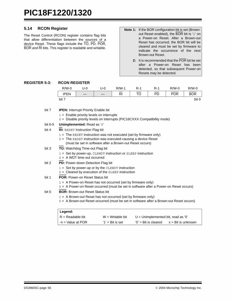
PIC18F1220/1320
5.14 RCON Register
The Reset Control (RCON) register contains flag bitsthat allow differentiation between the sources of adevice Reset. These flags include the TO, PD, POR,BOR and RI bits. This register is readable and writable.
REGISTER 5-3: RCON REGISTER
Note 1: If the BOR configuration bit is set (Brown-out Reset enabled), the BOR bit is ‘1’ ona Power-on Reset. After a Brown-outReset has occurred, the BOR bit will becleared and must be set by firmware toindicate the occurrence of the nextBrown-out Reset.
2: It is recommended that the POR bit be setafter a Power-on Reset has beendetected, so that subsequent Power-onResets may be detected.
R/W-0 U-0 U-0 R/W-1 R-1 R-1 R/W-0 R/W-0
IPEN — — RI TO PD POR BOR
bit 7 bit 0
bit 7 IPEN: Interrupt Priority Enable bit 1 = Enable priority levels on interrupts0 = Disable priority levels on interrupts (PIC16CXXX Compatibility mode)
bit 6-5 Unimplemented: Read as ‘0’
bit 4 RI: RESET Instruction Flag bit1 = The RESET instruction was not executed (set by firmware only)0 = The RESET instruction was executed causing a device Reset
(must be set in software after a Brown-out Reset occurs)
bit 3 TO: Watchdog Time-out Flag bit
1 = Set by power-up, CLRWDT instruction or SLEEP instruction 0 = A WDT time-out occurred
bit 2 PD: Power-down Detection Flag bit 1 = Set by power-up or by the CLRWDT instruction 0 = Cleared by execution of the SLEEP instruction
bit 1 POR: Power-on Reset Status bit 1 = A Power-on Reset has not occurred (set by firmware only)0 = A Power-on Reset occurred (must be set in software after a Power-on Reset occurs)
bit 0 BOR: Brown-out Reset Status bit
1 = A Brown-out Reset has not occurred (set by firmware only)0 = A Brown-out Reset occurred (must be set in software after a Brown-out Reset occurs)
Legend:
R = Readable bit W = Writable bit U = Unimplemented bit, read as ‘0’
-n = Value at POR ‘1’ = Bit is set ‘0’ = Bit is cleared x = Bit is unknown
DS39605C-page 56 2004 Microchip Technology Inc.
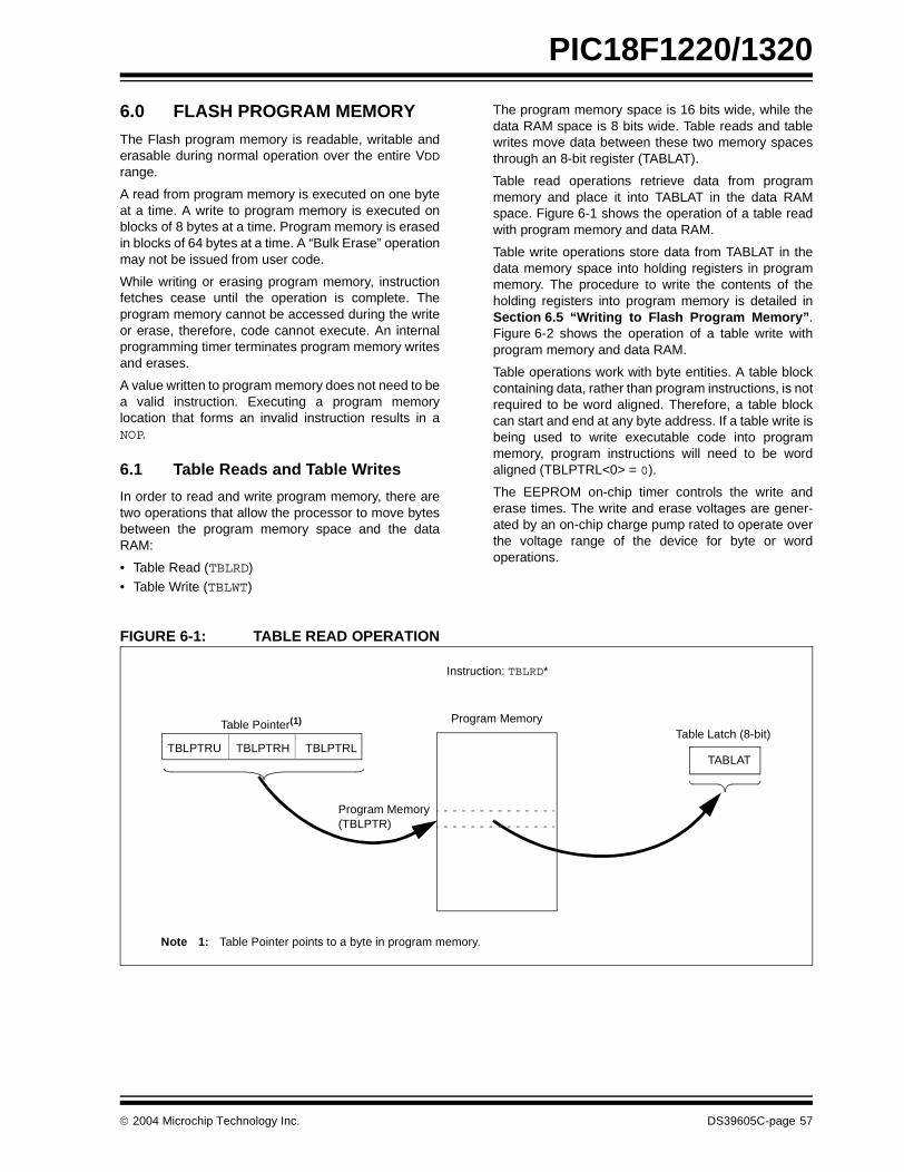
PIC18F1220/1320
6.0 FLASH PROGRAM MEMORY
The Flash program memory is readable, writable anderasable during normal operation over the entire VDD
range.
A read from program memory is executed on one byteat a time. A write to program memory is executed onblocks of 8 bytes at a time. Program memory is erasedin blocks of 64 bytes at a time. A “Bulk Erase” operationmay not be issued from user code.
While writing or erasing program memory, instructionfetches cease until the operation is complete. Theprogram memory cannot be accessed during the writeor erase, therefore, code cannot execute. An internalprogramming timer terminates program memory writesand erases.
A value written to program memory does not need to bea valid instruction. Executing a program memorylocation that forms an invalid instruction results in aNOP.
6.1 Table Reads and Table Writes
In order to read and write program memory, there aretwo operations that allow the processor to move bytesbetween the program memory space and the dataRAM:
• Table Read (TBLRD)• Table Write (TBLWT)
The program memory space is 16 bits wide, while thedata RAM space is 8 bits wide. Table reads and tablewrites move data between these two memory spacesthrough an 8-bit register (TABLAT).
Table read operations retrieve data from programmemory and place it into TABLAT in the data RAMspace. Figure 6-1 shows the operation of a table readwith program memory and data RAM.
Table write operations store data from TABLAT in thedata memory space into holding registers in programmemory. The procedure to write the contents of theholding registers into program memory is detailed inSection 6.5 “Writing to Flash Program Memory”.Figure 6-2 shows the operation of a table write withprogram memory and data RAM.
Table operations work with byte entities. A table blockcontaining data, rather than program instructions, is notrequired to be word aligned. Therefore, a table blockcan start and end at any byte address. If a table write isbeing used to write executable code into programmemory, program instructions will need to be wordaligned (TBLPTRL<0> = 0).
The EEPROM on-chip timer controls the write anderase times. The write and erase voltages are gener-ated by an on-chip charge pump rated to operate overthe voltage range of the device for byte or wordoperations.
FIGURE 6-1: TABLE READ OPERATION
Table Pointer(1)
Table Latch (8-bit)Program Memory
TBLPTRH TBLPTRLTABLAT
TBLPTRU
Instruction: TBLRD*
Note 1: Table Pointer points to a byte in program memory.
Program Memory(TBLPTR)
2004 Microchip Technology Inc. DS39605C-page 57
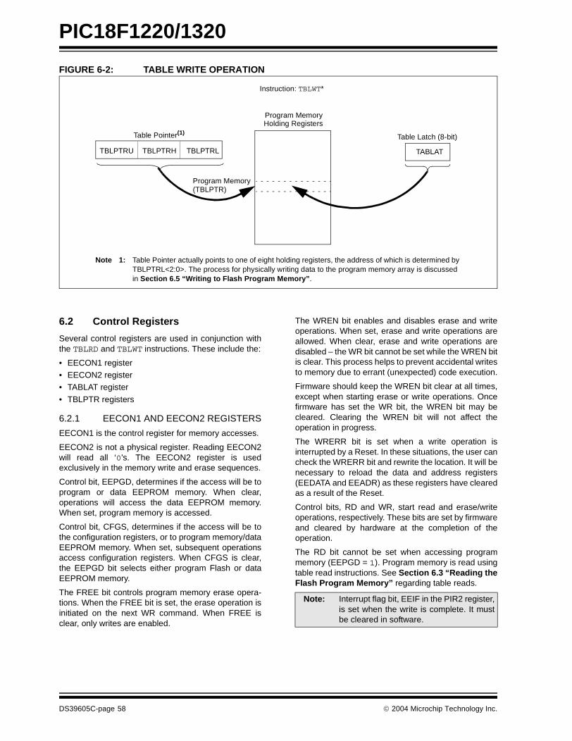
PIC18F1220/1320
FIGURE 6-2: TABLE WRITE OPERATION
6.2 Control Registers
Several control registers are used in conjunction withthe TBLRD and TBLWT instructions. These include the:
• EECON1 register• EECON2 register• TABLAT register
• TBLPTR registers
6.2.1 EECON1 AND EECON2 REGISTERS
EECON1 is the control register for memory accesses.
EECON2 is not a physical register. Reading EECON2will read all ‘0’s. The EECON2 register is usedexclusively in the memory write and erase sequences.
Control bit, EEPGD, determines if the access will be toprogram or data EEPROM memory. When clear,operations will access the data EEPROM memory.When set, program memory is accessed.
Control bit, CFGS, determines if the access will be tothe configuration registers, or to program memory/dataEEPROM memory. When set, subsequent operationsaccess configuration registers. When CFGS is clear,the EEPGD bit selects either program Flash or dataEEPROM memory.
The FREE bit controls program memory erase opera-tions. When the FREE bit is set, the erase operation isinitiated on the next WR command. When FREE isclear, only writes are enabled.
The WREN bit enables and disables erase and writeoperations. When set, erase and write operations areallowed. When clear, erase and write operations aredisabled – the WR bit cannot be set while the WREN bitis clear. This process helps to prevent accidental writesto memory due to errant (unexpected) code execution.
Firmware should keep the WREN bit clear at all times,except when starting erase or write operations. Oncefirmware has set the WR bit, the WREN bit may becleared. Clearing the WREN bit will not affect theoperation in progress.
The WRERR bit is set when a write operation isinterrupted by a Reset. In these situations, the user cancheck the WRERR bit and rewrite the location. It will benecessary to reload the data and address registers(EEDATA and EEADR) as these registers have clearedas a result of the Reset.
Control bits, RD and WR, start read and erase/writeoperations, respectively. These bits are set by firmwareand cleared by hardware at the completion of theoperation.
The RD bit cannot be set when accessing programmemory (EEPGD = 1). Program memory is read usingtable read instructions. See Section 6.3 “Reading theFlash Program Memory” regarding table reads.
Table Pointer(1)Table Latch (8-bit)
TBLPTRH TBLPTRL TABLAT
Program Memory(TBLPTR)
TBLPTRU
Instruction: TBLWT*
Note 1: Table Pointer actually points to one of eight holding registers, the address of which is determined by TBLPTRL<2:0>. The process for physically writing data to the program memory array is discussed in Section 6.5 “Writing to Flash Program Memory”.
Holding Registers Program Memory
Note: Interrupt flag bit, EEIF in the PIR2 register,is set when the write is complete. It mustbe cleared in software.
DS39605C-page 58 2004 Microchip Technology Inc.
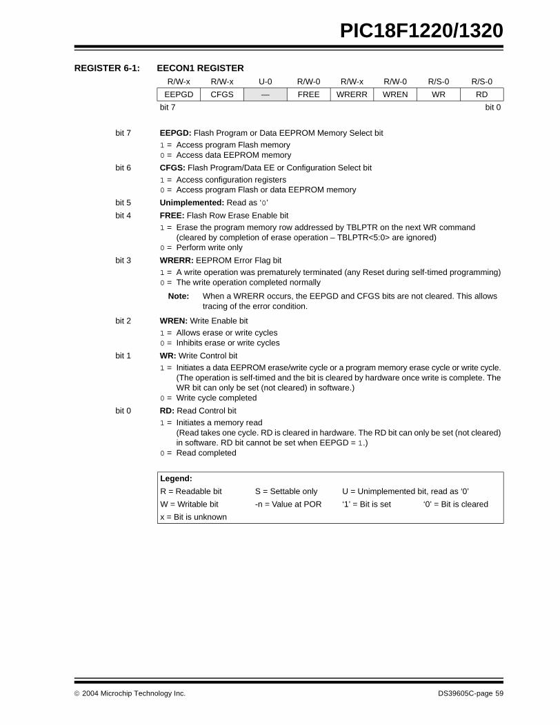
PIC18F1220/1320
REGISTER 6-1: EECON1 REGISTER R/W-x R/W-x U-0 R/W-0 R/W-x R/W-0 R/S-0 R/S-0
EEPGD CFGS — FREE WRERR WREN WR RD
bit 7 bit 0
bit 7 EEPGD: Flash Program or Data EEPROM Memory Select bit1 = Access program Flash memory0 = Access data EEPROM memory
bit 6 CFGS: Flash Program/Data EE or Configuration Select bit
1 = Access configuration registers0 = Access program Flash or data EEPROM memory
bit 5 Unimplemented: Read as ‘0’
bit 4 FREE: Flash Row Erase Enable bit1 = Erase the program memory row addressed by TBLPTR on the next WR command
(cleared by completion of erase operation – TBLPTR<5:0> are ignored)0 = Perform write only
bit 3 WRERR: EEPROM Error Flag bit1 = A write operation was prematurely terminated (any Reset during self-timed programming)0 = The write operation completed normally
Note: When a WRERR occurs, the EEPGD and CFGS bits are not cleared. This allows tracing of the error condition.
bit 2 WREN: Write Enable bit1 = Allows erase or write cycles0 = Inhibits erase or write cycles
bit 1 WR: Write Control bit1 = Initiates a data EEPROM erase/write cycle or a program memory erase cycle or write cycle.
(The operation is self-timed and the bit is cleared by hardware once write is complete. TheWR bit can only be set (not cleared) in software.)
0 = Write cycle completed
bit 0 RD: Read Control bit1 = Initiates a memory read
(Read takes one cycle. RD is cleared in hardware. The RD bit can only be set (not cleared)in software. RD bit cannot be set when EEPGD = 1.)
0 = Read completed
Legend:
R = Readable bit S = Settable only U = Unimplemented bit, read as ‘0’
W = Writable bit -n = Value at POR ‘1’ = Bit is set ‘0’ = Bit is cleared
x = Bit is unknown
2004 Microchip Technology Inc. DS39605C-page 59
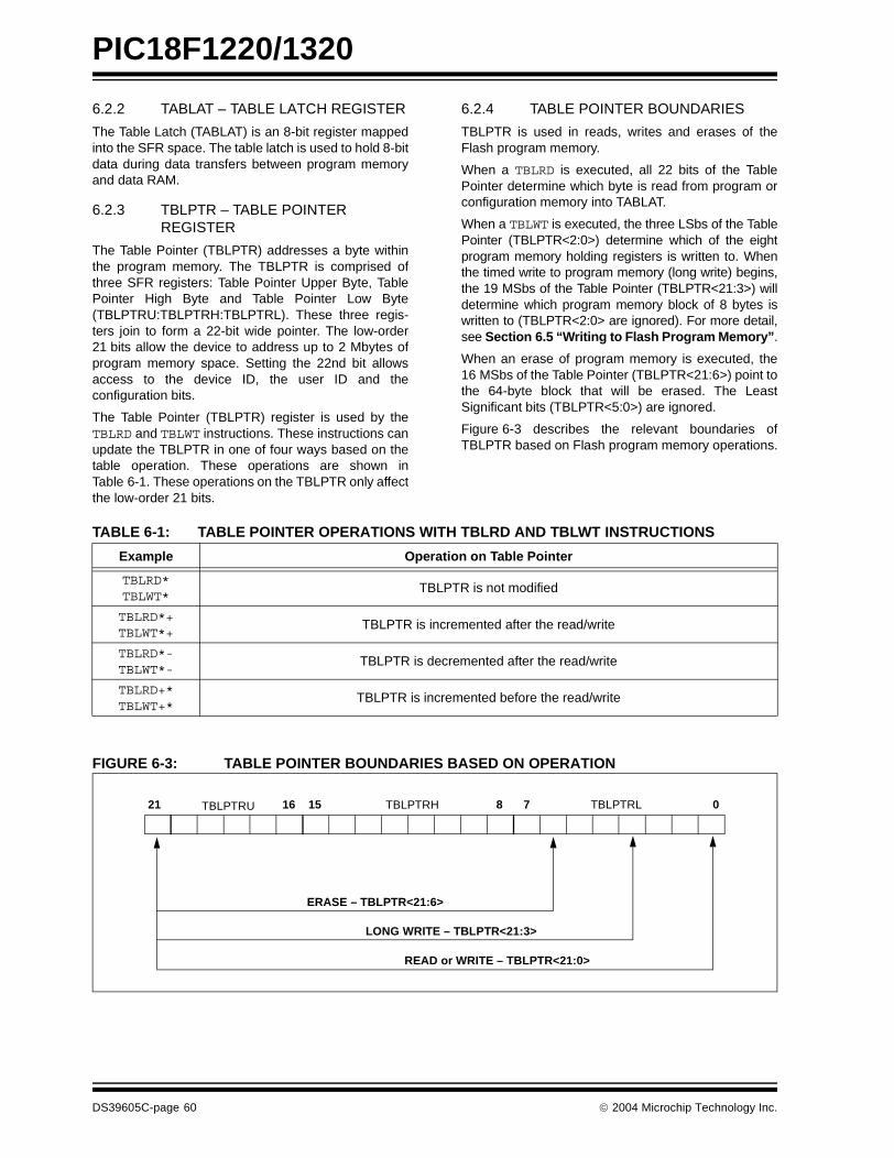
PIC18F1220/1320
6.2.2 TABLAT – TABLE LATCH REGISTER
The Table Latch (TABLAT) is an 8-bit register mappedinto the SFR space. The table latch is used to hold 8-bitdata during data transfers between program memoryand data RAM.
6.2.3 TBLPTR – TABLE POINTER REGISTER
The Table Pointer (TBLPTR) addresses a byte withinthe program memory. The TBLPTR is comprised ofthree SFR registers: Table Pointer Upper Byte, TablePointer High Byte and Table Pointer Low Byte(TBLPTRU:TBLPTRH:TBLPTRL). These three regis-ters join to form a 22-bit wide pointer. The low-order21 bits allow the device to address up to 2 Mbytes ofprogram memory space. Setting the 22nd bit allowsaccess to the device ID, the user ID and theconfiguration bits.
The Table Pointer (TBLPTR) register is used by theTBLRD and TBLWT instructions. These instructions canupdate the TBLPTR in one of four ways based on thetable operation. These operations are shown inTable 6-1. These operations on the TBLPTR only affectthe low-order 21 bits.
6.2.4 TABLE POINTER BOUNDARIES
TBLPTR is used in reads, writes and erases of theFlash program memory.
When a TBLRD is executed, all 22 bits of the TablePointer determine which byte is read from program orconfiguration memory into TABLAT.
When a TBLWT is executed, the three LSbs of the TablePointer (TBLPTR<2:0>) determine which of the eightprogram memory holding registers is written to. Whenthe timed write to program memory (long write) begins,the 19 MSbs of the Table Pointer (TBLPTR<21:3>) willdetermine which program memory block of 8 bytes iswritten to (TBLPTR<2:0> are ignored). For more detail,see Section 6.5 “Writing to Flash Program Memory”.
When an erase of program memory is executed, the16 MSbs of the Table Pointer (TBLPTR<21:6>) point tothe 64-byte block that will be erased. The LeastSignificant bits (TBLPTR<5:0>) are ignored.
Figure 6-3 describes the relevant boundaries ofTBLPTR based on Flash program memory operations.
TABLE 6-1: TABLE POINTER OPERATIONS WITH TBLRD AND TBLWT INSTRUCTIONS
FIGURE 6-3: TABLE POINTER BOUNDARIES BASED ON OPERATION
Example Operation on Table Pointer
TBLRD*TBLWT*
TBLPTR is not modified
TBLRD*+TBLWT*+
TBLPTR is incremented after the read/write
TBLRD*-TBLWT*-
TBLPTR is decremented after the read/write
TBLRD+*TBLWT+*
TBLPTR is incremented before the read/write
21 16 15 8 7 0
ERASE – TBLPTR<21:6>
LONG WRITE – TBLPTR<21:3>
READ or WRITE – TBLPTR<21:0>
TBLPTRLTBLPTRHTBLPTRU
DS39605C-page 60 2004 Microchip Technology Inc.

PIC18F1220/1320
6.3 Reading the Flash Program Memory
The TBLRD instruction is used to retrieve data fromprogram memory and place it into data RAM. Tablereads from program memory are performed one byte ata time.
TBLPTR points to a byte address in program space.Executing a TBLRD instruction places the byte pointedto into TABLAT. In addition, TBLPTR can be modifiedautomatically for the next table read operation.
The internal program memory is typically organized bywords. The Least Significant bit of the address selectsbetween the high and low bytes of the word. Figure 6-4shows the interface between the internal programmemory and the TABLAT.
FIGURE 6-4: READS FROM FLASH PROGRAM MEMORY
EXAMPLE 6-1: READING A FLASH PROGRAM MEMORY WORD
Odd (High) Byte
Program Memory
Even (Low) Byte
TABLAT
TBLPTR
Instruction Register (IR) Read Register
LSB = 1TBLPTRLSB = 0
MOVLW CODE_ADDR_UPPER ; Load TBLPTR with the baseMOVWF TBLPTRU ; address of the wordMOVLW CODE_ADDR_HIGHMOVWF TBLPTRHMOVLW CODE_ADDR_LOWMOVWF TBLPTRL
READ_WORDTBLRD*+ ; read into TABLAT and increment TBLPTRMOVFW TABLAT ; get dataMOVWF WORD_EVENTBLRD*+ ; read into TABLAT and increment TBLPTRMOVFW TABLAT ; get dataMOVWF WORD_ODD
2004 Microchip Technology Inc. DS39605C-page 61
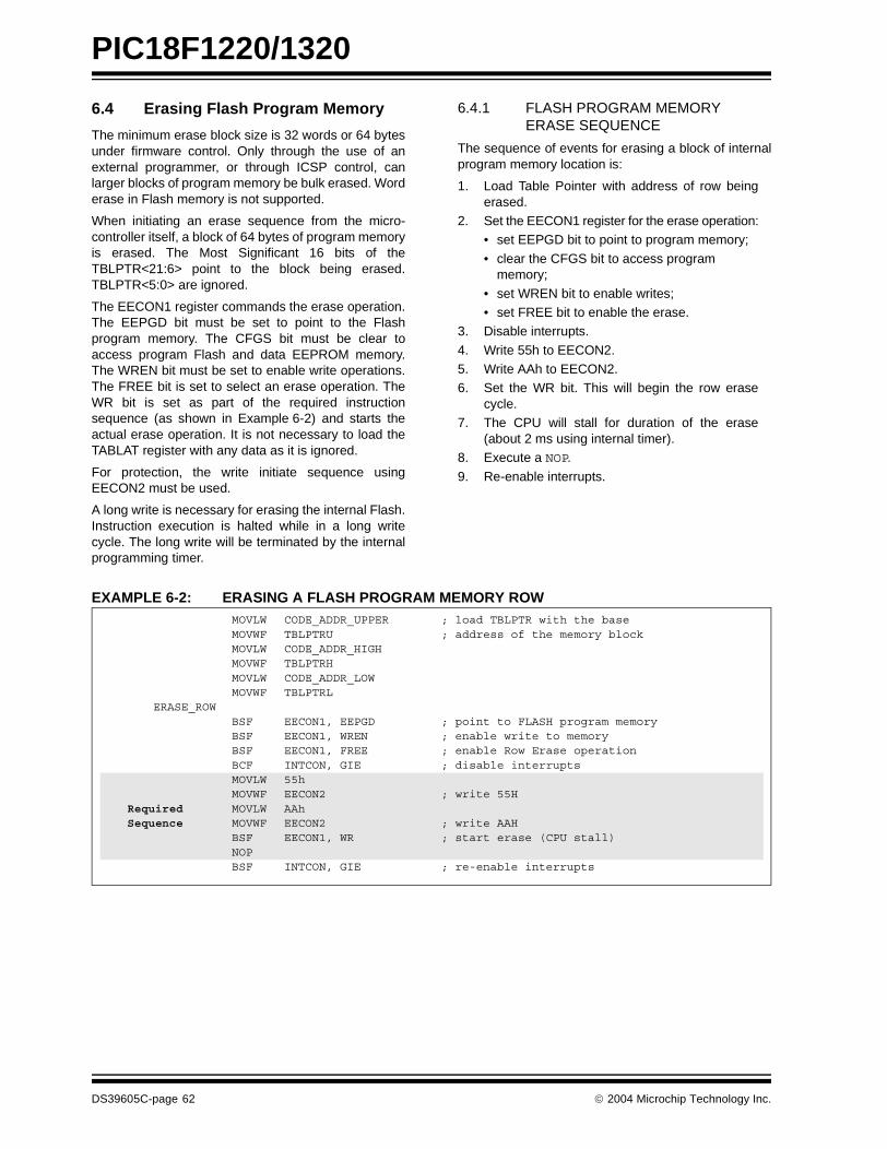
PIC18F1220/1320
6.4 Erasing Flash Program Memory
The minimum erase block size is 32 words or 64 bytesunder firmware control. Only through the use of anexternal programmer, or through ICSP control, canlarger blocks of program memory be bulk erased. Worderase in Flash memory is not supported.
When initiating an erase sequence from the micro-controller itself, a block of 64 bytes of program memoryis erased. The Most Significant 16 bits of theTBLPTR<21:6> point to the block being erased.TBLPTR<5:0> are ignored.
The EECON1 register commands the erase operation.The EEPGD bit must be set to point to the Flashprogram memory. The CFGS bit must be clear toaccess program Flash and data EEPROM memory.The WREN bit must be set to enable write operations.The FREE bit is set to select an erase operation. TheWR bit is set as part of the required instructionsequence (as shown in Example 6-2) and starts theactual erase operation. It is not necessary to load theTABLAT register with any data as it is ignored.
For protection, the write initiate sequence usingEECON2 must be used.
A long write is necessary for erasing the internal Flash.Instruction execution is halted while in a long writecycle. The long write will be terminated by the internalprogramming timer.
6.4.1 FLASH PROGRAM MEMORY ERASE SEQUENCE
The sequence of events for erasing a block of internalprogram memory location is:
1. Load Table Pointer with address of row beingerased.
2. Set the EECON1 register for the erase operation:• set EEPGD bit to point to program memory;
• clear the CFGS bit to access program memory;
• set WREN bit to enable writes;• set FREE bit to enable the erase.
3. Disable interrupts.
4. Write 55h to EECON2.5. Write AAh to EECON2.6. Set the WR bit. This will begin the row erase
cycle.7. The CPU will stall for duration of the erase
(about 2 ms using internal timer).8. Execute a NOP.
9. Re-enable interrupts.
EXAMPLE 6-2: ERASING A FLASH PROGRAM MEMORY ROW MOVLW CODE_ADDR_UPPER ; load TBLPTR with the baseMOVWF TBLPTRU ; address of the memory blockMOVLW CODE_ADDR_HIGHMOVWF TBLPTRH MOVLW CODE_ADDR_LOWMOVWF TBLPTRL
ERASE_ROW BSF EECON1, EEPGD ; point to FLASH program memoryBSF EECON1, WREN ; enable write to memoryBSF EECON1, FREE ; enable Row Erase operationBCF INTCON, GIE ; disable interruptsMOVLW 55hMOVWF EECON2 ; write 55H
Required MOVLW AAhSequence MOVWF EECON2 ; write AAH
BSF EECON1, WR ; start erase (CPU stall)NOPBSF INTCON, GIE ; re-enable interrupts
DS39605C-page 62 2004 Microchip Technology Inc.
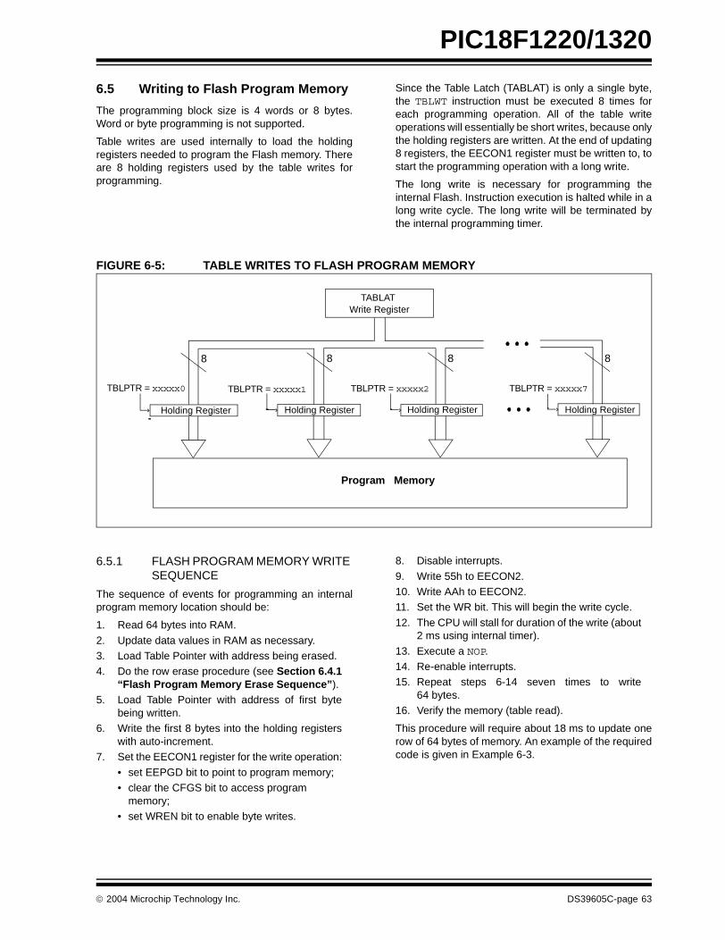
PIC18F1220/1320
6.5 Writing to Flash Program Memory
The programming block size is 4 words or 8 bytes.Word or byte programming is not supported.
Table writes are used internally to load the holdingregisters needed to program the Flash memory. Thereare 8 holding registers used by the table writes forprogramming.
Since the Table Latch (TABLAT) is only a single byte,the TBLWT instruction must be executed 8 times foreach programming operation. All of the table writeoperations will essentially be short writes, because onlythe holding registers are written. At the end of updating8 registers, the EECON1 register must be written to, tostart the programming operation with a long write.
The long write is necessary for programming theinternal Flash. Instruction execution is halted while in along write cycle. The long write will be terminated bythe internal programming timer.
FIGURE 6-5: TABLE WRITES TO FLASH PROGRAM MEMORY
6.5.1 FLASH PROGRAM MEMORY WRITE SEQUENCE
The sequence of events for programming an internalprogram memory location should be:
1. Read 64 bytes into RAM.
2. Update data values in RAM as necessary.3. Load Table Pointer with address being erased.4. Do the row erase procedure (see Section 6.4.1
“Flash Program Memory Erase Sequence”).5. Load Table Pointer with address of first byte
being written.6. Write the first 8 bytes into the holding registers
with auto-increment.7. Set the EECON1 register for the write operation:
• set EEPGD bit to point to program memory;• clear the CFGS bit to access program
memory;• set WREN bit to enable byte writes.
8. Disable interrupts.
9. Write 55h to EECON2.10. Write AAh to EECON2.11. Set the WR bit. This will begin the write cycle.
12. The CPU will stall for duration of the write (about2 ms using internal timer).
13. Execute a NOP.14. Re-enable interrupts.15. Repeat steps 6-14 seven times to write
64 bytes.16. Verify the memory (table read).
This procedure will require about 18 ms to update onerow of 64 bytes of memory. An example of the requiredcode is given in Example 6-3.
Holding Register
TABLAT
Holding Register
TBLPTR = xxxxx7
Holding Register
TBLPTR = xxxxx1
Holding Register
TBLPTR = xxxxx0
8 8 8 8
Write Register
TBLPTR = xxxxx2
Program Memory
2004 Microchip Technology Inc. DS39605C-page 63
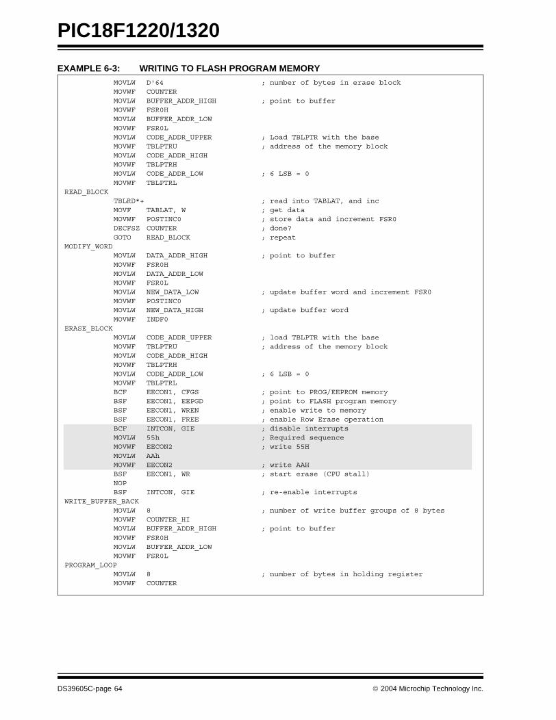
PIC18F1220/1320
EXAMPLE 6-3: WRITING TO FLASH PROGRAM MEMORYMOVLW D'64 ; number of bytes in erase blockMOVWF COUNTERMOVLW BUFFER_ADDR_HIGH ; point to bufferMOVWF FSR0HMOVLW BUFFER_ADDR_LOWMOVWF FSR0LMOVLW CODE_ADDR_UPPER ; Load TBLPTR with the baseMOVWF TBLPTRU ; address of the memory blockMOVLW CODE_ADDR_HIGHMOVWF TBLPTRHMOVLW CODE_ADDR_LOW ; 6 LSB = 0MOVWF TBLPTRL
READ_BLOCKTBLRD*+ ; read into TABLAT, and incMOVF TABLAT, W ; get dataMOVWF POSTINC0 ; store data and increment FSR0DECFSZ COUNTER ; done?GOTO READ_BLOCK ; repeat
MODIFY_WORDMOVLW DATA_ADDR_HIGH ; point to bufferMOVWF FSR0HMOVLW DATA_ADDR_LOWMOVWF FSR0LMOVLW NEW_DATA_LOW ; update buffer word and increment FSR0MOVWF POSTINC0MOVLW NEW_DATA_HIGH ; update buffer wordMOVWF INDF0
ERASE_BLOCKMOVLW CODE_ADDR_UPPER ; load TBLPTR with the baseMOVWF TBLPTRU ; address of the memory blockMOVLW CODE_ADDR_HIGHMOVWF TBLPTRH MOVLW CODE_ADDR_LOW ; 6 LSB = 0MOVWF TBLPTRLBCF EECON1, CFGS ; point to PROG/EEPROM memory BSF EECON1, EEPGD ; point to FLASH program memoryBSF EECON1, WREN ; enable write to memoryBSF EECON1, FREE ; enable Row Erase operationBCF INTCON, GIE ; disable interruptsMOVLW 55h ; Required sequenceMOVWF EECON2 ; write 55HMOVLW AAhMOVWF EECON2 ; write AAHBSF EECON1, WR ; start erase (CPU stall)NOPBSF INTCON, GIE ; re-enable interrupts
WRITE_BUFFER_BACKMOVLW 8 ; number of write buffer groups of 8 bytesMOVWF COUNTER_HIMOVLW BUFFER_ADDR_HIGH ; point to bufferMOVWF FSR0HMOVLW BUFFER_ADDR_LOWMOVWF FSR0L
PROGRAM_LOOPMOVLW 8 ; number of bytes in holding registerMOVWF COUNTER
DS39605C-page 64 2004 Microchip Technology Inc.
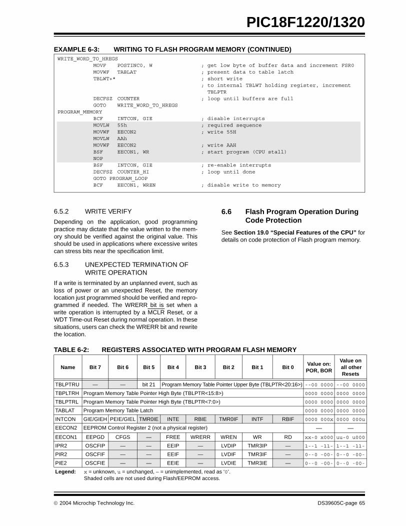
PIC18F1220/1320
EXAMPLE 6-3: WRITING TO FLASH PROGRAM MEMORY (CONTINUED)
6.5.2 WRITE VERIFY
Depending on the application, good programmingpractice may dictate that the value written to the mem-ory should be verified against the original value. Thisshould be used in applications where excessive writescan stress bits near the specification limit.
6.5.3 UNEXPECTED TERMINATION OF WRITE OPERATION
If a write is terminated by an unplanned event, such asloss of power or an unexpected Reset, the memorylocation just programmed should be verified and repro-grammed if needed. The WRERR bit is set when awrite operation is interrupted by a MCLR Reset, or aWDT Time-out Reset during normal operation. In thesesituations, users can check the WRERR bit and rewritethe location.
6.6 Flash Program Operation During Code Protection
See Section 19.0 “Special Features of the CPU” fordetails on code protection of Flash program memory.
TABLE 6-2: REGISTERS ASSOCIATED WITH PROGRAM FLASH MEMORY
WRITE_WORD_TO_HREGSMOVF POSTINC0, W ; get low byte of buffer data and increment FSR0MOVWF TABLAT ; present data to table latchTBLWT+* ; short write
; to internal TBLWT holding register, increment TBLPTR
DECFSZ COUNTER ; loop until buffers are fullGOTO WRITE_WORD_TO_HREGS
PROGRAM_MEMORYBCF INTCON, GIE ; disable interruptsMOVLW 55h ; required sequenceMOVWF EECON2 ; write 55HMOVLW AAhMOVWF EECON2 ; write AAHBSF EECON1, WR ; start program (CPU stall)NOPBSF INTCON, GIE ; re-enable interruptsDECFSZ COUNTER_HI ; loop until doneGOTO PROGRAM_LOOPBCF EECON1, WREN ; disable write to memory
Name Bit 7 Bit 6 Bit 5 Bit 4 Bit 3 Bit 2 Bit 1 Bit 0Value on:POR, BOR
Value on all other Resets
TBLPTRU — — bit 21 Program Memory Table Pointer Upper Byte (TBLPTR<20:16>) --00 0000 --00 0000
TBPLTRH Program Memory Table Pointer High Byte (TBLPTR<15:8>) 0000 0000 0000 0000
TBLPTRL Program Memory Table Pointer High Byte (TBLPTR<7:0>) 0000 0000 0000 0000
TABLAT Program Memory Table Latch 0000 0000 0000 0000
INTCON GIE/GIEH PEIE/GIEL TMR0IE INTE RBIE TMR0IF INTF RBIF 0000 000x 0000 000u
EECON2 EEPROM Control Register 2 (not a physical register) — —
EECON1 EEPGD CFGS — FREE WRERR WREN WR RD xx-0 x000 uu-0 u000
IPR2 OSCFIP — — EEIP — LVDIP TMR3IP — 1--1 -11- 1--1 -11-
PIR2 OSCFIF — — EEIF — LVDIF TMR3IF — 0--0 -00- 0--0 -00-
PIE2 OSCFIE — — EEIE — LVDIE TMR3IE — 0--0 -00- 0--0 -00-
Legend: x = unknown, u = unchanged, – = unimplemented, read as ‘0’. Shaded cells are not used during Flash/EEPROM access.
2004 Microchip Technology Inc. DS39605C-page 65

PIC18F1220/1320
NOTES:
DS39605C-page 66 2004 Microchip Technology Inc.

PIC18F1220/1320
7.0 DATA EEPROM MEMORY
The data EEPROM is readable and writable duringnormal operation over the entire VDD range. The datamemory is not directly mapped in the register filespace. Instead, it is indirectly addressed through theSpecial Function Registers (SFR).
There are four SFRs used to read and write theprogram and data EEPROM memory. These registersare:
• EECON1• EECON2• EEDATA
• EEADR
The EEPROM data memory allows byte read and write.When interfacing to the data memory block, EEDATAholds the 8-bit data for read/write and EEADR holds theaddress of the EEPROM location being accessed.These devices have 256 bytes of data EEPROM withan address range from 00h to FFh.
The EEPROM data memory is rated for high erase/write cycle endurance. A byte write automaticallyerases the location and writes the new data (erase-before-write). The write time is controlled by an on-chiptimer. The write time will vary with voltage andtemperature, as well as from chip to chip. Pleaserefer to parameter D122 (Table 22-1 in Section 22.0“Electrical Characteristics”) for exact limits.
7.1 EEADR
The address register can address 256 bytes of dataEEPROM.
7.2 EECON1 and EECON2 Registers
EECON1 is the control register for memory accesses.
EECON2 is not a physical register. Reading EECON2will read all ‘0’s. The EECON2 register is usedexclusively in the memory write and erase sequences.
Control bit, EEPGD, determines if the access will be toprogram or data EEPROM memory. When clear,operations will access the data EEPROM memory.When set, program memory is accessed.
Control bit, CFGS, determines if the access will be tothe configuration registers or to program memory/dataEEPROM memory. When set, subsequent operationsaccess configuration registers. When CFGS is clear,the EEPGD bit selects either program Flash or dataEEPROM memory.
The WREN bit enables and disables erase and writeoperations. When set, erase and write operations areallowed. When clear, erase and write operations aredisabled – the WR bit cannot be set while the WREN bitis clear. This mechanism helps to prevent accidentalwrites to memory due to errant (unexpected) codeexecution.
Firmware should keep the WREN bit clear at all times,except when starting erase or write operations. Oncefirmware has set the WR bit, the WREN bit may becleared. Clearing the WREN bit will not affect theoperation in progress.
The WRERR bit is set when a write operation isinterrupted by a Reset. In these situations, the user cancheck the WRERR bit and rewrite the location. It isnecessary to reload the data and address registers(EEDATA and EEADR), as these registers havecleared as a result of the Reset.
Control bits, RD and WR, start read and erase/writeoperations, respectively. These bits are set by firmwareand cleared by hardware at the completion of theoperation.
The RD bit cannot be set when accessing programmemory (EEPGD = 1). Program memory is read usingtable read instructions. See Section 6.1 “Table Readsand Table Writes” regarding table reads.
Note: Interrupt flag bit, EEIF in the PIR2 register,is set when write is complete. It must becleared in software.
2004 Microchip Technology Inc. DS39605C-page 67
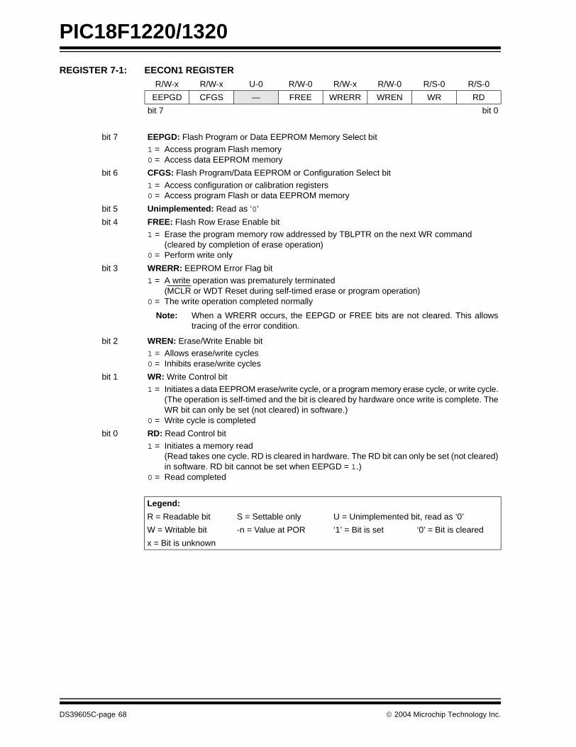
PIC18F1220/1320
REGISTER 7-1: EECON1 REGISTER R/W-x R/W-x U-0 R/W-0 R/W-x R/W-0 R/S-0 R/S-0
EEPGD CFGS — FREE WRERR WREN WR RD
bit 7 bit 0
bit 7 EEPGD: Flash Program or Data EEPROM Memory Select bit1 = Access program Flash memory0 = Access data EEPROM memory
bit 6 CFGS: Flash Program/Data EEPROM or Configuration Select bit
1 = Access configuration or calibration registers0 = Access program Flash or data EEPROM memory
bit 5 Unimplemented: Read as ‘0’
bit 4 FREE: Flash Row Erase Enable bit1 = Erase the program memory row addressed by TBLPTR on the next WR command
(cleared by completion of erase operation)0 = Perform write only
bit 3 WRERR: EEPROM Error Flag bit1 = A write operation was prematurely terminated
(MCLR or WDT Reset during self-timed erase or program operation)0 = The write operation completed normally
Note: When a WRERR occurs, the EEPGD or FREE bits are not cleared. This allowstracing of the error condition.
bit 2 WREN: Erase/Write Enable bit1 = Allows erase/write cycles0 = Inhibits erase/write cycles
bit 1 WR: Write Control bit
1 = Initiates a data EEPROM erase/write cycle, or a program memory erase cycle, or write cycle.(The operation is self-timed and the bit is cleared by hardware once write is complete. TheWR bit can only be set (not cleared) in software.)
0 = Write cycle is completed
bit 0 RD: Read Control bit
1 = Initiates a memory read (Read takes one cycle. RD is cleared in hardware. The RD bit can only be set (not cleared)in software. RD bit cannot be set when EEPGD = 1.)
0 = Read completed
Legend:
R = Readable bit S = Settable only U = Unimplemented bit, read as ‘0’
W = Writable bit -n = Value at POR ‘1’ = Bit is set ‘0’ = Bit is cleared
x = Bit is unknown
DS39605C-page 68 2004 Microchip Technology Inc.
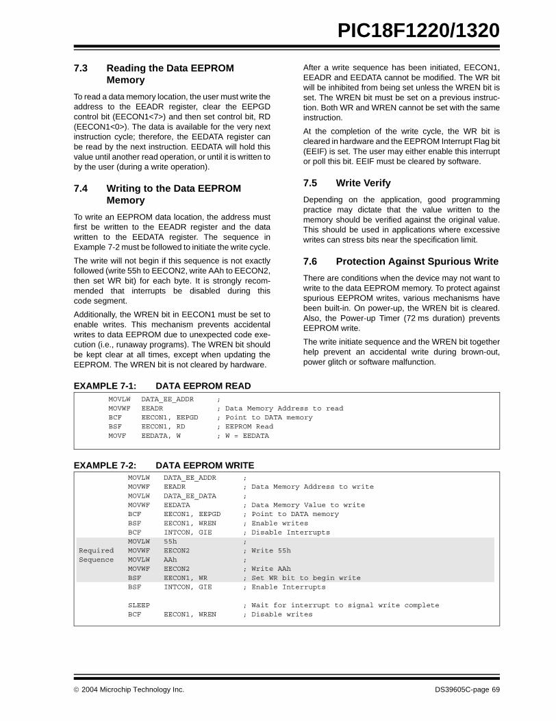
PIC18F1220/1320
7.3 Reading the Data EEPROM Memory
To read a data memory location, the user must write theaddress to the EEADR register, clear the EEPGDcontrol bit (EECON1<7>) and then set control bit, RD(EECON1<0>). The data is available for the very nextinstruction cycle; therefore, the EEDATA register canbe read by the next instruction. EEDATA will hold thisvalue until another read operation, or until it is written toby the user (during a write operation).
7.4 Writing to the Data EEPROM Memory
To write an EEPROM data location, the address mustfirst be written to the EEADR register and the datawritten to the EEDATA register. The sequence inExample 7-2 must be followed to initiate the write cycle.
The write will not begin if this sequence is not exactlyfollowed (write 55h to EECON2, write AAh to EECON2,then set WR bit) for each byte. It is strongly recom-mended that interrupts be disabled during thiscode segment.
Additionally, the WREN bit in EECON1 must be set toenable writes. This mechanism prevents accidentalwrites to data EEPROM due to unexpected code exe-cution (i.e., runaway programs). The WREN bit shouldbe kept clear at all times, except when updating theEEPROM. The WREN bit is not cleared by hardware.
After a write sequence has been initiated, EECON1,EEADR and EEDATA cannot be modified. The WR bitwill be inhibited from being set unless the WREN bit isset. The WREN bit must be set on a previous instruc-tion. Both WR and WREN cannot be set with the sameinstruction.
At the completion of the write cycle, the WR bit iscleared in hardware and the EEPROM Interrupt Flag bit(EEIF) is set. The user may either enable this interruptor poll this bit. EEIF must be cleared by software.
7.5 Write Verify
Depending on the application, good programmingpractice may dictate that the value written to thememory should be verified against the original value.This should be used in applications where excessivewrites can stress bits near the specification limit.
7.6 Protection Against Spurious Write
There are conditions when the device may not want towrite to the data EEPROM memory. To protect againstspurious EEPROM writes, various mechanisms havebeen built-in. On power-up, the WREN bit is cleared.Also, the Power-up Timer (72 ms duration) preventsEEPROM write.
The write initiate sequence and the WREN bit togetherhelp prevent an accidental write during brown-out,power glitch or software malfunction.
EXAMPLE 7-1: DATA EEPROM READ
EXAMPLE 7-2: DATA EEPROM WRITE
MOVLW DATA_EE_ADDR ;MOVWF EEADR ; Data Memory Address to readBCF EECON1, EEPGD ; Point to DATA memoryBSF EECON1, RD ; EEPROM ReadMOVF EEDATA, W ; W = EEDATA
MOVLW DATA_EE_ADDR ;MOVWF EEADR ; Data Memory Address to writeMOVLW DATA_EE_DATA ;MOVWF EEDATA ; Data Memory Value to writeBCF EECON1, EEPGD ; Point to DATA memoryBSF EECON1, WREN ; Enable writesBCF INTCON, GIE ; Disable InterruptsMOVLW 55h ;
Required MOVWF EECON2 ; Write 55hSequence MOVLW AAh ;
MOVWF EECON2 ; Write AAhBSF EECON1, WR ; Set WR bit to begin writeBSF INTCON, GIE ; Enable Interrupts
SLEEP ; Wait for interrupt to signal write completeBCF EECON1, WREN ; Disable writes
2004 Microchip Technology Inc. DS39605C-page 69

PIC18F1220/1320
7.7 Operation During Code-Protect
Data EEPROM memory has its own code-protect bits inconfiguration words. External read and writeoperations are disabled if either of these mechanismsare enabled.
The microcontroller itself can both read and write to theinternal data EEPROM, regardless of the state of thecode-protect configuration bit. Refer to Section 19.0“Special Features of the CPU” for additionalinformation.
7.8 Using the Data EEPROM
The data EEPROM is a high endurance, byte address-able array that has been optimized for the storage of fre-quently changing information (e.g., program variables orother data that are updated often). Frequently changingvalues will typically be updated more often than specifi-cation D124. If this is not the case, an array refresh mustbe performed. For this reason, variables that changeinfrequently (such as constants, IDs, calibration, etc.)should be stored in Flash program memory.
A simple data EEPROM refresh routine is shown inExample 7-3.
EXAMPLE 7-3: DATA EEPROM REFRESH ROUTINE
TABLE 7-1: REGISTERS ASSOCIATED WITH DATA EEPROM MEMORY
Note: If data EEPROM is only used to storeconstants and/or data that changes rarely,an array refresh is likely not required. Seespecification D124.
CLRF EEADR ; Start at address 0BCF EECON1, CFGS ; Set for memoryBCF EECON1, EEPGD ; Set for Data EEPROMBCF INTCON, GIE ; Disable interruptsBSF EECON1, WREN ; Enable writes
Loop ; Loop to refresh arrayBSF EECON1, RD ; Read current addressMOVLW 55h ;MOVWF EECON2 ; Write 55hMOVLW AAh ;MOVWF EECON2 ; Write AAhBSF EECON1, WR ; Set WR bit to begin writeBTFSC EECON1, WR ; Wait for write to completeBRA $-2INCFSZ EEADR, F ; Increment addressBRA Loop ; Not zero, do it again
BCF EECON1, WREN ; Disable writesBSF INTCON, GIE ; Enable interrupts
Name Bit 7 Bit 6 Bit 5 Bit 4 Bit 3 Bit 2 Bit 1 Bit 0Value on:POR, BOR
Value on all other Resets
INTCON GIE/GIEH PEIE/GIEL TMR0IE INTE RBIE TMR0IF INTF RBIF 0000 000x 0000 000u
EEADR EEPROM Address Register 0000 0000 0000 0000
EEDATA EEPROM Data Register 0000 0000 0000 0000
EECON2 EEPROM Control Register 2 (not a physical register) — —
EECON1 EEPGD CFGS — FREE WRERR WREN WR RD xx-0 x000 uu-0 u000
IPR2 OSCFIP — — EEIP — LVDIP TMR3IP — 1--1 -11- 1--1 -11-
PIR2 OSCFIF — — EEIF — LVDIF TMR3IF — 0--0 -00- 0--0 -00-
PIE2 OSCFIE — — EEIE — LVDIE TMR3IE — 0--0 -00- 0--0 -00-
Legend: x = unknown, u = unchanged, – = unimplemented, read as ‘0’. Shaded cells are not used during Flash/EEPROM access.
DS39605C-page 70 2004 Microchip Technology Inc.

PIC18F1220/1320
8.0 8 x 8 HARDWARE MULTIPLIER
8.1 Introduction
An 8 x 8 hardware multiplier is included in the ALU ofthe PIC18F1220/1320 devices. By making the multiplya hardware operation, it completes in a single instruc-tion cycle. This is an unsigned multiply that gives a16-bit result. The result is stored into the 16-bit productregister pair (PRODH:PRODL). The multiplier does notaffect any flags in the Status register.
Making the 8 x 8 multiplier execute in a single cyclegives the following advantages:
• Higher computational throughput• Reduces code size requirements for multiply
algorithms
The performance increase allows the device to be usedin applications previously reserved for Digital SignalProcessors.
Table 8-1 shows a performance comparison betweenEnhanced devices using the single-cycle hardwaremultiply and performing the same function without thehardware multiply.
TABLE 8-1: PERFORMANCE COMPARISON
8.2 Operation
Example 8-1 shows the sequence to do an 8 x 8unsigned multiply. Only one instruction is requiredwhen one argument of the multiply is already loaded inthe WREG register.
Example 8-2 shows the sequence to do an 8 x 8 signedmultiply. To account for the sign bits of the arguments,each argument’s Most Significant bit (MSb) is testedand the appropriate subtractions are done.
EXAMPLE 8-1: 8 x 8 UNSIGNED MULTIPLY ROUTINE
EXAMPLE 8-2: 8 x 8 SIGNED MULTIPLY ROUTINE
Routine Multiply MethodProgramMemory(Words)
Cycles(Max)
Time
@ 40 MHz @ 10 MHz @ 4 MHz
8 x 8 unsignedWithout hardware multiply 13 69 6.9 µs 27.6 µs 69 µs
Hardware multiply 1 1 100 ns 400 ns 1 µs
8 x 8 signedWithout hardware multiply 33 91 9.1 µs 36.4 µs 91 µs
Hardware multiply 6 6 600 ns 2.4 µs 6 µs
16 x 16 unsignedWithout hardware multiply 21 242 24.2 µs 96.8 µs 242 µs
Hardware multiply 28 28 2.8 µs 11.2 µs 28 µs
16 x 16 signedWithout hardware multiply 52 254 25.4 µs 102.6 µs 254 µs
Hardware multiply 35 40 4 µs 16 µs 40 µs
MOVF ARG1, W ; MULWF ARG2 ; ARG1 * ARG2 ->
; PRODH:PRODL
MOVF ARG1, W MULWF ARG2 ; ARG1 * ARG2 ->
; PRODH:PRODL BTFSC ARG2, SB ; Test Sign Bit SUBWF PRODH, F ; PRODH = PRODH
; - ARG1 MOVF ARG2, W BTFSC ARG1, SB ; Test Sign Bit SUBWF PRODH, F ; PRODH = PRODH
; - ARG2
2004 Microchip Technology Inc. DS39605C-page 71

PIC18F1220/1320
Example 8-3 shows the sequence to do a 16 x 16unsigned multiply. Equation 8-1 shows the algorithmthat is used. The 32-bit result is stored in four registers,RES3:RES0.
EQUATION 8-1: 16 x 16 UNSIGNED MULTIPLICATION ALGORITHM
EXAMPLE 8-3: 16 x 16 UNSIGNED MULTIPLY ROUTINE
Example 8-4 shows the sequence to do a 16 x 16signed multiply. Equation 8-2 shows the algorithmused. The 32-bit result is stored in four registers,RES3:RES0. To account for the sign bits of the argu-ments, each argument pairs’ Most Significant bit (MSb)is tested and the appropriate subtractions are done.
EQUATION 8-2: 16 x 16 SIGNED MULTIPLICATION ALGORITHM
EXAMPLE 8-4: 16 x 16 SIGNED MULTIPLY ROUTINE
MOVF ARG1L, W MULWF ARG2L ; ARG1L * ARG2L ->
; PRODH:PRODL MOVFF PRODH, RES1 ; MOVFF PRODL, RES0 ;
; MOVF ARG1H, W MULWF ARG2H ; ARG1H * ARG2H ->
; PRODH:PRODL MOVFF PRODH, RES3 ; MOVFF PRODL, RES2 ;
; MOVF ARG1L, W MULWF ARG2H ; ARG1L * ARG2H ->
; PRODH:PRODL MOVF PRODL, W ; ADDWF RES1, F ; Add cross MOVF PRODH, W ; products ADDWFC RES2, F ; CLRF WREG ; ADDWFC RES3,F ;
; MOVF ARG1H, W ; MULWF ARG2L ; ARG1H * ARG2L ->
; PRODH:PRODL MOVF PRODL, W ; ADDWF RES1, F ; Add cross MOVF PRODH, W ; products ADDWFC RES2, F ; CLRF WREG ; ADDWFC RES3, F ;
RES3:RES0= ARG1H:ARG1L • ARG2H:ARG2L= (ARG1H • ARG2H • 216) +
(ARG1H • ARG2L • 28) +(ARG1L • ARG2H • 28) +(ARG1L • ARG2L)
MOVF ARG1L, W MULWF ARG2L ; ARG1L * ARG2L ->
; PRODH:PRODL MOVFF PRODH, RES1 ; MOVFF PRODL, RES0 ;
; MOVF ARG1H, W MULWF ARG2H ; ARG1H * ARG2H ->
; PRODH:PRODL MOVFF PRODH, RES3 ; MOVFF PRODL, RES2 ;
; MOVF ARG1L, W MULWF ARG2H ; ARG1L * ARG2H ->
; PRODH:PRODL MOVF PRODL, W ; ADDWF RES1, F ; Add cross MOVF PRODH, W ; products ADDWFC RES2, F ; CLRF WREG ; ADDWFC RES3, F ;
; MOVF ARG1H, W ; MULWF ARG2L ; ARG1H * ARG2L ->
; PRODH:PRODL MOVF PRODL, W ; ADDWF RES1, F ; Add cross MOVF PRODH, W ; products ADDWFC RES2, F ; CLRF WREG ; ADDWFC RES3, F ;
; BTFSS ARG2H, 7 ; ARG2H:ARG2L neg? BRA SIGN_ARG1 ; no, check ARG1 MOVF ARG1L, W ; SUBWF RES2 ; MOVF ARG1H, W ; SUBWFB RES3
; SIGN_ARG1
BTFSS ARG1H, 7 ; ARG1H:ARG1L neg? BRA CONT_CODE ; no, done MOVF ARG2L, W ; SUBWF RES2 ; MOVF ARG2H, W ; SUBWFB RES3
; CONT_CODE :
RES3:RES0= ARG1H:ARG1L • ARG2H:ARG2L= (ARG1H • ARG2H • 216) +
(ARG1H • ARG2L • 28) +(ARG1L • ARG2H • 28) +(ARG1L • ARG2L) +(-1 • ARG2H<7> • ARG1H:ARG1L • 216) +(-1 • ARG1H<7> • ARG2H:ARG2L • 216)
DS39605C-page 72 2004 Microchip Technology Inc.
PIC18F1220/1320
9.0 INTERRUPTS
The PIC18F1220/1320 devices have multiple interruptsources and an interrupt priority feature that allowseach interrupt source to be assigned a high prioritylevel or a low priority level. The high priority interruptvector is at 000008h and the low priority interrupt vectoris at 000018h. High priority interrupt events willinterrupt any low priority interrupts that may be inprogress.
There are ten registers which are used to controlinterrupt operation. These registers are:
• RCON• INTCON
• INTCON2• INTCON3• PIR1, PIR2
• PIE1, PIE2• IPR1, IPR2
It is recommended that the Microchip header filessupplied with MPLAB® IDE be used for the symbolic bitnames in these registers. This allows the assembler/compiler to automatically take care of the placement ofthese bits within the specified register.
In general, each interrupt source has three bits tocontrol its operation. The functions of these bits are:
• Flag bit to indicate that an interrupt event occurred
• Enable bit that allows program execution to branch to the interrupt vector address when the flag bit is set
• Priority bit to select high priority or low priority (INT0 has no priority bit and is always high priority)
The interrupt priority feature is enabled by setting theIPEN bit (RCON<7>). When interrupt priority isenabled, there are two bits which enable interruptsglobally. Setting the GIEH bit (INTCON<7>) enables allinterrupts that have the priority bit set (high priority).Setting the GIEL bit (INTCON<6>) enables allinterrupts that have the priority bit cleared (low priority).When the interrupt flag, enable bit and appropriateglobal interrupt enable bit are set, the interrupt willvector immediately to address 000008h or 000018h,depending on the priority bit setting. Individualinterrupts can be disabled through their correspondingenable bits.
When the IPEN bit is cleared (default state), theinterrupt priority feature is disabled and interrupts arecompatible with PICmicro mid-range devices. InCompatibility mode, the interrupt priority bits for eachsource have no effect. INTCON<6> is the PEIE bit,which enables/disables all peripheral interrupt sources.INTCON<7> is the GIE bit, which enables/disables allinterrupt sources. All interrupts branch to address000008h in Compatibility mode.
When an interrupt is responded to, the global interruptenable bit is cleared to disable further interrupts. If theIPEN bit is cleared, this is the GIE bit. If interrupt prioritylevels are used, this will be either the GIEH or GIEL bit.High priority interrupt sources can interrupt a lowpriority interrupt. Low priority interrupts are notprocessed while high priority interrupts are in progress.
The return address is pushed onto the stack and thePC is loaded with the interrupt vector address(000008h or 000018h). Once in the Interrupt ServiceRoutine, the source(s) of the interrupt can be deter-mined by polling the interrupt flag bits. The interruptflag bits must be cleared in software before re-enablinginterrupts to avoid recursive interrupts.
The “return from interrupt” instruction, RETFIE, exitsthe interrupt routine and sets the GIE bit (GIEH orGIEL, if priority levels are used), which re-enablesinterrupts.
For external interrupt events, such as the INT pins orthe PORTB input change interrupt, the interrupt latencywill be three to four instruction cycles. The exactlatency is the same for one or two-cycle instructions.Individual interrupt flag bits are set, regardless of thestatus of their corresponding enable bit or the GIE bit.
Note: Do not use the MOVFF instruction to modifyany of the interrupt control registers whileany interrupt is enabled. Doing so maycause erratic microcontroller behavior.
2004 Microchip Technology Inc. DS39605C-page 73
PIC18F1220/1320
FIGURE 9-1: INTERRUPT LOGIC
TMR0IE
GIEH/GIE
GIEL/PEIE
Wake-up if in Low-Power Mode
Interrupt to CPUVector to Location0008h
INT2IFINT2IEINT2IP
INT1IFINT1IEINT1IP
TMR0IFTMR0IETMR0IP
INT0IFINT0IE
RBIFRBIERBIP
IPEN
TMR0IF
TMR0IP
INT1IFINT1IEINT1IPINT2IFINT2IEINT2IP
RBIFRBIERBIP
INT0IFINT0IE
GIEL\PEIE
Interrupt to CPUVector to Location
IPEN
IPEN
0018h
INT0IF
INT0IE
INT0IFINT0IE
ADIFADIEADIP
RCIFRCIERCIP
Additional Peripheral Interrupts
ADIFADIEADIP
High Priority Interrupt Generation
Low Priority Interrupt Generation
RCIFRCIERCIP
Additional Peripheral Interrupts
GIE\GIEH
DS39605C-page 74 2004 Microchip Technology Inc.

PIC18F1220/1320
9.1 INTCON Registers
The INTCON registers are readable and writableregisters, which contain various enable, priority andflag bits.
REGISTER 9-1: INTCON REGISTER
Note: Interrupt flag bits are set when an interruptcondition occurs, regardless of the state ofits corresponding enable bit or the globalinterrupt enable bit. User software shouldensure the appropriate interrupt flag bitsare clear prior to enabling an interrupt.This feature allows for software polling.
R/W-0 R/W-0 R/W-0 R/W-0 R/W-0 R/W-0 R/W-0 R/W-x
GIE/GIEH PEIE/GIEL TMR0IE INT0IE RBIE TMR0IF INT0IF RBIF
bit 7 bit 0
bit 7 GIE/GIEH: Global Interrupt Enable bit
When IPEN = 0:1 = Enables all unmasked interrupts0 = Disables all interrupts When IPEN = 1:1 = Enables all high priority interrupts0 = Disables all interrupts
bit 6 PEIE/GIEL: Peripheral Interrupt Enable bit
When IPEN = 0:1 = Enables all unmasked peripheral interrupts 0 = Disables all peripheral interrupts When IPEN = 1:1 = Enables all low priority peripheral interrupts 0 = Disables all low priority peripheral interrupts
bit 5 TMR0IE: TMR0 Overflow Interrupt Enable bit
1 = Enables the TMR0 overflow interrupt 0 = Disables the TMR0 overflow interrupt
bit 4 INT0IE: INT0 External Interrupt Enable bit 1 = Enables the INT0 external interrupt 0 = Disables the INT0 external interrupt
bit 3 RBIE: RB Port Change Interrupt Enable bit 1 = Enables the RB port change interrupt 0 = Disables the RB port change interrupt
bit 2 TMR0IF: TMR0 Overflow Interrupt Flag bit
1 = TMR0 register has overflowed (must be cleared in software) 0 = TMR0 register did not overflow
bit 1 INT0IF: INT0 External Interrupt Flag bit 1 = The INT0 external interrupt occurred (must be cleared in software) 0 = The INT0 external interrupt did not occur
bit 0 RBIF: RB Port Change Interrupt Flag bit 1 = At least one of the RB7:RB4 pins changed state (must be cleared in software) 0 = None of the RB7:RB4 pins have changed state
Note: A mismatch condition will continue to set this bit. Reading PORTB will end the mismatch condition and allow the bit to be cleared.
Legend:
R = Readable bit W = Writable bit U = Unimplemented bit, read as ‘0’
-n = Value at POR ‘1’ = Bit is set ‘0’ = Bit is cleared x = Bit is unknown
2004 Microchip Technology Inc. DS39605C-page 75

PIC18F1220/1320
REGISTER 9-2: INTCON2 REGISTER
R/W-1 R/W-1 R/W-1 R/W-1 U-0 R/W-1 U-0 R/W-1
RBPU INTEDG0 INTEDG1 INTEDG2 — TMR0IP — RBIP
bit 7 bit 0
bit 7 RBPU: PORTB Pull-up Enable bit
1 = All PORTB pull-ups are disabled 0 = PORTB pull-ups are enabled by individual port latch values
bit 6 INTEDG0: External Interrupt 0 Edge Select bit 1 = Interrupt on rising edge 0 = Interrupt on falling edge
bit 5 INTEDG1: External Interrupt 1 Edge Select bit 1 = Interrupt on rising edge 0 = Interrupt on falling edge
bit 4 INTEDG2: External Interrupt 2 Edge Select bit
1 = Interrupt on rising edge 0 = Interrupt on falling edge
bit 3 Unimplemented: Read as ‘0’
bit 2 TMR0IP: TMR0 Overflow Interrupt Priority bit 1 = High priority 0 = Low priority
bit 1 Unimplemented: Read as ‘0’
bit 0 RBIP: RB Port Change Interrupt Priority bit1 = High priority 0 = Low priority
Legend:
R = Readable bit W = Writable bit U = Unimplemented bit, read as ‘0’
-n = Value at POR ‘1’ = Bit is set ‘0’ = Bit is cleared x = Bit is unknown
Note: Interrupt flag bits are set when an interrupt condition occurs, regardless of the stateof its corresponding enable bit or the global interrupt enable bit. User softwareshould ensure the appropriate interrupt flag bits are clear prior to enabling aninterrupt. This feature allows for software polling.
DS39605C-page 76 2004 Microchip Technology Inc.
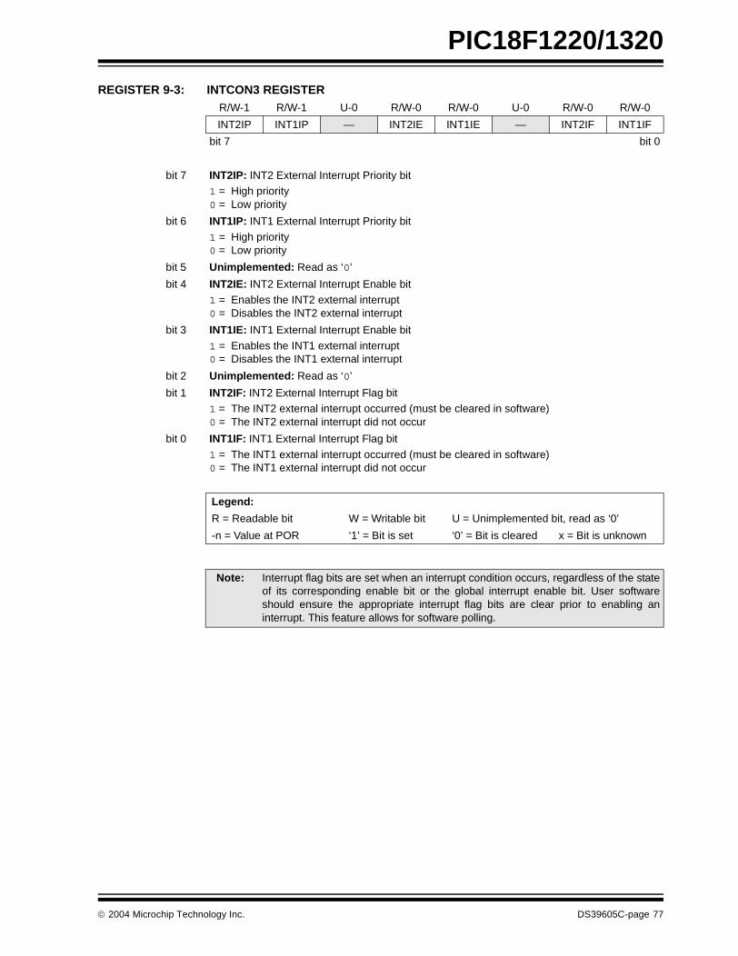
PIC18F1220/1320
REGISTER 9-3: INTCON3 REGISTER
R/W-1 R/W-1 U-0 R/W-0 R/W-0 U-0 R/W-0 R/W-0
INT2IP INT1IP — INT2IE INT1IE — INT2IF INT1IF
bit 7 bit 0
bit 7 INT2IP: INT2 External Interrupt Priority bit1 = High priority 0 = Low priority
bit 6 INT1IP: INT1 External Interrupt Priority bit
1 = High priority 0 = Low priority
bit 5 Unimplemented: Read as ‘0’
bit 4 INT2IE: INT2 External Interrupt Enable bit1 = Enables the INT2 external interrupt 0 = Disables the INT2 external interrupt
bit 3 INT1IE: INT1 External Interrupt Enable bit
1 = Enables the INT1 external interrupt 0 = Disables the INT1 external interrupt
bit 2 Unimplemented: Read as ‘0’
bit 1 INT2IF: INT2 External Interrupt Flag bit1 = The INT2 external interrupt occurred (must be cleared in software) 0 = The INT2 external interrupt did not occur
bit 0 INT1IF: INT1 External Interrupt Flag bit
1 = The INT1 external interrupt occurred (must be cleared in software) 0 = The INT1 external interrupt did not occur
Legend:
R = Readable bit W = Writable bit U = Unimplemented bit, read as ‘0’
-n = Value at POR ‘1’ = Bit is set ‘0’ = Bit is cleared x = Bit is unknown
Note: Interrupt flag bits are set when an interrupt condition occurs, regardless of the stateof its corresponding enable bit or the global interrupt enable bit. User softwareshould ensure the appropriate interrupt flag bits are clear prior to enabling aninterrupt. This feature allows for software polling.
2004 Microchip Technology Inc. DS39605C-page 77
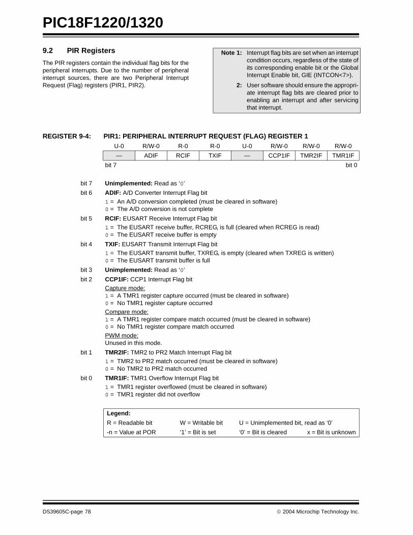
PIC18F1220/1320
9.2 PIR Registers
The PIR registers contain the individual flag bits for theperipheral interrupts. Due to the number of peripheralinterrupt sources, there are two Peripheral InterruptRequest (Flag) registers (PIR1, PIR2).
REGISTER 9-4: PIR1: PERIPHERAL INTERRUPT REQUEST (FLAG) REGISTER 1
Note 1: Interrupt flag bits are set when an interruptcondition occurs, regardless of the state ofits corresponding enable bit or the GlobalInterrupt Enable bit, GIE (INTCON<7>).
2: User software should ensure the appropri-ate interrupt flag bits are cleared prior toenabling an interrupt and after servicingthat interrupt.
U-0 R/W-0 R-0 R-0 U-0 R/W-0 R/W-0 R/W-0
— ADIF RCIF TXIF — CCP1IF TMR2IF TMR1IF
bit 7 bit 0
bit 7 Unimplemented: Read as ‘0’
bit 6 ADIF: A/D Converter Interrupt Flag bit
1 = An A/D conversion completed (must be cleared in software) 0 = The A/D conversion is not complete
bit 5 RCIF: EUSART Receive Interrupt Flag bit 1 = The EUSART receive buffer, RCREG, is full (cleared when RCREG is read) 0 = The EUSART receive buffer is empty
bit 4 TXIF: EUSART Transmit Interrupt Flag bit 1 = The EUSART transmit buffer, TXREG, is empty (cleared when TXREG is written) 0 = The EUSART transmit buffer is full
bit 3 Unimplemented: Read as ‘0’
bit 2 CCP1IF: CCP1 Interrupt Flag bit Capture mode: 1 = A TMR1 register capture occurred (must be cleared in software) 0 = No TMR1 register capture occurred Compare mode: 1 = A TMR1 register compare match occurred (must be cleared in software) 0 = No TMR1 register compare match occurred
PWM mode: Unused in this mode.
bit 1 TMR2IF: TMR2 to PR2 Match Interrupt Flag bit1 = TMR2 to PR2 match occurred (must be cleared in software) 0 = No TMR2 to PR2 match occurred
bit 0 TMR1IF: TMR1 Overflow Interrupt Flag bit 1 = TMR1 register overflowed (must be cleared in software)0 = TMR1 register did not overflow
Legend:
R = Readable bit W = Writable bit U = Unimplemented bit, read as ‘0’
-n = Value at POR ‘1’ = Bit is set ‘0’ = Bit is cleared x = Bit is unknown
DS39605C-page 78 2004 Microchip Technology Inc.

PIC18F1220/1320
REGISTER 9-5: PIR2: PERIPHERAL INTERRUPT REQUEST (FLAG) REGISTER 2 R/W-0 U-0 U-0 R/W-0 U-0 R/W-0 R/W-0 U-0
OSCFIF — — EEIF — LVDIF TMR3IF —
bit 7 bit 0
bit 7 OSCFIF: Oscillator Fail Interrupt Flag bit
1 = System oscillator failed, clock input has changed to INTOSC (must be cleared in software)0 = System clock operating
bit 6-5 Unimplemented: Read as ‘0’
bit 4 EEIF: Data EEPROM/Flash Write Operation Interrupt Flag bit1 = The write operation is complete (must be cleared in software)0 = The write operation is not complete or has not been started
bit 3 Unimplemented: Read as ‘0’
bit 2 LVDIF: Low-Voltage Detect Interrupt Flag bit 1 = A low-voltage condition occurred (must be cleared in software)0 = The device voltage is above the Low-Voltage Detect trip point
bit 1 TMR3IF: TMR3 Overflow Interrupt Flag bit1 = TMR3 register overflowed (must be cleared in software)0 = TMR3 register did not overflow
bit 0 Unimplemented: Read as ‘0’
Legend:
R = Readable bit W = Writable bit U = Unimplemented bit, read as ‘0’
-n = Value at POR ‘1’ = Bit is set ‘0’ = Bit is cleared x = Bit is unknown
2004 Microchip Technology Inc. DS39605C-page 79
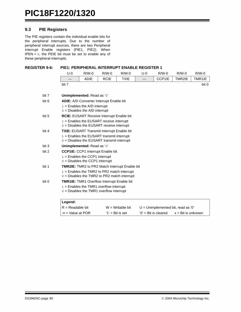
PIC18F1220/1320
9.3 PIE Registers
The PIE registers contain the individual enable bits forthe peripheral interrupts. Due to the number ofperipheral interrupt sources, there are two PeripheralInterrupt Enable registers (PIE1, PIE2). WhenIPEN = 0, the PEIE bit must be set to enable any ofthese peripheral interrupts.
REGISTER 9-6: PIE1: PERIPHERAL INTERRUPT ENABLE REGISTER 1 U-0 R/W-0 R/W-0 R/W-0 U-0 R/W-0 R/W-0 R/W-0
— ADIE RCIE TXIE — CCP1IE TMR2IE TMR1IE
bit 7 bit 0
bit 7 Unimplemented: Read as ‘0’
bit 6 ADIE: A/D Converter Interrupt Enable bit 1 = Enables the A/D interrupt 0 = Disables the A/D interrupt
bit 5 RCIE: EUSART Receive Interrupt Enable bit
1 = Enables the EUSART receive interrupt 0 = Disables the EUSART receive interrupt
bit 4 TXIE: EUSART Transmit Interrupt Enable bit 1 = Enables the EUSART transmit interrupt 0 = Disables the EUSART transmit interrupt
bit 3 Unimplemented: Read as ‘0’
bit 2 CCP1IE: CCP1 Interrupt Enable bit
1 = Enables the CCP1 interrupt 0 = Disables the CCP1 interrupt
bit 1 TMR2IE: TMR2 to PR2 Match Interrupt Enable bit1 = Enables the TMR2 to PR2 match interrupt 0 = Disables the TMR2 to PR2 match interrupt
bit 0 TMR1IE: TMR1 Overflow Interrupt Enable bit1 = Enables the TMR1 overflow interrupt 0 = Disables the TMR1 overflow interrupt
Legend:
R = Readable bit W = Writable bit U = Unimplemented bit, read as ‘0’
-n = Value at POR ‘1’ = Bit is set ‘0’ = Bit is cleared x = Bit is unknown
DS39605C-page 80 2004 Microchip Technology Inc.

PIC18F1220/1320
REGISTER 9-7: PIE2: PERIPHERAL INTERRUPT ENABLE REGISTER 2 R/W-0 U-0 U-0 R/W-0 U-0 R/W-0 R/W-0 U-0
OSCFIE — — EEIE — LVDIE TMR3IE —
bit 7 bit 0
bit 7 OSCFIE: Oscillator Fail Interrupt Enable bit1 = Enabled0 = Disabled
bit 6-5 Unimplemented: Read as ‘0’
bit 4 EEIE: Data EEPROM/Flash Write Operation Interrupt Enable bit 1 = Enabled0 = Disabled
bit 3 Unimplemented: Read as ‘0’
bit 2 LVDIE: Low-Voltage Detect Interrupt Enable bit
1 = Enabled0 = Disabled
bit 1 TMR3IE: TMR3 Overflow Interrupt Enable bit 1 = Enabled0 = Disabled
bit 0 Unimplemented: Read as ‘0’
Legend:
R = Readable bit W = Writable bit U = Unimplemented bit, read as ‘0’
-n = Value at POR ‘1’ = Bit is set ‘0’ = Bit is cleared x = Bit is unknown
2004 Microchip Technology Inc. DS39605C-page 81
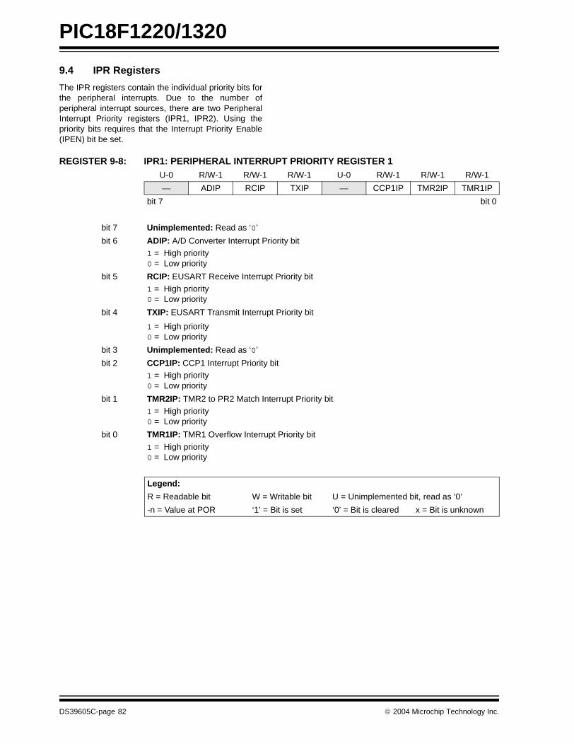
PIC18F1220/1320
9.4 IPR Registers
The IPR registers contain the individual priority bits forthe peripheral interrupts. Due to the number ofperipheral interrupt sources, there are two PeripheralInterrupt Priority registers (IPR1, IPR2). Using thepriority bits requires that the Interrupt Priority Enable(IPEN) bit be set.
REGISTER 9-8: IPR1: PERIPHERAL INTERRUPT PRIORITY REGISTER 1 U-0 R/W-1 R/W-1 R/W-1 U-0 R/W-1 R/W-1 R/W-1
— ADIP RCIP TXIP — CCP1IP TMR2IP TMR1IP
bit 7 bit 0
bit 7 Unimplemented: Read as ‘0’
bit 6 ADIP: A/D Converter Interrupt Priority bit1 = High priority 0 = Low priority
bit 5 RCIP: EUSART Receive Interrupt Priority bit
1 = High priority 0 = Low priority
bit 4 TXIP: EUSART Transmit Interrupt Priority bit
1 = High priority 0 = Low priority
bit 3 Unimplemented: Read as ‘0’
bit 2 CCP1IP: CCP1 Interrupt Priority bit1 = High priority 0 = Low priority
bit 1 TMR2IP: TMR2 to PR2 Match Interrupt Priority bit 1 = High priority 0 = Low priority
bit 0 TMR1IP: TMR1 Overflow Interrupt Priority bit
1 = High priority 0 = Low priority
Legend:
R = Readable bit W = Writable bit U = Unimplemented bit, read as ‘0’
-n = Value at POR ‘1’ = Bit is set ‘0’ = Bit is cleared x = Bit is unknown
DS39605C-page 82 2004 Microchip Technology Inc.
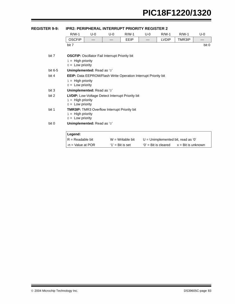
PIC18F1220/1320
REGISTER 9-9: IPR2: PERIPHERAL INTERRUPT PRIORITY REGISTER 2 R/W-1 U-0 U-0 R/W-1 U-0 R/W-1 R/W-1 U-0
OSCFIP — — EEIP — LVDIP TMR3IP —
bit 7 bit 0
bit 7 OSCFIP: Oscillator Fail Interrupt Priority bit1 = High priority0 = Low priority
bit 6-5 Unimplemented: Read as ‘0’
bit 4 EEIP: Data EEPROM/Flash Write Operation Interrupt Priority bit 1 = High priority0 = Low priority
bit 3 Unimplemented: Read as ‘0’
bit 2 LVDIP: Low-Voltage Detect Interrupt Priority bit 1 = High priority0 = Low priority
bit 1 TMR3IP: TMR3 Overflow Interrupt Priority bit 1 = High priority0 = Low priority
bit 0 Unimplemented: Read as ‘0’
Legend:
R = Readable bit W = Writable bit U = Unimplemented bit, read as ‘0’
-n = Value at POR ‘1’ = Bit is set ‘0’ = Bit is cleared x = Bit is unknown
2004 Microchip Technology Inc. DS39605C-page 83
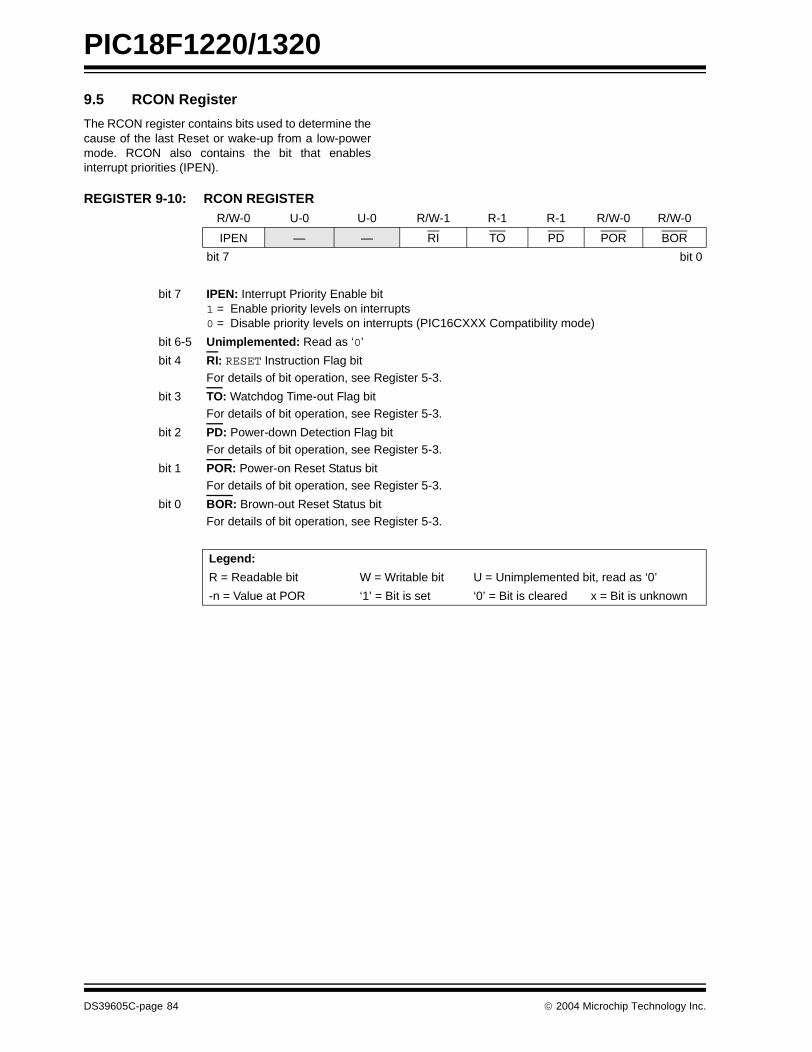
PIC18F1220/1320
9.5 RCON Register
The RCON register contains bits used to determine thecause of the last Reset or wake-up from a low-powermode. RCON also contains the bit that enablesinterrupt priorities (IPEN).
REGISTER 9-10: RCON REGISTER R/W-0 U-0 U-0 R/W-1 R-1 R-1 R/W-0 R/W-0
IPEN — — RI TO PD POR BOR
bit 7 bit 0
bit 7 IPEN: Interrupt Priority Enable bit 1 = Enable priority levels on interrupts0 = Disable priority levels on interrupts (PIC16CXXX Compatibility mode)
bit 6-5 Unimplemented: Read as ‘0’
bit 4 RI: RESET Instruction Flag bit For details of bit operation, see Register 5-3.
bit 3 TO: Watchdog Time-out Flag bit For details of bit operation, see Register 5-3.
bit 2 PD: Power-down Detection Flag bit For details of bit operation, see Register 5-3.
bit 1 POR: Power-on Reset Status bitFor details of bit operation, see Register 5-3.
bit 0 BOR: Brown-out Reset Status bit For details of bit operation, see Register 5-3.
Legend:
R = Readable bit W = Writable bit U = Unimplemented bit, read as ‘0’
-n = Value at POR ‘1’ = Bit is set ‘0’ = Bit is cleared x = Bit is unknown
DS39605C-page 84 2004 Microchip Technology Inc.
PIC18F1220/1320
9.6 INTn Pin Interrupts
External interrupts on the RB0/INT0, RB1/INT1 andRB2/INT2 pins are edge-triggered: either rising if thecorresponding INTEDGx bit is set in the INTCON2 reg-ister, or falling if the INTEDGx bit is clear. When a validedge appears on the RBx/INTx pin, the correspondingflag bit, INTxF, is set. This interrupt can be disabled byclearing the corresponding enable bit, INTxE. Flag bit,INTxF, must be cleared in software in the InterruptService Routine before re-enabling the interrupt. Allexternal interrupts (INT0, INT1 and INT2) can wake-upthe processor from low-power modes if bit INTxE wasset prior to going into low-power modes. If the GlobalInterrupt Enable bit, GIE, is set, the processor willbranch to the interrupt vector following wake-up.
Interrupt priority for INT1 and INT2 is determined by thevalue contained in the interrupt priority bits, INT1IP(INTCON3<6>) and INT2IP (INTCON3<7>). There isno priority bit associated with INT0. It is always a highpriority interrupt source.
9.7 TMR0 Interrupt
In 8-bit mode (which is the default), an overflow(FFh → 00h) in the TMR0 register will set flag bit,TMR0IF. In 16-bit mode, an overflow (FFFFh → 0000h)in the TMR0H:TMR0L registers will set flag bit,TMR0IF. The interrupt can be enabled/disabled bysetting/clearing enable bit, TMR0IE (INTCON<5>).Interrupt priority for Timer0 is determined by the valuecontained in the interrupt priority bit, TMR0IP(INTCON2<2>). See Section 11.0 “Timer0 Module”for further details on the Timer0 module.
9.8 PORTB Interrupt-on-Change
An input change on PORTB<7:4> sets flag bit, RBIF(INTCON<0>). The interrupt can be enabled/disabledby setting/clearing enable bit, RBIE (INTCON<3>).Interrupt priority for PORTB interrupt-on-change isdetermined by the value contained in the interruptpriority bit, RBIP (INTCON2<0>).
9.9 Context Saving During Interrupts
During interrupts, the return PC address is saved on thestack. Additionally, the WREG, Status and BSR registersare saved on the fast return stack. If a fast return frominterrupt is not used (see Section 5.3 “Fast RegisterStack”), the user may need to save the WREG, Statusand BSR registers on entry to the Interrupt ServiceRoutine. Depending on the user’s application, otherregisters may also need to be saved. Example 9-1saves and restores the WREG, Status and BSRregisters during an Interrupt Service Routine.
EXAMPLE 9-1: SAVING STATUS, WREG AND BSR REGISTERS IN RAM
MOVWF W_TEMP ; W_TEMP is in virtual bankMOVFF STATUS, STATUS_TEMP ; STATUS_TEMP located anywhereMOVFF BSR, BSR_TEMP ; BSR_TMEP located anywhere;; USER ISR CODE;MOVFF BSR_TEMP, BSR ; Restore BSRMOVF W_TEMP, W ; Restore WREGMOVFF STATUS_TEMP, STATUS ; Restore STATUS
2004 Microchip Technology Inc. DS39605C-page 85

PIC18F1220/1320
NOTES:
DS39605C-page 86 2004 Microchip Technology Inc.

PIC18F1220/1320
10.0 I/O PORTS
Depending on the device selected and featuresenabled, there are up to five ports available. Some pinsof the I/O ports are multiplexed with an alternatefunction from the peripheral features on the device. Ingeneral, when a peripheral is enabled, that pin may notbe used as a general purpose I/O pin.
Each port has three registers for its operation. Theseregisters are:
• TRIS register (data direction register)
• PORT register (reads the levels on the pins of the device)
• LAT register (output latch)
The Data Latch (LATA) register is useful for read-modify-write operations on the value that the I/O pinsare driving.
A simplified model of a generic I/O port without theinterfaces to other peripherals is shown in Figure 10-1.
FIGURE 10-1: GENERIC I/O PORT OPERATION
10.1 PORTA, TRISA and LATA Registers
PORTA is an 8-bit wide, bidirectional port. The corre-sponding data direction register is TRISA. Setting aTRISA bit (= 1) will make the corresponding PORTA pinan input (i.e., put the corresponding output driver in ahigh-impedance mode). Clearing a TRISA bit (= 0) willmake the corresponding PORTA pin an output (i.e., putthe contents of the output latch on the selected pin).
Reading the PORTA register reads the status of thepins, whereas writing to it will write to the port latch.
The Data Latch register (LATA) is also memorymapped. Read-modify-write operations on the LATAregister read and write the latched output value forPORTA.
The RA4 pin is multiplexed with the Timer0 moduleclock input to become the RA4/T0CKI pin.
The sixth pin of PORTA (MCLR/VPP/RA5) is an inputonly pin. Its operation is controlled by the MCLREconfiguration bit in Configuration Register 3H(CONFIG3H<7>). When selected as a port pin(MCLRE = 0), it functions as a digital input only pin; assuch, it does not have TRIS or LAT bits associated withits operation. Otherwise, it functions as the device’sMaster Clear input. In either configuration, RA5 alsofunctions as the programming voltage input duringprogramming.
Pins RA6 and RA7 are multiplexed with the main oscil-lator pins; they are enabled as oscillator or I/O pins bythe selection of the main oscillator in ConfigurationRegister 1H (see Section 19.1 “Configuration Bits”for details). When they are not used as port pins, RA6and RA7 and their associated TRIS and LAT bits areread as ‘0’.
The other PORTA pins are multiplexed with analoginputs, the analog VREF+ and VREF- inputs and the LVDinput. The operation of pins RA3:RA0 as A/D converterinputs is selected by clearing/setting the control bits inthe ADCON1 register (A/D Control Register 1).
The RA4/T0CKI pin is a Schmitt Trigger input and anopen-drain output. All other PORTA pins have TTLinput levels and full CMOS output drivers.
The TRISA register controls the direction of the RApins, even when they are being used as analog inputs.The user must ensure the bits in the TRISA register aremaintained set when using them as analog inputs.
EXAMPLE 10-1: INITIALIZING PORTA
DataBus
WR LAT
WR TRIS
RD Port
Data Latch
TRIS Latch
RD TRIS
InputBuffer
I/O pin(1)
QD
CK
QD
CK
EN
Q D
EN
RD LAT
or Port
Note 1: I/O pins have diode protection to VDD and VSS.
Note: On a Power-on Reset, RA5 is enabled as adigital input only if Master Clear functionalityis disabled.
Note: On a Power-on Reset, RA3:RA0 areconfigured as analog inputs and read as‘0’. RA4 is always a digital pin.
CLRF PORTA ; Initialize PORTA by; clearing output; data latches
CLRF LATA ; Alternate method; to clear output; data latches
MOVLW 0x7F ; Configure A/D MOVWF ADCON1 ; for digital inputsMOVLW 0xD0 ; Value used to
; initialize data ; direction
MOVWF TRISA ; Set RA<3:0> as outputs; RA<7:4> as inputs
2004 Microchip Technology Inc. DS39605C-page 87
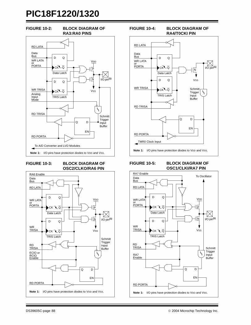
PIC18F1220/1320
FIGURE 10-2: BLOCK DIAGRAM OFRA3:RA0 PINS
FIGURE 10-3: BLOCK DIAGRAM OF OSC2/CLKO/RA6 PIN
FIGURE 10-4: BLOCK DIAGRAM OF RA4/T0CKI PIN
FIGURE 10-5: BLOCK DIAGRAM OF OSC1/CLKI/RA7 PIN
DataBus
Q D
EN
P
N
WR LATA
WR TRISA
Data Latch
TRIS Latch
RD TRISA
RD PORTA
VSS
VDD
I/O pin(1)
Note 1: I/O pins have protection diodes to VDD and VSS.
AnalogInputMode
To A/D Converter and LVD Modules
RD LATA
orPORTA
QD
QCK
QD
QCK
SchmittTriggerInputBuffer
DataBus
QD
QCK
Q D
EN
P
N
WR LATA
WR
Data Latch
TRIS Latch
RD
RD PORTA
VSS
VDD
I/O pin(1)
Note 1: I/O pins have protection diodes to VDD and VSS.
orPORTA
RD LATA
RA6 Enable
ECIO or
EnableRCIO
TRISA
QD
QCK
TRISA
SchmittTriggerInputBuffer
DataBus
WR TRISA
RD PORTA
Data Latch
TRIS Latch
SchmittTriggerInputBuffer
N
VSS
I/O pin(1)
TMR0 Clock Input
QD
QCK
QD
QCK
EN
Q D
EN
RD LATA
WR LATAorPORTA
Note 1: I/O pins have protection diodes to VDD and VSS.
RD TRISA
DataBus
QD
QCK
Q D
EN
P
N
WR LATA
WR
Data Latch
TRIS Latch
RD
RD PORTA
VSS
VDD
I/O pin(1)
Note 1: I/O pins have protection diodes to VDD and VSS.
orPORTA
RD LATA
EnableRA7
TRISA
QD
QCK
TRISA
RA7 EnableTo Oscillator
SchmittTriggerInputBuffer
DS39605C-page 88 2004 Microchip Technology Inc.
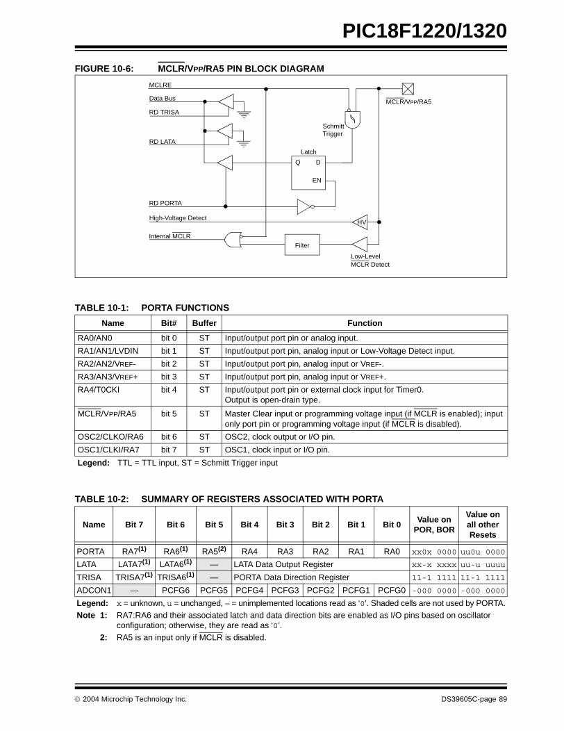
PIC18F1220/1320
FIGURE 10-6: MCLR/VPP/RA5 PIN BLOCK DIAGRAM
TABLE 10-1: PORTA FUNCTIONS
TABLE 10-2: SUMMARY OF REGISTERS ASSOCIATED WITH PORTA
MCLR/VPP/RA5Data Bus
RD PORTA
RD LATA
SchmittTrigger
MCLRE
RD TRISA
Q D
EN
Latch
Filter
Low-LevelMCLR Detect
High-Voltage Detect
Internal MCLR
HV
Name Bit# Buffer Function
RA0/AN0 bit 0 ST Input/output port pin or analog input.
RA1/AN1/LVDIN bit 1 ST Input/output port pin, analog input or Low-Voltage Detect input.
RA2/AN2/VREF- bit 2 ST Input/output port pin, analog input or VREF-.
RA3/AN3/VREF+ bit 3 ST Input/output port pin, analog input or VREF+.
RA4/T0CKI bit 4 ST Input/output port pin or external clock input for Timer0. Output is open-drain type.
MCLR/VPP/RA5 bit 5 ST Master Clear input or programming voltage input (if MCLR is enabled); input only port pin or programming voltage input (if MCLR is disabled).
OSC2/CLKO/RA6 bit 6 ST OSC2, clock output or I/O pin.
OSC1/CLKI/RA7 bit 7 ST OSC1, clock input or I/O pin.
Legend: TTL = TTL input, ST = Schmitt Trigger input
Name Bit 7 Bit 6 Bit 5 Bit 4 Bit 3 Bit 2 Bit 1 Bit 0Value on
POR, BOR
Value on all other Resets
PORTA RA7(1) RA6(1) RA5(2) RA4 RA3 RA2 RA1 RA0 xx0x 0000 uu0u 0000
LATA LATA7(1) LATA6(1) — LATA Data Output Register xx-x xxxx uu-u uuuu
TRISA TRISA7(1) TRISA6(1) — PORTA Data Direction Register 11-1 1111 11-1 1111
ADCON1 — PCFG6 PCFG5 PCFG4 PCFG3 PCFG2 PCFG1 PCFG0 -000 0000 -000 0000
Legend: x = unknown, u = unchanged, – = unimplemented locations read as ‘0’. Shaded cells are not used by PORTA.
Note 1: RA7:RA6 and their associated latch and data direction bits are enabled as I/O pins based on oscillator configuration; otherwise, they are read as ‘0’.
2: RA5 is an input only if MCLR is disabled.
2004 Microchip Technology Inc. DS39605C-page 89
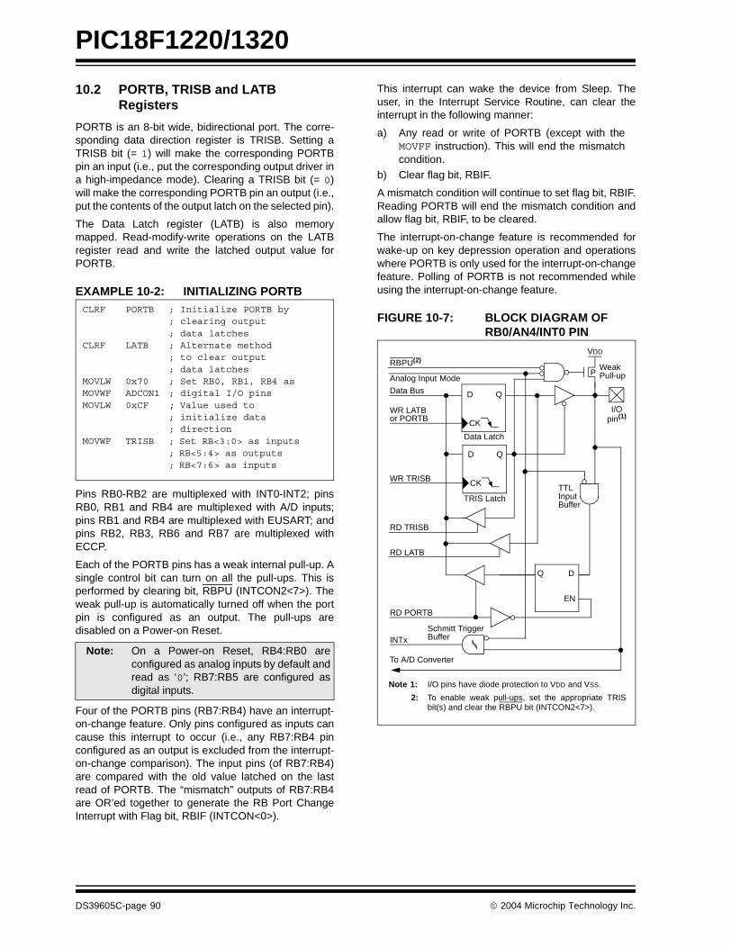
PIC18F1220/1320
10.2 PORTB, TRISB and LATB Registers
PORTB is an 8-bit wide, bidirectional port. The corre-sponding data direction register is TRISB. Setting aTRISB bit (= 1) will make the corresponding PORTBpin an input (i.e., put the corresponding output driver ina high-impedance mode). Clearing a TRISB bit (= 0)will make the corresponding PORTB pin an output (i.e.,put the contents of the output latch on the selected pin).
The Data Latch register (LATB) is also memorymapped. Read-modify-write operations on the LATBregister read and write the latched output value forPORTB.
EXAMPLE 10-2: INITIALIZING PORTB
Pins RB0-RB2 are multiplexed with INT0-INT2; pinsRB0, RB1 and RB4 are multiplexed with A/D inputs;pins RB1 and RB4 are multiplexed with EUSART; andpins RB2, RB3, RB6 and RB7 are multiplexed withECCP.
Each of the PORTB pins has a weak internal pull-up. Asingle control bit can turn on all the pull-ups. This isperformed by clearing bit, RBPU (INTCON2<7>). Theweak pull-up is automatically turned off when the portpin is configured as an output. The pull-ups aredisabled on a Power-on Reset.
Four of the PORTB pins (RB7:RB4) have an interrupt-on-change feature. Only pins configured as inputs cancause this interrupt to occur (i.e., any RB7:RB4 pinconfigured as an output is excluded from the interrupt-on-change comparison). The input pins (of RB7:RB4)are compared with the old value latched on the lastread of PORTB. The “mismatch” outputs of RB7:RB4are OR’ed together to generate the RB Port ChangeInterrupt with Flag bit, RBIF (INTCON<0>).
This interrupt can wake the device from Sleep. Theuser, in the Interrupt Service Routine, can clear theinterrupt in the following manner:
a) Any read or write of PORTB (except with theMOVFF instruction). This will end the mismatchcondition.
b) Clear flag bit, RBIF.
A mismatch condition will continue to set flag bit, RBIF.Reading PORTB will end the mismatch condition andallow flag bit, RBIF, to be cleared.
The interrupt-on-change feature is recommended forwake-up on key depression operation and operationswhere PORTB is only used for the interrupt-on-changefeature. Polling of PORTB is not recommended whileusing the interrupt-on-change feature.
FIGURE 10-7: BLOCK DIAGRAM OF RB0/AN4/INT0 PIN
Note: On a Power-on Reset, RB4:RB0 areconfigured as analog inputs by default andread as ‘0’; RB7:RB5 are configured asdigital inputs.
CLRF PORTB ; Initialize PORTB by; clearing output; data latches
CLRF LATB ; Alternate method; to clear output; data latches
MOVLW 0x70 ; Set RB0, RB1, RB4 asMOVWF ADCON1 ; digital I/O pinsMOVLW 0xCF ; Value used to
; initialize data ; direction
MOVWF TRISB ; Set RB<3:0> as inputs; RB<5:4> as outputs; RB<7:6> as inputs
Data Latch
RBPU(2)
P
VDD
Data Bus
WR LATB
WR TRISB
RD TRISB
RD PORTB
WeakPull-up
INTx
I/Opin(1)
Schmitt TriggerBuffer
TRIS Latch
RD LATB
or PORTB
Note 1: I/O pins have diode protection to VDD and VSS.
2: To enable weak pull-ups, set the appropriate TRISbit(s) and clear the RBPU bit (INTCON2<7>).
To A/D Converter
Analog Input Mode
TTLInputBuffer
QD
CK
QD
CK
EN
Q D
EN
DS39605C-page 90 2004 Microchip Technology Inc.

PIC18F1220/1320
FIGURE 10-8: BLOCK DIAGRAM OF RB1/AN5/TX/CK/INT1 PIN
Data Latch
RBPU(2)
P
VDD
QD
CK
QD
CK
Q D
EN
Data Bus
WR LATB
WR TRISB
RD TRISB
RD PORTB
WeakPull-up
RD PORTB
RB1 pin(1)
TRIS Latch
RD LATB
orPORTB
Note 1: I/O pins have diode protection to VDD and VSS.
2: To enable weak pull-ups, set the appropriate TRIS bit(s) and clear the RBPU bit (INTCON2<7>).
To A/D Converter
INT1/CK Input
Analog InputMode
1
0
TX/CK Data
EUSART Enable
SchmittTriggerInputBuffer
TX/CK TRIS
Analog Input Mode
TTLInputBuffer
2004 Microchip Technology Inc. DS39605C-page 91

PIC18F1220/1320
FIGURE 10-9: BLOCK DIAGRAM OF RB2/P1B/INT2 PIN
Data Latch
RBPU(2)
P
VDD
QD
CK
QD
CK
Q D
EN
Data Bus
WR LATB or
WR TRISB
RD TRISB
RD PORTB
WeakPull-up
RD PORTB
RB2 pin(1)
TTLInputBuffer
TRIS Latch
RD LATB
PORTB
P1B Data1
0
Note 1: I/O pins have diode protection to VDD and VSS.
2: To enable weak pull-ups, set the appropriate TRIS bit(s) and clear the RBPU bit (INTCON2<7>).
P1B Enable
INT2 Input
SchmittTrigger
P1B/D Tri-StateAuto-Shutdown
DS39605C-page 92 2004 Microchip Technology Inc.
PIC18F1220/1320
FIGURE 10-10: BLOCK DIAGRAM OF RB3/CCP1/P1A PIN
Data Bus
WR LATB or
WR TRISB
Data Latch
TRIS Latch
RD TRISB
QD
QCK
Q D
EN
ECCP1/P1A Data Out1
0
QD
QCK
P
N
VDD
VSS
RD PORTB
ECCP1 Input
RB3 pinPORTB
RD LATB
SchmittTrigger
VDD
WeakPull-upP
RBPU(2)
TTL InputBuffer
Note 1: I/O pins have diode protection to VDD and VSS.
2: To enable weak pull-ups, set the appropriate TRIS bit(s) and clear the RBPU bit (INTCON2<7>).
3: ECCP1 pin output enable active for any PWM mode and Compare mode, where CCP1M<3:0> = 1000 or 1001.
4: ECCP1 pin input enable active for Capture mode only.
ECCP1(3) pin Output Enable
P1A/C Tri-State Auto-Shutdown
ECCP1(4) pin Input Enable
2004 Microchip Technology Inc. DS39605C-page 93

PIC18F1220/1320
FIGURE 10-11: BLOCK DIAGRAM OF RB4/AN6/RX/DT/KBI0 PIN
Data Bus
WR LATB or
WR TRISB
Data Latch
TRIS Latch
RD TRISB
QD
QCK
Q D
EN
DT Data1
0
QD
QCK
RD PORTB
RB4 pinPORTB
RD LATB
RBPU(2)
P WeakPull-up
Q1
From other Q D
EN
Set RBIF
RB7:RB4 pins RD PORTB
Q3
To A/D Converter
EUSART Enabled
TTLInputBuffer
Note 1: I/O pins have diode protection to VDD and VSS.
2: To enable weak pull-ups, set the appropriate TRIS bit(s) and clear the RBPU bit (INTCON2<7>).
DT TRIS
Analog Input Mode
RX/DT Input
Analog InputMode
SchmittTrigger
VDD
DS39605C-page 94 2004 Microchip Technology Inc.
PIC18F1220/1320
FIGURE 10-12: BLOCK DIAGRAM OF RB5/PGM/KBI1 PIN
Data Latch
From other
RBPU(2)
P
VDD
I/O pin(1)QD
CK
QD
CK
Q D
EN
Q D
EN
Data Bus
WR LATB
WR TRISB
Set RBIF
TRIS Latch
RD TRISB
RD PORTB
RB7:RB5 and
WeakPull-up
RD PORTB
Latch
TTLInputBuffer ST
Buffer
RB7:RB5 in Serial Programming Mode
Q3
Q1
RD LATB
or PORTB
Note 1: I/O pins have diode protection to VDD and VSS.
2: To enable weak pull-ups, set the appropriate TRIS bit(s) and clear the RBPU bit(INTCON2<7>).
RB4 pins
2004 Microchip Technology Inc. DS39605C-page 95
PIC18F1220/1320
FIGURE 10-13: BLOCK DIAGRAM OF RB6/PGC/T1OSO/T13CKI/P1C/KBI2 PIN
Data Bus
WR LATB or
WR TRISB
Data Latch
TRIS Latch
RD TRISB
QD
QCK
Q D
EN
P1C Data1
0
QD
QCK
RD PORTB
RB6 pinPORTB
RD LATB
SchmittTrigger
RBPU(2)
P WeakPull-up
Q1
From other Q D
EN
Set RBIF
RB7:RB4 pins RD PORTB
Q3
PGC
From RB7 pin
Timer1Oscillator
T1OSCEN
T13CKI
Note 1: I/O pins have diode protection to VDD and VSS.
2: To enable weak pull-ups, set the appropriate TRIS bit(s) and clear the RBPU bit (INTCON2<7>).
TTLBuffer
ECCP1 P1C/D Enable
P1B/D Tri-State Auto-Shutdown
VDD
DS39605C-page 96 2004 Microchip Technology Inc.

PIC18F1220/1320
FIGURE 10-14: BLOCK DIAGRAM OF RB7/PGD/T1OSI/P1D/KBI3 PIN
Data Bus
WR LATB or
WR TRISB
Data Latch
TRIS Latch
RD TRISB
QD
QCK
Q D
EN
P1D Data1
0
QD
QCK
RD PORTB
RB7 pinPORTB
RD LATB
SchmittTrigger
To RB6 pin
RBPU(2)
P WeakPull-up
Q1
From other Q D
EN
Set RBIF
RB7:RB4 pins RD PORTB
Q3
PGD
ECCP1 P1C/D Enable
TTLInputBuffer
Note 1: I/O pins have diode protection to VDD and VSS.
2: To enable weak pull-ups, set the appropriate TRIS bit(s) and clear the RBPU bit (INTCON2<7>).
P1B/D Tri-State Auto-Shutdown
T1OSCEN
VDD
2004 Microchip Technology Inc. DS39605C-page 97
PIC18F1220/1320
TABLE 10-3: PORTB FUNCTIONS
TABLE 10-4: SUMMARY OF REGISTERS ASSOCIATED WITH PORTB
Name Bit# Buffer Function
RB0/AN4/INT0 bit 0 TTL(1)/ST(2) Input/output port pin, analog input or external interrupt input 0.
RB1/AN5/TX/CK/INT1 bit 1 TTL(1)/ST(2) Input/output port pin, analog input, Enhanced USART Asynchronous Transmit, Addressable USART Synchronous Clock or external interrupt input 1.
RB2/P1B/INT2 bit 2 TTL(1)/ST(2) Input/output port pin or external interrupt input 2.Internal software programmable weak pull-up.
RB3/CCP1/P1A bit 3 TTL(1)/ST(3) Input/output port pin or Capture1 input/Compare1 output/PWM output. Internal software programmable weak pull-up.
RB4/AN6/RX/DT/KBI0 bit 4 TTL(1)/ST(4) Input/output port pin (with interrupt-on-change), analog input, Enhanced USART Asynchronous Receive or Addressable USART Synchronous Data.
RB5/PGM/KBI1 bit 5 TTL(1)/ST(5) Input/output port pin (with interrupt-on-change). Internal software programmable weak pull-up.Low-Voltage ICSP enable pin.
RB6/PGC/T1OSO/T13CKI/P1C/KBI2
bit 6 TTL(1)/ST(5,6) Input/output port pin (with interrupt-on-change), Timer1/Timer3 clock input or Timer1oscillator output. Internal software programmable weak pull-up. Serial programming clock.
RB7/PGD/T1OSI/P1D/KBI3 bit 7 TTL(1)/ST(5) Input/output port pin (with interrupt-on-change) or Timer1 oscillator input. Internal software programmable weak pull-up. Serial programming data.
Legend: TTL = TTL input, ST = Schmitt Trigger input
Note 1: This buffer is a TTL input when configured as a port input pin.2: This buffer is a Schmitt Trigger input when configured as the external interrupt.3: This buffer is a Schmitt Trigger input when configured as the CCP1 input.
4: This buffer is a Schmitt Trigger input when used as EUSART receive input.5: This buffer is a Schmitt Trigger input when used in Serial Programming mode.6: This buffer is a TTL input when used as the T13CKI input.
Name Bit 7 Bit 6 Bit 5 Bit 4 Bit 3 Bit 2 Bit 1 Bit 0Value on
POR, BOR
Value on all other Resets
PORTB RB7 RB6 RB5 RB4 RB3 RB2 RB1 RB0 xxxq qqqq uuuu uuuu
LATB LATB Data Output Register xxxx xxxx uuuu uuuu
TRISB PORTB Data Direction Register 1111 1111 1111 1111
INTCON GIE/GIEH PEIE/GIEL TMR0IE INT0IE RBIE TMR0IF INT0IF RBIF 0000 000x 0000 000u
INTCON2 RBPU INTEDG0 INTEDG1 INTEDG2 — TMR0IP — RBIP 1111 -1-1 1111 -1-1
INTCON3 INT2IP INT1IP — INT2IE INT1IE — INT2IF INT1IF 11-0 0-00 11-0 0-00
ADCON1 — PCFG6 PCFG5 PCFG4 PCFG3 PCFG2 PCFG1 PCFG0 -000 0000 -000 0000
Legend: x = unknown, u = unchanged, q = value depends on condition. Shaded cells are not used by PORTB.
DS39605C-page 98 2004 Microchip Technology Inc.

PIC18F1220/1320
11.0 TIMER0 MODULE
The Timer0 module has the following features:
• Software selectable as an 8-bit or 16-bit timer/counter
• Readable and writable• Dedicated 8-bit software programmable prescaler• Clock source selectable to be external or internal
• Interrupt-on-overflow from FFh to 00h in 8-bit mode and FFFFh to 0000h in 16-bit mode
• Edge select for external clock
Figure 11-1 shows a simplified block diagram of theTimer0 module in 8-bit mode and Figure 11-2 shows asimplified block diagram of the Timer0 module in 16-bitmode.
The T0CON register (Register 11-1) is a readable andwritable register that controls all the aspects of Timer0,including the prescale selection.
REGISTER 11-1: T0CON: TIMER0 CONTROL REGISTER R/W-1 R/W-1 R/W-1 R/W-1 R/W-1 R/W-1 R/W-1 R/W-1
TMR0ON T08BIT T0CS T0SE PSA T0PS2 T0PS1 T0PS0
bit 7 bit 0
bit 7 TMR0ON: Timer0 On/Off Control bit 1 = Enables Timer0 0 = Stops Timer0
bit 6 T08BIT: Timer0 8-bit/16-bit Control bit 1 = Timer0 is configured as an 8-bit timer/counter 0 = Timer0 is configured as a 16-bit timer/counter
bit 5 T0CS: Timer0 Clock Source Select bit
1 = Transition on T0CKI pin 0 = Internal instruction cycle clock (CLKO)
bit 4 T0SE: Timer0 Source Edge Select bit1 = Increment on high-to-low transition on T0CKI pin 0 = Increment on low-to-high transition on T0CKI pin
bit 3 PSA: Timer0 Prescaler Assignment bit 1 = TImer0 prescaler is NOT assigned. Timer0 clock input bypasses prescaler. 0 = Timer0 prescaler is assigned. Timer0 clock input comes from prescaler output.
bit 2-0 T0PS2:T0PS0: Timer0 Prescaler Select bits
111 = 1:256 Prescale value110 = 1:128 Prescale value101 = 1:64 Prescale value100 = 1:32 Prescale value011 = 1:16 Prescale value010 = 1:8 Prescale value001 = 1:4 Prescale value000 = 1:2 Prescale value
Legend:
R = Readable bit W = Writable bit U = Unimplemented bit, read as ‘0’
-n = Value at POR ‘1’ = Bit is set ‘0’ = Bit is cleared x = Bit is unknown
2004 Microchip Technology Inc. DS39605C-page 99
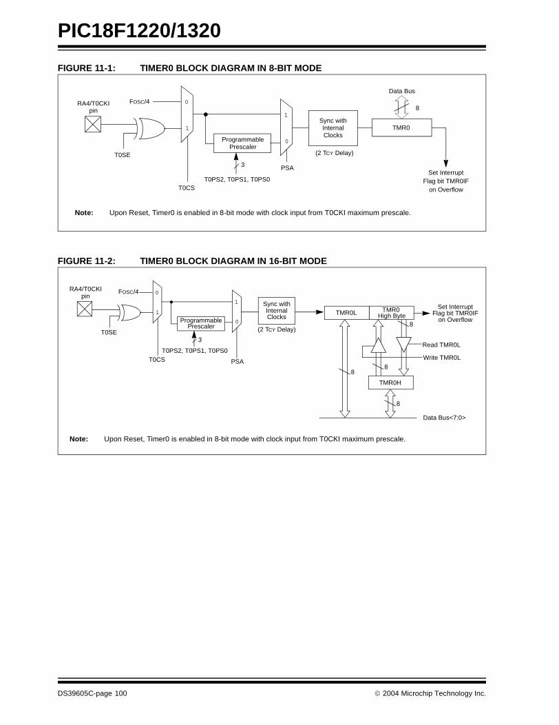
PIC18F1220/1320
FIGURE 11-1: TIMER0 BLOCK DIAGRAM IN 8-BIT MODE
FIGURE 11-2: TIMER0 BLOCK DIAGRAM IN 16-BIT MODE
Note: Upon Reset, Timer0 is enabled in 8-bit mode with clock input from T0CKI maximum prescale.
RA4/T0CKI
T0SE
0
1
1
0
T0CS
FOSC/4
ProgrammablePrescaler
Sync withInternalClocks
TMR0
(2 TCY Delay)
Data Bus
8
PSA
T0PS2, T0PS1, T0PS0Set Interrupt
Flag bit TMR0IFon Overflow
3
pin
Note: Upon Reset, Timer0 is enabled in 8-bit mode with clock input from T0CKI maximum prescale.
T0SE
0
1
1
0
T0CS
FOSC/4
ProgrammablePrescaler
Sync withInternalClocks
TMR0L
(2 TCY Delay)
Data Bus<7:0>
8
PSA
T0PS2, T0PS1, T0PS0
Set InterruptFlag bit TMR0IF
on Overflow
3
TMR0
TMR0H
High Byte
88
8
Read TMR0L
Write TMR0L
RA4/T0CKIpin
DS39605C-page 100 2004 Microchip Technology Inc.
PIC18F1220/1320
11.1 Timer0 Operation
Timer0 can operate as a timer or as a counter.
Timer mode is selected by clearing the T0CS bit. InTimer mode, the Timer0 module will increment everyinstruction cycle (without prescaler). If the TMR0 regis-ter is written, the increment is inhibited for the followingtwo instruction cycles. The user can work around thisby writing an adjusted value to the TMR0 register.
Counter mode is selected by setting the T0CS bit. InCounter mode, Timer0 will increment either on everyrising or falling edge of pin RA4/T0CKI. The increment-ing edge is determined by the Timer0 Source EdgeSelect bit (T0SE). Clearing the T0SE bit selects therising edge.
When an external clock input is used for Timer0, it mustmeet certain requirements. The requirements ensurethe external clock can be synchronized with the internalphase clock (TOSC). Also, there is a delay in the actualincrementing of Timer0 after synchronization.
11.2 Prescaler
An 8-bit counter is available as a prescaler for the Timer0module. The prescaler is not readable or writable.
The PSA and T0PS2:T0PS0 bits determine theprescaler assignment and prescale ratio.
Clearing bit PSA will assign the prescaler to the Timer0module. When the prescaler is assigned to the Timer0module, prescale values of 1:2, 1:4, ..., 1:256 areselectable.
When assigned to the Timer0 module, all instructionswriting to the TMR0 register (e.g., CLRF TMR0, MOVWFTMR0, BSF TMR0, x, ..., etc.) will clear the prescalercount.
11.2.1 SWITCHING PRESCALER ASSIGNMENT
The prescaler assignment is fully under softwarecontrol (i.e., it can be changed “on-the-fly” duringprogram execution).
11.3 Timer0 Interrupt
The TMR0 interrupt is generated when the TMR0 reg-ister overflows from FFh to 00h in 8-bit mode, or FFFFhto 0000h in 16-bit mode. This overflow sets the TMR0IFbit. The interrupt can be masked by clearing theTMR0IE bit. The TMR0IF bit must be cleared in soft-ware by the Timer0 module Interrupt Service Routinebefore re-enabling this interrupt. The TMR0 interruptcannot awaken the processor from Low-Power Sleepmode, since the timer requires clock cycles even whenT0CS is set.
11.4 16-Bit Mode Timer Reads and Writes
TMR0H is not the high byte of the timer/counter in16-bit mode, but is actually a buffered version of thehigh byte of Timer0 (refer to Figure 11-2). The high byteof the Timer0 counter/timer is not directly readable norwritable. TMR0H is updated with the contents of thehigh byte of Timer0 during a read of TMR0L. This pro-vides the ability to read all 16 bits of Timer0, withouthaving to verify that the read of the high and low bytewere valid due to a rollover between successive readsof the high and low byte.
A write to the high byte of Timer0 must also take placethrough the TMR0H Buffer register. Timer0 high byte isupdated with the contents of TMR0H when a writeoccurs to TMR0L. This allows all 16 bits of Timer0 to beupdated at once.
TABLE 11-1: REGISTERS ASSOCIATED WITH TIMER0
Note: Writing to TMR0 when the prescaler isassigned to Timer0 will clear the prescalercount, but will not change the prescalerassignment.
Name Bit 7 Bit 6 Bit 5 Bit 4 Bit 3 Bit 2 Bit 1 Bit 0Value on
POR, BOR
Value on all other Resets
TMR0L Timer0 Module Low Byte Register xxxx xxxx uuuu uuuu
TMR0H Timer0 Module High Byte Register 0000 0000 0000 0000
INTCON GIE/GIEH PEIE/GIEL TMR0IE INT0IE RBIE TMR0IF INT0IF RBIF 0000 000x 0000 000u
T0CON TMR0ON T08BIT T0CS T0SE PSA T0PS2 T0PS1 T0PS0 1111 1111 1111 1111
TRISA RA7(1) RA6(1) — PORTA Data Direction Register 11-1 1111 11-1 1111
Legend: x = unknown, u = unchanged, – = unimplemented locations read as ‘0’. Shaded cells are not used by Timer0.Note 1: RA6 and RA7 are enabled as I/O pins, depending on the oscillator mode selected in Configuration Word 1H.
2004 Microchip Technology Inc. DS39605C-page 101

PIC18F1220/1320
NOTES:
DS39605C-page 102 2004 Microchip Technology Inc.

PIC18F1220/1320
12.0 TIMER1 MODULE
The Timer1 module timer/counter has the followingfeatures:
• 16-bit timer/counter(two 8-bit registers: TMR1H and TMR1L)
• Readable and writable (both registers)
• Internal or external clock select• Interrupt-on-overflow from FFFFh to 0000h• Reset from CCP module special event trigger
• Status of system clock operation
Figure 12-1 is a simplified block diagram of the Timer1module.
Register 12-1 details the Timer1 Control register. Thisregister controls the operating mode of the Timer1module and contains the Timer1 Oscillator Enable bit(T1OSCEN). Timer1 can be enabled or disabled bysetting or clearing control bit, TMR1ON (T1CON<0>).
The Timer1 oscillator can be used as a secondary clocksource in power managed modes. When the T1RUN bitis set, the Timer1 oscillator is providing the systemclock. If the Fail-Safe Clock Monitor is enabled and theTimer1 oscillator fails while providing the system clock,polling the T1RUN bit will indicate whether the clock isbeing provided by the Timer1 oscillator or anothersource.
Timer1 can also be used to provide Real-Time Clock(RTC) functionality to applications, with only a minimaladdition of external components and code overhead.
REGISTER 12-1: T1CON: TIMER1 CONTROL REGISTER R/W-0 R-0 R/W-0 R/W-0 R/W-0 R/W-0 R/W-0 R/W-0
RD16 T1RUN T1CKPS1 T1CKPS0 T1OSCEN T1SYNC TMR1CS TMR1ON
bit 7 bit 0
bit 7 RD16: 16-bit Read/Write Mode Enable bit1 = Enables register read/write of TImer1 in one 16-bit operation0 = Enables register read/write of Timer1 in two 8-bit operations
bit 6 T1RUN: Timer1 System Clock Status bit
1 = System clock is derived from Timer1 oscillator0 = System clock is derived from another source
bit 5-4 T1CKPS1:T1CKPS0: Timer1 Input Clock Prescale Select bits11 = 1:8 Prescale value 10 = 1:4 Prescale value 01 = 1:2 Prescale value 00 = 1:1 Prescale value
bit 3 T1OSCEN: Timer1 Oscillator Enable bit1 = Timer1 oscillator is enabled 0 = Timer1 oscillator is shut off
The oscillator inverter and feedback resistor are turned off to eliminate power drain.
bit 2 T1SYNC: Timer1 External Clock Input Synchronization Select bit
When TMR1CS = 1: 1 = Do not synchronize external clock input 0 = Synchronize external clock inputWhen TMR1CS = 0: This bit is ignored. Timer1 uses the internal clock when TMR1CS = 0.
bit 1 TMR1CS: Timer1 Clock Source Select bit1 = External clock from pin RB6/PGC/T1OSO/T13CKI/P1C/KBI2 (on the rising edge) 0 = Internal clock (Fosc/4)
bit 0 TMR1ON: Timer1 On bit
1 = Enables Timer1 0 = Stops Timer1
Legend:
R = Readable bit W = Writable bit U = Unimplemented bit, read as ‘0’
-n = Value at POR ‘1’ = Bit is set ‘0’ = Bit is cleared x = Bit is unknown
2004 Microchip Technology Inc. DS39605C-page 103
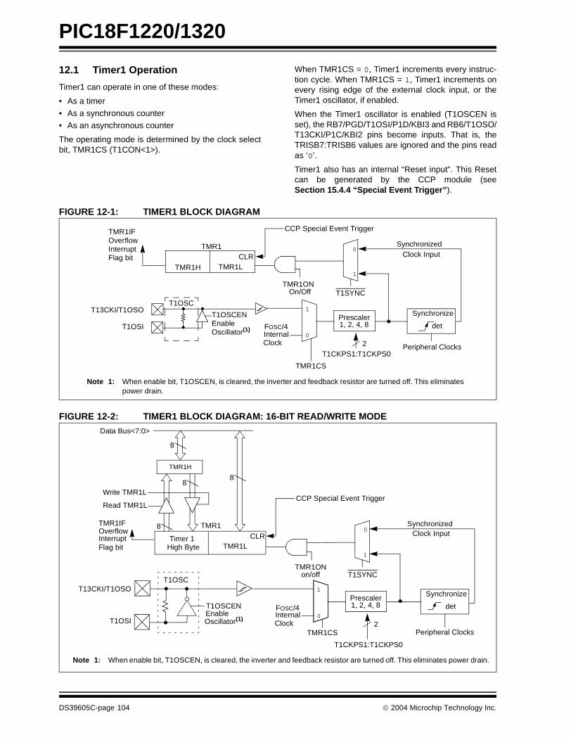
PIC18F1220/1320
12.1 Timer1 Operation
Timer1 can operate in one of these modes:
• As a timer
• As a synchronous counter• As an asynchronous counter
The operating mode is determined by the clock selectbit, TMR1CS (T1CON<1>).
When TMR1CS = 0, Timer1 increments every instruc-tion cycle. When TMR1CS = 1, Timer1 increments onevery rising edge of the external clock input, or theTimer1 oscillator, if enabled.
When the Timer1 oscillator is enabled (T1OSCEN isset), the RB7/PGD/T1OSI/P1D/KBI3 and RB6/T1OSO/T13CKI/P1C/KBI2 pins become inputs. That is, theTRISB7:TRISB6 values are ignored and the pins readas ‘0’.
Timer1 also has an internal “Reset input”. This Resetcan be generated by the CCP module (seeSection 15.4.4 “Special Event Trigger”).
FIGURE 12-1: TIMER1 BLOCK DIAGRAM
FIGURE 12-2: TIMER1 BLOCK DIAGRAM: 16-BIT READ/WRITE MODE
TMR1H TMR1L
T1SYNC
TMR1CS
T1CKPS1:T1CKPS0Peripheral Clocks
FOSC/4InternalClock
TMR1ONOn/Off
Prescaler1, 2, 4, 8
Synchronize
det
1
0
0
1
SynchronizedClock Input
2
TMR1IFOverflow
TMR1CLR
CCP Special Event Trigger
T1OSCENEnableOscillator(1)
T1OSC
InterruptFlag bit
Note 1: When enable bit, T1OSCEN, is cleared, the inverter and feedback resistor are turned off. This eliminatespower drain.
T1OSI
T13CKI/T1OSO
Timer 1 TMR1L
T1OSCT1SYNC
TMR1CS
T1CKPS1:T1CKPS0
Peripheral Clocks
T1OSCENEnableOscillator(1)
TMR1IFOverflowInterrupt
FOSC/4InternalClock
TMR1ONon/off
Prescaler1, 2, 4, 8
Synchronize
det
1
0
0
1
SynchronizedClock Input
2
T13CKI/T1OSO
T1OSI
TMR1
Flag bit
Note 1: When enable bit, T1OSCEN, is cleared, the inverter and feedback resistor are turned off. This eliminates power drain.
High Byte
Data Bus<7:0>
8
TMR1H
88
8
Read TMR1L
Write TMR1L
CLR
CCP Special Event Trigger
DS39605C-page 104 2004 Microchip Technology Inc.
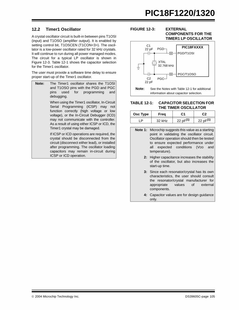
PIC18F1220/1320
12.2 Timer1 Oscillator
A crystal oscillator circuit is built-in between pins T1OSI(input) and T1OSO (amplifier output). It is enabled bysetting control bit, T1OSCEN (T1CON<3>). The oscil-lator is a low-power oscillator rated for 32 kHz crystals.It will continue to run during all power managed modes.The circuit for a typical LP oscillator is shown inFigure 12-3. Table 12-1 shows the capacitor selectionfor the Timer1 oscillator.
The user must provide a software time delay to ensureproper start-up of the Timer1 oscillator.
FIGURE 12-3: EXTERNAL COMPONENTS FOR THE TIMER1 LP OSCILLATOR
TABLE 12-1: CAPACITOR SELECTION FOR THE TIMER OSCILLATOR
Note: The Timer1 oscillator shares the T1OSIand T1OSO pins with the PGD and PGCpins used for programming anddebugging.
When using the Timer1 oscillator, In-CircuitSerial Programming (ICSP) may notfunction correctly (high voltage or lowvoltage), or the In-Circuit Debugger (ICD)may not communicate with the controller.As a result of using either ICSP or ICD, theTimer1 crystal may be damaged.
If ICSP or ICD operations are required, thecrystal should be disconnected from thecircuit (disconnect either lead), or installedafter programming. The oscillator loadingcapacitors may remain in-circuit duringICSP or ICD operation.
Osc Type Freq C1 C2
LP 32 kHz 22 pF(1) 22 pF(1)
Note 1: Microchip suggests this value as a startingpoint in validating the oscillator circuit.Oscillator operation should then be testedto ensure expected performance underall expected conditions (VDD andtemperature).
2: Higher capacitance increases the stabilityof the oscillator, but also increases thestart-up time.
3: Since each resonator/crystal has its owncharacteristics, the user should consultthe resonator/crystal manufacturer forappropriate values of externalcomponents.
4: Capacitor values are for design guidanceonly.
Note: See the Notes with Table 12-1 for additionalinformation about capacitor selection.
C1
C2
XTAL
PIC18FXXXX
PGD/T1OSI
PGC/T1OSO
32.768 kHz
22 pF
22 pF
PGD
PGC
2004 Microchip Technology Inc. DS39605C-page 105

PIC18F1220/1320
12.3 Timer1 Oscillator Layout Considerations
The Timer1 oscillator circuit draws very little powerduring operation. Due to the low-power nature of theoscillator, it may also be sensitive to rapidly changingsignals in close proximity.
The oscillator circuit, shown in Figure 12-3, should belocated as close as possible to the microcontroller.There should be no circuits passing within the oscillatorcircuit boundaries other than VSS or VDD.
If a high-speed circuit must be located near the oscilla-tor (such as the CCP1 pin in output compare or PWMmode, or the primary oscillator using the OSC2 pin), agrounded guard ring around the oscillator circuit, asshown in Figure 12-4, may be helpful when used on asingle sided PCB, or in addition to a ground plane.
FIGURE 12-4: OSCILLATOR CIRCUIT WITH GROUNDED GUARD RING
12.4 Timer1 Interrupt
The TMR1 register pair (TMR1H:TMR1L) incrementsfrom 0000h to FFFFh and rolls over to 0000h. TheTimer1 interrupt, if enabled, is generated on overflow,which is latched in interrupt flag bit, TMR1IF(PIR1<0>). This interrupt can be enabled/disabled bysetting/clearing Timer1 Interrupt Enable bit, TMR1IE(PIE1<0>).
12.5 Resetting Timer1 Using a CCP Trigger Output
If the CCP module is configured in Compare modeto generate a “special event trigger”(CCP1M3:CCP1M0 = 1011), this signal will resetTimer1 and start an A/D conversion, if the A/D mod-ule is enabled (see Section 15.4.4 “Special EventTrigger” for more information).
Timer1 must be configured for either Timer or Synchro-nized Counter mode to take advantage of this feature.If Timer1 is running in Asynchronous Counter mode,this Reset operation may not work.
In the event that a write to Timer1 coincides with aspecial event trigger from CCP1, the write will takeprecedence.
In this mode of operation, the CCPR1H:CCPR1L regis-ter pair effectively becomes the period register forTimer1.
12.6 Timer1 16-Bit Read/Write Mode
Timer1 can be configured for 16-bit reads and writes(see Figure 12-2). When the RD16 control bit(T1CON<7>) is set, the address for TMR1H is mappedto a buffer register for the high byte of Timer1. A readfrom TMR1L will load the contents of the high byte ofTimer1 into the Timer1 high byte buffer. This providesthe user with the ability to accurately read all 16 bits ofTimer1 without having to determine whether a read ofthe high byte, followed by a read of the low byte, isvalid, due to a rollover between reads.
A write to the high byte of Timer1 must also take placethrough the TMR1H Buffer register. Timer1 high byte isupdated with the contents of TMR1H when a writeoccurs to TMR1L. This allows a user to write all 16 bitsto both the high and low bytes of Timer1 at once.
The high byte of Timer1 is not directly readable orwritable in this mode. All reads and writes must takeplace through the Timer1 High Byte Buffer register.Writes to TMR1H do not clear the Timer1 prescaler.The prescaler is only cleared on writes to TMR1L.
RA1
RA4
RB0
MCLR
VSS
RA2
RA3
Note: Not drawn to scale.
RA3
RB2
OSC1
RB5
OSC2
VDD
RB7
RB6
C2X1C3
C4X2C5
C1
Note: The special event triggers from the CCP1module will not set interrupt flag bit,TMR1IF (PIR1<0>).
DS39605C-page 106 2004 Microchip Technology Inc.

PIC18F1220/1320
12.7 Using Timer1 as a Real-Time Clock
Adding an external LP oscillator to Timer1 (such as theone described in Section 12.2 “Timer1 Oscillator”,above), gives users the option to include RTC function-ality to their applications. This is accomplished with aninexpensive watch crystal to provide an accurate timebase and several lines of application code to calculatethe time. When operating in Sleep mode and using abattery or supercapacitor as a power source, it cancompletely eliminate the need for a separate RTCdevice and battery backup.
The application code routine, RTCisr, shown inExample 12-1, demonstrates a simple method toincrement a counter at one-second intervals using anInterrupt Service Routine. Incrementing the TMR1 reg-ister pair to overflow, triggers the interrupt and calls theroutine, which increments the seconds counter by one;additional counters for minutes and hours areincremented as the previous counter overflow.
Since the register pair is 16 bits wide, counting up tooverflow the register directly from a 32.768 kHz clockwould take 2 seconds. To force the overflow at therequired one-second intervals, it is necessary to pre-load it; the simplest method is to set the MSb of TMR1Hwith a BSF instruction. Note that the TMR1L register isnever preloaded or altered; doing so may introducecumulative error over many cycles.
For this method to be accurate, Timer1 must operate inAsynchronous mode and the Timer1 overflow interruptmust be enabled (PIE1<0> = 1), as shown in theroutine, RTCinit. The Timer1 oscillator must also beenabled and running at all times.
EXAMPLE 12-1: IMPLEMENTING A REAL-TIME CLOCK USING A TIMER1 INTERRUPT SERVICERTCinit
MOVLW 0x80 ; Preload TMR1 register pairMOVWF TMR1H ; for 1 second overflowCLRF TMR1LMOVLW b’00001111’ ; Configure for external clock,MOVWF T1OSC ; Asynchronous operation, external oscillatorCLRF secs ; Initialize timekeeping registersCLRF mins ; MOVLW .12MOVWF hoursBSF PIE1, TMR1IE ; Enable Timer1 interruptRETURN
RTCisrBSF TMR1H, 7 ; Preload for 1 sec overflowBCF PIR1, TMR1IF ; Clear interrupt flagINCF secs, F ; Increment secondsMOVLW .59 ; 60 seconds elapsed?CPFSGT secsRETURN ; No, doneCLRF secs ; Clear secondsINCF mins, F ; Increment minutesMOVLW .59 ; 60 minutes elapsed?CPFSGT minsRETURN ; No, doneCLRF mins ; clear minutesINCF hours, F ; Increment hoursMOVLW .23 ; 24 hours elapsed?CPFSGT hoursRETURN ; No, doneMOVLW .01 ; Reset hours to 1MOVWF hoursRETURN ; Done
2004 Microchip Technology Inc. DS39605C-page 107

PIC18F1220/1320
TABLE 12-2: REGISTERS ASSOCIATED WITH TIMER1 AS A TIMER/COUNTER
Name Bit 7 Bit 6 Bit 5 Bit 4 Bit 3 Bit 2 Bit 1 Bit 0Value on
POR, BOR
Value on all other Resets
INTCON GIE/GIEH PEIE/GIEL TMR0IE INT0IE RBIE TMR0IF INT0IF RBIF 0000 000x 0000 000u
PIR1 — ADIF RCIF TXIF — CCP1IF TMR2IF TMR1IF -000 -000 -000 -000
PIE1 — ADIE RCIE TXIE — CCP1IE TMR2IE TMR1IE -000 -000 -000 -000
IPR1 — ADIP RCIP TXIP — CCP1IP TMR2IP TMR1IP -111 -111 -111 -111
TMR1L Holding Register for the Least Significant Byte of the 16-bit TMR1 Register xxxx xxxx uuuu uuuu
TMR1H Holding Register for the Most Significant Byte of the 16-bit TMR1 Register xxxx xxxx uuuu uuuu
T1CON RD16 T1RUN T1CKPS1 T1CKPS0 T1OSCEN T1SYNC TMR1CS TMR1ON 0000 0000 u0uu uuuu
Legend: x = unknown, u = unchanged, – = unimplemented, read as ‘0’. Shaded cells are not used by the Timer1 module.
DS39605C-page 108 2004 Microchip Technology Inc.
PIC18F1220/1320
13.0 TIMER2 MODULE
The Timer2 module timer has the following features:
• 8-bit timer (TMR2 register)• 8-bit period register (PR2)• Readable and writable (both registers)
• Software programmable prescaler (1:1, 1:4, 1:16)• Software programmable postscaler (1:1 to 1:16)• Interrupt on TMR2 match with PR2
Timer2 has a control register shown in Register 13-1.TMR2 can be shut off by clearing control bit, TMR2ON(T2CON<2>), to minimize power consumption.Figure 13-1 is a simplified block diagram of the Timer2module. Register 13-1 shows the Timer2 Controlregister. The prescaler and postscaler selection ofTimer2 are controlled by this register.
13.1 Timer2 Operation
Timer2 can be used as the PWM time base for thePWM mode of the CCP module. The TMR2 register isreadable and writable and is cleared on any deviceReset. The input clock (FOSC/4) has a prescale optionof 1:1, 1:4 or 1:16, selected by control bits,T2CKPS1:T2CKPS0 (T2CON<1:0>). The match out-put of TMR2 goes through a 4-bit postscaler (whichgives a 1:1 to 1:16 scaling inclusive) to generate aTMR2 interrupt (latched in flag bit, TMR2IF (PIR1<1>)).
The prescaler and postscaler counters are clearedwhen any of the following occurs:
• A write to the TMR2 register
• A write to the T2CON register• Any device Reset (Power-on Reset, MCLR Reset,
Watchdog Timer Reset or Brown-out Reset)
TMR2 is not cleared when T2CON is written.
REGISTER 13-1: T2CON: TIMER2 CONTROL REGISTER U-0 R/W-0 R/W-0 R/W-0 R/W-0 R/W-0 R/W-0 R/W-0
— TOUTPS3 TOUTPS2 TOUTPS1 TOUTPS0 TMR2ON T2CKPS1 T2CKPS0
bit 7 bit 0
bit 7 Unimplemented: Read as ‘0’
bit 6-3 TOUTPS3:TOUTPS0: Timer2 Output Postscale Select bits0000 = 1:1 Postscale 0001 = 1:2 Postscale • • • 1111 = 1:16 Postscale
bit 2 TMR2ON: Timer2 On bit1 = Timer2 is on 0 = Timer2 is off
bit 1-0 T2CKPS1:T2CKPS0: Timer2 Clock Prescale Select bits00 = Prescaler is 1 01 = Prescaler is 4 1x = Prescaler is 16
Legend:
R = Readable bit W = Writable bit U = Unimplemented bit, read as ‘0’
-n = Value at POR ‘1’ = Bit is set ‘0’ = Bit is cleared x = Bit is unknown
2004 Microchip Technology Inc. DS39605C-page 109

PIC18F1220/1320
13.2 Timer2 Interrupt
The Timer2 module has an 8-bit period register, PR2.Timer2 increments from 00h until it matches PR2 andthen resets to 00h on the next increment cycle. PR2 isa readable and writable register. The PR2 register isinitialized to FFh upon Reset.
13.3 Output of TMR2
The output of TMR2 (before the postscaler) is fed to theSynchronous Serial Port module, which optionally usesit to generate the shift clock.
FIGURE 13-1: TIMER2 BLOCK DIAGRAM
TABLE 13-1: REGISTERS ASSOCIATED WITH TIMER2 AS A TIMER/COUNTER
Comparator
TMR2Sets Flag
TMR2
Output(1)
Reset
Postscaler
Prescaler
PR2
2
FOSC/4
1:1 to 1:16
1:1, 1:4, 1:16
EQ
4
bit TMR2IF
TOUTPS3:TOUTPS0
T2CKPS1:T2CKPS0
Name Bit 7 Bit 6 Bit 5 Bit 4 Bit 3 Bit 2 Bit 1 Bit 0Value on
POR, BOR
Value on all other Resets
INTCON GIE/GIEH PEIE/GIEL TMR0IE INT0IE RBIE TMR0IF INT0IF RBIF 0000 000x 0000 000u
PIR1 — ADIF RCIF TXIF — CCP1IF TMR2IF TMR1IF -000 -000 -000 -000
PIE1 — ADIE RCIE TXIE — CCP1IE TMR2IE TMR1IE -000 -000 -000 -000
IPR1 — ADIP RCIP TXIP — CCP1IP TMR2IP TMR1IP -111 -111 -111 -111
TMR2 Timer2 Module Register 0000 0000 0000 0000
T2CON — TOUTPS3 TOUTPS2 TOUTPS1 TOUTPS0 TMR2ON T2CKPS1 T2CKPS0 -000 0000 -000 0000
PR2 Timer2 Period Register 1111 1111 1111 1111
Legend: x = unknown, u = unchanged, – = unimplemented, read as ‘0’. Shaded cells are not used by the Timer2 module.
DS39605C-page 110 2004 Microchip Technology Inc.
PIC18F1220/1320
14.0 TIMER3 MODULE
The Timer3 module timer/counter has the followingfeatures:
• 16-bit timer/counter(two 8-bit registers; TMR3H and TMR3L)
• Readable and writable (both registers)
• Internal or external clock select• Interrupt-on-overflow from FFFFh to 0000h• Reset from CCP module trigger
Figure 14-1 is a simplified block diagram of the Timer3module.
Register 14-1 shows the Timer3 Control register. Thisregister controls the operating mode of the Timer3module and sets the CCP clock source.
Register 12-1 shows the Timer1 Control register. Thisregister controls the operating mode of the Timer1module, as well as contains the Timer1 OscillatorEnable bit (T1OSCEN), which can be a clock source forTimer3.
REGISTER 14-1: T3CON: TIMER3 CONTROL REGISTER R/W-0 U-0 R/W-0 R/W-0 R/W-0 R/W-0 R/W-0 R/W-0
RD16 — T3CKPS1 T3CKPS0 T3CCP1 T3SYNC TMR3CS TMR3ON
bit 7 bit 0
bit 7 RD16: 16-bit Read/Write Mode Enable bit
1 = Enables register read/write of Timer3 in one 16-bit operation0 = Enables register read/write of Timer3 in two 8-bit operations
bit 6 Unimplemented: Read as ‘0’
bit 5-4 T3CKPS1:T3CKPS0: Timer3 Input Clock Prescale Select bits11 = 1:8 Prescale value10 = 1:4 Prescale value01 = 1:2 Prescale value00 = 1:1 Prescale value
bit 3 T3CCP1: Timer3 and Timer1 to CCP1 Enable bits1 = Timer3 is the clock source for compare/capture CCP module0 = Timer1 is the clock source for compare/capture CCP module
bit 2 T3SYNC: Timer3 External Clock Input Synchronization Control bit(Not usable if the system clock comes from Timer1/Timer3.)When TMR3CS = 1:1 = Do not synchronize external clock input0 = Synchronize external clock inputWhen TMR3CS = 0:This bit is ignored. Timer3 uses the internal clock when TMR3CS = 0.
bit 1 TMR3CS: Timer3 Clock Source Select bit
1 = External clock input from Timer1 oscillator or T13CKI (on the rising edge after the first falling edge)
0 = Internal clock (FOSC/4)
bit 0 TMR3ON: Timer3 On bit1 = Enables Timer3 0 = Stops Timer3
Legend:
R = Readable bit W = Writable bit U = Unimplemented bit, read as ‘0’
-n = Value at POR ‘1’ = Bit is set ‘0’ = Bit is cleared x = Bit is unknown
2004 Microchip Technology Inc. DS39605C-page 111

PIC18F1220/1320
14.1 Timer3 Operation
Timer3 can operate in one of these modes:
• As a timer
• As a synchronous counter• As an asynchronous counter
The operating mode is determined by the clock selectbit, TMR3CS (T3CON<1>).
When TMR3CS = 0, Timer3 increments every instruc-tion cycle. When TMR3CS = 1, Timer3 increments onevery rising edge of the Timer1 external clock input orthe Timer1 oscillator, if enabled.
When the Timer1 oscillator is enabled (T1OSCEN isset), the RB7/PGD/T1OSI/P1D/KBI3 and RB6/PGC/T1OSO/T13CKI/P1C/KBI2 pins become inputs. Thatis, the TRISB7:TRISB6 value is ignored and the pinsare read as ‘0’.
Timer3 also has an internal “Reset input”. This Resetcan be generated by the CCP module (seeSection 15.4.4 “Special Event Trigger”).
FIGURE 14-1: TIMER3 BLOCK DIAGRAM
FIGURE 14-2: TIMER3 BLOCK DIAGRAM CONFIGURED IN 16-BIT READ/WRITE MODE
TMR3H TMR3L
T1OSC
T3SYNC
TMR3CS
T3CKPS1:T3CKPS0
Peripheral Clocks
T1OSCENEnableOscillator(1)
TMR3IFOverflowInterrupt
FOSC/4InternalClock
TMR3ONOn/Off
Prescaler1, 2, 4, 8
Synchronize
det
1
0
0
1
SynchronizedClock Input
2
T1OSO/
T1OSI
Flag bit
Note 1: When enable bit, T1OSCEN, is cleared, the inverter and feedback resistor are turned off. This eliminates power drain.
T13CKI
CLR
CCP Special Event TriggerT3CCPx
Timer3TMR3L
T1OSCT3SYNC
TMR3CS
T3CKPS1:T3CKPS0Peripheral
T1OSCENEnableOscillator(1)
FOSC/4InternalClock
TMR3ONOn/Off
Prescaler1, 2, 4, 8
Synchronize
det
1
0
0
1
SynchronizedClock Input
2
T1OSO/
T1OSI
TMR3
T13CKI
CLR
CCP Special Event TriggerT3CCPx
To Timer1 Clock Input
Note 1: When the T1OSCEN bit is cleared, the inverter and feedback resistor are turned off. This eliminates power drain.
High Byte
Data Bus<7:0>
8
TMR3H
88
8
Read TMR3L
Write TMR3L
Set TMR3IF Flag biton Overflow
Clocks
DS39605C-page 112 2004 Microchip Technology Inc.
PIC18F1220/1320
14.2 Timer1 Oscillator
The Timer1 oscillator may be used as the clock sourcefor Timer3. The Timer1 oscillator is enabled by settingthe T1OSCEN (T1CON<3>) bit. The oscillator is a low-power oscillator rated for 32 kHz crystals. SeeSection 12.2 “Timer1 Oscillator” for further details.
14.3 Timer3 Interrupt
The TMR3 register pair (TMR3H:TMR3L) incrementsfrom 0000h to FFFFh and rolls over to 0000h. TheTMR3 interrupt, if enabled, is generated on overflow,which is latched in interrupt flag bit, TMR3IF(PIR2<1>). This interrupt can be enabled/disabled bysetting/clearing TMR3 Interrupt Enable bit, TMR3IE(PIE2<1>).
14.4 Resetting Timer3 Using a CCP Trigger Output
If the CCP module is configured in Compare modeto generate a “special event trigger”(CCP1M3:CCP1M0 = 1011), this signal will resetTimer3. See Section 15.4.4 “Special Event Trigger”for more information.
Timer3 must be configured for either Timer or Synchro-nized Counter mode to take advantage of this feature.If Timer3 is running in Asynchronous Counter mode,this Reset operation may not work. In the event that awrite to Timer3 coincides with a special event triggerfrom CCP1, the write will take precedence. In this modeof operation, the CCPR1H:CCPR1L register paireffectively becomes the period register for Timer3.
TABLE 14-1: REGISTERS ASSOCIATED WITH TIMER3 AS A TIMER/COUNTER
Note: The special event triggers from the CCPmodule will not set interrupt flag bit,TMR3IF (PIR1<0>).
Name Bit 7 Bit 6 Bit 5 Bit 4 Bit 3 Bit 2 Bit 1 Bit 0Value on
POR, BOR
Value onall other Resets
INTCON GIE/GIEH
PEIE/GIEL
TMR0IE INT0IE RBIE TMR0IF INT0IF RBIF 0000 000x 0000 000u
PIR2 OSCFIF — — EEIF — LVDIF TMR3IF — 0--0 -00- 0--0 -00-
PIE2 OSCFIE — — EEIE — LVDIE TMR3IE — 0--0 -00- 0--0 -00-
IPR2 OSCFIP — — EEIP — LVDIP TMR3IP — 1--1 -11- 1--1 -11-
TMR3L Holding Register for the Least Significant Byte of the 16-bit TMR3 Register xxxx xxxx uuuu uuuu
TMR3H Holding Register for the Most Significant Byte of the 16-bit TMR3 Register xxxx xxxx uuuu uuuu
T1CON RD16 T1RUN T1CKPS1 T1CKPS0 T1OSCEN T1SYNC TMR1CS TMR1ON 0000 0000 u0uu uuuu
T3CON RD16 — T3CKPS1 T3CKPS0 T3CCP1 T3SYNC TMR3CS TMR3ON 0-00 0000 u-uu uuuu
Legend: x = unknown, u = unchanged, – = unimplemented, read as ‘0’. Shaded cells are not used by the Timer3 module.
2004 Microchip Technology Inc. DS39605C-page 113

PIC18F1220/1320
NOTES:
DS39605C-page 114 2004 Microchip Technology Inc.
PIC18F1220/1320
15.0 ENHANCED CAPTURE/COMPARE/PWM (ECCP) MODULE
The Enhanced CCP module is implemented as astandard CCP module with Enhanced PWMcapabilities. These capabilities allow for 2 or 4 outputchannels, user-selectable polarity, dead-band controland automatic shutdown and restart and are discussedin detail in Section 15.5 “Enhanced PWM Mode”.
The control register for CCP1 is shown in Register 15-1.
In addition to the expanded functions of the CCP1CONregister, the ECCP module has two additionalregisters associated with Enhanced PWM operationand auto-shutdown features:
• PWM1CON• ECCPAS
REGISTER 15-1: CCP1CON REGISTER FOR ENHANCED CCP OPERATION R/W-0 R/W-0 R/W-0 R/W-0 R/W-0 R/W-0 R/W-0 R/W-0
P1M1 P1M0 DC1B1 DC1B0 CCP1M3 CCP1M2 CCP1M1 CCP1M0
bit 7 bit 0
bit 7-6 P1M1:P1M0: PWM Output Configuration bitsIf CCP1M<3:2> = 00, 01, 10:xx = P1A assigned as Capture/Compare input; P1B, P1C, P1D assigned as port pinsIf CCP1M<3:2> = 11:00 = Single output; P1A modulated; P1B, P1C, P1D assigned as port pins01 = Full-bridge output forward; P1D modulated; P1A active; P1B, P1C inactive10 = Half-bridge output; P1A, P1B modulated with dead-band control; P1C, P1D assigned as
port pins11 = Full-bridge output reverse; P1B modulated; P1C active; P1A, P1D inactive
bit 5-4 DC1B1:DC1B0: PWM Duty Cycle Least Significant bits
Capture mode:Unused.
Compare mode:Unused.
PWM mode:These bits are the two LSbs of the PWM duty cycle. The eight MSbs are found in CCPR1L.
bit 3-0 CCP1M3:CCP1M0: ECCP1 Mode Select bits0000 = Capture/Compare/PWM off (resets ECCP module)0001 = Unused (reserved)0010 = Compare mode, toggle output on match (ECCP1IF bit is set)0011 = Unused (reserved)0100 = Capture mode, every falling edge0101 = Capture mode, every rising edge0110 = Capture mode, every 4th rising edge0111 = Capture mode, every 16th rising edge1000 = Compare mode, set output on match (ECCP1IF bit is set)1001 = Compare mode, clear output on match (ECCP1IF bit is set)1010 = Compare mode, generate software interrupt on match (ECCP1IF bit is set,
ECCP1 pin returns to port pin operation)1011 = Compare mode, trigger special event (ECCP1IF bit is set; ECCP resets TMR1 or
TMR3 and starts an A/D conversion if the A/D module is enabled)1100 = PWM mode; P1A, P1C active-high; P1B, P1D active-high1101 = PWM mode; P1A, P1C active-high; P1B, P1D active-low1110 = PWM mode; P1A, P1C active-low; P1B, P1D active-high1111 = PWM mode; P1A, P1C active-low; P1B, P1D active-low
Legend:R = Readable bit W = Writable bit U = Unimplemented bit, read as ‘0’
-n = Value at POR ‘1’ = Bit is set ‘0’ = Bit is cleared x = Bit is unknown
2004 Microchip Technology Inc. DS39605C-page 115
PIC18F1220/1320
15.1 ECCP Outputs
The Enhanced CCP module may have up to fouroutputs, depending on the selected operating mode.These outputs, designated P1A through P1D, aremultiplexed with I/O pins on PORTB. The pinassignments are summarized in Table 15-1.
To configure I/O pins as PWM outputs, the proper PWMmode must be selected by setting the P1Mn andCCP1Mn bits (CCP1CON<7:6> and <3:0>,respectively). The appropriate TRISB direction bits forthe port pins must also be set as outputs.
TABLE 15-1: PIN ASSIGNMENTS FOR VARIOUS ECCP MODES
15.2 CCP Module
Capture/Compare/PWM Register 1 (CCPR1) is com-prised of two 8-bit registers: CCPR1L (low byte) andCCPR1H (high byte). The CCP1CON register controlsthe operation of CCP1. All are readable and writable.
TABLE 15-2: CCP MODE – TIMER RESOURCE
15.3 Capture Mode
In Capture mode, CCPR1H:CCPR1L captures the 16-bitvalue of the TMR1 or TMR3 registers when an eventoccurs on pin RB3/CCP1/P1A. An event is defined asone of the following:
• every falling edge
• every rising edge• every 4th rising edge• every 16th rising edge
The event is selected by control bits, CCP1M3:CCP1M0(CCP1CON<3:0>). When a capture is made, the inter-rupt request flag bit, CCP1IF (PIR1<2>), is set; it mustbe cleared in software. If another capture occurs beforethe value in register CCPR1 is read, the old capturedvalue is overwritten by the new captured value.
15.3.1 CCP PIN CONFIGURATION
In Capture mode, the RB3/CCP1/P1A pin should beconfigured as an input by setting the TRISB<3> bit.
15.3.2 TIMER1/TIMER3 MODE SELECTION
The timers that are to be used with the capture feature(either Timer1 and/or Timer3) must be running in Timermode or Synchronized Counter mode. In Asynchro-nous Counter mode, the capture operation may notwork. The timer to be used with the CCP module isselected in the T3CON register.
15.3.3 SOFTWARE INTERRUPT
When the Capture mode is changed, a false captureinterrupt may be generated. The user should keep bit,CCP1IE (PIE1<2>), clear while changing capturemodes to avoid false interrupts and should clear theflag bit, CCP1IF, following any such change inoperating mode.
ECCP ModeCCP1CON
ConfigurationRB3 RB2 RB6 RB7
Compatible CCP 00xx 11xx CCP1 RB2/INT2 RB6/PGC/T1OSO/T13CKI/KBI2 RB7/PGD/T1OSI/KBI3
Dual PWM 10xx 11xx P1A P1B RB6/PGC/T1OSO/T13CKI/KBI2 RB7/PGD/T1OSI/KBI3
Quad PWM x1xx 11xx P1A P1B P1C P1D
Legend: x = Don’t care. Shaded cells indicate pin assignments not used by ECCP in a given mode.Note 1: TRIS register values must be configured appropriately.
CCP Mode Timer Resource
CaptureCompare
PWM
Timer1 or Timer3Timer1 or Timer3
Timer2
Note: If the RB3/CCP1/P1A is configured as anoutput, a write to the port can cause acapture condition.
DS39605C-page 116 2004 Microchip Technology Inc.

PIC18F1220/1320
15.3.4 CCP PRESCALER
There are four prescaler settings, specified by bitsCCP1M3:CCP1M0. Whenever the CCP module isturned off or the CCP module is not in Capture mode,the prescaler counter is cleared. This means that anyReset will clear the prescaler counter.
Switching from one capture prescaler to another maygenerate an interrupt. Also, the prescaler counter willnot be cleared; therefore, the first capture may be froma non-zero prescaler. Example 15-1 shows the
recommended method for switching between captureprescalers. This example also clears the prescalercounter and will not generate the “false” interrupt.
EXAMPLE 15-1: CHANGING BETWEEN CAPTURE PRESCALERS
FIGURE 15-1: CAPTURE MODE OPERATION BLOCK DIAGRAM
15.4 Compare Mode
In Compare mode, the 16-bit CCPR1 register value isconstantly compared against either the TMR1 registerpair value, or the TMR3 register pair value. When amatch occurs, the RB3/CCP1/P1A pin:
• Is driven high• Is driven low
• Toggles output (high-to-low or low-to-high) • Remains unchanged (interrupt only)
The action on the pin is based on the value of controlbits, CCP1M3:CCP1M0. At the same time, interruptflag bit, CCP1IF, is set.
15.4.1 CCP PIN CONFIGURATION
The user must configure the RB3/CCP1/P1A pin as anoutput by clearing the TRISB<3> bit.
15.4.2 TIMER1/TIMER3 MODE SELECTION
Timer1 and/or Timer3 must be running in Timer modeor Synchronized Counter mode if the CCP module isusing the compare feature. In Asynchronous Countermode, the compare operation may not work.
15.4.3 SOFTWARE INTERRUPT MODE
When generate software interrupt is chosen, the RB3/CCP1/P1A pin is not affected. CCP1IF is set and aninterrupt is generated (if enabled).
15.4.4 SPECIAL EVENT TRIGGER
In this mode, an internal hardware trigger is generated,which may be used to initiate an action.
The special event trigger output of CCP1 resets theTMR1 register pair. This allows the CCPR1 register toeffectively be a 16-bit programmable period register forTimer1.
The special event trigger also sets the GO/DONE bit(ADCON0<1>). This starts a conversion of thecurrently selected A/D channel if the A/D is on.
CLRF CCP1CON ; Turn CCP module offMOVLW NEW_CAPT_PS ; Load WREG with the
; new prescaler mode; value and CCP ON
MOVWF CCP1CON ; Load CCP1CON with; this value
CCPR1H CCPR1L
TMR1H TMR1L
Set Flag bit CCP1IF
TMR3Enable
Q’sCCP1CON<3:0>
CCP1 pin
Prescaler÷ 1, 4, 16
andEdge Detect
TMR3H TMR3L
TMR1Enable
T3CCP1
T3CCP1
Note: Clearing the CCP1CON register will forcethe RB3/CCP1/P1A compare output latchto the default low level. This is not thePORTB I/O data latch.
2004 Microchip Technology Inc. DS39605C-page 117
PIC18F1220/1320
FIGURE 15-2: COMPARE MODE OPERATION BLOCK DIAGRAM
TABLE 15-3: REGISTERS ASSOCIATED WITH CAPTURE, COMPARE, TIMER1 AND TIMER3
CCPR1H CCPR1L
TMR1H TMR1L
ComparatorQ S
R
OutputLogic
Special Event Trigger
Set Flag bit CCP1IF
MatchRB3/CCP1/P1A pin
TRISB<3>CCP1CON<3:0>
Mode SelectOutput Enable
Special Event Trigger will:Reset Timer1 or Timer3, but does not set Timer1 or Timer3 interrupt flag bitand set bit GO/DONE (ADCON0<2>), which starts an A/D conversion.
TMR3H TMR3L
T3CCP1 10
Name Bit 7 Bit 6 Bit 5 Bit 4 Bit 3 Bit 2 Bit 1 Bit 0Value on
POR, BOR
Value onall otherResets
INTCON GIE/GIEH PEIE/GIEL TMR0IE INT0IE RBIE TMR0IF INT0IF RBIF 0000 000x 0000 000u
PIR1 — ADIF RCIF TXIF — CCP1IF TMR2IF TMR1IF -000 -000 -000 -000
PIE1 — ADIE RCIE TXIE — CCP1IE TMR2IE TMR1IE -000 -000 -000 -000
IPR1 — ADIP RCIP TXIP — CCP1IP TMR2IP TMR1IP -111 -111 -111 -111
TRISB PORTB Data Direction Register 1111 1111 1111 1111
TMR1L Holding Register for the Least Significant Byte of the 16-bit TMR1 Register xxxx xxxx uuuu uuuu
TMR1H Holding Register for the Most Significant Byte of the 16-bit TMR1 Register xxxx xxxx uuuu uuuu
T1CON RD16 T1RUN T1CKPS1 T1CKPS0 T1OSCEN T1SYNC TMR1CS TMR1ON 0000 0000 uuuu uuuu
CCPR1L Capture/Compare/PWM Register 1 (LSB) xxxx xxxx uuuu uuuu
CCPR1H Capture/Compare/PWM Register 1 (MSB) xxxx xxxx uuuu uuuu
CCP1CON P1M1 P1M0 DC1B1 DC1B0 CCP1M3 CCP1M2 CCP1M1 CCP1M0 0000 0000 0000 0000
TMR3L Holding Register for the Least Significant Byte of the 16-bit TMR3 Register xxxx xxxx uuuu uuuu
TMR3H Holding Register for the Most Significant Byte of the 16-bit TMR3 Register xxxx xxxx uuuu uuuu
T3CON RD16 — T3CKPS1 T3CKPS0 T3CCP1 T3SYNC TMR3CS TMR3ON 0-00 0000 u-uu uuuu
ADCON0 VCFG1 VCFG0 — CHS2 CHS1 CHS0 GO/DONE ADON 00-0 0000 00-0 0000
Legend: x = unknown, u = unchanged, – = unimplemented, read as ‘0’. Shaded cells are not used by Capture and Timer1.
DS39605C-page 118 2004 Microchip Technology Inc.
PIC18F1220/1320
15.5 Enhanced PWM Mode
The Enhanced PWM Mode provides additional PWMoutput options for a broader range of control applica-tions. The module is an upwardly compatible version ofthe standard CCP module and offers up to four outputs,designated P1A through P1D. Users are also able toselect the polarity of the signal (either active-high oractive-low). The module’s output mode and polarity areconfigured by setting the P1M1:P1M0 andCCP1M3CCP1M0 bits of the CCP1CON register(CCP1CON<7:6> and CCP1CON<3:0>, respectively).
Figure 15-3 shows a simplified block diagram of PWMoperation. All control registers are double-buffered andare loaded at the beginning of a new PWM cycle (theperiod boundary when Timer2 resets) in order to preventglitches on any of the outputs. The exception is the PWMDelay register, ECCP1DEL, which is loaded at either theduty cycle boundary or the boundary period (whichevercomes first). Because of the buffering, the module waitsuntil the assigned timer resets instead of starting imme-diately. This means that Enhanced PWM waveforms donot exactly match the standard PWM waveforms, butare instead offset by one full instruction cycle (4 TOSC).
As before, the user must manually configure theappropriate TRIS bits for output.
15.5.1 PWM PERIOD
The PWM period is specified by writing to the PR2register. The PWM period can be calculated using theequation:
EQUATION 15-1: PWM PERIOD
PWM frequency is defined as 1/[PWM period]. WhenTMR2 is equal to PR2, the following three events occuron the next increment cycle:
• TMR2 is cleared
• The CCP1 pin is set (if PWM duty cycle = 0%, the CCP1 pin will not be set)
• The PWM duty cycle is copied from CCPR1L into CCPR1H
15.5.2 PWM DUTY CYCLE
The PWM duty cycle is specified by writing to theCCPR1L register and to the CCP1CON<5:4> bits. Upto 10-bit resolution is available. The CCPR1L containsthe eight MSbs and the CCP1CON<5:4> contains thetwo LSbs. This 10-bit value is represented byCCPR1L:CCP1CON<5:4>. The PWM duty cycle iscalculated by the equation:
EQUATION 15-2: PWM DUTY CYCLE
CCPR1L and CCP1CON<5:4> can be written to at anytime, but the duty cycle value is not copied intoCCPR1H until a match between PR2 and TMR2 occurs(i.e., the period is complete). In PWM mode, CCPR1His a read-only register.
The CCPR1H register and a 2-bit internal latch areused to double-buffer the PWM duty cycle. Thisdouble-buffering is essential for glitchless PWMoperation. When the CCPR1H and 2-bit latch matchTMR2, concatenated with an internal 2-bit Q clock ortwo bits of the TMR2 prescaler, the CCP1 pin iscleared. The maximum PWM resolution (bits) for agiven PWM frequency is given by the equation:
EQUATION 15-3: PWM RESOLUTION
15.5.3 PWM OUTPUT CONFIGURATIONS
The P1M1:P1M0 bits in the CCP1CON register allowone of four configurations:
• Single Output
• Half-Bridge Output • Full-Bridge Output, Forward mode• Full-Bridge Output, Reverse mode
The Single Output mode is the Standard PWM modediscussed in Section 15.5 “Enhanced PWM Mode”.The Half-Bridge and Full-Bridge Output modes arecovered in detail in the sections that follow.
The general relationship of the outputs in allconfigurations is summarized in Figure 15-4.
TABLE 15-4: EXAMPLE PWM FREQUENCIES AND RESOLUTIONS AT 40 MHz
Note: The Timer2 postscaler (see Section 13.0“Timer2 Module”) is not used in thedetermination of the PWM frequency. Thepostscaler could be used to have a servoupdate rate at a different frequency thanthe PWM output.
PWM Period = [(PR2) + 1] • 4 • TOSC •(TMR2 Prescale Value)
Note: If the PWM duty cycle value is longer thanthe PWM period, the CCP1 pin will not becleared.
PWM Duty Cycle = (CCPR1L:CCP1CON<5:4>) •TOSC • (TMR2 Prescale Value)
( )PWM Resolution (max) =
FOSC
FPWMlog
log(2)bits
PWM Frequency 2.44 kHz 9.77 kHz 39.06 kHz 156.25 kHz 312.50 kHz 416.67 kHz
Timer Prescaler (1, 4, 16) 16 4 1 1 1 1
PR2 Value FFh FFh FFh 3Fh 1Fh 17h
Maximum Resolution (bits) 10 10 10 8 7 6.58
2004 Microchip Technology Inc. DS39605C-page 119
PIC18F1220/1320
FIGURE 15-3: SIMPLIFIED BLOCK DIAGRAM OF THE ENHANCED PWM MODULE
FIGURE 15-4: PWM OUTPUT RELATIONSHIPS (ACTIVE-HIGH STATE)
CCPR1L
CCPR1H (Slave)
Comparator
TMR2
Comparator
PR2
(Note 1)
R Q
S
Duty Cycle RegistersCCP1CON<5:4>
Clear Timer,set CCP1 pin and latch D.C.
Note: The 8-bit TMR2 register is concatenated with the 2-bit internal Q clock, or 2 bits of the prescaler to create the 10-bit time base.
TRISB<3>
RB3/CCP1/P1A
TRISB<2>
RB2/P1B/INT2
TRISB<6>
RB6/PGC/T1OSO/T13CKI/
TRISB<7>
RB7/PGD/T1OSI/P1D/KBI3
OutputController
P1M1<1:0>2
CCP1M<3:0>4
CCP1DEL
CCP1/P1A
P1B
P1C
P1D
P1C/KBI2
0
Period
00
10
01
11
SIGNALPR2+1
CCP1CON<7:6>
P1A Modulated
P1A Modulated
P1B Modulated
P1A Active
P1B Inactive
P1C Inactive
P1D Modulated
P1A Inactive
P1B Modulated
P1C Active
P1D Inactive
DutyCycle
(Single Output)
(Half-Bridge)
(Full-Bridge,Forward)
(Full-Bridge,Reverse)
Delay(1) Delay(1)
DS39605C-page 120 2004 Microchip Technology Inc.
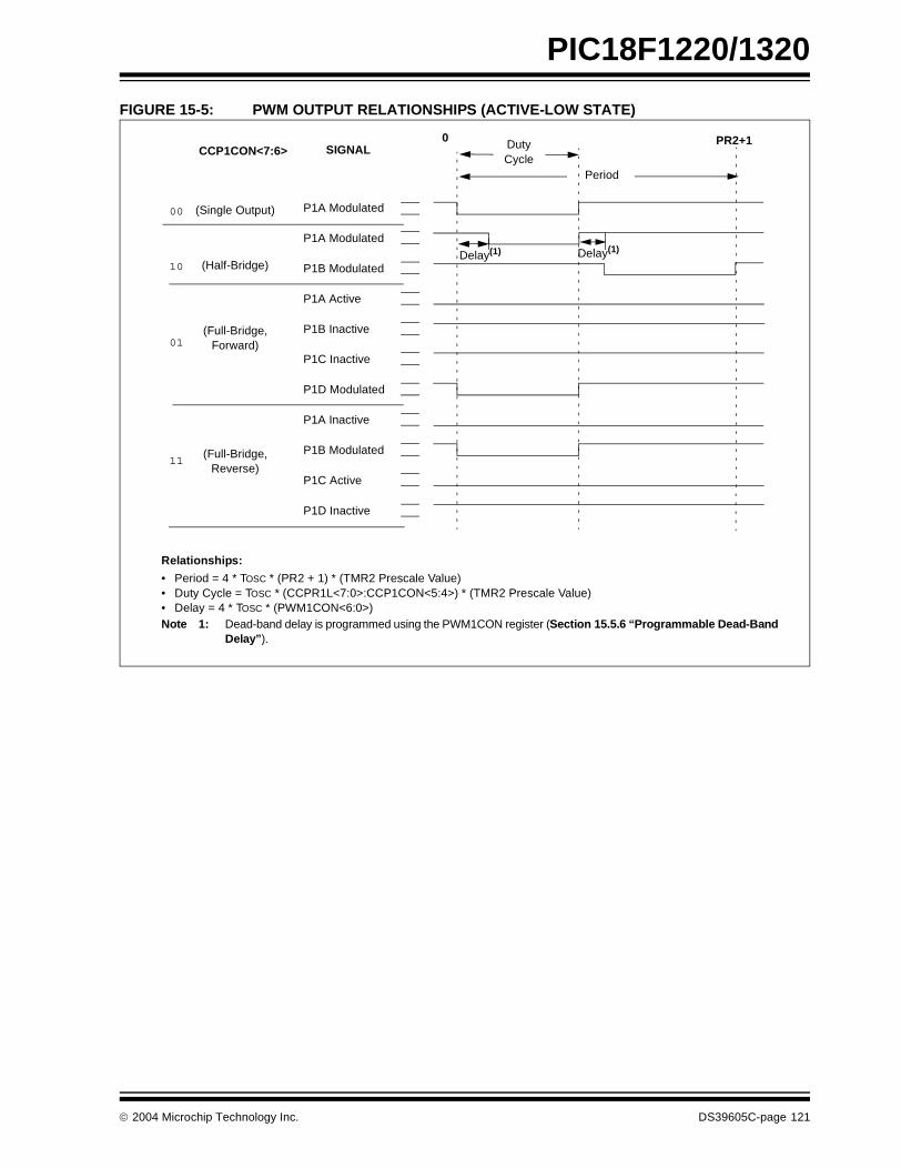
PIC18F1220/1320
FIGURE 15-5: PWM OUTPUT RELATIONSHIPS (ACTIVE-LOW STATE)
0
Period
00
10
01
11
SIGNALPR2+1
CCP1CON<7:6>
P1A Modulated
P1A Modulated
P1B Modulated
P1A Active
P1B Inactive
P1C Inactive
P1D Modulated
P1A Inactive
P1B Modulated
P1C Active
P1D Inactive
DutyCycle
(Single Output)
(Half-Bridge)
(Full-Bridge,Forward)
(Full-Bridge,Reverse)
Delay(1) Delay(1)
Relationships:
• Period = 4 * TOSC * (PR2 + 1) * (TMR2 Prescale Value)• Duty Cycle = TOSC * (CCPR1L<7:0>:CCP1CON<5:4>) * (TMR2 Prescale Value)• Delay = 4 * TOSC * (PWM1CON<6:0>)Note 1: Dead-band delay is programmed using the PWM1CON register (Section 15.5.6 “Programmable Dead-Band
Delay”).
2004 Microchip Technology Inc. DS39605C-page 121

PIC18F1220/1320
15.5.4 HALF-BRIDGE MODE
In the Half-Bridge Output mode, two pins are used asoutputs to drive push-pull loads. The PWM outputsignal is output on the RB3/CCP1/P1A pin, while thecomplementary PWM output signal is output on theRB2/P1B/INT2 pin (Figure 15-6). This mode can beused for half-bridge applications, as shown inFigure 15-7, or for full-bridge applications, where fourpower switches are being modulated with two PWMsignals.
In Half-Bridge Output mode, the programmable dead-band delay can be used to prevent shoot-throughcurrent in half-bridge power devices. The value of bits,PDC6:PDC0 (PWM1CON<6:0>), sets the number ofinstruction cycles before the output is driven active. If thevalue is greater than the duty cycle, the correspondingoutput remains inactive during the entire cycle. SeeSection 15.5.6 “Programmable Dead-Band Delay”for more details of the dead-band delay operations.
The TRISB<3> and TRISB<2> bits must be cleared toconfigure P1A and P1B as outputs.
FIGURE 15-6: HALF-BRIDGE PWM OUTPUT (ACTIVE-HIGH)
FIGURE 15-7: EXAMPLES OF HALF-BRIDGE OUTPUT MODE APPLICATIONS
Period
Duty Cycle
td
td
(1)
P1A
P1B
td = Dead-Band Delay
Period
(1) (1)
Note 1: At this time, the TMR2 register is equal to thePR2 register.
PIC18F1220/1320
P1A
P1B
FETDriver
FETDriver
Load
+V-
+V-
FETDriver
FETDriver
V+
V-
Load
FETDriver
FETDriver
PIC18F1220/1320
P1A
P1B
Standard Half-Bridge Circuit (“Push-Pull”)
Half-Bridge Output Driving a Full-Bridge Circuit
DS39605C-page 122 2004 Microchip Technology Inc.
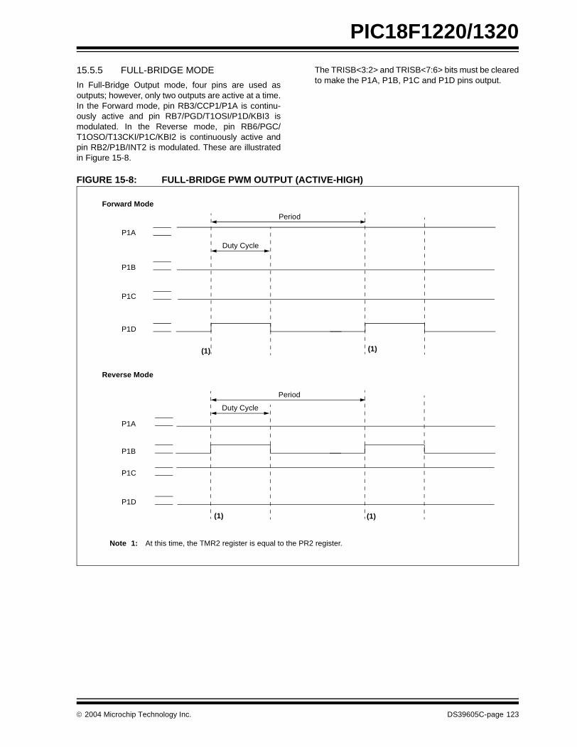
PIC18F1220/1320
15.5.5 FULL-BRIDGE MODE
In Full-Bridge Output mode, four pins are used asoutputs; however, only two outputs are active at a time.In the Forward mode, pin RB3/CCP1/P1A is continu-ously active and pin RB7/PGD/T1OSI/P1D/KBI3 ismodulated. In the Reverse mode, pin RB6/PGC/T1OSO/T13CKI/P1C/KBI2 is continuously active andpin RB2/P1B/INT2 is modulated. These are illustratedin Figure 15-8.
The TRISB<3:2> and TRISB<7:6> bits must be clearedto make the P1A, P1B, P1C and P1D pins output.
FIGURE 15-8: FULL-BRIDGE PWM OUTPUT (ACTIVE-HIGH)
Period
Duty Cycle
P1A
P1B
P1C
P1D
Forward Mode
(1)
Period
Duty Cycle
P1A
P1C
P1D
P1B
Reverse Mode
(1)
(1)(1)
Note 1: At this time, the TMR2 register is equal to the PR2 register.
2004 Microchip Technology Inc. DS39605C-page 123

PIC18F1220/1320
FIGURE 15-9: EXAMPLE OF FULL-BRIDGE APPLICATION
15.5.5.1 Direction Change in Full-Bridge Mode
In the Full-Bridge Output mode, the P1M1 bit in theCCP1CON register allows the user to control theForward/Reverse direction. When the applicationfirmware changes this direction control bit, the modulewill assume the new direction on the next PWM cycle.
Just before the end of the current PWM period, themodulated outputs (P1B and P1D) are placed in theirinactive state, while the unmodulated outputs (P1A andP1C) are switched to drive in the opposite direction.This occurs in a time interval of (4 TOSC * (Timer2Prescale Value) before the next PWM period begins.The Timer2 prescaler will be either 1,4 or 16, depend-ing on the value of the T2CKPS bit (T2CON<1:0>).During the interval from the switch of the unmodulatedoutputs to the beginning of the next period, themodulated outputs (P1B and P1D) remain inactive.This relationship is shown in Figure 15-10.
Note that in the Full-Bridge Output mode, the ECCPmodule does not provide any dead-band delay. Ingeneral, since only one output is modulated at all times,dead-band delay is not required. However, there is asituation where a dead-band delay might be required.This situation occurs when both of the followingconditions are true:
1. The direction of the PWM output changes whenthe duty cycle of the output is at or near 100%.
2. The turn-off time of the power switch, includingthe power device and driver circuit, is greaterthan the turn-on time.
Figure 15-11 shows an example where the PWM direc-tion changes from forward to reverse, at a near 100%duty cycle. At time t1, the output P1A and P1D becomeinactive, while output P1C becomes active. In thisexample, since the turn-off time of the power devices islonger than the turn-on time, a shoot-through currentmay flow through power devices QC and QD (seeFigure 15-9) for the duration of ‘t’. The same phenom-enon will occur to power devices QA and QB for PWMdirection change from reverse to forward.
If changing PWM direction at high duty cycle is requiredfor an application, one of the following requirementsmust be met:
1. Reduce PWM for a PWM period beforechanging directions.
2. Use switch drivers that can drive the switches offfaster than they can drive them on.
Other options to prevent shoot-through current mayexist.
PIC18F1220/1320
P1A
P1C
FETDriver
FETDriver
V+
V-
Load
FETDriver
FETDriver
P1B
P1D
QA
QB QD
QC
DS39605C-page 124 2004 Microchip Technology Inc.
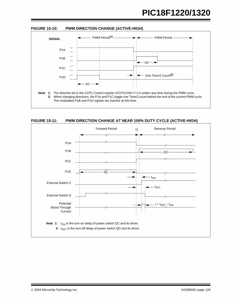
PIC18F1220/1320
FIGURE 15-10: PWM DIRECTION CHANGE (ACTIVE-HIGH)
FIGURE 15-11: PWM DIRECTION CHANGE AT NEAR 100% DUTY CYCLE (ACTIVE-HIGH)
DC
PWM Period(1)SIGNAL
Note 1: The direction bit in the CCP1 Control register (CCP1CON<7>) is written any time during the PWM cycle.2: When changing directions, the P1A and P1C toggle one Timer2 count before the end of the current PWM cycle.
The modulated P1B and P1D signals are inactive at this time.
PWM Period
One Timer2 Count(2)
P1A
P1B
P1C
P1D
DC
Forward Period Reverse Period
P1A
tON
tOFF
t = tOFF – tON
P1B
P1C
P1D
External Switch D
PotentialShoot-Through
Current
Note 1: tON is the turn-on delay of power switch QC and its driver.
2: tOFF is the turn-off delay of power switch QD and its driver.
External Switch C
t1
DC
DC
2004 Microchip Technology Inc. DS39605C-page 125

PIC18F1220/1320
15.5.6 PROGRAMMABLE DEAD-BAND DELAY
In half-bridge applications where all power switches aremodulated at the PWM frequency at all times, thepower switches normally require more time to turn offthan to turn on. If both the upper and lower powerswitches are switched at the same time (one turned onand the other turned off), both switches may be on fora short period of time until one switch completely turnsoff. During this brief interval, a very high current (shoot-through current) may flow through both powerswitches, shorting the bridge supply. To avoid thispotentially destructive shoot-through current from flow-ing during switching, turning on either of the powerswitches is normally delayed to allow the other switchto completely turn off.
In the Half-Bridge Output mode, a digitally programmabledead-band delay is available to avoid shoot-throughcurrent from destroying the bridge power switches. Thedelay occurs at the signal transition from the non-activestate to the active state. See Figure 15-6 for an illustra-tion. The lower seven bits of the PWM1CON register(Register 15-2) sets the delay period in terms ofmicrocontroller instruction cycles (TCY or 4 TOSC).
15.5.7 ENHANCED PWM AUTO-SHUTDOWN
When the ECCP is programmed for any of theEnhanced PWM modes, the active output pins may beconfigured for auto-shutdown. Auto-shutdown immedi-ately places the Enhanced PWM output pins into adefined shutdown state when a shutdown eventoccurs.
A shutdown event can be caused by the INT0, INT1 orINT2 pins (or any combination of these three sources).The auto-shutdown feature can be disabled by notselecting any auto-shutdown sources. The auto-shutdown sources to be used are selected using theECCPAS2:ECCPAS0 bits (bits <6:4> of the ECCPASregister).
When a shutdown occurs, the output pins areasynchronously placed in their shutdown states, spec-ified by the PSSAC1:PSSAC0 and PSSBD1:PSSBD0bits (ECCPAS<3:0>). Each pin pair (P1A/P1C andP1B/P1D) may be set to drive high, drive low or be tri-stated (not driving). The ECCPASE bit (ECCPAS<7>)is also set to hold the Enhanced PWM outputs in theirshutdown states.
The ECCPASE bit is set by hardware when a shutdownevent occurs. If automatic restarts are not enabled, theECCPASE bit is cleared by firmware when the cause ofthe shutdown clears. If automatic restarts are enabled,the ECCPASE bit is automatically cleared when thecause of the auto-shutdown has cleared.
If the ECCPASE bit is set when a PWM period begins,the PWM outputs remain in their shutdown state for thatentire PWM period. When the ECCPASE bit is cleared,the PWM outputs will return to normal operation at thebeginning of the next PWM period.
REGISTER 15-2: PWM1CON: PWM CONFIGURATION REGISTER
Note: Writing to the ECCPASE bit is disabledwhile a shutdown condition is active.
R/W-0 R/W-0 R/W-0 R/W-0 R/W-0 R/W-0 R/W-0 R/W-0
PRSEN PDC6 PDC5 PDC4 PDC3 PDC2 PDC1 PDC0
bit 7 bit 0
bit 7 PRSEN: PWM Restart Enable bit
1 = Upon auto-shutdown, the ECCPASE bit clears automatically once the shutdown eventgoes away; the PWM restarts automatically
0 = Upon auto-shutdown, ECCPASE must be cleared in software to restart the PWM
bit 6-0 PDC<6:0>: PWM Delay Count bitsNumber of FOSC/4 (4 * TOSC) cycles between the scheduled time when a PWM signal should transition active and the actual time it transitions active.
Legend:
R = Readable bit W = Writable bit U = Unimplemented bit, read as ‘0’
-n = Value at POR ‘1’ = Bit is set ‘0’ = Bit is cleared x = Bit is unknown
DS39605C-page 126 2004 Microchip Technology Inc.
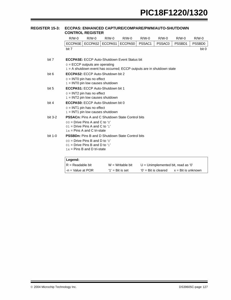
PIC18F1220/1320
REGISTER 15-3: ECCPAS: ENHANCED CAPTURE/COMPARE/PWM/AUTO-SHUTDOWN CONTROL REGISTER
R/W-0 R/W-0 R/W-0 R/W-0 R/W-0 R/W-0 R/W-0 R/W-0
ECCPASE ECCPAS2 ECCPAS1 ECCPAS0 PSSAC1 PSSAC0 PSSBD1 PSSBD0
bit 7 bit 0
bit 7 ECCPASE: ECCP Auto-Shutdown Event Status bit0 = ECCP outputs are operating 1 = A shutdown event has occurred; ECCP outputs are in shutdown state
bit 6 ECCPAS2: ECCP Auto-Shutdown bit 2
0 = INT0 pin has no effect 1 = INT0 pin low causes shutdown
bit 5 ECCPAS1: ECCP Auto-Shutdown bit 10 = INT2 pin has no effect 1 = INT2 pin low causes shutdown
bit 4 ECCPAS0: ECCP Auto-Shutdown bit 00 = INT1 pin has no effect 1 = INT1 pin low causes shutdown
bit 3-2 PSSACn: Pins A and C Shutdown State Control bits
00 = Drive Pins A and C to ‘0’01 = Drive Pins A and C to ‘1’1x = Pins A and C tri-state
bit 1-0 PSSBDn: Pins B and D Shutdown State Control bits00 = Drive Pins B and D to ‘0’01 = Drive Pins B and D to ‘1’1x = Pins B and D tri-state
Legend:
R = Readable bit W = Writable bit U = Unimplemented bit, read as ‘0’
-n = Value at POR ‘1’ = Bit is set ‘0’ = Bit is cleared x = Bit is unknown
2004 Microchip Technology Inc. DS39605C-page 127
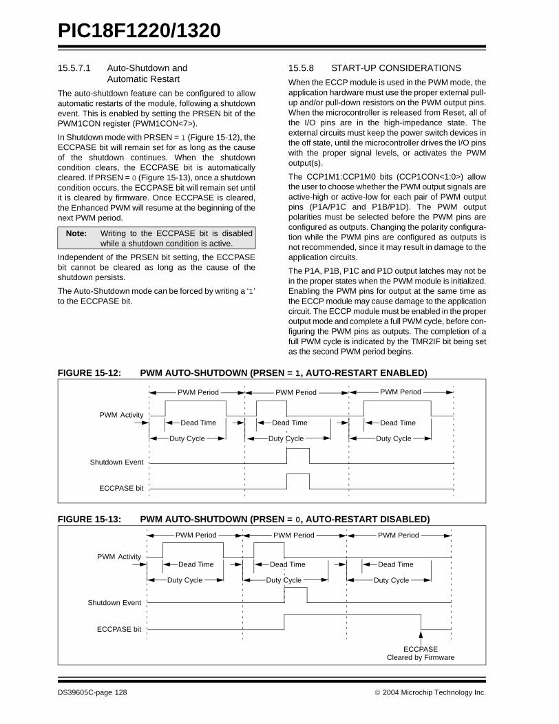
PIC18F1220/1320
15.5.7.1 Auto-Shutdown and Automatic Restart
The auto-shutdown feature can be configured to allowautomatic restarts of the module, following a shutdownevent. This is enabled by setting the PRSEN bit of thePWM1CON register (PWM1CON<7>).
In Shutdown mode with PRSEN = 1 (Figure 15-12), theECCPASE bit will remain set for as long as the causeof the shutdown continues. When the shutdowncondition clears, the ECCPASE bit is automaticallycleared. If PRSEN = 0 (Figure 15-13), once a shutdowncondition occurs, the ECCPASE bit will remain set untilit is cleared by firmware. Once ECCPASE is cleared,the Enhanced PWM will resume at the beginning of thenext PWM period.
Independent of the PRSEN bit setting, the ECCPASEbit cannot be cleared as long as the cause of theshutdown persists.
The Auto-Shutdown mode can be forced by writing a ‘1’to the ECCPASE bit.
15.5.8 START-UP CONSIDERATIONS
When the ECCP module is used in the PWM mode, theapplication hardware must use the proper external pull-up and/or pull-down resistors on the PWM output pins.When the microcontroller is released from Reset, all ofthe I/O pins are in the high-impedance state. Theexternal circuits must keep the power switch devices inthe off state, until the microcontroller drives the I/O pinswith the proper signal levels, or activates the PWMoutput(s).
The CCP1M1:CCP1M0 bits (CCP1CON<1:0>) allowthe user to choose whether the PWM output signals areactive-high or active-low for each pair of PWM outputpins (P1A/P1C and P1B/P1D). The PWM outputpolarities must be selected before the PWM pins areconfigured as outputs. Changing the polarity configura-tion while the PWM pins are configured as outputs isnot recommended, since it may result in damage to theapplication circuits.
The P1A, P1B, P1C and P1D output latches may not bein the proper states when the PWM module is initialized.Enabling the PWM pins for output at the same time asthe ECCP module may cause damage to the applicationcircuit. The ECCP module must be enabled in the properoutput mode and complete a full PWM cycle, before con-figuring the PWM pins as outputs. The completion of afull PWM cycle is indicated by the TMR2IF bit being setas the second PWM period begins.
FIGURE 15-12: PWM AUTO-SHUTDOWN (PRSEN = 1, AUTO-RESTART ENABLED)
FIGURE 15-13: PWM AUTO-SHUTDOWN (PRSEN = 0, AUTO-RESTART DISABLED)
Note: Writing to the ECCPASE bit is disabledwhile a shutdown condition is active.
Shutdown
PWM
ECCPASE bit
Activity
Event
PWM Period PWM Period PWM Period
Duty Cycle
Dead Time
Duty Cycle Duty Cycle
Dead TimeDead Time
Shutdown
PWM
ECCPASE bit
Activity
Event
PWM Period PWM Period PWM Period
ECCPASECleared by Firmware
Duty Cycle
Dead Time
Duty Cycle Duty Cycle
Dead TimeDead Time
DS39605C-page 128 2004 Microchip Technology Inc.
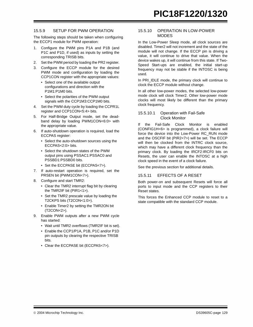
PIC18F1220/1320
15.5.9 SETUP FOR PWM OPERATION
The following steps should be taken when configuringthe ECCP1 module for PWM operation:
1. Configure the PWM pins P1A and P1B (andP1C and P1D, if used) as inputs by setting thecorresponding TRISB bits.
2. Set the PWM period by loading the PR2 register.3. Configure the ECCP module for the desired
PWM mode and configuration by loading theCCP1CON register with the appropriate values:
• Select one of the available output configurations and direction with the P1M1:P1M0 bits.
• Select the polarities of the PWM output signals with the CCP1M3:CCP1M0 bits.
4. Set the PWM duty cycle by loading the CCPR1Lregister and CCP1CON<5:4> bits.
5. For Half-Bridge Output mode, set the dead-band delay by loading PWM1CON<6:0> withthe appropriate value.
6. If auto-shutdown operation is required, load theECCPAS register:• Select the auto-shutdown sources using the
ECCPAS<2:0> bits.• Select the shutdown states of the PWM
output pins using PSSAC1:PSSAC0 and PSSBD1:PSSBD0 bits.
• Set the ECCPASE bit (ECCPAS<7>).7. If auto-restart operation is required, set the
PRSEN bit (PWM1CON<7>).8. Configure and start TMR2:
• Clear the TMR2 interrupt flag bit by clearing the TMR2IF bit (PIR1<1>).
• Set the TMR2 prescale value by loading the T2CKPS bits (T2CON<1:0>).
• Enable Timer2 by setting the TMR2ON bit (T2CON<2>).
9. Enable PWM outputs after a new PWM cyclehas started:• Wait until TMR2 overflows (TMR2IF bit is set).
• Enable the CCP1/P1A, P1B, P1C and/or P1D pin outputs by clearing the respective TRISB bits.
• Clear the ECCPASE bit (ECCPAS<7>).
15.5.10 OPERATION IN LOW-POWER MODES
In the Low-Power Sleep mode, all clock sources aredisabled. Timer2 will not increment and the state of themodule will not change. If the ECCP pin is driving avalue, it will continue to drive that value. When thedevice wakes up, it will continue from this state. If Two-Speed Start-ups are enabled, the initial start-upfrequency may not be stable if the INTOSC is beingused.
In PRI_IDLE mode, the primary clock will continue toclock the ECCP module without change.
In all other low-power modes, the selected low-powermode clock will clock Timer2. Other low-power modeclocks will most likely be different than the primaryclock frequency.
15.5.10.1 Operation with Fail-Safe Clock Monitor
If the Fail-Safe Clock Monitor is enabled(CONFIG1H<6> is programmed), a clock failure willforce the device into the Low-Power RC_RUN modeand the OSCFIF bit (PIR2<7>) will be set. The ECCPwill then be clocked from the INTRC clock source,which may have a different clock frequency than theprimary clock. By loading the IRCF2:IRCF0 bits onResets, the user can enable the INTOSC at a highclock speed in the event of a clock failure.
See the previous section for additional details.
15.5.11 EFFECTS OF A RESET
Both power-on and subsequent Resets will force allports to input mode and the CCP registers to theirReset states.
This forces the Enhanced CCP module to reset to astate compatible with the standard CCP module.
2004 Microchip Technology Inc. DS39605C-page 129
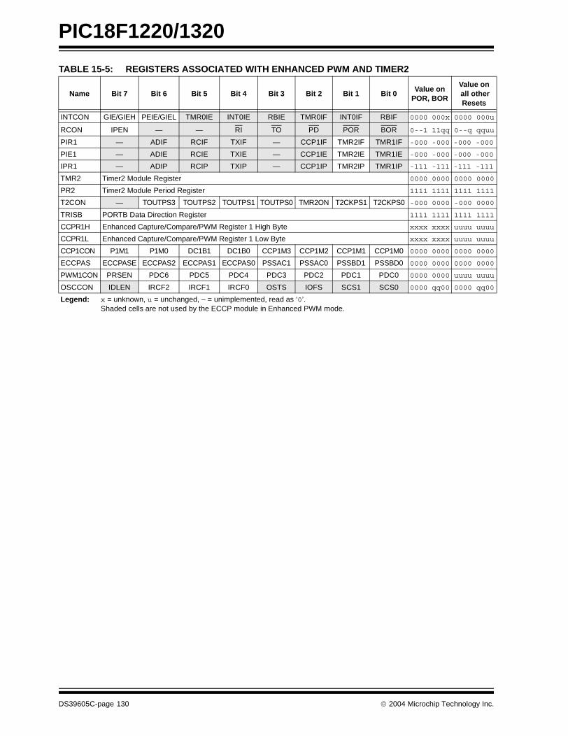
PIC18F1220/1320
TABLE 15-5: REGISTERS ASSOCIATED WITH ENHANCED PWM AND TIMER2
Name Bit 7 Bit 6 Bit 5 Bit 4 Bit 3 Bit 2 Bit 1 Bit 0Value on
POR, BOR
Value on all other Resets
INTCON GIE/GIEH PEIE/GIEL TMR0IE INT0IE RBIE TMR0IF INT0IF RBIF 0000 000x 0000 000u
RCON IPEN — — RI TO PD POR BOR 0--1 11qq 0--q qquu
PIR1 — ADIF RCIF TXIF — CCP1IF TMR2IF TMR1IF -000 -000 -000 -000
PIE1 — ADIE RCIE TXIE — CCP1IE TMR2IE TMR1IE -000 -000 -000 -000
IPR1 — ADIP RCIP TXIP — CCP1IP TMR2IP TMR1IP -111 -111 -111 -111
TMR2 Timer2 Module Register 0000 0000 0000 0000
PR2 Timer2 Module Period Register 1111 1111 1111 1111
T2CON — TOUTPS3 TOUTPS2 TOUTPS1 TOUTPS0 TMR2ON T2CKPS1 T2CKPS0 -000 0000 -000 0000
TRISB PORTB Data Direction Register 1111 1111 1111 1111
CCPR1H Enhanced Capture/Compare/PWM Register 1 High Byte xxxx xxxx uuuu uuuu
CCPR1L Enhanced Capture/Compare/PWM Register 1 Low Byte xxxx xxxx uuuu uuuu
CCP1CON P1M1 P1M0 DC1B1 DC1B0 CCP1M3 CCP1M2 CCP1M1 CCP1M0 0000 0000 0000 0000
ECCPAS ECCPASE ECCPAS2 ECCPAS1 ECCPAS0 PSSAC1 PSSAC0 PSSBD1 PSSBD0 0000 0000 0000 0000
PWM1CON PRSEN PDC6 PDC5 PDC4 PDC3 PDC2 PDC1 PDC0 0000 0000 uuuu uuuu
OSCCON IDLEN IRCF2 IRCF1 IRCF0 OSTS IOFS SCS1 SCS0 0000 qq00 0000 qq00
Legend: x = unknown, u = unchanged, – = unimplemented, read as ‘0’. Shaded cells are not used by the ECCP module in Enhanced PWM mode.
DS39605C-page 130 2004 Microchip Technology Inc.

PIC18F1220/1320
16.0 ENHANCED ADDRESSABLE UNIVERSAL SYNCHRONOUS ASYNCHRONOUS RECEIVER TRANSMITTER (EUSART)
The Enhanced Addressable Universal SynchronousAsynchronous Receiver Transmitter (EUSART) mod-ule can be configured as a full-duplex asynchronoussystem that can communicate with peripheral devices,such as CRT terminals and personal computers. It canalso be configured as a half-duplex synchronoussystem that can communicate with peripheral devices,such as A/D or D/A integrated circuits, serialEEPROMs, etc.
The Enhanced Addressable USART moduleimplements additional features, including automaticbaud rate detection and calibration, automatic wake-upon Sync Break reception and 12-bit Break charactertransmit. These features make it ideally suited for usein Local Interconnect Network (LIN) bus systems.
The EUSART can be configured in the followingmodes:
• Asynchronous (full duplex) with:- Auto-wake-up on character reception
- Auto-baud calibration- 12-bit Break character transmission
• Synchronous – Master (half duplex) with selectable clock polarity
• Synchronous – Slave (half duplex) with selectable clock polarity
The RB1/AN5/TX/CK/INT1 and RB4/AN6/RX/DT/KBI0pins must be configured as follows for use with theUniversal Synchronous Asynchronous ReceiverTransmitter:
• SPEN (RCSTA<7>) bit must be set ( = 1), • PCFG6:PCFG5 (ADCON1<5:6>) must be set ( = 1),
• TRISB<4> bit must be set ( = 1) and• TRISB<1> bit must be set ( = 1).
The operation of the Enhanced USART module iscontrolled through three registers:
• Transmit Status and Control (TXSTA)• Receive Status and Control (RCSTA)
• Baud Rate Control (BAUDCTL)
These are detailed in on the following pages inRegister 16-1, Register 16-2 and Register 16-3,respectively.
16.1 Asynchronous Operation in Power Managed Modes
The EUSART may operate in Asynchronous modewhile the peripheral clocks are being provided by theinternal oscillator block. This makes it possible toremove the crystal or resonator that is commonlyconnected as the primary clock on the OSC1 andOSC2 pins.
The factory calibrates the internal oscillator block out-put (INTOSC) for 8 MHz (see Table 22-6). However,this frequency may drift as VDD or temperaturechanges and this directly affects the asynchronousbaud rate. Two methods may be used to adjust thebaud rate clock, but both require a reference clocksource of some kind.
The first (preferred) method uses the OSCTUNEregister to adjust the INTOSC output back to 8 MHz.Adjusting the value in the OSCTUNE register allows forfine resolution changes to the system clock source (seeSection 3.6 “INTOSC Frequency Drift” for moreinformation).
The other method adjusts the value in the Baud RateGenerator (BRG). There may not be fine enoughresolution when adjusting the Baud Rate Generator tocompensate for a gradual change in the peripheralclock frequency.
Note: The EUSART control will automaticallyreconfigure the pin from input to output asneeded.
2004 Microchip Technology Inc. DS39605C-page 131
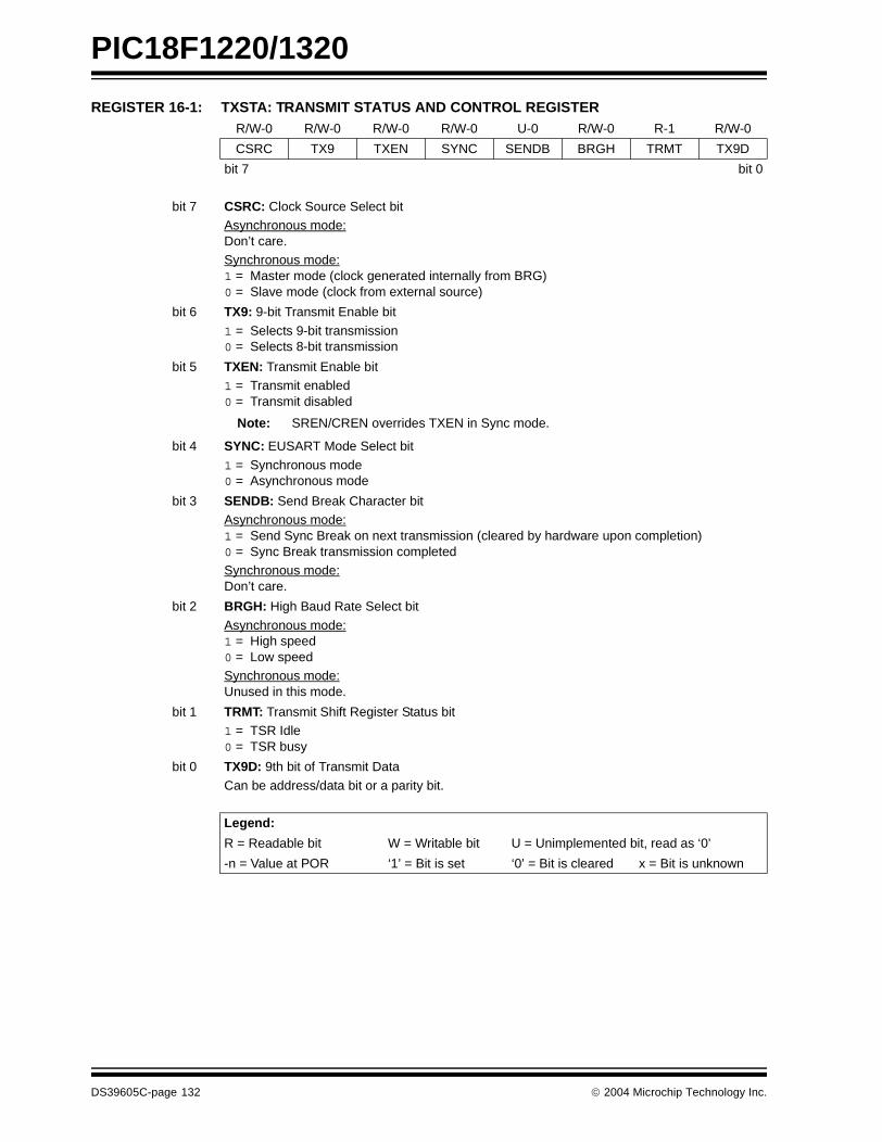
PIC18F1220/1320
REGISTER 16-1: TXSTA: TRANSMIT STATUS AND CONTROL REGISTER R/W-0 R/W-0 R/W-0 R/W-0 U-0 R/W-0 R-1 R/W-0
CSRC TX9 TXEN SYNC SENDB BRGH TRMT TX9D
bit 7 bit 0
bit 7 CSRC: Clock Source Select bitAsynchronous mode: Don’t care.Synchronous mode: 1 = Master mode (clock generated internally from BRG)0 = Slave mode (clock from external source)
bit 6 TX9: 9-bit Transmit Enable bit
1 = Selects 9-bit transmission 0 = Selects 8-bit transmission
bit 5 TXEN: Transmit Enable bit 1 = Transmit enabled0 = Transmit disabled
Note: SREN/CREN overrides TXEN in Sync mode.
bit 4 SYNC: EUSART Mode Select bit
1 = Synchronous mode 0 = Asynchronous mode
bit 3 SENDB: Send Break Character bitAsynchronous mode:1 = Send Sync Break on next transmission (cleared by hardware upon completion)0 = Sync Break transmission completedSynchronous mode:Don’t care.
bit 2 BRGH: High Baud Rate Select bit
Asynchronous mode: 1 = High speed 0 = Low speedSynchronous mode: Unused in this mode.
bit 1 TRMT: Transmit Shift Register Status bit1 = TSR Idle 0 = TSR busy
bit 0 TX9D: 9th bit of Transmit Data
Can be address/data bit or a parity bit.
Legend:
R = Readable bit W = Writable bit U = Unimplemented bit, read as ‘0’
-n = Value at POR ‘1’ = Bit is set ‘0’ = Bit is cleared x = Bit is unknown
DS39605C-page 132 2004 Microchip Technology Inc.
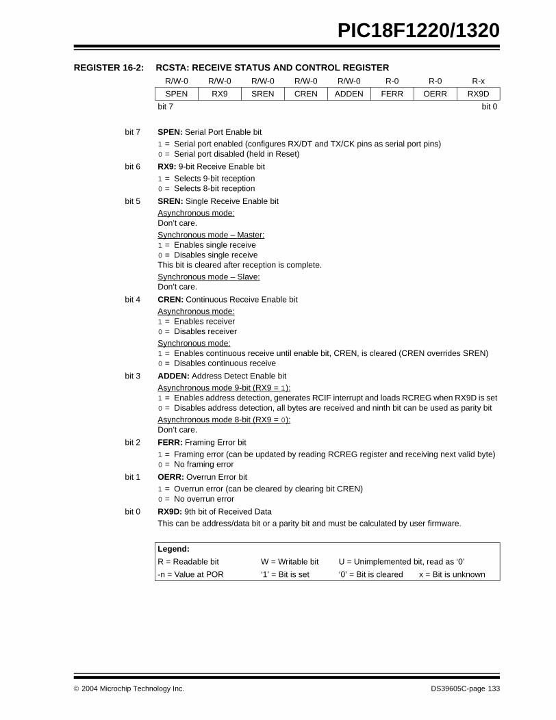
PIC18F1220/1320
REGISTER 16-2: RCSTA: RECEIVE STATUS AND CONTROL REGISTER R/W-0 R/W-0 R/W-0 R/W-0 R/W-0 R-0 R-0 R-x
SPEN RX9 SREN CREN ADDEN FERR OERR RX9D
bit 7 bit 0
bit 7 SPEN: Serial Port Enable bit1 = Serial port enabled (configures RX/DT and TX/CK pins as serial port pins)0 = Serial port disabled (held in Reset)
bit 6 RX9: 9-bit Receive Enable bit
1 = Selects 9-bit reception 0 = Selects 8-bit reception
bit 5 SREN: Single Receive Enable bit Asynchronous mode: Don’t care.Synchronous mode – Master: 1 = Enables single receive0 = Disables single receive This bit is cleared after reception is complete.
Synchronous mode – Slave: Don’t care.
bit 4 CREN: Continuous Receive Enable bit Asynchronous mode: 1 = Enables receiver0 = Disables receiverSynchronous mode: 1 = Enables continuous receive until enable bit, CREN, is cleared (CREN overrides SREN) 0 = Disables continuous receive
bit 3 ADDEN: Address Detect Enable bitAsynchronous mode 9-bit (RX9 = 1):1 = Enables address detection, generates RCIF interrupt and loads RCREG when RX9D is set0 = Disables address detection, all bytes are received and ninth bit can be used as parity bitAsynchronous mode 8-bit (RX9 = 0):Don’t care.
bit 2 FERR: Framing Error bit
1 = Framing error (can be updated by reading RCREG register and receiving next valid byte)0 = No framing error
bit 1 OERR: Overrun Error bit 1 = Overrun error (can be cleared by clearing bit CREN) 0 = No overrun error
bit 0 RX9D: 9th bit of Received Data This can be address/data bit or a parity bit and must be calculated by user firmware.
Legend:
R = Readable bit W = Writable bit U = Unimplemented bit, read as ‘0’
-n = Value at POR ‘1’ = Bit is set ‘0’ = Bit is cleared x = Bit is unknown
2004 Microchip Technology Inc. DS39605C-page 133
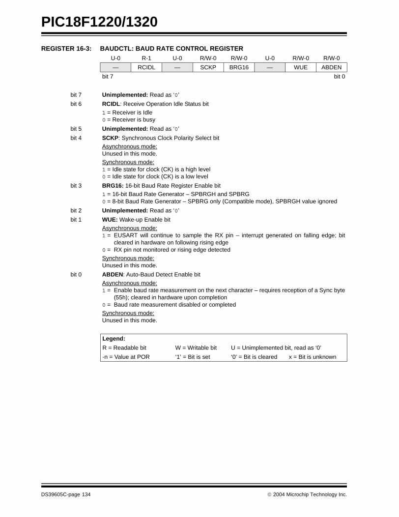
PIC18F1220/1320
REGISTER 16-3: BAUDCTL: BAUD RATE CONTROL REGISTER U-0 R-1 U-0 R/W-0 R/W-0 U-0 R/W-0 R/W-0
— RCIDL — SCKP BRG16 — WUE ABDEN
bit 7 bit 0
bit 7 Unimplemented: Read as ‘0’
bit 6 RCIDL: Receive Operation Idle Status bit
1 = Receiver is Idle0 = Receiver is busy
bit 5 Unimplemented: Read as ‘0’
bit 4 SCKP: Synchronous Clock Polarity Select bitAsynchronous mode:Unused in this mode. Synchronous mode:1 = Idle state for clock (CK) is a high level0 = Idle state for clock (CK) is a low level
bit 3 BRG16: 16-bit Baud Rate Register Enable bit1 = 16-bit Baud Rate Generator – SPBRGH and SPBRG0 = 8-bit Baud Rate Generator – SPBRG only (Compatible mode), SPBRGH value ignored
bit 2 Unimplemented: Read as ‘0’
bit 1 WUE: Wake-up Enable bit
Asynchronous mode:1 = EUSART will continue to sample the RX pin – interrupt generated on falling edge; bit
cleared in hardware on following rising edge0 = RX pin not monitored or rising edge detectedSynchronous mode:Unused in this mode.
bit 0 ABDEN: Auto-Baud Detect Enable bit
Asynchronous mode:1 = Enable baud rate measurement on the next character – requires reception of a Sync byte
(55h); cleared in hardware upon completion0 = Baud rate measurement disabled or completedSynchronous mode:Unused in this mode.
Legend:
R = Readable bit W = Writable bit U = Unimplemented bit, read as ‘0’
-n = Value at POR ‘1’ = Bit is set ‘0’ = Bit is cleared x = Bit is unknown
DS39605C-page 134 2004 Microchip Technology Inc.
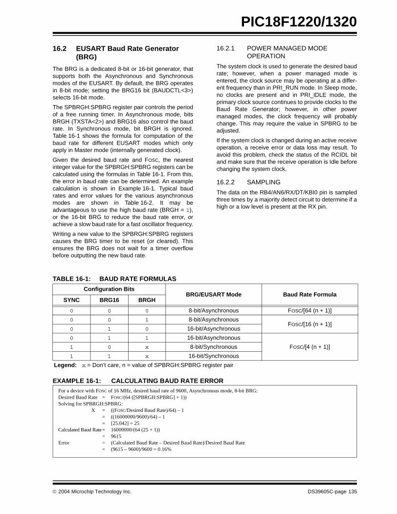
PIC18F1220/1320
16.2 EUSART Baud Rate Generator (BRG)
The BRG is a dedicated 8-bit or 16-bit generator, thatsupports both the Asynchronous and Synchronousmodes of the EUSART. By default, the BRG operatesin 8-bit mode; setting the BRG16 bit (BAUDCTL<3>)selects 16-bit mode.
The SPBRGH:SPBRG register pair controls the periodof a free running timer. In Asynchronous mode, bitsBRGH (TXSTA<2>) and BRG16 also control the baudrate. In Synchronous mode, bit BRGH is ignored.Table 16-1 shows the formula for computation of thebaud rate for different EUSART modes which onlyapply in Master mode (internally generated clock).
Given the desired baud rate and FOSC, the nearestinteger value for the SPBRGH:SPBRG registers can becalculated using the formulas in Table 16-1. From this,the error in baud rate can be determined. An examplecalculation is shown in Example 16-1. Typical baudrates and error values for the various asynchronousmodes are shown in Table 16-2. It may beadvantageous to use the high baud rate (BRGH = 1),or the 16-bit BRG to reduce the baud rate error, orachieve a slow baud rate for a fast oscillator frequency.
Writing a new value to the SPBRGH:SPBRG registerscauses the BRG timer to be reset (or cleared). Thisensures the BRG does not wait for a timer overflowbefore outputting the new baud rate.
16.2.1 POWER MANAGED MODE OPERATION
The system clock is used to generate the desired baudrate; however, when a power managed mode isentered, the clock source may be operating at a differ-ent frequency than in PRI_RUN mode. In Sleep mode,no clocks are present and in PRI_IDLE mode, theprimary clock source continues to provide clocks to theBaud Rate Generator; however, in other powermanaged modes, the clock frequency will probablychange. This may require the value in SPBRG to beadjusted.
If the system clock is changed during an active receiveoperation, a receive error or data loss may result. Toavoid this problem, check the status of the RCIDL bitand make sure that the receive operation is Idle beforechanging the system clock.
16.2.2 SAMPLING
The data on the RB4/AN6/RX/DT/KBI0 pin is sampledthree times by a majority detect circuit to determine if ahigh or a low level is present at the RX pin.
TABLE 16-1: BAUD RATE FORMULAS
EXAMPLE 16-1: CALCULATING BAUD RATE ERROR
Configuration BitsBRG/EUSART Mode Baud Rate Formula
SYNC BRG16 BRGH
0 0 0 8-bit/Asynchronous FOSC/[64 (n + 1)]
0 0 1 8-bit/AsynchronousFOSC/[16 (n + 1)]
0 1 0 16-bit/Asynchronous
0 1 1 16-bit/Asynchronous
FOSC/[4 (n + 1)]1 0 x 8-bit/Synchronous
1 1 x 16-bit/Synchronous
Legend: x = Don’t care, n = value of SPBRGH:SPBRG register pair
For a device with FOSC of 16 MHz, desired baud rate of 9600, Asynchronous mode, 8-bit BRG:Desired Baud Rate = FOSC/(64 ([SPBRGH:SPBRG] + 1)) Solving for SPBRGH:SPBRG:
X = ((FOSC/Desired Baud Rate)/64) – 1= ((16000000/9600)/64) – 1 = [25.042] = 25
Calculated Baud Rate= 16000000/(64 (25 + 1)) = 9615
Error = (Calculated Baud Rate – Desired Baud Rate)/Desired Baud Rate= (9615 – 9600)/9600 = 0.16%
2004 Microchip Technology Inc. DS39605C-page 135
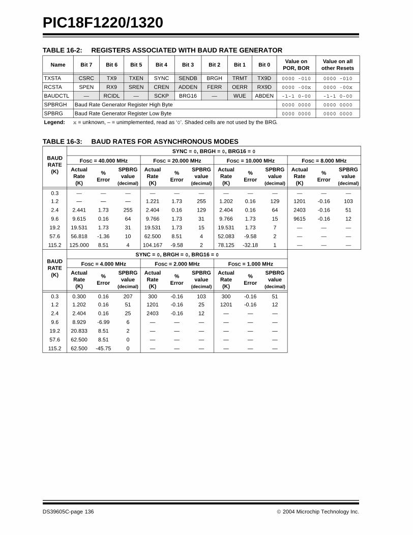
PIC18F1220/1320
TABLE 16-2: REGISTERS ASSOCIATED WITH BAUD RATE GENERATOR
Name Bit 7 Bit 6 Bit 5 Bit 4 Bit 3 Bit 2 Bit 1 Bit 0Value on
POR, BORValue on allother Resets
TXSTA CSRC TX9 TXEN SYNC SENDB BRGH TRMT TX9D 0000 -010 0000 -010
RCSTA SPEN RX9 SREN CREN ADDEN FERR OERR RX9D 0000 -00x 0000 -00x
BAUDCTL — RCIDL — SCKP BRG16 — WUE ABDEN -1-1 0-00 -1-1 0-00
SPBRGH Baud Rate Generator Register High Byte 0000 0000 0000 0000
SPBRG Baud Rate Generator Register Low Byte 0000 0000 0000 0000
Legend: x = unknown, – = unimplemented, read as ‘0’. Shaded cells are not used by the BRG.
TABLE 16-3: BAUD RATES FOR ASYNCHRONOUS MODES
BAUDRATE
(K)
SYNC = 0, BRGH = 0, BRG16 = 0
FOSC = 40.000 MHz FOSC = 20.000 MHz FOSC = 10.000 MHz FOSC = 8.000 MHz
Actual Rate (K)
%Error
SPBRGvalue
(decimal)
Actual Rate (K)
%Error
SPBRGvalue
(decimal)
Actual Rate (K)
%Error
SPBRGvalue
(decimal)
Actual Rate (K)
%Error
SPBRGvalue
(decimal)
0.3 — — — — — — — — — — — —
1.2 — — — 1.221 1.73 255 1.202 0.16 129 1201 -0.16 103
2.4 2.441 1.73 255 2.404 0.16 129 2.404 0.16 64 2403 -0.16 51
9.6 9.615 0.16 64 9.766 1.73 31 9.766 1.73 15 9615 -0.16 12
19.2 19.531 1.73 31 19.531 1.73 15 19.531 1.73 7 — — —
57.6 56.818 -1.36 10 62.500 8.51 4 52.083 -9.58 2 — — —
115.2 125.000 8.51 4 104.167 -9.58 2 78.125 -32.18 1 — — —
BAUDRATE
(K)
SYNC = 0, BRGH = 0, BRG16 = 0
FOSC = 4.000 MHz FOSC = 2.000 MHz FOSC = 1.000 MHz
Actual Rate (K)
%Error
SPBRGvalue
(decimal)
Actual Rate (K)
%Error
SPBRGvalue
(decimal)
Actual Rate (K)
%Error
SPBRGvalue
(decimal)
0.3 0.300 0.16 207 300 -0.16 103 300 -0.16 51
1.2 1.202 0.16 51 1201 -0.16 25 1201 -0.16 12
2.4 2.404 0.16 25 2403 -0.16 12 — — —
9.6 8.929 -6.99 6 — — — — — —
19.2 20.833 8.51 2 — — — — — —
57.6 62.500 8.51 0 — — — — — —
115.2 62.500 -45.75 0 — — — — — —
DS39605C-page 136 2004 Microchip Technology Inc.

PIC18F1220/1320
BAUDRATE
(K)
SYNC = 0, BRGH = 1, BRG16 = 0
FOSC = 40.000 MHz FOSC = 20.000 MHz FOSC = 10.000 MHz FOSC = 8.000 MHz
Actual Rate (K)
%Error
SPBRGvalue
(decimal)
Actual Rate (K)
%Error
SPBRGvalue
(decimal)
Actual Rate (K)
%Error
SPBRGvalue
(decimal)
Actual Rate (K)
%Error
SPBRGvalue
(decimal)
2.4 — — — — — — 2.441 1.73 255 2403 -0.16 207
9.6 9.766 1.73 255 9.615 0.16 129 9.615 0.16 64 9615 -0.16 51
19.2 19.231 0.16 129 19.231 0.16 64 19.531 1.73 31 19230 -0.16 25
57.6 58.140 0.94 42 56.818 -1.36 21 56.818 -1.36 10 55555 3.55 8
115.2 113.636 -1.36 21 113.636 -1.36 10 125.000 8.51 4 — — —
BAUDRATE
(K)
SYNC = 0, BRGH = 1, BRG16 = 0
FOSC = 4.000 MHz FOSC = 2.000 MHz FOSC = 1.000 MHz
Actual Rate (K)
%Error
SPBRGvalue
(decimal)
Actual Rate (K)
%Error
SPBRGvalue
(decimal)
Actual Rate (K)
%Error
SPBRGvalue
(decimal)
0.3 — — — — — — 300 -0.16 207
1.2 1.202 0.16 207 1201 -0.16 103 1201 -0.16 51
2.4 2.404 0.16 103 2403 -0.16 51 2403 -0.16 25
9.6 9.615 0.16 25 9615 -0.16 12 — — —
19.2 19.231 0.16 12 — — — — — —
57.6 62.500 8.51 3 — — — — — —
115.2 125.000 8.51 1 — — — — — —
BAUDRATE
(K)
SYNC = 0, BRGH = 0, BRG16 = 1
FOSC = 40.000 MHz FOSC = 20.000 MHz FOSC = 10.000 MHz FOSC = 8.000 MHz
Actual Rate (K)
%Error
SPBRGvalue
(decimal)
Actual Rate (K)
%Error
SPBRGvalue
(decimal)
Actual Rate (K)
%Error
SPBRGvalue
(decimal)
Actual Rate (K)
%Error
SPBRGvalue
(decimal)
0.3 0.300 0.00 8332 0.300 0.02 4165 0.300 0.02 2082 300 -0.04 1665
1.2 1.200 0.02 2082 1.200 -0.03 1041 1.200 -0.03 520 1201 -0.16 415
2.4 2.402 0.06 1040 2.399 -0.03 520 2.404 0.16 259 2403 -0.16 207
9.6 9.615 0.16 259 9.615 0.16 129 9.615 0.16 64 9615 -0.16 51
19.2 19.231 0.16 129 19.231 0.16 64 19.531 1.73 31 19230 -0.16 25
57.6 58.140 0.94 42 56.818 -1.36 21 56.818 -1.36 10 55555 3.55 8
115.2 113.636 -1.36 21 113.636 -1.36 10 125.000 8.51 4 — — —
BAUDRATE
(K)
SYNC = 0, BRGH = 0, BRG16 = 1
FOSC = 4.000 MHz FOSC = 2.000 MHz FOSC = 1.000 MHz
Actual Rate (K)
%Error
SPBRGvalue
(decimal)
Actual Rate (K)
%Error
SPBRGvalue
(decimal)
Actual Rate (K)
%Error
SPBRGvalue
(decimal)
0.3 0.300 0.04 832 300 -0.16 415 300 -0.16 207
1.2 1.202 0.16 207 1201 -0.16 103 1201 -0.16 51
2.4 2.404 0.16 103 2403 -0.16 51 2403 -0.16 25
9.6 9.615 0.16 25 9615 -0.16 12 — — —
19.2 19.231 0.16 12 — — — — — —
57.6 62.500 8.51 3 — — — — — —
115.2 125.000 8.51 1 — — — — — —
TABLE 16-3: BAUD RATES FOR ASYNCHRONOUS MODES (CONTINUED)
2004 Microchip Technology Inc. DS39605C-page 137
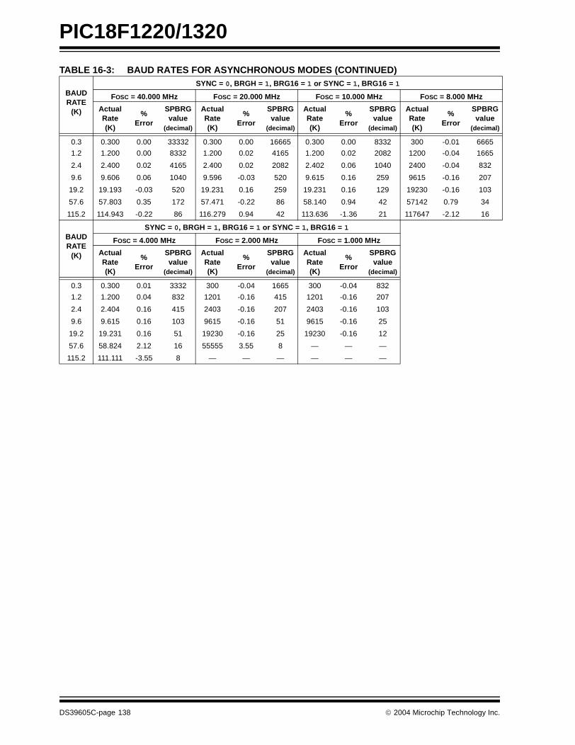
PIC18F1220/1320
BAUDRATE
(K)
SYNC = 0, BRGH = 1, BRG16 = 1 or SYNC = 1, BRG16 = 1
FOSC = 40.000 MHz FOSC = 20.000 MHz FOSC = 10.000 MHz FOSC = 8.000 MHz
Actual Rate (K)
%Error
SPBRGvalue
(decimal)
Actual Rate (K)
%Error
SPBRGvalue
(decimal)
Actual Rate (K)
%Error
SPBRGvalue
(decimal)
Actual Rate (K)
%Error
SPBRGvalue
(decimal)
0.3 0.300 0.00 33332 0.300 0.00 16665 0.300 0.00 8332 300 -0.01 6665
1.2 1.200 0.00 8332 1.200 0.02 4165 1.200 0.02 2082 1200 -0.04 1665
2.4 2.400 0.02 4165 2.400 0.02 2082 2.402 0.06 1040 2400 -0.04 832
9.6 9.606 0.06 1040 9.596 -0.03 520 9.615 0.16 259 9615 -0.16 207
19.2 19.193 -0.03 520 19.231 0.16 259 19.231 0.16 129 19230 -0.16 103
57.6 57.803 0.35 172 57.471 -0.22 86 58.140 0.94 42 57142 0.79 34
115.2 114.943 -0.22 86 116.279 0.94 42 113.636 -1.36 21 117647 -2.12 16
BAUDRATE
(K)
SYNC = 0, BRGH = 1, BRG16 = 1 or SYNC = 1, BRG16 = 1
FOSC = 4.000 MHz FOSC = 2.000 MHz FOSC = 1.000 MHz
Actual Rate (K)
%Error
SPBRGvalue
(decimal)
Actual Rate (K)
%Error
SPBRGvalue
(decimal)
Actual Rate (K)
%Error
SPBRGvalue
(decimal)
0.3 0.300 0.01 3332 300 -0.04 1665 300 -0.04 832
1.2 1.200 0.04 832 1201 -0.16 415 1201 -0.16 207
2.4 2.404 0.16 415 2403 -0.16 207 2403 -0.16 103
9.6 9.615 0.16 103 9615 -0.16 51 9615 -0.16 25
19.2 19.231 0.16 51 19230 -0.16 25 19230 -0.16 12
57.6 58.824 2.12 16 55555 3.55 8 — — —
115.2 111.111 -3.55 8 — — — — — —
TABLE 16-3: BAUD RATES FOR ASYNCHRONOUS MODES (CONTINUED)
DS39605C-page 138 2004 Microchip Technology Inc.
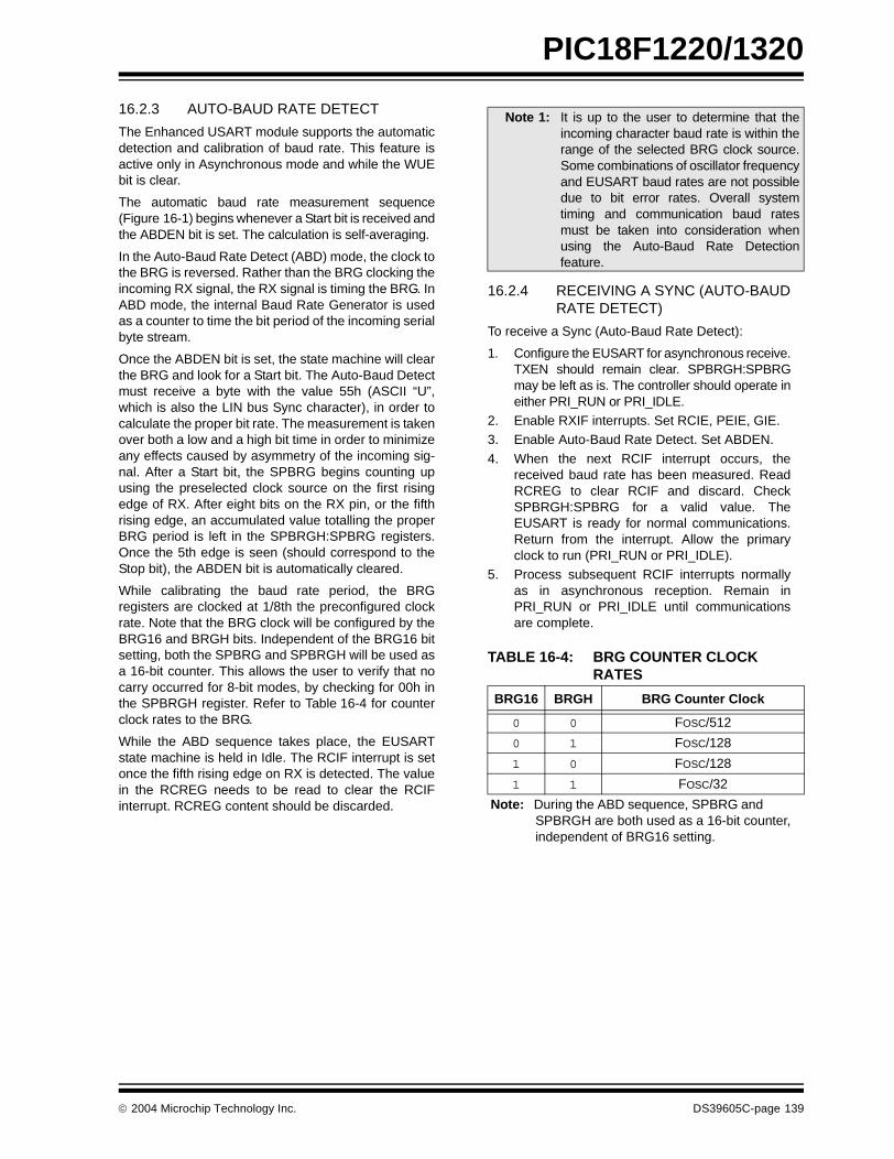
PIC18F1220/1320
16.2.3 AUTO-BAUD RATE DETECT
The Enhanced USART module supports the automaticdetection and calibration of baud rate. This feature isactive only in Asynchronous mode and while the WUEbit is clear.
The automatic baud rate measurement sequence(Figure 16-1) begins whenever a Start bit is received andthe ABDEN bit is set. The calculation is self-averaging.
In the Auto-Baud Rate Detect (ABD) mode, the clock tothe BRG is reversed. Rather than the BRG clocking theincoming RX signal, the RX signal is timing the BRG. InABD mode, the internal Baud Rate Generator is usedas a counter to time the bit period of the incoming serialbyte stream.
Once the ABDEN bit is set, the state machine will clearthe BRG and look for a Start bit. The Auto-Baud Detectmust receive a byte with the value 55h (ASCII “U”,which is also the LIN bus Sync character), in order tocalculate the proper bit rate. The measurement is takenover both a low and a high bit time in order to minimizeany effects caused by asymmetry of the incoming sig-nal. After a Start bit, the SPBRG begins counting upusing the preselected clock source on the first risingedge of RX. After eight bits on the RX pin, or the fifthrising edge, an accumulated value totalling the properBRG period is left in the SPBRGH:SPBRG registers.Once the 5th edge is seen (should correspond to theStop bit), the ABDEN bit is automatically cleared.
While calibrating the baud rate period, the BRGregisters are clocked at 1/8th the preconfigured clockrate. Note that the BRG clock will be configured by theBRG16 and BRGH bits. Independent of the BRG16 bitsetting, both the SPBRG and SPBRGH will be used asa 16-bit counter. This allows the user to verify that nocarry occurred for 8-bit modes, by checking for 00h inthe SPBRGH register. Refer to Table 16-4 for counterclock rates to the BRG.
While the ABD sequence takes place, the EUSARTstate machine is held in Idle. The RCIF interrupt is setonce the fifth rising edge on RX is detected. The valuein the RCREG needs to be read to clear the RCIFinterrupt. RCREG content should be discarded.
16.2.4 RECEIVING A SYNC (AUTO-BAUD RATE DETECT)
To receive a Sync (Auto-Baud Rate Detect):
1. Configure the EUSART for asynchronous receive.TXEN should remain clear. SPBRGH:SPBRGmay be left as is. The controller should operate ineither PRI_RUN or PRI_IDLE.
2. Enable RXIF interrupts. Set RCIE, PEIE, GIE.3. Enable Auto-Baud Rate Detect. Set ABDEN.
4. When the next RCIF interrupt occurs, thereceived baud rate has been measured. ReadRCREG to clear RCIF and discard. CheckSPBRGH:SPBRG for a valid value. TheEUSART is ready for normal communications.Return from the interrupt. Allow the primaryclock to run (PRI_RUN or PRI_IDLE).
5. Process subsequent RCIF interrupts normallyas in asynchronous reception. Remain inPRI_RUN or PRI_IDLE until communicationsare complete.
TABLE 16-4: BRG COUNTER CLOCK RATES
Note 1: It is up to the user to determine that theincoming character baud rate is within therange of the selected BRG clock source.Some combinations of oscillator frequencyand EUSART baud rates are not possibledue to bit error rates. Overall systemtiming and communication baud ratesmust be taken into consideration whenusing the Auto-Baud Rate Detectionfeature.
BRG16 BRGH BRG Counter Clock
0 0 FOSC/512
0 1 FOSC/128
1 0 FOSC/128
1 1 FOSC/32
Note: During the ABD sequence, SPBRG and SPBRGH are both used as a 16-bit counter, independent of BRG16 setting.
2004 Microchip Technology Inc. DS39605C-page 139

PIC18F1220/1320
FIGURE 16-1: AUTOMATIC BAUD RATE CALCULATION
16.3 EUSART Asynchronous Mode
The Asynchronous mode of operation is selected byclearing the SYNC bit (TXSTA<4>). In this mode, theEUSART uses standard Non-Return-to-Zero (NRZ) for-mat (one Start bit, eight or nine data bits and one Stopbit). The most common data format is 8 bits. An on-chipdedicated 8-bit/16-bit Baud Rate Generator can beused to derive standard baud rate frequencies from theoscillator.
The EUSART transmits and receives the LSb first. TheEUSART’s transmitter and receiver are functionallyindependent, but use the same data format and baudrate. The Baud Rate Generator produces a clock, eitherx16 or x64 of the bit shift rate, depending on the BRGHand BRG16 bits (TXSTA<2> and BAUDCTL<3>). Parityis not supported by the hardware, but can beimplemented in software and stored as the 9th data bit.
Asynchronous mode is available in all low-powermodes; it is available in Sleep mode only when auto-wake-up on Sync Break is enabled. When in PRI_IDLEmode, no changes to the Baud Rate Generator valuesare required; however, other low-power mode clocksmay operate at another frequency than the primaryclock. Therefore, the Baud Rate Generator values mayneed to be adjusted.
When operating in Asynchronous mode, the EUSARTmodule consists of the following important elements:
• Baud Rate Generator• Sampling Circuit• Asynchronous Transmitter
• Asynchronous Receiver• Auto-Wake-up on Sync Break Character• 12-bit Break Character Transmit
• Auto-Baud Rate Detection
16.3.1 EUSART ASYNCHRONOUS TRANSMITTER
The EUSART transmitter block diagram is shown inFigure 16-2. The heart of the transmitter is the Transmit(Serial) Shift Register (TSR). The shift register obtainsits data from the Read/Write Transmit Buffer register,TXREG. The TXREG register is loaded with data insoftware. The TSR register is not loaded until the Stopbit has been transmitted from the previous load. Assoon as the Stop bit is transmitted, the TSR is loadedwith new data from the TXREG register (if available).
Once the TXREG register transfers the data to the TSRregister (occurs in one TCY), the TXREG register isempty and flag bit, TXIF (PIR1<4>), is set. This interruptcan be enabled/disabled by setting/clearing enable bit,TXIE (PIE1<4>). Flag bit, TXIF, will be set, regardless ofthe state of enable bit, TXIE, and cannot be cleared insoftware. Flag bit, TXIF, is not cleared immediately uponloading the Transmit Buffer register, TXREG. TXIFbecomes valid in the second instruction cycle followingthe load instruction. Polling TXIF immediately following aload of TXREG will return invalid results.
While flag bit, TXIF, indicates the status of the TXREGregister, another bit, TRMT (TXSTA<1>), shows thestatus of the TSR register. Status bit, TRMT, is a read-only bit, which is set when the TSR register is empty.No interrupt logic is tied to this bit, so the user has topoll this bit in order to determine if the TSR register isempty.
BRG Value
RX pin
ABDEN bit
RCIF bit
Bit 0 Bit 1
(Interrupt)
ReadRCREG
BRG Clock
Start
Auto-ClearedSet by User
XXXXh 0000h
Edge #1
Bit 2 Bit 3Edge #2
Bit 4 Bit 5Edge #3
Bit 6 Bit 7Edge #4 Edge #5
001Ch
Note 1: The ABD sequence requires the EUSART module to be configured in Asynchronous mode and WUE = 0.
SPBRG XXXXh 1Ch
SPBRGH XXXXh 00h
Stop Bit
Note 1: The TSR register is not mapped in datamemory, so it is not available to the user.
2: Flag bit, TXIF, is set when enable bit,TXEN, is set.
DS39605C-page 140 2004 Microchip Technology Inc.

PIC18F1220/1320
To set up an Asynchronous Transmission:
1. Initialize the SPBRGH:SPBRG registers for theappropriate baud rate. Set or clear the BRGHand BRG16 bits, as required, to achieve thedesired baud rate.
2. Enable the asynchronous serial port by clearingbit SYNC and setting bit SPEN.
3. If interrupts are desired, set enable bit TXIE.
4. If 9-bit transmission is desired, set transmit bitTX9. Can be used as address/data bit.
5. Enable the transmission by setting bit TXEN,which will also set bit TXIF.
6. If 9-bit transmission is selected, the ninth bitshould be loaded in bit TX9D.
7. Load data to the TXREG register (startstransmission).
If using interrupts, ensure that the GIE and PEIE bits inthe INTCON register (INTCON<7:6>) are set.
FIGURE 16-2: EUSART TRANSMIT BLOCK DIAGRAM
FIGURE 16-3: ASYNCHRONOUS TRANSMISSION
TXIFTXIE
Interrupt
TXEN Baud Rate CLK
SPBRG
Baud Rate GeneratorTX9D
MSb LSb
Data Bus
TXREG Register
TSR Register
(8) 0
TX9
TRMT SPEN
RB1/AN5/TX/CK/INT1 pin
Pin Bufferand Control
8
• • •
SPBRGHBRG16
Word 1
Word 1Transmit Shift Reg
Start bit bit 0 bit 1 bit 7/8
Write to TXREGWord 1
BRG Output(Shift Clock)
RB1/AN5/TX/
TXIF bit(Transmit Buffer
Reg. Empty Flag)
TRMT bit(Transmit Shift
Reg. Empty Flag)
1 TCY
CK/INT1 (pin) Stop bit
2004 Microchip Technology Inc. DS39605C-page 141

PIC18F1220/1320
FIGURE 16-4: ASYNCHRONOUS TRANSMISSION (BACK TO BACK)
TABLE 16-5: REGISTERS ASSOCIATED WITH ASYNCHRONOUS TRANSMISSION
Transmit Shift Reg.
Write to TXREG
BRG Output(Shift Clock)
RB1/AN5/TX/
TXIF bit(Interrupt Reg. Flag)
TRMT bit(Transmit Shift
Reg. Empty Flag)
Word 1 Word 2
Word 1 Word 2
Stop bit Start bit
Transmit Shift Reg.
Word 1 Word 2bit 0 bit 1 bit 7/8 bit 0
Note: This timing diagram shows two consecutive transmissions.
1 TCY
1 TCY
CK/INT1 (pin) Start bit
Name Bit 7 Bit 6 Bit 5 Bit 4 Bit 3 Bit 2 Bit 1 Bit 0Value on
POR, BOR
Value onall otherResets
INTCON GIE/GIEH PEIE/GIEL TMR0IE INT0IE RBIE TMR0IF INT0IF RBIF 0000 000x 0000 000u
PIR1 — ADIF RCIF TXIF — CCP1IF TMR2IF TMR1IF -000 -000 -000 -000
PIE1 — ADIE RCIE TXIE — CCP1IE TMR2IE TMR1IE -000 -000 -000 -000
IPR1 — ADIP RCIP TXIP — CCP1IP TMR2IP TMR1IP -111 -111 -111 -111
RCSTA SPEN RX9 SREN CREN ADDEN FERR OERR RX9D 0000 -00x 0000 -00x
TXREG EUSART Transmit Register 0000 0000 0000 0000
TXSTA CSRC TX9 TXEN SYNC SENDB BRGH TRMT TX9D 0000 0010 0000 0010
BAUDCTL — RCIDL — SCKP BRG16 — WUE ABDEN -1-1 0-00 -1-1 0-00
SPBRGH Baud Rate Generator Register High Byte 0000 0000 0000 0000
SPBRG Baud Rate Generator Register Low Byte 0000 0000 0000 0000
Legend: x = unknown, – = unimplemented locations read as ‘0’. Shaded cells are not used for asynchronous transmission.
DS39605C-page 142 2004 Microchip Technology Inc.
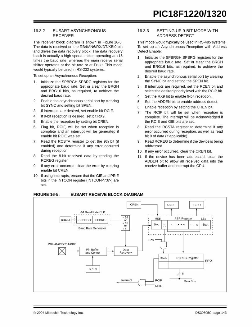
PIC18F1220/1320
16.3.2 EUSART ASYNCHRONOUS RECEIVER
The receiver block diagram is shown in Figure 16-5.The data is received on the RB4/AN6/RX/DT/KBI0 pinand drives the data recovery block. The data recoveryblock is actually a high-speed shifter, operating at x16times the baud rate, whereas the main receive serialshifter operates at the bit rate or at FOSC. This modewould typically be used in RS-232 systems.
To set up an Asynchronous Reception:
1. Initialize the SPBRGH:SPBRG registers for theappropriate baud rate. Set or clear the BRGHand BRG16 bits, as required, to achieve thedesired baud rate.
2. Enable the asynchronous serial port by clearingbit SYNC and setting bit SPEN.
3. If interrupts are desired, set enable bit RCIE.4. If 9-bit reception is desired, set bit RX9.5. Enable the reception by setting bit CREN.
6. Flag bit, RCIF, will be set when reception iscomplete and an interrupt will be generated ifenable bit RCIE was set.
7. Read the RCSTA register to get the 9th bit (ifenabled) and determine if any error occurredduring reception.
8. Read the 8-bit received data by reading theRCREG register.
9. If any error occurred, clear the error by clearingenable bit CREN.
10. If using interrupts, ensure that the GIE and PEIEbits in the INTCON register (INTCON<7:6>) areset.
16.3.3 SETTING UP 9-BIT MODE WITH ADDRESS DETECT
This mode would typically be used in RS-485 systems.To set up an Asynchronous Reception with AddressDetect Enable:
1. Initialize the SPBRGH:SPBRG registers for theappropriate baud rate. Set or clear the BRGHand BRG16 bits, as required, to achieve thedesired baud rate.
2. Enable the asynchronous serial port by clearingthe SYNC bit and setting the SPEN bit.
3. If interrupts are required, set the RCEN bit andselect the desired priority level with the RCIP bit.
4. Set the RX9 bit to enable 9-bit reception. 5. Set the ADDEN bit to enable address detect.
6. Enable reception by setting the CREN bit.7. The RCIF bit will be set when reception is
complete. The interrupt will be Acknowledged ifthe RCIE and GIE bits are set.
8. Read the RCSTA register to determine if anyerror occurred during reception, as well as readbit 9 of data (if applicable).
9. Read RCREG to determine if the device is beingaddressed.
10. If any error occurred, clear the CREN bit.
11. If the device has been addressed, clear theADDEN bit to allow all received data into thereceive buffer and interrupt the CPU.
FIGURE 16-5: EUSART RECEIVE BLOCK DIAGRAM
x64 Baud Rate CLK
Baud Rate Generator
RB4/AN6/RX/DT/KBI0
Pin Bufferand Control
SPEN
DataRecovery
CREN OERR FERR
RSR RegisterMSb LSb
RX9D RCREG RegisterFIFO
Interrupt RCIF
RCIE
Data Bus
8
÷ 64
÷ 16or
Stop Start(8) 7 1 0
RX9
• • •SPBRGSPBRGHBRG16
or÷ 4
2004 Microchip Technology Inc. DS39605C-page 143

PIC18F1220/1320
To set up an Asynchronous Transmission:
1. Initialize the SPBRG register for the appropriatebaud rate. If a high-speed baud rate is desired,set bit BRGH (see Section 16.2 “EUSARTBaud Rate Generator (BRG)”).
2. Enable the asynchronous serial port by clearingbit SYNC and setting bit SPEN.
3. If interrupts are desired, set enable bit TXIE.
4. If 9-bit transmission is desired, set transmit bitTX9. Can be used as address/data bit.
5. Enable the transmission by setting bit TXEN,which will also set bit TXIF.
6. If 9-bit transmission is selected, the ninth bitshould be loaded in bit TX9D.
7. Load data to the TXREG register (startstransmission).
If using interrupts, ensure that the GIE and PEIE bits inthe INTCON register (INTCON<7:6>) are set.
FIGURE 16-6: ASYNCHRONOUS RECEPTION
TABLE 16-6: REGISTERS ASSOCIATED WITH ASYNCHRONOUS RECEPTION
Startbit bit 7/8bit 1bit 0 bit 7/8 bit 0Stop
bit
Startbit
Startbitbit 7/8 Stop
bitRX (pin)
RegRcv Buffer Reg
Rcv Shift
Read RcvBuffer RegRCREG
RCIF(Interrupt Flag)
OERR bit
CREN
Word 1RCREG
Word 2RCREG
Stopbit
Note: This timing diagram shows three words appearing on the RX input. The RCREG (receive buffer) is read afterthe third word, causing the OERR (overrun) bit to be set.
Name Bit 7 Bit 6 Bit 5 Bit 4 Bit 3 Bit 2 Bit 1 Bit 0Value on
POR, BOR
Value onall otherResets
INTCON GIE/GIEH PEIE/GIEL TMR0IE INT0IE RBIE TMR0IF INT0IF RBIF 0000 000x 0000 000u
PIR1 — ADIF RCIF TXIF — CCP1IF TMR2IF TMR1IF -000 -000 -000 -000
PIE1 — ADIE RCIE TXIE — CCP1IE TMR2IE TMR1IE -000 -000 -000 -000
IPR1 — ADIP RCIP TXIP — CCP1IP TMR2IP TMR1IP -111 -111 -111 -111
RCSTA SPEN RX9 SREN CREN ADDEN FERR OERR RX9D 0000 000x 0000 000x
RCREG EUSART Receive Register 0000 0000 0000 0000
TXSTA CSRC TX9 TXEN SYNC SENDB BRGH TRMT TX9D 0000 0010 0000 0010
BAUDCTL — RCIDL — SCKP BRG16 — WUE ABDEN -1-1 0-00 -1-1 0-00
SPBRGH Baud Rate Generator Register High Byte 0000 0000 0000 0000
SPBRG Baud Rate Generator Register Low Byte 0000 0000 0000 0000
Legend: x = unknown, – = unimplemented locations read as ‘0’. Shaded cells are not used for asynchronous reception.
DS39605C-page 144 2004 Microchip Technology Inc.

PIC18F1220/1320
16.3.4 AUTO-WAKE-UP ON SYNC BREAK CHARACTER
During Sleep mode, all clocks to the EUSART aresuspended. Because of this, the Baud Rate Generatoris inactive and a proper byte reception cannot be per-formed. The auto-wake-up feature allows the controllerto wake-up due to activity on the RX/DT line while theEUSART is operating in Asynchronous mode.
The auto-wake-up feature is enabled by setting theWUE bit (BAUDCTL<1>). Once set, the typical receivesequence on RX/DT is disabled and the EUSARTremains in an Idle state, monitoring for a wake-up eventindependent of the CPU mode. A wake-up event con-sists of a high-to-low transition on the RX/DT line. (Thiscoincides with the start of a Sync Break or a Wake-upSignal character for the LIN protocol.)
Following a wake-up event, the module generates anRCIF interrupt. The interrupt is generated synchro-nously to the Q clocks in normal operating modes(Figure 16-7) and asynchronously if the device is inSleep mode (Figure 16-8). The interrupt condition iscleared by reading the RCREG register.
The WUE bit is automatically cleared once a low-to-hightransition is observed on the RX line, following the wake-up event. At this point, the EUSART module is in Idlemode and returns to normal operation. This signals tothe user that the Sync Break event is over.
16.3.4.1 Special Considerations Using Auto-Wake-up
Since auto-wake-up functions by sensing rising edgetransitions on RX/DT, information with any state changesbefore the Stop bit may signal a false end-of-character
and cause data or framing errors. To work properly,therefore, the initial character in the transmission mustbe all ‘0’s. This can be 00h (8 bytes) for standard RS-232devices, or 000h (12 bits) for LIN bus.
Oscillator start-up time must also be considered,especially in applications using oscillators with longerstart-up intervals (i.e., LP, XT or HS/PLL mode). TheSync Break (or Wake-up Signal) character must be ofsufficient length and be followed by a sufficient period,to allow enough time for the selected oscillator to startand provide proper initialization of the EUSART.
16.3.4.2 Special Considerations Using the WUE Bit
The timing of WUE and RCIF events may cause someconfusion when it comes to determining the validity ofreceived data. As noted, setting the WUE bit places theEUSART in an Idle mode. The wake-up event causesa receive interrupt by setting the RCIF bit. The WUE bitis cleared after this when a rising edge is seen on RX/DT. The interrupt condition is then cleared by readingthe RCREG register. Ordinarily, the data in RCREG willbe dummy data and should be discarded.
The fact that the WUE bit has been cleared (or is stillset) and the RCIF flag is set should not be used as anindicator of the integrity of the data in RCREG. Usersshould consider implementing a parallel method infirmware to verify received data integrity.
To assure that no actual data is lost, check the RCIDLbit to verify that a receive operation is not in process. Ifa receive operation is not occurring, the WUE bit maythen be set just prior to entering the Sleep mode.
FIGURE 16-7: AUTO-WAKE-UP BIT (WUE) TIMINGS DURING NORMAL OPERATION
FIGURE 16-8: AUTO-WAKE-UP BIT (WUE) TIMINGS DURING SLEEP
Q1 Q2 Q3 Q4 Q1 Q2 Q3 Q4 Q1 Q2 Q3 Q4 Q1 Q2 Q3 Q4 Q1 Q2 Q3 Q4 Q1 Q2 Q3 Q4 Q1 Q2 Q3 Q4 Q1 Q2 Q3 Q4 Q1 Q2 Q3 Q4 Q1 Q2 Q3 Q4
OSC1
WUE bit
RX/DT Line
RCIFCleared due to User Read of RCREG
Note 1: The EUSART remains in Idle while the WUE bit is set.
Bit Set by User Cleared by hardware
Q1 Q2 Q3 Q4 Q1 Q2 Q3 Q4 Q1 Q2 Q3 Q4 Q1 Q2 Q3 Q4 Q1 Q2 Q3 Q4 Q1 Q2 Q3 Q4 Q1 Q2 Q3 Q4 Q1 Q2 Q3 Q4
OSC1
WUE bit
RX/DT Line
RCIFCleared due to User Read of RCREG
Note 1: If the wake-up event requires a long oscillator warm-up time, the WUE bit may be cleared while the primary clock is still starting.
2: The EUSART remains in Idle while the WUE bit is set.
Sleep Ends
Enters SleepBit Set by User Cleared by hardware
Note 1
2004 Microchip Technology Inc. DS39605C-page 145
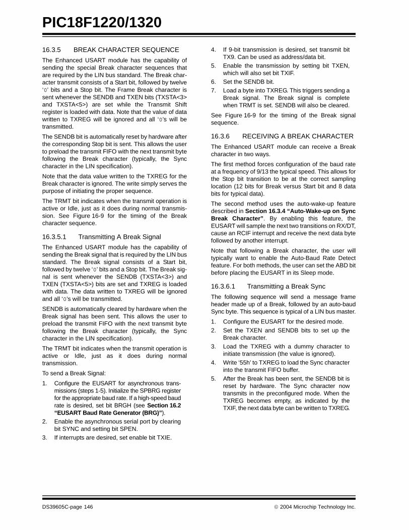
PIC18F1220/1320
16.3.5 BREAK CHARACTER SEQUENCE
The Enhanced USART module has the capability ofsending the special Break character sequences thatare required by the LIN bus standard. The Break char-acter transmit consists of a Start bit, followed by twelve‘0’ bits and a Stop bit. The Frame Break character issent whenever the SENDB and TXEN bits (TXSTA<3>and TXSTA<5>) are set while the Transmit Shiftregister is loaded with data. Note that the value of datawritten to TXREG will be ignored and all ‘0’s will betransmitted.
The SENDB bit is automatically reset by hardware afterthe corresponding Stop bit is sent. This allows the userto preload the transmit FIFO with the next transmit bytefollowing the Break character (typically, the Synccharacter in the LIN specification).
Note that the data value written to the TXREG for theBreak character is ignored. The write simply serves thepurpose of initiating the proper sequence.
The TRMT bit indicates when the transmit operation isactive or Idle, just as it does during normal transmis-sion. See Figure 16-9 for the timing of the Breakcharacter sequence.
16.3.5.1 Transmitting A Break Signal
The Enhanced USART module has the capability ofsending the Break signal that is required by the LIN busstandard. The Break signal consists of a Start bit,followed by twelve ‘0’ bits and a Stop bit. The Break sig-nal is sent whenever the SENDB (TXSTA<3>) andTXEN (TXSTA<5>) bits are set and TXREG is loadedwith data. The data written to TXREG will be ignoredand all ‘0’s will be transmitted.
SENDB is automatically cleared by hardware when theBreak signal has been sent. This allows the user topreload the transmit FIFO with the next transmit bytefollowing the Break character (typically, the Synccharacter in the LIN specification).
The TRMT bit indicates when the transmit operation isactive or Idle, just as it does during normaltransmission.
To send a Break Signal:
1. Configure the EUSART for asynchronous trans-missions (steps 1-5). Initialize the SPBRG registerfor the appropriate baud rate. If a high-speed baudrate is desired, set bit BRGH (see Section 16.2“EUSART Baud Rate Generator (BRG)”).
2. Enable the asynchronous serial port by clearingbit SYNC and setting bit SPEN.
3. If interrupts are desired, set enable bit TXIE.
4. If 9-bit transmission is desired, set transmit bitTX9. Can be used as address/data bit.
5. Enable the transmission by setting bit TXEN,which will also set bit TXIF.
6. Set the SENDB bit.7. Load a byte into TXREG. This triggers sending a
Break signal. The Break signal is completewhen TRMT is set. SENDB will also be cleared.
See Figure 16-9 for the timing of the Break signalsequence.
16.3.6 RECEIVING A BREAK CHARACTER
The Enhanced USART module can receive a Breakcharacter in two ways.
The first method forces configuration of the baud rateat a frequency of 9/13 the typical speed. This allows forthe Stop bit transition to be at the correct samplinglocation (12 bits for Break versus Start bit and 8 databits for typical data).
The second method uses the auto-wake-up featuredescribed in Section 16.3.4 “Auto-Wake-up on SyncBreak Character”. By enabling this feature, theEUSART will sample the next two transitions on RX/DT,cause an RCIF interrupt and receive the next data bytefollowed by another interrupt.
Note that following a Break character, the user willtypically want to enable the Auto-Baud Rate Detectfeature. For both methods, the user can set the ABD bitbefore placing the EUSART in its Sleep mode.
16.3.6.1 Transmitting a Break Sync
The following sequence will send a message frameheader made up of a Break, followed by an auto-baudSync byte. This sequence is typical of a LIN bus master.
1. Configure the EUSART for the desired mode.
2. Set the TXEN and SENDB bits to set up theBreak character.
3. Load the TXREG with a dummy character toinitiate transmission (the value is ignored).
4. Write ‘55h’ to TXREG to load the Sync characterinto the transmit FIFO buffer.
5. After the Break has been sent, the SENDB bit isreset by hardware. The Sync character nowtransmits in the preconfigured mode. When theTXREG becomes empty, as indicated by theTXIF, the next data byte can be written to TXREG.
DS39605C-page 146 2004 Microchip Technology Inc.

PIC18F1220/1320
16.3.6.2 Receiving a Break Sync
To receive a Break Sync:
1. Configure the EUSART for asynchronoustransmit and receive. TXEN should remainclear. SPBRGH:SPBRG may be left as is.
2. Enable auto-wake-up. Set WUE. 3. Enable RXIF interrupts. Set RCIE, PEIE, GIE.
4. The controller may be placed in any powermanaged mode.
5. An RCIF will be generated at the beginning ofthe Break signal. When the interrupt is received,read RCREG to clear RCIF and discard. Allowthe controller to return to PRI_RUN mode.
6. Wait for the RX line to go high at the end of theBreak signal. Wait for any of the following: WUEto clear automatically (poll), RB4/RX to go high(poll) or for RBIF to be set (poll or interrupt). IfRBIF is used, check to be sure that RB4/RX ishigh before continuing.
7. Enable Auto-Baud Rate Detect. Set ABDEN.8. Return from the interrupt. Allow the primary
clock to start and stabilize (PRI_RUN orPRI_IDLE).
9. When the next RCIF interrupt occurs, thereceived baud rate has been measured. ReadRCREG to clear RCIF and discard. CheckSPBRGH:SPBRG for a valid value. TheEUSART is ready for normal communications.Return from the interrupt. Allow the primaryclock to run (PRI_RUN or PRI_IDLE).
10. Process subsequent RCIF interrupts normallyas in asynchronous reception. TXEN shouldnow be set if transmissions are needed. TXIFand TXIE may be set if transmit interrupts aredesired. Remain in PRI_RUN or PRI_IDLE untilcommunications are complete. Clear TXEN andreturn to step 2.
FIGURE 16-9: SEND BREAK CHARACTER SEQUENCE
Write to TXREG
BRG Output(Shift Clock)
Start Bit Bit 0 Bit 1 Bit 11 Stop Bit
Break
TXIF bit
TX (pin)
TRMT bit
SENDB
Dummy Write
2004 Microchip Technology Inc. DS39605C-page 147

PIC18F1220/1320
16.4 EUSART Synchronous Master Mode
The Synchronous Master mode is entered by settingthe CSRC bit (TXSTA<7>). In this mode, the data istransmitted in a half-duplex manner (i.e., transmissionand reception do not occur at the same time). Whentransmitting data, the reception is inhibited and viceversa. Synchronous mode is entered by setting bit,SYNC (TXSTA<4>). In addition, enable bit, SPEN(RCSTA<7>), is set in order to configure the RB1/AN5/TX/CK/INT1 and RB4/AN6/RX/DT/KBI0 I/O pins to CK(clock) and DT (data) lines, respectively.
The Master mode indicates that the processor trans-mits the master clock on the CK line. Clock polarity isselected with the SCKP bit (BAUDCTL<5>); settingSCKP sets the Idle state on CK as high, while clearingthe bit sets the Idle state as low. This option is providedto support Microwire devices with this module.
16.4.1 EUSART SYNCHRONOUS MASTER TRANSMISSION
The EUSART transmitter block diagram is shown inFigure 16-2. The heart of the transmitter is the Transmit(Serial) Shift Register (TSR). The shift register obtainsits data from the Read/Write Transmit Buffer register,TXREG. The TXREG register is loaded with data insoftware. The TSR register is not loaded until the lastbit has been transmitted from the previous load. Assoon as the last bit is transmitted, the TSR is loadedwith new data from the TXREG (if available).
Once the TXREG register transfers the data to the TSRregister (occurs in one TCYCLE), the TXREG is emptyand interrupt bit, TXIF (PIR1<4>), is set. The interruptcan be enabled/disabled by setting/clearing enable bit,TXIE (PIE1<4>). Flag bit, TXIF, will be set, regardlessof the state of enable bit, TXIE and cannot be clearedin software. It will reset only when new data is loadedinto the TXREG register.
While flag bit, TXIF, indicates the status of the TXREGregister, another bit, TRMT (TXSTA<1>), shows thestatus of the TSR register. TRMT is a read-only bit,which is set when the TSR is empty. No interrupt logic istied to this bit, so the user has to poll this bit in order todetermine if the TSR register is empty. The TSR is notmapped in data memory, so it is not available to the user.
To set up a Synchronous Master Transmission:
1. Initialize the SPBRGH:SPBRG registers for theappropriate baud rate. Set or clear the BRGHand BRG16 bits, as required, to achieve thedesired baud rate.
2. Enable the synchronous master serial port bysetting bits SYNC, SPEN and CSRC.
3. If interrupts are desired, set enable bit TXIE.4. If 9-bit transmission is desired, set bit TX9.
5. Enable the transmission by setting bit TXEN.6. If 9-bit transmission is selected, the ninth bit
should be loaded in bit TX9D.7. Start transmission by loading data to the TXREG
register.8. If using interrupts, ensure that the GIE and PEIE
bits in the INTCON register (INTCON<7:6>) areset.
FIGURE 16-10: SYNCHRONOUS TRANSMISSION
bit 0 bit 1 bit 7
Word 1
Q1 Q2 Q3Q4 Q1 Q2 Q3 Q4 Q1 Q2 Q3 Q4 Q1Q2 Q3 Q4 Q1 Q2 Q3 Q4 Q3 Q4 Q1 Q2 Q3Q4 Q1Q2 Q3Q4 Q1 Q2Q3Q4 Q1 Q2Q3 Q4Q1 Q2 Q3 Q4 Q1 Q2 Q3 Q4
bit 2 bit 0 bit 1 bit 7RB4/AN6/RX/
RB1/AN5/TX/
Write toTXREG Reg
TXIF bit(Interrupt Flag)
TXEN bit‘1’ ‘1’
Word 2
TRMT bit
Write Word 1 Write Word 2
Note: Sync Master mode, SPBRG = 0, continuous transmission of two 8-bit words.
DT/KBI0 pin
CK/INT1 pin
RB1/AN5/TX/CK/INT1 pin
(SCKP = 0)
(SCKP = 1)
DS39605C-page 148 2004 Microchip Technology Inc.

PIC18F1220/1320
FIGURE 16-11: SYNCHRONOUS TRANSMISSION (THROUGH TXEN)
TABLE 16-7: REGISTERS ASSOCIATED WITH SYNCHRONOUS MASTER TRANSMISSION
RB4/AN6/RX/DT/KBI0 pin
RB1/AN5/TX/CK/INT1 pin
Write toTXREG reg
TXIF bit
TRMT bit
bit 0 bit 1 bit 2 bit 6 bit 7
TXEN bit
Name Bit 7 Bit 6 Bit 5 Bit 4 Bit 3 Bit 2 Bit 1 Bit 0Value on
POR, BOR
Value on all other Resets
INTCON GIE/GIEH PEIE/GIEL TMR0IE INT0IE RBIE TMR0IF INT0IF RBIF 0000 000x 0000 000u
PIR1 — ADIF RCIF TXIF — CCP1IF TMR2IF TMR1IF -000 -000 -000 -000
PIE1 — ADIE RCIE TXIE — CCP1IE TMR2IE TMR1IE -000 -000 -000 -000
IPR1 — ADIP RCIP TXIP — CCP1IP TMR2IP TMR1IP -111 -111 -111 -111
RCSTA SPEN RX9 SREN CREN ADDEN FERR OERR RX9D 0000 -00x 0000 -00x
TXREG EUSART Transmit Register 0000 0000 0000 0000
TXSTA CSRC TX9 TXEN SYNC SENDB BRGH TRMT TX9D 0000 0010 0000 0010
BAUDCTL — RCIDL — SCKP BRG16 — WUE ABDEN -1-1 0-00 -1-1 0-00
SPBRGH Baud Rate Generator Register High Byte 0000 0000 0000 0000
SPBRG Baud Rate Generator Register Low Byte 0000 0000 0000 0000
Legend: x = unknown, – = unimplemented, read as ‘0’. Shaded cells are not used for synchronous master transmission.
2004 Microchip Technology Inc. DS39605C-page 149

PIC18F1220/1320
16.4.2 EUSART SYNCHRONOUS MASTER RECEPTION
Once Synchronous mode is selected, reception isenabled by setting either the Single Receive Enable bit,SREN (RCSTA<5>), or the Continuous ReceiveEnable bit, CREN (RCSTA<4>). Data is sampled on theRB4/AN6/RX/DT/KBI0 pin on the falling edge of theclock.
If enable bit, SREN, is set, only a single word isreceived. If enable bit, CREN, is set, the reception iscontinuous until CREN is cleared. If both bits are set,then CREN takes precedence.
To set up a Synchronous Master Reception:
1. Initialize the SPBRGH:SPBRG registers for theappropriate baud rate. Set or clear the BRGHand BRG16 bits, as required, to achieve thedesired baud rate.
2. Enable the synchronous master serial port bysetting bits SYNC, SPEN and CSRC.
3. Ensure bits CREN and SREN are clear.4. If interrupts are desired, set enable bit RCIE.
5. If 9-bit reception is desired, set bit RX9.6. If a single reception is required, set bit SREN.
For continuous reception, set bit CREN.7. Interrupt flag bit, RCIF, will be set when reception
is complete and an interrupt will be generated ifthe enable bit, RCIE, was set.
8. Read the RCSTA register to get the 9th bit (ifenabled) and determine if any error occurredduring reception.
9. Read the 8-bit received data by reading theRCREG register.
10. If any error occurred, clear the error by clearingbit CREN.
11. If using interrupts, ensure that the GIE and PEIEbits in the INTCON register (INTCON<7:6>) areset.
FIGURE 16-12: SYNCHRONOUS RECEPTION (MASTER MODE, SREN)
CREN bit
RB4/AN6/RX/
RB1/AN5/TX/
Write tobit SREN
SREN bit
RCIF bit(Interrupt)
ReadRXREG
Q3 Q4 Q1 Q2 Q3 Q4 Q1 Q2 Q3 Q4Q2 Q1 Q2 Q3 Q4 Q1 Q2 Q3 Q4 Q1 Q2 Q3 Q4 Q1 Q2 Q3 Q4 Q1Q2 Q3 Q4 Q1 Q2 Q3 Q4 Q1 Q2 Q3 Q4
‘0’
bit 0 bit 1 bit 2 bit 3 bit 4 bit 5 bit 6 bit 7
‘0’
Q1 Q2 Q3 Q4
Note: Timing diagram demonstrates Sync Master mode with bit SREN = 1 and bit BRGH = 0.
RB1/AN5/TX/
CK/INT1 pin
CK/INT1 pin
DT/KBI0 pin
(SCKP = 0)
(SCKP = 1)
DS39605C-page 150 2004 Microchip Technology Inc.
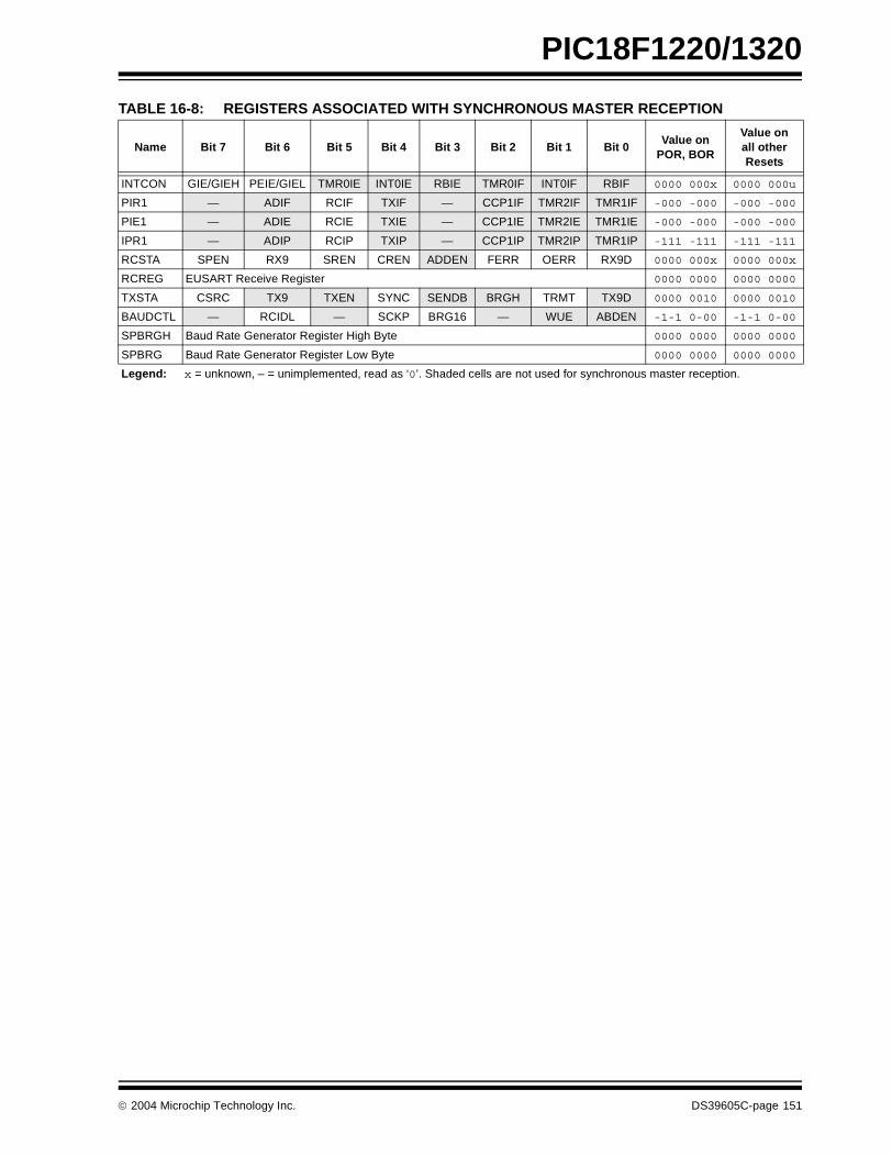
PIC18F1220/1320
TABLE 16-8: REGISTERS ASSOCIATED WITH SYNCHRONOUS MASTER RECEPTION
Name Bit 7 Bit 6 Bit 5 Bit 4 Bit 3 Bit 2 Bit 1 Bit 0Value on
POR, BOR
Value on all other Resets
INTCON GIE/GIEH PEIE/GIEL TMR0IE INT0IE RBIE TMR0IF INT0IF RBIF 0000 000x 0000 000u
PIR1 — ADIF RCIF TXIF — CCP1IF TMR2IF TMR1IF -000 -000 -000 -000
PIE1 — ADIE RCIE TXIE — CCP1IE TMR2IE TMR1IE -000 -000 -000 -000
IPR1 — ADIP RCIP TXIP — CCP1IP TMR2IP TMR1IP -111 -111 -111 -111
RCSTA SPEN RX9 SREN CREN ADDEN FERR OERR RX9D 0000 000x 0000 000x
RCREG EUSART Receive Register 0000 0000 0000 0000
TXSTA CSRC TX9 TXEN SYNC SENDB BRGH TRMT TX9D 0000 0010 0000 0010
BAUDCTL — RCIDL — SCKP BRG16 — WUE ABDEN -1-1 0-00 -1-1 0-00
SPBRGH Baud Rate Generator Register High Byte 0000 0000 0000 0000
SPBRG Baud Rate Generator Register Low Byte 0000 0000 0000 0000
Legend: x = unknown, – = unimplemented, read as ‘0’. Shaded cells are not used for synchronous master reception.
2004 Microchip Technology Inc. DS39605C-page 151
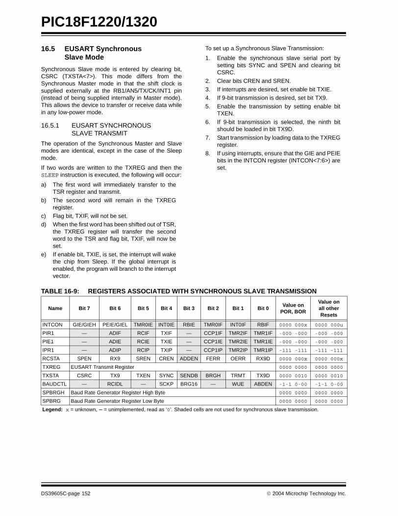
PIC18F1220/1320
16.5 EUSART Synchronous Slave Mode
Synchronous Slave mode is entered by clearing bit,CSRC (TXSTA<7>). This mode differs from theSynchronous Master mode in that the shift clock issupplied externally at the RB1/AN5/TX/CK/INT1 pin(instead of being supplied internally in Master mode).This allows the device to transfer or receive data whilein any low-power mode.
16.5.1 EUSART SYNCHRONOUS SLAVE TRANSMIT
The operation of the Synchronous Master and Slavemodes are identical, except in the case of the Sleepmode.
If two words are written to the TXREG and then theSLEEP instruction is executed, the following will occur:
a) The first word will immediately transfer to theTSR register and transmit.
b) The second word will remain in the TXREGregister.
c) Flag bit, TXIF, will not be set. d) When the first word has been shifted out of TSR,
the TXREG register will transfer the secondword to the TSR and flag bit, TXIF, will now beset.
e) If enable bit, TXIE, is set, the interrupt will wakethe chip from Sleep. If the global interrupt isenabled, the program will branch to the interruptvector.
To set up a Synchronous Slave Transmission:
1. Enable the synchronous slave serial port bysetting bits SYNC and SPEN and clearing bitCSRC.
2. Clear bits CREN and SREN.3. If interrupts are desired, set enable bit TXIE.4. If 9-bit transmission is desired, set bit TX9.
5. Enable the transmission by setting enable bitTXEN.
6. If 9-bit transmission is selected, the ninth bitshould be loaded in bit TX9D.
7. Start transmission by loading data to the TXREGregister.
8. If using interrupts, ensure that the GIE and PEIEbits in the INTCON register (INTCON<7:6>) areset.
TABLE 16-9: REGISTERS ASSOCIATED WITH SYNCHRONOUS SLAVE TRANSMISSION
Name Bit 7 Bit 6 Bit 5 Bit 4 Bit 3 Bit 2 Bit 1 Bit 0Value on
POR, BOR
Value on all other Resets
INTCON GIE/GIEH PEIE/GIEL TMR0IE INT0IE RBIE TMR0IF INT0IF RBIF 0000 000x 0000 000u
PIR1 — ADIF RCIF TXIF — CCP1IF TMR2IF TMR1IF -000 -000 -000 -000
PIE1 — ADIE RCIE TXIE — CCP1IE TMR2IE TMR1IE -000 -000 -000 -000
IPR1 — ADIP RCIP TXIP — CCP1IP TMR2IP TMR1IP -111 -111 -111 -111
RCSTA SPEN RX9 SREN CREN ADDEN FERR OERR RX9D 0000 000x 0000 000x
TXREG EUSART Transmit Register 0000 0000 0000 0000
TXSTA CSRC TX9 TXEN SYNC SENDB BRGH TRMT TX9D 0000 0010 0000 0010
BAUDCTL — RCIDL — SCKP BRG16 — WUE ABDEN -1-1 0-00 -1-1 0-00
SPBRGH Baud Rate Generator Register High Byte 0000 0000 0000 0000
SPBRG Baud Rate Generator Register Low Byte 0000 0000 0000 0000
Legend: x = unknown, – = unimplemented, read as ‘0’. Shaded cells are not used for synchronous slave transmission.
DS39605C-page 152 2004 Microchip Technology Inc.
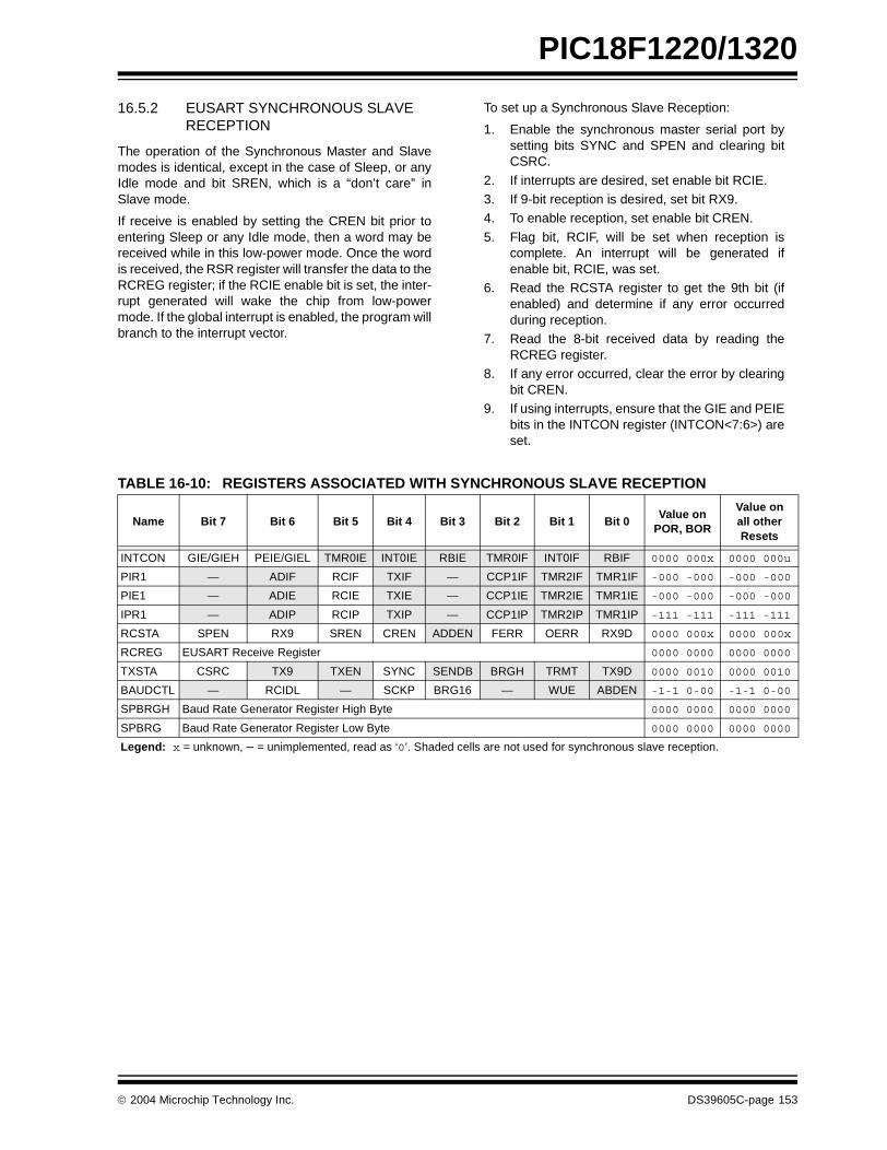
PIC18F1220/1320
16.5.2 EUSART SYNCHRONOUS SLAVE RECEPTION
The operation of the Synchronous Master and Slavemodes is identical, except in the case of Sleep, or anyIdle mode and bit SREN, which is a “don’t care” inSlave mode.
If receive is enabled by setting the CREN bit prior toentering Sleep or any Idle mode, then a word may bereceived while in this low-power mode. Once the wordis received, the RSR register will transfer the data to theRCREG register; if the RCIE enable bit is set, the inter-rupt generated will wake the chip from low-powermode. If the global interrupt is enabled, the program willbranch to the interrupt vector.
To set up a Synchronous Slave Reception:
1. Enable the synchronous master serial port bysetting bits SYNC and SPEN and clearing bitCSRC.
2. If interrupts are desired, set enable bit RCIE.3. If 9-bit reception is desired, set bit RX9.4. To enable reception, set enable bit CREN.
5. Flag bit, RCIF, will be set when reception iscomplete. An interrupt will be generated ifenable bit, RCIE, was set.
6. Read the RCSTA register to get the 9th bit (ifenabled) and determine if any error occurredduring reception.
7. Read the 8-bit received data by reading theRCREG register.
8. If any error occurred, clear the error by clearingbit CREN.
9. If using interrupts, ensure that the GIE and PEIEbits in the INTCON register (INTCON<7:6>) areset.
TABLE 16-10: REGISTERS ASSOCIATED WITH SYNCHRONOUS SLAVE RECEPTION
Name Bit 7 Bit 6 Bit 5 Bit 4 Bit 3 Bit 2 Bit 1 Bit 0Value on
POR, BOR
Value on all other Resets
INTCON GIE/GIEH PEIE/GIEL TMR0IE INT0IE RBIE TMR0IF INT0IF RBIF 0000 000x 0000 000u
PIR1 — ADIF RCIF TXIF — CCP1IF TMR2IF TMR1IF -000 -000 -000 -000
PIE1 — ADIE RCIE TXIE — CCP1IE TMR2IE TMR1IE -000 -000 -000 -000
IPR1 — ADIP RCIP TXIP — CCP1IP TMR2IP TMR1IP -111 -111 -111 -111
RCSTA SPEN RX9 SREN CREN ADDEN FERR OERR RX9D 0000 000x 0000 000x
RCREG EUSART Receive Register 0000 0000 0000 0000
TXSTA CSRC TX9 TXEN SYNC SENDB BRGH TRMT TX9D 0000 0010 0000 0010
BAUDCTL — RCIDL — SCKP BRG16 — WUE ABDEN -1-1 0-00 -1-1 0-00
SPBRGH Baud Rate Generator Register High Byte 0000 0000 0000 0000
SPBRG Baud Rate Generator Register Low Byte 0000 0000 0000 0000
Legend: x = unknown, – = unimplemented, read as ‘0’. Shaded cells are not used for synchronous slave reception.
2004 Microchip Technology Inc. DS39605C-page 153

PIC18F1220/1320
NOTES:
DS39605C-page 154 2004 Microchip Technology Inc.

PIC18F1220/1320
17.0 10-BIT ANALOG-TO-DIGITAL CONVERTER (A/D) MODULE
The Analog-to-Digital (A/D) converter module hasseven inputs for the PIC18F1220/1320 devices. Thismodule allows conversion of an analog input signal toa corresponding 10-bit digital number.
A new feature for the A/D converter is the addition ofprogrammable acquisition time. This feature allows theuser to select a new channel for conversion and to setthe GO/DONE bit immediately. When the GO/DONE bitis set, the selected channel is sampled for the pro-grammed acquisition time before a conversion is actu-ally started. This removes the firmware overhead thatmay have been required to allow for an acquisition(sampling) period (see Register 17-3 and Section 17.3“Selecting and Configuring Automatic AcquisitionTime”).
The module has five registers:
• A/D Result High Register (ADRESH)• A/D Result Low Register (ADRESL)
• A/D Control Register 0 (ADCON0)• A/D Control Register 1 (ADCON1)• A/D Control Register 2 (ADCON2)
The ADCON0 register, shown in Register 17-1,controls the operation of the A/D module. TheADCON1 register, shown in Register 17-2, configuresthe functions of the port pins. The ADCON2 register,shown in Register 17-3, configures the A/D clocksource, programmed acquisition time and justification.
REGISTER 17-1: ADCON0: A/D CONTROL REGISTER 0 R/W-0 R/W-0 U-0 R/W-0 R/W-0 R/W-0 R/W-0 R/W-0
VCFG1 VCFG0 — CHS2 CHS1 CHS0 GO/DONE ADON
bit 7 bit 0
bit 7-6 VCFG<1:0>: Voltage Reference Configuration bits
bit 5 Unimplemented: Read as ‘0’
bit 4-2 CHS2:CHS0: Analog Channel Select bits000 = Channel 0 (AN0) 001 = Channel 1 (AN1) 010 = Channel 2 (AN2) 011 = Channel 3 (AN3) 100 = Channel 4 (AN4) 101 = Channel 5 (AN5) 110 = Channel 6 (AN6)111 = Unimplemented(1)
bit 1 GO/DONE: A/D Conversion Status bitWhen ADON = 1: 1 = A/D conversion in progress0 = A/D Idle
bit 0 ADON: A/D On bit1 = A/D converter module is enabled 0 = A/D converter module is disabled
Note 1: Performing a conversion on unimplemented channels returns full-scale results.
Legend:
R = Readable bit W = Writable bit U = Unimplemented bit, read as ‘0’
-n = Value at POR ‘1’ = Bit is set ‘0’ = Bit is cleared x = Bit is unknown
A/D VREF+ A/D VREF-
00 AVDD AVSS
01 External VREF+ AVSS
10 AVDD External VREF-
11 External VREF+ External VREF-
2004 Microchip Technology Inc. DS39605C-page 155

PIC18F1220/1320
REGISTER 17-2: ADCON1: A/D CONTROL REGISTER 1 U-0 R/W-0 R/W-0 R/W-0 R/W-0 R/W-0 R/W-0 R/W-0
— PCFG6 PCFG5 PCFG4 PCFG3 PCFG2 PCFG1 PCFG0
bit 7 bit 0
bit 7 Unimplemented: Read as ‘0’
bit 6 PCFG6: A/D Port Configuration bit – AN61 = Pin configured as a digital port0 = Pin configured as an analog channel – digital input disabled and reads ‘0’
bit 5 PCFG5: A/D Port Configuration bit – AN51 = Pin configured as a digital port0 = Pin configured as an analog channel – digital input disabled and reads ‘0’
bit 4 PCFG4: A/D Port Configuration bit – AN41 = Pin configured as a digital port0 = Pin configured as an analog channel – digital input disabled and reads ‘0’
bit 3 PCFG3: A/D Port Configuration bit – AN31 = Pin configured as a digital port0 = Pin configured as an analog channel – digital input disabled and reads ‘0’
bit 2 PCFG2: A/D Port Configuration bit – AN21 = Pin configured as a digital port0 = Pin configured as an analog channel – digital input disabled and reads ‘0’
bit 1 PCFG1: A/D Port Configuration bit – AN11 = Pin configured as a digital port0 = Pin configured as an analog channel – digital input disabled and reads ‘0’
bit 0 PCFG0: A/D Port Configuration bit – AN01 = Pin configured as a digital port0 = Pin configured as an analog channel – digital input disabled and reads ‘0’
Legend:
R = Readable bit W = Writable bit U = Unimplemented bit, read as ‘0’
-n = Value at POR ‘1’ = Bit is set ‘0’ = Bit is cleared x = Bit is unknown
DS39605C-page 156 2004 Microchip Technology Inc.

PIC18F1220/1320
REGISTER 17-3: ADCON2: A/D CONTROL REGISTER 2 R/W-0 U-0 R/W-0 R/W-0 R/W-0 R/W-0 R/W-0 R/W-0
ADFM — ACQT2 ACQT1 ACQT0 ADCS2 ADCS1 ADCS0
bit 7 bit 0
bit 7 ADFM: A/D Result Format Select bit1 = Right justified 0 = Left justified
bit 6 Unimplemented: Read as ‘0’
bit 5-3 ACQT2:ACQT0: A/D Acquisition Time Select bits000 = 0 TAD(1)
001 = 2 TAD
010 = 4 TAD
011 = 6 TAD
100 = 8 TAD
101 = 12 TAD
110 = 16 TAD
111 = 20 TAD
bit 2-0 ADCS2:ADCS0: A/D Conversion Clock Select bits000 = FOSC/2001 = FOSC/8 010 = FOSC/32 011 = FRC (clock derived from A/D RC oscillator)(1) 100 = FOSC/4 101 = FOSC/16 110 = FOSC/64 111 = FRC (clock derived from A/D RC oscillator)(1)
Note: If the A/D FRC clock source is selected, a delay of one TCY (instruction cycle) isadded before the A/D clock starts. This allows the SLEEP instruction to be executedbefore starting a conversion.
Legend:
R = Readable bit W = Writable bit U = Unimplemented bit, read as ‘0’
-n = Value at POR ‘1’ = Bit is set ‘0’ = Bit is cleared x = Bit is unknown
2004 Microchip Technology Inc. DS39605C-page 157

PIC18F1220/1320
The analog reference voltage is software selectable toeither the device’s positive and negative supply voltage(AVDD and AVSS), or the voltage level on theRA3/AN3/VREF+ and RA2/AN2/VREF- pins.
The A/D converter has a unique feature of being ableto operate while the device is in Sleep mode. To oper-ate in Sleep, the A/D conversion clock must be derivedfrom the A/D’s internal RC oscillator.
The output of the sample and hold is the input into theconverter, which generates the result via successiveapproximation.
A device Reset forces all registers to their Reset state.This forces the A/D module to be turned off and anyconversion in progress is aborted.
Each port pin associated with the A/D converter can beconfigured as an analog input, or as a digital I/O. TheADRESH and ADRESL registers contain the result ofthe A/D conversion. When the A/D conversion is com-plete, the result is loaded into the ADRESH/ADRESLregisters, the GO/DONE bit (ADCON0 register) iscleared and A/D Interrupt Flag bit, ADIF, is set. The blockdiagram of the A/D module is shown in Figure 17-1.
FIGURE 17-1: A/D BLOCK DIAGRAM
(Input Voltage)
VAIN
VREFHReferenceVoltage
AVDD
VCFG1:VCFG0
CHS2:CHS0
AN6(1)
AN5
AN4
AN3/VREF+
AN2/VREF-
AN1
AN0
111
110
101
100
011
010
001
000
10-bitConverter
VREFL
AVSS
A/D
Note 1: I/O pins have diode protection to VDD and VSS.
0x1xx1x0
AVDD
DS39605C-page 158 2004 Microchip Technology Inc.
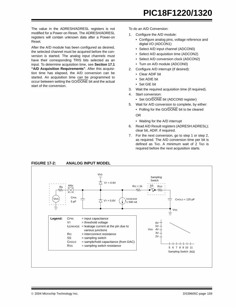
PIC18F1220/1320
The value in the ADRESH/ADRESL registers is notmodified for a Power-on Reset. The ADRESH/ADRESLregisters will contain unknown data after a Power-onReset.
After the A/D module has been configured as desired,the selected channel must be acquired before the con-version is started. The analog input channels musthave their corresponding TRIS bits selected as aninput. To determine acquisition time, see Section 17.1“A/D Acquisition Requirements”. After this acquisi-tion time has elapsed, the A/D conversion can bestarted. An acquisition time can be programmed tooccur between setting the GO/DONE bit and the actualstart of the conversion.
To do an A/D Conversion:
1. Configure the A/D module:• Configure analog pins, voltage reference and
digital I/O (ADCON1)• Select A/D input channel (ADCON0)
• Select A/D acquisition time (ADCON2)• Select A/D conversion clock (ADCON2)• Turn on A/D module (ADCON0)
2. Configure A/D interrupt (if desired):• Clear ADIF bit • Set ADIE bit
• Set GIE bit 3. Wait the required acquisition time (if required).4. Start conversion:
• Set GO/DONE bit (ADCON0 register)5. Wait for A/D conversion to complete, by either:
• Polling for the GO/DONE bit to be cleared
OR
• Waiting for the A/D interrupt
6. Read A/D Result registers (ADRESH:ADRESL);clear bit, ADIF, if required.
7. For the next conversion, go to step 1 or step 2,as required. The A/D conversion time per bit isdefined as TAD. A minimum wait of 2 TAD isrequired before the next acquisition starts.
FIGURE 17-2: ANALOG INPUT MODEL
VAIN CPIN
Rs ANx
5 pF
VDD
VT = 0.6V
VT = 0.6VILEAKAGE
RIC ≤ 1k
SamplingSwitch
SS RSS
CHOLD = 120 pF
VSS
6V
Sampling Switch
5V4V3V2V
5 6 7 8 9 10 11
(kΩ)
VDD
± 500 nA
Legend: CPIN = input capacitanceVT = threshold voltageILEAKAGE = leakage current at the pin due to
various junctionsRIC = interconnect resistanceSS = sampling switchCHOLD = sample/hold capacitance (from DAC)RSS = sampling switch resistance
2004 Microchip Technology Inc. DS39605C-page 159

PIC18F1220/1320
17.1 A/D Acquisition Requirements
For the A/D converter to meet its specified accuracy,the charge holding capacitor (CHOLD) must be allowedto fully charge to the input channel voltage level. Theanalog input model is shown in Figure 17-2. Thesource impedance (RS) and the internal samplingswitch (RSS) impedance directly affect the timerequired to charge the capacitor CHOLD. The samplingswitch (RSS) impedance varies over the device voltage(VDD). The source impedance affects the offset voltageat the analog input (due to pin leakage current). Themaximum recommended impedance for analogsources is 2.5 kΩ. After the analog input channel isselected (changed), the channel must be sampled forat least the minimum acquisition time before starting aconversion.
To calculate the minimum acquisition time,Equation 17-1 may be used. This equation assumesthat 1/2 LSb error is used (1024 steps for the A/D). The1/2 LSb error is the maximum error allowed for the A/Dto meet its specified resolution.
Example 17-1 shows the calculation of the minimumrequired acquisition time, TACQ. This calculation isbased on the following application systemassumptions:
CHOLD = 120 pF Rs = 2.5 kΩ Conversion Error ≤ 1/2 LSb VDD = 5V → RSS = 7 kΩ Temperature = 50°C (system max.) VHOLD = 0V @ time = 0
17.2 A/D VREF+ and VREF- References
If external voltage references are used instead of theinternal AVDD and AVSS sources, the source imped-ance of the VREF+ and VREF- voltage sources must beconsidered. During acquisition, currents supplied bythese sources are insignificant. However, duringconversion, the A/D module sinks and sources currentthrough the reference sources.
In order to maintain the A/D accuracy, the voltagereference source impedances should be kept low toreduce voltage changes. These voltage changes occuras reference currents flow through the referencesource impedance. The maximum recommendedimpedance of the VREF+ and VREF- externalreference voltage sources is 250Ω.
EQUATION 17-1: ACQUISITION TIME
EQUATION 17-2: A/D MINIMUM CHARGING TIME
EXAMPLE 17-1: CALCULATING THE MINIMUM REQUIRED ACQUISITION TIME
Note: When the conversion is started, theholding capacitor is disconnected from theinput pin.
TACQ = Amplifier Settling Time + Holding Capacitor Charging Time + Temperature Coefficient = TAMP + TC + TCOFF
VHOLD = (∆VREF – (∆VREF/2048)) • (1 – e(-TC/CHOLD(RIC + RSS + RS))) or TC = -(CHOLD)(RIC + RSS + RS) ln(1/2048)
TACQ = TAMP + TC + TCOFF
TAMP = 5 µs TCOFF = (Temp – 25ºC)(0.05 µs/ºC)
(50ºC – 25ºC)(0.05 µs/ºC)1.25 µs
Temperature coefficient is only required for temperatures > 25ºC. Below 25ºC, TCOFF = 0 µs.TC = -(CHOLD)(RIC + RSS + RS) ln(1/2047) µs
-(120 pF) (1 kΩ + 7 kΩ + 2.5 kΩ) ln(0.0004883) µs 9.61 µs
TACQ = 5 µs + 1.25 µs + 9.61 µs12.86 µs
DS39605C-page 160 2004 Microchip Technology Inc.
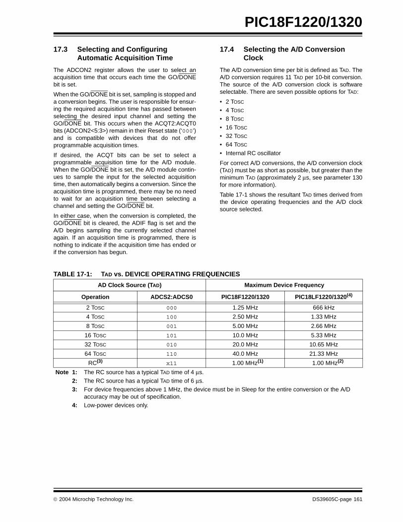
PIC18F1220/1320
17.3 Selecting and Configuring Automatic Acquisition Time
The ADCON2 register allows the user to select anacquisition time that occurs each time the GO/DONEbit is set.
When the GO/DONE bit is set, sampling is stopped anda conversion begins. The user is responsible for ensur-ing the required acquisition time has passed betweenselecting the desired input channel and setting theGO/DONE bit. This occurs when the ACQT2:ACQT0bits (ADCON2<5:3>) remain in their Reset state (‘000’)and is compatible with devices that do not offerprogrammable acquisition times.
If desired, the ACQT bits can be set to select aprogrammable acquisition time for the A/D module.When the GO/DONE bit is set, the A/D module contin-ues to sample the input for the selected acquisitiontime, then automatically begins a conversion. Since theacquisition time is programmed, there may be no needto wait for an acquisition time between selecting achannel and setting the GO/DONE bit.
In either case, when the conversion is completed, theGO/DONE bit is cleared, the ADIF flag is set and theA/D begins sampling the currently selected channelagain. If an acquisition time is programmed, there isnothing to indicate if the acquisition time has ended orif the conversion has begun.
17.4 Selecting the A/D Conversion Clock
The A/D conversion time per bit is defined as TAD. TheA/D conversion requires 11 TAD per 10-bit conversion.The source of the A/D conversion clock is softwareselectable. There are seven possible options for TAD:
• 2 TOSC
• 4 TOSC
• 8 TOSC
• 16 TOSC
• 32 TOSC • 64 TOSC
• Internal RC oscillator
For correct A/D conversions, the A/D conversion clock(TAD) must be as short as possible, but greater than theminimum TAD (approximately 2 µs, see parameter 130for more information).
Table 17-1 shows the resultant TAD times derived fromthe device operating frequencies and the A/D clocksource selected.
TABLE 17-1: TAD vs. DEVICE OPERATING FREQUENCIES
AD Clock Source (TAD) Maximum Device Frequency
Operation ADCS2:ADCS0 PIC18F1220/1320 PIC18LF1220/1320(4)
2 TOSC 000 1.25 MHz 666 kHz
4 TOSC 100 2.50 MHz 1.33 MHz
8 TOSC 001 5.00 MHz 2.66 MHz
16 TOSC 101 10.0 MHz 5.33 MHz
32 TOSC 010 20.0 MHz 10.65 MHz
64 TOSC 110 40.0 MHz 21.33 MHz
RC(3) x11 1.00 MHz(1) 1.00 MHz(2)
Note 1: The RC source has a typical TAD time of 4 µs.
2: The RC source has a typical TAD time of 6 µs.3: For device frequencies above 1 MHz, the device must be in Sleep for the entire conversion or the A/D
accuracy may be out of specification.4: Low-power devices only.
2004 Microchip Technology Inc. DS39605C-page 161

PIC18F1220/1320
17.5 Operation in Low-Power Modes
The selection of the automatic acquisition time and theA/D conversion clock is determined, in part, by the low-power mode clock source and frequency while in alow-power mode.
If the A/D is expected to operate while the device isin a low-power mode, the ACQT2:ACQT0 andADCS2:ADCS0 bits in ADCON2 should be updated inaccordance with the low-power mode clock that will beused. After the low-power mode is entered (either ofthe Run modes), an A/D acquisition or conversion maybe started. Once an acquisition or conversion isstarted, the device should continue to be clocked by thesame low-power mode clock source until the conver-sion has been completed. If desired, the device may beplaced into the corresponding low-power (ANY)_IDLEmode during the conversion.
If the low-power mode clock frequency is less than1 MHz, the A/D RC clock source should be selected.
Operation in the Low-Power Sleep mode requires theA/D RC clock to be selected. If bits, ACQT2:ACQT0, areset to ‘000’ and a conversion is started, the conversionwill be delayed one instruction cycle to allow executionof the SLEEP instruction and entry to Low-Power Sleepmode. The IDLEN and SCS bits in the OSCCON registermust have already been cleared prior to starting theconversion.
17.6 Configuring Analog Port Pins
The ADCON1, TRISA and TRISB registers all configurethe A/D port pins. The port pins needed as analog inputsmust have their corresponding TRIS bits set (input). Ifthe TRIS bit is cleared (output), the digital output level(VOH or VOL) will be converted.
The A/D operation is independent of the state of theCHS2:CHS0 bits and the TRIS bits.
Note 1: When reading the Port register, all pinsconfigured as analog input channels willread as cleared (a low level). Pins con-figured as digital inputs will convert ananalog input. Analog levels on a digitallyconfigured input will be accuratelyconverted.
2: Analog levels on any pin defined as adigital input may cause the digital inputbuffer to consume current out of thedevice’s specification limits.
DS39605C-page 162 2004 Microchip Technology Inc.
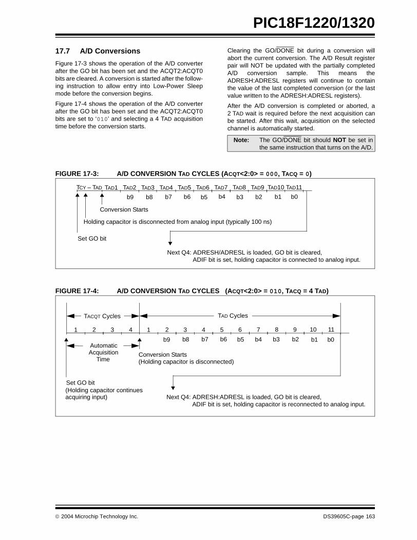
PIC18F1220/1320
17.7 A/D Conversions
Figure 17-3 shows the operation of the A/D converterafter the GO bit has been set and the ACQT2:ACQT0bits are cleared. A conversion is started after the follow-ing instruction to allow entry into Low-Power Sleepmode before the conversion begins.
Figure 17-4 shows the operation of the A/D converterafter the GO bit has been set and the ACQT2:ACQT0bits are set to ‘010’ and selecting a 4 TAD acquisitiontime before the conversion starts.
Clearing the GO/DONE bit during a conversion willabort the current conversion. The A/D Result registerpair will NOT be updated with the partially completedA/D conversion sample. This means theADRESH:ADRESL registers will continue to containthe value of the last completed conversion (or the lastvalue written to the ADRESH:ADRESL registers).
After the A/D conversion is completed or aborted, a2 TAD wait is required before the next acquisition canbe started. After this wait, acquisition on the selectedchannel is automatically started.
FIGURE 17-3: A/D CONVERSION TAD CYCLES (ACQT<2:0> = 000, TACQ = 0)
FIGURE 17-4: A/D CONVERSION TAD CYCLES (ACQT<2:0> = 010, TACQ = 4 TAD)
Note: The GO/DONE bit should NOT be set inthe same instruction that turns on the A/D.
TAD1 TAD2 TAD3 TAD4 TAD5 TAD6 TAD7 TAD8 TAD11
Set GO bit
Holding capacitor is disconnected from analog input (typically 100 ns)
TAD9 TAD10TCY – TAD
Next Q4: ADRESH/ADRESL is loaded, GO bit is cleared, ADIF bit is set, holding capacitor is connected to analog input.
Conversion Starts
b0b9 b6 b5 b4 b3 b2 b1b8 b7
1 2 3 4 5 6 7 8 11
Set GO bit
(Holding capacitor is disconnected)
9 10
Next Q4: ADRESH:ADRESL is loaded, GO bit is cleared, ADIF bit is set, holding capacitor is reconnected to analog input.
Conversion Starts
1 2 3 4
(Holding capacitor continuesacquiring input)
TACQT Cycles TAD Cycles
AutomaticAcquisition
Time
b0b9 b6 b5 b4 b3 b2 b1b8 b7
2004 Microchip Technology Inc. DS39605C-page 163

PIC18F1220/1320
17.8 Use of the CCP1 Trigger
An A/D conversion can be started by the “special eventtrigger” of the CCP1 module. This requires that theCCP1M3:CCP1M0 bits (CCP1CON<3:0>) be pro-grammed as ‘1011’ and that the A/D module is enabled(ADON bit is set). When the trigger occurs, theGO/DONE bit will be set, starting the A/D acquisitionand conversion and the Timer1 (or Timer3) counter willbe reset to zero. Timer1 (or Timer3) is reset to auto-matically repeat the A/D acquisition period with minimal
software overhead (moving ADRESH/ADRESL to thedesired location). The appropriate analog inputchannel must be selected and the minimum acquisitionperiod is either timed by the user, or an appropriateTACQ time selected before the “special event trigger”sets the GO/DONE bit (starts a conversion).
If the A/D module is not enabled (ADON is cleared), the“special event trigger” will be ignored by the A/Dmodule, but will still reset the Timer1 (or Timer3)counter.
TABLE 17-2: SUMMARY OF A/D REGISTERS
Name Bit 7 Bit 6 Bit 5 Bit 4 Bit 3 Bit 2 Bit 1 Bit 0Value on
POR, BOR
Value on all other Resets
INTCON GIE/GIEH
PEIE/GIEL
TMR0IE INT0IE RBIE TMR0IF INT0IF RBIF 0000 0000 0000 0000
PIR1 — ADIF RCIF TXIF — CCP1IF TMR2IF TMR1IF -000 -000 -000 -000
PIE1 — ADIE RCIE TXIE — CCP1IE TMR2IE TMR1IE -000 -000 -000 -000
IPR1 — ADIP RCIP TXIP — CCP1IP TMR2IP TMR1IP -111 -111 -111 -111
PIR2 OSCFIF — — EEIF — LVDIF TMR3IF — 0--0 -00- 0--0 -00-
PIE2 OSCFIE — — EEIE — LVDIE TMR3IE — 0--0 -00- 0--0 -00-
IPR2 OSCFIP — — EEIP — LVDIP TMR3IP — 1--1 -11- 1--1 -11-
ADRESH A/D Result Register High Byte xxxx xxxx uuuu uuuu
ADRESL A/D Result Register Low Byte xxxx xxxx uuuu uuuu
ADCON0 VCFG1 VCFG0 — CHS2 CHS1 CHS0 GO/DONE ADON 00-0 0000 00-0 0000
ADCON1 — PCFG6 PCFG5 PCFG4 PCFG3 PCFG2 PCFG1 PCFG0 -000 0000 -000 0000
ADCON2 ADFM — ACQT2 ACQT1 ACQT0 ADCS2 ADCS1 ADCS0 0-00 0000 0-00 0000
PORTA RA7(3) RA6(2) RA5(1) RA4 RA3 RA2 RA1 RA0 qq0x 0000 uu0u 0000
TRISA TRISA7(3) TRISA6(2) — PORTA Data Direction Register qq-1 1111 11-1 1111
PORTB Read PORTB pins, Write LATB Latch xxxx xxxx uuuu uuuu
TRISB PORTB Data Direction Register 1111 1111 1111 1111
LATB PORTB Output Data Latch xxxx xxxx uuuu uuuu
Legend: x = unknown, u = unchanged, q = depends on CONFIG1H<3:0>, – = unimplemented, read as ‘0’. Shaded cells are not used for A/D conversion.
Note 1: RA5 port bit is available only as an input pin when the MCLRE bit in the configuration register is ‘0’.2: RA6 and TRISA6 are available only when the primary oscillator mode selection offers RA6 as a port pin; otherwise, RA6
always reads ‘0’, TRISA6 always reads ‘1’ and writes to both are ignored (see CONFIG1H<3:0>).3: RA7 and TRISA7 are available only when the internal RC oscillator is configured as the primary oscillator in
CONFIG1H<3:0>; otherwise, RA7 always reads ‘0’, TRISA7 always reads ‘1’ and writes to both are ignored.
DS39605C-page 164 2004 Microchip Technology Inc.

PIC18F1220/1320
18.0 LOW-VOLTAGE DETECT
In many applications, the ability to determine if thedevice voltage (VDD) is below a specified voltage levelis a desirable feature. A window of operation for theapplication can be created, where the application soft-ware can do “housekeeping tasks”, before the devicevoltage exits the valid operating range. This can bedone using the Low-Voltage Detect module.
This module is a software programmable circuitry,where a device voltage trip point can be specified.When the voltage of the device becomes lower then thespecified point, an interrupt flag is set. If the interrupt isenabled, the program execution will branch to the inter-rupt vector address and the software can then respondto that interrupt source.
The Low-Voltage Detect circuitry is completely undersoftware control. This allows the circuitry to be turnedoff by the software, which minimizes the currentconsumption for the device.
Figure 18-1 shows a possible application voltage curve(typically for batteries). Over time, the device voltagedecreases. When the device voltage equals voltage VA,the LVD logic generates an interrupt. This occurs attime TA. The application software then has the time,until the device voltage is no longer in valid operatingrange, to shut down the system. Voltage point VB is theminimum valid operating voltage specification. Thisoccurs at time TB. The difference, TB – TA, is the totaltime for shutdown.
The block diagram for the LVD module is shown inFigure 18-2 (following page). A comparator uses aninternally generated reference voltage as the set point.When the selected tap output of the device voltagecrosses the set point (is lower than), the LVDIF bit is set.
Each node in the resistor divider represents a “trippoint” voltage. The “trip point” voltage is the minimumsupply voltage level at which the device can operatebefore the LVD module asserts an interrupt. When thesupply voltage is equal to the trip point, the voltagetapped off of the resistor array is equal to the 1.2Vinternal reference voltage generated by the voltagereference module. The comparator then generates aninterrupt signal setting the LVDIF bit. This voltage issoftware programmable to any one of 16 values (seeFigure 18-2). The trip point is selected byprogramming the LVDL3:LVDL0 bits (LVDCON<3:0>).
FIGURE 18-1: TYPICAL LOW-VOLTAGE DETECT APPLICATION
Time
Vo
ltag
e
VAVB
TA TB
Legend: VA = LVD trip pointVB = Minimum valid deviceoperating voltage
2004 Microchip Technology Inc. DS39605C-page 165
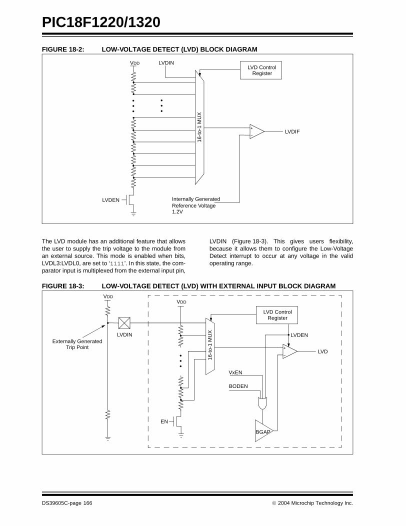
PIC18F1220/1320
FIGURE 18-2: LOW-VOLTAGE DETECT (LVD) BLOCK DIAGRAM
The LVD module has an additional feature that allowsthe user to supply the trip voltage to the module froman external source. This mode is enabled when bits,LVDL3:LVDL0, are set to ‘1111’. In this state, the com-parator input is multiplexed from the external input pin,
LVDIN (Figure 18-3). This gives users flexibility,because it allows them to configure the Low-VoltageDetect interrupt to occur at any voltage in the validoperating range.
FIGURE 18-3: LOW-VOLTAGE DETECT (LVD) WITH EXTERNAL INPUT BLOCK DIAGRAM
LVDIF
VDD
16-t
o-1
MU
XLVDEN
LVD ControlRegister
Internally GeneratedReference Voltage
LVDIN
1.2V
LVD
EN
LVD Control
16-t
o-1
MU
X
BGAP
BODEN
LVDEN
VxEN
LVDIN
Register
VDDVDD
Externally GeneratedTrip Point
DS39605C-page 166 2004 Microchip Technology Inc.
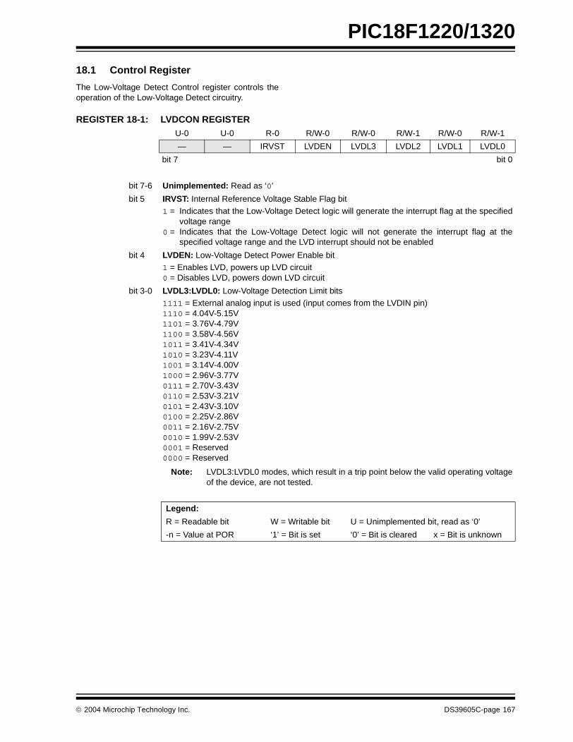
PIC18F1220/1320
18.1 Control Register
The Low-Voltage Detect Control register controls theoperation of the Low-Voltage Detect circuitry.
REGISTER 18-1: LVDCON REGISTER U-0 U-0 R-0 R/W-0 R/W-0 R/W-1 R/W-0 R/W-1
— — IRVST LVDEN LVDL3 LVDL2 LVDL1 LVDL0
bit 7 bit 0
bit 7-6 Unimplemented: Read as ‘0’
bit 5 IRVST: Internal Reference Voltage Stable Flag bit1 = Indicates that the Low-Voltage Detect logic will generate the interrupt flag at the specified
voltage range0 = Indicates that the Low-Voltage Detect logic will not generate the interrupt flag at the
specified voltage range and the LVD interrupt should not be enabled
bit 4 LVDEN: Low-Voltage Detect Power Enable bit1 = Enables LVD, powers up LVD circuit 0 = Disables LVD, powers down LVD circuit
bit 3-0 LVDL3:LVDL0: Low-Voltage Detection Limit bits1111 = External analog input is used (input comes from the LVDIN pin) 1110 = 4.04V-5.15V 1101 = 3.76V-4.79V 1100 = 3.58V-4.56V 1011 = 3.41V-4.34V 1010 = 3.23V-4.11V 1001 = 3.14V-4.00V 1000 = 2.96V-3.77V 0111 = 2.70V-3.43V 0110 = 2.53V-3.21V 0101 = 2.43V-3.10V 0100 = 2.25V-2.86V 0011 = 2.16V-2.75V 0010 = 1.99V-2.53V 0001 = Reserved 0000 = Reserved
Note: LVDL3:LVDL0 modes, which result in a trip point below the valid operating voltageof the device, are not tested.
Legend:
R = Readable bit W = Writable bit U = Unimplemented bit, read as ‘0’
-n = Value at POR ‘1’ = Bit is set ‘0’ = Bit is cleared x = Bit is unknown
2004 Microchip Technology Inc. DS39605C-page 167
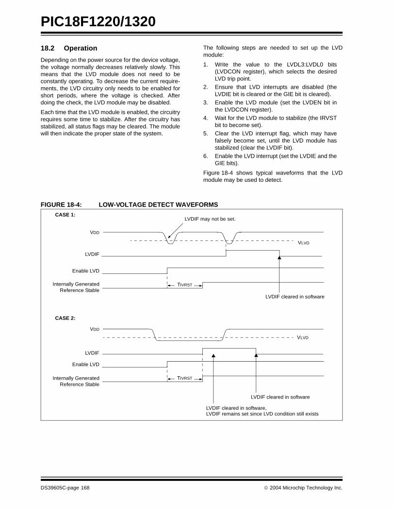
PIC18F1220/1320
18.2 Operation
Depending on the power source for the device voltage,the voltage normally decreases relatively slowly. Thismeans that the LVD module does not need to beconstantly operating. To decrease the current require-ments, the LVD circuitry only needs to be enabled forshort periods, where the voltage is checked. Afterdoing the check, the LVD module may be disabled.
Each time that the LVD module is enabled, the circuitryrequires some time to stabilize. After the circuitry hasstabilized, all status flags may be cleared. The modulewill then indicate the proper state of the system.
The following steps are needed to set up the LVDmodule:
1. Write the value to the LVDL3:LVDL0 bits(LVDCON register), which selects the desiredLVD trip point.
2. Ensure that LVD interrupts are disabled (theLVDIE bit is cleared or the GIE bit is cleared).
3. Enable the LVD module (set the LVDEN bit inthe LVDCON register).
4. Wait for the LVD module to stabilize (the IRVSTbit to become set).
5. Clear the LVD interrupt flag, which may havefalsely become set, until the LVD module hasstabilized (clear the LVDIF bit).
6. Enable the LVD interrupt (set the LVDIE and theGIE bits).
Figure 18-4 shows typical waveforms that the LVDmodule may be used to detect.
FIGURE 18-4: LOW-VOLTAGE DETECT WAVEFORMS
VLVD
VDD
LVDIF
VLVD
VDD
Enable LVD
Internally Generated TIVRST
LVDIF may not be set.
Enable LVD
LVDIF
LVDIF cleared in software
LVDIF cleared in software
LVDIF cleared in software,
CASE 1:
CASE 2:
LVDIF remains set since LVD condition still exists
Reference Stable
Internally GeneratedReference Stable
TIVRST
DS39605C-page 168 2004 Microchip Technology Inc.
PIC18F1220/1320
18.2.1 REFERENCE VOLTAGE SET POINT
The internal reference voltage of the LVD module maybe used by other internal circuitry (the programmableBrown-out Reset). If these circuits are disabled (lowercurrent consumption), the reference voltage circuitrequires a time to become stable before a low-voltagecondition can be reliably detected. This time is invariantof system clock speed. This start-up time is specified inelectrical specification parameter 36. The low-voltageinterrupt flag will not be enabled until a stable referencevoltage is reached. Refer to the waveform in Figure 18-4.
18.2.2 CURRENT CONSUMPTION
When the module is enabled, the LVD comparator andvoltage divider are enabled and will consume static cur-rent. The voltage divider can be tapped from multipleplaces in the resistor array. Total current consumption,when enabled, is specified in electrical specificationparameter D022B.
18.3 Operation During Sleep
When enabled, the LVD circuitry continues to operateduring Sleep. If the device voltage crosses the trippoint, the LVDIF bit will be set and the device will wake-up from Sleep. Device execution will continue from theinterrupt vector address if interrupts have been globallyenabled.
18.4 Effects of a Reset
A device Reset forces all registers to their Reset state.This forces the LVD module to be turned off.
2004 Microchip Technology Inc. DS39605C-page 169

PIC18F1220/1320
NOTES:
DS39605C-page 170 2004 Microchip Technology Inc.
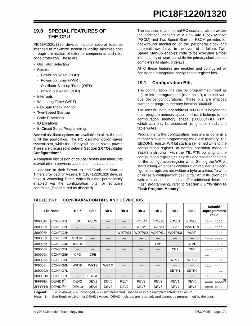
PIC18F1220/1320
19.0 SPECIAL FEATURES OF THE CPU
PIC18F1220/1320 devices include several featuresintended to maximize system reliability, minimize costthrough elimination of external components and offercode protection. These are:
• Oscillator Selection
• Resets:- Power-on Reset (POR)- Power-up Timer (PWRT)
- Oscillator Start-up Timer (OST)- Brown-out Reset (BOR)
• Interrupts
• Watchdog Timer (WDT)• Fail-Safe Clock Monitor• Two-Speed Start-up
• Code Protection• ID Locations• In-Circuit Serial Programming
Several oscillator options are available to allow the partto fit the application. The RC oscillator option savessystem cost, while the LP crystal option saves power.These are discussed in detail in Section 2.0 “OscillatorConfigurations”.
A complete discussion of device Resets and interruptsis available in previous sections of this data sheet.
In addition to their Power-up and Oscillator Start-upTimers provided for Resets, PIC18F1220/1320 deviceshave a Watchdog Timer, which is either permanentlyenabled via the configuration bits, or softwarecontrolled (if configured as disabled).
The inclusion of an internal RC oscillator also providesthe additional benefits of a Fail-Safe Clock Monitor(FSCM) and Two-Speed Start-up. FSCM provides forbackground monitoring of the peripheral clock andautomatic switchover in the event of its failure. Two-Speed Start-up enables code to be executed almostimmediately on start-up, while the primary clock sourcecompletes its start-up delays.
All of these features are enabled and configured bysetting the appropriate configuration register bits.
19.1 Configuration Bits
The configuration bits can be programmed (read as‘0’), or left unprogrammed (read as ‘1’), to select vari-ous device configurations. These bits are mappedstarting at program memory location 300000h.
The user will note that address 300000h is beyond theuser program memory space. In fact, it belongs to theconfiguration memory space (300000h-3FFFFFh),which can only be accessed using table reads andtable writes.
Programming the configuration registers is done in amanner similar to programming the Flash memory. TheEECON1 register WR bit starts a self-timed write to theconfiguration register. In normal operation mode, aTBLWT instruction, with the TBLPTR pointing to theconfiguration register, sets up the address and the datafor the configuration register write. Setting the WR bitstarts a long write to the configuration register. The con-figuration registers are written a byte at a time. To writeor erase a configuration cell, a TBLWT instruction canwrite a ‘1’ or a ‘0’ into the cell. For additional details onFlash programming, refer to Section 6.5 “Writing toFlash Program Memory”.
TABLE 19-1: CONFIGURATION BITS AND DEVICE IDS
File Name Bit 7 Bit 6 Bit 5 Bit 4 Bit 3 Bit 2 Bit 1 Bit 0Default/
UnprogrammedValue
300001h CONFIG1H IESO FSCM — — FOSC3 FOSC2 FOSC1 FOSC0 11-- 1111
300002h CONFIG2L — — — — BORV1 BORV0 BOR PWRTEN ---- 1111
300003h CONFIG2H — — — WDTPS3 WDTPS2 WDTPS1 WDTPS0 WDT ---1 1111
300005h CONFIG3H MCLRE — — — — — — — 1--- ----
300006h CONFIG4L DEBUG — — — — LVP — STVR 1--- -1-1
300008h CONFIG5L — — — — — — CP1 CP0 ---- --11
300009h CONFIG5H CPD CPB — — — — — — 11-- ----
30000Ah CONFIG6L — — — — — — WRT1 WRT0 ---- --11
30000Bh CONFIG6H WRTD WRTB WRTC — — — — — 111- ----
30000Ch CONFIG7L — — — — — — EBTR1 EBTR0 ---- --11
30000Dh CONFIG7H — EBTRB — — — — — — -1-- ----
3FFFFEh DEVID1(1) DEV2 DEV1 DEV0 REV4 REV3 REV2 REV1 REV0 xxxx xxxx(1)
3FFFFFh DEVID2(1) DEV10 DEV9 DEV8 DEV7 DEV6 DEV5 DEV4 DEV3 0000 0111
Legend: x = unknown, u = unchanged, – = unimplemented. Shaded cells are unimplemented, read as ‘0’.Note 1: See Register 19-14 for DEVID1 values. DEVID registers are read-only and cannot be programmed by the user.
2004 Microchip Technology Inc. DS39605C-page 171
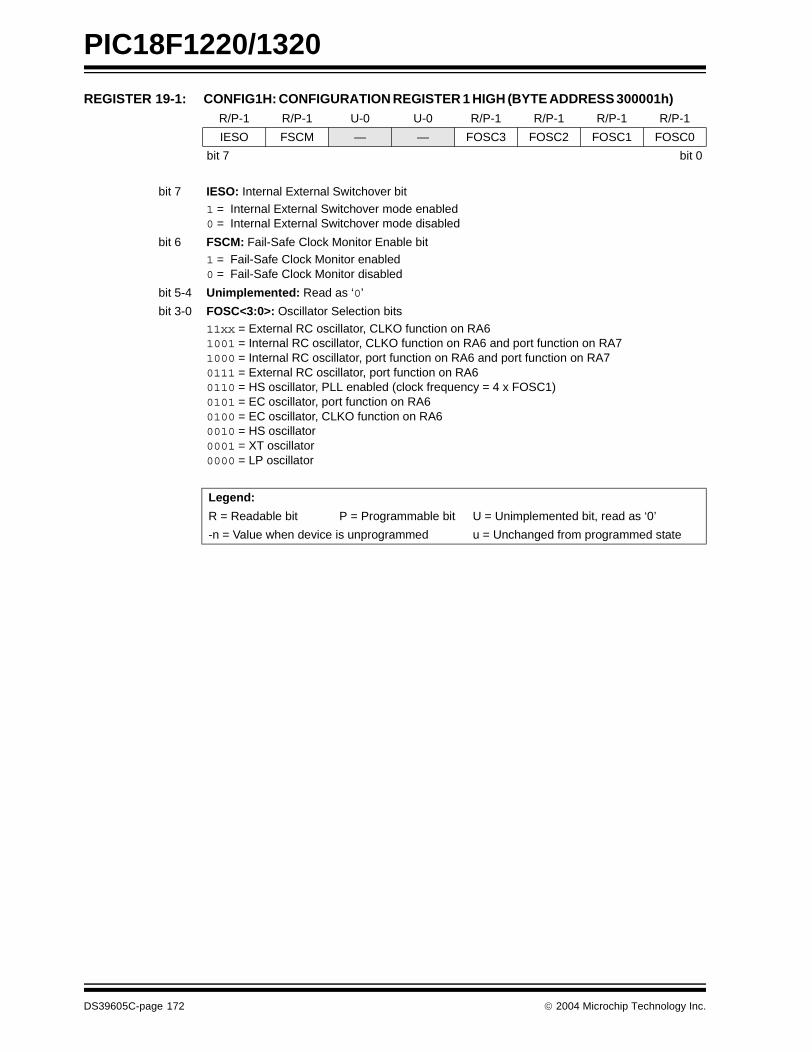
PIC18F1220/1320
REGISTER 19-1: CONFIG1H: CONFIGURATION REGISTER 1 HIGH (BYTE ADDRESS 300001h) R/P-1 R/P-1 U-0 U-0 R/P-1 R/P-1 R/P-1 R/P-1
IESO FSCM — — FOSC3 FOSC2 FOSC1 FOSC0
bit 7 bit 0
bit 7 IESO: Internal External Switchover bit
1 = Internal External Switchover mode enabled0 = Internal External Switchover mode disabled
bit 6 FSCM: Fail-Safe Clock Monitor Enable bit1 = Fail-Safe Clock Monitor enabled0 = Fail-Safe Clock Monitor disabled
bit 5-4 Unimplemented: Read as ‘0’
bit 3-0 FOSC<3:0>: Oscillator Selection bits
11xx = External RC oscillator, CLKO function on RA61001 = Internal RC oscillator, CLKO function on RA6 and port function on RA71000 = Internal RC oscillator, port function on RA6 and port function on RA70111 = External RC oscillator, port function on RA60110 = HS oscillator, PLL enabled (clock frequency = 4 x FOSC1)0101 = EC oscillator, port function on RA60100 = EC oscillator, CLKO function on RA60010 = HS oscillator0001 = XT oscillator0000 = LP oscillator
Legend:
R = Readable bit P = Programmable bit U = Unimplemented bit, read as ‘0’
-n = Value when device is unprogrammed u = Unchanged from programmed state
DS39605C-page 172 2004 Microchip Technology Inc.
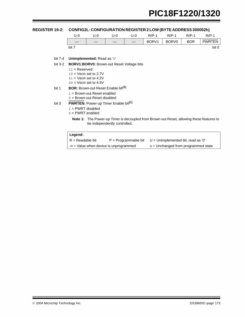
PIC18F1220/1320
REGISTER 19-2: CONFIG2L: CONFIGURATION REGISTER 2 LOW (BYTE ADDRESS 300002h) U-0 U-0 U-0 U-0 R/P-1 R/P-1 R/P-1 R/P-1
— — — — BORV1 BORV0 BOR PWRTEN
bit 7 bit 0
bit 7-4 Unimplemented: Read as ‘0’
bit 3-2 BORV1:BORV0: Brown-out Reset Voltage bits11 = Reserved 10 = VBOR set to 2.7V 01 = VBOR set to 4.2V 00 = VBOR set to 4.5V
bit 1 BOR: Brown-out Reset Enable bit(1)
1 = Brown-out Reset enabled 0 = Brown-out Reset disabled
bit 0 PWRTEN: Power-up Timer Enable bit(1)
1 = PWRT disabled 0 = PWRT enabled
Note 1: The Power-up Timer is decoupled from Brown-out Reset, allowing these features tobe independently controlled.
Legend:
R = Readable bit P = Programmable bit U = Unimplemented bit, read as ‘0’
-n = Value when device is unprogrammed u = Unchanged from programmed state
2004 Microchip Technology Inc. DS39605C-page 173

PIC18F1220/1320
REGISTER 19-3: CONFIG2H: CONFIGURATION REGISTER 2 HIGH (BYTE ADDRESS 300003h) U-0 U-0 U-0 R/P-1 R/P-1 R/P-1 R/P-1 R/P-1
— — — WDTPS3 WDTPS2 WDTPS1 WDTPS0 WDTEN
bit 7 bit 0
bit 7-5 Unimplemented: Read as ‘0’
bit 4-1 WDTPS<3:0>: Watchdog Timer Postscale Select bits
1111 = 1:32,7681110 = 1:16,3841101 = 1:8,1921100 = 1:4,0961011 = 1:2,0481010 = 1:1,0241001 = 1:5121000 = 1:2560111 = 1:1280110 = 1:640101 = 1:320100 = 1:160011 = 1:80010 = 1:40001 = 1:20000 = 1:1
bit 0 WDT: Watchdog Timer Enable bit
1 = WDT enabled0 = WDT disabled (control is placed on the SWDTEN bit)
Legend:R = Readable bit P = Programmable bit U = Unimplemented bit, read as ‘0’-n = Value when device is unprogrammed u = Unchanged from programmed state
DS39605C-page 174 2004 Microchip Technology Inc.
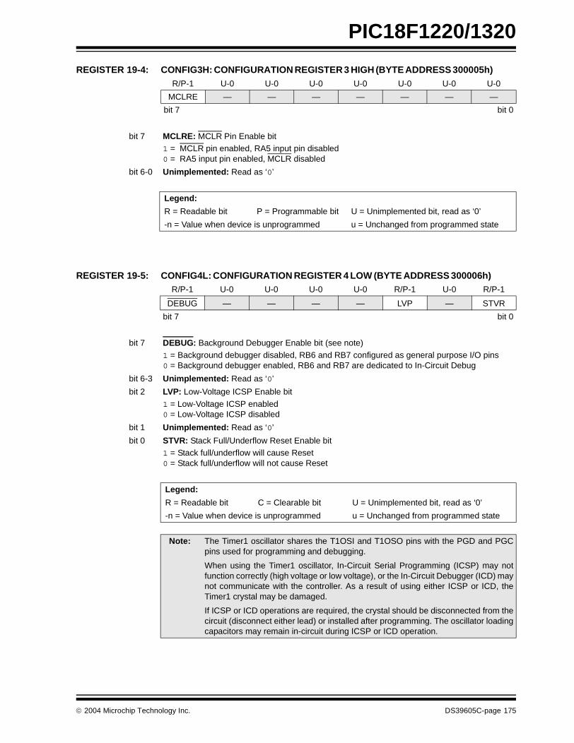
PIC18F1220/1320
REGISTER 19-4: CONFIG3H: CONFIGURATION REGISTER 3 HIGH (BYTE ADDRESS 300005h)
REGISTER 19-5: CONFIG4L: CONFIGURATION REGISTER 4 LOW (BYTE ADDRESS 300006h)
R/P-1 U-0 U-0 U-0 U-0 U-0 U-0 U-0
MCLRE — — — — — — —
bit 7 bit 0
bit 7 MCLRE: MCLR Pin Enable bit 1 = MCLR pin enabled, RA5 input pin disabled0 = RA5 input pin enabled, MCLR disabled
bit 6-0 Unimplemented: Read as ‘0’
Legend:
R = Readable bit P = Programmable bit U = Unimplemented bit, read as ‘0’
-n = Value when device is unprogrammed u = Unchanged from programmed state
R/P-1 U-0 U-0 U-0 U-0 R/P-1 U-0 R/P-1
DEBUG — — — — LVP — STVR
bit 7 bit 0
bit 7 DEBUG: Background Debugger Enable bit (see note)1 = Background debugger disabled, RB6 and RB7 configured as general purpose I/O pins 0 = Background debugger enabled, RB6 and RB7 are dedicated to In-Circuit Debug
bit 6-3 Unimplemented: Read as ‘0’
bit 2 LVP: Low-Voltage ICSP Enable bit
1 = Low-Voltage ICSP enabled 0 = Low-Voltage ICSP disabled
bit 1 Unimplemented: Read as ‘0’
bit 0 STVR: Stack Full/Underflow Reset Enable bit1 = Stack full/underflow will cause Reset 0 = Stack full/underflow will not cause Reset
Legend:
R = Readable bit C = Clearable bit U = Unimplemented bit, read as ‘0’
-n = Value when device is unprogrammed u = Unchanged from programmed state
Note: The Timer1 oscillator shares the T1OSI and T1OSO pins with the PGD and PGCpins used for programming and debugging.
When using the Timer1 oscillator, In-Circuit Serial Programming (ICSP) may notfunction correctly (high voltage or low voltage), or the In-Circuit Debugger (ICD) maynot communicate with the controller. As a result of using either ICSP or ICD, theTimer1 crystal may be damaged.
If ICSP or ICD operations are required, the crystal should be disconnected from thecircuit (disconnect either lead) or installed after programming. The oscillator loadingcapacitors may remain in-circuit during ICSP or ICD operation.
2004 Microchip Technology Inc. DS39605C-page 175

PIC18F1220/1320
REGISTER 19-6: CONFIG5L: CONFIGURATION REGISTER 5 LOW (BYTE ADDRESS 300008h)
REGISTER 19-7: CONFIG5H: CONFIGURATION REGISTER 5 HIGH (BYTE ADDRESS 300009h)
U-0 U-0 U-0 U-0 R/C-1 R/C-1 R/C-1 R/C-1
— — — — — — CP1 CP0
bit 7 bit 0
bit 7-2 Unimplemented: Read as ‘0’
bit 1 CP1: Code Protection bit (PIC18F1320)
1 = Block 1 (001000-001FFFh) not code-protected 0 = Block 1 (001000-001FFFh) code-protected
bit 0 CP0: Code Protection bit (PIC18F1320)1 = Block 0 (00200-000FFFh) not code-protected 0 = Block 0 (00200-000FFFh) code-protected
bit 1 CP1: Code Protection bit (PIC18F1220)1 = Block 1 (000800-000FFFh) not code-protected 0 = Block 1 (000800-000FFFh) code-protected
bit 0 CP0: Code Protection bit (PIC18F1220)
1 = Block 0 (000200-0007FFh) not code-protected 0 = Block 0 (000200-0007FFh) code-protected
Legend:
R = Readable bit C = Clearable bit U = Unimplemented bit, read as ‘0’
-n = Value when device is unprogrammed u = Unchanged from programmed state
R/C-1 R/C-1 U-0 U-0 U-0 U-0 U-0 U-0
CPD CPB — — — — — —
bit 7 bit 0
bit 7 CPD: Data EEPROM Code Protection bit1 = Data EEPROM not code-protected0 = Data EEPROM code-protected
bit 6 CPB: Boot Block Code Protection bit
1 = Boot Block (000000-0001FFh) not code-protected0 = Boot Block (000000-0001FFh) code-protected
bit 5-0 Unimplemented: Read as ‘0’
Legend:
R = Readable bit C = Clearable bit U = Unimplemented bit, read as ‘0’
-n = Value when device is unprogrammed u = Unchanged from programmed state
DS39605C-page 176 2004 Microchip Technology Inc.

PIC18F1220/1320
REGISTER 19-8: CONFIG6L: CONFIGURATION REGISTER 6 LOW (BYTE ADDRESS 30000Ah)
REGISTER 19-9: CONFIG6H: CONFIGURATION REGISTER 6 HIGH (BYTE ADDRESS 30000Bh)
U-0 U-0 U-0 U-0 U-0 U-0 R/P-1 R/P-1
— — — — — — WRT1 WRT0
bit 7 bit 0
bit 7-2 Unimplemented: Read as ‘0’
bit 1 WRT1: Write Protection bit (PIC18F1320)
1 = Block 1 (001000-001FFFh) not write-protected 0 = Block 1 (001000-001FFFh) write-protected
bit 0 WRT0: Write Protection bit (PIC18F1320)1 = Block 0 (00200-000FFFh) not write-protected 0 = Block 0 (00200-000FFFh) write-protected
bit 1 WRT1: Write Protection bit (PIC18F1220)1 = Block 1 (000800-000FFFh) not write-protected 0 = Block 1 (000800-000FFFh) write-protected
bit 0 WRT0: Write Protection bit (PIC18F1220)
1 = Block 0 (000200-0007FFh) not write-protected 0 = Block 0 (000200-0007FFh) write-protected
Legend:
R = Readable bit P = Programmable bit U = Unimplemented bit, read as ‘0’
-n = Value when device is unprogrammed u = Unchanged from programmed state
R/P-1 R/P-1 R-1 U-0 U-0 U-0 U-0 U-0
WRTD WRTB WRTC — — — — —
bit 7 bit 0
bit 7 WRTD: Data EEPROM Write Protection bit1 = Data EEPROM not write-protected0 = Data EEPROM write-protected
bit 6 WRTB: Boot Block Write Protection bit
1 = Boot Block (000000-0001FFh) not write-protected0 = Boot Block (000000-0001FFh) write-protected
bit 5 WRTC: Configuration Register Write Protection bit1 = Configuration registers (300000-3000FFh) not write-protected0 = Configuration registers (300000-3000FFh) write-protected
Note: This bit is read-only in normal execution mode; it can be written only in Program mode.
bit 4-0 Unimplemented: Read as ‘0’
Legend:
R = Readable bit P = Programmable bit U = Unimplemented bit, read as ‘0’
-n = Value when device is unprogrammed u = Unchanged from programmed state
2004 Microchip Technology Inc. DS39605C-page 177
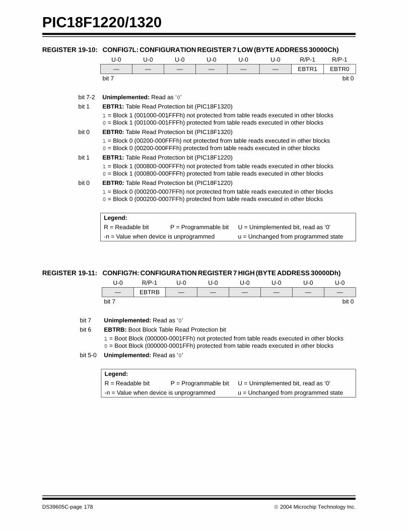
PIC18F1220/1320
REGISTER 19-10: CONFIG7L: CONFIGURATION REGISTER 7 LOW (BYTE ADDRESS 30000Ch)
REGISTER 19-11: CONFIG7H: CONFIGURATION REGISTER 7 HIGH (BYTE ADDRESS 30000Dh)
U-0 U-0 U-0 U-0 U-0 U-0 R/P-1 R/P-1
— — — — — — EBTR1 EBTR0
bit 7 bit 0
bit 7-2 Unimplemented: Read as ‘0’
bit 1 EBTR1: Table Read Protection bit (PIC18F1320)
1 = Block 1 (001000-001FFFh) not protected from table reads executed in other blocks0 = Block 1 (001000-001FFFh) protected from table reads executed in other blocks
bit 0 EBTR0: Table Read Protection bit (PIC18F1320)1 = Block 0 (00200-000FFFh) not protected from table reads executed in other blocks 0 = Block 0 (00200-000FFFh) protected from table reads executed in other blocks
bit 1 EBTR1: Table Read Protection bit (PIC18F1220)1 = Block 1 (000800-000FFFh) not protected from table reads executed in other blocks 0 = Block 1 (000800-000FFFh) protected from table reads executed in other blocks
bit 0 EBTR0: Table Read Protection bit (PIC18F1220)
1 = Block 0 (000200-0007FFh) not protected from table reads executed in other blocks 0 = Block 0 (000200-0007FFh) protected from table reads executed in other blocks
Legend:
R = Readable bit P = Programmable bit U = Unimplemented bit, read as ‘0’
-n = Value when device is unprogrammed u = Unchanged from programmed state
U-0 R/P-1 U-0 U-0 U-0 U-0 U-0 U-0
— EBTRB — — — — — —
bit 7 bit 0
bit 7 Unimplemented: Read as ‘0’
bit 6 EBTRB: Boot Block Table Read Protection bit
1 = Boot Block (000000-0001FFh) not protected from table reads executed in other blocks0 = Boot Block (000000-0001FFh) protected from table reads executed in other blocks
bit 5-0 Unimplemented: Read as ‘0’
Legend:
R = Readable bit P = Programmable bit U = Unimplemented bit, read as ‘0’
-n = Value when device is unprogrammed u = Unchanged from programmed state
DS39605C-page 178 2004 Microchip Technology Inc.

PIC18F1220/1320
REGISTER 19-12: DEVID1: DEVICE ID REGISTER 1 FOR PIC18F1220/1320 DEVICES
REGISTER 19-13: DEVID2: DEVICE ID REGISTER 2 FOR PIC18F1220/1320 DEVICES
R R R R R R R R
DEV2 DEV1 DEV0 REV4 REV3 REV2 REV1 REV0
bit 7 bit 0
bit 7-5 DEV2:DEV0: Device ID bits111 = PIC18F1220110 = PIC18F1320
bit 4-0 REV4:REV0: Revision ID bits
These bits are used to indicate the device revision.
Legend:
R = Read-only bit P = Programmable bit U = Unimplemented bit, read as ‘0’
-n = Value when device is unprogrammed u = Unchanged from programmed state
R R R R R R R R
DEV10 DEV9 DEV8 DEV7 DEV6 DEV5 DEV4 DEV3
bit 7 bit 0
bit 7-0 DEV10:DEV3: Device ID bitsThese bits are used with the DEV2:DEV0 bits in the Device ID Register 1 to identify the part number.0000 0111 = PIC18F1220/1320 devices
Note: These values for DEV10:DEV3 may be shared with other devices. The specificdevice is always identified by using the entire DEV10:DEV0 bit sequence.
Legend:
R = Read-only bit P = Programmable bit U = Unimplemented bit, read as ‘0’
-n = Value when device is unprogrammed u = Unchanged from programmed state
2004 Microchip Technology Inc. DS39605C-page 179
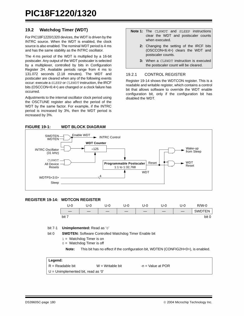
PIC18F1220/1320
19.2 Watchdog Timer (WDT)
For PIC18F1220/1320 devices, the WDT is driven by theINTRC source. When the WDT is enabled, the clocksource is also enabled. The nominal WDT period is 4 msand has the same stability as the INTRC oscillator.
The 4 ms period of the WDT is multiplied by a 16-bitpostscaler. Any output of the WDT postscaler is selectedby a multiplexer, controlled by bits in ConfigurationRegister 2H. Available periods range from 4 ms to131.072 seconds (2.18 minutes). The WDT andpostscaler are cleared when any of the following eventsoccur: execute a SLEEP or CLRWDT instruction, the IRCFbits (OSCCON<6:4>) are changed or a clock failure hasoccurred.
Adjustments to the internal oscillator clock period usingthe OSCTUNE register also affect the period of theWDT by the same factor. For example, if the INTRCperiod is increased by 3%, then the WDT period isincreased by 3%.
19.2.1 CONTROL REGISTER
Register 19-14 shows the WDTCON register. This is areadable and writable register, which contains a controlbit that allows software to override the WDT enableconfiguration bit, only if the configuration bit hasdisabled the WDT.
FIGURE 19-1: WDT BLOCK DIAGRAM
REGISTER 19-14: WDTCON REGISTER
Note 1: The CLRWDT and SLEEP instructionsclear the WDT and postscaler countswhen executed.
2: Changing the setting of the IRCF bits(OSCCON<6:4>) clears the WDT andpostscaler counts.
3: When a CLRWDT instruction is executedthe postscaler count will be cleared.
U-0 U-0 U-0 U-0 U-0 U-0 U-0 R/W-0
— — — — — — — SWDTEN
bit 7 bit 0
bit 7-1 Unimplemented: Read as ‘0’
bit 0 SWDTEN: Software Controlled Watchdog Timer Enable bit
1 = Watchdog Timer is on0 = Watchdog Timer is off
Note: This bit has no effect if the configuration bit, WDTEN (CONFIG2H<0>), is enabled.
Legend:
R = Readable bit W = Writable bit -n = Value at POR
U = Unimplemented bit, read as ‘0’
INTRC Oscillator
WDT
Wake-up
Reset
WDT
WDT Counter
(31 kHz)
Programmable Postscaler1:1 to 1:32,768
Enable WDT
WDTPS<3:0>
SWDTENWDTEN
CLRWDT
4
from Sleep
ResetAll Device
Sleep
INTRC Control
Resets
÷125
DS39605C-page 180 2004 Microchip Technology Inc.

PIC18F1220/1320
TABLE 19-2: SUMMARY OF WATCHDOG TIMER REGISTERS
19.3 Two-Speed Start-up
The Two-Speed Start-up feature helps to minimize thelatency period from oscillator start-up to code executionby allowing the microcontroller to use the INTRC oscil-lator as a clock source until the primary clock source isavailable. It is enabled by setting the IESO bit inConfiguration Register 1H (CONFIG1H<7>).
Two-Speed Start-up is available only if the primary oscil-lator mode is LP, XT, HS or HSPLL (crystal-basedmodes). Other sources do not require an OST start-updelay; for these, Two-Speed Start-up is disabled.
When enabled, Resets and wake-ups from Sleep modecause the device to configure itself to run from theinternal oscillator block as the clock source, followingthe time-out of the Power-up Timer after a Power-onReset is enabled. This allows almost immediate codeexecution while the primary oscillator starts and theOST is running. Once the OST times out, the deviceautomatically switches to PRI_RUN mode.
Because the OSCCON register is cleared on Resetevents, the INTOSC (or postscaler) clock source is notinitially available after a Reset event; the INTRC clockis used directly at its base frequency. To use a higherclock speed on wake-up, the INTOSC or postscalerclock sources can be selected to provide a higher clockspeed by setting bits, IFRC2:IFRC0, immediately afterReset. For wake-ups from Sleep, the INTOSC orpostscaler clock sources can be selected by settingIFRC2:IFRC0 prior to entering Sleep mode.
In all other power managed modes, Two-Speed Start-upis not used. The device will be clocked by the currentlyselected clock source until the primary clock sourcebecomes available. The setting of the IESO bit isignored.
19.3.1 SPECIAL CONSIDERATIONS FOR USING TWO-SPEED START-UP
While using the INTRC oscillator in Two-Speed Start-up, the device still obeys the normal commandsequences for entering power managed modes, includ-ing serial SLEEP instructions (refer to Section 3.1.3“Multiple Sleep Commands”). In practice, this meansthat user code can change the SCS1:SCS0 bit settingsand issue SLEEP commands before the OST times out.This would allow an application to briefly wake-up, per-form routine “housekeeping” tasks and return to Sleepbefore the device starts to operate from the primaryoscillator.
User code can also check if the primary clock source iscurrently providing the system clocking by checking thestatus of the OSTS bit (OSCCON<3>). If the bit is set,the primary oscillator is providing the system clock.Otherwise, the internal oscillator block is providing theclock during wake-up from Reset or Sleep mode.
FIGURE 19-2: TIMING TRANSITION FOR TWO-SPEED START-UP (INTOSC TO HSPLL)
Name Bit 7 Bit 6 Bit 5 Bit 4 Bit 3 Bit 2 Bit 1 Bit 0
CONFIG2H — — — WDTPS3 WDTPS2 WDTPS2 WDTPS0 WDTEN
RCON IPEN — — RI TO PD POR BOR
WDTCON — — — — — — — SWDTEN
Legend: Shaded cells are not used by the Watchdog Timer.
Q1 Q3 Q4
OSC1
Peripheral
Program PC PC + 2
INTOSC
PLL Clock
Q1
PC + 6
Q2
Output
Q3 Q4 Q1
CPU Clock
PC + 4
Clock
Counter
Q2 Q2 Q3 Q4
Note 1: TOST = 1024 TOSC; TPLL = 2 ms (approx). These intervals are not shown to scale.
Wake from Interrupt Event
TPLL(1)
1 2 3 4 5 6 7 8Clock Transition
OSTS bit Set
Multiplexer
TOST(1)
2004 Microchip Technology Inc. DS39605C-page 181
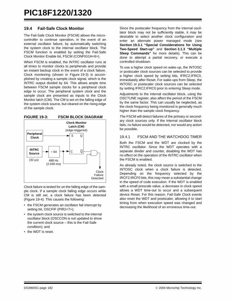
PIC18F1220/1320
19.4 Fail-Safe Clock Monitor
The Fail-Safe Clock Monitor (FSCM) allows the micro-controller to continue operation, in the event of anexternal oscillator failure, by automatically switchingthe system clock to the internal oscillator block. TheFSCM function is enabled by setting the Fail-SafeClock Monitor Enable bit, FSCM (CONFIG1H<6>).
When FSCM is enabled, the INTRC oscillator runs atall times to monitor clocks to peripherals and providean instant backup clock in the event of a clock failure.Clock monitoring (shown in Figure 19-3) is accom-plished by creating a sample clock signal, which is theINTRC output divided by 64. This allows ample timebetween FSCM sample clocks for a peripheral clockedge to occur. The peripheral system clock and thesample clock are presented as inputs to the ClockMonitor latch (CM). The CM is set on the falling edge ofthe system clock source, but cleared on the rising edgeof the sample clock.
FIGURE 19-3: FSCM BLOCK DIAGRAM
Clock failure is tested for on the falling edge of the sam-ple clock. If a sample clock falling edge occurs whileCM is still set, a clock failure has been detected(Figure 19-4). This causes the following:
• the FSCM generates an oscillator fail interrupt by setting bit, OSCFIF (PIR2<7>);
• the system clock source is switched to the internal oscillator block (OSCCON is not updated to show the current clock source – this is the Fail-Safe condition); and
• the WDT is reset.
Since the postscaler frequency from the internal oscil-lator block may not be sufficiently stable, it may bedesirable to select another clock configuration andenter an alternate power managed mode (seeSection 19.3.1 “Special Considerations for UsingTwo-Speed Start-up” and Section 3.1.3 “MultipleSleep Commands” for more details). This can bedone to attempt a partial recovery, or execute acontrolled shutdown.
To use a higher clock speed on wake-up, the INTOSCor postscaler clock sources can be selected to providea higher clock speed by setting bits, IFRC2:IFRC0,immediately after Reset. For wake-ups from Sleep, theINTOSC or postscaler clock sources can be selectedby setting IFRC2:IFRC0 prior to entering Sleep mode.
Adjustments to the internal oscillator block, using theOSCTUNE register, also affect the period of the FSCMby the same factor. This can usually be neglected, asthe clock frequency being monitored is generally muchhigher than the sample clock frequency.
The FSCM will detect failures of the primary or second-ary clock sources only. If the internal oscillator blockfails, no failure would be detected, nor would any actionbe possible.
19.4.1 FSCM AND THE WATCHDOG TIMER
Both the FSCM and the WDT are clocked by theINTRC oscillator. Since the WDT operates with aseparate divider and counter, disabling the WDT hasno effect on the operation of the INTRC oscillator whenthe FSCM is enabled.
As already noted, the clock source is switched to theINTOSC clock when a clock failure is detected.Depending on the frequency selected by theIRCF2:IRCF0 bits, this may mean a substantial changein the speed of code execution. If the WDT is enabledwith a small prescale value, a decrease in clock speedallows a WDT time-out to occur and a subsequentdevice Reset. For this reason, Fail-Safe Clock eventsalso reset the WDT and postscaler, allowing it to starttiming from when execution speed was changed anddecreasing the likelihood of an erroneous time-out.
Peripheral
INTRC÷ 64
S
C
Q
(32 µs) 488 Hz(2.048 ms)
Clock MonitorLatch (CM)
(edge-triggered)
ClockFailure
Detected
Source
Clock
Q
DS39605C-page 182 2004 Microchip Technology Inc.

PIC18F1220/1320
19.4.2 EXITING FAIL-SAFE OPERATION
The Fail-Safe condition is terminated by either a deviceReset, or by entering a power managed mode. OnReset, the controller starts the primary clock sourcespecified in Configuration Register 1H (with anyrequired start-up delays that are required for theoscillator mode, such as OST or PLL timer). TheINTOSC multiplexer provides the system clock until theprimary clock source becomes ready (similar to a Two-Speed Start-up). The clock system source is thenswitched to the primary clock (indicated by the OSTSbit in the OSCCON register becoming set). The Fail-Safe Clock Monitor then resumes monitoring theperipheral clock.
The primary clock source may never become readyduring start-up. In this case, operation is clocked by theINTOSC multiplexer. The OSCCON register will remainin its Reset state until a power managed mode isentered.
Entering a power managed mode by loading theOSCCON register and executing a SLEEP instructionwill clear the Fail-Safe condition. When the Fail-Safecondition is cleared, the clock monitor will resumemonitoring the peripheral clock.
19.4.3 FSCM INTERRUPTS IN POWER MANAGED MODES
As previously mentioned, entering a power managedmode clears the Fail-Safe condition. By entering apower managed mode, the clock multiplexer selectsthe clock source selected by the OSCCON register.Fail-Safe monitoring of the power managed clocksource resumes in the power managed mode.
If an oscillator failure occurs during power managedoperation, the subsequent events depend on whetheror not the oscillator failure interrupt is enabled. Ifenabled (OSCFIF = 1), code execution will be clockedby the INTOSC multiplexer. An automatic transitionback to the failed clock source will not occur.
If the interrupt is disabled, the device will not exit thepower managed mode on oscillator failure. Instead, thedevice will continue to operate as before, but clockedby the INTOSC multiplexer. While in Idle mode, subse-quent interrupts will cause the CPU to begin executinginstructions while being clocked by the INTOSC multi-plexer. The device will not transition to a different clocksource until the Fail-Safe condition is cleared.
FIGURE 19-4: FSCM TIMING DIAGRAM
OSCFIF
CM Output
SystemClock
Output
Sample Clock
FailureDetected
OscillatorFailure
Note: The system clock is normally at a much higher frequency than the sample clock. The relative frequencies inthis example have been chosen for clarity.
(Q)
CM Test CM Test CM Test
2004 Microchip Technology Inc. DS39605C-page 183
PIC18F1220/1320
19.4.4 POR OR WAKE FROM SLEEP
The FSCM is designed to detect oscillator failure at anypoint after the device has exited Power-on Reset(POR) or Low-Power Sleep mode. When the primarysystem clock is EC, RC or INTRC modes, monitoringcan begin immediately following these events.
For oscillator modes involving a crystal or resonator(HS, HSPLL, LP or XT), the situation is somewhat dif-ferent. Since the oscillator may require a start-up timeconsiderably longer than the FCSM sample clock time,a false clock failure may be detected. To prevent this,the internal oscillator block is automatically configuredas the system clock and functions until the primaryclock is stable (the OST and PLL timers have timedout). This is identical to Two-Speed Start-up mode.Once the primary clock is stable, the INTRC returns toits role as the FSCM source
As noted in Section 19.3.1 “Special Considerationsfor Using Two-Speed Start-up”, it is also possible toselect another clock configuration and enter an alter-nate power managed mode while waiting for theprimary system clock to become stable. When the newpowered managed mode is selected, the primary clockis disabled.
Note: The same logic that prevents false oscilla-tor failure interrupts on POR or wake fromSleep will also prevent the detection of theoscillator’s failure to start at all followingthese events. This can be avoided bymonitoring the OSTS bit and using atiming routine to determine if the oscillatoris taking too long to start. Even so, nooscillator failure interrupt will be flagged.
DS39605C-page 184 2004 Microchip Technology Inc.
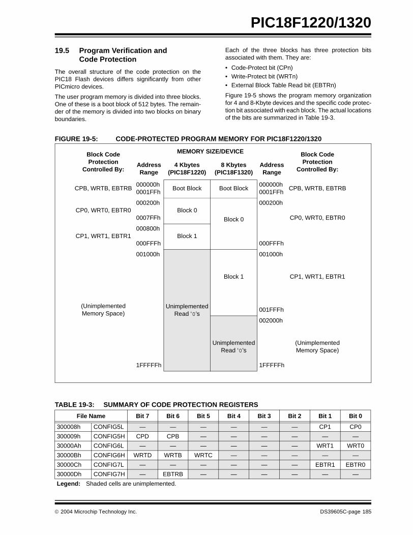
PIC18F1220/1320
19.5 Program Verification and Code Protection
The overall structure of the code protection on thePIC18 Flash devices differs significantly from otherPICmicro devices.
The user program memory is divided into three blocks.One of these is a boot block of 512 bytes. The remain-der of the memory is divided into two blocks on binaryboundaries.
Each of the three blocks has three protection bitsassociated with them. They are:
• Code-Protect bit (CPn)• Write-Protect bit (WRTn)• External Block Table Read bit (EBTRn)
Figure 19-5 shows the program memory organizationfor 4 and 8-Kbyte devices and the specific code protec-tion bit associated with each block. The actual locationsof the bits are summarized in Table 19-3.
FIGURE 19-5: CODE-PROTECTED PROGRAM MEMORY FOR PIC18F1220/1320
TABLE 19-3: SUMMARY OF CODE PROTECTION REGISTERS
Block Code Protection
Controlled By:
MEMORY SIZE/DEVICE Block Code Protection
Controlled By:Address Range
4 Kbytes(PIC18F1220)
8 Kbytes(PIC18F1320)
Address Range
CPB, WRTB, EBTRB000000h0001FFh
Boot Block Boot Block000000h0001FFh
CPB, WRTB, EBTRB
CP0, WRT0, EBTR0000200h
0007FFhBlock 0
Block 0
000200h
CP0, WRT0, EBTR0
CP1, WRT1, EBTR1000800h
000FFFhBlock 1
000FFFh
(Unimplemented Memory Space)
001000h
UnimplementedRead ‘0’s
Block 1
001000h
CP1, WRT1, EBTR1
001FFFh
1FFFFFh
UnimplementedRead ‘0’s
002000h
1FFFFFh
(Unimplemented Memory Space)
File Name Bit 7 Bit 6 Bit 5 Bit 4 Bit 3 Bit 2 Bit 1 Bit 0
300008h CONFIG5L — — — — — — CP1 CP0
300009h CONFIG5H CPD CPB — — — — — —
30000Ah CONFIG6L — — — — — — WRT1 WRT0
30000Bh CONFIG6H WRTD WRTB WRTC — — — — —
30000Ch CONFIG7L — — — — — — EBTR1 EBTR0
30000Dh CONFIG7H — EBTRB — — — — — —
Legend: Shaded cells are unimplemented.
2004 Microchip Technology Inc. DS39605C-page 185
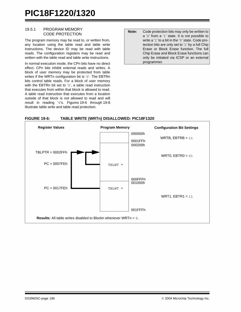
PIC18F1220/1320
19.5.1 PROGRAM MEMORYCODE PROTECTION
The program memory may be read to, or written from,any location using the table read and table writeinstructions. The device ID may be read with tablereads. The configuration registers may be read andwritten with the table read and table write instructions.
In normal execution mode, the CPn bits have no directeffect. CPn bits inhibit external reads and writes. Ablock of user memory may be protected from tablewrites if the WRTn configuration bit is ‘0’. The EBTRnbits control table reads. For a block of user memorywith the EBTRn bit set to ‘0’, a table read instructionthat executes from within that block is allowed to read.A table read instruction that executes from a locationoutside of that block is not allowed to read and willresult in reading ‘0’s. Figures 19-6 through 19-8illustrate table write and table read protection.
FIGURE 19-6: TABLE WRITE (WRTn) DISALLOWED: PIC18F1320
Note: Code protection bits may only be written toa ‘0’ from a ‘1’ state. It is not possible towrite a ‘1’ to a bit in the ‘0’ state. Code pro-tection bits are only set to ‘1’ by a full ChipErase or Block Erase function. The fullChip Erase and Block Erase functions canonly be initiated via ICSP or an externalprogrammer.
000000h
0001FFh000200h
000FFFh001000h
001FFFh
WRTB, EBTRB = 11
WRT0, EBTR0 = 01
TBLWT *
TBLPTR = 0002FFh
PC = 0007FEh
TBLWT *PC = 0017FEh
Register Values Program Memory Configuration Bit Settings
Results: All table writes disabled to Blockn whenever WRTn = 0.
WRT1, EBTR1 = 11
DS39605C-page 186 2004 Microchip Technology Inc.
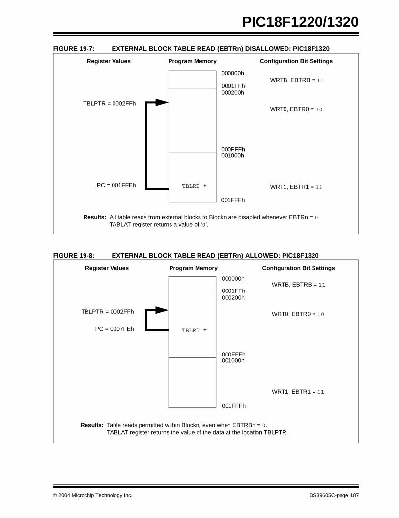
PIC18F1220/1320
FIGURE 19-7: EXTERNAL BLOCK TABLE READ (EBTRn) DISALLOWED: PIC18F1320
FIGURE 19-8: EXTERNAL BLOCK TABLE READ (EBTRn) ALLOWED: PIC18F1320
000000h
0001FFh000200h
000FFFh001000h
001FFFh
WRTB, EBTRB = 11
WRT0, EBTR0 = 10
WRT1, EBTR1 = 11
TBLPTR = 0002FFh
Register Values Program Memory Configuration Bit Settings
PC = 001FFEh TBLRD *
Results: All table reads from external blocks to Blockn are disabled whenever EBTRn = 0. TABLAT register returns a value of ‘0’.
000000h
0001FFh000200h
000FFFh001000h
001FFFh
WRTB, EBTRB = 11
WRT0, EBTR0 = 10
WRT1, EBTR1 = 11
TBLRD *
TBLPTR = 0002FFh
PC = 0007FEh
Register Values Program Memory Configuration Bit Settings
Results: Table reads permitted within Blockn, even when EBTRBn = 0. TABLAT register returns the value of the data at the location TBLPTR.
2004 Microchip Technology Inc. DS39605C-page 187
PIC18F1220/1320
19.5.2 DATA EEPROM CODE PROTECTION
The entire data EEPROM is protected from externalreads and writes by two bits: CPD and WRTD. CPDinhibits external reads and writes of data EEPROM.WRTD inhibits external writes to data EEPROM. TheCPU can continue to read and write data EEPROM,regardless of the protection bit settings.
19.5.3 CONFIGURATION REGISTER PROTECTION
The configuration registers can be write-protected. TheWRTC bit controls protection of the configurationregisters. In normal execution mode, the WRTC bit isreadable only. WRTC can only be written via ICSP oran external programmer.
19.6 ID Locations
Eight memory locations (200000h-200007h) aredesignated as ID locations, where the user can storechecksum or other code identification numbers. Theselocations are both readable and writable during normalexecution through the TBLRD and TBLWT instructions,or during program/verify. The ID locations can be readwhen the device is code-protected.
19.7 In-Circuit Serial Programming
PIC18F1220/1320 microcontrollers can be seriallyprogrammed while in the end application circuit. This issimply done with two lines for clock and data and threeother lines for power, ground and the programmingvoltage. This allows customers to manufacture boardswith unprogrammed devices and then program themicrocontroller just before shipping the product. Thisalso allows the most recent firmware or a customfirmware to be programmed (see Table 19-4).
19.8 In-Circuit Debugger
When the DEBUG bit in configuration register,CONFIG4L, is programmed to a ‘0’, the In-CircuitDebugger functionality is enabled. This function allowssimple debugging functions when used with MPLAB®
IDE. When the microcontroller has this featureenabled, some resources are not available for generaluse. Table 19-5 shows which resources are required bythe background debugger.
TABLE 19-5: DEBUGGER RESOURCES
To use the In-Circuit Debugger function of themicrocontroller, the design must implement In-CircuitSerial Programming connections to MCLR/VPP, VDD,VSS, RB7 and RB6. This will interface to the In-CircuitDebugger module available from Microchip, or one of thethird party development tool companies (see the note fol-lowing Section 19.7 “In-Circuit Serial Programming”for more information).
Note: The Timer1 oscillator shares the T1OSIand T1OSO pins with the PGD and PGCpins used for programming anddebugging.
When using the Timer1 oscillator, In-CircuitSerial Programming (ICSP) may notfunction correctly (high voltage or lowvoltage), or the In-Circuit Debugger (ICD)may not communicate with the controller.As a result of using either ICSP or ICD, theTimer1 crystal may be damaged.
If ICSP or ICD operations are required, thecrystal should be disconnected from thecircuit (disconnect either lead), or installedafter programming. The oscillator loadingcapacitors may remain in-circuit duringICSP or ICD operation.
TABLE 19-4: ICSP/ICD CONNECTIONSSignal Pin Notes
PGD RB7/PGD/T1OSI/P1D/KBI3
Shared with T1OSC – protect crystal
PGC RB6/PGC/T1OSO/T13CKI/P1C/KBI2
Shared with T1OSC – protect crystal
MCLR MCLR/VPP/RA5
VDD VDD
VSS VSS
PGM RB5/PGM/KBI1 Optional – pull RB5 low is LVP enabled
I/O pins: RB6, RB7
Stack: 2 levels
Program Memory: 512 bytes
Data Memory: 10 bytes
DS39605C-page 188 2004 Microchip Technology Inc.
PIC18F1220/1320
19.9 Low-Voltage ICSP Programming
The LVP bit in configuration register, CONFIG4L,enables Low-Voltage Programming (LVP). When LVPis enabled, the microcontroller can be programmedwithout requiring high voltage being applied to theMCLR/VPP/RA5 pin, but the RB5/PGM/KBI1 pin is thendedicated to controlling Program mode entry and is notavailable as a general purpose I/O pin.
LVP is enabled in erased devices.
While programming using LVP, VDD is applied to theMCLR/VPP/RA5 pin as in normal execution mode. Toenter Programming mode, VDD is applied to the PGMpin.
If Low-Voltage Programming mode will not be used, theLVP bit can be cleared and RB5/PGM/KBI1 becomesavailable as the digital I/O pin RB5. The LVP bit may beset or cleared only when using standard high-voltageprogramming (VIHH applied to the MCLR/VPP/RA5 pin).Once LVP has been disabled, only the standard high-voltage programming is available and must be used toprogram the device.
Memory that is not code-protected can be erased,using either a Block Erase, or erased row by row, thenwritten at any specified VDD. If code-protected memoryis to be erased, a Block Erase is required. If a BlockErase is to be performed when using Low-VoltageProgramming, the device must be supplied with VDD of4.5V to 5.5V.
Note 1: High-voltage programming is alwaysavailable, regardless of the state of theLVP bit or the PGM pin, by applying VIHH
to the MCLR pin.
2: When Low-Voltage Programming isenabled, the RB5 pin can no longer beused as a general purpose I/O pin.
3: When LVP is enabled, externally pull thePGM pin to VSS to allow normal programexecution.
2004 Microchip Technology Inc. DS39605C-page 189

PIC18F1220/1320
NOTES:
DS39605C-page 190 2004 Microchip Technology Inc.
PIC18F1220/1320
20.0 INSTRUCTION SET SUMMARY
The PIC18 instruction set adds many enhancements tothe previous PICmicro instruction sets, while maintainingan easy migration from these PICmicro instruction sets.
Most instructions are a single program memory word(16 bits), but there are three instructions that requiretwo program memory locations.
Each single-word instruction is a 16-bit word dividedinto an opcode, which specifies the instruction type andone or more operands, which further specify theoperation of the instruction.
The instruction set is highly orthogonal and is groupedinto four basic categories:
• Byte-oriented operations• Bit-oriented operations
• Literal operations• Control operations
The PIC18 instruction set summary in Table 20-1 listsbyte-oriented, bit-oriented, literal and controloperations. Table 20-1 shows the opcode fielddescriptions.
Most byte-oriented instructions have three operands:
1. The file register (specified by ‘f’) 2. The destination of the result
(specified by ‘d’) 3. The accessed memory
(specified by ‘a’)
The file register designator ‘f’ specifies which fileregister is to be used by the instruction.
The destination designator ‘d’ specifies where theresult of the operation is to be placed. If ‘d’ is zero, theresult is placed in the WREG register. If ‘d’ is one, theresult is placed in the file register specified in theinstruction.
All bit-oriented instructions have three operands:
1. The file register (specified by ‘f’)
2. The bit in the file register (specified by ‘b’)
3. The accessed memory (specified by ‘a’)
The bit field designator ‘b’ selects the number of the bitaffected by the operation, while the file register desig-nator ‘f’ represents the number of the file in which thebit is located.
The literal instructions may use some of the followingoperands:
• A literal value to be loaded into a file register (specified by ‘k’)
• The desired FSR register to load the literal value into (specified by ‘f’)
• No operand required (specified by ‘—’)
The control instructions may use some of the followingoperands:
• A program memory address (specified by ‘n’)• The mode of the CALL or RETURN instructions
(specified by ‘s’)• The mode of the table read and table write
instructions (specified by ‘m’)• No operand required
(specified by ‘—’)
All instructions are a single word, except for threedouble-word instructions. These three instructionswere made double-word instructions so that all therequired information is available in these 32 bits. In thesecond word, the 4 MSbs are ‘1’s. If this second wordis executed as an instruction (by itself), it will executeas a NOP.
All single-word instructions are executed in a singleinstruction cycle, unless a conditional test is true, or theprogram counter is changed as a result of the instruc-tion. In these cases, the execution takes two instructioncycles, with the additional instruction cycle(s) executedas a NOP.
The double-word instructions execute in two instructioncycles.
One instruction cycle consists of four oscillator periods.Thus, for an oscillator frequency of 4 MHz, the normalinstruction execution time is 1 µs. If a conditional test istrue, or the program counter is changed as a result ofan instruction, the instruction execution time is 2 µs.Two-word branch instructions (if true) would take 3 µs.
Figure 20-1 shows the general formats that theinstructions can have.
All examples use the format ‘nnh’ to represent a hexa-decimal number, where ‘h’ signifies a hexadecimaldigit.
The Instruction Set Summary, shown in Table 20-1,lists the instructions recognized by the MicrochipAssembler (MPASMTM). Section 20.2 “InstructionSet” provides a description of each instruction.
20.1 Read-Modify-Write Operations
Any instruction that specifies a file register as part ofthe instruction performs a Read-Modify-Write (R-M-W)operation. The register is read, the data is modified andthe result is stored according to either the instruction orthe destination designator ‘d’. A read operation isperformed on a register even if the instruction writes tothat register.
For example, a “BCF PORTB,1” instruction will readPORTB, clear bit 1 of the data, then write the resultback to PORTB. The read operation would have theunintended result that any condition that sets the RBIFflag would be cleared. The R-M-W operation may alsocopy the level of an input pin to its corresponding outputlatch.
2004 Microchip Technology Inc. DS39605C-page 191
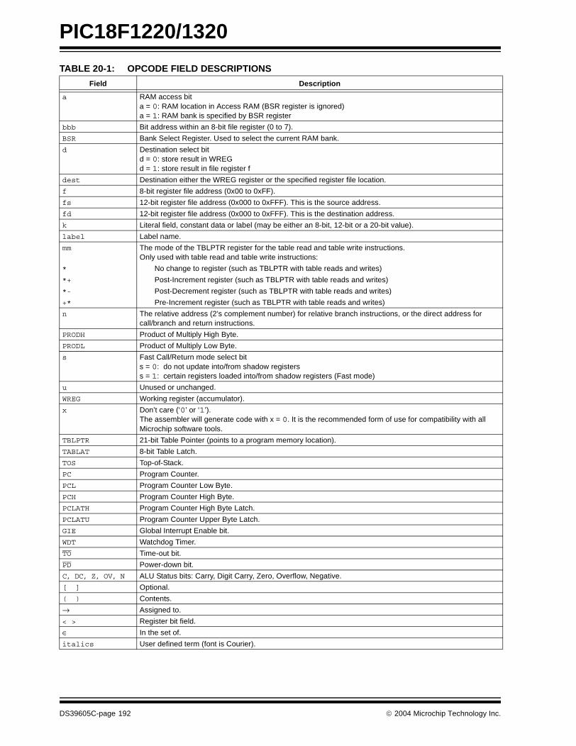
PIC18F1220/1320
TABLE 20-1: OPCODE FIELD DESCRIPTIONS
Field Description
a RAM access bita = 0: RAM location in Access RAM (BSR register is ignored)a = 1: RAM bank is specified by BSR register
bbb Bit address within an 8-bit file register (0 to 7).
BSR Bank Select Register. Used to select the current RAM bank.
d Destination select bitd = 0: store result in WREGd = 1: store result in file register f
dest Destination either the WREG register or the specified register file location.
f 8-bit register file address (0x00 to 0xFF).
fs 12-bit register file address (0x000 to 0xFFF). This is the source address.
fd 12-bit register file address (0x000 to 0xFFF). This is the destination address.
k Literal field, constant data or label (may be either an 8-bit, 12-bit or a 20-bit value).
label Label name.
mm The mode of the TBLPTR register for the table read and table write instructions.Only used with table read and table write instructions:
* No change to register (such as TBLPTR with table reads and writes)
*+ Post-Increment register (such as TBLPTR with table reads and writes)
*- Post-Decrement register (such as TBLPTR with table reads and writes)
+* Pre-Increment register (such as TBLPTR with table reads and writes)
n The relative address (2’s complement number) for relative branch instructions, or the direct address for call/branch and return instructions.
PRODH Product of Multiply High Byte.
PRODL Product of Multiply Low Byte.
s Fast Call/Return mode select bits = 0: do not update into/from shadow registerss = 1: certain registers loaded into/from shadow registers (Fast mode)
u Unused or unchanged.
WREG Working register (accumulator).
x Don’t care (‘0’ or ‘1’). The assembler will generate code with x = 0. It is the recommended form of use for compatibility with all Microchip software tools.
TBLPTR 21-bit Table Pointer (points to a program memory location).
TABLAT 8-bit Table Latch.
TOS Top-of-Stack.
PC Program Counter.
PCL Program Counter Low Byte.
PCH Program Counter High Byte.
PCLATH Program Counter High Byte Latch.
PCLATU Program Counter Upper Byte Latch.
GIE Global Interrupt Enable bit.
WDT Watchdog Timer.
TO Time-out bit.
PD Power-down bit.
C, DC, Z, OV, N ALU Status bits: Carry, Digit Carry, Zero, Overflow, Negative.
[ ] Optional.
( ) Contents.
→ Assigned to.
< > Register bit field.
∈ In the set of.
italics User defined term (font is Courier).
DS39605C-page 192 2004 Microchip Technology Inc.

PIC18F1220/1320
FIGURE 20-1: GENERAL FORMAT FOR INSTRUCTIONS
Byte-oriented file register operations
15 10 9 8 7 0
d = 0 for result destination to be WREG register
OPCODE d a f (FILE #)
d = 1 for result destination to be file register (f)a = 0 to force Access Bank
Bit-oriented file register operations
15 12 11 9 8 7 0
OPCODE b (BIT #) a f (FILE #)
b = 3-bit position of bit in file register (f)
Literal operations
15 8 7 0
OPCODE k (literal)
k = 8-bit immediate value
Byte to Byte move operations (2-word)
15 12 11 0
OPCODE f (Source FILE #)
CALL, GOTO and Branch operations
15 8 7 0
OPCODE n<7:0> (literal)
n = 20-bit immediate value
a = 1 for BSR to select bankf = 8-bit file register address
a = 0 to force Access Banka = 1 for BSR to select bankf = 8-bit file register address
15 12 11 0
1111 n<19:8> (literal)
15 12 11 0
1111 f (Destination FILE #)
f = 12-bit file register address
Control operations
Example Instruction
ADDWF MYREG, W, B
MOVFF MYREG1, MYREG2
BSF MYREG, bit, B
MOVLW 0x7F
GOTO Label
15 8 7 0
OPCODE n<7:0> (literal)
15 12 11 0
n<19:8> (literal)
CALL MYFUNC
15 11 10 0
OPCODE n<10:0> (literal)
S = Fast bit
BRA MYFUNC
15 8 7 0
OPCODE n<7:0> (literal) BC MYFUNC
S
2004 Microchip Technology Inc. DS39605C-page 193
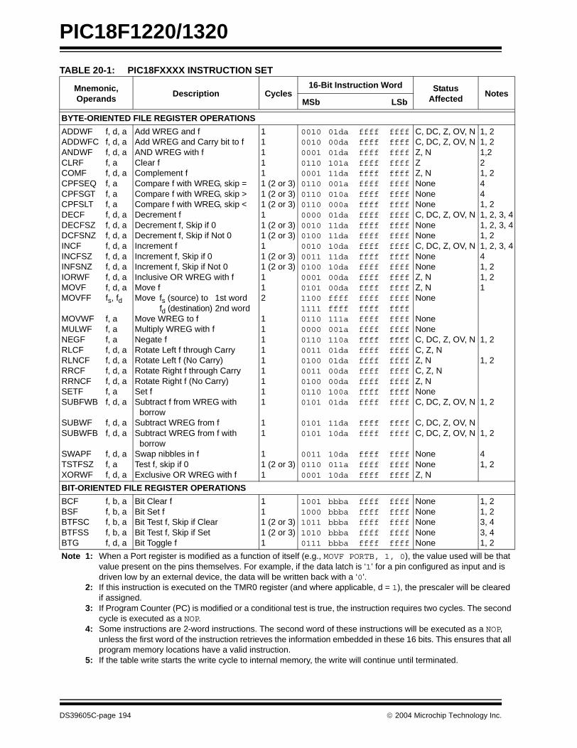
PIC18F1220/1320
TABLE 20-1: PIC18FXXXX INSTRUCTION SET
Mnemonic,Operands
Description Cycles16-Bit Instruction Word Status
AffectedNotes
MSb LSb
BYTE-ORIENTED FILE REGISTER OPERATIONS
ADDWFADDWFCANDWFCLRFCOMFCPFSEQCPFSGTCPFSLTDECFDECFSZDCFSNZINCFINCFSZINFSNZIORWFMOVFMOVFF
MOVWFMULWFNEGFRLCFRLNCFRRCFRRNCFSETFSUBFWB
SUBWFSUBWFB
SWAPFTSTFSZXORWF
f, d, af, d, af, d, af, af, d, af, af, af, af, d, af, d, af, d, af, d, af, d, af, d, af, d, af, d, afs, fd
f, af, af, af, d, af, d, af, d, af, d, af, af, d, a
f, d, af, d, a
f, d, af, af, d, a
Add WREG and fAdd WREG and Carry bit to fAND WREG with fClear fComplement fCompare f with WREG, skip =Compare f with WREG, skip >Compare f with WREG, skip <Decrement fDecrement f, Skip if 0Decrement f, Skip if Not 0Increment fIncrement f, Skip if 0Increment f, Skip if Not 0Inclusive OR WREG with fMove fMove fs (source) to 1st word
fd (destination) 2nd wordMove WREG to fMultiply WREG with fNegate fRotate Left f through CarryRotate Left f (No Carry)Rotate Right f through CarryRotate Right f (No Carry)Set fSubtract f from WREG with borrow Subtract WREG from fSubtract WREG from f with borrowSwap nibbles in fTest f, skip if 0Exclusive OR WREG with f
111111 (2 or 3)1 (2 or 3)1 (2 or 3)11 (2 or 3)1 (2 or 3)11 (2 or 3)1 (2 or 3)112
111111111
11
11 (2 or 3)1
001000100001011000010110011001100000001001000010001101000001010111001111011000000110001101000011010001100101
01010101
001101100001
01da00da01da101a11da001a010a000a01da11da11da10da11da10da00da00daffffffff111a001a110a01da01da00da00da100a01da
11da10da
10da011a10da
ffffffffffffffffffffffffffffffffffffffffffffffffffffffffffffffffffffffffffffffffffffffffffffffffffffffffffff
ffffffff
ffffffffffff
ffffffffffffffffffffffffffffffffffffffffffffffffffffffffffffffffffffffffffffffffffffffffffffffffffffffffffff
ffffffff
ffffffffffff
C, DC, Z, OV, NC, DC, Z, OV, NZ, NZZ, NNoneNoneNoneC, DC, Z, OV, NNoneNoneC, DC, Z, OV, NNoneNoneZ, NZ, NNone
NoneNoneC, DC, Z, OV, NC, Z, NZ, NC, Z, NZ, NNoneC, DC, Z, OV, N
C, DC, Z, OV, NC, DC, Z, OV, N
NoneNoneZ, N
1, 21, 21,221, 2441, 21, 2, 3, 41, 2, 3, 41, 21, 2, 3, 441, 21, 21
1, 2
1, 2
1, 2
1, 2
41, 2
BIT-ORIENTED FILE REGISTER OPERATIONS
BCFBSFBTFSCBTFSSBTG
f, b, af, b, af, b, af, b, af, d, a
Bit Clear fBit Set fBit Test f, Skip if ClearBit Test f, Skip if SetBit Toggle f
111 (2 or 3)1 (2 or 3)1
10011000101110100111
bbbabbbabbbabbbabbba
ffffffffffffffffffff
ffffffffffffffffffff
NoneNoneNoneNoneNone
1, 21, 23, 43, 41, 2
Note 1: When a Port register is modified as a function of itself (e.g., MOVF PORTB, 1, 0), the value used will be that value present on the pins themselves. For example, if the data latch is ‘1’ for a pin configured as input and is driven low by an external device, the data will be written back with a ‘0’.
2: If this instruction is executed on the TMR0 register (and where applicable, d = 1), the prescaler will be cleared if assigned.
3: If Program Counter (PC) is modified or a conditional test is true, the instruction requires two cycles. The secondcycle is executed as a NOP.
4: Some instructions are 2-word instructions. The second word of these instructions will be executed as a NOP, unless the first word of the instruction retrieves the information embedded in these 16 bits. This ensures that allprogram memory locations have a valid instruction.
5: If the table write starts the write cycle to internal memory, the write will continue until terminated.
DS39605C-page 194 2004 Microchip Technology Inc.

PIC18F1220/1320
CONTROL OPERATIONS
BCBNBNCBNNBNOVBNZBOVBRABZCALL
CLRWDTDAWGOTO
NOPNOPPOPPUSHRCALLRESETRETFIE
RETLWRETURNSLEEP
nnnnnnnnnn, s
——n
————n
s
ks—
Branch if CarryBranch if NegativeBranch if Not CarryBranch if Not NegativeBranch if Not OverflowBranch if Not ZeroBranch if OverflowBranch Unconditionally Branch if ZeroCall subroutine 1st word
2nd wordClear Watchdog TimerDecimal Adjust WREGGo to address 1st word
2nd wordNo OperationNo OperationPop top of return stack (TOS)Push top of return stack (TOS)Relative CallSoftware device ResetReturn from interrupt enable
Return with literal in WREG Return from SubroutineGo into Standby mode
1 (2)1 (2)1 (2)1 (2)1 (2)1 (2)1 (2)21 (2)2
112
1111212
221
1110111011101110111011101110110111101110111100000000111011110000111100000000110100000000
000000000000
00100110001101110101000101000nnn0000110skkkk000000001111kkkk0000xxxx000000001nnn00000000
110000000000
nnnnnnnnnnnnnnnnnnnnnnnnnnnnnnnnnnnnkkkkkkkk00000000kkkkkkkk0000xxxx00000000nnnn11110001
kkkk00010000
nnnnnnnnnnnnnnnnnnnnnnnnnnnnnnnnnnnnkkkkkkkk01000111kkkkkkkk0000xxxx01100101nnnn1111000s
kkkk001s0011
NoneNoneNoneNoneNoneNoneNoneNoneNoneNone
TO, PDCNone
NoneNoneNoneNoneNoneAllGIE/GIEH, PEIE/GIELNoneNoneTO, PD
4
TABLE 20-1: PIC18FXXXX INSTRUCTION SET (CONTINUED)
Mnemonic,Operands
Description Cycles16-Bit Instruction Word Status
AffectedNotes
MSb LSb
Note 1: When a Port register is modified as a function of itself (e.g., MOVF PORTB, 1, 0), the value used will be that value present on the pins themselves. For example, if the data latch is ‘1’ for a pin configured as input and is driven low by an external device, the data will be written back with a ‘0’.
2: If this instruction is executed on the TMR0 register (and where applicable, d = 1), the prescaler will be cleared if assigned.
3: If Program Counter (PC) is modified or a conditional test is true, the instruction requires two cycles. The secondcycle is executed as a NOP.
4: Some instructions are 2-word instructions. The second word of these instructions will be executed as a NOP, unless the first word of the instruction retrieves the information embedded in these 16 bits. This ensures that allprogram memory locations have a valid instruction.
5: If the table write starts the write cycle to internal memory, the write will continue until terminated.
2004 Microchip Technology Inc. DS39605C-page 195

PIC18F1220/1320
LITERAL OPERATIONS
ADDLWANDLWIORLWLFSR
MOVLBMOVLWMULLWRETLWSUBLWXORLW
kkkf, k
kkkkkk
Add literal and WREGAND literal with WREGInclusive OR literal with WREGMove literal (12-bit) 2nd word to FSRx 1st wordMove literal to BSR<3:0>Move literal to WREGMultiply literal with WREGReturn with literal in WREG Subtract WREG from literalExclusive OR literal with WREG
1112
111211
00000000000011101111000000000000000000000000
11111011100111100000000111101101110010001010
kkkkkkkkkkkk00ffkkkk0000kkkkkkkkkkkkkkkkkkkk
kkkkkkkkkkkkkkkkkkkkkkkkkkkkkkkkkkkkkkkkkkkk
C, DC, Z, OV, NZ, NZ, NNone
NoneNoneNoneNoneC, DC, Z, OV, NZ, N
DATA MEMORY ↔ PROGRAM MEMORY OPERATIONS
TBLRD*TBLRD*+TBLRD*-TBLRD+*TBLWT*TBLWT*+TBLWT*-TBLWT+*
Table readTable read with post-incrementTable read with post-decrementTable read with pre-incrementTable writeTable write with post-incrementTable write with post-decrementTable write with pre-increment
2
2 (5)
00000000000000000000000000000000
00000000000000000000000000000000
00000000000000000000000000000000
10001001101010111100110111101111
NoneNoneNoneNoneNoneNoneNoneNone
TABLE 20-1: PIC18FXXXX INSTRUCTION SET (CONTINUED)
Mnemonic,Operands
Description Cycles16-Bit Instruction Word Status
AffectedNotes
MSb LSb
Note 1: When a Port register is modified as a function of itself (e.g., MOVF PORTB, 1, 0), the value used will be that value present on the pins themselves. For example, if the data latch is ‘1’ for a pin configured as input and is driven low by an external device, the data will be written back with a ‘0’.
2: If this instruction is executed on the TMR0 register (and where applicable, d = 1), the prescaler will be cleared if assigned.
3: If Program Counter (PC) is modified or a conditional test is true, the instruction requires two cycles. The secondcycle is executed as a NOP.
4: Some instructions are 2-word instructions. The second word of these instructions will be executed as a NOP, unless the first word of the instruction retrieves the information embedded in these 16 bits. This ensures that allprogram memory locations have a valid instruction.
5: If the table write starts the write cycle to internal memory, the write will continue until terminated.
DS39605C-page 196 2004 Microchip Technology Inc.
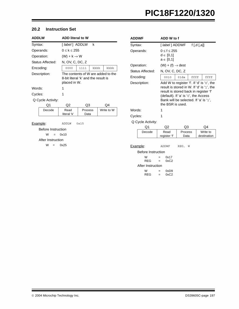
PIC18F1220/1320
20.2 Instruction Set
ADDLW ADD literal to W
Syntax: [ label ] ADDLW k
Operands: 0 ≤ k ≤ 255
Operation: (W) + k → W
Status Affected: N, OV, C, DC, Z
Encoding: 0000 1111 kkkk kkkk
Description: The contents of W are added to the 8-bit literal ‘k’ and the result is placed in W.
Words: 1
Cycles: 1
Q Cycle Activity:Q1 Q2 Q3 Q4
Decode Readliteral ‘k’
Process Data
Write to W
Example: ADDLW 0x15
Before InstructionW = 0x10
After InstructionW = 0x25
ADDWF ADD W to f
Syntax: [ label ] ADDWF f [,d [,a]]
Operands: 0 ≤ f ≤ 255d ∈ [0,1]a ∈ [0,1]
Operation: (W) + (f) → dest
Status Affected: N, OV, C, DC, Z
Encoding: 0010 01da ffff ffff
Description: Add W to register ‘f’. If ‘d’ is ‘0’, the result is stored in W. If ‘d’ is ‘1’, the result is stored back in register ‘f’ (default). If ‘a’ is ‘0’, the Access Bank will be selected. If ‘a’ is ‘1’, the BSR is used.
Words: 1
Cycles: 1
Q Cycle Activity:
Q1 Q2 Q3 Q4Decode Read
register ‘f’Process
DataWrite to
destination
Example: ADDWF REG, W
Before InstructionW = 0x17REG = 0xC2
After InstructionW = 0xD9REG = 0xC2
2004 Microchip Technology Inc. DS39605C-page 197
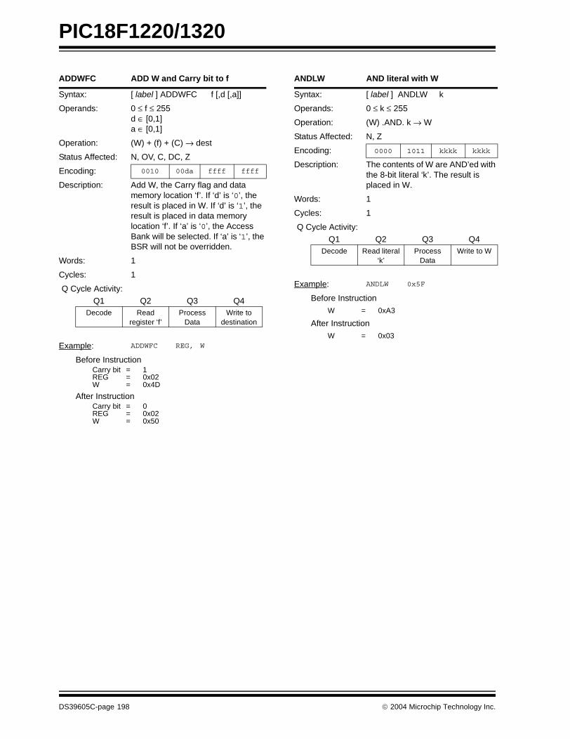
PIC18F1220/1320
ADDWFC ADD W and Carry bit to f
Syntax: [ label ] ADDWFC f [,d [,a]]
Operands: 0 ≤ f ≤ 255d ∈ [0,1]a ∈ [0,1]
Operation: (W) + (f) + (C) → dest
Status Affected: N, OV, C, DC, Z
Encoding: 0010 00da ffff ffff
Description: Add W, the Carry flag and data memory location ‘f’. If ‘d’ is ‘0’, the result is placed in W. If ‘d’ is ‘1’, the result is placed in data memory location ‘f’. If ‘a’ is ‘0’, the Access Bank will be selected. If ‘a’ is ‘1’, the BSR will not be overridden.
Words: 1
Cycles: 1
Q Cycle Activity:
Q1 Q2 Q3 Q4Decode Read
register ‘f’Process
DataWrite to
destination
Example: ADDWFC REG, W
Before InstructionCarry bit = 1REG = 0x02W = 0x4D
After InstructionCarry bit = 0REG = 0x02W = 0x50
ANDLW AND literal with W
Syntax: [ label ] ANDLW k
Operands: 0 ≤ k ≤ 255
Operation: (W) .AND. k → W
Status Affected: N, Z
Encoding: 0000 1011 kkkk kkkk
Description: The contents of W are AND’ed with the 8-bit literal ‘k’. The result is placed in W.
Words: 1
Cycles: 1
Q Cycle Activity:
Q1 Q2 Q3 Q4Decode Read literal
‘k’Process
DataWrite to W
Example: ANDLW 0x5F
Before InstructionW = 0xA3
After InstructionW = 0x03
DS39605C-page 198 2004 Microchip Technology Inc.
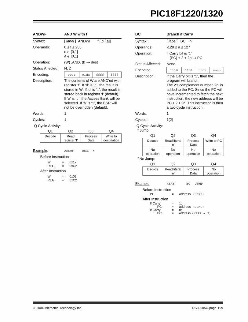
PIC18F1220/1320
ANDWF AND W with f
Syntax: [ label ] ANDWF f [,d [,a]]
Operands: 0 ≤ f ≤ 255d ∈ [0,1]a ∈ [0,1]
Operation: (W) .AND. (f) → dest
Status Affected: N, Z
Encoding: 0001 01da ffff ffff
Description: The contents of W are AND’ed with register ‘f’. If ‘d’ is ‘0’, the result is stored in W. If ‘d’ is ‘1’, the result is stored back in register ‘f’ (default). If ‘a’ is ‘0’, the Access Bank will be selected. If ‘a’ is ‘1’, the BSR will not be overridden (default).
Words: 1
Cycles: 1
Q Cycle Activity:
Q1 Q2 Q3 Q4Decode Read
register ‘f’Process
DataWrite to
destination
Example: ANDWF REG, W
Before InstructionW = 0x17REG = 0xC2
After Instruction
W = 0x02REG = 0xC2
BC Branch if Carry
Syntax: [ label ] BC n
Operands: -128 ≤ n ≤ 127
Operation: if Carry bit is ‘1’ (PC) + 2 + 2n → PC
Status Affected: None
Encoding: 1110 0010 nnnn nnnn
Description: If the Carry bit is ‘1’, then the program will branch.The 2’s complement number ‘2n’ is added to the PC. Since the PC will have incremented to fetch the next instruction, the new address will be PC + 2 + 2n. This instruction is then a two-cycle instruction.
Words: 1
Cycles: 1(2)
Q Cycle Activity:If Jump:
Q1 Q2 Q3 Q4Decode Read literal
‘n’Process
DataWrite to PC
No operation
No operation
No operation
No operation
If No Jump:
Q1 Q2 Q3 Q4Decode Read literal
‘n’Process
DataNo
operation
Example: HERE BC JUMP
Before InstructionPC = address (HERE)
After InstructionIf Carry = 1;
PC = address (JUMP)If Carry = 0;
PC = address (HERE + 2)
2004 Microchip Technology Inc. DS39605C-page 199
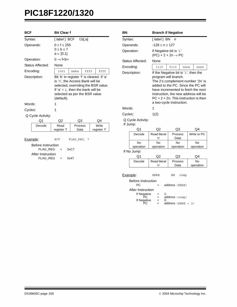
PIC18F1220/1320
BCF Bit Clear f
Syntax: [ label ] BCF f,b[,a]
Operands: 0 ≤ f ≤ 2550 ≤ b ≤ 7a ∈ [0,1]
Operation: 0 → f<b>
Status Affected: None
Encoding: 1001 bbba ffff ffff
Description: Bit ‘b’ in register ‘f’ is cleared. If ‘a’ is ‘0’, the Access Bank will be selected, overriding the BSR value. If ‘a’ = 1, then the bank will be selected as per the BSR value (default).
Words: 1
Cycles: 1
Q Cycle Activity:Q1 Q2 Q3 Q4
Decode Readregister ‘f’
Process Data
Writeregister ‘f’
Example: BCF FLAG_REG, 7
Before InstructionFLAG_REG = 0xC7
After InstructionFLAG_REG = 0x47
BN Branch if Negative
Syntax: [ label ] BN n
Operands: -128 ≤ n ≤ 127
Operation: if Negative bit is ‘1’(PC) + 2 + 2n → PC
Status Affected: None
Encoding: 1110 0110 nnnn nnnn
Description: If the Negative bit is ‘1’, then the program will branch.The 2’s complement number ‘2n’ is added to the PC. Since the PC will have incremented to fetch the next instruction, the new address will be PC + 2 + 2n. This instruction is then a two-cycle instruction.
Words: 1
Cycles: 1(2)
Q Cycle Activity:If Jump:
Q1 Q2 Q3 Q4Decode Read literal
‘n’Process
DataWrite to PC
No operation
No operation
No operation
No operation
If No Jump:
Q1 Q2 Q3 Q4Decode Read literal
‘n’Process
DataNo
operation
Example: HERE BN Jump
Before InstructionPC = address (HERE)
After InstructionIf Negative = 1;
PC = address (Jump)If Negative = 0;
PC = address (HERE + 2)
DS39605C-page 200 2004 Microchip Technology Inc.
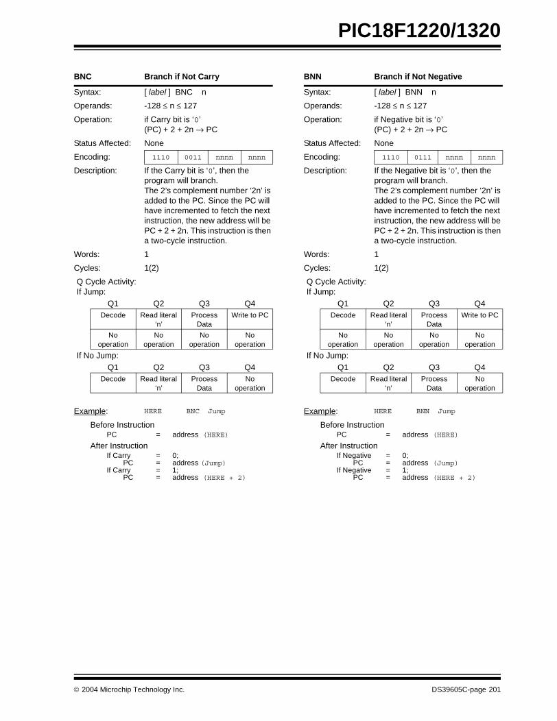
PIC18F1220/1320
BNC Branch if Not Carry
Syntax: [ label ] BNC n
Operands: -128 ≤ n ≤ 127
Operation: if Carry bit is ‘0’(PC) + 2 + 2n → PC
Status Affected: None
Encoding: 1110 0011 nnnn nnnn
Description: If the Carry bit is ‘0’, then the program will branch.The 2’s complement number ‘2n’ is added to the PC. Since the PC will have incremented to fetch the next instruction, the new address will be PC + 2 + 2n. This instruction is then a two-cycle instruction.
Words: 1
Cycles: 1(2)
Q Cycle Activity:If Jump:
Q1 Q2 Q3 Q4Decode Read literal
‘n’Process
DataWrite to PC
No operation
No operation
No operation
No operation
If No Jump:
Q1 Q2 Q3 Q4Decode Read literal
‘n’Process
DataNo
operation
Example: HERE BNC Jump
Before InstructionPC = address (HERE)
After InstructionIf Carry = 0;
PC = address (Jump)If Carry = 1;
PC = address (HERE + 2)
BNN Branch if Not Negative
Syntax: [ label ] BNN n
Operands: -128 ≤ n ≤ 127
Operation: if Negative bit is ‘0’(PC) + 2 + 2n → PC
Status Affected: None
Encoding: 1110 0111 nnnn nnnn
Description: If the Negative bit is ‘0’, then the program will branch.The 2’s complement number ‘2n’ is added to the PC. Since the PC will have incremented to fetch the next instruction, the new address will be PC + 2 + 2n. This instruction is then a two-cycle instruction.
Words: 1
Cycles: 1(2)
Q Cycle Activity:If Jump:
Q1 Q2 Q3 Q4Decode Read literal
‘n’Process
DataWrite to PC
No operation
No operation
No operation
No operation
If No Jump:
Q1 Q2 Q3 Q4Decode Read literal
‘n’Process
DataNo
operation
Example: HERE BNN Jump
Before InstructionPC = address (HERE)
After InstructionIf Negative = 0;
PC = address (Jump)If Negative = 1;
PC = address (HERE + 2)
2004 Microchip Technology Inc. DS39605C-page 201
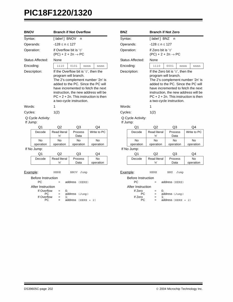
PIC18F1220/1320
BNOV Branch if Not Overflow
Syntax: [ label ] BNOV n
Operands: -128 ≤ n ≤ 127
Operation: if Overflow bit is ‘0’(PC) + 2 + 2n → PC
Status Affected: None
Encoding: 1110 0101 nnnn nnnn
Description: If the Overflow bit is ‘0’, then the program will branch.The 2’s complement number ‘2n’ is added to the PC. Since the PC will have incremented to fetch the next instruction, the new address will be PC + 2 + 2n. This instruction is then a two-cycle instruction.
Words: 1
Cycles: 1(2)
Q Cycle Activity:If Jump:
Q1 Q2 Q3 Q4Decode Read literal
‘n’Process
DataWrite to PC
No operation
No operation
No operation
No operation
If No Jump:
Q1 Q2 Q3 Q4Decode Read literal
‘n’Process
DataNo
operation
Example: HERE BNOV Jump
Before InstructionPC = address (HERE)
After InstructionIf Overflow = 0;
PC = address (Jump)If Overflow = 1;
PC = address (HERE + 2)
BNZ Branch if Not Zero
Syntax: [ label ] BNZ n
Operands: -128 ≤ n ≤ 127
Operation: if Zero bit is ‘0’(PC) + 2 + 2n → PC
Status Affected: None
Encoding: 1110 0001 nnnn nnnn
Description: If the Zero bit is ‘0’, then the program will branch.The 2’s complement number ‘2n’ is added to the PC. Since the PC will have incremented to fetch the next instruction, the new address will be PC + 2 + 2n. This instruction is then a two-cycle instruction.
Words: 1
Cycles: 1(2)
Q Cycle Activity:If Jump:
Q1 Q2 Q3 Q4Decode Read literal
‘n’Process
DataWrite to PC
No operation
No operation
No operation
No operation
If No Jump:
Q1 Q2 Q3 Q4Decode Read literal
‘n’Process
DataNo
operation
Example: HERE BNZ Jump
Before InstructionPC = address (HERE)
After InstructionIf Zero = 0;
PC = address (Jump)If Zero = 1;
PC = address (HERE + 2)
DS39605C-page 202 2004 Microchip Technology Inc.
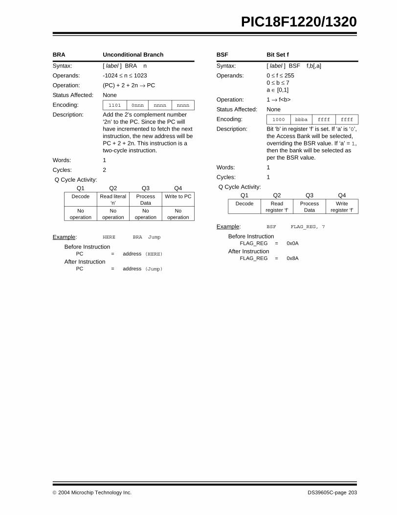
PIC18F1220/1320
BRA Unconditional Branch
Syntax: [ label ] BRA n
Operands: -1024 ≤ n ≤ 1023
Operation: (PC) + 2 + 2n → PC
Status Affected: None
Encoding: 1101 0nnn nnnn nnnn
Description: Add the 2’s complement number ‘2n’ to the PC. Since the PC will have incremented to fetch the next instruction, the new address will be PC + 2 + 2n. This instruction is a two-cycle instruction.
Words: 1
Cycles: 2
Q Cycle Activity:
Q1 Q2 Q3 Q4Decode Read literal
‘n’Process
DataWrite to PC
No operation
No operation
No operation
No operation
Example: HERE BRA Jump
Before InstructionPC = address (HERE)
After InstructionPC = address (Jump)
BSF Bit Set f
Syntax: [ label ] BSF f,b[,a]
Operands: 0 ≤ f ≤ 2550 ≤ b ≤ 7a ∈ [0,1]
Operation: 1 → f<b>
Status Affected: None
Encoding: 1000 bbba ffff ffff
Description: Bit ‘b’ in register ‘f’ is set. If ‘a’ is ‘0’, the Access Bank will be selected, overriding the BSR value. If ‘a’ = 1, then the bank will be selected as per the BSR value.
Words: 1
Cycles: 1
Q Cycle Activity:Q1 Q2 Q3 Q4
Decode Readregister ‘f’
Process Data
Writeregister ‘f’
Example: BSF FLAG_REG, 7
Before InstructionFLAG_REG = 0x0A
After InstructionFLAG_REG = 0x8A
2004 Microchip Technology Inc. DS39605C-page 203
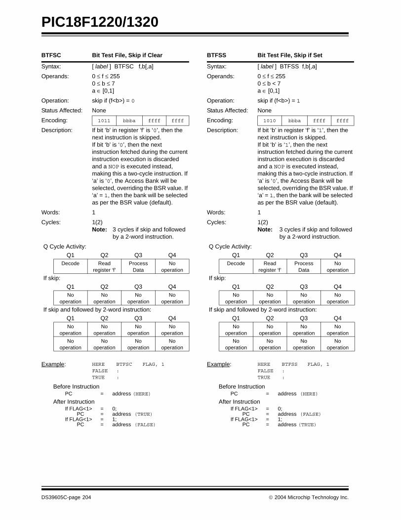
PIC18F1220/1320
BTFSC Bit Test File, Skip if Clear
Syntax: [ label ] BTFSC f,b[,a]
Operands: 0 ≤ f ≤ 2550 ≤ b ≤ 7a ∈ [0,1]
Operation: skip if (f<b>) = 0
Status Affected: None
Encoding: 1011 bbba ffff ffff
Description: If bit ‘b’ in register ‘f’ is ‘0’, then the next instruction is skipped.If bit ‘b’ is ‘0’, then the next instruction fetched during the current instruction execution is discarded and a NOP is executed instead, making this a two-cycle instruction. If ‘a’ is ‘0’, the Access Bank will be selected, overriding the BSR value. If ‘a’ = 1, then the bank will be selected as per the BSR value (default).
Words: 1
Cycles: 1(2)Note: 3 cycles if skip and followed
by a 2-word instruction.
Q Cycle Activity:
Q1 Q2 Q3 Q4Decode Read
register ‘f’Process
DataNo
operation
If skip:
Q1 Q2 Q3 Q4No
operationNo
operationNo
operationNo
operation
If skip and followed by 2-word instruction:
Q1 Q2 Q3 Q4No
operationNo
operationNo
operationNo
operation
No operation
No operation
No operation
No operation
Example: HEREFALSETRUE
BTFSC::
FLAG, 1
Before InstructionPC = address (HERE)
After InstructionIf FLAG<1> = 0;
PC = address (TRUE)If FLAG<1> = 1;
PC = address (FALSE)
BTFSS Bit Test File, Skip if Set
Syntax: [ label ] BTFSS f,b[,a]
Operands: 0 ≤ f ≤ 2550 ≤ b < 7a ∈ [0,1]
Operation: skip if (f<b>) = 1
Status Affected: None
Encoding: 1010 bbba ffff ffff
Description: If bit ‘b’ in register ‘f’ is ‘1’, then the next instruction is skipped.If bit ‘b’ is ‘1’, then the next instruction fetched during the current instruction execution is discarded and a NOP is executed instead, making this a two-cycle instruction. If ‘a’ is ‘0’, the Access Bank will be selected, overriding the BSR value. If ‘a’ = 1, then the bank will be selected as per the BSR value (default).
Words: 1
Cycles: 1(2)Note: 3 cycles if skip and followed
by a 2-word instruction.
Q Cycle Activity:
Q1 Q2 Q3 Q4Decode Read
register ‘f’Process
DataNo
operation
If skip:
Q1 Q2 Q3 Q4No
operationNo
operationNo
operationNo
operation
If skip and followed by 2-word instruction:
Q1 Q2 Q3 Q4No
operationNo
operationNo
operationNo
operation
No operation
No operation
No operation
No operation
Example: HEREFALSETRUE
BTFSS::
FLAG, 1
Before InstructionPC = address (HERE)
After InstructionIf FLAG<1> = 0;
PC = address (FALSE)If FLAG<1> = 1;
PC = address (TRUE)
DS39605C-page 204 2004 Microchip Technology Inc.
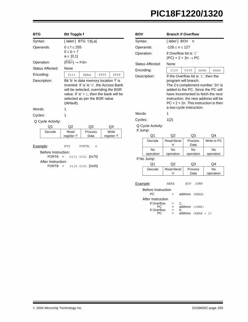
PIC18F1220/1320
BTG Bit Toggle f
Syntax: [ label ] BTG f,b[,a]
Operands: 0 ≤ f ≤ 2550 ≤ b < 7a ∈ [0,1]
Operation: (f<b>) → f<b>
Status Affected: None
Encoding: 0111 bbba ffff ffff
Description: Bit ‘b’ in data memory location ‘f’ is inverted. If ‘a’ is ‘0’, the Access Bank will be selected, overriding the BSR value. If ‘a’ = 1, then the bank will be selected as per the BSR value (default).
Words: 1
Cycles: 1
Q Cycle Activity:Q1 Q2 Q3 Q4
Decode Readregister ‘f’
Process Data
Writeregister ‘f’
Example: BTG PORTB, 4
Before Instruction:PORTB = 0111 0101 [0x75]
After Instruction:PORTB = 0110 0101 [0x65]
BOV Branch if Overflow
Syntax: [ label ] BOV n
Operands: -128 ≤ n ≤ 127
Operation: if Overflow bit is ‘1’(PC) + 2 + 2n → PC
Status Affected: None
Encoding: 1110 0100 nnnn nnnn
Description: If the Overflow bit is ‘1’, then the program will branch.The 2’s complement number ‘2n’ is added to the PC. Since the PC will have incremented to fetch the next instruction, the new address will be PC + 2 + 2n. This instruction is then a two-cycle instruction.
Words: 1
Cycles: 1(2)
Q Cycle Activity:If Jump:
Q1 Q2 Q3 Q4Decode Read literal
‘n’Process
DataWrite to PC
No operation
No operation
No operation
No operation
If No Jump:
Q1 Q2 Q3 Q4Decode Read literal
‘n’Process
DataNo
operation
Example: HERE BOV JUMP
Before InstructionPC = address (HERE)
After InstructionIf Overflow = 1;
PC = address (JUMP)If Overflow = 0;
PC = address (HERE + 2)
2004 Microchip Technology Inc. DS39605C-page 205

PIC18F1220/1320
BZ Branch if Zero
Syntax: [ label ] BZ n
Operands: -128 ≤ n ≤ 127
Operation: if Zero bit is ‘1’(PC) + 2 + 2n → PC
Status Affected: None
Encoding: 1110 0000 nnnn nnnn
Description: If the Zero bit is ‘1’, then the program will branch.The 2’s complement number ‘2n’ is added to the PC. Since the PC will have incremented to fetch the next instruction, the new address will be PC + 2 + 2n. This instruction is then a two-cycle instruction.
Words: 1
Cycles: 1(2)
Q Cycle Activity:If Jump:
Q1 Q2 Q3 Q4Decode Read literal
‘n’Process
DataWrite to PC
No operation
No operation
No operation
No operation
If No Jump:
Q1 Q2 Q3 Q4Decode Read literal
‘n’Process
DataNo
operation
Example: HERE BZ Jump
Before InstructionPC = address (HERE)
After InstructionIf Zero = 1;
PC = address (Jump)If Zero = 0;
PC = address (HERE + 2)
CALL Subroutine Call
Syntax: [ label ] CALL k [,s]
Operands: 0 ≤ k ≤ 1048575s ∈ [0,1]
Operation: (PC) + 4 → TOS,k → PC<20:1>,if s = 1(W) → WS,(Status) → STATUSS,(BSR) → BSRS
Status Affected: None
Encoding:1st word (k<7:0>)2nd word(k<19:8>)
11101111
110sk19kkk
k7kkkkkkk
kkkk0kkkk8
Description: Subroutine call of entire 2-Mbyte memory range. First, return address (PC + 4) is pushed onto the return stack. If ‘s’ = 1, the W, Status and BSR registers are also pushed into their respective shadow registers, WS, STATUSS and BSRS. If ‘s’ = 0, no update occurs (default). Then, the 20-bit value ‘k’ is loaded into PC<20:1>. CALL is a two-cycle instruction.
Words: 2
Cycles: 2
Q Cycle Activity:Q1 Q2 Q3 Q4
Decode Read literal ‘k’<7:0>,
Push PC to stack
Read literal ‘k’<19:8>,
Write to PC
No operation
No operation
No operation
No operation
Example: HERE CALL THERE, FAST
Before InstructionPC = address (HERE)
After InstructionPC = address (THERE)TOS = address (HERE + 4)WS = WBSRS = BSRSTATUSS = Status
DS39605C-page 206 2004 Microchip Technology Inc.
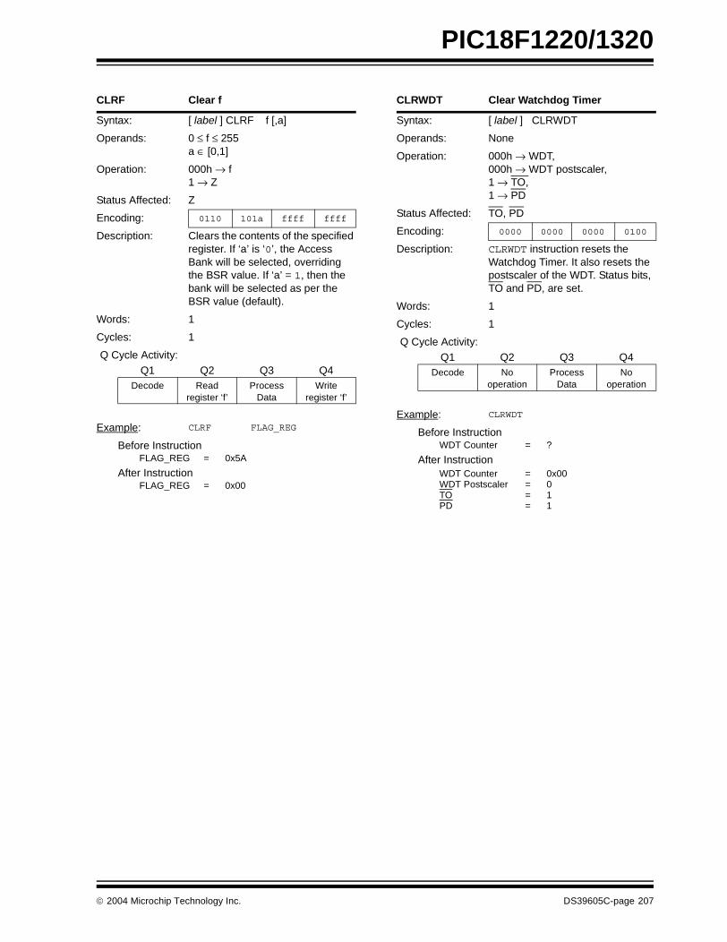
PIC18F1220/1320
CLRF Clear f
Syntax: [ label ] CLRF f [,a]
Operands: 0 ≤ f ≤ 255a ∈ [0,1]
Operation: 000h → f1 → Z
Status Affected: Z
Encoding: 0110 101a ffff ffff
Description: Clears the contents of the specified register. If ‘a’ is ‘0’, the Access Bank will be selected, overriding the BSR value. If ‘a’ = 1, then the bank will be selected as per the BSR value (default).
Words: 1
Cycles: 1
Q Cycle Activity:Q1 Q2 Q3 Q4
Decode Readregister ‘f’
Process Data
Writeregister ‘f’
Example: CLRF FLAG_REG
Before InstructionFLAG_REG = 0x5A
After InstructionFLAG_REG = 0x00
CLRWDT Clear Watchdog Timer
Syntax: [ label ] CLRWDT
Operands: None
Operation: 000h → WDT,000h → WDT postscaler,1 → TO,1 → PD
Status Affected: TO, PD
Encoding: 0000 0000 0000 0100
Description: CLRWDT instruction resets the Watchdog Timer. It also resets the postscaler of the WDT. Status bits, TO and PD, are set.
Words: 1
Cycles: 1
Q Cycle Activity:Q1 Q2 Q3 Q4
Decode No operation
Process Data
No operation
Example: CLRWDT
Before InstructionWDT Counter = ?
After InstructionWDT Counter = 0x00WDT Postscaler = 0TO = 1PD = 1
2004 Microchip Technology Inc. DS39605C-page 207

PIC18F1220/1320
COMF Complement f
Syntax: [ label ] COMF f [,d [,a]]
Operands: 0 ≤ f ≤ 255d ∈ [0,1]a ∈ [0,1]
Operation: (f) → dest
Status Affected: N, Z
Encoding: 0001 11da ffff ffff
Description: The contents of register ‘f’ are complemented. If ‘d’ is ‘0’, the result is stored in W. If ‘d’ is ‘1’, the result is stored back in register ‘f’ (default). If ‘a’ is ‘0’, the Access Bank will be selected, overriding the BSR value. If ‘a’ = 1, then the bank will be selected as per the BSR value (default).
Words: 1
Cycles: 1
Q Cycle Activity:Q1 Q2 Q3 Q4
Decode Readregister ‘f’
Process Data
Write todestination
Example: COMF REG, W
Before InstructionREG = 0x13
After InstructionREG = 0x13W = 0xEC
CPFSEQ Compare f with W, skip if f = W
Syntax: [ label ] CPFSEQ f [,a]
Operands: 0 ≤ f ≤ 255a ∈ [0,1]
Operation: (f) – (W), skip if (f) = (W) (unsigned comparison)
Status Affected: None
Encoding: 0110 001a ffff ffff
Description: Compares the contents of data memory location ‘f’ to the contents of W by performing an unsigned subtraction.If ‘f’ = W, then the fetched instruction is discarded and a NOP is executed instead, making this a two-cycle instruction. If ‘a’ is ‘0’, the Access Bank will be selected, overriding the BSR value. If ‘a’ = 1, then the bank will be selected as per the BSR value (default).
Words: 1
Cycles: 1(2)Note: 3 cycles if skip and followed
by a 2-word instruction.
Q Cycle Activity:Q1 Q2 Q3 Q4
Decode Readregister ‘f’
Process Data
No operation
If skip:Q1 Q2 Q3 Q4No
operationNo
operationNo
operationNo
operation
If skip and followed by 2-word instruction:Q1 Q2 Q3 Q4No
operationNo
operationNo
operationNo
operation
No operation
No operation
No operation
No operation
Example: HERE CPFSEQ REGNEQUAL :EQUAL :
Before InstructionPC Address = HEREW = ?REG = ?
After InstructionIf REG = W;
PC = Address (EQUAL)If REG ≠ W;
PC = Address (NEQUAL)
DS39605C-page 208 2004 Microchip Technology Inc.

PIC18F1220/1320
CPFSGT Compare f with W, skip if f > W
Syntax: [ label ] CPFSGT f [,a]
Operands: 0 ≤ f ≤ 255a ∈ [0,1]
Operation: (f) – (W),skip if (f) > (W) (unsigned comparison)
Status Affected: None
Encoding: 0110 010a ffff ffff
Description: Compares the contents of data memory location ‘f’ to the contents of W by performing an unsigned subtraction.If the contents of ‘f’ are greater than the contents of WREG, then the fetched instruction is discarded and a NOP is executed instead, making this a two-cycle instruction. If ‘a’ is ‘0’, the Access Bank will be selected, overriding the BSR value. If ‘a’ = 1, then the bank will be selected as per the BSR value (default).
Words: 1
Cycles: 1(2)Note: 3 cycles if skip and followed
by a 2-word instruction.
Q Cycle Activity:Q1 Q2 Q3 Q4
Decode Readregister ‘f’
Process Data
No operation
If skip:Q1 Q2 Q3 Q4No
operationNo
operationNo
operationNo
operation
If skip and followed by 2-word instruction:Q1 Q2 Q3 Q4No
operationNo
operationNo
operationNo
operation
No operation
No operation
No operation
No operation
Example: HERE CPFSGT REGNGREATER :GREATER :
Before InstructionPC = Address (HERE)W = ?
After InstructionIf REG > W;
PC = Address (GREATER)If REG ≤ W;
PC = Address (NGREATER)
CPFSLT Compare f with W, skip if f < W
Syntax: [ label ] CPFSLT f [,a]
Operands: 0 ≤ f ≤ 255a ∈ [0,1]
Operation: (f) – (W),skip if (f) < (W) (unsigned comparison)
Status Affected: None
Encoding: 0110 000a ffff ffff
Description: Compares the contents of data memory location ‘f’ to the contents of W by performing an unsigned subtraction.If the contents of ‘f’ are less than the contents of W, then the fetched instruction is discarded and a NOP is executed instead, making this a two-cycle instruction. If ‘a’ is ‘0’, the Access Bank will be selected. If ‘a’ is ‘1’, the BSR will not be overridden (default).
Words: 1
Cycles: 1(2)Note: 3 cycles if skip and followed
by a 2-word instruction.
Q Cycle Activity:Q1 Q2 Q3 Q4
Decode Readregister ‘f’
Process Data
No operation
If skip:Q1 Q2 Q3 Q4No
operationNo
operationNo
operationNo
operation
If skip and followed by 2-word instruction:Q1 Q2 Q3 Q4No
operationNo
operationNo
operationNo
operation
No operation
No operation
No operation
No operation
Example: HERE CPFSLT REGNLESS :LESS :
Before InstructionPC = Address (HERE)W = ?
After InstructionIf REG < W;
PC = Address (LESS)If REG ≥ W;
PC = Address (NLESS)
2004 Microchip Technology Inc. DS39605C-page 209
PIC18F1220/1320
DAW Decimal Adjust W Register
Syntax: [ label ] DAW
Operands: None
Operation: If [W<3:0> > 9] or [DC = 1] then(W<3:0>) + 6 → W<3:0>;else (W<3:0>) → W<3:0>;
If [W<7:4> > 9] or [C = 1] then(W<7:4>) + 6 → W<7:4>;else (W<7:4>) → W<7:4>;
Status Affected: C, DC
Encoding: 0000 0000 0000 0111
Description: DAW adjusts the eight-bit value in W, resulting from the earlier addi-tion of two variables (each in packed BCD format) and produces a correct packed BCD result. The Carry bit may be set by DAW regard-less of its setting prior to the DAW instruction.
Words: 1
Cycles: 1
Q Cycle Activity:Q1 Q2 Q3 Q4
Decode Readregister W
Process Data
WriteW
Example 1: DAW
Before InstructionW = 0xA5C = 0DC = 0
After InstructionW = 0x05C = 1DC = 0
Example 2:
Before InstructionW = 0xCEC = 0DC = 0
After InstructionW = 0x34C = 1DC = 0
DECF Decrement f
Syntax: [ label ] DECF f [,d [,a]]
Operands: 0 ≤ f ≤ 255d ∈ [0,1]a ∈ [0,1]
Operation: (f) – 1 → dest
Status Affected: C, DC, N, OV, Z
Encoding: 0000 01da ffff ffff
Description: Decrement register ‘f’. If ‘d’ is ‘0’, the result is stored in W. If ‘d’ is ‘1’, the result is stored back in register ‘f’ (default). If ‘a’ is ‘0’, the Access Bank will be selected, overriding the BSR value. If ‘a’ = 1, then the bank will be selected as per the BSR value (default).
Words: 1
Cycles: 1
Q Cycle Activity:Q1 Q2 Q3 Q4
Decode Readregister ‘f’
Process Data
Write to destination
Example: DECF CNT
Before InstructionCNT = 0x01Z = 0
After InstructionCNT = 0x00Z = 1
DS39605C-page 210 2004 Microchip Technology Inc.

PIC18F1220/1320
DECFSZ Decrement f, skip if 0
Syntax: [ label ] DECFSZ f [,d [,a]]
Operands: 0 ≤ f ≤ 255d ∈ [0,1]a ∈ [0,1]
Operation: (f) – 1 → dest,skip if result = 0
Status Affected: None
Encoding: 0010 11da ffff ffff
Description: The contents of register ‘f’ are decremented. If ‘d’ is ‘0’, the result is placed in W. If ‘d’ is ‘1’, the result is placed back in register ‘f’ (default).If the result is ‘0’, the next instruc-tion, which is already fetched, is discarded and a NOP is executed instead, making it a two-cycle instruction. If ‘a’ is ‘0’, the Access Bank will be selected, overriding the BSR value. If ‘a’ = 1, then the bank will be selected as per the BSR value (default).
Words: 1
Cycles: 1(2)Note: 3 cycles if skip and followed
by a 2-word instruction.
Q Cycle Activity:Q1 Q2 Q3 Q4
Decode Readregister ‘f’
Process Data
Write to destination
If skip:Q1 Q2 Q3 Q4No
operationNo
operationNo
operationNo
operation
If skip and followed by 2-word instruction:Q1 Q2 Q3 Q4No
operationNo
operationNo
operationNo
operation
No operation
No operation
No operation
No operation
Example: HERE DECFSZ CNT GOTO LOOPCONTINUE
Before InstructionPC = Address (HERE)
After InstructionCNT = CNT – 1If CNT = 0;
PC = Address (CONTINUE)If CNT ≠ 0;
PC = Address (HERE + 2)
DCFSNZ Decrement f, skip if not 0
Syntax: [ label ] DCFSNZ f [,d [,a]]
Operands: 0 ≤ f ≤ 255d ∈ [0,1]a ∈ [0,1]
Operation: (f) – 1 → dest,skip if result ≠ 0
Status Affected: None
Encoding: 0100 11da ffff ffff
Description: The contents of register ‘f’ are decremented. If ‘d’ is ‘0’, the result is placed in W. If ‘d’ is ‘1’, the result is placed back in register ‘f’ (default).If the result is not ‘0’, the next instruction, which is already fetched, is discarded and a NOP is executed instead, making it a two-cycle instruction. If ‘a’ is ‘0’, the Access Bank will be selected, overriding the BSR value. If ‘a’ = 1, then the bank will be selected as per the BSR value (default).
Words: 1
Cycles: 1(2)Note: 3 cycles if skip and followed
by a 2-word instruction.
Q Cycle Activity:Q1 Q2 Q3 Q4
Decode Readregister ‘f’
Process Data
Write to destination
If skip:Q1 Q2 Q3 Q4No
operationNo
operationNo
operationNo
operation
If skip and followed by 2-word instruction:Q1 Q2 Q3 Q4No
operationNo
operationNo
operationNo
operation
No operation
No operation
No operation
No operation
Example: HERE DCFSNZ TEMPZERO : NZERO :
Before InstructionTEMP = ?
After InstructionTEMP = TEMP – 1,If TEMP = 0;
PC = Address (ZERO)If TEMP ≠ 0;
PC = Address (NZERO)
2004 Microchip Technology Inc. DS39605C-page 211

PIC18F1220/1320
GOTO Unconditional Branch
Syntax: [ label ] GOTO k
Operands: 0 ≤ k ≤ 1048575
Operation: k → PC<20:1>
Status Affected: None
Encoding:1st word (k<7:0>)2nd word(k<19:8>)
11101111
1111k19kkk
k7kkkkkkk
kkkk0kkkk8
Description: GOTO allows an unconditional branch anywhere within the entire 2-Mbyte memory range. The 20-bit value ‘k’ is loaded into PC<20:1>. GOTO is always a two-cycle instruction.
Words: 2
Cycles: 2
Q Cycle Activity:Q1 Q2 Q3 Q4
Decode Read literal ‘k’<7:0>,
No operation
Read literal ‘k’<19:8>,
Write to PC
No operation
No operation
No operation
No operation
Example: GOTO THERE
After InstructionPC = Address (THERE)
INCF Increment f
Syntax: [ label ] INCF f [,d [,a]]
Operands: 0 ≤ f ≤ 255d ∈ [0,1]a ∈ [0,1]
Operation: (f) + 1 → dest
Status Affected: C, DC, N, OV, Z
Encoding: 0010 10da ffff ffff
Description: The contents of register ‘f’ are incremented. If ‘d’ is ‘0’, the result is placed in W. If ‘d’ is ‘1’, the result is placed back in register ‘f’ (default). If ‘a’ is ‘0’, the Access Bank will be selected, overriding the BSR value. If ‘a’ = 1, then the bank will be selected as per the BSR value (default).
Words: 1
Cycles: 1
Q Cycle Activity:Q1 Q2 Q3 Q4
Decode Readregister ‘f’
Process Data
Write to destination
Example: INCF CNT
Before InstructionCNT = 0xFFZ = 0C = ?DC = ?
After InstructionCNT = 0x00Z = 1C = 1DC = 1
DS39605C-page 212 2004 Microchip Technology Inc.

PIC18F1220/1320
INCFSZ Increment f, skip if 0
Syntax: [ label ] INCFSZ f [,d [,a]]
Operands: 0 ≤ f ≤ 255d ∈ [0,1]a ∈ [0,1]
Operation: (f) + 1 → dest,skip if result = 0
Status Affected: None
Encoding: 0011 11da ffff ffff
Description: The contents of register ‘f’ are incremented. If ‘d’ is ‘0’, the result is placed in W. If ‘d’ is ‘1’, the result is placed back in register ‘f’ (default).If the result is ‘0’, the next instruc-tion, which is already fetched, is discarded and a NOP is executed instead, making it a two-cycle instruction. If ‘a’ is ‘0’, the Access Bank will be selected, overriding the BSR value. If ‘a’ = 1, then the bank will be selected as per the BSR value (default).
Words: 1
Cycles: 1(2)Note: 3 cycles if skip and followed
by a 2-word instruction.
Q Cycle Activity:Q1 Q2 Q3 Q4
Decode Readregister ‘f’
Process Data
Write to destination
If skip:Q1 Q2 Q3 Q4No
operationNo
operationNo
operationNo
operation
If skip and followed by 2-word instruction:Q1 Q2 Q3 Q4No
operationNo
operationNo
operationNo
operation
No operation
No operation
No operation
No operation
Example: HERE INCFSZ CNTNZERO : ZERO :
Before InstructionPC = Address (HERE)
After InstructionCNT = CNT + 1If CNT = 0;PC = Address (ZERO)If CNT ≠ 0;PC = Address (NZERO)
INFSNZ Increment f, skip if not 0
Syntax: [ label ] INFSNZ f [,d [,a]]
Operands: 0 ≤ f ≤ 255d ∈ [0,1]a ∈ [0,1]
Operation: (f) + 1 → dest, skip if result ≠ 0
Status Affected: None
Encoding: 0100 10da ffff ffff
Description: The contents of register ‘f’ are incremented. If ‘d’ is ‘0’, the result is placed in W. If ‘d’ is ‘1’, the result is placed back in register ‘f’ (default).If the result is not ‘0’, the next instruction, which is already fetched, is discarded and a NOP is executed instead, making it a two-cycle instruction. If ‘a’ is ‘0’, the Access Bank will be selected, over-riding the BSR value. If ‘a’ = 1, then the bank will be selected as per the BSR value (default).
Words: 1
Cycles: 1(2)Note: 3 cycles if skip and followed
by a 2-word instruction.
Q Cycle Activity:Q1 Q2 Q3 Q4
Decode Readregister ‘f’
Process Data
Write to destination
If skip:Q1 Q2 Q3 Q4No
operationNo
operationNo
operationNo
operation
If skip and followed by 2-word instruction:Q1 Q2 Q3 Q4No
operationNo
operationNo
operationNo
operation
No operation
No operation
No operation
No operation
Example: HERE INFSNZ REGZERONZERO
Before InstructionPC = Address (HERE)
After InstructionREG = REG + 1If REG ≠ 0;PC = Address (NZERO)If REG = 0;PC = Address (ZERO)
2004 Microchip Technology Inc. DS39605C-page 213
PIC18F1220/1320
IORLW Inclusive OR literal with W
Syntax: [ label ] IORLW k
Operands: 0 ≤ k ≤ 255
Operation: (W) .OR. k → W
Status Affected: N, Z
Encoding: 0000 1001 kkkk kkkk
Description: The contents of W are OR’ed with the eight-bit literal ‘k’. The result is placed in W.
Words: 1
Cycles: 1
Q Cycle Activity:
Q1 Q2 Q3 Q4Decode Read
literal ‘k’Process
DataWrite to W
Example: IORLW 0x35
Before InstructionW = 0x9A
After InstructionW = 0xBF
IORWF Inclusive OR W with f
Syntax: [ label ] IORWF f [,d [,a]]
Operands: 0 ≤ f ≤ 255d ∈ [0,1]a ∈ [0,1]
Operation: (W) .OR. (f) → dest
Status Affected: N, Z
Encoding: 0001 00da ffff ffff
Description: Inclusive OR W with register ‘f’. If ‘d’ is ‘0’, the result is placed in W. If ‘d’ is ‘1’, the result is placed back in register ‘f’ (default). If ‘a’ is ‘0’, the Access Bank will be selected, over-riding the BSR value. If ‘a’ = 1, then the bank will be selected as per the BSR value (default).
Words: 1
Cycles: 1
Q Cycle Activity:Q1 Q2 Q3 Q4
Decode Readregister ‘f’
Process Data
Write to destination
Example: IORWF RESULT, W
Before InstructionRESULT = 0x13W = 0x91
After InstructionRESULT = 0x13W = 0x93
DS39605C-page 214 2004 Microchip Technology Inc.
PIC18F1220/1320
LFSR Load FSR
Syntax: [ label ] LFSR f,k
Operands: 0 ≤ f ≤ 20 ≤ k ≤ 4095
Operation: k → FSRf
Status Affected: None
Encoding: 11101111
11100000
00ffk7kkk
k11kkkkkkk
Description: The 12-bit literal ‘k’ is loaded into the file select register pointed to by ‘f’.
Words: 2
Cycles: 2
Q Cycle Activity:Q1 Q2 Q3 Q4
Decode Read literal ‘k’ MSB
Process Data
Write literal ‘k’ MSB to
FSRfH
Decode Read literal ‘k’ LSB
Process Data
Write literal ‘k’ to FSRfL
Example: LFSR 2, 0x3AB
After InstructionFSR2H = 0x03FSR2L = 0xAB
MOVF Move f
Syntax: [ label ] MOVF f [,d [,a]]
Operands: 0 ≤ f ≤ 255d ∈ [0,1]a ∈ [0,1]
Operation: f → dest
Status Affected: N, Z
Encoding: 0101 00da ffff ffff
Description: The contents of register ‘f’ are moved to a destination dependent upon the status of ‘d’. If ‘d’ is ‘f’, the result is placed in W. If ‘d’ is ‘f’, the result is placed back in register ‘f’ (default). Location ‘f’ can be any-where in the 256-byte bank. If ‘a’ is ‘0’, the Access Bank will be selected, overriding the BSR value. If ‘a’ = 1, then the bank will be selected as per the BSR value (default).
Words: 1
Cycles: 1
Q Cycle Activity:Q1 Q2 Q3 Q4
Decode Readregister ‘f’
Process Data
Write W
Example: MOVF REG, W
Before InstructionREG = 0x22W = 0xFF
After InstructionREG = 0x22W = 0x22
2004 Microchip Technology Inc. DS39605C-page 215
PIC18F1220/1320
MOVFF Move f to f
Syntax: [ label ] MOVFF fs,fdOperands: 0 ≤ fs ≤ 4095
0 ≤ fd ≤ 4095
Operation: (fs) → fdStatus Affected: None
Encoding:1st word (source)2nd word (destin.)
11001111
ffffffff
ffffffff
ffffsffffd
Description: The contents of source register ‘fs’ are moved to destination register ‘fd’. Location of source ‘fs’ can be anywhere in the 4096-byte data space (000h to FFFh) and location of destination ‘fd’ can also be anywhere from 000h to FFFh.Either source or destination can be W (a useful special situation).MOVFF is particularly useful for transferring a data memory location to a peripheral register (such as the transmit buffer or an I/O port).
The MOVFF instruction cannot use the PCL, TOSU, TOSH or TOSL as the destination register.
The MOVFF instruction should not be used to modify interrupt settings while any interrupt is enabled (see page 73).
Words: 2
Cycles: 2 (3)
Q Cycle Activity:Q1 Q2 Q3 Q4
Decode Readregister ‘f’
(src)
Process Data
No operation
Decode No operation
No dummy read
No operation
Write register ‘f’
(dest)
Example: MOVFF REG1, REG2
Before InstructionREG1 = 0x33REG2 = 0x11
After InstructionREG1 = 0x33,REG2 = 0x33
MOVLB Move literal to low nibble in BSR
Syntax: [ label ] MOVLB k
Operands: 0 ≤ k ≤ 255
Operation: k → BSR
Status Affected: None
Encoding: 0000 0001 kkkk kkkk
Description: The 8-bit literal ‘k’ is loaded into the Bank Select Register (BSR).
Words: 1
Cycles: 1
Q Cycle Activity:Q1 Q2 Q3 Q4
Decode Read literal ‘k’
Process Data
Writeliteral ‘k’ to
BSR
Example: MOVLB 5
Before InstructionBSR register = 0x02
After InstructionBSR register = 0x05
DS39605C-page 216 2004 Microchip Technology Inc.

PIC18F1220/1320
MOVLW Move literal to W
Syntax: [ label ] MOVLW k
Operands: 0 ≤ k ≤ 255
Operation: k → W
Status Affected: None
Encoding: 0000 1110 kkkk kkkk
Description: The eight-bit literal ‘k’ is loaded into W.
Words: 1
Cycles: 1
Q Cycle Activity:Q1 Q2 Q3 Q4
Decode Readliteral ‘k’
Process Data
Write to W
Example: MOVLW 0x5A
After InstructionW = 0x5A
MOVWF Move W to f
Syntax: [ label ] MOVWF f [,a]
Operands: 0 ≤ f ≤ 255a ∈ [0,1]
Operation: (W) → f
Status Affected: None
Encoding: 0110 111a ffff ffff
Description: Move data from W to register ‘f’. Location ‘f’ can be anywhere in the 256-byte bank. If ‘a’ is ‘0’, the Access Bank will be selected, over-riding the BSR value. If ‘a’ = 1, then the bank will be selected as per the BSR value (default).
Words: 1
Cycles: 1
Q Cycle Activity:Q1 Q2 Q3 Q4
Decode Readregister ‘f’
Process Data
Writeregister ‘f’
Example: MOVWF REG
Before InstructionW = 0x4FREG = 0xFF
After InstructionW = 0x4FREG = 0x4F
2004 Microchip Technology Inc. DS39605C-page 217

PIC18F1220/1320
MULLW Multiply Literal with W
Syntax: [ label ] MULLW k
Operands: 0 ≤ k ≤ 255
Operation: (W) x k → PRODH:PRODL
Status Affected: None
Encoding: 0000 1101 kkkk kkkk
Description: An unsigned multiplication is carried out between the contents of W and the 8-bit literal ‘k’. The 16-bit result is placed in the PRODH:PRODL register pair. PRODH contains the high byte.W is unchanged.None of the Status flags are affected.Note that neither Overflow nor Carry is possible in this opera-tion. A Zero result is possible but not detected.
Words: 1
Cycles: 1
Q Cycle Activity:Q1 Q2 Q3 Q4
Decode Read literal ‘k’
Process Data
Write registers PRODH:PRODL
Example: MULLW 0xC4
Before InstructionW = 0xE2PRODH = ?PRODL = ?
After InstructionW = 0xE2PRODH = 0xADPRODL = 0x08
MULWF Multiply W with f
Syntax: [ label ] MULWF f [,a]
Operands: 0 ≤ f ≤ 255a ∈ [0,1]
Operation: (W) x (f) → PRODH:PRODL
Status Affected: None
Encoding: 0000 001a ffff ffff
Description: An unsigned multiplication is carried out between the contents of W and the register file location ‘f’. The 16-bit result is stored in the PRODH:PRODL register pair. PRODH contains the high byte.Both W and ‘f’ are unchanged.None of the Status flags are affected.Note that neither Overflow nor Carry is possible in this opera-tion. A Zero result is possible, but not detected. If ‘a’ is ‘0’, the Access Bank will be selected, overriding the BSR value. If ‘a’ = 1, then the bank will be selected as per the BSR value (default).
Words: 1
Cycles: 1
Q Cycle Activity:Q1 Q2 Q3 Q4
Decode Readregister ‘f’
Process Data
Writeregisters PRODH:PRODL
Example: MULWF REG
Before InstructionW = 0xC4REG = 0xB5PRODH = ?PRODL = ?
After InstructionW = 0xC4REG = 0xB5PRODH = 0x8APRODL = 0x94
DS39605C-page 218 2004 Microchip Technology Inc.

PIC18F1220/1320
NEGF Negate f
Syntax: [ label ] NEGF f [,a]
Operands: 0 ≤ f ≤ 255a ∈ [0,1]
Operation: (f) + 1 → f
Status Affected: N, OV, C, DC, Z
Encoding: 0110 110a ffff ffff
Description: Location ‘f’ is negated using two’s complement. The result is placed in the data memory location ‘f’. If ‘a’ is ‘0’, the Access Bank will be selected, overriding the BSR value. If ‘a’ = 1, then the bank will be selected as per the BSR value.
Words: 1
Cycles: 1
Q Cycle Activity:Q1 Q2 Q3 Q4
Decode Readregister ‘f’
Process Data
Write register ‘f’
Example: NEGF REG, 1
Before InstructionREG = 0011 1010 [0x3A]
After InstructionREG = 1100 0110 [0xC6]
NOP No Operation
Syntax: [ label ] NOP
Operands: None
Operation: No operation
Status Affected: None
Encoding: 00001111
0000xxxx
0000xxxx
0000xxxx
Description: No operation.
Words: 1
Cycles: 1
Q Cycle Activity:Q1 Q2 Q3 Q4
Decode No operation
No operation
No operation
Example:
None.
2004 Microchip Technology Inc. DS39605C-page 219

PIC18F1220/1320
POP Pop Top of Return Stack
Syntax: [ label ] POP
Operands: None
Operation: (TOS) → bit bucket
Status Affected: None
Encoding: 0000 0000 0000 0110
Description: The TOS value is pulled off the return stack and is discarded. The TOS value then becomes the previous value that was pushed onto the return stack.This instruction is provided to enable the user to properly manage the return stack to incorporate a software stack.
Words: 1
Cycles: 1
Q Cycle Activity:Q1 Q2 Q3 Q4
Decode Nooperation
Pop TOS value
Nooperation
Example: POPGOTO NEW
Before InstructionTOS = 0x0031A2Stack (1 level down) = 0x014332
After InstructionTOS = 0x014332PC = NEW
PUSH Push Top of Return Stack
Syntax: [ label ] PUSH
Operands: None
Operation: (PC + 2) → TOS
Status Affected: None
Encoding: 0000 0000 0000 0101
Description: The PC + 2 is pushed onto the top of the return stack. The previous TOS value is pushed down on the stack.This instruction allows implement-ing a software stack by modifying TOS and then pushing it onto the return stack.
Words: 1
Cycles: 1
Q Cycle Activity:
Q1 Q2 Q3 Q4Decode Push
PC + 2 onto return stack
No operation
No operation
Example: PUSH
Before InstructionTOS = 0x00345APC = 0x000124
After InstructionPC = 0x000126TOS = 0x000126Stack (1 level down) = 0x00345A
DS39605C-page 220 2004 Microchip Technology Inc.
PIC18F1220/1320
RCALL Relative Call
Syntax: [ label ] RCALL n
Operands: -1024 ≤ n ≤ 1023
Operation: (PC) + 2 → TOS,(PC) + 2 + 2n → PC
Status Affected: None
Encoding: 1101 1nnn nnnn nnnn
Description: Subroutine call with a jump up to 1K from the current location. First, return address (PC + 2) is pushed onto the stack. Then, add the 2’s complement number ‘2n’ to the PC. Since the PC will have incremented to fetch the next instruction, the new address will be PC + 2 + 2n. This instruction is a two-cycle instruction.
Words: 1
Cycles: 2
Q Cycle Activity:Q1 Q2 Q3 Q4
Decode Read literal ‘n’
Push PC to stack
Process Data
Write to PC
No operation
No operation
No operation
No operation
Example: HERE RCALL Jump
Before InstructionPC = Address (HERE)
After InstructionPC = Address (Jump)TOS = Address (HERE + 2)
RESET Reset
Syntax: [ label ] RESET
Operands: None
Operation: Reset all registers and flags that are affected by a MCLR Reset.
Status Affected: All
Encoding: 0000 0000 1111 1111
Description: This instruction provides a way to execute a MCLR Reset in software.
Words: 1
Cycles: 1
Q Cycle Activity:
Q1 Q2 Q3 Q4Decode Start
ResetNo
operationNo
operation
Example: RESET
After InstructionRegisters = Reset ValueFlags* = Reset Value
2004 Microchip Technology Inc. DS39605C-page 221
PIC18F1220/1320
RETFIE Return from Interrupt
Syntax: [ label ] RETFIE [s]
Operands: s ∈ [0,1]
Operation: (TOS) → PC,1 → GIE/GIEH or PEIE/GIEL,if s = 1(WS) → W,(STATUSS) → Status,(BSRS) → BSR,PCLATU, PCLATH are unchanged.
Status Affected: GIE/GIEH, PEIE/GIEL.
Encoding: 0000 0000 0001 000s
Description: Return from interrupt. Stack is popped and Top-of-Stack (TOS) is loaded into the PC. Interrupts are enabled by setting either the high or low priority global interrupt enable bit. If ‘s’ = 1, the contents of the shadow registers, WS, STATUSS and BSRS, are loaded into their corresponding registers, W, Status and BSR. If ‘s’ = 0, no update of these registers occurs (default).
Words: 1
Cycles: 2
Q Cycle Activity:
Q1 Q2 Q3 Q4Decode No
operationNo
operationPop PC
from stack
Set GIEH or GIEL
No operation
No operation
No operation
No operation
Example: RETFIE 1
After InterruptPC = TOSW = WSBSR = BSRSStatus = STATUSSGIE/GIEH, PEIE/GIEL = 1
RETLW Return Literal to W
Syntax: [ label ] RETLW k
Operands: 0 ≤ k ≤ 255
Operation: k → W,(TOS) → PC,PCLATU, PCLATH are unchanged
Status Affected: None
Encoding: 0000 1100 kkkk kkkk
Description: W is loaded with the eight-bit literal ‘k’. The program counter is loaded from the top of the stack (the return address). The high address latch (PCLATH) remains unchanged.
Words: 1
Cycles: 2
Q Cycle Activity:Q1 Q2 Q3 Q4
Decode Readliteral ‘k’
Process Data
Pop PC from stack, Write to W
No operation
No operation
No operation
No operation
Example:
CALL TABLE ; W contains table ; offset value ; W now has ; table value :TABLE
ADDWF PCL ; W = offsetRETLW k0 ; Begin tableRETLW k1 ;
: :
RETLW kn ; End of table
Before Instruction
W = 0x07
After Instruction
W = value of kn
DS39605C-page 222 2004 Microchip Technology Inc.

PIC18F1220/1320
RETURN Return from Subroutine
Syntax: [ label ] RETURN [s]
Operands: s ∈ [0,1]
Operation: (TOS) → PC,if s = 1(WS) → W,(STATUSS) → Status,(BSRS) → BSR,PCLATU, PCLATH are unchanged
Status Affected: None
Encoding: 0000 0000 0001 001s
Description: Return from subroutine. The stack is popped and the top of the stack is loaded into the program counter. If ‘s’= 1, the contents of the shadow registers, WS, STATUSS and BSRS, are loaded into their corre-sponding registers, W, Status and BSR. If ‘s’ = 0, no update of these registers occurs (default).
Words: 1
Cycles: 2
Q Cycle Activity:Q1 Q2 Q3 Q4
Decode No operation
Process Data
Pop PC from stack
No operation
No operation
No operation
No operation
Example: RETURN
After InterruptPC = TOS
RLCF Rotate Left f through Carry
Syntax: [ label ] RLCF f [,d [,a]]
Operands: 0 ≤ f ≤ 255d ∈ [0,1]a ∈ [0,1]
Operation: (f<n>) → dest<n + 1>,(f<7>) → C,(C) → dest<0>
Status Affected: C, N, Z
Encoding: 0011 01da ffff ffff
Description: The contents of register ‘f’ are rotated one bit to the left through the Carry flag. If ‘d’ is ‘0’, the result is placed in W. If ‘d’ is ‘1’, the result is stored back in register ‘f’ (default). If ‘a’ is ‘0’, the Access Bank will be selected, overriding the BSR value. If ‘a’ = 1, then the bank will be selected as per the BSR value (default).
Words: 1
Cycles: 1
Q Cycle Activity:
Q1 Q2 Q3 Q4Decode Read
register ‘f’Process
DataWrite to
destination
Example: RLCF REG, W
Before InstructionREG = 1110 0110C = 0
After InstructionREG = 1110 0110W = 1100 1100C = 1
C register f
2004 Microchip Technology Inc. DS39605C-page 223

PIC18F1220/1320
RLNCF Rotate Left f (no carry)
Syntax: [ label ] RLNCF f [,d [,a]]
Operands: 0 ≤ f ≤ 255d ∈ [0,1]a ∈ [0,1]
Operation: (f<n>) → dest<n + 1>,(f<7>) → dest<0>
Status Affected: N, Z
Encoding: 0100 01da ffff ffff
Description: The contents of register ‘f’ are rotated one bit to the left. If ‘d’ is ‘0’, the result is placed in W. If ‘d’ is ‘1’, the result is stored back in register ‘f’ (default). If ‘a’ is ‘0’, the Access Bank will be selected, overriding the BSR value. If ‘a’ is ‘1’, then the bank will be selected as per the BSR value (default).
Words: 1
Cycles: 1
Q Cycle Activity:Q1 Q2 Q3 Q4
Decode Readregister ‘f’
Process Data
Write to destination
Example: RLNCF REG
Before InstructionREG = 1010 1011
After InstructionREG = 0101 0111
register f
RRCF Rotate Right f through Carry
Syntax: [ label ] RRCF f [,d [,a]]
Operands: 0 ≤ f ≤ 255d ∈ [0,1]a ∈ [0,1]
Operation: (f<n>) → dest<n – 1>,(f<0>) → C,(C) → dest<7>
Status Affected: C, N, Z
Encoding: 0011 00da ffff ffff
Description: The contents of register ‘f’ are rotated one bit to the right through the Carry flag. If ‘d’ is ‘0’, the result is placed in W. If ‘d’ is ‘1’, the result is placed back in register ‘f’ (default). If ‘a’ is ‘0’, the Access Bank will be selected, overriding the BSR value. If ‘a’ is ‘1’, then the bank will be selected as per the BSR value (default).
Words: 1
Cycles: 1
Q Cycle Activity:
Q1 Q2 Q3 Q4Decode Read
register ‘f’Process
DataWrite to
destination
Example: RRCF REG, W
Before InstructionREG = 1110 0110C = 0
After InstructionREG = 1110 0110W = 0111 0011C = 0
C register f
DS39605C-page 224 2004 Microchip Technology Inc.

PIC18F1220/1320
RRNCF Rotate Right f (no carry)
Syntax: [ label ] RRNCF f [,d [,a]]
Operands: 0 ≤ f ≤ 255d ∈ [0,1]a ∈ [0,1]
Operation: (f<n>) → dest<n – 1>,(f<0>) → dest<7>
Status Affected: N, Z
Encoding: 0100 00da ffff ffff
Description: The contents of register ‘f’ are rotated one bit to the right. If ‘d’ is ‘0’, the result is placed in W. If ‘d’ is ‘1’, the result is placed back in register ‘f’ (default). If ‘a’ is ‘0’, the Access Bank will be selected, overriding the BSR value. If ‘a’ is ‘1’, then the bank will be selected as per the BSR value (default).
Words: 1
Cycles: 1
Q Cycle Activity:Q1 Q2 Q3 Q4
Decode Readregister ‘f’
Process Data
Write to destination
Example 1: RRNCF REG, 1, 0
Before InstructionREG = 1101 0111
After InstructionREG = 1110 1011
Example 2: RRNCF REG, W
Before InstructionW = ?REG = 1101 0111
After InstructionW = 1110 1011REG = 1101 0111
register f
SETF Set f
Syntax: [ label ] SETF f [,a]
Operands: 0 ≤ f ≤ 255a ∈ [0,1]
Operation: FFh → f
Status Affected: None
Encoding: 0110 100a ffff ffff
Description: The contents of the specified register are set to FFh. If ‘a’ is ‘0’, the Access Bank will be selected, overriding the BSR value. If ‘a’ is ‘1’, then the bank will be selected as per the BSR value (default).
Words: 1
Cycles: 1
Q Cycle Activity:Q1 Q2 Q3 Q4
Decode Readregister ‘f’
Process Data
Writeregister ‘f’
Example: SETF REG
Before InstructionREG = 0x5A
After InstructionREG = 0xFF
2004 Microchip Technology Inc. DS39605C-page 225
PIC18F1220/1320
SLEEP Enter Sleep mode
Syntax: [ label ] SLEEP
Operands: None
Operation: 00h → WDT,0 → WDT postscaler,1 → TO,0 → PD
Status Affected: TO, PD
Encoding: 0000 0000 0000 0011
Description: The Power-down status bit (PD) is cleared. The Time-out status bit (TO) is set. The Watchdog Timer and its postscaler are cleared.The processor is put into Sleep mode with the oscillator stopped.
Words: 1
Cycles: 1
Q Cycle Activity:
Q1 Q2 Q3 Q4Decode No
operationProcess
DataGo toSleep
Example: SLEEP
Before InstructionTO = ?PD = ?
After InstructionTO = 1 †PD = 0
† If WDT causes wake-up, this bit is cleared.
SUBFWB Subtract f from W with borrow
Syntax: [ label ] SUBFWB f [,d [,a]]
Operands: 0 ≤ f ≤ 255d ∈ [0,1]a ∈ [0,1]
Operation: (W) – (f) – (C) → dest
Status Affected: N, OV, C, DC, Z
Encoding: 0101 01da ffff ffff
Description: Subtract register ‘f’ and Carry flag (borrow) from W (2’s complement method). If ‘d’ is ‘0’, the result is stored in W. If ‘d’ is ‘1’, the result is stored in register ‘f’ (default). If ‘a’ is ‘0’, the Access Bank will be selected, overriding the BSR value. If ‘a’ is ‘1’, then the bank will be selected as per the BSR value (default).
Words: 1
Cycles: 1
Q Cycle Activity:
Q1 Q2 Q3 Q4Decode Read
register ‘f’Process
DataWrite to
destination
Example 1: SUBFWB REG
Before InstructionREG = 0x03W = 0x02C = 0x01
After InstructionREG = 0xFFW = 0x02C = 0x00Z = 0x00N = 0x01 ; result is negative
Example 2: SUBFWB REG, 0, 0
Before InstructionREG = 2W = 5C = 1
After InstructionREG = 2W = 3C = 1Z = 0N = 0 ; result is positive
Example 3: SUBFWB REG, 1, 0
Before InstructionREG = 1W = 2C = 0
After InstructionREG = 0W = 2C = 1Z = 1 ; result is zeroN = 0
DS39605C-page 226 2004 Microchip Technology Inc.

PIC18F1220/1320
SUBLW Subtract W from literal
Syntax: [ label ] SUBLW k
Operands: 0 ≤ k ≤ 255
Operation: k – (W) → W
Status Affected: N, OV, C, DC, Z
Encoding: 0000 1000 kkkk kkkk
Description: W is subtracted from the eight-bit literal ‘k’. The result is placed in W.
Words: 1
Cycles: 1
Q Cycle Activity:Q1 Q2 Q3 Q4
Decode Readliteral ‘k’
Process Data
Write to W
Example 1: SUBLW 0x02
Before InstructionW = 1C = ?
After InstructionW = 1C = 1 ; result is positiveZ = 0N = 0
Example 2: SUBLW 0x02
Before InstructionW = 2C = ?
After InstructionW = 0C = 1 ; result is zeroZ = 1N = 0
Example 3: SUBLW 0x02
Before InstructionW = 3C = ?
After InstructionW = FF ; (2’s complement)C = 0 ; result is negativeZ = 0N = 1
SUBWF Subtract W from f
Syntax: [ label ] SUBWF f [,d [,a]]
Operands: 0 ≤ f ≤ 255d ∈ [0,1]a ∈ [0,1]
Operation: (f) – (W) → dest
Status Affected: N, OV, C, DC, Z
Encoding: 0101 11da ffff ffff
Description: Subtract W from register ‘f’ (2’s complement method). If ‘d’ is ‘0’, the result is stored in W. If ‘d’ is ‘1’, the result is stored back in register ‘f’ (default). If ‘a’ is ‘0’, the Access Bank will be selected, overriding the BSR value. If ‘a’ is ‘1’, then the bank will be selected as per the BSR value (default).
Words: 1
Cycles: 1
Q Cycle Activity:Q1 Q2 Q3 Q4
Decode Readregister ‘f’
Process Data
Write to destination
Example 1: SUBWF REG
Before InstructionREG = 3W = 2C = ?
After InstructionREG = 1W = 2C = 1 ; result is positiveZ = 0N = 0
Example 2: SUBWF REG, W
Before InstructionREG = 2W = 2C = ?
After InstructionREG = 2W = 0C = 1 ; result is zeroZ = 1N = 0
Example 3: SUBWF REG
Before InstructionREG = 0x01W = 0x02C = ?
After InstructionREG = 0xFFh ;(2’s complement)W = 0x02C = 0x00 ;result is negativeZ = 0x00N = 0x01
2004 Microchip Technology Inc. DS39605C-page 227

PIC18F1220/1320
SUBWFB Subtract W from f with Borrow
Syntax: [ label ] SUBWFB f [,d [,a]]
Operands: 0 ≤ f ≤ 255d ∈ [0,1]a ∈ [0,1]
Operation: (f) – (W) – (C) → dest
Status Affected: N, OV, C, DC, Z
Encoding: 0101 10da ffff ffff
Description: Subtract W and the Carry flag (borrow) from register ‘f’ (2’s comple-ment method). If ‘d’ is ‘0’, the result is stored in W. If ‘d’ is ‘1’, the result is stored back in register ‘f’ (default). If ‘a’ is ‘0’, the Access Bank will be selected, overriding the BSR value. If ‘a’ is ‘1’, then the bank will be selected as per the BSR value (default).
Words: 1
Cycles: 1
Q Cycle Activity:
Q1 Q2 Q3 Q4Decode Read
register ‘f’Process
DataWrite to
destination
Example 1: SUBWFB REG, 1, 0
Before InstructionREG = 0x19 (0001 1001)W = 0x0D (0000 1101)C = 0x01
After InstructionREG = 0x0C (0000 1011)W = 0x0D (0000 1101)C = 0x01Z = 0x00N = 0x00 ; result is positive
Example 2: SUBWFB REG, 0, 0
Before InstructionREG = 0x1B (0001 1011)W = 0x1A (0001 1010)C = 0x00
After InstructionREG = 0x1B (0001 1011)W = 0x00C = 0x01Z = 0x01 ; result is zeroN = 0x00
Example 3: SUBWFB REG, 1, 0
Before InstructionREG = 0x03 (0000 0011)W = 0x0E (0000 1101)C = 0x01
After InstructionREG = 0xF5 (1111 0100)
; [2’s comp]W = 0x0E (0000 1101)C = 0x00Z = 0x00N = 0x01 ; result is negative
SWAPF Swap f
Syntax: [ label ] SWAPF f [,d [,a]]
Operands: 0 ≤ f ≤ 255d ∈ [0,1]a ∈ [0,1]
Operation: (f<3:0>) → dest<7:4>,(f<7:4>) → dest<3:0>
Status Affected: None
Encoding: 0011 10da ffff ffff
Description: The upper and lower nibbles of register ‘f’ are exchanged. If ‘d’ is ‘0’, the result is placed in W. If ‘d’ is ‘1’, the result is placed in register ‘f’ (default). If ‘a’ is ‘0’, the Access Bank will be selected, overriding the BSR value. If ‘a’ is ‘1’, then the bank will be selected as per the BSR value (default).
Words: 1
Cycles: 1
Q Cycle Activity:
Q1 Q2 Q3 Q4Decode Read
register ‘f’Process
DataWrite to
destination
Example: SWAPF REG
Before InstructionREG = 0x53
After InstructionREG = 0x35
DS39605C-page 228 2004 Microchip Technology Inc.
PIC18F1220/1320
TBLRD Table Read
Syntax: [ label ] TBLRD ( *; *+; *-; +*)
Operands: None
Operation: if TBLRD *,(Prog Mem (TBLPTR)) → TABLAT;TBLPTR – No Change;if TBLRD *+,(Prog Mem (TBLPTR)) → TABLAT;(TBLPTR) + 1 → TBLPTR;if TBLRD *-,(Prog Mem (TBLPTR)) → TABLAT;(TBLPTR) – 1 → TBLPTR;if TBLRD +*,(TBLPTR) + 1 → TBLPTR;(Prog Mem (TBLPTR)) → TABLAT;
Status Affected: None
Encoding: 0000 0000 0000 10nn nn = 0* = 1*+ = 2*- = 3+*
Description: This instruction is used to read the contents of Program Memory (P.M.). To address the program memory, a pointer called Table Pointer (TBLPTR) is used.The TBLPTR (a 21-bit pointer) points to each byte in the program memory. TBLPTR has a 2-Mbyte address range.
TBLPTR[0] = 0: Least Significant Byte of Program Memory Word
TBLPTR[0] = 1: Most Significant Byte of Program Memory Word
The TBLRD instruction can modify the value of TBLPTR as follows:• no change• post-increment• post-decrement• pre-increment
Words: 1
Cycles: 2
Q Cycle Activity:
Q1 Q2 Q3 Q4Decode No
operationNo
operationNo
operation
No operation
No operation(Read Program
Memory)
No operation
No operation(Write
TABLAT)
TBLRD Table Read (Continued)
Example 1: TBLRD *+ ;
Before InstructionTABLAT = 0x55TBLPTR = 0x00A356MEMORY(0x00A356) = 0x34
After InstructionTABLAT = 0x34TBLPTR = 0x00A357
Example 2: TBLRD +* ;
Before InstructionTABLAT = 0xAATBLPTR = 0x01A357MEMORY(0x01A357) = 0x12MEMORY(0x01A358) = 0x34
After InstructionTABLAT = 0x34TBLPTR = 0x01A358
2004 Microchip Technology Inc. DS39605C-page 229
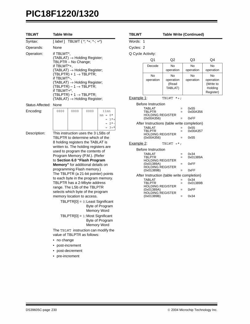
PIC18F1220/1320
TBLWT Table Write
Syntax: [ label ] TBLWT ( *; *+; *-; +*)
Operands: None
Operation: if TBLWT*,(TABLAT) → Holding Register;TBLPTR – No Change;if TBLWT*+,(TABLAT) → Holding Register;(TBLPTR) + 1 → TBLPTR;if TBLWT*-,(TABLAT) → Holding Register;(TBLPTR) – 1 → TBLPTR;if TBLWT+*,(TBLPTR) + 1 → TBLPTR;(TABLAT) → Holding Register;
Status Affected: None
Encoding: 0000 0000 0000 11nn nn = 0* = 1*+ = 2*- = 3+*
Description: This instruction uses the 3 LSBs of TBLPTR to determine which of the 8 holding registers the TABLAT is written to. The holding registers are used to program the contents of Program Memory (P.M.). (Refer to Section 6.0 “Flash Program Memory” for additional details on programming Flash memory.)The TBLPTR (a 21-bit pointer) points to each byte in the program memory. TBLPTR has a 2-Mbyte address range. The LSb of the TBLPTR selects which byte of the program memory location to access.
TBLPTR[0] = 0:Least Significant Byte of Program Memory Word
TBLPTR[0] = 1:Most Significant Byte of Program Memory Word
The TBLWT instruction can modify the value of TBLPTR as follows:
• no change• post-increment• post-decrement
• pre-increment
TBLWT Table Write (Continued)
Words: 1
Cycles: 2
Q Cycle Activity:
Q1 Q2 Q3 Q4
Decode No operation
No operation
No operation
No operation
No operation
(ReadTABLAT)
No operation
No operation(Write to Holding
Register)
Example 1: TBLWT *+;
Before InstructionTABLAT = 0x55TBLPTR = 0x00A356HOLDING REGISTER (0x00A356) = 0xFF
After Instructions (table write completion)TABLAT = 0x55TBLPTR = 0x00A357HOLDING REGISTER (0x00A356) = 0x55
Example 2: TBLWT +*;
Before InstructionTABLAT = 0x34TBLPTR = 0x01389AHOLDING REGISTER (0x01389A) = 0xFFHOLDING REGISTER (0x01389B) = 0xFF
After Instruction (table write completion)TABLAT = 0x34TBLPTR = 0x01389BHOLDING REGISTER (0x01389A) = 0xFFHOLDING REGISTER (0x01389B) = 0x34
DS39605C-page 230 2004 Microchip Technology Inc.

PIC18F1220/1320
TSTFSZ Test f, skip if 0
Syntax: [ label ] TSTFSZ f [,a]
Operands: 0 ≤ f ≤ 255a ∈ [0,1]
Operation: skip if f = 0
Status Affected: None
Encoding: 0110 011a ffff ffff
Description: If ‘f’ = 0, the next instruction, fetched during the current instruction execution is discarded and a NOP is executed, making this a two-cycle instruction. If ‘a’ is ‘0’, the Access Bank will be selected, overriding the BSR value. If ‘a’ is ‘1’, then the bank will be selected as per the BSR value (default).
Words: 1
Cycles: 1(2)Note: 3 cycles if skip and followed
by a 2-word instruction.
Q Cycle Activity:
Q1 Q2 Q3 Q4Decode Read
register ‘f’Process
DataNo
operation
If skip:
Q1 Q2 Q3 Q4No
operationNo
operationNo
operationNo
operation
If skip and followed by 2-word instruction:
Q1 Q2 Q3 Q4No
operationNo
operationNo
operationNo
operation
No operation
No operation
No operation
No operation
Example: HERE TSTFSZ CNTNZERO :ZERO :
Before InstructionPC = Address (HERE)
After InstructionIf CNT = 0x00,PC = Address (ZERO)If CNT ≠ 0x00,PC = Address (NZERO)
XORLW Exclusive OR literal with W
Syntax: [ label ] XORLW k
Operands: 0 ≤ k ≤ 255
Operation: (W) .XOR. k → W
Status Affected: N, Z
Encoding: 0000 1010 kkkk kkkk
Description: The contents of W are XOR’ed with the 8-bit literal ‘k’. The result is placed in W.
Words: 1
Cycles: 1
Q Cycle Activity:Q1 Q2 Q3 Q4
Decode Readliteral ‘k’
Process Data
Write to W
Example: XORLW 0xAF
Before Instruction
W = 0xB5
After Instruction
W = 0x1A
2004 Microchip Technology Inc. DS39605C-page 231
PIC18F1220/1320
XORWF Exclusive OR W with f
Syntax: [ label ] XORWF f [,d [,a]]
Operands: 0 ≤ f ≤ 255d ∈ [0,1]a ∈ [0,1]
Operation: (W) .XOR. (f) → dest
Status Affected: N, Z
Encoding: 0001 10da ffff ffff
Description: Exclusive OR the contents of W with register ‘f’. If ‘d’ is ‘0’, the result is stored in W. If ‘d’ is ‘1’, the result is stored back in the register ‘f’ (default). If ‘a’ is ‘0’, the Access Bank will be selected, overriding the BSR value. If ‘a’ is ‘1’, then the bank will be selected as per the BSR value (default).
Words: 1
Cycles: 1
Q Cycle Activity:Q1 Q2 Q3 Q4
Decode Readregister ‘f’
Process Data
Write to destination
Example: XORWF REG
Before InstructionREG = 0xAFW = 0xB5
After InstructionREG = 0x1AW = 0xB5
DS39605C-page 232 2004 Microchip Technology Inc.
PIC18F1220/1320
21.0 DEVELOPMENT SUPPORT
The PICmicro® microcontrollers are supported with afull range of hardware and software development tools:
• Integrated Development Environment
- MPLAB® IDE Software• Assemblers/Compilers/Linkers
- MPASMTM Assembler
- MPLAB C17 and MPLAB C18 C Compilers- MPLINKTM Object Linker/
MPLIBTM Object Librarian- MPLAB C30 C Compiler- MPLAB ASM30 Assembler/Linker/Library
• Simulators- MPLAB SIM Software Simulator- MPLAB dsPIC30 Software Simulator
• Emulators- MPLAB ICE 2000 In-Circuit Emulator- MPLAB ICE 4000 In-Circuit Emulator
• In-Circuit Debugger- MPLAB ICD 2
• Device Programmers
- PRO MATE® II Universal Device Programmer- PICSTART® Plus Development Programmer- MPLAB PM3 Device Programmer
• Low-Cost Demonstration Boards- PICDEMTM 1 Demonstration Board- PICDEM.netTM Demonstration Board
- PICDEM 2 Plus Demonstration Board- PICDEM 3 Demonstration Board- PICDEM 4 Demonstration Board
- PICDEM 17 Demonstration Board- PICDEM 18R Demonstration Board- PICDEM LIN Demonstration Board
- PICDEM USB Demonstration Board• Evaluation Kits
- KEELOQ® Evaluation and Programming Tools
- PICDEM MSC- microID® Developer Kits- CAN
- PowerSmart® Developer Kits- Analog
21.1 MPLAB Integrated Development Environment Software
The MPLAB IDE software brings an ease of softwaredevelopment previously unseen in the 8/16-bit micro-controller market. The MPLAB IDE is a Windows®
based application that contains:
• An interface to debugging tools- simulator- programmer (sold separately)
- emulator (sold separately)- in-circuit debugger (sold separately)
• A full-featured editor with color coded context
• A multiple project manager• Customizable data windows with direct edit of
contents• High-level source code debugging• Mouse over variable inspection
• Extensive on-line help
The MPLAB IDE allows you to:
• Edit your source files (either assembly or C)• One touch assemble (or compile) and download
to PICmicro emulator and simulator tools (automatically updates all project information)
• Debug using:- source files (assembly or C)- mixed assembly and C
- machine code
MPLAB IDE supports multiple debugging tools in asingle development paradigm, from the cost effectivesimulators, through low-cost in-circuit debuggers, tofull-featured emulators. This eliminates the learningcurve when upgrading to tools with increasing flexibilityand power.
21.2 MPASM Assembler
The MPASM assembler is a full-featured, universalmacro assembler for all PICmicro MCUs.
The MPASM assembler generates relocatable objectfiles for the MPLINK object linker, Intel® standard HEXfiles, MAP files to detail memory usage and symbol ref-erence, absolute LST files that contain source lines andgenerated machine code and COFF files fordebugging.
The MPASM assembler features include:
• Integration into MPLAB IDE projects• User defined macros to streamline assembly code
• Conditional assembly for multi-purpose source files
• Directives that allow complete control over the assembly process
2004 Microchip Technology Inc. DS39605C-page 233

PIC18F1220/1320
21.3 MPLAB C17 and MPLAB C18 C Compilers
The MPLAB C17 and MPLAB C18 Code DevelopmentSystems are complete ANSI C compilers forMicrochip’s PIC17CXXX and PIC18CXXX family ofmicrocontrollers. These compilers provide powerfulintegration capabilities, superior code optimization andease of use not found with other compilers.
For easy source level debugging, the compilers providesymbol information that is optimized to the MPLAB IDEdebugger.
21.4 MPLINK Object Linker/MPLIB Object Librarian
The MPLINK object linker combines relocatableobjects created by the MPASM assembler and theMPLAB C17 and MPLAB C18 C compilers. It can linkrelocatable objects from precompiled libraries, usingdirectives from a linker script.
The MPLIB object librarian manages the creation andmodification of library files of precompiled code. Whena routine from a library is called from a source file, onlythe modules that contain that routine will be linked inwith the application. This allows large libraries to beused efficiently in many different applications.
The object linker/library features include:
• Efficient linking of single libraries instead of many smaller files
• Enhanced code maintainability by grouping related modules together
• Flexible creation of libraries with easy module listing, replacement, deletion and extraction
21.5 MPLAB C30 C Compiler
The MPLAB C30 C compiler is a full-featured, ANSIcompliant, optimizing compiler that translates standardANSI C programs into dsPIC30F assembly languagesource. The compiler also supports many commandline options and language extensions to take fulladvantage of the dsPIC30F device hardware capabili-ties and afford fine control of the compiler codegenerator.
MPLAB C30 is distributed with a complete ANSI Cstandard library. All library functions have been vali-dated and conform to the ANSI C library standard. Thelibrary includes functions for string manipulation,dynamic memory allocation, data conversion, time-keeping and math functions (trigonometric, exponentialand hyperbolic). The compiler provides symbolicinformation for high-level source debugging with theMPLAB IDE.
21.6 MPLAB ASM30 Assembler, Linker and Librarian
MPLAB ASM30 assembler produces relocatablemachine code from symbolic assembly language fordsPIC30F devices. MPLAB C30 compiler uses theassembler to produce it’s object file. The assemblergenerates relocatable object files that can then bearchived or linked with other relocatable object files andarchives to create an executable file. Notable featuresof the assembler include:
• Support for the entire dsPIC30F instruction set
• Support for fixed-point and floating-point data• Command line interface• Rich directive set
• Flexible macro language• MPLAB IDE compatibility
21.7 MPLAB SIM Software Simulator
The MPLAB SIM software simulator allows code devel-opment in a PC hosted environment by simulating thePICmicro series microcontrollers on an instructionlevel. On any given instruction, the data areas can beexamined or modified and stimuli can be applied froma file, or user defined key press, to any pin. The execu-tion can be performed in Single-Step, Execute UntilBreak or Trace mode.
The MPLAB SIM simulator fully supports symbolicdebugging using the MPLAB C17 and MPLAB C18C Compilers, as well as the MPASM assembler. Thesoftware simulator offers the flexibility to develop anddebug code outside of the laboratory environment,making it an excellent, economical softwaredevelopment tool.
21.8 MPLAB SIM30 Software Simulator
The MPLAB SIM30 software simulator allows codedevelopment in a PC hosted environment by simulatingthe dsPIC30F series microcontrollers on an instructionlevel. On any given instruction, the data areas can beexamined or modified and stimuli can be applied froma file, or user defined key press, to any of the pins.
The MPLAB SIM30 simulator fully supports symbolicdebugging using the MPLAB C30 C Compiler andMPLAB ASM30 assembler. The simulator runs in eithera Command Line mode for automated tasks, or fromMPLAB IDE. This high-speed simulator is designed todebug, analyze and optimize time intensive DSProutines.
DS39605C-page 234 2004 Microchip Technology Inc.

PIC18F1220/1320
21.9 MPLAB ICE 2000 High-Performance Universal In-Circuit Emulator
The MPLAB ICE 2000 universal in-circuit emulator isintended to provide the product development engineerwith a complete microcontroller design tool set forPICmicro microcontrollers. Software control of theMPLAB ICE 2000 in-circuit emulator is advanced bythe MPLAB Integrated Development Environment,which allows editing, building, downloading and sourcedebugging from a single environment.
The MPLAB ICE 2000 is a full-featured emulator sys-tem with enhanced trace, trigger and data monitoringfeatures. Interchangeable processor modules allow thesystem to be easily reconfigured for emulation of differ-ent processors. The universal architecture of theMPLAB ICE in-circuit emulator allows expansion tosupport new PICmicro microcontrollers.
The MPLAB ICE 2000 in-circuit emulator system hasbeen designed as a real-time emulation system withadvanced features that are typically found on moreexpensive development tools. The PC platform andMicrosoft® Windows 32-bit operating system werechosen to best make these features available in asimple, unified application.
21.10 MPLAB ICE 4000 High-Performance Universal In-Circuit Emulator
The MPLAB ICE 4000 universal in-circuit emulator isintended to provide the product development engineerwith a complete microcontroller design tool set for high-end PICmicro microcontrollers. Software control of theMPLAB ICE in-circuit emulator is provided by theMPLAB Integrated Development Environment, whichallows editing, building, downloading and sourcedebugging from a single environment.
The MPLAB ICD 4000 is a premium emulator system,providing the features of MPLAB ICE 2000, but withincreased emulation memory and high-speed perfor-mance for dsPIC30F and PIC18XXXX devices. Itsadvanced emulator features include complex triggeringand timing, up to 2 Mb of emulation memory and theability to view variables in real-time.
The MPLAB ICE 4000 in-circuit emulator system hasbeen designed as a real-time emulation system withadvanced features that are typically found on moreexpensive development tools. The PC platform andMicrosoft Windows 32-bit operating system werechosen to best make these features available in asimple, unified application.
21.11 MPLAB ICD 2 In-Circuit Debugger
Microchip’s In-Circuit Debugger, MPLAB ICD 2, is apowerful, low-cost, run-time development tool,connecting to the host PC via an RS-232 or high-speedUSB interface. This tool is based on the FlashPICmicro MCUs and can be used to develop for theseand other PICmicro microcontrollers. The MPLABICD 2 utilizes the in-circuit debugging capability builtinto the Flash devices. This feature, along withMicrochip’s In-Circuit Serial ProgrammingTM (ICSPTM)protocol, offers cost effective in-circuit Flash debuggingfrom the graphical user interface of the MPLABIntegrated Development Environment. This enables adesigner to develop and debug source code by settingbreakpoints, single-stepping and watching variables,CPU status and peripheral registers. Running at fullspeed enables testing hardware and applications inreal-time. MPLAB ICD 2 also serves as a developmentprogrammer for selected PICmicro devices.
21.12 PRO MATE II Universal Device Programmer
The PRO MATE II is a universal, CE compliant deviceprogrammer with programmable voltage verification atVDDMIN and VDDMAX for maximum reliability. It featuresan LCD display for instructions and error messagesand a modular detachable socket assembly to supportvarious package types. In Stand-Alone mode, thePRO MATE II device programmer can read, verify andprogram PICmicro devices without a PC connection. Itcan also set code protection in this mode.
21.13 MPLAB PM3 Device Programmer
The MPLAB PM3 is a universal, CE compliant deviceprogrammer with programmable voltage verification atVDDMIN and VDDMAX for maximum reliability. It featuresa large LCD display (128 x 64) for menus and errormessages and a modular detachable socket assemblyto support various package types. The ICSP™ cableassembly is included as a standard item. In Stand-Alone mode, the MPLAB PM3 device programmer canread, verify and program PICmicro devices without aPC connection. It can also set code protection in thismode. MPLAB PM3 connects to the host PC via an RS-232 or USB cable. MPLAB PM3 has high-speed com-munications and optimized algorithms for quick pro-gramming of large memory devices and incorporatesan SD/MMC card for file storage and secure data appli-cations.
2004 Microchip Technology Inc. DS39605C-page 235
PIC18F1220/1320
21.14 PICSTART Plus Development Programmer
The PICSTART Plus development programmer is aneasy-to-use, low-cost, prototype programmer. It con-nects to the PC via a COM (RS-232) port. MPLABIntegrated Development Environment software makesusing the programmer simple and efficient. ThePICSTART Plus development programmer supportsmost PICmicro devices up to 40 pins. Larger pin countdevices, such as the PIC16C92X and PIC17C76X,may be supported with an adapter socket. ThePICSTART Plus development programmer is CEcompliant.
21.15 PICDEM 1 PICmicroDemonstration Board
The PICDEM 1 demonstration board demonstrates thecapabilities of the PIC16C5X (PIC16C54 toPIC16C58A), PIC16C61, PIC16C62X, PIC16C71,PIC16C8X, PIC17C42, PIC17C43 and PIC17C44. Allnecessary hardware and software is included to runbasic demo programs. The sample microcontrollersprovided with the PICDEM 1 demonstration board canbe programmed with a PRO MATE II device program-mer or a PICSTART Plus development programmer.The PICDEM 1 demonstration board can be connectedto the MPLAB ICE in-circuit emulator for testing. Aprototype area extends the circuitry for additional appli-cation components. Features include an RS-232interface, a potentiometer for simulated analog input,push button switches and eight LEDs.
21.16 PICDEM.net Internet/Ethernet Demonstration Board
The PICDEM.net demonstration board is an Internet/Ethernet demonstration board using the PIC18F452microcontroller and TCP/IP firmware. The boardsupports any 40-pin DIP device that conforms to thestandard pinout used by the PIC16F877 orPIC18C452. This kit features a user friendly TCP/IPstack, web server with HTML, a 24L256 SerialEEPROM for Xmodem download to web pages intoSerial EEPROM, ICSP/MPLAB ICD 2 interface con-nector, an Ethernet interface, RS-232 interface and a16 x 2 LCD display. Also included is the book andCD-ROM “TCP/IP Lean, Web Servers for EmbeddedSystems,” by Jeremy Bentham
21.17 PICDEM 2 Plus Demonstration Board
The PICDEM 2 Plus demonstration board supportsmany 18, 28 and 40-pin microcontrollers, includingPIC16F87X and PIC18FXX2 devices. All the neces-sary hardware and software is included to run the dem-onstration programs. The sample microcontrollersprovided with the PICDEM 2 demonstration board canbe programmed with a PRO MATE II device program-mer, PICSTART Plus development programmer, orMPLAB ICD 2 with a Universal Programmer Adapter.The MPLAB ICD 2 and MPLAB ICE in-circuit emulatorsmay also be used with the PICDEM 2 demonstrationboard to test firmware. A prototype area extends thecircuitry for additional application components. Someof the features include an RS-232 interface, a 2 x 16LCD display, a piezo speaker, an on-board temperaturesensor, four LEDs and sample PIC18F452 andPIC16F877 Flash microcontrollers.
21.18 PICDEM 3 PIC16C92X Demonstration Board
The PICDEM 3 demonstration board supports thePIC16C923 and PIC16C924 in the PLCC package. Allthe necessary hardware and software is included to runthe demonstration programs.
21.19 PICDEM 4 8/14/18-Pin Demonstration Board
The PICDEM 4 can be used to demonstrate the capa-bilities of the 8, 14 and 18-pin PIC16XXXX andPIC18XXXX MCUs, including the PIC16F818/819,PIC16F87/88, PIC16F62XA and the PIC18F1320family of microcontrollers. PICDEM 4 is intended toshowcase the many features of these low pin countparts, including LIN and Motor Control using ECCP.Special provisions are made for low-power operationwith the supercapacitor circuit and jumpers allow on-board hardware to be disabled to eliminate currentdraw in this mode. Included on the demo board are pro-visions for Crystal, RC or Canned Oscillator modes, afive volt regulator for use with a nine volt wall adapteror battery, DB-9 RS-232 interface, ICD connector forprogramming via ICSP and development with MPLABICD 2, 2 x 16 liquid crystal display, PCB footprints forH-Bridge motor driver, LIN transceiver and EEPROM.Also included are: header for expansion, eight LEDs,four potentiometers, three push buttons and a proto-typing area. Included with the kit is a PIC16F627A anda PIC18F1320. Tutorial firmware is included alongwith the User’s Guide.
DS39605C-page 236 2004 Microchip Technology Inc.
PIC18F1220/1320
21.20 PICDEM 17 Demonstration Board
The PICDEM 17 demonstration board is an evaluationboard that demonstrates the capabilities of severalMicrochip microcontrollers, including PIC17C752,PIC17C756A, PIC17C762 and PIC17C766. A pro-grammed sample is included. The PRO MATE II deviceprogrammer, or the PICSTART Plus development pro-grammer, can be used to reprogram the device for usertailored application development. The PICDEM 17demonstration board supports program download andexecution from external on-board Flash memory. Agenerous prototype area is available for user hardwareexpansion.
21.21 PICDEM 18R PIC18C601/801 Demonstration Board
The PICDEM 18R demonstration board serves to assistdevelopment of the PIC18C601/801 family of Microchipmicrocontrollers. It provides hardware implementationof both 8-bit Multiplexed/Demultiplexed and 16-bitMemory modes. The board includes 2 Mb externalFlash memory and 128 Kb SRAM memory, as well asserial EEPROM, allowing access to the wide range ofmemory types supported by the PIC18C601/801.
21.22 PICDEM LIN PIC16C43X Demonstration Board
The powerful LIN hardware and software kit includes aseries of boards and three PICmicro microcontrollers.The small footprint PIC16C432 and PIC16C433 areused as slaves in the LIN communication and featureon-board LIN transceivers. A PIC16F874 Flashmicrocontroller serves as the master. All three micro-controllers are programmed with firmware to provideLIN bus communication.
21.23 PICkitTM 1 Flash Starter Kit
A complete “development system in a box”, the PICkit™Flash Starter Kit includes a convenient multi-sectionboard for programming, evaluation and development of8/14-pin Flash PIC® microcontrollers. Powered via USB,the board operates under a simple Windows GUI. ThePICkit 1 Starter Kit includes the User’s Guide (on CDROM), PICkit 1 tutorial software and code for variousapplications. Also included are MPLAB® IDE (IntegratedDevelopment Environment) software, software andhardware “Tips 'n Tricks for 8-pin Flash PIC®
Microcontrollers” Handbook and a USB interface cable.Supports all current 8/14-pin Flash PIC microcontrollers,as well as many future planned devices.
21.24 PICDEM USB PIC16C7X5 Demonstration Board
The PICDEM USB Demonstration Board shows off thecapabilities of the PIC16C745 and PIC16C765 USBmicrocontrollers. This board provides the basis forfuture USB products.
21.25 Evaluation and Programming Tools
In addition to the PICDEM series of circuits, Microchiphas a line of evaluation kits and demonstration softwarefor these products.
• KEELOQ evaluation and programming tools for Microchip’s HCS Secure Data Products
• CAN developers kit for automotive network applications
• Analog design boards and filter design software
• PowerSmart battery charging evaluation/calibration kits
• IrDA® development kit• microID development and rfLabTM development
software• SEEVAL® designer kit for memory evaluation and
endurance calculations• PICDEM MSC demo boards for Switching mode
power supply, high-power IR driver, delta sigma ADC and flow rate sensor
Check the Microchip web page and the latest ProductSelector Guide for the complete list of demonstrationand evaluation kits.
2004 Microchip Technology Inc. DS39605C-page 237

PIC18F1220/1320
NOTES:
DS39605C-page 238 2004 Microchip Technology Inc.

PIC18F1220/1320
22.0 ELECTRICAL CHARACTERISTICS
Absolute Maximum Ratings(†)
Ambient temperature under bias............................................................................................................ .-40°C to +125°C
Storage temperature .............................................................................................................................. -65°C to +150°C
Voltage on any pin with respect to VSS (except VDD, MCLR and RA4) .......................................... -0.3V to (VDD + 0.3V)
Voltage on VDD with respect to VSS ......................................................................................................... -0.3V to +5.5V
Voltage on MCLR with respect to VSS (Note 2) ......................................................................................... 0V to +13.25V
Voltage on RA4 with respect to Vss ............................................................................................................... 0V to +8.5V
Total power dissipation (Note 1) ...............................................................................................................................1.0W
Maximum current out of VSS pin ...........................................................................................................................300 mA
Maximum current into VDD pin ..............................................................................................................................250 mA
Input clamp current, IIK (VI < 0 or VI > VDD)...................................................................................................................... ±20 mA
Output clamp current, IOK (VO < 0 or VO > VDD) .............................................................................................................. ±20 mA
Maximum output current sunk by any I/O pin..........................................................................................................25 mA
Maximum output current sourced by any I/O pin ....................................................................................................25 mA
Maximum current sunk by all ports .......................................................................................................................200 mA
Maximum current sourced by all ports ..................................................................................................................200 mA
Note 1: Power dissipation is calculated as follows: Pdis = VDD x IDD – ∑ IOH + ∑ (VDD – VOH) x IOH + ∑(VOL x IOL)
2: Voltage spikes below VSS at the MCLR/VPP pin, inducing currents greater than 80 mA, may cause latch-up.Thus, a series resistor of 50-100Ω should be used when applying a “low” level to the MCLR/VPP pin, ratherthan pulling this pin directly to VSS.
† NOTICE: Stresses above those listed under “Absolute Maximum Ratings” may cause permanent damage to the device. This is a stress rating only and functional operation of the device at those or any other conditions above those indicated in the operation listings of this specification is not implied. Exposure to maximum rating conditions for extended periods may affect device reliability.
2004 Microchip Technology Inc. DS39605C-page 239
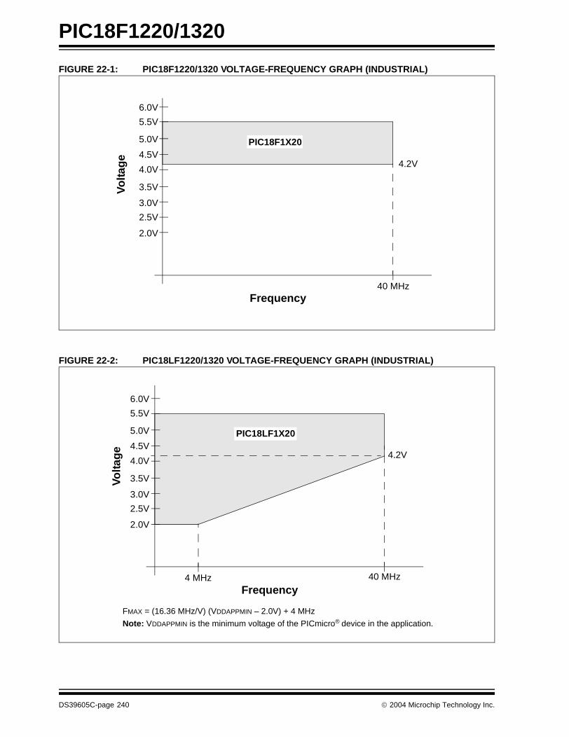
PIC18F1220/1320
FIGURE 22-1: PIC18F1220/1320 VOLTAGE-FREQUENCY GRAPH (INDUSTRIAL)
FIGURE 22-2: PIC18LF1220/1320 VOLTAGE-FREQUENCY GRAPH (INDUSTRIAL)
Frequency
Vo
ltag
e6.0V
5.5V
4.5V
4.0V
2.0V
40 MHz
5.0V
3.5V
3.0V
2.5V
PIC18F1X20
4.2V
Frequency
Volta
ge
6.0V
5.5V
4.5V
4.0V
2.0V
40 MHz
5.0V
3.5V
3.0V
2.5V
FMAX = (16.36 MHz/V) (VDDAPPMIN – 2.0V) + 4 MHz
Note: VDDAPPMIN is the minimum voltage of the PICmicro® device in the application.
4 MHz
4.2V
PIC18LF1X20
DS39605C-page 240 2004 Microchip Technology Inc.

PIC18F1220/1320
FIGURE 22-3: PIC18F1220/1320 VOLTAGE-FREQUENCY GRAPH (EXTENDED)Frequency
Vo
ltag
e
6.0V
5.5V
4.5V
4.0V
2.0V
25 MHz
5.0V
3.5V
3.0V
2.5V
PIC18F1X20-E
4.2V
2004 Microchip Technology Inc. DS39605C-page 241

PIC18F1220/1320
22.1 DC Characteristics: Supply VoltagePIC18F1220/1320 (Industrial) PIC18LF1220/1320 (Industrial)
PIC18LF1220/1320 (Industrial)
Standard Operating Conditions (unless otherwise stated)Operating temperature -40°C ≤ TA ≤ +85°C for industrial
PIC18F1220/1320 (Industrial, Extended)
Standard Operating Conditions (unless otherwise stated)Operating temperature -40°C ≤ TA ≤ +85°C for industrial
-40°C ≤ TA ≤ +125°C for extended
Param No.
Symbol Characteristic Min Typ Max Units Conditions
VDD Supply Voltage
D001 PIC18LF1220/1320 2.0 — 5.5 V HS, XT, RC and LP Oscillator mode
PIC18F1220/1320 4.2 — 5.5 V
D002 VDR RAM Data RetentionVoltage(1)
1.5 — — V
D003 VPOR VDD Start Voltage to ensure internal Power-on Reset signal
— — 0.7 V See Section 4.1 “Power-on Reset (POR)” for details.
D004 SVDD VDD Rise Rate to ensureinternal Power-on Reset signal
0.05 — — V/ms See Section 4.1 “Power-on Reset (POR)” for details.
VBOR Brown-out Reset Voltage
D005D PIC18LF1220/1320 Industrial Low Voltage (-10°C to +85°C)
BORV1:BORV0 = 11 N/A N/A N/A V Reserved
BORV1:BORV0 = 10 2.50 2.72 2.94 V
BORV1:BORV0 = 01 3.88 4.22 4.56 V (Note 2)
BORV1:BORV0 = 00 4.18 4.54 4.90 V (Note 2)
D005F PIC18LF1220/1320 Industrial Low Voltage (-40°C to -10°C)
BORV1:BORV0 = 11 N/A N/A N/A V Reserved
BORV1:BORV0 = 10 2.34 2.72 3.10 V
BORV1:BORV0 = 01 3.63 4.22 4.81 V (Note 2)
BORV1:BORV0 = 00 3.90 4.54 5.18 V (Note 2)
D005G PIC18F1220/1320 Industrial (-10°C to +85°C)
BORV1:BORV0 = 1x N/A N/A N/A V Reserved
BORV1:BORV0 = 01 3.88 4.22 4.56 V (Note 2)
BORV1:BORV0 = 00 4.18 4.54 4.90 V (Note 2)
D005H PIC18F1220/1320 Industrial (-40°C to -10°C)
BORV1:BORV0 = 1x N/A N/A N/A V Reserved
BORV1:BORV0 = 01 N/A N/A N/A V Reserved
BORV1:BORV0 = 00 3.90 4.54 5.18 V (Note 2)
D005J PIC18F1220/1320 Extended (-10°C to +85°C)
BORV1:BORV0 = 1x N/A N/A N/A V Reserved
BORV1:BORV0 = 01 3.88 4.22 4.56 V (Note 3)
BORV1:BORV0 = 00 4.18 4.54 4.90 V (Note 3)
D005K PIC18F1220/1320 Extended (-40°C to -10°C, +85°C to +125°C)
BORV1:BORV0 = 1x N/A N/A N/A V Reserved
BORV1:BORV0 = 01 N/A N/A N/A V Reserved
BORV1:BORV0 = 00 3.90 4.54 5.18 V (Note 3)
Legend: Shading of rows is to assist in readability of the table.Note 1: This is the limit to which VDD can be lowered in Sleep mode, or during a device Reset, without losing RAM data.
2: When BOR is on and BORV<1:0> = 0x, the device will operate correctly at 40 MHz for any VDD at which the BOR allows execution (low-voltage and industrial devices only).
3: When BOR is on and BORV<1:0> = 0x, the device will operate correctly at 25 MHz for any VDD at which the BOR allows execution (extended devices only).
DS39605C-page 242 2004 Microchip Technology Inc.
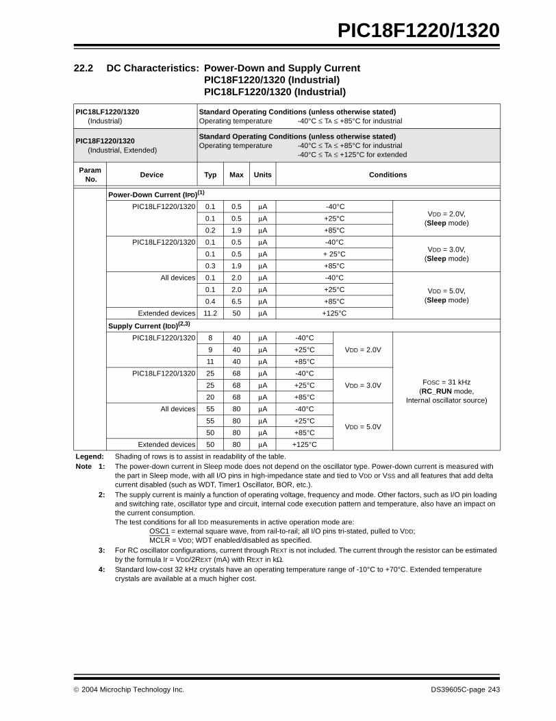
PIC18F1220/1320
22.2 DC Characteristics: Power-Down and Supply CurrentPIC18F1220/1320 (Industrial) PIC18LF1220/1320 (Industrial)
PIC18LF1220/1320 (Industrial)
Standard Operating Conditions (unless otherwise stated)Operating temperature -40°C ≤ TA ≤ +85°C for industrial
PIC18F1220/1320 (Industrial, Extended)
Standard Operating Conditions (unless otherwise stated)Operating temperature -40°C ≤ TA ≤ +85°C for industrial
-40°C ≤ TA ≤ +125°C for extended
Param No.
Device Typ Max Units Conditions
Power-Down Current (IPD)(1)
PIC18LF1220/1320 0.1 0.5 µA -40°CVDD = 2.0V,
(Sleep mode)0.1 0.5 µA +25°C
0.2 1.9 µA +85°C
PIC18LF1220/1320 0.1 0.5 µA -40°CVDD = 3.0V,
(Sleep mode)0.1 0.5 µA + 25°C
0.3 1.9 µA +85°C
All devices 0.1 2.0 µA -40°C
VDD = 5.0V,(Sleep mode)
0.1 2.0 µA +25°C
0.4 6.5 µA +85°C
Extended devices 11.2 50 µA +125°C
Supply Current (IDD)(2,3)
PIC18LF1220/1320 8 40 µA -40°C
FOSC = 31 kHz(RC_RUN mode,
Internal oscillator source)
9 40 µA +25°C VDD = 2.0V
11 40 µA +85°C
PIC18LF1220/1320 25 68 µA -40°C
25 68 µA +25°C VDD = 3.0V
20 68 µA +85°C
All devices 55 80 µA -40°C
VDD = 5.0V55 80 µA +25°C
50 80 µA +85°C
Extended devices 50 80 µA +125°C
Legend: Shading of rows is to assist in readability of the table.Note 1: The power-down current in Sleep mode does not depend on the oscillator type. Power-down current is measured with
the part in Sleep mode, with all I/O pins in high-impedance state and tied to VDD or VSS and all features that add delta current disabled (such as WDT, Timer1 Oscillator, BOR, etc.).
2: The supply current is mainly a function of operating voltage, frequency and mode. Other factors, such as I/O pin loading and switching rate, oscillator type and circuit, internal code execution pattern and temperature, also have an impact on the current consumption.The test conditions for all IDD measurements in active operation mode are:
OSC1 = external square wave, from rail-to-rail; all I/O pins tri-stated, pulled to VDD;MCLR = VDD; WDT enabled/disabled as specified.
3: For RC oscillator configurations, current through REXT is not included. The current through the resistor can be estimated by the formula Ir = VDD/2REXT (mA) with REXT in kΩ.
4: Standard low-cost 32 kHz crystals have an operating temperature range of -10°C to +70°C. Extended temperature crystals are available at a much higher cost.
2004 Microchip Technology Inc. DS39605C-page 243
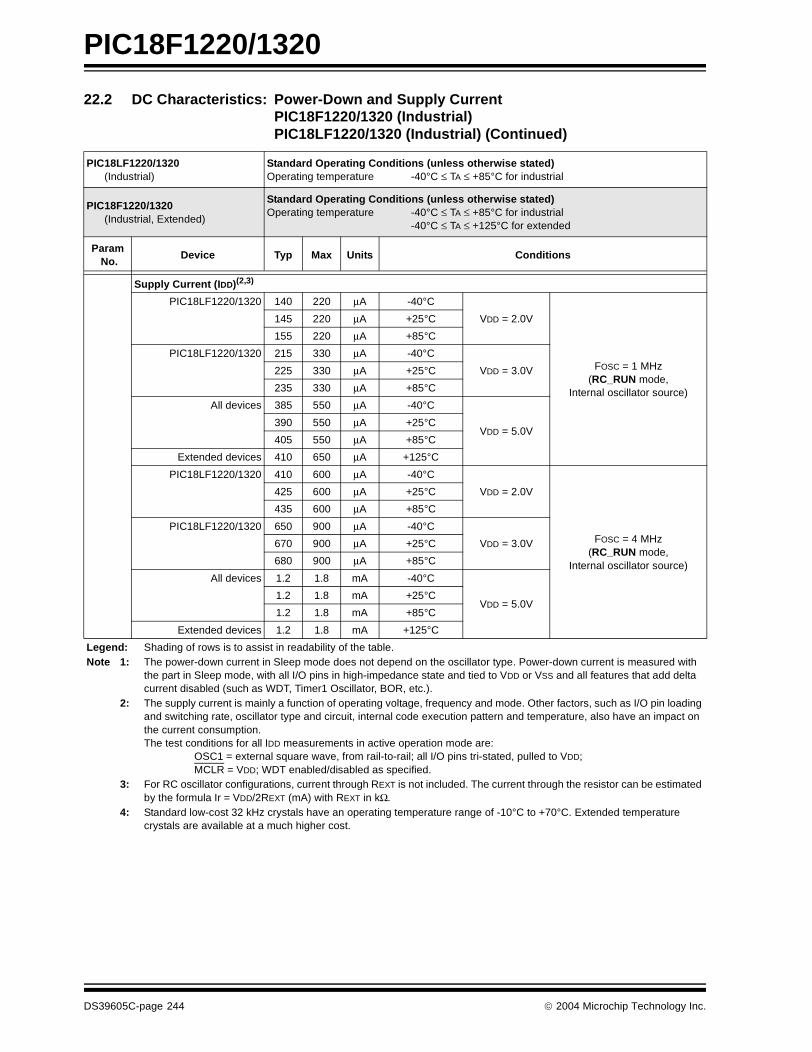
PIC18F1220/1320
Supply Current (IDD)(2,3)
PIC18LF1220/1320 140 220 µA -40°C
FOSC = 1 MHz(RC_RUN mode,
Internal oscillator source)
145 220 µA +25°C VDD = 2.0V
155 220 µA +85°C
PIC18LF1220/1320 215 330 µA -40°C
225 330 µA +25°C VDD = 3.0V
235 330 µA +85°C
All devices 385 550 µA -40°C
VDD = 5.0V390 550 µA +25°C
405 550 µA +85°C
Extended devices 410 650 µA +125°C
PIC18LF1220/1320 410 600 µA -40°C
FOSC = 4 MHz(RC_RUN mode,
Internal oscillator source)
425 600 µA +25°C VDD = 2.0V
435 600 µA +85°C
PIC18LF1220/1320 650 900 µA -40°C
670 900 µA +25°C VDD = 3.0V
680 900 µA +85°C
All devices 1.2 1.8 mA -40°C
VDD = 5.0V1.2 1.8 mA +25°C
1.2 1.8 mA +85°C
Extended devices 1.2 1.8 mA +125°C
22.2 DC Characteristics: Power-Down and Supply CurrentPIC18F1220/1320 (Industrial) PIC18LF1220/1320 (Industrial) (Continued)
PIC18LF1220/1320 (Industrial)
Standard Operating Conditions (unless otherwise stated)Operating temperature -40°C ≤ TA ≤ +85°C for industrial
PIC18F1220/1320 (Industrial, Extended)
Standard Operating Conditions (unless otherwise stated)Operating temperature -40°C ≤ TA ≤ +85°C for industrial
-40°C ≤ TA ≤ +125°C for extended
Param No.
Device Typ Max Units Conditions
Legend: Shading of rows is to assist in readability of the table.Note 1: The power-down current in Sleep mode does not depend on the oscillator type. Power-down current is measured with
the part in Sleep mode, with all I/O pins in high-impedance state and tied to VDD or VSS and all features that add delta current disabled (such as WDT, Timer1 Oscillator, BOR, etc.).
2: The supply current is mainly a function of operating voltage, frequency and mode. Other factors, such as I/O pin loading and switching rate, oscillator type and circuit, internal code execution pattern and temperature, also have an impact on the current consumption.The test conditions for all IDD measurements in active operation mode are:
OSC1 = external square wave, from rail-to-rail; all I/O pins tri-stated, pulled to VDD;MCLR = VDD; WDT enabled/disabled as specified.
3: For RC oscillator configurations, current through REXT is not included. The current through the resistor can be estimated by the formula Ir = VDD/2REXT (mA) with REXT in kΩ.
4: Standard low-cost 32 kHz crystals have an operating temperature range of -10°C to +70°C. Extended temperature crystals are available at a much higher cost.
DS39605C-page 244 2004 Microchip Technology Inc.
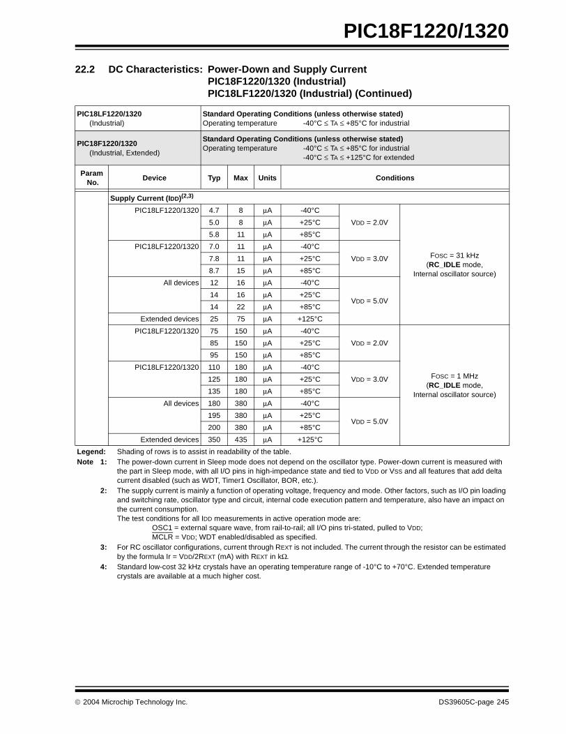
PIC18F1220/1320
Supply Current (IDD)(2,3)
PIC18LF1220/1320 4.7 8 µA -40°C
FOSC = 31 kHz(RC_IDLE mode,
Internal oscillator source)
5.0 8 µA +25°C VDD = 2.0V
5.8 11 µA +85°C
PIC18LF1220/1320 7.0 11 µA -40°C
7.8 11 µA +25°C VDD = 3.0V
8.7 15 µA +85°C
All devices 12 16 µA -40°C
VDD = 5.0V14 16 µA +25°C
14 22 µA +85°C
Extended devices 25 75 µA +125°C
PIC18LF1220/1320 75 150 µA -40°C
FOSC = 1 MHz(RC_IDLE mode,
Internal oscillator source)
85 150 µA +25°C VDD = 2.0V
95 150 µA +85°C
PIC18LF1220/1320 110 180 µA -40°C
125 180 µA +25°C VDD = 3.0V
135 180 µA +85°C
All devices 180 380 µA -40°C
VDD = 5.0V195 380 µA +25°C
200 380 µA +85°C
Extended devices 350 435 µA +125°C
22.2 DC Characteristics: Power-Down and Supply CurrentPIC18F1220/1320 (Industrial) PIC18LF1220/1320 (Industrial) (Continued)
PIC18LF1220/1320 (Industrial)
Standard Operating Conditions (unless otherwise stated)Operating temperature -40°C ≤ TA ≤ +85°C for industrial
PIC18F1220/1320 (Industrial, Extended)
Standard Operating Conditions (unless otherwise stated)Operating temperature -40°C ≤ TA ≤ +85°C for industrial
-40°C ≤ TA ≤ +125°C for extended
Param No.
Device Typ Max Units Conditions
Legend: Shading of rows is to assist in readability of the table.Note 1: The power-down current in Sleep mode does not depend on the oscillator type. Power-down current is measured with
the part in Sleep mode, with all I/O pins in high-impedance state and tied to VDD or VSS and all features that add delta current disabled (such as WDT, Timer1 Oscillator, BOR, etc.).
2: The supply current is mainly a function of operating voltage, frequency and mode. Other factors, such as I/O pin loading and switching rate, oscillator type and circuit, internal code execution pattern and temperature, also have an impact on the current consumption.The test conditions for all IDD measurements in active operation mode are:
OSC1 = external square wave, from rail-to-rail; all I/O pins tri-stated, pulled to VDD;MCLR = VDD; WDT enabled/disabled as specified.
3: For RC oscillator configurations, current through REXT is not included. The current through the resistor can be estimated by the formula Ir = VDD/2REXT (mA) with REXT in kΩ.
4: Standard low-cost 32 kHz crystals have an operating temperature range of -10°C to +70°C. Extended temperature crystals are available at a much higher cost.
2004 Microchip Technology Inc. DS39605C-page 245
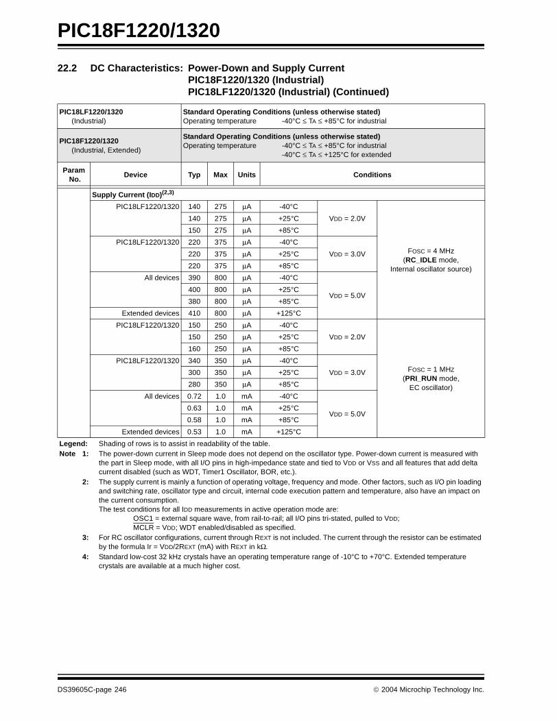
PIC18F1220/1320
Supply Current (IDD)(2,3)
PIC18LF1220/1320 140 275 µA -40°C
FOSC = 4 MHz(RC_IDLE mode,
Internal oscillator source)
140 275 µA +25°C VDD = 2.0V
150 275 µA +85°C
PIC18LF1220/1320 220 375 µA -40°C
220 375 µA +25°C VDD = 3.0V
220 375 µA +85°C
All devices 390 800 µA -40°C
VDD = 5.0V400 800 µA +25°C
380 800 µA +85°C
Extended devices 410 800 µA +125°C
PIC18LF1220/1320 150 250 µA -40°C
FOSC = 1 MHZ
(PRI_RUN mode,EC oscillator)
150 250 µA +25°C VDD = 2.0V
160 250 µA +85°C
PIC18LF1220/1320 340 350 µA -40°C
300 350 µA +25°C VDD = 3.0V
280 350 µA +85°C
All devices 0.72 1.0 mA -40°C
VDD = 5.0V0.63 1.0 mA +25°C
0.58 1.0 mA +85°C
Extended devices 0.53 1.0 mA +125°C
22.2 DC Characteristics: Power-Down and Supply CurrentPIC18F1220/1320 (Industrial) PIC18LF1220/1320 (Industrial) (Continued)
PIC18LF1220/1320 (Industrial)
Standard Operating Conditions (unless otherwise stated)Operating temperature -40°C ≤ TA ≤ +85°C for industrial
PIC18F1220/1320 (Industrial, Extended)
Standard Operating Conditions (unless otherwise stated)Operating temperature -40°C ≤ TA ≤ +85°C for industrial
-40°C ≤ TA ≤ +125°C for extended
Param No.
Device Typ Max Units Conditions
Legend: Shading of rows is to assist in readability of the table.Note 1: The power-down current in Sleep mode does not depend on the oscillator type. Power-down current is measured with
the part in Sleep mode, with all I/O pins in high-impedance state and tied to VDD or VSS and all features that add delta current disabled (such as WDT, Timer1 Oscillator, BOR, etc.).
2: The supply current is mainly a function of operating voltage, frequency and mode. Other factors, such as I/O pin loading and switching rate, oscillator type and circuit, internal code execution pattern and temperature, also have an impact on the current consumption.The test conditions for all IDD measurements in active operation mode are:
OSC1 = external square wave, from rail-to-rail; all I/O pins tri-stated, pulled to VDD;MCLR = VDD; WDT enabled/disabled as specified.
3: For RC oscillator configurations, current through REXT is not included. The current through the resistor can be estimated by the formula Ir = VDD/2REXT (mA) with REXT in kΩ.
4: Standard low-cost 32 kHz crystals have an operating temperature range of -10°C to +70°C. Extended temperature crystals are available at a much higher cost.
DS39605C-page 246 2004 Microchip Technology Inc.
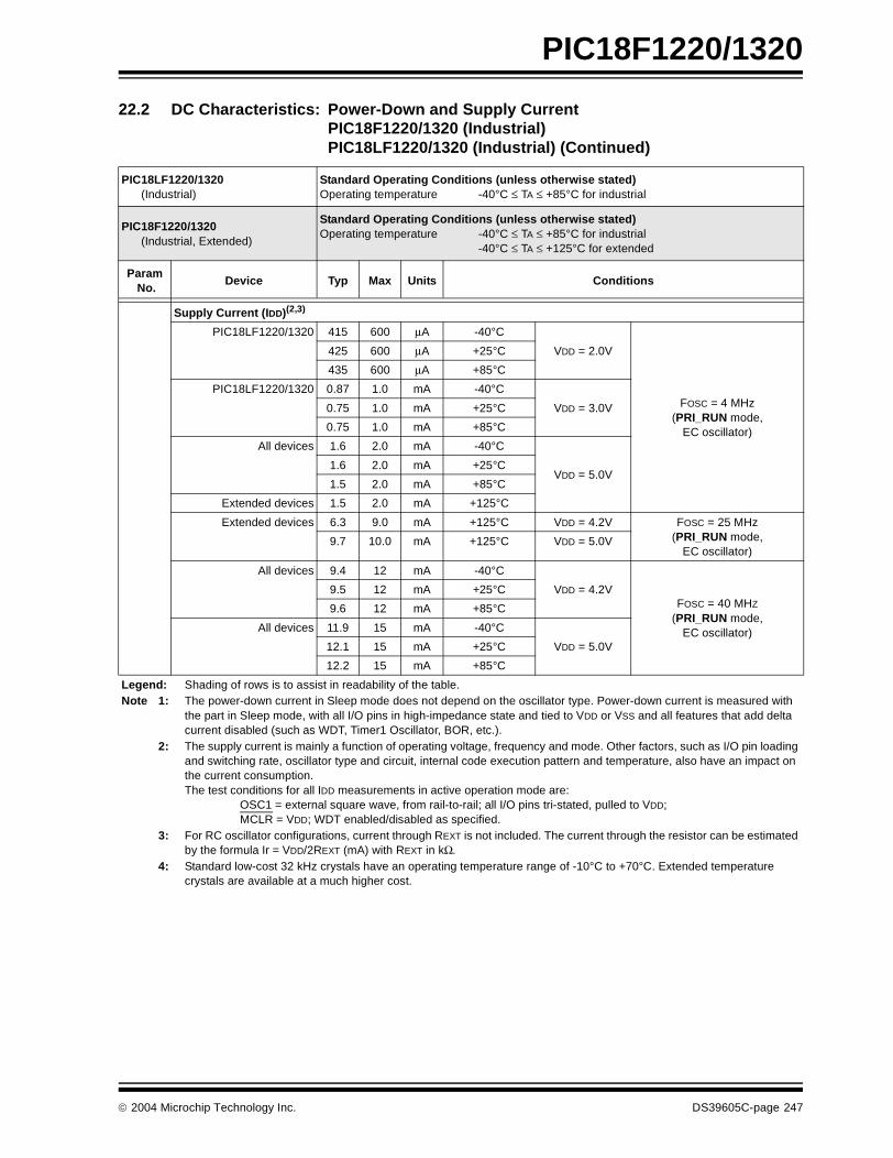
PIC18F1220/1320
Supply Current (IDD)(2,3)
PIC18LF1220/1320 415 600 µA -40°C
FOSC = 4 MHz(PRI_RUN mode,
EC oscillator)
425 600 µA +25°C VDD = 2.0V
435 600 µA +85°C
PIC18LF1220/1320 0.87 1.0 mA -40°C
0.75 1.0 mA +25°C VDD = 3.0V
0.75 1.0 mA +85°C
All devices 1.6 2.0 mA -40°C
VDD = 5.0V1.6 2.0 mA +25°C
1.5 2.0 mA +85°C
Extended devices 1.5 2.0 mA +125°C
Extended devices 6.3 9.0 mA +125°C VDD = 4.2V FOSC = 25 MHz(PRI_RUN mode,
EC oscillator)9.7 10.0 mA +125°C VDD = 5.0V
All devices 9.4 12 mA -40°C
FOSC = 40 MHZ
(PRI_RUN mode,EC oscillator)
9.5 12 mA +25°C VDD = 4.2V
9.6 12 mA +85°C
All devices 11.9 15 mA -40°C
VDD = 5.0V12.1 15 mA +25°C
12.2 15 mA +85°C
22.2 DC Characteristics: Power-Down and Supply CurrentPIC18F1220/1320 (Industrial) PIC18LF1220/1320 (Industrial) (Continued)
PIC18LF1220/1320 (Industrial)
Standard Operating Conditions (unless otherwise stated)Operating temperature -40°C ≤ TA ≤ +85°C for industrial
PIC18F1220/1320 (Industrial, Extended)
Standard Operating Conditions (unless otherwise stated)Operating temperature -40°C ≤ TA ≤ +85°C for industrial
-40°C ≤ TA ≤ +125°C for extended
Param No.
Device Typ Max Units Conditions
Legend: Shading of rows is to assist in readability of the table.Note 1: The power-down current in Sleep mode does not depend on the oscillator type. Power-down current is measured with
the part in Sleep mode, with all I/O pins in high-impedance state and tied to VDD or VSS and all features that add delta current disabled (such as WDT, Timer1 Oscillator, BOR, etc.).
2: The supply current is mainly a function of operating voltage, frequency and mode. Other factors, such as I/O pin loading and switching rate, oscillator type and circuit, internal code execution pattern and temperature, also have an impact on the current consumption.The test conditions for all IDD measurements in active operation mode are:
OSC1 = external square wave, from rail-to-rail; all I/O pins tri-stated, pulled to VDD;MCLR = VDD; WDT enabled/disabled as specified.
3: For RC oscillator configurations, current through REXT is not included. The current through the resistor can be estimated by the formula Ir = VDD/2REXT (mA) with REXT in kΩ.
4: Standard low-cost 32 kHz crystals have an operating temperature range of -10°C to +70°C. Extended temperature crystals are available at a much higher cost.
2004 Microchip Technology Inc. DS39605C-page 247
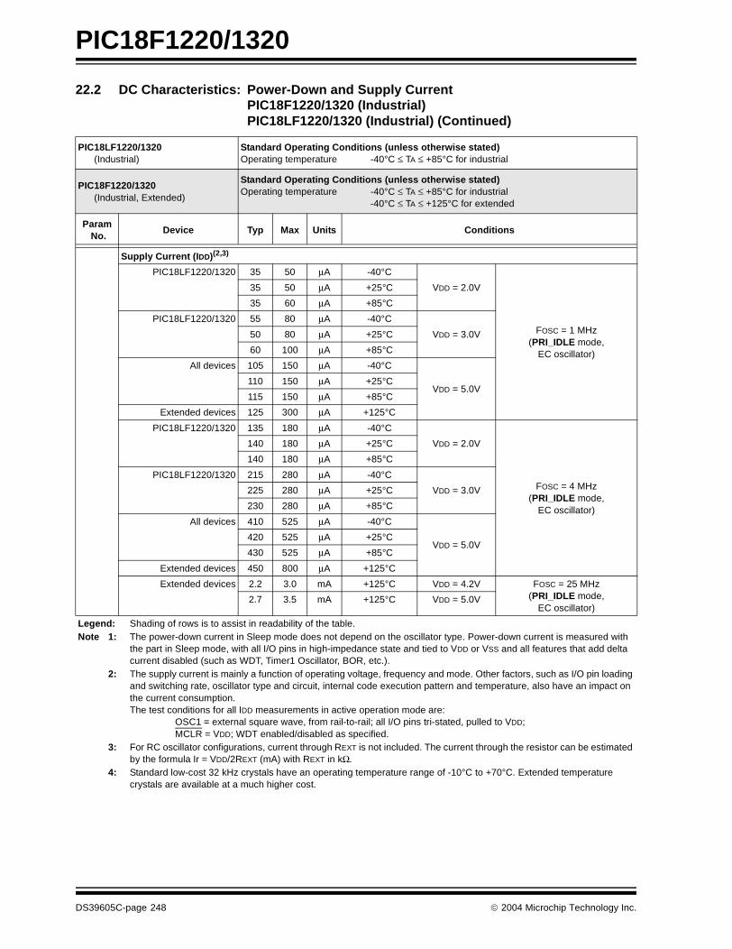
PIC18F1220/1320
Supply Current (IDD)(2,3)
PIC18LF1220/1320 35 50 µA -40°C
FOSC = 1 MHz(PRI_IDLE mode,
EC oscillator)
35 50 µA +25°C VDD = 2.0V
35 60 µA +85°C
PIC18LF1220/1320 55 80 µA -40°C
50 80 µA +25°C VDD = 3.0V
60 100 µA +85°C
All devices 105 150 µA -40°C
VDD = 5.0V110 150 µA +25°C
115 150 µA +85°C
Extended devices 125 300 µA +125°C
PIC18LF1220/1320 135 180 µA -40°C
FOSC = 4 MHz(PRI_IDLE mode,
EC oscillator)
140 180 µA +25°C VDD = 2.0V
140 180 µA +85°C
PIC18LF1220/1320 215 280 µA -40°C
225 280 µA +25°C VDD = 3.0V
230 280 µA +85°C
All devices 410 525 µA -40°C
VDD = 5.0V420 525 µA +25°C
430 525 µA +85°C
Extended devices 450 800 µA +125°C
Extended devices 2.2 3.0 mA +125°C VDD = 4.2V FOSC = 25 MHz(PRI_IDLE mode,
EC oscillator)2.7 3.5 mA +125°C VDD = 5.0V
22.2 DC Characteristics: Power-Down and Supply CurrentPIC18F1220/1320 (Industrial) PIC18LF1220/1320 (Industrial) (Continued)
PIC18LF1220/1320 (Industrial)
Standard Operating Conditions (unless otherwise stated)Operating temperature -40°C ≤ TA ≤ +85°C for industrial
PIC18F1220/1320 (Industrial, Extended)
Standard Operating Conditions (unless otherwise stated)Operating temperature -40°C ≤ TA ≤ +85°C for industrial
-40°C ≤ TA ≤ +125°C for extended
Param No.
Device Typ Max Units Conditions
Legend: Shading of rows is to assist in readability of the table.Note 1: The power-down current in Sleep mode does not depend on the oscillator type. Power-down current is measured with
the part in Sleep mode, with all I/O pins in high-impedance state and tied to VDD or VSS and all features that add delta current disabled (such as WDT, Timer1 Oscillator, BOR, etc.).
2: The supply current is mainly a function of operating voltage, frequency and mode. Other factors, such as I/O pin loading and switching rate, oscillator type and circuit, internal code execution pattern and temperature, also have an impact on the current consumption.The test conditions for all IDD measurements in active operation mode are:
OSC1 = external square wave, from rail-to-rail; all I/O pins tri-stated, pulled to VDD;MCLR = VDD; WDT enabled/disabled as specified.
3: For RC oscillator configurations, current through REXT is not included. The current through the resistor can be estimated by the formula Ir = VDD/2REXT (mA) with REXT in kΩ.
4: Standard low-cost 32 kHz crystals have an operating temperature range of -10°C to +70°C. Extended temperature crystals are available at a much higher cost.
DS39605C-page 248 2004 Microchip Technology Inc.
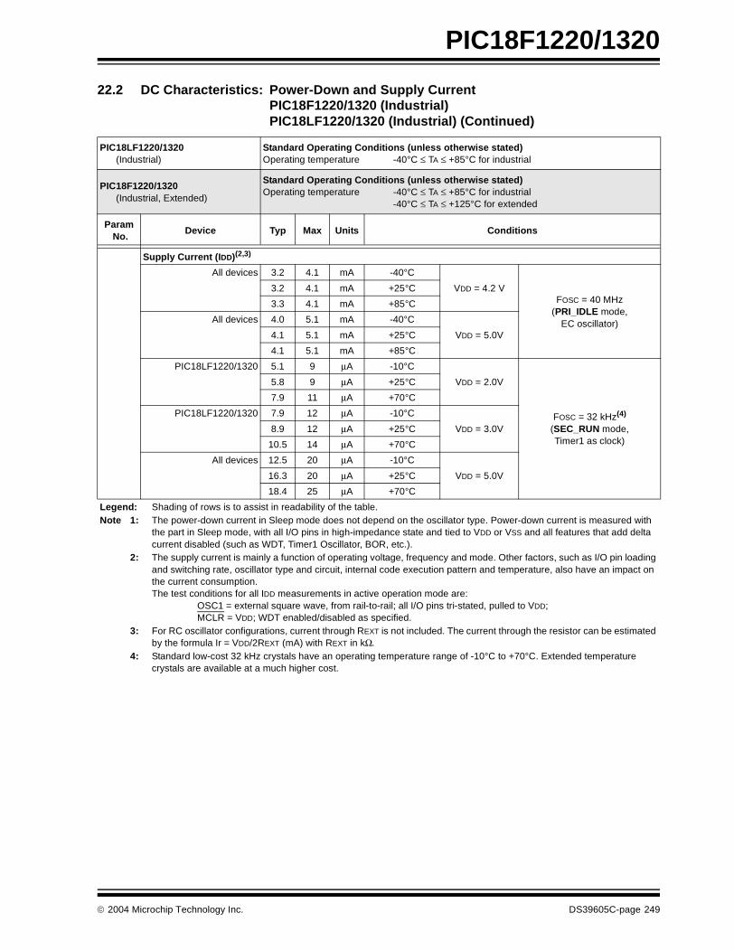
PIC18F1220/1320
Supply Current (IDD)(2,3)
All devices 3.2 4.1 mA -40°C
FOSC = 40 MHz(PRI_IDLE mode,
EC oscillator)
3.2 4.1 mA +25°C VDD = 4.2 V
3.3 4.1 mA +85°C
All devices 4.0 5.1 mA -40°C
VDD = 5.0V4.1 5.1 mA +25°C
4.1 5.1 mA +85°C
PIC18LF1220/1320 5.1 9 µA -10°C
FOSC = 32 kHz(4)
(SEC_RUN mode, Timer1 as clock)
5.8 9 µA +25°C VDD = 2.0V
7.9 11 µA +70°C
PIC18LF1220/1320 7.9 12 µA -10°C
8.9 12 µA +25°C VDD = 3.0V
10.5 14 µA +70°C
All devices 12.5 20 µA -10°C
VDD = 5.0V16.3 20 µA +25°C
18.4 25 µA +70°C
22.2 DC Characteristics: Power-Down and Supply CurrentPIC18F1220/1320 (Industrial) PIC18LF1220/1320 (Industrial) (Continued)
PIC18LF1220/1320 (Industrial)
Standard Operating Conditions (unless otherwise stated)Operating temperature -40°C ≤ TA ≤ +85°C for industrial
PIC18F1220/1320 (Industrial, Extended)
Standard Operating Conditions (unless otherwise stated)Operating temperature -40°C ≤ TA ≤ +85°C for industrial
-40°C ≤ TA ≤ +125°C for extended
Param No.
Device Typ Max Units Conditions
Legend: Shading of rows is to assist in readability of the table.Note 1: The power-down current in Sleep mode does not depend on the oscillator type. Power-down current is measured with
the part in Sleep mode, with all I/O pins in high-impedance state and tied to VDD or VSS and all features that add delta current disabled (such as WDT, Timer1 Oscillator, BOR, etc.).
2: The supply current is mainly a function of operating voltage, frequency and mode. Other factors, such as I/O pin loading and switching rate, oscillator type and circuit, internal code execution pattern and temperature, also have an impact on the current consumption.The test conditions for all IDD measurements in active operation mode are:
OSC1 = external square wave, from rail-to-rail; all I/O pins tri-stated, pulled to VDD;MCLR = VDD; WDT enabled/disabled as specified.
3: For RC oscillator configurations, current through REXT is not included. The current through the resistor can be estimated by the formula Ir = VDD/2REXT (mA) with REXT in kΩ.
4: Standard low-cost 32 kHz crystals have an operating temperature range of -10°C to +70°C. Extended temperature crystals are available at a much higher cost.
2004 Microchip Technology Inc. DS39605C-page 249
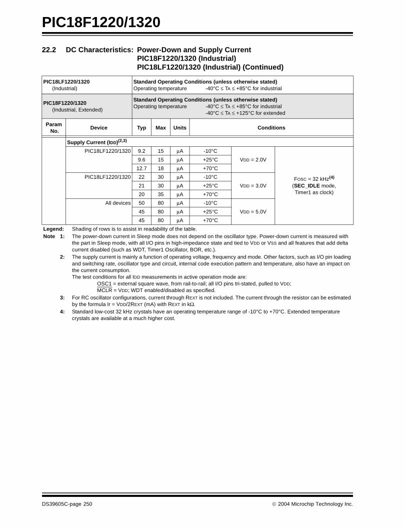
PIC18F1220/1320
Supply Current (IDD)(2,3)
PIC18LF1220/1320 9.2 15 µA -10°C
FOSC = 32 kHz(4)
(SEC_IDLE mode, Timer1 as clock)
9.6 15 µA +25°C VDD = 2.0V
12.7 18 µA +70°C
PIC18LF1220/1320 22 30 µA -10°C
21 30 µA +25°C VDD = 3.0V
20 35 µA +70°C
All devices 50 80 µA -10°C
VDD = 5.0V45 80 µA +25°C
45 80 µA +70°C
22.2 DC Characteristics: Power-Down and Supply CurrentPIC18F1220/1320 (Industrial) PIC18LF1220/1320 (Industrial) (Continued)
PIC18LF1220/1320 (Industrial)
Standard Operating Conditions (unless otherwise stated)Operating temperature -40°C ≤ TA ≤ +85°C for industrial
PIC18F1220/1320 (Industrial, Extended)
Standard Operating Conditions (unless otherwise stated)Operating temperature -40°C ≤ TA ≤ +85°C for industrial
-40°C ≤ TA ≤ +125°C for extended
Param No.
Device Typ Max Units Conditions
Legend: Shading of rows is to assist in readability of the table.Note 1: The power-down current in Sleep mode does not depend on the oscillator type. Power-down current is measured with
the part in Sleep mode, with all I/O pins in high-impedance state and tied to VDD or VSS and all features that add delta current disabled (such as WDT, Timer1 Oscillator, BOR, etc.).
2: The supply current is mainly a function of operating voltage, frequency and mode. Other factors, such as I/O pin loading and switching rate, oscillator type and circuit, internal code execution pattern and temperature, also have an impact on the current consumption.The test conditions for all IDD measurements in active operation mode are:
OSC1 = external square wave, from rail-to-rail; all I/O pins tri-stated, pulled to VDD;MCLR = VDD; WDT enabled/disabled as specified.
3: For RC oscillator configurations, current through REXT is not included. The current through the resistor can be estimated by the formula Ir = VDD/2REXT (mA) with REXT in kΩ.
4: Standard low-cost 32 kHz crystals have an operating temperature range of -10°C to +70°C. Extended temperature crystals are available at a much higher cost.
DS39605C-page 250 2004 Microchip Technology Inc.
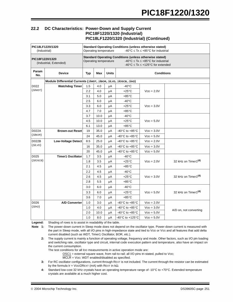
PIC18F1220/1320
Module Differential Currents (∆IWDT, ∆IBOR, ∆ILVD, ∆IOSCB, ∆IAD)
D022(∆IWDT)
Watchdog Timer 1.5 4.0 µA -40°C
2.2 4.0 µA +25°C VDD = 2.0V
3.1 5.0 µA +85°C
2.5 6.0 µA -40°C
3.3 6.0 µA +25°C VDD = 3.0V
4.7 7.0 µA +85°C
3.7 10.0 µA -40°C
4.5 10.0 µA +25°C VDD = 5.0V
6.1 13.0 µA +85°C
D022A(∆IBOR)
Brown-out Reset 19 35.0 µA -40°C to +85°C VDD = 3.0V
24 45.0 µA -40°C to +85°C VDD = 5.0V
D022B(∆ILVD)
Low-Voltage Detect 8.5 25.0 µA -40°C to +85°C VDD = 2.0V
16 35.0 µA -40°C to +85°C VDD = 3.0V
20 45.0 µA -40°C to +85°C VDD = 5.0V
D025(∆IOSCB)
Timer1 Oscillator 1.7 3.5 µA -40°C
1.8 3.5 µA +25°C VDD = 2.0V 32 kHz on Timer1(4)
2.1 4.5 µA +85°C
2.2 4.5 µA -40°C
2.6 4.5 µA +25°C VDD = 3.0V 32 kHz on Timer1(4)
2.8 5.5 µA +85°C
3.0 6.0 µA -40°C
3.3 6.0 µA +25°C VDD = 5.0V 32 kHz on Timer1(4)
3.6 7.0 µA +85°C
D026(∆IAD)
A/D Converter 1.0 3.0 µA -40°C to +85°C VDD = 2.0V
A/D on, not converting1.0 4.0 µA -40°C to +85°C VDD = 3.0V
2.0 10.0 µA -40°C to +85°C VDD = 5.0V
1.0 8.0 µA -40°C to +125°C VDD = 5.0V
22.2 DC Characteristics: Power-Down and Supply CurrentPIC18F1220/1320 (Industrial) PIC18LF1220/1320 (Industrial) (Continued)
PIC18LF1220/1320 (Industrial)
Standard Operating Conditions (unless otherwise stated)Operating temperature -40°C ≤ TA ≤ +85°C for industrial
PIC18F1220/1320 (Industrial, Extended)
Standard Operating Conditions (unless otherwise stated)Operating temperature -40°C ≤ TA ≤ +85°C for industrial
-40°C ≤ TA ≤ +125°C for extended
Param No.
Device Typ Max Units Conditions
Legend: Shading of rows is to assist in readability of the table.Note 1: The power-down current in Sleep mode does not depend on the oscillator type. Power-down current is measured with
the part in Sleep mode, with all I/O pins in high-impedance state and tied to VDD or VSS and all features that add delta current disabled (such as WDT, Timer1 Oscillator, BOR, etc.).
2: The supply current is mainly a function of operating voltage, frequency and mode. Other factors, such as I/O pin loading and switching rate, oscillator type and circuit, internal code execution pattern and temperature, also have an impact on the current consumption.The test conditions for all IDD measurements in active operation mode are:
OSC1 = external square wave, from rail-to-rail; all I/O pins tri-stated, pulled to VDD;MCLR = VDD; WDT enabled/disabled as specified.
3: For RC oscillator configurations, current through REXT is not included. The current through the resistor can be estimated by the formula Ir = VDD/2REXT (mA) with REXT in kΩ.
4: Standard low-cost 32 kHz crystals have an operating temperature range of -10°C to +70°C. Extended temperature crystals are available at a much higher cost.
2004 Microchip Technology Inc. DS39605C-page 251
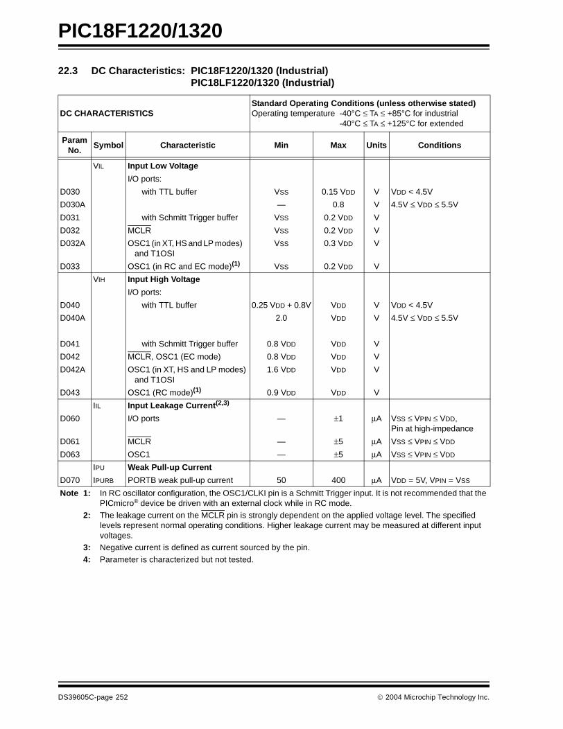
PIC18F1220/1320
22.3 DC Characteristics: PIC18F1220/1320 (Industrial) PIC18LF1220/1320 (Industrial)
DC CHARACTERISTICSStandard Operating Conditions (unless otherwise stated)Operating temperature -40°C ≤ TA ≤ +85°C for industrial
-40°C ≤ TA ≤ +125°C for extended
ParamNo.
Symbol Characteristic Min Max Units Conditions
VIL Input Low Voltage
I/O ports:
D030 with TTL buffer VSS 0.15 VDD V VDD < 4.5V
D030A — 0.8 V 4.5V ≤ VDD ≤ 5.5V
D031 with Schmitt Trigger buffer VSS 0.2 VDD V
D032 MCLR VSS 0.2 VDD V
D032A OSC1 (in XT, HS and LP modes) and T1OSI
VSS 0.3 VDD V
D033 OSC1 (in RC and EC mode)(1) VSS 0.2 VDD V
VIH Input High Voltage
I/O ports:
D040 with TTL buffer 0.25 VDD + 0.8V VDD V VDD < 4.5V
D040A 2.0 VDD V 4.5V ≤ VDD ≤ 5.5V
D041 with Schmitt Trigger buffer 0.8 VDD VDD V
D042 MCLR, OSC1 (EC mode) 0.8 VDD VDD V
D042A OSC1 (in XT, HS and LP modes) and T1OSI
1.6 VDD VDD V
D043 OSC1 (RC mode)(1) 0.9 VDD VDD V
IIL Input Leakage Current(2,3)
D060 I/O ports — ±1 µA VSS ≤ VPIN ≤ VDD, Pin at high-impedance
D061 MCLR — ±5 µA VSS ≤ VPIN ≤ VDD
D063 OSC1 — ±5 µA VSS ≤ VPIN ≤ VDD
IPU Weak Pull-up Current
D070 IPURB PORTB weak pull-up current 50 400 µA VDD = 5V, VPIN = VSS
Note 1: In RC oscillator configuration, the OSC1/CLKI pin is a Schmitt Trigger input. It is not recommended that the PICmicro® device be driven with an external clock while in RC mode.
2: The leakage current on the MCLR pin is strongly dependent on the applied voltage level. The specified levels represent normal operating conditions. Higher leakage current may be measured at different input voltages.
3: Negative current is defined as current sourced by the pin.
4: Parameter is characterized but not tested.
DS39605C-page 252 2004 Microchip Technology Inc.
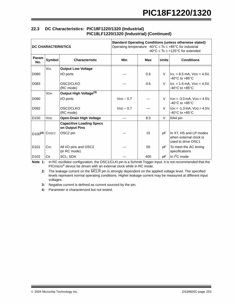
PIC18F1220/1320
VOL Output Low Voltage
D080 I/O ports — 0.6 V IOL = 8.5 mA, VDD = 4.5V, -40°C to +85°C
D083 OSC2/CLKO (RC mode)
— 0.6 V IOL = 1.6 mA, VDD = 4.5V, -40°C to +85°C
VOH Output High Voltage(3)
D090 I/O ports VDD – 0.7 — V IOH = -3.0 mA, VDD = 4.5V, -40°C to +85°C
D092 OSC2/CLKO (RC mode)
VDD – 0.7 — V IOH = -1.3 mA, VDD = 4.5V, -40°C to +85°C
D150 VOD Open-Drain High Voltage — 8.5 V RA4 pin
Capacitive Loading Specson Output Pins
D100(4) COSC2 OSC2 pin — 15 pF In XT, HS and LP modes when external clock is used to drive OSC1
D101 CIO All I/O pins and OSC2 (in RC mode)
— 50 pF To meet the AC timing specifications
D102 CB SCL, SDA — 400 pF In I2C mode
22.3 DC Characteristics: PIC18F1220/1320 (Industrial) PIC18LF1220/1320 (Industrial) (Continued)
DC CHARACTERISTICSStandard Operating Conditions (unless otherwise stated)Operating temperature -40°C ≤ TA ≤ +85°C for industrial
-40°C ≤ TA ≤ +125°C for extended
ParamNo.
Symbol Characteristic Min Max Units Conditions
Note 1: In RC oscillator configuration, the OSC1/CLKI pin is a Schmitt Trigger input. It is not recommended that the PICmicro® device be driven with an external clock while in RC mode.
2: The leakage current on the MCLR pin is strongly dependent on the applied voltage level. The specified levels represent normal operating conditions. Higher leakage current may be measured at different input voltages.
3: Negative current is defined as current sourced by the pin.4: Parameter is characterized but not tested.
2004 Microchip Technology Inc. DS39605C-page 253
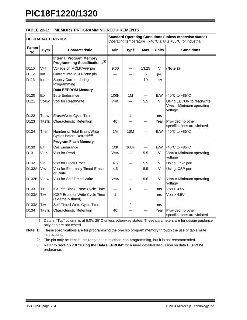
PIC18F1220/1320
TABLE 22-1: MEMORY PROGRAMMING REQUIREMENTS
DC CHARACTERISTICSStandard Operating Conditions (unless otherwise stated)Operating temperature -40°C ≤ TA ≤ +85°C for industrial
ParamNo.
Sym Characteristic Min Typ† Max Units Conditions
Internal Program Memory Programming Specifications(1)
D110 VPP Voltage on MCLR/VPP pin 9.00 — 13.25 V (Note 2)
D112 IPP Current into MCLR/VPP pin — — 5 µA
D113 IDDP Supply Current during Programming
— — 10 mA
Data EEPROM Memory
D120 ED Byte Endurance 100K 1M — E/W -40°C to +85°CD121 VDRW VDD for Read/Write VMIN — 5.5 V Using EECON to read/write
VMIN = Minimum operating voltage
D122 TDEW Erase/Write Cycle Time — 4 — ms
D123 TRETD Characteristic Retention 40 — — Year Provided no other specifications are violated
D124 TREF Number of Total Erase/Write Cycles before Refresh(3)
1M 10M — E/W -40°C to +85°C
Program Flash Memory
D130 EP Cell Endurance 10K 100K — E/W -40°C to +85°CD131 VPR VDD for Read VMIN — 5.5 V VMIN = Minimum operating
voltage
D132 VIE VDD for Block Erase 4.5 — 5.5 V Using ICSP port
D132A VIW VDD for Externally Timed Erase or Write
4.5 — 5.5 V Using ICSP port
D132B VPEW VDD for Self-Timed Write VMIN — 5.5 V VMIN = Minimum operating voltage
D133 TIE ICSP™ Block Erase Cycle Time — 4 — ms VDD > 4.5V
D133A TIW ICSP Erase or Write Cycle Time (externally timed)
1 — — ms VDD > 4.5V
D133A TIW Self-Timed Write Cycle Time — 2 — ms
D134 TRETD Characteristic Retention 40 — — Year Provided no other specifications are violated
† Data in “Typ” column is at 5.0V, 25°C unless otherwise stated. These parameters are for design guidance only and are not tested.
Note 1: These specifications are for programming the on-chip program memory through the use of table write instructions.
2: The pin may be kept in this range at times other than programming, but it is not recommended.3: Refer to Section 7.8 “Using the Data EEPROM” for a more detailed discussion on data EEPROM
endurance.
DS39605C-page 254 2004 Microchip Technology Inc.

PIC18F1220/1320
FIGURE 22-4: LOW-VOLTAGE DETECT CHARACTERISTICS
VLVD
LVDIF
VDD
(LVDIF set by hardware)
(LVDIF can be cleared in software)
TABLE 22-2: LOW-VOLTAGE DETECT CHARACTERISTICSPIC18LF1220/1320 (Industrial)
Standard Operating Conditions (unless otherwise stated)Operating temperature -40°C ≤ TA ≤ +85°C for industrial
PIC18F1220/1320 (Industrial, Extended)
Standard Operating Conditions (unless otherwise stated)Operating temperature -40°C ≤ TA ≤ +85°C for industrial
-40°C ≤ TA ≤ +125°C for extended
Param No.
Symbol Characteristic Min Typ† Max Units Conditions
D420D LVD Voltage on VDD Transition High-to-Low Industrial Low Voltage (-10°C to +85°C)
PIC18LF1220/1320 LVDL<3:0> = 0000 N/A N/A N/A V Reserved
LVDL<3:0> = 0001 N/A N/A N/A V Reserved
LVDL<3:0> = 0010 2.08 2.26 2.44 V
LVDL<3:0> = 0011 2.26 2.45 2.65 V
LVDL<3:0> = 0100 2.35 2.55 2.76 V
LVDL<3:0> = 0101 2.55 2.77 2.99 V
LVDL<3:0> = 0110 2.64 2.87 3.10 V
LVDL<3:0> = 0111 2.82 3.07 3.31 V
LVDL<3:0> = 1000 3.09 3.36 3.63 V
LVDL<3:0> = 1001 3.29 3.57 3.86 V
LVDL<3:0> = 1010 3.38 3.67 3.96 V
LVDL<3:0> = 1011 3.56 3.87 4.18 V
LVDL<3:0> = 1100 3.75 4.07 4.40 V
LVDL<3:0> = 1101 3.93 4.28 4.62 V
LVDL<3:0> = 1110 4.23 4.60 4.96 V
Legend: Shading of rows is to assist in readability of the table.† Production tested at TAMB = 25°C. Specifications over temperature limits ensured by characterization.
2004 Microchip Technology Inc. DS39605C-page 255
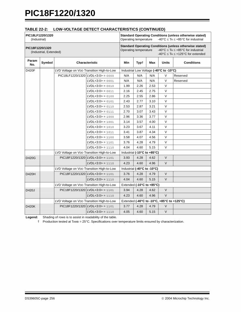
PIC18F1220/1320
D420F LVD Voltage on VDD Transition High-to-Low Industrial Low Voltage (-40°C to -10°C)
PIC18LF1220/1320 LVDL<3:0> = 0000 N/A N/A N/A V Reserved
LVDL<3:0> = 0001 N/A N/A N/A V Reserved
LVDL<3:0> = 0010 1.99 2.26 2.53 V
LVDL<3:0> = 0011 2.16 2.45 2.75 V
LVDL<3:0> = 0100 2.25 2.55 2.86 V
LVDL<3:0> = 0101 2.43 2.77 3.10 V
LVDL<3:0> = 0110 2.53 2.87 3.21 V
LVDL<3:0> = 0111 2.70 3.07 3.43 V
LVDL<3:0> = 1000 2.96 3.36 3.77 V
LVDL<3:0> = 1001 3.14 3.57 4.00 V
LVDL<3:0> = 1010 3.23 3.67 4.11 V
LVDL<3:0> = 1011 3.41 3.87 4.34 V
LVDL<3:0> = 1100 3.58 4.07 4.56 V
LVDL<3:0> = 1101 3.76 4.28 4.79 V
LVDL<3:0> = 1110 4.04 4.60 5.15 V
LVD Voltage on VDD Transition High-to-Low Industrial (-10°C to +85°C)
D420G PIC18F1220/1320 LVDL<3:0> = 1101 3.93 4.28 4.62 V
LVDL<3:0> = 1110 4.23 4.60 4.96 V
LVD Voltage on VDD Transition High-to-Low Industrial (-40°C to -10°C)
D420H PIC18F1220/1320 LVDL<3:0> = 1101 3.76 4.28 4.79 V
LVDL<3:0> = 1110 4.04 4.60 5.15 V
LVD Voltage on VDD Transition High-to-Low Extended (-10°C to +85°C)
D420J PIC18F1220/1320 LVDL<3:0> = 1101 3.94 4.28 4.62 V
LVDL<3:0> = 1110 4.23 4.60 4.96 V
LVD Voltage on VDD Transition High-to-Low Extended (-40°C to -10°C, +85°C to +125°C)
D420K PIC18F1220/1320 LVDL<3:0> = 1101 3.77 4.28 4.79 V
LVDL<3:0> = 1110 4.05 4.60 5.15 V
TABLE 22-2: LOW-VOLTAGE DETECT CHARACTERISTICS (CONTINUED)PIC18LF1220/1320 (Industrial)
Standard Operating Conditions (unless otherwise stated)Operating temperature -40°C ≤ TA ≤ +85°C for industrial
PIC18F1220/1320 (Industrial, Extended)
Standard Operating Conditions (unless otherwise stated)Operating temperature -40°C ≤ TA ≤ +85°C for industrial
-40°C ≤ TA ≤ +125°C for extended
Param No.
Symbol Characteristic Min Typ† Max Units Conditions
Legend: Shading of rows is to assist in readability of the table.† Production tested at TAMB = 25°C. Specifications over temperature limits ensured by characterization.
DS39605C-page 256 2004 Microchip Technology Inc.

PIC18F1220/1320
22.4 AC (Timing) Characteristics
22.4.1 TIMING PARAMETER SYMBOLOGY
The timing parameter symbols have been createdfollowing one of the following formats:
1. TppS2ppS 3. TCC:ST (I2C specifications only)2. TppS 4. Ts (I2C specifications only)T
F Frequency T TimeLowercase letters (pp) and their meanings:pp
cc CCP1 osc OSC1ck CLKO rd RDcs CS rw RD or WR
di SDI sc SCKdo SDO ss SSdt Data in t0 T0CKI
io I/O port t1 T13CKImc MCLR wr WR
Uppercase letters and their meanings:
SF Fall P PeriodH High R Rise
I Invalid (High-Impedance) V ValidL Low Z High-Impedance
I2C only
AA output access High HighBUF Bus free Low Low
TCC:ST (I2C specifications only)
CCHD Hold SU Setup
ST
DAT DATA input hold STO Stop conditionSTA Start condition
2004 Microchip Technology Inc. DS39605C-page 257

PIC18F1220/1320
DS39605C-page 258 2004 Microchip Technology Inc.
22.4.2 TIMING CONDITIONS
The temperature and voltages specified in Table 22-3apply to all timing specifications unless otherwisenoted. Figure 22-5 specifies the load conditions for thetiming specifications.
TABLE 22-3: TEMPERATURE AND VOLTAGE SPECIFICATIONS – AC
FIGURE 22-5: LOAD CONDITIONS FOR DEVICE TIMING SPECIFICATIONS
AC CHARACTERISTICS
Standard Operating Conditions (unless otherwise stated)Operating temperature -40°C ≤ TA ≤ +85°C for industrial
-40°C ≤ TA ≤ +125°C for extendedOperating voltage VDD range as described in DC spec Section 22.1 and Section 22.3. LF parts operate for industrial temperatures only.
VDD/2
CL
RL
pin
Pin
VSS
VSS
CL
RL = 464Ω
CL = 50 pF for all pins except OSC2/CLKO
Load Condition 1 Load Condition 2
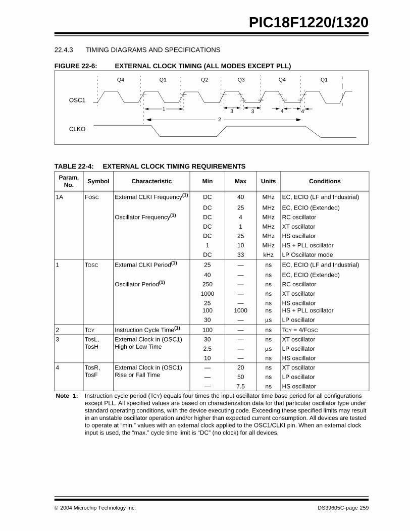
PIC18F1220/1320
22.4.3 TIMING DIAGRAMS AND SPECIFICATIONS
FIGURE 22-6: EXTERNAL CLOCK TIMING (ALL MODES EXCEPT PLL)
TABLE 22-4: EXTERNAL CLOCK TIMING REQUIREMENTS
OSC1
CLKO
Q4 Q1 Q2 Q3 Q4 Q1
1
2
3 3 4 4
Param.No.
Symbol Characteristic Min Max Units Conditions
1A FOSC External CLKI Frequency(1) DC 40 MHz EC, ECIO (LF and Industrial)
DC 25 MHz EC, ECIO (Extended)
Oscillator Frequency(1) DC 4 MHz RC oscillator
DC 1 MHz XT oscillator
DC 25 MHz HS oscillator
1 10 MHz HS + PLL oscillator
DC 33 kHz LP Oscillator mode
1 TOSC External CLKI Period(1) 25 — ns EC, ECIO (LF and Industrial)
40 — ns EC, ECIO (Extended)
Oscillator Period(1) 250 — ns RC oscillator
1000 — ns XT oscillator
25100
—1000
nsns
HS oscillator HS + PLL oscillator
30 — µs LP oscillator
2 TCY Instruction Cycle Time(1) 100 — ns TCY = 4/FOSC
3 TosL,TosH
External Clock in (OSC1) High or Low Time
30 — ns XT oscillator
2.5 — µs LP oscillator
10 — ns HS oscillator
4 TosR,TosF
External Clock in (OSC1) Rise or Fall Time
— 20 ns XT oscillator
— 50 ns LP oscillator
— 7.5 ns HS oscillator
Note 1: Instruction cycle period (TCY) equals four times the input oscillator time base period for all configurations except PLL. All specified values are based on characterization data for that particular oscillator type under standard operating conditions, with the device executing code. Exceeding these specified limits may result in an unstable oscillator operation and/or higher than expected current consumption. All devices are tested to operate at “min.” values with an external clock applied to the OSC1/CLKI pin. When an external clock input is used, the “max.” cycle time limit is “DC” (no clock) for all devices.
2004 Microchip Technology Inc. DS39605C-page 259

PIC18F1220/1320
TABLE 22-5: PLL CLOCK TIMING SPECIFICATIONS, HS/HSPLL MODE (VDD = 4.2V TO 5.5V)
Param No.
Sym Characteristic Min Typ† Max Units Conditions
F10 FOSC Oscillator Frequency Range 4 — 10 MHz HS and HSPLL mode only
F11 FSYS On-Chip VCO System Frequency 16 — 40 MHz HSPLL mode only
F12 TPLL PLL Start-up Time (Lock Time) — — 2 ms HSPLL mode only
F13 ∆CLK CLKO Stability (Jitter) -2 — +2 % HSPLL mode only
† Data in “Typ” column is at 5V, 25°C unless otherwise stated. These parameters are for design guidance only and are not tested.
TABLE 22-6: INTERNAL RC ACCURACY: PIC18F1220/1320 (INDUSTRIAL)PIC18LF1220/1320 (INDUSTRIAL)
PIC18LF1220/1320 (Industrial)
Standard Operating Conditions (unless otherwise stated)Operating temperature -40°C ≤ TA ≤ +85°C for industrial
PIC18F1220/1320 (Industrial)
Standard Operating Conditions (unless otherwise stated)Operating temperature -40°C ≤ TA ≤ +85°C for industrial
-40°C ≤ TA ≤ +125°C for extended
ParamNo.
Device Min Typ Max Units Conditions
INTOSC Accuracy @ Freq = 8 MHz, 4 MHz, 2 MHz, 1 MHz, 500 kHz, 250 kHz, 125 kHz(1)
PIC18LF1220/1320 -2 +/-1 2 % +25°C VDD = 2.7-3.3V
-5 — 5 % -10°C to +85°C VDD = 2.7-3.3V
-10 — 10 % -40°C to +85°C VDD = 2.7-3.3V
PIC18F1220/1320 -2 +/-1 2 % +25°C VDD = 4.5-5.5V
-5 — 5 % -10°C to +85°C VDD = 4.5-5.5V
-10 — 10 % -40°C to +85°C VDD = 4.5-5.5V
INTRC Accuracy @ Freq = 31 kHz(2)
PIC18LF1220/1320 26.562 — 35.938 kHz -40°C to +85°C VDD = 2.7-3.3V
PIC18F1220/1320 26.562 — 35.938 kHz -40°C to +85°C VDD = 4.5-5.5V
Legend: Shading of rows is to assist in readability of the table.
Note 1: Frequency calibrated at 25°C. OSCTUNE register can be used to compensate for temperature and VDD drift.
2: INTRC frequency after calibration.
3: Change of INTRC frequency as VDD changes.
DS39605C-page 260 2004 Microchip Technology Inc.

PIC18F1220/1320
FIGURE 22-7: CLKO AND I/O TIMING
TABLE 22-7: CLKO AND I/O TIMING REQUIREMENTS
Note: Refer to Figure 22-5 for load conditions.
OSC1
CLKO
I/O pin(Input)
I/O pin(Output)
Q4 Q1 Q2 Q3
10
1314
17
20, 21
19 18
15
11
12
16
Old Value New Value
Param. No.
Symbol Characteristic Min Typ Max Units Conditions
10 TosH2ckL OSC1↑ to CLKO↓ — 75 200 ns (Note 1)
11 TosH2ckH OSC1↑ to CLKO↑ — 75 200 ns (Note 1)
12 TckR CLKO Rise Time — 35 100 ns (Note 1)
13 TckF CLKO Fall Time — 35 100 ns (Note 1)
14 TckL2ioV CLKO↓ to Port Out Valid — — 0.5 TCY + 20 ns (Note 1)
15 TioV2ckH Port In Valid before CLKO↑ 0.25 TCY + 25 — — ns (Note 1)
16 TckH2ioI Port In Hold after CLKO↑ 0 — — ns (Note 1)
17 TosH2ioV OSC1↑ (Q1 cycle) to Port Out Valid — 50 150 ns
18 TosH2ioI OSC1↑ (Q2 cycle) to Port Input Invalid (I/O in hold time)
PIC18F1X20 100 — — ns
18A PIC18LF1X20 200 — — ns
19 TioV2osH Port Input Valid to OSC1↑ (I/O in setup time)
0 — — ns
20 TioR Port Output Rise Time PIC18F1X20 — 10 25 ns
20A PIC18LF1X20 — — 60 ns
21 TioF Port Output Fall Time PIC18F1X20 — 10 25 ns
21A PIC18LF1X20 — — 60 ns
Note 1: Measurements are taken in RC mode, where CLKO output is 4 x TOSC.
2004 Microchip Technology Inc. DS39605C-page 261
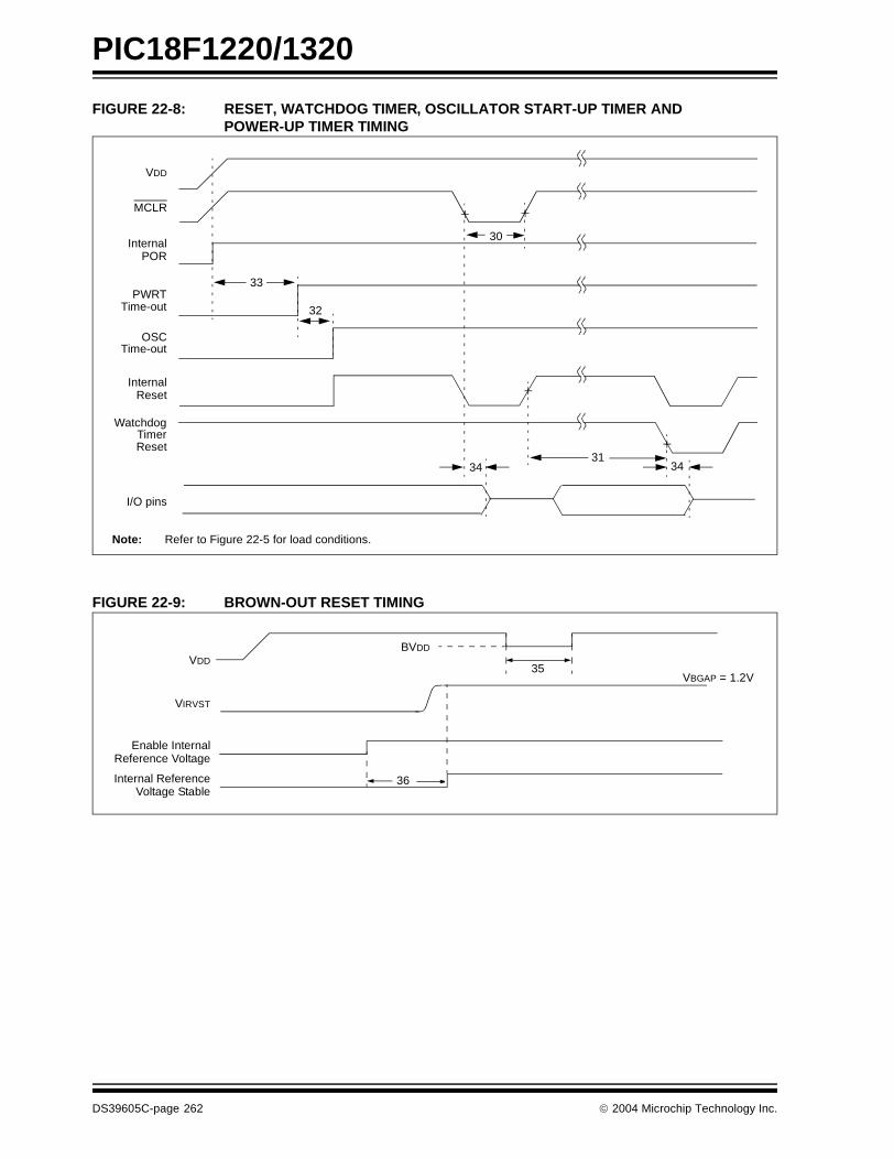
PIC18F1220/1320
FIGURE 22-8: RESET, WATCHDOG TIMER, OSCILLATOR START-UP TIMER AND POWER-UP TIMER TIMING
FIGURE 22-9: BROWN-OUT RESET TIMING
VDD
MCLR
InternalPOR
PWRTTime-out
OSCTime-out
InternalReset
WatchdogTimerReset
33
32
30
3134
I/O pins
34
Note: Refer to Figure 22-5 for load conditions.
VDDBVDD
35VBGAP = 1.2V
VIRVST
Enable Internal
Internal Reference 36
Reference Voltage
Voltage Stable
DS39605C-page 262 2004 Microchip Technology Inc.
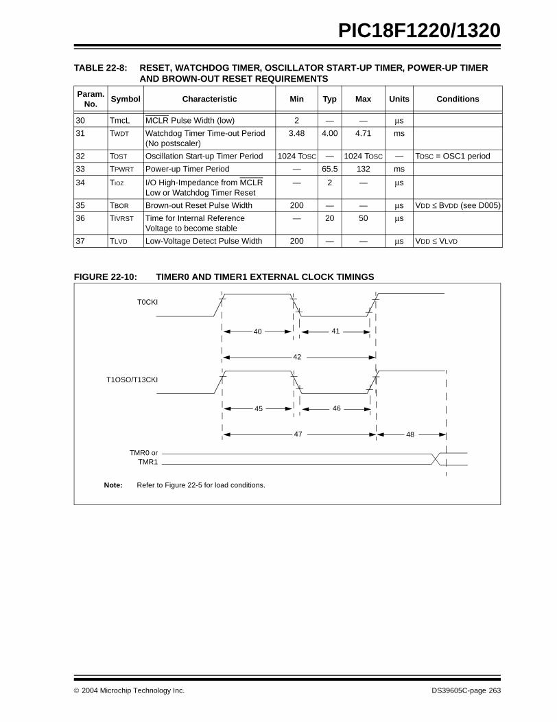
PIC18F1220/1320
TABLE 22-8: RESET, WATCHDOG TIMER, OSCILLATOR START-UP TIMER, POWER-UP TIMER AND BROWN-OUT RESET REQUIREMENTS
FIGURE 22-10: TIMER0 AND TIMER1 EXTERNAL CLOCK TIMINGS
Param. No.
Symbol Characteristic Min Typ Max Units Conditions
30 TmcL MCLR Pulse Width (low) 2 — — µs
31 TWDT Watchdog Timer Time-out Period (No postscaler)
3.48 4.00 4.71 ms
32 TOST Oscillation Start-up Timer Period 1024 TOSC — 1024 TOSC — TOSC = OSC1 period
33 TPWRT Power-up Timer Period — 65.5 132 ms
34 TIOZ I/O High-Impedance from MCLR Low or Watchdog Timer Reset
— 2 — µs
35 TBOR Brown-out Reset Pulse Width 200 — — µs VDD ≤ BVDD (see D005)
36 TIVRST Time for Internal Reference Voltage to become stable
— 20 50 µs
37 TLVD Low-Voltage Detect Pulse Width 200 — — µs VDD ≤ VLVD
Note: Refer to Figure 22-5 for load conditions.
46
47
45
48
41
42
40
T0CKI
T1OSO/T13CKI
TMR0 orTMR1
2004 Microchip Technology Inc. DS39605C-page 263
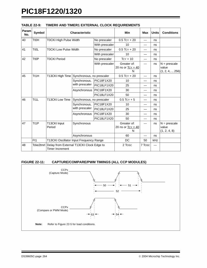
PIC18F1220/1320
TABLE 22-9: TIMER0 AND TIMER1 EXTERNAL CLOCK REQUIREMENTS
FIGURE 22-11: CAPTURE/COMPARE/PWM TIMINGS (ALL CCP MODULES)
ParamNo.
Symbol Characteristic Min Max Units Conditions
40 Tt0H T0CKI High Pulse Width No prescaler 0.5 TCY + 20 — ns
With prescaler 10 — ns
41 Tt0L T0CKI Low Pulse Width No prescaler 0.5 TCY + 20 — ns
With prescaler 10 — ns
42 Tt0P T0CKI Period No prescaler TCY + 10 — ns
With prescaler Greater of:20 ns or TCY + 40
N
— ns N = prescalevalue (1, 2, 4,..., 256)
45 Tt1H T13CKI High Time Synchronous, no prescaler 0.5 TCY + 20 — ns
Synchronous,with prescaler
PIC18F1X20 10 — ns
PIC18LF1X20 25 — ns
Asynchronous PIC18F1X20 30 — ns
PIC18LF1X20 50 — ns
46 Tt1L T13CKI Low Time Synchronous, no prescaler 0.5 TCY + 5 — ns
Synchronous,with prescaler
PIC18F1X20 10 — ns
PIC18LF1X20 25 — ns
Asynchronous PIC18F1X20 30 — ns
PIC18LF1X20 50 — ns
47 Tt1P T13CKI Input Period
Synchronous Greater of:20 ns or TCY + 40
N
— ns N = prescalevalue (1, 2, 4, 8)
Asynchronous 60 — ns
Ft1 T13CKI Oscillator Input Frequency Range DC 50 kHz
48 Tcke2tmrI Delay from External T13CKI Clock Edge to Timer Increment
2 TOSC 7 TOSC —
Note: Refer to Figure 22-5 for load conditions.
CCPx(Capture Mode)
50 51
52
CCPx
53 54
(Compare or PWM Mode)
DS39605C-page 264 2004 Microchip Technology Inc.
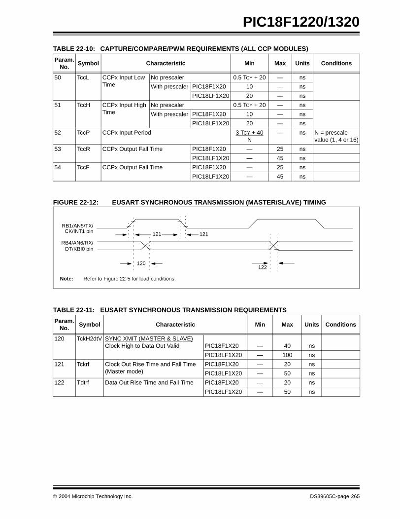
PIC18F1220/1320
TABLE 22-10: CAPTURE/COMPARE/PWM REQUIREMENTS (ALL CCP MODULES)
FIGURE 22-12: EUSART SYNCHRONOUS TRANSMISSION (MASTER/SLAVE) TIMING
TABLE 22-11: EUSART SYNCHRONOUS TRANSMISSION REQUIREMENTS
Param. No.
Symbol Characteristic Min Max Units Conditions
50 TccL CCPx Input Low Time
No prescaler 0.5 TCY + 20 — ns
With prescaler PIC18F1X20 10 — ns
PIC18LF1X20 20 — ns
51 TccH CCPx Input High Time
No prescaler 0.5 TCY + 20 — ns
With prescaler PIC18F1X20 10 — ns
PIC18LF1X20 20 — ns
52 TccP CCPx Input Period 3 TCY + 40N
— ns N = prescale value (1, 4 or 16)
53 TccR CCPx Output Fall Time PIC18F1X20 — 25 ns
PIC18LF1X20 — 45 ns
54 TccF CCPx Output Fall Time PIC18F1X20 — 25 ns
PIC18LF1X20 — 45 ns
121 121
120122
RB1/AN5/TX/
RB4/AN6/RX/DT/KBI0 pin
CK/INT1 pin
Note: Refer to Figure 22-5 for load conditions.
Param. No.
Symbol Characteristic Min Max Units Conditions
120 TckH2dtV SYNC XMIT (MASTER & SLAVE)Clock High to Data Out Valid PIC18F1X20 — 40 ns
PIC18LF1X20 — 100 ns
121 Tckrf Clock Out Rise Time and Fall Time (Master mode)
PIC18F1X20 — 20 ns
PIC18LF1X20 — 50 ns
122 Tdtrf Data Out Rise Time and Fall Time PIC18F1X20 — 20 ns
PIC18LF1X20 — 50 ns
2004 Microchip Technology Inc. DS39605C-page 265

PIC18F1220/1320
FIGURE 22-13: EUSART SYNCHRONOUS RECEIVE (MASTER/SLAVE) TIMING
TABLE 22-12: EUSART SYNCHRONOUS RECEIVE REQUIREMENTS
TABLE 22-13: A/D CONVERTER CHARACTERISTICS: PIC18F1220/1320 (INDUSTRIAL) PIC18LF1220/1320 (INDUSTRIAL)
Param. No.
Symbol Characteristic Min Max Units Conditions
125 TdtV2ckl SYNC RCV (MASTER & SLAVE)Data Hold before CK↓ (DT hold time) 10 — ns
126 TckL2dtl Data Hold after CK↓ (DT hold time) 15 — ns
Param No.
Symbol Characteristic Min Typ Max Units Conditions
A01 NR Resolution — — 10 bit ∆VREF ≥ 3.0V
A03 EIL Integral Linearity Error — — <±1 LSb ∆VREF ≥ 3.0V
A04 EDL Differential Linearity Error — — <±1 LSb ∆VREF ≥ 3.0V
A06 EOFF Offset Error — — <±1 LSb ∆VREF ≥ 3.0V
A07 EGN Gain Error — — <±1 LSb ∆VREF ≥ 3.0V
A10 — Monotonicity guaranteed(2) —
A20 ∆VREF Reference Voltage Range(VREFH – VREFL)
3 — AVDD – AVSS V For 10-bit resolution
A21 VREFH Reference Voltage High AVSS + 3.0V — AVDD + 0.3V V For 10-bit resolution
A22 VREFL Reference Voltage Low AVSS – 0.3V — AVDD – 3.0V V For 10-bit resolution
A25 VAIN Analog Input Voltage VREFL — VREFH V
A28 AVDD Analog Supply Voltage VDD – 0.3 — VDD + 0.3 V
A29 AVSS Analog Supply Voltage VSS – 0.3 — VSS + 0.3 V
A30 ZAIN Recommended Impedance of Analog Voltage Source
— — 2.5 kΩ
A40 IAD A/D ConversionCurrent (VDD)
PIC18F1X20 — 180 — µA Average current consumption when A/D is on (Note 1)
PIC18LF1X20 — 90 — µA
A50 IREF VREF Input Current (Note 3) ——
——
±5±150
µAµA
During VAIN acquisition.During A/D conversion cycle.
Note 1: When A/D is off, it will not consume any current other than minor leakage current. The power-down current specification includes any such leakage from the A/D module.
2: The A/D conversion result never decreases with an increase in the input voltage and has no missing codes.
3: VREFH current is from RA3/AN3/VREF+ pin or AVDD, whichever is selected as the VREFH source.VREFL current is from RA2/AN2/VREF- pin or AVSS, whichever is selected as the VREFL source.
125
126
Note: Refer to Figure 22-5 for load conditions.
RB1/AN5/TX/
RB4/AN6/RX/DT/KBI0 pin
CK/INT1 pin
DS39605C-page 266 2004 Microchip Technology Inc.

PIC18F1220/1320
FIGURE 22-14: A/D CONVERSION TIMING
TABLE 22-14: A/D CONVERSION REQUIREMENTS
131
130
132
BSF ADCON0, GO
Q4
A/D CLK(1)
A/D DATA
ADRES
ADIF
GO
SAMPLE
OLD_DATA
Sampling Stopped
DONE
NEW_DATA
(Note 2)
9 8 7 2 1 0
Note 1: If the A/D clock source is selected as RC, a time of TCY is added before the A/D clock starts. This allows the SLEEP instruction to be executed.
2: This is a minimal RC delay (typically 100 ns), which also disconnects the holding capacitor from the analog input.
. . . . . .
TCY
Param No.
Symbol Characteristic Min Max Units Conditions
130 TAD A/D Clock Period PIC18F1X20 1.6 20(5) µs TOSC based, VREF ≥ 3.0V
PIC18LF1X20 3.0 20(5) µs TOSC based, VREF full range
PIC18F1X20 2.0 6.0 µs A/D RC mode
PIC18LF1X20 3.0 9.0 µs A/D RC mode
131 TCNV Conversion Time (not including acquisition time) (Note 1)
11 12 TAD
132 TACQ Acquisition Time (Note 3) 1510
——
µsµs
-40°C ≤ Temp ≤ +125°C0°C ≤ Temp ≤ +125°C
135 TSWC Switching Time from Convert → Sample — (Note 4)
136 TAMP Amplifier Settling Time (Note 2) 1 — µs This may be used if the “new” input voltage has not changed by more than 1 LSb (i.e., 5 mV @ 5.12V) from the last sampled voltage (as stated on CHOLD).
Note 1: ADRES register may be read on the following TCY cycle.2: See Section 17.0 “10-Bit Analog-to-Digital Converter (A/D) Module” for minimum conditions when input
voltage has changed more than 1 LSb.3: The time for the holding capacitor to acquire the “New” input voltage, when the voltage changes full scale after
the conversion (AVDD to AVSS, or AVSS to AVDD). The source impedance (RS) on the input channels is 50Ω.4: On the next Q4 cycle of the device clock. 5: The time of the A/D clock period is dependent on the device frequency and the TAD clock divider.
2004 Microchip Technology Inc. DS39605C-page 267

PIC18F1220/1320
NOTES:
DS39605C-page 268 2004 Microchip Technology Inc.
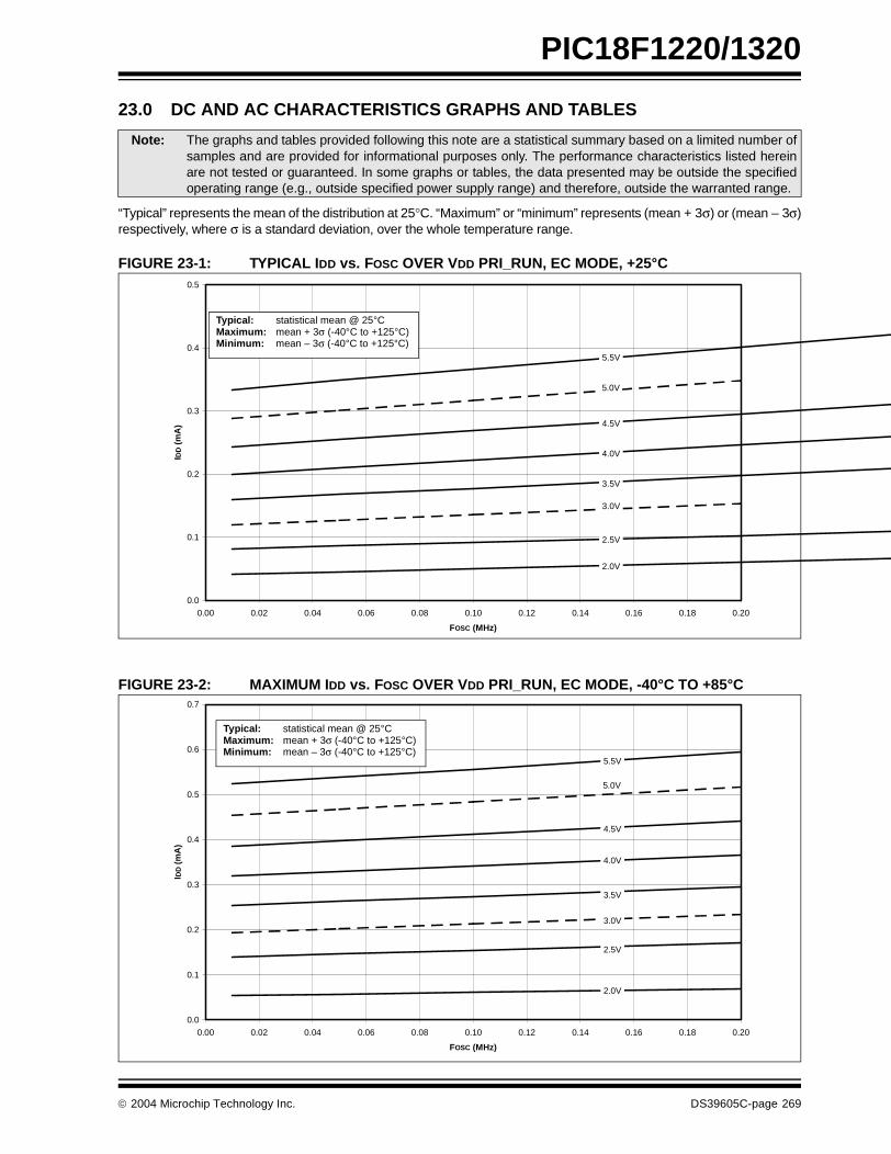
PIC18F1220/1320
23.0 DC AND AC CHARACTERISTICS GRAPHS AND TABLES
“Typical” represents the mean of the distribution at 25°C. “Maximum” or “minimum” represents (mean + 3σ) or (mean – 3σ)respectively, where σ is a standard deviation, over the whole temperature range.
FIGURE 23-1: TYPICAL IDD vs. FOSC OVER VDD PRI_RUN, EC MODE, +25°C
FIGURE 23-2: MAXIMUM IDD vs. FOSC OVER VDD PRI_RUN, EC MODE, -40°C TO +85°C
Note: The graphs and tables provided following this note are a statistical summary based on a limited number ofsamples and are provided for informational purposes only. The performance characteristics listed hereinare not tested or guaranteed. In some graphs or tables, the data presented may be outside the specifiedoperating range (e.g., outside specified power supply range) and therefore, outside the warranted range.
0.0
0.1
0.2
0.3
0.4
0.5
0.00 0.02 0.04 0.06 0.08 0.10 0.12 0.14 0.16 0.18 0.20
FOSC (MHz)
IDD
(m
A)
5.0V
5.5V
4.0V
4.5V
3.0V
3.5V
2.0V
2.5V
Typical: statistical mean @ 25°CMaximum: mean + 3σ (-40°C to +125°C) Minimum: mean – 3σ (-40°C to +125°C)
0.0
0.1
0.2
0.3
0.4
0.5
0.6
0.7
0.00 0.02 0.04 0.06 0.08 0.10 0.12 0.14 0.16 0.18 0.20
FOSC (MHz)
IDD
(m
A)
5.0V
5.5V
4.0V
4.5V
3.0V
3.5V
2.0V
2.5V
Typical: statistical mean @ 25°CMaximum: mean + 3σ (-40°C to +125°C) Minimum: mean – 3σ (-40°C to +125°C)
2004 Microchip Technology Inc. DS39605C-page 269

PIC18F1220/1320
FIGURE 23-3: MAXIMUM IDD vs. FOSC OVER VDD PRI_RUN, EC MODE, -40°C TO +125°C
FIGURE 23-4: TYPICAL IDD vs. FOSC OVER VDD PRI_RUN, EC MODE, +25°C
0.0
0.1
0.2
0.3
0.4
0.5
0.6
0.7
0.00 0.02 0.04 0.06 0.08 0.10 0.12 0.14 0.16 0.18 0.20
FOSC (MHz)
IDD
(m
A)
5.0V
5.5V
4.0V
4.5V
3.0V
3.5V
2.0V
2.5V
Typical: statistical mean @ 25°CMaximum: mean + 3σ (-40°C to +125°C) Minimum: mean – 3σ (-40°C to +125°C)
0.0
0.2
0.4
0.6
0.8
1.0
1.2
1.4
1.6
1.8
2.0
1.0 1.5 2.0 2.5 3.0 3.5 4.0
FOSC (MHz)
IDD
(m
A)
5.0V
5.5V
4.0V
4.5V
3.0V
3.5V
2.0V
2.5V
Typical: statistical mean @ 25°CMaximum: mean + 3σ (-40°C to +125°C) Minimum: mean – 3σ (-40°C to +125°C)
DS39605C-page 270 2004 Microchip Technology Inc.
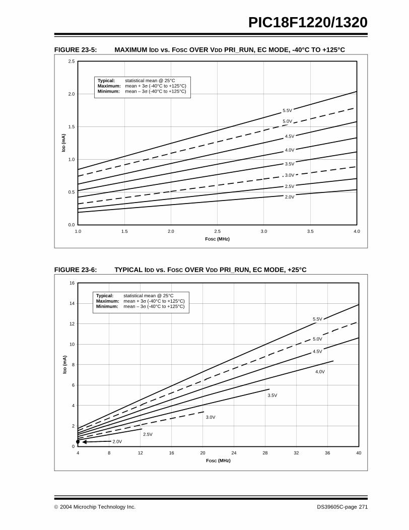
PIC18F1220/1320
FIGURE 23-5: MAXIMUM IDD vs. FOSC OVER VDD PRI_RUN, EC MODE, -40°C TO +125°C
FIGURE 23-6: TYPICAL IDD vs. FOSC OVER VDD PRI_RUN, EC MODE, +25°C
0.0
0.5
1.0
1.5
2.0
2.5
1.0 1.5 2.0 2.5 3.0 3.5 4.0
FOSC (MHz)
IDD
(m
A)
5.0V
5.5V
4.0V
4.5V
3.0V
3.5V
2.0V
2.5V
Typical: statistical mean @ 25°CMaximum: mean + 3σ (-40°C to +125°C) Minimum: mean – 3σ (-40°C to +125°C)
0
2
4
6
8
10
12
14
16
4 8 12 16 20 24 28 32 36 40
FOSC (MHz)
IDD
(m
A)
5.0V
5.5V
4.0V
4.5V
3.0V
3.5V
2.0V
2.5V
Typical: statistical mean @ 25°CMaximum: mean + 3σ (-40°C to +125°C) Minimum: mean – 3σ (-40°C to +125°C)
2004 Microchip Technology Inc. DS39605C-page 271
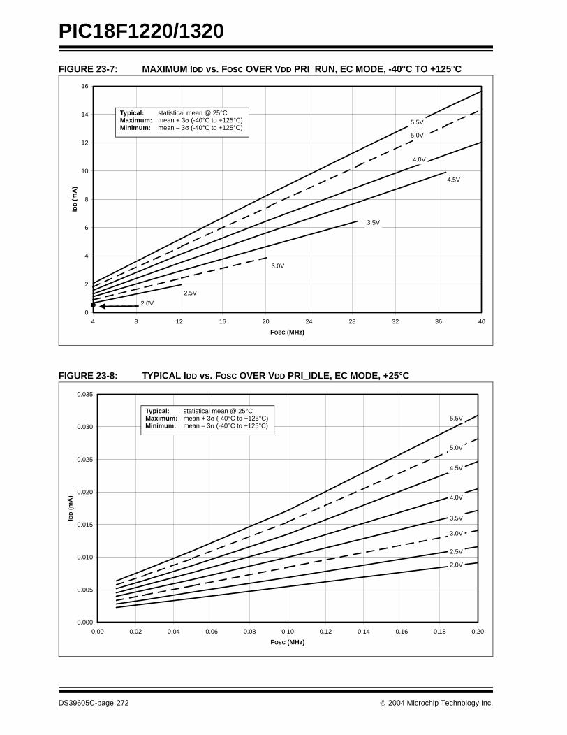
PIC18F1220/1320
FIGURE 23-7: MAXIMUM IDD vs. FOSC OVER VDD PRI_RUN, EC MODE, -40°C TO +125°C
FIGURE 23-8: TYPICAL IDD vs. FOSC OVER VDD PRI_IDLE, EC MODE, +25°C
0
2
4
6
8
10
12
14
16
4 8 12 16 20 24 28 32 36 40
FOSC (MHz)
IDD
(m
A)
5.0V
5.5V
4.0V
4.5V
3.0V
3.5V
2.0V
2.5V
Typical: statistical mean @ 25°CMaximum: mean + 3σ (-40°C to +125°C) Minimum: mean – 3σ (-40°C to +125°C)
0.000
0.005
0.010
0.015
0.020
0.025
0.030
0.035
0.00 0.02 0.04 0.06 0.08 0.10 0.12 0.14 0.16 0.18 0.20
FOSC (MHz)
IDD
(m
A) 4.0V
4.5V
3.0V
3.5V
2.0V
2.5V
5.0V
5.5VTypical: statistical mean @ 25°CMaximum: mean + 3σ (-40°C to +125°C) Minimum: mean – 3σ (-40°C to +125°C)
DS39605C-page 272 2004 Microchip Technology Inc.
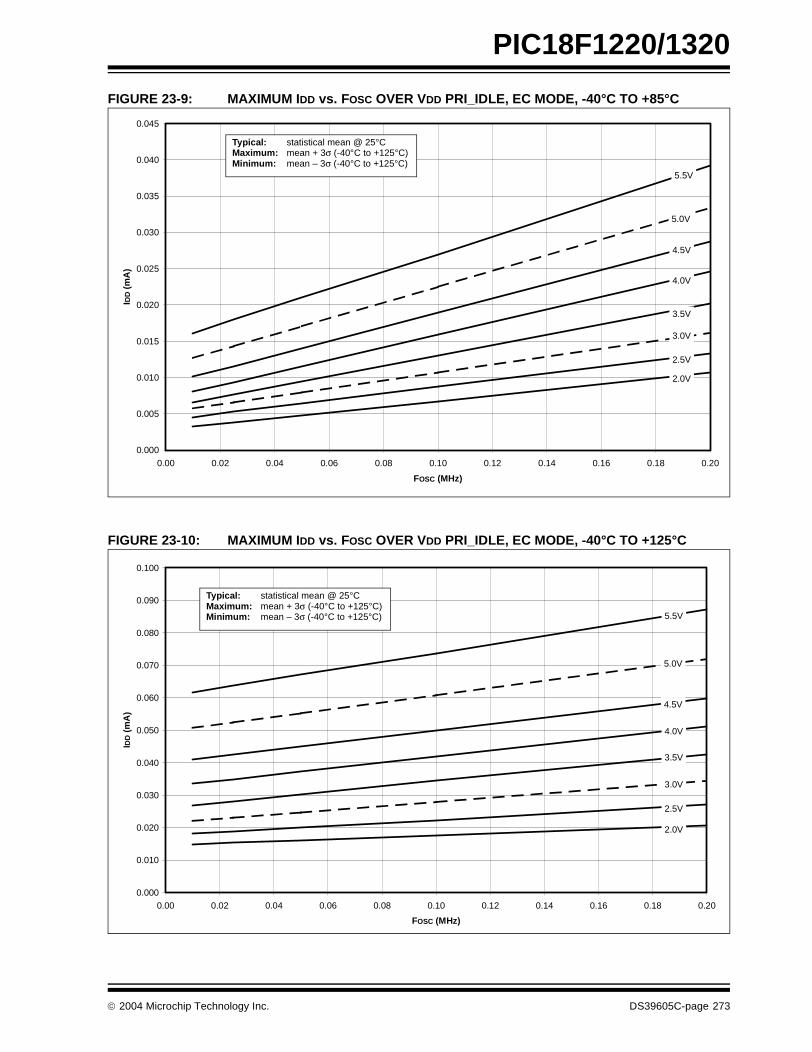
PIC18F1220/1320
FIGURE 23-9: MAXIMUM IDD vs. FOSC OVER VDD PRI_IDLE, EC MODE, -40°C TO +85°C
FIGURE 23-10: MAXIMUM IDD vs. FOSC OVER VDD PRI_IDLE, EC MODE, -40°C TO +125°C
0.000
0.005
0.010
0.015
0.020
0.025
0.030
0.035
0.040
0.045
0.00 0.02 0.04 0.06 0.08 0.10 0.12 0.14 0.16 0.18 0.20
FOSC (MHz)
IDD
(m
A)
4.0V
4.5V
3.0V
3.5V
2.0V
2.5V
5.0V
5.5V
Typical: statistical mean @ 25°CMaximum: mean + 3σ (-40°C to +125°C) Minimum: mean – 3σ (-40°C to +125°C)
0.000
0.010
0.020
0.030
0.040
0.050
0.060
0.070
0.080
0.090
0.100
0.00 0.02 0.04 0.06 0.08 0.10 0.12 0.14 0.16 0.18 0.20
FOSC (MHz)
IDD
(m
A)
4.0V
4.5V
3.0V
3.5V
2.0V
2.5V
5.0V
5.5V
Typical: statistical mean @ 25°CMaximum: mean + 3σ (-40°C to +125°C) Minimum: mean – 3σ (-40°C to +125°C)
2004 Microchip Technology Inc. DS39605C-page 273

PIC18F1220/1320
FIGURE 23-11: TYPICAL IDD vs. FOSC OVER VDD PRI_IDLE, EC MODE, +25°C
FIGURE 23-12: MAXIMUM IDD vs. FOSC OVER VDD PRI_IDLE, EC MODE, -40°C TO +125°C
Typical I vs F over V PRI_IDLE, EC mode, +25°C
0
100
200
300
400
500
600
1.0 1.5 2.0 2.5 3.0 3.5 4.0
FOSC (MHz)
IDD
(µA
)
4.0V
4.5V
3.0V
3.5V
2.0V
2.5V
5.0V
5.5V
Typical: statistical mean @ 25°CMaximum: mean + 3σ (-40°C to +125°C) Minimum: mean – 3σ (-40°C to +125°C)
0
100
200
300
400
500
600
1.0 1.5 2.0 2.5 3.0 3.5 4.0
FOSC (MHz)
IDD
(µA
) 4.0V
4.5V
3.0V
3.5V
2.0V
2.5V
5.0V
5.5VTypical: statistical mean @ 25°CMaximum: mean + 3σ (-40°C to +125°C) Minimum: mean – 3σ (-40°C to +125°C)
DS39605C-page 274 2004 Microchip Technology Inc.

PIC18F1220/1320
FIGURE 23-13: TYPICAL IDD vs. FOSC OVER VDD PRI_IDLE, EC MODE, +25°C
FIGURE 23-14: MAXIMUM IDD vs. FOSC OVER VDD PRI_IDLE, EC MODE, -40°C TO +125°C
0.0
0.5
1.0
1.5
2.0
2.5
3.0
3.5
4.0
4.5
5.0
5.5
6.0
4 8 12 16 20 24 28 32 36 40
FOSC (MHz)
IDD
(m
A)
4.0V
4.5V
3.0V
3.5V
2.0V
2.5V
5.0V
5.5V
Typical: statistical mean @ 25°CMaximum: mean + 3σ (-40°C to +125°C) Minimum: mean – 3σ (-40°C to +125°C)
0.0
0.5
1.0
1.5
2.0
2.5
3.0
3.5
4.0
4.5
5.0
5.5
6.0
4 8 12 16 20 24 28 32 36 40
FOSC (MHz)
IDD
(m
A) 4.0V
4.5V
3.0V
3.5V
2.0V
2.5V
5.0V
5.5V
Typical: statistical mean @ 25°CMaximum: mean + 3σ (-40°C to +125°C) Minimum: mean – 3σ (-40°C to +125°C)
2004 Microchip Technology Inc. DS39605C-page 275
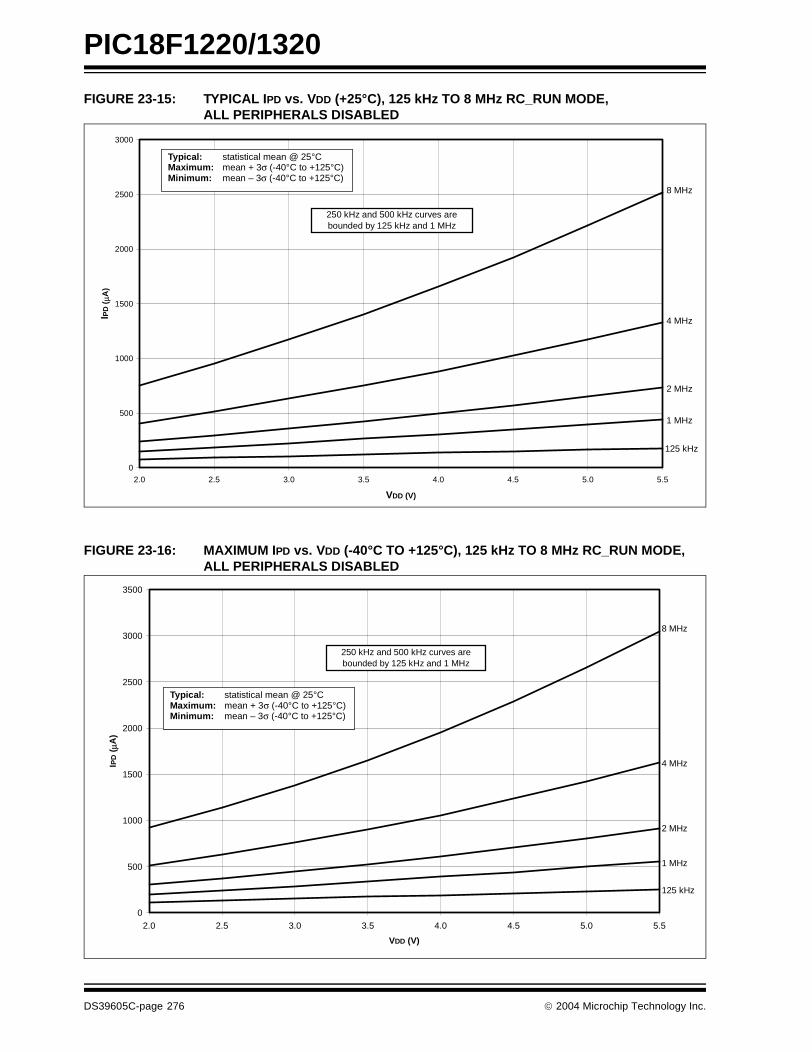
PIC18F1220/1320
FIGURE 23-15: TYPICAL IPD vs. VDD (+25°C), 125 kHz TO 8 MHz RC_RUN MODE, ALL PERIPHERALS DISABLED
FIGURE 23-16: MAXIMUM IPD vs. VDD (-40°C TO +125°C), 125 kHz TO 8 MHz RC_RUN MODE, ALL PERIPHERALS DISABLED
0
500
1000
1500
2000
2500
3000
2.0 2.5 3.0 3.5 4.0 4.5 5.0 5.5
VDD (V)
IPD
(µA
)
8 MHz
125 kHz
4 MHz
2 MHz
1 MHz
250 kHz and 500 kHz curves are bounded by 125 kHz and 1 MHz
curves.
Typical: statistical mean @ 25°CMaximum: mean + 3σ (-40°C to +125°C) Minimum: mean – 3σ (-40°C to +125°C)
0
500
1000
1500
2000
2500
3000
3500
2.0 2.5 3.0 3.5 4.0 4.5 5.0 5.5
VDD (V)
IPD
(µA
)
8 MHz
125 kHz
4 MHz
2 MHz
1 MHz
250 kHz and 500 kHz curves are bounded by 125 kHz and 1 MHz
curves.
Typical: statistical mean @ 25°CMaximum: mean + 3σ (-40°C to +125°C) Minimum: mean – 3σ (-40°C to +125°C)
DS39605C-page 276 2004 Microchip Technology Inc.

PIC18F1220/1320
FIGURE 23-17: TYPICAL AND MAXIMUM IPD vs. VDD (-40°C TO +125°C), 31.25 kHz RC_RUN MODE,ALL PERIPHERALS DISABLED
FIGURE 23-18: TYPICAL IPD vs. VDD (+25°C), 125 kHz TO 8 MHz RC_IDLE MODE, ALL PERIPHERALS DISABLED
1
10
100
2.0 2.5 3.0 3.5 4.0 4.5 5.0 5.5
VDD (V)
IPD
(µA
)
Typ (+25°C)
Max (+85°C)
Max (+125°C)
Typical: statistical mean @ 25°CMaximum: mean + 3σ (-40°C to +125°C) Minimum: mean – 3σ (-40°C to +125°C)
100
150
200
250
300
350
400
450
500
550
600
650
700
750
800
2.0 2.5 3.0 3.5 4.0 4.5 5.0 5.5
VDD (V)
IPD
(µA
)
8 MHz
125 kHz
4 MHz
2 MHz1 MHz
250 kHz and 500 kHz curves are bounded by 125 kHz and 1 MHz
curves.
Typical: statistical mean @ 25°CMaximum: mean + 3σ (-40°C to +125°C) Minimum: mean – 3σ (-40°C to +125°C)
2004 Microchip Technology Inc. DS39605C-page 277

PIC18F1220/1320
FIGURE 23-19: MAXIMUM IPD vs. VDD (-40°C TO +125°C), 125 kHz TO 8 MHz RC_IDLE MODE, ALL PERIPHERALS DISABLED
FIGURE 23-20: TYPICAL AND MAXIMUM IPD vs. VDD (-40°C TO +125°C), 31.25 kHz RC_IDLE MODE,ALL PERIPHERALS DISABLED
100
150
200
250
300
350
400
450
500
550
600
650
700
750
800
2.0 2.5 3.0 3.5 4.0 4.5 5.0 5.5
VDD (V)
IPD
(µA
)
8 MHz
125 kHz
4 MHz
2 MHz1 MHz
250 kHz and 500 kHz curves are bounded by 125 kHz and 1 MHz
curves.
Typical: statistical mean @ 25°CMaximum: mean + 3σ (-40°C to +125°C) Minimum: mean – 3σ (-40°C to +125°C)
1
10
100
2.0 2.5 3.0 3.5 4.0 4.5 5.0 5.5
VDD (V)
IPD
(µA
)
Typ (+25°C)
Max (+85°C)
Max (+125°C)
Typical: statistical mean @ 25°CMaximum: mean + 3σ (-40°C to +125°C) Minimum: mean – 3σ (-40°C to +125°C)
DS39605C-page 278 2004 Microchip Technology Inc.

PIC18F1220/1320
FIGURE 23-21: IPD SEC_RUN MODE, -10°C TO +70°C, 32.768 kHz XTAL, 2 x 22 pF, ALL PERIPHERALS DISABLED
FIGURE 23-22: IPD SEC_IDLE MODE, -10°C TO +70°C, 32.768 kHz, 2 x 22 pF, ALL PERIPHERALS DISABLED
0
10
20
30
40
50
60
70
80
2.0 2.5 3.0 3.5 4.0 4.5 5.0 5.5
VDD (V)
IPD
(µA
)
Typ (+25°C)
Max (+70°C)
Typical: statistical mean @ 25°CMaximum: mean + 3σ (-40°C to +125°C) Minimum: mean – 3σ (-40°C to +125°C)
0
2
4
6
8
10
12
14
16
18
20
2.0 2.5 3.0 3.5 4.0 4.5 5.0 5.5
VDD (V)
IPD
(µA
)
Typ (+25°C)
Max (+70°C)
Typical: statistical mean @ 25°CMaximum: mean + 3σ (-40°C to +125°C) Minimum: mean – 3σ (-40°C to +125°C)
2004 Microchip Technology Inc. DS39605C-page 279
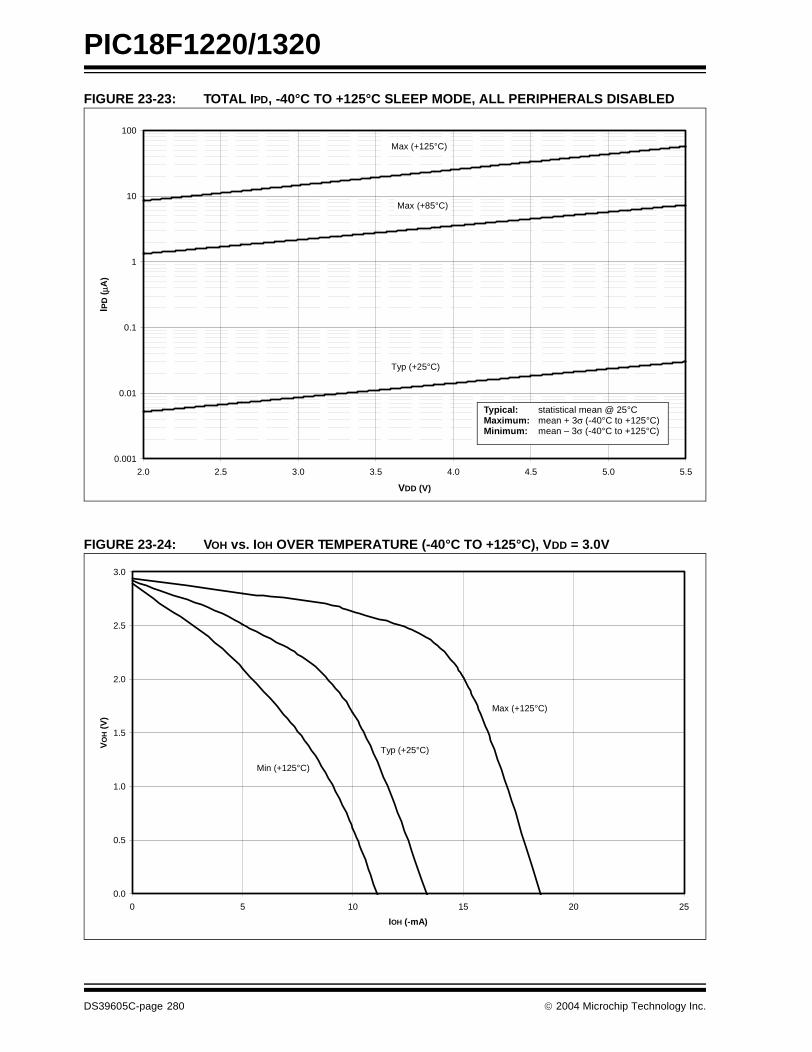
PIC18F1220/1320
FIGURE 23-23: TOTAL IPD, -40°C TO +125°C SLEEP MODE, ALL PERIPHERALS DISABLED
FIGURE 23-24: VOH vs. IOH OVER TEMPERATURE (-40°C TO +125°C), VDD = 3.0V
0.001
0.01
0.1
1
10
100
2.0 2.5 3.0 3.5 4.0 4.5 5.0 5.5
VDD (V)
IPD
(µA
)
Max (+85°C)
Max (+125°C)
Typ (+25°C)
Typical: statistical mean @ 25°CMaximum: mean + 3σ (-40°C to +125°C) Minimum: mean – 3σ (-40°C to +125°C)
0.0
0.5
1.0
1.5
2.0
2.5
3.0
0 5 10 15 20 25
IOH (-mA)
VO
H (
V)
Max (+125°C)
Min (+125°C)
Typ (+25°C)
DS39605C-page 280 2004 Microchip Technology Inc.

PIC18F1220/1320
FIGURE 23-25: VOH vs. IOH OVER TEMPERATURE (-40°C TO +125°C), VDD = 5.0V
FIGURE 23-26: VOL vs. IOL OVER TEMPERATURE (-40°C TO +125°C), VDD = 3.0V
0.0
0.5
1.0
1.5
2.0
2.5
3.0
3.5
4.0
4.5
5.0
0 5 10 15 20 25
IOH (-mA)
VO
H (
V)
Max (+125°C)
Min (+125°C)
Typ (+25°C)
V vs I over Temp (-40°C to +125°C) V = 3.0V
0.0
0.5
1.0
1.5
2.0
2.5
3.0
0 5 10 15 20 25
IOL (-mA)
VO
L (
V)
Max (+125°C)
Max (+85°C)
Typ (+25°C)
Min (+125°C)
2004 Microchip Technology Inc. DS39605C-page 281

PIC18F1220/1320
FIGURE 23-27: VOL vs. IOL OVER TEMPERATURE (-40°C TO +125°C), VDD = 5.0V
FIGURE 23-28: ∆IPD TIMER1 OSCILLATOR, -10°C TO +70°C SLEEP MODE, TMR1 COUNTER DISABLED
0.0
0.1
0.2
0.3
0.4
0.5
0.6
0.7
0.8
0.9
1.0
0 5 10 15 20 25
IOL (-mA)
VO
L (
V)
Max (+125°C)
Max (+85°C)
Typ (+25°C)
Min (+125°C)
IPD Timer1 Oscillator, -10°C to +70°C SLEEP mode, TMR1 counter disabled
0.0
0.5
1.0
1.5
2.0
2.5
3.0
3.5
4.0
4.5
5.0
2.0 2.5 3.0 3.5 4.0 4.5 5.0 5.5
VDD (V)
IPD
(µA
)
Typ (+25°C)
Max (-10°C to +70°C)
Typical: statistical mean @ 25°CMaximum: mean + 3σ (-40°C to +125°C) Minimum: mean – 3σ (-40°C to +125°C)
DS39605C-page 282 2004 Microchip Technology Inc.
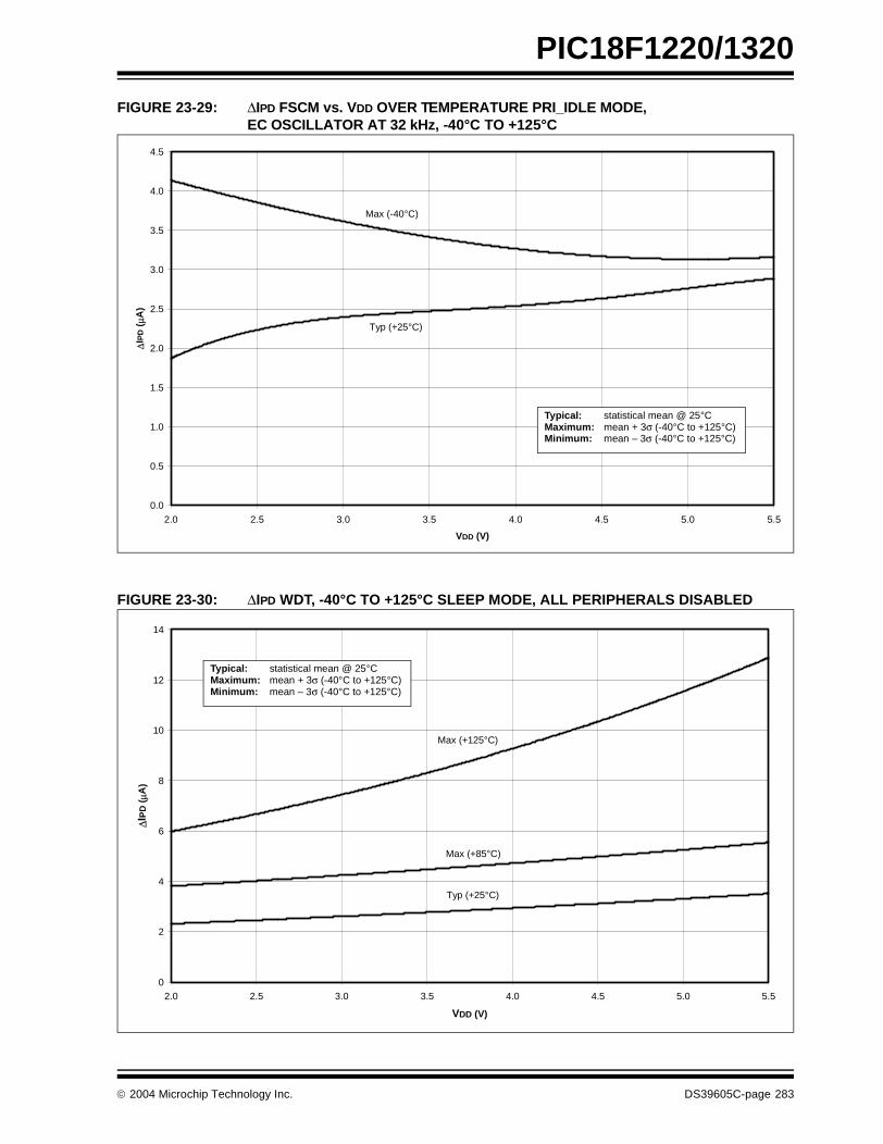
PIC18F1220/1320
FIGURE 23-29: ∆IPD FSCM vs. VDD OVER TEMPERATURE PRI_IDLE MODE, EC OSCILLATOR AT 32 kHz, -40°C TO +125°C
FIGURE 23-30: ∆IPD WDT, -40°C TO +125°C SLEEP MODE, ALL PERIPHERALS DISABLED
0.0
0.5
1.0
1.5
2.0
2.5
3.0
3.5
4.0
4.5
2.0 2.5 3.0 3.5 4.0 4.5 5.0 5.5
VDD (V)
∆IP
D (
µA)
Typ (+25°C)
Max (-40°C)
Typical: statistical mean @ 25°CMaximum: mean + 3σ (-40°C to +125°C) Minimum: mean – 3σ (-40°C to +125°C)
0
2
4
6
8
10
12
14
2.0 2.5 3.0 3.5 4.0 4.5 5.0 5.5
VDD (V)
∆IP
D (
µA)
Typ (+25°C)
Max (+85°C)
Max (+125°C)
Typical: statistical mean @ 25°CMaximum: mean + 3σ (-40°C to +125°C) Minimum: mean – 3σ (-40°C to +125°C)
2004 Microchip Technology Inc. DS39605C-page 283
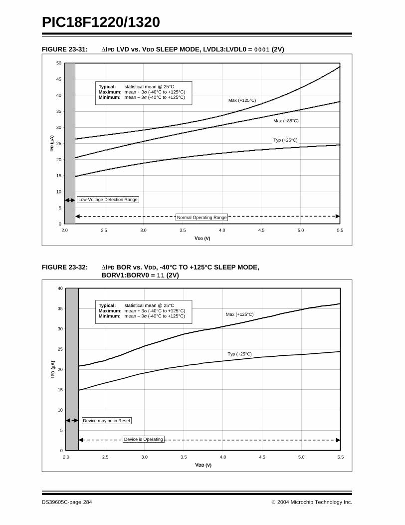
PIC18F1220/1320
FIGURE 23-31: ∆IPD LVD vs. VDD SLEEP MODE, LVDL3:LVDL0 = 0001 (2V)
FIGURE 23-32: ∆IPD BOR vs. VDD, -40°C TO +125°C SLEEP MODE, BORV1:BORV0 = 11 (2V)
0
5
10
15
20
25
30
35
40
45
50
2.0 2.5 3.0 3.5 4.0 4.5 5.0 5.5
VDD (V)
IPD
(µA
)
Typ (+25°C)
Max (+85°C)
Max (+125°C)
Low-Voltage Detection Range
Normal Operating Range
Typical: statistical mean @ 25°CMaximum: mean + 3σ (-40°C to +125°C) Minimum: mean – 3σ (-40°C to +125°C)
0
5
10
15
20
25
30
35
40
2.0 2.5 3.0 3.5 4.0 4.5 5.0 5.5
VDD (V)
IPD
(µA
)
Max (+125°C)
Typ (+25°C)
Device may be in Reset
Device is Operating
Typical: statistical mean @ 25°CMaximum: mean + 3σ (-40°C to +125°C) Minimum: mean – 3σ (-40°C to +125°C)
DS39605C-page 284 2004 Microchip Technology Inc.

PIC18F1220/1320
FIGURE 23-33: ∆IPD A/D, -40°C TO +125°C SLEEP MODE, A/D ENABLED (NOT CONVERTING)
FIGURE 23-34: AVERAGE FOSC vs. VDD FOR VARIOUS R’s EXTERNAL RC MODE, C = 20 pF, TEMPERATURE = +25°C
0.001
0.01
0.1
1
10
2.0 2.5 3.0 3.5 4.0 4.5 5.0 5.5
VDD (V)
IPD
(µA
)
Max (+125°C)
Max (+85°C)
Typ (+25°C)
Typical: statistical mean @ 25°CMaximum: mean + 3σ (-40°C to +125°C) Minimum: mean – 3σ (-40°C to +125°C)
0.0
0.5
1.0
1.5
2.0
2.5
3.0
3.5
4.0
4.5
5.0
2.0 2.5 3.0 3.5 4.0 4.5 5.0 5.5
VDD (V)
Fre
q (
MH
z)
5.1K
10K
33K
100K
Operation above 4 MHz is not recomended
2004 Microchip Technology Inc. DS39605C-page 285
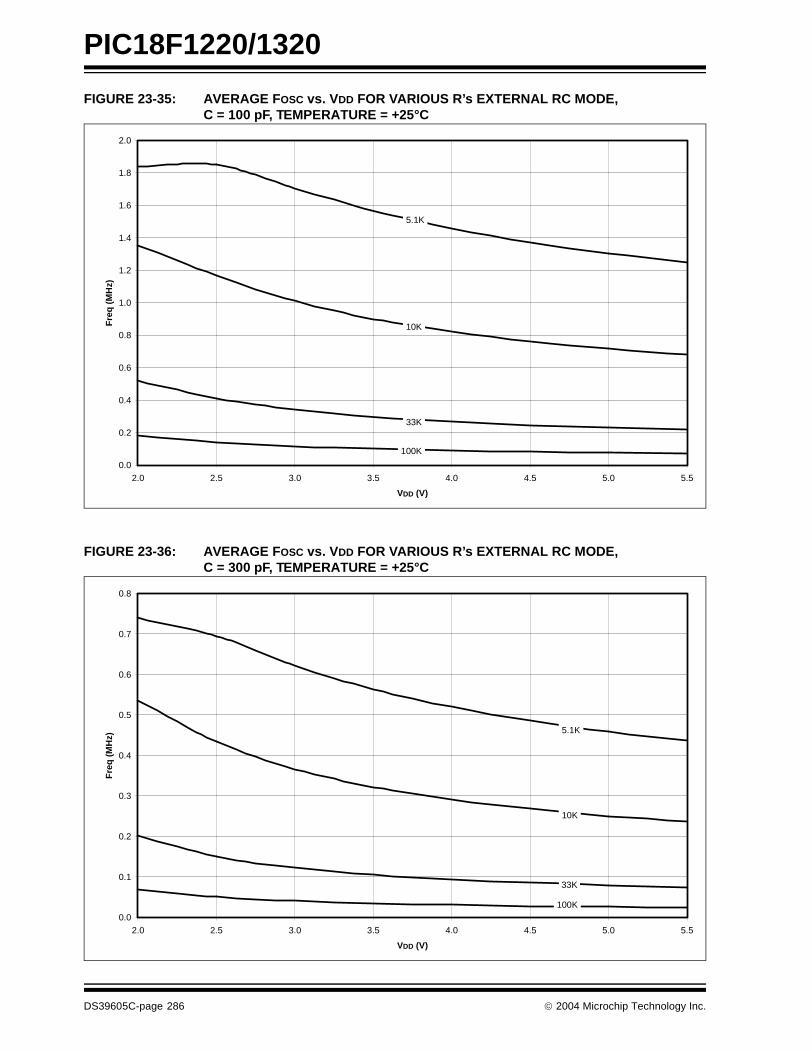
PIC18F1220/1320
FIGURE 23-35: AVERAGE FOSC vs. VDD FOR VARIOUS R’s EXTERNAL RC MODE, C = 100 pF, TEMPERATURE = +25°C
FIGURE 23-36: AVERAGE FOSC vs. VDD FOR VARIOUS R’s EXTERNAL RC MODE, C = 300 pF, TEMPERATURE = +25°C
0.0
0.2
0.4
0.6
0.8
1.0
1.2
1.4
1.6
1.8
2.0
2.0 2.5 3.0 3.5 4.0 4.5 5.0 5.5
VDD (V)
Fre
q (
MH
z)
5.1K
10K
33K
100K
0.0
0.1
0.2
0.3
0.4
0.5
0.6
0.7
0.8
2.0 2.5 3.0 3.5 4.0 4.5 5.0 5.5
VDD (V)
Fre
q (
MH
z)
5.1K
10K
33K
100K
DS39605C-page 286 2004 Microchip Technology Inc.
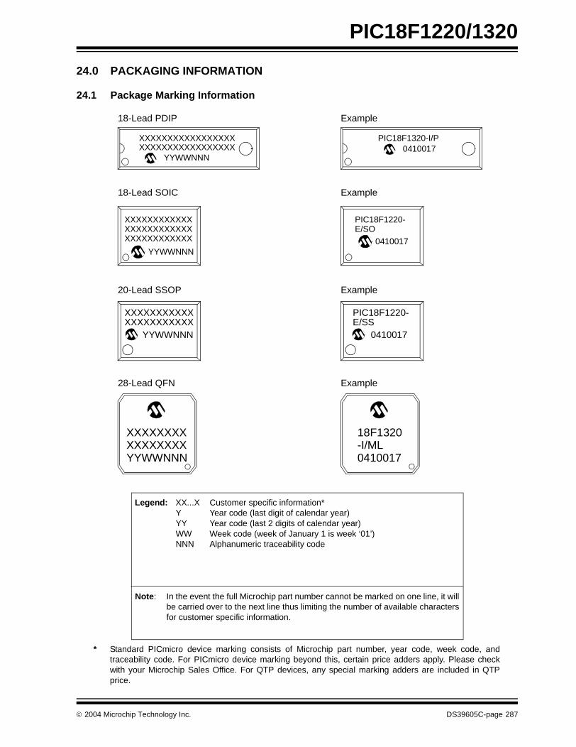
PIC18F1220/1320
24.0 PACKAGING INFORMATION
24.1 Package Marking Information
18-Lead PDIP
XXXXXXXXXXXXXXXXXXXXXXXXXXXXXXXXXX
YYWWNNN
Example
PIC18F1320-I/P0410017
18-Lead SOIC
XXXXXXXXXXXXXXXXXXXXXXXXXXXXXXXXXXXX
YYWWNNN
Example
PIC18F1220-E/SO
0410017
20-Lead SSOP
XXXXXXXXXXXXXXXXXXXXXX
YYWWNNN
Example
PIC18F1220-E/SS
0410017
28-Lead QFN
XXXXXXXXXXXXXXXXYYWWNNN
Example
18F1320-I/ML0410017
Legend: XX...X Customer specific information*Y Year code (last digit of calendar year)YY Year code (last 2 digits of calendar year)WW Week code (week of January 1 is week ‘01’)NNN Alphanumeric traceability code
Note: In the event the full Microchip part number cannot be marked on one line, it willbe carried over to the next line thus limiting the number of available charactersfor customer specific information.
* Standard PICmicro device marking consists of Microchip part number, year code, week code, andtraceability code. For PICmicro device marking beyond this, certain price adders apply. Please checkwith your Microchip Sales Office. For QTP devices, any special marking adders are included in QTPprice.
2004 Microchip Technology Inc. DS39605C-page 287

PIC18F1220/1320
24.2 Package Details
The following sections give the technical details of thepackages.
18-Lead Plastic Dual In-line (P) – 300 mil Body (PDIP)
1510515105βMold Draft Angle Bottom1510515105αMold Draft Angle Top
10.929.407.87.430.370.310eBOverall Row Spacing §0.560.460.36.022.018.014BLower Lead Width1.781.461.14.070.058.045B1Upper Lead Width0.380.290.20.015.012.008cLead Thickness3.433.303.18.135.130.125LTip to Seating Plane
22.9922.8022.61.905.898.890DOverall Length6.606.356.10.260.250.240E1Molded Package Width8.267.947.62.325.313.300EShoulder to Shoulder Width
0.38.015A1Base to Seating Plane3.683.302.92.145.130.115A2Molded Package Thickness4.323.943.56.170.155.140ATop to Seating Plane
2.54.100pPitch1818nNumber of Pins
MAXNOMMINMAXNOMMINDimension LimitsMILLIMETERSINCHES*Units
1
2
D
n
E1
c
eB
β
E
α
p
A2
L
B1
B
A
A1
* Controlling Parameter
Notes:Dimensions D and E1 do not include mold flash or protrusions. Mold flash or protrusions shall not exceed .010” (0.254mm) per side.JEDEC Equivalent: MS-001Drawing No. C04-007
§ Significant Characteristic
DS39605C-page 288 2004 Microchip Technology Inc.

PIC18F1220/1320
18-Lead Plastic Small Outline (SO) – Wide, 300 mil Body (SOIC)
Foot Angle φ 0 4 8 0 4 8
1512015120βMold Draft Angle Bottom1512015120αMold Draft Angle Top
0.510.420.36.020.017.014BLead Width0.300.270.23.012.011.009cLead Thickness
1.270.840.41.050.033.016LFoot Length0.740.500.25.029.020.010hChamfer Distance
11.7311.5311.33.462.454.446DOverall Length7.597.497.39.299.295.291E1Molded Package Width
10.6710.3410.01.420.407.394EOverall Width0.300.200.10.012.008.004A1Standoff §2.392.312.24.094.091.088A2Molded Package Thickness2.642.502.36.104.099.093AOverall Height
1.27.050pPitch1818nNumber of Pins
MAXNOMMINMAXNOMMINDimension LimitsMILLIMETERSINCHES*Units
Lβ
c
φ
h
45°
1
2
D
p
nB
E1
E
α
A2
A1
A
* Controlling Parameter
Notes:Dimensions D and E1 do not include mold flash or protrusions. Mold flash or protrusions shall not exceed .010” (0.254mm) per side.JEDEC Equivalent: MS-013Drawing No. C04-051
§ Significant Characteristic
2004 Microchip Technology Inc. DS39605C-page 289

PIC18F1220/1320
20-Lead Plastic Shrink Small Outline (SS) – 209 mil Body, 5.30 mm (SSOP)
0.38-0.22.015-.009BLead Width
8°4°0°8°4°0°fFoot Angle
0.25-0.09.010-.004cLead Thickness
0.950.750.55.037.030.022LFoot Length
7.507.20.295.289.283.272DOverall Length
5.605.305.00.220.209.197E1Molded Package Width
8.207.807.40.323.307.291EOverall Width
--0.05--.002A1Standoff
1.851.751.65.073.069.065A2Molded Package Thickness
2.00--.079--AOverall Height
0.65.026pPitch
2020nNumber of Pins
MAXNOMMINMAXNOMMINDimension Limits
MILLIMETERS*INCHESUnits
2
1
D
p
n
B
E
E1
L
c
f
A2A
A1
shall not exceed .010" (0.254mm) per side.Dimensions D and E1 do not include mold flash or protrusions. Mold flash or protrusions
Notes:
JEDEC Equivalent: MO-150Drawing No. C04-072
*Controlling Parameter
Revised 11/03/03
DS39605C-page 290 2004 Microchip Technology Inc.
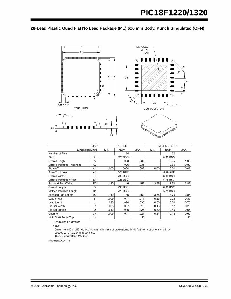
PIC18F1220/1320
28-Lead Plastic Quad Flat No Lead Package (ML) 6x6 mm Body, Punch Singulated (QFN)
Lead Width
*Controlling Parameter
Drawing No. C04-114
Notes:
Mold Draft Angle Top
Dimensions D and E1 do not include mold flash or protrusions. Mold flash or protrusions shall not
exceed .010" (0.254mm) per side.
B
ı α
.009
12°
.011 .014 0.23
12°
0.28 0.35
Pitch
Number of Pins
Overall Width
Standoff
Molded Package Length
Overall Length
Molded Package Width
Molded Package Thickness
Overall Height
MAX
Units
Dimension Limits
A2
A1
E1
D
D1
E
n
p
A
.026
.236 BSC
.000
.226 BSC
INCHES
.026 BSC
MIN
28
NOM MAX
0.65.031
.002 0.00
6.00 BSC
5.75 BSC
MILLIMETERS*
.039
MIN
28
0.65 BSC
NOM
0.80
0.05
1.00
.008 REFBase Thickness A3 0.20 REF
JEDEC equivalent: MO-220
0.85.033
.0004 0.01
.236 BSC
.226 BSC
6.00 BSC
5.75 BSC
Lead Length
Tie Bar Width
L .020 .024 .030 0.50 0.60 0.75
R .005 .007 .010 0.13 0.17 0.23
Tie Bar Length Q .012 .016 .026 0.30 0.40 0.65
Chamfer CH .009 .017 .024 0.24 0.42 0.60
E2
D2
Exposed Pad Width
Exposed Pad Length .140 .146 .152 3.55 3.70 3.85
.140 .146 .152 3.55 3.70 3.85
D
E
E1
n
1
2
D1
AA2
EXPOSED
METAL
PAD
BOTTOM VIEWTOP VIEW
Q
L
R
p
A1
A3
ı
CH X 45°
B
D2
E2
α
2004 Microchip Technology Inc. DS39605C-page 291

PIC18F1220/1320
NOTES:
DS39605C-page 292 2004 Microchip Technology Inc.

PIC18F1220/1320
APPENDIX A: REVISION HISTORY
Revision A (August 2002)
Original data sheet for PIC18F1220/1320 devices.
Revision B (November 2002)
This revision includes significant changes toSection 2.0, Section 3.0 and Section 19.0, as well asupdates to the Electrical Specifications in Section 22.0and includes minor corrections to the data sheet text.
Revision C (May 2004)
This revision includes updates to the Electrical Specifi-cations in Section 22.0, the DC and AC CharacteristicsGraphs and Tables in Section 23.0 and includes minorcorrections to the data sheet text.
APPENDIX B: DEVICE DIFFERENCES
The differences between the devices listed in this datasheet are shown in Table B-1.
TABLE B-1: DEVICE DIFFERENCES
Features PIC18F1220 PIC18F1320
Program Memory (Bytes) 4096 8192
Program Memory (Instructions) 2048 4096
Interrupt Sources 15 15
I/O Ports Ports A, B Ports A, B
Enhanced Capture/Compare/PWM Modules 1 1
10-bit Analog-to-Digital Module 7 input channels 7 input channels
Packages
18-pin SDIP18-pin SOIC20-pin SSOP28-pin QFN
18-pin SDIP18-pin SOIC20-pin SSOP28-pin QFN
2004 Microchip Technology Inc. DS39605C-page 293

PIC18F1220/1320
APPENDIX C: CONVERSION CONSIDERATIONS
This appendix discusses the considerations for con-verting from previous versions of a device to the oneslisted in this data sheet. Typically, these changes aredue to the differences in the process technology used.An example of this type of conversion is from aPIC16C74A to a PIC16C74B.
Not Applicable
APPENDIX D: MIGRATION FROM BASELINE TO ENHANCED DEVICES
This section discusses how to migrate from a baselinedevice (i.e., PIC16C5X) to an enhanced MCU device(i.e., PIC18FXXX).
The following are the list of modifications over thePIC16C5X microcontroller family:
Not Currently Available
DS39605C-page 294 2004 Microchip Technology Inc.
PIC18F1220/1320
APPENDIX E: MIGRATION FROM MID-RANGE TO ENHANCED DEVICES
A detailed discussion of the differences between themid-range MCU devices (i.e., PIC16CXXX) and theenhanced devices (i.e., PIC18FXXX) is provided inAN716, “Migrating Designs from PIC16C74A/74B toPIC18C442”. The changes discussed, while devicespecific, are generally applicable to all mid-range toenhanced device migrations.
This Application Note is available as Literature NumberDS00716.
APPENDIX F: MIGRATION FROM HIGH-END TO ENHANCED DEVICES
A detailed discussion of the migration pathway anddifferences between the high-end MCU devices (i.e.,PIC17CXXX) and the enhanced devices (i.e.,PIC18FXXX) is provided in AN726, “PIC17CXXX toPIC18CXXX Migration”.
This Application Note is available as Literature NumberDS00726.
2004 Microchip Technology Inc. DS39605C-page 295

PIC18F1220/1320
NOTES:
DS39605C-page 296 2004 Microchip Technology Inc.

PIC18F1220/1320
INDEX
AA/D ................................................................................... 155
A/D Converter Interrupt, Configuring ....................... 159Acquisition Requirements ........................................ 160ADCON0 Register .................................................... 155ADCON1 Register .................................................... 155ADCON2 Register .................................................... 155ADRESH Register .................................................... 155ADRESH/ADRESL Registers .................................. 158ADRESL Register .................................................... 155Analog Port Pins, Configuring .................................. 162Associated Registers ............................................... 164Configuring the Module ............................................ 159Conversion Clock (Tad) ........................................... 161Conversion Requirements ....................................... 267Conversion Status (GO/DONE Bit) .......................... 158Conversions ............................................................. 163Converter Characteristics ........................................ 266Operation in Low-Power Modes ............................... 162Selecting, Configuring Automatic
Acquisition Time ............................................... 161Special Event Trigger (CCP) .................................... 117Special Event Trigger (CCP1) .................................. 164Use of the CCP1 Trigger .......................................... 164VREF+ and VREF- References .................................. 160
Absolute Maximum Ratings ............................................. 239AC (Timing) Characteristics ............................................. 257
Conditions ................................................................ 258Load Conditions for Device
Timing Specifications ....................................... 258Parameter Symbology ............................................. 257Temperature and Voltage Specifications ................. 258
ADCON0 Register ............................................................ 155GO/DONE Bit ........................................................... 158
ADCON1 Register ............................................................ 155ADCON2 Register ............................................................ 155ADDLW ............................................................................ 197ADDWF ............................................................................ 197ADDWFC ......................................................................... 198ADRESH Register ............................................................ 155ADRESH/ADRESL Registers ........................................... 158ADRESL Register ............................................................ 155Analog-to-Digital Converter. See A/D.ANDLW ............................................................................ 198ANDWF ............................................................................ 199Assembler
MPASM Assembler .................................................. 233Auto-Wake-up on Sync Break Character ......................... 145
BBC .................................................................................... 199BCF .................................................................................. 200Block Diagrams
A/D ........................................................................... 158Analog Input Model .................................................. 159Capture Mode Operation ......................................... 117Compare Mode Operation ....................................... 118Enhanced PWM ....................................................... 120EUSART Receive .................................................... 143EUSART Transmit ................................................... 141Fail-Safe Clock Monitor ............................................ 182Generic I/O Port Operation ........................................ 87Low-Voltage Detect (LVD) ....................................... 166
Low-Voltage Detect (LVD) with External Input .................................................. 166
MCLR/VPP/RA5 Pin ................................................... 89On-Chip Reset Circuit ................................................ 33OSC1/CLKI/RA7 Pin .................................................. 88OSC2/CLKO/RA6 Pin ................................................ 88PIC18F1220/1320 ....................................................... 7PLL ............................................................................ 12RA3:RA0 Pins ............................................................ 88RA4/T0CKI Pin .......................................................... 88RB0/AN4/INT0 Pin ..................................................... 90RB1/AN5/TX/CK/INT1 Pin ......................................... 91RB2/P1B/INT2 Pin ..................................................... 92RB3/CCP1/P1A Pin ................................................... 93RB4/AN6/RX/DT/KBI0 Pin ......................................... 94RB5/PGM/KBI1 Pin .................................................... 95RB6/PGC/T1OSO/T13CKI/P1C/KBI2 Pin .................. 96RB7/PGD/T1OSI/P1D/KBI3 Pin ................................. 97Reads from Flash Program Memory .......................... 61System Clock ............................................................. 16Table Read Operation ............................................... 57Table Write Operation ................................................ 58Table Writes to Flash Program Memory .................... 63Timer0 in 16-Bit Mode ............................................. 100Timer0 in 8-Bit Mode ............................................... 100Timer1 ..................................................................... 104Timer1 (16-Bit Read/Write Mode) ............................ 104Timer2 ..................................................................... 110Timer3 ..................................................................... 112Timer3 (16-bit Read/Write Mode) ............................ 112WDT ........................................................................ 180
BN .................................................................................... 200BNC ................................................................................. 201BNN ................................................................................. 201BNOV ............................................................................... 202BNZ .................................................................................. 202BOR. See Brown-out Reset.BOV ................................................................................. 205BRA ................................................................................. 203Break Character (12-bit) Transmit and Receive .............. 146Brown-out Reset (BOR) ..............................................34, 171BSF .................................................................................. 203BTFSC ............................................................................. 204BTFSS ............................................................................. 204BTG ................................................................................. 205BZ .................................................................................... 206
CC Compilers
MPLAB C17 ............................................................. 234MPLAB C18 ............................................................. 234MPLAB C30 ............................................................. 234
CALL ................................................................................ 206Capture (CCP Module) .................................................... 116
CCP Pin Configuration ............................................. 116CCPR1H:CCPR1L Registers ................................... 116Software Interrupt .................................................... 116Timer1/Timer3 Mode Selection ................................ 116
Capture, Compare, Timer1 and Timer3Associated Registers ............................................... 118
2004 Microchip Technology Inc. DS39605C-page 297
PIC18F1220/1320
Capture/Compare/PWM (CCP)Capture Mode. See Capture.CCP1 ........................................................................ 116
CCPR1H Register ............................................ 116CCPR1L Register ............................................ 116
Compare Mode. See Compare.Timer Resources ...................................................... 116
Clock Sources .................................................................... 15Selection Using OSCCON Register ........................... 16
Clocking Scheme ............................................................... 45CLRF ................................................................................ 207CLRWDT .......................................................................... 207Code Examples
16 x 16 Signed Multiply Routine ................................. 7216 x 16 Unsigned Multiply Routine ............................. 728 x 8 Signed Multiply Routine ..................................... 718 x 8 Unsigned Multiply Routine ................................. 71Changing Between Capture Prescalers ................... 117Computed GOTO Using an Offset Value ................... 47Data EEPROM Read ................................................. 69Data EEPROM Refresh Routine ................................ 70Data EEPROM Write .................................................. 69Erasing a Flash Program Memory Row ..................... 62Fast Register Stack .................................................... 44How to Clear RAM (Bank 1) Using
Indirect Addressing ............................................ 53Implementing a Real-Time Clock Using
a Timer1 Interrupt Service ............................... 107Initializing PORTA ...................................................... 87Initializing PORTB ...................................................... 90Reading a Flash Program Memory Word ................... 61Saving Status, WREG and
BSR Registers in RAM ....................................... 85Writing to Flash Program Memory ....................... 64–65
Code Protection ............................................................... 171COMF ............................................................................... 208Compare (CCP Module) ................................................... 117
CCP Pin Configuration ............................................. 117CCPR1 Register ....................................................... 117Software Interrupt ..................................................... 117Special Event Trigger ....................................... 113, 117Timer1/Timer3 Mode Selection ................................ 117
Compare (CCP1 Module)Special Event Trigger ............................................... 164
Computed GOTO ............................................................... 47Configuration Bits ............................................................. 171Context Saving During Interrupts ....................................... 85Conversion Considerations .............................................. 294CPFSEQ .......................................................................... 208CPFSGT ........................................................................... 209CPFSLT ........................................................................... 209
DData EEPROM Memory ..................................................... 67
Associated Registers ................................................. 70EEADR Register ........................................................ 67EECON1 Register ...................................................... 67EECON2 Register ...................................................... 67Operation During Code-Protect .................................. 70Protection Against Spurious Write ............................. 69Reading ...................................................................... 69Using .......................................................................... 70Write Verify ................................................................. 69Writing ........................................................................ 69
Data Memory ..................................................................... 47General Purpose Registers ....................................... 47Map for PIC18F1220/1320 Devices ........................... 48Special Function Registers ........................................ 49
DAW ................................................................................ 210DC and AC Characteristics
Graphs and Tables .................................................. 269DC Characteristics ........................................................... 252
Power-Down and Supply Current ............................ 243Supply Voltage ......................................................... 242
DCFSNZ .......................................................................... 211DECF ............................................................................... 210DECFSZ .......................................................................... 211Demonstration Boards
PICDEM 1 ................................................................ 236PICDEM 17 .............................................................. 237PICDEM 18R ........................................................... 237PICDEM 2 Plus ........................................................ 236PICDEM 3 ................................................................ 236PICDEM 4 ................................................................ 236PICDEM LIN ............................................................ 237PICDEM USB .......................................................... 237PICDEM.net Internet/Ethernet ................................. 236
Details on Individual Family Members ................................. 6Development Support ...................................................... 233Device Differences ........................................................... 293Direct Addressing ............................................................... 54
EEffects of Power Managed Modes on
Various Clock Sources .............................................. 18Electrical Characteristics .................................................. 239Enhanced Capture/Compare/PWM (ECCP) .................... 115
Outputs .................................................................... 116PWM Mode. See PWM (ECCP Module).
Enhanced PWM Mode. See PWM (ECCP Module). Enhanced Universal Synchronous Asynchronous
Receiver Transmitter (EUSART) ............................. 131Equations
16 x 16 Signed Multiplication Algorithm ..................... 7216 x 16 Unsigned Multiplication Algorithm ................. 72A/D Minimum Charging Time ................................... 160Acquisition Time ...................................................... 160
Errata ................................................................................... 4EUSART
Asynchronous Mode ................................................ 14012-bit Break Transmit and Receive ................. 146Associated Registers, Receive ........................ 144Associated Registers, Transmit ....................... 142Auto-Wake-up on Sync Break ......................... 145Receiver .......................................................... 143Setting up 9-bit Mode with
Address Detect ........................................ 143Transmitter ....................................................... 140
Baud Rate Generator (BRG) ................................... 135Associated Registers ....................................... 136Auto-Baud Rate Detect .................................... 139Baud Rate Error, Calculating ........................... 135Baud Rates, Asynchronous Modes ................. 136High Baud Rate Select (BRGH Bit) ................. 135Power Managed Mode Operation .................... 135Sampling .......................................................... 135
Serial Port Enable (SPEN Bit) ................................. 131
DS39605C-page 298 2004 Microchip Technology Inc.

PIC18F1220/1320
Synchronous Master Mode ...................................... 148Associated Registers, Reception ..................... 151Associated Registers, Transmit ....................... 149Reception ......................................................... 150Transmission .................................................... 148
Synchronous Slave Mode ........................................ 152Associated Registers, Receive ........................ 153Associated Registers, Transmit ....................... 152Reception ......................................................... 153Transmission .................................................... 152
Evaluation and Programming Tools ................................. 237
FFail-Safe Clock Monitor .................................................... 171
Exiting Operation ..................................................... 183Interrupts in Power Managed Modes ....................... 183POR or Wake from Sleep ........................................ 184WDT During Oscillator Failure ................................. 182
Fail-Safe Clock Monitor (FSCM) ...................................... 182Fast Register Stack ............................................................ 44Firmware Instructions ....................................................... 191Flash Program Memory ...................................................... 57
Associated Registers ................................................. 65Control Registers ....................................................... 58Erase Sequence ........................................................ 62Erasing ....................................................................... 62Operation During Code-Protect ................................. 65Reading ...................................................................... 61Table Latch ................................................................ 60Table Pointer .............................................................. 60
Boundaries Based on Operation ........................ 60Table Pointer Boundaries .......................................... 60Table Reads and Table Writes .................................. 57Write Sequence ......................................................... 63Writing to .................................................................... 63
Unexpected Termination .................................... 65Write Verify ........................................................ 65
GGOTO ............................................................................... 212
HHardware Multiplier ............................................................ 71
Introduction ................................................................ 71Operation ................................................................... 71Performance Comparison .......................................... 71
II/O Ports ............................................................................. 87ID Locations ............................................................. 171, 188INCF ................................................................................. 212INCFSZ ............................................................................ 213In-Circuit Debugger .......................................................... 188In-Circuit Serial Programming (ICSP) ...................... 171, 188Indirect Addressing ............................................................ 54
INDF and FSR Registers ........................................... 53Operation ................................................................... 53
Indirect Addressing Operation ............................................ 54Indirect File Operand .......................................................... 47INFSNZ ............................................................................ 213Initialization Conditions for All Registers ...................... 36–38Instruction Cycle ................................................................. 45Instruction Flow/Pipelining ................................................. 45
Instruction Set .................................................................. 191ADDLW .................................................................... 197ADDWF .................................................................... 197ADDWFC ................................................................. 198ANDLW .................................................................... 198ANDWF .................................................................... 199BC ............................................................................ 199BCF ......................................................................... 200BN ............................................................................ 200BNC ......................................................................... 201BNN ......................................................................... 201BNOV ...................................................................... 202BNZ ......................................................................... 202BOV ......................................................................... 205BRA ......................................................................... 203BSF .......................................................................... 203BTFSC ..................................................................... 204BTFSS ..................................................................... 204BTG ......................................................................... 205BZ ............................................................................ 206CALL ........................................................................ 206CLRF ....................................................................... 207CLRWDT ................................................................. 207COMF ...................................................................... 208CPFSEQ .................................................................. 208CPFSGT .................................................................. 209CPFSLT ................................................................... 209DAW ........................................................................ 210DCFSNZ .................................................................. 211DECF ....................................................................... 210DECFSZ .................................................................. 211General Format ........................................................ 193GOTO ...................................................................... 212INCF ........................................................................ 212INCFSZ .................................................................... 213INFSNZ .................................................................... 213IORLW ..................................................................... 214IORWF ..................................................................... 214LFSR ....................................................................... 215MOVF ...................................................................... 215MOVFF .................................................................... 216MOVLB .................................................................... 216MOVLW ................................................................... 217MOVWF ................................................................... 217MULLW .................................................................... 218MULWF .................................................................... 218NEGF ....................................................................... 219NOP ......................................................................... 219POP ......................................................................... 220PUSH ....................................................................... 220RCALL ..................................................................... 221RESET ..................................................................... 221RETFIE .................................................................... 222RETLW .................................................................... 222RETURN .................................................................. 223RLCF ....................................................................... 223RLNCF ..................................................................... 224RRCF ....................................................................... 224RRNCF .................................................................... 225SETF ....................................................................... 225SLEEP ..................................................................... 226SUBFWB ................................................................. 226SUBLW .................................................................... 227
2004 Microchip Technology Inc. DS39605C-page 299

PIC18F1220/1320
SUBWF .................................................................... 227SUBWFB .................................................................. 228SWAPF .................................................................... 228TBLRD ..................................................................... 229TBLWT ..................................................................... 230TSTFSZ .................................................................... 231XORLW .................................................................... 231XORWF .................................................................... 232Summary Table ........................................................ 194
INTCON RegisterRBIF Bit ...................................................................... 90
INTCON Registers ............................................................. 75Internal Oscillator Block ..................................................... 14
Adjustment ................................................................. 14INTIO Modes .............................................................. 14INTRC Output Frequency .......................................... 14OSCTUNE Register ................................................... 14
Internal RC OscillatorUse with WDT .......................................................... 180
Interrupt Sources .............................................................. 171A/D Conversion Complete ........................................ 159Capture Complete (CCP) ......................................... 116Compare Complete (CCP) ....................................... 117Interrupt-on-Change (RB7:RB4) ................................ 90INTn Pin ..................................................................... 85PORTB, Interrupt-on-Change .................................... 85TMR0 ......................................................................... 85TMR0 Overflow ........................................................ 101TMR1 Overflow ........................................................ 103TMR2 to PR2 Match ................................................. 110TMR2 to PR2 Match (PWM) ............................ 109, 119TMR3 Overflow ................................................ 111, 113
Interrupts ............................................................................ 73Enable Bits
(CCP1IE Bit) .................................................... 116Flag Bits
CCP1 Flag (CCP1IF Bit) .................................. 116CCP1IF Flag (CCP1IF Bit) ............................... 117Interrupt-on-Change (RB7:RB4)
Flag (RBIF Bit) ........................................... 90Logic ........................................................................... 74
INTOSC Frequency Drift .................................................... 30IORLW ............................................................................. 214IORWF ............................................................................. 214IPR Registers ..................................................................... 82
LLFSR ................................................................................ 215Low-Voltage Detect .......................................................... 165
Characteristics ......................................................... 255Effects of a Reset ..................................................... 169Operation ................................................................. 168
Current Consumption ....................................... 169Reference Voltage Set Point ............................ 169
Operation During Sleep ............................................ 169LVD. See Low-Voltage Detect.
MMemory Organization ......................................................... 41
Data Memory .............................................................. 47Program Memory ....................................................... 41
Memory Programming Requirements .............................. 254Migration from Baseline to Enhanced Devices ................ 294Migration from High-End to Enhanced Devices ............... 295
Migration from Mid-Range to Enhanced Devices ................................................... 295
MOVF .............................................................................. 215MOVFF ............................................................................ 216MOVLB ............................................................................ 216MOVLW ........................................................................... 217MOVWF ........................................................................... 217MPLAB ASM30 Assembler, Linker, Librarian .................. 234MPLAB ICD 2 In-Circuit Debugger .................................. 235MPLAB ICE 2000 High-Performance
Universal In-Circuit Emulator ................................... 235MPLAB ICE 4000 High-Performance
Universal In-Circuit Emulator ................................... 235MPLAB Integrated Development
Environment Software ............................................. 233MPLAB PM3 Device Programmer ................................... 235MPLINK Object Linker/MPLIB Object Librarian ............... 234MULLW ............................................................................ 218MULWF ............................................................................ 218
NNEGF ............................................................................... 219New Core Features
Multiple Oscillator Options and Features ..................... 5nanoWatt Technology .................................................. 5
NOP ................................................................................. 219
OOpcode Field Descriptions ............................................... 192OPTION_REG Register
PSA Bit .................................................................... 101T0CS Bit .................................................................. 101T0PS2:T0PS0 Bits ................................................... 101T0SE Bit ................................................................... 101
Oscillator Configuration ...................................................... 11Crystal/Ceramic Resonator ........................................ 11EC .............................................................................. 11ECIO .......................................................................... 11External Clock Input ................................................... 13HS .............................................................................. 11HSPLL ..................................................................11, 12INTIO1 ....................................................................... 11INTIO2 ....................................................................... 11LP .............................................................................. 11RC .........................................................................11, 13RCIO .......................................................................... 11XT .............................................................................. 11
Oscillator Selection .......................................................... 171Oscillator Start-up Timer (OST) ............................18, 34, 171Oscillator Switching ............................................................ 15Oscillator Transitions ......................................................... 18Oscillator, Timer1 ......................................................103, 113Oscillator, Timer3 ............................................................. 111Other Special Features ........................................................ 5
PPackaging ........................................................................ 287
Details ...................................................................... 288Marking Information ................................................. 287
PICkit 1 Flash Starter Kit .................................................. 237PICSTART Plus Development Programmer .................... 236PIE Registers ..................................................................... 80
DS39605C-page 300 2004 Microchip Technology Inc.
PIC18F1220/1320
Pin FunctionsMCLR/VPP/RA5 ............................................................ 8OSC1/CLKI/RA7 .......................................................... 8OSC2/CLKO/RA6 ........................................................ 8RA0/AN0 ...................................................................... 8RA1/AN1/LVDIN .......................................................... 8RA2/AN2/VREF- ............................................................ 8RA3/AN3/VREF+ ........................................................... 8RA4/T0CKI ................................................................... 8RB0/AN4/INT0 ............................................................. 9RB1/AN5/TX/CK/INT1 .................................................. 9RB2/P1B/INT2 ............................................................. 9RB3/CCP1/P1A ............................................................ 9RB4/AN6/RX/DT/KBI0 ................................................. 9RB5/PGM/KBI1 ............................................................ 9RB6/PGC/T1OSO/T13CKI/P1C/KBI2 .......................... 9RB7/PGD/T1OSI/P1D/KBI3 ......................................... 9VDD ............................................................................... 9VSS ............................................................................... 9
Pinout I/O DescriptionsPIC18F1220/1320 ........................................................ 8
PIR Registers ..................................................................... 78PLL Lock Time-out ............................................................. 34Pointer, FSR ....................................................................... 53POP .................................................................................. 220POR. See Power-on Reset.PORTA
Associated Registers ................................................. 89Functions ................................................................... 89LATA Register ............................................................ 87PORTA Register ........................................................ 87TRISA Register .......................................................... 87
PORTBAssociated Registers ................................................. 98Functions ................................................................... 98LATB Register ............................................................ 90PORTB Register ........................................................ 90RB7:RB4 Interrupt-on-Change
Flag (RBIF Bit) ................................................... 90TRISB Register .......................................................... 90
PostscalerTimer2 ...................................................................... 109WDT
Assignment (PSA Bit) ...................................... 101Rate Select (T0PS2:T0PS0 Bits) ..................... 101
Power Managed Modes ..................................................... 19Comparison between Run
and Idle Modes .................................................. 20Entering ...................................................................... 20Idle Modes ................................................................. 21Multiple Sleep Commands ......................................... 20Run Modes ................................................................. 26Selecting .................................................................... 19Sleep Mode ................................................................ 21Summary (table) ........................................................ 19Wake from .................................................................. 28
Power-on Reset (POR) .............................................. 34, 171Power-up Delays ................................................................ 18Power-up Timer (PWRT) .......................................18, 34, 171Prescaler
Capture .................................................................... 117Timer0 ...................................................................... 101
Assignment (PSA Bit) ...................................... 101Rate Select (T0PS2:T0PS0 Bits) ..................... 101
Timer2 ...................................................................... 119
PRO MATE II Universal Device Programmer .................. 235Product Identification System .......................................... 307Program Counter
PCL Register ............................................................. 44PCLATH Register ...................................................... 44PCLATU Register ...................................................... 44
Program MemoryInstructions in ............................................................ 46Interrupt Vector .......................................................... 41Map and Stack for PIC18F1220 ................................ 41Map and Stack for PIC18F1320 ................................ 41Reset Vector .............................................................. 41
Program Verification and Code Protection ...................... 185Associated Registers ............................................... 185Configuration Register ............................................. 188Data EEPROM ......................................................... 188Program Memory ..................................................... 186
Programming, Device Instructions ................................... 191PUSH ............................................................................... 220PUSH and POP Instructions .............................................. 43PWM (CCP Module)
CCPR1H:CCPR1L Registers ................................... 119Duty Cycle ............................................................... 119Example Frequencies/Resolutions .......................... 119Period ...................................................................... 119TMR2 to PR2 Match .........................................109, 119
PWM (ECCP Module) ...................................................... 119Associated Registers ............................................... 130Direction Change in Full-Bridge
Output Mode .................................................... 124Effects of a Reset .................................................... 129Enhanced PWM Auto-Shutdown ............................. 126Full-Bridge Application Example .............................. 124Full-Bridge PWM Output
(Active-High) Diagram ..................................... 123Half-Bridge Output
(Active-High) Diagram ..................................... 122Half-Bridge Output Mode
Applications Example ...................................... 122Operation in Low-Power Modes .............................. 129Output Configurations .............................................. 119Output Relationships (Active-High) .......................... 120Output Relationships (Active-Low) .......................... 121Programmable Dead-Band Delay ............................ 126PWM Direction Change
(Active-High) Diagram ..................................... 125PWM Direction Change at Near 100%
Duty Cycle (Active-High) Diagram ................... 125Setup for PWM Operation ........................................ 129Start-up Considerations ........................................... 128
QQ Clock ............................................................................ 119
RRAM. See Data Memory.RCALL ............................................................................. 221RCIO Oscillator .................................................................. 13RCON Register
Bit Status During Initialization .................................... 35RCSTA Register
SPEN Bit .................................................................. 131Register File ....................................................................... 47Register File Summary .................................................50–51
2004 Microchip Technology Inc. DS39605C-page 301
PIC18F1220/1320
RegistersADCON0 (A/D Control 0) ......................................... 155ADCON1 (A/D Control 1) ......................................... 156ADCON2 (A/D Control 2) ......................................... 157BAUDCTL (Baud Rate Control) ............................... 134CCP1CON (Enhanced CCP1 Control) ..................... 115CONFIG1H (Configuration 1 High) .......................... 172CONFIG2H (Configuration 2 High) .......................... 174CONFIG2L (Configuration 2 Low) ............................ 173CONFIG3H (Configuration 3 High) .......................... 175CONFIG4L (Configuration 4 Low) ............................ 175CONFIG5H (Configuration 5 High) .......................... 176CONFIG5L (Configuration 5 Low) ............................ 176CONFIG6H (Configuration 6 High) .......................... 177CONFIG6L (Configuration 6 Low) ............................ 177CONFIG7H (Configuration 7 High) .......................... 178CONFIG7L (Configuration 7 Low) ............................ 178DEVID1 (Device ID 1) .............................................. 179DEVID2 (Device ID 2) .............................................. 179ECCPAS (ECCP Auto-Shutdown Control) ............... 127EECON1 (Data EEPROM Control 1) ................... 59, 68INTCON (Interrupt Control) ........................................ 75INTCON2 (Interrupt Control 2) ................................... 76INTCON3 (Interrupt Control 3) ................................... 77IPR1 (Peripheral Interrupt Priority 1) .......................... 82IPR2 (Peripheral Interrupt Priority 2) .......................... 83LVDCON (LVD Control) ........................................... 167OSCCON (Oscillator Control) .................................... 17OSCTUNE (Oscillator Tuning) ................................... 15PIE1 (Peripheral Interrupt Enable 1) .......................... 80PIE2 (Peripheral Interrupt Enable 2) .......................... 81PIR1 (Peripheral Interrupt
Request (Flag) 1) ............................................... 78PIR2 (Peripheral Interrupt
Request (Flag) 2) ............................................... 79PWM1CON (PWM Configuration) ............................ 126RCON (Reset Control) ......................................... 56, 84RCSTA (Receive Status and Control) ...................... 133Status ......................................................................... 55STKPTR (Stack Pointer) ............................................ 43T0CON (Timer0 Control) ............................................ 99T1CON (Timer 1 Control) ......................................... 103T2CON (Timer 2 Control) ......................................... 109T3CON (Timer3 Control) .......................................... 111TXSTA (Transmit Status and Control) ..................... 132WDTCON (Watchdog Timer Control) ....................... 180
RESET ............................................................................. 221Reset .......................................................................... 33, 171RETFIE ............................................................................ 222RETLW ............................................................................. 222RETURN .......................................................................... 223Return Address Stack ........................................................ 42
and Associated Registers .......................................... 42Return Stack Pointer (STKPTR) ........................................ 42Revision History ............................................................... 293RLCF ................................................................................ 223RLNCF ............................................................................. 224RRCF ............................................................................... 224RRNCF ............................................................................. 225
SSETF ................................................................................ 225SLEEP .............................................................................. 226Sleep
OSC1 and OSC2 Pin States ...................................... 18
Software Simulator (MPLAB SIM) .................................... 234Software Simulator (MPLAB SIM30) ................................ 234Special Event Trigger. See Compare.Special Features of the CPU ........................................... 171
Configuration Registers ....................................172–178Special Function Registers ................................................ 49
Map ............................................................................ 49Stack Full/Underflow Resets .............................................. 43SUBFWB ......................................................................... 226SUBLW ............................................................................ 227SUBWF ............................................................................ 227SUBWFB ......................................................................... 228SWAPF ............................................................................ 228
TTABLAT Register ............................................................... 60Table Pointer Operations (table) ........................................ 60TBLPTR Register ............................................................... 60TBLRD ............................................................................. 229TBLWT ............................................................................. 230Time-out Sequence ........................................................... 34Timer0 ................................................................................ 99
16-Bit Mode Timer Reads and Writes ...................... 101Associated Registers ............................................... 101Clock Source Edge Select (T0SE Bit) ..................... 101Clock Source Select (T0CS Bit) ............................... 101Operation ................................................................. 101Overflow Interrupt .................................................... 101Prescaler. See Prescaler, Timer0.Switching Prescaler Assignment ............................. 101
Timer1 .............................................................................. 10316-Bit Read/Write Mode .......................................... 106Associated Registers ............................................... 108Interrupt ................................................................... 106Operation ................................................................. 104Oscillator ...........................................................103, 105
Layout Considerations ..................................... 106Overflow Interrupt .................................................... 103Resetting, Using a Special Event
Trigger Output (CCP) ....................................... 106Special Event Trigger (CCP) ................................... 117TMR1H Register ...................................................... 103TMR1L Register ....................................................... 103Use as a Real-Time Clock ....................................... 107
Timer2 .............................................................................. 109Associated Registers ............................................... 110Operation ................................................................. 109Output ...................................................................... 110Postscaler. See Postscaler, Timer2.PR2 Register ....................................................109, 119Prescaler. See Prescaler, Timer2.TMR2 Register ......................................................... 109TMR2 to PR2 Match Interrupt ...................109, 110, 119
Timer3 .............................................................................. 111Associated Registers ............................................... 113Operation ................................................................. 112Oscillator ...........................................................111, 113Overflow Interrupt .............................................111, 113Special Event Trigger (CCP) ................................... 113TMR3H Register ...................................................... 111TMR3L Register ....................................................... 111
DS39605C-page 302 2004 Microchip Technology Inc.
PIC18F1220/1320
Timing DiagramsA/D Conversion ........................................................ 267Asynchronous Reception ......................................... 144Asynchronous Transmission .................................... 141Asynchronous Transmission
(Back to Back) .................................................. 142Auto-Wake-up Bit (WUE) During
Normal Operation ............................................. 145Auto-Wake-up Bit (WUE) During Sleep ................... 145Brown-out Reset (BOR) ........................................... 262Capture/Compare/PWM (All CCP Modules) ............ 264CLKO and I/O .......................................................... 261Clock/Instruction Cycle .............................................. 45EUSART Synchronous Receive
(Master/Slave) .................................................. 266EUSART SynchronousTransmission
(Master/Slave) .................................................. 265External Clock (All Modes Except PLL) ................... 259Fail-Safe Clock Monitor ............................................ 183Low-Voltage Detect .................................................. 168Low-Voltage Detect Characteristics ......................... 255PWM Auto-Shutdown (PRSEN = 0,
Auto-Restart Disabled) ..................................... 128PWM Auto-Shutdown (PRSEN = 1,
Auto-Restart Enabled) ..................................... 128Reset, Watchdog Timer (WDT),
Oscillator Start-up Timer (OST) and Power-up Timer (PWRT) ................................. 262
Send Break Character Sequence ............................ 147Slow Rise Time (MCLR Tied to VDD,
VDD Rise > TPWRT) ............................................ 40Synchronous Reception
(Master Mode, SREN) ...................................... 150Synchronous Transmission ...................................... 148Synchronous Transmission
(Through TXEN) ............................................... 149Time-out Sequence on POR w/PLL Enabled
(MCLR Tied to VDD) ........................................... 40Time-out Sequence on Power-up
(MCLR Not Tied to VDD), Case 1 ....................... 39Time-out Sequence on Power-up
(MCLR Not Tied to VDD), Case 2 ....................... 39Time-out Sequence on Power-up
(MCLR Tied to VDD, VDD Rise TPWRT) .............. 39Timer0 and Timer1 External Clock .......................... 263Transition for Entry to SEC_IDLE Mode .................... 24Transition for Entry to SEC_RUN Mode .................... 26Transition for Entry to Sleep Mode ............................ 22
Transition for Two-Speed Start-up (INTOSC to HSPLL) ........................................ 181
Transition for Wake from PRI_IDLE Mode ................ 23Transition for Wake from RC_RUN Mode
(RC_RUN to PRI_RUN) .................................... 25Transition for Wake from SEC_RUN Mode
(HSPLL) ............................................................. 24Transition for Wake from Sleep (HSPLL) .................. 22Transition to PRI_IDLE Mode .................................... 23Transition to RC_IDLE Mode ..................................... 25Transition to RC_RUN Mode ..................................... 27
Timing Diagrams and Specifications ............................... 259Capture/Compare/PWM Requirements
(All CCP Modules) ........................................... 265CLKO and I/O Requirements ................................... 261EUSART Synchronous Receive
Requirements .................................................. 266EUSART Synchronous Transmission
Requirements .................................................. 265External Clock Requirements .................................. 259Internal RC Accuracy ............................................... 260PLL Clock, HS/HSPLL Mode
(VDD = 4.2V to 5.5V) ........................................ 260Reset, Watchdog Timer, Oscillator Start-up
Timer, Power-up Timer and Brown-out Reset Requirements ...................... 263
Timer0 and Timer1 External Clock Requirements .................................................. 264
Top-of-Stack Access .......................................................... 42TSTFSZ ........................................................................... 231Two-Speed Start-up ..................................................171, 181Two-Word Instructions ....................................................... 46
Example Cases .......................................................... 46TXSTA Register
BRGH Bit ................................................................. 135
WWatchdog Timer (WDT) ............................................171, 180
Associated Registers ............................................... 181Control Register ....................................................... 180During Oscillator Failure .......................................... 182Programming Considerations .................................. 180
WWW, On-Line Support ...................................................... 4
XXORLW ............................................................................ 231XORWF ........................................................................... 232
2004 Microchip Technology Inc. DS39605C-page 303

PIC18F1220/1320
NOTES:
DS39605C-page 304 2004 Microchip Technology Inc.

PIC18F1220/1320
ON-LINE SUPPORT
Microchip provides on-line support on the MicrochipWorld Wide Web site.
The web site is used by Microchip as a means to makefiles and information easily available to customers. Toview the site, the user must have access to the Internetand a web browser, such as Netscape® or Microsoft®
Internet Explorer. Files are also available for FTPdownload from our FTP site.
Connecting to the Microchip Internet Web Site
The Microchip web site is available at the followingURL:
www.microchip.com
The file transfer site is available by using an FTPservice to connect to:
ftp://ftp.microchip.com
The web site and file transfer site provide a variety ofservices. Users may download files for the latestDevelopment Tools, Data Sheets, Application Notes,User’s Guides, Articles and Sample Programs. A vari-ety of Microchip specific business information is alsoavailable, including listings of Microchip sales offices,distributors and factory representatives. Other dataavailable for consideration is:
• Latest Microchip Press Releases• Technical Support Section with Frequently Asked
Questions • Design Tips
• Device Errata• Job Postings• Microchip Consultant Program Member Listing
• Links to other useful web sites related to Microchip Products
• Conferences for products, Development Systems, technical information and more
• Listing of seminars and events
SYSTEMS INFORMATION AND UPGRADE HOT LINE
The Systems Information and Upgrade Line providessystem users a listing of the latest versions of all ofMicrochip’s development systems software products.Plus, this line provides information on how customerscan receive the most current upgrade kits. The Hot LineNumbers are:
1-800-755-2345 for U.S. and most of Canada and
1-480-792-7302 for the rest of the world.
042003
2004 Microchip Technology Inc. DS39605C-page 305

PIC18F1220/1320
READER RESPONSE
It is our intention to provide you with the best documentation possible to ensure successful use of your Microchip prod-uct. If you wish to provide your comments on organization, clarity, subject matter and ways in which our documentationcan better serve you, please FAX your comments to the Technical Publications Manager at (480) 792-4150.
Please list the following information and use this outline to provide us with your comments about this document.
To: Technical Publications Manager
RE: Reader Response
Total Pages Sent ________
From: Name
Company
Address
City / State / ZIP / Country
Telephone: (_______) _________ - _________
Application (optional):
Would you like a reply? Y N
Device: Literature Number:
Questions:
FAX: (______) _________ - _________
DS39605CPIC18F1220/1320
1. What are the best features of this document?
2. How does this document meet your hardware and software development needs?
3. Do you find the organization of this document easy to follow? If not, why?
4. What additions to the document do you think would enhance the structure and subject?
5. What deletions from the document could be made without affecting the overall usefulness?
6. Is there any incorrect or misleading information (what and where)?
7. How would you improve this document?
DS39605C-page 306 2004 Microchip Technology Inc.

2004 Microchip Technology Inc. DS39605C-page 307
PIC18F1220/1320
PIC18F1220/1320 PRODUCT IDENTIFICATION SYSTEM
To order or obtain information, e.g., on pricing or delivery, refer to the factory or the listed sales office.
PART NO. − X /XX XXX
PatternPackageTemperatureRange
Device
Device PIC18F1220/1320(1), PIC18F1220/1320T(2);
VDD range 4.2V to 5.5V
PIC18LF1220/1320(1), PIC18LF1220/1320T(2);
VDD range 2.5V to 5.5V
Temperature Range
I = -40°C to +85°C (Industrial)E = -40°C to +125°C (Extended)
Package SO = SOIC SS = SSOPP = PDIP ML = QFN
Pattern QTP, SQTP, Code or Special Requirements (blank otherwise)
Examples:
a) PIC18LF1320-I/P 301 = Industrialtemp., PDIP package, ExtendedVDD limits, QTP pattern #301.
b) PIC18LF1220-I/SO = Industrialtemp., SOIC package, ExtendedVDD limits.
Note 1: F = Standard Voltage rangeLF = Wide Voltage Range
2: T = in tape and reel – SOICpackage only

DS39605C-page 308 2004 Microchip Technology Inc.
AMERICASCorporate Office2355 West Chandler Blvd.Chandler, AZ 85224-6199Tel: 480-792-7200 Fax: 480-792-7277Technical Support: 480-792-7627Web Address: www.microchip.com
Atlanta3780 Mansell Road, Suite 130Alpharetta, GA 30022Tel: 770-640-0034 Fax: 770-640-0307
Boston2 Lan Drive, Suite 120Westford, MA 01886Tel: 978-692-3848 Fax: 978-692-3821
Chicago333 Pierce Road, Suite 180Itasca, IL 60143Tel: 630-285-0071 Fax: 630-285-0075
Dallas16200 Addison Road, Suite 255Addison PlazaAddison, TX 75001Tel: 972-818-7423 Fax: 972-818-2924
DetroitTri-Atria Office Building 32255 Northwestern Highway, Suite 190Farmington Hills, MI 48334Tel: 248-538-2250Fax: 248-538-2260
Kokomo2767 S. Albright Road Kokomo, IN 46902Tel: 765-864-8360Fax: 765-864-8387
Los Angeles25950 Acero St., Suite 200Mission Viejo, CA 92691Tel: 949-462-9523 Fax: 949-462-9608
San Jose1300 Terra Bella AvenueMountain View, CA 94043Tel: 650-215-1444Fax: 650-961-0286
Toronto6285 Northam Drive, Suite 108Mississauga, Ontario L4V 1X5, CanadaTel: 905-673-0699 Fax: 905-673-6509
ASIA/PACIFICAustraliaMicrochip Technology Australia Pty LtdUnit 32 41 Rawson StreetEpping 2121, NSWSydney, AustraliaTel: 61-2-9868-6733 Fax: 61-2-9868-6755
China - BeijingUnit 706BWan Tai Bei Hai Bldg.No. 6 Chaoyangmen Bei Str. Beijing, 100027, ChinaTel: 86-10-85282100 Fax: 86-10-85282104China - ChengduRm. 2401-2402, 24th Floor, Ming Xing Financial TowerNo. 88 TIDU StreetChengdu 610016, ChinaTel: 86-28-86766200 Fax: 86-28-86766599China - FuzhouUnit 28F, World Trade PlazaNo. 71 Wusi RoadFuzhou 350001, ChinaTel: 86-591-7503506 Fax: 86-591-7503521China - Hong Kong SARUnit 901-6, Tower 2, Metroplaza223 Hing Fong RoadKwai Fong, N.T., Hong KongTel: 852-2401-1200 Fax: 852-2401-3431China - ShanghaiRoom 701, Bldg. BFar East International PlazaNo. 317 Xian Xia RoadShanghai, 200051Tel: 86-21-6275-5700 Fax: 86-21-6275-5060China - ShenzhenRm. 1812, 18/F, Building A, United PlazaNo. 5022 Binhe Road, Futian DistrictShenzhen 518033, ChinaTel: 86-755-82901380 Fax: 86-755-8295-1393China - ShundeRoom 401, Hongjian Building, No. 2 Fengxiangnan Road, Ronggui Town, ShundeDistrict, Foshan City, Guangdong 528303, ChinaTel: 86-757-28395507 Fax: 86-757-28395571China - QingdaoRm. B505A, Fullhope Plaza,No. 12 Hong Kong Central Rd.Qingdao 266071, ChinaTel: 86-532-5027355 Fax: 86-532-5027205IndiaDivyasree Chambers1 Floor, Wing A (A3/A4)No. 11, O’Shaugnessey RoadBangalore, 560 025, IndiaTel: 91-80-22290061 Fax: 91-80-22290062JapanYusen Shin Yokohama Building 10F3-17-2, Shin Yokohama, Kohoku-ku,Yokohama, Kanagawa, 222-0033, JapanTel: 81-45-471- 6166 Fax: 81-45-471-6122Korea168-1, Youngbo Bldg. 3 FloorSamsung-Dong, Kangnam-KuSeoul, Korea 135-882Tel: 82-2-554-7200 Fax: 82-2-558-5932 or 82-2-558-5934
Singapore200 Middle Road#07-02 Prime CentreSingapore, 188980Tel: 65-6334-8870 Fax: 65-6334-8850TaiwanKaohsiung Branch30F - 1 No. 8Min Chuan 2nd RoadKaohsiung 806, TaiwanTel: 886-7-536-4816Fax: 886-7-536-4817TaiwanTaiwan Branch11F-3, No. 207Tung Hua North RoadTaipei, 105, TaiwanTel: 886-2-2717-7175 Fax: 886-2-2545-0139TaiwanTaiwan Branch13F-3, No. 295, Sec. 2, Kung Fu RoadHsinchu City 300, TaiwanTel: 886-3-572-9526Fax: 886-3-572-6459
EUROPEAustriaDurisolstrasse 2A-4600 WelsAustriaTel: 43-7242-2244-399Fax: 43-7242-2244-393DenmarkRegus Business CentreLautrup hoj 1-3Ballerup DK-2750 DenmarkTel: 45-4420-9895 Fax: 45-4420-9910FranceParc d’Activite du Moulin de Massy43 Rue du Saule TrapuBatiment A - ler Etage91300 Massy, FranceTel: 33-1-69-53-63-20 Fax: 33-1-69-30-90-79GermanySteinheilstrasse 10D-85737 Ismaning, GermanyTel: 49-89-627-144-0 Fax: 49-89-627-144-44ItalyVia Salvatore Quasimodo, 1220025 Legnano (MI)Milan, Italy Tel: 39-0331-742611 Fax: 39-0331-466781NetherlandsWaegenburghtplein 4NL-5152 JR, Drunen, NetherlandsTel: 31-416-690399 Fax: 31-416-690340United Kingdom505 Eskdale RoadWinnersh TriangleWokingham Berkshire, England RG41 5TUTel: 44-118-921-5869Fax: 44-118-921-5820
07/12/04
WORLDWIDE SALES AND SERVICE