PIC10F220/222 Data Sheet - Microchip...
88
2005-2013 Microchip Technology Inc. DS40001270F PIC10F220/222 Data Sheet High-Performance Microcontrollers with 8-Bit A/D
Transcript of PIC10F220/222 Data Sheet - Microchip...

2005-2013 Microchip Technology Inc. DS40001270F
PIC10F220/222Data Sheet
High-Performance Microcontrollerswith 8-Bit A/D

DS40001270F-page 2 2005-2013 Microchip Technology Inc.
Information contained in this publication regarding deviceapplications and the like is provided only for your convenienceand may be superseded by updates. It is your responsibility toensure that your application meets with your specifications.MICROCHIP MAKES NO REPRESENTATIONS ORWARRANTIES OF ANY KIND WHETHER EXPRESS ORIMPLIED, WRITTEN OR ORAL, STATUTORY OROTHERWISE, RELATED TO THE INFORMATION,INCLUDING BUT NOT LIMITED TO ITS CONDITION,QUALITY, PERFORMANCE, MERCHANTABILITY ORFITNESS FOR PURPOSE. Microchip disclaims all liabilityarising from this information and its use. Use of Microchipdevices in life support and/or safety applications is entirely atthe buyer’s risk, and the buyer agrees to defend, indemnify andhold harmless Microchip from any and all damages, claims,suits, or expenses resulting from such use. No licenses areconveyed, implicitly or otherwise, under any Microchipintellectual property rights.
Note the following details of the code protection feature on Microchip devices:• Microchip products meet the specification contained in their particular Microchip Data Sheet.
• Microchip believes that its family of products is one of the most secure families of its kind on the market today, when used in the intended manner and under normal conditions.
• There are dishonest and possibly illegal methods used to breach the code protection feature. All of these methods, to our knowledge, require using the Microchip products in a manner outside the operating specifications contained in Microchip’s Data Sheets. Most likely, the person doing so is engaged in theft of intellectual property.
• Microchip is willing to work with the customer who is concerned about the integrity of their code.
• Neither Microchip nor any other semiconductor manufacturer can guarantee the security of their code. Code protection does not mean that we are guaranteeing the product as “unbreakable.”
Code protection is constantly evolving. We at Microchip are committed to continuously improving the code protection features of ourproducts. Attempts to break Microchip’s code protection feature may be a violation of the Digital Millennium Copyright Act. If such actsallow unauthorized access to your software or other copyrighted work, you may have a right to sue for relief under that Act.
Microchip received ISO/TS-16949:2009 certification for its worldwide headquarters, design and wafer fabrication facilities in Chandler and Tempe, Arizona; Gresham, Oregon and design centers in California and India. The Company’s quality system processes and procedures are for its PIC® MCUs and dsPIC® DSCs, KEELOQ® code hopping devices, Serial EEPROMs, microperipherals, nonvolatile memory and analog products. In addition, Microchip’s quality system for the design and manufacture of development systems is ISO 9001:2000 certified.
QUALITY MANAGEMENT SYSTEM CERTIFIED BY DNV
== ISO/TS 16949 ==
Trademarks
The Microchip name and logo, the Microchip logo, dsPIC, FlashFlex, KEELOQ, KEELOQ logo, MPLAB, PIC, PICmicro, PICSTART, PIC32 logo, rfPIC, SST, SST Logo, SuperFlash and UNI/O are registered trademarks of Microchip Technology Incorporated in the U.S.A. and other countries.
FilterLab, Hampshire, HI-TECH C, Linear Active Thermistor, MTP, SEEVAL and The Embedded Control Solutions Company are registered trademarks of Microchip Technology Incorporated in the U.S.A.
Silicon Storage Technology is a registered trademark of Microchip Technology Inc. in other countries.
Analog-for-the-Digital Age, Application Maestro, BodyCom, chipKIT, chipKIT logo, CodeGuard, dsPICDEM, dsPICDEM.net, dsPICworks, dsSPEAK, ECAN, ECONOMONITOR, FanSense, HI-TIDE, In-Circuit Serial Programming, ICSP, Mindi, MiWi, MPASM, MPF, MPLAB Certified logo, MPLIB, MPLINK, mTouch, Omniscient Code Generation, PICC, PICC-18, PICDEM, PICDEM.net, PICkit, PICtail, REAL ICE, rfLAB, Select Mode, SQI, Serial Quad I/O, Total Endurance, TSHARC, UniWinDriver, WiperLock, ZENA and Z-Scale are trademarks of Microchip Technology Incorporated in the U.S.A. and other countries.
SQTP is a service mark of Microchip Technology Incorporated in the U.S.A.
GestIC and ULPP are registered trademarks of Microchip Technology Germany II GmbH & Co. KG, a subsidiary of Microchip Technology Inc., in other countries.
All other trademarks mentioned herein are property of their respective companies.
© 2005-2013, Microchip Technology Incorporated, Printed in the U.S.A., All Rights Reserved.
Printed on recycled paper.
ISBN: 9781620775912

PIC10F220/2226-Pin, 8-Bit Flash Microcontrollers
Device Included In This Data Sheet:• PIC10F220• PIC10F222
High-Performance RISC CPU:• Only 33 Single-Word Instructions to Learn• All Single-Cycle Instructions Except for Program
Branches which are Two-Cycle• 12-bit Wide Instructions• 2-Level Deep Hardware Stack• Direct, Indirect and Relative Addressing modes
for Data and Instructions• 8-bit Wide Data Path• 8 Special Function Hardware Registers• Operating Speed:
- 500 ns instruction cycle with 8 MHz internal clock
- 1 s instruction cycle with 4 MHz internal clock
Special Microcontroller Features:• 4 or 8 MHz Precision Internal Oscillator:
- Factory calibrated to ±1%• In-Circuit Serial Programming™ (ICSP™)• In-Circuit Debugging (ICD) Support• Power-On Reset (POR)• Short Device Reset Timer, DRT (1.125 ms typical)• Watchdog Timer (WDT) with Dedicated On-Chip
RC Oscillator for Reliable Operation• Programmable Code Protection• Multiplexed MCLR Input Pin• Internal Weak Pull-Ups on I/O Pins• Power-Saving Sleep mode• Wake-up from Sleep on Pin Change
Low-Power Features/CMOS Technology:• Operating Current:
- < 175 A @ 2V, 4 MHz• Standby Current:
- 100 nA @ 2V, typical• Low-Power, High-Speed Flash Technology:
- 100,000 Flash endurance - > 40-year retention
• Fully Static Design• Wide Operating Voltage Range: 2.0V to 5.5V• Wide Temperature Range:
- Industrial: -40C to +85C- Extended: -40C to +125C
Peripheral Features:• 4 I/O Pins:
- 3 I/O pins with individual direction control- 1 input only pin - High current sink/source for direct LED drive- Wake-on-change- Weak pull-ups
• 8-bit Real-Time Clock/Counter (TMR0) with 8-bit Programmable Prescaler
• Analog-to-Digital (A/D) Converter:- 8-bit resolution- 2 external input channels- 1 internal input channel dedicated
DeviceProgram Memory Data Memory
I/O Timers8-bit 8-Bit A/D (ch)
Flash (words) SRAM (bytes)
PIC10F220 256 16 4 1 2PIC10F222 512 23 4 1 2
2005-2013 Microchip Technology Inc. DS40001270F-page 1

PIC10F220/222
6-Lead SOT-23 Pin Diagram8-Lead DIP Pin Diagram
8-Lead DFN Pin Diagram
PIC
10F2
20/2
221
2
3
6
5
4
GP0/AN0/ICSPDAT
VSS
GP1/AN1/ICSPCLK
GP3/MCLR/VPP
VDD
GP2/T0CKI/FOSC4
GP2/T0CKI/FOSC4
N/C
N/C
PIC
10F2
20/2
221
2
3
4
8
7
6
5
VDD
GP3/MCLR/VPP
VSS
GP0/AN0/ICSPDATGP1/AN1/ICSPCLK
N/C
GP3/MCLR/VPP
VSS
GP0/AN0/ICSPDAT
N/C
GP2/T0CKI/FOSC4
VDD
GP1/AN1/ICSPCLK
1
2
3
4
8
7
6
5PIC
10F2
20/2
22
DS40001270F-page 2 2005-2013 Microchip Technology Inc.

PIC10F220/222
Table of Contents1.0 General Description...................................................................................................................................................................... 52.0 Device Varieties .......................................................................................................................................................................... 73.0 Architectural Overview ................................................................................................................................................................. 94.0 Memory Organization ................................................................................................................................................................. 135.0 I/O Port ....................................................................................................................................................................................... 216.0 TMR0 Module and TMR0 Register............................................................................................................................................. 257.0 Analog-to-Digital (A/D) converter ............................................................................................................................................... 298.0 Special Features Of The CPU.................................................................................................................................................... 339.0 Instruction Set Summary ............................................................................................................................................................ 4310.0 Electrical Characteristics ............................................................................................................................................................ 5111.0 Development Support................................................................................................................................................................. 6112.0 DC and AC Characteristics Graphs and Charts ......................................................................................................................... 6913.0 Packaging Information................................................................................................................................................................ 73Index .................................................................................................................................................................................................... 81The Microchip Web Site ....................................................................................................................................................................... 83Customer Change Notification Service ................................................................................................................................................ 83Customer Support ................................................................................................................................................................................ 83Product Identification System .............................................................................................................................................................. 85TO OUR VALUED CUSTOMERSIt is our intention to provide our valued customers with the best documentation possible to ensure successful use of yourMicrochip products. To this end, we will continue to improve our publications to better suit your needs. Our publications will berefined and enhanced as new volumes and updates are introduced. If you have any questions or comments regarding this publication, please contact the Marketing Communications Department viaE-mail at [email protected] or fax the Reader Response Form in the back of this data sheet to (480) 792-4150.We welcome your feedback.
Most Current Data SheetTo obtain the most up-to-date version of this data sheet, please register at our Worldwide Web site at:
http://www.microchip.comYou can determine the version of a data sheet by examining its literature number found on the bottom outside corner of any page.The last character of the literature number is the version number, (e.g., DS30000A is version A of document DS30000).
ErrataAn errata sheet, describing minor operational differences from the data sheet and recommended workarounds, may exist for currentdevices. As device/documentation issues become known to us, we will publish an errata sheet. The errata will specify the revisionof silicon and revision of document to which it applies.To determine if an errata sheet exists for a particular device, please check with one of the following:• Microchip’s Worldwide Web site; http://www.microchip.com• Your local Microchip sales office (see last page)• The Microchip Corporate Literature Center; U.S. FAX: (480) 792-7277When contacting a sales office or the literature center, please specify which device, revision of silicon and data sheet (include_literature number) you are using.
Customer Notification SystemRegister on our web site at www.microchip.com/cn to receive the most current information on all of our products.
2005-2013 Microchip Technology Inc. DS40001270F-page 3

PIC10F220/222
NOTES:DS40001270F-page 4 2005-2013 Microchip Technology Inc.

PIC10F220/222
1.0 GENERAL DESCRIPTIONThe PIC10F220/222 devices from MicrochipTechnology are low-cost, high-performance, 8-bit, fully-static Flash-based CMOS microcontrollers. Theyemploy a RISC architecture with only 33 single-word/single-cycle instructions. All instructions are single-cycle (1 s) except for program branches, which taketwo cycles. The PIC10F220/222 devices deliver perfor-mance in an order of magnitude higher than their com-petitors in the same price category. The 12-bit wideinstructions are highly symmetrical, resulting in atypical 2:1 code compression over other 8-bitmicrocontrollers in its class. The easy-to-use and easyto remember instruction set reduces development timesignificantly.
The PIC10F220/222 products are equipped with spe-cial features that reduce system cost and powerrequirements. The Power-on Reset (POR) and DeviceReset Timer (DRT) eliminates the need for the externalReset circuitry. INTOSC Internal Oscillator mode is pro-vided, thereby, preserving the limited number of I/Oavailable. Power-Saving Sleep mode, Watchdog Timerand code protection features improve system cost,power and reliability.
The PIC10F220/222 devices are available in cost-effective Flash, which is suitable for production in anyvolume. The customer can take full advantage ofMicrochip’s price leadership in Flash programmablemicrocontrollers while benefiting from the Flashprogrammable flexibility.
The PIC10F220/222 products are supported by a full-featured macro assembler, a software simulator, an in-circuit debugger, a ‘C’ compiler, a low-costdevelopment programmer and a full featured program-mer. All the tools are supported on IBM® PC andcompatible machines.
1.1 ApplicationsThe PIC10F220/222 devices fit in applications rangingfrom personal care appliances and security systems tolow-power remote transmitters/receivers. The Flashtechnology makes customizing application programs(transmitter codes, appliance settings, receiver fre-quencies, etc.) extremely fast and convenient. Thesmall footprint packages, for through hole or surfacemounting, make these microcontrollers well suited forapplications with space limitations. Low-cost, low-power, high-performance, ease-of-use and I/O flexibil-ity make the PIC10F220/222 devices very versatile,even in areas where no microcontroller use has beenconsidered before (e.g., timer functions, logic andPLDs in larger systems and coprocessor applications).
TABLE 1-1: PIC10F220/222 DEVICES(1), (2) PIC10F220 PIC10F222
Clock Maximum Frequency of Operation (MHz) 8 8Memory Flash Program Memory 256 512
Data Memory (bytes) 16 23Peripherals Timer Module(s) TMR0 TMR0
Wake-up from Sleep on pin change Yes YesAnalog inputs 2 2
Features I/O Pins 3 3Input Only Pins 1 1Internal Pull-ups Yes YesIn-Circuit Serial Programming™ Yes YesNumber of instructions 33 33Packages 6-pin SOT-23,
8-pin DIP, DFN6-pin SOT-23,8-pin DIP, DFN
Note 1: The PIC10F220/222 devices have Power-on Reset, selectable Watchdog Timer, selectable code-protect, high I/O current capability and precision internal oscillator.
2: The PIC10F220/222 devices use serial programming with data pin GP0 and clock pin GP1.
2005-2013 Microchip Technology Inc. DS40001270F-page 5

PIC10F220/222
NOTES:DS40001270F-page 6 2005-2013 Microchip Technology Inc.

PIC10F220/222
2.0 DEVICE VARIETIES A variety of packaging options are available. Depend-ing on application and production requirements, theproper device option can be selected using theinformation in this section. When placing orders, pleaseuse the PIC10F220/222 Product Identification Systemat the back of this data sheet to specify the correct partnumber.
2.1 Quick Turn Programming (QTP) Devices
Microchip offers a QTP programming service forfactory production orders. This service is madeavailable for users who choose not to programmedium-to-high quantity units and whose codepatterns have stabilized. The devices are identical tothe Flash devices but with all Flash locations and fuseoptions already programmed by the factory. Certaincode and prototype verification procedures do applybefore production shipments are available. Pleasecontact your local Microchip Technology sales office formore details.
2.2 Serialized Quick Turn ProgrammingSM (SQTPSM) Devices
Microchip offers a unique programming service, wherea few user-defined locations in each device areprogrammed with different serial numbers. The serialnumbers may be random, pseudo-random orsequential.
Serial programming allows each device to have aunique number, which can serve as an entry-code,password or ID number.
2005-2013 Microchip Technology Inc. DS40001270F-page 7

PIC10F220/222
NOTES:DS40001270F-page 8 2005-2013 Microchip Technology Inc.

PIC10F220/222
3.0 ARCHITECTURAL OVERVIEW The high performance of the PIC10F220/222 devicescan be attributed to a number of architectural featurescommonly found in RISC microprocessors. To beginwith, the PIC10F220/222 devices use a Harvard archi-tecture in which program and data are accessed onseparate buses. This improves bandwidth over tradi-tional von Neumann architectures where program anddata are fetched on the same bus. Separating programand data memory further allows instructions to be sizeddifferently than the 8-bit wide data word. Instructionopcodes are 12 bits wide, making it possible to have allsingle-word instructions. A 12-bit wide program mem-ory access bus fetches a 12-bit instruction in a singlecycle. A two-stage pipeline overlaps fetch and execu-tion of instructions. Consequently, all instructions (33)execute in a single cycle (1 s @ 4 MHz or 500 ns @8 MHz) except for program branches.
The table below lists program memory (Flash) and datamemory (RAM) for the PIC10F220/222 devices.
The PIC10F220/222 devices can directly or indirectlyaddress its register files and data memory. All SpecialFunction Registers (SFR), including the PC, aremapped in the data memory. The PIC10F220/222devices have a highly orthogonal (symmetrical) instruc-tion set that makes it possible to carry out any opera-tion, on any register, using any addressing mode. Thissymmetrical nature and lack of “special optimal situa-tions” make programming with the PIC10F220/222devices simple, yet efficient. In addition, the learningcurve is reduced significantly.
The PIC10F220/222 devices contain an 8-bit ALU andworking register. The ALU is a general purpose arith-metic unit. It performs arithmetic and Boolean functionsbetween data in the working register and any registerfile.
The ALU is 8-bits wide and capable of addition, sub-traction, shift and logical operations. Unless otherwisementioned, arithmetic operations are two’s comple-ment in nature. In two-operand instructions, one oper-and is typically the W (working) register. The otheroperand is either a file register or an immediateconstant. In single operand instructions, the operand iseither the W register or a file register.
The W register is an 8-bit working register used for ALUoperations. It is not an addressable register.
Depending on the instruction executed, the ALU mayaffect the values of the Carry (C), Digit Carry (DC) andZero (Z) bits in the STATUS register. The C and DC bitsoperate as a borrow and digit borrow out bit, respec-tively, in subtraction. See the SUBWF and ADDWFinstructions for examples.
A simplified block diagram is shown in Figure 3-1 withthe corresponding device pins described in Table 3-1.
DeviceMemory
Program Data PIC10F220 256 x 12 16 x 8PIC10F222 512 x 12 23 x 8
2005-2013 Microchip Technology Inc. DS40001270F-page 9

PIC10F220/222
FIGURE 3-1: BLOCK DIAGRAMTABLE 3-1: PINOUT DESCRIPTION
Name Function Input Type
Output Type Description
GP0/AN0/ICSPDAT GP0 TTL CMOS Bidirectional I/O pin. Can be software programmed for internal weak pull-up and wake-up from Sleep on pin change.
AN0 AN — Analog InputICSPDAT ST CMOS In-Circuit programming data
GP1/AN1/ICSPCLK GP1 TTL CMOS Bidirectional I/O pin. Can be software programmed for internal weak pull-up and wake-up from Sleep on pin change.
AN1 AN — Analog InputICSPCLK ST — In-Circuit programming clock
GP2/T0CKI/FOSC4 GP2 TTL CMOS Bidirectional I/O pinT0CKI ST — Clock input to TMR0FOSC4 — CMOS Oscillator/4 output
GP3/MCLR/VPP GP3 TTL — Input pin. Can be software programmed for internal weak pull-up and wake-up from Sleep on pin change.
MCLR ST — Master Clear (Reset). When configured as MCLR, this pin is an active-low Reset to the device. Voltage on MCLR/VPP must not exceed VDD during normal device operation or the device will enter Programming mode.
VPP HV — Programming voltage inputVDD VDD P — Positive supply for logic and I/O pinsVSS VSS P — Ground reference for logic and I/O pinsLegend: I = Input, O = Output, I/O = Input/Output, P = Power, — = Not used, TTL = TTL input,
ST = Schmitt Trigger input, AN = Analog Input
Flash
ProgramMemory
9-10 Data Bus 8
12ProgramBus
Instruction Reg
Program Counter
RAM
FileRegisters
Direct Addr 5
RAM Addr 9
Addr MUX
IndirectAddr
FSR Reg
STATUS Reg
MUX
ALU
W Reg
Device Reset
Power-onReset
WatchdogTimer
InstructionDecode &
Control
TimingGeneration
MCLRVDD, VSS
Timer0
GPIO
8
8
GP3/MCLR/VPPGP2/T0CKI/FOSC4GP1/AN1/ICSPCLKGP0/AN0/ICSPDAT
5-7
3
STACK1STACK2
23 or 16
Internal RC Clock
512 x 12 or
bytes
Timer
256 x 12
ADC
AN1
AN0
Absolute Voltage Reference
DS40001270F-page 10 2005-2013 Microchip Technology Inc.

PIC10F220/222
3.1 Clocking Scheme/InstructionCycleThe clock is internally divided by four to generate fournon-overlapping quadrature clocks, namely Q1, Q2,Q3 and Q4. Internally, the PC is incremented every Q1,and the instruction is fetched from program memoryand latched into the Instruction Register (IR) in Q4. It isdecoded and executed during Q1 through Q4. Theclocks and instruction execution flow is shown inFigure 3-2 and Example 3-1.
3.2 Instruction Flow/PipeliningAn instruction cycle consists of four Q cycles (Q1, Q2,Q3 and Q4). The instruction fetch and execute arepipelined such that fetch takes one instruction cycle,while decode and execute takes another instructioncycle. However, due to the pipelining, each instructioneffectively executes in one cycle. If an instructioncauses the PC to change (e.g., GOTO) then two cyclesare required to complete the instruction (Example 3-1).
A fetch cycle begins with the PC incrementing in Q1.
In the execution cycle, the fetched instruction is latchedinto the Instruction Register in cycle Q1. This instruc-tion is then decoded and executed during the Q2, Q3and Q4 cycles. Data memory is read during Q2(operand read) and written during Q4 (destinationwrite).
FIGURE 3-2: CLOCK/INSTRUCTION CYCLE
EXAMPLE 3-1: INSTRUCTION PIPELINE FLOW
Q1 Q2 Q3 Q4 Q1 Q2 Q3 Q4 Q1 Q2 Q3 Q4
OSC1
Q1
Q2
Q3
Q4
PC PC PC + 1 PC + 2
Fetch INST (PC)Execute INST (PC - 1) Fetch INST (PC + 1)
Execute INST (PC) Fetch INST (PC + 2)Execute INST (PC + 1)
Internalphaseclock
All instructions are single cycle, except for any program branches. These take two cycles, since the fetch instructionis “flushed” from the pipeline, while the new instruction is being fetched and then executed.
1. MOVLW 03H Fetch 1 Execute 12. MOVWF GPIO Fetch 2 Execute 23. CALL SUB_1 Fetch 3 Execute 34. BSF GPIO, BIT1 Fetch 4 Flush
Fetch SUB_1 Execute SUB_1
2005-2013 Microchip Technology Inc. DS40001270F-page 11

PIC10F220/222
NOTES:DS40001270F-page 12 2005-2013 Microchip Technology Inc.

PIC10F220/222
4.0 MEMORY ORGANIZATIONThe PIC10F220/222 memories are organized into pro-gram memory and data memory. Data memory banksare accessed using the File Select Register (FSR).
4.1 Program Memory Organization for the PIC10F220
The PIC10F220 devices have a 9-bit Program Counter(PC) capable of addressing a 512 x 12 programmemory space.
Only the first 256 x 12 (0000h-00FFh) for thePIC10F220 are physically implemented (seeFigure 4-1). Accessing a location above theseboundaries will cause a wrap-around within the first256 x 12 space (PIC10F220). The effective Resetvector is at 0000h, (see Figure 4-1). Location 00FFh(PIC10F220) contains the internal clock oscillatorcalibration value. This value should never beoverwritten.
FIGURE 4-1: PROGRAM MEMORY MAP AND STACK FOR THE PIC10F220
4.2 Program Memory Organization for the PIC10F222
The PIC10F222 devices have a 10-bit ProgramCounter (PC) capable of addressing a 1024 x 12program memory space.
Only the first 512 x 12 (0000h-01FFh) for the Mem-High are physically implemented (see Figure 4-2).Accessing a location above these boundaries willcause a wrap-around within the first 512 x 12 space(PIC10F222). The effective Reset vector is at 0000h,(see Figure 4-2). Location 01FFh (PIC10F222) con-tains the internal clock oscillator calibration value.This value should never be overwritten.
FIGURE 4-2: PROGRAM MEMORY MAP AND STACK FOR THE PIC10F222
CALL, RETLW
PC<7:0>
Stack Level 1Stack Level 2
Use
r Mem
ory
Spac
e
9
0000h
01FFh
On-chip ProgramMemory
Reset Vector(1)
Note 1: Address 0000h becomes theeffective Reset vector. Location 00FFh contains the MOVLW XX internal oscillator calibration value.
256 Word 00FFh0100h
<8:0>
CALL, RETLW
PC<8:0>
Stack Level 1Stack Level 2
Use
r Mem
ory
Spac
e
10
0000h
02FFh
Reset Vector(1)
Note 1: Address 0000h becomes the effective Reset vector. Location 01FFh contains the MOVLW XX internal oscillator calibration value.
512 Words 01FFh0200h
On-chip ProgramMemory
<9:0>
2005-2013 Microchip Technology Inc. DS40001270F-page 13

PIC10F220/222
4.3 Data Memory OrganizationData memory is composed of registers or bytes ofRAM. Therefore, data memory for a device is specifiedby its register file. The register file is divided into twofunctional groups: Special Function Registers (SFR)and General Purpose Registers (GPR).The Special Function Registers include the TMR0 reg-ister, the Program Counter (PCL), the STATUS register,the I/O register (GPIO) and the File Select Register(FSR). In addition, Special Function Registers are usedto control the I/O port configuration and prescaleroptions.
The General Purpose Registers are used for data andcontrol information under command of the instructions.
For the PIC10F220, the register file is composed of 9Special Function Registers and 16 General PurposeRegisters (Figure 4-3, Figure 4-4).
For the PIC10F222, the register file is composed of 9Special Function Registers and 23 General PurposeRegisters (Figure 4-4).
4.3.1 GENERAL PURPOSE REGISTER FILE
The General Purpose Register file is accessed, eitherdirectly or indirectly, through the File Select Register(FSR). See Section 4.9 “Indirect Data Addressing;INDF and FSR Registers”.
FIGURE 4-3: PIC10F220 REGISTER FILE MAP
FIGURE 4-4: PIC10F222 REGISTER FILE MAP
4.3.2 SPECIAL FUNCTION REGISTERSThe Special Function Registers (SFRs) are registersused by the CPU and peripheral functions to control theoperation of the device (Table 4-1).
The Special Function Registers can be classified intotwo sets. The Special Function Registers associatedwith the “core” functions are described in this section.Those related to the operation of the peripheralfeatures are described in the section for eachperipheral feature.
File Address
00h
01h
02h
03h
04h
05h
06h
07h
10h
INDF(1)
TMR0
PCL
STATUS
FSR
OSCCAL
GPIO
GeneralPurposeRegisters
Note 1: Not a physical register. See Section 4.9“Indirect Data Addressing; INDF andFSR Registers”.
2: Unimplemented, read as 00h.
08h
ADCON0
0Fh
1Fh
Unimplemented(2)
ADRES09h
File Address
00h
01h
02h
03h
04h
05h
06h
07h
1Fh
INDF(1)
TMR0
PCL
STATUS
FSR
OSCCAL
GPIO
Note 1: Not a physical register. See Section 4.9“Indirect Data Addressing; INDF andFSR Registers”.
08h ADRES09h
ADCON0
GeneralPurposeRegisters
DS40001270F-page 14 2005-2013 Microchip Technology Inc.

PIC10F220/222
TABLE 4-1: SPECIAL FUNCTION REGISTER (SFR) SUMMARY4.4 STATUS RegisterThis register contains the arithmetic status of the ALU,the Reset status and the page preselect bit.
The STATUS register can be the destination for anyinstruction, as with any other register. If the STATUSregister is the destination for an instruction that affectsthe Z, DC or C bits, then the write to these three bits isdisabled. These bits are set or cleared according to thedevice logic. Furthermore, the TO and PD bits are notwritable. Therefore, the result of an instruction with theSTATUS register as destination may be different thanintended.
For example, CLRF STATUS will clear the upper threebits and set the Z bit. This leaves the STATUS registeras 000u u1uu (where u = unchanged).
Therefore, it is recommended that only BCF, BSF andMOVWF instructions be used to alter the STATUS regis-ter. These instructions do not affect the Z, DC or C bitsfrom the STATUS register. For other instructions, whichdo affect Status bits, see Instruction Set Summary.
Address Name Bit 7 Bit 6 Bit 5 Bit 4 Bit 3 Bit 2 Bit 1 Bit 0Value on
Power-OnReset(2)
Page #
00h INDF Uses contents of FSR to address data memory (not a physical register) xxxx xxxx 2001h TMR0 8-Bit Real-Time Clock/Counter xxxx xxxx 2502h PCL(1) Low Order 8 Bits of PC 1111 1111 19
03h STATUS GPWUF — — TO PD Z DC C 0--1 1xxx(3) 1504h FSR Indirect Data Memory Address Pointer 111x xxxx 2005h OSCCAL CAL6 CAL5 CAL4 CAL3 CAL2 CAL1 CAL0 FOSC4 1111 1110 1806h GPIO — — — — GP3 GP2 GP1 GP0 ---- xxxx 21
07h ADCON0 ANS1 ANS0 — — CHS1 CHS0 GO/DONE ADON 11-- 1100 3008h ADRES Result of Analog-to-Digital Conversion xxxx xxxx 31N/A TRISGPIO — — — — I/O Control Register ---- 1111 23
N/A OPTION GPWU GPPU T0CS T0SE PSA PS2 PS1 PS0 1111 1111 17Legend: – = unimplemented, read as ‘0’, x = unknown, u = unchanged, q = value depends on condition.Note 1: The upper byte of the Program Counter is not directly accessible. See Section 4.7 “Program Counter” for an
explanation of how to access these bits.2: Other (non Power-up) Resets include external Reset through MCLR, Watchdog Timer and wake-up on pin change
Reset.3: See Table 8-1 for other Reset specific values.
2005-2013 Microchip Technology Inc. DS40001270F-page 15

PIC10F220/222
REGISTER 4-1: STATUS REGISTER (ADDRESS: 03h)R/W-0 R/W-0 R/W-0 R-1 R-1 R/W-x R/W-x R/W-xGPWUF — — TO PD Z DC C
bit 7 bit 0
Legend:R = Readable bit W = Writable bit U = Unimplemented bit, read as ‘0’-n = Value at POR ‘1’ = Bit is set ‘0’ = Bit is cleared x = Bit is unknown
bit 7 GPWUF: GPIO Reset bit 1 = Reset due to wake-up from Sleep on pin change0 = After power-up or other Reset
bit 6 Reserved: Do not use. Use of this bit may affect upward compatibility with future products.bit 5 Reserved: Do not use. Use of this bit may affect upward compatibility with future products.bit 4 TO: Time-out bit
1 = After power-up, CLRWDT instruction or SLEEP instruction0 = A WDT time-out occurred
bit 3 PD: Power-down bit1 = After power-up or by the CLRWDT instruction0 = By execution of the SLEEP instruction
bit 2 Z: Zero bit1 = The result of an arithmetic or logic operation is zero0 = The result of an arithmetic or logic operation is not zero
bit 1 DC: Digit carry/borrow bit (for ADDWF and SUBWF instructions)ADDWF:1 = A carry to the 4th low-order bit of the result occurred0 = A carry to the 4th low-order bit of the result did not occurSUBWF:1 = A borrow from the 4th low-order bit of the result did not occur0 = A borrow from the 4th low-order bit of the result occurred
bit 0 C: Carry/borrow bit (for ADDWF, SUBWF and RRF, RLF instructions)ADDWF: SUBWF: RRF or RLF:1 = A carry occurred 1 = A borrow did not occur Load bit with LSb or MSb, respectively0 = A carry did not occur 0 = A borrow occurred
DS40001270F-page 16 2005-2013 Microchip Technology Inc.

PIC10F220/222
4.5 OPTION RegisterThe OPTION register is a 8-bit wide, write-only register,which contains various control bits to configure theTimer0/WDT prescaler and Timer0.The OPTION register is not memory mapped and istherefore only addressable by executing the OPTIONinstruction, the contents of the W register will be trans-ferred to the OPTION register. A Reset sets theOPTION<7:0> bits.
Note: If TRIS bit is set to ‘0’, the wake-up onchange and pull-up functions are disabledfor that pin (i.e., note that TRIS overridesOption control of GPPU and GPWU).
Note: If the T0CS bit is set to ‘1’, it will overridethe TRIS function on the T0CKI pin.
REGISTER 4-2: OPTION REGISTER
W-1 W-1 W-1 W-1 W-1 W-1 W-1 W-1
GPWU GPPU T0CS T0SE PSA PS2 PS1 PS0bit 7 bit 0
Legend:R = Readable bit W = Writable bit U = Unimplemented bit, read as ‘0’-n = Value at POR ‘1’ = Bit is set ‘0’ = Bit is cleared x = Bit is unknown
bit 7 GPWU: Enable Wake-up On Pin Change bit (GP0, GP1, GP3)1 = Disabled0 = Enabled
bit 6 GPPU: Enable Weak Pull-ups bit (GP0, GP1, GP3)1 = Disabled0 = Enabled
bit 5 T0CS: Timer0 Clock Source Select bit1 = Transition on T0CKI pin (overrides TRIS on the T0CKI pin)0 = Transition on internal instruction cycle clock, FOSC/4
bit 4 T0SE: Timer0 Source Edge Select bit1 = Increment on high-to-low transition on the T0CKI pin0 = Increment on low-to-high transition on the T0CKI pin
bit 3 PSA: Prescaler Assignment bit1 = Prescaler assigned to the WDT0 = Prescaler assigned to Timer0
bit 2-0 PS<2:0>: Prescaler Rate Select bits
000001010011100101110111
1 : 21 : 41 : 81 : 161 : 321 : 641 : 1281 : 256
1 : 11 : 21 : 41 : 81 : 161 : 321 : 641 : 128
Bit Value Timer0 Rate WDT Rate
2005-2013 Microchip Technology Inc. DS40001270F-page 17

PIC10F220/222
4.6 OSCCAL RegisterThe Oscillator Calibration (OSCCAL) register is used tocalibrate the internal precision 4/8 MHz oscillator. Itcontains seven bits for calibration.After you move in the calibration constant, do notchange the value. See Section 8.2.2 “Internal 4/8 MHzOscillator”.
Note: Erasing the device will also erase the pre-programmed internal calibration value forthe internal oscillator. The calibrationvalue must be read prior to erasing thepart so it can be reprogrammed correctlylater.
REGISTER 4-3: OSCCAL – OSCILLATOR CALIBRATION REGISTER (ADDRESS: 05h)
R/W-1 R/W-1 R/W-1 R/W-1 R/W-1 R/W-1 R/W-1 R/W-0CAL6 CAL5 CAL4 CAL3 CAL2 CAL1 CAL0 FOSC4
bit 7 bit 0
Legend:R = Readable bit W = Writable bit U = Unimplemented bit, read as ‘0’-n = Value at POR ‘1’ = Bit is set ‘0’ = Bit is cleared x = Bit is unknown
bit 7-1 CAL<6:0>: Oscillator Calibration bits0111111 = Maximum frequency•••0000001 0000000 = Center frequency1111111•••1000000 = Minimum frequency
bit 0 FOSC4: INTOSC/4 Output Enable bit(1) 1 = INTOSC/4 output onto GP20 = GP2/T0CKI applied to GP2
Note 1: Overrides GP2/T0CKI control registers when enabled.
DS40001270F-page 18 2005-2013 Microchip Technology Inc.

PIC10F220/222
4.7 Program CounterAs a program instruction is executed, the ProgramCounter (PC) will contain the address of the nextprogram instruction to be executed. The PC value isincreased by one every instruction cycle, unless aninstruction changes the PC.For a GOTO instruction, bits 8:0 of the PC are providedby the GOTO instruction word. The PC Latch (PCL) ismapped to PC<7:0>.
For a CALL instruction or any instruction where the PCLis the destination, bits 7:0 of the PC again are providedby the instruction word. However, PC<8> does notcome from the instruction word, but is always cleared(Figure 4-5).
Instructions where the PCL is the destination or ModifyPCL instructions, include MOVWF PC, ADDWF PC andBSF PC, 5.
FIGURE 4-5: LOADING OF PCBRANCH INSTRUCTIONS
4.7.1 EFFECTS OF RESETThe PC is set upon a Reset, which means that the PCaddresses the last location in program memory (i.e.,the oscillator calibration instruction). After executingMOVLW XX, the PC will roll over to location 0000h andbegin executing user code.
4.8 StackThe PIC10F220 device has a 2-deep, 8-bit widehardware PUSH/POP stack.
The PIC10F222 device has a 2-deep, 9-bit widehardware PUSH/POP stack.
A CALL instruction will PUSH the current value of stack1 into stack 2 and then PUSH the current PC value,incremented by one, into stack level 1. If more than twosequential CALL’s are executed, only the most recenttwo return addresses are stored.
A RETLW instruction will POP the contents of stack level1 into the PC and then copy stack level 2 contents intolevel 1. If more than two sequential RETLW’s are exe-cuted, the stack will be filled with the addresspreviously stored in level 2.
Note: Because PC<8> is cleared in the CALLinstruction or any Modify PCL instruction,all subroutine calls or computed jumps arelimited to the first 256 locations of anyprogram memory page (512 words long).
PC8 7 0
PCL
Instruction Word
GOTO Instruction
CALL or Modify PCL Instruction
PC8 7 0
PCL
Instruction WordReset to ‘0’
Note 1: The W register will be loaded with the lit-eral value specified in the instruction. Thisis particularly useful for the implementa-tion of data look-up tables within theprogram memory.
2: There are no Status bits to indicate stackoverflows or stack underflow conditions.
3: There are no instructions mnemonicscalled PUSH or POP. These are actionsthat occur from the execution of the CALLand RETLW instructions.
2005-2013 Microchip Technology Inc. DS40001270F-page 19

PIC10F220/222
4.9 Indirect Data Addressing; INDFand FSR RegistersThe INDF register is not a physical register. AddressingINDF actually addresses the register whose address iscontained in the FSR register (FSR is a pointer). This isindirect addressing.
4.9.1 INDIRECT ADDRESSING• Register file 09 contains the value 10h• Register file 0A contains the value 0Ah• Load the value 09 into the FSR register• A read of the INDF register will return the value
of 10h• Increment the value of the FSR register by one
(FSR = 0A)• A read of the INDR register now will return the
value of 0Ah.
Reading INDF itself indirectly (FSR = 0) will produce00h. Writing to the INDF register indirectly results in ano-operation (although Status bits may be affected).
A simple program to clear RAM locations 10h-1Fhusing Indirect addressing is shown in Example 4-1.
EXAMPLE 4-1: HOW TO CLEAR RAM USING INDIRECT ADDRESSING
The FSR is a 5-bit wide register. It is used in conjunc-tion with the INDF register to indirectly address the datamemory area.
The FSR<4:0> bits are used to select data memoryaddresses 00h to 1Fh.
FIGURE 4-6: DIRECT/INDIRECT ADDRESSING
Note: Do not use banking. FSR <7:5> areunimplemented and read as ‘1’s.
MOVLW 0x10 ;initialize pointer
MOVWF FSR ;to RAM
NEXT CLRF INDF ;clear INDF
;register
INCF FSR,F ;inc pointer
BTFSC FSR,4 ;all done?
GOTO NEXT ;NO, clear next
CONTINUE
: ;YES, continue
:
Note 1: For register map detail, see Section 4.3 “Data Memory Organization”.
Location SelectLocation Select
Indirect AddressingDirect Addressing
Data Memory(1)
0Fh10h
Bank 0
04 (FSR)
00h
1Fh
(opcode) 04
DS40001270F-page 20 2005-2013 Microchip Technology Inc.

PIC10F220/222
5.0 I/O PORTAs with any other register, the I/O register(s) can bewritten and read under program control. However, readinstructions (e.g., MOVF GPIO, W) always read the I/Opins independent of the pin’s Input/Output modes. OnReset, all I/O ports are defined as input (inputs are athigh-impedance) since the I/O control registers are allset.
5.1 GPIOGPIO is an 8-bit I/O register. Only the low-order 4 bitsare used (GP<3:0>). Bits 7 through 4 are unimple-mented and read as ‘0’s. Please note that GP3 is aninput only pin. Pins GP0, GP1 and GP3 can be config-ured with weak pull-ups and also for wake-up onchange. The wake-up on change and weak pull-upfunctions are not individually pin selectable. If GP3/MCLR is configured as MCLR, a weak pull-up can beenabled via the Configuration Word. Configuring GP3as MCLR disables the wake-up on change function forthis pin.
5.2 TRIS RegistersThe Output Driver Control register is loaded with thecontents of the W register by executing the TRIS finstruction. A ‘1’ from a TRIS register bit puts the corre-sponding output driver in a High-Impedance mode. A‘0’ puts the contents of the output data latch on theselected pins, enabling the output buffer. The excep-tions are GP3, which is input only, and the GP2/T0CKI/FOSC4 pin, which may be controlled by variousregisters. See Table 5-1.
The TRIS registers are “write-only” and are set (outputdrivers disabled) upon Reset.
5.3 I/O InterfacingThe equivalent circuit for an I/O port pin is shown inFigure 5-1. All port pins, except GP3, which is inputonly, may be used for both input and output operations.For input operations, these ports are non-latching. Anyinput must be present until read by an input instruction(e.g., MOVF GPIO, W). The outputs are latched andremain unchanged until the output latch is rewritten. Touse a port pin as output, the corresponding directioncontrol bit in TRIS must be cleared (= 0). For use as aninput, the corresponding TRIS bit must be set. Any I/Opin (except GP3) can be programmed individually asinput or output.
FIGURE 5-1: EQUIVALENT CIRCUIT FOR A SINGLE I/O PIN
TABLE 5-1: ORDER OF PRECEDENCE FOR PIN FUNCTIONS
TABLE 5-2: REQUIREMENTS TO MAKE PINS AVAILABLE IN DIGITAL MODE
Note: A read of the ports reads the pins, not theoutput data latches. That is, if an outputdriver on a pin is enabled and driven high,but the external system is holding it low, aread of the port will indicate that the pin islow.
DataBus
QD
QCK
QD
QCK P
N
WRPort
TRIS ‘f’
Data
TRIS
RD Port
VSS
VDD
I/Opin
WReg
Latch
Latch
Reset
Note 1: I/O pins have protection diodes to VDD andVSS.
2: See Table 3-1 for buffer type.
VSS
VDD
(2)
(1)
Priority GP0 GP1 GP2 GP3
1 AN0 AN1 FOSC4 MCLR2 TRIS GPIO TRIS GPIO T0CKI —3 — — TRIS GPIO —
Bit GP0 GP1 GP2 GP3
FOSC4 — — 0 —T0CS — — 0 —ANS1 — 0 — —ANS0 0 — — —MCLRE — — — 0
Legend: — = Condition of bit will have no effect on the setting of the pin to Digital mode.
2005-2013 Microchip Technology Inc. DS40001270F-page 21

PIC10F220/222
FIGURE 5-2: BLOCK DIAGRAM OF GP0AND GP1FIGURE 5-3: BLOCK DIAGRAM OF GP2
FIGURE 5-4: BLOCK DIAGRAM OF GP3
DataBus
QD
QCK
QD
QCK
WRPort
TRIS ‘f’
Data
TRIS
RD Port
WReg
Latch
Latch
Reset
Note 1: I/O pins have protection diodes to VDD andVSS.
D
CK
Q
Mis-Match
GPPU
ADC
I/O Pin(1)
Analog Enable
DataBus
QD
QCK
QD
QCK
WRPort
TRIS ‘f’
Data
TRIS
RD Port
WReg
Latch
Latch
Reset
Note 1: I/O pins have protection diodes to VDD andVSS.
T0CKI
I/O Pin(1)
T0CS
FOSC4
OSCCAL<0>
Data Bus
RD Port
Note 1: GP3/MCLR pin has a protection diode to VSSonly.
GPPU
D
CK
Q
Mis-match
MCLRE
Reset
I/O Pin(1)
DS40001270F-page 22 2005-2013 Microchip Technology Inc.

PIC10F220/222
TABLE 5-3: SUMMARY OF PORT REGISTERS5.4 I/O Programming Considerations
5.4.1 BIDIRECTIONAL I/O PORTSSome instructions operate internally as read followedby write operations. The BCF and BSF instructions, forexample, read the entire port into the CPU, execute thebit operation and re-write the result. Caution must beused when these instructions are applied to a portwhere one or more pins are used as input/outputs. Forexample, a BSF operation on bit 2 of GPIO will causeall eight bits of GPIO to be read into the CPU, bit 2 tobe set and the GPIO value to be written to the outputlatches. If another bit of GPIO is used as a bidirectionalI/O pin (say bit 0) and it is defined as an input at thistime, the input signal present on the pin itself would beread into the CPU and rewritten to the data latch of thisparticular pin, overwriting the previous content. As longas the pin stays in the Input mode, no problem occurs.However, if bit 0 is switched into Output mode later on,the content of the data latch may now be unknown.
Example 5-1 shows the effect of two sequentialRead-Modify-Write instructions (e.g., BCF, BSF, etc.)on an I/O port.
A pin actively outputting a high or a low should not bedriven from external devices at the same time in orderto change the level on this pin (“wired-or”, “wired-and”).The resulting high output currents may damage thechip.
EXAMPLE 5-1: I/O PORT READ-MODIFY-WRITE INSTRUCTIONS
5.4.2 SUCCESSIVE OPERATIONS ON I/O PORTS
The actual write to an I/O port happens at the end of aninstruction cycle, whereas for reading, the data must bevalid at the beginning of the instruction cycle (Figure 5-5).Therefore, care must be exercised if a write followed bya read operation is carried out on the same I/O port. Thesequence of instructions should allow the pin voltage tostabilize (load dependent) before the next instructioncauses that file to be read into the CPU. Otherwise, theprevious state of that pin may be read into the CPU ratherthan the new state. When in doubt, it is better to separatethese instructions with a NOP or another instruction notaccessing this I/O port.
FIGURE 5-5: SUCCESSIVE I/O OPERATION
Address Name Bit 7 Bit 6 Bit 5 Bit 4 Bit 3 Bit 2 Bit 1 Bit 0Value on
Power-OnReset
Value onAll Other Resets
N/A TRISGPIO — — — — I/O Control Registers ---- 1111 ---- 1111
N/A OPTION GPWU GPPU T0CS T0SE PSA PS2 PS1 PS0 1111 1111 1111 1111
03h STATUS GPWUF — — TO PD Z DC C 0001 1xxx q00q quuu(1)
06h GPIO — — — — GP3 GP2 GP1 GP0 ---- xxxx ---- uuuu
Legend: Shaded cells not used by PORT registers, read as ‘0’, – = unimplemented, read as ‘0’, x = unknown, u = unchanged, q = depends on condition.
Note 1: If Reset was due to wake-up on pin change, then bit 7 = 1. All other Resets will cause bit 7 = 0.
;Initial GPIO Settings
;GPIO<3:2> Inputs
;GPIO<1:0> Outputs
;
; GPIO latch GPIO pins
; ---------- ----------
BCF GPIO, 1 ;---- pp01 ---- pp11
BCF GPIO, 0 ;---- pp10 ---- pp11
MOVLW 007h;
TRIS GPIO ;---- pp10 ---- pp11
;
Note: The user may have expected the pin values tobe ---- pp00. The second BCF caused GP1to be latched as the pin value (High).
PC PC + 1 PC + 2 PC + 3
Q1 Q2 Q3 Q4 Q1 Q2 Q3 Q4 Q1 Q2 Q3 Q4 Q1 Q2 Q3 Q4
InstructionFetched
GP<2:0>
MOVWF GPIO NOP
Port pinsampled here
NOPMOVF GPIO, W
InstructionExecuted MOVWF GPIO
(Write to GPIO)NOPMOVF GPIO,W
This example shows a write to GPIO followedby a read from GPIO.Data setup time = (0.25 TCY – TPD)where: TCY = instruction cycle
TPD = propagation delayTherefore, at higher clock frequencies, awrite followed by a read may be problematic.
(Read GPIO)
Port pinwritten here
2005-2013 Microchip Technology Inc. DS40001270F-page 23

PIC10F220/222
NOTES:DS40001270F-page 24 2005-2013 Microchip Technology Inc.

PIC10F220/222
6.0 TMR0 MODULE AND TMR0 REGISTER
The Timer0 module has the following features:
• 8-bit timer/counter register, TMR0• Readable and writable• 8-bit software programmable prescaler• Internal or external clock select:
- Edge select for external clock
Figure 6-1 is a simplified block diagram of the Timer0module.
Timer mode is selected by clearing the T0CS bit(OPTION<5>). In Timer mode, the Timer0 module willincrement every instruction cycle (without prescaler). IfTMR0 register is written, the increment is inhibited forthe following two cycles (Figure 6-2 and Figure 6-3).The user can work around this by writing an adjustedvalue to the TMR0 register.
Counter mode is selected by setting the T0CS bit(OPTION<5>). In this mode, Timer0 will incrementeither on every rising or falling edge of pin T0CKI. TheT0SE bit (OPTION<4>) determines the source edge.Clearing the T0SE bit selects the rising edge. Restric-tions on the external clock input are discussed in detailin Section 6.1 “Using Timer0 With An ExternalClock”.
The prescaler may be used by either the Timer0module or the Watchdog Timer, but not both. Theprescaler assignment is controlled in software by thecontrol bit PSA (OPTION<3>). Clearing the PSA bit willassign the prescaler to Timer0. The prescaler is notreadable or writable. When the prescaler is assigned tothe Timer0 module, prescale values of 1:2, 1:4, 1:256are selectable. Section 6.2 “Prescaler” details theoperation of the prescaler.
A summary of registers associated with the Timer0module is found in Table 6-1.
FIGURE 6-1: TIMER0 BLOCK DIAGRAM
FIGURE 6-2: TIMER0 TIMING: INTERNAL CLOCK/NO PRESCALE
Note 1: Bits T0CS, T0SE, PSA, PS2, PS1 and PS0 are located in the OPTION register.2: The prescaler is shared with the Watchdog Timer (Figure 6-5).
0
1
1
0
T0CS(1)
FOSC/4
ProgrammablePrescaler(2)
Sync withInternalClocks
TMR0 Reg
PSOUT
(2 TCY delay)
PSOUT
Data Bus
8
PSA(1)PS2, PS1, PS0(1)3
SyncT0SE
GP2/T0CKIPin
PC-1
Q1 Q2 Q3 Q4 Q1 Q2 Q3 Q4 Q1 Q2 Q3 Q4 Q1 Q2 Q3 Q4 Q1 Q2 Q3 Q4 Q1 Q2 Q3 Q4 Q1 Q2 Q3 Q4 Q1 Q2 Q3 Q4
InstructionFetch
Timer0
PC PC + 1 PC + 2 PC + 3 PC + 4 PC + 6
T0 T0 + 1 T0 + 2 NT0 NT0 + 1 NT0 + 2
MOVWF TMR0 MOVF TMR0,W MOVF TMR0,W MOVF TMR0,W MOVF TMR0,W MOVF TMR0,W
Write TMR0executed
Read TMR0reads NT0
Read TMR0reads NT0
Read TMR0reads NT0
Read TMR0reads NT0 + 1
Read TMR0reads NT0 + 2
InstructionExecuted
PC + 5
PC(ProgramCounter)
2005-2013 Microchip Technology Inc. DS40001270F-page 25

PIC10F220/222
FIGURE 6-3: TIMER0 TIMING: INTERNAL CLOCK/PRESCALE 1:2TABLE 6-1: REGISTERS ASSOCIATED WITH TIMER0
6.1 Using Timer0 With An External Clock
When an external clock input is used for Timer0, it mustmeet certain requirements. The external clock require-ment is due to internal phase clock (TOSC) synchroniza-tion. Also, there is a delay in the actual incrementing ofTimer0 after synchronization.
6.1.1 EXTERNAL CLOCK SYNCHRONIZATION
When no prescaler is used, the external clock input isthe same as the prescaler output. The synchronizationof T0CKI with the internal phase clocks is accom-plished by sampling the prescaler output on the Q2 andQ4 cycles of the internal phase clocks (Figure 6-4).Therefore, it is necessary for T0CKI to be high for atleast 2TOSC (and a small RC delay of 2Tt0H) and lowfor at least 2TOSC (and a small RC delay of 2Tt0H).Refer to the electrical specification of the desireddevice.
When a prescaler is used, the external clock input isdivided by the asynchronous ripple counter-typeprescaler, so that the prescaler output is symmetrical.For the external clock to meet the sampling require-ment, the ripple counter must be taken into account.Therefore, it is necessary for T0CKI to have a period ofat least 4TOSC (and a small RC delay of 4Tt0H) dividedby the prescaler value. The only requirement on T0CKIhigh and low time is that they do not violate theminimum pulse width requirement of Tt0H. Refer toparameters 40, 41 and 42 in the electrical specificationof the desired device.
Address Name Bit 7 Bit 6 Bit 5 Bit 4 Bit 3 Bit 2 Bit 1 Bit 0Value on
Power-OnReset
Value onAll Other Resets
01h TMR0 Timer0 – 8-Bit Real-Time Clock/Counter xxxx xxxx uuuu uuuu
N/A OPTION GPWU GPPU T0CS T0SE PSA PS2 PS1 PS0 1111 1111 1111 1111
N/A TRISGPIO(1) — — — — I/O Control Register ---- 1111 ---- 1111
Legend: Shaded cells not used by Timer0, – = unimplemented, x = unknown, u = unchanged.Note 1: The TRIS of the T0CKI pin is overridden when T0CS = 1
PC-1
Q1 Q2 Q3 Q4 Q1 Q2 Q3 Q4 Q1 Q2 Q3 Q4 Q1 Q2 Q3 Q4 Q1 Q2 Q3 Q4 Q1 Q2 Q3 Q4 Q1 Q2 Q3 Q4 Q1 Q2 Q3 Q4
InstructionFetch
Timer0
PC PC + 1 PC + 2 PC + 3 PC + 4 PC + 6
T0 T0 + 1 NT0 NT0 + 1
MOVWF TMR0 MOVF TMR0,W MOVF TMR0,W MOVF TMR0,W MOVF TMR0,W MOVF TMR0,W
Write TMR0executed
Read TMR0reads NT0
Read TMR0reads NT0
Read TMR0reads NT0
Read TMR0reads NT0 + 1
Read TMR0reads NT0 + 2
InstructionExecuted
PC + 5
PC(ProgramCounter)
DS40001270F-page 26 2005-2013 Microchip Technology Inc.

PIC10F220/222
6.1.2 TIMER0 INCREMENT DELAYSince the prescaler output is synchronized with theinternal clocks, there is a small delay from the time theexternal clock edge occurs to the time the Timer0 mod-ule is actually incremented. Figure 6-4 shows the delayfrom the external clock edge to the timer incrementing.FIGURE 6-4: TIMER0 TIMING WITH EXTERNAL CLOCK
6.2 PrescalerAn 8-bit counter is available as a prescaler for theTimer0 module or as a postscaler for the WatchdogTimer (WDT), respectively (see Section 8.6 “Watch-dog Timer (WDT)”). For simplicity, this counter isbeing referred to as “prescaler” throughout this datasheet.
The PSA and PS<2:0> bits (OPTION<3:0>) determineprescaler assignment and prescale ratio.
When assigned to the Timer0 module, all instructionswriting to the TMR0 register (e.g., CLRF 1,MOVWF 1, BSF 1,x, etc.) will clear the prescaler.When assigned to WDT, a CLRWDT instruction will clearthe prescaler along with the WDT. The prescaler isneither readable nor writable. On a Reset, theprescaler contains all ‘0’s.
Increment Timer0 (Q4)
External Clock Input orQ1 Q2 Q3 Q4 Q1 Q2 Q3 Q4 Q1 Q2 Q3 Q4 Q1 Q2 Q3 Q4
Timer0 T0 T0 + 1 T0 + 2
Small pulse misses sampling
External Clock/PrescalerOutput After Sampling
(3)
Prescaler Output(2)
(1)
Note 1: Delay from clock input change to Timer0 increment is 3TOSC to 7TOSC. (Duration of Q = TOSC). Therefore, the error in measuring the interval between two edges on Timer0 input = ±4TOSC max.
2: External clock if no prescaler selected; prescaler output otherwise.
3: The arrows indicate the points in time where sampling occurs.
Note: The prescaler may be used by either theTimer0 module or the WDT, but not both.Thus, a prescaler assignment for theTimer0 module means that there is noprescaler for the WDT and vice-versa.
2005-2013 Microchip Technology Inc. DS40001270F-page 27

PIC10F220/222
6.2.1 SWITCHING PRESCALERASSIGNMENTThe prescaler assignment is fully under softwarecontrol (i.e., it can be changed “on-the-fly” during pro-gram execution). To avoid an unintended device Reset,the following instruction sequence (Example 6-1) mustbe executed when changing the prescaler assignmentfrom Timer0 to the WDT.
EXAMPLE 6-1: CHANGING PRESCALER (TIMER0 WDT)
To change prescaler from the WDT to the Timer0module, use the sequence shown in Example 6-2. Thissequence must be used even if the WDT is disabled. ACLRWDT instruction should be executed beforeswitching the prescaler.
EXAMPLE 6-2: CHANGING PRESCALER (WDTTIMER0)
FIGURE 6-5: BLOCK DIAGRAM OF THE TIMER0/WDT PRESCALER
CLRWDT ;Clear WDT
CLRF TMR0 ;Clear TMR0 & Prescaler
MOVLW ‘00xx1111’b ;These 3 lines (5, 6, 7)
OPTION ;are required only if
;desired
CLRWDT ;PS<2:0> are 000 or 001
MOVLW ‘00xx1xxx’b ;Set Postscaler to
OPTION ;desired WDT rate
CLRWDT ;Clear WDT and
;prescaler
MOVLW ‘xxxx0xxx’ ;Select TMR0, new
;prescale value and
;clock source
OPTION
TCY (= FOSC/4)
Sync2
CyclesTMR0 Reg
8-bit Prescaler
8-to-1 MUX
M
MUX
WatchdogTimer
PSA(1)
0 1
0
1
WDTTime-Out
PS<2:0>(1)
8
PSA(1)WDT Enable bit
0
1
0
1
Data Bus
8
PSA(1)T0CS(1)
MUX M
UX
UX
T0SE(1)
GP2/T0CKI(2)Pin
Note 1: T0CS, T0SE, PSA, PS<2:0> are bits in the OPTION register.2: T0CKI is shared with pin GP2 on the PIC10F220/222.
DS40001270F-page 28 2005-2013 Microchip Technology Inc.

PIC10F220/222
7.0 ANALOG-TO-DIGITAL (A/D) CONVERTER
The A/D converter allows conversion of an analogsignal into an 8-bit digital signal.
7.1 Clock DivisorsThe A/D Converter has a single clock source setting,INTOSC/4. The A/D Converter requires 13 TAD periodsto complete a conversion. The divisor values do notaffect the number of TAD periods required to perform aconversion. The divisor values determine the length ofthe TAD period.
7.2 Voltage ReferenceDue to the nature of the design, there is no externalvoltage reference allowed for the A/D Converter.The A/D Converter reference voltage will always beVDD.
7.3 Analog Mode SelectionThe ANS<1:0> bits are used to configure pins for ana-log input. Upon any Reset ANS<1:0> defaults to 11.This configures pins AN0 and AN1 as analog inputs.Pins configured as analog inputs are not available fordigital output. Users should not change the ANS bitswhile a conversion is in process. ANS bits are activeregardless of the condition of ADON.
7.4 A/D Converter Channel SelectionThe CHS bits are used to select the analog channel tobe sampled by the A/D Converter. The CHS bitsshould not be changed during a conversion. Toacquire an analog signal, the CHS selection mustmatch one of the pin(s) selected by the ANS bits. TheInternal Absolute Voltage Reference can be selectedregardless of the condition of the ANS bits. All channelselection information will be lost when the deviceenters Sleep.
7.5 The GO/DONE bitThe GO/DONE bit is used to determine the status of aconversion, to start a conversion and to manually halt aconversion in process. Setting the GO/DONE bit startsa conversion. When the conversion is complete, the A/D Converter module clears the GO/DONE bit. A con-version can be terminated by manually clearing theGO/DONE bit while a conversion is in process. Manualtermination of a conversion may result in a partiallyconverted result in ADRES.
The GO/DONE bit is cleared when the device entersSleep, stopping the current conversion. The A/D Con-verter does not have a dedicated oscillator, it runs off ofthe system clock.
The GO/DONE bit cannot be set when ADON is clear.
7.6 SleepThis A/D Converter does not have a dedicated A/DConverter clock and therefore no conversion in Sleepis possible. If a conversion is underway and a Sleepcommand is executed, the GO/DONE and ADON bitwill be cleared. This will stop any conversion in processand power-down the A/D Converter module to con-serve power. Due to the nature of the conversion pro-cess, the ADRES may contain a partial conversion. Atleast 1 bit must have been converted prior to Sleep tohave partial conversion data in ADRES. The CHS bitsare reset to their default condition and CHS<1:0> = 11.
For accurate conversions, TAD must meet the following:
• 500 ns < TAD < 50 s• TAD = 1/(FOSC/divisor)
TABLE 7-1: EFFECTS OF SLEEP AND WAKE ON ADCON0
Note: Due to the fixed clock divisor, a conversionwill complete in 13 CPU instruction cycles.
Note: The A/D Converter module consumespower when the ADON bit is set evenwhen no channels are selected as analoginputs. For low-power applications, it isrecommended that the ADON bit becleared when the A/D Converter is not inuse.
ANS1 ANS0 CHS1 CHS0 GO/DONE ADON
Prior to Sleep x x x x 0 0
Prior to Sleep x x x x 1 1
Entering Sleep Unchanged Unchanged 1 1 0 0
Wake 1 1 1 1 0 0
2005-2013 Microchip Technology Inc. DS40001270F-page 29

PIC10F220/222
7.7 Analog Conversion ResultRegisterThe ADRES register contains the results of the lastconversion. These results are present during the sam-pling period of the next analog conversion process.After the sampling period is over, ADRES is cleared (=0). A ‘leading one’ is then right shifted into the ADRESto serve as an internal conversion complete bit. Aseach bit weight, starting with the MSb, is converted, theleading one is shifted right and the converted bit isstuffed into ADRES. After a total of 9 right shifts of the‘leading one’ have taken place, the conversion is com-plete; the ‘leading one’ has been shifted out and theGO/DONE bit is cleared.
If the GO/DONE bit is cleared in software during a con-version, the conversion stops. The data in ADRES isthe partial conversion result. This data is valid for the bitweights that have been converted. The position of the‘leading one’ determines the number of bits that havebeen converted. The bits that were not convertedbefore the GO/DONE was cleared are unrecoverable.
7.8 Internal Absolute Voltage Reference
The function of the Internal Absolute Voltage Refer-ence is to provide a constant voltage for conversionacross the devices VDD supply range. The A/D Con-verter is ratiometric with the conversion referencevoltage being VDD. Converting a constant voltage of0.6V (typical) will result in a result based on the voltageapplied to VDD of the device. The result of conversionof this reference across the VDD range can beapproximated by: Conversion Result = 0.6V/(VDD/256)
Note: The actual value of the Absolute VoltageReference varies with temperature andpart-to-part variation. The conversion isalso susceptible to analog noise on theVDD pin and noise generated by the sink-ing or sourcing of current on the I/O pins.
REGISTER 7-1: ADCON0: A/D CONVERTER 0 REGISTER
R/W-1 R/W-1 U-0 U-0 R/W-1 R/W-1 R/W-0 R/W-0ANS1 ANS0 — — CHS1 CHS0 GO/DONE ADON
bit 7 bit 0
Legend:R = Readable bit W = Writable bit U = Unimplemented bit, read as ‘0’-n = Value at POR ‘1’ = Bit is set ‘0’ = Bit is cleared x = Bit is unknown
bit 7 ANS1: ADC Analog Input Pin Select bit1 = GP1/AN1 configured for analog input0 = GP1/AN1 configured as digital I/O
bit 6 ANS0: ADC Analog Input Pin Select bit(1), (2)
1 = GP0/AN0 configured as an analog input0 = GP0/AN0 configured as digital I/O
bit 5-4 Unimplemented: Read as ‘0’bit 3-2 CHS<1:0>: ADC Channel Select bits(3)
00 = Channel 00 (GP0/AN0)01 = Channel 01 (GP1/AN1)1X = 0.6V absolute Voltage reference
bit 1 GO/DONE: ADC Conversion Status bit(4)
1 = ADC conversion in progress. Setting this bit starts an ADC conversion cycle. This bit is automatically clearedby hardware when the ADC is done converting.
0 = ADC conversion completed/not in progress. Manually clearing this bit while a conversion is in processterminates the current conversion.
bit 0 ADON: ADC Enable bit1 = ADC module is operating0 = ADC module is shut-off and consumes no power
Note 1: When the ANS bits are set, the channel(s) selected are automatically forced into analog mode regardless of the pin function previously defined.
2: The ANS<1:0> bits are active regardless of the condition of ADON3: CHS<1:0> bits default to 11 after any Reset.4: If the ADON bit is clear, the GO/DONE bit cannot be set.
DS40001270F-page 30 2005-2013 Microchip Technology Inc.

PIC10F220/222
REGISTER 7-2: ADRES: ANALOG CONVERSION RESULT REGISTERR-X R-X R-X R-X R-X R-X R-X R-XADRES7 ADRES6 ADRES5 ADRES4 ADRES3 ADRES2 ADRES1 ADRES0
bit 7 bit 0
Legend:R = Readable bit W = Writable bit U = Unimplemented bit, read as ‘0’-n = Value at POR ‘1’ = Bit is set ‘0’ = Bit is cleared x = Bit is unknown
bit 7-0 ADRES<7:0>
2005-2013 Microchip Technology Inc. DS40001270F-page 31

PIC10F220/222
7.9 A/D Acquisition RequirementsFor the ADC to meet its specified accuracy, the chargeholding capacitor (CHOLD) must be allowed to fullycharge to the input channel voltage level. The AnalogInput model is shown in Figure 7-1. The sourceimpedance (RS) and the internal sampling switch (RSS)impedance directly affect the time required to charge thecapacitor CHOLD. The sampling switch (RSS) impedancevaries over the device voltage (VDD), see Figure 7-1.The maximum recommended impedance for analogsources is 10 k. As the source impedance isdecreased, the acquisition time may be decreased.After the analog input channel is selected (or changed),an A/D acquisition must be done before the conversioncan be started. To calculate the minimum acquisitiontime, Equation 7-1 may be used. This equationassumes that 1/2 LSb error is used (256 steps for theADC). The 1/2 LSb error is the maximum error allowedfor the ADC to meet its specified resolution.
EQUATION 7-1: ACQUISITION TIME EXAMPLE
FIGURE 7-1: ANALOG INPUT MODULE
Note 1: The charge holding capacitor (CHOLD) is not discharged after each conversion.
2: The maximum recommended impedance for analog sources is 10 k. This is required to meet the pin leakage specification.
Assumptions:
Temperature = 50°C and external impedance of 10 k 5.0V VDD
Tacq = Amplifier Settling Time + Hold Capacitor Charging Time + Temperature Coefficient
= TAMP + TC + TCOFF
= 2 s + TC + [(Temperature - 25°C)(0.05 s/°C)]
Solving for Tc:
Tc = CHOLD (RIC + RSS + RS) In(1/512)
= -25pF (l k + 7 k + 10 k ) In(0.00196)
= 2.81 s
Therefore:
Tacq = 2 s + 2.81 s + [(50°C-25°C)(0.0 5s/°C)]
= 6.06 s
CPINVA
Rs ANx
5 pF
VDD
VT = 0.6V
VT = 0.6V I LEAKAGE
RIC 1k
SamplingSwitchSS Rss
CHOLD = 25 pF
VSS/VREF-
6V
Sampling Switch
5V4V3V2V
5 6 7 8 9 10 11
(k)
VDD
± 500 nA
RSSLegend: CPIN = Input CapacitanceVT = Threshold VoltageILEAKAGE = Leakage current at the pin due
to various junctionsRIC = Interconnect ResistanceSS = Sampling SwitchCHOLD = Sample/Hold Capacitance
DS40001270F-page 32 2005-2013 Microchip Technology Inc.

PIC10F220/222
8.0 SPECIAL FEATURES OF THE CPU
What sets a microcontroller apart from other proces-sors are special circuits that deal with the needs of real-time applications. The PIC10F220/222 microcontrol-lers have a host of such features intended to maximizesystem reliability, minimize cost through elimination ofexternal components, provide power-saving operatingmodes and offer code protection. These features are:
• Reset:- Power-on Reset (POR)- Device Reset Timer (DRT)- Watchdog Timer (WDT)- Wake-up from Sleep on pin change
• Sleep• Code Protection• ID Locations• In-Circuit Serial Programming™• Clock Out
The PIC10F220/222 devices have a Watchdog Timer,which can be shut off only through Configuration bitWDTE. It runs off of its own RC oscillator for added reli-ability. When using DRT, there is an 1.125 ms (typical)delay only on VDD power-up. With this timer on-chip,most applications need no external Reset circuitry.
The Sleep mode is designed to offer a very low currentPower-Down mode. The user can wake-up from Sleepthrough a change on input pins or through a WatchdogTimer time-out.
8.1 Configuration BitsThe PIC10F220/222 Configuration Words consist of 12bits. Configuration bits can be programmed to selectvarious device configurations. One bit is the WatchdogTimer enable bit, one bit is the MCLR enable bit andone bit is for code protection (see Register 8-1).
REGISTER 8-1: CONFIG: CONFIGURATION WORD(1)
— — — — — — — MCLRE CP WDTE MCPU IOSCFSbit 11 bit 0
Legend:R = Readable bit W = Writable bit U = Unimplemented bit, read as ‘0’-n = Value at POR ‘1’ = Bit is set ‘0’ = Bit is cleared x = Bit is unknown
bit 11-5 Unimplemented: Read as ‘0’bit 4 MCLRE: GP3/MCLR Pin Function Select bit
1 = GP3/MCLR pin function is MCLR0 = GP3/MCLR pin function is digital I/O, MCLR internally tied to VDD
bit 3 CP: Code Protection bit1 = Code protection off0 = Code protection on
bit 2 WDTE: Watchdog Timer Enable bit1 = WDT enabled0 = WDT disabled
bit 1 MCPU: Master Clear Pull-up Enable bit(2)
1 = Pull-up disabled0 = Pull-up enabled
bit 0 IOSCFS: Internal Oscillator Frequency Select bit1 = 8 MHz0 = 4 MHz
Note 1: Refer to the “PIC10F220/222 Memory Programming Specification” (DS41266), to determine how to access the Configuration Word. The Configuration Word is not user addressable during device operation.
2: MCLRE must be a ‘1’ to enable this selection.
2005-2013 Microchip Technology Inc. DS40001270F-page 33

PIC10F220/222
8.2 Oscillator Configurations8.2.1 OSCILLATOR TYPESThe PIC10F220/222 devices are offered with internaloscillator mode only.
• INTOSC: Internal 4/8 MHz Oscillator
8.2.2 INTERNAL 4/8 MHz OSCILLATORThe internal oscillator provides a 4/8 MHz (nominal)system clock (see Section 10.0 “Electrical Charac-teristics” for information on variation over voltage andtemperature).
In addition, a calibration instruction is programmed intothe last address of memory, which contains the calibra-tion value for the internal oscillator. This location isalways uncode protected, regardless of the code-pro-tect settings. This value is programmed as a MOVLW XXinstruction where XX is the calibration value and isplaced at the Reset vector. This will load the W registerwith the calibration value upon Reset and the PC willthen roll over to the users program at address 0x000.The user then has the option of writing the value to theOSCCAL Register (05h) or ignoring it.
OSCCAL, when written to with the calibration value, will“trim” the internal oscillator to remove process variationfrom the oscillator frequency.
8.3 ResetThe device differentiates between various kinds ofReset:
• Power-on Reset (POR) • MCLR Reset during normal operation• MCLR Reset during Sleep • WDT Time-out Reset during normal operation• WDT Time-out Reset during Sleep• Wake-up from Sleep on pin change
Some registers are not reset in any way, they areunknown on POR and unchanged in any other Reset.Most other registers are reset to “Reset state” onPower-on Reset (POR), MCLR, WDT or Wake-up onpin change Reset during normal operation. They arenot affected by a WDT Reset during Sleep or MCLRReset during Sleep, since these Resets are viewed asresumption of normal operation. The exceptions to thisare TO, PD and GPWUF bits. They are set or cleareddifferently in different Reset situations. These bits areused in software to determine the nature of Reset. SeeTable 8-1 for a full description of Reset states of allregisters.
TABLE 8-1: RESET CONDITIONS FOR REGISTERS – PIC10F220/222
Note: Erasing the device will also erase the pre-programmed internal calibration value forthe internal oscillator. The calibrationvalue must be read prior to erasing thepart so it can be reprogrammed correctlylater.
Register Address Power-on Reset MCLR Reset, WDT Time-out, Wake-up On Pin Change,
W — qqqq qqqu(1) qqqq qqqu(1)
INDF 00h xxxx xxxx uuuu uuuu
TMR0 01h xxxx xxxx uuuu uuuu
PC 02h 1111 1111 1111 1111
STATUS 03h 0--1 1xxx q00q quuu
FSR 04h 111x xxxx 111u uuuu
OSCCAL 05h 1111 1110 uuuu uuuu
GPIO 06h ---- xxxx ---- uuuu
ADCON0 07h 11-- 1100 11-- 1100
ADRES 08h xxxx xxxx uuuu uuuu
OPTION — 1111 1111 1111 1111
TRIS — ---- 1111 ---- 1111
Legend: u = unchanged, x = unknown, – = unimplemented bit, read as ‘0’, q = value depends on condition.Note 1: Bits <7:2> of W register contain oscillator calibration values due to MOVLW XX instruction at top of memory.
DS40001270F-page 34 2005-2013 Microchip Technology Inc.

PIC10F220/222
TABLE 8-2: RESET CONDITION FOR SPECIAL REGISTERS8.3.1 MCLR ENABLEThis Configuration bit, when unprogrammed (left in the‘1’ state), enables the external MCLR function. Whenprogrammed, the MCLR function is tied to the internalVDD and the pin is assigned to be a I/O. See Figure 8-1.
FIGURE 8-1: MCLR SELECT
8.4 Power-on Reset (POR)The PIC10F220/222 devices incorporate an on-chipPower-on Reset (POR) circuitry, which provides aninternal chip Reset for most power-up situations.
The on-chip POR circuit holds the chip in Reset untilVDD has reached a high enough level for proper oper-ation. To take advantage of the internal POR, programthe GP3/MCLR/VPP pin as MCLR and tie through aresistor to VDD, or program the pin as GP3. An internalweak pull-up resistor is implemented using a transistor(refer to Table 10-1 for the pull-up resistor ranges). Thiswill eliminate external RC components usually neededto create a Power-on Reset.
When the devices start normal operation (exit theReset condition), device operating parameters (volt-age, frequency, temperature,...) must be met to ensureoperation. If these conditions are not met, the devicesmust be held in Reset until the operating parametersare met.
A simplified block diagram of the on-chip Power-onReset circuit is shown in Figure 8-2.
The Power-on Reset circuit and the Device ResetTimer (see Section 8.5 “Device Reset Timer (DRT)”)circuit are closely related. On power-up, the Reset latchis set and the DRT is reset. The DRT timer beginscounting once it detects MCLR to be high. After thetime-out period, which is typically 1.125 ms, it will resetthe Reset latch and thus end the on-chip Reset signal.
A power-up example where MCLR is held low is shownin Figure 8-3. VDD is allowed to rise and stabilize beforebringing MCLR high. The chip will actually come out ofReset TDRT msec after MCLR goes high.
In Figure 8-4, the on-chip Power-on Reset feature isbeing used (MCLR and VDD are tied together or the pinis programmed to be GP3). The VDD is stable beforethe Start-up timer times out and there is no problem ingetting a proper Reset. However, Figure 8-5 depicts aproblem situation where VDD rises too slowly. The timebetween when the DRT senses that MCLR is high andwhen MCLR and VDD actually reach their full value, istoo long. In this situation, when the start-up timer timesout, VDD has not reached the VDD (min) value and thechip may not function correctly. For such situations, werecommend that external RC circuits be used toachieve longer POR delay times (Figure 8-4).
For additional information on design considerationsrelated to the use of PIC10F220/222 devices with theirshort device Reset timer, refer to Application NotesAN522, “Power-Up Considerations” (DS00522) andAN607, “Power-up Trouble Shooting” (DS00607).
STATUS Addr: 03h PCL Addr: 02h
Power-on Reset 0--1 1xxx 1111 1111
MCLR Reset during normal operation 0--u uuuu 1111 1111
MCLR Reset during Sleep 0--1 0uuu 1111 1111
WDT Reset during Sleep 0--0 0uuu 1111 1111
WDT Reset normal operation 0--0 uuuu 1111 1111
Wake-up from Sleep on pin change 1--1 0uuu 1111 1111
Legend: u = unchanged, x = unknown, – = unimplemented bit, read as ‘0’.
GP3/MCLR/VPP
MCLRE Internal MCLR
GPWU Weak Pull-up
Note: When the devices start normal operation(exit the Reset condition), device operat-ing parameters (voltage, frequency, tem-perature, etc.) must be met to ensureproper operation. If these conditions arenot met, the device must be held in Resetuntil the operating conditions are met.
2005-2013 Microchip Technology Inc. DS40001270F-page 35

PIC10F220/222
FIGURE 8-2: SIMPLIFIED BLOCK DIAGRAM OF ON-CHIP RESET CIRCUITFIGURE 8-3: TIME-OUT SEQUENCE ON POWER-UP (MCLR PULLED LOW)
FIGURE 8-4: TIME-OUT SEQUENCE ON POWER-UP (MCLR TIED TO VDD): FAST VDD RISE TIME
S Q
R Q
VDD
GP3/MCLR/VPP
Power-upDetect POR (Power-on
WDT ResetCHIP Reset
MCLRE
Wake-up on pin Change Reset
Start-up TimerWDT Time-out
Pin ChangeSleep
MCLR Reset
1.125 ms
Reset)
VDD
MCLR
Internal POR
DRT Time-out
Internal Reset
TDRT
VDD
MCLR
Internal POR
DRT Time-out
Internal Reset
TDRT
DS40001270F-page 36 2005-2013 Microchip Technology Inc.

PIC10F220/222
FIGURE 8-5: TIME-OUT SEQUENCE ON POWER-UP (MCLR TIED TO VDD): SLOW VDD RISETIME
VDD
MCLR
Internal POR
DRT Time-out
Internal Reset
TDRT
V1
Note: When VDD rises slowly, the TDRT time-out expires long before VDD has reached its finalvalue. In this example, the chip will reset properly if, and only if, V1 VDD min.
2005-2013 Microchip Technology Inc. DS40001270F-page 37

PIC10F220/222
8.5 Device Reset Timer (DRT)On the PIC10F220/222 devices, the DRT runs any timethe device is powered up.The DRT operates on an internal oscillator. The pro-cessor is kept in Reset as long as the DRT is active.The DRT delay allows VDD to rise above VDD min. andfor the oscillator to stabilize.
The on-chip DRT keeps the devices in a Reset condi-tion for approximately 1.125 ms after MCLR hasreached a logic high (VIH MCLR) level. ProgrammingGP3/MCLR/VPP as MCLR and using an external RCnetwork connected to the MCLR input is not required inmost cases. This allows savings in cost-sensitive and/or space restricted applications, as well as allowing theuse of the GP3/MCLR/VPP pin as a general purposeinput.
The Device Reset Time delays will vary from chip-to-chip due to VDD, temperature and process variation.See AC parameters for details.
Reset sources are POR, MCLR, WDT time-out andwake-up on pin change. See Section 8.9.2 “Wake-upfrom Sleep”, Notes 1, 2 and 3.
TABLE 8-3: DRT (DEVICE RESET TIMER PERIOD)
8.6 Watchdog Timer (WDT)The Watchdog Timer (WDT) is a free running on-chipRC oscillator, which does not require any externalcomponents. This RC oscillator is separate from theinternal 4/8 MHz oscillator. This means that the WDTwill run even if the main processor clock has beenstopped, for example, by execution of a SLEEP instruc-tion. During normal operation or Sleep, a WDT Reset orwake-up Reset, generates a device Reset.
The TO bit (STATUS<4>) will be cleared upon aWatchdog Timer Reset.
The WDT can be permanently disabled by program-ming the configuration WDTE as a ‘0’ (see Section 8.1“Configuration Bits”). Refer to the PIC10F220/222Programming Specification to determine how to accessthe Configuration Word.
8.6.1 WDT PERIODThe WDT has a nominal time-out period of 18 ms, (withno prescaler). If a longer time-out period is desired, aprescaler with a division ratio of up to 1:128 can beassigned to the WDT (under software control) by writ-ing to the OPTION register. Thus, a time-out period ofa nominal 2.3 seconds can be realized. These periodsvary with temperature, VDD and part-to-part processvariations (see DC specs).
Under worst-case conditions (VDD = Min., Temperature= Max., max. WDT prescaler), it may take severalseconds before a WDT time-out occurs.
8.6.2 WDT PROGRAMMING CONSIDERATIONS
The CLRWDT instruction clears the WDT and thepostscaler, if assigned to the WDT, and prevents it fromtiming out and generating a device Reset.
The SLEEP instruction resets the WDT and thepostscaler, if assigned to the WDT. This gives themaximum Sleep time before a WDT wake-up Reset.
POR Reset Subsequent Resets
1.125 ms (typical) 10 s (typical)
DS40001270F-page 38 2005-2013 Microchip Technology Inc.

PIC10F220/222
FIGURE 8-6: WATCHDOG TIMER BLOCK DIAGRAMTABLE 8-4: SUMMARY OF REGISTERS ASSOCIATED WITH THE WATCHDOG TIMER
8.7 Time-out Sequence, Power-down and Wake-up from Sleep Status Bits (TO/PD/GPWUF/CWUF)
The TO, PD and GPWUF bits in the STATUS registercan be tested to determine if a Reset condition hasbeen caused by a Power-up condition, a MCLR,Watchdog Timer (WDT) Reset or wake-up on pinchange.
TABLE 8-5: TO/PD/GPWUF STATUS AFTER RESET
Address Name Bit 7 Bit 6 Bit 5 Bit 4 Bit 3 Bit 2 Bit 1 Bit 0Value on
Power-OnReset
Value onAll Other Resets
N/A OPTION GPWU GPPU T0CS T0SE PSA PS2 PS1 PS0 1111 1111 1111 1111
Legend: Shaded boxes = Not used by Watchdog Timer, – = unimplemented, read as ‘0’, u = unchanged.
(Figure 6-5)
Postscaler
Note 1: T0CS, T0SE, PSA, PS<2:0> are bits in the OPTION register.
WDT Time-out
WatchdogTimer
From Timer0 Clock Source
WDT EnableConfiguration
Bit
PSA
Postscaler
8-to-1 MUX PS<2:0>
(Figure 6-4)To Timer0
0
1MUX
10
PSAMUX
3
GPWUF TO PD Reset Caused By
0 0 0 WDT wake-up from Sleep0 0 u WDT time-out (not from Sleep)
0 1 0 MCLR wake-up from Sleep0 1 1 Power-up
0 u u MCLR not during Sleep1 1 0 Wake-up from Sleep on pin change
Legend: u = unchanged, x = unknown, – = unimplemented bit, read as ‘0’, q = value depends on condition.Note 1: The TO, PD and GPWUF bits maintain their status (u) until a Reset occurs. A low-pulse on the MCLR
input does not change the TO, PD or GPWUF Status bits.
2005-2013 Microchip Technology Inc. DS40001270F-page 39

PIC10F220/222
8.8 Reset on Brown-out A Brown-out is a condition where device power (VDD)dips below its minimum value, but not to zero, and thenrecovers. The device should be reset in the event of aBrown-out.To reset PIC10F220/222 devices when a Brown-outoccurs, external Brown-out protection circuits may bebuilt, as shown in Figure 8-7 and Figure 8-8.
FIGURE 8-7: BROWN-OUT PROTECTION CIRCUIT 1
FIGURE 8-8: BROWN-OUT PROTECTION CIRCUIT 2
FIGURE 8-9: BROWN-OUT PROTECTION CIRCUIT 3
8.9 Power-down Mode (Sleep) A device may be powered down (Sleep) and laterpowered up (wake-up from Sleep).
8.9.1 SLEEPThe Power-Down mode is entered by executing aSLEEP instruction.
If enabled, the Watchdog Timer will be cleared butkeeps running, the TO bit (STATUS<4>) is set, the PDbit (STATUS<3>) is cleared and the oscillator driver isturned off. The I/O ports maintain the status they hadbefore the SLEEP instruction was executed (drivinghigh, driving low or high-impedance).
For lowest current consumption while powered down,the T0CKI input should be at VDD or VSS and the GP3/MCLR/VPP pin must be at a logic high level if MCLR isenabled.
Note 1: This circuit will activate Reset when VDD goes below Vz + 0.7V (where Vz = Zener voltage).
2: Pin must be configured as MCLR.
33k
10k
40k(1)
VDD
MCLR(2) PIC10F22X
VDD
Q1
Note 1: This brown-out circuit is less expensive, although less accurate. Transistor Q1 turns off when VDD is below a certain level such that:
2: Pin must be configured as MCLR.
VDD •R1
R1 + R2= 0.7V
R2 40k(1)
VDD
MCLR(2)PIC10F22X
R1
Q1
VDD
Note: A Reset generated by a WDT time-outdoes not drive the MCLR pin low.
Note 1: This Brown-out Protection circuit employsMicrochip Technology’s MCP809 micro-controller supervisor. There are 7 differenttrip point selections to accommodate 5V to3V systems.
2: Pin must be configured as MCLR.
MCLR(2)
PIC10F22X
VDD
VDDVSS
RST
MCP809
VDD
BypassCapacitor
DS40001270F-page 40 2005-2013 Microchip Technology Inc.

PIC10F220/222
8.9.2 WAKE-UP FROM SLEEPThe device can wake-up from Sleep through one of thefollowing events:1. An external Reset input on GP3/MCLR/VPP pin,when configured as MCLR.
2. A Watchdog Timer Time-out Reset (if WDT wasenabled).
3. A change on input pin GP0, GP1 or GP3 whenwake-up on change is enabled.
These events cause a device Reset. The TO, PDGPWUF bits can be used to determine the cause of adevice Reset. The TO bit is cleared if a WDT time-outoccurred (and caused wake-up). The PD bit, which isset on power-up, is cleared when SLEEP is invoked.The GPWUF bit indicates a change in state while inSleep at pins GP0, GP1 or GP3 (since the last file or bitoperation on GP port).
8.10 Program Verification/Code Protection
If the Code Protection bit has not been programmed,the on-chip program memory can be read out forverification purposes.
The first 64 locations and the last location (ResetVector) can be read, regardless of the code protectionbit setting.
8.11 ID LocationsFour memory locations are designated as ID locationswhere the user can store checksum or other codeidentification numbers. These locations are notaccessible during normal execution, but are readableand writable during program/verify.
Use only the lower 4 bits of the ID locations and alwaysprogram the upper 8 bits as ‘1’s.
8.12 In-Circuit Serial Programming™The PIC10F220/222 microcontrollers can be seriallyprogrammed while in the end application circuit. This issimply done with two lines for clock and data, and threeother lines for power, ground and the programmingvoltage. This allows customers to manufacture boardswith unprogrammed devices and then program themicrocontroller just before shipping the product. Thisalso allows the most recent firmware, or a customfirmware, to be programmed.
The devices are placed into a Program/Verify mode byholding the GP1 and GP0 pins low while raising theMCLR (VPP) pin from VIL to VIHH (see programmingspecification). GP1 becomes the programming clockand GP0 becomes the programming data. Both GP1and GP0 are Schmitt Trigger inputs in this mode.
After Reset, a 6-bit command is then supplied to thedevice. Depending on the command, 16 bits of programdata are then supplied to or from the device, dependingif the command was a Load or a Read. For completedetails of serial programming, please refer to thePIC10F220/222 Programming Specifications.
A typical In-Circuit Serial Programming connection isshown in Figure 8-10.
FIGURE 8-10: TYPICAL IN-CIRCUIT SERIAL PROGRAMMING™ CONNECTION
Caution: Right before entering Sleep, read theinput pins. When in Sleep, wake upoccurs when the values at the pinschange from the state they were in at thelast reading. If a wake-up on changeoccurs and the pins are not read beforere-entering Sleep, a wake-up will occurimmediately even if no pins changewhile in Sleep mode.
Note: The WDT is cleared when the devicewakes from Sleep, regardless of the wake-up source.
ExternalConnectorSignals
To NormalConnections
To NormalConnections
PIC10F22X
VDD
VSS
MCLR/VPP
GP1
GP0
+5V0V
VPP
CLK
Data I/O
VDD
2005-2013 Microchip Technology Inc. DS40001270F-page 41

PIC10F220/222
NOTES:DS40001270F-page 42 2005-2013 Microchip Technology Inc.

PIC10F220/222
9.0 INSTRUCTION SET SUMMARYThe PIC16 instruction set is highly orthogonal and iscomprised of three basic categories.
• Byte-oriented operations• Bit-oriented operations• Literal and control operations
Each PIC16 instruction is a 12-bit word divided into anopcode, which specifies the instruction type, and oneor more operands which further specify the operationof the instruction. The formats for each of the catego-ries is presented in Figure 9-1, while the variousopcode fields are summarized in Table 9-1.
For byte-oriented instructions, ‘f’ represents a file reg-ister designator and ‘d’ represents a destination desig-nator. The file register designator specifies which fileregister is to be used by the instruction.
The destination designator specifies where the result ofthe operation is to be placed. If ‘d’ is ‘0’, the result isplaced in the W register. If ‘d’ is ‘1’, the result is placedin the file register specified in the instruction.
For bit-oriented instructions, ‘b’ represents a bit fielddesignator which selects the number of the bit affectedby the operation, while ‘f’ represents the number of thefile in which the bit is located.
For literal and control operations, ‘k’ represents an8 or 9-bit constant or literal value.
TABLE 9-1: OPCODE FIELD DESCRIPTIONS
All instructions are executed within a single instructioncycle, unless a conditional test is true or the programcounter is changed as a result of an instruction. In thiscase, the execution takes two instruction cycles. Oneinstruction cycle consists of four oscillator periods.Thus, for an oscillator frequency of 4 MHz, the normalinstruction execution time is 1 s. If a conditional test istrue or the program counter is changed as a result of aninstruction, the instruction execution time is 2 s.
Figure 9-1 shows the three general formats that theinstructions can have. All examples in the figure usethe following format to represent a hexadecimalnumber:
‘0xhhh’
where ‘h’ signifies a hexadecimal digit.
FIGURE 9-1: GENERAL FORMAT FOR INSTRUCTIONS
Field Description
f Register file address (0x00 to 0x7F)W Working register (accumulator)b Bit address within an 8-bit file registerk Literal field, constant data or labelx Don’t care location (= 0 or 1)
The assembler will generate code with x = 0. It is the recommended form of use for compatibility with all Microchip software tools.
d Destination select; d = 0 (store result in W)d = 1 (store result in file register ‘f’)Default is d = 1
label Label nameTOS Top-of-StackPC Program Counter
WDT Watchdog Timer counterTO Time-out bitPD Power-down bitdest Destination, either the W register or the specified
register file location[ ] Options( ) Contents Assigned to< > Register bit field In the set of
italics User defined term (font is courier)
Byte-oriented file register operations
11 6 5 4 0
d = 0 for destination W
OPCODE d f (FILE #)
d = 1 for destination ff = 5-bit file register address
Bit-oriented file register operations
11 8 7 5 4 0OPCODE b (BIT #) f (FILE #)
b = 3-bit addressf = 5-bit file register address
Literal and control operations (except GOTO)
11 8 7 0OPCODE k (literal)
k = 8-bit immediate value
Literal and control operations – GOTO instruction
11 9 8 0OPCODE k (literal)
k = 9-bit immediate value
2005-2013 Microchip Technology Inc. DS40001270F-page 43

PIC10F220/222
TABLE 9-2: INSTRUCTION SET SUMMARYMnemonic,Operands Description Cycles
12-Bit Opcode StatusAffected Notes
MSb LSbADDWFANDWFCLRFCLRWCOMFDECFDECFSZINCFINCFSZIORWFMOVFMOVWFNOPRLFRRFSUBWFSWAPFXORWF
f, df, df–f, df, df, df, df, df, df, df–f, df, df, df, df, d
Add W and fAND W with fClear fClear WComplement fDecrement fDecrement f, Skip if 0Increment fIncrement f, Skip if 0Inclusive OR W with fMove fMove W to fNo OperationRotate left f through CarryRotate right f through CarrySubtract W from fSwap fExclusive OR W with f
111111
1(2)
11(2)
111111111
000100010000000000100000001000100011000100100000000000110011000000110001
11df01df011f010001df11df11df10df11df00df00df001f000001df00df10df10df10df
ffffffffffff0000ffffffffffffffffffffffffffffffff0000ffffffffffffffffffff
C,DC,ZZZZZZ
NoneZ
NoneZZ
NoneNone
CC
C,DC,ZNone
Z
1,2,42,44
2,42,42,42,42,42,41,4
2,42,4
1,2,42,42,4
BIT-ORIENTED FILE REGISTER OPERATIONSBCFBSFBTFSCBTFSS
f, bf, bf, bf, b
Bit Clear fBit Set fBit Test f, Skip if ClearBit Test f, Skip if Set
11
1(2)
1(2)
0100010101100111
bbbfbbbfbbbfbbbf
ffffffffffffffff
NoneNoneNoneNone
2,42,4
LITERAL AND CONTROL OPERATIONSANDLWCALLCLRWDTGOTOIORLWMOVLWOPTIONRETLWSLEEPTRISXORLW
kkkkkk–k–fk
AND literal with WCall subroutineClear Watchdog TimerUnconditional branchInclusive OR Literal with WMove Literal to WLoad OPTION registerReturn, place Literal in WGo into standby modeLoad TRIS registerExclusive OR Literal to W
12121112111
111010010000101k1101110000001000000000001111
kkkkkkkk0000kkkkkkkkkkkk0000kkkk00000000kkkk
kkkkkkkk0100kkkkkkkkkkkk0010kkkk00110fffkkkk
ZNone
TO, PDNone
ZNoneNoneNone
TO, PDNone
Z
1
3
Note 1: The 9th bit of the program counter will be forced to a ‘0’ by any instruction that writes to the PC except for GOTO. See Section 4.7 “Program Counter”.
2: When an I/O register is modified as a function of itself (e.g., MOVF PORTB, 1), the value used will be that value present on the pins themselves. For example, if the data latch is ‘1’ for a pin configured as input and is driven low by an external device, the data will be written back with a ‘0’.
3: The instruction TRIS f, where f = 6 causes the contents of the W register to be written to the tri-state latches of PORTB. A ‘1’ forces the pin to a high-impedance state and disables the output buffers.
4: If this instruction is executed on the TMR0 register (and, where applicable, d = 1), the prescaler will be cleared (if assigned to TMR0).
DS40001270F-page 44 2005-2013 Microchip Technology Inc.

PIC10F220/222
9.1 Instruction DescriptionADDWF Add W and f
Syntax: [ label ] ADDWF f,d
Operands: 0 f 31d
Operation: (W) + (f) (destination)
Status Affected: C, DC, Z
Description: Add the contents of the W register and register ‘f’. If ‘d’ is ‘0’, the result is stored in the W register. If ‘d’ is ‘1’, the result is stored back in register ‘f’.
ANDLW AND literal with W
Syntax: [ label ] ANDLW k
Operands: 0 k 255
Operation: (W).AND. (k) (W)
Status Affected: Z
Description: The contents of the W register are AND’ed with the eight-bit literal ‘k’. The result is placed in the W register.
ANDWF AND W with f
Syntax: [ label ] ANDWF f,d
Operands: 0 f 31d [0,1]
Operation: (W) AND (f) (destination)
Status Affected: Z
Description: The contents of the W register are AND’ed with register ‘f’. If ‘d’ is ‘0’, the result is stored in the W register. If ‘d’ is ‘1’, the result is stored back in register ‘f’.
BCF Bit Clear f
Syntax: [ label ] BCF f,b
Operands: 0 f 310 b 7
Operation: 0 (f<b>)
Status Affected: None
Description: Bit ‘b’ in register ‘f’ is cleared.
BSF Bit Set f
Syntax: [ label ] BSF f,b
Operands: 0 f 310 b 7
Operation: 1 (f<b>)
Status Affected: None
Description: Bit ‘b’ in register ‘f’ is set.
BTFSC Bit Test f, Skip if Clear
Syntax: [ label ] BTFSC f,b
Operands: 0 f 310 b 7
Operation: skip if (f<b>) = 0
Status Affected: None
Description: If bit ‘b’ in register ‘f’ is ‘0’, then the next instruction is skipped.If bit ‘b’ is ‘0’, then the next instruc-tion fetched during the current instruction execution is discarded, and a NOP is executed instead, making this a two-cycle instruction.
2005-2013 Microchip Technology Inc. DS40001270F-page 45

PIC10F220/222
BTFSS Bit Test f, Skip if Set
Syntax: [ label ] BTFSS f,b
Operands: 0 f 310 b < 7
Operation: skip if (f<b>) = 1
Status Affected: None
Description: If bit ‘b’ in register ‘f’ is ‘1’, then the next instruction is skipped.If bit ‘b’ is ‘1’, then the next instruc-tion fetched during the current instruction execution, is discarded and a NOP is executed instead, making this a two-cycle instruction.
CALL Subroutine CallSyntax: [ label ] CALL k
Operands: 0 k 255
Operation: (PC) + 1 Top of Stack;k PC<7:0>;(Status<6:5>) PC<10:9>;0 PC<8>
Status Affected: None
Description: Subroutine call. First, return address (PC + 1) is pushed onto the stack. The eight-bit immediate address is loaded into PC bits <7:0>. The upper bits PC<10:9> are loaded from STATUS<6:5>, PC<8> is cleared. CALL is a two-cycle instruction.
CLRF Clear fSyntax: [ label ] CLRF f
Operands: 0 f 31
Operation: 00h (f);1 Z
Status Affected: Z
Description: The contents of register ‘f’ are cleared and the Z bit is set.
CLRW Clear WSyntax: [ label ] CLRW
Operands: None
Operation: 00h (W);1 Z
Status Affected: Z
Description: The W register is cleared. Zero bit (Z) is set.
CLRWDT Clear Watchdog TimerSyntax: [ label ] CLRWDT k
Operands: None
Operation: 00h WDT;0 WDT prescaler (if assigned);1 TO;1 PD
Status Affected: TO, PD
Description: The CLRWDT instruction resets the WDT. It also resets the prescaler, if the prescaler is assigned to the WDT and not Timer0. Status bits TO and PD are set.
COMF Complement fSyntax: [ label ] COMF f,d
Operands: 0 f 31d [0,1]
Operation: (f) (dest)
Status Affected: Z
Description: The contents of register ‘f’ are complemented. If ‘d’ is ‘0’, the result is stored in the W register. If ‘d’ is ‘1’, the result is stored back in register ‘f’.
DS40001270F-page 46 2005-2013 Microchip Technology Inc.

PIC10F220/222
DECF Decrement fSyntax: [ label ] DECF f,d
Operands: 0 f 31d [0,1]
Operation: (f) – 1 (dest)
Status Affected: Z
Description: Decrement register ‘f’. If ‘d’ is ‘0’, the result is stored in the W register. If ‘d’ is ‘1’, the result is stored back in register ‘f’.
DECFSZ Decrement f, Skip if 0Syntax: [ label ] DECFSZ f,d
Operands: 0 f 31d [0,1]
Operation: (f) – 1 d; skip if result = 0
Status Affected: None
Description: The contents of register ‘f’ are dec-remented. If ‘d’ is ‘0’, the result is placed in the W register. If ‘d’ is ‘1’, the result is placed back in register ‘f’.If the result is ‘0’, the next instruc-tion, which is already fetched, is discarded and a NOP is executed instead making it a two-cycle instruction.
GOTO Unconditional BranchSyntax: [ label ] GOTO k
Operands: 0 k 511
Operation: k PC<8:0>;STATUS<6:5> PC<10:9>
Status Affected: None
Description: GOTO is an unconditional branch. The 9-bit immediate value is loaded into PC bits <8:0>. The upper bits of PC are loaded from STATUS<6:5>. GOTO is a two-cycle instruction.
INCF Increment fSyntax: [ label ] INCF f,d
Operands: 0 f 31d [0,1]
Operation: (f) + 1 (dest)
Status Affected: Z
Description: The contents of register ‘f’ are incremented. If ‘d’ is ‘0’, the result is placed in the W register. If ‘d’ is ‘1’, the result is placed back in register ‘f’.
INCFSZ Increment f, Skip if 0Syntax: [ label ] INCFSZ f,d
Operands: 0 f 31d [0,1]
Operation: (f) + 1 (dest), skip if result = 0
Status Affected: None
Description: The contents of register ‘f’ are incremented. If ‘d’ is ‘0’, the result is placed in the W register. If ‘d’ is ‘1’, the result is placed back in register ‘f’.If the result is ‘0’, then the next instruction, which is already fetched, is discarded and a NOP is executed instead making it a two-cycle instruction.
IORLW Inclusive OR literal with WSyntax: [ label ] IORLW k
Operands: 0 k 255
Operation: (W) .OR. (k) (W)
Status Affected: Z
Description: The contents of the W register are OR’ed with the eight-bit literal ‘k’. The result is placed in the W register.
2005-2013 Microchip Technology Inc. DS40001270F-page 47

PIC10F220/222
IORWF Inclusive OR W with fSyntax: [ label ] IORWF f,d
Operands: 0 f 31d [0,1]
Operation: (W).OR. (f) (dest)
Status Affected: Z
Description: Inclusive OR the W register with register ‘f’. If ‘d’ is ‘0’, the result is placed in the W register. If ‘d’ is ‘1’, the result is placed back in register ‘f’.
MOVF Move fSyntax: [ label ] MOVF f,d
Operands: 0 f 31d [0,1]
Operation: (f) (dest)
Status Affected: Z
Description: The contents of register ‘f’ are moved to destination ‘d’. If ‘d’ is ‘0’, destination is the W register. If ‘d’ is ‘1’, the destination is file register ‘f’. ‘d’ = 1 is useful as a test of a file register, since status flag Z is affected.
MOVLW Move Literal to WSyntax: [ label ] MOVLW k
Operands: 0 k 255
Operation: k (W)
Status Affected: None
Description: The eight-bit literal ‘k’ is loaded into the W register. The “don’t cares” will assembled as ‘0’s.
MOVWF Move W to fSyntax: [ label ] MOVWF f
Operands: 0 f 31
Operation: (W) (f)
Status Affected: None
Description: Move data from the W register to register ‘f’.
NOP No OperationSyntax: [ label ] NOP
Operands: None
Operation: No operation
Status Affected: None
Description: No operation.
OPTION Load OPTION RegisterSyntax: [ label ] OPTIONOperands: NoneOperation: (W) OPTIONStatus Affected: NoneDescription: The content of the W register is
loaded into the OPTION register.
DS40001270F-page 48 2005-2013 Microchip Technology Inc.

PIC10F220/222
RETLW Return with Literal in WSyntax: [ label ] RETLW k
Operands: 0 k 255
Operation: k (W);TOS PC
Status Affected: None
Description: The W register is loaded with the eight-bit literal ‘k’. The program counter is loaded from the top of the stack (the return address). This is a two-cycle instruction.
RLF Rotate Left f through CarrySyntax: [ label ] RLF f,d
Operands: 0 f 31d [0,1]
Operation: See description below
Status Affected: C
Description: The contents of register ‘f’ are rotated one bit to the left through the Carry Flag. If ‘d’ is ‘0’, the result is placed in the W register. If ‘d’ is ‘1’, the result is stored back in register ‘f’.
RRF Rotate Right f through CarrySyntax: [ label ] RRF f,d
Operands: 0 f 31d [0,1]
Operation: See description below
Status Affected: C
Description: The contents of register ‘f’ are rotated one bit to the right through the Carry Flag. If ‘d’ is ‘0’, the result is placed in the W register. If ‘d’ is ‘1’, the result is placed back in register ‘f’.
C register ‘f’
C register ‘f’
SLEEP Enter SLEEP ModeSyntax: [label] SLEEP
Operands: None
Operation: 00h WDT;0 WDT prescaler;1 TO;0 PD
Status Affected: TO, PD, RBWUF
Description: Time-out Status bit (TO) is set. The Power-down Status bit (PD) is cleared. RBWUF is unaffected.The WDT and its prescaler are cleared.The processor is put into Sleep mode with the oscillator stopped. See section on Sleep for more details.
SUBWF Subtract W from fSyntax: [label] SUBWF f,d
Operands: 0 f 31d [0,1]
Operation: (f) – (W) dest)
Status Affected: C, DC, Z
Description: Subtract (2’s complement method) the W register from register ‘f’. If ‘d’ is ‘0’, the result is stored in the W register. If ‘d’ is ‘1’, the result is stored back in register ‘f’.
SWAPF Swap Nibbles in fSyntax: [label] SWAPF f,d
Operands: 0 f 31d [0,1]
Operation: (f<3:0>) (dest<7:4>);(f<7:4>) (dest<3:0>)
Status Affected: None
Description: The upper and lower nibbles of register ‘f’ are exchanged. If ‘d’ is ‘0’, the result is placed in W register. If ‘d’ is ‘1’, the result is placed in register ‘f’.
2005-2013 Microchip Technology Inc. DS40001270F-page 49

PIC10F220/222
TRIS Load TRIS RegisterSyntax: [ label ] TRIS fOperands: f = 6Operation: (W) TRIS register fStatus Affected: NoneDescription: TRIS register ‘f’ (f = 6 or 7) is
loaded with the contents of the W register
XORLW Exclusive OR literal with WSyntax: [label] XORLW k
Operands: 0 k 255
Operation: (W) .XOR. k W)
Status Affected: Z
Description: The contents of the W register are XOR’ed with the eight-bit literal ‘k’. The result is placed in the W register.
XORWF Exclusive OR W with fSyntax: [ label ] XORWF f,d
Operands: 0 f 31d [0,1]
Operation: (W) .XOR. (f) dest)
Status Affected: Z
Description: Exclusive OR the contents of the W register with register ‘f’. If ‘d’ is ‘0’, the result is stored in the W register. If ‘d’ is ‘1’, the result is stored back in register ‘f’.
DS40001270F-page 50 2005-2013 Microchip Technology Inc.

PIC10F220/222
10.0 ELECTRICAL CHARACTERISTICS
Absolute Maximum Ratings(†)
Ambient temperature under bias.............................................................................................................-40°C to +125°C
Storage temperature ...............................................................................................................................-65°C to +150°C
Voltage on VDD with respect to VSS ..................................................................................................................0 to +6.5V
Voltage on MCLR with respect to VSS.............................................................................................................0 to +13.5V
Voltage on all other pins with respect to VSS .................................................................................. -0.3V to (VDD + 0.3V)
Total power dissipation(1) .....................................................................................................................................800 mW
Max. current out of VSS pin .....................................................................................................................................80 mA
Max. current into VDD pin ........................................................................................................................................80 mA
Input clamp current, IIK (VI < 0 or VI > VDD) 20 mA
Output clamp current, IOK (VO < 0 or VO > VDD) 20 mA
Max. output current sunk by any I/O pin .................................................................................................................25 mA
Max. output current sourced by any I/O pin ............................................................................................................25 mA
Max. output current sourced by I/O port .................................................................................................................75 mA
Max. output current sunk by I/O port ......................................................................................................................75 mA
Note 1: Power dissipation is calculated as follows: PDIS = VDD x {IDD – IOH} + {(VDD – VOH) x IOH} .. + (VOL x IOL)
†NOTICE: Stresses above those listed under “Absolute Maximum Ratings” may cause permanent damage to thedevice. This is a stress rating only and functional operation of the device at those or any other conditions abovethose indicated in the operation listings of this specification is not implied. Exposure to maximum rating conditionsfor extended periods may affect device reliability.
2005-2013 Microchip Technology Inc. DS40001270F-page 51

PIC10F220/222
FIGURE 10-1: VOLTAGE-FREQUENCY GRAPH, -40C TA +125C6.0
2.5
4.0
3.0
0
3.5
4.5
5.0
5.5
4 10
Frequency (MHz)
VDD
20
(Volts)
25
2.0
8
DS40001270F-page 52 2005-2013 Microchip Technology Inc.

PIC10F220/222
10.1 DC Characteristics: PIC10F220/222 (Industrial)DC CHARACTERISTICS Standard Operating Conditions (unless otherwise specified)Operating Temperature -40×C TA +85C (industrial)
Param No. Sym Characteristic Min Typ(1) Max Units Conditions
D001 VDD Supply Voltage 2.0 5.5 V See Figure 10-1 D002 VDR RAM Data Retention Voltage(2) 1.5* — — V Device in Sleep modeD003 VPOR VDD Start Voltage
to ensure Power-on Reset— Vss — V
D004 SVDD VDD Rise Rate to ensure Power-on Reset
0.05* — — V/ms
IDD Supply Current(3)
D010 ————
1750.625250
0.800
2751.14001.5
AmAAmA
VDD = 2.0V, Fosc = 4 MHzVDD = 5.0V, Fosc = 4 MHzVDD = 2.0V, Fosc = 8 MHzVDD = 5.0V, Fosc = 8 MHz
IPD Power-down Current(4)
D020 ——
0.11
1.22.4
AA
VDD = 2.0VVDD = 5.0V
IWDT WDT Current(4)
D022 ——
1.07
316
AA
VDD = 2.0VVDD = 5.0V
* These parameters are characterized but not tested.Note 1: Data in the Typical (“Typ”) column is based on characterization results at 25C. This data is for design guidance only
and is not tested.2: This is the limit to which VDD can be lowered in Sleep mode without losing RAM data.3: The supply current is mainly a function of the operating voltage and frequency. Other factors such as bus loading, bus
rate, internal code execution pattern and temperature also have an impact on the current consumption.a) The test conditions for all IDD measurements in active operation mode are:
All I/O pins tri-stated, pulled to VSS, T0CKI = VDD, MCLR = VDD; WDT enabled/disabled as specified. b) For standby current measurements, the conditions are the same, except that the device is in Sleep mode.
4: Power-down current is measured with the part in Sleep mode, with all I/O pins in high-impedance state and tied to VDD or VSS. The peripheral current is the sum of the base IPD and the additional current consumed when the peripheral is enabled.
2005-2013 Microchip Technology Inc. DS40001270F-page 53
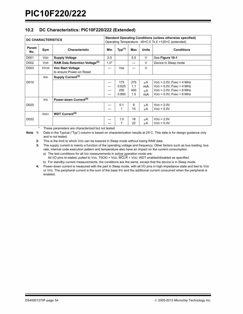
PIC10F220/222
10.2 DC Characteristics: PIC10F220/222 (Extended)DC CHARACTERISTICS Standard Operating Conditions (unless otherwise specified)Operating Temperature -40×C £ TA £ +125×C (extended)
Param No. Sym Characteristic Min Typ(1) Max Units Conditions
D001 VDD Supply Voltage 2.0 5.5 V See Figure 10-1 D002 VDR RAM Data Retention Voltage(2) 1.5* — V Device in Sleep modeD003 VPOR VDD Start Voltage
to ensure Power-on Reset— Vss — V
IDD Supply Current(3)
D010 ————
1750.625250
0.800
2751.14001.5
AmAAmA
VDD = 2.0V, Fosc = 4 MHzVDD = 5.0V, Fosc = 4 MHzVDD = 2.0V, Fosc = 8 MHzVDD = 5.0V, Fosc = 8 MHz
IPD Power-down Current(4)
D020 ——
0.11
915
AA
VDD = 2.0VVDD = 5.0V
IWDT WDT Current(4)
D022 ——
1.07
1822
AA
VDD = 2.0VVDD = 5.0V
* These parameters are characterized but not tested.Note 1: Data in the Typical (“Typ”) column is based on characterization results at 25C. This data is for design guidance only
and is not tested.2: This is the limit to which VDD can be lowered in Sleep mode without losing RAM data.3: The supply current is mainly a function of the operating voltage and frequency. Other factors such as bus loading, bus
rate, internal code execution pattern and temperature also have an impact on the current consumption.a) The test conditions for all IDD measurements in active operation mode are:
All I/O pins tri-stated, pulled to VSS, T0CKI = VDD, MCLR = VDD; WDT enabled/disabled as specified. b) For standby current measurements, the conditions are the same, except that the device is in Sleep mode.
4: Power-down current is measured with the part in Sleep mode, with all I/O pins in high-impedance state and tied to VDD or VSS. The peripheral current is the sum of the base IPD and the additional current consumed when the peripheral is enabled.
DS40001270F-page 54 2005-2013 Microchip Technology Inc.

PIC10F220/222
10.3 DC Characteristics: PIC10F220/222 (Industrial, Extended)DC CHARACTERISTICS
Standard Operating Conditions (unless otherwise specified)Operating temperature -40°C TA +85°C (industrial)
-40°C TA +125°C (extended)Operating voltage VDD range as described in DC specification
ParamNo. Sym Characteristic Min Typ† Max Units Conditions
VIL Input Low VoltageI/O ports:
D030 with TTL buffer Vss — 0.8 V For all 4.5 VDD 5.5VD030A Vss — 0.15 VDD V OtherwiseD031 with Schmitt Trigger
bufferVss — 0.2 VDD V
D032 MCLR, T0CKI Vss — 0.2 VDD VVIH Input High Voltage
I/O ports: —D040 with TTL buffer 2.0 — VDD V 4.5 VDD 5.5VD040A 0.25 VDD + 0.8 — VDD V OtherwiseD041 with Schmitt Trigger
buffer0.8VDD — VDD V For entire VDD range
D042 MCLR, T0CKI 0.8VDD — VDD VD070 IPUR GPIO weak pull-up current 50 250 400 A VDD = 5V, VPIN = VSS
IIL Input Leakage Current(1)
D060 I/O ports — ±0.1 ± 1 A Vss VPIN VDD, Pin at high-imped-ance
D061 GP3/MCLR(2) — ±0.7 ± 5 A Vss VPIN VDD
Output Low VoltageD080 I/O ports — — 0.6 V IOL = 8.5 mA, VDD = 4.5V, -40C to
+85CD080A — — 0.6 V IOL = 7.0 mA, VDD = 4.5V, -40C to
+125COutput High Voltage
D090 I/O ports(2) VDD – 0.7 — — V IOH = -3.0 mA, VDD = 4.5V, -40C to +85C
D090A VDD – 0.7 — — V IOH = -2.5 mA, VDD = 4.5V, -40C to +125C
Capacitive Loading Specs on Output PinsD101 All I/O pins — — 50* pF
† Data in “Typ” column is at 5V, 25C unless otherwise stated. These parameters are for design guidance only and are not tested.
* These parameters are for design guidance only and are not tested.Note 1: Negative current is defined as coming out of the pin.
2: This specification applies when GP3/MCLR is configured as an input with pull-up disabled. The leakage current of the MCLR circuit is higher than the standard I/O logic.
2005-2013 Microchip Technology Inc. DS40001270F-page 55

PIC10F220/222
TABLE 10-1: PULL-UP RESISTOR RANGESVDD (Volts) Temperature (C) Min Typ Max UnitsGP0/GP12.0 -40 73K 105K 186K
25 73K 113K 187K 85 82K 123K 190K 125 86K 132k 190K
5.5 -40 15K 21K 33K 25 15K 22K 34K 85 19K 26k 35K 125 23K 29K 35K
GP32.0 -40 63K 81K 96K
25 77K 93K 116K 85 82K 96k 116K 125 86K 100K 119K
5.5 -40 16K 20k 22K 25 16K 21K 23K 85 24K 25k 28K 125 26K 27K 29K
DS40001270F-page 56 2005-2013 Microchip Technology Inc.

PIC10F220/222
10.4 Timing Parameter Symbology and Load ConditionsThe timing parameter symbols have been created following one of the following formats:FIGURE 10-2: LOAD CONDITIONS
TABLE 10-2: CALIBRATED INTERNAL RC FREQUENCIES – PIC10F220/222
1. TppS2ppS2. TppST
F Frequency T TimeLowercase subscripts (pp) and their meanings:
pp2 to mc MCLR
ck CLKOUT osc Oscillator
cy Cycle time os OSC1
drt Device Reset Timer t0 T0CKI
io I/O port wdt Watchdog Timer
Uppercase letters and their meanings:
SF Fall P Period
H High R Rise
I Invalid (high-impedance) V Valid
L Low Z High-impedance
AC CHARACTERISTICS
Standard Operating Conditions (unless otherwise specified)Operating Temperature -40C TA +85C (industrial),
-40C TA +125C (extended)Operating Voltage VDD range is described inSection 10.1 “DC Characteristics: PIC10F220/222 (Industrial)”.
Param No. Sym Characteristic Freq.
Tolerance Min Typ† Max Units Conditions
F10 FOSC Internal Calibrated INTOSC Frequency(1, 2, 3)
1% 3.96 4.00 4.04 MHz VDD=3.5V @ 25C2% 3.92 4.00 4.08 MHz 2.5V VDD 5.5V
0C TA +85C (industrial)5% 3.80 4.00 4.20 MHz 2.0V VDD 5.5V
-40C TA +85C (industrial)-40C TA +125C (extended)
† Data in the Typical (“Typ”) column is at 5V, 25C unless otherwise stated. These parameters are for design guidance only and are not tested.
Note 1: To ensure these oscillator frequency tolerances, VDD and VSS must be capacitively decoupled as close to the device as possible. 0.1 F and 0.01 F values in parallel are recommended.
2: Under stable VDD conditions.3: Frequency values in this table are doubled when the 8 MHz INTOSC option is selected.
CL
VSS
pin
Legend:CL = 50 pF for all pins
2005-2013 Microchip Technology Inc. DS40001270F-page 57
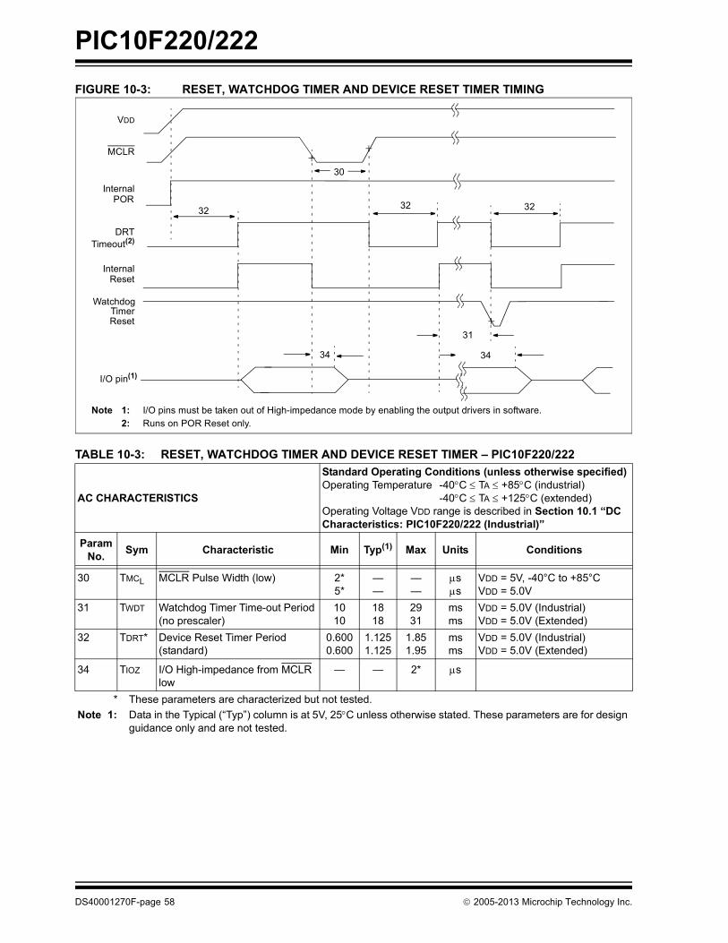
PIC10F220/222
FIGURE 10-3: RESET, WATCHDOG TIMER AND DEVICE RESET TIMER TIMINGTABLE 10-3: RESET, WATCHDOG TIMER AND DEVICE RESET TIMER – PIC10F220/222
AC CHARACTERISTICS
Standard Operating Conditions (unless otherwise specified)Operating Temperature -40C TA +85C (industrial)
-40C TA +125C (extended)Operating Voltage VDD range is described in Section 10.1 “DC Characteristics: PIC10F220/222 (Industrial)”
ParamNo. Sym Characteristic Min Typ(1) Max Units Conditions
30 TMCL MCLR Pulse Width (low) 2*5*
——
——
ss
VDD = 5V, -40°C to +85°CVDD = 5.0V
31 TWDT Watchdog Timer Time-out Period (no prescaler)
1010
1818
2931
msms
VDD = 5.0V (Industrial)VDD = 5.0V (Extended)
32 TDRT* Device Reset Timer Period(standard)
0.6000.600
1.1251.125
1.851.95
msms
VDD = 5.0V (Industrial)VDD = 5.0V (Extended)
34 TIOZ I/O High-impedance from MCLR low
— — 2* s
* These parameters are characterized but not tested.Note 1: Data in the Typical (“Typ”) column is at 5V, 25C unless otherwise stated. These parameters are for design
guidance only and are not tested.
VDD
MCLR
InternalPOR
DRTTimeout(2)
InternalReset
WatchdogTimerReset
32
31
34
I/O pin(1)
32 32
34
30
Note 1: I/O pins must be taken out of High-impedance mode by enabling the output drivers in software.2: Runs on POR Reset only.
DS40001270F-page 58 2005-2013 Microchip Technology Inc.

PIC10F220/222
FIGURE 10-4: TIMER0 CLOCK TIMINGSTABLE 10-4: TIMER0 CLOCK REQUIREMENTS
AC CHARACTERISTICSStandard Operating Conditions (unless otherwise specified)Operating Temperature -40C TA +85C (industrial)
-40C TA +125C (extended)
Param No. Sym Characteristic Min Typ(1) Max Units Conditions
40 Tt0H T0CKI High Pulse Width
No Prescaler 0.5 TCY + 20* — — nsWith Prescaler 10* — — ns
41 Tt0L T0CKI Low Pulse Width
No Prescaler 0.5 TCY + 20* — — nsWith Prescaler 10* — — ns
42 Tt0P T0CKI Period 20 or TCY + 40* N — — ns Whichever is greater.N = Prescale Value(1, 2, 4,..., 256)
* These parameters are characterized but not tested.Note 1: Data in the Typical (“Typ”) column is at 5V, 25°C unless otherwise stated. These parameters are for design
guidance only and are not tested.
T0CKI
40 41
42
2005-2013 Microchip Technology Inc. DS40001270F-page 59

PIC10F220/222
TABLE 10-5: A/D CONVERTER CHARACTERISTICSTABLE 10-6: A/D CONVERSION REQUIREMENTS
Standard Operating Conditions (unless otherwise stated)Operating temperature -40°C TA +125°C
Param No. Sym Characteristic Min Typ† Max Units Conditions
A01 NR Resolution — — 8 bits bitA03 EIL Integral Error — — ±1.5 LSbA04 EDL Differential Error — — -1 < EDL + 1.5 LSbA05 EFS Full-scale Range 2.0* — 5.5* VA06 EOFF Offset Error — — ±1.5 LSbA07 EGN Gain Error — — ±1.5 LSbA10 — Monotonicity — guaranteed(1) — — VSS VAIN VDD
A25 VAIN Analog Input Voltage VSS — VDD VA30 ZAIN Recommended
Impedence of Analog Voltage Source
— — 10 k
A31* IAD A/D Conversion Current(2) — 120 150 A 2.0V— 200 250 A 5.0V
* These parameters are characterized but not tested.† Data in the “Typ” column is at 5.0V, 25°C unless otherwise stated. These parameters are for design
guidance only are not tested.Note 1: The A/D conversion result never decreases with an increase in the input voltage and has no missing
codes.2: This is the additional current consumed by the A/D module when it is enabled; this current adds to base
IDD.
Standard Operating Conditions (unless otherwise stated)Operating temperature -40°C TA +125°C
ParamNo. Sym Characteristic Min Typ† Max Units Conditions
AD131 TCNV Conversion Time(not including Acquisition Time)
— 13 — TCY Set GO/DONE bit to new data in A/D Result register
AD132* TACQ Acquisition Time(1) — 3.55
— ss
VDD = 5VVDD = 2.5V
* These parameters are characterized but not tested.† Data in ‘Typ’ column is at 5.0V, 25°C unless otherwise stated. These parameters are for design guidance
only and are not tested.Note 1: The Section 7.9 “A/D Acquisition Requirements” for information on how to compute minimum
acquisition times based on operating conditions.
DS40001270F-page 60 2005-2013 Microchip Technology Inc.
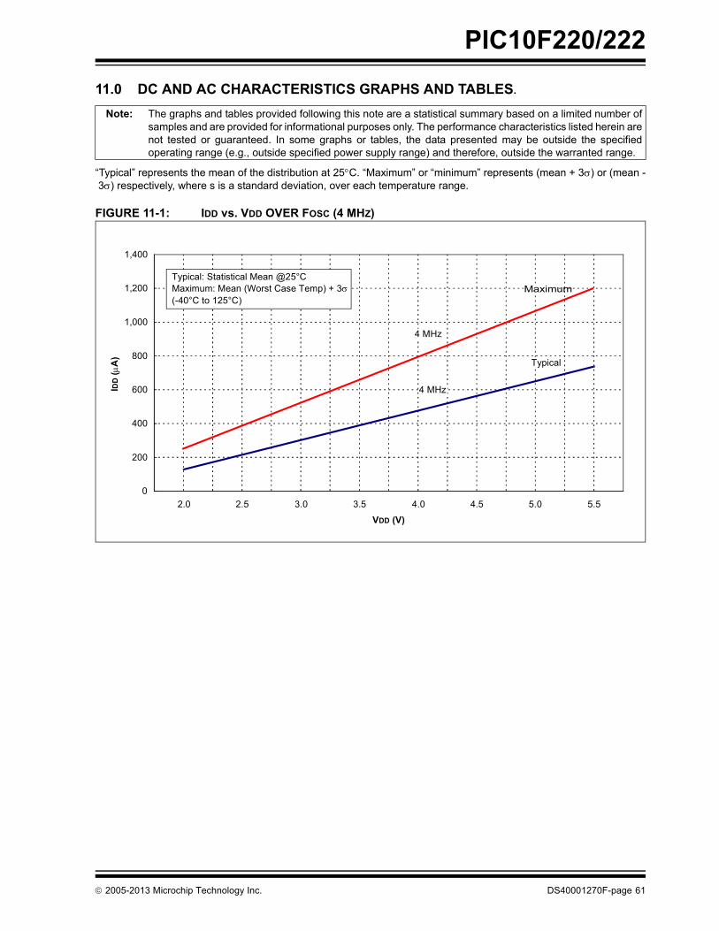
PIC10F220/222
11.0 DC AND AC CHARACTERISTICS GRAPHS AND TABLES.
“Typical” represents the mean of the distribution at 25C. “Maximum” or “minimum” represents (mean + 3) or (mean -3) respectively, where s is a standard deviation, over each temperature range.
FIGURE 11-1: IDD vs. VDD OVER FOSC (4 MHZ)
Note: The graphs and tables provided following this note are a statistical summary based on a limited number ofsamples and are provided for informational purposes only. The performance characteristics listed herein arenot tested or guaranteed. In some graphs or tables, the data presented may be outside the specifiedoperating range (e.g., outside specified power supply range) and therefore, outside the warranted range.
XT Mode
0
200
400
600
800
1,000
1,200
1,400
2.0 2.5 3.0 3.5 4.0 4.5 5.0 5.5
VDD (V)
IDD
(A
)
Typical: Statistical Mean @25°CMaximum: Mean (Worst Case Temp) + 3(-40°C to 125°C)
4 MHz
4 MHz
Maximum
Typical
2005-2013 Microchip Technology Inc. DS40001270F-page 61

PIC10F220/222
FIGURE 11-2: IDD vs. VDD OVER FOSC (8 MHZ)FIGURE 11-3: TYPICAL IPD vs. VDD (SLEEP MODE, ALL PERIPHERALS DISABLED)
Typical(Sleep Mode all Peripherals Disabled)
0.0
200
400
600
800
1,000
1,200
1,400
1,600
1,800
2.0 2.5 3.0 3.5 4.0 4.5 5.0 5.5
VDD (V)
IDD
(A
)
Typical: Statistical Mean @25°CMaximum: Mean (Worst Case Temp) + 3(-40°C to 125°C)
Maximum
Typical
8 MHz
8 MHz
Typical(Sleep Mode all Peripherals Disabled)
0.20
0.30
0.40
0.50
0.60
0.70
0.80
0.90
1.00
1.10
2.0 2.5 3.0 3.5 4.0 4.5 5.0 5.5
VDD (V)
IPD
(A
)
Typical: Statistical Mean @25°C
0.10
0.0
DS40001270F-page 62 2005-2013 Microchip Technology Inc.

PIC10F220/222
FIGURE 11-4: MAXIMUM IPD vs. VDD (SLEEP MODE, ALL PERIPHERALS DISABLED)FIGURE 11-5: TYPICAL WDT IPD vs. VDD
Maximum(Sleep Mode all Peripherals Disabled)
Max. 125°C
Max. 85°C
0.0
2.0
4.0
6.0
8.0
10.0
12.0
14.0
16.0
18.0
2.0 2.5 3.0 3.5 4.0 4.5 5.0 5.5
VDD (V)
IPD
(A
)
Typical: Statistical Mean @25°CMaximum: Mean (Worst Case Temp) + 3(-40°C to 125°C)
0
1
2
3
4
5
6
7
8
9
2.0 2.5 3.0 3.5 4.0 4.5 5.0 5.5
VDD (V)
IPD
(A
)
Typical: Statistical Mean @25°C
2005-2013 Microchip Technology Inc. DS40001270F-page 63

PIC10F220/222
FIGURE 11-6: MAXIMUM WDT IPD vs. VDD OVER TEMPERATUREFIGURE 11-7: WDT TIME-OUT vs. VDD OVER TEMPERATURE (NO PRESCALER)
Maximum
Max. 125°C
Max. 85°C
0.0
5.0
10.0
15.0
20.0
25.0
2.0 2.5 3.0 3.5 4.0 4.5 5.0 5.5VDD (V)
IPD
(A
)
Maximum: Mean (Worst Case Temp) + 3(-40°C to 125°C)
0
5
10
15
20
25
30
35
40
45
50
2.0 2.5 3.0 3.5 4.0 4.5 5.0 5.5VDD (V)
Tim
e (m
s)
Typical: Statistical Mean @25°CMaximum: Mean (Worst Case Temp) + 3(-40°C to 125°C)
Max. 125°C
Max. 85°C
Typical. 25°C
Min. -40°C
DS40001270F-page 64 2005-2013 Microchip Technology Inc.

PIC10F220/222
FIGURE 11-8: VOL vs. IOL OVER TEMPERATURE (VDD = 3.0V)FIGURE 11-9: VOL vs. IOL OVER TEMPERATURE (VDD = 5.0V)
(VDD = 3V, -40×C TO 125×C)
0.0
0.1
0.2
0.3
0.4
0.5
0.6
0.7
0.8
5.0 5.5 6.0 6.5 7.0 7.5 8.0 8.5 9.0 9.5 10.0IOL (mA)
VOL
(V)
Max. 85°C
Max. 125°C
Typical 25°C
Min. -40°C
Typical: Statistical Mean @25°CMaximum: Mean (Worst Case Temp) + 3(-40°C to 125°C)
0.00
0.05
0.10
0.15
0.20
0.25
0.30
0.35
0.40
0.45
5.0 5.5 6.0 6.5 7.0 7.5 8.0 8.5 9.0 9.5 10.0
IOL (mA)
VOL
(V)
Typical: Statistical Mean @25×CMaximum: Meas + 3 (-40×C to 125×C)
Typical: Statistical Mean @25°CMaximum: Mean (Worst Case Temp) + 3(-40°C to 125°C)
Max. 85°C
Typ. 25°C
Min. -40°C
Max. 125°C
2005-2013 Microchip Technology Inc. DS40001270F-page 65

PIC10F220/222
FIGURE 11-10: VOH vs. IOH OVER TEMPERATURE (VDD = 3.0V)FIGURE 11-11: VOH vs. IOH OVER TEMPERATURE (VDD = 5.0V)
0.0
0.5
1.0
1.5
2.0
2.5
3.0
3.5
-4.0-3.5-3.0-2.5-2.0-1.5-1.0-0.50.0IOH (mA)
VOH
(V)
Typ. 25°C
Max. -40°C
Min. 125°C
Typical: Statistical Mean @25°CMaximum: Mean (Worst Case Temp) + 3(-40°C to 125°C)
( , )
3.0
3.5
4.0
4.5
5.0
5.5
-5.0-4.5-4.0-3.5-3.0-2.5-2.0-1.5-1.0-0.50.0IOH (mA)
VOH
(V)
Max. -40°C
Typ. 25°C
Min. 125°C
Typical: Statistical Mean @25°CMaximum: Mean (Worst Case Temp) + 3(-40°C to 125°C)
DS40001270F-page 66 2005-2013 Microchip Technology Inc.

PIC10F220/222
FIGURE 11-12: TTL INPUT THRESHOLD VIN vs. VDDFIGURE 11-13: SCHMITT TRIGGER INPUT THRESHOLD VIN vs. VDD
(TTL Input, -40×C TO 125×C)
0.5
0.7
0.9
1.1
1.3
1.5
1.7
2.0 2.5 3.0 3.5 4.0 4.5 5.0 5.5VDD (V)
VIN
(V) Typ. 25°C
Max. -40°C
Min. 125°C
Typical: Statistical Mean @25°CMaximum: Mean (Worst Case Temp) + 3(-40°C to 125°C)
(ST Input, -40×C TO 125×C)
0.5
1.0
1.5
2.0
2.5
3.0
3.5
4.0
2.0 2.5 3.0 3.5 4.0 4.5 5.0 5.5VDD (V)
VIN
(V)
VIH Max. 125°C
VIH Min. -40°C
VIL Min. 125°C
VIL Max. -40°C
Typical: Statistical Mean @25°CMaximum: Mean (Worst Case Temp) + 3(-40°C to 125°C)
2005-2013 Microchip Technology Inc. DS40001270F-page 67

PIC10F220/222
NOTES:DS40001270F-page 68 2005-2013 Microchip Technology Inc.

PIC10F220/222
12.0 DEVELOPMENT SUPPORTThe PIC® microcontrollers (MCU) and dsPIC® digitalsignal controllers (DSC) are supported with a full rangeof software and hardware development tools:
• Integrated Development Environment- MPLAB® X IDE Software
• Compilers/Assemblers/Linkers- MPLAB XC Compiler - MPASMTM Assembler- MPLINKTM Object Linker/
MPLIBTM Object Librarian- MPLAB Assembler/Linker/Librarian for
Various Device Families• Simulators
- MPLAB X SIM Software Simulator• Emulators
- MPLAB REAL ICE™ In-Circuit Emulator• In-Circuit Debuggers/Programmers
- MPLAB ICD 3- PICkit™ 3
• Device Programmers- MPLAB PM3 Device Programmer
• Low-Cost Demonstration/Development Boards, Evaluation Kits and Starter Kits
• Third-party development tools
12.1 MPLAB X Integrated Development Environment Software
The MPLAB X IDE is a single, unified graphical userinterface for Microchip and third-party software, andhardware development tool that runs on Windows®,Linux and Mac OS® X. Based on the NetBeans IDE,MPLAB X IDE is an entirely new IDE with a host of freesoftware components and plug-ins for high-performance application development and debugging.Moving between tools and upgrading from softwaresimulators to hardware debugging and programmingtools is simple with the seamless user interface.
With complete project management, visual call graphs,a configurable watch window and a feature-rich editorthat includes code completion and context menus,MPLAB X IDE is flexible and friendly enough for newusers. With the ability to support multiple tools onmultiple projects with simultaneous debugging, MPLABX IDE is also suitable for the needs of experiencedusers.
Feature-Rich Editor:
• Color syntax highlighting• Smart code completion makes suggestions and
provides hints as you type• Automatic code formatting based on user-defined
rules• Live parsing
User-Friendly, Customizable Interface:
• Fully customizable interface: toolbars, toolbar buttons, windows, window placement, etc.
• Call graph window
Project-Based Workspaces:
• Multiple projects• Multiple tools• Multiple configurations• Simultaneous debugging sessions
File History and Bug Tracking:
• Local file history feature• Built-in support for Bugzilla issue tracker
2005-2013 Microchip Technology Inc. DS40001270F-page 69

PIC10F220/222
12.2 MPLAB XC CompilersThe MPLAB XC Compilers are complete ANSI Ccompilers for all of Microchip’s 8, 16, and 32-bit MCUand DSC devices. These compilers provide powerfulintegration capabilities, superior code optimization andease of use. MPLAB XC Compilers run on Windows,Linux or MAC OS X.For easy source level debugging, the compilers providedebug information that is optimized to the MPLAB XIDE.
The free MPLAB XC Compiler editions support alldevices and commands, with no time or memoryrestrictions, and offer sufficient code optimization formost applications.
MPLAB XC Compilers include an assembler, linker andutilities. The assembler generates relocatable objectfiles that can then be archived or linked with other relo-catable object files and archives to create an execut-able file. MPLAB XC Compiler uses the assembler toproduce its object file. Notable features of the assem-bler include:
• Support for the entire device instruction set• Support for fixed-point and floating-point data• Command-line interface• Rich directive set• Flexible macro language• MPLAB X IDE compatibility
12.3 MPASM AssemblerThe MPASM Assembler is a full-featured, universalmacro assembler for PIC10/12/16/18 MCUs.
The MPASM Assembler generates relocatable objectfiles for the MPLINK Object Linker, Intel® standard HEXfiles, MAP files to detail memory usage and symbolreference, absolute LST files that contain source linesand generated machine code, and COFF files fordebugging.
The MPASM Assembler features include:
• Integration into MPLAB X IDE projects• User-defined macros to streamline
assembly code• Conditional assembly for multipurpose
source files• Directives that allow complete control over the
assembly process
12.4 MPLINK Object Linker/MPLIB Object Librarian
The MPLINK Object Linker combines relocatableobjects created by the MPASM Assembler. It can linkrelocatable objects from precompiled libraries, usingdirectives from a linker script.
The MPLIB Object Librarian manages the creation andmodification of library files of precompiled code. Whena routine from a library is called from a source file, onlythe modules that contain that routine will be linked inwith the application. This allows large libraries to beused efficiently in many different applications.
The object linker/library features include:
• Efficient linking of single libraries instead of many smaller files
• Enhanced code maintainability by grouping related modules together
• Flexible creation of libraries with easy module listing, replacement, deletion and extraction
12.5 MPLAB Assembler, Linker and Librarian for Various Device Families
MPLAB Assembler produces relocatable machinecode from symbolic assembly language for PIC24,PIC32 and dsPIC DSC devices. MPLAB XC Compileruses the assembler to produce its object file. Theassembler generates relocatable object files that canthen be archived or linked with other relocatable objectfiles and archives to create an executable file. Notablefeatures of the assembler include:
• Support for the entire device instruction set• Support for fixed-point and floating-point data• Command-line interface• Rich directive set• Flexible macro language• MPLAB X IDE compatibility
DS40001270F-page 70 2005-2013 Microchip Technology Inc.

PIC10F220/222
12.6 MPLAB X SIM Software SimulatorThe MPLAB X SIM Software Simulator allows codedevelopment in a PC-hosted environment by simulat-ing the PIC MCUs and dsPIC DSCs on an instructionlevel. On any given instruction, the data areas can beexamined or modified and stimuli can be applied froma comprehensive stimulus controller. Registers can belogged to files for further run-time analysis. The tracebuffer and logic analyzer display extend the power ofthe simulator to record and track program execution,actions on I/O, most peripherals and internal registers.The MPLAB X SIM Software Simulator fully supportssymbolic debugging using the MPLAB XC Compilers,and the MPASM and MPLAB Assemblers. The soft-ware simulator offers the flexibility to develop anddebug code outside of the hardware laboratory envi-ronment, making it an excellent, economical softwaredevelopment tool.
12.7 MPLAB REAL ICE In-Circuit Emulator System
The MPLAB REAL ICE In-Circuit Emulator System isMicrochip’s next generation high-speed emulator forMicrochip Flash DSC and MCU devices. It debugs andprograms all 8, 16 and 32-bit MCU, and DSC deviceswith the easy-to-use, powerful graphical user interface ofthe MPLAB X IDE.
The emulator is connected to the design engineer’sPC using a high-speed USB 2.0 interface and isconnected to the target with either a connectorcompatible with in-circuit debugger systems (RJ-11)or with the new high-speed, noise tolerant, Low-Voltage Differential Signal (LVDS) interconnection(CAT5).
The emulator is field upgradable through future firmwaredownloads in MPLAB X IDE. MPLAB REAL ICE offerssignificant advantages over competitive emulatorsincluding full-speed emulation, run-time variablewatches, trace analysis, complex breakpoints, logicprobes, a ruggedized probe interface and long (up tothree meters) interconnection cables.
12.8 MPLAB ICD 3 In-Circuit Debugger System
The MPLAB ICD 3 In-Circuit Debugger System isMicrochip’s most cost-effective, high-speed hardwaredebugger/programmer for Microchip Flash DSC andMCU devices. It debugs and programs PIC Flashmicrocontrollers and dsPIC DSCs with the powerful,yet easy-to-use graphical user interface of the MPLABIDE.
The MPLAB ICD 3 In-Circuit Debugger probe isconnected to the design engineer’s PC using a high-speed USB 2.0 interface and is connected to the targetwith a connector compatible with the MPLAB ICD 2 orMPLAB REAL ICE systems (RJ-11). MPLAB ICD 3supports all MPLAB ICD 2 headers.
12.9 PICkit 3 In-Circuit Debugger/Programmer
The MPLAB PICkit 3 allows debugging and program-ming of PIC and dsPIC Flash microcontrollers at a mostaffordable price point using the powerful graphical userinterface of the MPLAB IDE. The MPLAB PICkit 3 isconnected to the design engineer’s PC using a full-speed USB interface and can be connected to the tar-get via a Microchip debug (RJ-11) connector (compati-ble with MPLAB ICD 3 and MPLAB REAL ICE). Theconnector uses two device I/O pins and the Reset lineto implement in-circuit debugging and In-Circuit SerialProgramming™ (ICSP™).
12.10 MPLAB PM3 Device ProgrammerThe MPLAB PM3 Device Programmer is a universal,CE compliant device programmer with programmablevoltage verification at VDDMIN and VDDMAX formaximum reliability. It features a large LCD display(128 x 64) for menus and error messages, and a mod-ular, detachable socket assembly to support variouspackage types. The ICSP cable assembly is includedas a standard item. In Stand-Alone mode, the MPLABPM3 Device Programmer can read, verify and programPIC devices without a PC connection. It can also setcode protection in this mode. The MPLAB PM3connects to the host PC via an RS-232 or USB cable.The MPLAB PM3 has high-speed communications andoptimized algorithms for quick programming of largememory devices, and incorporates an MMC card for filestorage and data applications.
2005-2013 Microchip Technology Inc. DS40001270F-page 71

PIC10F220/222
12.11 Demonstration/DevelopmentBoards, Evaluation Kits, and Starter Kits
A wide variety of demonstration, development andevaluation boards for various PIC MCUs and dsPICDSCs allows quick application development on fullyfunctional systems. Most boards include prototypingareas for adding custom circuitry and provide applica-tion firmware and source code for examination andmodification.
The boards support a variety of features, including LEDs,temperature sensors, switches, speakers, RS-232interfaces, LCD displays, potentiometers and additionalEEPROM memory.
The demonstration and development boards can beused in teaching environments, for prototyping customcircuits and for learning about various microcontrollerapplications.
In addition to the PICDEM™ and dsPICDEM™demonstration/development board series of circuits,Microchip has a line of evaluation kits and demonstra-tion software for analog filter design, KEELOQ® securityICs, CAN, IrDA®, PowerSmart battery management,SEEVAL® evaluation system, Sigma-Delta ADC, flowrate sensing, plus many more.
Also available are starter kits that contain everythingneeded to experience the specified device. This usuallyincludes a single application and debug capability, allon one board.
Check the Microchip web page (www.microchip.com)for the complete list of demonstration, developmentand evaluation kits.
12.12 Third-Party Development ToolsMicrochip also offers a great collection of tools fromthird-party vendors. These tools are carefully selectedto offer good value and unique functionality.
• Device Programmers and Gang Programmers from companies, such as SoftLog and CCS
• Software Tools from companies, such as Gimpel and Trace Systems
• Protocol Analyzers from companies, such as Saleae and Total Phase
• Demonstration Boards from companies, such as MikroElektronika, Digilent® and Olimex
• Embedded Ethernet Solutions from companies, such as EZ Web Lynx, WIZnet and IPLogika®
DS40001270F-page 72 2005-2013 Microchip Technology Inc.

PIC10F220/222
13.0 PACKAGING INFORMATION
13.1 Package Marking Information
XXX
8-Lead DFN*
YWWNN
Example
XXXXXNNN
8-Lead PDIP
XXXXXXXX
YYWW
Example
PIC10F220
0520
6-Lead SOT-23*
XXNN
Example
20JR
3eI/P 07Q
BJ06253Q
Legend: XX...X Product-specific informationY Year code (last digit of calendar year)YY Year code (last 2 digits of calendar year)WW Week code (week of January 1 is week ‘01’)NNN Alphanumeric traceability code Pb-free JEDEC® designator for Matte Tin (Sn)* This package is Pb-free. The Pb-free JEDEC designator ( )
can be found on the outer packaging for this package.
Note: In the event the full Microchip part number cannot be marked on one line, it willbe carried over to the next line, thus limiting the number of availablecharacters for customer-specific information.
3e
3e
2005-2013 Microchip Technology Inc. DS40001270F-page 73
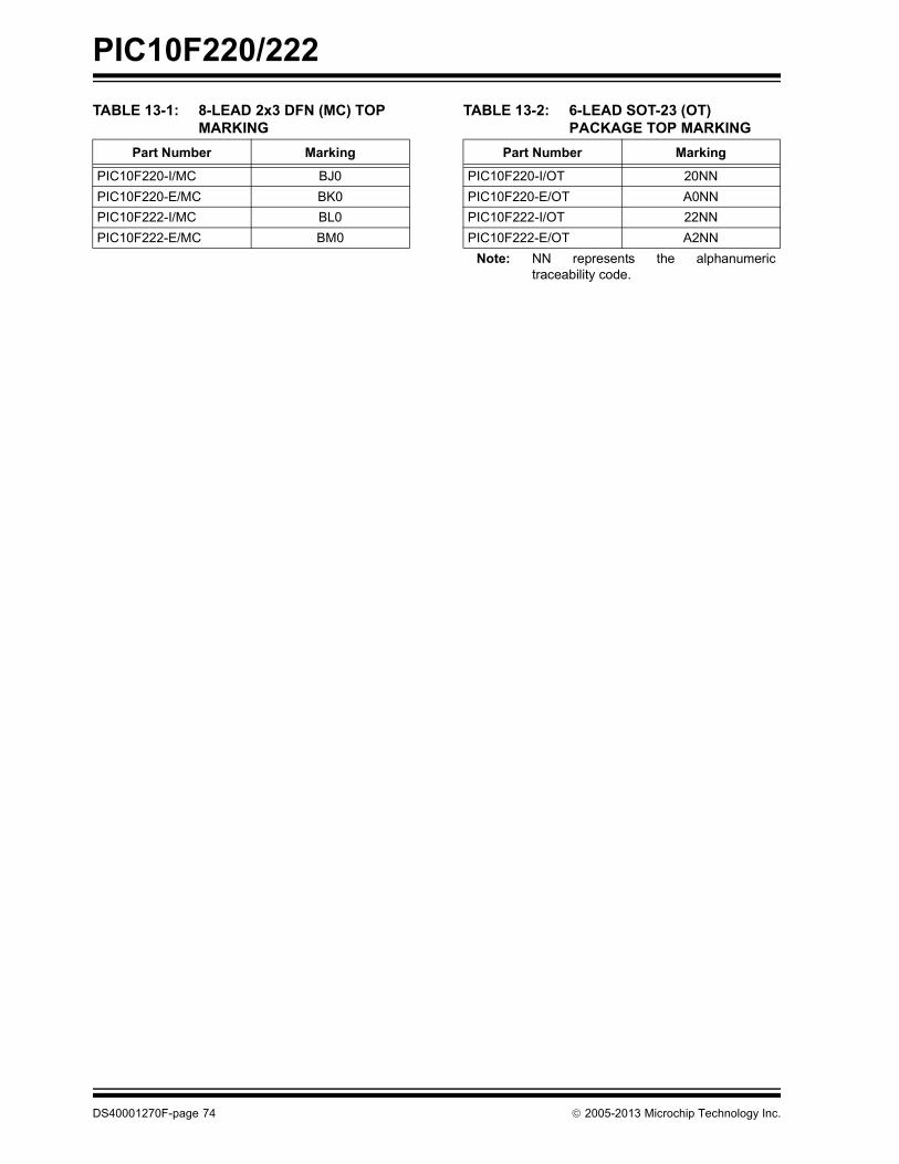
PIC10F220/222
TABLE 13-1: 8-LEAD 2x3 DFN (MC) TOPMARKINGTABLE 13-2: 6-LEAD SOT-23 (OT)
PACKAGE TOP MARKINGPart Number Marking
PIC10F220-I/MC BJ0PIC10F220-E/MC BK0PIC10F222-I/MC BL0PIC10F222-E/MC BM0
Part Number Marking
PIC10F220-I/OT 20NNPIC10F220-E/OT A0NNPIC10F222-I/OT 22NNPIC10F222-E/OT A2NN
Note: NN represents the alphanumerictraceability code.
DS40001270F-page 74 2005-2013 Microchip Technology Inc.

PIC10F220/222
���������� ��������� �������� ������������������
�������� ����� �� �����!�"��!��#�����$!����!�%�� ����#$ �� ����!�%�� ����#$ �� � ������#��&���!������������� �!���� ����� ��������!�#���������������"�'���(��
)�*+ )� �������� ���� ���#��������&��#�,��$�� �-��-�#�$#�#������ �
����� .�#���� #��$��#����/����!�-��� 0����� �� ���#�����������1��/�����������%���#������#�!��#��##�+22---�����������2���/�����
3��# ��44��" "������� ���4���# ��5 56� ��7
5$�8��%�1�� 5 91�#�� � ���(�)�*6$# �!��4��!�1�#�� �� �����)�*6,�����:����# � ���� ; ���(��!�!�1��/���� ���/�� �� ��<� ; �����#��!%% �� ���� ; ���(6,�����=�!#� " ���� ; ������!�!�1��/����=�!#� "� ���� ; ��<�6,�����4���#� � ���� ; ����.#�4���#� 4 ���� ; ��9�.#���# 4� ���( ; ��<�.#������ � �> ; ��>4��!� ���/�� � ���< ; ���94��!�=�!#� 8 ���� ; ��(�
b
E
4N
E1
PIN 1 ID BYLASER MARK
D
1 2 3
e
e1
A
A1
A2 c
LL1
φ
������� ������� ��-��� *�����<)
2005-2013 Microchip Technology Inc. DS40001270F-page 75

PIC10F220/222
Note: For the most current package drawings, please see the Microchip Packaging Specification located at http://www.microchip.com/packaging
DS40001270F-page 76 2005-2013 Microchip Technology Inc.

PIC10F220/222
���������� �� ���!��� ������"��##�� �$��%�� !�
�������� 1�����,� $�����!�&�%��#$������,��0�8$#��$ #�8�����#�!�-�#��#�����#���!������� ?������%����#�*����#�� #����� ����� �� �����!�"��!��#�����$!����!�%�� ����#$ �� ����!�%�� ����#$ �� � ������#��&���!�����@���� �!���� ����� ��������!�#���������������"�'���(��
)�*+�)� �������� ���� ���#��������&��#�,��$�� �-��-�#�$#�#������ �
����� .�#���� #��$��#����/����!�-��� 0����� �� ���#�����������1��/�����������%���#������#�!��#��##�+22---�����������2���/�����
3��# �5*:"������ ���4���# ��5 56� ��7
5$�8��%�1�� 5 <1�#�� � �����)�* ��#����#����1���� � ; ; ������!�!�1��/���� ���/�� �� ���( ���� ���()� ��#����#����1���� �� ���( ; ;��$�!��#���$�!��=�!#� " ���� ���� ���(��!�!�1��/����=�!#� "� ���� ��(� ��<�6,�����4���#� � ���< ��9( ���� ���#����#����1���� 4 ���( ���� ��(�4��!� ���/�� � ���< ���� ���(3����4��!�=�!#� 8� ���� ��9� ����4-��4��!�=�!#� 8 ���� ���< ����6,������-����������? �) ; ; ����
N
E1
NOTE 1
D
1 2 3
A
A1
A2
L
b1b
e
E
eB
c
������� ������� ��-��� *�����<)
2005-2013 Microchip Technology Inc. DS40001270F-page 77

PIC10F220/222
���������� �� ���&��'�����������(�)���*+��"��,�,#-.����$��%�� &��
�������� 1�����,� $�����!�&�%��#$������,��0�8$#��$ #�8�����#�!�-�#����#�����#���!������� 1��/����������,����������&� �!�#���8� ��#���! ��� 1��/����� � �-� ���$��#�!��� ����� ��������!�#���������������"�'���(��
)�*+ )� �������� ���� ���#��������&��#�,��$�� �-��-�#�$#�#������ ��".+ ��%����������� ��0�$ $�����-�#�$#�#������0�%���%��#����$� � �����
����� .�#���� #��$��#����/����!�-��� 0����� �� ���#�����������1��/�����������%���#������#�!��#��##�+22---�����������2���/�����
3��# ��44��" "������� ���4���# ��5 56� ��7
5$�8��%�1�� 5 <1�#�� � ��(��)�*6,�����:����# � ��<� ���� �����#��!%%� �� ���� ���� ���(*�#��#� ���/�� �� ������".6,�����4���#� � �����)�*6,�����=�!#� " �����)�*"&� �!�1�!�4���#� �� ���� ; ��(("&� �!�1�!�=�!#� "� ��(� ; ���(*�#��#�=�!#� 8 ���� ���( ����*�#��#�4���#� 4 ���� ���� ��(�*�#��#�#�"&� �!�1�! A ���� ; ;
D
N
E
NOTE 1
1 2
EXPOSED PAD
NOTE 12 1
D2
K
L
E2
N
eb
A3 A1
A
NOTE 2
BOTTOM VIEWTOP VIEW
������� ������� ��-��� *������*
DS40001270F-page 78 2005-2013 Microchip Technology Inc.

PIC10F220/222
Note: For the most current package drawings, please see the Microchip Packaging Specification located at http://www.microchip.com/packaging
2005-2013 Microchip Technology Inc. DS40001270F-page 79

PIC10F220/222
APPENDIX A: REVISION HISTORY
Revision AOriginal release of document.
Revision B (03/2006)Table 3-1, GP1; Section 4.7, Program Counter; Table 5-2; Figure 8-5; Section 9.1, ANDWF, SLEEP, SUBWF,SWAPF, XORLW.
Revision C (08/2006)Added 8-Lead DFN pinout diagram, updated Table 1-1with DFN package, updated Table 10-3 in Section 10.0,added 8-Lead DFN package marking information tosection 13.0, updated the Product IdentificationSystem section to include DFN package identification.
Added note to package drawings.
Revision D (02/2007)Replaced Dev. Tool Section; Replaced PackageDrawings.
Revision E (06/2007)Updated and added Characterization Data; RevisedOperating Current; Revised Section 8.4 and Note;Revised Section 10.0, Total Power Dissipation, 10.1,10.2, 10.3 DC Characteristics; Revised Tables 10-2,10-3, 10-5, 10-6; Section 11.0; Revised Product IDSystem.
Revision F (10/2013)Revised Packaging Legend.
DS40001270F-page 80 2005-2013 Microchip Technology Inc.

PIC10F220/222
INDEXAA/D
Specifications.............................................................. 60ADC
Internal Sampling Switch (RSS) IMPEDANCE ................ 32Source Impedance...................................................... 32
ALU ....................................................................................... 9Assembler
MPASM Assembler..................................................... 62
BBlock Diagram
On-Chip Reset Circuit ................................................. 36Timer0......................................................................... 25TMR0/WDT Prescaler................................................. 28Watchdog Timer.......................................................... 39
Block DiagramsAnalog Input Model ..................................................... 32
Brown-Out Protection Circuit .............................................. 40
CC Compilers
MPLAB C18 ................................................................ 62MPLAB C30 ................................................................ 62
Carry ..................................................................................... 9Clocking Scheme ................................................................ 11Code Protection ............................................................ 33, 41Configuration Bits................................................................ 33Customer Change Notification Service ............................... 75Customer Notification Service............................................. 75Customer Support ............................................................... 75
DDC and AC Characteristics ................................................. 65Development Support ......................................................... 61Digit Carry ............................................................................. 9
EErrata .................................................................................... 3
FFamily of Devices
PIC10F22X ................................................................... 5FSR..................................................................................... 20
GGPIO ................................................................................... 21
II/O Interfacing ..................................................................... 21I/O Ports .............................................................................. 21I/O Programming Considerations........................................ 23ID Locations .................................................................. 33, 41INDF.................................................................................... 20Indirect Data Addressing..................................................... 20Instruction Cycle ................................................................. 11Instruction Flow/Pipelining .................................................. 11Instruction Set Summary..................................................... 44Internal Sampling Switch (RSS) IMPEDANCE ........................ 32Internet Address.................................................................. 75
LLoading of PC ..................................................................... 19
MMemory Organization ......................................................... 13
Data Memory .............................................................. 14Program Memory (PIC10F220) .................................. 13Program Memory (PIC10F222) .................................. 13
Microchip Internet Web Site................................................ 75MPLAB ASM30 Assembler, Linker, Librarian ..................... 62MPLAB ICD 2 In-Circuit Debugger ..................................... 63MPLAB ICE 2000 High-Performance Universal
In-Circuit Emulator...................................................... 63MPLAB Integrated Development Environment Software.... 61MPLAB PM3 Device Programmer ...................................... 63MPLAB REAL ICE In-Circuit Emulator System .................. 63MPLINK Object Linker/MPLIB Object Librarian .................. 62
OOPTION Register................................................................ 17OSCCAL Register............................................................... 18Oscillator Configurations..................................................... 34Oscillator Types
HS............................................................................... 34LP ............................................................................... 34
PPIC10F220/222 Device Varieties.......................................... 7PICSTART Plus Development Programmer....................... 64POR
Device Reset Timer (DRT) ................................... 33, 38PD............................................................................... 39Power-on Reset (POR)............................................... 33TO............................................................................... 39
Power-down Mode.............................................................. 40Prescaler ............................................................................ 27Program Counter ................................................................ 19
QQ cycles .............................................................................. 11
RReader Response............................................................... 76Read-Modify-Write.............................................................. 23Register File Map
PIC10F220 ................................................................. 14PIC10F222 ................................................................. 14
RegistersSpecial Function ......................................................... 14
Reset .................................................................................. 33Reset on Brown-Out ........................................................... 40
SSleep ............................................................................ 33, 40Software Simulator (MPLAB SIM) ...................................... 62Special Features of the CPU .............................................. 33Special Function Registers ................................................. 14Stack................................................................................... 19STATUS Register ..................................................... 9, 15, 29
TTimer0
Timer0 ........................................................................ 25Timer0 (TMR0) Module .............................................. 25TMR0 with External Clock .......................................... 26
Timing Parameter Symbology and Load Conditions .......... 57TRIS Registers ................................................................... 21
2005-2013 Microchip Technology Inc. DS40001270F-page 81

PIC10F220/222
WWake-up from Sleep ........................................................... 41Watchdog Timer (WDT) ................................................ 33, 38Period.......................................................................... 38Programming Considerations ..................................... 38
WWW Address.................................................................... 75WWW, On-Line Support........................................................ 3
ZZero bit .................................................................................. 9
DS40001270F-page 82 2005-2013 Microchip Technology Inc.

PIC10F220/222
THE MICROCHIP WEB SITEMicrochip provides online support via our WWW site atwww.microchip.com. This web site is used as a meansto make files and information easily available tocustomers. Accessible by using your favorite Internetbrowser, the web site contains the followinginformation:
• Product Support – Data sheets and errata, application notes and sample programs, design resources, user’s guides and hardware support documents, latest software releases and archived software
• General Technical Support – Frequently Asked Questions (FAQ), technical support requests, online discussion groups, Microchip consultant program member listing
• Business of Microchip – Product selector and ordering guides, latest Microchip press releases, listing of seminars and events, listings of Microchip sales offices, distributors and factory representatives
CUSTOMER CHANGE NOTIFICATION SERVICEMicrochip’s customer notification service helps keepcustomers current on Microchip products. Subscriberswill receive e-mail notification whenever there arechanges, updates, revisions or errata related to aspecified product family or development tool of interest.
To register, access the Microchip web site atwww.microchip.com. Under “Support”, click on“Customer Change Notification” and follow theregistration instructions.
CUSTOMER SUPPORTUsers of Microchip products can receive assistancethrough several channels:
• Distributor or Representative• Local Sales Office• Field Application Engineer (FAE)• Technical Support
Customers should contact their distributor,representative or Field Application Engineer (FAE) forsupport. Local sales offices are also available to helpcustomers. A listing of sales offices and locations isincluded in the back of this document.
Technical support is available through the web siteat: http://microchip.com/support
2005-2013 Microchip Technology Inc. DS40001270F-page 83

PIC10F220/222
NOTES:DS40001270F-page 84 2005-2013 Microchip Technology Inc.

2005-2013 Microchip Technology Inc. DS40001270F-page 85
PIC10F220/222
PRODUCT IDENTIFICATION SYSTEMTo order or obtain information, e.g., on pricing or delivery, refer to the factory or the listed sales office.
PART NO. X /XX XXX
PatternPackageTemperatureRange
Device
Device: PIC10F220
PIC10F222PIC10F220T (Tape & Reel)PIC10F222T (Tape & Reel)
Temperature Range:
I = -40C to +85C (Industrial)E = -40C to +125C (Extended)
Package: P = 300 mil PDIP (Pb-free)OT = SOT-23, 6-LD (Pb-free)MC = DFN, 8-LD 2x3 (Pb-free)
Pattern: Special Requirements
Examples:a) PIC10F220-I/P = Industrial temp., PDIP
package (Pb-free)b) PIC10F222T-E/OT = Extended temp., SOT-23
package (Pb-free), Tape and Reelc) PIC10F222-E/MC = Extended temp., DFN
package (Pb-free)

DS40001270F-page 86 2005-2013 Microchip Technology Inc.
AMERICASCorporate Office2355 West Chandler Blvd.Chandler, AZ 85224-6199Tel: 480-792-7200 Fax: 480-792-7277Technical Support: http://www.microchip.com/supportWeb Address: www.microchip.comAtlantaDuluth, GA Tel: 678-957-9614 Fax: 678-957-1455BostonWestborough, MA Tel: 774-760-0087 Fax: 774-760-0088ChicagoItasca, IL Tel: 630-285-0071 Fax: 630-285-0075ClevelandIndependence, OH Tel: 216-447-0464 Fax: 216-447-0643DallasAddison, TX Tel: 972-818-7423 Fax: 972-818-2924DetroitFarmington Hills, MI Tel: 248-538-2250Fax: 248-538-2260IndianapolisNoblesville, IN Tel: 317-773-8323Fax: 317-773-5453Los AngelesMission Viejo, CA Tel: 949-462-9523 Fax: 949-462-9608Santa ClaraSanta Clara, CA Tel: 408-961-6444Fax: 408-961-6445TorontoMississauga, Ontario, CanadaTel: 905-673-0699 Fax: 905-673-6509
ASIA/PACIFICAsia Pacific OfficeSuites 3707-14, 37th FloorTower 6, The GatewayHarbour City, KowloonHong KongTel: 852-2401-1200Fax: 852-2401-3431Australia - SydneyTel: 61-2-9868-6733Fax: 61-2-9868-6755China - BeijingTel: 86-10-8569-7000 Fax: 86-10-8528-2104China - ChengduTel: 86-28-8665-5511Fax: 86-28-8665-7889China - ChongqingTel: 86-23-8980-9588Fax: 86-23-8980-9500China - HangzhouTel: 86-571-2819-3187 Fax: 86-571-2819-3189China - Hong Kong SARTel: 852-2943-5100 Fax: 852-2401-3431China - NanjingTel: 86-25-8473-2460Fax: 86-25-8473-2470China - QingdaoTel: 86-532-8502-7355Fax: 86-532-8502-7205China - ShanghaiTel: 86-21-5407-5533 Fax: 86-21-5407-5066China - ShenyangTel: 86-24-2334-2829Fax: 86-24-2334-2393China - ShenzhenTel: 86-755-8864-2200 Fax: 86-755-8203-1760China - WuhanTel: 86-27-5980-5300Fax: 86-27-5980-5118China - XianTel: 86-29-8833-7252Fax: 86-29-8833-7256China - XiamenTel: 86-592-2388138 Fax: 86-592-2388130China - ZhuhaiTel: 86-756-3210040 Fax: 86-756-3210049
ASIA/PACIFICIndia - BangaloreTel: 91-80-3090-4444 Fax: 91-80-3090-4123India - New DelhiTel: 91-11-4160-8631Fax: 91-11-4160-8632India - PuneTel: 91-20-3019-1500Japan - OsakaTel: 81-6-6152-7160 Fax: 81-6-6152-9310Japan - TokyoTel: 81-3-6880- 3770 Fax: 81-3-6880-3771Korea - DaeguTel: 82-53-744-4301Fax: 82-53-744-4302Korea - SeoulTel: 82-2-554-7200Fax: 82-2-558-5932 or 82-2-558-5934Malaysia - Kuala LumpurTel: 60-3-6201-9857Fax: 60-3-6201-9859Malaysia - PenangTel: 60-4-227-8870Fax: 60-4-227-4068Philippines - ManilaTel: 63-2-634-9065Fax: 63-2-634-9069SingaporeTel: 65-6334-8870Fax: 65-6334-8850Taiwan - Hsin ChuTel: 886-3-5778-366Fax: 886-3-5770-955Taiwan - KaohsiungTel: 886-7-213-7828Fax: 886-7-330-9305Taiwan - TaipeiTel: 886-2-2508-8600 Fax: 886-2-2508-0102Thailand - BangkokTel: 66-2-694-1351Fax: 66-2-694-1350
EUROPEAustria - WelsTel: 43-7242-2244-39Fax: 43-7242-2244-393Denmark - CopenhagenTel: 45-4450-2828 Fax: 45-4485-2829France - ParisTel: 33-1-69-53-63-20 Fax: 33-1-69-30-90-79Germany - MunichTel: 49-89-627-144-0 Fax: 49-89-627-144-44Italy - Milan Tel: 39-0331-742611 Fax: 39-0331-466781Netherlands - DrunenTel: 31-416-690399 Fax: 31-416-690340Spain - MadridTel: 34-91-708-08-90Fax: 34-91-708-08-91UK - WokinghamTel: 44-118-921-5869Fax: 44-118-921-5820
Worldwide Sales and Service
08/20/13