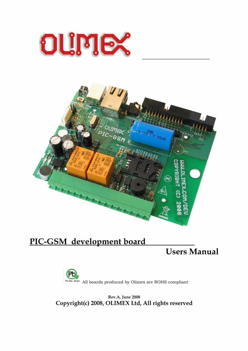
PIC-GSM development board Users Manual · PIC-GSM is excellent board for adding remote monitoring...
26
PIC-GSM development board Users Manual All boards produced by Olimex are ROHS compliant Rev.A, June 2008 Copyright(c) 2008, OLIMEX Ltd, All rights reserved
-
Upload
truongdung -
Category
Documents
-
view
225 -
download
4
Transcript of PIC-GSM development board Users Manual · PIC-GSM is excellent board for adding remote monitoring...
PIC-GSM development board Users Manual
All boards produced by Olimex are ROHS compliant
Rev.A, June 2008Copyright(c) 2008, OLIMEX Ltd, All rights reserved
INTRODUCTION:PIC-GSM is excellent board for adding remote monitoring and control in remote places by GSM cellular network or ethernet or internet network. Do you want to switch on/off your local heating in your mountain house? To monitor the temperature at up to 8 remote points up to 30 meters away from the module? To listen what happens in your house with silent call after you get message for alarm status? Then PIC-GSM is the board for you! It contains PIC18F97J60 microcontroller and 3-band GSM GPRS module 900/1800/1900Mhz inside which covers most used GSM networks around the world. The GSM antenna is build in the board so no need for external expensive GSM antennas. PIC-GSM have two relays 240VAC/10A, two opto-isolated inputs which could be connected to alarm sensors or just buttons for user actions (like call pre-loaded phone numbers), on-board temperature sensor and connector for additional up to 8 addressable remote temperature sensors at up to 30 meter distance from the module. Normal phone hook can be connected to this board and to allow user to speak, listen, taking and placing phone calls as normal stand alone cellular phone. PIC-GSM can be connected to PC with the USB connector it have and it is recognized as modem which could be used to add internet via GPRS to your computer (imagine how useful is this for your mountain house if there is no internet but only cellular network!). If you have internet connection you can monitor the same parameters on the WEB page.
BOARD FEATURES:
• ICSP/ICD connector for programming with PIC-MCP, PIC-MCP-USB, PIC-ICD2, PIC-ICD2-POCKET, PIC-ICD2-TINY;
• USB 2.0 type B connector allow board to be interfaced to PC host;• GSM/GPRS module 900/1800/1900Mhz;• Li-ion backup battery;• PIC18F97J60-I/PT;• Ethernet RJ45 isolated connector.• GSM Audio In and Out;• RS232 connector;• Quartz crystal 20Mhz;• Two relays 10A/250VAC;• Two digital inputs;• Analog input;• Temperature sensor;• 5V voltage regulator;• EXT connector for available GPIO;• Four mounting holes 3,3 mm (0,13");• FR-4, 1.5 mm (0,062"), green soldermask, white silkscreen
component print;• Dimensions 124x90 mm (4880 x 3540 mils);
ELECTROSTATIC WARNING:
The PIC-GSM board is shipped in protective anti-static packaging. The board must not be subject to high electrostatic potentials. General practice for working with static sensitive devices should be applied when working with this board.
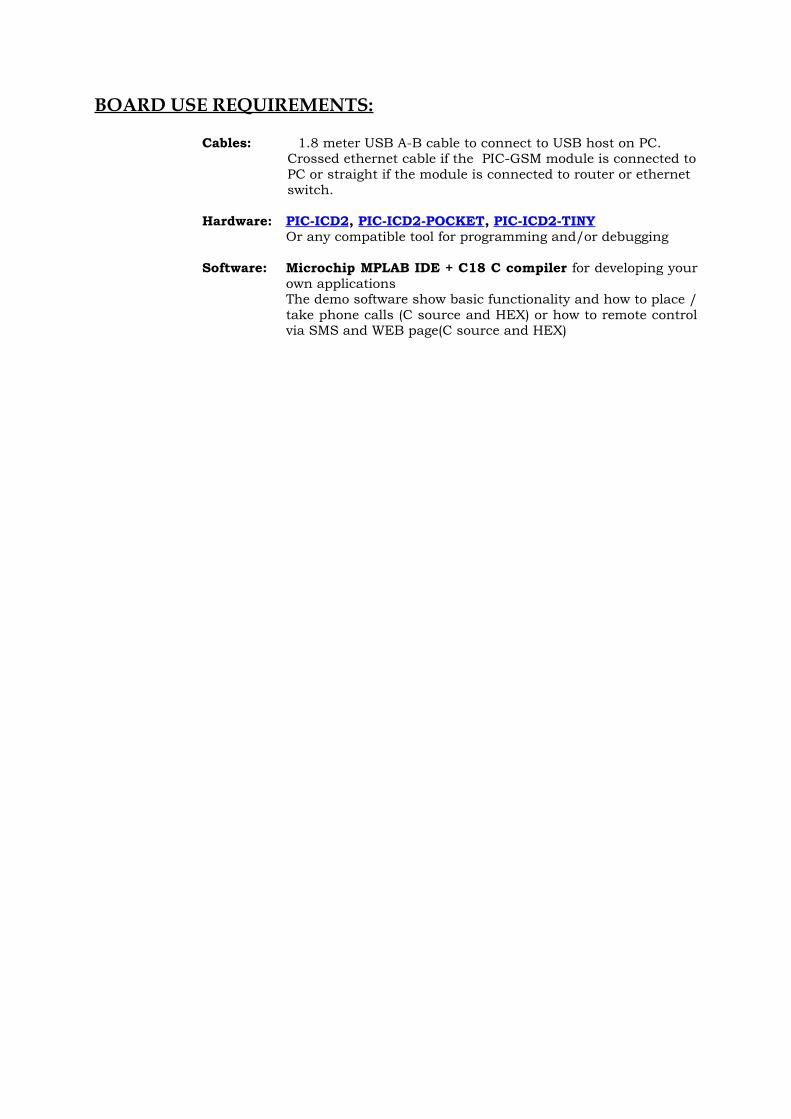
BOARD USE REQUIREMENTS:
Cables: 1.8 meter USB A-B cable to connect to USB host on PC.Crossed ethernet cable if the PIC-GSM module is connected to PC or straight if the module is connected to router or ethernet switch.
Hardware: PIC-ICD2, PIC-ICD2-POCKET, PIC-ICD2-TINYOr any compatible tool for programming and/or debugging
Software: Microchip MPLAB IDE + C18 C compiler for developing your own applicationsThe demo software show basic functionality and how to place / take phone calls (C source and HEX) or how to remote control via SMS and WEB page(C source and HEX)
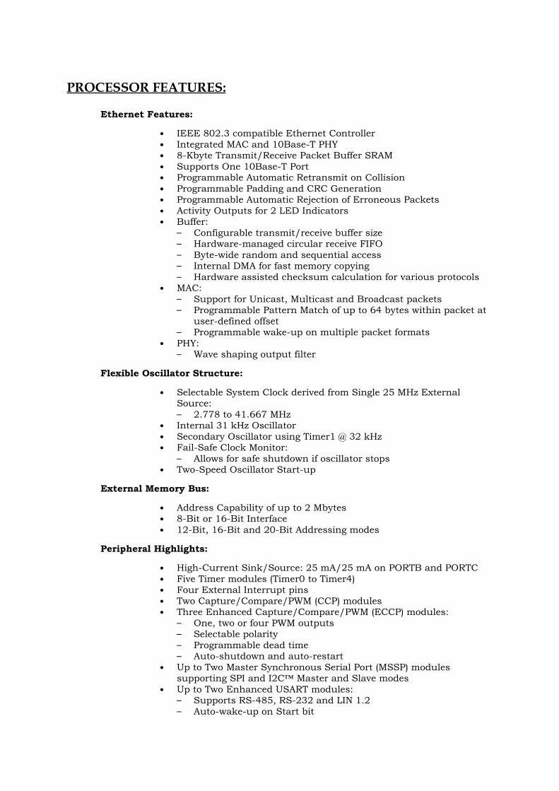
PROCESSOR FEATURES:
Ethernet Features:
• IEEE 802.3 compatible Ethernet Controller• Integrated MAC and 10Base-T PHY• 8-Kbyte Transmit/Receive Packet Buffer SRAM• Supports One 10Base-T Port• Programmable Automatic Retransmit on Collision• Programmable Padding and CRC Generation• Programmable Automatic Rejection of Erroneous Packets• Activity Outputs for 2 LED Indicators• Buffer:– Configurable transmit/receive buffer size– Hardware-managed circular receive FIFO– Byte-wide random and sequential access– Internal DMA for fast memory copying– Hardware assisted checksum calculation for various protocols
• MAC:– Support for Unicast, Multicast and Broadcast packets– Programmable Pattern Match of up to 64 bytes within packet at
user-defined offset– Programmable wake-up on multiple packet formats
• PHY:– Wave shaping output filter
Flexible Oscillator Structure:
• Selectable System Clock derived from Single 25 MHz External Source:– 2.778 to 41.667 MHz
• Internal 31 kHz Oscillator• Secondary Oscillator using Timer1 @ 32 kHz• Fail-Safe Clock Monitor:– Allows for safe shutdown if oscillator stops
• Two-Speed Oscillator Start-up
External Memory Bus:
• Address Capability of up to 2 Mbytes• 8-Bit or 16-Bit Interface• 12-Bit, 16-Bit and 20-Bit Addressing modes
Peripheral Highlights:
• High-Current Sink/Source: 25 mA/25 mA on PORTB and PORTC• Five Timer modules (Timer0 to Timer4)• Four External Interrupt pins• Two Capture/Compare/PWM (CCP) modules• Three Enhanced Capture/Compare/PWM (ECCP) modules:– One, two or four PWM outputs– Selectable polarity– Programmable dead time– Auto-shutdown and auto-restart
• Up to Two Master Synchronous Serial Port (MSSP) modules supporting SPI and I2C™ Master and Slave modes
• Up to Two Enhanced USART modules:– Supports RS-485, RS-232 and LIN 1.2– Auto-wake-up on Start bit
– Auto-Baud Detect (ABD)• 10-Bit, Up to 16-Channel Analog-to-Digital Converter module (A/D):– Auto-acquisition capability– Conversion available during Sleep
• Dual Analog Comparators with Input Multiplexing• Parallel Slave Port (PSP) module (100-pin devices only)
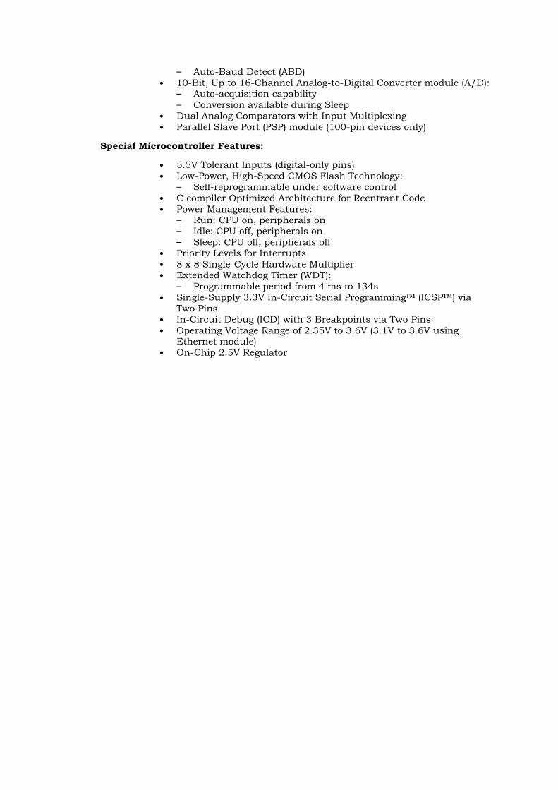
Special Microcontroller Features:
• 5.5V Tolerant Inputs (digital-only pins)• Low-Power, High-Speed CMOS Flash Technology:– Self-reprogrammable under software control
• C compiler Optimized Architecture for Reentrant Code• Power Management Features:– Run: CPU on, peripherals on– Idle: CPU off, peripherals on– Sleep: CPU off, peripherals off
• Priority Levels for Interrupts• 8 x 8 Single-Cycle Hardware Multiplier• Extended Watchdog Timer (WDT):– Programmable period from 4 ms to 134s
• Single-Supply 3.3V In-Circuit Serial Programming™ (ICSP™) via Two Pins
• In-Circuit Debug (ICD) with 3 Breakpoints via Two Pins• Operating Voltage Range of 2.35V to 3.6V (3.1V to 3.6V using
Ethernet module)• On-Chip 2.5V Regulator
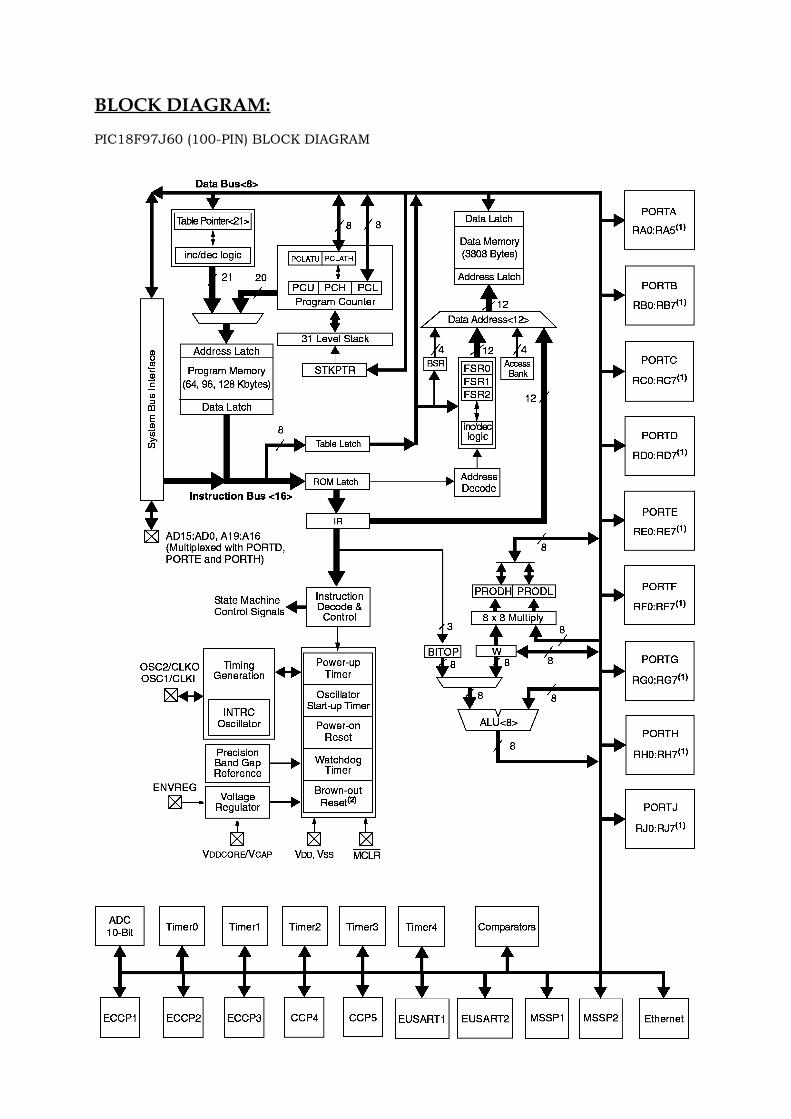
BLOCK DIAGRAM:
PIC18F97J60 (100-PIN) BLOCK DIAGRAM
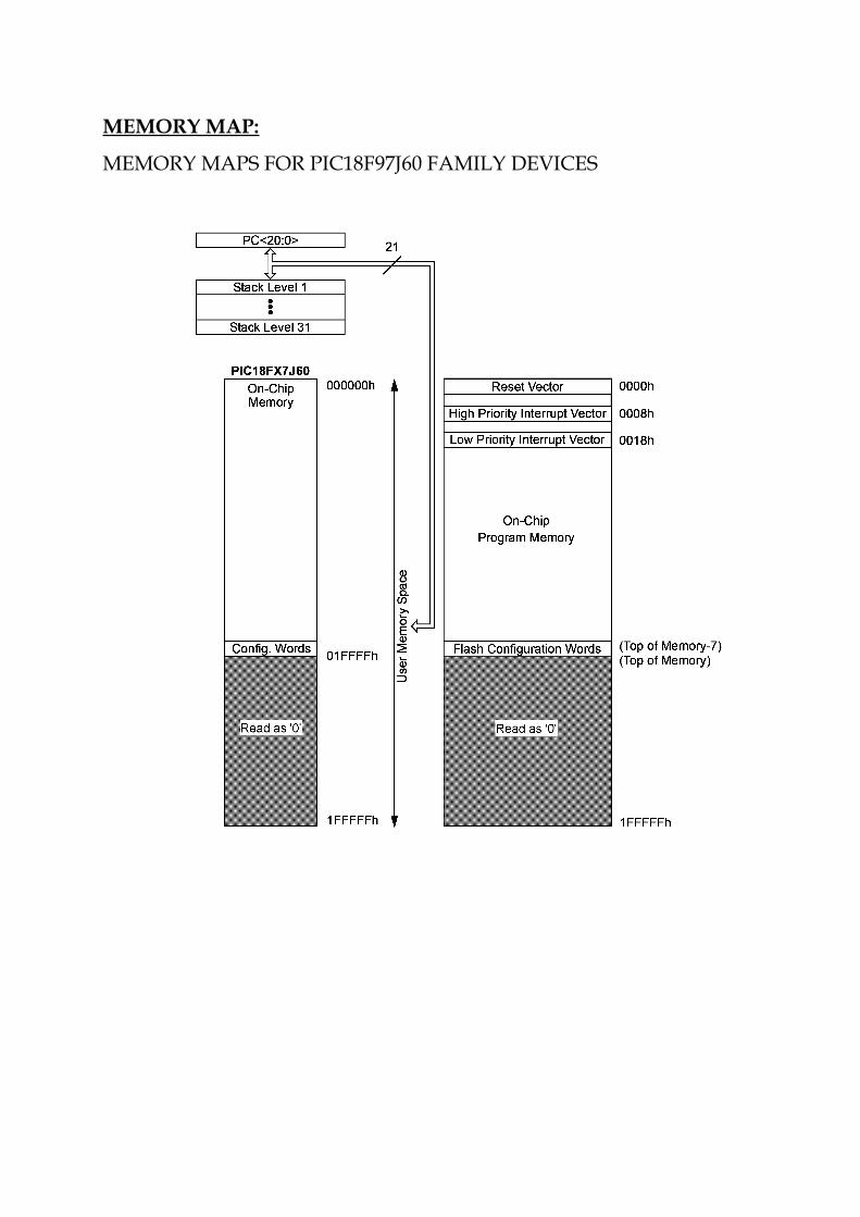
MEMORY MAP:
MEMORY MAPS FOR PIC18F97J60 FAMILY DEVICES
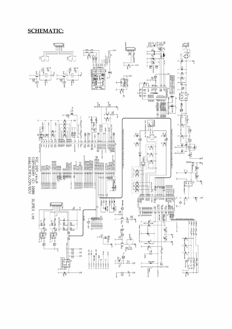
SCHEMATIC:
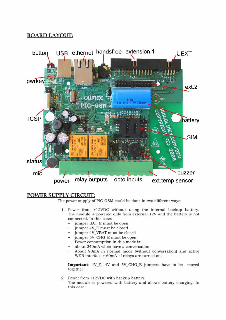
BOARD LAYOUT:
POWER SUPPLY CIRCUIT:The power supply of PIC-GSM could be done in two different ways:
1. Power from +12VDC without using the internal backup battery.The module is powered only from external 12V and the battery is not connected. In this case:− jumper BAT_E must be open− jumper 4V_E must be closed− jumper 4V_VBAT must be closed − jumper 5V_CHG_E must be open.
Power consumption in this mode is:− about 240mA when have a conversation.− About 90mA in normal mode (without conversation) and active
WEB interface + 60mA if relays are turned on.
Important: 4V_E, 4V and 5V_CHG_E jumpers have to be moved together.
2. Power from +12VDC with backup battery.The module is powered with battery and allows battery charging. In this case:
− jumper BAT_E must be closed− jumper 4V_E must be open− jumper 4V_VBAT must be open − jumper 5V_CHG_E must be closed − Power consumption in this mode: depend on the battery charge
may vary between 90mA and 300mA. − If the 12V power supply is missing the battery discharge current
depend from activated microcontroler modules. Max current consumption reach up to 500 mA when all microcontroler moduls are switched on and have a conversation.
RESET CIRCUIT:
PIC-GSM reset circuit is made with RC group and optional STM1001R chip with typical threshold +2.63V. By default STM1001R chip is not assembled
CLOCK CIRCUIT:
Quartz crystal 25MHz is connected to PIC18F97J60.
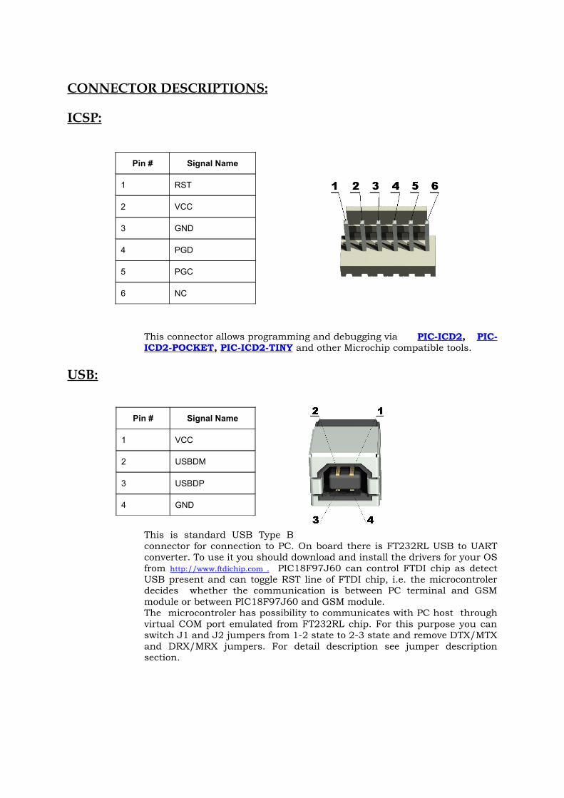
CONNECTOR DESCRIPTIONS:
ICSP:
Pin # Signal Name
1 RST
2 VCC
3 GND
4 PGD
5 PGC
6 NC
This connector allows programming and debugging via PIC-ICD2, PIC-ICD2-POCKET, PIC-ICD2-TINY and other Microchip compatible tools.
USB:
Pin # Signal Name
1 VCC
2 USBDM
3 USBDP
4 GND
This is standard USB Type B connector for connection to PC. On board there is FT232RL USB to UART converter. To use it you should download and install the drivers for your OS from http://www.ftdichip.com . PIC18F97J60 can control FTDI chip as detect USB present and can toggle RST line of FTDI chip, i.e. the microcontroler decides whether the communication is between PC terminal and GSM module or between PIC18F97J60 and GSM module. The microcontroler has possibility to communicates with PC host through virtual COM port emulated from FT232RL chip. For this purpose you can switch J1 and J2 jumpers from 1-2 state to 2-3 state and remove DTX/MTX and DRX/MRX jumpers. For detail description see jumper description section.
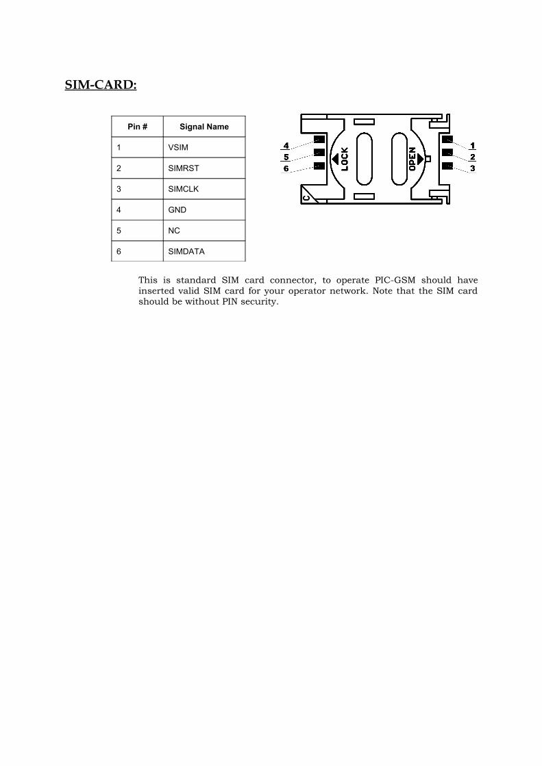
SIM-CARD:
Pin # Signal Name
1 VSIM
2 SIMRST
3 SIMCLK
4 GND
5 NC
6 SIMDATA
This is standard SIM card connector, to operate PIC-GSM should have inserted valid SIM card for your operator network. Note that the SIM card should be without PIN security.
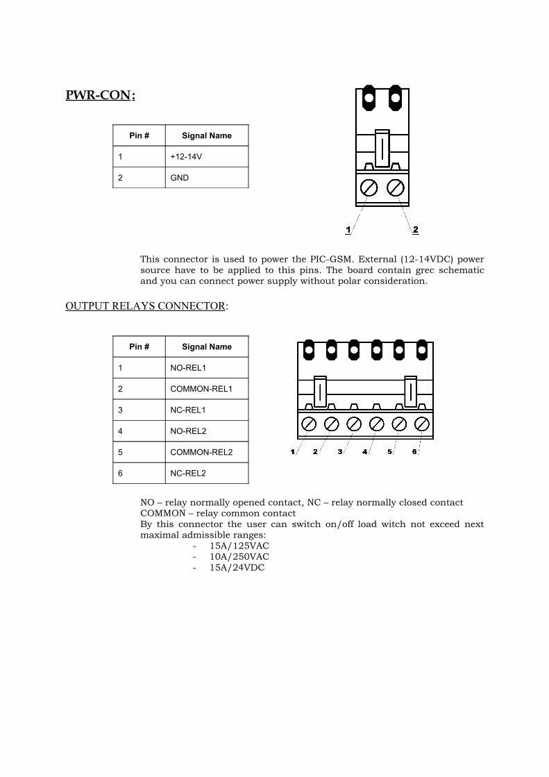
PWR-CON :
Pin # Signal Name
1 +12-14V
2 GND
This connector is used to power the PIC-GSM. External (12-14VDC) power source have to be applied to this pins. The board contain grec schematic and you can connect power supply without polar consideration.
OUTPUT RELAYS CONNECTOR:
Pin # Signal Name
1 NO-REL1
2 COMMON-REL1
3 NC-REL1
4 NO-REL2
5 COMMON-REL2
6 NC-REL2
NO – relay normally opened contact, NC – relay normally closed contactCOMMON – relay common contactBy this connector the user can switch on/off load witch not exceed next maximal admissible ranges:
- 15A/125VAC- 10A/250VAC- 15A/24VDC
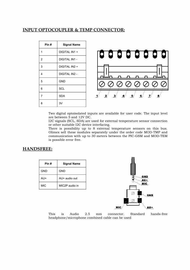
INPUT OPTOCOUPLER & TEMP CONNECTOR:
Pin # Signal Name
1 DIGITAL IN1 +
2 DIGITAL IN1 -
3 DIGITAL IN2 +
4 DIGITAL IN2 -
5 GND
6 SCL
7 SDA
8 3V
Two digital optoisolated inputs are available for user code. The input level are between 5 and 12V DC.I2C signals (SCL, SDA) are used for external temperature sensor connection or other suitable I2C device interfacing.There is possibility up to 8 external temperature sensors on this bus. Olimex sell these modules separately under the order code MOD-TMP and communication with up to 30 meters between the PIC-GSM and MOD-TEM is possible error free.
HANDSFREE:
Pin # Signal Name
GND GND
AU+ AU+ audio out
MIC MIC2P audio in
This is Audio 2.5 mm connector. Standard hands-free headphone/microphone combined cable can be used
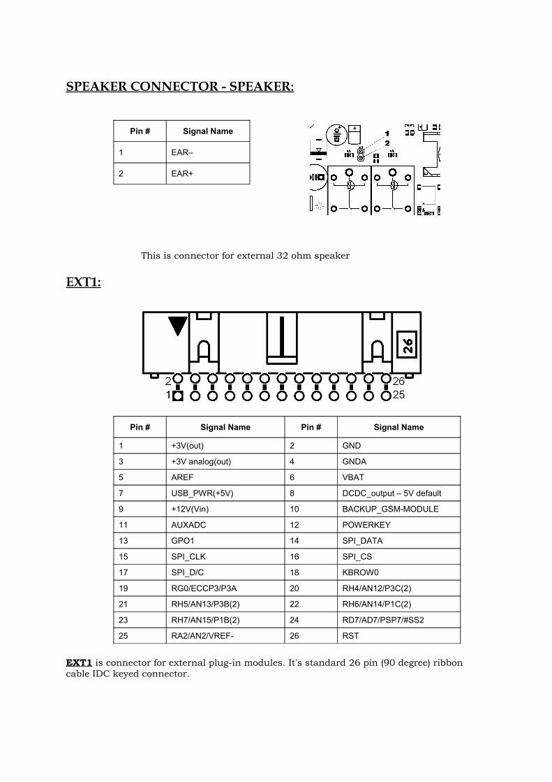
SPEAKER CONNECTOR - SPEAKER:
Pin # Signal Name
1 EAR–
2 EAR+
This is connector for external 32 ohm speaker
EXT1 :
Pin # Signal Name Pin # Signal Name
1 +3V(out) 2 GND
3 +3V analog(out) 4 GNDA
5 AREF 6 VBAT
7 USB_PWR(+5V) 8 DCDC_output – 5V default
9 +12V(Vin) 10 BACKUP_GSM-MODULE
11 AUXADC 12 POWERKEY
13 GPO1 14 SPI_DATA
15 SPI_CLK 16 SPI_CS
17 SPI_D/C 18 KBROW0
19 RG0/ECCP3/P3A 20 RH4/AN12/P3C(2)
21 RH5/AN13/P3B(2) 22 RH6/AN14/P1C(2)
23 RH7/AN15/P1B(2) 24 RD7/AD7/PSP7/#SS2
25 RA2/AN2/VREF- 26 RST
EXT1 is connector for external plug-in modules. It's standard 26 pin (90 degree) ribbon cable IDC keyed connector.
3V: Digital power of PIC18F97J60. This is 3VDC output for external digital modules.GND: Digital ground.
3VA: Analog power supply of PIC18F97J60 microcontroller. This is 3VDC output which can be used for external analog modules.
GNDA: Analog ground of PIC18F97J60 microcontroller. Can be used for external analog circuits.
AREF: Analog reference input of PIC18F97J60 microcontroller. Can be used for external analogue circuits.
VBAT: Dedicated to connect main Li-ion battery. The power supply of GSM module has to be a single voltage source of VBAT= 3.4V...4.5V. Li-ion battery with 650mA capacity is used in PIC-GSM.
USB-PWR. +5V output direct connected to +5V of the USB connector.
DCDC-OUTPUT. 5V or 4V output (up to 2A) from DCDC converter depending on jumper configuration. For details see jumper description section.
+12V(Vin). Input or output terminal for power supply. If the power source is connected to the module this terminal can use as +12V output . Otherwise this terminal can use for power source input.
Backup: RTC backup power supply for the GSM module real time clock and RAM, when the battery is discharged. If the battery attached to this signal is chargeable and the voltage level is low the module will charge the battery. Vnom = 1.8V, Inom= 20uA
AUXADC: This is general purpose analog to digital converter build-in the GSM module. The input voltage value should be in range 0V to 2.4V. This pin value can be read with AT command.
POWERKEY: This is GSM module power on/off key. When the module is ON if you press and hold for more than 3 seconds the module go in power down state. If the module if in power down mode and you press and hold this key for more than 1 second the module will go in ON mode.
GPO1: This is GPO of GSM module and can be configured by AT command for outputting high or low level voltage. All of the GPOs are initialy in low state without any setting from AT command.
SPI_DATA,SPI_CLK,SPI_CS,SPI_D/C: This is GSM module SPI port reserved for future use.
KBROW0: This is external keyboard input pin of GSM module.
RG0/ECCP3/P3A, RG0/ECCP3/P3A, RH5/AN13/P3B(2), RH6/AN14/P1C(2), RH7/AN15/P1B(2), RD7/AD7/PSP7/#SS2, RA2/AN2/VREF- These are PIC18F97J60 port pins.
RST: PIC18F97J60 Reset pin.
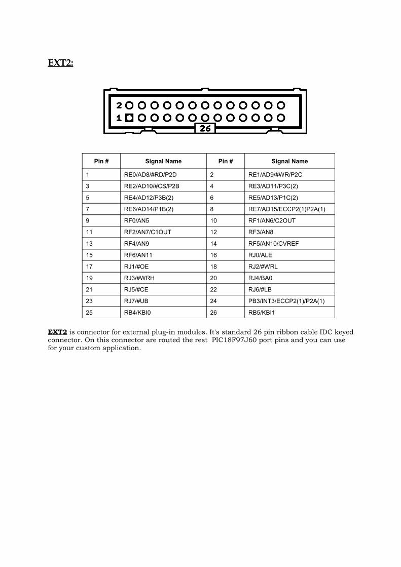
EXT2:
Pin # Signal Name Pin # Signal Name
1 RE0/AD8/#RD/P2D 2 RE1/AD9/#WR/P2C
3 RE2/AD10/#CS/P2B 4 RE3/AD11/P3C(2)
5 RE4/AD12/P3B(2) 6 RE5/AD13/P1C(2)
7 RE6/AD14/P1B(2) 8 RE7/AD15/ECCP2(1)P2A(1)
9 RF0/AN5 10 RF1/AN6/C2OUT
11 RF2/AN7/C1OUT 12 RF3/AN8
13 RF4/AN9 14 RF5/AN10/CVREF
15 RF6/AN11 16 RJ0/ALE
17 RJ1/#OE 18 RJ2/#WRL
19 RJ3/#WRH 20 RJ4/BA0
21 RJ5/#CE 22 RJ6/#LB
23 RJ7/#UB 24 PB3/INT3/ECCP2(1)/P2A(1)
25 RB4/KBI0 26 RB5/KBI1
EXT2 is connector for external plug-in modules. It's standard 26 pin ribbon cable IDC keyed connector. On this connector are routed the rest PIC18F97J60 port pins and you can use for your custom application.
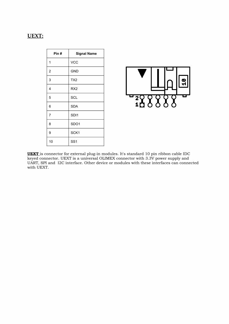
UEXT:
Pin # Signal Name
1 VCC
2 GND
3 TX2
4 RX2
5 SCL
6 SDA
7 SDI1
8 SDO1
9 SCK1
10 SS1
UEXT is connector for external plug-in modules. It's standard 10 pin ribbon cable IDC keyed connector. UEXT is a universal OLIMEX connector with 3.3V power supply and UART, SPI and I2C interface. Other device or modules with these interfaces can connected with UEXT.
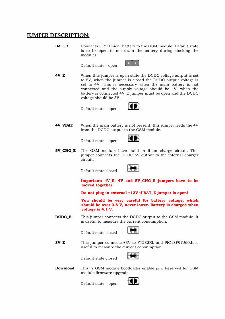
JUMPER DESCRIPTION:
BAT_E Connects 3.7V Li-ion battery to the GSM module. Default state is to be open to not drain the battery during stocking the modules.
Default state - open
4V_E When this jumper is open state the DCDC voltage output is set to 5V, when the jumper is closed the DCDC output voltage is set to 4V. This is necessary when the main battery is not connected and the supply voltage should be 4V, when the battery is connected 4V_E jumper must be open and the DCDC voltage should be 5V.
Default state – open.
4V_VBAT When the main battery is not present, this jumper feeds the 4V from the DCDC output to the GSM module.
Default state – open.
5V_CHG_E The GSM module have build in li-ion charge circuit. This jumper connects the DCDC 5V output to the internal charger circuit.
Default state closed
Important: 4V_E, 4V and 5V_CHG_E jumpers have to be moved together.
Do not plug in external +12V if BAT_E jumper is open!
You should be very careful for battery voltage, which should be over 3.8 V, never lower. Battery is charged when voltage is 4.1 V.
DCDC_E This jumper connects the DCDC output to the GSM module. It is useful to measure the current consumption.
Default state closed
3V_E This jumper connects +3V to FT232RL and PIC18F97J60.It is useful to measure the current consumption.
Default state closed
Download This is GSM module bootloader enable pin. Reserved for GSM module firmware upgrade.
Default state – open.
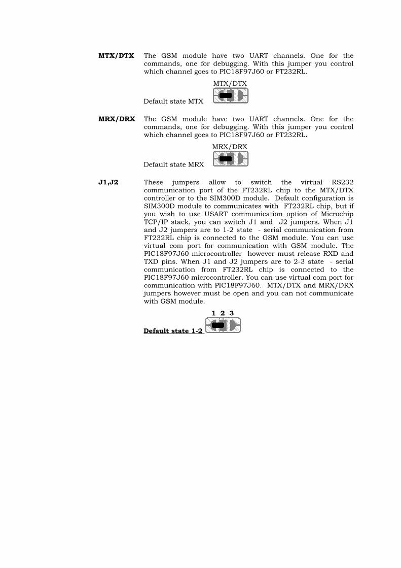
MTX/DTX The GSM module have two UART channels. One for the commands, one for debugging. With this jumper you control which channel goes to PIC18F97J60 or FT232RL.
MTX/DTX
Default state MTX
MRX/DRX The GSM module have two UART channels. One for the commands, one for debugging. With this jumper you control which channel goes to PIC18F97J60 or FT232RL.
MRX/DRX
Default state MRX
J1,J2 These jumpers allow to switch the virtual RS232 communication port of the FT232RL chip to the MTX/DTX controller or to the SIM300D module. Default configuration is SIM300D module to communicates with FT232RL chip, but if you wish to use USART communication option of Microchip TCP/IP stack, you can switch J1 and J2 jumpers. When J1 and J2 jumpers are to 1-2 state - serial communication from FT232RL chip is connected to the GSM module. You can use virtual com port for communication with GSM module. The PIC18F97J60 microcontroller however must release RXD and TXD pins. When J1 and J2 jumpers are to 2-3 state - serial communication from FT232RL chip is connected to the PIC18F97J60 microcontroller. You can use virtual com port for communication with PIC18F97J60. MTX/DTX and MRX/DRX jumpers however must be open and you can not communicate with GSM module.
1 2 3
Default state 1-2
INPUT/OUTPUT:
LAN: RJ45 isolated ethernet connector. You can connect to PC host(with crossed cable), router or ethernet switch. The default IP address is: 192.168.0.105. The main page properties are described in software section. Button B1: user button connected to PIC18F97J60 pin.6 RB1 (INT1);
PWRKEY button – This is GSM module power on/off key. When the module is ON if you press and hold for more than 3 seconds the module go in power down state. If the module if in power down mode and you press and hold this key for more than 1 second the module will go in ON mode.
MIC – on-board microphone (voice), with AT command you can switch the voice audio input to be taken from this microphone of from the handsfree audio connector.
SPEAKER – voice output for external 32 ohm speaker, with AT command you can switch the voice audio output to be directed to this speaker or to the handsfree audio connector.
HANDSFREE – audio 2.5 mm jack microphone input and speaker output.
BUZ – audio buzzer , can be used as RING signalization. Status green LED with name LED connected to PIC18F97J60 pin.11 RG5.
Status red LED with name STAT – indicates the state of GSM module.STAT is off state – GSM module is not running64ms On/ 800ms Off – GSM module does not find the network64ms On/ 3000ms Off – GSM module is connected to the network64ms On/ 300ms Off - GPRS communication
Optocouple 1 – OPT1 (H11A817SMD) - 5V-12V optoisolated input with LED2 indication and open collector output connect to PIC18F97J60 pin.51 (CCP4/P3D). Positive voltage of '+' terminal and negative voltage or GND of '-' terminal of OPT_TEMP connector, reflect with log. 0 of PIC18F97J60 input.
Optocouple 2 – OPT2 (H11A817SMD) - 5V-12V optoisolated input with LED3 indication and open collector output connect to PIC18F97J60 pin.14 (PG4/CCP5/P1D).Positive voltage of '+' terminal and negative voltage or GND of '-' terminal of OPT_TEMP connector, reflect with log. 0 of PIC18F97J60 input.
Relay1 – REL1 240VAC/10A (RAS1215) with default tied Normal Close (NC) and COM terminals and disconnected Normal Open and COM terminals. LED_R1 (Red) indicated when turn on REL1. The relay is turned on with log 1 of PG7 port.
Relay2 – REL2 240VAC/10A (RAS1215) with default tied Normal Close (NC) and COM terminals and disconnected Normal Open and COM terminals. LED_R2 (Red) indicated when turn on REL2. The relay is turned on with log 1 of PG6 port.
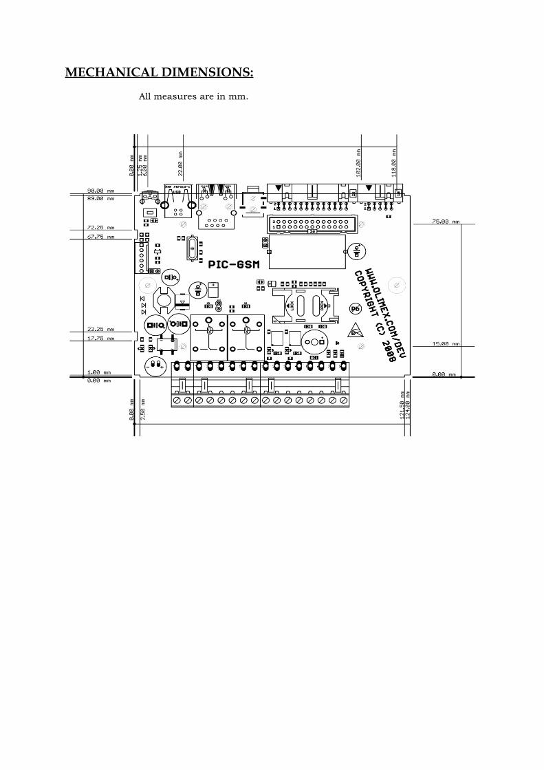
MECHANICAL DIMENSIONS:
All measures are in mm.
AVAILABLE DEMO SOFTWARE:
2. Software notes
Software, that PIC-GSM board is shipped with, includes Microchip TCP/IP stack is combined with simple functionality for making calls and sending SMS with SIM300D GSM/GPRS module. This note explains features of PIC-GSM board. For more information on the Microchip TCP/IP Stack, please refer to application note AN833 available at http://www.microchip.com.
SMS sending functionality is strongly dependent of serial communication between PIC18F67J60 MCU and SIM300D module. Consequently board software functions are very sensitive to any messages send from SIM300D module. For example, when SIM300D module goes to specific states(POWER DOWN, Call Ready etc), it sends indicating messages via serial line, which can affect communication with PIC18F97J60 and cause wrong behavior of software.
Specific features:• First time you insert power to board USB should not be connected to board due to
initialization procedures between PIC and GSM module.• UART baud rate, which ensures best performance is 115200 bps. Other specific
features, which software rely on are:• Disable echo(command used is ATE0)• Set SMS text format (command used is AT+CMGF=1)
• After board power-up software continuously sends “AT” command expecting “OK” string, ensuring proper communication with GSM module.
• Software allows to dial GSM and make GSM call, getting GSM number or SMS text from web page form. GSM number length is 16 digits
• Software allows sending SMS getting GSM number and SMS text from web page forms. GSM number must be typed with country code without “+” sign. GSM number length is 16 digits and SMS message length 32 digits.
• Status page item “Open Call” displays information about call processing .”0” indicates that no call is in process. “1” indicates that GSM call is in process. (After GSM number is dialed, “Open Call” value is set to “1”, if other side close call after a while “Open Call” value returns back to “0”. If other side accept call, “Open Call” value remains “1”, for the time of call is in process. When call is closed “Open Call” value is set back to “0”)
• PIC-GSM Board has 2 audio channels – one connected to MIC, and auxiliary connected to HANDSFREE. You can switch to next audio channel by pressing button B1.
• Pressing button toggle the on board buzzer unless the GSM module is not in open call mode.
• When you plug USB cable to the board, the FTDI chip on the board emulates virtual COM port and you can connect to SIM300D module with HyperTerminal. First however have to install FTDI drivers available on the http://www.ftdichip.com/
• Temperature, displayed on web page is read from SIM300D module with AT command (AT+CMTE?). Any problem with correct displaying temperature, is related with correct handling of used AT command output or GSM module response. This measurement should not be treated as reliable .
• Another useful feature is ability of getting temperatures from up to 8 external temperature sensors TCN75A connected via I2C interface. In "Temperature sensors presence" each item stands for presence of sensor with given hardware address 000 for Temp sensor 1, 001 for temp sensor 2, ... and 111 for temp sensor 8. "Temperature measured by sensors" section contains temperature in C° measured by sensor(s) available.
• Items: Relay 1, Relay 2 and LED buttons from “Status” section display voltage applied to corresponding input/output 1- high voltage; 0 – low voltage.
Log “1” of Relay1 (PG7) and Relay2 (PG6) outputs means that the Relay is turned on, while log “0” mean that the Relay is turned off. Log “1” to the LED output (PG5) means that LED is turned off, while log “0” mean that the LED is turned on. Logical “1” on Opto input 1(RG3) and Opto input 2 (RG4) means that high voltage is applied to the input
• Status page item “seconds” displays seconds elapsed from program start, measured by RTC.
• Status page item “Uin” displays input voltage in Volts, measured on RA5(AN4) pin . • “Test board area” section is not intended for user examination and shouldn't be used
by customer.Advices to customer for further use:
• User should be familiar with basic AT commands(make call, send SMS, read SMS etc).
• SIM card, you put should be with disabled PIN code use. So before use, put SIM card in normal GSM and disable PIN code use.

ORDER CODE:How to order? You can order to us directly or by any of our distributors. Check our web www.olimex.com/dev for more info.
All boards produced by Olimex are ROHS compliant
Revision history:
REV.A - create April 2008
Disclaimer: © 2008 Olimex Ltd. All rights reserved. Olimex®, logo and combinations thereof, are registered trademarks of Olimex Ltd. Other terms and product names may be trademarks of others.The information in this document is provided in connection with Olimex products. No license, express or implied or otherwise, to any intellectual property right is granted by this document or in connection with the sale of Olimex products. Neither the whole nor any part of the information contained in or the product described in this document may be adapted or reproduced in any material from except with the prior written permission of the copyright holder.The product described in this document is subject to continuous development and improvements. All particulars of the product and its use contained in this document are given by OLIMEX in good faith. However all warranties implied or expressed including but not limited to implied warranties of merchantability or fitness for purpose are excluded.This document is intended only to assist the reader in the use of the product. OLIMEX Ltd. shall not be liable for any loss or damage arising from the use of any information in this document or any error or omission in such information or any incorrect use of the product.