PIC DevBugger Manual - Ningapi.ning.com/.../DevBuggerManual_Summer_2010.pdf · · 2017-05-26PIC...
30
AER201 – Engineering Design PIC DevBugger Manual
Transcript of PIC DevBugger Manual - Ningapi.ning.com/.../DevBuggerManual_Summer_2010.pdf · · 2017-05-26PIC...

AER201 – Engineering Design
PIC DevBugger Manual
PIC DevBugger Manual Table of Contents Table of Contents ................................................................................................................ 2 1. Introduction ................................................................................................................. 3
1.1 Overview .............................................................................................................. 3 1.2 Features ................................................................................................................ 4 1.3 Included in the Box .............................................................................................. 4
2. Operation..................................................................................................................... 5 2.1 Operational Modes ............................................................................................... 5 2.2 Connecting to the PC for Programming ............................................................... 5 2.3 Customizing Board Operation .............................................................................. 6 2.4 Interfacing with External Circuits ........................................................................ 6
3. Board Modules ............................................................................................................ 7 3.1 Power Supply ....................................................................................................... 7 3.2 On-board USB Programmer ................................................................................. 7 3.3 Debugging Module ............................................................................................... 8 3.4 HD44780 Based LCD .......................................................................................... 9 3.5 4x4 KEYPAD ....................................................................................................... 9 3.6 RS-232 DB-9 Communication ........................................................................... 10 3.7 A2D Reference ................................................................................................... 10 3.8 Real Time Clock ................................................................................................. 10
3.8.1 Using the Real Time Clock ......................................................................... 10 3.9 Main I/O BUS .................................................................................................... 13 3.10 I2C BUS .......................................................................................................... 13 3.11 Main PIC Device ............................................................................................ 14
4. Programming Software ............................................................................................. 15 4.1 Overview ............................................................................................................ 15 4.2 Quick Start .......................................................................................................... 15 4.3 Operations .......................................................................................................... 16 4.4 Additional Features of PICusb ........................................................................... 16 4.5 Sample Code ...................................................................................................... 18
5. Advanced Programming Topics ............................................................................... 21 5.1 Overview ............................................................................................................ 21 5.2 Coding Firmware Modifications ........................................................................ 21
5.2.1 Modifying Run-Mode ................................................................................. 21 5.2.2 Re-Imaging the PIC18F2550 ...................................................................... 23 5.2.3 User Code Considerations........................................................................... 23
5.3 Restoring to Original State ................................................................................. 24 6. I2C PIC to PIC Communication ................................................................................ 26
6.1 I2C Overview ...................................................................................................... 26 6.2 Using the I2C ...................................................................................................... 26
6.2.1 PIC-RTC Communication .......................................................................... 27 6.2.2 PIC-to-PIC Communication for Parallel Processing .................................. 27 6.2.3 PIC-to-PIC Extending I/O Set Programming ............................................. 27 6.2.4 PIC16-PIC18 Communication for PIC16 Register Watching .................... 28 6.2.5 PIC- I2C Bus Communication ..................................................................... 29
2 Version 3.0
PIC DevBugger Manual
6.3 Important Note About i2c_common.asm and Its Macros .................................. 30
1. Introduction
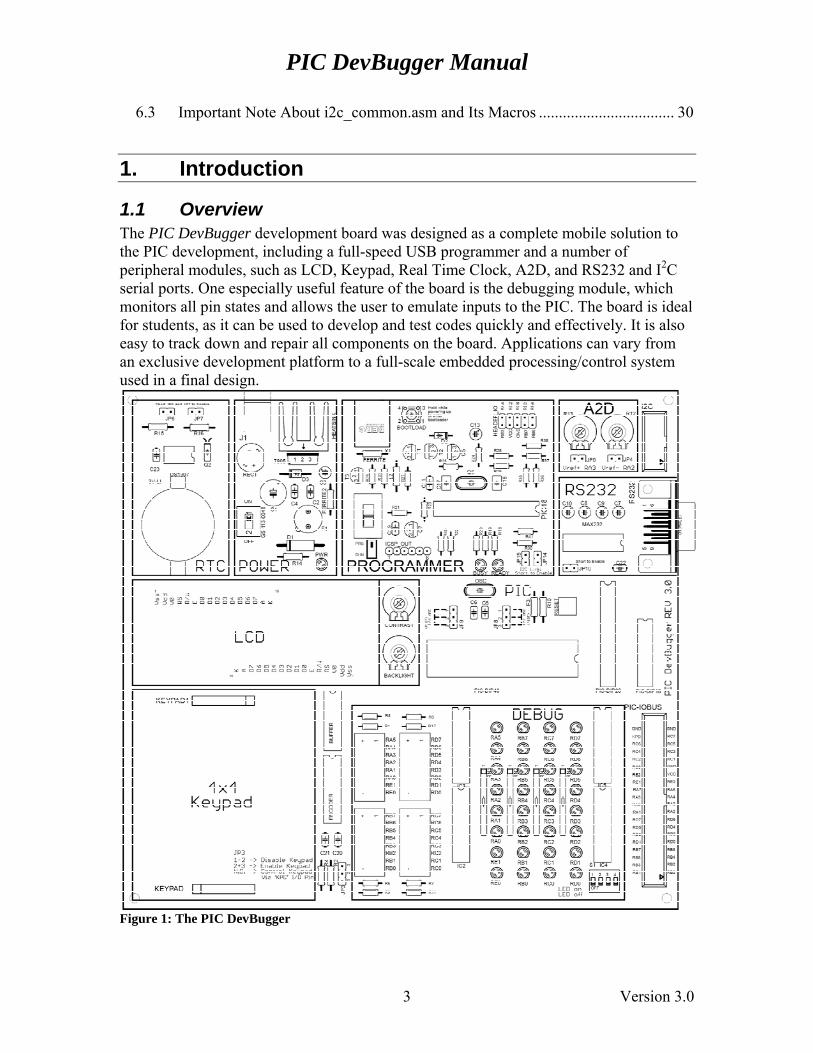
1.1 Overview The PIC DevBugger development board was designed as a complete mobile solution to the PIC development, including a full-speed USB programmer and a number of peripheral modules, such as LCD, Keypad, Real Time Clock, A2D, and RS232 and I2C serial ports. One especially useful feature of the board is the debugging module, which monitors all pin states and allows the user to emulate inputs to the PIC. The board is ideal for students, as it can be used to develop and test codes quickly and effectively. It is also easy to track down and repair all components on the board. Applications can vary from an exclusive development platform to a full-scale embedded processing/control system used in a final design.
Figure 1: The PIC DevBugger
3 Version 3.0

PIC DevBugger Manual 1.2 Features
Open, modular, and simple design for learning purposes Supports a wide range of implementations, from simple MCU operation to
parallel processing, memory extension, serial communication, etc. Supports 18-, 28-, and 40-pin packages for PIC16 and 18 families In-circuit USB High Voltage Programmer (compatible with MPLAB® IDE) Dual USB-adaptor power supply (ranging from 7.5VDC to 17VDC) Debugging Module with 32 indicator LEDs and signal-emulation switches Programmer firmware can be modified for extra memory, parallel processing,
and/or I/O pin extension Real Time Clock peripheral with 32.768khz crystal and battery socket On-board HD44780 LCD socket with contrast and backlight controls On-board 4x4 keypad socket and signal encoder 40-pin I/O bus with ribbon cable connector Changeable oscillator clock (10MHz crystal included) On-board RS232 peripheral including female socket and level converter I2C bus expansion socket On-board A2D voltage reference setting
1.3 Included in the Box The development kit should come with the following items:
PIC DevBugger development board CD/URL from which to download necessary software, drivers, and sample codes USB cable 40-pin I/O bus cable HD44780-controlled LCD display 4x4 matrix keypad Wall adaptor unit (7.5-17V)
4 Version 3.0

PIC DevBugger Manual 2. Operation
2.1 Operational Modes The PIC DevBugger has three modes of operation, as follows: Programming: Used to load compiled HEX code onto the main PIC device. To
enter this mode, flip the slide switch of the programmer module to the PRG position. The VPP, PGC and PGD pins of the main PIC device are disconnected from the main I/O bus, and connected instead to the programmer module. A PC application, such as MPLAB® IDE or PICusb, can be used to control the execution of code in this mode.
Executing: This is the primary operational mode of the board. To enter this
mode, flip the slide switch of the programmer to the RUN position. All I/O pins of the main PIC device are connected to the I/O bus, and code executes freely. In addition, if the parallel processing firmware is used, the user-defined code on the programmer PIC begins to execute simultaneously to the main PIC.
Bootloader: For advanced users only. This mode allows the user to re-program
the firmware of the programmer module via the USB link. The bootloader mode also allows the user to restore the programmer firmware in case it becomes corrupt. This mode can be entered either from the PC application or manually. To enter this mode manually, turn off the board power supply, then hold the BOOTLOAD button on the programmer module while turning the power supply back on. More details on using the bootloader feature can be found in Section 5.3.
2.2 Connecting to the PC for Programming In order to load HEX code to the PIC device, the DevBugger must connect to a PC:
1. Install the PICusb programming software before connecting the board: a. Run the PICusb setup program.
An alternative option is to use MPLAB® IDE. In this case, PICusb installation is not required, and the DevBugger board is recognized as PICkit™ 2 in MPLAB® IDE. (In this manual it is assumed that PICusb is used.)
2. Connect the DevBugger board to the PC using the included USB cable. 3. The board can be powered by the USB cable. However, use of the wall adaptor is
recommended for powering the board. 4. Set the board to Programming mode. (Section 2.1) 5. Flip the power switch to the ON position. (Section 3.1) 6. The PC should detect the DevBugger as a Human Interface Device and install the
driver automatically. 7. The PIC device on the board is now ready to be programmed. (Section 4)
5 Version 3.0
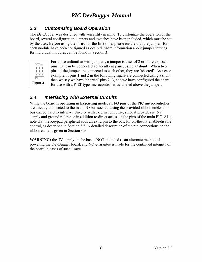
PIC DevBugger Manual 2.3 Customizing Board Operation The DevBugger was designed with versatility in mind. To customize the operation of the board, several configuration jumpers and switches have been included, which must be set by the user. Before using the board for the first time, please ensure that the jumpers for each module have been configured as desired. More information about jumper settings for individual modules can be found in Section 3.
For those unfamiliar with jumpers, a jumper is a set of 2 or more exposed pins that can be connected adjacently in pairs, using a ‘shunt’. When two pins of the jumper are connected to each other, they are ‘shorted’. As a case example, if pins 1 and 2 in the following figure are connected using a shunt, then we say we have ‘shorted’ pins 2+3, and we have configured the board for use with a P18F type microcontroller as labeled above the jumper.
Figure 2
2.4 Interfacing with External Circuits While the board is operating in Executing mode, all I/O pins of the PIC microcontroller are directly connected to the main I/O bus socket. Using the provided ribbon cable, this bus can be used to interface directly with external circuitry, since it provides a +5V supply and ground reference in addition to direct access to the pins of the main PIC. Also, note that the Keypad peripheral adds an extra pin to the bus, for on-the-fly enable/disable control, as described in Section 3.5. A detailed description of the pin connections on the ribbon cable is given in Section 3.9. WARNING: the 5V supply on the bus is NOT intended as an alternate method of powering the DevBugger board, and NO guarantee is made for the continued integrity of the board in cases of such usage.
6 Version 3.0
PIC DevBugger Manual 3. Board Modules
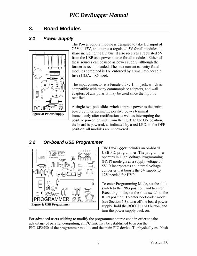
3.1 Power Supply The Power Supply module is designed to take DC input of 7.5V to 17V, and output a regulated 5V for all modules to share including the I/O bus. It also receives a regulated 5V from the USB as a power source for all modules. Either of these sources can be used as power supply, although the former is recommended. The max current capacity for all modules combined is 1A, enforced by a small replaceable fuse (1.25A, TR5 size).
Figure 3: Power Supply
The input connector is a female 5.5×2.1mm jack, which is compatible with many commonplace adaptors, and wall adaptors of any polarity may be used since the input is rectified. A single two-pole slide switch controls power to the entire board by interrupting the positive power terminal immediately after rectification as well as interrupting the positive power terminal from the USB. In the ON position, the board is powered, as indicated by a red LED; in the OFF position, all modules are unpowered.
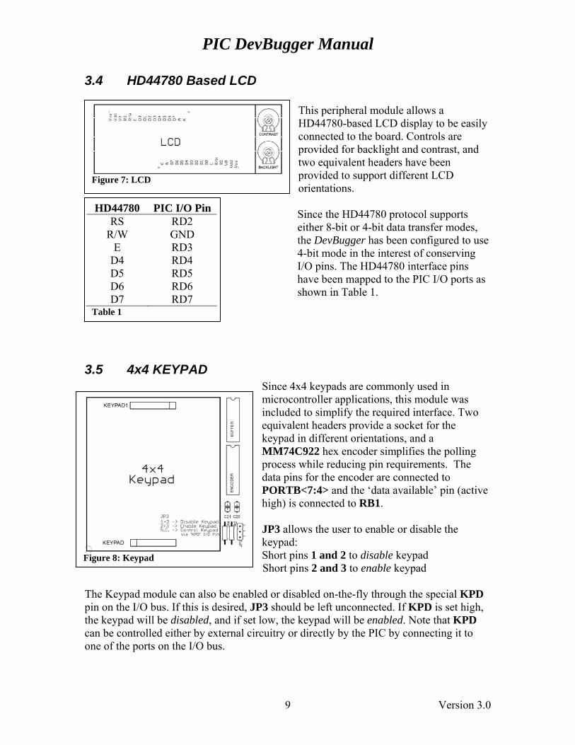
3.2 On-board USB Programmer The DevBugger includes an on-board USB PIC programmer. The programmer operates in High Voltage Programming (HVP) mode given a supply voltage of 5V. It incorporates an internal voltage converter that boosts the 5V supply to 12V needed for HVP.
Figure 4: USB Programmer
To enter Programming Mode, set the slide switch to the PRG position, and to enter Executing mode, set the slide switch to the RUN position. To enter bootloader mode (see Section 5.3), turn off the board power supply, hold the BOOTLOAD button, and turn the power supply back on.
For advanced users wishing to modify the programmer source code in order to take advantage of parallel computing, an I2C link may be established between the PIC18F2550 of the programmer module and the main PIC device. To physically establish
7 Version 3.0

PIC DevBugger Manual the electrical connection between the two devices, jumpers JP14 and JP15 must be shorted. Users who want to use the PIC18F2550’s I/O pins from the main PIC during runtime also need to short jumpers JP14 and JP15. This function also makes use of the I2C bus implemented on the DevBugger board between the main PIC and the programmer PIC. Please refer to Section 6.2 for more information on these capabilities.
3.3 Debugging Module The Debugging module allows the user to monitor the states of the I/O pins of the main PIC device via 32 indicator LEDs. These indicators are fully buffered, so they do not impact the voltage levels of the signals they are monitoring – in other words, they can safely monitor the logic states of low-power sensor signals. However, it should be noted that unless specific lines are connected to signals or driven by the I/O ports, their indicators may flash unpredictably since they are floating.
Figure 5: Indicator LEDs
The indicators can be disabled in four columns through the included DIP switch, in order to reduce current draw.
To control the LEDs (refer to Figure 5):
Figure 6: Signal Switches
Slide switch 1 for PORTA/PORTE Slide switch 2 for PORTB Slide switch 3 for PORTC Slide switch 4 for PORTD
The DevBugger also comes with 32 DIP switches to provide input to the pins of the main PIC for debugging purposes. Each switch corresponds to an indicator LED. Each DIP switch has 3 states – 5V, Ground, and Disconnected. The middle position of each switch disconnects it from its corresponding pin. The user can choose to set each pin high or low by switching the switch to its corresponding state.
8 Version 3.0
PIC DevBugger Manual 3.4 HD44780 Based LCD
This peripheral module allows a HD44780-based LCD display to be easily connected to the board. Controls are provided for backlight and contrast, and two equivalent headers have been provided to support different LCD orientations.
Figure 7: LCD
HD44780 PIC I/O Pin RS RD2
R/W GND E RD3
D4 RD4 D5 RD5 D6 RD6 D7 RD7
Table 1
Since the HD44780 protocol supports either 8-bit or 4-bit data transfer modes, the DevBugger has been configured to use 4-bit mode in the interest of conserving I/O pins. The HD44780 interface pins have been mapped to the PIC I/O ports as shown in Table 1.
3.5 4x4 KEYPAD Since 4x4 keypads are commonly used in microcontroller applications, this module was included to simplify the required interface. Two equivalent headers provide a socket for the keypad in different orientations, and a MM74C922 hex encoder simplifies the polling process while reducing pin requirements. The data pins for the encoder are connected to PORTB<7:4> and the ‘data available’ pin (active high) is connected to RB1.
Figure 8: Keypad
JP3 allows the user to enable or disable the keypad: Short pins 1 and 2 to disable keypad Short pins 2 and 3 to enable keypad
The Keypad module can also be enabled or disabled on-the-fly through the special KPD pin on the I/O bus. If this is desired, JP3 should be left unconnected. If KPD is set high, the keypad will be disabled, and if set low, the keypad will be enabled. Note that KPD can be controlled either by external circuitry or directly by the PIC by connecting it to one of the ports on the I/O bus.
9 Version 3.0

PIC DevBugger Manual 3.6 RS-232 DB-9 Communication
This peripheral module allows the user to communicate with a PC through a serial port, using the PIC’s USART module. A MAX232 chip is used as a level converter since the USART and the serial port use different voltage levels, and a built-in DB9 connector allows easy connection to other RS232-compatible devices. Note that this module is connected to pins RC6 and RC7 when enabled.
Figure 9: RS232 Module To enable this module, short JP10.
3.7 A2D Reference The DevBugger has been equipped with two potentiometers, R12 and R13 to set the voltage reference levels for the Analog to Digital Converter (ADC). To enable these references, short JP4 and JP5; if left unconnected, the references are disabled.
Figure 10: A2D
Short JP4 to enable Vref on RA2 Short JP5 to enable Vref on RA3
3.8 Real Time Clock A Real Time Clock (RTC) and disk battery allow for off-chip timekeeping, even when the rest of the board is unpowered. The circuit is designed for a DS1307 RTC chip, interfaced through I2C on pins RC3 and RC4. To enable, short JP6 and JP7.
Figure 11: RTC
Note 1: The DS1307, 3V lithium disk battery, and jumper shunts are not included with the board. Note 2: The RTC module was designed to be used with backup power (the 3V disk battery) and therefore must have the battery in the socket to ensure consistent operation.
3.8.1 Using the Real Time Clock The DS1307 real time clock can be used to keep track of times in seconds, minutes, hours, days, months, and years. The numbers of days in months are automatically adjusted, including leap years. The hours function allows the chip to keep time in either 12 or 24 hour format with AM/PM indicator for 12 hour format. The advantage of the off-chip timekeeping functionality of the RTC is to free the microcontroller from the task so that it may focus on other tasks. For more detail on the DS1307 real time clock, please refer to Chapter 7 of the AER201 course notes.
10 Version 3.0

PIC DevBugger Manual The RTC communicates with the main PIC microcontroller through the I2C protocol and acts as a slave device with a 7-bit address of 1101 000X (where X denotes if the transaction is a read or a write). In order to use the RTC, the main PIC must be configured as a MSSP device or master device for I2C. The master device is responsible for initiating and controlling the clock pulse for all slave devices, including the RTC. The configuration code for I2C is available to students as two files: i2c_common.asm and rtc_macros.inc. Note that these two files were written for PIC16 devices. Users may modify the source code in order to use these files for PIC18. i2c_common.asm: This source file contains the lowest level algorithm to deal directly with the I2C protocol. It also contains the algorithm to deal with communication between the microcontroller and RTC as well as for the PIC-to-PIC I2C communication. This file must be included in the user’s MPLAB project. rtc_macros.inc: This file must be included in the MPLAB project as well as the user code wherever these macros are called. This file contains three primary macros that can access all the timekeeping functions of the RTC. These are: Macro: rtc_resetAll Input parameters: none Output: none
Description: When invoked, this macro resets all the time keeping registers on the RTC memory or resets time to zero.
Macro: rtc_set address , data
Input parameters: Takes in 2 literal parameters, the address of the register being written to and the data which will be written Output: none Description: This macro will initiate a write event to the RTC. The user must specify the address which will be written to (i.e. the seconds register which holds the time in seconds) and the data which will be written to the specified address.
Macro: rtc_read address Input parameters: address to be read from Output: DOUT (0x75), dig10 (0x77), dig1 (0x78)
Description: This macro will initiate a read event to the RTC and read data from the specified address. The data from the RTC will be saved to data memory general purpose register 0x75 or DOUT as an 8-bit binary number. For the convenience of the user, this data will also be converted into a two digit ASCII number and the tens digit will be stored in 0x77 or dig10 and the ones digit will be stored in 0x78 or dig1. This is advantageous because HD447780 based LCDs only display ASCII numbers.
11 Version 3.0
PIC DevBugger Manual In order to use these files, simply add them to your existing MPLAB project (If you do not know how to make a project in MPLAB, use the MPLAB Project Wizard under Project to generate a project). To do this, follow these steps:
1. Copy i2c_common.asm and rtc_macros.inc into your project directory. 2. Open MPLAB and load the project where the RTC is to be used. 3. Go to View and make sure Project is checked. 4. In the Project window where all the files in the project are listed. Right click
Source File and select Add Files… Select and add i2c_common.asm in your project directory.
5. In the Project window where all the files in the project are listed. Right click Header Files and select Add Files… Select and add rtc_macros.inc in your project directory.
6. In any source files in which the user code calls the RTC macros, you must use the include directive at the top of the page to include rtc_macros.inc. Simply type at the top: include <rtc_macros.inc>.
7. Before using the RTC macros, you must enable and configure the main PIC as a master I2C device. To do this, simply call i2c_common_setup subroutine (this subroutine is located in i2c_common.asm). Simply type: call i2c_common_steup. It is suggested that this subroutine to be called at the top of the main source file. You only need to call this subroutine once.
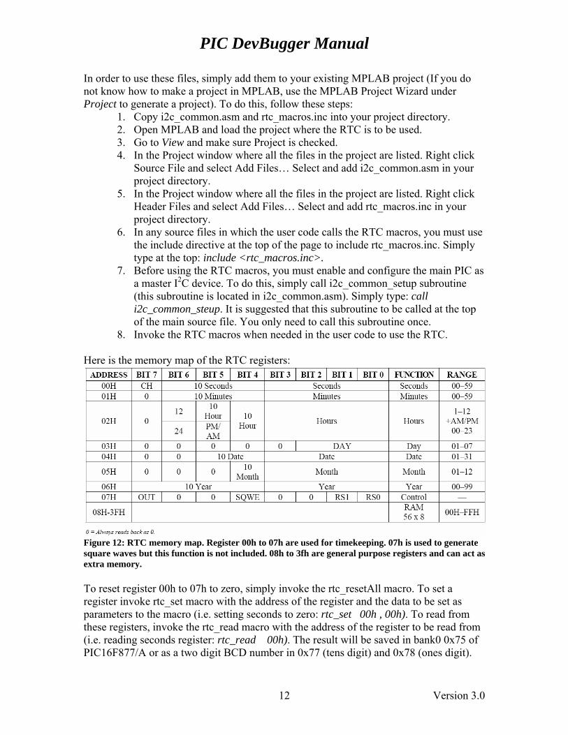
8. Invoke the RTC macros when needed in the user code to use the RTC. Here is the memory map of the RTC registers:
Figure 12: RTC memory map. Register 00h to 07h are used for timekeeping. 07h is used to generate square waves but this function is not included. 08h to 3fh are general purpose registers and can act as extra memory. To reset register 00h to 07h to zero, simply invoke the rtc_resetAll macro. To set a register invoke rtc_set macro with the address of the register and the data to be set as parameters to the macro (i.e. setting seconds to zero: rtc_set 00h , 00h). To read from these registers, invoke the rtc_read macro with the address of the register to be read from (i.e. reading seconds register: rtc_read 00h). The result will be saved in bank0 0x75 of PIC16F877/A or as a two digit BCD number in 0x77 (tens digit) and 0x78 (ones digit).
12 Version 3.0
PIC DevBugger Manual 3.9 Main I/O BUS
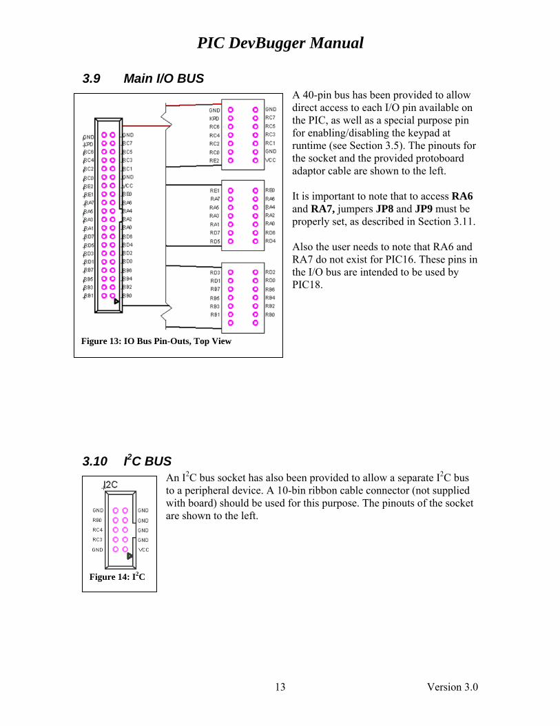
A 40-pin bus has been provided to allow direct access to each I/O pin available on the PIC, as well as a special purpose pin for enabling/disabling the keypad at runtime (see Section 3.5). The pinouts for the socket and the provided protoboard adaptor cable are shown to the left.
Figure 13: IO Bus Pin-Outs, Top View
It is important to note that to access RA6 and RA7, jumpers JP8 and JP9 must be properly set, as described in Section 3.11. Also the user needs to note that RA6 and RA7 do not exist for PIC16. These pins in the I/O bus are intended to be used by PIC18.
3.10 I2C BUS An I2C bus socket has also been provided to allow a separate I2C bus to a peripheral device. A 10-bin ribbon cable connector (not supplied with board) should be used for this purpose. The pinouts of the socket are shown to the left.
Figure 14: I2C
13 Version 3.0

PIC DevBugger Manual 3.11 Main PIC Device This section of the board has several sockets for PIC devices of different sizes. Only one socket may be occupied at a time, otherwise bus conflicts will arise. The DevBugger is primarily intended to be used with a PIC16F877(A) or a PIC18F4620, although most other PIC devices in the PIC16F and PIC18F families are currently supported. Additionally, some PIC16F and PIC18F devices allow the user to employ an internal oscillator and configure RA6 and RA7 as general purpose I/O pins. If this is intended, jumpers JP9 and JP8 must be set as follows:
Figure 15
Short pins 1 and 2 to use external oscillator Short pins 2 and 3 to enable RA6, RA7 Of course, the appropriate configurations must also be set from within the code.
Figure 16: Main PIC Module
14 Version 3.0

PIC DevBugger Manual
4. Programming Software
4.1 Overview A Windows application called PICusb is provided with the DevBugger, which is designed specifically to communicate with the DevBugger hardware. Note that DevBugger is also fully compatible with MPLAB® IDE, and PICusb is not needed (although recommended) except for some advanced applications, such as appending a user code to the firmware on the programmer PIC for parallel processing. PICusb currently supports all devices in the PIC10, PIC12, PIC16 and PIC18 families, and it is compatible with all Windows platforms.
Figure 17: PICusb Application
4.2 Quick Start The user interface for PICusb is fairly intuitive, with reasonable defaults for all settings. For those without prior experience with PIC programming software, the following steps can generally be used to load the HEX code onto the device: 1. Connect the DevBugger to the PC as described in Section 2.2. 2. Flip the programming switch to PRG mode.
15 Version 3.0

PIC DevBugger Manual 3. Turn on the DevBugger. 4. Click “Check Connection” on the PICusb window shown above. Wait for the
application to detect the DevBugger and the PIC device. 5. Click “Import” or go to File Import Hex to load a HEX file. 6. Press the Write button to download the HEX file to the PIC device. If no error
message occurs, then the PIC should have been programmed successfully.
Note if the USB connection is disconnected at any point or the programming switch is flipped to RUN mode, the DevBugger must be reconnected to the application by pressing the “Check Connection” button before programming.
Any time that the “Check Connection” button is pressed, the HEX file must be reloaded.
4.3 Operations The following is a description of common operations that may be performed upon the PIC device used in the DevBugger. Import loads a HEX file into memory, for loading onto a PIC device or for verification against the code already loaded onto a PIC device.
Read is used to read the current program loaded into the target PIC device. This program can be retrieved and stored in a HEX file.
Write programs the currently loaded HEX code into the target device. Several options for this operation are available. By default, all aspects of the HEX file are programmed into the device; however, checkboxes in the Program Memory tab and the EEPROM Memory tab can allow sections of the HEX file to be programmed.
Verify reads the contents of the PIC device and compares it against the loaded HEX file. If any differences are observed, an error is given and the operation fails.
Erase performs a bulk erase of the device, effectively returning it to its factory state. In some cases, this may fix a device that appears faulty.
Check Blank is used to verify that the chip is indeed ‘blank’. This is useful after performing an Erase chip operation to verify that the operation succeeded.
4.4 Additional Features of PICusb The PICusb application incorporates a number of additional features designed to increase efficiency and speed up the code development process as well as to provide advanced functionality.
Write after Import: This checkbox, when checked, will automatically download the code onto the target PIC device after a successful import. The user will no longer have to manually press the Write button.
Update HEX Automatically: When this checkbox is first checked, it prompts the user to load a HEX file to download to the PIC. After the code is downloaded, the PICusb
16 Version 3.0
PIC DevBugger Manual application continuously monitors that HEX file. If the HEX file is modified in any way (if the HEX file was updated after a successful build in MPLAB), PICusb detects this change and automatically writes the new updated version onto the PIC. This function will continue to work as long as the programming switch is set to PRG and the USB connection is not severed. This is a useful debugging feature for users who are programming the PIC multiple times in succession. After the code is downloaded, the user may test the code without flipping the programming switch to RUN mode using the Set MCLR function. The only drawback is that the bottom two rows of the keypad will be disabled in this mode.
Set MCLR: This function is a software reset for the target PIC. It is useful when debugging and especially when used with the Update HEX Automatically function. This feature allows the code on the main PIC to run without flipping the programming switch to RUN mode. When checked, the PIC18F2550 programmer PIC holds the main PIC in a reset state. When unchecked, the programmer releases the reset and the main PIC device will begin to execute code. Note that this reset, when the programming switch is set to PRG, will override the pushbutton reset switch. This function can also be reached from Programmer Hold Device in Reset.
Export Hex: This function, located under the File menu, allows the user to save the HEX code currently loaded onto PICusb into a HEX file. To check what HEX code is currently loaded onto PICusb, go to the Program Memory or EEPROM Memory tabs. This feature is mainly used in conjunction with the Read function for saving the HEX code read from the PIC device into a file.
Recent Files: PICusb preserves the 4 most recently loaded HEX files for faster access under the File menu.
Manual Device Select: This function is used for some PIC10 and PIC12 devices that do not support automatic device detection. This function is found under the Programmer menu. Once activated, a device family must be chosen from the Device Family menu and a particular device must be selected from the “Select Part” dropdown box. To exit this mode, a device must be selected.
Enable Code Protect and Enable Data Protect: These two functions are found under the Tools menu. These functions set the configuration data to enable code or data protection. During development, do not enable these features as they may be permanent.
Use VPP First Program Entry: This function is used when the configuration or ID of the target PIC device becomes corrupt and the programmer is unable to identify the device. This function forces the programmer to program the target PIC, which may correct the code on the target PIC.
Append Hex to Firmware: This feature is an advanced peripheral feature of the application that allows custom user code to be added to the programmer firmware. It is used for PIC-to-PIC parallel processing and is further described in section 5.2.1.
17 Version 3.0

PIC DevBugger Manual Download Firmware: This function allows firmware to be downloaded onto the programmer PIC18F2550. The firmware may be the default firmware or a custom firmware modified with custom user code. It evokes the bootloader to allow the PIC18F2550 to program itself. This feature will corrupt the programmer firmware if used improperly and is therefore recommended for advanced users only.
Configuration: This feature allows the user to view the configuration settings for the target PIC device and change them if the user wishes. It does not provide any information about the function of each configuration bit. It is not recommended for most users to change the configuration settings through this function – all configuration settings should be specified in the code. Modifying the configuration settings in this fashion should be done by advanced users only.
View Program Memory and EEPROM Memory: The Program Memory and EEPROM memory are shown in their respective tabs below the menu bar. Once a HEX code is loaded, the contents of the HEX code can be viewed through these tabs. There is an Enable checkbox on each of these panels that is used for enabling writing the HEX code to the PIC. If unchecked, the code will not be downloaded to the target PIC upon pressing the Write button. Only one of the two checkboxes can be unchecked at any time. The user may also modify the HEX code in these tabs, although this is not recommended for most users. The HEX code may be viewed in HEX format or ASCII format.
4.5 Sample Code
The PICusb package contains 12 sample projects, located in the Samples folder where the application is installed. There are two sets of sample codes – one for PIC18F4620 and the other for PIC16F877. Some PIC18 samples may use the internal oscillator block. All the PIC16 samples are assumed to run with a 10MHz crystal oscillator. The samples are described below. PIC16 Samples: DS1307 RTC This project demonstrates the code necessary to interface with the
DS1307 real-time clock IC (not included) on the DevBugger board, using the I2C module of the main PIC device. Also, it demonstrates RS232 usage; the program first resets the RTC’s seconds to zero, and then repeatedly reads the time and transmits over RS232 to a PC. The baud rate is 9600, with 8-bit data and no parity.
Keypad_LCD This project demonstrates the basics of interfacing with the
Keypad and LCD modules of the DevBugger; anything that is typed on the keypad is immediately displayed on the LCD.
18 Version 3.0

PIC DevBugger Manual PortTest This project is a simple test program, which can be used to quickly
verify that MPLAB, PICusb and the programmer module of the board each function correctly. If this program executes correctly, then each of the Debug LED’s should flash sequentially when the board is placed in RUN mode. Note that RA4 on PIC16 devices will not turn on unless pulled up by either a debug switch or an external resistor, since it is an open-drain output.
RS232 This project demonstrates two-way RS232 communications; it
sends a welcome message to the computer, and then repeatedly echoes any data received back to the computer. As with DS1307 RTC, the baud rate used is 9600, with 8-bit data and no parity.
PIC16LCD This is a simple project that displays a message on the LCD. Input Test This is a project designed to test the input switches on the
debugging module. It sets all pins to input so the user can use the DIP switches to control the LEDs on the debugging module.
ADC This is a project that demonstrates the analog to digital conversion
ability of the PIC16. It takes in a voltage input and control the flashing speed of a LED according to that voltage.
Extended I/O This is a project designed to test the I2C bus connection between
the PIC16 and PIC18. It allows PIC16 to toggle RB6 on PIC18 through the I2C bus.
Parallel Processing This is a project designed to demonstrate the parallel processing
ability of the DevBugger board. The PIC16 can be loaded with any ocde while PIC18 will toggle RB6.
PIC18 Samples: A2D This project tests the Analog to Digital converter module on the
PIC18F4620. This sample uses the internal oscillator of the PIC18F4620 and the Phase Locked Loop feature (PLL), which runs at 32MHz.
PWM This projects tests the PWM module of the PIC18F4620. It
generates a 20kHz signal with 50% duty cycle. The signal is output through the CCP2 pin (RC1).
PIC18LCD This project is the same as the PIC16LCD project, except that it
implements an efficient tabling method only possible in PIC18.
19 Version 3.0

PIC DevBugger Manual Port Test PIC18 This project is the same as the PortTest project for PIC16. PIC18LCD_Keypad This project is the same as the Keypad_LCD project. USART This project is the same as the RS232 project.
20 Version 3.0

PIC DevBugger Manual 5. Advanced Programming Topics
5.1 Overview The programmer module is fully functional out of the box, and can be used to program PIC devices of families PIC16F and PIC18F. However, since the module itself is built around a PIC18F2550, it is capable of much more than programming the main PIC device. To take advantage of this untapped potential, several extra features have been implemented to give the user full control over the device. Note that to take advantage of the following features, the parallel processing firmware must be loaded on the PIC18F2550. Bootloader A USB-enabled bootloader has been programmed into the device’s
firmware, allowing the user to re-load the programmer with their own HEX code.
Mode Detect The programming firmware can detect whether the programmer switch is
set to PRG or to RUN, via pin RC7. For more details, see Section 5.2.1. I2C Bus An I2C bus connecting the PIC18F2550 to the main PIC device may be
enabled by shorting JP14 and JP15. This allows communication between the two devices, opening up the possibility of parallel processing.
Figure 18
PIC18 Bus A secondary I/O bus socket has been provided, giving access to the unused pins on the PIC18F2550. The pin-outs for this socket are shown to the right. Since this is an advanced feature of the board, no cable is provided.
5.2 Coding Firmware Modifications There are two options for modifying the programmer module’s firmware:
1. Append user code to the programmer firmware to modify the run-mode behaviour 2. Use another HVP programmer to re-image the entire PIC18F2550 chip
5.2.1 Modifying Run-Mode Using this option, users can append their own code to the original programmer firmware, which will only be run when the board is in RUN mode. It is strongly recommended that the user code is written in Assembly, since the user would have full control over the location and length of the user code. The user code will be inserted into the firmware between location 0x7D70 and 0x7FEF. This means that the user code can be no longer than 640 bytes or 320 instruction words. To insert user code into the existing programmer firmware, follow these steps:
1. Open PICusb and go to Tools -> Append Hex to Firmware.
21 Version 3.0
PIC DevBugger Manual
2. An “Open File” dialog pops up. Select the user code HEX file you would like to insert and click “Open”.
3. A “Save File” dialog pops up. Choose a file name and the directory for the new combined Hex file and click “Save”.
5.2.1.1 Writing the User Code When appending custom user code to the programmer firmware, the user code must be less than 640 bytes or 320 instructions long. The user code must not contain any configuration words. The structure of the user code should be as follows: #include <p18f2550.inc> org 0x7D70 ;begin the user code at address 0x7D70 UserCode ... ... ... end The programmer firmware is built to periodically check pin RC7. When it is cleared, the firmware automatically jumps to program memory location 0x7D70 to execute the user code. To return to programming mode when the programming switch is set, pin RC7 must be checked periodically. This can be done with the following code: UserCode
bsf TRISC, 7 ;set RC7 to input UserLoop … … …
btfss PORTC, 7 ;test RC7 goto UserLoop reset
;goto 0x2000 ;Alternatively, the code may branch to 0x2000, where ;the programmer firmware begins
5.2.1.2 Exporting the User Code Once compiled, the user must export the custom code into the correct format in order to append to the firmware. This is done in MPLAB by the following steps:
1. Go to File->Export… 2. A dialog opens with the title “Export Hex File”. Uncheck Configuration Bits,
EEPROM Memory and User ID. 3. Make sure the Program Memory check box is checked. 4. Set the program memory to start at 0x7D70 and end at address 0x7FEF. Note: the
end address must not exceed 0x7FEF or PICusb will reject the hex file. 5. Under the File Format tab, make sure the format selected is INHX32. 6. Click OK, and save the exported hex file.
22 Version 3.0

PIC DevBugger Manual 5.2.1.3 Loading Modified Firmware onto the PIC18F2550
1. In the PICusb software, select Tools->Download Firmware. 2. A dialog opens. Select the modified (appended) hex file and click “Open”. 3. PICusb will automatically download the new firmware into the PIC18F2550 and
then reset.
5.2.2 Re-Imaging the PIC18F2550 It is possible to use the bootloader to load custom user code onto the PIC18F2550, but the vectors would have to be remapped to begin at 0x2000 (where the programmer firmware begins). Instead, if the user wishes to erase the entire programmer code including the bootloader, a second high voltage programmer (such as another DevBugger) may be used. The DevBugger was designed such that the PIC18F2550 can be programmed without taking it out of its socket. The second row of the PIC18F2550 I/O header, shown on Figure 17, contains all the pins required to program the PIC18F2550. A second header near the programming switch called ICSP_OUT (shown in Figure 19) is the output from the programmer. This header will allow the programmer to program any external PIC. To use this header to program other boards, the basic firmware (without parallel processing) must be loaded onto the PIC18F2550, and the programming switch must be set to “RUN” mode. This disconnects the header from the main PIC on the DevBugger. Furthermore, the same ICSP_OUT header can be used as an input to program the main PIC on the DevBugger as long as the programming switch is set to PRG. The Pin-out of this header from left to write is as follows:
1. VPP/MCLR 2. VDD 3. VSS (GND) 4. ICSPDAT/PGD 5. ICSPCLK/PGC 6. NC
If the user has another high voltage programmer at hand, and wishes to use both PICs as parallel processors, he/she could program the PIC18F2550 using its I/O header and the other PIC using the ICSP_OUT header. This feature demonstrates the versatility of the PIC DevBugger but is highly advanced and not recommended for most users.
5.2.3 User Code Considerations Since the firmware requires a specific set of configuration words (already set), no configuration information should be included in user-compiled code. It may be assumed that the firmware uses the following configuration settings: #pragma config FOSC = HSPLL_HS //HS osc using PLL #pragma config PLLDIV = 5 //20mhz osc #pragma config USBDIV = 2 //USB clk from PLL #pragma config CPUDIV = OSC1_PLL2 //CPU=PLL/2 #pragma config IESO = OFF //Ext osc only #pragma config FCMEN = OFF //No fallback to int-osc #pragma config PWRT = ON //Enable power-up timer
Figure 19
23 Version 3.0
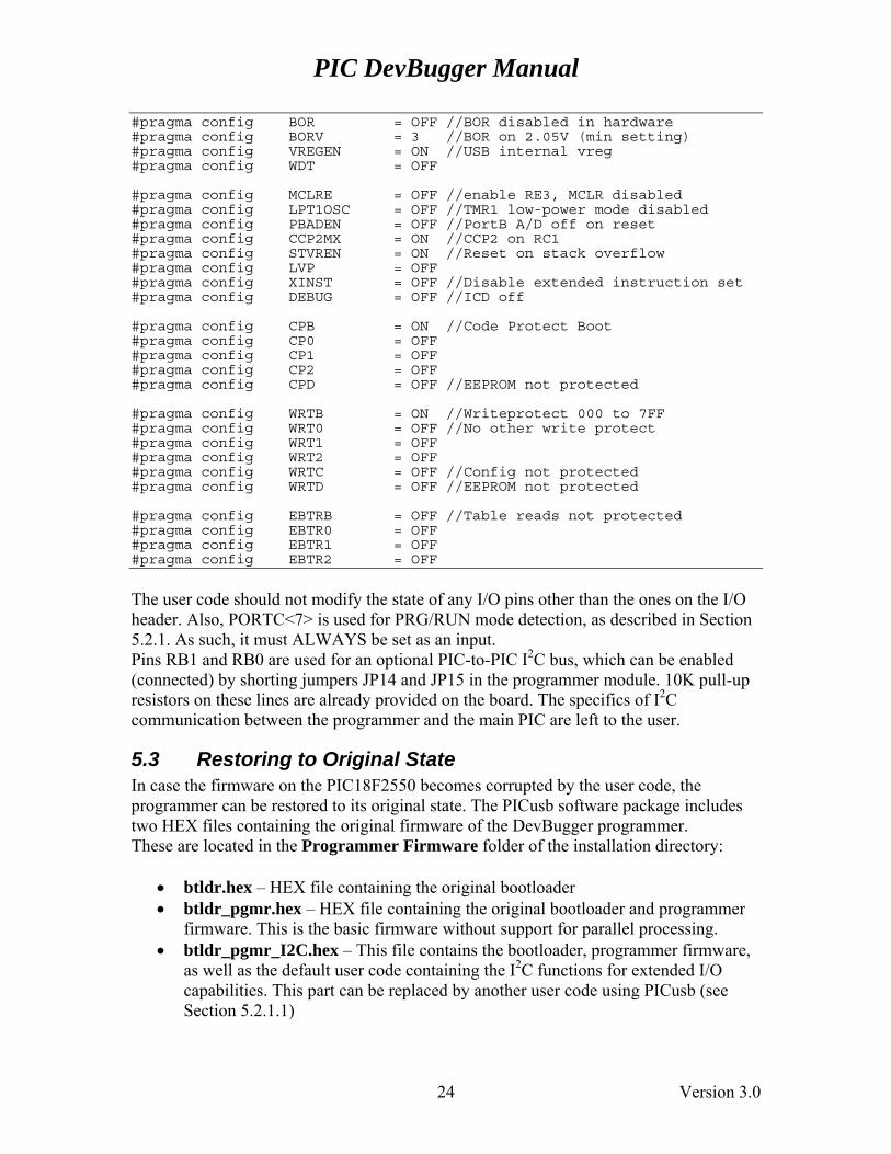
PIC DevBugger Manual #pragma config BOR = OFF //BOR disabled in hardware #pragma config BORV = 3 //BOR on 2.05V (min setting) #pragma config VREGEN = ON //USB internal vreg #pragma config WDT = OFF #pragma config MCLRE = OFF //enable RE3, MCLR disabled #pragma config LPT1OSC = OFF //TMR1 low-power mode disabled #pragma config PBADEN = OFF //PortB A/D off on reset #pragma config CCP2MX = ON //CCP2 on RC1 #pragma config STVREN = ON //Reset on stack overflow #pragma config LVP = OFF #pragma config XINST = OFF //Disable extended instruction set #pragma config DEBUG = OFF //ICD off #pragma config CPB = ON //Code Protect Boot #pragma config CP0 = OFF #pragma config CP1 = OFF #pragma config CP2 = OFF #pragma config CPD = OFF //EEPROM not protected #pragma config WRTB = ON //Writeprotect 000 to 7FF #pragma config WRT0 = OFF //No other write protect #pragma config WRT1 = OFF #pragma config WRT2 = OFF #pragma config WRTC = OFF //Config not protected #pragma config WRTD = OFF //EEPROM not protected #pragma config EBTRB = OFF //Table reads not protected #pragma config EBTR0 = OFF #pragma config EBTR1 = OFF #pragma config EBTR2 = OFF
The user code should not modify the state of any I/O pins other than the ones on the I/O header. Also, PORTC<7> is used for PRG/RUN mode detection, as described in Section 5.2.1. As such, it must ALWAYS be set as an input. Pins RB1 and RB0 are used for an optional PIC-to-PIC I2C bus, which can be enabled (connected) by shorting jumpers JP14 and JP15 in the programmer module. 10K pull-up resistors on these lines are already provided on the board. The specifics of I2C communication between the programmer and the main PIC are left to the user.
5.3 Restoring to Original State In case the firmware on the PIC18F2550 becomes corrupted by the user code, the programmer can be restored to its original state. The PICusb software package includes two HEX files containing the original firmware of the DevBugger programmer. These are located in the Programmer Firmware folder of the installation directory:
• btldr.hex – HEX file containing the original bootloader • btldr_pgmr.hex – HEX file containing the original bootloader and programmer
firmware. This is the basic firmware without support for parallel processing. • btldr_pgmr_I2C.hex – This file contains the bootloader, programmer firmware,
as well as the default user code containing the I2C functions for extended I/O capabilities. This part can be replaced by another user code using PICusb (see Section 5.2.1.1)
24 Version 3.0
PIC DevBugger Manual
• btldr_pgmr_reg_watcher.hex – This file contains the bootloader, programmer firmware, as well as the register watcher code containing the I2C functions for PIC16 pin monitoring ability.
The firmware can be restored by activating the bootloader. This is done by turning off the power switch and holding the BOOTLOAD pushbutton switch while turning the power switch back on. The programmer is in bootloader mode if the BUSY LED flashes at just below 1Hz. The PICusb application will automatically detect that the DevBugger is in bootloader mode. At this time, the original firmware may be downloaded with the Download Firmware function. If the bootloader is corrupt, another high voltage programmer is needed to restore the PIC18F2550 to its original state. The PIC18F2550 can be programmed in circuit through its I/O header as described in section 5.2.2 or taken out of its socket and put on another DevBugger.
25 Version 3.0

PIC DevBugger Manual 6. I2C PIC to PIC Communication
6.1 I2C Overview The I2C is a widely used serial bus specification that allows communication between one or more master devices with one or more slave devices. The master is the device that selects the receiver by transmitting the address of the slave device and initiates all transactions (read or write) between itself and the slave. The I2C implementation on the DevBugger board includes one master – the main PIC – and three slave devices – the RTC chip, the PIC18F2550, and the I2C female header pins at the top right corner of the board which can connect to an external I2C slave device.
6.2 Using the I2C The hierarchical chart below shows the possible applications of the I2C bus, as it is implemented on the DevBugger board.
ApplicationSlave device
Master device
PIC16
RTC chip External timer
PIC18 (programmer)
Parallel processing
PIC18 I/O pin access
PIC16 Pin Monitoring
I2C bus module
Custom application
As shown above, there are four ways in which the I2C bus on the DevBugger can be used. First, one can use access the RTC module for timing purposes through the I2C bus. Second, one can set up PIC-to-PIC communication for parallel processing. This is for advanced users only, as it requires that both the master and the slave be programmed. Third, one can enable PIC-to-PIC I2C communication to enable the usage of PIC18F2550
26 Version 3.0

PIC DevBugger Manual I/O pins by the master PIC during runtime. This effectively adds 7 to the main PIC I/O pin count. Finally, an I2C capable slave device can be connected to the I2C header pins at the top right corner of the board, to communicate with the PIC master device.
6.2.1 PIC-RTC Communication For information on how to use the RTC from the main PIC, please refer to section 3.8.
6.2.2 PIC-to-PIC Communication for Parallel Processing To implement parallel processing, the user must write the necessary code not just for the master PIC device, but also for the PIC18F2550 as the slave device. From the master PIC’s standpoint, programming is greatly simplified by the i2c_common.asm file developed for RTC communication and the extended I/O pin usage protocol. This file is a collection of macros that execute instructions on the hardware level for the I2C – for instance, start transaction, write, check acknowledge, read, send acknowledge, and stop transaction. From the PIC18F2550’s standpoint, the programming is more involved as the user must develop the code from scratch. The slave code polls or waits for an interrupt signaling the start of an event (always initiated by the master device), figures out what type of event it is based on the value of an I2C status register, handles it, and then loops back to the beginning. Microchip’s AN735 and AN734 documents are excellent resources for programming and understanding the I2C protocol, as is Chapter 7 of the AER201 course text, where more detailed information can be found on the I2C.
6.2.3 PIC-to-PIC Extending I/O Set Programming The I2C can be used to enable use of the PIC18F2550’s I/O pins from the main PIC as if they were its own pins. These pins can be controlled using macros available in an include file, which are designed to look and behave similar to regular I/O control operations in the PIC instruction set. This effectively adds 7 additional I/O pins for the master PIC, but the only downside is the roughly 250 μs operation time for write operations and 500 μs for read operations, compared 400 ns for regular operations. Follow the four basic steps below to use the extended I/O pin set:
1. Add i2c_common.asm and p2p_macros.inc to the project (Separate include files are included for PIC18F4620)
2. Add #include <p2p_macros.inc> in the code 3. Add call i2c_common_setup in the code 4. Call the macros as needed
The firmware called btldr_pgmr_I2C.hex is set-up to handle the I/O instructions. This firmware must be loaded into the programmer before the extended I/O set can be used. Below is the list of macros available in the macros include file. The function and usage of these macros do not require explanation as they behave almost identically to their counterparts in the PIC instruction set, except there are no input parameters.
27 Version 3.0
PIC DevBugger Manual
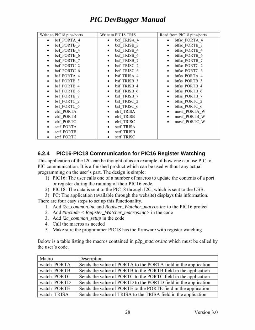
Write to PIC18 pins/ports Write to PIC18 TRIS Read from PIC18 pins/ports • bcf_PORTA_4 • bcf_PORTB_3 • bcf_PORTB_4 • bcf_PORTB_6 • bcf_PORTB_7 • bcf_PORTC_2 • bcf_PORTC_6 • bsf_PORTA_4 • bsf_PORTB_3 • bsf_PORTB_4 • bsf_PORTB_6 • bsf_PORTB_7 • bsf_PORTC_2 • bsf_PORTC_6 • clrf_PORTA • clrf_PORTB • clrf_PORTC • setf_PORTA • setf_PORTB • setf_PORTC
• bcf_TRISA_4 • bcf_TRISB_3 • bcf_TRISB_4 • bcf_TRISB_6 • bcf_TRISB_7 • bcf_TRISC_2 • bcf_TRISC_6 • bsf_TRISA_4 • bsf_TRISB_3 • bsf_TRISB_4 • bsf_TRISB_6 • bsf_TRISB_7 • bsf_TRISC_2 • bsf_TRISC_6 • clrf_TRISA • clrf_TRISB • clrf_TRISC • setf_TRISA • setf_TRISB • setf_TRISC
• btfsc_PORTA_4 • btfsc_PORTB_3 • btfsc_PORTB_4 • btfsc_PORTB_6 • btfsc_PORTB_7 • btfsc_PORTC_2 • btfsc_PORTC_6 • btfss_PORTA_4 • btfss_PORTB_3 • btfss_PORTB_4 • btfss_PORTB_6 • btfss_PORTB_7 • btfss_PORTC_2 • btfss_PORTC_6 • movf_PORTA_W • movf_PORTB_W • movf_PORTC_W
6.2.4 PIC16-PIC18 Communication for PIC16 Register Watching This application of the I2C can be thought of as an example of how one can use PIC to PIC communication. It is a finished product which can be used without any actual programming on the user’s part. The design is simple:
1) PIC16: The user calls one of a number of macros to update the contents of a port or register during the running of their PIC16 code.
2) PIC18: The data is sent to the PIC18 through I2C, which is sent to the USB. 3) PC: The application (available through the website) displays this information.
There are four easy steps to set up this functionality. 1. Add i2c_common.inc and Register_Watcher_macros.inc to the PIC16 project 2. Add #include < Register_Watcher_macros.inc> in the code 3. Add i2c_common_setup in the code 4. Call the macros as needed 5. Make sure the programmer PIC18 has the firmware with register watching
Below is a table listing the macros contained in p2p_macros.inc which must be called by the user’s code. Macro Description watch_PORTA Sends the value of PORTA to the PORTA field in the application watch_PORTB Sends the value of PORTB to the PORTB field in the application watch_PORTC Sends the value of PORTC to the PORTC field in the application watch_PORTD Sends the value of PORTD to the PORTD field in the application watch_PORTE Sends the value of PORTE to the PORTE field in the application watch_TRISA Sends the value of TRISA to the TRISA field in the application
28 Version 3.0
PIC DevBugger Manual watch_TRISB Sends the value of TRISB to the TRISB field in the application watch_TRISC Sends the value of TRISC to the TRISC field in the application watch_TRISD Sends the value of TRISD to the TRISD field in the application watch_TRISE Sends the value of TRISE to the TRISE field in the application watch_register_0 These macros have an input parameter representing the address of
the file register the user wants to monitor. This address is displayed along with the value of the register on the PC application. One can monitor up to 8 registers (registers 0 to 7). Example: watch_register_0 0x05 - The PC application displays 00000101 and the value of
PORTA beside it (0x05 is the address of PORTA).
watch_register_1 watch_register_2 watch_register_3 watch_register_4 watch_register_5 watch_register_6 watch_register_7
There are two things to keep in mind. First, the USB sends a packet every 10 ms, so this is the time-resolution for data updates on the PC application. Secondly, calling one of these macros is a one-time update of the value of the register. For registers with regularly changing values, it is necessary to call the macro repeatedly either in a loop or at crucial junctures in the code. Even so, most of the processing in one’s code takes place in a matter of microseconds since one operation on the PIC16 takes 400 µs – thus, one cannot actually see and monitor the contents of file registers that change this quickly. One solution is to use breakpoints. Using the I2C, it is easy to implement a breakpoint subroutine that stops the PIC16’s operation and waits for the user to press the programmer module’s bootloader switch before continuing. Presented below is the implementation: breakpoint <call whatever watching macros you want here, for e.g. watch_PORTA> bsf_TRISA_0 ; sets the pin the bootloader switch is connected to, to input btfsc_PORTA_0 ; waits for the user to press the switch and pull RA0 low goto $-1 ; if RA0 is not low, keep looping
<put a bit of a delay here> ; so that the PIC is not at the next breakpoint by the time you release the switch
return ; continue with the program The user should call this subroutine at key junctures in the code to stop execution, transmit register values, read them from the PC, and then push the bootloader switch when ready to continue operation.
6.2.5 PIC- I2C Bus Communication Implementing communication between the PIC as the master and an external slave device is for advanced users only. The user would have to program both the master and slave codes, in addition to ensuring that the hardware for the bus connection is set-up properly.
29 Version 3.0

PIC DevBugger Manual
30 Version 3.0
6.3 Important Note About i2c_common.asm and Its Macros The RTC and PIC-to-PIC macros call subroutines in i2c_common.asm and will need to access SFRs on the main PIC. Therefore it will require switching memory banks. Invoking these functions will not guarantee that the user will remain in the same bank after the macros are invoked. It is strongly advised to re-select the memory bank after calling the macros or use the banksel directive in MPLAB®. The i2c_common.asm and the macros are for PIC16F877 and will not work directly with PIC18F4620. However, these files can be ported to PIC18 code with minimal modification. The I2C communication code does take up some of the user’s resources. Since the macros call subroutines, one stack level will be taken. The I2C code will be stored in program memory and will take about 200 to 300 memory slots of the available 8192 slots on the PIC16 without any macro calls. This includes both the real time clock I2C algorithm as well as the PIC-to-PIC algorithm. Keep in mind that macros are simply directives in MPLAB and macro code can be thought of as “copied and pasted” into the user’s code whenever invoked. This will result in the user code being much longer than anticipated especially if these macros are invoked linearly (or not in loops) over and over again. The RTC code will take up 8 general registers in the PIC16 data memory (0x71 to 0x78 in bank0) to store data used during operation. These registers are defined as a cblock in i2c_common.asm and the corresponding names are for convenience sake. The actual code uses the actual register address. The main registers that are relevant to the user are 0x75 (DOUT), 0x77 (dig10), and 0x78 (dig1) where data from the RTC are stored. It is important to not overwrite the data in these registers to ensure proper operation. Likewise, the PIC-to-PIC communication code uses register 0x70, which should not be accessed or modified by the user. Sample code is provided to the students which use i2c_common.asm and rtc_macros.inc as well as p2p_macros.inc.