Physics of Piezoelectric Shear Mode Inkjet Actuators9351/FULLTEXT01.pdf · Physics of Piezoelectric...
109
Physics of Piezoelectric Shear Mode Inkjet Actuators J¨ urgen Br¨ unahl Stockholm 2003 Doctoral Dissertation Royal Institute of Technology Condensed Matter Physics
-
Upload
nguyenkhanh -
Category
Documents
-
view
226 -
download
6
Transcript of Physics of Piezoelectric Shear Mode Inkjet Actuators9351/FULLTEXT01.pdf · Physics of Piezoelectric...

Physics of
Piezoelectric Shear Mode Inkjet Actuators
Jurgen Brunahl
Stockholm 2003
Doctoral DissertationRoyal Institute of TechnologyCondensed Matter Physics

Akademisk avhandling som med tillstand av Kungl Tekniska Hogskolan framlaggestill offentlig granskning for avlaggande av teknisk doktorsexamen mandagen den2 juni 2003 kl 10.00 i C1, Electrum, Isafjordsgatan 22, Kungl Tekniska Hogskolan,Stockholm/Kista.
ISBN 91-628-5675-8TRITA-FYS-5289ISSN 0280-316XISRN KTH/FYS/FTS/R--03/5289--SE
© Jurgen Brunahl, 2003
Universitetsservice US AB, Stockholm 2003
Abstract
This thesis describes work on piezoelectric shear mode actuators used in drop-on-demand ink printing applications. These actuators comprise an array of inkchannels micromachined into bulk Pb(ZrxTi1−x)O3 (PZT) ceramics.
During this study, a new pulsed spectroscopic technique was developed to in-vestigate functional properties of a single channel wall of the actuator. The pulsetechnique is based on recording the transient current in response to a short voltagepulse applied to the channel wall. An electric field applied perpendicular to thepolarization will cause a shear motion of the wall. If a voltage pulse with a fastrise time is high enough in amplitude to actuate the wall, it will act like a tuningfork and oscillate at it’s resonant frequencies. Because of the piezoelectric effect,the mechanical oscillations of the wall can be seen as oscillations in the transientcurrent.
Beside the pulsed technique, dielectric spectroscopy, ferroelectric hysteresis looptracing and stroboscopy were used as characterization techniques. The results ob-tained are discussed in respect to temperature dependence, frequency dispersion,ferroelectric fatigue and acoustic resonance modes.
Another field of interest was the temperature inside the actuator. An electriccircuit, based on the voltage divider principle, was built to monitor the ink temper-ature as a function of the printing pattern. ‘Dummy walls’, located at the beginningand the end of the channel wall array, were used as temperature sensing elements.Since the dielectric permittivity of the PZT channel walls depends on temperature,the capacitance of the ‘dummy walls’ changes with temperature. The informationobtained by this measurement technique was used to investigate alternative mate-rials for the passive components of the actuator.
A further part was the development of a new actuator design called a ‘Chevronactuator’. Chevron actuators include an additional PZT layer with polarization inthe opposite direction to the base plate polarization. Thus, the whole channel wallis used as the active part instead of using just the upper half as in the standardactuator. The main advantage of this technique is a reduced power consumptionof the actuator and therefore less heat dissipation.
Different approaches were used to construct Chevron actuators. Experimentsdetermined the efficiency of the actuators and these results were used to makeimprovements. The Chevron actuators were characterized by the above mentionedtechniques and compared with standard Xaar actuators.
ISBN 91-628-5675-8 • TRITA-FYS-5289 • ISSN 0280-316X • ISRN KTH/FYS/FTS/R--03/5289--SE
iii

iv
Preface
The present work in this thesis was carried out at the division of Condensed MatterPhysics (KMF), Laboratory of Solid State Devices, in the Department of Micro-electronics and Information Technology, Royal Institute of Technology (KTH), inStockholm towards a Swedish Doctoral degree from October 1999 to June 2003 andwas funded by XaarJet AB and by the Swedish agency NUTEK.
This thesis is divided into two parts. The first part, Introduction, gives a briefintroduction into the field of inkjet printing. Different inkjet technologies are re-viewed with main emphasize on Xaar -type shear mode actuators. Chapter 2 reviewsthe properties of lead zirconate titanate (PZT), the piezoelectric material Xaar ac-tuators are made of. Chapter 3 describes the characterization techniques we haveused.
The second part, Our research, describes and discusses experiments and newactuator designs in Chapters 4 to 6. Chapter 7 contains a summary of the includedpapers and manuscripts with comments on my participation.
This thesis is based on the following publications, manuscripts andpatents
I. “Dielectric and Pulsed Spectroscopy of Shear Mode PZT Microactuator”Jurgen Brunahl, Alex Grishin, and Sergey KhartsevMat. Res. Soc. Proc. 657, EE4.6 (2000).
II. “Non destructive Pulsed Technique to Characterize Functional Properties ofMicromachined Bulk PZT”J. Brunahl, A.M. Grishin, and S.I. Khartsev3rd Asian Meeting on Ferroelectrics, Hong Kong, December 2000Ferroelectrics 263, 187-192 (2001).
III. “Thermometry Inside Inkjet Actuators”Werner Zapka, Jurgen Brunahl, Onne Wouters, and Mike de RoosProc. DPP 2001, International Conference on Digital Production Printingand Industrial Applications, 392-396, (2001).
v
vi Abstract
IV. “Piezoelectric shear mode inkjet actuator”Jurgen Brunahl, Alex M. Grishin, Sergey I. Khartsev, Carl OsterbergMat. Res. Soc. Proc. 687, B1.4 (2002).
V. “Piezoelectric shear mode drop-on-demand inkjet actuator”Jurgen Brunahl, Alex M. GrishinSensors and Actuators A: Physical, Volume 101, Issue 3, 371-382 (2002).
VI. ““Chevron”-type piezoelectric inkjet actuator”Jurgen Brunahl, Alex M. GrishinProceedings of the 13th IEEE International Symposium on the Applicationsof Ferroelectrics, ISAF, 491-494 (2002).
VII. “Droplet Deposition Apparatus”Werner Zapka, Jurgen Brunahl, Bosse Nilsson, and Mike de RoosXaar Technology Limited, WO Patent no. 02/26500, (2001).
VIII. “Fatigue of shear mode PZT actuator”Vincent Ferrer, Jurgen Brunahl, Alex GrishinManuscript 2003.
The following papers have been published or submitted, but are not included inthis thesis:
I. “Piezoelectric Chevron Inkjet Actuator by In-Process Polarisation Reversal”Jurgen Brunahl, Gerald Richter, Thomas Jager, Werner ZapkaSubmitted to European Meeting on Ferroelectrics EMF 2003, Cambridge,UK.
II. “Depolarisation Damages of Lead Zirconate Titanate (PZT) Ceramics duringMicromachining”Jurgen Brunahl, Gerald Richter, Thomas Jager, Werner ZapkaSubmitted to European Meeting on Ferroelectrics EMF 2003, Cambridge,UK.
III. “Increased Inkjet Printing Frequency From ’Offset Channel’ Printheads”Werner Zapka, Mark Crankshaw, Jurgen Brunahl, Lars Levin, Uwe Her-rmann, and Gotz MunchowSubmitted to NIP19: The l9th international Congress on Digital PrintingTechnologies 2003,New Orleans, USA.

Acknowledgements
First, I would like to thank my supervisors, Prof. Alex Grishin at KTH andDr. Werner Zapka at XaarJet AB, for their professional guidance, constructive crit-icism, and not least for giving me the opportunity to study at the Department ofCondensed Matter Physics.
I would also like to thank Dr. Sergey Khartsev for sharing his knowledge onferroelectrics with me as well as for his generous technical assistance and manyuseful discussions.
Furthermore, I would like to thank XaarJet AB and all colleagues for making allthe equipment available for my work and more important, I am grateful for havingthe possibility to work freely and independently with the appliances. My specialthanks to Jan Eriksson and Mike de Roos.
I would like to thank all the people who joint me during the last years, Wolf-gang Voit, my first roommate, my colleagues at KMF, Peter Johnsson, Soren Kahl,Mats Blomqvist, Vasyl Denysenkov, Jang-Yong Kim and Joo-Hyong Kim, and allthe German students at Xaar, (even though unable to name all, I wish to thankJorrit Rouwe, Gerrit Grunwald and Gotz Munchow) for being such a nice company.Last but not least, I would like to thank Jung-Hyuk Koh and family for their gen-erous hospitality during my Seoul visit.
Ett stort tack till mina kompisar, Eva, Asa, Cissi, Staffan och Christer.
Finally, I want to thank Eva and Clara and my family for their constant en-couragement and support.
vii

viii

Contents
Abstract iii
Preface iv
List of Papers v
I Introduction 3
1 Inkjet Technologies 51.1 History of inkjet technologies . . . . . . . . . . . . . . . . . . . . . 51.2 Continuous inkjet . . . . . . . . . . . . . . . . . . . . . . . . . . . . 61.3 Drop-on-demand inkjet . . . . . . . . . . . . . . . . . . . . . . . . 7
1.3.1 Thermal inkjet . . . . . . . . . . . . . . . . . . . . . . . . . 71.3.2 Piezoelectric inkjet . . . . . . . . . . . . . . . . . . . . . . . 8
1.4 Xaar -type shear mode inkjet actuator . . . . . . . . . . . . . . . . 111.4.1 Design . . . . . . . . . . . . . . . . . . . . . . . . . . . . . . 111.4.2 Drop generation . . . . . . . . . . . . . . . . . . . . . . . . 121.4.3 Manufacturing . . . . . . . . . . . . . . . . . . . . . . . . . 131.4.4 Print resolution . . . . . . . . . . . . . . . . . . . . . . . . . 151.4.5 Geometrical aspects . . . . . . . . . . . . . . . . . . . . . . 16
2 Lead Zirconate Titanate (PZT) ceramics 232.1 History of PZT . . . . . . . . . . . . . . . . . . . . . . . . . . . . . 232.2 Ferroelectricity and dipole structure . . . . . . . . . . . . . . . . . 23
2.2.1 Ferroelectric domains . . . . . . . . . . . . . . . . . . . . . 242.2.2 Polarization and poling . . . . . . . . . . . . . . . . . . . . 262.2.3 Ferroelectric hysteresis . . . . . . . . . . . . . . . . . . . . . 262.2.4 Dielectric permittivity and dielectric loss . . . . . . . . . . 272.2.5 Electromechanical coupling coefficient . . . . . . . . . . . . 282.2.6 Curie temperature . . . . . . . . . . . . . . . . . . . . . . . 28
2.3 Piezoelectricity . . . . . . . . . . . . . . . . . . . . . . . . . . . . . 29
ix
x Contents
2.3.1 Definition of piezoelectric coefficients and directions . . . . 292.3.2 Piezoelectric effect . . . . . . . . . . . . . . . . . . . . . . . 292.3.3 Lead zirconate titanate (PZT) . . . . . . . . . . . . . . . . 302.3.4 Shear mode displacement . . . . . . . . . . . . . . . . . . . 30
3 Characterization techniques 333.1 Dielectric spectroscopy . . . . . . . . . . . . . . . . . . . . . . . . . 333.2 Manual resonance test . . . . . . . . . . . . . . . . . . . . . . . . . 35
3.2.1 Description . . . . . . . . . . . . . . . . . . . . . . . . . . . 353.2.2 Behavior of PZT near mechanical resonance . . . . . . . . . 36
3.3 Pulsed spectroscopy technique . . . . . . . . . . . . . . . . . . . . . 383.4 Ferroelectric hysteresis P-E loop . . . . . . . . . . . . . . . . . . . 403.5 Stroboscope technique . . . . . . . . . . . . . . . . . . . . . . . . . 42
3.5.1 Drop velocity measurement . . . . . . . . . . . . . . . . . . 433.5.2 Drop volume measurement . . . . . . . . . . . . . . . . . . 43
II Our research 45
4 Physical properties of Xaar inkjet actuators 474.1 Temperature dependence of the dielectric properties . . . . . . . . 474.2 Frequency dispersion . . . . . . . . . . . . . . . . . . . . . . . . . . 484.3 Ferroelectric fatigue . . . . . . . . . . . . . . . . . . . . . . . . . . 504.4 Acoustic resonance modes . . . . . . . . . . . . . . . . . . . . . . . 534.5 Correlation with inkjet performance . . . . . . . . . . . . . . . . . 55
5 Thermometry inside inkjet actuators 575.1 Introduction . . . . . . . . . . . . . . . . . . . . . . . . . . . . . . . 575.2 Theoretical background . . . . . . . . . . . . . . . . . . . . . . . . 58
5.2.1 Temperature compensation . . . . . . . . . . . . . . . . . . 585.2.2 Existing temperature compensation . . . . . . . . . . . . . 585.2.3 Temperature dependence of channel wall capacitance . . . . 59
5.3 Experimental setup . . . . . . . . . . . . . . . . . . . . . . . . . . . 615.3.1 Modification of the printhead . . . . . . . . . . . . . . . . . 615.3.2 Electronics . . . . . . . . . . . . . . . . . . . . . . . . . . . 61
5.4 Measurements . . . . . . . . . . . . . . . . . . . . . . . . . . . . . . 625.4.1 Calibration . . . . . . . . . . . . . . . . . . . . . . . . . . . 625.4.2 Temperature differences induced by ink flow . . . . . . . . . 635.4.3 Temperature differences induced by print pattern . . . . . . 63
5.5 Conclusions . . . . . . . . . . . . . . . . . . . . . . . . . . . . . . . 67
Contents xi
6 Chevron-type inkjet actuator 696.1 Introduction . . . . . . . . . . . . . . . . . . . . . . . . . . . . . . . 696.2 Laminated Chevron design . . . . . . . . . . . . . . . . . . . . . . 71
6.2.1 Manufacturing . . . . . . . . . . . . . . . . . . . . . . . . . 716.2.2 Optimization of active layer thicknesses . . . . . . . . . . . 736.2.3 FEM simulations . . . . . . . . . . . . . . . . . . . . . . . . 766.2.4 Influence of glue joint thickness . . . . . . . . . . . . . . . . 776.2.5 Alternative bonding method . . . . . . . . . . . . . . . . . . 77
6.3 Monolithic Chevron design . . . . . . . . . . . . . . . . . . . . . . 786.3.1 Polarization set-up . . . . . . . . . . . . . . . . . . . . . . . 786.3.2 Manufacturing . . . . . . . . . . . . . . . . . . . . . . . . . 806.3.3 Functional performance . . . . . . . . . . . . . . . . . . . . 83
6.4 Conclusions . . . . . . . . . . . . . . . . . . . . . . . . . . . . . . . 85
7 Summary of results 877.1 “Dielectric and Pulsed Spectroscopy of Shear Mode PZT
Microactuator” . . . . . . . . . . . . . . . . . . . . . . . . . . . . . 877.2 “Non destructive Pulsed Technique to Characterize Functional
Properties of Micromachined Bulk PZT” . . . . . . . . . . . . . . . 877.3 “Thermometry Inside Inkjet Actuators” . . . . . . . . . . . . . . . 887.4 “Piezoelectric shear mode inkjet actuator” . . . . . . . . . . . . . . 887.5 “Piezoelectric shear mode drop-on-demand inkjet actuator” . . . . 887.6 ““Chevron”-type piezoelectric inkjet actuator” . . . . . . . . . . . 897.7 “Fatigue of shear mode PZT actuator” . . . . . . . . . . . . . . . . 89
Bibliography 89
Index 93
Papers I - VIII 93
Appendix 93
A PZT piezoelectric materials technical data 97

xii

To Eva and Clara


Part I
Introduction
3

4
Chapter 1
Inkjet Technologies
1.1 History ofinkjet technologies
By 1878, Lord Rayleigh described the mechanism by which a liquid stream breaksup into droplets [1]. However, the first practical inkjet device based on this principlewas patented in 1948 by Siemens Elema in Sweden [2]. In this invention a pressur-ized continuous ink stream was used to record the signal onto a passing recordingmedia. In the early 1960s, R.G. Sweet from Stanford University demonstrated thatby applying a pressure wave pattern, the ink stream could be broken into dropletsof uniform size and spacing [3]. After break-off, electric charge could be impressedon the drops selectively. Whilst the charged droplets, when passed through an elec-tric field, were deflected into a gutter for re-circulation, the remaining unchargeddrops could fly directly onto the media to form an image. This printing process isknown as continuous inkjet. In the 1970s, IBM launched a massive developmentprogramme to adapt continuous inkjet technology to their computer printers [4].
By the late 1970s, the first Drop-on-Demand inkjet methods appeared. A drop-on-demand device ejects ink droplets only when they are needed. Many of the drop-on-demand inkjet systems were invented, developed and produced commercially inthe 1970s and 1980s, e.g. the Siemens PT-80 serial character printer [5]. In theseprinters, on the application of voltage pulses, ink drops are ejected by a pressurewave created by mechanical motions of piezoelectric ceramic actuators.
In 1979, Canon invented a method where ink drops were ejected from the nozzleby the growth and collapse of a water vapor bubble on the top surface of a smallheater located near the nozzle [6]. Canon called this technology Bubble-Jet. Appar-ently at the same time, Hewlett Packard independently developed a similar inkjettechnology and named it ThinkJet (thermal inkjet) [7]. It was the first successfullow-cost inkjet printer based on the bubble jet principle.
5
6 Chapter 1. Inkjet Technologies
Since the late 1980s, thermal inkjet or bubble jet printers have become a vi-able alternative to impact dot-matrix printers for home and office use. This ismainly because of their low cost, small size, quietness, and particularly their colourcapability.
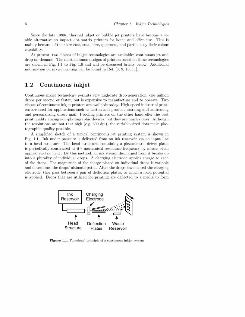
At present, two classes of inkjet technologies are available: continuous jet anddrop-on-demand. The most common designs of printers based on these technologiesare shown in Fig. 1.1 to Fig. 1.6 and will be discussed briefly below. Additionalinformation on inkjet printing can be found in Ref. [8, 9, 10, 11].
1.2 Continuous inkjet
Continuous inkjet technology permits very high-rate drop generation, one milliondrops per second or faster, but is expensive to manufacture and to operate. Twoclasses of continuous inkjet printers are available today. High-speed industrial print-ers are used for applications such as carton and product marking and addressingand personalizing direct mail. Proofing printers on the other hand offer the bestprint quality among non-photographic devices, but they are much slower. Althoughthe resolutions are not that high (e.g. 300 dpi), the variable-sized dots make pho-tographic quality possible.
A simplified sketch of a typical continuous jet printing system is shown inFig. 1.1. Ink under pressure is delivered from an ink reservoir via an input lineto a head structure. The head structure, containing a piezoelectric driver plate,is periodically constricted at it’s mechanical resonance frequency by means of anapplied electric field . By this method, an ink stream discharged from it breaks upinto a plurality of individual drops. A charging electrode applies charge to eachof the drops. The magnitude of the charge placed on individual drops is variableand determines the drops’ ultimate paths. After the drops have exited the chargingelectrode, they pass between a pair of deflection plates, to which a fixed potentialis applied. Drops that are utilized for printing are deflected to a media to form
InkReservoir
ChargingElectrode
HeadStructure
DeflectionPlates
WasteReservoir
Figure 1.1. Functional principle of a continuous inkjet system
1.3. Drop-on-demand inkjet 7
characters while excess drops are directed to a gutter, which in turn directs thedrops to a waste reservoir [12].
1.3 Drop-on-demand inkjet
For drop-on-demand systems, which are microelectromechanical systems (MEMS)that deliver droplets only when needed, several methods of actuating are proposed.Most common is thermoelectric actuation followed by the piezoelectrically drivenactuators. Especially the piezoelectric inkjet technology with its ability to print avariety of fluids is developing in many different directions. Besides printing ink onpaper, new applications can be found in very specific fields such as e.g. biochemistry(DNA printing) or printing of organic polymers, solid particles or adhesives [13, 14,15].
The two most common technologies are thermal inkjet (used by e.g. HewlettPackard and Canon) and piezoelectric inkjet (used by e.g. Xaar, Epson and Brother).
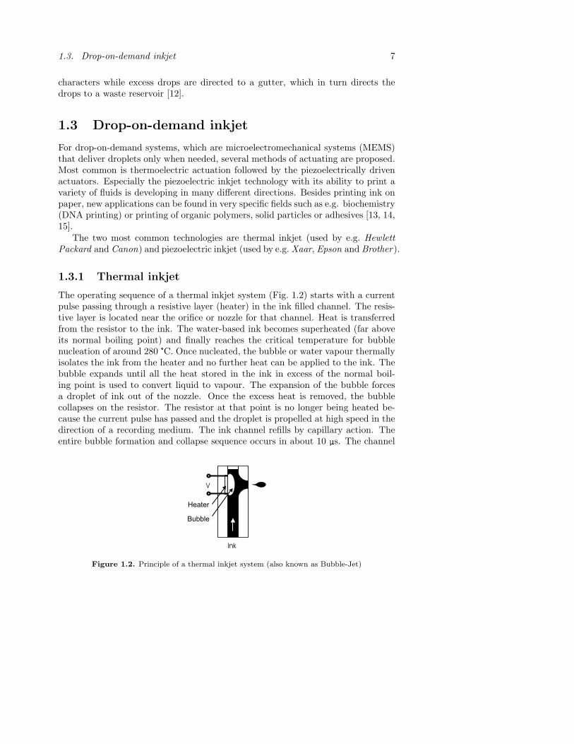
1.3.1 Thermal inkjet
The operating sequence of a thermal inkjet system (Fig. 1.2) starts with a currentpulse passing through a resistive layer (heater) in the ink filled channel. The resis-tive layer is located near the orifice or nozzle for that channel. Heat is transferredfrom the resistor to the ink. The water-based ink becomes superheated (far aboveits normal boiling point) and finally reaches the critical temperature for bubblenucleation of around 280 °C. Once nucleated, the bubble or water vapour thermallyisolates the ink from the heater and no further heat can be applied to the ink. Thebubble expands until all the heat stored in the ink in excess of the normal boil-ing point is used to convert liquid to vapour. The expansion of the bubble forcesa droplet of ink out of the nozzle. Once the excess heat is removed, the bubblecollapses on the resistor. The resistor at that point is no longer being heated be-cause the current pulse has passed and the droplet is propelled at high speed in thedirection of a recording medium. The ink channel refills by capillary action. Theentire bubble formation and collapse sequence occurs in about 10 µs. The channel
Heater
Ink
Bubble
V
Figure 1.2. Principle of a thermal inkjet system (also known as Bubble-Jet)
8 Chapter 1. Inkjet Technologies
can be refired after a 100 to 500 µs minimum dwell time to enable the channel tobe refilled [16].
1.3.2 Piezoelectric inkjet
Piezoelectric inkjet printers harness the inverse piezoelectric effect, which causescertain crystalline materials to change shape when a voltage is applied across them.A small electrical pulse makes the crystal contract slightly, squeezing ink out of thenozzle onto the media.
Depending on the piezoelectric ceramics’ deformation mode, the technology canbe classified into four main types: squeeze, bend, push, and shear. For squeezemode, radially polarized ceramic tubes are used. In both, bend- and push-modedesign, the electric field is generated between the electrodes parallel to the polariza-tion of the piezomaterial. In a shear mode printhead, the electric field is designedto be perpendicular to the polarization of the piezoceramics.
Squeeze mode actuator
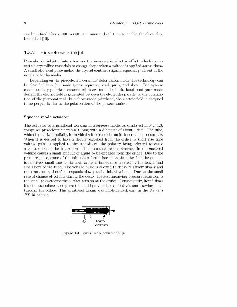
The actuator of a printhead working in a squeeze mode, as displayed in Fig. 1.3,comprises piezoelectric ceramic tubing with a diameter of about 1 mm. The tube,which is polarized radially, is provided with electrodes on its inner and outer surface.When it is desired to have a droplet expelled from the orifice, a short rise timevoltage pulse is applied to the transducer, the polarity being selected to causea contraction of the transducer. The resulting sudden decrease in the enclosedvolume causes a small amount of liquid to be expelled from the orifice. Due to thepressure pulse, some of the ink is also forced back into the tube, but the amountis relatively small due to the high acoustic impedance created by the length andsmall bore of the tube. The voltage pulse is allowed to decay relatively slowly andthe transducer, therefore, expands slowly to its initial volume. Due to the smallrate of change of volume during the decay, the accompanying pressure reduction istoo small to overcome the surface tension at the orifice. Consequently, liquid flowsinto the transducer to replace the liquid previously expelled without drawing in airthrough the orifice. This printhead design was implemented, e.g., in the SiemensPT-80 printer.
Ink
Piezo
Ceramics
Figure 1.3. Squeeze mode actuator design

1.3. Drop-on-demand inkjet 9
Bend mode actuator
Fig. 1.4 shows a piezoelectric inkjet printhead operating in bend mode. It consistsof a pressure chamber including an ink inlet and an outlet passage terminated inan orifice. A conductive diaphragm forms one side of the chamber with a deflectionplate made of piezoelectric ceramic attached. The outer surface of the plate iscovered by a conductive coating, which provides an electrical connection to theplate. Applying a voltage to the piezoelectric plate results in a contraction of theplate thereby causing the diaphragm to flex inwardly into the pressure chamber.This, of course, applies pressure to the printing fluid in the chamber, which forcesa droplet to be expelled from the orifice. The size of the droplets is defined by thevoltage applied to the deflection plate, the pulse duration, and the diameter of theorifice [17]. The printheads in Tektronix ’s Phaser and Epson’s Color Stylus inkjetprinters are based on this design principle.
PiezoCeramics
Ink
Diaphragm
Figure 1.4. Principle of the bend mode technique
Push mode actuator
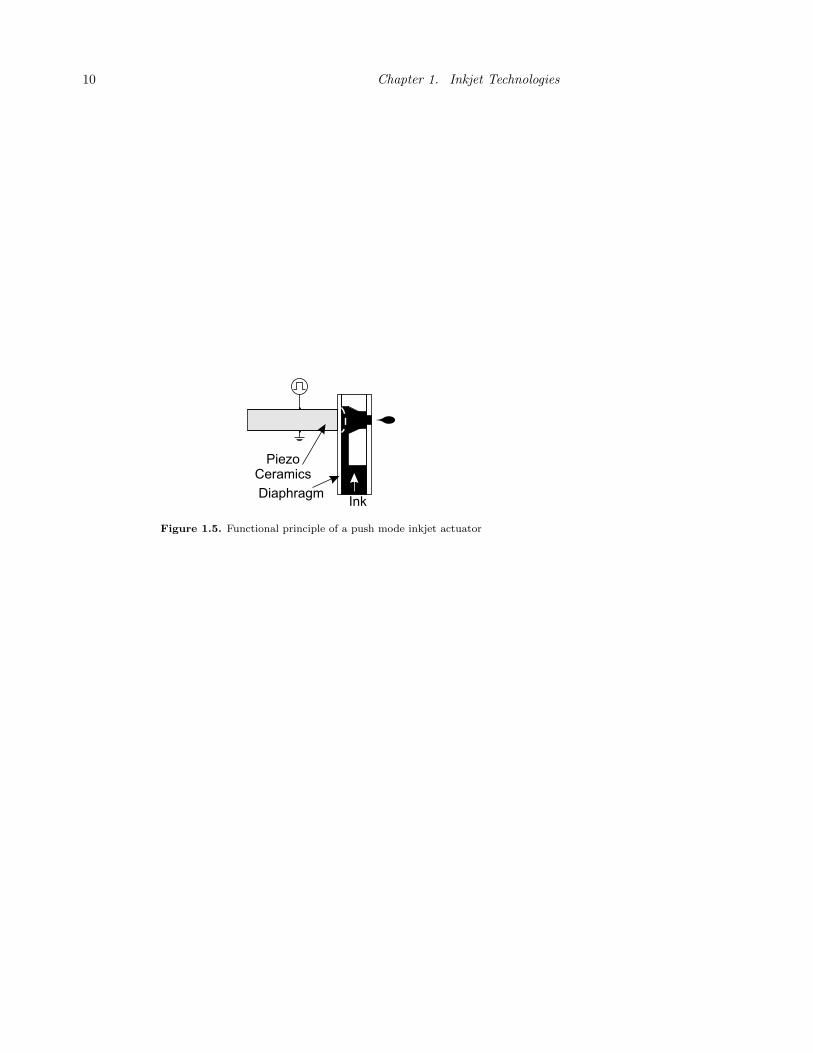
In a push mode design (Fig. 1.5), as the piezoelectric ceramic rod expands, it pushesagainst a diaphragm to eject the droplets from an orifice.
In theory, the piezoelectric actuators can directly contact and push against theink. However, in practical implementation, a thin diaphragm between the piezo-electric actuators and the ink is incorporated to prevent the undesirable interactionbetween ink and actuator materials [18]. Successful implementation of the pushmode piezoelectric inkjet is found in printheads from companies such as DataProd-ucts, Trident, and Epson.
10 Chapter 1. Inkjet Technologies
PiezoCeramics
InkDiaphragm
Figure 1.5. Functional principle of a push mode inkjet actuator
1.4. Xaar-type shear mode inkjet actuator 11
1.4 Xaar-type shear mode inkjet actuator
This chapter describes the design and the functionality of piezoelectric Xaar -typeshear mode inkjet actuators (herein after referred to as ‘actuator ’).
1.4.1 Design
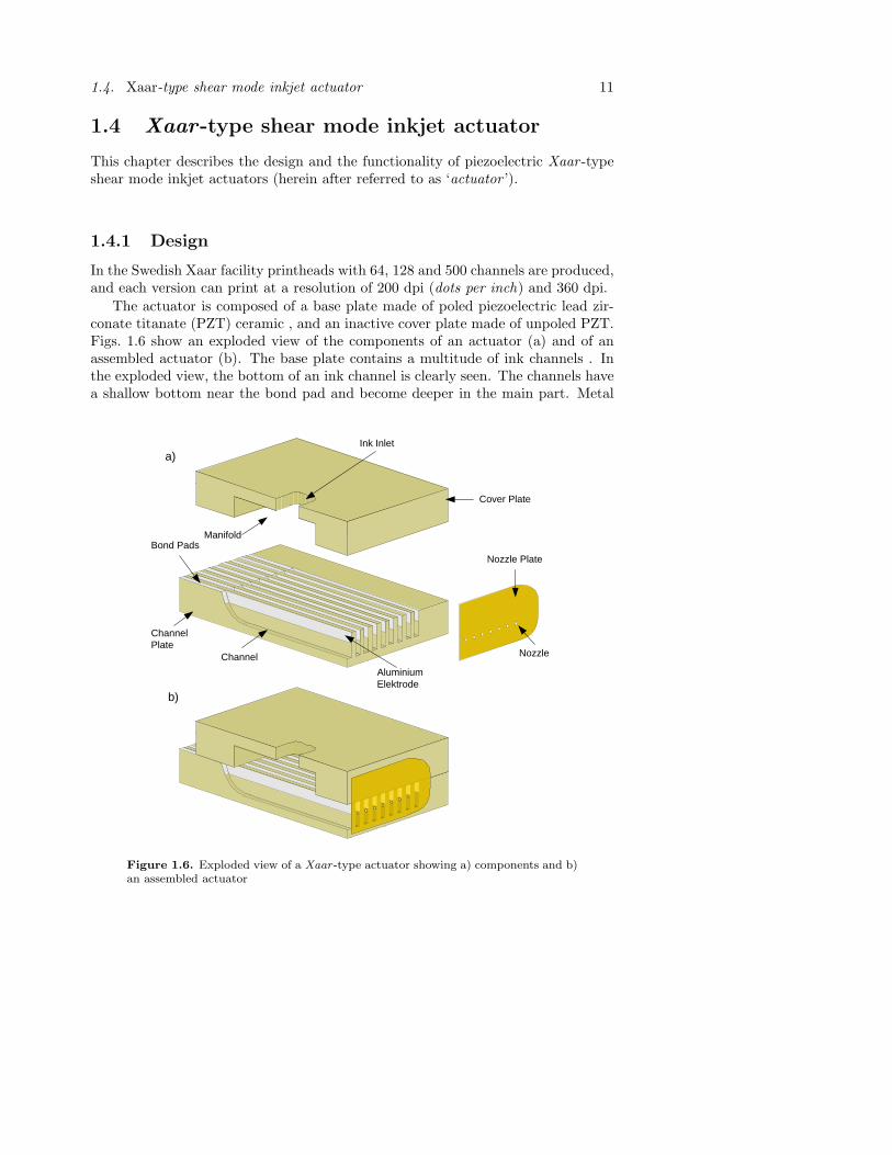
In the Swedish Xaar facility printheads with 64, 128 and 500 channels are produced,and each version can print at a resolution of 200 dpi (dots per inch) and 360 dpi.
The actuator is composed of a base plate made of poled piezoelectric lead zir-conate titanate (PZT) ceramic , and an inactive cover plate made of unpoled PZT.Figs. 1.6 show an exploded view of the components of an actuator (a) and of anassembled actuator (b). The base plate contains a multitude of ink channels . Inthe exploded view, the bottom of an ink channel is clearly seen. The channels havea shallow bottom near the bond pad and become deeper in the main part. Metal
Ink Inlet
Cover Plate
Bond Pads
Channel Plate
Aluminium Elektrode
Channel
Nozzle Plate
Nozzle
Manifold
a)
b)
Figure 1.6. Exploded view of a Xaar -type actuator showing a) components and b)an assembled actuator
12 Chapter 1. Inkjet Technologies
in channel 1
in channel 2
in channel 3
across the wallsof channel 2
draw reinforcesettlingperiod
acoustic period t2 tP
potential V
tP
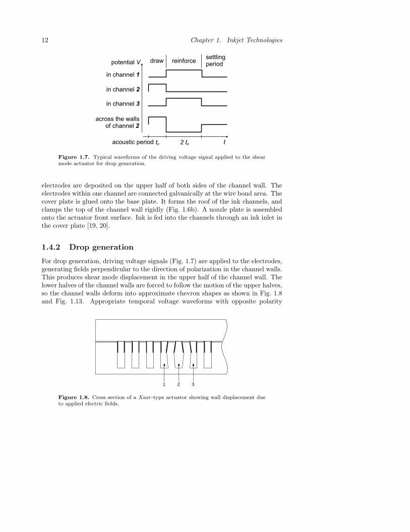
Figure 1.7. Typical waveforms of the driving voltage signal applied to the shearmode actuator for drop generation.
electrodes are deposited on the upper half of both sides of the channel wall. Theelectrodes within one channel are connected galvanically at the wire bond area. Thecover plate is glued onto the base plate. It forms the roof of the ink channels, andclamps the top of the channel wall rigidly (Fig. 1.6b). A nozzle plate is assembledonto the actuator front surface. Ink is fed into the channels through an ink inlet inthe cover plate [19, 20].
1.4.2 Drop generation
For drop generation, driving voltage signals (Fig. 1.7) are applied to the electrodes,generating fields perpendicular to the direction of polarization in the channel walls.This produces shear mode displacement in the upper half of the channel wall. Thelower halves of the channel walls are forced to follow the motion of the upper halves,so the channel walls deform into approximate chevron shapes as shown in Fig. 1.8and Fig. 1.13. Appropriate temporal voltage waveforms with opposite polarity
1 2 3
Figure 1.8. Cross section of a Xaar -type actuator showing wall displacement dueto applied electric fields.
1.4. Xaar-type shear mode inkjet actuator 13
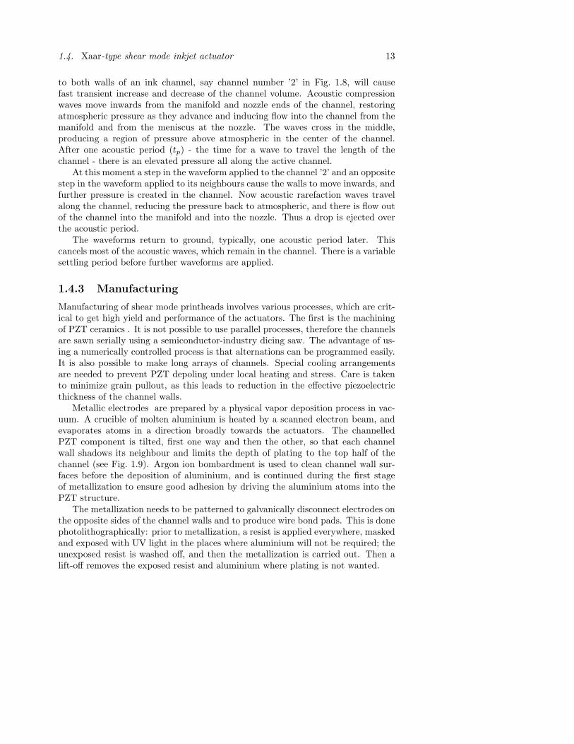
to both walls of an ink channel, say channel number ’2’ in Fig. 1.8, will causefast transient increase and decrease of the channel volume. Acoustic compressionwaves move inwards from the manifold and nozzle ends of the channel, restoringatmospheric pressure as they advance and inducing flow into the channel from themanifold and from the meniscus at the nozzle. The waves cross in the middle,producing a region of pressure above atmospheric in the center of the channel.After one acoustic period (tp) - the time for a wave to travel the length of thechannel - there is an elevated pressure all along the active channel.
At this moment a step in the waveform applied to the channel ’2’ and an oppositestep in the waveform applied to its neighbours cause the walls to move inwards, andfurther pressure is created in the channel. Now acoustic rarefaction waves travelalong the channel, reducing the pressure back to atmospheric, and there is flow outof the channel into the manifold and into the nozzle. Thus a drop is ejected overthe acoustic period.
The waveforms return to ground, typically, one acoustic period later. Thiscancels most of the acoustic waves, which remain in the channel. There is a variablesettling period before further waveforms are applied.
1.4.3 Manufacturing
Manufacturing of shear mode printheads involves various processes, which are crit-ical to get high yield and performance of the actuators. The first is the machiningof PZT ceramics . It is not possible to use parallel processes, therefore the channelsare sawn serially using a semiconductor-industry dicing saw. The advantage of us-ing a numerically controlled process is that alternations can be programmed easily.It is also possible to make long arrays of channels. Special cooling arrangementsare needed to prevent PZT depoling under local heating and stress. Care is takento minimize grain pullout, as this leads to reduction in the effective piezoelectricthickness of the channel walls.
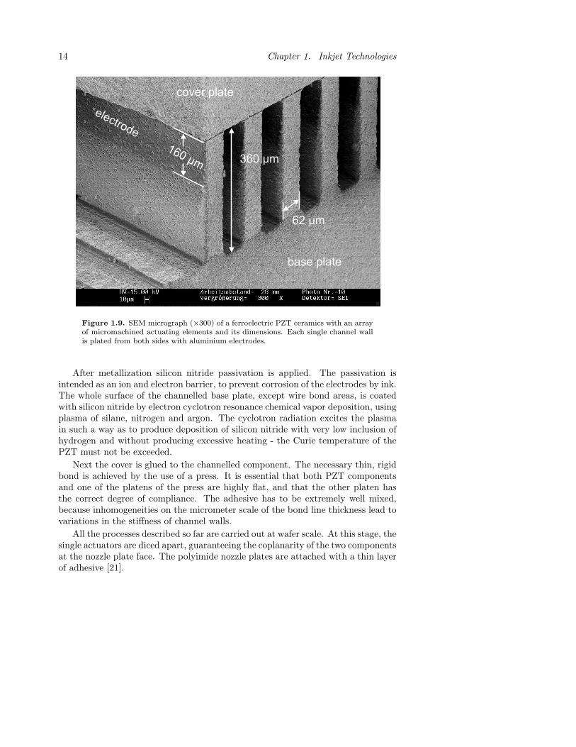
Metallic electrodes are prepared by a physical vapor deposition process in vac-uum. A crucible of molten aluminium is heated by a scanned electron beam, andevaporates atoms in a direction broadly towards the actuators. The channelledPZT component is tilted, first one way and then the other, so that each channelwall shadows its neighbour and limits the depth of plating to the top half of thechannel (see Fig. 1.9). Argon ion bombardment is used to clean channel wall sur-faces before the deposition of aluminium, and is continued during the first stageof metallization to ensure good adhesion by driving the aluminium atoms into thePZT structure.
The metallization needs to be patterned to galvanically disconnect electrodes onthe opposite sides of the channel walls and to produce wire bond pads. This is donephotolithographically: prior to metallization, a resist is applied everywhere, maskedand exposed with UV light in the places where aluminium will not be required; theunexposed resist is washed off, and then the metallization is carried out. Then alift-off removes the exposed resist and aluminium where plating is not wanted.
14 Chapter 1. Inkjet Technologies
electrode
160 µm 360 µm
cover plate
base plate
62 µm
Figure 1.9. SEM micrograph (×300) of a ferroelectric PZT ceramics with an arrayof micromachined actuating elements and its dimensions. Each single channel wallis plated from both sides with aluminium electrodes.
After metallization silicon nitride passivation is applied. The passivation isintended as an ion and electron barrier, to prevent corrosion of the electrodes by ink.The whole surface of the channelled base plate, except wire bond areas, is coatedwith silicon nitride by electron cyclotron resonance chemical vapor deposition, usingplasma of silane, nitrogen and argon. The cyclotron radiation excites the plasmain such a way as to produce deposition of silicon nitride with very low inclusion ofhydrogen and without producing excessive heating - the Curie temperature of thePZT must not be exceeded.
Next the cover is glued to the channelled component. The necessary thin, rigidbond is achieved by the use of a press. It is essential that both PZT componentsand one of the platens of the press are highly flat, and that the other platen hasthe correct degree of compliance. The adhesive has to be extremely well mixed,because inhomogeneities on the micrometer scale of the bond line thickness lead tovariations in the stiffness of channel walls.
All the processes described so far are carried out at wafer scale. At this stage, thesingle actuators are diced apart, guaranteeing the coplanarity of the two componentsat the nozzle plate face. The polyimide nozzle plates are attached with a thin layerof adhesive [21].

1.4. Xaar-type shear mode inkjet actuator 15
1.4.4 Print resolution
Resolution is the basic term used to classify printers and is most commonly ex-pressed by the unit dots per inch (dpi). It denotes the number of clearly resolvedpoints a printhead theoretically can print in a one-inch interval. If two numbers aregiven, the first number indicates the horizontal resolution and the second numberthe vertical resolution, e.g. 1440×720 dpi for an Epson Stylus Color 860 printer. [22]
Typical values of a Xaar XJ128-360dpi printhead are shown in Table 1.1 [23].
Table 1.1. XJ128-360 specifications
Property Typical valueResolution, dpi 360
Firing frequency, kHz 8.3Linear speed, m/s 0.59
Number of channels 128Print width, mm 8.9
The horizontal resolution when head/paper movement is horizontal is definedby the firing frequency of the printhead and the linear speed of its horizontal move-ment. E.g., firing the printhead at its maximum firing frequency of 8.3 kHz with alinear speed of 0.59 m/s results in a horizontal distance between impinging dropsof approximately 70 µm, which corresponds to a resolution of 360 dpi. To achievethe vertical resolution it is necessary to know the number of channels and the printwidth. E.g., 128 channels at a print width of 8.9 mm will result in a vertical dropdistance of approximately 70 µm, which corresponds to a resolution of 360 dpi.The vertical resolution of a printer depends also on the positioning accuracy of themechanical paper feed. Since firing frequency and linear speed can be controlledmuch better than the positioning accuracy of the paper feed, a printers horizontalresolution can be much higher than the vertical resolution.
Three additional parameters are important to maintain the resolution of a print-head: drop volume, drop velocity and angular deviation from the center line of dropejection. The volume of a drop should be sufficient to cover the area defined bythe resolution. E.g., if the resolution is 360 dpi, the area to be covered by onedrop is 70 × 70 µm2. Since the drop area is circular the dot diameter has to beexactly the same value as the diagonal of the area defined by the resolution (forthe example 99 µm). The intersection should be as little as possible as shown inFig. 1.10a. If the volume is too small, the printout looks pale because uncoveredparts of the media are still visible (Fig. 1.10b). If the volume is too big, neighboringspots will merge and the printout looks blurred (Fig. 1.10c). The drop volume ispredefined by channel volume and nozzle diameter and depends also on propertiesof the piezoelectric ceramics. Stronger displacement of the wall results in higherdrop volume.

16 Chapter 1. Inkjet Technologies
a) b) c)
Figure 1.10. Effect of the drop size on paper coverage. a) optimal coverage; b)drops too small; c) drops too big.
Fluctuations of drop velocity strongly influence the horizontal resolution of aprinter. If firing frequency and linear movement of the printhead are constant, thenany difference in drop velocity will change the distance between two neighboringdots on the media. E.g., assuming a drop velocity of 7 m/s and 1 mm distancebetween nozzle and media, the time for a droplet to reach the media is 1/7000 s.At the same time a printhead with a linear speed of 0.59 m/s moves a distance of84 µm. If the drop velocity decreases by 10%, the distance moved by the printheadis 10% lager which is already 12% of dot distance at 360 dpi resolution. Dropvelocity depends very much on properties of the PZT ceramics such as piezoelectriccharge constant d15, magnitude, and direction of the polarization.
Angular deviations from the drop ejection center line cause similar problems asdifferences in drop velocity. Depending on the degree and the direction of the an-gular deviation both horizontal and vertical resolution can be affected. A deviationof 1 degree misplaces a dot by 22 µm, if the distance between the nozzle and mediais 1 mm. These deviations can occur, e.g., if the shape of the nozzle is not optimalor if particles are clogging parts of the channel or nozzle, but they do not dependon the properties of PZT ceramics.
1.4.5 Geometrical aspects
The following considerations on pressure in the channel, effect of wall thicknessand nozzle size are derived by Rolf Kaack and described in his master’s thesis [24]produced at XaarJet AB in July 2001.
Pressure in the channel
The fluid characteristics of the actuator can be derived from the continuityequation
−∮
jdA =dm
dt(1.1)
The left side of the equation describes the mass flow density j flowing into or outoff the surface A of a given system, here the openings of a channel, while the right
1.4. Xaar-type shear mode inkjet actuator 17
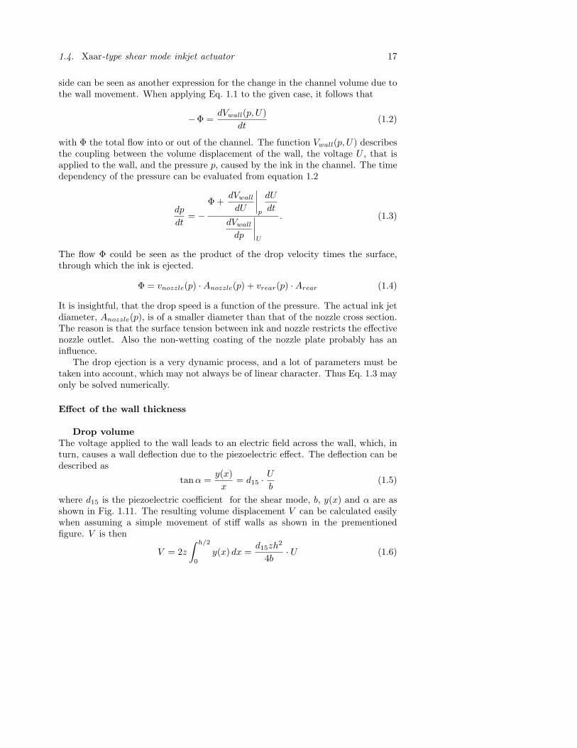
side can be seen as another expression for the change in the channel volume due tothe wall movement. When applying Eq. 1.1 to the given case, it follows that
−Φ =dVwall(p, U)
dt(1.2)
with Φ the total flow into or out of the channel. The function Vwall(p, U) describesthe coupling between the volume displacement of the wall, the voltage U , that isapplied to the wall, and the pressure p, caused by the ink in the channel. The timedependency of the pressure can be evaluated from equation 1.2
dp
dt= −
Φ +dVwall
dU
∣∣∣∣p
dU
dt
dVwall
dp
∣∣∣∣U
. (1.3)
The flow Φ could be seen as the product of the drop velocity times the surface,through which the ink is ejected.
Φ = vnozzle(p) ·Anozzle(p) + vrear(p) ·Arear (1.4)
It is insightful, that the drop speed is a function of the pressure. The actual ink jetdiameter, Anozzle(p), is of a smaller diameter than that of the nozzle cross section.The reason is that the surface tension between ink and nozzle restricts the effectivenozzle outlet. Also the non-wetting coating of the nozzle plate probably has aninfluence.
The drop ejection is a very dynamic process, and a lot of parameters must betaken into account, which may not always be of linear character. Thus Eq. 1.3 mayonly be solved numerically.
Effect of the wall thickness
Drop volumeThe voltage applied to the wall leads to an electric field across the wall, which, inturn, causes a wall deflection due to the piezoelectric effect. The deflection can bedescribed as
tan α =y(x)x
= d15 · U
b(1.5)
where d15 is the piezoelectric coefficient for the shear mode, b, y(x) and α are asshown in Fig. 1.11. The resulting volume displacement V can be calculated easilywhen assuming a simple movement of stiff walls as shown in the prementionedfigure. V is then
V = 2z
∫ h/2
0
y(x) dx =d15zh2
4b· U (1.6)

18 Chapter 1. Inkjet Technologies
F
b
y
x
z
h
y(x)
α
Figure 1.11. Cross section of the wall
Assuming incompressibility of the ink, the ejected ink amount must be as big asthe volume displacement V . Since the ink is ejected through both channel outletsat the nozzle and at the manifold, the volume of the ejected drop, which is equalto the volume that is ejected through the nozzle, depends on the fluidic resistancesRnozzle and Rrear of both openings of the channel. As the walls of a firing channelfirst bend outwards and then inwards, the total Vnozzle must be multiplied by 2.
Vnozzle = 2Rrear
Rnozzle + Rrear· V (1.7)
The fluidic resistances are difficult to describe. At the rear end the pressure of theink in the manifold must also be taken in account.
The effect of the pressure of the ink in the channel has not been taken in accountin the calculation above, because the pulse lengths of the signals, that are applied tothe printhead, are long enough to give the pressure the possibility to equalize or evento become negative. Thus it can be assumed, that the total volume displacement,that can be reached, corresponds to Vnozzle as calculated in Eq. 1.7.
Drop velocityIt can be assumed that the drop velocity is strongly affected by the pressure in
the channel, which in turn depends on the wall width. A reduced wall width leadsto a higher electric field being applied across the wall, which results in a higherpressure in the channel. But the reduced wall width also leads to a lower rigidityof the walls, diminishing the pressure in the channel.
Furthermore, the surface of the rear end of the channel, Arear in Eq. 1.4, in-creases with a thinner wall. Thus it could be, that the effects of the wall width bin the different terms in Eq. 1.3 canceled each other more or less, so that the effectof a thinner wall on drop velocity seems to be quite small.
1.4. Xaar-type shear mode inkjet actuator 19
Effect of the nozzle diameter
Referring to Eq. 1.4, the flow through the nozzle is a function of the surfaceAnozzle(p). It can be seen as the effective surface through which the ink jet isejected. As described above, it does not only depend on the pressure, but is also afunction of the meniscus force and the surface tensions between ink and nozzle. Abigger nozzle diameter leads to a smaller meniscus force and a smaller influence ofthe surface tensions, that, in turn, lead to a higher Anozzle(p).
Finite element method (FEM) simulation
To get an idea of the real shape of the deformed channel wall Finite ElementMethod (FEM) analysis using ANSYS software was performed.
Fig. 1.12 depicts the movement of a non-clamped actuator wall with a heightof 385 µm due to an applied voltage of 22 V, which is the typical driving voltage.Electrode coverage was 43% from the top of the wall.
The shear motion has two components [25], which are also clearly visible in theFEM. The non-clamped wall has its maximum lateral displacement of 14.2 nm atthe top of the wall.
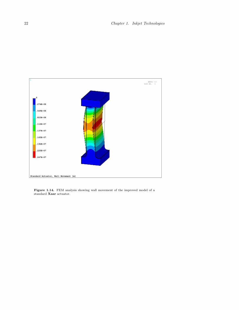
Clamping the wall on the top leads to a change in the shape of the deformation.Both shear motions merge to a single chevron shaped displacement of the wall asdisplayed in Fig. 1.13. The maximum deformation of 26.6 nm is now at the pointwere the electrode ends, approximately 43% from the top. So, clamping the wallat the top doubles the displacement.
Performing resonance analysis on the channel wall model given in Fig. 1.13gave resonance frequencies which where about 16% higher than measured values(for details see Chapter 4). The simplified structure of the model was identifiedas the reason. For better results the model was improved by adding the followingcomponents (depicted in Fig.1.14):
additional PZT bulk material at top and bottom of the channel wall;
glue layer between cover plate and channelled component;
curvature at the bottom of the channel wall;
aluminium (Al) electrodes;
Silicon nitride (SiN) passivation;
Using these improvements it was possible to refine the resonance behavior tomeet real measurements. Table 1.2 shows the percentage affect on the simulatedresonance of the channel wall.
From Table 1.2 we see that including additional PZT bulk material at topand bottom of the channel wall yields values close to real measured data. Allother modifications change the resonance frequency marginally. Therefore, only

20 Chapter 1. Inkjet Technologies
1
Standard Actuator, Wall Movement [m]
0
.157E-08
.314E-08
.472E-08
.629E-08
.786E-08
.943E-08
.110E-07
.126E-07
.142E-07
ANSYS 5.7MAR 18 2003
14:54:59PLOT NO. 1
Figure 1.12. FEM analysis showing wall movement of a non-clamped channel wall
the model with the additional bulk PZT was used for further simulations to keepthe computing time as short as possible.

1.4. Xaar-type shear mode inkjet actuator 21
1
Standard Actuator, Wall Movement [m]
0
.295E-08
.590E-08
.885E-08
.118E-07
.148E-07
.177E-07
.207E-07
.236E-07
.266E-07
ANSYS 5.7MAR 31 2003
12:01:58PLOT NO. 1
Figure 1.13. FEM analysis showing wall movement of a standard Xaar actuator
Table 1.2. Influence of wall components to the resonance behavior of a XJ128-200actuator.
Model resonancefrequency,MHz
deviation inpercent
simplified wall (SW) 1.070 +16SW + Al + SiN 1.100 +20SW + bulk on top and bottom 0.925 +1SW + bulk on top and bottom +glue layer
0.883 -4
SW + bulk on top and bottom +glue layer + curvature
0.895 -3
SW + bulk on top and bottom +glue layer + curvature + Al + SiN
0.915 -1
22 Chapter 1. Inkjet Technologies
1
Standard Actuator, Wall Movement [m]
0
.274E-08
.549E-08
.823E-08
.110E-07
.137E-07
.165E-07
.192E-07
.220E-07
.247E-07
ANSYS 7.0PLOT NO. 1
Figure 1.14. FEM analysis showing wall movement of the improved model of astandard Xaar actuator.

Chapter 2
Lead Zirconate Titanate(PZT) ceramics
2.1 History of PZT
The piezoelectric effect (electricity from applied stress) was first discovered by Pierreand Jacques Curie in 1880. Their experimental demonstration consisted of a con-clusive measurement of surface charges appearing on specially prepared crystals,which were subjected to mechanical stress. In 1881, Gabriel Lippmann deducedmathematically the inverse piezoelectric effect (stress in response to applied elec-tric field). The Curie brothers immediately confirmed the existence of this property.In the following years the 20 natural crystal classes in which piezoelectric effectsoccur and all 18 possible macroscopic piezoelectric coefficients were defined. [26]
Barium titanate (BaTiO3), the first piezoelectric ceramic with perovskite struc-ture, was found around 1943. S. Roberts detected the piezoelectric effect in BaTiO3
in 1947. In 1954, the discovery of the piezoelectric ceramic lead zirconate titanatePb(ZrxTi1−x)O3 (PZT) was reported by B. Jaffe et al.. In the following years PZTbecame the main industrial product in piezoelectric ceramic materials.
Recently, piezoelectric materials in thin film form attracts much attention as akey element for high-frequency surface and bulk acoustic wave devices and microelectromechanical systems (MEMS).
2.2 Ferroelectricity and dipole structure
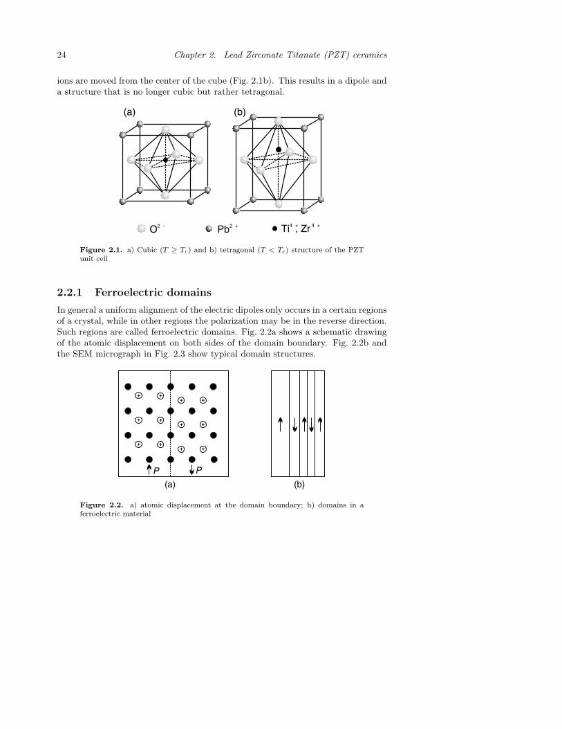
Ceramic perovskites have a cubic (fcc+bcc) structure that is stable at temperaturesabove their Curie temperature (Tc) as seen in Fig. 2.1a. When the temperaturedecreases and falls below Tc the structure changes and in the case of PZT, the O2−
and the Pb2+ -ions are moved from their cubic positions and the Ti4+ and Zr4+
23
24 Chapter 2. Lead Zirconate Titanate (PZT) ceramics
ions are moved from the center of the cube (Fig. 2.1b). This results in a dipole anda structure that is no longer cubic but rather tetragonal.
O2 - Pb2 + Ti , Zr4 + 4 +
(a) (b)
Figure 2.1. a) Cubic (T ≥ Tc) and b) tetragonal (T < Tc) structure of the PZTunit cell
2.2.1 Ferroelectric domains
In general a uniform alignment of the electric dipoles only occurs in a certain regionsof a crystal, while in other regions the polarization may be in the reverse direction.Such regions are called ferroelectric domains. Fig. 2.2a shows a schematic drawingof the atomic displacement on both sides of the domain boundary. Fig. 2.2b andthe SEM micrograph in Fig. 2.3 show typical domain structures.
+
+
+
+
+
+
+
+
+
+
+
+
P P
(a) (b)
Figure 2.2. a) atomic displacement at the domain boundary; b) domains in aferroelectric material
2.2. Ferroelectricity and dipole structure 25
Figure 2.3. SEM micrograph showing domain structure of PZT ceramic

26 Chapter 2. Lead Zirconate Titanate (PZT) ceramics
2.2.2 Polarization and poling
When a ferroelectric ceramic is produced, it shows no piezoelectricity. Because ofthe random orientation of the different grains and the existence of the domains,there is no net polarization. In order for the material to become piezoelectric it hasto be poled.
Poling is the imposition of a DC-voltage across the material. The ferroelectricdomains align to the field resulting in a net piezoelectric effect. Not all the domainsbecome exactly aligned. Some of them align only partially and some do not alignat all. The number of domains that do align depends upon the electric poling field,the temperature and the time the electric field is held on the material. During pol-ing the material permanently increases in dimension between the poling electrodes(Fig. 2.4). The material can be depoled by reversing the poling voltage, increasingthe temperature beyond the Curie temperature or by inducing a large mechanicalstress. [27]
s s'
Strain caused by the field Remanent strain
Figure 2.4. Schematic drawing of the poling process for piezoceramics
2.2.3 Ferroelectric hysteresis
A ferroelectric hysteresis loop for a piezoelectric ceramic is a plot of the polarizationP developed against the field E applied to that device at a given frequency. Atypical hysteresis loop is shown in Fig. 2.5. Applying a small electric field, we onlyget the linear relationship between P and E (1→2), because the field is not largeenough to switch any domain and the sample will behave as a normal dielectricmaterial. As the electric field strength increases (2→3), a number of the negativedomains (which have a polarization opposite to the direction of the field) will beswitched over in the positive direction and the polarization will increase rapidly untilall domains are aligned in the positive direction (4). As the field strength decreases,the polarization will generally decrease but not return back to zero. When the fieldis reduced to zero (5), some of the domains will remain aligned in the positivedirection and the ferroelectric sample will exhibit a remnant polarization Pr. [28]
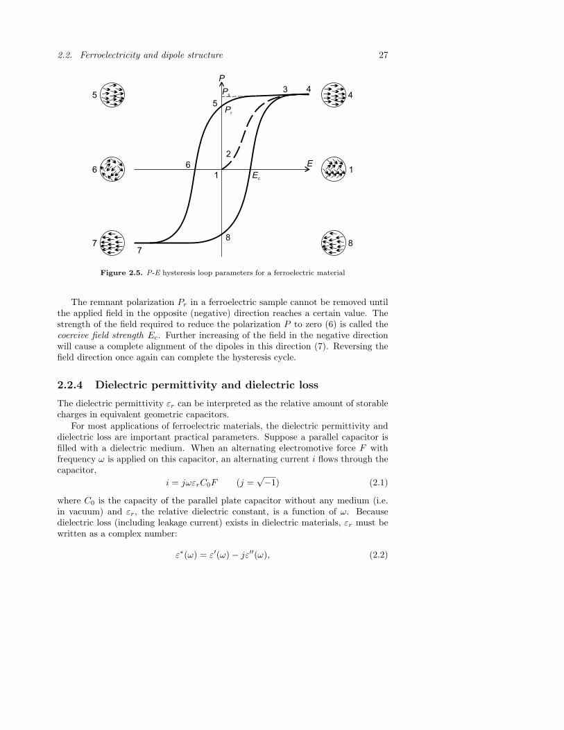
2.2. Ferroelectricity and dipole structure 27
2
1
3 4
5
6
7
8
6
45
87
1 Ec
Pr
Ps
P
E
Figure 2.5. P-E hysteresis loop parameters for a ferroelectric material
The remnant polarization Pr in a ferroelectric sample cannot be removed untilthe applied field in the opposite (negative) direction reaches a certain value. Thestrength of the field required to reduce the polarization P to zero (6) is called thecoercive field strength Ec. Further increasing of the field in the negative directionwill cause a complete alignment of the dipoles in this direction (7). Reversing thefield direction once again can complete the hysteresis cycle.
2.2.4 Dielectric permittivity and dielectric loss
The dielectric permittivity εr can be interpreted as the relative amount of storablecharges in equivalent geometric capacitors.
For most applications of ferroelectric materials, the dielectric permittivity anddielectric loss are important practical parameters. Suppose a parallel capacitor isfilled with a dielectric medium. When an alternating electromotive force F withfrequency ω is applied on this capacitor, an alternating current i flows through thecapacitor,
i = jωεrC0F (j =√−1) (2.1)
where C0 is the capacity of the parallel plate capacitor without any medium (i.e.in vacuum) and εr, the relative dielectric constant, is a function of ω. Becausedielectric loss (including leakage current) exists in dielectric materials, εr must bewritten as a complex number:
ε∗(ω) = ε′(ω)− jε′′(ω), (2.2)
28 Chapter 2. Lead Zirconate Titanate (PZT) ceramics
where ε′(ω) is the real part of the dielectric constant and ε′′(ω) is the imaginarypart. The later represents the dielectric loss. Instead of ε′′, tanδ (tangent of thedielectric loss angle) is most frequently used and can be expressed by:
tanδ =ε′′
ε′(2.3)
2.2.5 Electromechanical coupling coefficient
Electromechanical coupling coefficients k33, k31, kp, and k15 describe the conversionof energy by the ceramic element from electrical to mechanical form or vice versa.The ratio of the stored converted energy of one kind (mechanical or electrical) tothe input energy of the second kind (electrical or mechanical) is defined as thesquare of the coupling coefficient.
k =
√mechanical energy storedelectrical energy applied
or k =
√electrical energy stored
mechanical energy applied(2.4)
Subscripts denote the relative directions of electrical and mechanical quantitiesand the kind of motion involved. They can be associated with vibratory modesof certain simple transducer shapes; k33 is appropriate for a long thin bar, withelectrodes on the ends, polarized along the length, and vibrating in a simple lengthexpansion and contraction. k31 relates to a long thin bar, with electrodes on a pairof long faces, polarized through thickness, and vibrating in simple length expansionand contraction. kp signifies the coupling of electrical and mechanical energy ina thin round disc, polarized through thickness and vibrating in radial expansionand contraction. k15 describes the energy conversion in a thickness shear vibration.Since these coefficients are energy ratios, they are dimensionless. [29]
2.2.6 Curie temperature
An important parameter of ferroelectrics is the temperature of phase transition ,called the Curie temperature Tc. When temperature decreases through the Curietemperature, a ferroelectric crystal undergoes a structural phase transition from aparaelectric phase to a ferroelectric phase. In most ferroelectrics, the temperaturedependence of the dielectric constant can be described by the Curie-Weiss law:
ε′ = ε0
(1 +
W
Tc − T
)(2.5)
where W is the Curie-Weiss constant and T is the temperature.Usually, the temperature independent term ε0 can be neglected, because it is
much smaller than the term εW/(T − Tc) when T is near Tc.
2.3. Piezoelectricity 29
2.3 Piezoelectricity
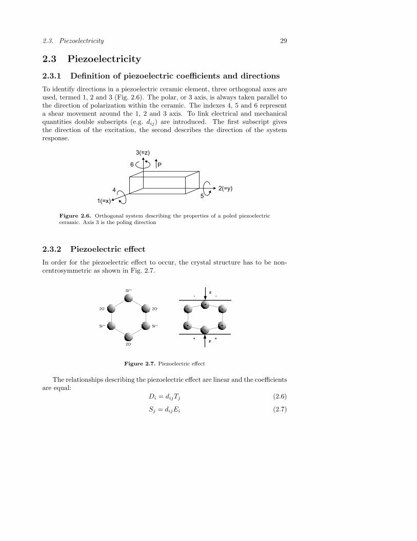
2.3.1 Definition of piezoelectric coefficients and directions
To identify directions in a piezoelectric ceramic element, three orthogonal axes areused, termed 1, 2 and 3 (Fig. 2.6). The polar, or 3 axis, is always taken parallel tothe direction of polarization within the ceramic. The indexes 4, 5 and 6 representa shear movement around the 1, 2 and 3 axis. To link electrical and mechanicalquantities double subscripts (e.g. dij) are introduced. The first subscript givesthe direction of the excitation, the second describes the direction of the systemresponse.
4
1(=x)
3(=z)
2(=y)
6
5
P
Figure 2.6. Orthogonal system describing the properties of a poled piezoelectricceramic. Axis 3 is the poling direction
2.3.2 Piezoelectric effect
In order for the piezoelectric effect to occur, the crystal structure has to be non-centrosymmetric as shown in Fig. 2.7.
Si ++
Si ++ Si ++
2O - 2O -
2O -
-
+ -
+
- +
F
F
- -
+ +
Figure 2.7. Piezoelectric effect
The relationships describing the piezoelectric effect are linear and the coefficientsare equal:
Di = dijTj (2.6)
Sj = dijEi (2.7)
30 Chapter 2. Lead Zirconate Titanate (PZT) ceramics
i = 1, 2, 3 j = 1, 2, 3, 4, 5, 6 ,
in which D is the displacement field (or the charge density), T the applied stress,S is the developed strain and E the applied electrical field.
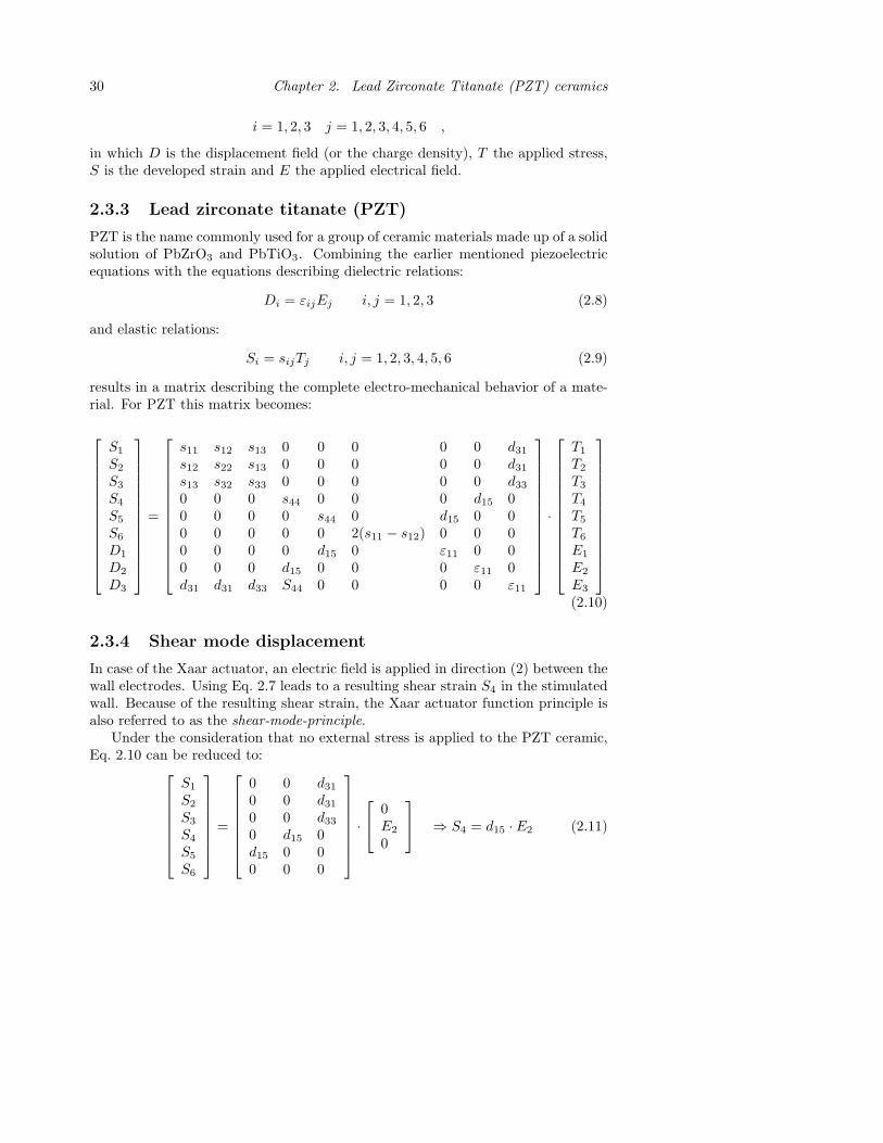
2.3.3 Lead zirconate titanate (PZT)
PZT is the name commonly used for a group of ceramic materials made up of a solidsolution of PbZrO3 and PbTiO3. Combining the earlier mentioned piezoelectricequations with the equations describing dielectric relations:
Di = εijEj i, j = 1, 2, 3 (2.8)
and elastic relations:
Si = sijTj i, j = 1, 2, 3, 4, 5, 6 (2.9)
results in a matrix describing the complete electro-mechanical behavior of a mate-rial. For PZT this matrix becomes:
S1
S2
S3
S4
S5
S6
D1
D2
D3
=
s11 s12 s13 0 0 0 0 0 d31
s12 s22 s13 0 0 0 0 0 d31
s13 s32 s33 0 0 0 0 0 d33
0 0 0 s44 0 0 0 d15 00 0 0 0 s44 0 d15 0 00 0 0 0 0 2(s11 − s12) 0 0 00 0 0 0 d15 0 ε11 0 00 0 0 d15 0 0 0 ε11 0d31 d31 d33 S44 0 0 0 0 ε11
·
T1
T2
T3
T4
T5
T6
E1
E2
E3
(2.10)
2.3.4 Shear mode displacement
In case of the Xaar actuator, an electric field is applied in direction (2) between thewall electrodes. Using Eq. 2.7 leads to a resulting shear strain S4 in the stimulatedwall. Because of the resulting shear strain, the Xaar actuator function principle isalso referred to as the shear-mode-principle.
Under the consideration that no external stress is applied to the PZT ceramic,Eq. 2.10 can be reduced to:
S1
S2
S3
S4
S5
S6
=
0 0 d31
0 0 d31
0 0 d33
0 d15 0d15 0 00 0 0
·
0E2
0
⇒ S4 = d15 · E2 (2.11)

2.3. Piezoelectricity 31
S4 indicates a shear strain around the (1) axis caused by an applied electric fieldin direction (2). As the actuator walls are clamped at both sides (see Fig. 1.8), theshear strain leads to a chevron shaped deflection.

32
Chapter 3
Characterization techniques
For the characterization of the piezoelectric actuators different techniques wereused. Commercial instruments such as Fluke PM6304 RCL-meter and HewlettPackard 4194A Impedance Analyzer are used to measure dielectric permittivity anddielectric losses as functions of frequency and temperature. Tracing of ferroelectrichysteresis P-E loops with a modified Sawyer-Tower circuit was performed to deduceremnant polarizations and coercive fields of the ceramics. To characterize acousticresonance frequencies and electromechanical coupling factors in each of the channelwalls, a novel pulsed technique was employed. Stroboscopic tests were performedto quantify the ultimate inkjet performance: ink-drop velocity, volume, and theirangle deviation.
To investigate temperature dependencies, the specimen was placed into a ther-mostat comprising an oven (a cylindrical metal chamber with heating coils on itsouter surface) and a temperature controller, which regulates the temperature insidethe oven. The actual sample temperature was measured with a Keithley 8 1/2-digitDMM2002 multimeter with built-in linearization for a K-type thermocouple.
To automate the measurements multimeter, temperature controller and mea-surement instrument were connected to a PC via GPIB bus and RS-232 interface.A LabVIEW based routine controls the measurements and saved acquired data intofiles.
3.1 Dielectric spectroscopy
A Fluke PM6304 programmable automatic RCL-meter was used to measure fre-quency and temperature dependencies of dielectric permittivity varepsilon anddielectric loss factor tanδ. The technique is based on simultaneous measurementof the magnitudes of current I, voltage V across the capacitor under test, and therelative phase shift θ between current and voltage. In each measurement cycle thefollowing components are determined:
33
34 Chapter 3. Characterization techniques
Vp = Voltage at 0° Ip = Current at 0°Vq = Voltage at 90° Iq = Current at 90°
From these parameters the following electrical characteristics are calculated:
Impedance:Z = R + iX = |Z|eiφ (3.1)
Resistance:R =
VpIp + VqIq
I2p + I2
q
(3.2)
Reactance:X =
VqIp − VpIq
I2p + I2
q
(3.3)
Quality factor:
Q =|X|R
= tanφ (3.4)
Dielectric loss factor:tanδ =
1Q
=R
|X| (3.5)
Capacitance:
Cp =1
ω(1 + 1/Q2) · |X| if X < 0 (3.6)
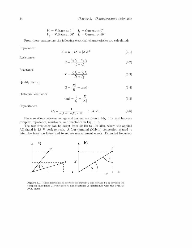
Phase relations between voltage and current are given in Fig. 3.1a, and betweencomplex impedance, resistance, and reactance in Fig. 3.1b.
The test frequency can be swept from 50 Hz to 100 kHz, where the appliedAC-signal is 2.8 V peak-to-peak. A four-terminal (Kelvin) connection is used tominimize insertion losses and to reduce measurement errors. Extended frequency
I
f
V
a)
R
d
Z
X
f
b)
Figure 3.1. Phase relations: a) between the current I and voltage V ; b) between thecomplex impedance Z, resistance R, and reactance X determined with the PM6304RCL-meter.
3.2. Manual resonance test 35
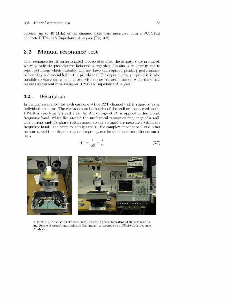
spectra (up to 40 MHz) of the channel walls were measured with a PC/GPIBconnected HP4194A Impedance Analyzer (Fig. 3.2).
3.2 Manual resonance test
The resonance test is an automated process step after the actuators are produced,whereby only the piezoelectric behavior is regarded. Its aim is to identify and toreject actuators which probably will not have the required printing performance,before they are assembled in the printheads. For experimental purposes it is alsopossible to carry out a similar test with uncovered actuators on wafer scale in amanual implementation using an HP4194A Impedance Analyzer.
3.2.1 Description
In manual resonance test each case one active PZT channel wall is regarded as anindividual actuator. The electrodes on both sides of the wall are connected to theHP4194A (see Figs. 3.2 and 3.3). An AC voltage of 1V is applied within a highfrequency band, which lies around the mechanical resonance frequency of a wall.The current and it’s phase (with respect to the voltage) are measured within thefrequency band. The complex admittance Y , the complex impedance Z and othermeasures, and their dependency on frequency, can be calculated from the measureddata.
|Y | = 1|Z| =
I
V(3.7)
Figure 3.2. Shielded probe station for dielectric characterization of the actuator us-ing Quater Research manipulators (left image) connected to an HP4194A ImpedanceAnalyser.
36 Chapter 3. Characterization techniques
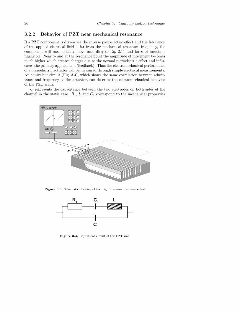
3.2.2 Behavior of PZT near mechanical resonance
If a PZT component is driven via the inverse piezoelectric effect and the frequencyof the applied electrical field is far from the mechanical resonance frequency, thecomponent will mechanically move according to Eq. 2.11 and force of inertia isnegligible. Near to and at the resonance point the amplitude of movement becomesmuch higher which creates charges due to the normal piezoelectric effect and influ-ences the primary applied field (feedback). Thus the electromechanical performanceof a piezoelectric actuator can be measured through simple electrical measurements.An equivalent circuit (Fig. 3.4), which shows the same correlation between admit-tance and frequency as the actuator, can describe the electromechanical behaviorof the PZT walls.
C represents the capacitance between the two electrodes on both sides of thechannel in the static case. R1, L and C1 correspond to the mechanical properties
AC
HP Analyzer
Figure 3.3. Schematic drawing of test rig for manual resonance test
R 1 C 1 L
C
Figure 3.4. Equivalent circuit of the PZT wall

3.2. Manual resonance test 37
of the piezoelectric oscillator: R1 represents the mechanical loss, L the mass andC1 the compliance. The piezoelectric constant and the elastic coefficient of thedrive mode (shear mode in this case) as well as geometry can be seen as a trans-former between real mechanical measurements and the electrical measurements ofthe equivalent circuit. The force corresponds to the voltage and the velocity to thecurrent.
A characteristic curve appears (see Fig. 3.5) when the admittance is plottedversus the frequency.
fs : serial resonance frequency of equivalent circuit (see Fig. 3.4)fp : parallel resonance frequency of equivalent circuitdY : difference of admittance between fs and fp
The coupling coefficient k15 describes the ability of a piezoelectric ceramic totransform electrical into mechanical energy or vice-versa (the index 15 refers to theshear mode; Fig. 2.6) [30]:
k15 =π
2fs
ftan
(π
2fp − fs
fp
)(3.8)
The measured dY and the coupling coefficient k15 can be used to estimate theelectro-mechanical performance of an actuator. The higher the value of k15 andespecially of dY , the better is the performance of the actuator. In the normalmanufacturing process a robot, which measures 64 channel walls at the same time,does this kind of test and an actuator is rejected if dY falls below a certain minimumvalue.
fp
fs
dY
Abs
olut
e ad
mitt
ance
Y, a
.u.
Frequency f, a.u.
Figure 3.5. Admittance behavior of a piezoelectric actuator near its mechanicalresonance.
38 Chapter 3. Characterization techniques
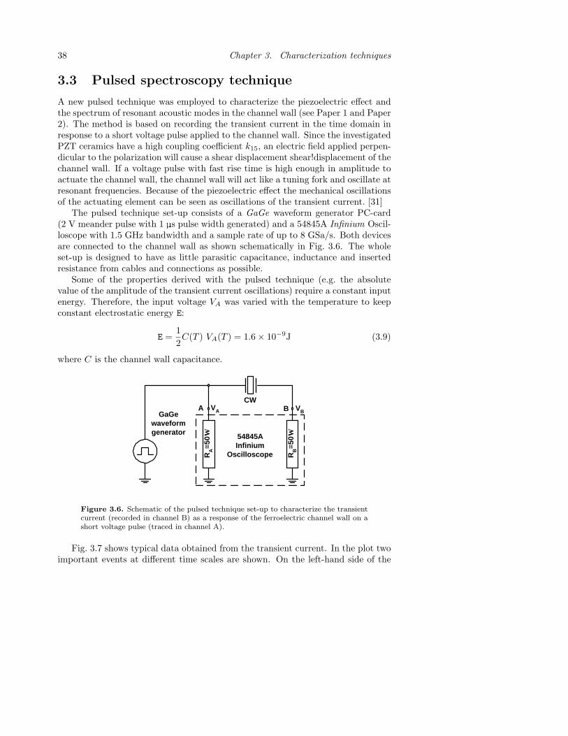
3.3 Pulsed spectroscopy technique
A new pulsed technique was employed to characterize the piezoelectric effect andthe spectrum of resonant acoustic modes in the channel wall (see Paper 1 and Paper2). The method is based on recording the transient current in the time domain inresponse to a short voltage pulse applied to the channel wall. Since the investigatedPZT ceramics have a high coupling coefficient k15, an electric field applied perpen-dicular to the polarization will cause a shear displacement shear!displacement of thechannel wall. If a voltage pulse with fast rise time is high enough in amplitude toactuate the channel wall, the channel wall will act like a tuning fork and oscillate atresonant frequencies. Because of the piezoelectric effect the mechanical oscillationsof the actuating element can be seen as oscillations of the transient current. [31]
The pulsed technique set-up consists of a GaGe waveform generator PC-card(2 V meander pulse with 1 µs pulse width generated) and a 54845A Infinium Oscil-loscope with 1.5 GHz bandwidth and a sample rate of up to 8 GSa/s. Both devicesare connected to the channel wall as shown schematically in Fig. 3.6. The wholeset-up is designed to have as little parasitic capacitance, inductance and insertedresistance from cables and connections as possible.
Some of the properties derived with the pulsed technique (e.g. the absolutevalue of the amplitude of the transient current oscillations) require a constant inputenergy. Therefore, the input voltage VA was varied with the temperature to keepconstant electrostatic energy E:
E =12C(T ) VA(T ) = 1.6× 10⁻⁹J (3.9)
where C is the channel wall capacitance.
CW
GaGe waveform generator
A B
54845A Infinium
Oscilloscope R A
=50 W
R B
=50 W
V A V B
Figure 3.6. Schematic of the pulsed technique set-up to characterize the transientcurrent (recorded in channel B) as a response of the ferroelectric channel wall on ashort voltage pulse (traced in channel A).
Fig. 3.7 shows typical data obtained from the transient current. In the plot twoimportant events at different time scales are shown. On the left-hand side of the
3.3. Pulsed spectroscopy technique 39
0 1 10 20 30
-300
-200
-100
0
100
200
300E
lect
ric
field
E,V/c
m
Timet, ms
-1.5
-1.0
-0.5
0.0
0.5
1.0
1.5V
B[V]=2.7×10
-3exp(-t/10)
VB
E =(VA-V
B)/d
T = 300 K
0115-0755 10/11
VB
×500
Tra
nsi
entsi
gna
lVB
,V
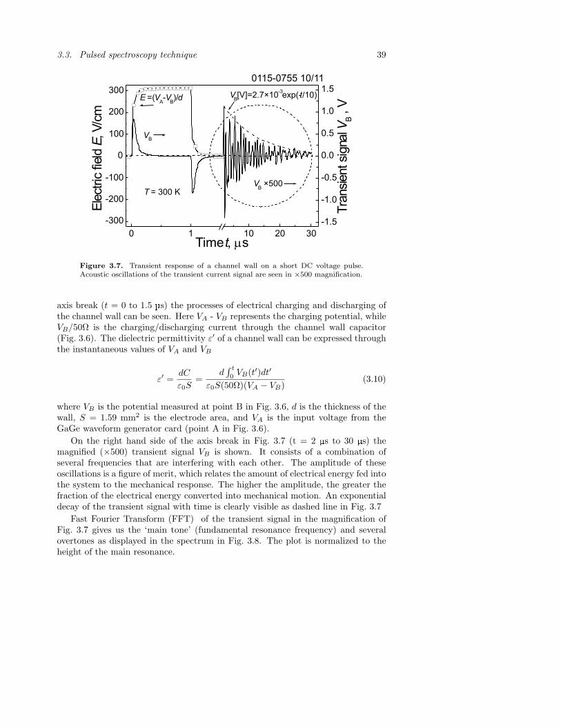
Figure 3.7. Transient response of a channel wall on a short DC voltage pulse.Acoustic oscillations of the transient current signal are seen in ×500 magnification.
axis break (t = 0 to 1.5 µs) the processes of electrical charging and discharging ofthe channel wall can be seen. Here VA - VB represents the charging potential, whileVB/50Ω is the charging/discharging current through the channel wall capacitor(Fig. 3.6). The dielectric permittivity ε′ of a channel wall can be expressed throughthe instantaneous values of VA and VB
ε′ =dC
ε0S=
d∫ t
0VB(t′)dt′
ε0S(50Ω)(VA − VB)(3.10)
where VB is the potential measured at point B in Fig. 3.6, d is the thickness of thewall, S = 1.59 mm2 is the electrode area, and VA is the input voltage from theGaGe waveform generator card (point A in Fig. 3.6).
On the right hand side of the axis break in Fig. 3.7 (t = 2 µs to 30 µs) themagnified (×500) transient signal VB is shown. It consists of a combination ofseveral frequencies that are interfering with each other. The amplitude of theseoscillations is a figure of merit, which relates the amount of electrical energy fed intothe system to the mechanical response. The higher the amplitude, the greater thefraction of the electrical energy converted into mechanical motion. An exponentialdecay of the transient signal with time is clearly visible as dashed line in Fig. 3.7
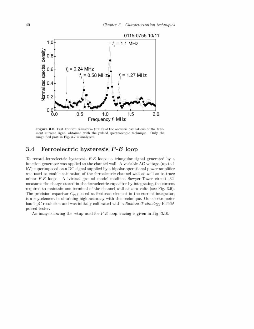
Fast Fourier Transform (FFT) of the transient signal in the magnification ofFig. 3.7 gives us the ‘main tone’ (fundamental resonance frequency) and severalovertones as displayed in the spectrum in Fig. 3.8. The plot is normalized to theheight of the main resonance.
40 Chapter 3. Characterization techniques
0.0 0.5 1.0 1.5 2.00.0
0.2
0.4
0.6
0.8
1.0
0115-0755 10/11
f4= 0.24 MHz
f3
= 0.58 MHz f2= 1.27 MHz
f1
= 1.1 MHz
Frequency f, MHz
Norm
aliz
ed
spectraldensi
ty
Figure 3.8. Fast Fourier Transform (FFT) of the acoustic oscillations of the tran-sient current signal obtained with the pulsed spectroscopic technique. Only themagnified part in Fig. 3.7 is analyzed.
3.4 Ferroelectric hysteresis P-E loop
To record ferroelectric hysteresis P-E loops, a triangular signal generated by afunction generator was applied to the channel wall. A variable AC-voltage (up to 1kV) superimposed on a DC-signal supplied by a bipolar operational power amplifierwas used to enable saturation of the ferroelectric channel wall as well as to traceminor P-E loops. A ‘virtual ground mode’ modified Sawyer-Tower circuit [32]measures the charge stored in the ferroelectric capacitor by integrating the currentrequired to maintain one terminal of the channel wall at zero volts (see Fig. 3.9).The precision capacitor Cref , used as feedback element in the current integrator,is a key element in obtaining high accuracy with this technique. Our electrometerhas 1 pC resolution and was initially calibrated with a Radiant Technology RT66Apulsed tester.
An image showing the setup used for P-E loop tracing is given in Fig. 3.10.

3.4. Ferroelectric hysteresis P-E loop 41
R
Q - V converter
CW C ref
0V
V X
V Y
Figure 3.9. Schematic of a ‘virtual ground mode’ based Sawyer-Tower circuit usedfor ferroelectric hysteresis loop tracing.
12
34
Figure 3.10. Setup for measuring ferroelectric hysteresis comprising a frequencygenerator (1), an amplifier (2), an electrometer (3), and a probe station (4).
42 Chapter 3. Characterization techniques
3.5 Stroboscope technique
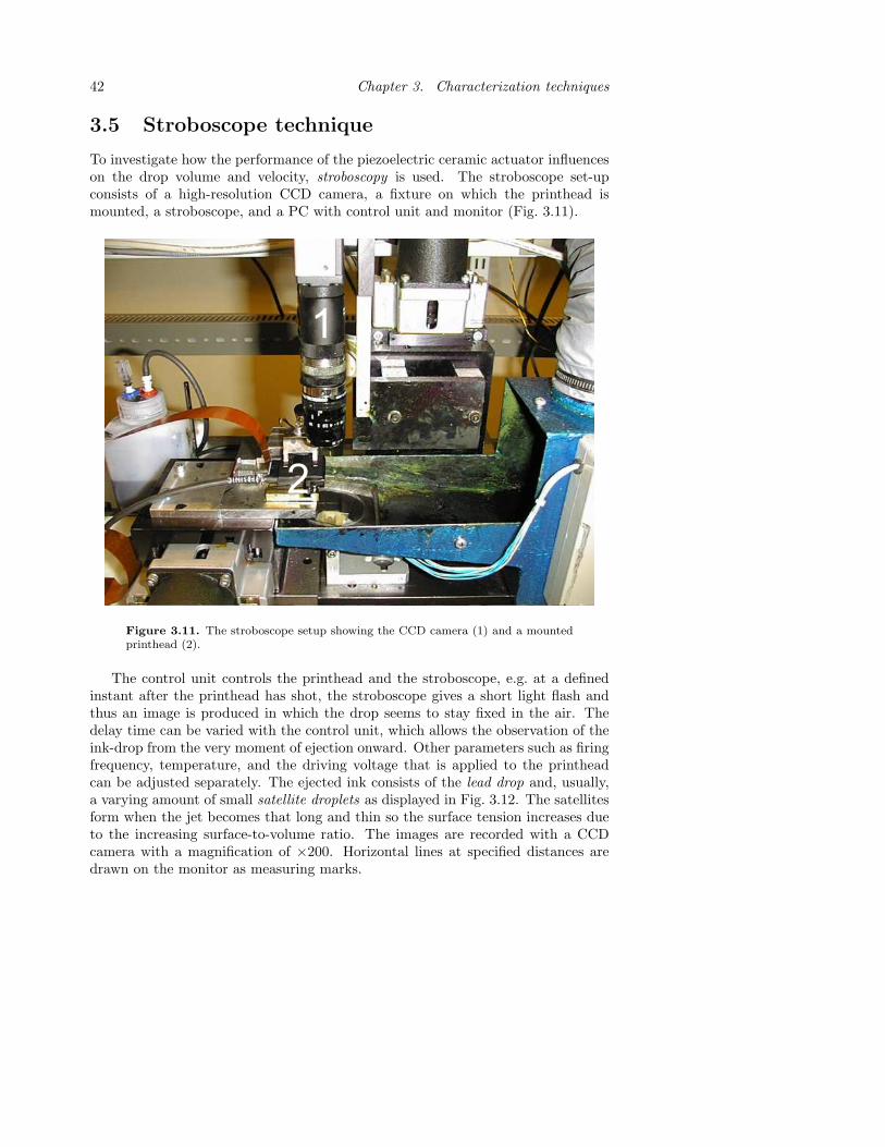
To investigate how the performance of the piezoelectric ceramic actuator influenceson the drop volume and velocity, stroboscopy is used. The stroboscope set-upconsists of a high-resolution CCD camera, a fixture on which the printhead ismounted, a stroboscope, and a PC with control unit and monitor (Fig. 3.11).
1
2
Figure 3.11. The stroboscope setup showing the CCD camera (1) and a mountedprinthead (2).
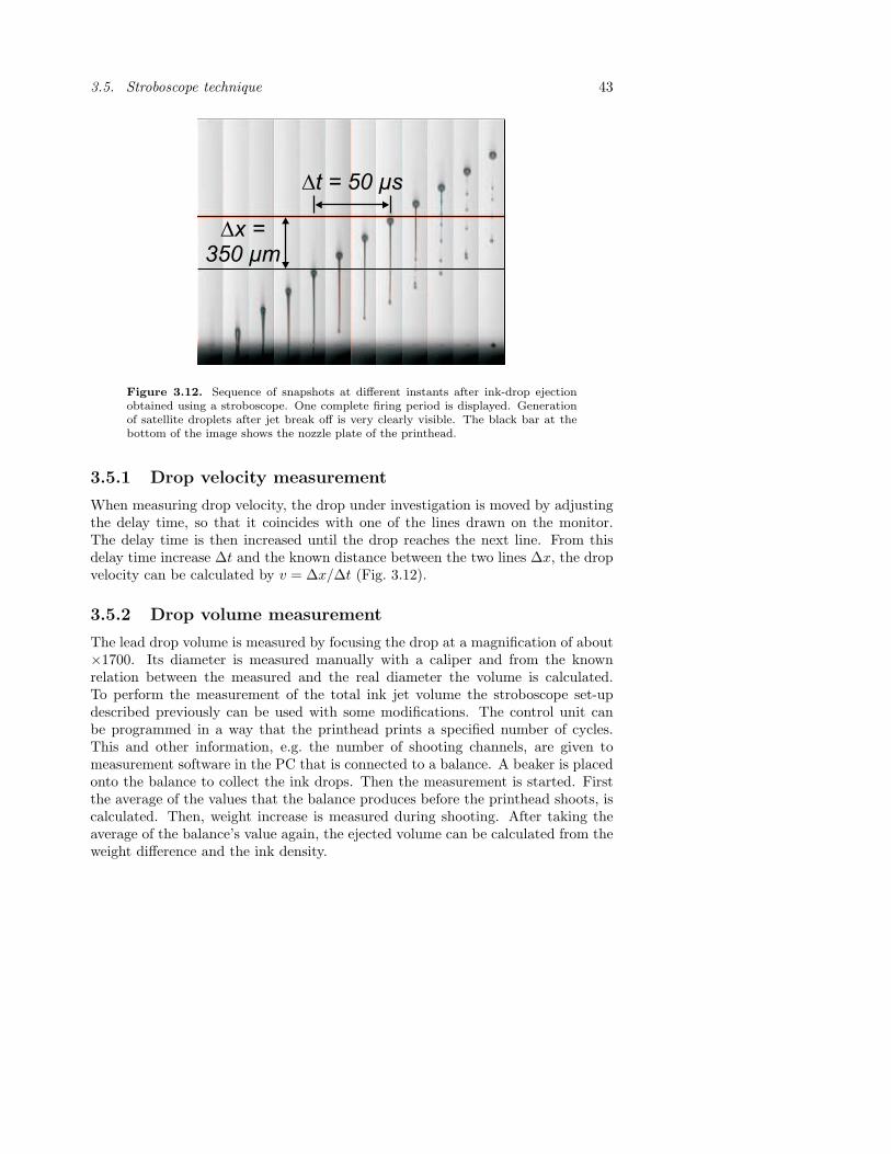
The control unit controls the printhead and the stroboscope, e.g. at a definedinstant after the printhead has shot, the stroboscope gives a short light flash andthus an image is produced in which the drop seems to stay fixed in the air. Thedelay time can be varied with the control unit, which allows the observation of theink-drop from the very moment of ejection onward. Other parameters such as firingfrequency, temperature, and the driving voltage that is applied to the printheadcan be adjusted separately. The ejected ink consists of the lead drop and, usually,a varying amount of small satellite droplets as displayed in Fig. 3.12. The satellitesform when the jet becomes that long and thin so the surface tension increases dueto the increasing surface-to-volume ratio. The images are recorded with a CCDcamera with a magnification of ×200. Horizontal lines at specified distances aredrawn on the monitor as measuring marks.
3.5. Stroboscope technique 43
Dx =350 µm
Dt = 50 µs
Figure 3.12. Sequence of snapshots at different instants after ink-drop ejectionobtained using a stroboscope. One complete firing period is displayed. Generationof satellite droplets after jet break off is very clearly visible. The black bar at thebottom of the image shows the nozzle plate of the printhead.
3.5.1 Drop velocity measurement
When measuring drop velocity, the drop under investigation is moved by adjustingthe delay time, so that it coincides with one of the lines drawn on the monitor.The delay time is then increased until the drop reaches the next line. From thisdelay time increase ∆t and the known distance between the two lines ∆x, the dropvelocity can be calculated by v = ∆x/∆t (Fig. 3.12).
3.5.2 Drop volume measurement
The lead drop volume is measured by focusing the drop at a magnification of about×1700. Its diameter is measured manually with a caliper and from the knownrelation between the measured and the real diameter the volume is calculated.To perform the measurement of the total ink jet volume the stroboscope set-updescribed previously can be used with some modifications. The control unit canbe programmed in a way that the printhead prints a specified number of cycles.This and other information, e.g. the number of shooting channels, are given tomeasurement software in the PC that is connected to a balance. A beaker is placedonto the balance to collect the ink drops. Then the measurement is started. Firstthe average of the values that the balance produces before the printhead shoots, iscalculated. Then, weight increase is measured during shooting. After taking theaverage of the balance’s value again, the ejected volume can be calculated from theweight difference and the ink density.

44

Part II
Our research
45

46
Chapter 4
Physical properties of Xaarinkjet actuators
During this analysis, the actuators were treated in different ways, such as ele-vated temperature and high voltage cycling. From this we obtained informationon material properties, e.g. the dielectric permittivity and the Curie Temperature.Furthermore, the influence of changes in the actuator geometry on the resonancebehavior was investigated.
Details and experimental results are given in Paper 1, Paper 2, Paper 4, andPaper 5.
4.1 Temperature dependence of the dielectricproperties
The temperature dependence of the channel wall capacitance (dielectric permittiv-ity) and dielectric loss factor (tan δ) was measured using the experimental setupsfor dielectric spectroscopy described in Chapter 3.1 and for pulsed spectroscopydescribed in Chapter 3.3. For the heat treatment the actuator was placed in anoven as described in the introduction of Chapter 3. Because of the sensitivity ofthe PZT material to any heat treatment, both measurements were performed si-multaneously within the same temperature cycle. The data from the Fluke 6304was recorded continuously over the whole temperature range, while the pulsed tech-nique was measured in 10 °C steps. Fig. 4.1 shows typical temperature dependenceof dielectric permittivity and loss tan δ for a channel wall.
To deduce the temperature dependence, measurements were made on virginchannel walls and for the same channel walls after the treatment. Applying theCurie-Weiss law (Eq. 2.5) to the reciprocal of the measured capacitance data gave
47

48 Chapter 4. Physical properties of Xaar inkjet actuators
300 325 350 375 400
3.5
4.0
4.5
5.0
5.5
6.0
6.5 RCL-MeterPulsed technique
Cap
acita
nce
C, n
F
Temperature T, K
5
6
7
8
Die
lect
ric lo
ss ta
nd, %
0.8
0.9
1.0
1.1
1.2
1.3
1.4
1.5
Die
lect
ricpe
rmitt
ivity
e',
103
Figure 4.1. Dielectric permittivity and loss factor as functions of temperaturemeasured with RCL-Meter and using pulsed technique.
the Curie temperature of the PZT material. The obtained number of TC = 508 Kwas comparable with the value given by the manufacturer of 498 K (see AppendixA).
Details on the temperature dependence of the PZT channel walls are given inPaper 1, Paper 2 and Paper 5.
4.2 Frequency dispersion
To measure frequency dispersion of dielectric permittivity and losses the dielectricspectroscopy setup, described in Chapter 3.1, and the pulsed spectroscopy setup,described in Chapter 3.3, were used. The Fluke 6304 RCL meter measures in a fre-quency range from 100 Hz to 100 kHz. Fig. 4.2 displays the dispersion of dielectricpermittivity and loss tan δ for a channel wall at 300 K and 380 K. To investigateat higher frequency ranges, from 1 kHz to 15 MHz, an HP4194A Impedance Ana-lyzer was used (Fig. 3.2). The most interesting frequency range is around 1 MHz,since within this range the main resonance frequency of the channel walls can befound. In Fig. 4.3, the dielectric permittivity of a virgin and a heat treated channelwall is plotted. Besides the main resonance, several subharmonics are clearly visible.
Detailed discussions on the obtained results are given in Paper 1, Paper 2 andPaper 5.

4.2. Frequency dispersion 49
0.1 1 10 1003
4
5
6
7
8
9
T = 380 K
300 K
Die
lect
ric lo
ss ta
nd
, %
Frequency f, kHz
3.5
4.0
4.5
5.0
5.5
6.0
0109-7611 10/11D
iele
ctric
per
mitt
ivity
e ¢, 1
03
Figure 4.2. Frequency dispersion of the dielectric permittivity and dielectric lossat 300 K and 380 K measured with Fluke 6304.
0.0 0.5 1.0 1.5 2.0
0.6
0.7
0.8
Frequency f, MHz
Cap
aci
tanc
eC
,nF
2.5
3.0
3.5
T = 300 K
0115-0755 10/11
f4
= 0.24 MHz
f2
= 1.27 MHz
f1
= 1.1 MHz
f3
= 0.58 MHz
Die
lect
ric
perm
itivi
tye
¢,10
3
Figure 4.3. Dispersion of dielectric permittivity measured with a HP4194A inthe frequency range from 1 kHz to 2 MHz. The resonance frequency and severalsubharmonics are clearly visible.

50 Chapter 4. Physical properties of Xaar inkjet actuators
4.3 Ferroelectric fatigue
Ferroelectric hysteresis loop tracing, as described in Chapter 3.4, gives informationon the polarization of the PZT material. High electric fields are needed to inducesaturation polarization of the channel walls. Cycling the electric field (triangularsignal of 88.5 kV/cm, 50 Hz) leads to a decrease in polarization. The decrease of theremnant polarization as function of the number of cycles is displayed in Fig. 4.4a.
Reason for this is the electrode arrangement in the actuator. In the Xaaractuator case the electric field is applied perpendicular to the polarization direction.Thus, during cycling the electric field, ‘weak’ dipols will rotate to be aligned in fielddirection.
Investigation of a virgin channel wall with a polarization microscope showeda homogeneous polarization over the whole top surface (’1’ in the right panel ofFig. 4.5). Channel wall ’2’ is a neighbouring wall experienced the high electricfield. After the treatment the polarization pattern of the element has changed.In polarised light clusters of grains along the PZT - Al interface appear brighterthan grains in the middle of the top surface. After grinding the top of the elementby approximately 20 µm the clusters disappeared and the top surface becomeshomogeneous like the virgin element. The electric field applied during the treatmentwas 88.5 kV/cm, so, high enough to polarize the element. Since the virgin elementwas already polarized in perpendicular field direction the high voltage treatmentinitialised a reorientation of the ferroelectric dipoles towards the direction of thefield. This is visible in polarised light as clusters. The investigated clusters appearedvery bright; therefore 90° rotation of the light is assumed which coincides with adipole reorientation of 90°. The reorientation starts at the PZT-Al interface at thetop surface of the element. At that position the grains were not clamped as muchas in the middle of the ceramic. Evidence for this is the non-changed area in themiddle of the top surface and that the grinded surface did not show any reorientedgrains at all.
Another observation was, that applying Eq. 4.1 to the array of P −E loops wesucceeded to envelop all loops into one major loop (the initial loop) as shown inFig. 4.4b.
Eeff = (E − 4πP × α)× β (4.1)
α, β and Pr as functions of the number of cycles are displayed in the insert to Fig.4b. The exact role of the coefficients α and β is still not clear to use and will befurther investigated.
More details on ferroelectric fatigue are given in Paper 2 and Paper 5.
4.3. Ferroelectric fatigue 51
-100 -50 0 50 100
-40
-20
0
20
40
b)
Effective electric field Eeff
, kV/cm
-40
-20
0
20
40
-100 -50 0 50 100
a)
Electric field E, kV/cm
Eeff
= [ E - 4pP ´ a ] ´ b
Pol
ariz
atio
nP
,mC
/cm
2
0 30 60 900.0
0.5
1.0 a
b
a, b
Number of cycles, 103
25.0
27.5
30.0
Pr
Pr,
mC
/cm
2
Figure 4.4. a) A series of ferroelectric hysteresis loops obtained with a modifiedSawyer-Tower circuit. With increasing number of cycles (1 to 90,000) the remnantpolarization decreases and the coercive field increases. b) Applying Eq. 4.1, all loopsenvelop into one major loop. Insert: α, β and Pr as functions of the number ofcycles

52 Chapter 4. Physical properties of Xaar inkjet actuators
j
j
k
k
Electrodes Fatigued PZT
Figure 4.5. Left panel: SEM micrograph (×300) of an array of micromachinedchannel walls. Right panel: Optical microscope image taken in polarized light show-ing a virgin element ’1’ and an element ’2’ treated by a triangular signal of E =88.5 kV/cm at 50 Hz. The treated wall shows clearly a fatigued area close to theelectrodes on both sides.

4.4. Acoustic resonance modes 53
4.4 Acoustic resonance modes
Two different approaches were made to investigate resonance modes of the actuator.The first one, the manual resonance test, uses an HP4194A Impedance Analyzershown in the dielectric spectroscopy set-up (Chapter 3.1) and is explained in detailin Chapter 3.2. The other method is based on the pulsed spectroscopy which isdescribed in Chapter 3.3.
As shown in Fig. 4.3, there are several additional subharmonics beside the mainresonance at 1.1 MHz. To clarify the nature of these resonance modes, a spectro-scopic study on a specially made actuator was made. The actuator was diagonallycut to get an array of 128 channel walls of different lengths: from 4.3 to 10 mm(Fig. 4.6. The ‘short’ channels walls have a variable height and a non-clamped top.The ‘long’ channels have 360 µm high channels walls clamped on bottom and top.The resonance characteristics of the 128 channels is given in Fig. 4.7.
Figure 4.6. Specially made actuator with ‘short’ (4.3 mm) and ‘long’ (10 mm)channels.
As clearly seen, there are eight weak low-frequency resonance peaks whose po-sitions do not depend on the channel wall length, whereas there are two resonancesat frequencies between 1.0 and 1.2 MHz which change their amplitude and positionat different channel lengths. With channel elongation these two resonances comecloser, merge together and form a single strong resonance peak at 1.1 MHz.
To get an idea on the parameters which control the acoustic spectra and ona frequency scale, one can consider the vibrations of the walls as oscillations of aslender beam with different boundary conditions at the edges. Resonance frequencyof different modes ηi,n can be found in [31]:
fi,n =12π
d
h2
√E
12(1− ν2)ρη2
i,n , (4.2)
where index i stands for the acoustic mode type, while n is the mode number, dis the thickness and h is the height of the channel wall, E is the elastic modulus,ν is the Poisson ratio and ρ is the mass density. Bottom clamped channel wallsoscillate as cantilevers and the first two modes are:
ηI,1 = 1.875, ηI,2 = 4.694.
54 Chapter 4. Physical properties of Xaar inkjet actuators
0.2 0.4 0.6 0.8 1.0 1.2 1.4
0.4
0.5
0.6
0.7
10
4.3
Chann
el le
ngth
l, m
mC
apac
itanc
eC
, nF
Frequency f, MHz
Figure 4.7. Capacitance-frequency (C−f) characteristics of an array of 128 channelwalls of different length (4.3 to 10 mm).
The fundamental mode of both, bottom- and top-clamped walls is:
ηII,1 = 4.730.
Although the Eq. 4.2 gives a very crude approximation to the real channel wallspectra, they describe the main observations in Fig. 4.7. We believe that the firsteight features are the cantilever-type. They come from the shallow part of channelswith non-clamped tops. This part of the channel walls is similar in both, ‘short’and ‘long’ channels thus the resonance frequencies are the same for the whole array.Eq. 4.2 does not give all the resonance modes since the channel walls have variableheight, however it shows the correct order of the resonance frequencies as well asdependence on the thickness d and thickness-to-height d/h aspect ratio. The nexttwo resonance features between 1 and 1.2 MHz in the ‘short’ channels we identifyas fI,2 and fII,1 resonance modes. They are very close since fII,1/fI,2 = 1.015,and with channels elongation/deepening the frequency fII,1 ∝ 1/h2 decreases andmerges to fI,2.
The resonance spectra are complicated due to spurious oscillations and, as fin-gerprints, vary between actuators. Many issues should be accounted to make quan-titative spectra analyses: variable channel depth, different compliance of the sup-ports at the built-in and top-glued ends of the channel walls, the effects of sawingdamage, effects of electrical polarization, etc.
Observations made with the pulsed spectroscopic technique are given and dis-cussed in Chapter 3.3 and in Paper 1, Paper 2, Paper 4, and Paper 5.
4.5. Correlation with inkjet performance 55
4.5 Correlation with inkjet performance
The setup given in Chapter 3.5 is used to correlate properties of the channel wallsto the performance of the printhead. The influence of high voltage and tempera-ture treatments could be revealed in this way as shown in Fig. 4.8. If possible, onlypart of the whole channel wall array was treated to keep the non-treated part asreference.
Experimental results are given in Paper 4 and Paper 5.
6.0
6.5
7.0
a)
T = 300 K
Dro
pve
loci
ty,m
/s
25
30
35
40
Lea
ddro
pvo
lum
e,pl
20 30 40 50 60 706.0
6.5
7.0
b)
Channel number
25
30
35
40
Figure 4.8. Degradation of drop velocity and lead drop volume due to a) highvoltage treatment, b) temperature treatment.

56
Chapter 5
Thermometry inside inkjetactuators
The possibility is investigated to use the capacitance of the channel walls as atemperature sensor. This chapter describes equipment made to measure the ca-pacitance of the channel walls and describes some measurements that were madeto check the functionality of the equipment and to investigate the magnitude oftemperature changes inside the actuator.
I started the research on this topic already in April 1999 as subject of myMaster’s Thesis [33]. The research was continued and refined in the beginning of myPh.D. studies. Onne Wouters from the University of Groningen, The Netherlandsand Andreas Jorzick, XaarJet AB, joined the research partly in 1999 respectively2001.
The results are published in Paper 3, in WO Patent no. 02/26500, and [34].
5.1 Introduction
Temperature compensation is necessary to enable a constant drop velocity through-out the whole temperature range of the operating printhead (10 °C - 60 °C). Thedrop velocity depends on the viscosity of the printed fluid. As the viscosity ofthe fluid has a temperature dependency, the velocity of the ejected droplets is alsotemperature dependent. Regulation of the temperature inside the printhead tocontrol the viscosity of the fluid and therefore the drop speed is not possible. Butit is possible to control the driver voltage of the printhead. This driver voltage isresponsible for the movement of the channel walls.
In the standard XaarJet printhead, a thermistor is used to regulate indextem-perature!regulation the driver voltage depending on the temperature close to theactuator. Investigations of the temperature distribution inside the printhead haveproved that the temperature measurement with the thermistor is not sufficient for
57

58 Chapter 5. Thermometry inside inkjet actuators
a fast and precise regulation of the drop velocity [33]. The goal was to improve thetemperature compensation by using the walls between the dummy channels as tem-perature sensitive elements inside the actuator (Fig. 5.2). The linear temperaturebehavior of the capacitance of the dummy channel walls in the operating temper-ature range was demonstrated in experiments (Fig. 5.1). With this knowledge, anew temperature compensation circuit based on a voltage divider as a metrologytechnique was built up. Finally, experiments proved that the temperature compen-sation circuit works in a proper manner and gives the expected results for lineartemperature compensation.
5.2 Theoretical background
5.2.1 Temperature compensation
During printing the temperature inside the printhead changes. The major heatsources are the driver chips, the actuator and the electrical components of the PCB(printed circuit board). To remove most of the heat, the chips and the PCB areglued onto an aluminium base plate. The base plate temperature can be controlledby an external cooling system. The amount of heat produced depends on thefiring frequency and the number of firing channels. If the printhead is firing 100%,most heat will be generated. During normal printing the firing frequency and thenumber of firing channels are changing and therefore the temperature inside theprinthead, especially inside the actuator, fluctuates. Temperature fluctuations ofthe actuator also causes fluctuations of the ink temperature. The ink viscosityshows a temperature dependency, which can be explained by the strength of theatomic bonding between the ink molecules. At higher temperatures the oscillationof the ink molecules is lager and the strength of the atomic bonding is reduced.The viscosity of a typical oil-based ink for example decreases from 11 to 8 mPa·swith temperature increase from 30 to 40 °C. Less of the force, exerted onto the inkdue to the deflection of the channel walls is necessary to break the atomic bondingof the ink molecules. Therefore more of the force will be transformed into thevelocity of the ink drops. If not compensated the viscosity variations would leadto significant changes in drop velocity and volume, 9% and 13%, respectively, asmeasured with Xaar-type actuators [20]. A regulation of drop velocity and volumecan by performed by matching the driver voltage to the temperature inside theprinthead.
5.2.2 Existing temperature compensation
In the standard XaarJet printhead the temperature compensation is achieved byregulating the driving voltage (V 100) with a thermistor (Rtherm). This thermistor
5.2. Theoretical background 59
is placed close to the actuator (Fig. 5.3). The electrical behavior of Rtherm as afunction of temperature T is given from the manufacturer as:
Rtherm = 105 · e3700[1/(T+273.15)−1/298.5] (5.1)
Rtherm is part of the temperature compensation circuit, which is implemented onthe PCB together with the driver chip. This circuit generates and regulates theV 100 signal.
V 100 = V(chip) ·R7 · (1 + Rtherm/R2)/(R8 + R7) , (5.2)
where R2, R7 and R8 are as well parts of the compensation circuit. V(chip) isadjusted for each printhead to make all printheads have the same average dropvelocity.
If the temperature of the actuator increases the temperature of the thermistoralso increases and Rtherm will decrease (Eq. 5.1). V 100, which is proportional toRtherm, will therefore also decrease. A decrease of V 100 lowers the wall motionand the drop speed is reduced. In this way drop speed as a function of the actuatortemperature is kept constant.
The big draw back with this kind of temperature compensation is the high timeconstant of the sensing element.
5.2.3 Temperature dependence of channel wall capacitance
A channel wall covered with electrodes can be viewed as a common plate capacitorwhose capacitance is given by:
C =ε ·A
d(5.3)
where ε is the dielectric constant of the PZT material, A the electrode surface areaand d the thickness of the wall.
Writing x · y for A and differentiating with respect to temperature gives:
∂C
∂T=
xy
d
∂ε
∂T+
εy
d
∂x
∂T+
εx
d
∂y
∂T− εxy
d2
∂d
∂T(5.4)
⇒ 1C
∂C
∂T=
1ε
∂ε
∂T+
1x
∂x
∂T+
1y
∂y
∂T− 1
d
∂d
∂T(5.5)
Assuming an isotropic linear thermal expansion coefficient αl this equation reducesto:
1C
∂C
∂T=
1ε
∂ε
∂T+ αl (5.6)
Fig. 5.1 shows the capacitance of channel walls for different temperatures.
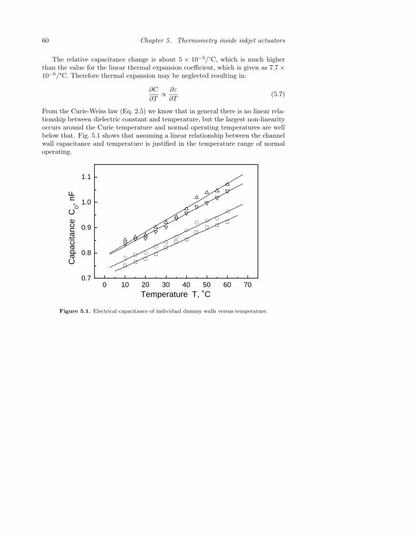
60 Chapter 5. Thermometry inside inkjet actuators
The relative capacitance change is about 5 × 10⁻³/°C, which is much higherthan the value for the linear thermal expansion coefficient, which is given as 7.7×10⁻⁶/°C. Therefore thermal expansion may be neglected resulting in:
∂C
∂T∝ ∂ε
∂T(5.7)
From the Curie-Weiss law (Eq. 2.5) we know that in general there is no linear rela-tionship between dielectric constant and temperature, but the largest non-linearityoccurs around the Curie temperature and normal operating temperatures are wellbelow that. Fig. 5.1 shows that assuming a linear relationship between the channelwall capacitance and temperature is justified in the temperature range of normaloperating.
0 10 20 30 40 50 60 70 0.7
0.8
0.9
1.0
1.1
Cap
acita
nce
C D
, nF
Temperature T , ˚C
Figure 5.1. Electrical capacitance of individual dummy walls versus temperature.

5.3. Experimental setup 61
5.3 Experimental setup
5.3.1 Modification of the printhead
In every actuator four extra channels are sawn, two on each side. These channelsare not used for drop generation but are made to give the first real firing channelthe same characteristics as the channels in, for instance, the centre of the actua-tor. These so called ‘dummy channels’ are used in the temperature measurements(Fig. 5.2).
Dummy Channels
Dummy Wall
Active Channels
Figure 5.2. Actuator cross section and ’dummy wall’
It is not possible to solder a wire manually onto the bond pad on the back sideof the actuator. Instead, two bigger bond pads have to be placed somewhere nearthe actuator (Fig. 5.3). Using a wire bond these larger pads were connected withthe pads on the actuator and larger wires can be soldered to the bigger pads andtaken out off the printhead.
Chip
Thermistor
AdditionalWirebond
Connection
Actuator(with filter)
Figure 5.3. Image showing the position of Rtherm and the additional wirebondconnections for electrical connection of the dummy walls
5.3.2 Electronics
A voltage divider circuit, shown in Fig. 5.4, was chosen to monitor the capacitanceCD of a dummy wall. The dummy wall was connected in series with an external,
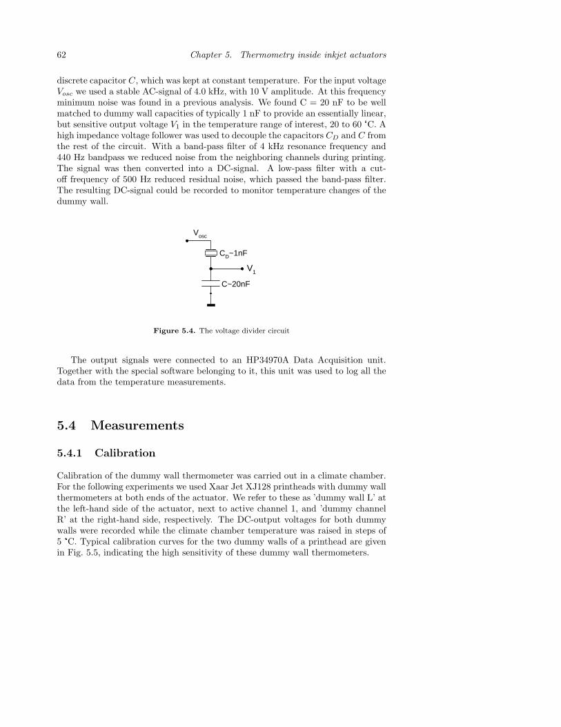
62 Chapter 5. Thermometry inside inkjet actuators
discrete capacitor C, which was kept at constant temperature. For the input voltageVosc we used a stable AC-signal of 4.0 kHz, with 10 V amplitude. At this frequencyminimum noise was found in a previous analysis. We found C = 20 nF to be wellmatched to dummy wall capacities of typically 1 nF to provide an essentially linear,but sensitive output voltage V1 in the temperature range of interest, 20 to 60 °C. Ahigh impedance voltage follower was used to decouple the capacitors CD and C fromthe rest of the circuit. With a band-pass filter of 4 kHz resonance frequency and440 Hz bandpass we reduced noise from the neighboring channels during printing.The signal was then converted into a DC-signal. A low-pass filter with a cut-off frequency of 500 Hz reduced residual noise, which passed the band-pass filter.The resulting DC-signal could be recorded to monitor temperature changes of thedummy wall.
V osc
C D ~1nF
C ~20nF
V 1
Figure 5.4. The voltage divider circuit
The output signals were connected to an HP34970A Data Acquisition unit.Together with the special software belonging to it, this unit was used to log all thedata from the temperature measurements.
5.4 Measurements
5.4.1 Calibration
Calibration of the dummy wall thermometer was carried out in a climate chamber.For the following experiments we used Xaar Jet XJ128 printheads with dummy wallthermometers at both ends of the actuator. We refer to these as ’dummy wall L’ atthe left-hand side of the actuator, next to active channel 1, and ’dummy channelR’ at the right-hand side, respectively. The DC-output voltages for both dummywalls were recorded while the climate chamber temperature was raised in steps of5 °C. Typical calibration curves for the two dummy walls of a printhead are givenin Fig. 5.5, indicating the high sensitivity of these dummy wall thermometers.
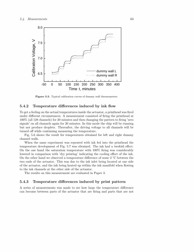
5.4. Measurements 63
-50 0 50 100 150 200 250 300 350 400
6.5
7.0
7.5
8.0
dummy wall L dummy wall R
Cal
ibra
tion
Vol
tage
, V
Time t , minutes
Figure 5.5. Typical calibration curves of dummy wall thermometers.
5.4.2 Temperature differences induced by ink flow
To get a feeling on the actual temperatures inside the actuator, a printhead was firedunder different circumstances. A measurement consisted of firing the printhead at100% (all 128 channels) for 20 minutes and then changing the pattern to firing ’zerosignals’ on all channels again for 20 minutes. In this mode the chip will be runningbut not produce droplets. Thereafter, the driving voltage to all channels will beturned off while continuing measuring the temperature.
Fig. 5.6 shows the result for temperatures obtained for left and right dummychannel walls.
When the same experiment was repeated with ink fed into the printhead thetemperature development of Fig. 5.7 was obtained. The ink had a twofold effect.On the one hand the saturation temperature with 100% firing was considerablylowered in comparison with ’dry printing’ indicating the cooling effect of the ink.On the other hand we observed a temperature difference of some 2 °C between thetwo ends of the actuator. This was due to the ink inlet being located at one sideof the actuator, and the ink being heated up within the ink manifold when flowingto the ink channels at the other side of the actuator.
The results on this measurement are evaluated in Paper 3.
5.4.3 Temperature differences induced by print pattern
A series of measurements was made to see how large the temperature differencecan become between parts of the actuator that are firing and parts that are not

64 Chapter 5. Thermometry inside inkjet actuators
0 10 20 30 40 50 60 20
30
40
50
60 dummy wall L dummy wall R
no firing zero firing 100% firing
Tem
pera
ture
T , ˚
C
Time t , minutes
Figure 5.6. Temperatures at both ends of the actuator when printing without ink
0 10 20 30 40 50 60 20
25
30
35
40 dummy wall L (ink inlet) dummy wall R
no firing zero firing 100% firing
Tem
pera
ture
T , ˚
C
Time t , minutes
Figure 5.7. Temperatures at both ends of the actuator when printing with ink
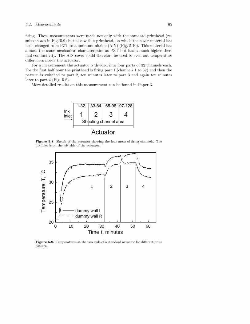
5.4. Measurements 65
firing. These measurements were made not only with the standard printhead (re-sults shown in Fig. 5.9) but also with a printhead, on which the cover material hasbeen changed from PZT to aluminium nitride (AlN) (Fig. 5.10). This material hasalmost the same mechanical characteristics as PZT but has a much higher ther-mal conductivity. The AlN-cover could therefore be used to even out temperaturedifferences inside the actuator.
For a measurement the actuator is divided into four parts of 32 channels each.For the first half hour the printhead is firing part 1 (channels 1 to 32) and then thepattern is switched to part 2, ten minutes later to part 3 and again ten minuteslater to part 4 (Fig. 5.8).
More detailed results on this measurement can be found in Paper 3.
1-32 33-64 65-96 97-128
Inkinlet
Actuator
Shooting channel area
1 2 3 4
Figure 5.8. Sketch of the actuator showing the four areas of firing channels. Theink inlet is on the left side of the actuator.
0 10 20 30 40 50 60 20
25
30
35
dummy wall L dummy wall R
4 3 2 1
Tem
pera
ture
T , ˚
C
Time t , minutes
Figure 5.9. Temperatures at the two ends of a standard actuator for different printpattern.

66 Chapter 5. Thermometry inside inkjet actuators
0 10 20 30 40 50 60 20
25
30
35
40 4 3 2 1
Tem
pera
ture
T , ˚
C
Time t , minutes
28 30 34.5
35.0
35.5
58 60
35.0
35.5
Figure 5.10. Temperature equilibration by usage of high thermally conductingmaterial (AlN) as cover.
5.5. Conclusions 67
5.5 Conclusions
The results of the calibration again show the linear relation between the ca-pacitance of the channel walls and their temperature. The large differencesbetween calibration results of different printheads, makes it necessary to cal-ibrate every printhead before measurements are made.
Fig. 5.6 shows that the output voltage follows temperature changes veryrapidly and the fact that the calculated temperatures for the two signals inFig. 5.6 stay exactly the same, indicate that the calibration is very accurately.
When the printhead is printing ink, the temperature decreases significantlyas shown in Fig. 5.7. The cooling effect of the ink flow is large.
Fig. 5.9 shows that in a normal printhead clear temperature differences canoccur if a very asymmetric pattern is fired for a long time. It is strange thatthe temperature measured on the right side of the printhead is higher whenfiring pattern 2 than it is firing pattern 1. A measurement of the current goinginto the printhead shows that the total power consumption of the printheadis lager when patterns 2 and 3 are fired. This can be caused by an largeraverage capacitance on the centre channels in the actuator.
These differences almost completely disappear when a cover of aluminumnitride is used (Fig. 5.10). It seems that using this cover is a good way toinsure equalization of the temperatures over all the channels.

68
Chapter 6
Chevron-type inkjet actuator
From the beginning of the Xaar shear mode concept, the idea of making a Chevrontype actuator existed. The Chevron actuator would use the whole channel wall asactive part instead using just the upper half as the standard actuator. This wouldmake the printhead much more powerful and should lead to less power consumptionand therefore less heat dissipation.
Onne Wouters from the University of Groningen, The Netherlands, ThomasJager [35] from Albert-Ludwigs-University of Freiburg, Germany and Gerald Richterfrom Chemnitz Technical University, Germany, joined the research partly in 1999,2002 and 2003, respectively.
The results were published in Paper 6 and are submitted to the European Meet-ing on Ferroelectrics EMF 2003, Cambridge, UK.
6.1 Introduction
The standard Xaar actuator consists of a non-polarized cover plate with the inkinlets and a polarized base plate with walls and channels. All the walls of a channelwafer are completely polarized in one direction. To be able to bend the wall properlyonly a part of the wall should be active. Therefore the upper part of each wall isplated with aluminium electrodes. From calculations and experiments an electrodedepth of 43% is found to be the optimum for drop ejection.
To improve Xaar actuators in respect of print performance and power consump-tion, Chevron design is proposed. Figs. 6.1 show in simplified cross section sketchesthe main constituents of (a) a standard XJ128 actuator and (b) an actuator ofChevron design. As displayed, the Chevron actuator includes an additional PZTlayer with polarization in opposite direction of the base plate polarization. Fur-thermore, the depth of the aluminium electrodes is increased, thus they cover thechannel walls completely from top (where the cover plate is attached) to bottom ofthe channel.
69
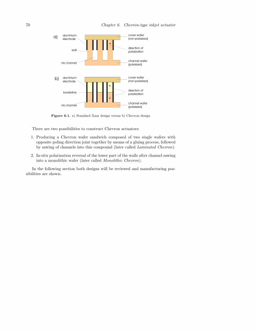
70 Chapter 6. Chevron-type inkjet actuator
a)
b)
wall
ink channel
aluminium
electrode
direction of
polarization
cover wafer
(non-polarized)
channel wafer
(polarized)
borderline
ink channel
aluminium
electrode
direction of
polarization
cover wafer
(non-polarized)
channel wafer
(polarized)
Figure 6.1. a) Standard Xaar design versus b) Chevron design
There are two possibilities to construct Chevron actuators:
1. Producing a Chevron wafer sandwich composed of two single wafers withopposite poling direction joint together by means of a gluing process, followedby sawing of channels into this compound (later called Laminated Chevron).
2. In-situ polarization reversal of the lower part of the walls after channel sawinginto a monolithic wafer (later called Monolithic Chevron).
In the following section both designs will be reviewed and manufacturing pos-sibilities are shown.
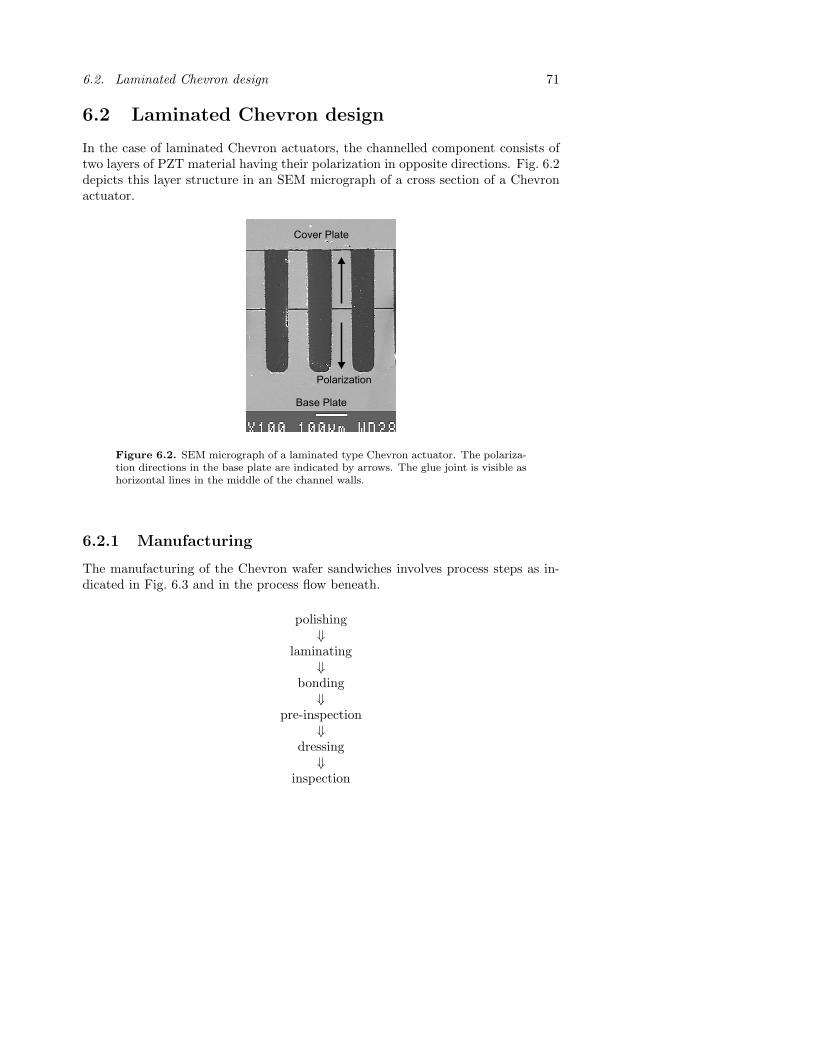
6.2. Laminated Chevron design 71
6.2 Laminated Chevron design
In the case of laminated Chevron actuators, the channelled component consists oftwo layers of PZT material having their polarization in opposite directions. Fig. 6.2depicts this layer structure in an SEM micrograph of a cross section of a Chevronactuator.
Cover Plate
Base Plate
Polarization
Figure 6.2. SEM micrograph of a laminated type Chevron actuator. The polariza-tion directions in the base plate are indicated by arrows. The glue joint is visible ashorizontal lines in the middle of the channel walls.
6.2.1 Manufacturing
The manufacturing of the Chevron wafer sandwiches involves process steps as in-dicated in Fig. 6.3 and in the process flow beneath.
polishing⇓
laminating⇓
bonding⇓
pre-inspection⇓
dressing⇓
inspection
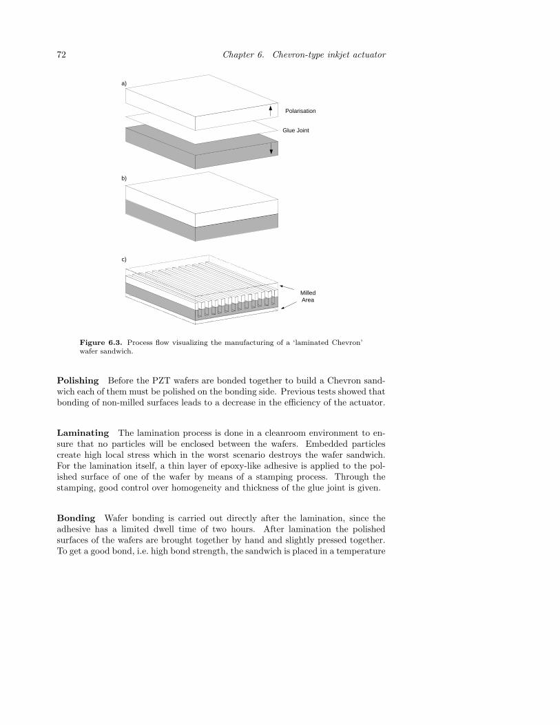
72 Chapter 6. Chevron-type inkjet actuator
Glue Joint
Polarisation
Milled Area
a)
b)
c)
Figure 6.3. Process flow visualizing the manufacturing of a ‘laminated Chevron’wafer sandwich.
Polishing Before the PZT wafers are bonded together to build a Chevron sand-wich each of them must be polished on the bonding side. Previous tests showed thatbonding of non-milled surfaces leads to a decrease in the efficiency of the actuator.
Laminating The lamination process is done in a cleanroom environment to en-sure that no particles will be enclosed between the wafers. Embedded particlescreate high local stress which in the worst scenario destroys the wafer sandwich.For the lamination itself, a thin layer of epoxy-like adhesive is applied to the pol-ished surface of one of the wafer by means of a stamping process. Through thestamping, good control over homogeneity and thickness of the glue joint is given.
Bonding Wafer bonding is carried out directly after the lamination, since theadhesive has a limited dwell time of two hours. After lamination the polishedsurfaces of the wafers are brought together by hand and slightly pressed together.To get a good bond, i.e. high bond strength, the sandwich is placed in a temperature
6.2. Laminated Chevron design 73
controlled pneumatic press. There, a constant temperature of 100 °C and a pressureof 2 bar is applied for 15 minutes to the wafers.
Pre-inspection After bonding, the wafer sandwiches are inspected for damages,i.e. cracks or broken edges. Also sandwiches with a wafer-to-wafer misalignmentare rejected.
Dressing Since the as-bonded wafer sandwiches have the thickness of two wafersthey have to be dressed to the proper size of 900 µm, which is the thickness of astandard wafer. A well defined amount of the PZT material has to be removed in amilling process from both sides of the sandwich. The ratio between top and bottomdepends on the actuator type (200 dpi or 360 dpi). E.g., for a 200 dpi Chevronactuator the upper PZT layer has a thickness of 200 µm whereas the bottom layeris 700 µm. Fig. 6.3c illustrates this process step.
Inspection To reveal enclosed air pockets, particles or cracks, the sandwichesare inspected by shining a very bright light source through from the backside.Embedded features appear as dark spots whereas areas of good bonds are bright.Unfortunately, this techniques doesn’t tell anything about the glue thickness andthe homogeneity of the adhesive layer.
In addition to PZT-PZT sandwiches, PZT-glass sandwiches were produced.This was done mainly to get an idea on the amount and size distribution of embed-ded air pockets. Due to the transparency of the glass wafers the glue joint couldbe investigated with an optical microscope.
6.2.2 Optimization of active layer thicknesses
The ratio between top and bottom PZT layer in the Chevron sandwich is veryimportant to achieve highly effective actuators. To find this ratio a number ofsimulations were performed using a Xaar internal software package specially de-veloped for Xaar -type actuators. The output of the software is drop velocity anddrop volume as functions of actuator geometry, driving voltage waveform and inkproperties. Fig. 6.4 shows the simulation results for an XJ-128 Chevron actuatorusing standard wall geometry (including two PZT layers), waveform and ink. Theoptimal height of the top PZT layer is found to be between 45% and 50% of thetotal height.
To confirm this data a set of special actuators was made. During manufacturingthe Chevron sandwich was slanted and in this way walls with top PZT layer rangingfrom 30% to 70% of the total height were achieved (Fig. 6.5).
The preparation of the slanted Chevron wafer is done in 3 steps.
1. Bonding of two standard PZT (900 µm height) wafers with polished surfacesin opposite polarization direction (Fig.6.6a);

74 Chapter 6. Chevron-type inkjet actuator
20 30 40 50 60 70 800
1
2
3
4
5
6
7
8
9
10
Dro
p ve
loci
ty, m
/s
Upper part of the Chevron wall (% of total height)
0
10
20
30
40
50
60
70
80
Dro
p vo
lum
e , p
L
Figure 6.4. Simulation results for a slanted actuator having different ratio betweenthe top and bottom half of the PZT sandwich. Optimal performance is expectedwhen the top PZT layer is 45% to 50% of the complete wall height.
.....
border
line
Figure 6.5. Arrangement of a slanted Chevron actuator to determine the best ratiobetween top and bottom PZT layer in the wafer sandwich.
2. Milling the wafer sandwich on a slanted chuck (wedge). The top wafer shouldhave a residual height from 111 µm to 259 µm (Fig. 6.6b) (correspond 30%to 70% of the whole wall height);
3. Turning around the wafer sandwich and milling it to a thickness of 900 µm(standard channel wafer size) (Fig.6.6c and Fig. 6.6d);
Fig.6.6 displays in brief the manufacturing of the slanted Chevron.The slanted Chevron sandwich was processed into actuators which were then
characterized using an HP4194A Impedance Analyzer. Fig. 6.7 gives the measuredadmittance data. The obtained results agree very well with the simulation shownin Fig. 6.4. The optimal top/bottom ratio was identified to be between 45/55 to50/50.

6.2. Laminated Chevron design 75
milled aera
milled aera
a)
b)
c)
wedge
d)
polarization
Figure 6.6. Production steps for making a slanted Chevron sandwich to determinethe best top to bottom ratio of the laminated PZT layers.
0 50 100 150 200 250 300 350 400 450 0.0025
0.0030
0.0035
0.0040
0.0045
0.0050
0.0055
0.0060
0.0065
0.0070
0.0075
uppe
r pa
rt o
f the
wal
l (%
of m
ax h
eigh
t)
Channel # (1-130 actuator#17; 156-280 actuator#11; 307-434 actuator#5)
delta
I (S
)
25
30
35
40
45
50
55
60
65
70 chevron borderline
Figure 6.7. Measurement data for the slanted Chevron confirming the numbersobtained by simulations (see Fig. 6.5).
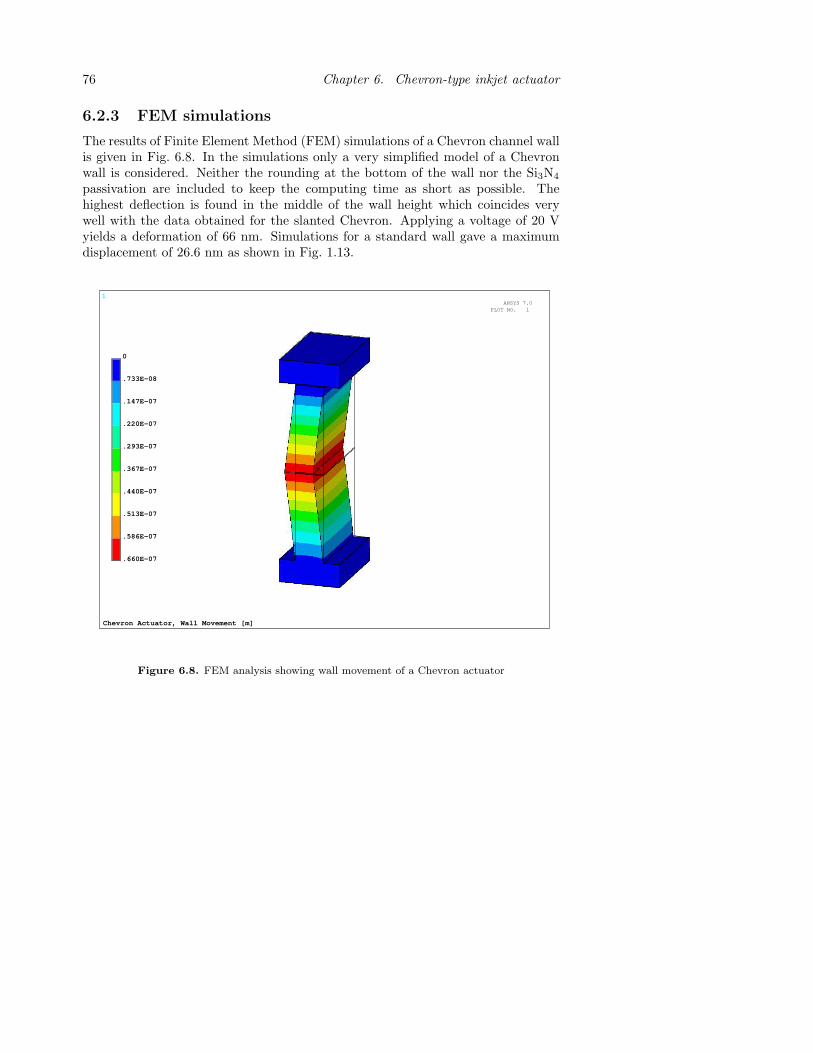
76 Chapter 6. Chevron-type inkjet actuator
6.2.3 FEM simulations
The results of Finite Element Method (FEM) simulations of a Chevron channel wallis given in Fig. 6.8. In the simulations only a very simplified model of a Chevronwall is considered. Neither the rounding at the bottom of the wall nor the Si3N4
passivation are included to keep the computing time as short as possible. Thehighest deflection is found in the middle of the wall height which coincides verywell with the data obtained for the slanted Chevron. Applying a voltage of 20 Vyields a deformation of 66 nm. Simulations for a standard wall gave a maximumdisplacement of 26.6 nm as shown in Fig. 1.13.
1
Chevron Actuator, Wall Movement [m]
0
.733E-08
.147E-07
.220E-07
.293E-07
.367E-07
.440E-07
.513E-07
.586E-07
.660E-07
ANSYS 7.0PLOT NO. 1
Figure 6.8. FEM analysis showing wall movement of a Chevron actuator

6.2. Laminated Chevron design 77
6.2.4 Influence of glue joint thickness
A series of experiments have been carried out to investigate the influence of theglue joint thickness on the performance of the Chevron actuator. It was found thatthicker glue joints result in a change of resonance frequency of the channel wall.As long the joint has an equal thickness over the whole actuator the impact on theprint performance is negligible. Only variations within the actuator can be seenas inhomogeneities in drop velocity. Fig. 6.9 shows an example for a 500 channelsChevron actuator with glue joint variations of up to 5 µm.
0 100 200 300 400 500 5.0
5.5
6.0
6.5
Dro
p ve
loci
ty, m
/s
Channel number
Figure 6.9. Drop velocity variation caused by non-uniform glue joint thickness
6.2.5 Alternative bonding method
An alternative way of preparing the Chevron sandwich is to use a so called BondAligner as known in the semiconductor industry (e.g. SB6 from Karl Suess). Thisprocess comprises good temperature control, well defined mechanical pressure forthe bonding and, most important, the bonding can be performed in vacuum at-mosphere. This could be a key element in making Chevron sandwiches withoutembedded air pockets. Until now only pre-studies have been carried out on thistopic. Here, I would like to thank Prof. Stemme and Frank Niklaus from theS3/MST Department at KTH for their generous help and assistance.
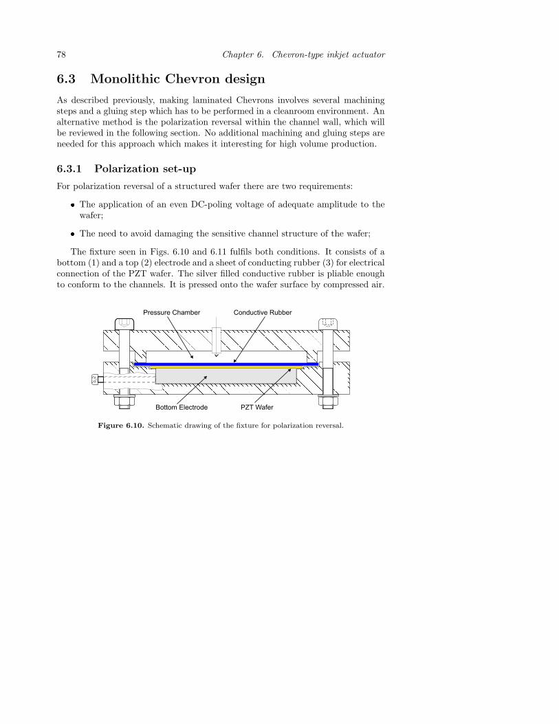
78 Chapter 6. Chevron-type inkjet actuator
6.3 Monolithic Chevron design
As described previously, making laminated Chevrons involves several machiningsteps and a gluing step which has to be performed in a cleanroom environment. Analternative method is the polarization reversal within the channel wall, which willbe reviewed in the following section. No additional machining and gluing steps areneeded for this approach which makes it interesting for high volume production.
6.3.1 Polarization set-up
For polarization reversal of a structured wafer there are two requirements:
The application of an even DC-poling voltage of adequate amplitude to thewafer;
The need to avoid damaging the sensitive channel structure of the wafer;
The fixture seen in Figs. 6.10 and 6.11 fulfils both conditions. It consists of abottom (1) and a top (2) electrode and a sheet of conducting rubber (3) for electricalconnection of the PZT wafer. The silver filled conductive rubber is pliable enoughto conform to the channels. It is pressed onto the wafer surface by compressed air.
Bottom Electrode
Pressure Chamber Conductive Rubber
PZT Wafer
Figure 6.10. Schematic drawing of the fixture for polarization reversal.
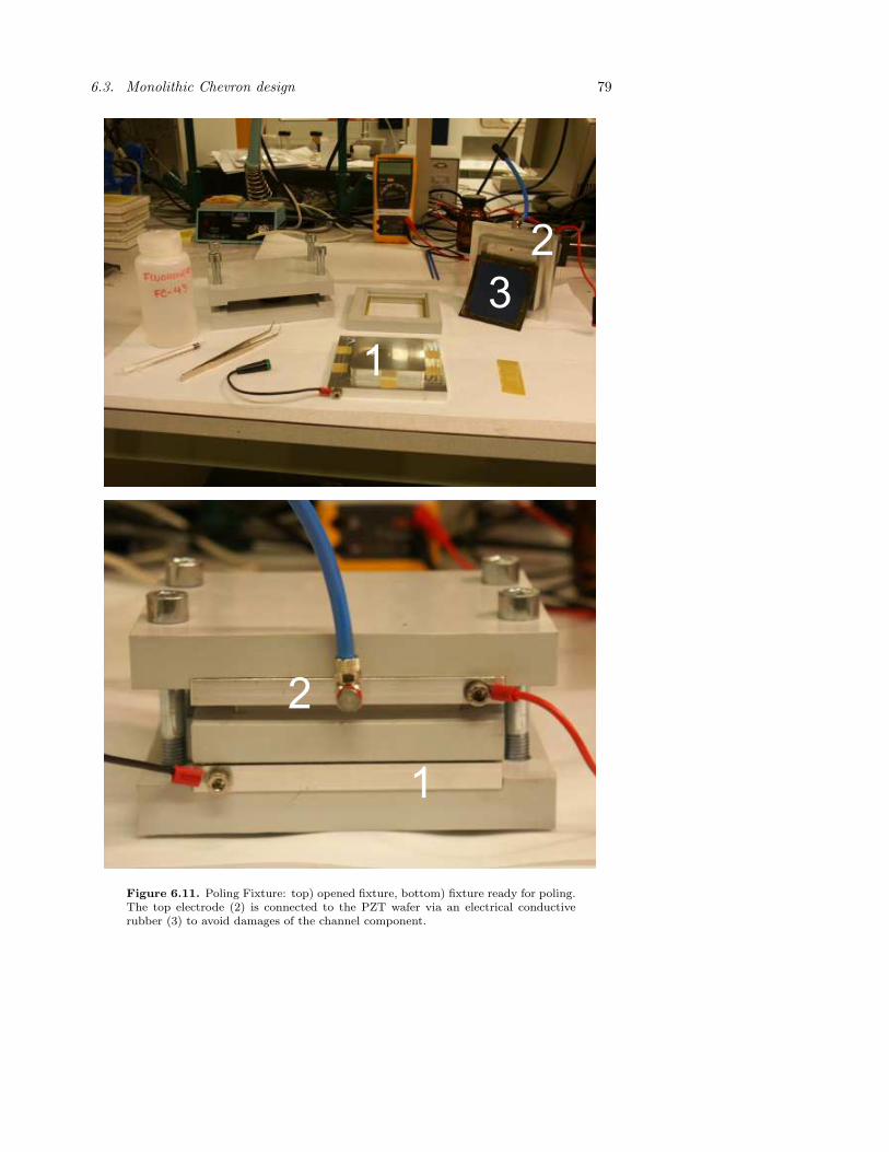
6.3. Monolithic Chevron design 79
1
2
3
1
2
Figure 6.11. Poling Fixture: top) opened fixture, bottom) fixture ready for poling.The top electrode (2) is connected to the PZT wafer via an electrical conductiverubber (3) to avoid damages of the channel component.
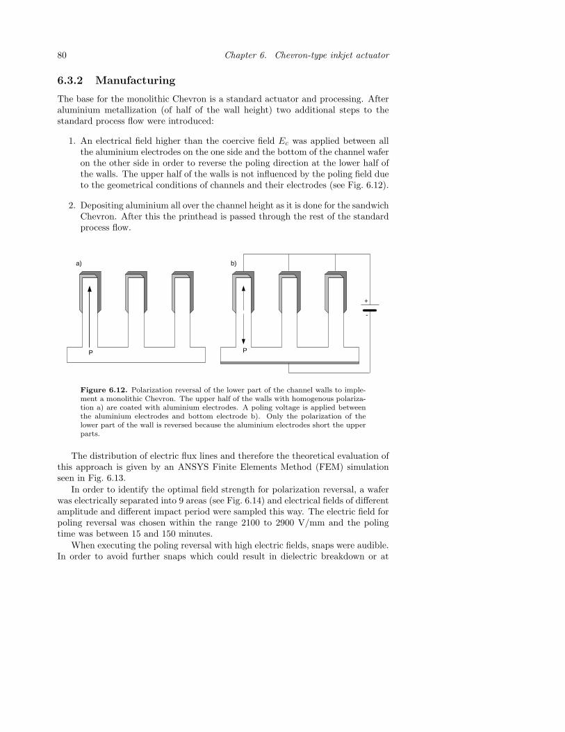
80 Chapter 6. Chevron-type inkjet actuator
6.3.2 Manufacturing
The base for the monolithic Chevron is a standard actuator and processing. Afteraluminium metallization (of half of the wall height) two additional steps to thestandard process flow were introduced:
1. An electrical field higher than the coercive field Ec was applied between allthe aluminium electrodes on the one side and the bottom of the channel waferon the other side in order to reverse the poling direction at the lower half ofthe walls. The upper half of the walls is not influenced by the poling field dueto the geometrical conditions of channels and their electrodes (see Fig. 6.12).
2. Depositing aluminium all over the channel height as it is done for the sandwichChevron. After this the printhead is passed through the rest of the standardprocess flow.
+
-
a) b)
P P
Figure 6.12. Polarization reversal of the lower part of the channel walls to imple-ment a monolithic Chevron. The upper half of the walls with homogenous polariza-tion a) are coated with aluminium electrodes. A poling voltage is applied betweenthe aluminium electrodes and bottom electrode b). Only the polarization of thelower part of the wall is reversed because the aluminium electrodes short the upperparts.
The distribution of electric flux lines and therefore the theoretical evaluation ofthis approach is given by an ANSYS Finite Elements Method (FEM) simulationseen in Fig. 6.13.
In order to identify the optimal field strength for polarization reversal, a waferwas electrically separated into 9 areas (see Fig. 6.14) and electrical fields of differentamplitude and different impact period were sampled this way. The electric field forpoling reversal was chosen within the range 2100 to 2900 V/mm and the polingtime was between 15 and 150 minutes.
When executing the poling reversal with high electric fields, snaps were audible.In order to avoid further snaps which could result in dielectric breakdown or at
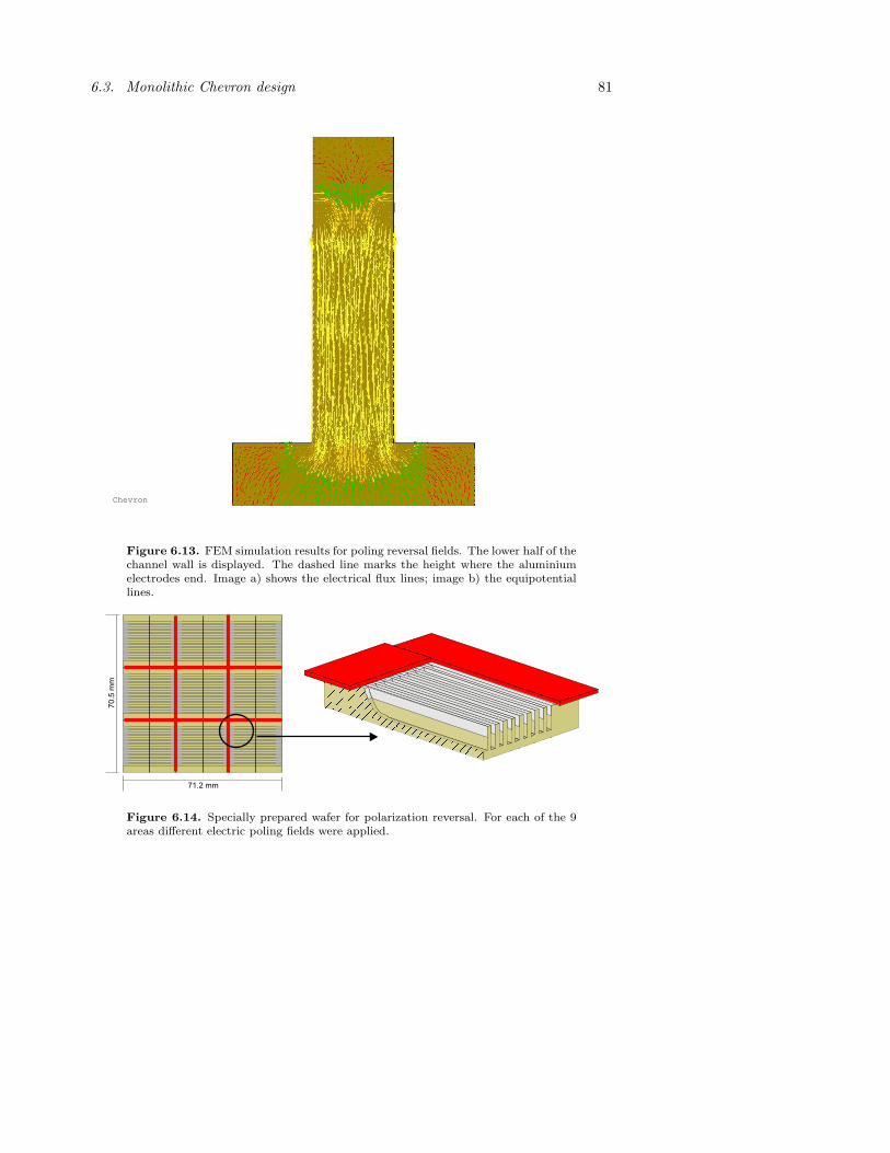
6.3. Monolithic Chevron design 81
Chevron
Figure 6.13. FEM simulation results for poling reversal fields. The lower half of thechannel wall is displayed. The dashed line marks the height where the aluminiumelectrodes end. Image a) shows the electrical flux lines; image b) the equipotentiallines.
71.2 mm
70.5
mm
Figure 6.14. Specially prepared wafer for polarization reversal. For each of the 9areas different electric poling fields were applied.
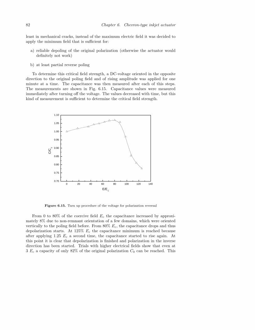
82 Chapter 6. Chevron-type inkjet actuator
least in mechanical cracks, instead of the maximum electric field it was decided toapply the minimum field that is sufficient for:
a) reliable depoling of the original polarization (otherwise the actuator woulddefinitely not work)
b) at least partial reverse poling
To determine this critical field strength, a DC-voltage oriented in the oppositedirection to the original poling field and of rising amplitude was applied for oneminute at a time. The capacitance was then measured after each of this steps.The measurements are shown in Fig. 6.15. Capacitance values were measuredimmediately after turning off the voltage. The values decreased with time, but thiskind of measurement is sufficient to determine the critical field strength.
0 20 40 60 80 100 120 140 0.70
0.75
0.80
0.85
0.90
0.95
1.00
1.05
1.10
C/C
0
E/E C
Figure 6.15. Turn up procedure of the voltage for polarization reversal
From 0 to 80% of the coercive field Ec the capacitance increased by approxi-mately 8% due to non-remnant orientation of a few domains, which were orientedvertically to the poling field before. From 80% Ec, the capacitance drops and thusdepolarization starts. At 125% Ec the capacitance minimum is reached becauseafter applying 1.25 Ec a second time, the capacitance started to rise again. Atthis point it is clear that depolarization is finished and polarization in the inversedirection has been started. Trials with higher electrical fields show that even at3 Ec a capacity of only 82% of the original polarization C0 can be reached. This
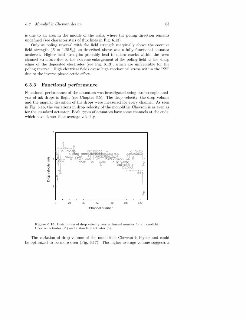
6.3. Monolithic Chevron design 83
is due to an area in the middle of the walls, where the poling direction remainsundefined (see characteristics of flux lines in Fig. 6.13)
Only at poling reversal with the field strength marginally above the coercivefield strength (E = 1.25Ec), as described above was a fully functional actuatorachieved. Higher field strengths probably lead to micro cracks within the sawnchannel structure due to the extreme enlargement of the poling field at the sharpedges of the deposited electrodes (see Fig. 6.13), which are unfavorable for thepoling reversal. High electrical fields cause high mechanical stress within the PZTdue to the inverse piezoelectric effect.
6.3.3 Functional performance
Functional performance of the actuators was investigated using stroboscopic anal-ysis of ink drops in flight (see Chapter 3.5). The drop velocity, the drop volumeand the angular deviation of the drops were measured for every channel. As seenin Fig. 6.16, the variations in drop velocity of the monolithic Chevron is as even asfor the standard actuator. Both types of actuators have some channels at the ends,which have slower than average velocity.
0 20 40 60 80 100 120
5
6
7
Dro
p ve
loci
ty, m
/s
Channel number
Figure 6.16. Distribution of drop velocity versus channel number for a monolithicChevron actuator (4) and a standard actuator ().
The variation of drop volume of the monolithic Chevron is higher and couldbe optimized to be more even (Fig. 6.17). The higher average volume suggests a
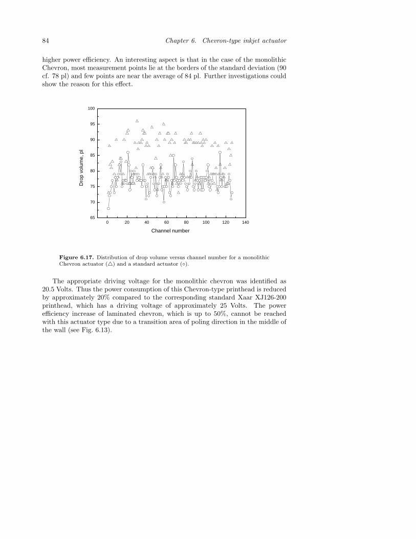
84 Chapter 6. Chevron-type inkjet actuator
higher power efficiency. An interesting aspect is that in the case of the monolithicChevron, most measurement points lie at the borders of the standard deviation (90cf. 78 pl) and few points are near the average of 84 pl. Further investigations couldshow the reason for this effect.
0 20 40 60 80 100 120 140 65
70
75
80
85
90
95
100
Dro
p vo
lum
e, p
l
Channel number
Figure 6.17. Distribution of drop volume versus channel number for a monolithicChevron actuator (4) and a standard actuator ().
The appropriate driving voltage for the monolithic chevron was identified as20.5 Volts. Thus the power consumption of this Chevron-type printhead is reducedby approximately 20% compared to the corresponding standard Xaar XJ126-200printhead, which has a driving voltage of approximately 25 Volts. The powerefficiency increase of laminated chevron, which is up to 50%, cannot be reachedwith this actuator type due to a transition area of poling direction in the middle ofthe wall (see Fig. 6.13).

6.4. Conclusions 85
6.4 Conclusions
Two types of Chevron actuators have been made: Laminated Chevron and Mono-lithic Chevron. Pros and cons of both types are listed beneath in a short summary.
Laminated Chevron
+ power consumption of the printhead reduced by 50%;
+ improved homogeneity of the drop velocity within the actuator;
- good control of the glue layer thickness required;
- additional machining and gluing steps are necessary to produce the Chevronsandwich wafer;
- waste of expensive PZT material.
Monolithic Chevron
+ power consumption of the printhead reduced by 20% but less than the lami-nated Chevron with 50%;
+ just one additional metallization step is necessary and no extra machining ofthe PZT wafer is required;
- the ratio between top and bottom polarization part is dependent on the elec-trode depth after the first metallization;
- the mechanism of polarization reversal still not fully under control;
- time consuming process due to slow heating and cooling rate during polariza-tion reversal.

86
Chapter 7
Summary of results
This section summarizes each appended paper and manuscript and also states thedegree of my participation.
7.1 “Dielectric and Pulsed Spectroscopy of ShearMode PZT Microactuator”
We examined the dielectric and mechanical properties of shear mode actuators.The measurements were done with an HP4194A Impedance Analyzer, a Fluke 6304RCL meter, and a new pulsed technique, developed to characterize this type ofactuators. Temperature dependencies of the properties were investigated as well.My contributionI prepared the samples, made the measurements and participated in the analysisand preparation of the manuscript.
7.2 “Non destructive Pulsed Technique to Char-acterize Functional Properties of MicromachinedBulk PZT”
This paper describes a non-destructive pulsed technique we have developed to char-acterize micromachined PZT ceramics. Dielectric properties and mechanical reso-nance behaviour of the actuators are measured and evaluated to obtain dielectricpermittivity and losses, Curie temperature, mechanical quality factor, and reso-nance frequencies. Furthermore, we investigated fatigue in the PZT material dueto high electric fields.
87
88 Chapter 7. Summary of results
My contributionI prepared the samples, made the measurements and participated in the analysisand preparation of the manuscript.
7.3 “Thermometry Inside Inkjet Actuators”
We present a new method to measure the temperature inside the inkjet actuators.In this technique ‘dummy walls’ located at the beginning and the end of a PZTchannel wall array are used as sensing elements. Temperature changes inside theactuator will cause a change in the dielectric permittivity which can be measuredas change in the capacitance of the ‘dummy walls’. In this way we monitor the tem-perature at different printing conditions and in different printhead designs. Moredetails are given in Chapter 5.My contributionI prepared parts of the samples, made measurements and participated in the anal-ysis and preparation of the manuscript.
7.4 “Piezoelectric shear mode inkjet actuator”
This paper gives a survey of different printing techniques such as continuous jet,thermal jet and different techniques using piezoelectric actuators. More extensivelythe Xaar-type piezoelectric shear mode actuator is studied and characterized. In-formation about the manufacturing techniques are given. Characterizations thathave been made are pulsed technique, ferroelectric hysteresis loop tracing and di-electric spectroscopy. The main resonance frequencies were found both by usingdielectric spectroscopy and pulsed technique. Furthermore, PZT materials fromdifferent manufacturers were compared.My contributionI prepared the samples, made the measurements and the analysis and prepared themanuscript.
7.5 “Piezoelectric shear mode drop-on-demand ink-jet actuator”
This review paper starts with an introduction into the field of inkjet printing by abrief description of the common technologies. We emphasize on Xaar -type shearmode actuators by giving details on their design and manufacturing methods. Inthe following we comprehensively characterize the actuators by dielectric and pulsedspectroscopy as well as ferroelectric hysteresis loop tracing and investigate the print-ing performance by stroboscopy. Furthermore, resonance characteristics of the ac-tuators are investigated and analyzed.

7.7. “Fatigue of shear mode PZT actuator” 89
My contributionI prepared the samples, made the measurements and participated in the analysisand preparation of the manuscript.
7.6 ““Chevron”-type piezoelectric inkjet actuator”
We investigated resonance characteristics and functional performance of two typesof inkjet actuators. Both types were based on the shared wall principle of Xaarinkjet printheads. In the standard type the channels walls have only one polingdirection whereas in the Chevron-type the walls have two opposite directions of thepolarization in the upper and lower halves of the wall. Fundamental resonancesof the channel walls were detected by means of admittance spectroscopy with anHP4194A analyzer and a pulsed technique. Functional performance was tested bystroboscopic technique.My contributionI prepared the samples, made the measurements and the analysis and prepared themanuscript.
7.7 “Fatigue of shear mode PZT actuator”
Bulk wafers of polarized PZT ceramics were micromachined by sawing grooves witha high precision diamond saw to fabricate an array of channel walls. Stroboscopictests were performed to quantify the ultimate inkjet performance: ink-drop velocityand volume. The temperature dependence of the dielectric permittivity was mea-sured by an LCR meter and a novel pulsed technique. Ferroelectric hysteresis P-Eloops were traced with a Sawyer-Tower circuit. The channel walls were subjectedto electrical treatment (aging) by tracing of ferroelectric hysteresis P-E loops witha triangular shaped electric field. The high voltage treatment influences materialproperties (fatigue effect) seen in a change of the P − E loops with the number ofcycles. After 90,000 electric field cycles Pr decreased whereby Ec increased.My contributionI prepared the samples, made the measurements and participated in the analysisand preparation of the manuscript.

90
Bibliography
[1] F. R. S. Rayleigh. On the instability of jets. Proc. London Math. Soc., 10(4):4–13, 1878.
[2] R. Elmqvist. Measuring instrument of the recording type. U.S. Patent no.2,566,443, 1948.
[3] R.G. Sweet. Signal apparatus with fluid drop recorder. U.S. Patent no.3,596,275, 1971.
[4] W. L. Buehner, J. D. Hill, T. H. Williams, and J. W. Woods. Applicationof ink-jet technology to a word processing output printer. IBM J. Res. Dev.,21:2–9, 1977.
[5] S. L. Zoltan. Pulse droplet ejection system. U.S. Patent no. 3,857,049, CleviteCorp., 1974.
[6] I. Endo, Y. Sato, S. Saito, T. Nakagiri, and O. Ohno. Liquid jet recordingprocess and apparatus therefor. Great Britain Patent no. 2,007,162, Canon,1979.
[7] J. L. Vaught, F. L. Cloutier, D. K. Donald, J. D. Meyer, C. A. Tacklind, andH. H. Taub. Thermal ink-jet printer. U.S. Patent no. 4,491,728, Hewlett-Packard, 1984.
[8] H. P. Le. Progress and trends in ink-jet printing technology. Journal of ImagingScience and Technology, 42:42–62, 1998.
[9] F. J. Kampfhoefner. Ink-jet printing. IEEE Trans. Elec. Devices, ED19:584,1972.
[10] L. Kuhn and A. Myers. Ink-jet printing. Scientific America, 240:162–178,1979.
[11] W. Wehl. Nur nicht kleckern. CHIP, 8:104–112, 1994.
[12] H. H. Taub and P. H. Wolf. Ink jet head structure. U.S. Patent no. 4,306,243,DataProducts Corp., 1918.
91
92 Bibliography
[13] T. Goldman and J. S. Gonzales. DNA-printing: utilization of a standard inkjetprinter for the transfer of nucleic acids to solid supports. J. Biochem. Biophys.Methods, 42:105–110, 2000.
[14] G. Percin, T. Lundgren, and B. Khuri-Yakub. Controlled ink-jet printing anddeposition of organic polymers and solid particles. Appl. Phys. Lett, 73:No.16,1998.
[15] W. Voit, K. V. Rao, and W. Zapka. Direct-write process for UV-curable epoxymaterials by inkjet technology. page LL3.5.1. in Mat. Res. Soc. Symp. Proc.758.
[16] W. G. Hawkins. Bubble jet priniting device. U.S. Patent no. 4,523,530, XeroxCorp., 1985.
[17] E. L. Kyser and S. B. Sears. Method and apparatus for recording with writingfluids and drop projection means therefor. U.S. Patent no. 3,946,398, SiliconicsInc., 1976.
[18] A. Mikalesen. Apparatus and method employing phase change ink. U.S. Patentno. 4,742,364, DataProducts Corp., 1988.
[19] W. S. Bartky, A. D. Paton, S. Temple, and A. J. Michaelis. Droplet depositionapparatus. U.S. Patent no. 4,879,568, Xaar, 1989.
[20] G. Beurer and J. Kretschmer. Function and performance of a shear mode piezoprinthead. In International Conference on Digital Printing Technologies NIP13, pages 621–625. IS&T, October 1997.
[21] H. J. Manning and R. A. Harvey. Xaar greyscale technology. In InternationalConference on Digital Printing Technologies NIP 15, pages 35–39. IS&T, Oc-tober 1999.
[22] http://www.epson.com.
[23] http://www.xaar.co.uk. April, 17th 2003.
[24] Rolf Kaack. Large drop actuators. Master’s thesis, University of Freiburg,Germany, July 2001.
[25] N. Aurell, D. Roche, C. Richard, and P. Gonnard. Sample aspect ratio influenceon the shear coefficients measurements of a piezoelectric bar. In Proceedingsof the Ninth IEEE International Symposium on Applications on Ferroelectrics,pages 162–165. ISAF ’94/IEEE, 1994.
[26] A. Ballato. Piezoelectricity: Old effect, new thrust. IEEE Transactions onUltrasonics, Ferroelectrics and Frequency Control, 42:916–926, 1995.
Bibliography 93
[27] J. R. Phillips. Piezoelectirc technology primer. Technical report, CTS WirelessComponents.
[28] Yuhuan Xu. Ferroelectric materials and their applications. North-Holland,1991.
[29] Standrad on piezoelectricity. ANSI/IEEE Standard 176-1987, 1988.
[30] Standrad definitions and methods of measuring for piezoelectric vibrators.ANSI/IEEE Standard 177, 1966.
[31] C. M. Harris and C. E. Crede. Shock and Vibration Handbook. Chapter 7.McGraw-Hill, New York, 4th edition, 1995.
[32] M. E. Lines. Principles and applications of ferroelectrics and related materials,page 102. Oxford University Press, Clarendon, 1977.
[33] Jurgen Brunahl. Incorporating a PZT thermosensor into a XaarJet print-head for on-line temperature compensation. Master’s thesis, FachhochschuleZweibrucken, Germany, 1999.
[34] A. Jorzick and W. Zapka. Real-time temperature measurement inside a print-head actuator. In The Eigth International Conference on new Actuators, Ac-tuator 2002, pages . 138–140, 2002.
[35] Thomas Jager. Investigation and characterization of special ink-jet actuators.Master’s thesis, Albert-Ludwigs-University of Freiburg, Germany, 2002.

Index
acousticcompression wave, 13periode, 13rarefaction wave, 13
actuatorbend mode, 9Chevron-type, see Chevronpush mode, 9shear mode, 11squeeze mode, 8
admittance, 35angular deviation, 15, 83ANSYS, 19
base plate, 11, 69bend mode, see actuatorbonding, 72Bubble-Jet, 7
capacitance, 34, 59Chevron, 69
active layer, 73alternative bonding, 77glue joint, 73laminated, 71
FEM, 76glue joint, 77manufacturing, 71
monolithicdesign, 78FEM, 80manufacturing, 80
slanted, 73coercive field, 27, 82conductive rubber, 78
coupling coefficient, 28, 37, 38cover bonding, 14cover plate, 11, 69
AlN, 65Curie temperature, 14, 23, 28, 48, 60Curie-Weiss
constant, 28law, 28, 47
d15, see piezoelectric coefficientdepolarization, 82design
shear mode, 11dicing, 14dielectric
constant, 27, 59, 60loss, 27, 33, 47, 48permittivity, 27, 33, 47, 48spectroscopy, 33, 47, 48
dipol, 24reorientation, 50rotation, 50
domain, 24boundary, 24
dpi, 15dressing, 73driving voltage, 12, 58, 84drop
generation, 12lead-, 42satellite-, 42velocity, 15, 18, 43, 57, 83volume, 15, 17, 43, 83
dummy channel, 58, 61dY, 37
94

Index 95
electrode, 69electrodes, 12, 13
Fast Fourier Transform, see FFTfatigue, 50FEM, 19ferroelectric, 28
fatigue, see fatigueFFT, 39Finite Element Method, see FEMFluke PM6304, 33, 47
HP4194 Impedance Analyser, 35HP4194A Impedance Analyzer, 48, 53,
74hysteresis, 26, 50
measurement, 40
impedance, 34, 35ink
channels, 11inlet, 12, 63
inkjetcontinuous, 6drop-on-demand, 7history, 5piezoelectric, 8thermal, 7
lamination, 72lead zirconate titanate, see PZT
manufacturingshear mode, 13
MEMS, 7, 23metallization, 13
Chevron, 80
nozzlediameter, 19plate, 12
nozzle plate, 14
paraelectric, 28passivation, 14, 76
phase transition, 28piezoelectic
piezoelectricity, 29piezoelectric
coefficient, 17, 29directions, 29effect, 17, 23, 29, 36, 38inverse effect, 23, 36
polarization, 26, 50, 82Chevron, 71direction, 12microscope, 50remnant, 26, 27, 50reversal, 78, 80set-up, 78standard, 69
poling, 26de-, 26direction, 80electrodes, 26field, 26field strength, 82
polishing, 72power consumption, 69, 85pressure in channel, 16pulsed spectroscopy, 38, 47, 48, 53push mode, see actuatorPZT, 11, 23, 30
history, 23machining, 13
quality factor, 34
reactance, 34resistance, 34resolution, 15resonance
acoustic modes, 53analysis, 19frequency, 19, 35, 38, 39, 48, 53
parallel, 37serial, 37
test, 35
Sawyer-Tower circuit, 40

96 Index
sheardisplacement, 12, 30strain, 31
squeeze mode, see actuatorStroboscopy, 42stroboscopy, 55, 83
tanδ, see dielectric losstemperature
compensation, 57, 58sensor, 57
thermal conductivity, 65thermistor, 58thermometry, 57
viscosity, 57voltage divider circuit, 61
Xaar actuator, see shear mode

Appendix A
PZT piezoelectric materialstechnical data
97