Physics of Materials: Carbon Materials: History and...
51
Physics of Materials Dr. Anurag Srivastava Atal Bihari Vajpayee Indian Institute of Information Technology and Manegement, Gwalior Physics of Materials: Carbon Materials: History and Allotropes
Transcript of Physics of Materials: Carbon Materials: History and...

Physics of Materials
Dr. Anurag SrivastavaAtal Bihari Vajpayee
Indian Institute of Information Technology and
Manegement, Gwalior
Physics of Materials:
Carbon Materials: History and
Allotropes

ABV- IIITM-Gwalior (MP) IndiaPhysics of Materials
All living things on Earth contain
carbon. But, what is carbon?
Why is it important?

ABV- IIITM-Gwalior (MP) IndiaPhysics of Materials
Carbon is found all over the Earth.
It is an element. It is in the air, in the ocean, in the Earth’s
crust.
If carbon is mixed with other elements you get; limestone,
chalk, marble, coal, gas, alcohol, sugars, fats, and even
medicines. The black stuff in your pencil, graphite, is
carbon. Diamonds are 100% pure carbon. Your body even
contains carbon, the same stuff from which diamonds are
made!
Carbon is inside of us, outside of us, and right now you are
breathing out carbon (in the form of a gas: carbon dioxide).
Carbon is everywhere.
ABV- IIITM-Gwalior (MP) IndiaPhysics of Materials
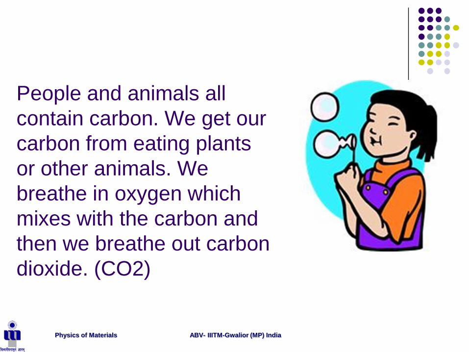
People and animals all
contain carbon. We get our
carbon from eating plants
or other animals. We
breathe in oxygen which
mixes with the carbon and
then we breathe out carbon
dioxide. (CO2)

ABV- IIITM-Gwalior (MP) IndiaPhysics of Materials
Carbon Element
We have learnt carbon element as the basis
of Organic Chemistry.
Why does carbon can form so many different
compounds?
Carbon is found the second period group
IVA of the periodic table.
ABV- IIITM-Gwalior (MP) IndiaPhysics of Materials
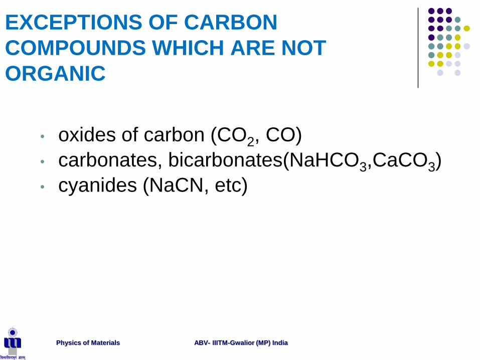
EXCEPTIONS OF CARBON
COMPOUNDS WHICH ARE NOT
ORGANIC
• oxides of carbon (CO2, CO)
• carbonates, bicarbonates(NaHCO3,CaCO3)
• cyanides (NaCN, etc)
ABV- IIITM-Gwalior (MP) IndiaPhysics of Materials
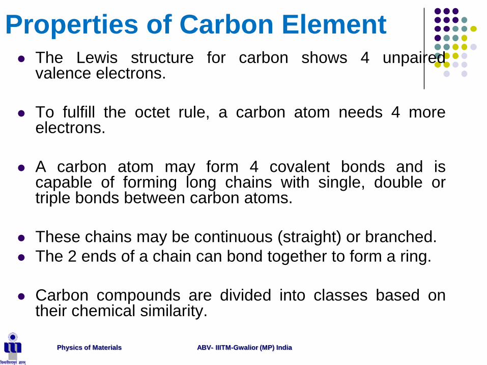
Properties of Carbon Element The Lewis structure for carbon shows 4 unpaired
valence electrons.
To fulfill the octet rule, a carbon atom needs 4 moreelectrons.
A carbon atom may form 4 covalent bonds and iscapable of forming long chains with single, double ortriple bonds between carbon atoms.
These chains may be continuous (straight) or branched.
The 2 ends of a chain can bond together to form a ring.
Carbon compounds are divided into classes based ontheir chemical similarity.

ABV- IIITM-Gwalior (MP) IndiaPhysics of Materials
Hydrocarbons Hydrocarbons are compounds containing hydrogen and
carbon. Hydrocarbons may have different numbers ofbonds between carbon atoms.
The four hydrocarbon classes are: alkane (single bond),
alkene, (double bond),
alkyne (triple bond),
aromatic (benzene ring).
Alkanes contain only single C-C bonds. They contain asmany hydrogen atoms as possible, and are said to besaturated.
Hydrocarbons containing double or triple bonds areunsaturated.
A homologous series is series of compounds that differ bya constant increment. Aromatic hydrocarbons include abenzene ring- 6 carbon atoms with all the bondsalternating between a single and a double bond.

ABV- IIITM-Gwalior (MP) IndiaPhysics of Materials
Properties of Carbon Element
Carbon is unique
It has 6 electrons in its outer
shell arranges 1s22s2sp2
It has room for 4 bonds to 4
other atoms.
Carbon-to-carbon bonds can
be single (A),
double (B), or
triple (C).
Note: In each example, each
carbon atom has four
dashes, which represent four
bonding pairs of electrons,
satisfying the octet rule.

ABV- IIITM-Gwalior (MP) IndiaPhysics of Materials
Alkanes Alkenes Alkynes
SATURATED means that each carbon is bonded to four other atoms through single covalent bonds. Hydrogen atoms usually occupy all available bonding positions after the carbons have bonded to each other.
UNSATURATED hydrocarbons contain either double or triple bonds. Since the compound is unsaturated with respect to hydrogen atoms, the extra electrons are shared between 2 carbon atoms forming double or triple bonds.
PARAFFINS which is derived from a Latin word meaning "little activity", and means that the compounds are very unreactive.
Alkenes are also called OLEFINS because they form oily liquids on reaction with chlorine gas.
Alkynes are also generally known as ACETYLENES from the first compound in the series.
HYDROCARBONS

ABV- IIITM-Gwalior (MP) IndiaPhysics of Materials
Hydrocarbons
C C C C
C C
C
C
C
C
C
C
H
H
H
H
H
H
C C C C C
H
H
H
H
H H
H
H
H
H
H
H
Alkanes Alkenes
Alkynes Aromatics
C C C C C
H
H
H
H
H
H
H
H
H
H
C C C C CH
H
H
H
H
H
H
H

ABV- IIITM-Gwalior (MP) IndiaPhysics of Materials
Properties of Carbon Element
A)The carbon atom forms
bonds in a tetrahedral
structure with a bond angle
of 109.5O.
(B) Carbon-to-carbon bond
angles are 109.5O, so a
chain of carbon atoms
makes a zigzag pattern.
(C) The unbranched chain of
carbon atoms is usually
simplified in a way that
looks like a straight chain,
but it is actually a zigzag, as
shown in (B).
ABV- IIITM-Gwalior (MP) IndiaPhysics of Materials
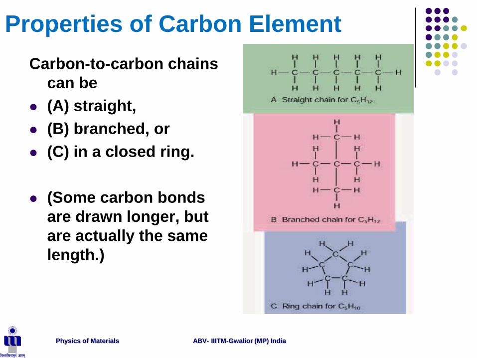
Properties of Carbon Element
Carbon-to-carbon chains
can be
(A) straight,
(B) branched, or
(C) in a closed ring.
(Some carbon bonds
are drawn longer, but
are actually the same
length.)

ABV- IIITM-Gwalior (MP) IndiaPhysics of Materials
Why does carbon can form so many
different compounds? Carbon's ability to form long carbon-to-carbon chains is the first of five
reasons that there can be so many different carbon compounds; a molecule that differs by even one atom is, of course, a molecule of a different compound.
The second reason for carbon's astounding compound-forming ability is that carbon atoms can bind to each other not only in straight chains, but in complex branchings, like the branches of a tree.
They can even join "head-to-tail" to make rings of carbon atoms.
There is practically no limit to the number or complexity of the branches or the number of rings that can be attached to them, and hence no limit to the number of different molecules that can be formed.
The third reason is that carbon atoms can share not only a single electron with another atom to form a single bond, but it can also sharetwo or three electrons, forming a double or triple bond.
This makes for a huge number of possible bond combinations at different places, making a huge number of different possible molecules.
And a molecule that differs by even one atom or one bond position is a molecule of a different compound.
ABV- IIITM-Gwalior (MP) IndiaPhysics of Materials
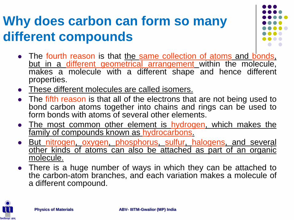
Why does carbon can form so many
different compounds
The fourth reason is that the same collection of atoms and bonds,but in a different geometrical arrangement within the molecule,makes a molecule with a different shape and hence differentproperties.
These different molecules are called isomers.
The fifth reason is that all of the electrons that are not being used tobond carbon atoms together into chains and rings can be used toform bonds with atoms of several other elements.
The most common other element is hydrogen, which makes thefamily of compounds known as hydrocarbons.
But nitrogen, oxygen, phosphorus, sulfur, halogens, and severalother kinds of atoms can also be attached as part of an organicmolecule.
There is a huge number of ways in which they can be attached tothe carbon-atom branches, and each variation makes a molecule ofa different compound.

ABV- IIITM-Gwalior (MP) IndiaPhysics of Materials
The Greater Stability of C-C Bonds
Since the average bond dissociation
energy of C-C is greater than the
average bond energies between
different atoms.
Thus the energy released when
carbon atom bonds to another
carbon atom is greater than the
energy released when the other
atoms like B,N,O,Si,P and S bonds
to each other.
Thus C-C bond is more stable than
the others like B-B,N-N,
O-O,Si-Si,P-P and S-S.
Bonding Atoms
Bond Energy (kJ mol
-1)
B-B 293 C-C 343 N-N 163 O-O 157 Si-Si 222 P-P 201 S-S 266
ABV- IIITM-Gwalior (MP) IndiaPhysics of Materials
Ability to Form Chains Between
Their Atoms
The atoms closer to C in the periodic table are B,N,O,Si,P and S.
The ability of these atoms to bond each other to form chains is lower than C.
For examle Si can produce chains made of at most 11 atoms of it and N at most three atoms it.
Although the ability to form chains between their atoms for P and S is greater than Si and N but it is very much smaller compared to C.

ABV- IIITM-Gwalior (MP) IndiaPhysics of Materials
Ability to Form Chains Between
Their Atoms
The greater ability of carbon to form chains compared to atoms
closer to it in the periodic table can be explained by two reasons:
1. The average bond dissociation energies of them is lower than
that of carbon.
2. The electronegativity values B,Si and P lower than that of
C.atoms.Thus the attraction forces between these atoms are
smaller than that of carbon.This is also true when these atoms
are bonded to the other atoms like hydrogen or halogens.
Li Be B C N O F 1,0 1,5 2,0 2,5 3,0 3,5 4,0 Na Mg Al Si P S Cl
0,9 1,3 1,6 1,9 2,2 2,5 3,2 Electronegativity values of some elements ording to Pauling’s Scale

ABV- IIITM-Gwalior (MP) IndiaPhysics of Materials
Electronegativity
Electronegativity:
a measure of an atom’s attraction for the
electrons it shares with another atom in a
chemical bond
Pauling scale
generally increases left to right in a row
generally increases bottom to top in a column

ABV- IIITM-Gwalior (MP) IndiaPhysics of Materials
Greater Bonding Capacity of C compared to
N and O
The electronegativity values of N and O are greater than that of C.But their bonding capacities are smaller than that of C since
they have lower number of unpaired electrons.
Lewis Dot Diagrams of Selected Elements

ABV- IIITM-Gwalior (MP) IndiaPhysics of Materials
Summary…
Compared to C atom B,Si,P,N and O atoms
can not be expected to form greater number
of compounds and unbrached and branched
chains and cyclic compounds.
Carbon compounds are more stable than
Si4,P4,O3,S8 and B4 molecules.

ABV- IIITM-Gwalior (MP) IndiaPhysics of Materials
Carbon Allotropes
Fullerenes
Carbon nanotubes
Graphene
Diamond
ABV- IIITM-Gwalior (MP) IndiaPhysics of Materials
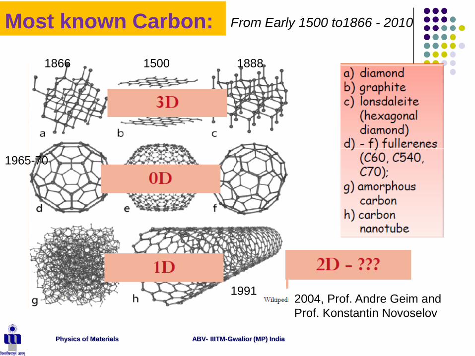
Most known Carbon: From Early 1500 to1866 - 2010
15001866 1888
1965-70
19912004, Prof. Andre Geim and
Prof. Konstantin Novoselov

ABV- IIITM-Gwalior (MP) IndiaPhysics of Materials
Graphene: The mother of all Graphites
Graphene is a 2D building material for carbon materials of all other dimensionalities. It can be
wrapped up into 0D buckyballs, rolled into 1D nanotubes or stacked into 3D graphite.

ABV- IIITM-Gwalior (MP) IndiaPhysics of Materials
Fullerenes
Discovered in 1985 at Rice Univ. and Univ. Essex
Includes CNTs, buckyballs, and derivatives
C60 most common, but other forms exits (C70, C100, C400)
The number of carbon atoms (Nc) in molecule can determine
its structure (based on molecular orbital theory calculations)
Nc odd: linear or ring
Nc even: cage-like
Fulleranes: hydrogenated form of fullerene
C60 C70

ABV- IIITM-Gwalior (MP) IndiaPhysics of Materials
Fullerene Properties (C60)
Truncated icosahedron with 32 faces, 90 edges, 60
vertices
20 hexagonal faces
12 pentagonal faces
Diameter : 7.10 Å
Bonds in fullerenes: sp2–sp3 admixture
Bonding between fullerenes
Noncovalent
van der Waals
- interactions
Covalent

ABV- IIITM-Gwalior (MP) IndiaPhysics of Materials
Fullerene synthesis
Arc discharge plasma
High current applied between two graphite electrodes in
He environment
Carbon vaporizes and fullerenes collects on cathode
CNTs form if metal catalyst included in graphite
Low purity: ~ 15% C60
Laser ablation
Graphite target exposed to extremely high temperatures
Produces higher order fullerenes
Combustion of hydrocarbon fuel under low
pressure
Requires least amount of energy
Produces most pure products

ABV- IIITM-Gwalior (MP) IndiaPhysics of Materials
Fullerene modification
Endohedral
Enclosed chemical
species
X@C60
Exohedral
Functionalization
Fullerene structures
Fullerene crystals
fcc structure held
together by vdW forces
Arrays
fcc fullerene crystal
Endohedral fullerenes
Exohedral fullerenes
ABV- IIITM-Gwalior (MP) IndiaPhysics of Materials
Recent Progress - Fullerenes
Fulleride superconductor: 38 K Tc Cs3C60
Physical Review Letters, v 101, n 13, 26 Sept. 2008, p 136404 (4 pp.)
Electrospray deposition of C60
Journal of Physical Chemistry C, v 112, n 20, 22 May 2008, p 7706-9
Bottom-contact fullerene C60 thin-film transistors with high field-effect mobilities
Applied Physics Letters, v 93, n 3, 21 July 2008, p 033313-1-3
Mechanics of spheroidal fullerenes and carbon nanotubes for drug and gene delivery
Quarterly Journal of Mechanics and Applied Mathematics, v 60, pt.2, May 2007, p 231-48
Applications of fullerene beams in analysis of thin layers
Vacuum, v 82, n 10, 3 June 2008, p 1120-3

ABV- IIITM-Gwalior (MP) IndiaPhysics of Materials
Carbon Nanotubes (CNTs)
Single-walled CNTs (SWCNTs)
Graphene sheet rolled into a tube
Forms of SWCNTs
Zigzag
Armchair
Chiral
Multiwalled CNTs (MWCNTs)
Series of concentric SWCNTs

ABV- IIITM-Gwalior (MP) IndiaPhysics of Materials
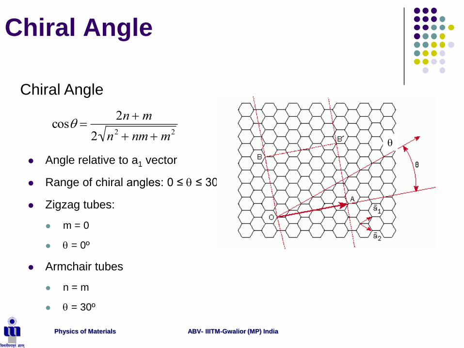
Vector Notation for SWCNTs
Description of SWCNTs structure
a1 and a2: unit base cell vectors
n ≥ m
|a1| = |a2| = 0.246 nm
Bond length b = a/√3 = 0.142
Notation: (n, m)
Point (0,0) connected to (n, m)
dSWCNT a n2 nmm2
C = na1 + ma2
a1 and a2: unit base cell vectors
Chiral Vector
Diameter
ABV- IIITM-Gwalior (MP) IndiaPhysics of Materials
Chiral Angle
Angle relative to a1 vector
Range of chiral angles: 0 ≤ ≤ 30º
Zigzag tubes:
m = 0
= 0º
Armchair tubes
n = m
= 30º
Chiral Angle
cos 2n m
2 n2 nm m2

ABV- IIITM-Gwalior (MP) IndiaPhysics of Materials
Nanotube structure and chiral
vector

ABV- IIITM-Gwalior (MP) IndiaPhysics of Materials
Electrical Properties
Metallic SWCNTs
Conduction is quantized (m.f.p. of electrons on order of dimensions
of tubes
Ballistic transport (no scattering)
In theory can carry electrical current density 1000x silver or copper
|(n-m)| = 3q where q is an integer
Criteria for conduction:
All armchair tubes (n = m)
All zigzag with n multiple of 3
Chiral tubes that meet above criteria
• Semiconducting SWCNTs
– |(n-m)|≠3q

ABV- IIITM-Gwalior (MP) IndiaPhysics of Materials
Other properties of SWCNTs
Thermal conductivity
Thermal conductivity along axis is greater than around
circumference
~ 6000 W/m•K along axis (Copper ~ 385 W/m•K) at room T
Optical
Band gap of semiconducting tubes (0.4 to 0.7 eV)
Eg ~ 5.4b/dSWCNT
b: bond length
d: diameter

ABV- IIITM-Gwalior (MP) IndiaPhysics of Materials
Synthesis of CNTs
Regarded as the best method
Requires little energy (T ~ 100s ºC)
Carbon source broken apart in presence of metal catalyst
Carbon sources for CVD Methane
Acetylene
Ethylene
CO
Polydisperse products (bad!) Diameter
Chirality
Length
Orientation
No one has been able to synthesize exactly one kind of nanotube at a time
Synthesis of SWCNT vs. MWCNTs Control deposition conditions (P, T, gas composition, catalyst composition and
size)
SWCNTs with chemical vapor deposition

ABV- IIITM-Gwalior (MP) IndiaPhysics of Materials
Growth mechanism of CNTs
Base-growth
Typical of SWCNTs
Catalyst remains anchored to substrate (usually alumina)
Tip growth
SWCNTs and MWCNTs
Catalyst comes detached from substrate
Favored for silica type substrates
Limitations to growth
Increased vdW forces between tube and substrate with tube length
Growth terminates when force becomes too great
Application of electric field can enhance growth
Transport of carbon source to catalyst
Diffusion to catalyst from bulk more difficult as tube length increases
Diffusion across catalyst surface inhibited by encapsulation

ABV- IIITM-Gwalior (MP) IndiaPhysics of Materials
History of Graphene Wallace in 1947
Created 2D structure to help in the understanding of 3D
Graphite
Single layers of graphite grown epitaxially on metallic
substrates in the 1970s
Tightly bound to substrate, distorted properties
Term ―graphene‖ coined in 1987
2004, Geim and Novoselov mechanically exfoliated sheets
of graphene from graphite
Transferred to charge neutral silicon substrate
First successful electrical properties measured
Geim, A. K. & MacDonald, A. H. (2007). "Graphene: Exploring carbon flatland".
Physics Today.
ABV- IIITM-Gwalior (MP) IndiaPhysics of Materials
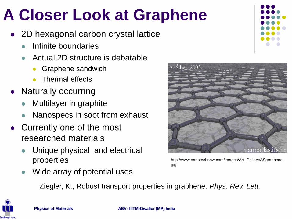
A Closer Look at Graphene 2D hexagonal carbon crystal lattice
Infinite boundaries
Actual 2D structure is debatable
Graphene sandwich
Thermal effects
Naturally occurring
Multilayer in graphite
Nanospecs in soot from exhaust
Currently one of the most
researched materials
Unique physical and electrical
properties
Wide array of potential uses
http://www.nanotechnow.com/images/Art_Gallery/ASgraphene.
jpg
Ziegler, K., Robust transport properties in graphene. Phys. Rev. Lett.
ABV- IIITM-Gwalior (MP) IndiaPhysics of Materials
Graphene Mechanical Properties Breaking strength 200
times greater than steel
Youngs modulus of ~ 1
tPa
Incredible rigidity lends
themselves to nanoscale
pressure sensors
Nanoscopic graphene
flakes bend with
increasing pressure
which alters their
electrical conductivity
which can be related to
the pressure
John Scott Bunch. Mechanical and Electrical Properties of Graphene. Cornell University 2008.
http://www.kinectrics.com/images/Cable
Span.JPG
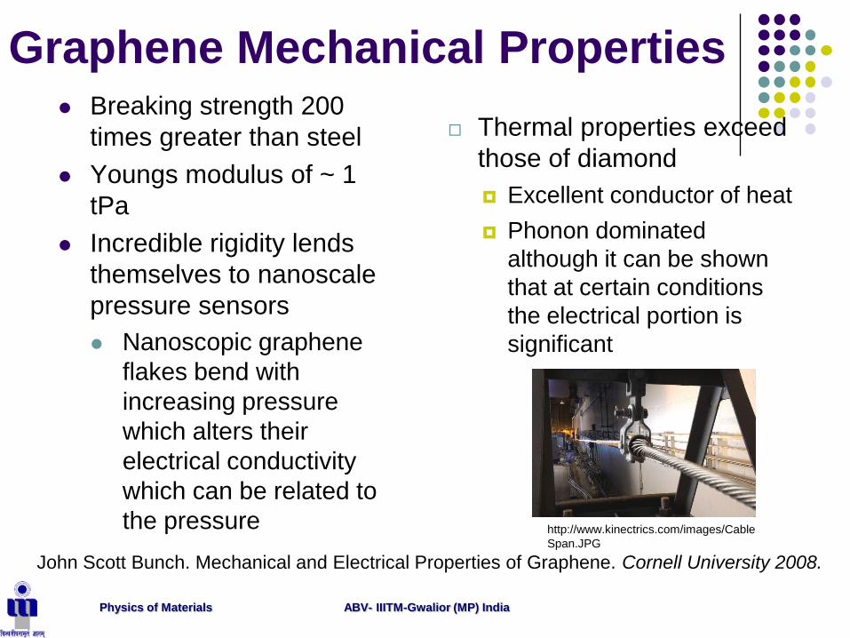
Thermal properties exceed
those of diamond
Excellent conductor of heat
Phonon dominated
although it can be shown
that at certain conditions
the electrical portion is
significant
ABV- IIITM-Gwalior (MP) IndiaPhysics of Materials
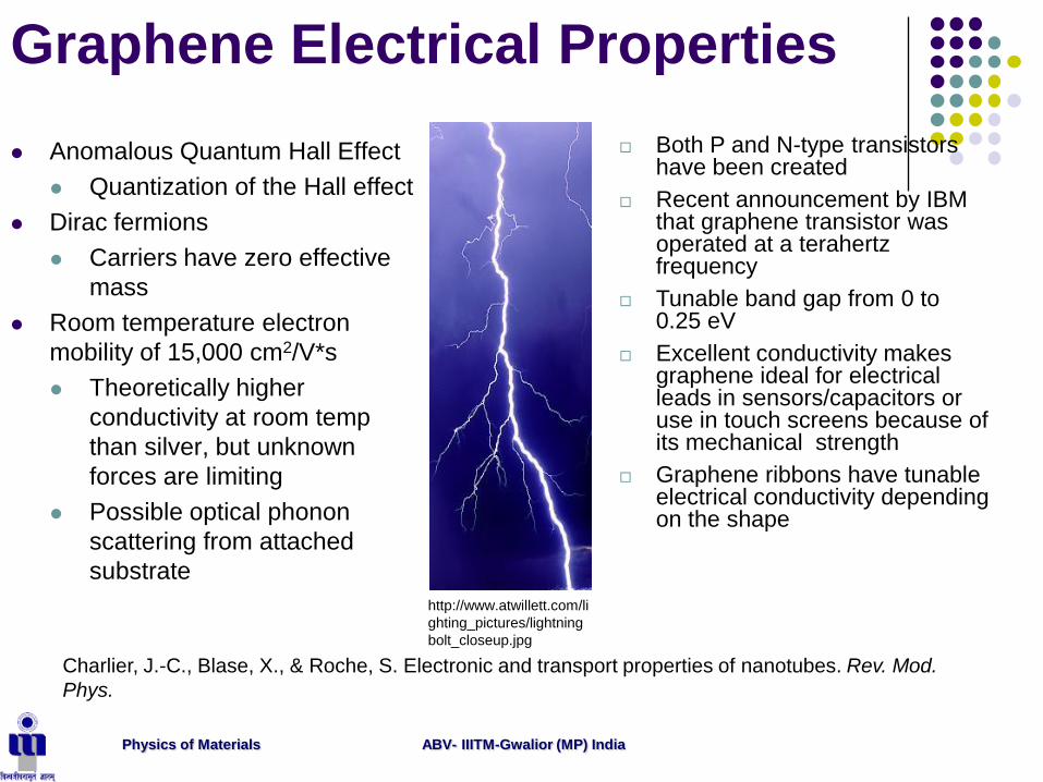
Graphene Electrical Properties
Anomalous Quantum Hall Effect
Quantization of the Hall effect
Dirac fermions
Carriers have zero effective
mass
Room temperature electron
mobility of 15,000 cm2/V*s
Theoretically higher
conductivity at room temp
than silver, but unknown
forces are limiting
Possible optical phonon
scattering from attached
substrate
Charlier, J.-C., Blase, X., & Roche, S. Electronic and transport properties of nanotubes. Rev. Mod.
Phys.
http://www.atwillett.com/li
ghting_pictures/lightning
bolt_closeup.jpg
Both P and N-type transistors have been created
Recent announcement by IBM that graphene transistor was operated at a terahertz frequency
Tunable band gap from 0 to 0.25 eV
Excellent conductivity makes graphene ideal for electrical leads in sensors/capacitors or use in touch screens because of its mechanical strength
Graphene ribbons have tunable electrical conductivity depending on the shape

ABV- IIITM-Gwalior (MP) IndiaPhysics of Materials
Electrical Component: Transistor
A transistor's operation speed depends on the size of the
device — smaller devices can run faster — and the
speed at which electrons travel in it. This size
dependence has been one of the major driving forces for
making ever smaller silicon transistors.
The Consortium of International Semiconductor
Companies in its 2001 International Technology
Roadmap for Semiconductors projected that transistors
have to be smaller than 9 nanometers by 2016 in order
to continue the performance trend.
Charlier, J.-C., Blase, X., & Roche, S. Electronic and transport properties of nanotubes. Rev. Mod.
Phys.

ABV- IIITM-Gwalior (MP) IndiaPhysics of Materials
Carbon vs. Silicon
Figure (a) is Intel’s 45 nm
silicon transistor which uses
a Hafniun based dielectric.
Figure (b) is a wafer of the
45 nm transistors
photographed with a dime.
The processors incorporate
410 million transistors for
each dual core chip, and
820 million for each quad
core chip.
http://www.intel.com/pressroom/kits/45nm/photos.htm.

ABV- IIITM-Gwalior (MP) IndiaPhysics of Materials
Carbon vs. Silicon
Graphene could offer a way forward. As well as being
extremely thin and a semiconductor, electrons move
through graphene at extremely high speeds.
http://mayang.com/textures/Manmade/images/Plastic
s%20and%20Related/electronic_circuit_board_91310
73.JPG
Geim, A. K. & Novoselov, K. S. The rise of graphene. Nature Mater.
The cutting edge of silicon-based
transistors is at 32 nanometers.
Graphene has the potential to fabricate transistors only a few
atoms across. British researchers have unveiled the world’s
smallest transistor, which measures one atom thick and ten
atoms across. This is in the sub-10 nanometer range

ABV- IIITM-Gwalior (MP) IndiaPhysics of Materials
Performance Characteristics for
Carbon-Based TransistorAmbipolar transfer characteristics [current versus gate voltage]: drain bias
increases from –0.1 V to –1.1 V in –0.2 V steps. Red line represents -0.1 V
and the pink line is -1.1 V. Step size is -0.2 V
Left Inset: Schematic
of the band structure
of a Schottky barrier
semiconducting
carbon nanotube in a
field effect transistor
under negative gate
bias. Holes are
injected from the
source [S].
Right Inset:
Schematic of the
band structure of a
Schottky barrier
semiconducting
carbon nanotube in a
field effect transistor
under positive gate
bias. Electrons are
injected from the
drain [D].
Anantram, M. P. & Leonard, F. Physics of carbon nanotube electronic devices. Rep. Prog. Phys.

ABV- IIITM-Gwalior (MP) IndiaPhysics of Materials
Two-dimensional nanomaterials
Two of the dimensions are not confined to the
nanoscale.
2-D nanomaterials exhibit plate-like shapes.
Two-dimensional nanomaterials include
nanofilms,
nanolayers, and
nanocoatings
2-D nanomaterials can be:
Amorphous or crystalline
Made up of various chemical compositions
Used as a single layer or as multilayer structures
Deposited on a substrate
Integrated in a surrounding matrix material
Metallic, ceramic, or polymeric

ABV- IIITM-Gwalior (MP) IndiaPhysics of Materials
2D-Nanostructure
Grpahene Sheet (0-Gap semiconductor)
Boron Nitride Sheet (~4.8eV)
Silicene
Germenene
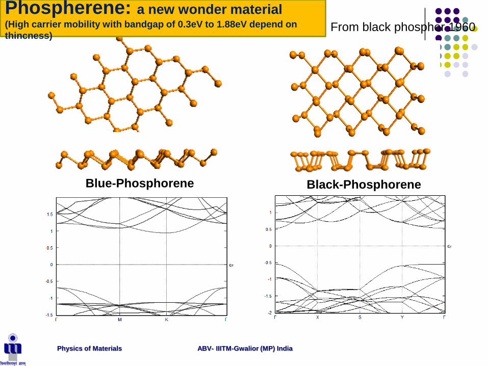
Phospherene
1)Black Phospherene : single layer (Direct Band-Gap) (~1.88eV)
On increasing layers it goes upto 0.3eV (2014)
2)Blue Phospherene (Indirect Band-Gap) (~2eV) 2015
(displacement of some atoms from crystal phospherene blue
phospherene)
Arsenene (Theoretically simulated but experimentally not verified)
Antimonene (Theoretically simulated but experimentally not verified)
Borophene (Theoretically simulated but experimentally not verified)
Flattened
Buckled/ Puckered
sp2
sp3
Buckled
ABV- IIITM-Gwalior (MP) IndiaPhysics of Materials
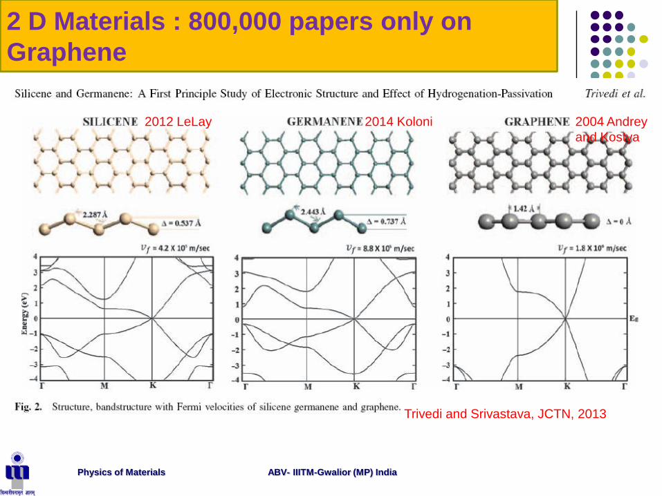
Trivedi and Srivastava, JCTN, 2013
2 D Materials : 800,000 papers only on
Graphene
2004 Andrey
and Kostya
2012 LeLay 2014 Koloni

ABV- IIITM-Gwalior (MP) IndiaPhysics of Materials
Graphene Boron-Nitride
ABV- IIITM-Gwalior (MP) IndiaPhysics of Materials
Blue-Phosphorene Black-Phosphorene
Phospherene: a new wonder material(High carrier mobility with bandgap of 0.3eV to 1.88eV depend on
thincness)From black phosphor 1960

ABV- IIITM-Gwalior (MP) IndiaPhysics of Materials
Arsenene and AntimoneneTheoretically proposed
C. Kamal and M. Ezawa, Phys. Rev. B, 91, 085423,
2015
Z. Zhang, J. Xie, D. Yang, Y. Wang, M. Siand ,D.
Xue,Appl. Phys. Express, 8, 055201, 2015
AntimoneneArsenene