
Physics 116A Notes Fall 2004 - Department of...
13
Physics 116A Notes Fall 2004 David E. Pellett Draft v.0.9 • Notes Copyright 2004 David E. Pellett unless stated otherwise. • References: – Text for course: Fundamentals of Electrical Engineering, second edition, by Leonard S. Bobrow, published by Oxford University Press (1996) – Others as noted 1
Transcript of Physics 116A Notes Fall 2004 - Department of...

Physics 116A NotesFall 2004
David E. Pellett
Draft v.0.9
• Notes Copyright 2004 David E. Pellett unless stated otherwise.
• References:
– Text for course:Fundamentals of Electrical Engineering, second edition, by LeonardS. Bobrow, published by Oxford University Press (1996)
– Others as noted
1
Physics 116A, BJT Basics: Outline
• Bipolar Junction Transistor (BJT) fabrication (diagram)
• BJT regions of operation
• BJT active region behavior and Ebers-Moll model
• Overview of simple BJT amplifiers
• Q-point analysis
• Small signal AC analysis
• A simple small signal AC BJT model
2
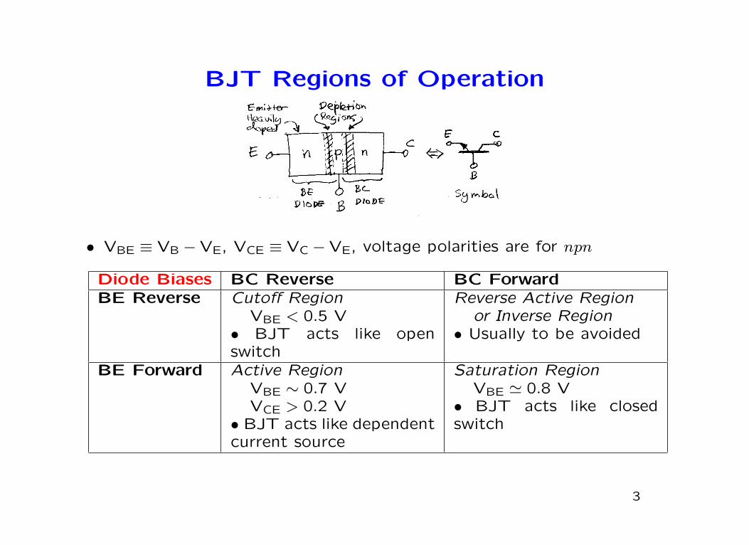
BJT Regions of Operation
• VBE ≡ VB −VE, VCE ≡ VC −VE, voltage polarities are for npn
Diode Biases BC Reverse BC ForwardBE Reverse Cutoff Region
VBE < 0.5 V• BJT acts like openswitch
Reverse Active Regionor Inverse Region
• Usually to be avoided
BE Forward Active RegionVBE ∼ 0.7 VVCE > 0.2 V
• BJT acts like dependentcurrent source
Saturation RegionVBE ' 0.8 V
• BJT acts like closedswitch
3
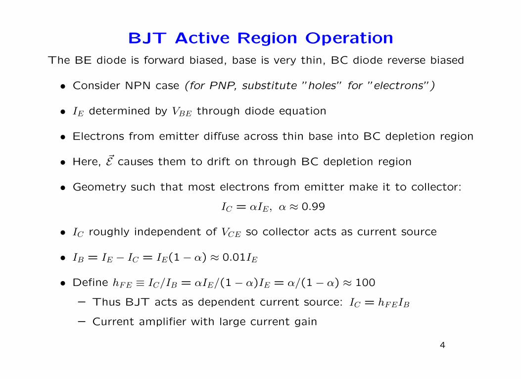
BJT Active Region OperationThe BE diode is forward biased, base is very thin, BC diode reverse biased
• Consider NPN case (for PNP, substitute ”holes” for ”electrons”)
• IE determined by VBE through diode equation
• Electrons from emitter diffuse across thin base into BC depletion region
• Here, ~E causes them to drift on through BC depletion region
• Geometry such that most electrons from emitter make it to collector:
IC = αIE, α ≈ 0.99
• IC roughly independent of VCE so collector acts as current source
• IB = IE − IC = IE(1− α) ≈ 0.01IE
• Define hFE ≡ IC/IB = αIE/(1− α)IE = α/(1− α) ≈ 100
– Thus BJT acts as dependent current source: IC = hFEIB
– Current amplifier with large current gain
4
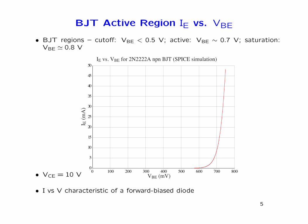
BJT Active Region IE vs. VBE
• BJT regions – cutoff: VBE < 0.5 V; active: VBE ∼ 0.7 V; saturation:VBE ' 0.8 V
0
5
10
15
20
25
30
35
40
45
50IE vs. VBE for 2N2222A npn BJT (SPICE simulation)
VBE (mV)
I E (m
A)
0 100 200 300 400 500 600 700 800• VCE = 10 V
• I vs V characteristic of a forward-biased diode
5
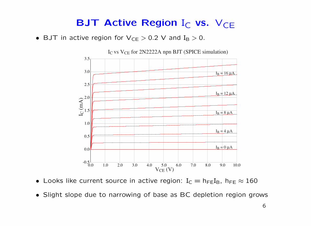
BJT Active Region IC vs. VCE
• BJT in active region for VCE > 0.2 V and IB > 0.
0.0 1.0 2.0 3.0 4.0 5.0 6.0 7.0 8.0 9.0 10.0-0.5
0.0
0.5
1.0
1.5
2.0
2.5
3.0
3.5IC vs VCE for 2N2222A npn BJT (SPICE simulation)
I C (m
A)
VCE (V)
IB = 8 µA
IB = 0 µA
IB = 4 µA
IB = 12 µA
IB = 16 µA
• Looks like current source in active region: IC = hFEIB, hFE ≈ 160
• Slight slope due to narrowing of base as BC depletion region grows
6
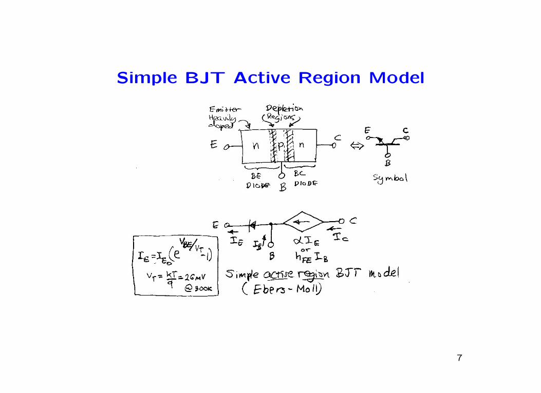
Simple BJT Active Region Model
7
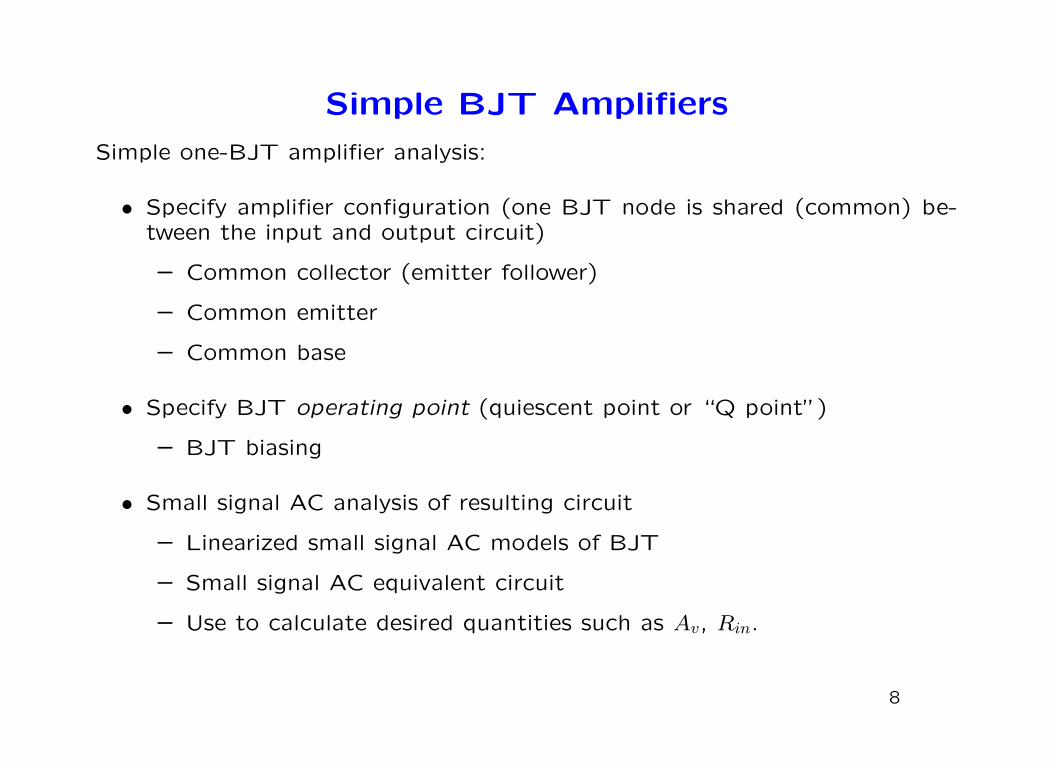
Simple BJT Amplifiers
Simple one-BJT amplifier analysis:
• Specify amplifier configuration (one BJT node is shared (common) be-tween the input and output circuit)
– Common collector (emitter follower)
– Common emitter
– Common base
• Specify BJT operating point (quiescent point or “Q point”)
– BJT biasing
• Small signal AC analysis of resulting circuit
– Linearized small signal AC models of BJT
– Small signal AC equivalent circuit
– Use to calculate desired quantities such as Av, Rin.
8
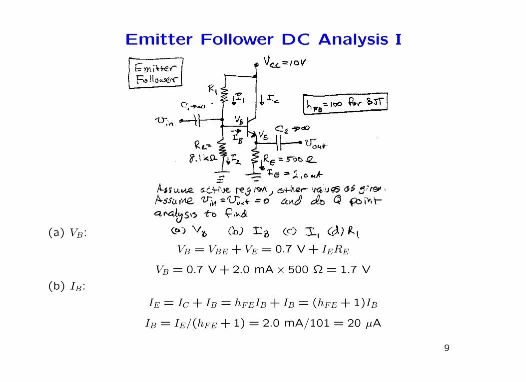
Emitter Follower DC Analysis I
(a) VB:
VB = VBE + VE = 0.7 V + IERE
VB = 0.7 V + 2.0 mA× 500 Ω = 1.7 V
(b) IB:
IE = IC + IB = hFEIB + IB = (hFE + 1)IB
IB = IE/(hFE + 1) = 2.0 mA/101 = 20 µA
9
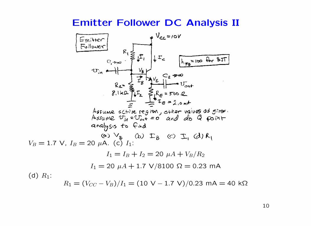
Emitter Follower DC Analysis II
VB = 1.7 V, IB = 20 µA. (c) I1:
I1 = IB + I2 = 20 µA + VB/R2
I1 = 20 µA + 1.7 V/8100 Ω = 0.23 mA
(d) R1:R1 = (VCC − VB)/I1 = (10 V − 1.7 V)/0.23 mA = 40 kΩ
10
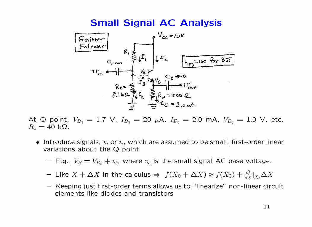
Small Signal AC Analysis
At Q point, VBQ= 1.7 V, IBQ
= 20 µA, IEQ= 2.0 mA, VEQ
= 1.0 V, etc.R1 = 40 kΩ.
• Introduce signals, vi or ii, which are assumed to be small, first-order linearvariations about the Q point
– E.g., VB = VBQ+ vb, where vb is the small signal AC base voltage.
– Like X + ∆X in the calculus ⇒ f(X0 + ∆X) ≈ f(X0) + dfdX|X0
∆X
– Keeping just first-order terms allows us to “linearize” non-linear circuitelements like diodes and transistors
11
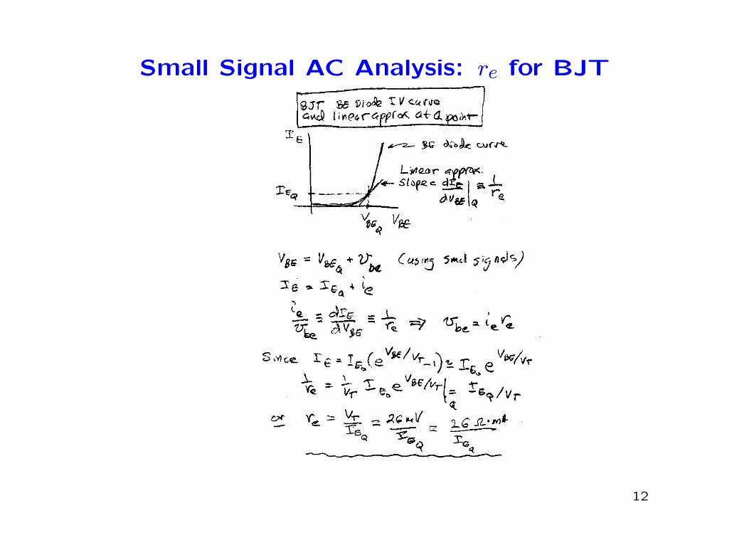
Small Signal AC Analysis: re for BJT
12
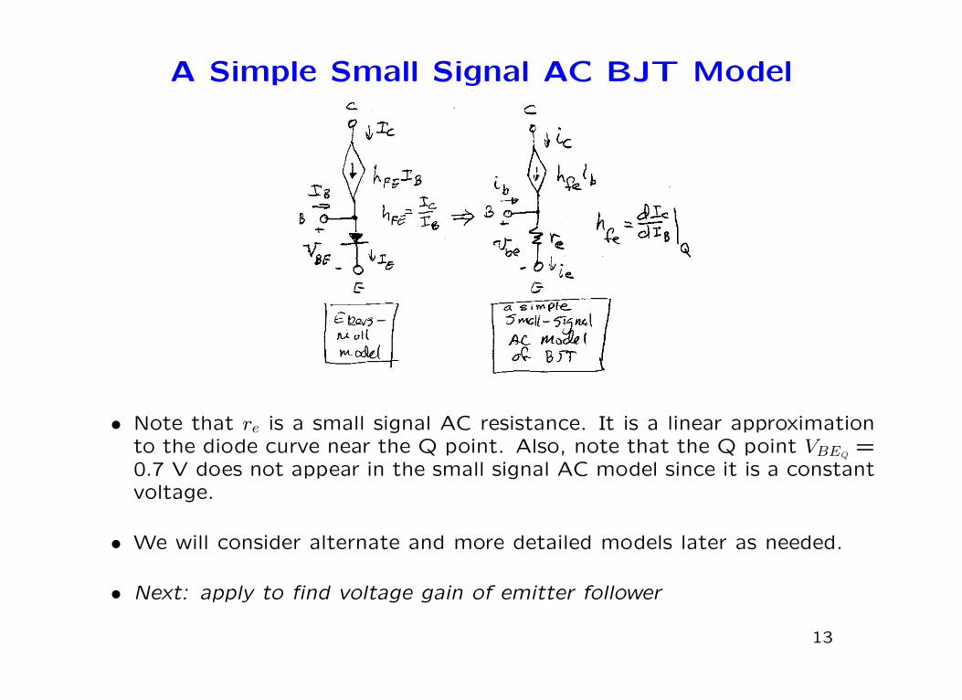
A Simple Small Signal AC BJT Model
• Note that re is a small signal AC resistance. It is a linear approximationto the diode curve near the Q point. Also, note that the Q point VBEQ
=0.7 V does not appear in the small signal AC model since it is a constantvoltage.
• We will consider alternate and more detailed models later as needed.
• Next: apply to find voltage gain of emitter follower
13


