Physical Unclonable Functions based on Temperature Compensated Ring Oscillators · 2016-09-14 ·...
15
Physical Unclonable Functions based on Temperature Compensated Ring Oscillators Sha Tao and Elena Dubrova KTH Royal Institute of Technology Kistag˚ angen 16, 164 40 Stockholm, Sweden Abstract. Physical unclonable functions (PUFs) are promising hard- ware security primitives suitable for low-cost cryptographic applications. Ring oscillator (RO) PUF is a well-received silicon PUF solution due to its ease of implementation and entropy evaluation. However, the re- sponses of RO-PUFs are susceptible to environmental changes, in par- ticular, to temperature variations. Additionally, a conventional RO-PUF implementation is usually more power-hungry than other PUF alter- natives. This paper explores circuit-level techniques to design low-power RO-PUFs with enhanced thermal stability. We introduce a power-efficient approach based on a phase/frequency detector (PFD) to perform pair- wise comparisons of ROs. We also propose a temperature compensated bulk-controlled oscillator and investigate its feasibility and usage in PFD- based RO-PUFs. Evaluation results demonstrate that the proposed tech- niques can effectively reduce the thermally induced errors in PUF re- sponses while imposing a very low power overhead. Keywords: Physical unclonable function (PUF), delay-based PUF, RO- PUF, temperature variation, hardware security, device authentication. 1 Introduction Physical unclonable functions (PUFs) which extract inherent randomness in physical devices have recently emerged as a light-weight cryptographic prim- itive. Over the past decade, PUFs have found their usage in many practical applications such as device identification, authentication, secret key generation and storage [1, 2]. Among different solutions, the most popular and low-cost PUFs are based on uncontrollable and unpredictable process variations during silicon manufacturing. From an implementation perspective, most existing sili- con PUFs can be widely divided into two categories: (1) delay-based, including arbiter PUFs [1] and ring oscillator (RO) PUFs [2], (2) bistable element-based, such as SRAM-PUFs [3] and bistable ring PUFs [4]. An extensive characteri- zation and comparative study of different silicon PUFs fabricated on the same CMOS technology can be found in [5].
Transcript of Physical Unclonable Functions based on Temperature Compensated Ring Oscillators · 2016-09-14 ·...

Physical Unclonable Functions based onTemperature Compensated Ring Oscillators
Sha Tao and Elena Dubrova
KTH Royal Institute of TechnologyKistag̊angen 16, 164 40 Stockholm, Sweden
Abstract. Physical unclonable functions (PUFs) are promising hard-ware security primitives suitable for low-cost cryptographic applications.Ring oscillator (RO) PUF is a well-received silicon PUF solution dueto its ease of implementation and entropy evaluation. However, the re-sponses of RO-PUFs are susceptible to environmental changes, in par-ticular, to temperature variations. Additionally, a conventional RO-PUFimplementation is usually more power-hungry than other PUF alter-natives. This paper explores circuit-level techniques to design low-powerRO-PUFs with enhanced thermal stability. We introduce a power-efficientapproach based on a phase/frequency detector (PFD) to perform pair-wise comparisons of ROs. We also propose a temperature compensatedbulk-controlled oscillator and investigate its feasibility and usage in PFD-based RO-PUFs. Evaluation results demonstrate that the proposed tech-niques can effectively reduce the thermally induced errors in PUF re-sponses while imposing a very low power overhead.
Keywords: Physical unclonable function (PUF), delay-based PUF, RO-PUF, temperature variation, hardware security, device authentication.
1 Introduction
Physical unclonable functions (PUFs) which extract inherent randomness inphysical devices have recently emerged as a light-weight cryptographic prim-itive. Over the past decade, PUFs have found their usage in many practicalapplications such as device identification, authentication, secret key generationand storage [1, 2]. Among different solutions, the most popular and low-costPUFs are based on uncontrollable and unpredictable process variations duringsilicon manufacturing. From an implementation perspective, most existing sili-con PUFs can be widely divided into two categories: (1) delay-based, includingarbiter PUFs [1] and ring oscillator (RO) PUFs [2], (2) bistable element-based,such as SRAM-PUFs [3] and bistable ring PUFs [4]. An extensive characteri-zation and comparative study of different silicon PUFs fabricated on the sameCMOS technology can be found in [5].

2
1.1 Prior Related Works
Among many PUF variants, the PUF structure based on comparing the fre-quency difference of ring oscillator pairs, called RO-PUF, has become a popularsolution due to its ease of implementation and entropy evaluation [2]. For reliableidentification and authentication, PUF designs are expected to provide stableresponses under varying operating conditions. However, the frequency of ROschanges with varying environment. In addition, the rate of change in frequencycan also vary for different ROs. These, in turn, lead to unstable responses.
In this subsection, we review existing reliability enhancement methods ap-plied specifically to RO-PUFs. Error correction codes (ECCs) have been tradi-tionally applied to RO-PUFs to produce error-free responses [6]. However, ECCsusually impose high overhead, which also scales up quickly with the increasednumber of error correction bits [7]. Alternatively, various architectural and cir-cuit level techniques have been proposed in the literature to improve reliabilityof RO-PUFs.
From an architectural perspective, the first RO-PUF design [2] employs a 1-out-of-N masking scheme that selects only those pairs with frequency differencessufficiently large to overwhelm environmental noise. In [8], a temperature-awarecooperative RO-PUF is proposed, which defines a bit-generation rule so as toconvert unreliable bits into reliable ones. A more hardware-efficient approach issuggested in [9], where a feedback-based supply control scheme is used to varysupply voltage according to operating temperature. Another approach, intro-duced in [10], improves the reliability of RO-PUFs against temperature variationthrough applying multiple supply voltages on different inverters in each RO.
From a circuit perspective, one way of increasing the stability of RO-PUFsagainst supply variation is to operate the transistors with a forward body bias[11]. In [12], two methods for reducing temperature sensitivity of delay basedPUFs are proposed. The first finds an optimum power supply under which tem-perature effects are minimized. The second uses negative temperature coefficientresistance to compensate for temperature effects of inverters. Both methods areapplied to a conventional RO-PUF and a phase differential RO-PUF proposedin [13]. Most recently, a hybrid RO-PUF is proposed [14], which uses the positivetemperature coefficient of current starved inverters to offset the response instabil-ity due to the negative temperature coefficient of regular inverters. Furthermore,in [15], the impact of aging effect is addressed, and the first aging-resistant PUFdesign is presented.
1.2 Contributions and Organization
In this work, we aim to counteract the effect of temperature-induced frequencyerrors in ring oscillators, which is considered to be a major problem that can no-tably degrade the reliability of a RO-PUF. Our contributions can be summarizedas follows: (1) We investigate and compare two circuit-level techniques for real-izing temperature compensated ROs, namely, bulk-controlled oscillator (BCO)and current-starved voltage-controlled oscillator (CSVCO). (2) Inspired by the

3
MU
XM
UX
n random
challenges
C0
C1
Cn
Phase/Frequency
Detector (PFD)
n output
responsesEN
NAND
NAND
O1
O2
N Temperature Compensated Ring Oscillators
BUF BUF
BUF BUF
NAND BUF BUF
ON
10-stage Inverter Chain
10-stage Inverter Chain
10-stage Inverter Chain
D Q
Clk
Rst Q
D Q
Clk
Rst Q
UP
DN
IN1
IN2
Charge
Pump
OUT
Po
st-
Pro
ce
ss
ing
Fig. 1. Block diagram of the proposed temperature aware PUF.
topology in [13], we propose an alternative method based on a phase/frequencydetector (PFD) to extract difference in RO pairs for reliable PUF response gen-eration. (3) We demonstrate that the proposed design is effective for reducingthe error-rate in PUF responses over temperatures and shows satisfying resis-tance to supply ripples while featuring a low power overhead comparable to thestate-of-the-art designs.
The rest of this paper is organized as follows. In Section 2, we describe theproposed PFD-based PUF and elaborate the design and analysis of its circuitblocks. The experimental methodology and PUF evaluation results are presentedand discussed in Section 3. Section 4 concludes the paper and .
2 Proposed PUF Design
The concept of the proposed temperature aware PUF is illustrated in Fig. 1.To generate a response, one pair of temperature compensated ROs is enabledand selected by two multiplexers that are controlled by a random challenge.Unlike conventional RO-PUFs that use power- and time-consuming countersand comparators to compare oscillating frequencies, the proposed PUF employsa phase/frequency detector (PFD) followed by a charge pump (CP) which arewidely used in phase-locked loops (PLLs) for clock generation [16].
2.1 RO-PUFs based on Phase/Frequency Detector
Fig. 2 shows the schematic and timing diagram of the designed PFD and CP. ThePFD, consisting of two D flip-flops (DFF), compares the leading edges of twosignals, ‘IN1’ and ‘IN2’, coming from two selected ROs. The outputs of PFD,‘UP’ and ‘DN’, depend on both phase and frequency differences between twoinput signals. For instance, Fig. 2 (b) illustrates the case of ‘IN1’ leading ‘IN2’:‘UP’ goes high when there is a rising edge on ‘IN1’ and is reset by a rising edgeon ‘IN2’. The transition is similar for the case shown in Fig. 2 (c) where ‘IN2’is faster. The ‘UP’ and ‘DN’ signals control the CP consisting of two switchedcurrent sources: when ‘UP’ is high and ‘DN’ is low, the load capacitor is chargedthus raising the voltage of ‘OUT’; when ‘DN’ is high and ‘UP’ is low, the load

4
VDD
Phase/Frequency Detector (PFD)
IN1
IN2
VDD
VDD
VDD VDD
VDD
UP
DN
VDD VDD
Charge Pump (CP)
VDD
OUT
(a)
IN1
IN2
UP
DN
OUT
IN1
IN2
UP
DN
OUT
tt
(b)
IN1
IN2
UP
DN
OUT
IN1
IN2
UP
DN
OUT
tt
(c)
Fig. 2. PFD and CP: (a) circuit schematics, (b) timing diagram when fIN1>fIN2, and(c) timing diagram when fIN1<fIN2.
capacitor is discharged thus reducing the voltage of ‘OUT’; when both ‘UP’ and‘DN’ are low, both switches are off and thus the voltage of ‘OUT’ remains. Bythe end of each enable period, ‘OUT’ can be captured by a logic analyzer inpractice with thresholds VTH = VTL = VDD/2.
Compared to the phase differential RO-PUF [13] that uses a latched com-parator to sense an instant output voltage difference of two ROs at end of anenable signal ‘EN’, our PFD-based approach not only consumes less power, butalso provides better comparison accuracy, since the phase/frequency differenceof two ROs are accumulated for a period and thus gets “amplified” rather thanbeing decided at once. Moreover, this PFD-based approach has no concern ofreliability issue induced by the jitter effect of the enable signal ‘EN’. On theother hand, in this approach, the result is not directly varied by the duration of‘EN’. Therefore, we cannot apply the area-efficient method in [13], where ‘EN’with various pulse widths are used as challenges feeding into the same RO pair.
Like in conventional RO-PUFs, to generate n output responses with maxi-mum entropy, the total number of ROs, N, needs to satisfy: log2(N !) ≥ n. Forinstance, to generate n = 128 independent bits, N = 36 ring oscillators arerequired. We can use the redundant log2(36!) − 128 ≈ 10 bits to perform anoptional data screening (DS) at post-processing. The DS eliminates 10 out of138 output responses while the candidates are determined according to the de-tected phase/frequency difference. We remove the responses generated by 10 RO

5
VDD
VCtrlVCtrl
VDD VDD VDD
VDD
10-stage Current Starved Inverters
Buffers
VDD
VBp
VBn
VDD
NAND
EN
BIAS
O
VDD
MBN1 MBN2 MBN10
MBP1 MBP2 MBP10
(a)
VBulkVBulkVDD VDD VDD
VDD
O
10-stage Bulk Controlled InvertersBuffers
VDD
VDD
NAND
EN
VDD
MP1 MP2 MP10
(b)
Fig. 3. (a) Schematic of (a) Current-starved voltage-controlled oscillator (CSVCO) and(b) bulk-controlled oscillator (BCO).
pairs with the minimum absolute value of ‘OUT’, which can be recorded by anoscilloscope in practice.
2.2 Temperature Compensated Bulk-Controlled Oscillators
Voltage controlled oscillator (VCO) is the core building block of PLL circuits.VCOs which employ current starvation to control their output frequencies arecalled current-starved VCO (CSVCO) [17]. However, the relationship betweenoutput frequency and input control voltage is very non-linear in CSVCOs. Alter-natively, controlling the frequency through tuning the bulk voltage of transistorscan alleviate the linearity issue [18]. In this subsection, we introduce a bulk-controlled oscillator (BCO) with dynamic temperature correction to be used inthe proposed PUF. We investigate its hardware overhead and its feasibility inminimizing frequency errors due to environmental changes. We also demonstratethe advantages of this BCO based approach over its CSVCO based counterpart.
Fig. 3 (a) shows the schematic of a CSVCO consisting of a 10-stage CS in-verter chain whose delay is controlled by VCtrl, buffer inverters whose delays are

6
380 390 400 410 420 430VCtrl [mV]
0.98
0.99
1
1.01
1.02
1.03
Fre
quen
cy [G
Hz]
100806040200
Temperature [oC]
0.98
0.99
1.00
1.01
1.02
1.03
Fre
quen
cy [G
Hz]
(a) (b)
Fig. 4. Frequency of CSVCO vs. (a) VCtrl and (b) temperature.
-100-50050100150V
BS [mV]
1.06
1.08
1.1
1.12
1.14
1.16
Fre
quen
cy [G
Hz]
0 20 40 60 80 100
Temperature [oC]
1.06
1.08
1.1
1.12
1.14
1.16
Fre
quen
cy [G
Hz]
(a) (b)
Fig. 5. Frequency of BCO vs. (a) VBS and (b) temperature.
made negligible compared to the CS inverter chain, and a NAND gate to enableor disable the RO. It has been shown in [19] that using CS inverters in delaybased PUF circuits is beneficial, as they can increase the standard deviationof delay compared to regular inverters. For ROs, this advantage remains. Thecontrol voltage VCtrl modulates the on-resistance of current source transistorsMBN1−BN10 and MBP1−BP10 through a BIAS circuit. These variable resistancesregulate peak current available at each inverter stage and thus vary its prop-agation delay which, in turn, controls the frequency of RO. The frequency ofCSVCO, fOSC , is proportional to (VCtrl − Vth)2 when the current source tran-sistors are in saturation [17]. Fig. 4 (a) illustrates the simulation results whenVDD is 0.9V, showing that the fOSC increases with increasing VCtrl in a non-linear way. To maximize the mismatch, the core inverters are biased in the weakinversion region. In this region, with the increase of temperature, the decreaseof threshold Vth(T ) dominates the decrease of mobility µ(T ) [14]. Additionally,the current at each stage is proportional to µ(T ) and inversely related to Vth(T ).Thus, fOSC of the CSVCO increases with the increase of temperature. This isconfirmed by the simulation results shown in Fig. 4 (b).
Alternatively, we can solve the linearity issue in the CSVCO by controllingthe bulk potential of inverters. Fig. 3 (b) shows the schematic of a BCO, whichreplaces the CS inverters in Fig. 3 (a) with regular inverters. The bulk of all

7
PMOS1, MP1−P10, is connected to a control voltage VBulk. When PMOS is bi-ased to a potential other than VDD, its threshold voltage is proportional toγ(√
2φf − VBS) [18], where γ is a process constant and φf is the surface po-tential of the PMOS. Therefore, when VBS increases, Vth reduces, leading to anincreased current at each stage and, consequently, an increase of fOSC . This isconfirmed by the simulation results illustrated in Fig. 5 (a) (VDD is 0.9V). Itshows a linear relationship between the frequency of BCO and the bulk-to-sourcepotential VBS although its tuning range is smaller than the CSVCO case. In-verters in the BCO operate in the saturation region, where with the increase oftemperature, the decrease of mobility µ(T ) dominates the decrease of thresholdVth(T ) [12]. Thus, when temperature is increased, the overall current is reducedleading to a decrease in frequency. This is confirmed by the simulation resultsshown in Fig. 5 (b).
From the above analysis, we can see that the thermal effect of CSVCO andBCO can be compensated by adjusting their control voltages VCtrl and VBulk,respectively. In Fig. 6, we compare the resulting frequency errors with respect tothe reference frequency at 25◦C of two temperature compensated ROs2. Com-pared to CSVCO, the BCO based approach is much more effective in reducingtemperature sensitivity: the frequency error is limited to less than 1%. Fig. 7plots the distribution of relative frequency deviation due to process variationobtained from 1000 instances of each RO, indicating that the “desired” fre-quency deviation among different PUF instances is larger than the “undesired”frequency error due to temperature changes. The averaged current consumedby BCO and CSVCO is 14.55µA and 21.34µA, respectively3. Fig. 8 shows thelayouts of two ROs, implemented manually in Cadence Virtuoso. Thanks to theelimination of 20 chunky current source transistors used for current starvation,BCO is much more area-efficient than CSVCO. The chip area of the BCO andCSVCO is 39.27µm2 and 613.74µm2, respectively.
Fig. 9 illustrates an implementation example of the voltage references4,5 forthe proposed BCO and CSVCO, which are derived from a 1.2V external ref-erence VDD,ext. Fig. 10 shows their simulation results. Both control voltagesare generated by a simple NMOS voltage divider, whose output VBulk or VCtrl
has a negative temperature coefficient (TC) and thus decreases with increasing
1 We control the bulk of PMOS not NMOS due to the following reasons: (1) Biasingthe bulk of NMOS requires a triple well CMOS process while biasing the bulk ofPMOS can be applied to any standard CMOS process. (2) Creating a bias voltagearound VDD for PMOS is more straight forward and easier than creating a biasvoltage around GND for NMOS.
2 For fair comparison, both ROs oscillate at a similar nominal frequency. Thus, BCOis power by 0.9V and CSVCO uses a higher supply of 1V.
3 Note that essentially the CSVCO can have a much less current consumption with amuch lower fOSC when biased towards deep weak-inversion.
4 In addition to regular transistors (RVT), high threshold voltage (HVT) NMOS tran-sistors are used in the design to reduce static current consumption.
5 Note that these voltage references can be shared by all ROs in the PUF IC in orderto minimize hardware overhead.

8
0 20 40 60 80 100
Temperature [oC]
-0.4
-0.1
0.2
0.5
0.8
Fre
quen
cy e
rror
[%]
(a)
0 20 40 60 80 100
Temperature [oC]
-3
-1.5
0
1.5
3
Fre
quen
cy e
rror
[%]
(b)
Fig. 6. Frequency error (compared to the reference at 25◦C) after temperature com-pensation: (a) BCO and (b) CSVCO.
-30 -20 -10 0 10 20 30Frequency deviation [%]
0
50
100
150
200
His
togr
am c
ount < = 7.06%
(a)
-30 -20 -10 0 10 20 30Frequency deviation [%]
0
50
100
150
200
His
togr
am c
ount < = 7.22%
(b)
Fig. 7. Histogram of the frequency deviation obtained from 1000 Monte-Carlo simula-tions: (a) BCO and (b) CSVCO.
11.9 um
3.3
um
10-stage bulk controlled inverter chainNAND Buffers
(a)
15
.9 u
m
38.6 um
NANDBuffers
10-stage current-starved voltage controlled inverter chainBIAS
(b)
Fig. 8. Layouts of (a) BCO and (b) CSVCO.

9
VDDVDD
VBulkVBulk
VDD,ext
VDDVDD
22µ
1µ
28µ
1µ
28µ
1µ
2µ
1µ
HVT
NMOS
RVT
PMOS
RVT
NMOS
HVT
NMOS
HVT
NMOS
6µ
1µ
RVT
PMOS
2µ
1µ
1µ
1µ
10µ
0.2µ
VCtrlVCtrl
RVT
NMOS
1.2V
20µ
1µ
10µ
1µ
10µ
1µ
10µ
1µ
20µ
1µ
20µ
1µ
BCOBCO CSVCO CSVCO
RVT: Regular Threshold Voltage
HVT: High Voltage Threshold
VDD,ext VDD,ext
VDD,ext
Fig. 9. Voltage reference generation circuits.
0 20 40 60 80 100
Temperature [oC]
800
850
900
950
1000
Vol
tage
[mV
]
VBulk
for BCO
0 20 40 60 80 100
Temperature [oC]
0.85
0.875
0.9
0.925
0.95
Vol
tage
[V]
VDD
for BCO
0 20 40 60 80 100
Temperature [oC]
350
375
400
425
450
Vol
tage
[mV
]
VCtrl
for CSVCO
0 20 40 60 80 100
Temperature [oC]
0.95
0.975
1
1.025
1.05
Vol
tage
[V]
VDD
for CSVCO
Fig. 10. Temperature dependency of voltage references.
temperature. On the other hand, the supply voltage VDD for both ROs shouldnot be sensitive to temperature changes. As shown in Fig. 9, a voltage dividerconsisting of both PMOS and NMOS is used to generate such a temperature in-sensitive reference6. The basic idea is to use the positive TC of PMOS threshold(−∂Vth,P
∂T > 0) to compensate the negative TC of NMOS threshold (∂Vth,N
∂T < 0),so as to achieve an almost zero TC[17] at the output.
Next, we briefly discuss the impact of supply variation on both ROs. In bothcases, when VDD,ext varies, VDD, VBulk and VCtrl follow the voltage changesaccordingly in the same direction. For instance, when VDD,ext decreases, a dropin both VDD reduces the fOSC of both ROs. For BCO, a drop in VBulk reduces
6 In practice, such a temperature-resistance VDD can be generated by a bandgapvoltage reference, e.g, a low power bandgap presented in [20].

10
the VBS , and thus increases the fOSC according to Fig. 5 (a). For CSVCO, onthe other hand, a drop in VCtrl reduces the current at each CS inverter stage,and thus further decreases the fOSC . Therefore, in comparison with its CSVCOcounterpart, the BCO based approach has another advantage in minimizing thePUF’s sensitivity to supply noise.
3 Evaluation Results
3.1 Methodology
The PUF circuits were designed using a standard 65 nm CMOS technology andsimulated using Cadence Spectre. Matlab was used to perform post-processingand compute performance metrics. The nominal operating condition was at 25◦Cwith VDD = 0.9V for BCO-PUF and VDD = 1V for CSVCO-PUF. To emulatethe characterization of 100 different PUF IC chips, 100 runs of Monte-Carlosimulations were performed. Realistic models provided by a commercial foundrywere used in the simulations. Both process and mismatch options were enabledto account for intra-die and inter-die variations. Such a transistor-level Monte-Carlo simulation based experimental methodology has been adopted in manyPUF literatures, e.g., [11, 3, 7, 12, 13, 9, 19, 4, 15].
3.2 Uniqueness Analysis
We first evaluate the PUF’s uniqueness, U , at the nominal condition, using theaverage inter-chip Hamming Distance (HDinter) of the responses from k different
PUF instances: U = 2k(k−1)
k−1∑i=1
k∑j=i+1
HD(Ri,Rj)n × 100%, where Ri and Rj are
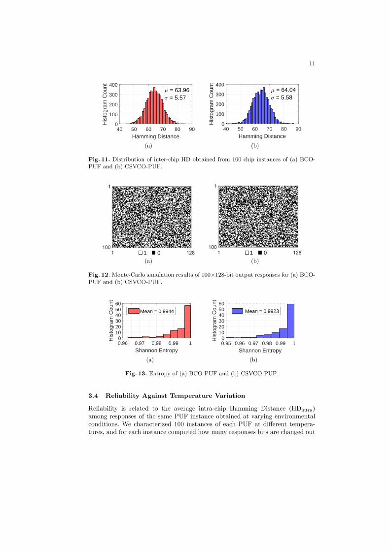
the n-bit responses of instances i and j. Perfect identification of different chipsrequires HDinter = n/2 and U = 50%. For both PUFs, we applied 128 randomchallenges to each of k = 100 instances. So, 100 × 99/2 = 4950 comparisonswere used to compute the HDinter. As shown in Fig. 11, the average HDinter oftwo PUFs are 63.96 and 64.04, corresponding to the uniqueness of 49.97% and50.03%.
3.3 Randomness and Entropy
Randomness measures the proportion of ‘0’s or ‘1’s in PUF responses. Ideally,this proportion should be very close to 50%, since any bias towards ‘0’ or ‘1’make the PUF responses predictable and easier to attack. Fig. 12 (a) and (b)depict output responses from 100 IC instances of BCO-PUF and CSVCO-PUF,characterized at the nominal condition, showing no systematic pattern or notice-able correlation among response bits. Randomness or unpredictability of PUFresponses can also be evaluated by Shannon entropy, H = −p1log2p1 − (1 −p1)log2(1− p1), where p1 is the proportion of ‘1’s in n response bits. Entropy Happroaches the ideal value of 1 when p1 approaches 50%. Fig. 13 shows that theaverage entropy of BCO-PUF and CSVCO-PUF are 0.9944 and 0.9923.
11
40 50 60 70 80 90
Hamming Distance
0
100
200
300
400
His
togr
am C
ount
7 = 63.96< = 5.57
(a)
40 50 60 70 80 90
Hamming Distance
0
100
200
300
400
His
togr
am C
ount
7 = 64.04< = 5.58
(b)
Fig. 11. Distribution of inter-chip HD obtained from 100 chip instances of (a) BCO-PUF and (b) CSVCO-PUF.
1 0
(a)
1 0
(b)
Fig. 12. Monte-Carlo simulation results of 100×128-bit output responses for (a) BCO-PUF and (b) CSVCO-PUF.
0.96 0.97 0.98 0.99 1
Shannon Entropy
0102030405060
His
togr
am C
ount
Mean = 0.9944
(a)
0.95 0.96 0.97 0.98 0.99 1
Shannon Entropy
0102030405060
His
togr
am C
ount
Mean = 0.9923
(b)
Fig. 13. Entropy of (a) BCO-PUF and (b) CSVCO-PUF.
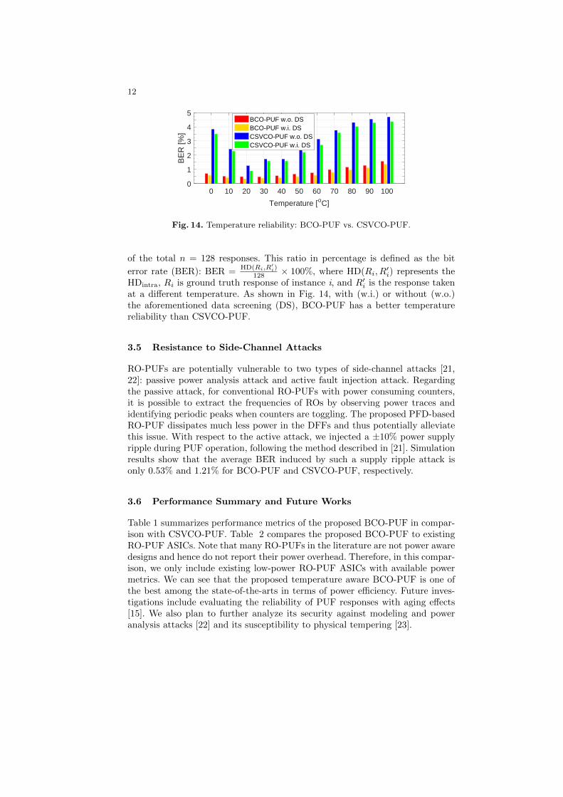
3.4 Reliability Against Temperature Variation
Reliability is related to the average intra-chip Hamming Distance (HDintra)among responses of the same PUF instance obtained at varying environmentalconditions. We characterized 100 instances of each PUF at different tempera-tures, and for each instance computed how many responses bits are changed out
12
0 10 20 30 40 50 60 70 80 90 100
Temperature [oC]
0
1
2
3
4
5
BE
R [%
]
BCO-PUF w.o. DSBCO-PUF w.i. DSCSVCO-PUF w.o. DSCSVCO-PUF w.i. DS
Fig. 14. Temperature reliability: BCO-PUF vs. CSVCO-PUF.
of the total n = 128 responses. This ratio in percentage is defined as the bit
error rate (BER): BER =HD(Ri,R
′i)
128 × 100%, where HD(Ri, R′i) represents the
HDintra, Ri is ground truth response of instance i, and R′i is the response takenat a different temperature. As shown in Fig. 14, with (w.i.) or without (w.o.)the aforementioned data screening (DS), BCO-PUF has a better temperaturereliability than CSVCO-PUF.
3.5 Resistance to Side-Channel Attacks
RO-PUFs are potentially vulnerable to two types of side-channel attacks [21,22]: passive power analysis attack and active fault injection attack. Regardingthe passive attack, for conventional RO-PUFs with power consuming counters,it is possible to extract the frequencies of ROs by observing power traces andidentifying periodic peaks when counters are toggling. The proposed PFD-basedRO-PUF dissipates much less power in the DFFs and thus potentially alleviatethis issue. With respect to the active attack, we injected a ±10% power supplyripple during PUF operation, following the method described in [21]. Simulationresults show that the average BER induced by such a supply ripple attack isonly 0.53% and 1.21% for BCO-PUF and CSVCO-PUF, respectively.
3.6 Performance Summary and Future Works
Table 1 summarizes performance metrics of the proposed BCO-PUF in compar-ison with CSVCO-PUF. Table 2 compares the proposed BCO-PUF to existingRO-PUF ASICs. Note that many RO-PUFs in the literature are not power awaredesigns and hence do not report their power overhead. Therefore, in this compar-ison, we only include existing low-power RO-PUF ASICs with available powermetrics. We can see that the proposed temperature aware BCO-PUF is one ofthe best among the state-of-the-arts in terms of power efficiency. Future inves-tigations include evaluating the reliability of PUF responses with aging effects[15]. We also plan to further analyze its security against modeling and poweranalysis attacks [22] and its susceptibility to physical tempering [23].

13
Table 1. Performance summary of proposed PUFs.
BCO-PUF CSVCO-PUF
Output Throughput 50M bps
Response Size 128 bits
Transistor Count 1106 1934
Power (ROs) 28.7µA × 0.9V 42.2µA × 1V
Power (PFD+CP) 11.6µA × 0.9V 12.7µA × 1V
Average Entropy 0.9944 0.9923
Uniqueness (µ, σ) (49.97%, 5.57%) (50.03%, 5.58%)
Temperature Range 0◦C to 100◦C
BER w.i. DS 0.67% 2.81%
BER w.o. DS 0.82% 3.06%
Supply Fault Attack ±10% supply ripple
Average BER 0.53% 1.21%
Table 2. Comparison to low-power RO-PUF ASICs.
Tech- RO Power
nology Freq. per CRP
[13] Optimized supply RO-PUF* 45nm 2.9GHz 82µW
[13] Negative resistance RO-PUF* 45nm 2.6GHz 98µW
[13] Phase differential RO-PUF+ 45nm – 80µW
[14] Hybrid RO-PUF 65nm 0.32GHz 32.3µW
This work: BCO-PUF 65nm 1.13GHz 36.4µW
* Excluding power consumed by multiplexers and counters.+ Excluding power consumed by sense amplifier.
4 Conclusion
This paper presented effective and efficient approaches for enhancing the reli-ability of RO-PUFs. We introduced a PFD-based alternative to the slow andpower-hungry counter-and-comparator configuration. We also investigated twotemperature-compensated ROs, i.e. BCO and CSVCO, and evaluated their use-fulness in constructing temperature aware PUFs. Both PUF circuits were im-plemented in 65nm CMOS circuit and characterized. Results show that theyachieve low power, high uniqueness, and satisfying randomness. The BCO-PUFdemonstrates superior resistance to environmental variations than its CSVCO-PUF counterpart. In future works, we shall assess the aging effect of the proposedPUFs and perform security analysis.

14
Acknowledgment
This work was supported in part by the research grant No SM14-0016 from theSwedish Foundation for Strategic Research (SSF).
References
1. D. Lim, J. W. Lee, B. Gassend, G. Suh, M. van Dijk, and S. Devadas, “ExtractingKeys from Integrated Circuits,” IEEE Trans. Very Large Scale Integr. Syst., vol.13, no. 10, pp. 1200–1205, 2005.
2. G. E. Suh and S. Devadas, “Physical unclonable functions for device authenticationand secret key generation,” in ACM Des. Autom. Conf. (DAC), 2007, pp. 9–14.
3. A. R. Krishna, S. Narasimhan, X. Wang, and S. Bhunia, “MECCA: A robust low-overhead PUF using embedded memory array, in Cryptogr. Hardw. Embed. Syst.(CHES), 2011, pp. 407–420.
4. Q. Chen, P. Lugli, and U. Rhrmair, “Characterization of the Bistable Ring PUF,”in Des. Autom. Test Eur. Conf. Exhib. (DATE), 2012, pp. 1459-1462.
5. R. Maes, V. Rozic, I. Verbauwhede, P. Koeberl, E. van der Sluis, and V. vander Leest, “Experimental evaluation of Physically Unclonable Functions in 65 nmCMOS,” in Eur. Solid State Circuits Conf. (ESSCIRC), 2012, pp. 486–489.
6. M. Yu and S. Devadas, “Secure and robust error correction for physical unclonablefunctions,” IEEE Des. Test Comput., vol. 27, pp. 4865, 2010.
7. E. I. Vatajelu, G. Di Natale, and Paolo Prinetto, “Towards a Highly Reliable SRAM-based PUFs,” in Des. Autom. Test Eur. Conf. Exhib. (DATE), 2016, pp. 273–276.
8. C. Yin and G. Qu, “Temperature-Aware Cooperative Ring Oscillator PUF,” inIEEE Int. Symp. Hardware-Oriented Secur. Trust (HOST), 2009, pp. 36–42.
9. V. Vivekraja and L. Nazhandali, “Feedback based supply voltage control for tem-perature variation tolerant PUFs,” in Int. Conf. VLSI Des. (VLSID), 2011, pp.214–219.
10. S. Mansouri and E. Dubrova, “Ring oscillator physical unclonable function withmulti level supply voltages,” IEEE Int. Conf. Comput. Des. (ICCD), 2012, pp.520–521
11. V. Vivekraja and L. Nazhandali, “Circuit-Level Techniques for Reliable Physi-cally Uncloneable Functions,” in IEEE Int. Symp. Hardware-Oriented Secur. Trust(HOST), 2009, pp. 30–35.
12. R. Kumar, H. Chandrikakutty, and S. Kundu, “On improving reliability of delaybased Physically Unclonable Functions under temperature variations,” in IEEE Int.Symp. Hardware-Oriented Secur. Trust (HOST), 2011, pp. 142–147.
13. R. Kumar, V. Patil, and S. Kundu, “On Design of Temperature Invariant Phys-ically Unclonable Functions Based on Ring Oscillators,” in IEEE Comput. Soc.Annu. Symp. VLSI (ISVLSI), 2012, pp. 165–170.
14. Y. Cao, L. Zhang, C. Chang, and S. Chen, “A Low-Power Hybrid RO PUF WithImproved Thermal Stability for Lightweight Applications,” IEEE Trans. Comput.Des. Integr. Circuits Syst., vol. 34, no. 7, pp. 1143–1147, 2015.
15. M. Rahman, D. Forte, J. Fahrny, and M. Tehranipoor, “ARO-PUF: An aging-resistant ring oscillator PUF design,” in Des. Autom. Test Eur. Conf. Exhib.(DATE), 2014, pp. 1–6.
16. B. Razavi, Design of Analog CMOS Integrated Circuits. McGraw-Hill, 1st Edition,2002.

15
17. R. J. Baker, CMOS Circuit Design, Layout, and Simulation. Wiley-IEEE Press:New York, 3rd Edition, 2010.
18. U. Wismar, D. Wisland, and P. Andreani, “Linearity of bulk-controlled inverterring VCO in weak and strong inversion,” Analog Integr. Circuits Signal Process.,,vol. 50, no. 1, pp. 59–67, 2007.
19. R. Kumar, V. Patil, and S. Kundu, “Design of Unique and Reliable PhysicallyUnclonable Functions based on Current Starved Inverter Chain,” in IEEE Comput.Soc. Annu. Symp. VLSI (ISVLSI), 2011, pp. 165–170.
20. A. Annema and G. Goksun, “A 0.0025mm2 bandgap voltage reference for 1.1Vsupply in standard 0.16µm CMOS,” in Int. Solid-State Circuits Conf. (ISSCC),2012, pp. 364–366.
21. G. Becker and R. Kumar, “Active and passive side-channel attacks on delay basedPUF designs,” Cryptology ePrint Archive, vol. 287, 2014.
22. X. Xu and W. Burleson, “Hybrid side-channel/machine-learning attacks on PUFs:A new threat?,” in Des. Autom. Test Eur. Conf. Exhib. (DATE), 2014, pp. 1–6.
23. C. Helfmeier, C. Boit, D. Nedospasov, S. Tajik, and J. Seifert, “Physical vulnera-bilities of Physically Unclonable Functions,” in Des. Autom. Test Eur. Conf. Exhib.(DATE), 2014, pp. 1–4.