Physical Structure of CMOS Integrated Circuits
24
Physical Structure of CMOS Integrated Circuits Dae Hyun Kim EECS Washington State University
Transcript of Physical Structure of CMOS Integrated Circuits

Physical Structure of CMOS Integrated Circuits
Dae Hyun Kim
EECS Washington State University

References
• John P. Uyemura, “Introduction to VLSI Circuits and Systems,” 2002. – Chapter 3
• Neil H. Weste and David M. Harris, “CMOS VLSI Design: A Circuits and Systems Perspective,” 2011. – Chapter 1

Goal
• Understand the physical structure of CMOS integrated circuits (ICs)

Logical vs. Physical
• Logical structure
• Physical structure
𝑏𝑏 𝑐𝑐
𝑎𝑎
𝑓𝑓
Source: http://www.vlsi-expert.com/2014/11/cmos-layout-design.html

Integrated Circuit Layers
• Semiconductor – Transistors (active elements)
• Conductor
– Metal (interconnect) • Wire • Via
• Insulator
– Separators

Integrated Circuit Layers
• Silicon substrate, insulator, and two wires (3D view)
• Side view
• Top view
Substrate
Insulator
Metal 1 layer
Substrate

Integrated Circuit Layers
• Two metal layers separated by insulator (side view)
• Top view
Substrate
Metal 1 layer
Metal 2 layer
Insulator
Insulator Via 12 (connecting M1 and M2)
Connected Not connected

Integrated Circuit Layers

Integrated Circuit Layers
• Signal transfer speed is affected by the interconnect resistance and capacitance. – Resistance ↑ => Signal delay ↑ – Capacitance ↑ => Signal delay ↑

Integrated Circuit Layers
• Resistance – 𝑅𝑅 = 𝜌𝜌 𝑙𝑙
𝐴𝐴= 𝜌𝜌
𝑡𝑡∙ 𝑙𝑙𝑤𝑤
= 𝑅𝑅𝑠𝑠 ∙𝑙𝑙𝑤𝑤
• 𝑅𝑅𝑠𝑠: sheet resistance (constant)
• 𝜌𝜌: resistivity (= 1𝜎𝜎, 𝜎𝜎: conductivity)
– Material property (constant) – Unit: Ω ∙ 𝑚𝑚
• 𝑡𝑡: thickess (constant) • 𝑤𝑤: width (variable) • 𝑙𝑙: length (variable)
• Example
– 𝜌𝜌: 17.1𝑛𝑛Ω ∙ 𝑚𝑚, 𝑡𝑡: 0.13𝜇𝜇𝑚𝑚,𝑤𝑤: 65𝑛𝑛𝑚𝑚, 𝑙𝑙: 1000𝜇𝜇𝑚𝑚
• 𝑅𝑅 = 17.1 ∙ 10−9Ω ∙ 𝑚𝑚 ∙ 1000∙10−6𝑚𝑚0.13∙10−6𝑚𝑚 ∙ 65∙10−9𝑚𝑚
= 2023Ω
𝑤𝑤
Direction of current flows
𝑙𝑙 𝑡𝑡
Cross-sectional area 𝐴𝐴 = 𝑡𝑡 ∙ 𝑤𝑤

Integrated Circuit Layers
• Capacitance – 𝐶𝐶 = 𝜀𝜀 𝑡𝑡∙𝑙𝑙
𝑠𝑠
• 𝜀𝜀: permittivity – Material property (constant) – Unit: F/m
• 𝑠𝑠: distance between two conductors
• Example
– 𝜀𝜀: 1.8 ∙ 10−11𝐹𝐹/𝑚𝑚, 𝑡𝑡: 0.13𝜇𝜇𝑚𝑚, 𝑠𝑠: 65𝑛𝑛𝑚𝑚, 𝑙𝑙: 1000𝜇𝜇𝑚𝑚
• 𝐶𝐶 = 1.8 ∙ 10−11𝐹𝐹/𝑚𝑚 ∙ 0.13∙10−6𝑚𝑚 ∙ 1000∙10−6𝑚𝑚65∙10−9𝑚𝑚
= 3.6 ∙ 10−14𝐹𝐹 = 36𝑓𝑓𝐹𝐹
𝑠𝑠
Direction of current flows
𝑙𝑙 𝑡𝑡
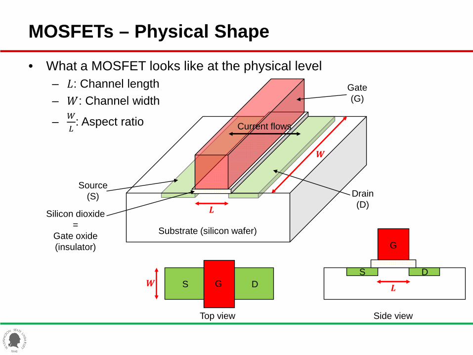
MOSFETs – Physical Shape
• What a MOSFET looks like at the physical level – 𝐿𝐿: Channel length – 𝑊𝑊: Channel width
– 𝑊𝑊𝐿𝐿
: Aspect ratio
Substrate (silicon wafer)
Drain (D)
Source (S)
Silicon dioxide =
Gate oxide (insulator)
𝑳𝑳
Gate (G)
𝑾𝑾
S D
G
𝑳𝑳 G S D 𝑾𝑾
Top view Side view
Current flows

MOSFETs – Physical Shape
• Inverter
Source: Neil H. Weste and David M. Harris, “CMOS VLSI Design: A Circuits and Systems Perspective,” 2011
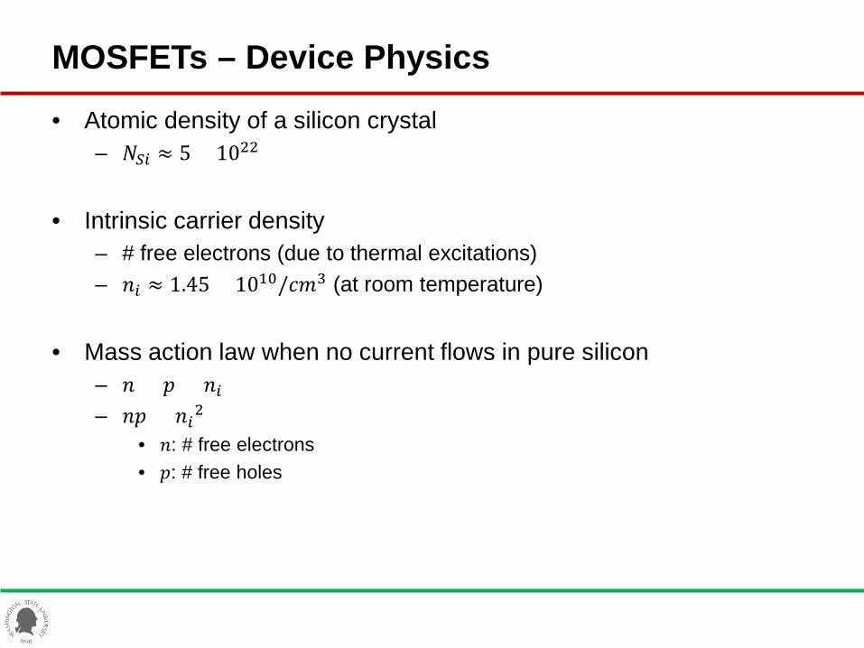
MOSFETs – Device Physics
• Atomic density of a silicon crystal – 𝑁𝑁𝑆𝑆𝑆𝑆 ≈ 5 × 10²²
• Intrinsic carrier density
– # free electrons (due to thermal excitations) – 𝑛𝑛𝑆𝑆 ≈ 1.45 × 10¹⁰/𝑐𝑐𝑚𝑚3 (at room temperature)
• Mass action law when no current flows in pure silicon
– 𝑛𝑛 = 𝑝𝑝 = 𝑛𝑛𝑆𝑆 – 𝑛𝑛𝑝𝑝 = 𝑛𝑛𝑆𝑆2
• 𝑛𝑛: # free electrons • 𝑝𝑝: # free holes

MOSFETs – Device Physics
• Doping – Add impurity atoms (dopants) to enhance # electrons or # holes. – n-type material: if more electrons are added (donors).
• 𝑁𝑁𝑑𝑑: # donors (1016~1019/𝑐𝑐𝑚𝑚3) • # free electrons (majority carriers): 𝑛𝑛𝑛𝑛 ≈ 𝑁𝑁𝑑𝑑/𝑐𝑐𝑚𝑚3
• # holes (minority carriers): 𝑝𝑝𝑛𝑛 ≈𝑛𝑛𝑖𝑖2
𝑁𝑁𝑑𝑑/𝑐𝑐𝑚𝑚3
• 𝑛𝑛𝑛𝑛 ≫ 𝑝𝑝𝑛𝑛 – p-type material: if more holes are added (acceptors).
• 𝑁𝑁𝑎𝑎: # acceptors (1014~1019/𝑐𝑐𝑚𝑚3) • # holes (majority carriers): 𝑝𝑝𝑝𝑝 ≈ 𝑁𝑁𝑎𝑎/𝑐𝑐𝑚𝑚3
• # free electrons (minority carriers): 𝑛𝑛𝑝𝑝 ≈𝑛𝑛𝑖𝑖2
𝑁𝑁𝑎𝑎/𝑐𝑐𝑚𝑚3
• 𝑝𝑝𝑝𝑝 ≫ 𝑛𝑛𝑝𝑝
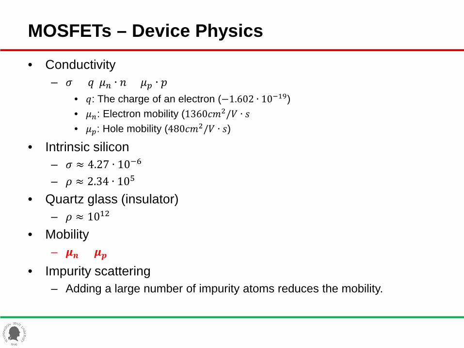
MOSFETs – Device Physics
• Conductivity – 𝜎𝜎 = 𝑞𝑞(𝜇𝜇𝑛𝑛 ∙ 𝑛𝑛 + 𝜇𝜇𝑝𝑝 ∙ 𝑝𝑝)
• 𝑞𝑞: The charge of an electron (−1.602 ∙ 10−19) • 𝜇𝜇𝑛𝑛: Electron mobility (1360𝑐𝑐𝑚𝑚2/𝑉𝑉 ∙ 𝑠𝑠) • 𝜇𝜇𝑝𝑝: Hole mobility (480𝑐𝑐𝑚𝑚2/𝑉𝑉 ∙ 𝑠𝑠)
• Intrinsic silicon – 𝜎𝜎 ≈ 4.27 ∙ 10−6 – 𝜌𝜌 ≈ 2.34 ∙ 105
• Quartz glass (insulator) – 𝜌𝜌 ≈ 1012
• Mobility – 𝝁𝝁𝒏𝒏 > 𝝁𝝁𝒑𝒑
• Impurity scattering – Adding a large number of impurity atoms reduces the mobility.

PN Junction
p
n
p
n
p
n
Forward current
𝐼𝐼 > 0
𝐼𝐼 > 0 𝐼𝐼 = 0
𝐼𝐼 = 0
Reverse blocking pn junction
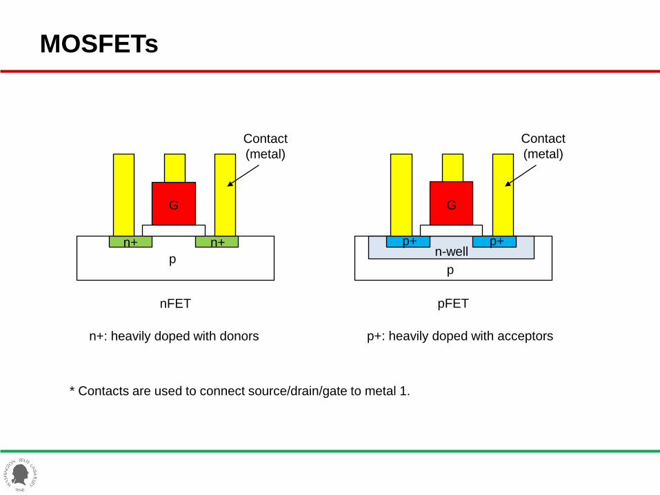
MOSFETs
n+ n+
G
nFET
n+: heavily doped with donors
p
Contact (metal)
p+ p+
G
pFET
p+: heavily doped with acceptors
p
Contact (metal)
n-well
* Contacts are used to connect source/drain/gate to metal 1.

MOSFETs – Device Physics
• 𝑡𝑡𝑜𝑜𝑜𝑜: oxide thickness – Typically a few nm
• Gate material – Polysilicon (called poly) – Metal
• Oxide capacitance (Gate(M) – Insulator(O) – Semiconductor(S)) – 𝐶𝐶𝐺𝐺 = 𝑐𝑐𝑜𝑜𝑜𝑜 ∙ 𝐴𝐴𝐺𝐺
• 𝑐𝑐𝑜𝑜𝑜𝑜 = 𝜀𝜀𝑜𝑜𝑜𝑜𝑡𝑡𝑜𝑜𝑜𝑜
: unit gate capacitance
– 𝜀𝜀𝑜𝑜𝑜𝑜 ≈ 3.9𝜀𝜀0 = 3.9 ∙ 8.854 ∙ 10−12𝐹𝐹/𝑚𝑚 • 𝐴𝐴𝐺𝐺: gate area (= 𝐿𝐿 ∙ 𝑊𝑊)
– Example • 𝑡𝑡𝑜𝑜𝑜𝑜 = 8𝑛𝑛𝑚𝑚, 𝐿𝐿 = 45𝑛𝑛𝑚𝑚,𝑊𝑊 = 70𝑛𝑛𝑚𝑚
– 𝐶𝐶𝐺𝐺 ≈ 0.013𝑓𝑓𝐹𝐹
G
𝑉𝑉𝐺𝐺
𝑡𝑡𝑜𝑜𝑜𝑜

MOSFETs – Device Physics (nFET)
• Current – Channel charge: 𝑄𝑄𝑐𝑐 = −𝐶𝐶𝐺𝐺(𝑉𝑉𝐺𝐺 − 𝑉𝑉𝑇𝑇𝑛𝑛)
• No charge forms until 𝑉𝑉𝐺𝐺 reaches 𝑉𝑉𝑇𝑇𝑛𝑛.
– Current flowing the channel: 𝐼𝐼 = |𝑄𝑄𝑐𝑐|𝜏𝜏𝑡𝑡
• 𝜏𝜏𝑡𝑡 = 𝐿𝐿𝑣𝑣: channel transit time (the average time needed for an electron to
move from S to D).
• 𝑣𝑣 = 𝜇𝜇𝑛𝑛 ∙ 𝐸𝐸 = 𝜇𝜇𝑛𝑛 ∙𝑉𝑉𝐷𝐷𝐷𝐷𝐿𝐿
– 𝑰𝑰 ≈ 𝝁𝝁𝒏𝒏 ∙ 𝒄𝒄𝒐𝒐𝒐𝒐 ∙𝑾𝑾𝑳𝑳
∙ (𝑽𝑽𝑮𝑮 − 𝑽𝑽𝑻𝑻𝒏𝒏) ∙ 𝑽𝑽𝑫𝑫𝑫𝑫
n+ n+
G
p
𝑉𝑉𝐺𝐺 = 0
n+ n+
G
p
𝑉𝑉𝐺𝐺 > 0
electrons
𝑳𝑳

MOSFETs – Device Physics (nFET)
• Current through the channel
– 𝐼𝐼 ≈ 𝜇𝜇𝑛𝑛 ∙ 𝑐𝑐𝑜𝑜𝑜𝑜 ∙𝑊𝑊𝐿𝐿
∙ 𝑉𝑉𝐺𝐺 − 𝑉𝑉𝑇𝑇𝑛𝑛 ∙ 𝑉𝑉𝐷𝐷𝑆𝑆 = 𝛽𝛽𝑛𝑛 ∙ 𝑉𝑉𝐺𝐺 − 𝑉𝑉𝑇𝑇𝑛𝑛 ∙ 𝑉𝑉𝐷𝐷𝑆𝑆
• 𝛽𝛽𝑛𝑛 = 𝜇𝜇𝑛𝑛 ∙ 𝑐𝑐𝑜𝑜𝑜𝑜 ∙𝑊𝑊𝐿𝐿
: device transconductance • 𝜇𝜇𝑛𝑛, 𝑐𝑐𝑜𝑜𝑜𝑜 ,𝑉𝑉𝑇𝑇𝑛𝑛: constants • 𝐿𝐿,𝑊𝑊: variables (designers can decide) • 𝑉𝑉𝐺𝐺 ,𝑉𝑉𝐷𝐷𝑆𝑆: variables (but either 0 or 𝑉𝑉𝐷𝐷𝐷𝐷)
• Channel resistance
– 𝑅𝑅𝑛𝑛 = 𝑉𝑉𝐷𝐷𝐷𝐷𝐼𝐼
= 1𝛽𝛽𝑛𝑛∙(𝑉𝑉𝐺𝐺−𝑉𝑉𝑇𝑇𝑛𝑛)
n+ n+
G
p
𝑉𝑉𝐺𝐺 > 𝑉𝑉𝑇𝑇𝑛𝑛
Channel resistance

MOSFETs – Device Physics (pFET)
• Current – Channel charge: 𝑄𝑄𝑐𝑐 = 𝐶𝐶𝐺𝐺(𝑉𝑉𝐺𝐺 − 𝑉𝑉𝑇𝑇𝑝𝑝 )
• No charge forms until 𝑉𝑉𝐺𝐺 reaches 𝑉𝑉𝐷𝐷𝐷𝐷 − |𝑉𝑉𝑇𝑇𝑝𝑝|.
– Current flowing the channel: 𝐼𝐼 = |𝑄𝑄𝑐𝑐|𝜏𝜏𝑡𝑡
• 𝜏𝜏𝑡𝑡 = 𝐿𝐿𝑣𝑣: channel transit time (the average time needed for an electron to
move from D to S).
• 𝑣𝑣 = 𝜇𝜇𝑝𝑝 ∙ 𝐸𝐸 = 𝜇𝜇𝑝𝑝 ∙𝑉𝑉𝐷𝐷𝐷𝐷𝐿𝐿
– 𝑰𝑰 ≈ 𝝁𝝁𝒑𝒑 ∙ 𝒄𝒄𝒐𝒐𝒐𝒐 ∙𝑾𝑾𝑳𝑳
∙ (𝑽𝑽𝑮𝑮 − 𝑽𝑽𝑻𝑻𝒑𝒑 ) ∙ 𝑽𝑽𝑫𝑫𝑫𝑫
p+ p+
G
n
𝑉𝑉𝐺𝐺 = 𝑉𝑉𝐷𝐷𝐷𝐷
p+ p+
G
n
𝑉𝑉𝐺𝐺 < 𝑉𝑉𝐷𝐷𝐷𝐷 − |𝑉𝑉𝑇𝑇𝑝𝑝|
holes
𝑳𝑳

MOSFETs – Device Physics
• Current through the channel
– 𝐼𝐼 ≈ 𝜇𝜇𝑝𝑝 ∙ 𝑐𝑐𝑜𝑜𝑜𝑜 ∙𝑊𝑊𝐿𝐿
∙ 𝑉𝑉𝐺𝐺 − 𝑉𝑉𝑇𝑇𝑝𝑝 ∙ 𝑉𝑉𝑆𝑆𝐷𝐷 = 𝛽𝛽𝑝𝑝 ∙ 𝑉𝑉𝐺𝐺 − 𝑉𝑉𝑇𝑇𝑝𝑝 ∙ 𝑉𝑉𝑆𝑆𝐷𝐷
• 𝛽𝛽𝑝𝑝 = 𝜇𝜇𝑝𝑝 ∙ 𝑐𝑐𝑜𝑜𝑜𝑜 ∙𝑊𝑊𝐿𝐿
: device transconductance
• 𝜇𝜇𝑝𝑝, 𝑐𝑐𝑜𝑜𝑜𝑜 ,𝑉𝑉𝑇𝑇𝑝𝑝: constants • 𝐿𝐿,𝑊𝑊: variables (designers can decide) • 𝑉𝑉𝐺𝐺 ,𝑉𝑉𝑆𝑆𝐷𝐷: variables (but either 0 or 𝑉𝑉𝐷𝐷𝐷𝐷)
• Channel resistance
– 𝑅𝑅𝑝𝑝 = 𝑉𝑉𝐷𝐷𝐷𝐷𝐼𝐼
= 1𝛽𝛽𝑝𝑝∙(𝑉𝑉𝐺𝐺− 𝑉𝑉𝑇𝑇𝑝𝑝 )
p+ p+
G
p
𝑉𝑉𝐺𝐺 < 𝑉𝑉𝐷𝐷𝐷𝐷 − |𝑉𝑉𝑇𝑇𝑝𝑝|
Channel resistance

MOSFETs – Device Physics
• Charging the gate requires current flows. – 𝑖𝑖 = 𝐶𝐶𝐺𝐺
𝑑𝑑𝑉𝑉𝐺𝐺𝑑𝑑𝑡𝑡
– The transistor itself has a signal delay. – If 𝐶𝐶𝐺𝐺 is large, the delay goes up.
• Energy
– 𝐸𝐸 = ∫𝑃𝑃 𝑑𝑑𝑡𝑡 = ∫ 𝑉𝑉 ∙ 𝐼𝐼 𝑑𝑑𝑡𝑡 = ∫ 𝑉𝑉 ∙ 𝐶𝐶 𝑑𝑑𝑉𝑉𝑑𝑑𝑡𝑡
𝑑𝑑𝑡𝑡 = 12𝐶𝐶𝑉𝑉2
– 𝐸𝐸 = 12𝐶𝐶𝐺𝐺𝑉𝑉𝐷𝐷𝐷𝐷2
– Driving a transistor consumes energy (power dissipation).