PHY 201 (Blum) Transistors and Logic Gates References: .
42
PHY 201 (Blum) Transistors and Logic Gates References: http://www.st-and.ac.uk/~www_pa/Scots_Guide/info/comp/active/ BiPolar/page1.html
-
Upload
roman-sarver -
Category
Documents
-
view
215 -
download
0
Transcript of PHY 201 (Blum) Transistors and Logic Gates References: .

PHY 201 (Blum)
Transistors and Logic Gates
References:http://www.st-and.ac.uk/~www_pa/Scots_Guide/info/comp/active/BiPolar/page1.html
PHY 201 (Blum)
Transistors There are various kinds of transistors:
bipolar, field-effect, etc. They differ in stability, energy usage, and so
on, but they serve a similar purpose. They are used to amplify a signal or to act
as a switch. It is as switches that they are used in computers. The change from vacuum tubes to transistors
meant dramatic differences in the physical size of computers and ultimately dramatic differences in their speed, capacity and ubiquity.

PHY 201 (Blum)
Generations
Computers are thought of as belonging to generations.
For the ENIAC and other computers of the first generation, the processor was comprised of vacuum tubes.
The processor’s individual vacuum tubes were replaced by individual transistors in the second generation of computers.
Several transistors could be placed close together on an integrated circuit (IC) or chip. In third generation computers the processor consisted of several IC’s.
PHY 201 (Blum)
Processor Microprocessor Eventually the entire processor was
placed on a single chip. When this became standard computers were said to enter the fourth generation. In this case, the processor is known as a
microprocessor. Some large machines today may have
the processor spread over more than chip. But PCs typically have a single processor.
PHY 201 (Blum)
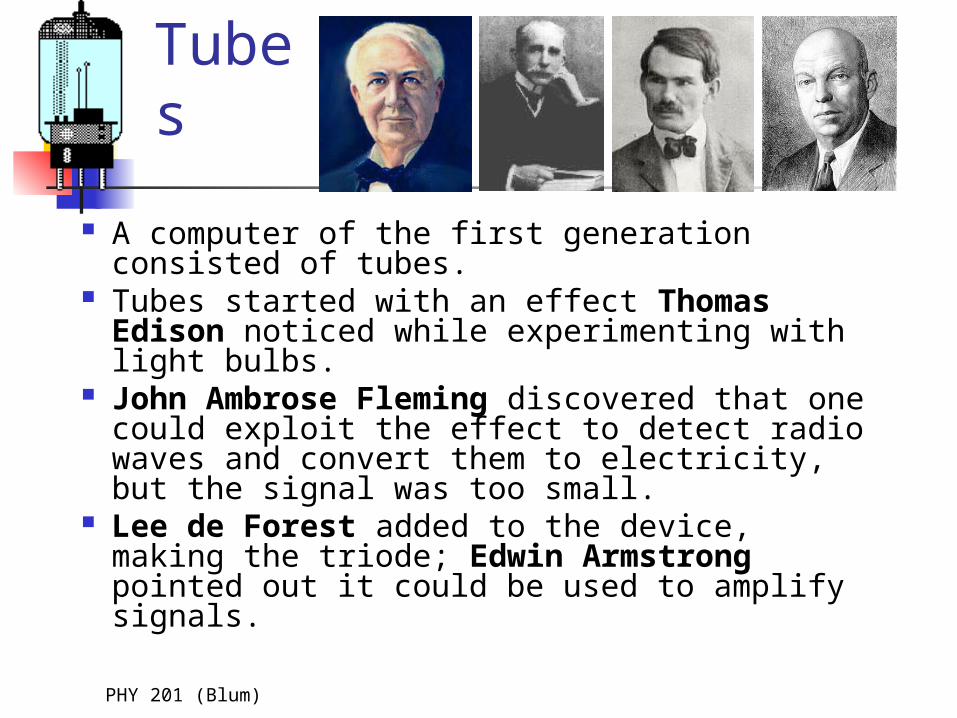
Tubes
A computer of the first generation consisted of tubes.
Tubes started with an effect Thomas Edison noticed while experimenting with light bulbs.
John Ambrose Fleming discovered that one could exploit the effect to detect radio waves and convert them to electricity, but the signal was too small.
Lee de Forest added to the device, making the triode; Edwin Armstrong pointed out it could be used to amplify signals.
PHY 201 (Blum)
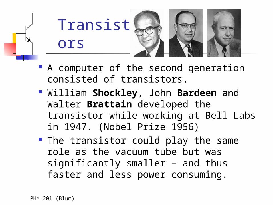
Transistors
A computer of the second generation consisted of transistors.
William Shockley, John Bardeen and Walter Brattain developed the transistor while working at Bell Labs in 1947. (Nobel Prize 1956)
The transistor could play the same role as the vacuum tube but was significantly smaller – and thus faster and less power consuming.
PHY 201 (Blum)
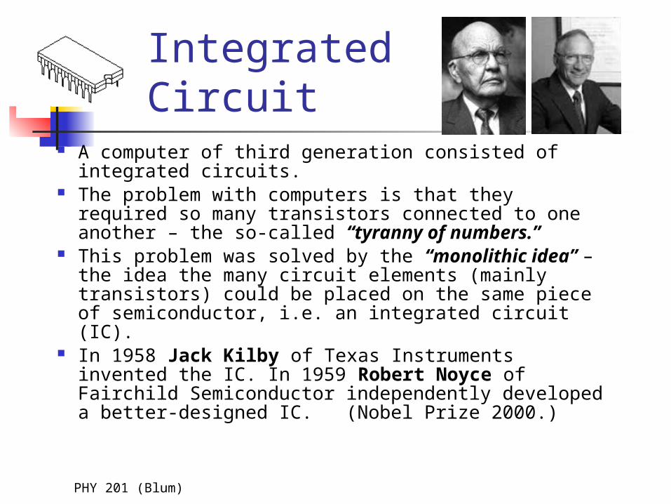
Integrated Circuit
A computer of third generation consisted of integrated circuits.
The problem with computers is that they required so many transistors connected to one another – the so-called “tyranny of numbers.”
This problem was solved by the “monolithic idea” – the idea the many circuit elements (mainly transistors) could be placed on the same piece of semiconductor, i.e. an integrated circuit (IC).
In 1958 Jack Kilby of Texas Instruments invented the IC. In 1959 Robert Noyce of Fairchild Semiconductor independently developed a better-designed IC. (Nobel Prize 2000.)
PHY 201 (Blum)
Microprocessor A computer of fourth generation has a
microprocessor. What distinguishes a microprocessor
from other integrated circuits is that a microprocessor can be programmed.
So along with the idea of the microprocessor comes the idea of the instruction set – the set of actions the programmer can have the microprocessor perform.
PHY 201 (Blum)
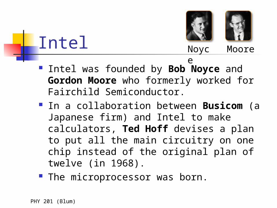
Intel Intel was founded by Bob Noyce and
Gordon Moore who formerly worked for Fairchild Semiconductor.
In a collaboration between Busicom (a Japanese firm) and Intel to make calculators, Ted Hoff devises a plan to put all the main circuitry on one chip instead of the original plan of twelve (in 1968).
The microprocessor was born.
Noyce Moore
PHY 201 (Blum)
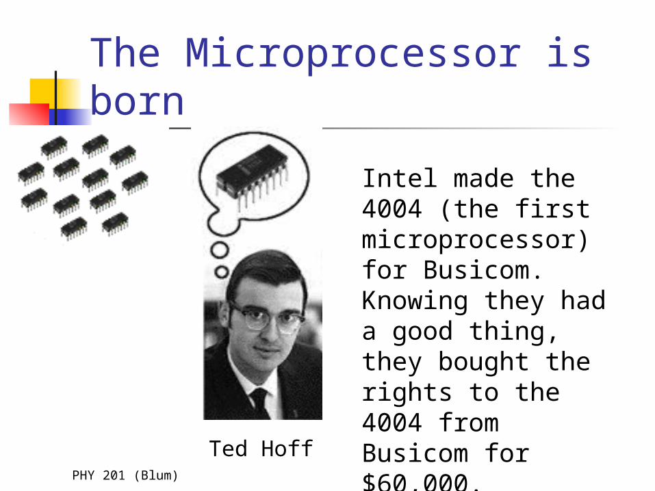
The Microprocessor is born
Intel made the 4004 (the first microprocessor) for Busicom. Knowing they had a good thing, they bought the rights to the 4004 from Busicom for $60,000.
Ted Hoff
PHY 201 (Blum)
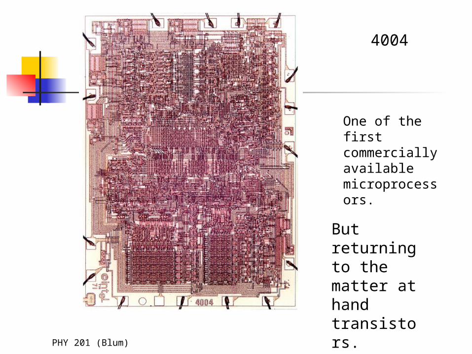
4004
One of the first commercially available microprocessors.
But returning to the matter at hand transistors.
PHY 201 (Blum)
Diode Review Recall that a pn junction — the
joining together of p-doped (“too few” electrons) and n-doped (“extra” electrons) — makes a diode.
A diode is a circuit element that allows current to flow in one direction (forward bias) but not in the other (reverse bias).

PHY 201 (Blum)
Diode Review (Cont.) Recall that a semiconductor had a full
valence band and an empty conduction band separated by a gap.
We could improve the conductivity of a semiconductor by doping it. N-doping put some electrons into the
conduction band which were free to move about.
P-doping freed up some places in the valence band – these “holes” were also free to move about.
PHY 201 (Blum)
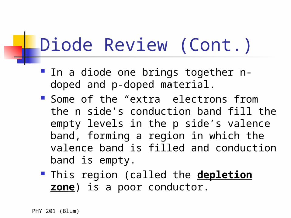
Diode Review (Cont.) In a diode one brings together n-doped
and p-doped material. Some of the “extra” electrons from the n
side’s conduction band fill the empty levels in the p side’s valence band, forming a region in which the valence band is filled and conduction band is empty.
This region (called the depletion zone) is a poor conductor.
PHY 201 (Blum)
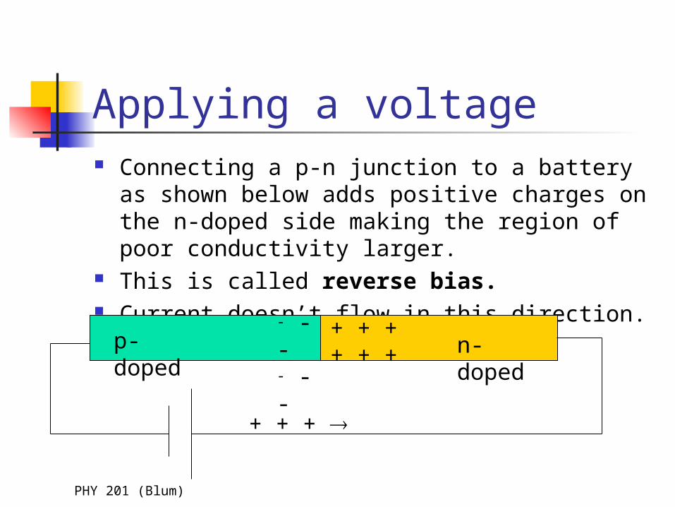
Applying a voltage Connecting a p-n junction to a battery as shown below
adds positive charges on the n-doped side making the region of poor conductivity larger.
This is called reverse bias. Current doesn’t flow in this direction.
p-doped - - -- - -
+ + + + + + n-doped
+ + +
PHY 201 (Blum)
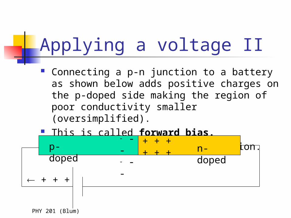
Applying a voltage II Connecting a p-n junction to a battery as shown below
adds positive charges on the p-doped side making the region of poor conductivity smaller (oversimplified).
This is called forward bias. Current does flow in this direction.
p-doped - - -- - -
+ + + + + + n-doped
+ + +
PHY 201 (Blum)
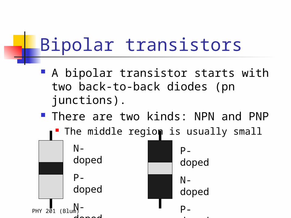
Bipolar transistors A bipolar transistor starts with two back-
to-back diodes (pn junctions). There are two kinds: NPN and PNP
The middle region is usually small
N-doped
P-doped
N-doped
P-doped
N-doped
P-doped
PHY 201 (Blum)
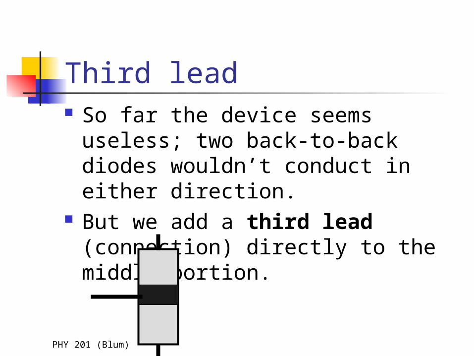
Third lead So far the device seems useless;
two back-to-back diodes wouldn’t conduct in either direction.
But we add a third lead (connection) directly to the middle portion.
PHY 201 (Blum)
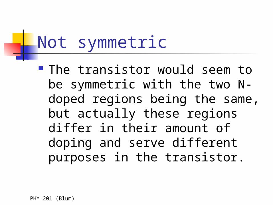
Not symmetric The transistor would seem to be
symmetric with the two N-doped regions being the same, but actually these regions differ in their amount of doping and serve different purposes in the transistor.
PHY 201 (Blum)
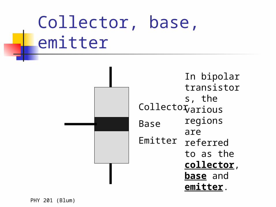
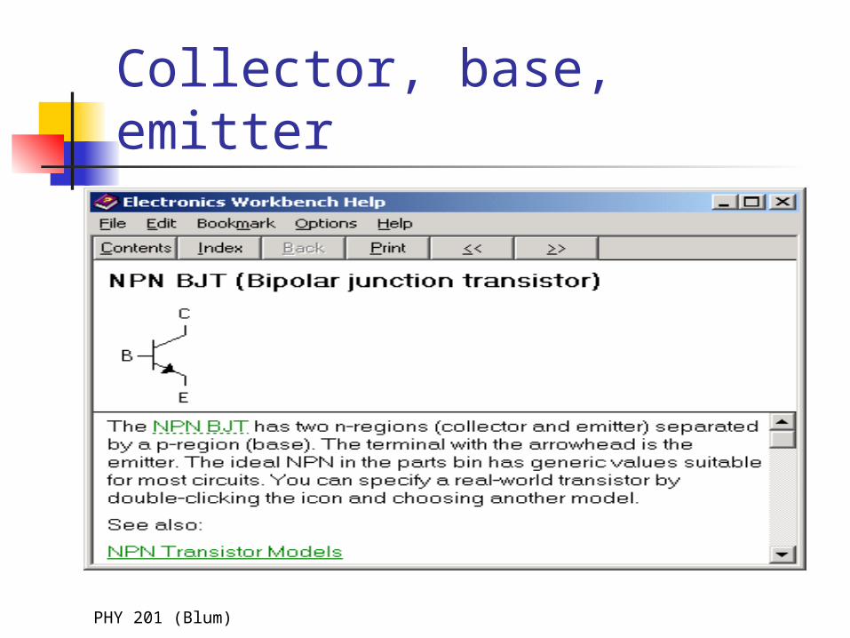
Collector, base, emitter
Collector
Base
Emitter
In bipolar transistors, the various regions are referred to as the collector, base and emitter.
PHY 201 (Blum)
Collector, base, emitter
PHY 201 (Blum)
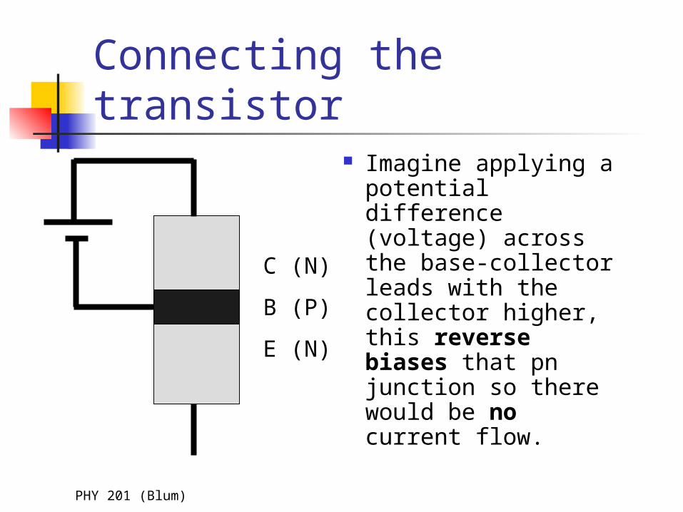
Connecting the transistor Imagine applying a
potential difference (voltage) across the base-collector leads with the collector higher, this reverse biases that pn junction so there would be no current flow.
C (N)
B (P)
E (N)
PHY 201 (Blum)
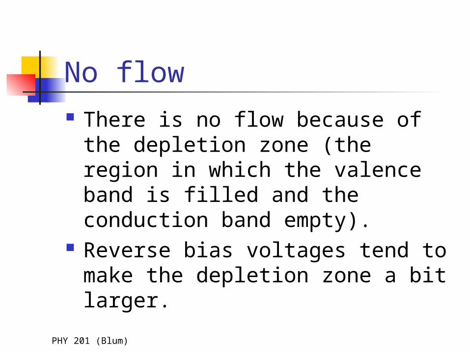
No flow There is no flow because of the
depletion zone (the region in which the valence band is filled and the conduction band empty).
Reverse bias voltages tend to make the depletion zone a bit larger.
PHY 201 (Blum)
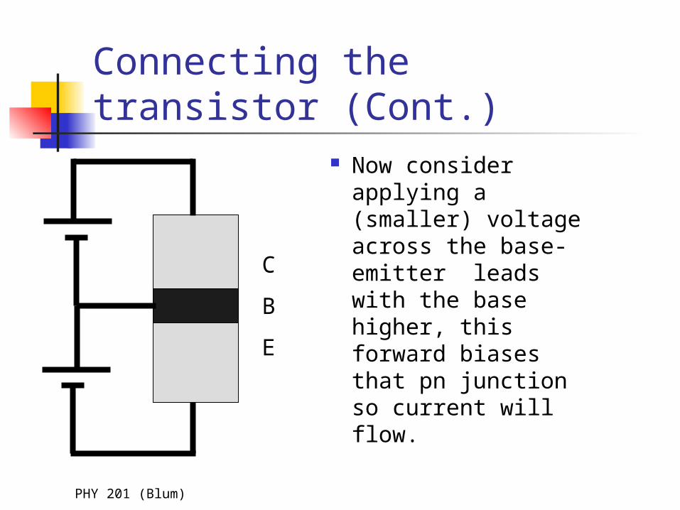
Connecting the transistor (Cont.)
Now consider applying a (smaller) voltage across the base-emitter leads with the base higher, this forward biases that pn junction so current will flow.
C
B
E
PHY 201 (Blum)
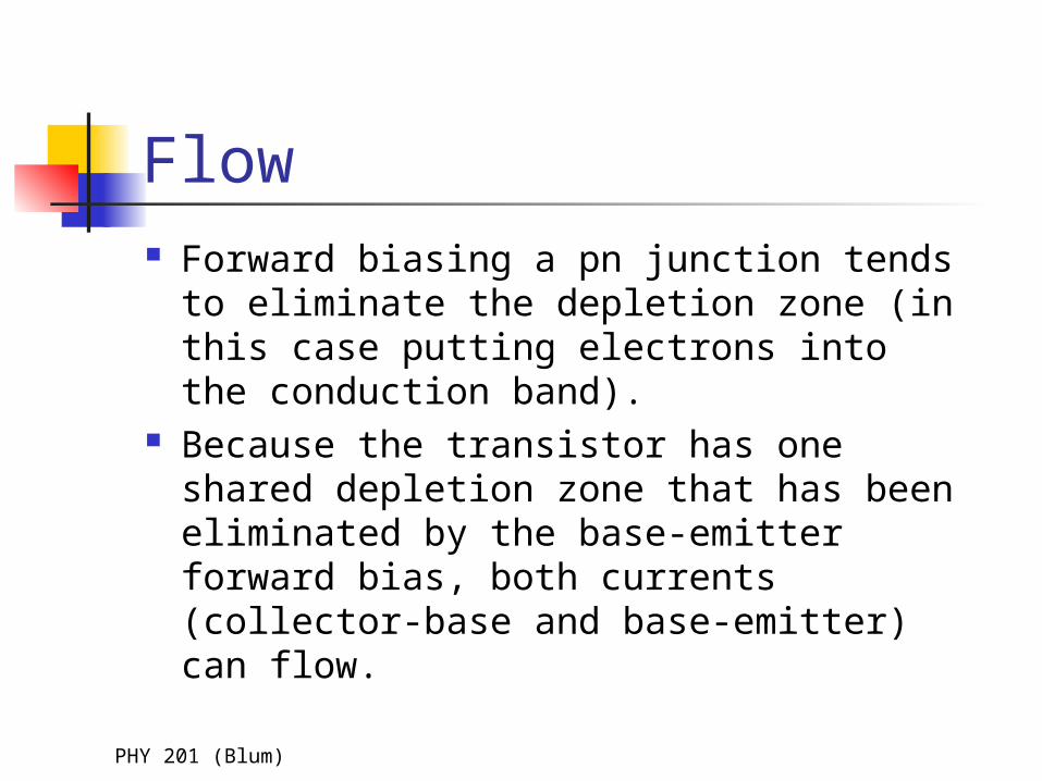
Flow Forward biasing a pn junction tends to
eliminate the depletion zone (in this case putting electrons into the conduction band).
Because the transistor has one shared depletion zone that has been eliminated by the base-emitter forward bias, both currents (collector-base and base-emitter) can flow.
PHY 201 (Blum)
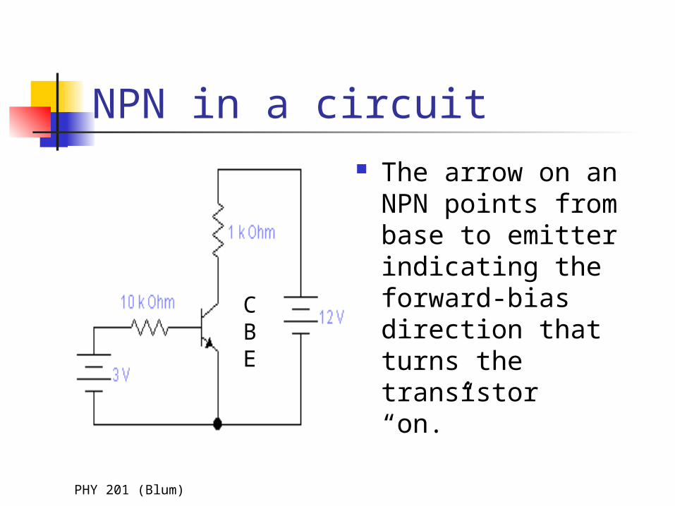
NPN in a circuit The arrow on an
NPN points from base to emitter indicating the forward-bias direction that turns the transistor “on.”
CBE
PHY 201 (Blum)
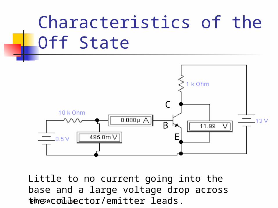
Characteristics of the Off State
B
C
E
Little to no current going into the base and a large voltage drop across the collector/emitter leads.
PHY 201 (Blum)
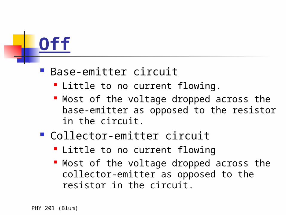
Off Base-emitter circuit
Little to no current flowing. Most of the voltage dropped across the
base-emitter as opposed to the resistor in the circuit.
Collector-emitter circuit Little to no current flowing Most of the voltage dropped across the
collector-emitter as opposed to the resistor in the circuit.
PHY 201 (Blum)
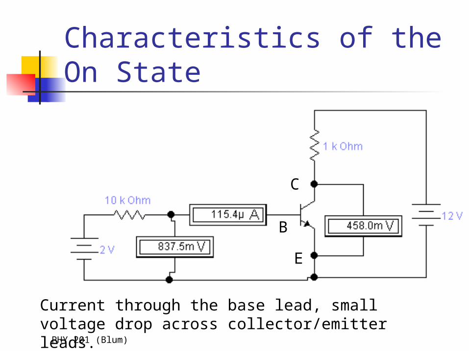
Characteristics of the On State
C
B
E
Current through the base lead, small voltage drop across collector/emitter leads.
PHY 201 (Blum)
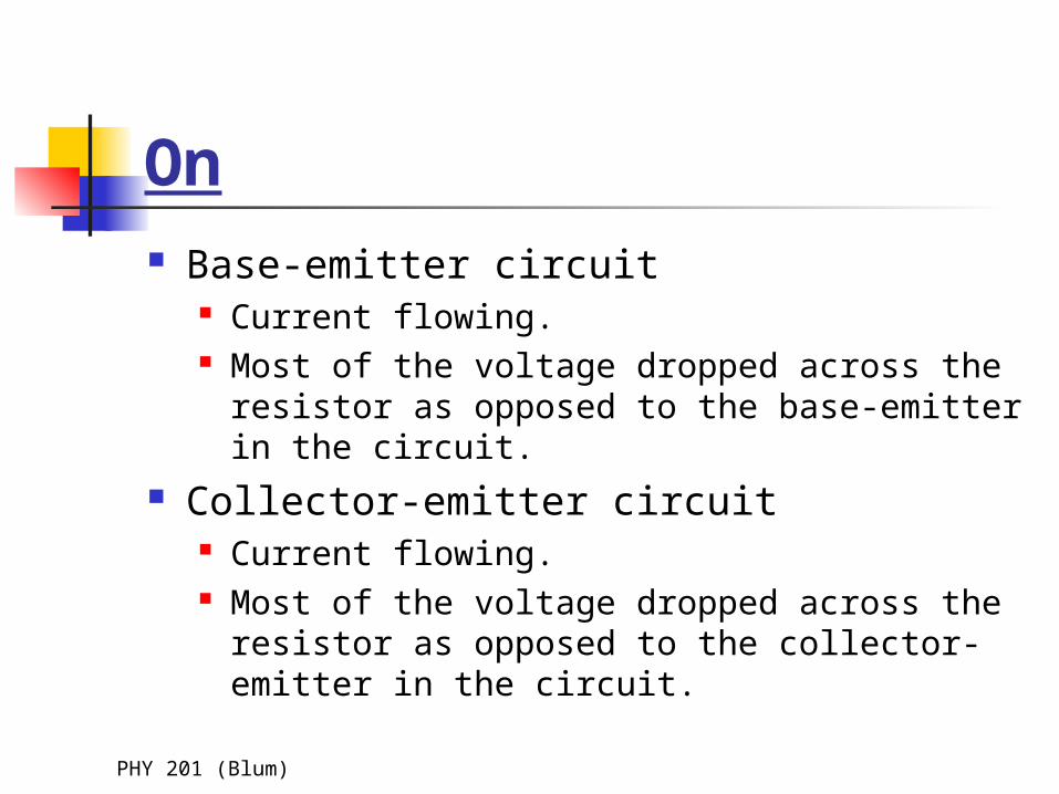
On Base-emitter circuit
Current flowing. Most of the voltage dropped across the
resistor as opposed to the base-emitter in the circuit.
Collector-emitter circuit Current flowing. Most of the voltage dropped across the
resistor as opposed to the collector-emitter in the circuit.
PHY 201 (Blum)
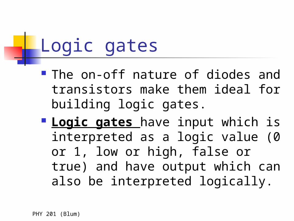
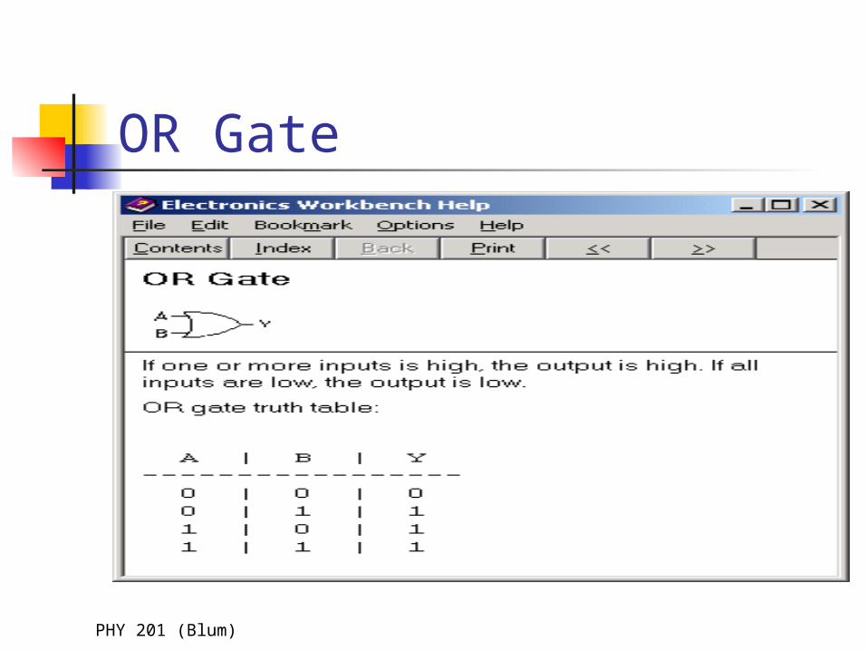
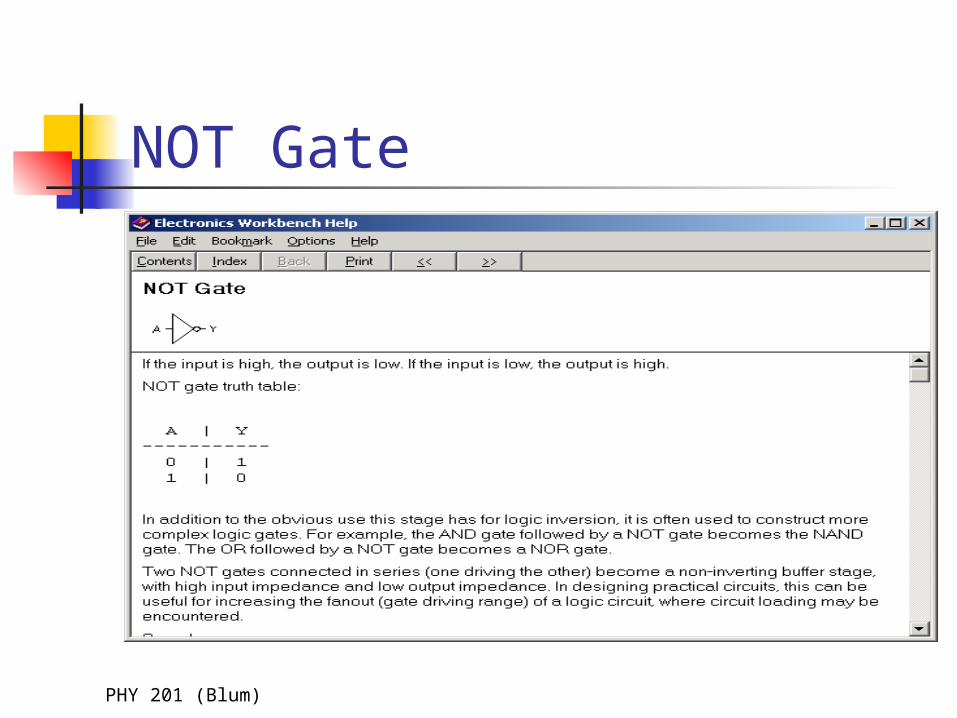
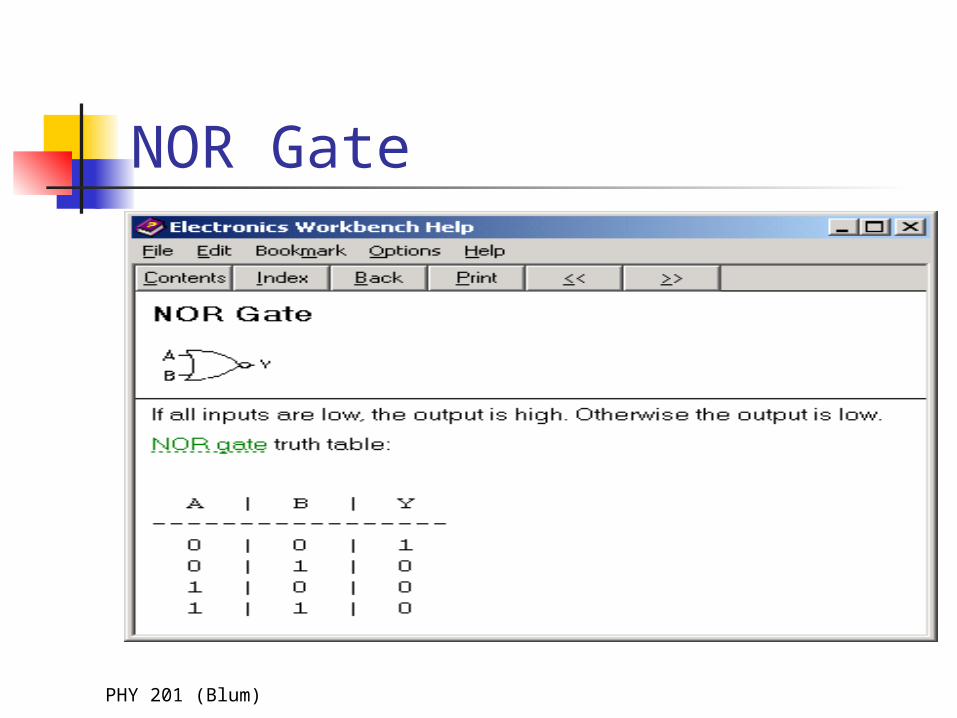
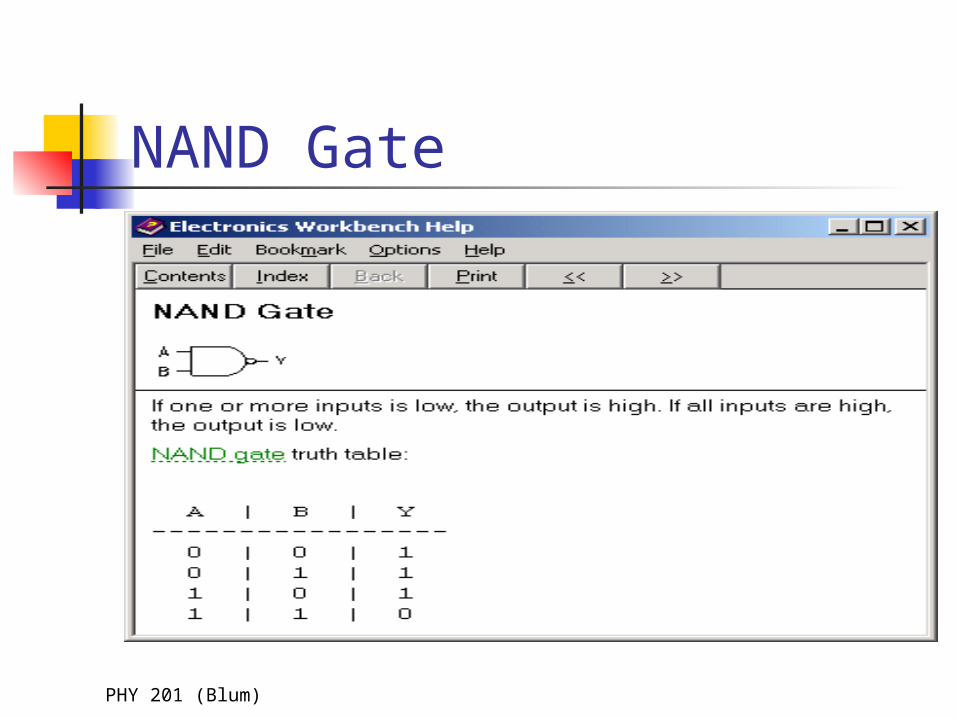
Logic gates The on-off nature of diodes and
transistors make them ideal for building logic gates.
Logic gates have input which is interpreted as a logic value (0 or 1, low or high, false or true) and have output which can also be interpreted logically.
PHY 201 (Blum)
Logic gates
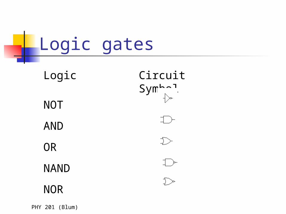
Logic Circuit Symbol
NOT
AND
OR
NAND
NOR
PHY 201 (Blum)
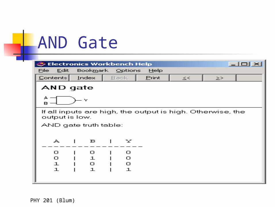
AND Gate
PHY 201 (Blum)
OR Gate
PHY 201 (Blum)
NOT Gate
PHY 201 (Blum)
NOR Gate
PHY 201 (Blum)
NAND Gate
PHY 201 (Blum)
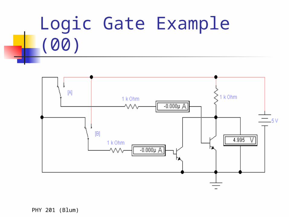
Logic Gate Example (00)

PHY 201 (Blum)
Logic Gate Example (01)
PHY 201 (Blum)
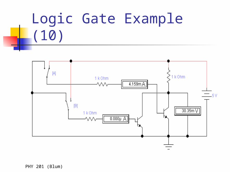
Logic Gate Example (10)

PHY 201 (Blum)
Logic Gate Example (11)

PHY 201 (Blum)
NOR
A B Out
0 0 1
0 1 0
1 0 0
1 1 0