
Photovoltaics and Energy management Photovoltaics & Energy Management 3 The Photovoltaics and Energy...
16
PHOTOVOLTAICS & ENERGY MANAGEMENT @ WWW.CSEM.CH PV-ENERGY@CSEM.CH
Transcript of Photovoltaics and Energy management Photovoltaics & Energy Management 3 The Photovoltaics and Energy...
2
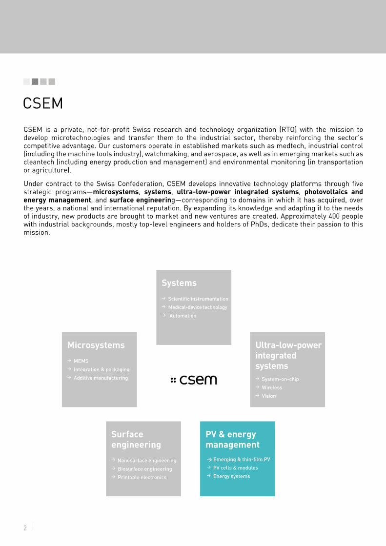
CSEM is a private, not-for-profit Swiss research and technology organization (RTO) with the mission to develop microtechnologies and transfer them to the industrial sector, thereby reinforcing the sector’s competitive advantage. Our customers operate in established markets such as medtech, industrial control (including the machine tools industry), watchmaking, and aerospace, as well as in emerging markets such as cleantech (including energy production and management) and environmental monitoring (in transportation or agriculture).
Under contract to the Swiss Confederation, CSEM develops innovative technology platforms through five strategic programs—microsystems, systems, ultra-low-power integrated systems, photovoltaics and energy management, and surface engineering—corresponding to domains in which it has acquired, over the years, a national and international reputation. By expanding its knowledge and adapting it to the needs of industry, new products are brought to market and new ventures are created. Approximately 400 people with industrial backgrounds, mostly top-level engineers and holders of PhDs, dedicate their passion to this mission.
Systems> Scientific instrumentation> Medical-device technology> Automation
Surface engineering> Nanosurface engineering> Biosurface engineering> Printable electronics
Microsystems> MEMS > Integration & packaging> Additive manufacturing
Ultra-low-power integrated systems> System-on-chip > Wireless> Vision
CSEM
PV & energy management> Emerging & thin-film PV > PV cells & modules> Energy systems
Photovoltaics & Energy Management 3
The Photovoltaics and Energy Management (PV&E) program is an industry-driven, application-oriented program within CSEM with the aim of fostering innovation and accelerating the pace of technology transfer in the fields of photovoltaics and energy storage and systems, as well as in new market segments such as energy scavenging and the Internet of Things.
We develop innovative process technologies, device concepts, and new high-tech solutions to better serve the Swiss and global renewable energy industry. More generally, the PV&E program targets the following objectives:
− To provide cutting-edge innovation in the field of photovoltaic devices, realizing the best devices with a high potential for industrialization, from advanced crystalline silicon to multi-junction solar cells.
− To design and develop highly reliable modules, for the power market, for the transportation sector, or with the highest potential for adoption by the public in the built environment.
− To support the development of next-generation equipment and metrology systems, all along the value chain of photovoltaics, creating a sustainable cleantech value for existing and future CSEM customers.
− To provide new solutions for specialized devices, coatings, or materials with higher added value, and for PV components with enhanced functionalities.
− To bring solutions to the energy/electricity management field, as we transition toward a society essentially powered by renewables, in which energy efficiency and management will be realized through intelligent hardware and algorithms.
To meet these challenging objectives and to support the transition to an energy system in which solar will play an essential role, CSEM and its PV&E team collaborate closely with the Swiss Federal Institute of Technology EPFL and its photovoltaics and thin electronics laboratory PV-Lab, with Swiss universities and universities of applied sciences (SUPSI and BHF), as well as with international organizations or agencies.
Photovoltaics & Energy Management
Emerging & thin-film PV
Energy systems
PV cells & modules
Infrastructure
4
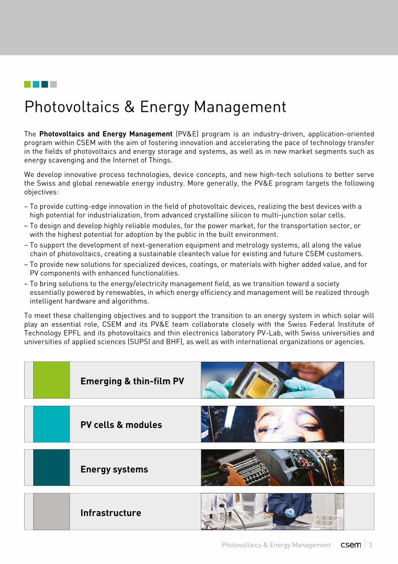
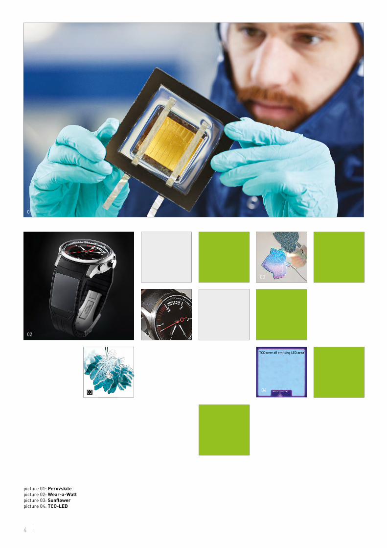
picture 01: Perovskitepicture 02: Wear-a-Wattpicture 03: Sunflowerpicture 04: TCO-LED
01
02 02
03 04
03
Photovoltaics & Energy Management 5
EMERGING & THIN-FILM PV
In this activity, CSEM provides industry with a high level of expertise regarding customized PV cells for product integration. It also makes available its know-how in coatings for optoelectronics applications for the solution of diverse industrial challenges. The synergetic team applies laser patterning, thin-film deposition, printing methods, and device technology to design and produce cells that meet the most challenging demands, thanks to top-level facilities and latest-generation equipment.
At the same time CSEM prepares the future of PV, with new materials and cell architectures from the forefront of academic research. In this aspect of its activity, CSEM explores more efficient and cheaper solar cells in collaboration with world-leading institutes and universities.
These two parts of the activity tackle challenges in the following fields.
Customized PV
− Series production of customized solar cells − Development of flexible solar cells (based on OPV and thin-film silicon technologies).
− Integration of PV cells into final products (thin-film, III—V, crystalline silicon, OPV).
− Development of complete energy harvesting systems.
− Benchmarking of cell technologies for various applications.
Thin-film coatings and patterning
− State-of-the art transparent conductive coatings and electrodes for smart sensing and detectors.
− Light management, and microstructured substrates, films, and foils.
− Materials and processes for opto-electronics (LED, OLED, TFT, sensors, smart windows, and PV).
− Multifunctional coatings and layers for decorative, lubricating, and/or electronics applications.
Emerging PV
− Development of advanced cell concepts and PV materials with printable PV.
− High-efficiency perovskite solar cells, IR transparent perovskites, and multi-junction cells.
Our applications have been demonstrated in the field of energy harvesting, for different products ranging from watches to smart farming. The activity is complemented by a network of CSEM professionals who combine our energy-harvesting solutions with ultra-low-power designs to make the Internet of Things and wearables fully autonomous. In CSEM, our customers find a one-stop-shop for their most demanding projects, and a reliable partner who can help them turn their ideas into successful products.
6
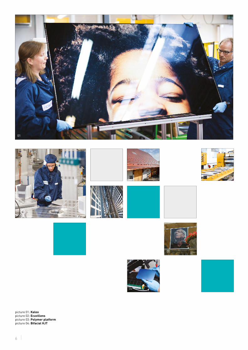
picture 01: Kaleopicture 02: Ecuvillenspicture 03: Polymer platformpicture 04: Bifacial HJT
01
04
02 03
01
Photovoltaics & Energy Management 7
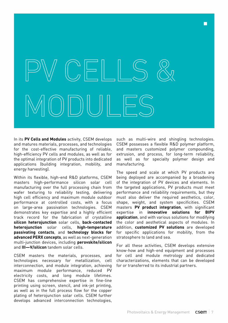
PV CELLS & MODULES
In its PV Cells and Modules activity, CSEM develops and matures materials, processes, and technologies for the cost-effective manufacturing of reliable, high-efficiency PV cells and modules, as well as for the optimal integration of PV products into dedicated applications (building integration, mobility, and energy harvesting).
Within its flexible, high-end R&D platforms, CSEM masters high-performance silicon solar cell manufacturing over the full processing chain from wafer texturing to reliability testing, delivering high cell efficiency and maximum module outdoor performance at controlled costs, with a focus on large-area passivation technologies. CSEM demonstrates key expertise and a highly efficient track record for the fabrication of crystalline silicon heterojunction solar cells, back-contacted heterojunction solar cells, high-temperature passivating contacts, and technology blocks for advanced PERX concepts, as well as next-generation multi-junction devices, including perovskite/silicon and III—V/silicon tandem solar cells.
CSEM masters the materials, processes, and technologies necessary for metallization, cell interconnection, and module integration, achieving maximum module performance, reduced PV electricity costs, and long module lifetimes. CSEM has comprehensive expertise in fine-line printing using screen, stencil, and ink-jet printing, as well as in the full process flow for the copper plating of heterojunction solar cells. CSEM further develops advanced interconnection technologies,
such as multi-wire and shingling technologies. CSEM possesses a flexible R&D polymer platform, and masters customized polymer compounding, extrusion, and process, for long-term reliability, as well as for specialty polymer design and manufacturing.
The speed and scale at which PV products are being deployed are accompanied by a broadening of the integration of PV devices and elements. In the targeted applications, PV products must meet performance and reliability requirements, but they must also deliver the required aesthetics, color, shape, weight, and system specificities. CSEM masters PV product integration, with significant expertise in innovative solutions for BIPV application, and with various solutions for modifying the color and aesthetical aspects of modules. In addition, customized PV solutions are developed for specific applications for mobility, from the stratosphere to land and sea.
For all these activities, CSEM develops extensive know-how and high-end equipment and processes for cell and module metrology and dedicated characterizations, elements that can be developed for or transferred to its industrial partners.
8
picture 01: Prosumerlabpicture 02: Hyperbatpicture 03: ESReCpicture 04: Sabina
02
03
04
04
01
Photovoltaics & Energy Management 9
ENERGY SYSTEMS
Within its Energy Systems activity, CSEM develops solutions to build and manage an efficient, sustainable-energy world based on distributed, renewable power generation. A multidisciplinary team brings together the skills to engineer this new world: power engineering, power electronics, signal processing, machine learning, optimization and control, and systems engineering.
We provide services and technologies in three main areas.
Digitalization: We apply artificial intelligence techniques to generate value from energy data. This includes forecasting energy production and consumption on multiple time scales, and tracking individual appliances from aggregate power measurements.
Decentralized control: We develop multi-level control from the device level to grid-interactive functions. Our solutions increase local consumption of renewable energy, system flexibility, and power quality. We focus on single- or multi-vector microgrids operating at scales ranging from single buildings to cities. With our thermal-control technologies, the energy consumption of existing buildings can be reduced while maintaining or improving user comfort.
Electricity storage in supercapacitors and batteries: We develop characterization methods and dynamic models to predict the performance of storage devices in complex operating conditions. With these models, we can also optimize the design and control of storage systems.
Applications of CSEM technologies have already been demonstrated on inverters, in direct current (DC) microgrids, and in energy management systems for residential and commercial buildings. We work with component vendors, system integrators, and utilities to turn these technologies into successful products.
10
picture 01: OCTOPUS IIpicture 02: Flashingpicture 03: Electro-platingpicture 04: Metallization picture 05: Sputtering/etchingpicture 06: PECVD
03
02
05
04
01
06
Photovoltaics & Energy Management 11
INFRA-STRUCTURE
Our R&D infrastructure covers the entire PV value chain from materials processing to power conversion. Most of the equipment is close to industrial grade yet highly versatile, which facilitates technology transfer and small series production. Our fabrication facilities are complemented by state-of-the-art characterization laboratories for materials, PV devices, and batteries, and by specialist software tools.
650 m2 cleanroom facilities for delivering state-of-the-art solutions and devices
− Wet-chemical processing for surface texturing and cleaning (mono- and multi-).
− Vacuum and non-vacuum thin-film coating deposition equipment and etching tools.
− High-temperature oven and furnace (diffusion, oxidation, hydrogenation, LPCVD…).
− Material and solar cell characterization for clearly determining the structure and properties of PV materials, devices, and systems.
− Laser processing units, and various foil-based and wafer-based microstructuration and fabrication units.
600 m2 technology lab for module fabrication, and measurement and test facilities
− PV module lamination and polymer extrusion. − Metallization and interconnection. − Module characterization and reliability testing including climatic chambers.
− Speciality products (ultra-lightweight modules and colored modules).
Shared infrastructure for battery characterization (BFH–CSEM Energy Storage Research Center)
− 40-channel battery cell tester. − 12-channel battery module tester. − Climatic chambers and refrigerated containers. − Electrochemical impedance spectroscopy.
Prototyping and testing platforms for power conversion and control
− Eight 5 kW PV system emulators and three 600 W PV module emulators.
− A 30 kVA grid emulator. − Rapid prototyping platform for power converters (inverters, battery chargers, power optimizers, etc.).
− DIgSILENT PowerFactory software package for the modelling of power grids.
In addition to its dedicated infrastructure, the PV&E program benefits from CSEM’s general microfabrication facilities (500 m2, class 100) and advanced analysis facilities (TEM, SEM, XRD, SPM…). It can also access advanced characterization tools and facilities on the Microcity site, managed by the EPFL PV-Lab, including 700 m2 of clean rooms and technology laboratories.
12
Records & recognition
A realistic approach to wearables
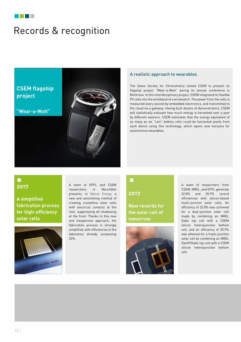
The Swiss Society for Chronometry invited CSEM to present its flagship project “Wear-a-Watt” during its annual conference in Montreux. In this interdisciplinary project, CSEM integrated its flexible PV cells into the wristband of a wristwatch. The power from the cells is measured every second by embedded electronics, and transmitted to the cloud via a gateway. Having built dozens of demonstrators, CSEM will statistically evaluate how much energy is harvested over a year by different wearers. CSEM estimates that the energy equivalent of as many as six “coin” battery cells could be harvested yearly from each device using this technology, which opens new horizons for autonomous wearables.
A team of EPFL and CSEM researchers in Neuchâtel presents, in Nature Energy, a new and astonishing method of creating crystalline solar cells with electrical contacts at the rear, suppressing all shadowing at the front. Thanks to this new and inexpensive approach, the fabrication process is strongly simplified, with efficiencies in the laboratory already surpassing 23%.
A team of researchers from CSEM, NREL, and EPFL generate 32.8% and 35.9% record efficiencies with silicon-based multi-junction solar cells. An efficiency of 32.8% was achieved for a dual-junction solar cell made by combining an NREL GaAs top cell with a CSEM silicon heterojunction bottom cell, and an efficiency of 35.9% was attained for a triple-junction solar cell by combining an NREL GaInP/GaAs top cell with a CSEM silicon heterojunction bottom cell.
2017
A simplified fabrication process for high-efficiency solar cells
2017
New records for the solar cell of tomorrow
CSEM flagship project
“Wear-a-Watt”
Photovoltaics & Energy Management 13
Integrating photovoltaic solar panels into historic, protected sites has often been a problem without a real solution. However, an important milestone has been reached in the village of Ecuvillens, located in the Swiss canton of Fribourg, where terra-cotta-red solar panels have been installed on the roof of a farmhouse, in collaboration with partners Issol and Solstis.
CSEM continues to demonstrate its commitment to turning “lab-buzzing” perovskite technology into the next probable industrial source of low-cost, high-efficiency PV devices. In 2017, CSEM demonstrated over 16% perovskite mini-module efficiency and realized—together with its academic partner, the EPFL PV-Lab—several high-efficiency perovskite/silicon devices.
The CSEM photovoltaic facade winner of the “Beauty of Solar Power Europe” photo competition 2016. At the 100 GW Celebration in Brussels (Belgium), Meyer Burger received the Solar Visualised in Europe Award for the CSEM solar facade, which includes bi-facial, high-efficiency heterojunction solar cells and invisible multi-wire connections.
The first Ex Eaquo Prize of the Umweltpreis 2016 was awarded to CSEM. Our revolutionary technology enables us to achieve what was supposed to be impossible—white and colored solar panels with no visible cells or connections. The specialty white filter, commercialized by the company Solaxess, can be applied on top of an existing module or integrated into a new module during assembly, on flat or curved surfaces.
2017
Photovoltaic solar panels were installed at protected sites
2017
Silicon–perovskite tandem cells: the next industrial solution?
2016
Swiss Environmental Prize
2016
Solar Visualised in Europe Award
14
Project descriptions
Perovskite Encapsulated perovskite single junction mini-module. Page 4
Wear-a-Watt Thin-film silicon solar cells integrated into watch dials and wristbands—from a concept to a fully functional “Wear-a-Watt”demonstrator.
Page 4
Sunflower Printed PV module with nine serially connected organic PV cell segments. Page 4
TCO-LED Blue LED using a TCO as a current-spreading layer. Page 4
Kaleo When art meet technology: any color and any design is now possible. Page 6
Ecuvillens First example of a terra-cotta colored roof based on c-Si technology. The farmhouse, in Ecuvillens, is situated in a protected historical zone.
Page 6
Polymer platform
R&D polymer platform—customized polymer compounding, extrusion, and process, for long-term reliability, as well as for specialty polymer design and manufacturing.
Page 6
Bifacial HJT High-efficiency bifacial silicon heterojunction solar cell. Page 6
Prosumerlab Prototyping platform for building energy management systems. Page 8
Hyperbat Development of a hybrid electricity storage system based on supercapacitors and batteries. Page 8
ESReC Test benches for the characterization of battery cells under charge and discharge cycles. Page 8
Sabina Calculating PV hosting capacity with CSEM’s plugin for DIgSILENT PowerFactory. Page 8
Photovoltaics & Energy Management 15
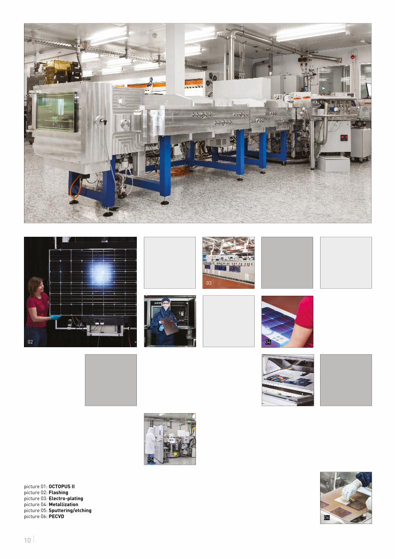
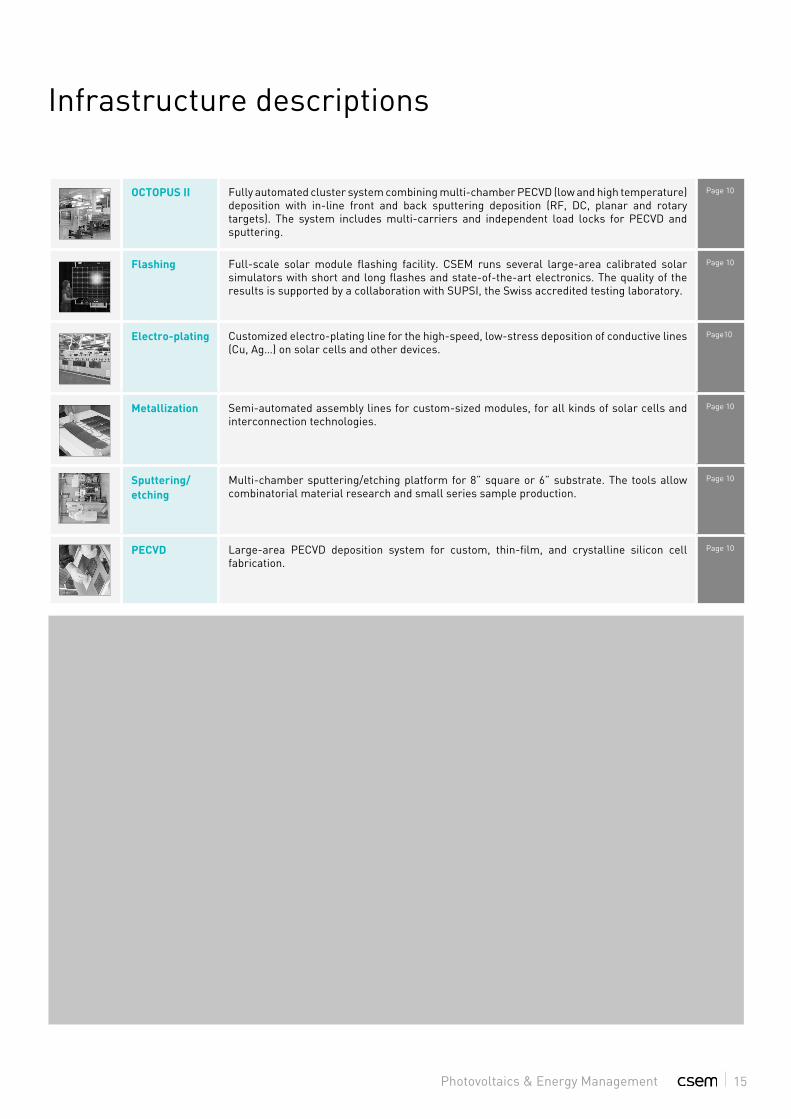
OCTOPUS II Fully automated cluster system combining multi-chamber PECVD (low and high temperature) deposition with in-line front and back sputtering deposition (RF, DC, planar and rotary targets). The system includes multi-carriers and independent load locks for PECVD and sputtering.
Page 10
Flashing Full-scale solar module flashing facility. CSEM runs several large-area calibrated solar simulators with short and long flashes and state-of-the-art electronics. The quality of the results is supported by a collaboration with SUPSI, the Swiss accredited testing laboratory.
Page 10
Electro-plating Customized electro-plating line for the high-speed, low-stress deposition of conductive lines (Cu, Ag…) on solar cells and other devices.
Page10
Metallization Semi-automated assembly lines for custom-sized modules, for all kinds of solar cells and interconnection technologies.
Page 10
Sputtering/ etching
Multi-chamber sputtering/etching platform for 8” square or 6” substrate. The tools allow combinatorial material research and small series sample production.
Page 10
PECVD Large-area PECVD deposition system for custom, thin-film, and crystalline silicon cell fabrication.
Page 10
Infrastructure descriptions