Photothermal CVD of Carbon Thin Films using CH2I2 as the Precursor
7
Photothermal CVD of Carbon Thin Films using CH 2 I 2 as the Precursor** By Abdul Rashid, LarsLandstro¨m, * Mikael Ottosson, and Klaus Piglmayer Thin carbon films are deposited via CVD from the precursor methylene iodide (CH 2 I 2 ) using two different activation sources; a broadband IR lamp and a thermal plate. Large differences in deposition rates are observed when comparing the two sources of activation. The characteristics of the deposition kinetics of the highly sensitive system are also investigated by employing a split, symmetric reactor, and by using a qualitative model. Raman spectroscopy (RS) is used for microstructural characterization of the films. The lamp technique allows a simple and low-cost experimental setup, for deposition of disordered carbon thin films at relatively low temperatures and high rates. Keywords: Carbon, Methylene iodide, IR lamp, Raman spectroscopy 1. Introduction Carbon materials are suitable for a wide range of applications and they also enable low cost and flexible components for integration within complex systems, such as electronic and photonic devices, to be developed. Intense research is ongoing in developing patterning techniques, e.g., for magnetic discs, [1–3] environmental sensors, [4] solar cells, [5] hip joints, [6] semiconductors, [7] and plastics, [8–10] and in creating new device structures and configurations for X-ray optics, [11] electrochemical detectors, [12] and clinical bioelectric measurements. [13] Opportunities can also be found in combinations of hard and soft materials, and layered structures, to combine various materials proper- ties. [14,15] Currently, carbon nanomaterials show a very high potential with respect to applications, for instance, in nanoelectronics and field emission display technology. [16–18] The intensive research in the field of carbon materials shows the need for further developments to meet the demands of future technologies. Here, some of the important features to approach are; decrease in processing temperatures, further miniaturization, modification of materials, increased flexibility, and cost effectiveness. As presently employed standard precursors usually require high apparent activation energies (i.e., high temperatures for thermal processes), and the techniques employed are often cost and/or effort intensive, and limited in versatility. We take use of the easily handled and dissociated methylene iodide (CH 2 I 2 ) in combination with various activation sources (for example, a broadband IR lamp) resulting in low costs, high versatility, and flexibility, allowing further tuning of processing parameters. Recently, deposition of thin carbon films by IR lamp- induced dissociation of CH 2 I 2 under reduced pressures was investigated. [19,20] In these preliminary reports, the large increase in deposition rate compared to standard cold-wall CVD methods (reactors of completely different geometry were used) was observed and attributed to an additional influence of photolysis effects. This idea was supported by the successful high-rate deposition experiments performed by purely photolytic dissociation of the precursor employing various UV laser systems. [21–25] At present, the methylene iodide system was investigated in further detail to try to reveal the peculiarities of the sensitive deposition processes. To allow for better control and direct comparison between lamp-induced photophysical (photon-irradiated substrate surface) and photothermal (non-irradiated surface) processes, an integrated system was used. Furthermore, standard thermal CVD processing (induced by a thermal plate) was also directly compared to lamp-activated deposition in a single cold-wall reactor. The microstructure of the thin carbon films was characterized by means of RS, and the density and hydrogen content of the deposits were estimated by X-ray reflection (XRR) and nuclear reaction analysis (NRA) measurements, respectively. DOI: 10.1002/cvde.200806666 Full Paper [*] Dr. L. Landstro ¨ m, Dr. M. Ottosson The A ˚ ngstro ¨ m Laboratory, Department of Materials Chemistry Uppsala University Box 538, SE-751 21 Uppsala (Sweden) E-mail: [email protected] Dr. L. Landstro ¨ m, Dr. A. Rashid, Dr. K. Piglmayer Institut fu ¨ r Angewandte Physik, Johannes-Kepler-Universita ¨t Linz A-4040, Linz (Austria) Dr. A. Rashid Department of Physics COMSATS Institute of Information Technology Defence Road, Off Raiwind Road Lahore (Pakistan) [**] We thank Prof. D. Ba ¨uerle for valuable discussions. One of us (L. L.) would like to thank the ‘‘Knut and Alice Wallenberg Foundation’’ for financial support. Chem. Vap. Deposition 2008, 14, 279–285 ß 2008 WILEY-VCH Verlag GmbH & Co. KGaA, Weinheim 279
-
Upload
abdul-rashid -
Category
Documents
-
view
212 -
download
0
Transcript of Photothermal CVD of Carbon Thin Films using CH2I2 as the Precursor

DOI: 10.1002/cvde.200806666
Full Paper
Photothermal CVD of Carbon Thin Films usingCH2I2 as the Precursor**
By Abdul Rashid, Lars Landstrom,* Mikael Ottosson, and Klaus Piglmayer
Thin carbon films are deposited via CVD from the precursor methylene iodide (CH2I2) using two different activation sources; a
broadband IR lamp and a thermal plate. Large differences in deposition rates are observed when comparing the two sources of
activation. The characteristics of the deposition kinetics of the highly sensitive system are also investigated by employing a split,
symmetric reactor, and by using a qualitative model. Raman spectroscopy (RS) is used for microstructural characterization of
the films. The lamp technique allows a simple and low-cost experimental setup, for deposition of disordered carbon thin films at
relatively low temperatures and high rates.
Keywords: Carbon, Methylene iodide, IR lamp, Raman spectroscopy
1. Introduction
Carbon materials are suitable for a wide range of
applications and they also enable low cost and flexible
components for integration within complex systems, such as
electronic and photonic devices, to be developed. Intense
research is ongoing in developing patterning techniques,
e.g., for magnetic discs,[1–3] environmental sensors,[4] solar
cells,[5] hip joints,[6] semiconductors,[7] and plastics,[8–10] and
in creating new device structures and configurations for
X-ray optics,[11] electrochemical detectors,[12] and clinical
bioelectric measurements.[13] Opportunities can also be
found in combinations of hard and soft materials, and
layered structures, to combine various materials proper-
ties.[14,15] Currently, carbon nanomaterials show a very high
potential with respect to applications, for instance, in
nanoelectronics and field emission display technology.[16–18]
The intensive research in the field of carbon materials
shows the need for further developments to meet the
demands of future technologies. Here, some of the
important features to approach are; decrease in processing
[*] Dr. L. Landstrom, Dr. M. OttossonThe Angstrom Laboratory, Department of Materials ChemistryUppsala UniversityBox 538, SE-751 21 Uppsala (Sweden)E-mail: [email protected]
Dr. L. Landstrom, Dr. A. Rashid, Dr. K. PiglmayerInstitut fur Angewandte Physik, Johannes-Kepler-Universitat LinzA-4040, Linz (Austria)
Dr. A. RashidDepartment of PhysicsCOMSATS Institute of Information TechnologyDefence Road, Off Raiwind RoadLahore (Pakistan)
[**] We thank Prof. D. Bauerle for valuable discussions. One of us (L. L.)would like to thank the ‘‘Knut and Alice Wallenberg Foundation’’ forfinancial support.
Chem. Vap. Deposition 2008, 14, 279–285 � 2008 WILEY-VCH Verlag Gm
temperatures, further miniaturization, modification of
materials, increased flexibility, and cost effectiveness.
As presently employed standard precursors usually
require high apparent activation energies (i.e., high
temperatures for thermal processes), and the techniques
employed are often cost and/or effort intensive, and limited
in versatility. We take use of the easily handled and
dissociated methylene iodide (CH2I2) in combination with
various activation sources (for example, a broadband IR
lamp) resulting in low costs, high versatility, and flexibility,
allowing further tuning of processing parameters.
Recently, deposition of thin carbon films by IR lamp-
induced dissociation of CH2I2 under reduced pressures was
investigated.[19,20] In these preliminary reports, the large
increase in deposition rate compared to standard cold-wall
CVD methods (reactors of completely different geometry
were used) was observed and attributed to an additional
influence of photolysis effects. This idea was supported by
the successful high-rate deposition experiments performed
by purely photolytic dissociation of the precursor employing
various UV laser systems.[21–25]
At present, the methylene iodide system was investigated
in further detail to try to reveal the peculiarities of the
sensitive deposition processes. To allow for better control
and direct comparison between lamp-induced photophysical
(photon-irradiated substrate surface) and photothermal
(non-irradiated surface) processes, an integrated system
was used. Furthermore, standard thermal CVD processing
(induced by a thermal plate) was also directly compared to
lamp-activated deposition in a single cold-wall reactor. The
microstructure of the thin carbon films was characterized
by means of RS, and the density and hydrogen content of
the deposits were estimated by X-ray reflection (XRR)
and nuclear reaction analysis (NRA) measurements,
respectively.
bH & Co. KGaA, Weinheim 279
Full Paper
2. Results and Discussion
2.1. Process Characteristics
First, a comparison of carbon thin films deposited by
standard thermal activation (T-CVD), here activated by a
thermal plate, and photothermal activation (PT-CVD) by
means of an IR lamp was performed in the same reactor
chamber with otherwise the same experimental parameters
(see Sec. 4). Reactor I has been built to verify CVD rates
already published (see the literature[26]), and to allow direct
comparison, in the same geometry, between IR lamp-
induced deposition and thermal-plate activation. That is, the
activation source was either a resistively heated BN-coated
graphite plate or an IR lamp. Reactor II was utilized to
separate possible photon–induced effects from pure thermal
ones. In the latter case, the ‘‘thermal CVD’’ process is
induced on the back side of the sample, with identical
transport and gas flow conditions. Both the reactors were
cold-wall set-ups. The Arrhenius plots in Figure 1 obtained
for the two activation sources show a surprisingly large
difference in rates of growth, i.e., PT-CVD rates being
almost one order of magnitude higher than the T-CVD
rates at elevated temperatures. The apparent activation
energy (Ea) is approximately 140 kJmole�1 for the PT-CVD
process. This observed value of Ea is quite low compared to
other, more common carbon precursors (�620 kJmole�1
for CH4 and �250 kJmole�1 for C2H4). The low activation
energy is most likely related to the dissociation energies of
the precursor molecule. For example, the dissociation of the
first C-H bond in a methane molecule requires about 4.5 eV,
whereas the C-I bond strength in methylene iodide is
�2.5 eV. The T-CVD process shows quite low deposition
rates within the entire examined temperature region, and
seems to already reach saturation (mass transport limita-
tion) at moderate temperatures; below the saturation
temperature, similar activation energy can be observed.
Fig. 1. Arrhenius plot for carbon films deposited from the CH2I2 precursor.
Open circles correspond to rates from IR lamp- (PT-CVD) and triangles to
thermal plate-activated CVD (T-CVD). The full circles are from PT-CVD
but with the UV part of the broadband spectrum filtered out. The dashed line
is the best linear fit for the values in the kinetically controlled region
(apparent activation energy, Ea� 140 kJmole�1) and the solid line is drawn
parallel to fitted dashed line as a guide for the eye. Total pressure 10mbar;
reactant partial pressure 0.47mbar; flow rate 10 sccm.
280 www.cvd-journal.de � 2008 WILEY-VCH Verlag GmbH &
With this reactor, photolysis effects were also investigated,
i.e., the influence of near-UV and deep-UV radiation on the
deposition rates, by employing a red cut-off filter in the light
path of the lamp. No significant differences in growth
rates were observed with this modification, see Figure 1
(full circles).
Additionally, to provide fully identical operating condi-
tions, a symmetric reactor with two separate chambers
(see Sec. 4) was employed for simultaneous comparison of
the two means of activation. Results are depicted in
Figure 2a, where circles correspond to the lamp-irradiated
side of the substrate (PT-CVD) and squares to the opposite
(T-CVD) side. Furthermore, the influence of any convective
flow differences was investigated by mounting the lamp
either from above or below the reactor. For this case, the
notes ‘above’ and ‘below’, placed in parenthesis in Figure 2a,
indicate the position of the lamp with respect to the reactor.
The observed rates coincide in the kinetic region but a slight
difference can be observed at elevated temperatures (in the
mass transport-controlled temperature region), and the
results were independent of the position of the lamp (above
or below). The Ea for the process (in the kinetic region)
was again found to be around 140 kJmole�1, confirming
the value from Figure 1.
Simultaneously measured temperatures on both sides of
the substrate/thin films revealed only small differences
(about 15K at most), see Figure 2b. In addition, a very small
broadening of the surface temperature profile will also occur
on the non-irradiated side of the sample. As all the
Fig. 2. a) Deposition rates from the fully symmetrical reactor. Circles corre-
spond to the lamp incident (PT-CVD) side of the substrate and squares to the
opposite (T-CVD) side. Above/below in parenthesis denotes the position of
the lamp. Total pressure 10mbar; reactant partial pressure 0.47mbar; flow
rate 10 sccm. b) Simultaneously measured temperatures on the two substrate
surfaces. ‘‘Up’’ refers to the side facing the lamp and ‘‘down’’ the opposite
side.
Co. KGaA, Weinheim Chem. Vap. Deposition 2008, 14, 279–285
Full Paper
experimental parameters are identical for both sides, we can
deduce the existence of mass transport characteristics which
are highly sensitive to changes in the substrate temperature
conditions, i.e., that even slightest modifications of the
temperature profile will significantly alter the transport
properties.
The large differences in rates between PT- and T-CVD,
depicted in Figure 1, could then also be partially related to a
more homogeneous temperature profile in the case of the
thermal plate as compared to the lamp. The parallel shift
of curves (of the kinetic regimes of PT- and T-CVD
dependencies in Fig. 1) might also be due to the differences
in surface temperature profiles. An additional effect might
be the efficient heating of the gas phase. This heating induces
a subsequent thermodiffusion which could also be related to
the observed shift. As the Knudsen number Kn ¼ l=L � 1,
(l is the mean free path of gas molecules and L is the
characteristic length� substrate length), temperature will
be continuous across the substrate/gas interface and the
heating of the gas zone might further be increased due to
small H2 product molecules effectively transferring heat
away from the hot surface. Because of the big differences in
molecular mass of reactant and product species, e.g., CH2I2and H2, a pronounced Soret effect can be expected to occur.
Such an effect may induce a shift of the linear (kinetic)
regions in the Arrhenius curves,[27] as observed in Figure 1.
(The additional presence of heavy products such as I2 will
not influence the effect in a first order approach).
As we have to consider that the large differences in rates
originate from transport properties, an important factor
must be dimensionality, but in both cases thin and
homogeneous deposits over large areas (15mm� 15mm
in the lamp case, and 25mm� 35mmwith the thermal plate)
are obtained, indicating the typical characteristics for one-
dimensional (1D) transport. The way out of this dilemma is
the fact that a flow system is present. In this case the key
quantity determining and characterizing the transport
properties is the boundary layer formed between the
substrate surface and the undisturbed gas stream, and is
inevitably linked to chemically active flow systems.[28] Its
characteristic thickness (d) is derived for laminar flow, and
with the assumption of constant pressure from the equations
of conservation of mass and of energy (Navier-Stokes
equations), as Equation 1.[28]
d
L¼
ffiffiffiffiffiffiffiffin
UL
r(1)
n is the kinematic viscosity and U the flow velocity. For 1D-
transport, which represents the standard condition in large
area CVD, the condition d/L� 1 must be satisfied. In the
present case,L is on the same length scale for both lamp and
thermal plate zones, and with the parameters used in our
experiments we find d/L� 1. This indicates that although we
observe clear 1D-growth characteristics, i.e., thin homo-
Chem. Vap. Deposition 2008, 14, 279–285 � 2008 WILEY-VCH Verlag G
geneous film over the whole substrate, the rates are
determined largely on a 3D-scale, involving the whole
reactor volume. As a consequence, for the lamp case, this
implies 3D-transport characteristics similar to pyrolytic
CVD induced by focused laser beams, leading to a huge
increase in total rate.[29]
Of importance here is which gas-phase constituent
determines the rates. As the amount of reactive species
entering the reactor volume per unit time is more than
30 times larger than what is actually deposited, it appears
unlikely that the transport limitations are set by a depletion
of reactants.
Our observations, listed below, have led to the conclusion
that the key species is most likely H2.
1. S
mb
mall amounts of hydrogen were detected throughout the
whole thickness of the T-CVD thin films and our results,
as confirmed by NRA measurements and also reported
earlier,[19] coincide well with H concentrations reported
in the literature,[26] whereas no hydrogen was found in
the PT-CVD films. That is, the different hydrogen
contents are most likely related to the modifications in
transport of H2.
2. A
bottleneck to H-free deposits is the final breaking of C-H bonds and the removal of H from the surface. Such a
desorption process is highly sensitive towards surface
temperature.
3. S
tudies on hydrogen desorption from diamond surfacesshow that the rate becomes pronounced at around 900K
and exhibits a maximum at about 1200K. Molecular and
atomic hydrogen were supplied to the surface, and as
desorption products only H2-molecules were detected.[30]
In our experiments, deposition rates also accelerate
significantly at around 900K (see Fig. 2a).
Based on the above statements, we formulate the diffusive
transport of hydrogen (concentration N and diffusivity D)
out from the reaction zone by assuming a quasi steady-state
and linear concentration decay DN¼N�N0 through the
boundary layer of thickness d in the gas phase, where we set
N0 � 0. Although a more complete picture of the kinetics
would include temperature dependent adsorption and
desorption between the surface and the concentration N
close to it, we restrict our picture to the final limiting step for
the rate W, expressed as Equation 2.
W � DDN
d(2)
To relate the quantity N to the accessible reactant
concentration NR we use the fact that deposition rates
depend linearly on NR,[26], as shown in Equation 3.
W � kðTÞNR; (3)
H & Co. KGaA, Weinheim www.cvd-journal.de 281
Full Paper
Fig. 4. Observed rates of deposition as functions of total pressure for two
different temperatures of the CH2I2 precursor before reaching the refluxer.
Best fits by Eq. 7 are included as dashed and solid lines. The growth rates were
obtained at a substrate temperature of 1130K.
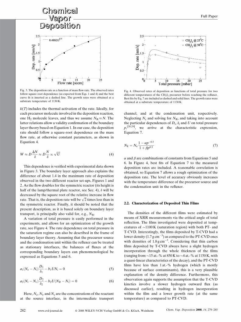
Fig. 3. The deposition rate as a function of mass flow rate. The observed rates
follow square root dependence (as expected from Eqs. 1 and 4) and the best
curve fit is inserted as a dashed line. The growth rates were obtained at a
substrate temperature of 1130K.
k(T) includes the thermal activation of the rate. Ideally, for
each precursor molecule involved in the deposition reaction,
one H2 molecule leaves, and thus we assume NR�N. The
latter relations allow a validity confirmation of the boundary
layer theory based on Equation 1. In our case, the deposition
rate should follow a square-root dependence on the mass
flow rate, at otherwise constant parameters, as shown in
Equation 4.
W � DDN
d� D
N
d/
ffiffiffiffiffiU
p(4)
This dependence is verified with experimental data shown
in Figure 3. The boundary layer approach also explains the
difference of about 1.4 in the maximum rate of deposition
observed in the two different reactor set-ups, Figures 1 and
2. As the flow doubles for the symmetric reactor (its height is
half of the lamp/thermal plate reactor, see Sec. 4), d will be
decreased by the square root of the relative increase in flow
rate. That is, the deposition rate will beffiffiffi2
ptimes less than in
the symmetric reactor. Finally, it should be noted that the
present description, as it is based solely on boundary layer
transport, is principally also valid for, e.g., NR.
A variation of total pressure is easily performed in the
experiments, and allows for an optimization of the growth
rate, see Figure 4. The rate dependence on total pressure in
the saturation regime can also be described in the frame of
boundary layer theory. Assuming that the precursor source
and the condensation unit within the refluxer can be treated
as stationary interfaces, the balances of fluxes at the
corresponding boundary layers can phenomenological be
expressed as Equations 5 and 6.
a1 Ne �Nið ÞD1
d1� b1UNi ¼ 0 (5)
a2 Ni �Ncð ÞD2 � b2U NR �Nið Þ ¼ 0 (6)
d2Here,Ne,Ni, andNc are the concentrations of the reactant
at the source interface, in the intermediate transport
282 www.cvd-journal.de � 2008 WILEY-VCH Verlag GmbH &
channel, and at the condensation unit, respectively.
Neglecting Nc and solving for NR, and taking into account
the particular dependences of Di, di and U on total pressure
p,[28,29], we arrive at the characteristic expression,
Equation 7.
NR ¼ Ne1� ap�0:5
1þ bp0:5(7)
a and b are combinations of constants from Equations 5 and
6. In Figure 4, best fits of Equation 7 to the measured
deposition rates are included. A reasonable correlation is
obtained, so Equation 7 allows a rough optimization of the
deposition rate. The level of accuracy obviously increases
with the temperature difference of the precursor source and
the condensation unit in the refluxer.
2.2. Characterization of Deposited Thin Films
The densities of the different films were estimated by
means of XRR measurements via the critical angle of total
reflection. The films investigated were deposited at temp-
eratures of �1100K (saturation region) with both PT- and
T-CVD. Interestingly, the films deposited by T-CVD had a
lower density (1.7 g cm�3) as compared to the PT-CVD ones
with densities of 1.8 g cm�3. Considering that thin carbon
films deposited by T-CVD always have a slight hydrogen
incorporation through the whole thickness of the films
(ranging from�15 at.-% at 850K to�4 at.-% at 1150K, with
a quasi-linear characteristics of the decay), and the PT-CVD
films have less than 1 at.-% hydrogen (which is mostly
because of surface contaminants), this is a very plausible
explanation of the density difference. Furthermore, this
observation again supports the assumption that the T-CVD
kinetics involve a slower hydrogen outward flux (as
discussed earlier), resulting in hydrogen incorporation
within the film and a lower growth rate (at the same
temperature) as compared to PT-CVD.
Co. KGaA, Weinheim Chem. Vap. Deposition 2008, 14, 279–285
Full Paper
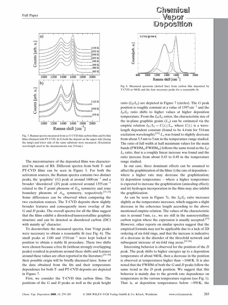
Fig. 5. Raman spectra measured from a) T-CVD thin carbon films and b) thin
films obtained with PT-CVD. In b) both the deposit on the upper side (facing
the lamp) and lower side of the same substrate were measured. (Excitation
wavelength used in the measurements was 514 nm.)
Fig. 6. Measured spectrum (dotted line) from carbon film deposited by
T-CVD at 940K and the four necessary peaks for a reasonable fit.
The microstructure of the deposited films was character-
ized by means of RS. Different spectra from both T- and
PT-CVD films can be seen in Figure 5. For both the
activation sources, the Raman spectra contains two distinct
peaks, the ‘graphitic’ (G) peak at around 1600 cm�1 and a
broader ‘disordered’ (D) peak centered around 1355 cm�1
related to the G point phonons of E2g symmetry and zone
boundary phonons of A1g symmetry, respectively.[31,32]
Some differences can be observed when comparing the
two excitation sources. The T-CVD deposits show slightly
broader features and consequently more overlap of the
G and D peaks. The overall spectra for all the films suggest
that the films exhibit a disordered/nanocrystalline graphitic
structure and can be denoted as disordered carbon (DC)
with mainly sp2 character.
To deconvolute the measured spectra, four Voigt peaks
were necessary to obtain a reasonable fit (see Fig. 6). The
small peaks at 1180 and 1510 cm�1 were kept locked in
position to obtain a stable fit procedure. These two shifts
were chosen because a free fit (without strongly overlapping
peaks) resulted in positions around these shifts and features
around these values are often reported in the literature;[33–36]
their possible origin will be briefly discussed later. Some of
the data obtained from the fits and their temperature
dependence for both T- and PT-CVD deposits are depicted
in Figure 7.
First, we consider the T-CVD thin carbon films. The
positions of the G and D peaks as well as the peak height
Chem. Vap. Deposition 2008, 14, 279–285 � 2008 WILEY-VCH Verlag G
ratio (ID/IG) are depicted in Figure 7 (circles). The G peak
position is roughly constant at a value of 1597 cm�1 and the
ID/IG ratio shifts to higher values at higher deposition
temperature. From the ID/IG ratios, the characteristic size of
the in-plane graphitic grains (La) can be estimated via the
empiric relation ID=IG ¼ CðlÞ=La, where CðlÞ is a wave-
length dependent constant (found to be 4.4 nm for 514 nm
excitation wavelength).[31] La was found to slightly decrease
from about 5.5 nm to 5 nm in the temperature range studied.
The ratio of full width at half maximum values for the main
bands (FWHMG/FWHMD) follows the same trend as the ID/
IG ratio, that is a roughly linear increase was found and the
ratio increase from about 0.43 to 0.49 in the temperature
range studied.
In our case, three dominant effects can be assumed to
affect the graphitization of the films: i) the rate of deposition –
where a higher rate may decrease the graphitization;
ii) deposition temperature – where a higher temperature
is expected to increase the graphitization (annealing effect);
and iii) hydrogen incorporation in the films may also inhibit
the graphitization.
As can be seen in Figure 7c, the ID/IG ratio increases
slightly as the temperature increases, which suggests a slight
decrease in the coherence length according to the above
mentioned empiric relation. The values of the characteristic
size is around 5 nm, i.e., we are still in the nanocrystalline
carbon region where the expression is usually accepted.[37]
However, other reports on similar spectra suggest that the
empirical formula may not be applicable due to a lack of 2D
ordering of six-fold rings, and that the increase is indicative
of a decrease in the disorder of the threefold network and
subsequent increase of six-fold ring areas.[35,36]
Interesting behavior is observed for the position of the D
peak. The peak shifts to higher energies up to a deposition
temperature of about 940K, then a decrease in the position
is observed at temperatures higher than �1040K. It is also
noted that the FWHM of both theG andD peaks follow the
same trend as the D peak position. We suggest that this
behavior is mainly due to the growth rate dependence on
temperature in the various temperature regions (see Fig. 1).
That is, at deposition temperatures below �950K, the
mbH & Co. KGaA, Weinheim www.cvd-journal.de 283
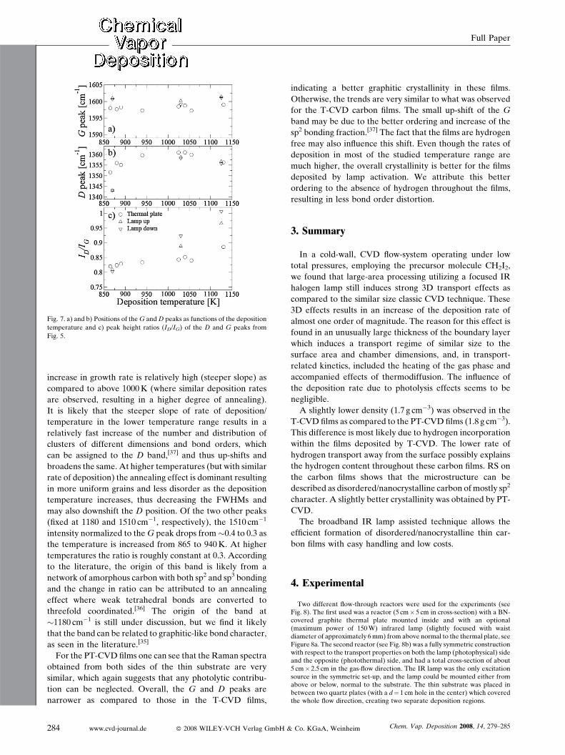
Full Paper
Fig. 7. a) and b) Positions of theG andD peaks as functions of the deposition
temperature and c) peak height ratios (ID/IG) of the D and G peaks from
Fig. 5.
increase in growth rate is relatively high (steeper slope) as
compared to above 1000K (where similar deposition rates
are observed, resulting in a higher degree of annealing).
It is likely that the steeper slope of rate of deposition/
temperature in the lower temperature range results in a
relatively fast increase of the number and distribution of
clusters of different dimensions and bond orders, which
can be assigned to the D band,[37] and thus up-shifts and
broadens the same. At higher temperatures (but with similar
rate of deposition) the annealing effect is dominant resulting
in more uniform grains and less disorder as the deposition
temperature increases, thus decreasing the FWHMs and
may also downshift the D position. Of the two other peaks
(fixed at 1180 and 1510 cm�1, respectively), the 1510 cm�1
intensity normalized to theG peak drops from�0.4 to 0.3 as
the temperature is increased from 865 to 940K. At higher
temperatures the ratio is roughly constant at 0.3. According
to the literature, the origin of this band is likely from a
network of amorphous carbon with both sp2 and sp3 bonding
and the change in ratio can be attributed to an annealing
effect where weak tetrahedral bonds are converted to
threefold coordinated.[36] The origin of the band at
�1180 cm�1 is still under discussion, but we find it likely
that the band can be related to graphitic-like bond character,
as seen in the literature.[35]
For the PT-CVDfilms one can see that the Raman spectra
obtained from both sides of the thin substrate are very
similar, which again suggests that any photolytic contribu-
tion can be neglected. Overall, the G and D peaks are
narrower as compared to those in the T-CVD films,
284 www.cvd-journal.de � 2008 WILEY-VCH Verlag GmbH &
indicating a better graphitic crystallinity in these films.
Otherwise, the trends are very similar to what was observed
for the T-CVD carbon films. The small up-shift of the G
band may be due to the better ordering and increase of the
sp2 bonding fraction.[37] The fact that the films are hydrogen
free may also influence this shift. Even though the rates of
deposition in most of the studied temperature range are
much higher, the overall crystallinity is better for the films
deposited by lamp activation. We attribute this better
ordering to the absence of hydrogen throughout the films,
resulting in less bond order distortion.
3. Summary
In a cold-wall, CVD flow-system operating under low
total pressures, employing the precursor molecule CH2I2,
we found that large-area processing utilizing a focused IR
halogen lamp still induces strong 3D transport effects as
compared to the similar size classic CVD technique. These
3D effects results in an increase of the deposition rate of
almost one order of magnitude. The reason for this effect is
found in an unusually large thickness of the boundary layer
which induces a transport regime of similar size to the
surface area and chamber dimensions, and, in transport-
related kinetics, included the heating of the gas phase and
accompanied effects of thermodiffusion. The influence of
the deposition rate due to photolysis effects seems to be
negligible.
A slightly lower density (1.7 g cm�3) was observed in the
T-CVD films as compared to the PT-CVDfilms (1.8 g cm�3).
This difference is most likely due to hydrogen incorporation
within the films deposited by T-CVD. The lower rate of
hydrogen transport away from the surface possibly explains
the hydrogen content throughout these carbon films. RS on
the carbon films shows that the microstructure can be
described as disordered/nanocrystalline carbon ofmostly sp2
character. A slightly better crystallinity was obtained by PT-
CVD.
The broadband IR lamp assisted technique allows the
efficient formation of disordered/nanocrystalline thin car-
bon films with easy handling and low costs.
4. Experimental
Two different flow-through reactors were used for the experiments (seeFig. 8). The first used was a reactor (5 cm� 5 cm in cross-section) with a BN-covered graphite thermal plate mounted inside and with an optional(maximum power of 150W) infrared lamp (slightly focused with waistdiameter of approximately 6mm) from above normal to the thermal plate, seeFigure 8a. The second reactor (see Fig. 8b) was a fully symmetric constructionwith respect to the transport properties on both the lamp (photophysical) sideand the opposite (photothermal) side, and had a total cross-section of about5 cm� 2.5 cm in the gas-flow direction. The IR lamp was the only excitationsource in the symmetric set-up, and the lamp could be mounted either fromabove or below, normal to the substrate. The thin substrate was placed inbetween two quartz plates (with a d¼ 1 cm hole in the center) which coveredthe whole flow direction, creating two separate deposition regions.
Co. KGaA, Weinheim Chem. Vap. Deposition 2008, 14, 279–285
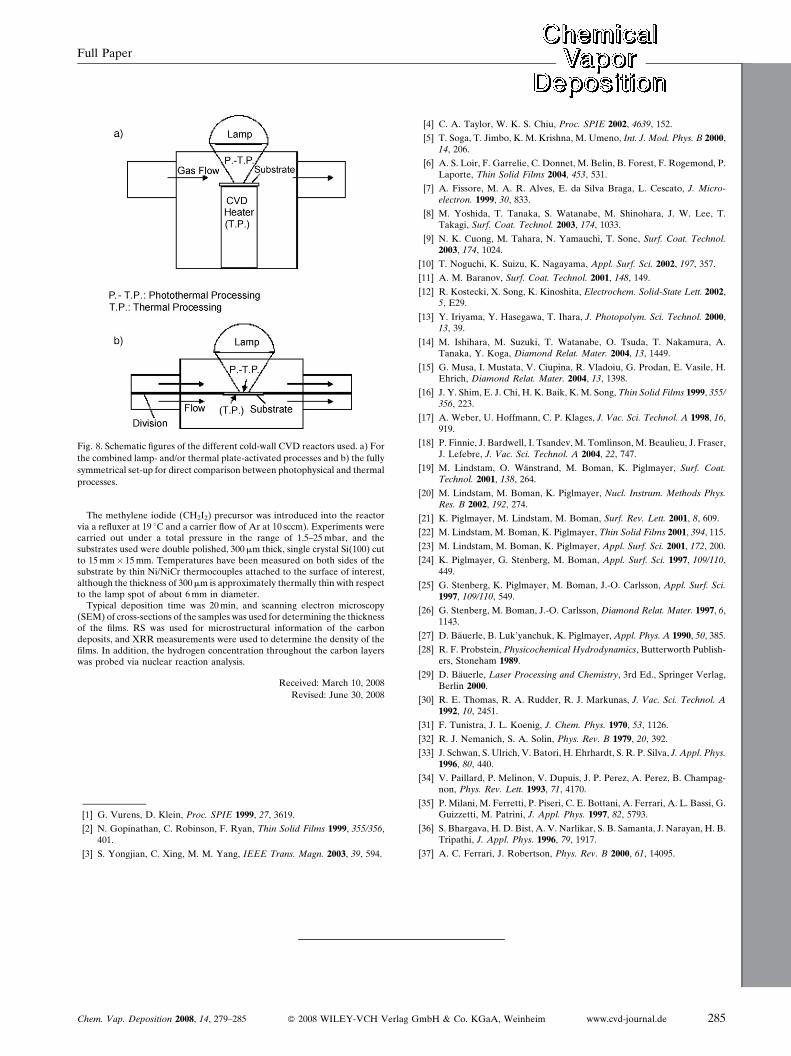
Full Paper
Fig. 8. Schematic figures of the different cold-wall CVD reactors used. a) For
the combined lamp- and/or thermal plate-activated processes and b) the fully
symmetrical set-up for direct comparison between photophysical and thermal
processes.
The methylene iodide (CH2I2) precursor was introduced into the reactorvia a refluxer at 19 8C and a carrier flow of Ar at 10 sccm). Experiments werecarried out under a total pressure in the range of 1.5–25mbar, and thesubstrates used were double polished, 300mm thick, single crystal Si(100) cutto 15mm� 15mm. Temperatures have been measured on both sides of thesubstrate by thin Ni/NiCr thermocouples attached to the surface of interest,although the thickness of 300mm is approximately thermally thin with respectto the lamp spot of about 6mm in diameter.Typical deposition time was 20min, and scanning electron microscopy
(SEM) of cross-sections of the samples was used for determining the thicknessof the films. RS was used for microstructural information of the carbondeposits, and XRR measurements were used to determine the density of thefilms. In addition, the hydrogen concentration throughout the carbon layerswas probed via nuclear reaction analysis.
Received: March 10, 2008
Revised: June 30, 2008
[1] G. Vurens, D. Klein, Proc. SPIE 1999, 27, 3619.
[2] N. Gopinathan, C. Robinson, F. Ryan, Thin Solid Films 1999, 355/356,401.
[3] S. Yongjian, C. Xing, M. M. Yang, IEEE Trans. Magn. 2003, 39, 594.
Chem. Vap. Deposition 2008, 14, 279–285 � 2008 WILEY-VCH Verlag G
[4] C. A. Taylor, W. K. S. Chiu, Proc. SPIE 2002, 4639, 152.
[5] T. Soga, T. Jimbo, K. M. Krishna, M. Umeno, Int. J. Mod. Phys. B 2000,14, 206.
[6] A. S. Loir, F. Garrelie, C. Donnet, M. Belin, B. Forest, F. Rogemond, P.Laporte, Thin Solid Films 2004, 453, 531.
[7] A. Fissore, M. A. R. Alves, E. da Silva Braga, L. Cescato, J. Micro-electron. 1999, 30, 833.
[8] M. Yoshida, T. Tanaka, S. Watanabe, M. Shinohara, J. W. Lee, T.Takagi, Surf. Coat. Technol. 2003, 174, 1033.
[9] N. K. Cuong, M. Tahara, N. Yamauchi, T. Sone, Surf. Coat. Technol.2003, 174, 1024.
[10] T. Noguchi, K. Suizu, K. Nagayama, Appl. Surf. Sci. 2002, 197, 357.
[11] A. M. Baranov, Surf. Coat. Technol. 2001, 148, 149.
[12] R. Kostecki, X. Song, K. Kinoshita, Electrochem. Solid-State Lett. 2002,5, E29.
[13] Y. Iriyama, Y. Hasegawa, T. Ihara, J. Photopolym. Sci. Technol. 2000,13, 39.
[14] M. Ishihara, M. Suzuki, T. Watanabe, O. Tsuda, T. Nakamura, A.Tanaka, Y. Koga, Diamond Relat. Mater. 2004, 13, 1449.
[15] G. Musa, I. Mustata, V. Ciupina, R. Vladoiu, G. Prodan, E. Vasile, H.Ehrich, Diamond Relat. Mater. 2004, 13, 1398.
[16] J. Y. Shim, E. J. Chi, H. K. Baik, K. M. Song, Thin Solid Films 1999, 355/356, 223.
[17] A. Weber, U. Hoffmann, C. P. Klages, J. Vac. Sci. Technol. A 1998, 16,919.
[18] P. Finnie, J. Bardwell, I. Tsandev, M. Tomlinson, M. Beaulieu, J. Fraser,J. Lefebre, J. Vac. Sci. Technol. A 2004, 22, 747.
[19] M. Lindstam, O. Wanstrand, M. Boman, K. Piglmayer, Surf. Coat.Technol. 2001, 138, 264.
[20] M. Lindstam, M. Boman, K. Piglmayer, Nucl. Instrum. Methods Phys.Res. B 2002, 192, 274.
[21] K. Piglmayer, M. Lindstam, M. Boman, Surf. Rev. Lett. 2001, 8, 609.
[22] M. Lindstam, M. Boman, K. Piglmayer, Thin Solid Films 2001, 394, 115.
[23] M. Lindstam, M. Boman, K. Piglmayer, Appl. Surf. Sci. 2001, 172, 200.
[24] K. Piglmayer, G. Stenberg, M. Boman, Appl. Surf. Sci. 1997, 109/110,449.
[25] G. Stenberg, K. Piglmayer, M. Boman, J.-O. Carlsson, Appl. Surf. Sci.1997, 109/110, 549.
[26] G. Stenberg, M. Boman, J.-O. Carlsson, Diamond Relat. Mater. 1997, 6,1143.
[27] D. Bauerle, B. Luk’yanchuk, K. Piglmayer, Appl. Phys. A 1990, 50, 385.
[28] R. F. Probstein, Physicochemical Hydrodynamics, Butterworth Publish-ers, Stoneham 1989.
[29] D. Bauerle, Laser Processing and Chemistry, 3rd Ed., Springer Verlag,Berlin 2000.
[30] R. E. Thomas, R. A. Rudder, R. J. Markunas, J. Vac. Sci. Technol. A1992, 10, 2451.
[31] F. Tunistra, J. L. Koenig, J. Chem. Phys. 1970, 53, 1126.
[32] R. J. Nemanich, S. A. Solin, Phys. Rev. B 1979, 20, 392.
[33] J. Schwan, S. Ulrich, V. Batori, H. Ehrhardt, S. R. P. Silva, J. Appl. Phys.1996, 80, 440.
[34] V. Paillard, P. Melinon, V. Dupuis, J. P. Perez, A. Perez, B. Champag-non, Phys. Rev. Lett. 1993, 71, 4170.
[35] P. Milani, M. Ferretti, P. Piseri, C. E. Bottani, A. Ferrari, A. L. Bassi, G.Guizzetti, M. Patrini, J. Appl. Phys. 1997, 82, 5793.
[36] S. Bhargava, H. D. Bist, A. V. Narlikar, S. B. Samanta, J. Narayan, H. B.Tripathi, J. Appl. Phys. 1996, 79, 1917.
[37] A. C. Ferrari, J. Robertson, Phys. Rev. B 2000, 61, 14095.
mbH & Co. KGaA, Weinheim www.cvd-journal.de 285