Photonic logic-gates - RiuNet - Universidad Polit©cnica de Valencia
171
Photonic logic-gates: boosting all-optical header processing in future packet-switched networks Jose M. Martínez Canet December 2006
Transcript of Photonic logic-gates - RiuNet - Universidad Polit©cnica de Valencia

Photonic logic-gates: boosting all-optical header processing in future packet-switched networks
Jose M. Martínez Canet
December 2006


To the memory of my grandma
A la meua iaia
To my familiy
A la meua família

i
Table of contents
Abstract v
Resum vii
Resumen iv
Acknowledgments xi
1. Introduction 1.1. Rationale .................................................................................................. 1 1.1.1. The LASAGNE project ............................................................... 2 1.1.2. Header processing ..................................................................... 6 1.2. Thesis objectives ...................................................................................... 7 1.3. Outline of this work ................................................................................... 8 1.4. References ............................................................................................... 10
2. Architectures and technologies to implement all-optical logic gates: state
of the art
2.1. Introduction ............................................................................................... 13 2.2. Architectures for all-optical logic gates ..................................................... 14 2.2.1. SAGNAC interferometers ........................................................... 16 2.2.2. The Ultrafast Nonlinear Interferometer (UNI) ............................. 23 2.2.3. Logic gates based on nonlinearities on SOAs ........................... 24 2.2.4. The SOA based Mach-Zehnder Interferometer ......................... 27 2.3. Summary and conclusions ....................................................................... 30 2.4. References ............................................................................................... 32
ii
3. Optical logic gates based on SOA-MZI 3.1. Introduction ............................................................................................... 41 3.2. Interferometry ........................................................................................... 42 3.3. All-optical logic gates employing the SOA-MZI ........................................ 45 3.3.1. XOR ........................................................................................... 45 3.3.2. AND ............................................................................................ 57 3.3.3. OR .............................................................................................. 60 3.3.4. NOT ............................................................................................ 65 3.4. Summary and conclusions ....................................................................... 68 3.5. References ............................................................................................... 70
4. Optical correlator (I): Configuration based on cascaded SOA-MZIs 4.1. Introduction ............................................................................................... 73 4.2. Simulation study ....................................................................................... 75 4.2.1. Architecture and principle of operation ....................................... 75 4.2.2 Simulation results ....................................................................... 77 4.3. Experimental validation ............................................................................ 78 4.3.1. Set-up for two-bit correlator ........................................................ 78 4.3.2. Experimental results ................................................................... 80 4.4. Summary and conclusions ....................................................................... 83 4.5. References ............................................................................................... 84
5. Optical correlator (II): N-bit logic XOR gate with feedback 5.1. Introduction ............................................................................................... 87 5.2. Simulation study ....................................................................................... 88 5.2.1. Principle of operation ................................................................. 88 5.2.2. Proposed architecture ................................................................ 89 5.2.3. Simulation results ....................................................................... 92 5.3 Experimental validation ………………………………………………………. 98 5.3.1. Set-up for two-bit correlator ……………………………………….. 98 5.3.2. Principle of operation ………………………………………………. 99 5.4. Design of a mask layout for a PIC ............................................................ 102 5.4.1. ePIXnet ...................................................................................... 102 5.4.2. Design of the mask layout .......................................................... 102 5.4. Summary and conclusions ....................................................................... 105 5.5. References ............................................................................................... 107

iii
6. Applications of all-optical logic gates in practical scenarios 6.1. Introduction ............................................................................................... 109 6.2 All-optical packet routing scheme based on SOA-MZIs: a first approach 110 6.2.1. All-optical packet router architecture .......................................... 110 6.2.2. Simulation results of all-optical packet routing ........................... 113 6.3. All-optical label processing and forwarding in the frame of LASAGNE
project ....................................................................................................... 116 6.3.1. All-optical routing concept .......................................................... 117 6.3.2. Implementation of sub-systems ................................................. 119 6.3.3. Experimental results ................................................................... 120 6.4. Multilogic project: an overview .................................................................. 123 6.4.1. Design of a multi-function photonic device for optical
computing ................................................................................... 124 6.5. Summary and conclusions ....................................................................... 125 6.6. References ............................................................................................... 126
7. Summary and conclusions 7.1. Summary and conclusions ....................................................................... 129 7.2. Future research ........................................................................................ 132 7.3. References ............................................................................................... 134
Appendix A. List of Ph.D. publications 136
Appendix B. Boolean Truth Tables 141
List of acronyms 147
List of figures 151
List of tables 155

iv

v
Abstract
Optical packet networks topic has attracted very interest within the last years. Several efforts have been addressed to deal with all those issues derived from the use of optical packets to carry the information. Header processing is one of the main functionalities required at intermediate nodes, where a packet must be routed to the corresponding destination. All-optical techniques for address recognition and routing are expected to reduce the processing delays compared to electronic processing, therefore decreasing the latency of the communications link. Optical header recognition can be achieved using several different optical data processing methods. The aim of this work is the proposal of new architectures for header processing based on the use of all-optical logical gates. These architectures are implemented based on the semiconductor optical amplifier Mach-Zehnder Interferometer (SOA-MZI) as a key element, using the cross-phase modulation (XPM) nonlinear effect in SOAs to achieve the required functionality. The SOA-MZI structure using XPM turns out as a very promising candidate because of its advantages of low energy requirements, compactness, high extinction ratio (ER), regenerative capability and low chirp. The work presented in this Thesis has been focused on the XOR logic gate implementation, since it is a very versatile approach for implementing many functions in optical networks. Two schemes for all-optical packet header recognition are proposed based on the XOR logic gate. The first proposed scheme is based on cascaded SOA-MZIs, which provides potentiality to build a fully photonic-integrated circuit. The second approach proposed in this Thesis to perform packet header processing solves the scalability issue by adding to the SOA-MZI an external feedback loop. Furthermore, some applications for header processing and routing are presented in this Thesis based on the XOR logic gate optical correlator. A novel architecture for all-optical label reading and packet routing are studied. The implementation of these functionalities using all-optical network sub-systems are demonstrated by functional interconnection of SOA-MZI based integrated devices.


vii
Resum
Les xarxes òptiques de paquets s’han convertit en els darrers anys en un dels temes de rereguarda en el camp de les tecnologies de comunicacions. El processament de capçaleres és una de les funcions més importants que es duen a terme en els nodes intermedis, on un paquet ha de ser encaminat a la seua destinació corresponent. L’ús de tecnologia completament òptica per la implementació de les funcions d’encaminament i reconeixement de capçaleres redueix el retard de processament respecte a aquell del processat elèctric, disminuint així la latència a l’enllaç de comunicacions. Existeixen diferents mètodes de processament de dades per implementar el reconeixement de capçaleres. L’objectiu d’aquest treball és la proposta de noves arquitectures per el processament de capçaleres basat en l’ús de portes lògiques completament òptiques. Aquestes arquitectures tenen com element clau l’interferòmetre Mach-Zehnder implementat amb l’amplificador òptic de semiconductor (SOA-MZI), i utilitzen l’efecte no lineal de modulació creuada de fase (XPM) en els SOAs per tal de realitzar aquesta funcionalitat. L’estructura SOA-MZI amb XPM és una de les alternatives més atractives per els nombrosos avantatges que presenta, com per exemple els requisits de baixa energia pels senyals d’entrada, el seu disseny compacte, una elevada relació d’extinció (ER), regeneració del senyal i baix nivell de chirp que introdueixen. Aquest treball s’ha centrat en la implementació de la funcionalitat lògica XOR. Mitjançant aquesta funció es poden realitzar diverses funcionalitats en les xarxes òptiques. Es proposen dos esquemes per el reconeixement de capçaleres basat en l’ús de la porta XOR. El primer esquema utilitza portes en cascada. El segon esquema presenta una arquitectura molt escalable, i es basa en l’ús d’un bucle de realimentació implementat al port d’eixida de la porta. Tanmateix, també es presenten algunes aplicacions del processament de capçaleres per l’encaminament de paquets basats en l’ús del correlador òptic amb la porta XOR. Es demostra la implementació d’aquestes funcionalitats utilitzant sub-sistemes completament òptics mitjançant la interconnexió de dispositius basats en SOA-MZIs.


ix
Resumen
Las redes ópticas de paquetes se han convertido en los últimos años en uno de los temas de vanguardia en el campo de las tecnologías de comunicaciones. El procesado de cabeceras es una de las funciones más importantes que se llevan a cabo en nodos intermedios, donde un paquete debe ser encaminado a su destino correspondiente. El uso de tecnología completamente óptica para las funciones de encaminamiento y reconocimiento de cabeceras reduce el retardo de procesado respecto al procesado eléctrico, disminuyendo de ese modo la latencia en el enlace de comunicaciones. Existen diferentes métodos de procesado de datos para implementar el reconocimiento de cabeceras. El objetivo de este trabajo es la propuesta de una nueva arquitectura para el procesado de cabeceras basado en el uso de puertas lógicas completamente ópticas. Estas arquitecturas tienen como elemento clave el interferómetro Mach-Zehnder basado en el amplificador óptico de semiconductor (SOA-MZI), y utilizan el efecto no lineal de modulación cruzada de fase (XPM) en los SOAs para realizar dicha funcionalidad. La estructura SOA-MZI con XPM es una de las alternativas más atractivas debido a las numerosas ventajas que presenta, como por ejemplo los requisitos de baja energía para las señales de entrada, su diseño compacto, una elevada relación de extinción (ER), regeneración de la señal y el bajo nivel de chirp que introducen. Este trabajo se ha centrado en la implementación de la funcionalidad lógica XOR. Mediante esta función se pueden realizar diversas funcionalidades en las redes ópticas. Se proponen dos esquemas para el reconocimiento de cabeceras basados en el uso de la puerta XOR. El primer esquema utiliza puertas en cascada. El segundo esquema presenta una arquitectura muy escalable, y se basa en el uso de un bucle de realimentación implementado a la salida de la puerta. Asimismo, también se presentan algunas aplicaciones del procesado de cabeceras para el encaminamiento de paquetes basadas en el uso del correlador óptico con la puerta XOR. Se demuestra la implementación de estas funcionalidades utilizando sub-sistemas completamente ópticos mediante la interconexión de dispositivos integrados basados en SOA-MZIs.


xi
Acknowledgments
I would like to express my gratitude to Professor Javier Martí, for giving me the opportunity to be a member of his research group. I am indebted to him for the knowledge I have gained in the areas of Photonics during my five years at the FRG/NTC group. I am extremely grateful to Prof. Francisco Ramos (for me, always Paco) for his constant encouragement and support. I will forever remain indebted to him for being my mentor and for taking an active interest in the progress of my thesis. I would like to acknowledge all the members of the NTC group (those that are currently enrolled and those who are not here) for making my stay at UPVLC more enjoyable. I think it is not fair to name only some of them, because from everyone I got something. I wish all the best to all of them. I would like to thank the Universitat Politécnica de València for supporting my graduate studies for four years. During the realisation of this Thesis I have acquired a lot of professional skills, knowledge and experience. But what I really learned is that I have a light that will never fade: my family. My deepest thanks, of course, go to my parents (Filo and Jose), my sisters (Ana and Maria Jose) and my brother (Davit) for their unconditional support, patience and encouragement not only in my professional work, but in my private life. I am really proud of you. Thanks for your light.


1
Chapter 1
Introduction
1.1. Rationale Within today’s Internet, data is transported between powerful electronic Internet protocol (IP) routers using optical-fibre transmission and wavelength-division-multiplexing (WDM) systems. Fibre-transmission systems today typically carry tens of wavelengths modulated at rates beyond 1 Gbit/s. In an IP router, multiple WDM fibres are terminated and signals are converted from the optical to the electronic domain at the input and from electronic to optical at the output. Today’s routers need to handle in excess of 1 Tbit/s of data in order to redirect incoming Internet packets from fully loaded WDM fibres. When comparing the increase of optical fibres capacity with the speed of electronic processor, it arises that there is a potential mismatch in bandwidth handling capability between fibre-transmission systems and electronic routers. This situation could become more complicated if we consider that future routers will terminate potentially hundreds or thousands of optical wavelengths and the increase in bit rate per wavelength will head out to 40 Gbit/s and potentially beyond. Electronic processing in this scenario would not be able to handle the routing of a massive number of packets per second, which could easily lead to router congestion. Or at least, not a reasonable cost. From an economic perspective, conversions between optical and electrical formats at the inputs and outputs of a router can grow to be half of the cost of a node. And even more, electronics working at high bit rates would show up a problem of power consumption and heat dissipation. The eventual goal is to reduce the amount of complex electronics, and thus, the cost, by migrating to an all-optical network, where data is switched and routed transparently in optical form, with a minimum amount of electronic processing. Thereby, all-optical processing appears to be a solution to avoid the bottleneck imposed by the nodes based on electronic processing. However, the photonic technology is not mature enough to support all the functionalities on the node in an all-optical way.

Chapter 1: Introduction
2
At this point, the concept of all-optical label swapping (AOLS) has been proposed as a viable approach towards resolving the mismatch between fibre transmission capacity and router packet forwarding capacity [blu00]. In such an AOLS scenario, all packet-by-packet routing and forwarding functions of multi-protocol label swapping (MPLS) are implemented directly in the optical domain. By using optical labels the IP packets are directed through the core optical network without requiring O/E/O conversions whenever a routing decision is necessary. The main advantage of this approach is the ability to route packets/bursts independently of bit rate, packet format and packet length. This increases the network flexibility and granularity, which become highly desirable attributes in broadband networks characterized by bandwidth-on-demand applications. In addition, compared to previous node implementations [vla03, cap03, dit03], the all-optical network node must be capable of operating with in-band serial-bit label signalling at the line-rate, attaining high bandwidth utilization and simplified transmitter implementation. The ability to process labels at the line-rate through all-optical techniques eliminates the need for O/E/O conversions and allows for high information capacity to be encapsulated in the labels compared to lower-bit rate approaches [blu00]. Further, the labels are generated with the same light sources and intensity modulators as the payload [mor03], a major requirement for implementation of next generation truly all-optical networks. The work presented in this Thesis has been developed within the scope of the IST sixth framework programme LASAGNE1 project, whose basics and aims will be described in the next section. This project is coordinated by the Nanophotonics Technology Center (Universidad Politécnica de Valencia), research group where the author of this Thesis is associated researcher since 2001.
1.1.1. The LASAGNE project
LASAGNE2 proposes a novel node and network architecture based on AOLS scenario. The LASAGNE project aims at designing and implementing the first, modular, scalable and truly all-optical photonic router capable of operating at 40 Gbit/s. LASAGNE objectives include studying, proposing and validating the use of all-optical logic gates based on commercially available technologies to implement network functionalities at the metro/core network nodes in AOLS networks [blu00, cap03, lis00]. The optical logic gates are designed and implemented using the same fundamental building block: the semiconductor optical amplifier (SOA) based Mach-Zehnder interferometer (SOA-MZI), which results in a flexible and scalable approach in terms of manufacturing. Although the photonic prototype is 1 LASAGNE acronym stands for “All-optical LAbel SwApping employing optical logic Gates in NEtwork nodes”. 2 http://www.ist-lasagne.org.

Capítol 1: Introducció
3
currently designed as interconnected fibre-pigtailed SOA-MZI devices, it is envisaged that through the advent of photonic integration research, such a router could be potentially integrated in a single hybrid platform. For instance, IST-MUFINS project3 aims at monolithically integrating arrays of interferometric switches, towards photonic very large scale integration (VLSI). Network Concept An example of an AOLS network is shown in Figure 1-1. The IP packets enter the AOLS network through the ingress node. There these “low-bit rate” packets (~10 Gbit/s) are optically time domain multiplexed to form high-bit rate packets or bursts (~40-80 Gbit/s), encapsulated with an optical label and re-transmitted on a new wavelength if required. Once at the MAN/WAN network, only the optical label is used to make routing decisions at the optical nodes, whereas the wavelength is used to dynamically re-direct (forward) the high-bit rate packets. Each AOLS router uses the information of the extracted labels to perform the routing decision and forward the packets toward the egress edge router. An optical core router performs routing and forwarding operations together with wavelength conversion and label swapping. Throughout this process, the integrity of the high-bit rate packets is maintained in the optical domain.
Input port
Output port
Access Network
Access NetworkOADM
Egress edgerouter with
AOLS interface
Ingress edgerouter with
AOLS interface
AOLSrouter orsubnet
AOLSrouter orsubnet
AOLSrouter orsubnet
AOLSrouter orsubnet
Optical AOLS Metro/Core Network
Optical label and IP data at λi
Optical label and IP data at λj
Optical label
IP packet
OADM
OADM
OADM
OADM
OADM
Figure 1-1. LASAGNE AOLS network scenario.
3 http://mufins.cti.gr/tiki-summary.php.

Chapter 1: Introduction
4
Node Design Figure 1-2 shows a block diagram of the proposed architecture of the node that is designed, studied, simulated and implemented in LASAGNE. To focus on the all-optical functionalities and due to limited resources, the implementation and experimental validation is limited to the all-optical label swapper and packet router detailed in Figure 1-2. The main functionalities required by the AOLS (label reading, new label insertion and wavelength conversion) are based on the use of all-optical logic gates and flip-flops. As it is shown in Figure 1-2, the wavelengths entering the node are first demultiplexed and for each wavelength an AOLS block is implemented. An AOLS block comprehends the true forwarding functionality of incoming packets.
AWG
AWG
AWG2x2
for multicast purposes
add wavelengths drop wavelengths
in fiber #1
wiring matrix
in fiber #2
out fiber #1
out fiber #2
AOLS
AOLS
AOLS
AOLS
AOLS
AOLS
AOLS
AOLS
AOLS
AOLS
AOLS
AOLS
2x2
?1
?2
?3
?4
?1
?2
?3
?4
λ
λ
λ
λ
λ
λ
λ
λ
AWG
AWG
AWG2x2
for multicast purposes
add wavelengths drop wavelengths
in fiber #1
wiring matrix
in fiber #2
out fiber #1
out fiber #2
AOLS
AOLS
AOLS
AOLS
AOLS
AOLS
AOLS
AOLS
AOLS
AOLS
AOLS
AOLS
2x2
?1
?2
?3
?4
?1
?2
?3
?4
λ
λ
λ
λ
λ
λ
λ
λ
Figure 1-2. Proposed photonic routing architecture. Wavelengths entering the node are first demultiplexed and for each wavelength an AOLS block is implemented. The
packet is then sent through an AWG. Therefore, the wavelength on which the packet leaves the AOLS block determines the outgoing port on which the packet leaves the
node.
Entering the AOLS module the packet payload (40 Gbit/s) and label (10 Gbit/s) are separated [bin02], as shown in Figure 1-3. The extracted optical label is fed to a bank of optical correlators based on all-optical logic XOR gates (AOLXGs) [mar02], where the comparison between the label and a set of local addresses is performed. These local addresses are generated using optical delay lines (ODLs). The local address generation

Capítol 1: Introducció
5
block is comprised of a set of interconnected fibre spans, couplers and splitters which generate a bit sequence out from a single pulse. Thus, comparing the incoming label to the local addresses implies that, for each possible incoming label, a separate ODL and a correlator must be included in the AOLS. After comparison, a high intensity pulse will appear at the output of the XOR correlator with the matching address. This pulse feeds a control-block which drives a wavelength converter.
AOLXG
AOLXG
AOLXG
AOLXG
A#1AddressMatch
AW
G
λk
Label/payload
separation
Packet Routing
Optical correlators
Port 1
Port 2
Port 3
Port 4
λk
λk
Delaying of payloadλ2
Labelinsertion
AOFF[λ0, λ1]
Tunablewavelengthconverter
4x1
λk
ODLs
4x4
Switchmatrix
ODLs
Opticalnotch filter
λ0
New-label generation
PacketClock
Recovery
1x3
4x4
Switchmatrix
4x1
1x4
Network control plane (low-speed dynamically reconfigurable)
AOFF[λ0, λ2]
AOFF[λ0, λ3]
AOFF[λ0, λ4]
4x1
reset
set
1x4
1x4
Singlepulse
generation
A#2
A#3
A#4
1
1
2
3
4
2
3
4
AOLXG: All-optical Label XOR GateAOFF: All-optical Flip-FlopODL: Optical Delay LineA#n: Reference address number n
Local address generation
AOLXG
AOLXG
AOLXG
AOLXG
A#1AddressMatch
AW
G
λkλk
Label/payload
separation
Packet Routing
Optical correlators
Port 1
Port 2
Port 3
Port 4
λk
λk
Delaying of payloadλ2λ2
Labelinsertion
AOFF[λ0, λ1]
Tunablewavelengthconverter
4x1
λkλk
ODLs
4x4
Switchmatrix
4x4
Switchmatrix
ODLs
Opticalnotch filter
λ0λ0
New-label generation
PacketClock
Recovery
1x3
4x4
Switchmatrix
4x4
Switchmatrix
4x1
1x4
Network control plane (low-speed dynamically reconfigurable)Network control plane (low-speed dynamically reconfigurable)
AOFF[λ0, λ2]
AOFF[λ0, λ3]
AOFF[λ0, λ4]
4x1
reset
set
1x4
1x4
Singlepulse
generation
A#2
A#3
A#4
1
1
2
3
4
2
3
4
AOLXG: All-optical Label XOR GateAOFF: All-optical Flip-FlopODL: Optical Delay LineA#n: Reference address number n
Local address generation
Figure 1-3. Detailed LASAGNE all-optical label swapper. The payload is delayed to match the new label generated after the complete processing of the incoming packet
label. The packet payload and the new label with are wavelength converted and routed through the AWG.
The control-block is made up of all-optical flip-flops (AOFFs) [dor03]. Depending on the matching address (correlator output pulse), the appropriate flip-flop will emit a CW signal at a certain wavelength. This way the internal wavelength is chosen. At the same time a new label is generated in the appropriate ODL. The new label is inserted in front of the payload and both the payload and the new label are now converted to the wavelength generated by the flip-flop. The packet is then sent through an arrayed waveguide grating (AWG). Therefore, the wavelength on which the packet leaves the AOLS block determines the outgoing port on which the packet leaves the node. Two switches provide the flexibility to configure the labels and wavelengths. The size of the packet router (for example, number of

Chapter 1: Introduction
6
optical correlators and flip-flops) is very dependent on the number of local addresses and header bit length used in the routing table. The AOLS in Figure 1-3 was depicted for the specific case of 4 different locally-generated addresses (2-bit optical labels). Figure 1-4 shows a schematic diagram block of the described AOLS. The synchronization between the optical subsystems employed in the AOLS-routing node and the timing information of the incoming packet is of crucial importance for the proper operation of the node. The AOLS-node requires timing extraction on a packet-by-packet basis and a packet arrival detection scheme. These functionalities are performed by a clock recovery circuit [bin02a] and a single pulse generator. The former is placed at the beginning of the router and it is capable to handle high-bit rate, burst mode optical packets; the latter generates an optical pulse as a packet arrives to the AOLS. Therefore, the switches used for generating the reference addresses and the new label are ruled by a low-speed dynamically controlled network control plane.
Label comparison
Wavelengthconversion
Label generation
Label insertion
Label/payload separation
PayloadLabel
PayloadLabel
Label comparison
Wavelengthconversion
Label generation
Label insertion
Label/payload separation
PayloadLabel
PayloadLabel
Figure 1-4. Schematic block diagram of the all-optical routing node (AOLS module).The main functionalities are: label/payload separation, label comparison, label generation,
label insertion and wavelength conversion.
1.1.2. Header processing
One of the most significant functionalities in future optical packet networks is header processing. There are different architectures suitable to perform header processing functions. Specifically two approaches are used to implement this functionality: optical correlators and all-optical logic gates. Optical correlators [hun99, sri01, cal01] show good performance in terms of quality. However, O/E conversions are required to process the signal, using some electronic circuitry to process several bits simultaneously [car00]. These O/E conversions are not desirable to allow high bit rates operation. Even for bit rates around 40 Gbit/s these architectures are not advisable for header processing. On the other hand, optical gates can be fully implemented in the optical domain. Furthermore, some

Capítol 1: Introducció
7
configurations have some additional advantages with regard to optical correlators: operation with low signal power levels, high system bit rate operation and polarization independency. Up to now, most of the proposed architectures for header processing are based on optical logic gates, whose logical function is shown in Appendix B. In fact, logic gates make feasible to perform many operations in optical time-division multiplexing (OTDM) networks, such as bit-sequences comparison [ham02], header processing [mar02], parity checking [pou99], labelling of packets [fje01], random bit-sequence generation [hal96, pou99a], binary adders [pou99b], comparator circuits [hou99] or encryptation issues. This versatility is the reason why optical gates are considered to represent the key element in the new age for the OTDM networks. Despite, these architectures were originally thought for switching and demultiplexing functions. Nevertheless, with slight modifications, such as introducing the bit-sequences to compare in the control and data input ports, Boolean functionalities (e.g. XOR) can be achieved. Ultra-high speed address recognition can be performed with all-optical AND or XOR logic gates. Previous researches showed a 6-bit pattern matching AND gate using four-wave mixing (FWM) in a semiconductor diode amplifier [cot95]. However, using an AND gate to match patterns limits the available addresses to a fixed set of keywords since some words can be matched by patterns other than their logical complement [cot93]. As an alternative, all-optical XOR gates overcome the limitation on the available number of keywords or addresses.
1.2. Thesis objectives The aim of this Thesis is the proposal, study, and validation of all-optical logic gates architectures, based on SOA-MZIs. This topic has attracted very interest in the literature in the last years, as can be inferred from the huge number of publications in this field. For example those published by Bintjas and Houbavlis [bin00, hou99] are based on the use of nonlinear elements and fibre. However, the use of fibre makes the scheme difficult to integrate, a key issue on the development of optical devices. Other publications made use of opto-electronic processing [lux96], and can not be considered as all-optical approaches. And on the other side, the key element of the structure presented in this work, i.e. the SOA, is a very versatile element which shows many advantages over other technologies, as for example, easy of integration, high nonlinear effects, low insertion loss, high on/off ratio, etc. The main objectives addressed in this Thesis are as follows:
• The development and study of a novel architecture based on cascaded SOA-MZIs to all-optically perform the logic XOR operation between two input binary sequences.

Chapter 1: Introduction
8
• The development and study of a novel architecture based on a SOA-MZI with feedback to all-optically perform the logic XOR operation between two input binary sequences.
• The experimental implementation and operation demonstration of the all-optical XOR logic gates at 10 Gbit/s.
• The application of the developed XOR logic-gate architectures for header processing in all-optical packet switching network nodes
• The extension and study of the SOA-MZI based logic-gate devices to perform other functions, such AND, OR, and NOT, with minor changes in the initial architecture.
1.3. Outline of this work The content of this Thesis is organised in 7 chapters. In chapter 2, an overview in the state-of-the-art of the different techniques to implement logical functionalities is presented. Previous architectures were based on fibre, which showed its difficulty to be integrated as the main drawback. New configurations based in SOAs emerged to overcome the integration problems. However, SOAs are limited in bit rate operation due to the slow carrier recovery time. This limitation was partially solved by using interferometric arrangements, as for example the SOA-MZI. In chapter 3, optical logic gates based on SOA-MZI structures will be studied. Cross-Phase Modulation (XPM) in SOA-MZIs is the most promising candidate to implement the XOR logic gate because of its attractive features. Furthermore, the use of SOA-MZI as basic building block to implement many other subsystems within a photonic router makes this approach a versatile choice. Chapter 4 presents a logic-gate based architecture which acts as an all-optical packet header processor or optical correlator. The system uses cascaded SOA-MZIs, and shows good performance for 2-bits labels comparison. The mayor drawback of this approach is that, as the number of bits in the label increases, the number of cascaded SOA-MZIs required to perform the optical correlation is higher, and so do the final size and complexity. To overcome the weakness of this architecture regarding scalability, an additional scheme is proposed and studied in chapter 5. This alternative performs the comparison between two sequences using a single device independently of the number of the bits to be compared. It is based on a SOA-MZI XOR logic gate with feedback. Simulations as well as experimental results are presented in this chapter. Optical logic gates have an important impact in practical applications on packet networks. Chapter 6 presents a novel architecture to perform label reading and packet routing all-optically based on XOR logic gates and flip-flops. Furthermore, this chapter gives an

Capítol 1: Introducció
9
overview on the Multilogic project, which can be considered as a preliminary approach to photonic computing. Finally, conclusions and future work are addressed in chapter 7.

Chapter 1: Introduction
10
1.4. References [bin00] C. Bintjas, M. Kalyvas, G. Theophilopoulos, T. Stathopoulos, L. Occhi, L.Schares, G.
Guekos, S. Hansmann, and R. Dall’Ara, "20 Gb/s all-optical XOR with UNI gate", IEEE Photon. Technol. Lett., vol. 12, no. 7, pp. 834-836, 2000.
[bin02] C. Bintjas, N. Pleros, K. Yiannopoulos, G. Theophilopoulos, M. Kalyvas, and H. Avramopoulos, "All-optical packet address and payload separation", Electron. Lett., vol. 14, no. 12, pp. 1728-1730, 2002.
[bin02a] C. Bintjas, K. Yiannopoulos, N. Pleros, G. Theophilopoulos, M. Kalyvas, H. Avramopoulos and G. Guekos, “Clock recovery circuit for optical packets”, IEEE Photon. Technol. Lett., vol. 14, no. 9, pp. 1363-1365, 2002.
[blu00] D.J. Blumenthal, B-E. Olsson, G. Rossi, T.E. Dimmick, L. Rau, M. Masanovic, O. Lavrova, R. Doshi, O. Jerphagnon, J.E. Bowers, V. Kaman, L.A. Coldren, and J. Barton, “All-optical label swapping networks and technologies”, IEEE/OSA J. Lightwave Technol., vol. 18, no. 12, pp. 2058-2075, 2000.
[cal01] N. Calabretta, Y. Liu, H.d. Waardt, M.T. Hill, G.D. Khoe, and H.J.S. Dorren, "Multiple-output all-optical header processing technique based on two-pulse correlation principle", Electron. Lett., vol. 37, no. 20, pp. 1238-1240, 2001.
[cap03] J. Capmany, D. Pastor, S. Sales, and B. Ortega, “Optical label swapping based on subcarrier multiplexing: a network paradigm for the implementation of optical Internet”, in Proc. 5th International Conference on Transparent Optical Networks, Warsaw (Poland), vol. 1, pp. 154-157, 2003.
[car00] M.C. Cardakli, S.Lee, A.E. Willner, V. Grubsky, D. Starodubov, and J. Feinberg, "Reconfigurable optical packet header recognition and routing using time-to-wavelength mapping and tunable filter Bragg gratings for correlation decoding", IEEE Photon. Technol. Lett., vol. 12, no. 5, pp. 552-554, 2000.
[cot93] D. Cotter, and S.C. Cotter, "Algorithm for binary word recognition suited to ultrafast nonlinear optics", Electron. Lett., vol. 29, no. 11, pp. 945-947, 1993.
[cot95] D. Cotter, J.K. Lucek, M. Shabeer, K. Smith, D.C. Rogers, D. Nesset, and P. Gunning, "Self-routing of 100 Gbit/s packets using 6 bit 'keyword' address recognition", Electron. Lett., vol. 31, no. 25, pp. 1475-1476, 1995.
[dor03] H. J. S. Dorren, M. T. Hill,Y. Liu,N. Calabretta, A. Srivatsa, F. M. Huijskens, H. de Waardt, and G. D. Khoe, "Optical Packet Switching and Buffering by Using All-Optical Signal Processing Methods", IEEE/OSA J. Lightwave Technol., vol. 21, no. 1, pp. 2-12, 2003.
Capítol 1: Introducció
11
[fje01] T. Fjelde, A. Kloch, D. Wolfson, B. Dagens, A. Coquelin, I. Guillemot, F.Gaborit, F. Poingt, and M. Renaud, "Novel scheme for simple label-swapping employing XOR logic in an integrated interferometric wavelength converter", IEEE Photon. Technol. Lett., vol. 13, no. 7, pp. 750-751, 2001.
[hal96] K. L. Hall, and K. A. Rauschenbach, "All-optical bit pattern generation and matching", Electron. Lett., vol. 32, no. 13, pp. 1214-1215, 1996.
[ham02] S. A. Hamilton, and B. S. Robinson, "40 Gb/s all-optical packet synchronization and address comparison for OTDM networks", IEEE Photon. Technol. Lett., vol. 14, no. 2, pp. 209-211, 2002.
[hou99] T. Houbavlis, K. Zoiros, K. Vlachos, T. Papakyriakopoulos. H. Avramopoulos, F. Girardin, G. Guekos, R. Dall’Ara, S. Hansmann, and H. Burkhard, "All-optical XOR in a semiconductor optical amplifier-assisted fiber Sagnac gate", IEEE Photon. Technol. Lett., vol. 11, no. 3, pp. 334-336, 1999.
[hun99] D.B. Hunter, and R.A. Minasian, "Programmable high-speed optical code recognition using fibre Bragg grating arrays", Electron. Lett., vol. 35, no. 5, pp. 412-414, 1999.
[lis00] M. Listanti, V. Eramo, and R. Sabella, “Architectural and technological issues for future optical internet networks”, IEEE Commun. Mag., vol. 38, no. 9, pp. 82-92, 2000.
[lux96] B. Lu, Y-C. Lu, J. Cheng, M.J. Hafich, J. Klem and J.C. Zolper, "High-speed, cascaded optical logic operations using programmable optical logic gate arrays", IEEE Photon. Technol. Lett., vol. 8, no. 1, pp. 166-168, 1996.
[mar02] J.M. Martinez, F. Ramos, J. Marti, J. Herrera, and R. Llorente, "All-optical N-bit XOR gate with feedback for optical packet header processing", in Proc. 28th European Conference on Optical Communications, Copenhagen (Denmark), vol. 3, pp. 1-2, paper P4-8, 2002.
[pou99] A.J. Poustie, K.J. Blow, A.E. Kelly, and R.J. Manning, "All-optical parity checker", in Proc. Optical Fiber Communication, San Diego (California, USA), vol. 1, pp. 137-139, 1999.
[pou99a] A.J. Poustie, K.J. Blow, R.J. Manning, and A.E. Kelly, "All-optical pseudorandom number generator", Opt. Commun., vol. 159, pp. 208-214, 1999.
[pou99b] A.J. Poustie, K.J. Blow, A.E. Kelly and R.J. Manning, "All-optical full adder with bit-differential delay", Opt. Commun., vol. 168, no. 1, pp. 89-93, 1999.
[sri01] A. Srivatsa, H.d. Waardt. M.T. Hill, G.D. Khoe and H.J.S. Dorren, "All-optical serial header processing based on two-pulse correlation", Electron. Lett., vol. 37, no. 4, pp. 234-235, 2001.
[mor03] O. Moriwaki, T. Sakamoto, A. Okada and M. Matsuoka, "Demonstration of optical label processing with timing pulse generator", Electron. Lett., vol. 39, no. 9, 2003.

Chapter 1: Introduction
12
[dit03] L. Dittmann, C. Develder, D. Chiaroni, F. Neri, F. Callegati, W. Koerber, A. Stavdas, M. Renaud, A. Rafel, J. Solé-Pareta, W. Cerroni, N. Leligou, Lars Dembeck, B. Mortensen, M. Pickavet, N. Le Sauze, M. Mahony, B. Berde, and G. Eilenberger, "The European IST Project DAVID: a viable approach towards optical packet switching", IEEE J. Sel. Area Comm., vol. 21, pp. 1026-1040, 2003.
[vla03] K.G. Vlachos, I.T. Monroy, A.M.J. Koonen, C. Peucheret, and P. Jeppesen, "STOLAS: Switching technologies for optically labeled signals", IEEE Commun. Mag., vol. 41, no. 11, pp. 43-49, 2003.

13
Chapter 2
Architectures and technologies to implement
all-optical logic gates: state of the art
2.1. Introduction The implementation of node functionalities employing electronics can represent the bottleneck towards broadband and flexible optical networks. At this point, the development of all-optical technologies is fundamental to achieve the next generation of telecommunications networks. All-optical processing is especially interesting in the high-capacity core networks where opto-electronic conversions should be avoided. The all-optical functions needed in add-drop and cross-connect fabric are, for example, wavelength conversion, add-drop multiplexing, clock recovery, regeneration, and simple bit-pattern recognition. For most of these functions, simple gates optically controlled can be used. A gate used to modulate a CW signal or a pulse train can function as a wavelength converter, or part of an optical regenerator, respectively, whereas gating of an optical input signal can be used for time demultiplexing. An optical logic gate can also be used as a part of an all-optical pseudo-random binary number generator [pou99], for example. Moreover, optical elements that can perform simple logic operations such as AND or XOR will be useful for routing functions, for example. In this chapter the main architectures to implement all-optical logic gates are described. First, configurations based on the Sagnac interferometer will be presented. Later on, the

Capítol 2. Arquitectures i tecnologies per a implementar portes lògiques completament òptiques: estat actual
14
impact of the introduction of the SOA in new architectures is evaluated. One of the most promising solutions for the implementation of optical logic gates is the interferometric arrangement based on the use of an SOA, which will be described in depth. Finally, some tables will resume the main characteristics of each one of the architectures as well as the logic functionalities demonstrated in the literature using these configurations.
2.2. Architectures for all-optical logic gates All-optical logic gates become key elements in the realisation of node functionalities, as add-drop multiplexing, packet synchronisation, clock recovery, address recognition, and signal processing. Many researchers have directed their efforts towards implementing all-optical logic gates with various methods. First proposed schemes for Boolean operation used combined electronics and optical processes, as in [bry91, ada91, bey93, she94, har94, des89]. However, these architectures showed strong constraints in speed operation, limited to a few tens of microseconds, and complexity in the fabrication. Alternative designs were proposed, as those based on programmable arrays [lux96], electro-absorption modulators [awa01], nonlinear waveguides [yab02, wux05], periodic structures on nonlinear materials [brz01], alumino-silicate based glasses [mae99], or passive resonators [mik05, ibr03], to overcome the limitations imposed by the electronics, but none of these schemes was considered to be the best approach for all-optical implementation of logic gates. Recently, the use of optical fibre as well as semiconductor elements has facilitated the development of all-optical architectures for logic gates. A number of nonlinear-fibre-based devices for ultra-fast switching and logic have been proposed on the literature. One of the architectures that showed a positive outcome was the nonlinear optical loop mirror (NOLM) [dor88], which is analysed in section 2.2.1.1 of this chapter. This scheme is based on the nonlinear phase induced by self-phase modulation (SPM) in fibre. Formerly it was conceived as a switching device, but Hall and Rauschenbach proposed in [hal96] the use of the NOLM as an XOR gate. More recently, Bogoni et al. [bog05] exploited the nonlinear effects in dispersion shifted fibre of the NOLM configuration to obtain reconfigurable logic gates. The polarization rotation effect in single highly nonlinear fibre was used by Yu [yux05] and Lee [lee05] to demonstrate logic functions. All these schemes based on fibre can operate at high bit rates (XOR and AND operations at 40 Gbit/s were reported in [lee05]), but long interaction lengths and high control energies (due to weak nonlinearity) are required to obtain a good efficiency. Therefore, fibre-based logic gates are bulky and not integratable, and polarization issues can become a problem. Moreover, fibre-based interferometers may be limited by instability unless a special design is used [yux05]. Some other schemes place a nonlinear element somewhere in a fibre loop. Generally, the nonlinear element is a SOA due to its low switching energies and low latencies [sok93, eis95, ell95, jah96]. A SOA-assisted Sagnac interferometer was proposed by Houvablis et

Chapter 2. Architectures and technologies to implement all-optical logic gates: state of the art
15
al. [hou99] working as a full duty cycle XOR gate. Also the terahertz optical add-drop demultiplexer (TOAD) [sok93] and the semiconductor laser amplifier in a loop mirror SLALOM [eis95] configurations are based on the same principle. The ultrafast nonlinear interferometer (UNI) [pat96] is a balanced, single-arm interferometer based on polarization rotation in a birefringent fibre4. XOR gates operating up to 40 Gbit/s have been achieved using the UNI [web05], and up to 20 Gbit/s with the SAGNAC configuration [hou03]. NAND and AND logic functions using fibre-based arrangements were also reported [hal98]. These SOA-based architectures are fundamentally different from, and more complicated than, fibre-based devices because of the multitude of nonlinearities that contribute to the operation. However, they are much more compact and polarization stable, and with short length fibres may be integrated. Gates implemented with the SLALOM and the TOAD have the advantage of being inherently balanced, but only return-to-zero (RZ) signals can be handled [stu00]. Later on in this chapter, these architectures will be presented and analysed. SOAs are very attractive nonlinear elements for the realisation of different logic functions, since they can exhibit a strong change of the refractive index together with high gain. Moreover, different from fibre devices, SOAs allow photonic integration. The nonlinear behaviour that is a drawback for the SOA as a linear amplifier makes it a good choice for an optically controlled optical gate. In [kan00, kim02, kim05] AND, XOR and NAND gates were demonstrated using cross-gain modulation (XGM) in SOAs. XPM is usually used in interferometric configurations, and will be addressed next. Instead of XGM and XPM in SOAs, it is also possible to utilize FWM. The FWM scheme is inherently fast and the gates have the advantage that many WDM channels can be handled simultaneously [sch94]. On the other side, the input-to-output signal efficiency of these gates decreases with the wavelength separation of the pump and the input signal. XOR gates at 20 and 40 Gbit/s using FWM were reported in [cha04, den05, kan04]. Gates with better performance are achieved by placing SOAs in interferometric configurations. In these gates, the optical input signal controls the phase difference between the interferometer arms through the relation between the carrier density and the refractive index in the SOAs by means of XPM. These interferometric SOA-based configurations are compact and offer stability. In addition, signal regeneration is an intrinsic and very attractive feature of such devices. Michelson interferometers [mik94, mik97] as well as Mach-Zehnder interferometers (MZI) [sch94a, pan95] have been widely used to implement optical logic gates. XOR operation up to 10 Gbit/s using Michelson interferometer was demonstrated by Fjelde et al. in [fje00a]. Fjelde also showed XOR operation with MZI in [fje99]. Chen introduced a variation on the original scheme proposed by Fjelde consisting in a differential
4 The effect of birefringence in fibre causes that differently polarized light travels at different velocities down the fibre.

Capítol 2. Arquitectures i tecnologies per a implementar portes lògiques completament òptiques: estat actual
16
scheme applied to the input signals [che02]. This was later used by Web to improve the bit rate operation of the XOR gate up to 40 Gbit/s [web03]. Next, the most important all-optical configurations for implementing logic gates will be presented in depth, describing the principle of operation, their main advantages and disadvantages as well as their applications. Specifically, the architectures that will be analysed in Section 2.1 are those based on the SAGNAC interferometer principle of operation, such as the NOLM, the TOAD, the SLALOM interferometer, and the SOA-assisted SAGNAC interferometer. Section 2.2 will address the UNI, which introduces the concept of polarization rotation in a birefringent fibre. Section 2.3 will describe those configurations based on the use of an SOA, and finally Section 2.4 considers interferometric arrangements based on SOAs.
2.2.1. SAGNAC interferometers
The Sagnac interferometer (invented by M. G. Sagnac in 1914 [sag14]) consists of an optical ring cavity in which two light beams (usually laser beams) are propagating in opposite directions, as shown in Figure 2-1. These two beams interfere at a beam splitter and as the length of the optical path of the ring cavity is the same, both the clockwise and counter-clockwise beams interfere with the same phase.
Light source
Mirror
Mirror
Viewing screen
Halfsilveredmirror
Mirror
Light source
Mirror
Mirror
Viewing screen
Halfsilveredmirror
Mirror
Figure 2-1. The Sagnac interferometer proposed by M. G. Sagnac in 1914. It is mainly comprised of mirrors arranged in an interferometric configuration.
If, however, the interferometer is rotating, then the light that goes round in the direction of rotation will have a shorter distance (as the mirrors of the cavity are moving towards it) than the other light beam (which experiences the mirrors as receding), and the phase will be different.

Chapter 2. Architectures and technologies to implement all-optical logic gates: state of the art
17
Instead of using mirrors to form a closed ring cavity, one can also use an optical fibre closed to a ring by a fibre coupler. In this way the device is usually made for its most important application, the laser gyroscope. This was the initial use of the Sagnac interferometer, and now it is only one of the huge numbers of applications of this device. Several configurations with slight modifications on the original Sagnac interferometer have been proposed in the literature. In the most common interferometric approach for optical signal processing demonstrated to date, a 50/50 fibre coupler and a long length of optical fibre are used to construct a Sagnac interferometer. This type of interferometric configuration has been referred to as a NOLM. NOLM modifications have been also proposed to implement, for example, demultiplexers, switches and optical gates. This is the case of the TOAD, the SLALOM and the SOA-assisted SAGNAC interferometers. Next, these configurations will be described in more detail.
2.2.1.1 The Nonlinear optical Loop Mirror (NOLM)
One of the first architectures used to implement logic functions in the optical domain was the Nonlinear optical Loop Mirror proposed by Doran and Wood in 1988 [dor88]. The operation is based on the configuration showed in Figure 2-2, where the main element is an asymmetric coupler with a coupling ratio of [α : 1-α]. As it can be seen in that figure, the outputs of the coupler are connected one each other using a fibre of length L. The input signal (E1) exits through the output ports of the coupler (E3 and E4) and, after propagating along the same optical path length in both directions, returns to the coupler. That is, the device acts as a mirror. The signals, when travelling across the fibre, experience a progressive phase shift induced by nonlinear effects in the fibre, such as SPM. If the parameter α is 0.5, the signals at the output ports of the coupler (E3 and E4) will be identical in intensity, and therefore, as they travelled the same physical path, the equivalent optical path will be the same in both cases. This causes the signal to come out again at the input port of the device. Due to nonlinearities, the effect of propagation will no longer be identical for the two paths if α≠0.5, since the phase velocity is intensity dependent. If there is a match with the condition in [dor88], all the power goes out from port #2 of the device, and the switching from one port to the other is achieved. This configuration presents some drawbacks and limitations. For example, this configuration works properly only if there is no interaction between the signals counter-propagating inside the loop. And this supposition only is valid if the pulse length is shorter enough in comparison with the fibre length. If this condition is not achieved, the influence between the two signals can not be neglected, since there are crossed-interaction effects. One more limitation is derived from the fibre length to use in order to achieve a notable phase shift. The first NOLM that was used required a 2 km length fibre to achieve a complete demultiplexing and switching function [hal96]. Nowadays, this length has been reduced to

Capítol 2. Arquitectures i tecnologies per a implementar portes lògiques completament òptiques: estat actual
18
10 m, but even so it still being very difficult to integrate. Moreover, the energy of the control pulse needed to achieve the nonlinear effect in the fibre is too large, in the order of tens of picojoules, which limits the performance in real systems [pru01].
1 21 2
Figure 2-2. The original optical NOLM based on a fibre loop. It was first proposed as an optical switch but nowadays with lots of applications.
On the other hand, the main advantage of this configuration is that, due to the fact that switching is based on a passive element, high bit rates operation is achievable. In addition, it does not require interferometric alignment, is robust, and is of simple construction. Using this configuration several functions may be implemented: soliton switching [nel91], demultiplexing [blo90], wavelength conversion [sak01], signal regeneration [str05], clock division [kel98], noise filtering [ols95], etc. It has been also performed the XOR logic operation to implement functionalities as all-optical bit pattern generation and matching [hal96] and, more recently, reconfigurable all-optical logic gates for ultra-fast applications [bog05]. XOR implementation using a NOLM In [hal96] Hall et al. demonstrated all-optical pattern generation and matching at 10 Gbit/s using a NOLM configured as an XOR gate. In this configuration, shown in Figure 2-3, clock pulses are coupled to the input port of the NOLM, split at the fibre coupler into two counter-propagating components that traverse the 2-km length of fibre, and interfered back at the coupler. In the absence of a control pulse, the recombined clock pulses exit the NOLM through the input port. In other words, for zero control input to the NOLM, there is zero signal (clock) output through the output port. A control pulse, coupled into either of the two control ports shown, will co-propagate with one of the clock components and nonlinearly shift its phase via XPM. The control peak power is chosen to induce a phase shift on the co-propagating clock component pulse, thereby switching the NOLM from the reflecting state to

Chapter 2. Architectures and technologies to implement all-optical logic gates: state of the art
19
the transmitting state. At the output port of the NOLM, an optical bandpass filter distinguishes the switched out signal (clock) pulses from the control pulses. If a control pulse is simultaneously present at each control port, both counter-propagating clock components are nonlinearly phase shifted by XPM and the interferometer remains in the reflecting state. Therefore, the NOLM acts as an all-optical XOR, with the two control streams as the logic inputs to the gate.
Figure 2-3. Experimental configuration of the pattern generator and matching circuit implemented by Hal et al., in which a NOLM is used as an XOR gate
2.2.1.2 The terahertz optical asymmetric demultiplexer (TOAD)
The terahertz optical asymmetric demultiplexer is a very similar configuration to that of the NOLM. It consists of a nonlinear optical element asymmetrically placed within a short fibre loop and an intra-loop 2x2 coupler used to inject a control pulse, as shows Figure 2-4. The principle of operation is as follows. A signal pulse enters the loop through the main coupler and produces two pulses in the loop; a clockwise (CW)5 propagating pulse and a counter-clockwise (CCW) propagating pulse. As they traverse the loop, the CW pulse and the CCW pulse are always located on opposite sides of the loop, equidistant from the midpoint. Each pulse passes through the nonlinear element once, and they return to the main coupler at the same time. Under these conditions, the pulses arrive at the output coupler synchronised and 5 CW does not stand for “continuous-wave’’ in what follows.

Capítol 2. Arquitectures i tecnologies per a implementar portes lògiques completament òptiques: estat actual
20
in-phase. Since both pulses experience the same properties of the nonlinear element as they traverse the loop, they interfere as in an ordinary loop mirror and do not emerge from the output port. If a control pulse is injected into the loop via the intra-loop 2x2 coupler just after one of the pulses passed through the nonlinear element and before the second one did it, the behaviour of the device changes. The control pulse passes once through the nonlinear element, modifies its optical properties and then passes out of the loop. When the second pulse reaches the nonlinear element, the conditions of the nonlinear element are not the same that those of the first pulse. In this way, the CW pulse experiences the pre-transition properties of the nonlinear element, but the CCW pulse experiences its post-transition properties. As a result the destructive interference between the two pulses at the TOAD’s output is incomplete, and a pulse is present at the output. The control pulse has sufficient energy to significantly modify the optical properties of the nonlinear element, but the CW and CCW signal pulses do not. Even if the nonlinear element has a slow nonlinearity, a very short control pulse can modify its optical properties on a timescale of one picosecond or less. After this rapid transition, the optical properties of the nonlinear element recover relatively slowly with time.
Figure 2-4. The terahertz optical asymmetrical demultiplexer, composed by an asymmetrically placed nonlinear element in a fibre loop and a intra-loop 2x2 coupler
Usually the nonlinear element used in the TOAD is an SOA. The length of the SOA is chosen so that the phase shift between the two pulses counter-propagating in the loop is π rad. This results in the constructive interference at the output of the device. One limitation of the TOAD approach is the finite propagation time of the pulse across the SOA [hal99]. If the offset of the SOA from the centre is decreased such that the SOA starts to straddle the centre of the loop, the effective SOA length that the two counter-propagating pulses see is reduced. The decrease in effective SOA length leads to a reduction in the contrast ratio of

Chapter 2. Architectures and technologies to implement all-optical logic gates: state of the art
21
the TOAD switching and thus, an excess power penalty. The effective length of the SOA required for producing the relative π phase shift places a practical limitation on the switching window size of the TOAD to be greater than the propagation time of the pulse through the SOA. In cascaded configurations using TOADs certain stability to thermal effects is observed [wan02]. This is because the counter-propagating pulses in each TOAD travel through the same span of fibre. The integration of the TOAD is currently a difficult problem yet to be solved.
2.2.1.3 The SLALOM interferometer
The SLALOM interferometer was proposed in 1995 by Eiselt et al. [eis95]. This device is based on the Sagnac interferometer. However, its operation does not depend on the optical nonlinearity of the fibre but on the optical nonlinearity of a semiconductor laser amplifier (SLA) in the fibre loop.
Figure 2-5. The SLALOM basic configuration. It is mainly composed by a fibre loop, an SLA and a PC
The configuration of the SLALOM is depicted in Figure 2-5. It consists of a directional coupler (ideally a 3-dB coupler) and a fibre loop. The loop contains a polarization controller (PC) and a SLA. The input signal to the device is split in the coupler in the clockwise and the counter-clockwise components. After traversing the loop, the two components merge in the coupler if the polarization control is properly matched. For an ideal 50:50 coupler the injected signal will be totally reflected to the upper output while there will be no signal at the

Capítol 2. Arquitectures i tecnologies per a implementar portes lògiques completament òptiques: estat actual
22
lower port. It can be demonstrated [eis95] that the output power in the lower port depends on the gain ratio and the phase difference between the clockwise and the counter-clockwise components. Controlling this phase and gain difference [eis95] the optical signal can be switched to the lower output of the SLALOM. As compared to the NOLM, the SLALOM has two advantages. Firstly, the device may be very compact so that integration on a chip is possible. Secondly, the required optical power is of the order of 1 mW. A disadvantage is that the operation speed is generally lower. It is of the order of a few GHz for most applications of the SLALOM except the applications as demultiplexer. The SLALOM is a configuration that may be used as an all-optical header processor based on correlation pulses [sri01, cal01], an all-optical binary half-adder [kim01], a phase comparator in a clock recovery scheme [yam02] and a number of applications on photonic systems, like pulse shaping, decoding, retiming and time-division demultiplexing [eis95]. XOR implementation using a SLALOM Kim et al. proposed an all-optical binary half adder using two SLALOMs in [kim01]. These devices were used as XOR and AND gates, as shown in Figure 2-6.
Figure 2-6. Configuration of an all-optical binary half adder using two SLALOMs. It is comprised of XOR and AND logical gates.
In the XOR gate, input data A and B are injected into the control ports and a control pulse is injected into the input port. The injected clock pulses are split in the coupler, traversing in the clockwise and counter-clockwise direction through the loop. If the data pulse A or B passes through the SLA with the split clock pulse, the clock signal injected into the input port is transmitted to the output port through the filter. The filtered output represents logic one

Chapter 2. Architectures and technologies to implement all-optical logic gates: state of the art
23
(“1”). Conversely, if both data A and B are not injected or both are injected, the clock signal is totally reflected to the input port since the clock signal has the same amount of phase change in the propagation path. The filtered output represents logic zero (“0”). The result of XOR operation of the SLALOM corresponds to port SUM. The SLALOM device is also found in the literature as SOA-assisted SAGNAC interferometer. SAGNAC configurations have been used to implement XOR logic gates [zho04, hou99, hou99a, zho05, zoi05] as well as NOT functionalities [hua04]. As a general conclusion regarding SAGNAC interferometers, even though logic gates using fibre-based systems have the advantage of high-speed operation, they are very complex, consuming large area and difficult to integrate. Some of the above presented architectures are polarization sensitive, and usually need high powers to achieve moderate phase shifts.
2.2.2. The Ultrafast Nonlinear Interferometer (UNI)
The concept of operation of the Ultrafast Nonlinear Interferometer gate relies on polarization rotation of the incoming signal to be switched in the presence of a switching pulse in a SOA. The configuration and principle of operation of this device are presented on Figure 2-7.
SOA BPF
50/50PBS
BRFBRF
Control signal
Data signal
16 ps
BRF: Birefringent fibreBPF: Bandpass filterPBS: Polarization beam splitter
SOA BPF
50/50PBS
BRFBRF
Control signal
Data signal
16 ps
BRF: Birefringent fibreBPF: Bandpass filterPBS: Polarization beam splitter
Figure 2-7. Implementation of a UNI and principle of operation. The UNI is based in polarization rotation on the incoming signal, which will be switched in the presence of
a control signal.
The input pulse signal is separated into its two orthogonal components using a birefringent fibre. The two components are also time-delayed by the fibre. A control signal is generated and synchronised with the delayed component of the initial pulse. The orthogonal components are coupled again with the co-propagating control pulse in a symmetrical coupler. Next, these three signals are input to a SOA. The non-delayed orthogonal component enters the device. Afterwards, both the delayed orthogonal component and the control signal enter simultaneously the device. The SOA refractive index is changed by the
Capítol 2. Arquitectures i tecnologies per a implementar portes lògiques completament òptiques: estat actual
24
control signal, which in turn imparts a phase change only on the synchronised (delayed) polarization component of the signal pulse. On exiting the SOA, the relative delay between the two polarization components of the signal is removed with a fibre of equal birefringence, so when they overlap in time, due to the difference in phase shift, a destructive interference is caused and no pulse is obtained at the output. If no control pulse is injected at the input, the phase shift experienced by the two components at the SOA is the same, so there is a constructive interference at the output of the fibre and a pulse is obtained at the output of the device. This device shows two main drawbacks. On one hand, it is strongly polarization sensitive as its operation relies on optimum adjustment of the polarization of the incoming data signal [sch01]. On the other hand, the recovery time of the SOAs is very slow, so the transit time from one pulse to the next it is not very short. This imposes a restriction in terms of maximum achievable bit rate operation. In this configuration, a filter is needed to eliminate the control signal, although several architectures have been proposed in which the control signal counter-propagates the data signals, avoiding the use of a filter at the output [pat96, xin99]. Furthermore, due to the use of fibre to cause the polarization rotation, this design shows many difficulties to be integrated. Obviating the need of the output filter, cascaded configurations using UNIs are possible since the output of one device may be used as the signal or control to the subsequent device [web05]. Another advantage with respect to the NOLM is that in a counter-propagating operation, the UNI is insensitive to the polarization of the control signal. Even in the polarization multiplexed NOLM the polarization of the data and control signals must be orthogonal within the loop. This configuration has been used to successfully achieve switching [xin99, xin00, the02], demultiplexing [sch01a, pat96], optical regeneration [sav01], clock recovery [kan03, ple03], logic operations, such as XOR [bin00, web05], NAND [ham02], AND [hal98] and NOT functions [pat96a], and other signal processing functionalities.
2.2.3. Logic gates based on nonlinearities on SOAs
The effects that make the SOA a very interesting device for applications in optical networks are the so called nonlinear effects. Nonlinear effects that have been already characterized are: XPM, XGM, and FWM. However, other nonlinear effects have not been completely characterized yet, as for example: spectral hole burning (SHB), carrier heating (CH) and carrier density pulsation (CDP).

Chapter 2. Architectures and technologies to implement all-optical logic gates: state of the art
25
Cross-gain modulation The XGM effect consists on the variation of the SOA gain in function of the input power. The increase of the power of the input signal causes in the SOA a depletion of the carrier density, and therefore the amplification gain is reduced. The dynamic processes that take place in the carrier density of the SOA are very fast, of the order of picoseconds, so it is possible to use this variation on the gain with bit to bit fluctuations of the input power. The principle of operation of a wavelength converter based on XGM, which can be observed in Figure 2-8, is as follows. Two input data signals are coupled to the SOA: a low power continuous wave signal and a pulsed signal, both at different wavelengths. If an optical pulse is present on the pulsed signal the gain of the SOA decreases, and therefore the continuous signal experiences low amplification. Contrarily, if no light is present on the pulsed signal, the gain of the SOA increases, and consequently the continuous wave signal experiences high amplification.
Figure 2-8. Wavelength converter using XGM in a SOA. The incoming pulsed signal at λs is wavelength converted to λ=λp . The signal is inverted at the output.
The main disadvantage of these architectures is the low ER achieved (<10 dB) since the output light in the low state is not negligible. Moreover, high input powers (0 dBm) are needed to deplete the carrier density and saturate the SOA. This signal must be filtered out at the output of the device, so very good-shaped filters are required. As a consequence of the variation on the carrier density, a change on the refraction index is also induced, modulating the phase of the continuous wave, and so increasing the distortion of the signal. Many configurations proposed in the literature are based on this effect. In fact, several logic functions were realised using XGM in SOAs, such as AND [kan00, zha04, sha05], XOR [kim02, sha05] and NAND functionalities [kim05]. Cross-phase modulation In fact, this latter effect is the principle of operation of XPM. The variation on the carrier density induces a change on the refractive index, and so the phase of the continuous wave is modulated. This phase modulation can be converted in intensity modulation by using a Mach-Zehnder interferometric configuration. This interferometer consists on two identical

Capítol 2. Arquitectures i tecnologies per a implementar portes lògiques completament òptiques: estat actual
26
branches in which a SOA is placed. The continuous wave signal as well as the pulsed signal is coupled to both branches. The optical couplers are symmetric with a coupling factor α. Thus, the continuous signal can be modulated in one branch with the variations of the pulsed signal and so constructive or destructive interference at the output can be achieved. The principle of operation can be observed in Figure 2-9.
Figure 2-9. Wavelength converter using XPM in SOAs. Signals are counter-propagated in the interferometer. Phase information is converted into intensity information due to
the interferometric arrangement.
Architectures based on XPM usually use a Mach-Zehnder or a Michelson interferometric structure, which will be presented in section 2.2.4. Four-wave mixing FWM is a third-order nonlinear process, by which a new field is created in a medium that depends on the product of three electrical fields presented. In an SOA, three input fields (at frequencies f1, f2 and f3) beat to produce gain and phase gratings, which scatter the input fields to generate upper and lower sidebands. The dependence of the refractive index with the intensity of the input signal causes new frequencies at the output of the device. The combinations 2f1-f2 and f1+f2-f3 are those with higher level. The main advantage of this nonlinear effect, when comparing it to XGM and XPM, is that FWM is transparent to the bit rate and the modulation format of the data signals. On the other side, a filter is needed at the output to filter out all the frequencies but the one of interest. The conversion efficiency is low as the frequency separation between the input signals increases which leads to high powers required at the input, and it shows polarisation dependence. Figure 2-10 shows wavelength conversion using FWM in SOA. SOA-based devices have the potential of photonic integration, offering the advantages of compactness, increased reliability and cost reduction. Furthermore, SOAs can exhibit a strong change of the refractive index together with high gain, operate at low optical power levels, are easily adjustable to the system bit rate and to the transmission protocol,

Chapter 2. Architectures and technologies to implement all-optical logic gates: state of the art
27
regenerate the signal and can be cascaded in several stages. The polarisation dependence can be avoided by using simple schemes based on an optical filter, as demonstrated in [lix05]. Although logic gates based on nonlinearities on SOAs are limited in the operating speed due to the carrier recovery time of SOA, the operation speed can be increased to 40 Gbit/s or higher with the use of a high-power continuous-wave holding beam [man97] or different interferometer structures [fje00].
SOA Filterf1 f2 2f1-f2 f1 f2 2f2-f1
2f2-f1
2f2-f1SOA Filterf1 f2 2f1-f2 f1 f2 2f2-f1
2f2-f1
2f2-f1
Figure 2-10. Wavelength converter based on FWM in SOA. The beating of more than one frequency in the SOA causes new frequencies to appear at the output. A filter is
needed to filter out all the frequencies but the one of interest.
The XOR logic function has been implemented using FWM in SOAs at 20 Gbit/s [cha04, den05] and at 40 Gbit/s [kan04]. XNOR gate using simultaneous FWM and XGM is presented in [kum04, ber06]. A new configuration based on FWM implementing six logic functions has been demonstrated at 10 Gbit/s [lix06]. This new approach is based on the codification of the information in the polarization of the input signals. Logic operations using XPM is SOAs have been accomplished [sot02, sot03]. This effect is observed when the polarization of a probe signal propagating in a SOA is affected by the polarization and the power of a control beam introduced simultaneously into the amplifier [liu03]. Other nonlinear effects such as SHB, CD and CDP are still being studied and are not completely characterized.
2.2.4. The SOA based Mach-Zehnder Interferometer
Nowadays, the preferred architecture for performing logic operations is based on interferometric structures. MZIs as well as MIs provide several advantages versus the formerly presented architectures. These interferometric structures often incorporate a nonlinear element in some of its two branches or in both. This nonlinear element will adjust the phase of the signal passing through it to perform the logic operation. The preferred non-lineal element is the SOA, because with this element low power is needed in order to obtain

Capítol 2. Arquitectures i tecnologies per a implementar portes lògiques completament òptiques: estat actual
28
phase shifts (the intensity dependent refractive index is orders of magnitude lager than that of a fibre). This device also acts as amplifier (regeneration is inherently induced) and it is easily to integrate. The main drawbacks of the SOA are the noise due to amplified spontaneous emission (ASE) and the high carrier density recovery time.
SOA 1
SOA 2
input data 1(λ1)
control signal (λs)
output XOR data (λs)
input data 2 (λ2)
SOA 1
SOA 2
SOA 1
SOA 2
input data 1(λ1)
control signal (λs)
output XOR data (λs)
input data 2 (λ2)
a)
SOA 1input signal
(λ1)
control signal(λ2)
alternate input
output signal(λ2)
SOA 2
SOA 1input signal
(λ1)
control signal(λ2)
alternate input
output signal(λ2)
SOA 2
b)
Figure 2-11. Interferometric configurations with SOAs in both of their branches: a) Mach-Zehnder interferometer,
b) Michelson interferometer
The Mach-Zehnder (a) and Michelson (b) structures are shown in Figure 2-11. Other interferometric structures can be found in [stu00]. In the MZI, two input data streams at the wavelengths λ1 and λ2 respectively are coupled into ports #1 and #2 of the MZI, while continuous wave light at λCW is coupled into port #3. In the MZI the data signals are launched into the two SOAs where they modulate the carrier density and thereby also the refractive index. This causes a phase modulation (φ) of the CW light propagating in the SOAs according to the bit pattern of the input data signals. At the output of the interferometer, the CW light from the two SOAs interferes either constructively or destructively depending on cosine to the phase difference between the light from the two SOAs (cos(φ1-φ2)) and is thus controlled by the input data signals. This leads to a wavelength converted output signal at port #4 that corresponds to the logic XOR of the two input data signals. The principle of a Michelson interferometer is also shown schematically. As indicated in Figure 2-11, two input data signals on which the logic operation is to be performed are

Chapter 2. Architectures and technologies to implement all-optical logic gates: state of the art
29
coupled into the interferometer arms at port #1 and #2, while continuous-wave light is coupled into the common arm at port #3. As occurred in the MZI, the data signals are launched into the two SOAs where they modulate the carrier density and thereby also the refractive index. This causes a phase modulation of the CW light propagating in the SOAs according to the bit pattern of the input data signals. At the output of the interferometer, the CW light from the two SOAs interferes either constructively or destructively depending on the cosine of the phase difference between the light from the two SOAs and is, thus, controlled by the input data signals. This leads to a wavelength converted output signal at port #3 that corresponds to the XOR logic of the two input data signals. The CW light is reflected from the end facets at ports #1 and 2, why it propagates twice through the SOAs before exiting the Michelson interferometer at port #3.
Figure 2-12. Principle of operation of the MZI. A nonlinear element is symmetrically placed at each arm of the interferometer. The nonlinear elements induce a phase shift
on the control signal in presence of a pulse in the data signal.
With these structures co-propagation (control and data signals travel in the same direction) as well as counter-propagation (control and data signals travel in opposite directions) is allowed. In some cases, a pulsed signal is used instead of a CW signal [mar02]. The phase change is induced by non-linear effects (typically XPM or XGM in SOAs). XOR [fje00, kim02, che02], AND [kan00], OR [fje00a, kim06], NAND [kim06] and NOR [kim06] logic operations can be performed by using these configurations. Bit rates up to 40 Gbit/s for XOR operation have been achieved by Webb et al. in [web03] and numerical studies [ran04, mel03] extend the maximum bit rate operation up to 160 Gbit/s. SOA-based interferometric configurations have become a reference scheme for several applications, such as signal regeneration [mer02], wavelength conversion [wol00a], demultiplexing [wol00], and the logic operations above mentioned.

Capítol 2. Arquitectures i tecnologies per a implementar portes lògiques completament òptiques: estat actual
30
2.3. Summary and conclusions In this chapter a deep revision of the proposed architectures and technologies available for implementing optical logic gates has been presented. As the mixed opto-electronics solutions were limited in bit rate operation, alternative all-optical architectures were developed. The most relevant configurations have been described and analysed. Table 2-1 summarizes the main characteristics of each one, considering the maximum bit rate demonstrated so far and their main advantages and disadvantages. The all-optical logic gate based on the nonlinearities of optical fibre has the potential of operating at terabits per second due to very short relaxation times (<100 fs) of its nonlinearity. Conversely, the disadvantages of optical fibre are that its nonlinearity is weak and long interaction lengths or high control energy is required to achieve reasonable switching efficiency. On the other hand, the SOA has the advantages of high nonlinearity (which implies low energy requirements to induce switching), compactness and easy of integration. The all-optical logic gates based on SOA-MZIs are believed to be stable, compact and simple.
Table 2-1. Comparison of all-optical architectures for implementing logic gates: maximum bit rate demonstrated and main advantages and disadvantages.
Technology Bit rate* Advantages Disadvantages
NOLM 100 Gbit/s [xia98] Easy configuration and high bit rate operation
Difficult to integrate and undesired interaction effects
TOAD 10 Gbit/s [hal96] Thermally stable in cascaded configurations
Degradation on the contrast ratio and power penalty
SLALOM 2.5 Gbit/s [kim01] Compact and low energies required Low operation speed
SAGNAC 40 Gbit/s [bog05] Stability and cascadability Bulky and difficult to integrate
UNI 40 Gbit/s [web05] Cascadability Polarization sensitive and limited bit rate operation
SOA 40 Gbit/s [kan04] Compact, integrable and low energies required Limited bit rate operation
SOA-MZI 40 Gbit/s [ran04] Regeneration capabilities, compact, stable Limited bit rate operation
* Maximum bit rate demonstrated so far in header processing

Chapter 2. Architectures and technologies to implement all-optical logic gates: state of the art
31
All these architectures may be used to implement optical logic gates. Nevertheless, not all the functionalities have been experimentally demonstrated with every configuration. Table 2-2 summarizes the logic functionalities that to our knowledge have been implemented with those architectures. As it can be observed, the XOR functionality is the only Boolean operation that has been implemented with all the technologies, which shows up the importance of such operation in optical networks. The SOA-MZI structure using XPM is a very promising candidate because of its attractive features of low energy requirements, compactness, high ER, regenerative capability and low chirp. Furthermore, the possibility of using the same building block (SOA-MZI) to implement other subsystems within a photonic router such as wavelength converters, label/payload separation, and clock recovery circuits or optical flip-flops makes the scheme a very versatile choice. In the next chapter optical logic gates based on SOA-MZI will be presented.
Table 2-2. Boolean operations performed with each architecture.
Logic operation implemented
Technology XOR AND NAND OR NOR XNOR NOT
NOLM YES YES YES YES YES
TOAD YES
SLALOM YES
SAGNAC YES YES
UNI YES YES
SOA YES YES YES YES YES YES
SOA-MZI YES YES YES YES YES
Capítol 2. Arquitectures i tecnologies per a implementar portes lògiques completament òptiques: estat actual
32
2.4. References
[ada91] H. Adachi, K. Matsuda, T. Chino, and J. Shibata, "InGaAsP/InP optoelectronic exclusive-OR (XOR) gate operating with optical inputs and outputs", IEEE Photon. Technol. Lett., vol. 3, no. 11, pp. 1013-1015, 1991.
[awa01] E.S. Awad, P. Cho, and J. Goldhar, “High-speed all-optical AND gate using nonlinear transmission of electroabsorption modulator”, IEEE Photon. Technol. Lett., vol. 13, no. 5, pp. 472-474, 2001.
[ber06] G. Berrettini, A. Simi, A. Malacarne, A. Bogoni, and L. Poti, “Ultrafast integrable and reconfigurable XNOR, AND, NOR, and NOT photonic logic gate”, IEEE Photon. Technol. Lett., vol. 18, no. 8, pp. 917-919, 2006.
[bey93] F.R. Beyette, K.M. Geib, S.A. Feld, M.J. Hafich, X. An, G.Y. Robinson, and C.W. Wilmsen, "Optoelectronic exclusive-OR (XOR) gate", IEEE Photon. Technol. Lett., vol. 5, no. 6, pp. 686-688, 1993.
[bin00] C. Bintjas, M. Kalyvas, G. Theophilopoulos, T. Stathopoulos, L. Occhi, L. Schares, G. Guekos, S. Hansmann, and R. Dall’Ara, “20 Gb/s all-optical XOR with UNI gate”, IEEE Photon. Technol. Lett., vol. 12, no. 7, pp. 834-836, 2000.
[blo90] K.J. Blow, N.J. Doran, and B.P. Nelson, “Demonstration of the nonlinear fibre loop mirror as an ultrafast all-optical demultiplexer”, Electron. Lett., vol. 26, no. 11, pp. 962-964, 1990.
[bog05] A. Bogoni, L. Poti, R. Proietti, G. Meloni, F. Ponzini, and P. Ghelfi, “Regenerative and reconfigurable all-optical logic gates for ultra-fast applications”, Electron. Lett., vol. 41, no. 7, pp. 435-436, 2005.
[bry91] R.P. Bryan, G.R. Olbright, and J. Cheng "Cascadable surface-emitting laser logic: demonstration of Boolean logic", Electron. Lett., vol. 27, pp. 893-894, 1991.
[brz01] L. Brzozowski, and E.H. Sargent, “All-optical analog-to-digital converters, hardlimiters, and logic gates“, IEEE/OSA J. Lightwave Technol., vol. 19, no. 1, pp. 114-119, 2001.
[cal01] N. Calabretta, Y. Liu, H.d. Waardt, M.T. Hill, G.D. Khoe, and H.J.S. Dorren, “Multiple-output all-optical header processing technique based on two-pulse correlation principle”, Electron. Lett., vol. 37, no. 20, pp. 1238-1240, 2001.
[cha04] K. Chan, C-K. Chan, L-K. Chen, and F.T. Tong, "Demonstration of 20-Gb/s all-optical XOR gate by four-wave mixing in semiconductor optical amplifier with RZ-DPSK modulated inputs", IEEE Photon. Technol. Lett., vol. 16, no. 3, pp. 897-899, 2004.
[che02] H. Chen, G. Zhu, Q. Wang, J. Jaques, J. Leuthold, A.B. Piccirilli, and N.K. Dutta, “All-optical logic XOR using differential scheme and Mach-Zehnder interferometer”, Electron. Lett., vol. 38, no. 21, pp. 1271-1273, 2002.

Chapter 2. Architectures and technologies to implement all-optical logic gates: state of the art
33
[den05] N. Deng, C-K. Chan and L-K. Chen, “Demonstration of an all-optical three-input exclusive-OR logic gate for high-speed optical DPSK signals”, in Proc. 31th European Conference on Optical Communications, Stockholm (Sweden), vol. 2, pp. 227-228, 2005.
[des89] E. Desurvire, B. Tell, I.P. Kaminow, K.F. Brown-Goebeler, C.A. Burrus, B.I. Miller, and U. Kore, "1GHz GaInAs: Fe photoconductive optical AND gate with ~100 fJ switching energy for time-division multiplexing access fibre networks", Electron. Lett., vol. 25, no. 2, pp. 105-106, 1989.
[dor88] N.J. Doran, and D. Wood, “Nonlinear-optical loop mirror”, Opt. Lett., vol. 13, no. 1, pp. 56-58, 1988.
[eis95] M. Eiselt, W. Pieper, and H.G. Weber, “SLALOM: semiconductor laser amplifier in a loop mirror”, IEEE/OSA J. Lightwave Technol., vol. 13, no. 10, pp. 2099-2112, 1995.
[ell95] A.D. Ellis, D.M. Patrick, D. Flannery, R.J. Manning, D.A. Davies, and D.M. Spirit, “Ultra-high-speed OTDM networks using semiconductor amplifier-based processing nodes”, IEEE/OSA J. Lightwave Technol., vol. 13, no. 5, pp. 761-770, 1995.
[fje00] T. Fjelde, A. Kloch, D. Wolfson, B. Dagens, A. Coquelin, I. Guillemot, F.Gabori, F. Poingt, and M. Renaud, “Demonstration of 20 Gbit/s all-optical logic XOR in integrated SOA-based interferometric wavelength converter”, Electron. Lett., vol. 36, no. 22, pp. 1863-1864, 2000.
[fje00a] T. Fjelde, A. Kloch, D. Wolfson, B. Dagens, A. Coquelin, I. Guillemot, F.Gaborit, F. Poingt, B. Dagens, and M. Renaud, “10 Gb/s all-optical logic OR in monolithically integrated interferometric wavelength converter”, Electron. Lett., vol. 36, no. 9, vol. 813-815, 2000.
[fje99] T. Fjelde, D. Wolfson, P.B. Hansen, A. Kloch, C. Janz, A. Coquelin, I. Guillemot, F.Gaborit, F. Poingt, B. Dagens, and M. Renaud, “20 Gbit/s optical wavelength conversion in all-active Mach-Zehnder interferometer”, Electron. Lett., vol. 35, no. 11, pp. 913-914, 1999.
[hal96] K.L. Hall, and K.A. Rauschenbach, “All-optical bit pattern generation and matching”, Electron. Lett., vol. 32, no. 13, pp. 1214-1215, 1996.
[hal98] K.L. Hall, and K.A. Rauschenbach, “100-Gbit/s bitwise logic”, Opt. Lett., vol. 23, no. 16, pp. 1271-1273, 1998.
[hal99] K.L. Hall, and B.S. Robinson, “Bit error rate characterisation of 100-Gbps all-optical demultiplexers”, in Proc. Conference on Lasers and Electro Optics, Baltimore (Maryland, USA), pp. 214-215, 1999.
[ham02] S.A. Hamilton, and B.S. Robinson, “40 Gb/s all-optical packet synchronization and address comparison for OTDM networks”, IEEE Photon. Technol. Lett., vol. 14, no. 2, pp. 209-211, 2002.

Capítol 2. Arquitectures i tecnologies per a implementar portes lògiques completament òptiques: estat actual
34
[har94] P.A. Harten, U. Gruhler, R. Osborne, and B. Trouvé, “Photonic packet processor using a new correlation technique”, Electron. Lett., vol. 30, no. 18, pp. 1509-1510, 1994
[hou03] T. Houbavlis, and K.E. Zoiros, “Ultrafast pattern-operated all-optical boolean XOR with SOA-assisted Sagnac switch “, Opt. Eng. Lett., vol. 42, no. 12, 2003.
[hou99] T. Houbavlis, K. Zoiros, K. Vlachos, T. Papakyriakopoulos, H. Avramopoulos, F. Girardin, G. Guekos, R. Dall’Ara, S. Hansmann, and H. Burkhard, “All-optical XOR in a semiconductor optical amplifier-assisted fiber Sagnac gate”, IEEE Photon. Technol. Lett., vol. 11, no. 3, pp. 334-336, 1999.
[hou99a] T. Houbavlis, K. Zoiros, A. Hatziefremidis, H. Avramopoulos, L. Occhi, G. Guekos, S. Hansmann, H. Burkhard, and R. Dall’Ara, “10 Gbit/s al-optical boolean XOR with SOA fibre Sagnac gate”, Electron. Lett., vol. 35, no. 19, pp. 1650-1652, 1999.
[hua04] X. Huang, M. Zhang, L. Wang, and P. Ye, “Novel scheme of 40 Gb/s all-optical NOT gate based on SOA-assisted Sagnac interferometer”, in Proc. 2nd International Conference on Communications, Circuits and Systems, Chengdu (China), vol. 1, pp. 621-624, 2004.
[ibr03] T.A. Ibrahim, R. Grover, L-C. Kuo, S. Kanakaraju, L.C. Calhoun and P.-T. Ho, “All-optical AND/NAND logic gates using semiconductor microresonators”, IEEE Photon. Technol. Lett., vol. 15, no. 10, pp. 1422-1424, 2003.
[jah96] E. Jahn, N. Agrawal, W. Pieper, H-J. Ehrke, D. Franke, W. Fürst and C.M. Weinert, “Monolithically integrated nonlinear Sagnac interferometer and its application as a 20 Gbit/s all-optical demultiplexer”, Electron. Lett., vol. 32, no. 9, pp. 782-784, 1996.
[kan00] B-K. Kang, J.H. Kim, Y.H. Park, S. Lee, Y.M. Jhon, D.H. Woo, S.H. Kim, and S-H. Park; “All-optical logic AND in a SOA-based Mach-Zehnder all-optical wavelength converter”, in Proc. 13th Laser and Electro-Optics Society, Rio Grande (Puerto Rico), vol. 1, pp. 117-118, 2000.
[kan03] G.T. Kanellos, L. Stampoulidis, N. Pleros, T. Houbavlis, D. Tsiokos, E. Kehayas, H. Avramopoulos, and G. Guekos, “Clock and data recovery circuit for 10-Gb/s asynchronous optical packets”, IEEE Photon. Technol. Lett., vol. 15, no. 11, pp. 1666-1668, 2003.
[kan04] I. Kang, C. Dorrer, and J. Leuthold, “All-optical XOR operation of 40 Gbit/s phase-shift-keyed data using four-wave mixing in semiconductor optical amplifier”, Electron. Lett., vol. 40, no. 8, 2004.
[kel98] A.E. Kelley, R.J. Manning, A.J. Poustie and K.J. Blow, “All-optical clock division at 10 and 20 GHz in a semiconductor optical amplifier based nonlinear loop mirror”, Electron. Lett., vol. 34, no. 13, pp. 1337-1339, 1998.
[kim01] S. Kim, S. Lee, B. Kang, S. Lee, and J. Park, “All-optical binary half adder using SLALOMs”, in Proc. 4th Pacific Rim Conference on Laser and Electro Optics, Chiba (Japan), vol. 2, pp. 254-255, 2001.

Chapter 2. Architectures and technologies to implement all-optical logic gates: state of the art
35
[kim02] J.H. Kim, Y.M. Jhon, Y.T. Byun, S. Lee, D.H. Woo and S.H. Kim, “All-optical XOR gate using a semiconductor optical amplifiers without additional beam“, IEEE Photon. Technol. Lett., vol. 14, no. 10, pp. 1436-1438, 2002.
[kim05] S.H. Kim, J.H. Kim, B.G. Yu, Y.T. Byun, Y.M. Jeon, S. Lee, D.H. Woo and S.H. Kim, “All-optical NAND gate using cross-gain modulators in semiconductor optical amplifiers”, Electron. Lett., vol. 41, no. 18, pp. 1027-1028, 2005.
[kim06] J.-Y. Kim, J.-M. Kang, T.-Y. Kim and S.-K. Han, “10 Gbit/s all-optical composite logic gates with XOR, NOR, OR and NAND functions using SOA-MZI structures”, Electron. Lett., vol. 42, no. 5, pp. 303-304, 2006.
[kum04] S. Kumar, and A.E. Willner, “All-optical XNOR gate using simultaneous four-wave mixing and cross-gain modulation”, in Proc. 17th Laser and Electro-Optics Society, Rio Grande (Puerto Rico), vol. 2, pp. 913-914, 2004.
[lee05] J.H. Lee, T. Nagashima, T. Hasegawa, S. Ohara, N. Sugimoto and K. Kikuchi, “40 Gb/s XOR and AND gates using polarisation switching within 1 m-long bismuth oxide-based nonlinear fibre”, Electron. Lett., vol. 41, no. 19, 2005.
[liu03] Y. Liu, M. T. Hill, E. Tangdiongga, H. de Waardt, N. Calabretta, G. D. Khoe, and H.J.S. Dorren, “Wavelength conversion using nonlinear polarization rotation in a single semiconductor optical amplifier”, IEEE Photon. Technol. Lett., vol. 15, no. 1, pp. 90-92, 2003.
[lix05] Z. Li, Y. Liu, S. Zhang, H. Ju, H. de Waardt, G.D. Khoe, H.J.S. Dorren and D. Lenstra, “All-optical logic gates using semiconductor optical amplifier assisted by optical filter”, Electron. Lett., vol. 41, no. 25, 2005.
[lix06] Z. Li, and G. Li, “Ultrahigh-speed reconfigurable logic gates based on four-wave mixing in a semiconductor optical amplifier”, IEEE Photon. Technol. Lett., vol. 18, no. 12, pp. 1341-1343, 2006.
[lux96] B. Lu, Y-C. Lu, J. Cheng, M.J. Hafich, J. Klem and J.C. Zolper, “High-speed, cascaded optical logic operations using programmable optical logic gate arrays”, IEEE Photon. Technol. Lett., vol. 8, no. 1, pp. 166-168, 1996.
[mae99] Y. Maeda, “All-optical NAND logic device operating at 1.51-1.55 um in Er-doped aluminosilicate glass”, Electron. Lett., vol. 35, no. 7, pp. 582-584, 1999.
[man97] R.J. Manning, A.D. Ellis, A.J. Poustie and K.J. Blow, “Semiconductor laser amplifiers for ultrafast all-optical signal processing”, J. Opt. Soc. Am. B, Opt. Phys., vol. 14, no. 11, pp. 3204-3216, 1997.
[mar02] J.M. Martinez, F. Ramos, J. Marti, J. Herrera, and R. Llorente, “All-optical N-bit XOR gate with feedback for optical packet header processing”, in Proc. 28th European Conference on Optical Communications, Copenhagen (Denmark), vol. 3, pp. 1-2, paper P4-8, 2002.

Capítol 2. Arquitectures i tecnologies per a implementar portes lògiques completament òptiques: estat actual
36
[mel03] A.M. Melo, S. Randel, V. Mambert, K. Petermann, “Novel scheme for all-optical XOR operation at 160 Gbit/s”, in Proc. 29th European Conference on Optical Communications, Rimini (Italy), vol. 3, paper We1.5.3, 2003.
[mer02] J. de Merlier, G. Morthier, P. Van Daele, I. Moerman and R. Baets, “All-optical 2R regeneration based on integrated asymmetric Mach-Zehnder interferometer incorporating MMI-SOA”, Electron. Lett., vol. 38, no. 5, pp. 238-239, 2002.
[mik05] S. Mikroulis, H. Simos, E. Roditi and D. Syvridis, “Ultrafast all-optical AND logic operation based on four-wave mixing in a passive InGaAsP-InP microring resonator”, IEEE Photon. Technol. Lett., vol. 17, no. 9, pp. 1878-1880, 2005.
[mik94] B. Mikkelsen, T. Durhuus, C. Joergensen, R.J.S. Pedersen, C. Braagaard and K.E. Stubkjaer, “Polarisation insensitive wavelength conversion of 10 Gbit/s signals with SOAs in a Michelson interferometer”, Electron. Lett., vol. 30, no. 3, pp. 260-261, 1994.
[mik97] B. Mikkelsen, M. Vaa, H.N. Poulsen, S.L. Danielsen, C. Joergersen, K.E. Stubkjaer, K. Wünstel, K. Daub, E. Lach, G. Laube, W. Idler, M. Schilling, and S. Bouchoule, “40 Gbit/s all-optical wavelength converter and RZ-to-NRZ format adapter realised by monolithic integrated active Michelson interferometer”, Electron. Lett., vol. 33, no. 2, pp. 133-134, 1997.
[nel91] B.P. Nelson, K.J. Blow, P.D. Constantine, N.J. Doran, J.K. Lucek, I.W. Marshall and K. Smith, “All-optical Gbit/s switching using nonlinear optical loop mirror”, Electron. Lett., vol. 27, no. 9, pp. 704-705, 1991.
[ols95] B. Olsson, and P.A. Andrekson, “Noise filtering with the nonlinear optical loop mirror”, IEEE/OSA J. Lightwave Technol., vol. 13, no. 2, pp. 213-215, 1995.
[pan95] X. Pan, J.M. Wiesenfeld, J.S. Perino, T.L. Koch, G. Raybon, U. Koren, M. Chien, M. Young, B.I. Miller, and C.A. Burrus, “Dynamic operation of a three-port, integrated Mach-Zehnder wavelength converter”, IEEE Photon. Technol. Lett., vol. 7, no. 9, pp. 995-997, 1995.
[pat96] N.S. Patel, K.A. Rauschenback and K.L. Hall, “40 Gb/s demultiplexing using an ultrafast nonlinear interferometer (UNI)”, IEEE Photon. Technol. Lett., vol. 8, no. 12, pp. 1695-1697, 1996.
[pat96a] N.S. Patel, K.A. Rauschenback and K.L. Hall, “40-Gbit/s cascadable all-optical logic with an ultrafast nonlinear interferometer”, Optics Lett., vol. 21, no. 18, 1996.
[ple03] N. Pleros, K. Vyrsokinos, C. Bintjas, K. Yiannopoulos, K. Vlachos, H. Avramopoulos, and G. Guekos, “All-optical clock recovery from short asynchronous data packets at 10 Gb/s”, IEEE Photon. Technol. Lett., vol. 15, no. 9, pp. 1291-1293, 2003.
[pou99] A.J. Poustie, K.J. Blow, R.J. Manning, and A.E. Kelly, “All-optical pseudorandom number generator”, Opt. Commun., vol. 159, pp. 208-214, 1999.
Chapter 2. Architectures and technologies to implement all-optical logic gates: state of the art
37
[pru01] P. Prucnal, R. Runser and M.H. Singer, “Optical switching techniques for the next generation internet: a competitive study”, 2001.
[ran04] S. Randel, A.M. de Melo, K. Petermann, V. Marember and C. Schubert, “Novel scheme for ultrafast all-optical XOR operation”, IEEE/OSA J. Lightwave Technol., vol. 22, no. 12, pp. 2808-2815, 2004.
[sag14] M.G. Sagnac, “Effect tourbillonaire optique la circulation de l’ether lumineux dans un interferographe tournant”, J. Physique Thaeorique et Appliquaee, vol. 5, no. 4, pp. 177-195, 1914.
[sak01] T. Sakamoto, F. Futami, K. Kikuchi, S. Takeda, Y. Sugaya, and S. Watanabe, “All-optical wavelength conversion of 500-fs pulse trains by using a nonlinear-optical loop mirror composed of a highly nonlinear DSF”, IEEE Photon. Technol. Lett., vol. 13, no. 5, pp. 502-504, 2001.
[sav01] S.J. Savage, B.S. Robinson, S.A. Hamilton, and E.P Ippen, “All-optical pulse regeneration in an ultrafast nonlinear interferometer with Faraday mirror polarization control”, in Proc. 14th Laser and Electro-Optics Society, San Diego (California, USA), vol. 1, pp. 316-317, 2001.
[sch01] C. Schubert, S. Diez, J. Berger, R. Ludwig, U. Feiste, H.G. Weber, G. Toptchiyski, K. Petermann, and V. Krajinovic, “160-Gb/s all-optical demultiplexing using a gain-transparent ultrafast-nonlinear interferometer (GT-UNI)”, IEEE Photon. Technol. Lett., vol. 13, no. 5, pp. 475-477, 2001.
[sch01a] C. Schubert, J. Berger, U. Feiste, R. Ludwig, C. Schmidt, and H.G. Weber”, 160-Gb/s polarization insensitive all-optical demultiplexing using a gain-transparent ultrafast nonlinear interferometer (GT-UNI)”, IEEE Photon. Technol. Lett., vol. 13, no. 11, pp. 1200-1202, 2001.
[sch94] R. Schnabel, U. Hilbk, T. Hemes, P. Mei�ner, C. Helmolt, K. Magari, F. Raub, W. Pieper, F.J. Westphal, R. Ludwig, L. Kuller, and H.G. Weber, “Polarization insensitive frequency conversion of a 10-channel OFDM signal using four-wave mixing in a semiconductor laser amplifier”, IEEE Photon. Technol. Lett., vol. 6, pp. 56–58, 1994.
[sch94a] M. Schilling, K. Daub, W. Idler, D. Baums, U. Koerner, E. Lach, G. Laube and K. Wünstel, ”Wavelength converter based on integrated all-active three-port Mach-Zehnder interferometer”, Electron. Lett., vol. 30, no. 25, pp. 2128-2130, 1994.
[sha05] A. Sharaiha, H.W. Li, F. Marchese and J. Le Bihan, “Three inputs all-optical logic gate AND-NOR based on cross-gain modulation in a semiconductor optical amplifier”, in Proc. Conference on Lasers and Electro-optics Europe, Munich (Germany), vol. 1, pp. 503, 2005.
[she94] T.C. She and C. Shu, “High speed GaAs optoelectronic exclusive-OR gate”, Electron. Lett., vol. 30, no. 1, pp. 81-83, 1994.

Capítol 2. Arquitectures i tecnologies per a implementar portes lògiques completament òptiques: estat actual
38
[sok93] J.P. Sokoloff, P.R. Prucnal, I. Glesk, and M. Kane, “A terahertz optical asymmetric demultiplexer (TOAD)”, IEEE Photon. Technol. Lett., vol. 5, no. 7, pp. 787-790, 1993.
[sot02] H. Soto, C.A. Diaz, J. Topomondzo, D. Erasme, L. Schares and G. Guekos, “All-optical AND gate implementation using cross-polarization modulation in a semiconductor optical amplifier”, IEEE Photon. Technol. Lett., vol. 14, no. 4, pp. 498-500, 2002.
[sot03] H. Soto, J. Topomondzo, D. Erasme and M. Castro, “All-optical NOR gates with two and three input logic signals based on cross-polarization modulation in a semiconductor optical amplifier”, Opt. Commun., vol. 218, no. 4, pp. 243-247, 2003.
[sri01] A. Srivatsa, H.d. Waardt. M.T. Hill, G.D. Khoe and H.J.S. Dorren, “All-optical serial header processing based on two-pulse correlation”, Electron. Lett., vol. 37, no. 4, vol. 234-235, 2001.
[str05] A.G. Striegler, M. Meissner, K. Cvecek, K. Sponsel, G. Leuchs, and B. Schmauss, “NOLM-based RZ-DPSK signal regeneration”, IEEE Photon. Technol. Lett., vol. 17, no. 3, pp. 639-641, 2005.
[stu00] K.E. Stubkjaer, “Semiconductor optical amplifier-based all-optical gates for high-speed optical processing”, IEEE J. Select. Topics in Quantum Electron., vol. 6, no. 6, pp. 1428-1435, 2000.
[the02] G. Theophilopoulos, M. Kalyvas, C. Bintjas, N. Pleros, K. Yiannopoulos, A. Stavdas, H. Avramopoulos, and G. Guekos, “Optically addressable 2 × 2 exchange/bypass packet switch”, IEEE Photon. Technol. Lett., vol. 14, no. 7, pp. 998-1000, 2002.
[wan02] B.C. Wang, V. Baby, W. Tong, L. Xu, M. Friedman, R.J. Runser, I. Glesk, and P.R. Prucnal, “A novel fast optical switch based on two cascaded terahertz optical asymmetric demultiplexers (TOAD)”, Opt. Express, vol. 10, no. 1, pp. 15-23, 2002.
[web03] R.P. Webb, R.J. Manning, G.D. Maxwell and A.J. Poustie, “40 Gb/s all-optical XOR gate based on hybrid-integrated Mach-Zehnder interferometer”, Electron. Lett., vol. 39, no. 1, pp. 79-81, 2003.
[web05] R.P. Webb, X. Yang, R.J. Manning and R. Giller, “All-optical 40 Gbit/s XOR gate with dual ultrafast nonlinear interferometer”, Electron. Lett., vol. 41, no. 25, 2006.
[wol00] D. Wolfson, A. Kloch, T. Fjelde, C. Janz, B. Dagens and M. Renaud, “40 Gb/s all-optical wavelength conversion regeneration, and demultiplexing in an SOA-based all-active Mach-Zehnder interferometer”, IEEE Photon. Technol. Lett., vol. 12, no. 3, pp. 332-334, 2000.
[wol00a] D. Wolfson, T. Fjelde, A. Kloch, C. Janz, F. Poingt, I. Guillemot, F. Gaborit, A. Coquelin, and M. Renaud, “All-optical wavelength conversion scheme in SOA-based interferometric devices”, Electron. Lett., vol. 36, no. 21, pp. 1794-1795, 2000.

Chapter 2. Architectures and technologies to implement all-optical logic gates: state of the art
39
[wux05] Y-D. Wu, “All-optical logic gates by using multibranch waveguide structure with localized optical nonlinearity", IEEE J. Select Topics Quantum Electron., IEEE J. Select Topics Quantum Electron., vol. 11, no. 2, pp. 307-312, 2005.
[xia98] T.J. Xia, Y. Liang, K.H. Ahn, J.W. Lou, O. Boyraz, Y.-H. Kao, X.D. Cao, S. Chaikamnerd, J.K. Andersen, and M. N. Islam, “All-optical packet-drop demonstration using 100-Gb/s words by integrating fiber-based components”, IEEE Photon. Technol. Lett., vol. 10, no. 1, pp. 153-155, 1998.
[xin00] C. Xingzhong, Y. Minyu, Z. Jianfeng, L. Yuhua, X. Lei, C. Minghua, and G. Yizhi, “All-optical switch based on an ultrafast nonlinear interferometer (UNI)”, in Proc. International Conference on Communication Technology, Beijing (China), vol. 1, pp. 206-209, 2000.
[xin99] C. Xingzhong, Y. Minyu, C. Minghua, Z. Jianfeng, X. Lei, G. Yizhi, and C-H. Chen, “Demonstration of optical switch operation of an ultrafast nonlinear interferometer (UNI) with counter-propagating control pulse”, in Proc. 5th Asia-Pacific Conference on Communications, Beijing (China), vol. 1, pp. 18-22, 1999.
[yab02] T. Yabu, M. Geshiro, T. Kitamura, K. Nishida and S. Sawa, “All-optical logic gates containing a two-mode nonlinear waveguide”, IEEE J. Quantum Electron., vol. 38, no. 1, pp. 37-46, 2002.
[yam02] T. Yamamoto, C. Schmidt, E. Dietrich, C. Schubert, J. Berger, R. Ludwig and H.G. Weber, “40 GHz optical clock extraction from 160 Gb/s data signal using PLL-based clock recovery”, in Proc. Optical Fiber Communication, Anaheim (California, USA), vol. 1, pp. 86-87, 2002.
[yux05] C. Yu, L. Christen, T. Luo, Y. Wang, Z. Pan, L-S. Yan and A.E. Willner, “All-optical XOR gate using polarization rotation in single highly nonlinear fiber”, IEEE Photon. Technol. Lett., vol. 17, no. 6, pp. 1232-1234, 2005.
[zha04] X. Zhang, Y. Wang, J. Sun, D. Liu, and D. Huang, “All-optical AND gate at 10 Gbit/s based on cascaded single-port-coupled SOAs”, Opt. Express, vol. 12, no. 3, pp. 361-366, 2004.
[zho04] Y. Zhou, J. Wu, and J. Lin, “A novel 40 Gb/s all-optical XOR logic gate”, in Proc. 17th Laser and Electro-Optics Society, Rio Grande (Puertio Rico), vol. 2, pp. 995-996, 2004.
[zho05] Y. Zhou, J. Wu, and J. Lin, “Novel ultrafast all-optical XOR scheme based on Sagnac interferometric structure”, IEEE J. Quantum Elect., vol. 41, no. 6, pp. 823-827, 2005.
[zoi05] K.E. Zoiros and T. Houbavlis, “Ultrafast all-optical Boolean XOR logic using semiconductor optical amplifier-assisted Sagnac switch”, in Proc. Quantum Electronics and Laser Science, Baltimore (Maryland, USA), vol. 2, pp. 960-962, 2005.


41
Chapter 3
Optical logic gates based on SOA-MZI
3.1. Introduction Within the optical communications field, interferometric-based wavelength-converters have been broadly deployed and used. Among other advantages, these devices may act as signal regenerators, with low optical signal levels needed to achieve the necessary phase shift between the interferometer arms, leading to a very efficient operation. Furthermore, interferometers based on the use of SOAs have turned out to be a main building block for the development of all-optical regenerators and simple signal-processing elements. The SOA-MZI is a highly versatile element not only due to the large number of feasible applications, but also because most of the Boolean logic operations can be implemented with the same architecture. As commented in Chapter 2, the XOR and AND gates for 1 bit operation have already been demonstrated using an SOA-MZI as main functional block. This chapter deals with the study of different logic gate architectures by means of simulations and the subsequent experimental validation in the laboratory. The simulations were performed using the VPI simulator from VPIsystemsTM. A general overview on the fundamentals of interferometers is presented in section 2. Once the MZI has been presented, the main Boolean functionalities using this architecture are discussed: mainly XOR but also AND, OR and NOT. Section 3 shows the principle of operation of each logic operation and simulation results obtained for 10 Gbit/s. The simulation study addressed in this section is mainly focused on the logic XOR gate. Although simulations of the AND, OR and NOT gate have been also carried out, the results derived from them are similar to those obtained in the XOR case, so it has been considered not worthy to include these results that do not add relevant information. Instead, the results of the experimental validation carried

Capítol 3. Portes lògiques òptiques basades en SOA-MZI
42
out at the laboratory are also shown for all the logic functions. Main conclusions derived from the simulation as well as from the experimental work are presented in section 4.
3.2. Interferometry The terms interferometry and interferometer are both derived from the word interference. Interference is a phenomenon that occurs when waves of any kind - sound waves, light waves, ocean waves, even seismic waves from earthquakes – are present. Whenever two waves arrive together at the same time and place, interference occurs. Interference is the superposition of two or more waves resulting in an overall pattern. When two waves superimpose, the resulting waveform depends on the frequency (or wavelength), amplitude and relative phase of the two waves. If the two waves have the same amplitude A and wavelength, the resultant waveform will have amplitude between 0 and 2A depending on whether the two waves are in phase or out of phase.
Destructive interference Constructive interference
Figure 3-1. Examples of a destructive (left) and constructive (right) interference with two waves. If two waves are 180º phase shifted, the resultant amplitude is zero. If two
waves are in-phase, maximum amplitude is obtained.
Consider two waves that are in phase, with amplitudes A1 and A2. Their minimums and maximum points line up and the resultant wave will have amplitude A=A1+A2. This is known as constructive interference. If the two waves are 180° out of phase, then the maximum
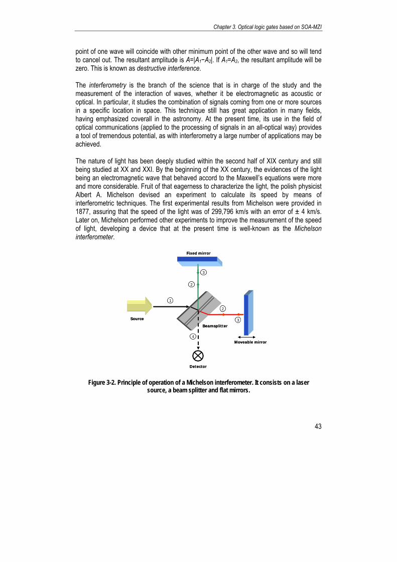
Chapter 3. Optical logic gates based on SOA-MZI
43
point of one wave will coincide with other minimum point of the other wave and so will tend to cancel out. The resultant amplitude is A=|A1−A2|. If A1=A2, the resultant amplitude will be zero. This is known as destructive interference. The interferometry is the branch of the science that is in charge of the study and the measurement of the interaction of waves, whether it be electromagnetic as acoustic or optical. In particular, it studies the combination of signals coming from one or more sources in a specific location in space. This technique still has great application in many fields, having emphasized coverall in the astronomy. At the present time, its use in the field of optical communications (applied to the processing of signals in an all-optical way) provides a tool of tremendous potential, as with interferometry a large number of applications may be achieved. The nature of light has been deeply studied within the second half of XIX century and still being studied at XX and XXI. By the beginning of the XX century, the evidences of the light being an electromagnetic wave that behaved accord to the Maxwell’s equations were more and more considerable. Fruit of that eagerness to characterize the light, the polish physicist Albert A. Michelson devised an experiment to calculate its speed by means of interferometric techniques. The first experimental results from Michelson were provided in 1877, assuring that the speed of the light was of 299,796 km/s with an error of ± 4 km/s. Later on, Michelson performed other experiments to improve the measurement of the speed of light, developing a device that at the present time is well-known as the Michelson interferometer.
Source
Fixed mirror
Moveable mirror
Detector
Beamsplitter
1
2
2
3
3
4
Source
Fixed mirror
Moveable mirror
Detector
Beamsplitter
1
2
2
3
3
4
Figure 3-2. Principle of operation of a Michelson interferometer. It consists on a laser source, a beam splitter and flat mirrors.

Capítol 3. Portes lògiques òptiques basades en SOA-MZI
44
The Michelson interferometer basically consists of a divergent optical source which, when passing through a beam splitter, is separated into two identical wave fronts, propagating in perpendicular directions, as shows Figure 3-2. These beams are reflected in individual flat mirrors, and recombined after the beam splitter. If the mirrors are placed at the same distance of the beam splitter, then, despising the differences due to the mirror’s thickness, beams interfere in phase, and no interference pattern is obtained. If one of the mirrors is scrolled, the differences in the optical paths produce an interference pattern depending on both the distance between mirrors and the wavelength of the light. Therefore, the interferometer is used to determine ranges as well as to determine wavelengths. One of the interferometers most widely used in the field of optical processing is the Mach-Zehnder interferometer, which is a variant of the Michelson’s one. This interferometer, which is showed in Figure 3-3, consists of an illumination system that generates a beam of flat waves. A beam splitter causes the light to follow two different paths. By means of mirrors the light follows a trajectory like the one shown in the Figure 3-3, and using a second beam splitter, the two contributions (which followed different optical paths) interfere. As with the Michelson Interferometer, due to the displacement of the mirrors, the differences in the optical paths will produce an interference pattern depending on both the distance between the mirrors and the wavelength of the light.
Source
Mirror
Mirror
Detector
Beamsplitter
Beamsplitter
Source
Mirror
Mirror
Detector
Beamsplitter
Beamsplitter
Figure 3-3. Principle of operation of a Mach-Zehnder interferometer. Two beamsplitters and two mirrors are used in this configuration. The light follows different optical paths
and then interferes at the output.

Chapter 3. Optical logic gates based on SOA-MZI
45
3.3. All-optical logic gates employing the SOA-MZI
The main characteristics and the principle of operation of the SOA-MZI were presented in chapter 2. The SOA-MZI (Figure 3-4) is a device with several input/output ports on each side. The ports are bidirectional in the sense that the same port can be used as an input port or an output port. This is due to the bidirectional operation of the SOAs. The interferometer is comprised of two branches in which a SOA is placed. In a basic operation the SOA acts as a nonlinear element, inducing an additional phase change on one of the signals propagating through it. This phase change is caused by another signal that can be co- or counter-propagating through the same SOA. From now on, the different configurations to achieve the logic Boolean functions and the specific use of each input/output port of the SOA-MZI will be analysed.
SOA
SOA
SOA
SOA
Figure 3-4. Mach-Zehnder interferometer with one SOA in each arm. This is known as SOA-MZI. Commercially available SOA-MZIs have 4 input and 4 output ports.
3.3.1. XOR
The XOR gate has a special interest since it is the main building block for a wide range of functions. Due to its compactness and stable structure, SOA-MZI based XOR gate seems an easy solution to achieve the integration level required for complex logic circuits [sun05]. The truth table for the XOR logic operation can be found in Appendix B. Basically, this Boolean function gives a logic “1” if the two inputs that are being compared are different (combinations A=1, B=0, and A=0, B=1). On the other hand, if the inputs are the same (combinations A=1, B=1, and A=0, B=0), the XOR output signal is a logic “0”. In the case of optical gates, the logic “1” is represented by the presence of an optical pulse, whereas the logic “0” means absence of optical power.

Capítol 3. Portes lògiques òptiques basades en SOA-MZI
46
3.3.1.1 Principle of operation
The proposed architecture for a 1-bit all-optical XOR gate is shown in Figure 3-5. It is mainly based on the SOA-MZI architecture presented in chapter 2. To perform the XOR Boolean function two optical beams carried by optical signals at the same or different wavelengths are sent through port #1 and #2 of the MZI separately. The wavelengths of the two data signals can also be the same. A train of pulses or a CW beam is coupled to port #3 as control signal. The control signal is split into two equal parts, one reaching the upper branch of the interferometer and the other reaching the lower branch. When data signals (bit sequences to be compared) are launched into the SOAs, the carrier density and, thereby, the medium refractive index is modulated. This causes a phase shift over the control signal counter-propagating through the SOAs (control signal) according to the intensity variations of the input data signals. This phase modulation experienced by the wave during propagation in the SOA is given by [ian96]:
( ) ( )[ ]002 GlnGlnLr −+=∆Φ αλ
π (3.1)
being λ the wavelength of the input data signal passing through the SOA, L the length of the active region of the SOA, α the SOA linewidth enhancement factor, r0 the refractive index in the absence of optical power, G the saturated gain and G0 the linear device gain. This equation is obtained from analytical models of wavelength converters under certain conditions such as the instantaneous response of the SOA and the adiabatic aproximation. The hypothesis that the device instantaneously responds to the modulating signal holds up to 10 Gbit/s on XPM converters [stu94]. Under the adabiatic aproximation, XPM converters have been accurately simulated by an amplifier model developed following the procedure of [mec94]. By properly setting the optical powers and the bias currents or by designing the SOA parameters, the control signal from the two SOAs can interfere either constructively or destructively at the output of the interferometer, directly performing the logic XOR operation of the two input data signals. The output intensity is proportional to
⎟⎠⎞
⎜⎝⎛ ∆−∆
∝2
212 ϕϕsinI (3.2)
where ∆φ1 and ∆φ2 are the phase changes introduced to the control signal over the upper and lower branches. The control signal entering port #3 is split into two equal parts, one reaching the upper branch of the interferometer and the other reaching the lower branch. Initially, the MZI is balanced, that is the phase shift in both branches is the same.

Chapter 3. Optical logic gates based on SOA-MZI
47
In the cases in which A=0, B=0, the control pulse enters the SOA-MZI at port #3, and then is split into two pulses, one reaching the upper SOA, and the other reaching the lower one. At this point, due to the phase shift induced at the input coupler, the phases of the two versions of the control pulse are shifted π/2. The SOAs are under the same conditions, as no data pulse has arrived to neither of them, so the phase shift is still π/2. These two pulses, after passing through the SOAs, are recombined again at the output coupler were they suffer again an additional π/2 phase shift between them. So at the output port the two pulses are with the same amplitude and with a total phase shift of π, i.e. destructive interference, and no signal is obtained.
SOA 1
SOA 2
1
43
2
data A
data B
control output
SOA 1
SOA 2
1
43
2
data A
data B
control output
Figure 3-5. XOR architecture based on a SOA-MZI. Two SOAs are symmetrically placed in each branch. XOR operation is achieved by XPM is the SOAs.
In the case A=1, B=0 (see Figure 3-6 a)), an optical pulse enters the SOA-MZI through port #1 and changes the refractive index of the upper branch SOA whereas the lower SOA remains unaffected. Thus, when the two versions of the control pulse travel through both SOAs, the phase difference between both is shifted (π is the optimum phase shift). At port #4, the signals (parts of the control signal) from the two SOAs are combined again and an optical pulse is obtained as a consequence of the constructive interference (note that the optical coupler imposes an additional π phase shift between the input signals, so the total phase shift is 2π). The same phenomenon happens if A=0 and B=1. In the case A=1, B=1 (see Figure 3-6 b)), data pulses reach both SOAs, and the phase shift induced to the control pulse in each branch is the same. As a result, at port #4 no pulse is obtained in this case due to destructive interference between the signals pulses. In a more schematic way, Figure 3-7 shows the phases of each version of the control pulse signal at different points of the SOA-MZI. As it can be seen, the couplers introduce a π/2 phase shift between the input data signals, and the SOAs may induce a differential phase

Capítol 3. Portes lògiques òptiques basades en SOA-MZI
48
shift to the signals travelling through them depending on the presence (phase shift: y) or absence (phase shift: x) of a data pulse. In some previous architectures [ian96, fje00], the control signal was a CW light which can be either in a co-propagation or in a counter-propagation scheme. However, the present architecture is configured to perform the logic XOR function using a counter-propagating optical pulse instead of a CW as the control signal. The counter-propagating scheme is preferred in order to avoid crosstalk effects, and the pulsed signal is used to reduce the full-width half-maximum (FWHM) of the output pulse, which could act as an enabling control signal to next stages.
a) b)
Figure 3-6. Detail of the signals involved in a) constructive interference and b) destructive interference. The control and data signals are depicted. The carrier
density of both SOAs and the output pulse are also showed.
3.3.1.2 Simulation study
A full characterisation of the SOA-MZI based XOR architecture was performed with computer simulations, from whose results the specifications for the laboratory demonstration were obtained. The objective of the simulation was the evaluation of the system with

Chapter 3. Optical logic gates based on SOA-MZI
49
relevant performance figures valid also for the laboratory, and with realistic specifications of commercially available devices: optical filters bandwidth, optical powers and wavelengths of laser sources, SOA-MZI parameters and bias range, etc. The schematic under study, shown in Figure 3-8, considers a single XOR gate based on a SOA-MZI, followed by an optical pass-band filter to suppress the ASE noise and to improve the OSNR. A pulsed signal in counter-propagation is used as the control signal. The input data sequences are RZ gaussian shaped pulses. The SOAs are 2-mm length biased with a 300 mA current.
SOA
SOA
0
π/2
0+x
π/2+x
0+x
π+x
SOA
SOA
0
π/2
0+x
π/2+x
0+x
π+x
a) Case A=0, B=0 (destructive interference).
SOA
SOA
0
π/2
0+y
π/2+x
0+y
π+x
π=− yx
SOA
SOA
0
π/2
0+y
π/2+x
0+y
π+x
π=− yx
b) Case A=1, B=0 (constructive interference).
SOA
SOA
0
π/2
0+y
π/2+y
0+y
π+y
SOA
SOA
0
π/2
0+y
π/2+y
0+y
π+y
c) Case A=1, B=1 (destructive interference).
Figure 3-7. Phases of each version of the control pulse at certain points of the SOA-MZI.
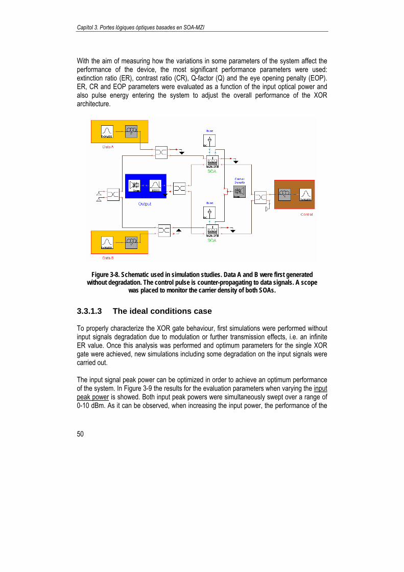
Capítol 3. Portes lògiques òptiques basades en SOA-MZI
50
With the aim of measuring how the variations in some parameters of the system affect the performance of the device, the most significant performance parameters were used: extinction ratio (ER), contrast ratio (CR), Q-factor (Q) and the eye opening penalty (EOP). ER, CR and EOP parameters were evaluated as a function of the input optical power and also pulse energy entering the system to adjust the overall performance of the XOR architecture.
Figure 3-8. Schematic used in simulation studies. Data A and B were first generated without degradation. The control pulse is counter-propagating to data signals. A scope
was placed to monitor the carrier density of both SOAs.
3.3.1.3 The ideal conditions case
To properly characterize the XOR gate behaviour, first simulations were performed without input signals degradation due to modulation or further transmission effects, i.e. an infinite ER value. Once this analysis was performed and optimum parameters for the single XOR gate were achieved, new simulations including some degradation on the input signals were carried out. The input signal peak power can be optimized in order to achieve an optimum performance of the system. In Figure 3-9 the results for the evaluation parameters when varying the input peak power is showed. Both input peak powers were simultaneously swept over a range of 0-10 dBm. As it can be observed, when increasing the input power, the performance of the

Chapter 3. Optical logic gates based on SOA-MZI
51
XOR gate improves. It can also be observed that a saturation effect exists on the ER and EOP values around 8 dBm input peak power. This effect is due to the saturation in the SOAs, at high values of the input optical power. In order to characterize the energy of the output pulses of the XOR gate, Figure 3-10 was obtained. From the figure, it can be concluded that the energy of the output pulse increases with the energy of the input pulses. Furthermore, the efficiency of the gate, considered as the output pulse energy versus the input pulse energy, becomes higher than one for input pulses of more than 150 fJ. This is a consequence from the strong saturation regime of the SOA, which is needed in order to accelerate the response of the carrier density recovery time. It is clear that a trade-off between the saturation of the SOA (and consequently the operation bit rate achievable) and the efficiency of the gate exists.
Q-fa
ctor
Eye opening penalty
Input peak power (dBm)
Q-fa
ctor
Eye opening penalty
Input peak power (dBm) Input peak power (dBm)
Extin
ctio
n ra
tio (d
B) C
ontrast ratio (dB)
Input peak power (dBm)
Extin
ctio
n ra
tio (d
B) C
ontrast ratio (dB)
Figure 3-9. Q, EOP, ER (dB) and CR (dB) values when varying the input peak power (dBm). In this study, both input peak powers were simultaneously swept over a range
of 0-10 dBm.
In a real-system application, the incoming signal arriving at the XOR gate may suffer from bit-to-bit power fluctuations arising from previous power unbalance. In this case, the performance of the subsystem can degrade because of the limited tolerance of the SOA-MZI with respect to input signal power variations. Figure 3-11 shows how the performance of the XOR correlator is affected with the variations of only one input.

Capítol 3. Portes lògiques òptiques basades en SOA-MZI
52
Figure 3-10. Output pulse energy and efficiency vs. input pulse energy. The energy of
the output pulse increases with the energy of the input pulses.
The simulation results were obtained by fixing the optical peak power of input 2 at 5 dBm and varying the input 1 optical peak power in the range of 4.5-5.5 dBm. Error-free operation is obtained over an input power dynamic range (IPDR) of 0.8 dB. The optimum point is that where the two inputs of the XOR gate have the same peak power.
Q-fa
ctor
Eye opening penalty
Input peak power (dBm)
Q-fa
ctor
Eye opening penalty
Input peak power (dBm) Input peak power (dBm)
Extin
ctio
n ra
tio (d
B) C
ontrast ratio (dB)
Input peak power (dBm)
Extin
ctio
n ra
tio (d
B) C
ontrast ratio (dB)
Input peak power (dBm)
Extin
ctio
n ra
tio (d
B) C
ontrast ratio (dB)
Figure 3-11. Evaluation of the XOR single-gate correlator performance with power variations of the incoming packet label. Variations within 1 dBm around the reference
peak power (dBm) do not drastically degrade the performance of the gate.
3.3.1.4 The non-ideal conditions case
Next, simulation results considering degradation on the input signal pulses are presented. Degradations on the input signals were introduced by adding gaussian white noise to the

Chapter 3. Optical logic gates based on SOA-MZI
53
input data signal, as showed in Figure 3-12. To consider a realistic scenario, different values for the noise power density were used in each input. In one of the input data signal the noise power spectral density was fixed to 5·10-17 W/Hz, obtaining an ER=13 dB, and for the other data signal this parameter was fixed at 2·10-17 W/Hz, obtaining an ER=17 dB. The value of ER=13 dB used in the former case was based in [ple02] experimental results. It should be noticed that the noise values considered were chosen to best fit realistic devices behaviour.
Figure 3-12. Generation procedure of degraded input signals. A gaussian white noise
block with a Noise Power Density parameter value of 5·10-17 W/Hz was used.
In this simulation study, two cases were considered and their results are presented in Figure 3-13 and Figure 3-14. In the first case (solid line) the same configuration used in previous studies was considered. In the second case (dashed line), an additional SOA placed at the output of the gate was used. The SOA works under saturation and is biased with 200 mA. The input light saturates the SOA by increase in the input power, resulting in the decrease in the ASE power from the SOA. High peak power pulses are equalised due to the slow recovery time of the SOA. Hence, the ER obtained at the output of this additional SOA is higher than that obtained at the input of the amplifier. As it can be derived from the results considering other quality signal parameters, the use of a SOA at the output improves the overall performance of the gate.
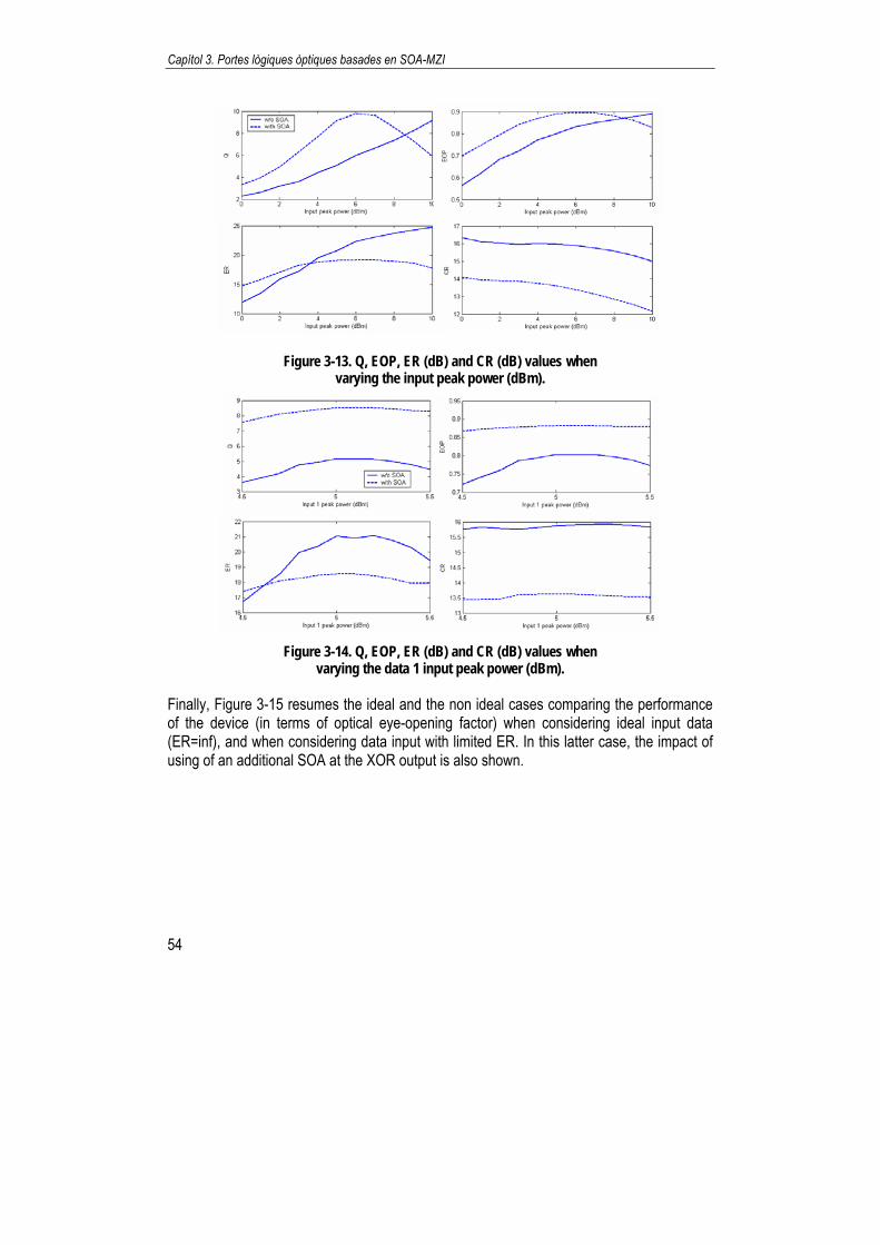
Capítol 3. Portes lògiques òptiques basades en SOA-MZI
54
Figure 3-13. Q, EOP, ER (dB) and CR (dB) values when varying the input peak power (dBm).
Figure 3-14. Q, EOP, ER (dB) and CR (dB) values when
varying the data 1 input peak power (dBm).
Finally, Figure 3-15 resumes the ideal and the non ideal cases comparing the performance of the device (in terms of optical eye-opening factor) when considering ideal input data (ER=inf), and when considering data input with limited ER. In this latter case, the impact of using of an additional SOA at the XOR output is also shown.

Chapter 3. Optical logic gates based on SOA-MZI
55
Figure 3-15. Left figure shows the optical eye-opening factor versus the input peak power. Centre figure shows the optical eye-opening factor versus some variation in the input 1 peak power. Right-side figure shows the optical eye-opening factor behaviour
with the relative mismatch between the input sequences.
3.3.1.5 Experimental validation
After the simulation characterisation of the XOR gate, experimental demonstration of the architecture was carried out in the laboratory as proof-of-concept. The logic operation addressed was a bit-by-bit XOR logic operation. Further solutions to compare more than one bit on the fly were also studied and results are presented in chapter 4. The experimental setup for the XOR gate demonstration can be split in two parts: a) data and control signal generation, and b) configuration of the SOA-MZI using these signals. The generation set-up is shown in Figure 3-17 a). Optical pulses were generated at 10 GHz repetition-rate (λ1=1556.84 nm) using a fibre-based pulsed laser (Calmar Optics) and then modulated at 10 Gbit/s using a Mach-Zehnder modulator (MZM) [rol98,sko02] (Corning) and a pattern generator (SHF). The RZ-modulated signal is then amplified using an erbium doped fibre amplifier (EDFA) filtered to minimize the ASE noise, and is split using a 3-dB

Capítol 3. Portes lògiques òptiques basades en SOA-MZI
56
coupler. One portion of the split signal is over-modulated with a train of pulses at 10 Gbit/s using a second MZM, and a polarisation beam splitter (PBS) [lia05] is used to enhance the quality of the signal. This is due to double modulation effects, which merge two different polarizations into the same signal. By using a PBS this effect is minimised and a very good signal is obtained at its output once the polarisation controllers are properly aligned, as depicted in Figure 3-166.
Time scale: 100 ps/div
Time scale: 10 ps/div
control pulse
Vertical scale: 250 µW/div Time scale: 100 ps/div
Time scale: 10 ps/div
control pulse
Vertical scale: 250 µW/div
Figure 3-16. Control pulse generated using a second MZM modulator and a PBS.
On the other hand, to generate the data signals an additional 3-dB coupler is used to split and generate data A and data B signals. As Figure 3-17 b) shows, fiber patchcords and ODLs were used to properly match the sequences and to synchronize the pulses into the SOA-MZI active region. An optical variable attenuator was placed to adjust the power of the signals. The same optical components plus a PC were used for the control signal. An optical bandpass filter centered at the signal wavelength (λC=1556.84 nm=λ1) was used to filter out ASE noise and any residual signals from data A and B (due to undesired reflections). Both SOAs were biased with 100 mA current, and the FWHM of the pulses at the input of the SOA-MZI was 10 ps7. The sequences used to test the functionality and the XOR logic operation are shown in Figure 3-18. Input peak power for the data pulses was around 1 mW and for the control pulse slightly less than 1 mW. Output pulses are near Gaussian shaped with 2 mW of peak power and a FWHM of 12 ps. The achieved ER of the output signal is higher than 13 dB. 6 The arrow on the left side of the figure gives the zero-level. 7 The FWHM values were measured with a 65 GHz optical sampling scope.
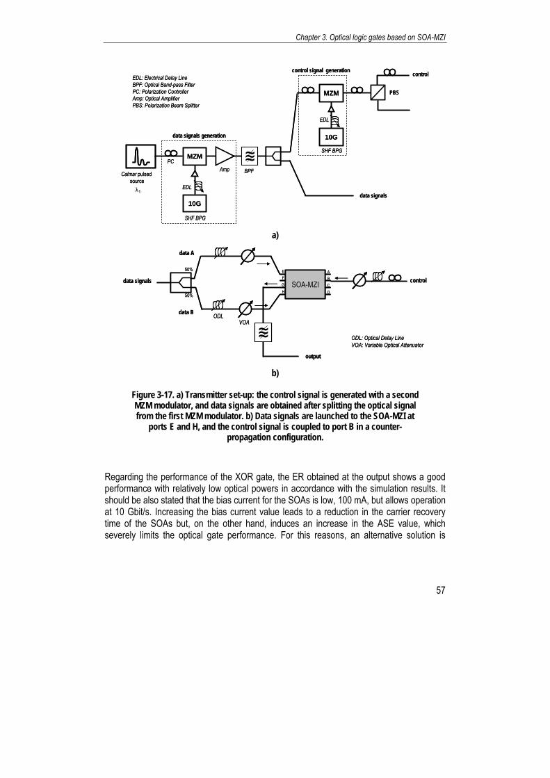
Chapter 3. Optical logic gates based on SOA-MZI
57
MZM
10G
data signals generation
Calmar pulsed source
EDL
SHF BPG
Amp
λ1
MZM
10G
control signal generation
SHF BPG
EDL
PBS
~~~
data signals
control
BPF
EDL: Electrical Delay LineBPF: Optical Band-pass FilterPC: Polarization ControllerAmp: Optical AmplifierPBS: Polarization Beam Splitter
PCMZM
10G
data signals generation
Calmar pulsed source
EDL
SHF BPG
Amp
λ1
MZM
10G
control signal generation
SHF BPG
EDL
PBS
~~~~~~
data signals
control
BPF
EDL: Electrical Delay LineBPF: Optical Band-pass FilterPC: Polarization ControllerAmp: Optical AmplifierPBS: Polarization Beam Splitter
PC
a)
SOA-MZI50%
50%
data A
E
H
GF
A
DCB
~~~
control
data B
output
data signals
ODLVOA
ODL: Optical Delay LineVOA: Variable Optical Attenuator
SOA-MZISOA-MZI50%
50%
data A
E
H
GF
A
DCB
~~~~~~
control
data B
output
data signals
ODLVOA
ODL: Optical Delay LineVOA: Variable Optical Attenuator
b)
Figure 3-17. a) Transmitter set-up: the control signal is generated with a second MZM modulator, and data signals are obtained after splitting the optical signal from the first MZM modulator. b) Data signals are launched to the SOA-MZI at
ports E and H, and the control signal is coupled to port B in a counter-propagation configuration.
Regarding the performance of the XOR gate, the ER obtained at the output shows a good performance with relatively low optical powers in accordance with the simulation results. It should be also stated that the bias current for the SOAs is low, 100 mA, but allows operation at 10 Gbit/s. Increasing the bias current value leads to a reduction in the carrier recovery time of the SOAs but, on the other hand, induces an increase in the ASE value, which severely limits the optical gate performance. For this reasons, an alternative solution is

Capítol 3. Portes lògiques òptiques basades en SOA-MZI
58
required when operating at higher bit-rates, as a differential scheme for the input signals [che02].
data A
data B
output
Time scale: 1 ns/divVertical scale: 450 µW/div
data A
data B
output
Time scale: 1 ns/divVertical scale: 450 µW/div
Figure 3-18. Experimental results at 10 Gbit/s of the XOR operation between data A and data B.
Input power fluctuations were not critical, in agreement with the simulation results. Also synchronisation accuracy is not a major issue, showing a window of 25 ps around the optimal value with good performance of the gate.
3.3.2. AND
Boolean AND operation becomes also a good choice in optical signal processing. This logic functionality, which truth table is in Appendix B, gives a logic “1” only when the two input signals under comparison are a logic “1”. In other case, the output is a logic “0”. Hybrid architectures to implement the AND logic function have been reported [awa01] in which a design based in nonlinear transmission of electro-absorption modulation with counter-propagation data streams was demonstrated. All-optical approaches have also been proposed based in: FWM in SOA [nes94], FWM in a microring resonator [mik06], XGM in SOA [sha05], XPM in SOA [sot02], polarisation switching [lee05], and cascaded single-port coupled SOAs [zha04].

Chapter 3. Optical logic gates based on SOA-MZI
59
Nevertheless, exploiting the versatility of the SOA-MZI and its previously commented advantages, the design based on MZI with SOAs is preferred.
3.3.2.1 Principle of operation
The principle of operation for the AND gate is basically the same than that for the XOR logic function. In this case, the data sequences to be compared are driven to the SOA-MZI as shown in Figure 3-19. Data signals enter the device at ports #1 and #3, while in port #2 a zero level signal must be ensured. There is no need of an additional control signal as the data signals entering the common port enables or disables the device. Following a similar principle than that of the XOR gate, an optical pulse will be obtained at the output only in the case that both data signals are “1”. In this case (A=1, B=1), the pulse of data B enables the operation. In an alternative way, the AND operation can be seen as performing the XOR comparison between data A and a zero level signal. When B=0, the gate does not produce any signal at the output as it has no signal at port #3. In the last case in which B=1 and A=0 the comparison is enabled, but as the signal at port #1 and the signal at port #2 are zero, no power is obtained at the output of the device.
SOA 1
SOA 2
1
43
2
data A
data B output
SOA 1
SOA 2
1
43
2
data A
data B output
Figure 3-19. Configuration of the SOA-MZI to implement AND logic operation.
3.3.2.2 Experimental validation
The simulation results were also validated with experimental results carried out in the laboratory. The experimental set-up is the same described in the XOR logic operation. The only change is the port at which the data signals are launched. In this case, the signals involved in the comparison are launched to the SOA-MZI as shown in Figure 3-20 b).

Capítol 3. Portes lògiques òptiques basades en SOA-MZI
60
MZM
10G
Calmar pulsed source
EDL
SHF BPG
Amp
λ1
data B
data A
PBS
MZM
10G
Calmar pulsed source
EDL
SHF BPG
Amp
λ1
data B
data A
PBS
a)
SOA-MZI
data A
E
GF
A
D
CB~~~
data Boutput H
SOA-MZI
data A
E
GF
A
D
CB~~~~~~
data Boutput H
b)
Figure 3-20. a) Generation of data A and data B signals. b) Configuration of the SOA-MZI to perform the AND logic operation.
Data A and data B were generated as showed in Figure 3-20 a) and launched in a counter-propagation scheme to the SOA-MZI. Wavelengths λA and λB were the same (1556.84 nm), and no degradation due to this was observed in the experiments due to the counter-propagation approach. If a co-propagation scheme is preferred, λA and λB must be different a separated wide enough to avoid undesired crosstalk and nonlinear effects (FWM). The separation in wavelength would be limited by the bandwidth of the filters. No pump signal was required in order to obtain better performance results at 10 Gbit/s bit rate. SOAs were biased with 100 mA of injection current. The filters used in all the experiments have a -3 dB bandwidth of 1.1 nm and a -30 dB bandwidth of 3.3 nm. The power budget of the input signals is that showed in Table 3-1. The mean ER value obtained is higher than 12 dB, which shows a good performance in order to use this output signal for further signal processing.

Chapter 3. Optical logic gates based on SOA-MZI
61
data A
data B
output
Time scale: 500 ps/divVertical scale: 1 mW/div
data A
data B
output
Time scale: 500 ps/divVertical scale: 1 mW/div
Figure 3-21. Experimental results at 10 Gbit/s of the AND operation between data A and data B. Arrows mark those cases which result in an optical pulse at the output.
Table 3-1. Peak power values for data signals involved in the AND logic operation
Signal Peak power Units
Data A 0.888 mW
Data B 1.19 mW
Output 1.67 mW
3.3.3. OR
Another logic function that may be optically implemented using the SOA-MZI based architecture is the OR. This Boolean operation, which truth table can be found in Appendix

Capítol 3. Portes lògiques òptiques basades en SOA-MZI
62
B, gives a logic “1” each time one (at least) of the input data bits is “1”. So the output of this operation only will become a “0” in the case A=0 and B=0. Although the OR operation has not been reported as much as the XOR, several implementations have been presented in the literature. One of the first approaches was [fje00a]. This scheme is based also in the use of a SOA-MZI, but it uses an additional signal to perform wavelength conversion at the same time. More recently, [kim06] proposes another versatile scheme based in the same principle.
3.3.3.1 Principle of operation
Two different architectures based on SOA-MZI can be used depending on whether it is desirable perform wavelength conversion or it is not. The simplest case is that in which no wavelength conversion is used. In this case, the principle of operation, which is depicted in Figure 3-22, is quite intuitive. The two data signals are coupled at the same port, in this case port #1. After passing through one of the two SOAs (in this case, the upper one), the amplified signal is coupled out at port #4, carrying the OR operation between the two inputs. In this case, the two inputs must be at the same wavelength and the output signal is at the same wavelength than the input signals.
SOA 1
SOA 2
1
43
2
data A
data B
output
SOA 1
SOA 2
1
43
2
data A
data B
output
Figure 3-22. Principle of operation of the OR logic gate using a SOA-MZI without wavelength conversion.
The other option is showed in Figure 3-23. In this case, the OR operation is performed over a control signal, which can be at the same or at a different wavelength than the data. The control signal is a train of optical gaussian pulses synchronised with the data pulses. This approach is more versatile since it performs, besides the logic operation, wavelength

Chapter 3. Optical logic gates based on SOA-MZI
63
conversion. In addition, in this case the input data signals could travel at different wavelengths. The principle of operation is somehow different to the first approach, and more similar to the XOR and AND gates. Here, when no pulses are coupled in into port #1, the control pulses travel through both SOAs which are symmetrically placed and biased, and arrive to the output coupler with a π phase difference due to the effect of the 3-dB couplers. That means there is a destructive interference at the output, and no signal can be found at this point. On the other hand, the presence of a data signal pulse induces a change in the carrier density of a SOA. As a result, the control pulses see different refraction indexes in each SOA. This causes an optical pulse signal at the output since destructive interference is avoided.
SOA 1
SOA 2
1
4
3
2
data A
data B
output
control5
SOA 1
SOA 2
1
4
3
2
data A
data B
output
control5
Figure 3-23. Principle of operation of the OR logic gate using a SOA-MZI and an additional control signal to perform wavelength conversion.
3.3.3.2 Experimental validation
The OR logic gate architecture validated in the laboratory is depicted in Figure 3-22. The first approach was selected as simpler than the second one, and served as proof-of-concept of the scheme. The same parameters employed in the experimental validation of the AND gate, i.e., data signal wavelength of 1556.84 nm, SOA bias current of 100 mA, and peak power of around 1 mW for both optical signals, were considered. No control signal was used, and no pump was required to work at 10 Gbit/s. The set-up for the experimental validation is showed in Figure 3-24 a) and b), and the results obtained are depicted in Figure 3-25.

Capítol 3. Portes lògiques òptiques basades en SOA-MZI
64
MZM
10G
Calmar pulsed source
EDL
SHF BPG
Amp
λ1
data A
data B
MZM
10G
Calmar pulsed source
EDL
SHF BPG
Amp
λ1
data A
data B
a)
SOA-MZI
E
GF
A
DCB ~~~ output
H
data A
data B
SOA-MZI
E
GF
A
DCB ~~~~~~ output
H
data A
data B
data Adata A
data B
b)
Figure 3-24. a) Generation of data A and data B. b) Configuration of the SOA-MZI to perform the OR logic operation.
As it can be seen, the OR Boolean operation between data A and data B is performed. In the cases in which there is at least one optical pulse at one of the inputs, an optical pulse is obtained at the output. As it can be observed from the results, there is a power fluctuation due to the optical pulse level in the case in which A=1 and B=1. This is due to the fact that this configuration is based on the coherent addition of the two optical input signals, leading to a different power level in the case A=1, B=1 with respect to the cases A=1, B=0 and A=0, B=1. In order to equalise in power the output pulses, an additional stage was added at the output of the gate. An extra SOA working under saturation regime was used employing a pump CW optical signal with -2 dBm of power at 1560 nm. The result of this operation is showed in Figure 3-26. Either using an SOA or not, the ER is always higher than 12 dB.

Chapter 3. Optical logic gates based on SOA-MZI
65
data A
data B
output
Time scale: 200 ps/divVertical scale: 2 mW/div
data A
data B
output
Time scale: 200 ps/divVertical scale: 2 mW/div
Figure 3-25. Experimental results at 10 Gbit/s of the OR operation between data A and data B.
output after SOA
output before SOA
Time scale: 200 ps/divVertical scale: 1 mW/div
Time scale: 200 ps/divVertical scale: 2 mW/div
output after SOA
output before SOA
Time scale: 200 ps/divVertical scale: 1 mW/div
Time scale: 200 ps/divVertical scale: 2 mW/div
Figure 3-26. Improvement on the OR logic gate results when using an SOA after the SOA-MZI.

Capítol 3. Portes lògiques òptiques basades en SOA-MZI
66
3.3.4. NOT
The last Boolean functionality described here is the NOT logic function. This operation of one input port and one output port inverts the input signal, so whenever there is a logic “1” at the input, a logic “0” is obtained at the output, and vice versa. A few approaches have been proposed in the literature to implement this logic functionality. Among of all them, it is interesting to bring up the approaches implemented in [hou04] and [ber06]. In [hou04] a simulation study of the NOT operation is performed by means of a SOA-assisted SAGNAC interferometer. The other approach [ber06] uses a versatile configuration based on a single SOA. The NOT logic gate here presented is based in the SOA-MZI configuration.
3.3.4.1 Principle of operation
The principle of operation of the NOT logic functionality based in SOA-MZI is depicted in Figure 3-27. There are two signals involved in this process: the original input data, and a train of optical pulses. The input data is the one to be inverted. The train of optical pulses is used to: a) generate the control signal, and b) generate an auxiliary data sequence. The input data sequence enters the SOA-MZI in port #1. The auxiliary signal, which consists in a train of pulses, is coupled into port #3 of the SOA-MZI, meanwhile the control signal is launched into port #4. The output is obtained at port #3.
SOA 1
SOA 2
1
43
2
data A
control
controloutput
SOA 1
SOA 2
1
43
2
data A
control
controloutput
Figure 3-27. Principle of operation of the NOT logic gate using a SOA-MZI.
The principle of operation is next described. The control signal enables the operation of the gate. These pulses are split and travel through the upper and lower SOAs, following symmetric paths. The lower SOA conditions will be affected by the optical pulses that are entering into port #2 (there is always an optical pulse at this port). If no pulse is present at

Chapter 3. Optical logic gates based on SOA-MZI
67
port #1, i.e. A=0, the control pulse counter-propagating through both SOAs will experience different conditions, and the initial π phase shift that the two versions of the control pulse would have at port #3 is no longer held, and non destructive interference is obtained. This means that a logic “1” will appear at the output. On the other hand, if A=1 the SOA conditions are the same so no differential phase shift is induced between the two version of the control pulse, and these will interfere destructively (due to the π phase shift induced by the 3-dB couplers at the input and output ports), resulting in no optical signal at the output (logic “0”). As a result, an inverted version of the original input data sequence is obtained at the output.
Calmar pulsed source MZM
10G
EDL
SHF BPG
Ampλ1
control
data A
PBS
Amp
~~~
~~~Calmar pulsed source MZM
10G
EDL
SHF BPG
MZM
10G
EDL
SHF BPG
AmpAmpλ1
control
data A
PBS
AmpAmp
~~~~~~
~~~~~~
a)
SOA-MZI
data A
E
GF
A
D
CB~~~
controloutput
H
control
SOA-MZI
data A
E
GF
A
D
CB~~~~~~
controloutput
H
control
b)
Figure 3-28. a) Data A and control signals generation. b) Configuration of the SOA-MZI to perform the NOT logic operation.
3.3.4.2 Experimental validation
The experimental setup used to demonstrate the logic NOT gate is shown in Figure 3-28 a) and b). The data signal A is an optical signal (RZ pulses) modulated at 10 Gbit/s with a

Capítol 3. Portes lògiques òptiques basades en SOA-MZI
68
pseudo-random bit sequence (PRBS) sequence at λA=1556.84 nm. The control signal is a train of optical gaussian pulses with a FWHM of 10 ps. The peak power of the data signal and of the signal entering at port #2 is of 2 mW and that of the control signal is of 1.5 mW. The ODLs were tuned to synchronise the data sequences at the output of the SOA-MZI. SOAs were biased with 100 mA of injection current. The attenuators were fixed to obtain the same power level for data A and the auxiliary signal, and to set the power of the control signal to obtain best performance. Figure 3-29 show the experimental results obtained when performing the NOT operation to data A. As it can be seen, the operation is successfully achieved, but as it happened with the OR gate, there is power fluctuation due to the slow recovery time of the SOAs. The ER obtained at the output signal was higher than 10 dB, and the peak power of the output pulses was between 0.8 and 1.5 mW.
NOT data A
data A
Time scale: 200 ps/divVertical scale: 1 mW/div
NOT data A
data A
Time scale: 200 ps/divVertical scale: 1 mW/div
Figure 3-29. NOT logic operation applied to data A. Data is successfully inverted, but some power fluctuation is observed in the output signal.
To minimise the power fluctuation of the output pulses an additional SOA was placed at the output of the SOA-MZI. This SOA was placed under saturation conditions, biased at 185 mA, and pumped with a CW signal of -2 dBm at 1560 nm. The results obtained after the SOA and a bandpass filter are showed in Figure 3-30. The power fluctuation is significantly reduced, and the pulses are now equalised. The peak power of the pulses is now 2 mW. The ER is improved up to 12.5 dB.

Chapter 3. Optical logic gates based on SOA-MZI
69
Time scale: 200 ps/div
output after SOA
output before SOA
Vertical scale: 1 mW/div Time scale: 200 ps/div
output after SOA
output before SOA
Vertical scale: 1 mW/div
Figure 3-30. Improvement on the NOT logic gate results when using an SOA after the SOA-MZI.
3.4. Summary and conclusions All-optical logic gates are key elements in the implementation of functionalities such as: multiplexing, signal regeneration, packet synchronisation, clock recovery, etc. In particular, SOA-based architectures are very attractive to implement these logic gates since they can exhibit a strong change of the refractive index together with high gain. Furthermore, SOAs allow for photonic integration. Concretely, SOAs under a MZI configuration show very good results, and prove to be a very versatile scheme to implement with minimum changes the most important logic functions. In this chapter, the implementation of several logic functions using a SOA-MZI as the main block has been studied. XOR, AND, OR and NOT logic operations using an all-optical approach were proposed and demonstrated in the laboratory. Their principle of operation and several simulation results to characterise the systems were described. Experimental results validate the proposed architectures, showing high versatility and good performance in accordance with the simulation results. These configurations show a very good stability on power level fluctuations of the input signals, data as well as control signals, and also on the synchronisation between pulses. The Boolean functionalities have been successfully demonstrated using low energy levels and without any additional pump signal. SOAs were biased with low injection current which leads to a low value on the total power consumption of the system.

Capítol 3. Portes lògiques òptiques basades en SOA-MZI
70
It has been stated that the use of an additional SOA at the output of the gates improves the performance in terms of ER of both OR and NOT optical logic gates. All the proposed gate architectures show good ER values, higher than 11 dB. The efficiency parameter is near one in all the experiments, In addition, the pulse width does not increase significantly, moving from the ~10 ps of FWHM at the input to ~12 ps at the output and maintaining the Gaussian shape.
3-dB coupler
SOA-MZI
Var. Attenuator
ODL
PC
3-dB coupler
SOA-MZI
Var. Attenuator
ODL
PC
Figure 3-31. Part of the experimental set-up: SOA-MZI, polarization controller (PC), optical variable attenuator, 3-dB coupler and an ODL over an optical table.
It should be noticed that all the architectures presented are all-optical solutions to implement logic gates. Therefore, the size of the experimental set-up using pigtailed components is quite large, as can be seen in Figure 3-31. However, photonic Integration seems to be a very promising solution to make this kind of architectures more compact and scalable. In fact, a layout for an integrated implementation has been designed under the framework of the FP6 Network of Excellence ePIXnet8. The photonic integration design will be addressed in detail in chapter 5. Nevertheless, results previously presented demonstrate the feasibility of the proposed configurations to implement all-optical logic functionalities.
8 http://claudia.intec.ugent.be/epixnet/

Chapter 3. Optical logic gates based on SOA-MZI
71
3.5. References [awa01] E.S. Awad, P. Cho and J. Goldhar, "High-speed all-optical AND gate using nonlinear
transmission of electroabsorption modulator", IEEE Photon. Technol. Lett., vol. 13, no. 5, pp. 472-474, 2001.
[ber06] G. Berrettini, A. Simi, A. Malacarne, A. Bogoni and L. Potí, "Ultrafast integrable and reconfigurable XNOR, AND, NOR, and NOT photonic logic gate", IEEE Photon. Technol. Lett., vol. 18, no. 8, pp. 917-919, 2006.
[che02] H. Chen, G. Zhu, Q. Wang, J. Jaques, J. Leuthold, A.B. Piccirilli, and N.K. Dutta, “All-optical logic XOR using differential scheme and Mach-Zehnder interferometer”, Electron. Lett., vol. 38, no. 21, pp. 1271-1273, 2002.
[fje00] T. Fjelde, A. Kloch, D. Wolfson, B. Dagens, A. Coquelin, I. Guillemot, F.Gaborit, F. Poingt, and M. Renaud, "Demonstration of 20 Gbit/s all-optical logic XOR in integrated SOA-based interferometric wavelength converter", Electron. Lett., vol. 36, no. 22, pp. 1863-1864, 2000.
[fje00a] T. Fjelde, A. Kloch, D. Wolfson, B. Dagens, A. Coquelin, I. Guillemot, F.Gaborit, F. Poingt, B. Dagens, and M. Renaud, "10 Gb/s all-optical logic OR in monolithically integrated interferometric wavelength converter", Electron. Lett., vol. 36, no. 9, pp. 813-815, 2000.
[hou04] T. Houbavlis, K.E. Zoiros, G. Kanellos and C. Tsekrekos, "Performance analysis of ultrafast all-optical boolean XOR gate using semiconductor optical amplifier-based Mach-Zehnder interferometer", Opt. Commun., vol. 232, no. 1, pp. 179-199, 2004.
[ian96] E. Iannone, R. Sabella, L. de Stefano and F. Valeri, "All-optical wavelength conversion in optical multicarrier networks", IEICE Trans. Commun., vol. 44, no. 6, pp. 716-724, 1996.
[kim06] J.-Y. Kim, J.-M. Kang, T.-Y. Kim and S.-K. Han, "10 Gbit/s all-optical composite logic gates with XOR, NOR, OR and NAND functions using SOA-MZI structures", Electron. Lett., vol. 42, no. 5, pp. 303-304, 2006.
[lee05] J.H. Lee, T. Nagashima, T. Hasegawa, S. Ohara, N. Sugimoto and K. Kikuchi, "40 Gb/s XOR and AND gates using polarisation switching within 1 m-long bismuth oxide-based nonlinear fibre", Electron. Lett., vol. 41, no. 19, 2005.
[lia05] T.K. Liang and H.K. Tsang, “Integrated polarization beam splitter in high index contrast silicon-on-insulator waveguides”, IEEE Photon. Technol. Lett., vol. 17, no. 2, pp. 393-395, 2005.

Capítol 3. Portes lògiques òptiques basades en SOA-MZI
72
[mec94] A. Mecozzi, “Analythical theory of four-wave mixing in semiconductor amplifiers”, Opt. Lett., vol. 19, pp. 892-894, 1994.
[mik06] S. Mikroulis, H. Simos, E. Roditi, A. Chipouras and D. Syvridis, "40-Gb/s NRZ and RZ operation of an all-optical AND logic gate based on a passive InGaAsP/InP microring resonator", IEEE/OSA J. Lightwave Technol., vol. 24, no. 3, pp. 1159-1164, 2006.
[nes94] D. Nesset, M.C. Tatham, L.D. Westbrook and D. Cotter, "Degenerate wavelength operation of an ultrafast all-optical AND gate using four wave mixing in a semiconductor laser amplifier", Electron. Lett., vol. 30, no. 23, pp. 1938-1940, 1994.
[ple02] N. Pleros, C. Bintjas, K. Yiannopoulos, G. Theophilopoulos, M. Kalyvas, K. Vyrsokinos, H. Avramopoulos, and G. Guekos, " All-optical address and data separation for 10 Gb/s packets”, in Proc. European Conference on Optical Communications, Copenhagen (Denmark), paper P4.10, 2002
[rol98] C. Rolland, “InGaAsP-based mach-zehdner modulators for high-speed transmission systems”, in Proc. Optical Fiber Communication, San Jose (California, USA), paper ThH1, 1998
[sha05] A. Sharaiha, H.W. Li, F. Marchese and J. Le Bihan, “Three inputs all-optical logic gate AND-NOR based on cross-gain modulation in a semiconductor optical amplifier”, in Proc. Conference on Lasers and Electro-optics Europe, Munich (Germany), vol. 1, pp. 503, 2005.
[sko02] E.J. Skogen, M.L. Masanovic, S.P. DenBaars and L.A. Coldren, “Monolithic integration of mach-zehnder modulators with sampled grating distributed bragg reflector lasers”, in Proc. Technical Digest Integr. Photon. Res. (IPR ’02), pages IFC3–1–IFC3–3. Vancouver (Canada), 2002.
[sot02] H. Soto, C.A. Diaz, J. Topomondzo, D. Erasme, L. Schares and G. Guekos, "All-optical AND gate implementation using cross-polarization modulation in a semiconductor optical amplifier", IEEE Photon. Technol. Lett., vol. 14, no. 4, pp. 498-500, 2002.
[stu94] K.E. Stubkjaer, “Optical wavelength converters”, in Proc. European Conference on Optical Communications, Florence (Italy), pp. 635-642, 1994.
[sun05] H. Sun, Q. Wang, H. Dong and N.K. Dutta, “XOR performance of a quantum dot semiconductor optical amplifier based Mach-Zehnder interferometer”, Opt. Express, vol. 13, no. 6, pp. 1892-1899, 2005.
[zha04] X. Zhang, Y. Wang, J. Sun, D. Liu, and D. Huang, "All-optical AND gate at 10 Gbit/s based on cascaded single-port-coupled SOAs", Opt. Express, vol. 12, no. 3, pp. 361-366, 2004.
73
Chapter 4
Optical correlator (I): Configuration based on
cascaded SOA-MZIs
4.1. Introduction In previous chapters the importance of logic gates in the field of optical signal processing was stated. A main significant application of logic gates is in future optical packet networks, which will benefit from all-optical signal processing techniques capable of recognizing optical packet headers or optical labels by comparing them with a reference address [hau02]. Typical optical label-swapping networks are based on the use of low bit rate optical labels which transport the routing information within each optical packet. The main reason of using low bit rate optical labels is the ability to electronically process them in each network node, maintaining the high bit rate packet payload in the optical domain, forwarding it without optoelectronic conversions. Among the different optical approaches to implement optical labels, the subcarrier-multiplexed (SCM) label transmission and the serial intensity–modulated (IM) label9 [gui00] are the most important techniques. In the SCM scheme [blu00, lin00], the label bits are encoded on a subcarrier, modulated in the same wavelength channel well above the baseband spectrum of the payload data. However, this approach requires the use of expensive high-frequency electronic components, making the serial IM label approach more interesting. In the IM scheme, labels are encoded as intensity-modulated signals time-preceding the data payload. 9 Also called TDM label.

Capítol 4. Correlador òptic (I): configuració basada en SOA-MZIs en cascada
74
As the packet payload bit rates increase, the optical packet label/header bit rate should increase accordingly in order to obtain good network efficiency. In this specific case, the use of all-optical label/header processing techniques over high-speed electronics may become advantageous. Therefore, optical packet networks will benefit from all-optical signal processing techniques capable of recognizing IM optical packet headers (or labels) by comparing them with a reference address [hau02]. Several IM optical label/header processing approaches have been reported in the literature [tol98, cha02, hil01, gle94]. However, most of these techniques require further optical and electronic post-processing to obtain a clear signal identifying the bit-pattern matching [tol98, cha02] or are limited to recognize specific bit-patterns [hil01, gle94]. Optical labels comparison for header processing using the logic XOR functionality has attracted interest during the last years mainly due to its easy implementation in practice [fje01, bin99, hou99, web03]. In this chapter, an all-optical packet header processor or optical correlator architecture based on optical logic XOR gates is presented. The proposed system is comprised of cascaded SOA-MZIs in the XOR configuration presented in the previous chapter. The number of SOA-MZI structures in the architecture depends on the number of bits in the header. An output optical pulse is obtained only when an address matching occurs, so the device acts as an all-optical correlator with a direct application in all-optical packet routers. Furthermore, the proposed architecture can also match arbitrary bit patterns without modifications in the system or additional signal processing. This is not the case of previously published XOR gates schemes, which can only perform the bit-by-bit comparison between two sequences, without on-the-fly identifying whether they match or not. The main application for this circuit is found in address recognition schemes within photonic routers. For example, the output pulse from the optical correlator can be used later to switch the output wavelength from an optical flip-flop, so that a tuneable wavelength converter and an AWG can route the packets to the appropriate output port, as it will be shown in chapter 6 . The simulation results presented in section 2 show that the architecture is suitable for all-optical address/label recognition at 10 Gbit/s, and the operating bit rate may also be extended to 40 Gbit/s The proposed scheme is not speed limited, except from the bandwidth limitation of current SOA technology, although several ways of overcoming this limitation have been already published [dup00,ple02,sun06]. One simple and very attractive method is the differential scheme proposed in [che02], in which the speed of operation is not limited by the carrier recovery time of the SOA. Experimental results in section 3 demonstrate the feasibility of this scheme to operate as a two-bit all-optical correlator with 10 Gbit/s optical labels. Section 4 gathers the conclusions derived from the work presented in previous sections.

Chapter 4. Optical correlator (I): Configuration based on cascaded SOA-MZIs
75
4.2. Simulation study
4.2.1. Architecture and principle of operation
The all-optical packet header processor or optical correlator architecture is shown in Figure 4-1. It is based on a cascade of SOA-MZIs. Each SOA-MZIs stage is configured to operate as a logic XOR gate as in [fje00], but using a counter-propagating scheme to avoid optical filtering between the different stages. The two input data streams are coupled into ports #1 and #2 of the MZI, while a CW light is coupled into port #4. The output signal at port #3 of the first SOA-MZI is the result of a logic XOR operation of both data streams. This output signal, after proper optical attenuation and delay, is launched into the port #4 of the second SOA-MZI synchronised with the second bit of the data patterns. The main difference between the first stage with the second and further stages is that the input signal at port #4 is not a CW signal, but a pulsed one, which acts as an enabling signal as in [mar02].
SOA
SOA
SOA
SOA
......
data input A(packet header/label)
data input B(reference inverted address)
CW input output
1st stage N-th stage
1
2
34
SOA
SOA
2nd stage
1
2
34
1
2
34
SOA
SOA
SOA
SOA
......
data input A(packet header/label)
data input B(reference inverted address)
CW input output
1st stage N-th stage
1
2
34
SOA
SOA
2nd stage
1
2
34
1
2
34
Figure 4-1. Proposed architecture for the all-optical packet header processor or optical correlator. It is based on the cascade of several SOA-MZIs operating as XOR logic
gates.
By cascading the different SOA-MZI structures the following logic function is obtained:
ij
ij
i CSS )1(1
)( −−= (4.1)
where )( j
iS is the i-th bit of the signal at the output of the j-th stage and iC is given by
iii BAC ⊕= (4.2) where Ai and Bi are the i-th bits of the input data signals to the optical header processor.
)0(iS = 1 represents the CW input signal to stage 1. By considering that the bit-length of the
data inputs and the number of stages is equal to N, the output of the whole device would be:

Capítol 4. Correlador òptic (I): configuració basada en SOA-MZIs en cascada
76
( ) ( )
⎩⎨⎧
=
≠=<=
. if,1. if,0
;,0BABA
SNiS NN
Ni (4.3)
Therefore, the architecture can be employed as an all-optical correlator for bit-pattern matching applications by introducing the one’s complement of one of both data signals (or addresses) to be compared.
time (ns)
data input A
data input B
1st stage output
2nd stage output
3rd stage output
4th stage output
word
time (ns)1 2 3 4 5 6 time (ns)
data input A
data input B
1st stage output
2nd stage output
3rd stage output
4th stage output
word
time (ns)1 2 3 4 5 6
Figure 4-2. Simulation results of bit-pattern matching (header/address recognition).

Chapter 4. Optical correlator (I): Configuration based on cascaded SOA-MZIs
77
4.2.2. Simulation results
A transmission-line laser model technique has been applied to model the SOAs [low87]. The SOAs in the MZIs are characterised by the parameters values showed in Table 4-1. The simulation results are shown in Figure 4-2. Two 10 Gbit/s data inputs (30-ps FWHM RZ gaussian pulses at 1553.6 nm) comprised of several bit patterns containing 4-bit words were applied to the correlator: A = [1000, 0011, 1110, 0100, 1011] and B = [0011, 1101, 1001, 1011, 0010]. Only the fourth word in data input B is exactly the one’s complement of the fourth word in data input A. Therefore, only an address matching pulse is expected for this word at the correlator output. The output signals from each SOA-MZI stage along the correlator are also shown in Figure 4-2. It can be seen that only an optical pulse is obtained at the output of the device (4th stage output) for the fourth data word which validates its header/address recognition functionality. The ER of the output signal is higher than 15 dB.
2 3 4 5 6 7 86
8
10
12
14
16
18
20
22
24
Ext
inct
ion
Rat
io (d
B)
Number of header/label bitsNumber of header/label bits2 3 4 5 6 7 8
6
8
10
12
14
16
18
20
22
24
Ext
inct
ion
Rat
io (d
B)
Number of header/label bitsNumber of header/label bits
Figure 4-3. Performance results against number of SOA-MZI stages. The extinction ratio is reduced by increasing the number of bits mainly due to the ASE noise
introduced by the SOAs.
The performance of the proposed architecture is dependent on the number of stages. These results are shown in Figure 4-3, where the ER of the output pulse is depicted as a function of the number of bits of the header/label. As can be seen in Figure 4-3, the ER is reduced

Capítol 4. Correlador òptic (I): configuració basada en SOA-MZIs en cascada
78
when increasing the number of bits mainly due to the accumulated ASE noise introduced by the SOAs. A maximum number of bits can be recognised depending on the ASE noise level and the required system performance. Experimental demonstrations [yux01] showed that up to 11 cascaded SOA may be used with good performance. However, the approach is still valid for all-optical label processing considering the usual number of optical nodes (different labels) in a core network [dem02].
Table 4-1. SOA parameters used in simulations
Parameter Value
SOA bias current 250 mA
SOA length 0.5 mm
SOA linewidth enhancement factor 8.0
SOA carrier lifetime 50 ps
Spontaneous emission factor 1.5
Confinement factor 0.3
4.3. Experimental validation In this section, the functionality all-optical address recognition proposed architecture is experimentally demonstrated [mar04a]. The functionality is demonstrated for 2-bit addresses, as a proof of concept of the correlator principle of operation. As an optical pulse is obtained at the output only when address matching occurs, the device operates as an all-optical correlator with application in photonic packet routers. Furthermore, the proposed architecture can identify arbitrary bit patterns without requiring further modifications in the structure or additional signal processing.
4.3.1. Set-up for two-bit correlator
The experimental set-up to validate the proposed architecture is shown in Figure 4-4. It is mainly based on a cascade of SOA-MZIs. In each SOA-MZI, data signals (bit sequences to be compared) are launched into the SOAs, so the carrier density and, thereby, the refractive index are modulated. This causes a phase shift over the signal counter-propagating through the SOAs (control signal) according to the intensity variations of the input data signals. This phase modulation experienced by the wave during propagation in the SOA is given by equation 3.1.

Chapter 4. Optical correlator (I): Configuration based on cascaded SOA-MZIs
79
By properly setting the optical powers and the SOA bias currents, the control signal from the two arms of the SOA-MZI interferes either constructively or destructively at the output of the interferometer, directly performing the logic XOR operation of the two input data signals. In the architecture, each one of these SOA-MZIs, provided by CIP10, is configured to perform the logic XOR function as in [mar04] but using a counter-propagating optical pulse instead of a CW as the control signal. The counter-propagating scheme is preferred in order to avoid crosstalk effects, and the pulsed signal is used to reduce the FWHM of the output pulse, which acts as the enabling control signal to the next stage. 10 GHz repetition-rate optical pulses with a FWHM of about 2 ps are generated at 1553 nm using a fibre-based pulsed laser, whereupon a MZM encodes the 10 Gbit/s data signals from a bit pattern generator. Different data patterns (data A and data B) are obtained by using a 50:50 optical coupler and fibre patch-cords and ODLs at the output of the label data generation module. On the other hand, the input control signal is obtained by modulating a CW optical laser with 1 GHz repetition-rate pulses of 25 ps FWHM.
~~~
MZM
data A
data B
10G
MZM
1G
label data generation
control signalgeneration
2-bit all-optical correlator ~~~
control
XOR1
XOR2
SOA
SOA
SOA
SOA
SOA-MZI2
SOA-MZI1
CW
pulsed laser
PC
PC
ODL
Att.
filter
filter
isolator
Att.
ODLs
#1
#2
#1’
#2’#3’
#3
#4’
#4
~~~~~~
MZM
data A
data B
10G
MZM
1G
label data generation
control signalgeneration
2-bit all-optical correlator ~~~~~~
control
XOR1
XOR2
SOA
SOA
SOA
SOA
SOA
SOA
SOA
SOA
SOA-MZI2
SOA-MZI1
CW
pulsed laser
PC
PC
ODL
Att.
filter
filter
isolator
Att.
ODLs
#1
#2
#1’
#2’#3’
#3
#4’
#4
Figure 4-4. Experimental set-up for the 2-bit XOR correlator.
Both RZ-modulated input data streams (data A and data B) at 10 Gbit/s with a FWHM of 9.6 ps are coupled into the upper (port #1) and lower (port #2) branches of the first SOA-MZI with 2.5 mW peak power, whereas the pulsed control signal at 1550.8 nm and with about 1 mW peak power is coupled into the common SOA-MZI port (port #3) using a counter- 10 CIP stands for The Center for Integrated Photonics.

Capítol 4. Correlador òptic (I): configuració basada en SOA-MZIs en cascada
80
propagation configuration. Both arms of the SOA-MZIs were biased with a 300 mA DC current. The length of the SOAs is 2 mm. Due to the counter-propagation operation, an isolator must also be placed between both SOA-MZI stages to avoid saturating the first stage with the second stage signals. Two tuneable filters with a -3 dB optical bandwidth of 1 nm were also used to minimize the effects of cascading the ASE noise from the SOAs. Only when a control optical pulse is injected in port #3 of the MZI, the 1-bit logic XOR operation is performed. Therefore, when several bit sequences are to be compared, the control signal consists from a train of pulses synchronized with the first bit of the data signals. The output signal from the common (port #4) of the first SOA-MZI is the result of the logic XOR operation between the first bits of each data streams. This output signal, after proper optical attenuation and delay, is launched into the common port (port #3) of the second SOA-MZI in a counter propagation configuration and synchronized with the second bit of both data patterns. This pulse acts as an enabling signal for the second logic XOR gate as in [ian96]. Hence, only if a pulse is obtained at the output of the first stage, i.e. the first bits of the data sequences compared are not the same (cases [A1=1, B1=0] and [A1=0, B1=1]), the second bits comparison (A2 and B2) is enabled at the second stage. By cascading the different SOA-MZI structures the logic function in equation 4.3 is obtained [fje00]. Therefore, the device can be employed as an all-optical correlator for bit-pattern matching applications by introducing the one’s complement of one of both data signals (or addresses) to be compared. Synchronization of the control and the incoming data signals is a critical issue that should be performed at each SOA-MZI stage to ensure a correct operation of the gates. Such synchronization must be on a bit-by-bit basis, as well as on a packet-by-packet basis [bli95]. All-optical synchronization can be achieved using ODLs to align the bit streams, as shown in Figure 4-4.
4.3.2. Experimental results
Different data patterns were used to evaluate the proposed architecture. The experimental results for the all-optical correlator are shown in Figure 4-5 for 4 different data pattern combinations: 1) A=[0 0], B=[0 1], 2) A=[1 1], B=[0 1], 3) A=[1 1], B=[0 0], and 4) A=[1 0], B=[0 1]. As it can be seen in Figure 4-5, the output from the first SOA-MZI (XOR1) is the logic XOR of the first data bits (Figure 4-5 c), whereas the output from the second SOA-MZI (XOR2) is the logic function given by equation 4.4 (Figure 4-5 d). In the first case illustrated in Figure 4-5, a data sequence [0 0] is compared with a data sequence [0 1]. The result of the first bits comparison is no pulse at the output of the first stage ([A1=0, B1=0]), so the comparison at the second stage in disabled. In the second case,

Chapter 4. Optical correlator (I): Configuration based on cascaded SOA-MZIs
81
a data sequence [1 1] is compared with a data sequence [0 1]. In this case, a pulse is obtained as a result of the first stage comparison ([A1=1, B1=0]), and this pulse enables the comparison at the second stage. In the second stage no pulse is obtained at the output as a result of the second bits comparison ([A2=1, B2=1]). In this latter case, the “0” logic pulse obtained at the output is consequence of comparing two “1” pulses at the input. This is the most critical comparison as a very good destructive interference is needed to cancel the signal at the output. A residual signal is observed in this latter case as a result of slight power level mismatch of both input pulses.
a)
b)
c)
d)
a)
b)
c)
d)
Figure 4-5. Experimental results: (a) data A, (b) data B, (c) XOR1, and (d) XOR2. (X axis time scale: 50 ps/div.)
An ER of 13 dB and peak power values higher than 5 mW were obtained at the output, which are very appropriated to control further subsystems within a photonic packet-switching node. A FWHM of 12.8 ps was obtained for the output pulses from the correlator.

Capítol 4. Correlador òptic (I): configuració basada en SOA-MZIs en cascada
82
Some performance results for the 2-bit optical correlator are also shown in Figure 4-6. The Q-factor and the ER were measured as a function of the peak power of the input data pulses. As it can be seen in Figure 4-6, error-free operation is obtained for a 4 dBm input peak power, whereas ER values around 13 dB are obtained for about 2 dBm input peak powers. The experimental results (dots) for the Q-factor and the ER were fitted using a linear approximation and a quadratic function (lines), respectively, showing an excellent agreement. The behaviour of the ER curve shows an optimum performance point caused by the saturation of the SOA-MZIs for high power levels.
-4 -2 0 2 4 6 82
3
4
5
6
7
8
9
10
11
12
Input peak power (dBm)
Q-fa
ctor
-4 -2 0 2 4 6 86
7
8
9
10
11
12
13
14
Input peak power (dBm)
Extin
ctio
n R
atio
(dB)
-4 -2 0 2 4 6 82
3
4
5
6
7
8
9
10
11
12
Input peak power (dBm)
Q-fa
ctor
-4 -2 0 2 4 6 86
7
8
9
10
11
12
13
14
Input peak power (dBm)
Extin
ctio
n R
atio
(dB)
Figure 4-6. Q-factor and ER for different input peak powers. The experimental results (dots) for the Q-factor and the ER were fitted using a linear approximation and a
quadratic function (lines), respectively, showing an excellent agreement.
However, the performance of the architecture is dependent on the number of stages. The simulation results showed that the ER is reduced by increasing the number of bits, mainly due to the ASE noise introduced by the SOAs. A maximum number of bits can be recognized depending on the ASE noise level and the desired performance. Nevertheless, it may be foreseen that the approach is a valid option for all-optical label processing considering the number of nodes in the proposed AOLS networks.

Chapter 4. Optical correlator (I): Configuration based on cascaded SOA-MZIs
83
4.4. Summary and conclusions In this chapter, a novel scheme for all-optical packet header recognition has been proposed. The novel architecture provides a solution for all-optical recognition of arbitrary data patterns. The scheme is not only a bit-by-bit based XOR gate, but it can identify arbitrary bit patterns without requiring any further modification in the scheme or additional signal processing techniques. This way, the proposed scheme readily implements an all-optical header processor, which directly provides the result of a two bit patterns comparison. The architecture is based on cascaded SOA-MZIs, which provides potentiality to build a fully photonic-integrated circuit. A suitable application for label recognition in all-optical routers is envisaged. The simulation results at 10 Gbit/s show the feasibility of the proposed scheme, although the technique may be also extended to higher bit rates. Nevertheless, the performance is degraded when increasing the number of SOA-MZI stages. Hence, a maximum number of bits can be processed depending on the ASE noise levels. Simulations show that 6 SOA-MZI can be used in a cascade configuration with an ER higher than 10 dB. Experimental demonstrations [yux01] showed that up to 11 cascaded SOA may be used with good performance. A 2-bit all-optical correlator based on cascaded SOA-MZIs was demonstrated at 10 Gbit/s. Error-free operation with 13 dB extinction-ratio performance was achieved after the second stage by carefully adjusting the input data powers. In principle, the proposed scheme is not speed limited, except from the bandwidth limitation of current SOA technology, although several ways of overcoming this limitation have been already published [dup00, ple02, sun06]. One simple and very attractive method is the differential scheme proposed in [che02], in which the speed of operation is not limited by the carrier recovery time of the SOA. The scheme is intended to identify arbitrary bit patterns without requiring a modification in the scheme or additional signal processing techniques as it happens in other architectures [fje01, tak04]. The main application for this circuit is found in address recognition schemes within photonic routers. For example, the output pulse from the optical correlator can be used later to switch the output wavelength from an optical flip-flop, so that a tuneable wavelength converter and an AWG can route the packets to the appropriate output port, as it will be shown in chapter 6 .

Capítol 4. Correlador òptic (I): configuració basada en SOA-MZIs en cascada
84
4.5. References [agr97] G.P. Agrawal, "Fiber Optic Communication Systems - 2nd Edition", Ed. Wiley, N. Y.,
1997.
[bin00] C. Bintjas, M. Kalyvas, G. Theophilopoulos, T. Stathopoulos, L. Occhi, L. Schares, G. Guekos, S. Hansmann, and R. Dall’Ara, "20 Gb/s all-optical XOR with UNI gate", IEEE Photon. Technol. Lett., vol. 12, no. 7, pp. 834-836, 2000.
[bli95] P. Blixt and J.E. Bowers, "An optical technique for bit and packet synchronization", IEEE Photon. Technol. Lett., vol.7, no.1, pp.123-125, 1995.
[blu99] D.J. Blumenthal, A. Carena, L. Rau, V. Curri, and S. Humphries, “All-optical label swapping with wavelength conversion for WDM-IP networks with subcarrier multiplexed addressing”, IEEE Photon. Technol. Lett., vol. 11, no. 11, pp. 1497-1499, 1999.
[cha02] K. Chan, F. Tong, C.K. Chan, L.K. Chen, and W. Hung, “An all-optical packet header recognition scheme for self-routing packet networks”, in Proc. Optical Fiber Communication, Anaheim (California, USA), paper WO4, pp. 284-285, 2002.
[che02] Y.K. Chen, C.J. Hu, C.C. Lee, K.M. Feng, M.K. Lu, Y.K. Tu, and S.L. Tzeng, “All-optical logic XOR using differential scheme and Mach-Zehnder interferometer”, Electron. Lett., vol. 38, no. 21, pp. 1271-1273, 2002.
[dem02] S. De Maesschalck, D. Colle, I. Lievens, M. Pickavet, P. Demeester, “Pan-European Optical Transport Networks: an Availability-based Comparison”, Photonic Network Communications, vol. 5, no. 3, pp. 203-225, 2002.
[dup00] M.A. Dupertuis, J.L. Pleumeekers, T.P. Hessler, P.E. Selbmann, B. Deveaud, B. Dagens, and J.Y. Emery, “Extremely fast high-gain and low-current SOA by optical speed-up at transparency”, IEEE Photon. Technol. Lett., vol. 12, no. 11, pp. 1453-1455, 2000.
[fje00] T. Fjelde, A. Kloch, D. Wolfson, B. Dagens, A. Coquelin, I. Guillemot, F. Gaborit, F. Poingt, and M. Renaud, “Demonstration of 20 Gbit/s all-optical logic XOR in integrated SOA-based interferometric wavelength converter”, Electron. Lett., vol. 36, no. 22, pp. 1863-1864, 2000.
[fje01] T. Fjelde, A. Kloch, D. Wolfson, B. Dagens, A. Coquelin, I. Guillemot, F. Gaborit, F. Poingt, and M. Renaud, "Novel scheme for simple label-swapping employing XOR logic in an integrated interferometric wavelength converter", IEEE Photon. Technol. Lett., vol. 13, no. 7, pp. 750-751, 2001.
Chapter 4. Optical correlator (I): Configuration based on cascaded SOA-MZIs
85
[gle94] I. Glesk, J.P. Solokoff, and P.R. Prucnal, “All-optical address recognition and self-routing in a 250 Gbit/s packet-switched network”, Electron. Lett., vol. 30, no. 16, pp. 1322-1323, 1994.
[gui00] C. Guillemot, M. Henry, F. Clerot, A. Le Corre, J. Kervaree, A. Dupas, P. Gravey, “KEOPS optical packet switch demonstrator architecture and testbed performance”, in Proc. Optical Fiber Communication Conference, Baltimore (Maryland, USA), vol. 3, pp. 204-206, 2000.
[hau02] M.C. Hauer, J. McGeehan, J. Touch, P. Kamath, J. Bannister, E.R. Lyons, C.H. Lin, A.A. Au, H.P. Lee, D.S. Starodubov, and A.E. Willner, “Dynamically reconfigurable all-optical correlators to support ultra-fast Internet routing”, in Proc. of Optical Fiber Communication, Anaheim (California, USA), paper WM7, pp. 268-270, 2002.
[hil01] M.T. Hill, A. Srivatsa, N. Calabretta, Y. Liu, H. de Waardt, G.D. Khoe, and H.J.S. Dorren, “1x2 optical packet switch using all-optical header processing”, Electron. Lett., vol. 37, no. 12, pp. 774-775, 2001.
[hou99] T. Houbavlis, K. Zoiros, A. Hatziefremidis, H. Avramopoulos, L. Occhi, G. Guekos, S. Hansmann, H. Burkhard, and R. Dall’Ara, "10 Gbit/s al-optical boolean XOR with SOA fibre Sagnac gate", Electron. Lett., vol. 35, no. 19, pp. 1650-1652, 1999.
[ian96] E. Iannone, R. Sabella, L. de Stefano, and F. Valeri, "All-optical wavelength conversion in optical multicarrier networks", IEEE Trans. on Comm., vol. 44, no. 6, pp. 716-724, 1996
[lin00] Y.M. Lin, W.I. Way, and G.K. Chang, “A novel optical label swapping technique using erasable optical single-sideband subcarrier label”, IEEE Photon. Technol. Lett., vol. 12, no. 8, pp. 1088-1090, 2000
[low87] A.J. Lowery, “A new dynamic semiconductor laser model based on the transmission line modeling method”, IEE Proc. J. Optoelectron., vol. 134, pp. 281-289, 1987.
[mar02] J.M. Martinez, F. Ramos, J. Marti, J. Herrera, and R. Llorente, “All-optical N-bit XOR gate with feedback for optical packet header processing”, in Proc. 28th European Conference on Optical Communications, Copenhagen (Denmark), vol. 3, pp. 1-2, paper P4-8, 2002.
[mar04] J.M. Martinez, F. Ramos, and J. Marti, “All-optical packet header processor based on cascaded SOA-MZIs”, Electron. Lett., vol. 40, no. 14, pp. 894-895, 2004.
[mar04a] J.M. Martínez, R. Clavero, F. Ramos, J. Martí, "All-Optical Header Recognition Scheme for All-Optical Packet Routers in Optical Label-Swapping Networks", on Proc. 30th European Conference on Optical Communications, Stockholm (Sweden), vol. 3, paper We4.P.129, pp. 726-727, 2004.

Capítol 4. Correlador òptic (I): configuració basada en SOA-MZIs en cascada
86
[ple02] J.L. Pleumeekers, M. Kauer, K. Dreyer, C. Burrus, A.G. Dentai, S. Shunk, J. Leuthold, and C.H. Joyner, “Acceleration of gain recovery in semiconductor optical amplifiers by optical injection near transparency wavelength”, IEEE Photon. Technol. Lett., vol. 14, no. 1, pp. 12-14, 2002.
[sun06] H. Sun, Q. Wang, H. Dong, Z. Chen, N.K. Dutta, J. Jaques, and A.B. Piccirilli, “All-optical logic XOR gate at 80 Gbi/s using SOA-MZI-DI”, IEEE J. Quantum Electron., vol. 42, no. 8, 2006.
[tak04] R. Takahashi, T. Nakahara, H. Takenouchi, and H. Suzuki, “40-Gbit/s label recognition and 1x4 self-routing using Self-Serial-to-Parallel conversion”, IEEE Photon. Technol. Lett., vol.16, no.2, pp. 692-694, 2004.
[tol98] P. Toliver, R.J. Runser, K.L. Deng, B.Y. Yu, and P.R. Prucnal, “Routing of 100 Gb/s words in a packet-switched optical networking demonstration (POND) node”, IEEE/OSA J. Lightwave Technol., vol. 16, no. 12, pp. 2169-2180, 1998.
[web03] R.P. Webb, R.J. Manning, G.D. Maxwell, and A.J. Poustie, “40 Gb/s all-optical XOR gate based on hybrid-integrated Mach-Zehnder interferometer”, Electron. Lett., vol. 39, no. 1, pp. 79-81, 2003.
[yux01] J. Yu and P. Jeppesen, “Improvements of cascaded semiconductor optical amplifier gates by using holding light injection”, IEEE/OSA J. Lightwave Technol., vol. 19, no. 5, 2001.

87
Chapter 5
Optical correlator (II): N-bit logic XOR gate with
feedback
5.1. Introduction As stated in previous chapters, it is a fact that there is an increasing interest in performing the key networking functionalities in the optical domain to achieve bit rate transparency. Among them, optical header processing would enable fast reading and forwarding optical packets in future all-optical packet-switched core networks. Plenty of the optical header processing functions are based on all-optical logic gates, in which the logic XOR gate shows its key importance in decision and comparison circuits. Chapter 4 presented an architecture which performs all-optical packet header processor or optical correlation. It was based on the use of cascaded SOA-MZIs, and the experimental results showed good performance for 2-bits labels comparison. However, as the pattern length in the label increases, the number of cascaded SOA-MZIs required to perform the optical correlation also increases, and so do the size and the complexity. In order to obtain an optical header processor architecture fully scalable, or at least fully competitive, a step forward on the evolution of the integration technology of optical components and devices is required. In this chapter, a novel architecture of an N-bit logic XOR gate based on a MZI with feedback is presented. The architecture consists of an integrated SOA-MZI, an optical pulsed control signal, a differential transmission scheme for the input data sequences for bit rates up to 40 Gbit/s (not required operating at 10 Gbit/s), and a feedback network. This architecture uses a single SOA-MZI device to perform the comparison of optical data

Capítol 5. Correlador òptic (II): Porta lògica XOR de N bits amb re-alimentació
88
sequences comprising several bits, which simplifies the system in terms of size and complexity. In section 2 the performance of the proposed device is first evaluated by means of simulations, and then is experimentally evaluated in the lab and the results are showed in section 3. The mask design for an integrated version of the device using the InP platform is presented in section 4. Conclusions are addressed in section 5.
5.2. Simulation study
5.2.1. Principle of operation
Optical header recognition operations with logic gates are based on the packet header comparison with a specific address ‘keyword’. The most suitable implementation using logic XOR gates performs the comparison using the packet header and the 1’s-complement of the address ‘keyword’ as inputs of the XOR gate. When two data streams are applied to the inputs of an all-optical logic XOR gate, a series of optical pulses appear at its output (e.g. an optical pulse is obtained each time that the two bits from data streams are different). This way, the address matching can be identified when the result is a train of N optical pulses at the output of the logic XOR gate, being N the number of bits of the packet header and the address ‘keyword’. The equation describing the output of a conventional XOR gate is:
iii bax ⊕= (5.1) where A = [a1 a2 ... aN] and B = [b1 b2 ... bN] are the input data and X = [x1 x2 ... xN] is the XOR output.
τdelay
C
XB
A
τdelay
C
XB
A
Figure 5-1. Schematic diagram of the N-bit logic XOR gate using a single device. A feedback loop is used as enabling signal of the gate.
Additional signal processing (e.g. using an optical correlator or logic AND gate with the output pulses) is needed to implement packet header identification schemes as the XOR gate is memoryless. To solve this drawback and avoid latter signal processing, an architecture using a feedback loop as enabling signal of the XOR gate is proposed. This way, the packet header recognition scheme can be implemented employing a single

Chapter 5. Optical correlator (II): N-bit logic XOR gate with feedback
89
functional block. This novel device, a N-bit logic XOR gate, is illustrated schematically in Figure 5-1. The equation describing the output of the N-bit logic XOR gate can be expressed as (i ≥ 1)
( ) ( ) '1', 01 =⋅⊕=⋅⊕= − xxbacbax iiiiiii (5.2) where ci is the enabling signal. As a result, the address matching can be identified by reading just the N-th bit at the output of the XOR device (e.g. xN = ‘1’ represents address matching).
5.2.2. Proposed architecture
The all-optical N-bit XOR gate with feedback architecture is shown in Figure 5-2. This architecture consists of an integrated SOA- MZI, a pulsed control optical signal, a differential transmission block and a feedback network. The SOA-MZI of Figure 5-2 performs the 1-bit XOR operation between the two data signals [fje00]. Both data signals are first combined in the differential block in a 'push-pull' arrangement [web03] or so-called differential scheme, and then coupled into ports #1 and #2 of the SOA-MZI, while a control signal is coupled into port #4. Data signals and the control signal counter-propagate inside the SOAs to avoid crosstalk. In this architecture a pulsed optical signal is used as the control signal. This control signal enables the device operation. Only when an optical pulse is present at the input #4 of the SOA-MZI the 1-bit logic XOR operation is performed. Therefore, the control signal must be a train of pulses synchronized to the first bit of the data signals to be compared. Furthermore, the output of the SOA-MZI (port #3) is also an optical pulse (if the first two bits of both sequences are different), which after optically processed is feedback to the input of the SOA-MZI (port #4) as an enabling signal for the comparison of the next two bits. As long as the bits in the inputs are different, optical pulses are obtained at the device output. In the case the compared bits are the same, no pulse at the output of the SOA-MZI is obtained and therefore the following pulses will not be compared as the gate is disabled. In the feedback loop of Figure 5-2 the signal is filtered to reduce ASE noise, attenuated to achieve the proper optical power and delayed to match the incoming data pulses, as previously reported [mar02]. The main difference between the previous approach presented in chapter 4 and the architecture presented here is the differential block applied to the data streams to be compared. This technique reduces the constraint imposed by the slow recovery times of the SOA, enabling the operation with 40 Gbit/s data sequences.

Capítol 5. Correlador òptic (II): Porta lògica XOR de N bits amb re-alimentació
90
Data streams are combined in the following way before going through the SOA-MZI: in port #1 of the SOA-MZI, data stream A is combined with a delayed and attenuated version of data stream B (Figure 5-3d), while in port #2, data stream B is combined with a delayed and attenuated version of data stream A (Figure 5-3e). The control signal is coupled into port #4. In the SOA-MZI, the data signals from the differential block are launched into the SOAs where the carrier density and, thereby, the refractive index are modulated as previously described by equation 3.1.
Figure 5-2. Proposed architecture of the N-bit XOR gate with feedback.
By properly setting the optical powers, the SOA parameters and the bias currents, the control signal from the two SOAs interferes either constructively or destructively at the output of the MZI (port #3) depending on the phase changes to perform the logic XOR operation of the two input data signals. As can be seen in Figure 5-3f, when data A and data B are different, e.g. data A is ‘1’ and data B is ‘0’, the phase change is induced first on the upper branch and a switching window opens. Later, when the phase change on the lower branch is also induced, the differential phase is cancelled and the switching window closes [che02]. As a result, a pulse appears at the output of the SOA-MZI (Figure 5-3g). On the other hand, when data A and data B are the same, the phase change in both branches is the same and no light is generated at the output of the SOA-MZI (Figure 5-3g).

Chapter 5. Optical correlator (II): N-bit logic XOR gate with feedback
91
(a)
(b)
(c)
(d)
(e)
(f)
(g)
Figure 5-3. XOR operation. (a) control signal at port #4, (b) data A, (c) data B, (d) combined signal at port #1, (e) combined signal at port #2, (f) SOA carrier densities, (g)
output signal at port #3.
In those architectures without the differential scheme, the slow SOA recovery time is critical, limiting the operation to 10 Gbit/s. The use of SOAs also introduces a limitation due to the pulse broadening. The use of long SOAs with slow recovery times may lead to a considerable pulse broadening, which may result in inducing pulse interference, further limiting the operating bit rate of the gate. It should be noticed that the proposed architecture must be implemented as a photonic integrated circuit (PIC) due to the SOA-MZI structure. Moreover, a speed constraint due to the feedback functionality in this structure exists. The maximum overall loop delay allowed by the gate is given by ∆τ = 1/R, where R is the bit rate (100 ps @ 10 Gbit/s, 25 ps @ 40 Gbit/s). The use of new promising technologies such as two-dimensional photonic crystal (2D-PC) slabs for manufacturing ultra-small PICs are a suitable choice to implement the proposed architecture solving the speed constraint of the feedback loop. Recently, a 2D-PC-based symmetric Mach-Zehnder type ultrafast all-optical switch with buried quantum dots as optical nonlinear materials has been proposed [sug02]. In addition, it should be stated that the overall loop gain must be set close to unity, as higher values result in the SOA saturation and lead to instabilities, but lower values vanish feedback pulses.

Capítol 5. Correlador òptic (II): Porta lògica XOR de N bits amb re-alimentació
92
5.2.3. Simulation results
5.2.3.1 Validation of device operation
Intensive realistic simulations of the N-bit logic XOR gate architecture were carried out (using again the Virtual Photonics Inc. Software) to evaluate the proposed architecture. Two gaussian pulsed sources at 1555.21 nm with a peak power of –1.25 dBm are used for generating the binary sequences to be compared, while a third one at 1570.68 nm (+6 dBm peak power) produces the pulsed control signal. As can be seen in Figure 5-4, wavelengths were chosen for placing the data signals inside an amplified region of the SOA curve whereas the control signal is inside a less amplified region. The pulses from the optical sources have a FWHM of 4.5 ps. Both SOAs in the MZI are characterized by a length of 200 µm. During the simulations, a CW pump signal of 15 mW at 1567.74 nm has been also applied to the MZI in order to accelerate the SOAs carrier density response [gir98], although it is not shown in Figure 5-2. The parameters of the feedback loop are an optical attenuation of 3.4 dB, a delay of 14.5 ps and a filter bandwidth of 1.5 nm.
1490 1500 1510 1520 1530 1540 1550 1560 1570 1580 1590-12
-10
-8
-6
-4
-2
0
Wavelength (nm)
Nor
mal
ized
SO
A g
ain
(dB
)
noise floor
datasignals
controlsignal
Figure 5-4. Simulated SOA gain spectral response and placement of data and control signals.
In order to verify the principle of operation, a comparison between two 4-bit-length words was carried out with the proposed N-bit XOR gate and the simulation results at 40 Gbit/s are shown in Figure 5-5. The control signal optical pulses (Figure 5-5a) will enable the comparison of the first two bits of each word. The input data sequence A is: [1101 1001

Chapter 5. Optical correlator (II): N-bit logic XOR gate with feedback
93
0010], whereas the input data sequence B is: [0010 0100 0111], as depicted in Figure 5-5b and Figure 5-5c, respectively. The 4-bit logic XOR operation between both data sequences may be obtained by extracting the 4th bit of the output XOR data signal employing an EAM gate (Figure 5-2) as shown in Figure 5-5d. It is found that the XOR output data pulses have a FWHM of ~5.3 ps. For the sake of comparison, the output of a conventional XOR gate is also shown in Figure 5-5e, where it can be seen that the optical gate is memoryless as the bits from the two data sequences are individually compared.
a)
b)
c)
d)
e)
gating
Figure 5-5. Optical signals: (a) Control signal. (b) Input data A. (c) Input data B. (d) Output N-bit XOR data. (e) Conventional XOR gate.
5.2.3.2 Performance evaluation
In order to asses the performance of the proposed approach, the BER of the optical XOR signal at the output of the device for two 40 Gbit/s input PRBS signals against the received optical power was evaluated for different number of bits in the sequences. These results will determine the impact of the successive bit comparisons. In fact, it is expected that the control optical pulses will be progressively degraded after passing several times through the feedback loop in the device due to the pulse broadening introduced by the SOAs. The results are shown in Figure 5-6, where it may be deduced the power penalty as a function of the number of bits to be compared. From Figure 5-6, it can be seen that as the number of bits of the word increases from 1 to 8 a power penalty of about 1.32 dB (@ BER = 1·10-12) is introduced. The ER is greater than 16 dB for all the cases.
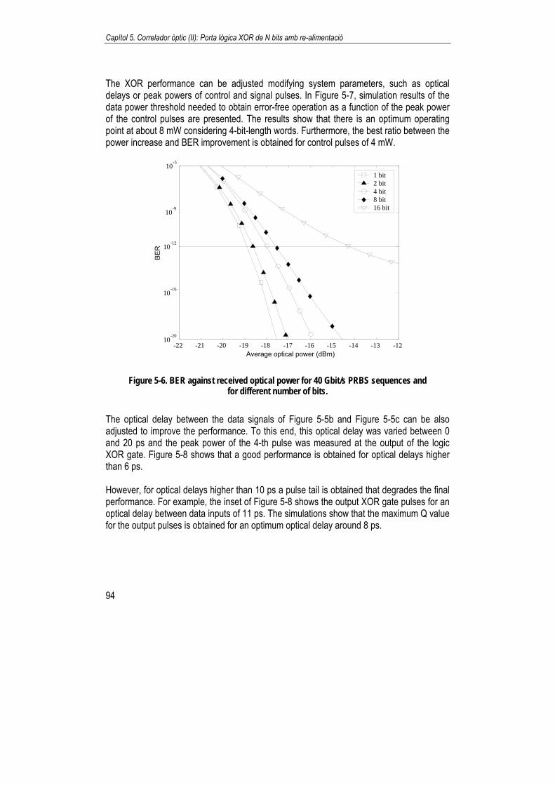
Capítol 5. Correlador òptic (II): Porta lògica XOR de N bits amb re-alimentació
94
The XOR performance can be adjusted modifying system parameters, such as optical delays or peak powers of control and signal pulses. In Figure 5-7, simulation results of the data power threshold needed to obtain error-free operation as a function of the peak power of the control pulses are presented. The results show that there is an optimum operating point at about 8 mW considering 4-bit-length words. Furthermore, the best ratio between the power increase and BER improvement is obtained for control pulses of 4 mW.
-22 -21 -20 -19 -18 -17 -16 -15 -14 -13 -1210
-20
10-16
10-12
10-9
10-5
Average optical power (dBm)
BE
R
1 bit2 bit4 bit8 bit16 bit
Figure 5-6. BER against received optical power for 40 Gbit/s PRBS sequences and for different number of bits.
The optical delay between the data signals of Figure 5-5b and Figure 5-5c can be also adjusted to improve the performance. To this end, this optical delay was varied between 0 and 20 ps and the peak power of the 4-th pulse was measured at the output of the logic XOR gate. Figure 5-8 shows that a good performance is obtained for optical delays higher than 6 ps. However, for optical delays higher than 10 ps a pulse tail is obtained that degrades the final performance. For example, the inset of Figure 5-8 shows the output XOR gate pulses for an optical delay between data inputs of 11 ps. The simulations show that the maximum Q value for the output pulses is obtained for an optimum optical delay around 8 ps.

Chapter 5. Optical correlator (II): N-bit logic XOR gate with feedback
95
1 2 4 8 16 32-19
-18.5
-18
-17.5
-17
-16.5
-16
Control power (mW)
Ave
rage
pow
er th
resh
old
for e
rror-
free
oper
atio
n (d
Bm)
Figure 5-7. Data power threshold for error-free operation as a function of peak power of control pulses.
0 2 4 6 8 10 12 14 16 18 200.1
0.2
0.3
0.4
0.5
0.6
0.7
0.8
0.9
1
Delay between data inputs (ps)
Nor
mal
ized
pea
k po
wer
Figure 5-8. Optimization of optical delay between data inputs to the interferometer.

Capítol 5. Correlador òptic (II): Porta lògica XOR de N bits amb re-alimentació
96
0 1 2 3 4 5 6 7 8 9 100.3
0.4
0.5
0.6
0.7
0.8
0.9
1
Delay between control signal and data inputs (ps)
Nor
mal
ized
pea
k po
wer
Figure 5-9. Optimization of optical delay between data and control pulses.
In addition, simulation results showed that introducing a specific delay between the data inputs and the counter-propagating control pulses the final performance can be also enhanced. Figure 5-9 shows the peak power of the output pulses normalized to its maximum as a function of the optical delay between the data signal pulses and the control pulses. As can be seen in Figure 5-9, for optical delays around 4-6 ps, the best performance is obtained. This effect is caused because the control pulses arrive at the SOAs immediately after the data signals have passed through them and the initial transient effects are avoided. In the same way as commented above, considering the Q-factor performance an optimum delay of 6 ps is obtained. Once the main parameters of the N-bit XOR gate were properly adjusted, a sensitivity analysis over several operation conditions was performed. For example, Figure 5-10 shows the eye opening of the output XOR pulses as a function of the data signals peak power. As can be seen in Figure 5-10, the optimum operating point is for a peak power of -1.25 dBm. Anyway, the performance shows low sensitivity to variations in the peak power of both data A and B signal pulses, considering that the peak power of both data A and B signal pulses are the same. On the other hand, if their peak powers are different, the situation changes. In this case, the performance is degraded as the peak power of one data signal is lower than -1.25 dBm. These results are shown in Figure 5-11, where it can be seen that the dynamic range peak powers of data A lies between -2 to 3 dBm for a -1.25 dBm data B peak power.

Chapter 5. Optical correlator (II): N-bit logic XOR gate with feedback
97
-6 -5 -4 -3 -2 -1 0 1 2 3 40.9
0.91
0.92
0.93
0.94
0.95
0.96
0.97
0.98
0.99
1
Peak power of data pulses (dBm)
Eye
ope
ning
fact
or
Figure 5-10. Performance sensitivity to variations in optical power of data signals (the same peak power for both data signals).
-6 -5 -4 -3 -2 -1 0 1 2 3 40.6
0.65
0.7
0.75
0.8
0.85
0.9
0.95
1
Peak power of data A pulses (dBm)
Eye
open
ing
fact
or
Figure 5-11. Performance sensitivity to variations in optical power of data A signal (peak power of data B signal equal to –1.25 dBm).
Finally, the results of performance sensitivity were extender to wavelength/frequency shifts in the optical carriers of data signals as shown in Figure 5-12. In this case, the wavelength of data B pulses is fixed at 1555.21 nm whereas the wavelength of data A pulses is shifted from 1554.8 nm to 1556.2 nm. As can be seen in Figure 5-12, there is a range of positive frequency shifts up to 0.6 THz for which optimum performance is obtained. This is because a negative frequency shift in data signals provides a reduction of SOA gain but also reduces
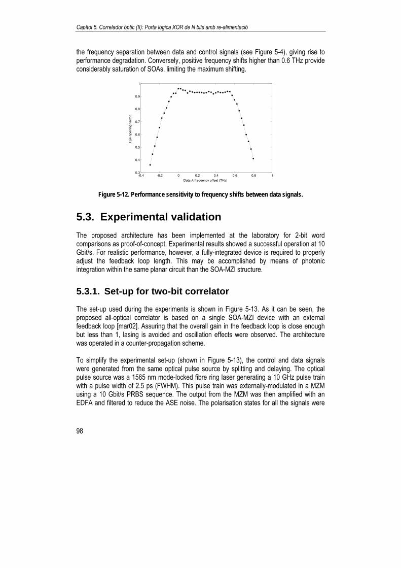
Capítol 5. Correlador òptic (II): Porta lògica XOR de N bits amb re-alimentació
98
the frequency separation between data and control signals (see Figure 5-4), giving rise to performance degradation. Conversely, positive frequency shifts higher than 0.6 THz provide considerably saturation of SOAs, limiting the maximum shifting.
-0.4 -0.2 0 0.2 0.4 0.6 0.8 10.3
0.4
0.5
0.6
0.7
0.8
0.9
1
Data A frequency offset (THz)
Eye
ope
ning
fact
or
Figure 5-12. Performance sensitivity to frequency shifts between data signals.
5.3. Experimental validation The proposed architecture has been implemented at the laboratory for 2-bit word comparisons as proof-of-concept. Experimental results showed a successful operation at 10 Gbit/s. For realistic performance, however, a fully-integrated device is required to properly adjust the feedback loop length. This may be accomplished by means of photonic integration within the same planar circuit than the SOA-MZI structure.
5.3.1. Set-up for two-bit correlator
The set-up used during the experiments is shown in Figure 5-13. As it can be seen, the proposed all-optical correlator is based on a single SOA-MZI device with an external feedback loop [mar02]. Assuring that the overall gain in the feedback loop is close enough but less than 1, lasing is avoided and oscillation effects were observed. The architecture was operated in a counter-propagation scheme. To simplify the experimental set-up (shown in Figure 5-13), the control and data signals were generated from the same optical pulse source by splitting and delaying. The optical pulse source was a 1565 nm mode-locked fibre ring laser generating a 10 GHz pulse train with a pulse width of 2.5 ps (FWHM). This pulse train was externally-modulated in a MZM using a 10 Gbit/s PRBS sequence. The output from the MZM was then amplified with an EDFA and filtered to reduce the ASE noise. The polarisation states for all the signals were

Chapter 5. Optical correlator (II): N-bit logic XOR gate with feedback
99
controlled at the SOA-MZI inputs for an optimum performance. Each of the SOA-MZI couplers has a 3 dB splitting ratio. The SOAs are characterised by a length of 2 mm, a gain of 20 dB and a saturated gain recovery time of 25 ps. Synchronisation between the data and the control pulses is a must to obtain the proper operation for the device and this was achieved with adjustable ODLs. To demonstrate the device functionality at the lab with commercially available pigtailed components, the feedback loop can be performed with external fiber patchords and using repeating words for the data sequences to be compared, so that the control signal can be synchronised with a subsequent word.
#2
#4
50:50
50:50
data BSOA
SOA
SOA-MZI
ODL
#1
#3
data A
PCPCAtt.
ODL
Att.
output
10G PRBS
MZM
1565 nm
10 GHz∼∼∼∼∼∼∼∼∼ pulsedlaser
EDFA
1565 nm
∼∼∼∼∼∼∼∼∼
PCPC
ODL
1565 nm
PCPCAtt.
PCPCAtt.
control
all-optical correlator
Figure 5-13. Experimental set-up for the N-bit optical correlator based in a SOA-MZI with external feedback loop.
5.3.2. Principle of operation
The principle of operation for the architecture is as follows. The SOA-MZI acts as an standard logic XOR gate to perform bit to bit comparisons between the two input data words at ports #1 and #2, whereas the feedback loop provides the optical memory capability to keep the result from previous bit to bit comparisons. A single pulse (control signal) introduced through port #3 enables the logic gate to start the XOR operation between both data words. If the first two bits to be compared are different (e.g. “0” and “1”, or “1” and “0”), an optical pulse is obtained at the SOA-MZI output port #4. After proper attenuation, filtering and delay through the feedback loop, the pulse is synchronised to the following two bits to be compared and driven again into the SOA-MZI input port #3 as an enabling signal. At the SOA-MZI output, optical pulses are obtained

Capítol 5. Correlador òptic (II): Porta lògica XOR de N bits amb re-alimentació
100
whenever the two bits to be compared are different. If any bit comparison result is zero (e.g. inputs are “0” and “0”, or “1” and “1”), the logic gate is disabled and no output pulses are obtained for the remaining bits. As a result, gating the last bit at the output, the following logic function can be obtained:
⎪⎩
⎪⎨⎧
=
≠=
. if,1
. if,0
BA
BAS (5.3)
where A and B are the input data signals. According to equation 5.3, the architecture can be used as an optical correlator to implement the address-matching functionality within photonic routers or add-drop multiplexers. To this end, the 1’s complement of the local address is introduced as one of the two data words. The other one is the incoming packet header or label. If the packet header or label matches the address data sequence, then an output pulse is obtained at the last bit position. After time gating, this is the output signal from the optical correlator. The principle of operation is schematically depicted in Figure 5-14. For a practical device, the feedback loop needs to be as short as possible, because the feedback loop length sets the maximum operation bit rate. This can only be achieved with a fully-integrated device. To demonstrate the device functionality at the lab, however, this can be accomplished by closing the feedback loop with external pigtails and using repeating words for the data sequences to be compared, so that the control signal can be synchronised with a subsequent word. The device operation was tested employing all the possible combinations of 2-bit words. Some of these results are shown in Figure 5-15. Each inset corresponds to the signal measured at the output of the SOA-MZI for a specific combination of two input data words. As depicted in this figure, the XOR correlator works as explained before. By checking the last bit of the output signal (marked with the arrow), an address matching can be found. In this specific case, the address matching is obtained for the comparison between data words [0 1] and [1 0], as they are exactly the 1’s complement each other. The measured ER for the output signal was around 6 dB (output peak power pulses of 1.5 mW). Although the results show a successful operation to implement address matching functions, it is expected that the performance may be optimised by using a fully-integrated device to reduce the feedback loop length.

Chapter 5. Optical correlator (II): N-bit logic XOR gate with feedback
101
...
...
...
0 01 00 01 1
1 10 1 1 10 1
...
data A(packet labels)
data B(local labels)
control
output fromcorrelator
matching
Figure 5-14. Principle of operation: data A, data B, control signal and output from the correlator. The last bit gives the results of the data signals comparison.
00-00 01-00
01-1001-11
10-10 10-00
matching
Figure 5-15. Output from the correlator for different input data words (2 bits length).

Capítol 5. Correlador òptic (II): Porta lògica XOR de N bits amb re-alimentació
102
5.4. Design of a mask layout for a PIC The XOR logic gate with feedback has been proved to be a very useful solution to deal with the problems related to scalability. Results with discrete components demonstrated the architecture’s principle of operation, and served as a proof of concept. However, a practical implementation is only possible by using an integrated version of this architecture. A two-month stay in the Technical University of Eindhoven (TU/e) in collaboration with the COBRA group was arranged to the aim of designing a mask layout of the integrated version of the device, and a subsequent fabrication. This collaboration was supported by the FP6 network of excellence ePIXnet.
5.4.1. ePIXnet
The "European Network of Excellence on Photonic Integrated Components and Circuits" is an European FP6 research project. ePIXnet11 provides a platform to its academic and industrial partners for sharing and integrating research facilities and know-how in the field of photonic integrated components and circuits. There are five Facility Access Activities (FAA) in the network. The FAAs are long-lasting research co-operations centred on a unique and expensive facility (for fabrication or characterisation issues). The work developed in this section of the Thesis was part of the activities in FAA1, which aims to disseminate, exploit and extend the know-how on the modelling, design and fabrication of monolithic photonic integration by combining the COBRA expertise in integration of optical amplifiers and passive optical devices with complementary know-how from the other partners.
5.4.2. Design of the mask layout
The work within these two-month stage aimed the definition and specification of the mask layout for an all-optical N-bit XOR logic gate with feedback. The work was mainly carried out using the simulation tool MDS for performing simulations and several C library routines to create the files needed for the mask definition. In the first period of the stage some simulations were performed aiming to obtain an optimised set of parameters which were used later in the mask design. For example, the characterisation of the optimum waveguide offset in order to efficiently convert straight section waveguides to curved ones, and also between two curved section waveguides. Figure 5-16 shows an example on a circuit layer employed for the simulation study of deep waveguides straight-curve adaptation for deep-etched waveguides. Simulations reported 11 http://claudia.intec.ugent.be/epixnet/

Chapter 5. Optical correlator (II): N-bit logic XOR gate with feedback
103
that the optimum value for the offset was dependent on the radii of the waveguides curve: the higher the radii, the higher the required offset between waveguides.
Figure 5-16. Circuit layer for the simulation study of deep waveguides sc adaptation.
After the initial period, the definitive mask design was approached. The second period comprised the complete definition of the mask layout for the N-bit XOR optical gate with feedback.
MMI coupler
MMI coupler
MMI coupler
MMI coupler
MMI coupler
Variable Attenuator
AWG-based BP filter
SOA
SOA
Data A
Data B
Control
Output
MMI coupler
MMI coupler
MMI coupler
MMI coupler
MMI coupler
Variable Attenuator
AWG-based BP filter
SOA
SOA
Data A
Data B
Control
Output
Figure 5-17. First design serving as an initial approach for the mask layout of the PIC.
The architecture considered for the all-optical XOR gate with feedback was that described in previous sections. Figure 5-17 shows a first design for the integrated version of the device. Basically, the device consists of an SOA-MZI and a feedback loop. The feedback loop is

Capítol 5. Correlador òptic (II): Porta lògica XOR de N bits amb re-alimentació
104
comprised of an optical bandpass filter at 1550 nm to reject the out-of-band ASE noise from the SOAs plus an optical attenuator. The complete feedback loop must have a length as short as possible in order to deal with bit rates in the order of Gbit/s. In fact, the device was designed to work at 10 Gbit/s, and this could only be possible with a photonic integrated device. The next task was to define how this architecture could become completely integrated. InP-based photonic integration technology [bin04] was chosen to implement the device. Integration in indium phosphide (InP) semiconductor materials allows the combination of passive (wavelength (de)multiplexing, splitting, coupling) and active (light generation, amplification, detection, modulation) functions in the same material system and by wafer scale processing alone. The fabrication process of InP PICs can be divided into two stages: first, the integration of the various active and passive waveguide layers, and second, the waveguide processing. Figure 5-18 show the passive and active layer stack.
3e17
Q1.25p-Q1.25
p-InP
Q1.55
n-InP
14050200
120
500
n.i.d.1e173e17
n.i.d.
3.5e17n-Q1.25 190 6e16
I-5I-6I-7
I-4
I-1I-3
p-Q1.25 20III-1
n-InP sub 1-4e18I-0
p-InP
Material
1000
d [nm]100
1e18
doping1.5e19max
III-3
#III-4
p-InP 300 5e17III-2
p-InGaAs
3e17
Q1.25p-Q1.25
p-InP
Q1.55
n-InP
14050200
120
500
n.i.d.1e173e17
n.i.d.
3.5e17n-Q1.25 190 6e16
I-5I-6I-7
I-4
I-1I-3
p-Q1.25 20III-1
n-InP sub 1-4e18I-0
p-InP
Material
1000
d [nm]100
1e18
doping1.5e19max
III-3
#III-4
p-InP 300 5e17III-2
p-InGaAs
1000
200360
500140
1e18
n.i.d.6e16
3.5e176e16
p-InP
InPn-Q1.25
n-InPn-Q1.25
III-3
II-2II-1
I-1I-2
20 3e17p-Q1.25III-1
Material d [nm]100
doping1.5e19max
#III-4
300 5e17p-InPIII-2
n-InP sub 1-4e18I-0
p-InGaAs1000
200360
500140
1e18
n.i.d.6e16
3.5e176e16
p-InP
InPn-Q1.25
n-InPn-Q1.25
III-3
II-2II-1
I-1I-2
20 3e17p-Q1.25III-1
Material d [nm]100
doping1.5e19max
#III-4
300 5e17p-InPIII-2
n-InP sub 1-4e18I-0
p-InGaAs
a) b)
Figure 5-18. Layers stack: a) active, b) passive.
The SOA-MZI block consists of two active regions and two MMI couplers. The SOAs are 1 mm length and 2.0 µm wide, and are connected to 3.0 µm passive waveguides using adiabatic tapers. Waveguides are split and recombined using 2x2 multi-mode interference (MMI) couplers. The MMIs are symmetric 50/50 couplers having a width wmmi=8.0 µm and a length of 268.8 µm. The phase shifter is 2.5 mm length and 2.0 µm wide. The AWG is a low-loss compact Phasar [smi88], centered at λ=1.55 um, with a channel spacing of 3.22 nm, and a free spectral range of 16 nm. The refractive index of the waveguides is 3.17.

Chapter 5. Optical correlator (II): N-bit logic XOR gate with feedback
105
The total length of the loop is approximately 8.3 mm, which should be enough in order to work at 10 Gbit/s (designed bit rate operation). In addition, some extra passive devices for testing purposes were also included in the final mask design. Figure 5-19 shows the definitive mask layout for the device.
SOA1
SOA2
MMI
AWG
Phase shifter
monitor
monitorin
in
out
SOA1
SOA2
MMI
AWG
Phase shifter
monitor
monitorin
in
out
Figure 5-19. Definitive mask layout for the InP prototype.
The yellow shadowed zones indicate deep-etched waveguides, which are used in curved sections with high radius (R=500 µm). Red shadowed areas indicate the presence of active layers, for the SOAs and for the phase shifter. The MMI couplers were terminated in a rippled shape to avoid undesired back-reflections. The use of 2x2 MMI couplers in a SOA-MZI instead of 1x2 couplers improves the optical bandwidth of such devices [han04]. The final PIC will be delivered by the end of this year, first to be characterised, and then to test the functionality.
5.5. Summary and conclusions In this chapter, a novel optimized architecture to perform all-optical logic XOR function between two words has been proposed. The architecture is based on a single SOA-MZI with an external feedback loop, comprised of a filter, an ODL and an attenuator. The proposed architecture seems extremely promising because a single SOA-MZI device performs the comparison of arbitrary-length data words. This would result in a simple and scalable solution for packet header processing in optical add-drop multiplexers and optical cross-connects in high-speed optical networks. Simulation results at 40 Gbit/s showed a very good performance up to 16-bit length words, with ER values higher than 16 dB. However, to operate at this bit rate, a differential scheme is required due to the low recovery time of the SOAs. The operational parameters of the N-bit logic XOR gate such as optical powers or optical delays between signals have been optimised. The simulation results show that the best performance is obtained for an optical delay between data inputs to the interferometer of 8 ps, an optical delay between data signals and control signal of 6 ps, and peak power of data pulses of –1.25 dBm. The sensitivity analysis carried out shows that any unbalancing between the data signal parameters may considerable degrade the final performance

Capítol 5. Correlador òptic (II): Porta lògica XOR de N bits amb re-alimentació
106
considerably. Dynamic ranges of 5 dBm in optical power variation and 0.6 THz in frequency shifts between data signals were obtained. This architecture has been also experimentally demonstrated at 10 Gbit/s employing 2-bit length sequences. No differential scheme was used since SOAs could work with 10 Gbit/s signal bit rate. Every possible combination of 2 bits length words was successfully demonstrated, showing good performance in terms of ER. However, photonic integration is required in order to achieve better performance and fully scalability. To obtain a 100-ps round-trip time in the feedback loop (10 Gbit/s operation), small radius waveguide bends are needed which can be achieved employing high-index silica waveguides (~1-mm radius) or other fabrication technologies such as a deep/shallow double etching process (~100-µm radius) [hil05]. To this aim, an initial layout for an integrated version of this architecture has been already delivered. Experimental results from the resulting integrated device are expected for the incoming year.

Chapter 5. Optical correlator (II): N-bit logic XOR gate with feedback
107
5.6. References [bin04] J.J.M. Binsma, J.H. den Besten, and R.G. Boreke, “InP-based photonic integration
technology”, in Proc. IPR 2004, San Francisco (USA), paper IFB1, 2004.
[che02] H. Chen, G. Zhu, Q. Wang, J. Jaques, J. Leuthold, A. B. Piccirrilli, and N. K. Dutta, “All-optical logic XOR using differential scheme and Mach-Zehnder interferometer”, Electron. Lett., vol. 38, no. 21, pp. 1271-1273, 2002.
[fje00] T. Fjelde, D. Wolfson, A. Kloch, B. Dagens, A. Coquelin, I. Guillemot, F. Gaborit, F. Poingt, and M. Renaud, “Demonstration of 20 Gbit/s all-optical logic XOR in integrated SOA-based interferometric wavelength converter”, Electron. Lett., vol. 36, no. 22, pp. 1863-1864, 2000.
[gir98] F. Girardin, G. Guekos, and A. Houbavlis, “Gain recovery of bulk semiconductor optical amplifiers”, IEEE Photon. Technol. Lett., vol. 10, no. 6, pp. 784-786, 1998.
[han04] R. Hanfoug, L.M. Augustin, J.J.G.M. van der Tol, R.G. Broeke, and M.K. Smit, “Optical bandwidth of Mach-Zehnder interferometer wavelength converters”, in Proc. IPR 2004, San Francisco (USA), paper JWB19, pp. 1-3, 2004.
[hil05] M.T. Hill, T. de Vries, H.J.S. Dorren, X.J.M. Leijtens, J.H.C. van Zantvoort, J.H. den Besten, E. Smalbrugge, Y.S. Oei, J.J.M. Binsma, G.D. Khoe, and M.K. Smit, “Integrated two-state AWG-based multiwavelength laser”, IEEE Photon. Technol. Lett., vol. 17, no. 5, pp. 956-958, 2005.
[mar02] J.M. Martinez, F. Ramos, J. Marti, J. Herrera, and R. Llorente, “All-optical N-bit XOR gate with feedback for optical packet header processing”, in Proc. 28th European Conference on Optical Communications, Copenhagen (Denmark), vol. 3, pp. 1-2, paper P4-8, 2002.
[sug02] Y. Sugimoto, N. Ikeda, N. Carlsson, and K. Asakawa, “Fabrication and characterization of different types of two-dimensional AlGaAs photonic crystal slabs”, J. Appl. Phys., vol. 91, no. 3, pp. 922-929, 2002.
[web03] R. P. Webb, R. J. Manning, G. D. Maxwell, and A. J. Poustie, “40 Gbit/s all-optical XOR gate based on hybrid-integrated Mach-Zehnder interferometer”, Electron. Lett., vol. 39, no. 1, pp. 79-81, 2003.
[smi88] M.K. Smit, “New focusing and dispersive planar component based on an optical phased array”, Electron. Lett., vol. 24, no. 7, pp. 385-386, 1988.


109
Chapter 6
Applications of all-optical logic gates in practical
scenarios
6.1. Introduction Future all-optical networks will require high bit rates optical data packets to be routed through all-optical nodes. In the nodes of core telecommunication networks, electro-optical conversion and ultra fast electronics are required to process optical signals. However, physical and technological limitations make extremely difficult for the electronics to operate at very high frequencies, which makes these devices extremely expensive. In fact, almost 90% of the cost of any core network lies in modules that perform electro-optical conversion. Consequently, there is a rapidly growing need and interest in developing satisfactory all-optical signal processing. Therefore, for future transparent and high-throughput packet routing, it is envisaged that the packet header/label bits must be all-optically recognized and further the packet routed/switched properly [hil01, hau02]. So far, most of the proposed architectures address the packet header processing electronically [koo02] and/or take the routing/switching decisions employing electronic control circuitry [wad02, xia98, tak04, mor03]. Furthermore, the true really all-optical schemes previously reported are limited to single-bit header reading and/or 1x2 optical packet switching [hil01, gle97, cot95], which cannot be generally considered as a realistic packet routing. In this chapter, sections 2 and 3 present a novel architecture to perform label reading and packet routing all-optically based on logic gates and flip-flops. Section 2 addresses the study of the proposed architecture by means of simulation, and section 3 gives some experimental results of a modified version of this architecture.

Capítol 6. Aplicacions de los portes lògiques completament òptiques en un escenari pragmàtic
110
In a complementary plane, electronic computers work with binary, on or off, states. An optical computer would require that a light beam may turn another on and off. This was first achieved with the photonic transistor (Rocky Mountain Research Center, 1989). This demonstration eventually created a growing interest in all-optical photonic logic technology using light interference. A first step towards this photonic logic is presented in the Spanish funded I+D+I Multilogic project. Section 4 gives an overview of this project, presenting the main objectives and the initial device design based on the use of SOA-MZIs to implement reconfigurable Boolean gates and other switching functionalities. Conclusions are commented in section 5.
6.2. All-optical packet routing scheme based on SOA-MZIs: a first approach
In this section, a novel scheme for all-optical label reading and packet routing based on logic XOR gates and flip-flops is presented. This architecture is may be a milestone in the development of all-optical packet routers in label-swapping networks [blu05]. Conversely to header/label recognition methods previously proposed [hil01, cot95], the approach described here allows the recognition of arbitrary words without any kind of ‘keyword’ coding. The basic building blocks of the proposed architecture are potentially integrated SOA-MZIs.
6.2.1. All-optical packet router architecture
The proposed architecture is shown in Figure 6-1. When a packet arrives to the optical node, its header/label is extracted and sent to an array of optical correlators (Figure 6-1) where it is compared with several reference address keywords (look-up table entries) by using all-optical logic XOR gates based on single SOA-MZI devices (Figure 6-2) [mar02, mar04, fje00]. The reference address keywords can be all-optically generated employing the approach shown in [cot95]. By using this technique, the address keywords are automatically generated after each packet arrival without the need of additional synchronization. Each XOR gate is followed by an all-optical flip-flop which emits a signal at λi when it is in "high" state, as it is shown in Figure 6-1. Previously to the comparison, an optical pulse (set signal) is applied to all optical flip-flops to set their outputs to "high" state (Figure 6-2). The principle of operation of the XOR gate used is that described in chapter 3. If both data inputs to a specific correlator (XOR gate) are identical, no output pulse is obtained and the associated flip-flop continues emitting at λi. Conversely, if any of the bits of both data inputs is different, one or several pulses are obtained at the output of the XOR gate (Figure 6-2). These pulses reset the corresponding all-optical flip-flops and no signals appear at their outputs.

Chapter 6. Applications of all-optical logic gates in practical scenarios
111
All-opticalXOR gatecorrelator
.
.
.
.
.
.
.
.
.
New label generation
and insertion
All-opticalflip-flop
λ1
All-opticalXOR gatecorrelator
All-opticalflip-flop
λN
Ref. Address#1
Ref. Address#N
WavelengthConverter
.
.
.
AWG
.
.
.
1 x NSplitter N x 1
Combiner
Label
PayloadLabel/payload
separation
(A)
(C)
(F)
(E)
#1
#N
Output ports
(D)(B)
(H)(G)
Delay line
All-opticalXOR gatecorrelator
.
.
.
.
.
.
.
.
.
.
.
.
New label generation
and insertion
All-opticalflip-flop
λ1
All-opticalXOR gatecorrelator
All-opticalflip-flop
λN
Ref. Address#1
Ref. Address#1
Ref. Address#N
Ref. Address#N
WavelengthConverter
.
.
.
AWG
.
.
.
1 x NSplitter N x 1
Combiner
Label
PayloadLabel/payload
separation
(A)
(C)
(F)
(E)
#1
#N
Output ports
(D)(B)
(H)(G)
Delay line
Figure 6-1. All-optical packet router architecture.
The structure of the all-optical flip-flop based on a single SOA-MZI device (Figure 6-2) has been proposed and evaluated for the first time [cla05]. Similar architectures make use of a minimum of two SOA-MZIs [hil01a]. A CW optical signal at λi is launched into the input port of the SOA-MZI. The input and output couplers provide both a phase shift of π/2 between both MZI branches. Therefore, in absence of other input signals no optical signal is obtained at the SOA-MZI output as a consequence of a destructive interference at the output coupler. As it is shown in Figure 6-2, this output port is interconnected through a feedback loop to the lower SOA-MZI branch with an 80/20 coupler. In the feedback loop, a 2x2 coupler with an adjustable coupling factor is also used to extract the output signal from the all-optical flip-flop and introduce the set pulses which act as enabling signals. Finally, another 80/20 coupler is used in the upper SOA-MZI branch to balance the interferometer and introduce the reset pulses. When a set pulse is injected (Figure 6-2), it reaches the lower SOA and reduces its carrier density and differential gain. The SOA-MZI is now unbalanced and the CW signal experiences different gains in both MZI branches, which results in an output power at point (D).

Capítol 6. Aplicacions de los portes lògiques completament òptiques en un escenari pragmàtic
112
CW λi
Reset signal
Set signal
Control signal
Header/Label
Ref. Address #n
New Label + Payload
Output
All-opt ical correlator based on XOR gate All-opt ical flip-flop Wavelength converter
SOA
SOA
SOA
SOA
SOA
SOA
SOA
SOA
SOA
SOA
SOA
SOA
.
.
.
N x 1Combiner
(B)
(C) (D)
(E)
(G)
(F)
Figure 6-2. Detailed diagrams of some of the simulated elements and their interconnection.
The feedback loop forwards a fraction of this output power through the couplers again to the lower SOA to hold its state when the optical power of the set pulse vanishes. Conversely, when a reset pulse is injected, it arrives to the upper SOA and reduces its carrier density and gain in a similar way, but due to the feedback loop the carrier density in the lower SOA is also changed. If the energy of this reset pulse is high enough a change in the state of the flip-flop occurs, and the MZI is balanced again. By employing this flip-flop, low switching energies (<2 pJ pulses) and fast operation (<1 ns response delays) may be achieved [cla05]. In optical label swapping networks, the packet header usually is a serial intensity-modulated optical label [blu00]. A new-label insertion circuit is also needed to swap the previously extracted incoming label by a new one, as shown in Figure 6-1. Finally, the optical flip-flop outputs are combined and applied to an SOA-MZI wavelength converter (Figure 6-1) [fje99], jointly with the optical packet to be routed (the payload and the new label inserted). The packet is then converted to λi, the optical wavelength corresponding to the output of the unique flip-flop in "high state" (i.e. the correlator branch where both the corresponding packet label and the reference address match). The wavelength conversion of the payload allows for the packet routing by using an AWG or similar techniques (Figure 6-1) [hil01]. As it can be deduced from the architecture shown in Figure 6-1, only a limited address space is available due to the scalability driven by space integration, driving current and the optical losses in the splitters/combiners needed to compare the incoming packet header/label with all the keyword addresses. However, this approach may be still valid for all-optical label processing considering the typical number of optical nodes (different labels/addresses) in a core network which can be estimated in a maximum of 256 [cae04].

Chapter 6. Applications of all-optical logic gates in practical scenarios
113
6.2.2. Simulation results of all-optical packet routing
The proposed packet routing scheme was validated by means of simulations with 10 Gbit/s packets. The label/header of each data packet was previously processed employing logic XOR gates and the packet routed according to it. Four different wavelengths used to route the data packets were generated during the simulations employing optical flip-flops. For the simulations, parameters shown in Table 6-1 were considered, and the label/payload separation and new-label generation and insertion circuits were assumed ideal. Some techniques for a practical implementation of these circuits are reported in [tsi03, ols00]. The simulation results are shown in Figure 6-3. Four 10 Gbit/s data packets (30 ps FWHM gaussian RZ pulses with 0.16 pJ energy at 1553.6 nm) with different optical labels were generated (Figure 6-3a). The optical signal-to-noise ratio (SNR) of the packets was 25 dB. The number of bits in the label was 4 whereas the payload had a 128-bit length.
Table 6-1. Simulation parameters.
Parameter Value
XOR gate + wavelength converter
SOA bias current 250 mA
SOA length 0.5 mm
SOA linewidth enhancement factor 8.0
SOA carrier lifetime 300 ps
Noise figure 8 dB
Flip-flop
SOA bias current 100 mA
SOA length 0.5 mm
SOA linewidth enhancement factor 8.0
SOA carrier lifetime 1.1 ns
Noise figure 8 dB
Energy of set pulses 1.55 pJ
Energy of reset pulses 1.5 pJ
CW input power +3 dBm
Capítol 6. Aplicacions de los portes lògiques completament òptiques en un escenari pragmàtic
114
The labels of the packets were chosen to match each one of the four reference address keywords. For each optical packet reset pulses are obtained at the output of each correlator when there is no matching between the compared data words. This happens for all the branches but one in Figure 6-1 during the time duration of each packet. For example, the second packet label matches the fourth reference address. Therefore, at the fourth correlator output there will be no reset pulses for the second packet, as it is shown in Figure 6-3b. A stable CW signal (see Table 6-2) is generated for the whole duration of the packet at the output of the only flip-flop where no reset pulses are present. Following the previous example, this can be seen in Figure 6-3c. This optical signal was used to perform wavelength conversion of the packet and further routing through the AWG. The optical packets routed to each output port are shown in Figure 6-3d-g. As it can be seen, the first packet is wavelength-converted to λ2 (Figure 6-3e), the second one to λ4 (Figure 6-3g), the third one to λ1 (Figure 6-3d) and the fourth one to λ3 (Figure 6-3f). The optical spectra of each packet are also shown in Figure 6-3d-g as insets. In the simulations, a pump signal at 1558.44 nm was also applied to both the XOR-based correlator and also the wavelength converter to accelerate the SOAs carrier density response [gir98]. For 40 Gbit/s operation, a differential phase-modulation scheme should be used at the SOA-MZIs [che02]. Two 1.6-nm optical bandpass filters were also placed between the SOA-MZIs to reduce the accumulated noise, although not shown in Figure 6-2. The performance of the wavelength conversion process depends on signal level at the flip-flops output. The optical powers at each flip-flop output are shown in Table 6-2. There are small variations due to the flip-flop parameters were the same for all of them. Each flip-flop, however, can be optimized independently to obtain the same output powers. Finally, the BER of the routed packets was estimated in the simulations. In Figure 6-4, the measured error-rates show that a penalty of 0.45 dB penalty is obtained for the worst case of routed packets. The eye diagram can be also seen in Figure 6-4 as an inset showing a clear open eye. Polarization issues were neglected during the simulations, as optimum polarisation states are assumed for the set-up. Additional power penalties would arise if the polarizations are not correctly adjusted during the experiments, especially in the case of the SOA-MZI input signals.

Chapter 6. Applications of all-optical logic gates in practical scenarios
115
reset
set
label payload
input data packets
4th flip-flop inputs
4th flip-flop output
output port #1
output port #2
output port #3
0 10 20 30 40 50 60 70
output port #4
λ1
λ2
λ3
λ4
time(ns)
reset
set
reset
set
label payload
input data packets
4th flip-flop inputs
4th flip-flop output
output port #1
output port #2
output port #3
0 10 20 30 40 50 60 70
output port #4
0 10 20 30 40 50 60 70
output port #4
λ1
λ2
λ3
λ4
time(ns)
(a)
(b)
(c)
(d)
(e)
(f)
(g)
reset
set
label payload
input data packets
4th flip-flop inputs
4th flip-flop output
output port #1
output port #2
output port #3
0 10 20 30 40 50 60 70
output port #4
λ1
λ2
λ3
λ4
time(ns)
reset
set
reset
set
label payload
input data packets
4th flip-flop inputs
4th flip-flop output
output port #1
output port #2
output port #3
0 10 20 30 40 50 60 70
output port #4
0 10 20 30 40 50 60 70
output port #4
λ1
λ2
λ3
λ4
time(ns)
(a)
(b)
(c)
(d)
(e)
(f)
(g)
Figure 6-3. Simulation results of all-optical packet routing (the points are referred to
Figure 6-1). (a) Input data packets at point (A). (b) Outputs from the 4th XOR correlator at point (C) (only the second label matches the 4th reference address). (c) Output from the 4th flip-flop at point (D). (d) AWG output port #1 at point (H). (e) AWG output port #2
at point (H). (f) AWG output port #3 at point (H). (g) AWG output port #4 at point (H).

Capítol 6. Aplicacions de los portes lògiques completament òptiques en un escenari pragmàtic
116
Table 6-2. Optical flip-flop outputs.
i Wavelength (λi) Optical power
1 1553.6 nm 7.17 dBm
2 1552.0 nm 7.32 dBm
3 1550.4 nm 7.09 dBm
4 1548.8 nm 6.63 dBm
0.41 dB
Back-to-backλout=1553.6 nmλout=1552.0 nmλout=1550.4 nmλout=1548.8 nm
0.41 dB
Back-to-backλout=1553.6 nmλout=1552.0 nmλout=1550.4 nmλout=1548.8 nm
Back-to-backλout=1553.6 nmλout=1552.0 nmλout=1550.4 nmλout=1548.8 nm
Figure 6-4. BER performance of wavelength-converted and routed packets.
6.3. All-optical label processing and forwarding in the frame of LASAGNE project
The work presented in this Thesis was developed in the framework of the IST-LASAGNE project. As commented in chapter 1, LASAGNE project aims at studying, proposing and validating the use of all-optical logic gates to implement the required routing functionalities at the metro/core network nodes in all-optical label-swapping networks. Within this European project, joint experiments between the consortium partners were carried out. One of these experiments targeted the interconnection of the node forwarding information base

Chapter 6. Applications of all-optical logic gates in practical scenarios
117
[ram05] of the LASAGNE all-optical node. The partners who participated in the experiments carried out at COM12 were NTUA13, COM, TU/e14 and UPVLC. This section addresses the node forwarding information base interconnection results, which is comprised of two all-optical network sub-systems; a label processor capable of recognizing 10 Gbit/s incoming labels and a 40 Gbit/s optically-controlled wavelength converter, driven by a flip-flop prototype device. These sub-systems can operate at high-speed with low guardband requirements and are implemented using a single integration technology. Research on integration of multiple gates on a single chip [muf], suggests that the different sub-systems could be potentially integrated on the same chip, avoiding fibre-to-chip coupling and reducing packaging and pigtailing costs.
6.3.1. All-optical routing concept
Figure 6-5 shows the block diagram of the processing core of an AOLS. The system consists of an array of label processors and optical flip-flops connected to a 40 Gbit/s wavelength converter. All-optical label extraction, single pulse extraction and local label generation using SOA-MZI gates are performed as described in [ram05]. Each label processor compares the incoming label with one permutation and generates a single pulse if a match occurs. Each branch of label processors is connected to an all-optical flip-flop, emitting at two wavelengths {λ0, λ1... λ4}, for the case of a 4x4 AOLS node. The common wavelength λ0 is filtered, allowing one of the four wavelengths to propagate depending on which label generated the matching pulse. The flip-flop device is based on two coupled MZI gates, as shown in Figure 6-6a, with a very fast switching time [hil01a]. Each gate is powered by one CW signal, forming a bistable element with two wavelength states. Toggling between states is achieved by injecting a pulsed signal to one of the two gates to set the device and a delayed version to reset to the previous state. The amount of delay between set and reset pulses defines the duration for which the device is in the high state, and for the AOLS scenario, it equals to the packet length.
12 COM: Research Center COM, Technical University of Denmark. 13 NTUA: National Technical University of Athens. 14 TU/e: Eindhoven University of Technology.

Capítol 6. Aplicacions de los portes lògiques completament òptiques en un escenari pragmàtic
118
Wavelengthconverter
Labelprocessor
SOA-MZIflip-flop (λ0,λ3)
Labelprocessor
SOA-MZIflip-flop (λ0,λ4)
Labelprocessor
SOA-MZIflip-flop (λ0,λ2)
Labelprocessor
SOA-MZIflip-flop (λ0,λ1)
ILPPLL
ILPPLL
ILPPLL
ILPPLL
λ1
λ2
λ3
λ4
40 Gbit/s packets (payload)
λ0
IL: Incoming LabelPP: Packet PulseLL: Local Label
Wavelengthconverter
Labelprocessor
SOA-MZIflip-flop (λ0,λ3)
Labelprocessor
SOA-MZIflip-flop (λ0,λ4)
Labelprocessor
SOA-MZIflip-flop (λ0,λ2)
Labelprocessor
SOA-MZIflip-flop (λ0,λ1)
Labelprocessor
SOA-MZIflip-flop (λ0,λ3)
Labelprocessor
SOA-MZIflip-flop (λ0,λ3)
Labelprocessor
SOA-MZIflip-flop (λ0,λ4)
Labelprocessor
SOA-MZIflip-flop (λ0,λ4)
Labelprocessor
SOA-MZIflip-flop (λ0,λ2)
Labelprocessor
SOA-MZIflip-flop (λ0,λ2)
Labelprocessor
SOA-MZIflip-flop (λ0,λ1)
Labelprocessor
SOA-MZIflip-flop (λ0,λ1)
ILPPLL
ILPPLL
ILPPLL
ILPPLL
ILPPLL
ILPPLL
ILPPLL
ILPPLL
λ1
λ2
λ3
λ4
40 Gbit/s packets (payload)
λ0
IL: Incoming LabelPP: Packet PulseLL: Local Label
Figure 6-5. Concept diagram of all-optical label processing and forwarding.
A prototype device comprising two flip-flops on a single chip was fabricated by CIP. Figure 6-6b shows the silica waveguide motherboard showing the two MZI structures. Figure 6-6c shows the precision-diced daughterboard with flip-chipped twin SOA devices. Packet routing is achieved by connecting the output of the flip-flop to a SOA-MZI wavelength converter. Depending on which label processor generated a matching pulse, the appropriate flip-flop is set, emitting at one of the four wavelengths to which the payload will be wavelength converted, as shown in Figure 6-5.
Figure 6-6. Developed flip-flop using hybrid technology: (a) schematic of device, (b) planar silica motherboard, (c) daughterboard with twin SOAs flipped chipped and
wirebonded.

Chapter 6. Applications of all-optical logic gates in practical scenarios
119
6.3.2. Implementation of sub-systems
Figure 6-7 shows the two experimental setups used to demonstrate each sub-system. Figure 6-7a shows the experimental setup of the label processor. A suitable transmitter was implemented, generating the label patterns and the clock signal used as input to the optical gates. A pulse-generating laser was used as clock source, whereas the labels and control signal were modulated using high-speed pattern generators. The label processor consists of two cascaded SOA-MZI optical gates configured to perform XOR operation on the incoming and local labels. A matching pulse appears at the output of the sub-system only if a complete match occurs. Polarization control was used at the input of each gate, since the SOAs used had low polarization dependence. Fibre patch-cords and ODLs were used to fine-tune the synchronization between interacting signals within the optical gates. The variable optical attenuators were used to adjust each signal power to optimize the response of the SOAs in the devices.
Figure 6-7. Experimental setups of the all-optical network sub-systems, (a) all-optical label processor and (b) optically-controlled wavelength converter.
Figure 6-7b shows the experimental setup for the tuneable wavelength converter used to demonstrate the concept of all-optical routing. Two CW optical sources emitting at 1559 nm and 1562 nm were used as the states of the optical flip-flop prototype. A pulsed signal generated modulating a CW laser emitting at 1565 nm acted as the control pulse providing

Capítol 6. Aplicacions de los portes lògiques completament òptiques en un escenari pragmàtic
120
the set and reset signals. The signal had a pulse width of 400 ps and a period of 13 ns. The flip-flop output drived the wavelength converter, implemented with a SOA-MZI gate operated in push-pull mode. A counter-propagating holding beam was also used for removing transients within the SOAs and reshaping the probe signal from the flip-flop. Finally, a 40 Gbit/s pattern generator was used to modulate data on the pulses provided by a pulse generating laser. Depending on the required measurement, the pattern generator was programmed to produce continuous or packet-mode 40 Gbit/s data.
6.3.3. Experimental results
Figure 6-8 shows typical experimental results of the 10 Gbit/s label processor. Figure 6-8a and Figure 6-8b shows 2-bit label combinations to be compared. Each label is spaced 2.7 ns, whereas the “111” combination was included for assisting the synchronization of signals during the experiment. The local and incoming labels were synchronized so as “01” coincides with “10” giving a complete match. The generated matching pulse at the output of the label processor is shown in Figure 6-8c verifying the operation of the sub-system. Figure 6-8d and Figure 6-8e show the eye diagrams of “1” and “0” levels, revealing an ER of 10 dB.
111 11 01 10 11 01 10 111111 11 01 10 11 01 10 111111 11 01 10111111 1111 0101 1010 11 01 10 11111 01 10 111
Figure 6-8. Experimental results of label processor (a) incoming labels, (b) local labels, (c) match pulse and (d), (e) show corresponding “1” and “0” levels.

Chapter 6. Applications of all-optical logic gates in practical scenarios
121
Nevertheless, this ER value was not good enough to feed the flip-flop and achieve the change between the set and reset states. The ER of the optical pulsed source could not assure a good performance of the XOR operation. However, additional information on the required ER and pulse energy to feed the flip-flop was gathered by using directly the optical pulses from the transmitter. Pulse broadening was achieved with dispersive fibre and amplifiers. Results are summarized in Table 6-3. However, it should be noticed that the same set-up of the XOR correlator performed at the NTC facilities and the ER figure was better (around 13 dB) than the one obtained at COM.
Table 6-3. Pulse requirements at the output of the XOR logic gate to achieve correct flip-flop operation
Pulsewidth Peak power Flip-flop toggling
400 ps 3.6 dBm Yes
300 ps 5.2 dBm Yes
200 ps 6.6 dBm Yes
75 ps 8.5 dBm Yes
400 ps 3.6 dBm Yes Figure 6-9 and Figure 6-10 show experimental results of the 40 Gbit/s optically-controlled wavelength converter. In order to assess the quality of the CW signal provided by the flip-flop, static bit-error-rates were measured using continuous 40 Gbit/s data. Specifically, the flip-flop state was statically controlled and either the 1559 nm or the 1562 nm was the high state. Figure 6-9 shows the BER measurements for back-to-back and wavelength conversion using CW light from a tuneable laser source and from CW light provided by the flip-flop. The SOAs were driven with 150 mA and 340 mA in the flip-flop and the wavelength converter respectively. The power penalty was measured to be less than 1.6 dB when wavelength converting from the tuneable source and the flip-flop prototype for both wavelengths. A polarization drift between the transmitter and the optical sub-systems was produced due to the implementation using long pachcords and bulk fibre-pigtailed components, which resulted in a small fluctuation during the BER measurements. The polarization drift affected the input signals both to the flip-flop and the wavelength converter, due to the polarization dependence of the silica motherboard. Higher stability can be obtained by minimizing the length of the fibre interconnections between the active and passive components or with the implementation of the sub-systems on a single photonic chip [liu05].

Capítol 6. Aplicacions de los portes lògiques completament òptiques en un escenari pragmàtic
122
Figure 6-9. Bit error rate measurements for static flip-flop operation
(a)
(b)
(c)
2ns/div
200ps/div2ns/div
2ns/div 200ps/div
1545nm
1559nm
1ns/div
Figure 6-10. Eye patterns showing all-optical routing: (a) incoming packets, (b) flip-flop output, (c) wavelength-switched packets

Chapter 6. Applications of all-optical logic gates in practical scenarios
123
The flip-flop was operated using the pulsed signal to achieve dynamic switching between states. The RESET pulse was delayed 2 ns with respect to the SET pulse, corresponding to the duration of a single packet. Data packets were produced by programming the 40 Gbit/s pattern generator to produce 1.6 ns packets separated by 2.7 ns. Figure 6-10 shows oscilloscope traces. Figure 6-10a shows the incoming packets, Figure 6-10b shows the CW generated from the optical flip-flop, when triggered by the set and RESET pulses. Figure 6-10c shows the corresponding wavelength-converted packets. The flip-flop exhibited an ER of 8.5 dB, which was the main reason of crosstalk from remaining packets. The set/reset optical signals were found to be polarization independent and no significant SNR degradation was observed at the output of the system. The reduced ER of the flip-flop can be enhanced by using a 2R regenerator at the processor/node output in order to allow for new data packets to be inserted. Higher ER can also be achieved by realizing the flip-flop using MZI structures with one SOA in each branch or by optimizing the device design [dor03]. In the case where more label bits are required, a feedback-based XOR correlator can be used [mar02]. The flip-flop prototype has two independent MZI optical flip-flops for generating four different wavelengths. Hence, a single device is sufficient for a 4x4 core node. The set/reset optical signals were found to be polarization independent and no significant SNR degradation was observed at the output of the system. The reduced ER of the flip-flop can be enhanced by using a 2R regenerator or a thresholder circuit at the processor/node output in order to allow for new data packets to be inserted. Higher ER can also be achieved by realizing the flip-flop using MZI structures with one SOA in each branch or by optimizing the device design [dor03]. In the case where more label bits are required, a feedback-based XOR correlator can be used [mar02]. Also, the flip-flop prototype may have two independent MZI optical flip-flops for generating four different wavelengths. Hence, a single device is sufficient for a 4x4 core node.
6.4. Multilogic project: an overview Multilogic15 (Photonic multi-function devices to implement logic gate and flip-flop functionalities in optical packet-switched networks) is a National I+D+I project funded by the Spanish Ministerio de Educación y Ciencia in the frame of the Programa Nacional de Tecnologías Electrónica y de Comunicaciones. This project was submitted and approved, and will be fully developed by the Valencia Nanophotonics Technology Center. The main objective for this project, started at the end of 2005 with a duration of 3 years, is the implementation of a photonic multi-function device with the capability of operating as optical logic gate (NOT, AND, OR, XOR) and optical flip-flop with different control signals. These are key functionalities in the network nodes of an optical packet-switched network as well as 15 Project title in spanish: “Dispositivos fotónicos multi-función para implementar funcionalidades de puerta lógica y flip-flop en redes ópticas de conmutación de paquetes”.

Capítol 6. Aplicacions de los portes lògiques completament òptiques en un escenari pragmàtic
124
in computing applications, and the implementation using photonic technologies enhances the performance considerably in terms of bit rate and information processing latency. The prototype of such system will be based on commercially-available all-optical devices. Specifically, the key block will be a SOA-MZI, as this is a flexible system for the implementation of several functionalities with the same device.
6.4.1. Design of a multi-function photonic device for optical computing
In the previous chapters different functionalities of optical logic gates in an individual configuration were demonstrated. Although all the gates were based on the same active device, the SOA-MZI, some modifications in its configuration were required to implement each logic function. Multilogic main target consists on design and demonstrate a multi-function photonic device able to manage simultaneously these logic gates using different control signals defining the functionality to be performed by the device. It would be desirable to minimise the required components to implement such device, and no more than 2 SOA-MZIs should be needed. This architecture will be validated by means of simulations at a bit rate of 10 Gbit/s.
I1 I0
A
B
S
R
C
SOA
SOA
I1 I0
O0
O1
SOA
SOA
I1 I0
A
B
S
R
C
SOA
SOA
SOA
SOA
I1 I0I1 I0
O0
O1
SOA
SOA
SOA
SOA
Figure 6-11. Schematic of the multi-function photonic device.
The diagram block of the multi-function photonic device would be that depicted in Figure 6-11. It is mainly comprised of three blocks: input stage, SOA-MZI based functionality, and output stage. The input stage represents the interface between input data signals and the

Chapter 6. Applications of all-optical logic gates in practical scenarios
125
SOA-MZI block. As it is shown in the figure, the input signals are: A and B, that represent data inputs to the logic gate; C is the control signal; S and R are the Set and Reset signals for the flip-flop operation. Additionally, signals I0 and I1 are required to configure this input stage depending on the functionality to be performed by the device. The functional block consists of the optical logic gate and the optical flip-flop, both based on a SOA-MZI. The output stage arranges the outputs of the logic gate and the flip-flop based on the information carried by control inputs I0 and I1, and provides the output ports O0 and O1 of the device. Multilogic project addresses also the experimental validation of the architecture proposed in Figure 6-11. This work has already started with the demonstration of the individual optical logic gate functions (presented in chapter 3), and will be completed with additional functions such as latching and switching based on optical pulses. Afterwards, the different sub-systems will be integrated to implement the multi-function photonic device.
6.5. Summary and conclusions In this chapter, practical applications of the optical logic gates presented in previous chapters have been addressed. The main field of application is the header processing functionality in an all-optical switching approach for AOLS networks. Furthermore, forthcoming work will be carried out to integrate all-optical logic gates and an all-optical flip-flop to perform re-configurable Boolean functionalities as well as latching and switching tasks. The first application presented in this chapter was a novel architecture for all-optical label reading and packet routing. The simulation results show less than 0.45 dB power penalty for the 10 Gbit/s wavelength-converted and routed data packets. This architecture can be extended to higher speeds by using a differential scheme in the SOA-MZIs. In the LASAGNE project scenario, it has been demonstrated that all-optical network sub-systems can be constructed by functional interconnection of SOA-MZI based integrated devices. Successful label recognition and optically-controlled wavelength conversion of short optical packets was shown with fast-switching prototypes. The header processor showed good performance with 2-bits length label, and the flip-flop exhibited an ER of 8.5 dB, which was the main reason of crosstalk from remaining packets. Finally, the wavelength conversion power penalty was measured to be less than 1.6 dB. Multilogic project also opens a new field of application for all-optical logic gates: all-optical computing. The aim of this project is the design of a novel device with the capability to choose between several Boolean functionalities with a reconfigurable control signal. The device is based on SOA-MZIs which offer high potential for integration and compactness.

Capítol 6. Aplicacions de los portes lògiques completament òptiques en un escenari pragmàtic
126
6.6. References
[blu00] D.J. Blumenthal, B. Olsson, G. Rossi, T.E. Dimmick, L. Rau, M. Masanovic, O. Lavrova, R. Doshi, O. Jerphagnon, J.E. Bowers, V. Kaman, L.A. Coldren, and J. Barton, “All-optical label swapping networks and technologies”, IEEE/OSA J. Lightwave Technol., vol. 18, pp. 2058-2075, 2000.
[blu05] D.J. Blumenthal and M. Masanovic, “LASOR (Label Switched Optical Router): Architecture and Underlying Integration Technologies”, in Proc. 31th European Conference on Optical Communications, Glasgow (Scotland), paper We2.1.1, 2005.
[cae04] R. Van Caenegem, D. Colle, J. Cheyns, E. Van Breusegem, M. Pickavet, P. Demeester, “All-optical label swapping versus label stripping: a node dimensioning point of view,” in Proc. 30th European Conference on Optical Communications, Stockholm (Sweden), vol. 4, pp. 940-941, 2004.
[che02] D. Cotter, J. K. Lucek, M. Shabeer, K. Smith, D.C. Rogers, D. Nesset, and P. Gunning, “Self-routing of 100 Gbit/s packets using 6 bit ‘keyword’ address recognition”, Electron. Lett., vol. 31, pp. 1475-1476, 1995.
[cla05] R. Clavero, F. Ramos, J.M. Martinez, and J. Marti, “All-optical flip-flop based on a single SOA-MZI,” IEEE Photon. Technol. Lett., vol. 17, no. 4, pp. 843-845, 2005.
[cot95] D. Cotter, J.K. Lucek, M. Shabeer, K. Smith, D.C. Rogers, D. Nesset, and P. Gunning, “Self-routing of 100 Gbit/s packets using 6 bit ‘keyword’ address recognition”, Electron. Lett., vol. 31, pp. 1475-1476, 1995.
[dor03] H.J.S. Dorren et al., “Optical packet switching and buffering by using all-optical signal processing methods”, IEEE/OSA J. Lightwave Technol., Vol. 21, pp. 2-12, 2003.
[fje00] T. Fjelde, D. Wolfson, A. Kloch, B. Dagens, A. Coquelin, I. Guillemot, F. Gaborit, F. Poingt, and M. Renaud, “Demonstration of 20 Gbit/s all-optical logic XOR in integrated SOA-based interferometric wavelength converter”, Electron. Lett., vol. 36, pp. 1863-1864, 2000.
[fje99] T. Fjelde, D. Wolfson, P.B. Hansen, A. Kloch, C. Janz, A. Coquelin, I. Guillemot, F. Gaborit, F. Poingt, B. Dagens, and M. Renaud, “20 Gbit/s optical wavelength conversion in all-active Mach-Zehnder interferometer”, Electron. Lett., vol. 35, pp. 913-914, 1999.
[gir98] F. Girardin, G. Guekos, and A. Houbavlis, “Gain recovery of bulk semiconductor optical amplifiers”, IEEE Photon. Technol. Lett., vol. 10, pp. 784-786, 1998.
[gle97] I. Glesk, K.I. Kang, and P.R. Prucnal, “Demonstration of ultrafast all-optical packet routing”, Electron Lett., vol. 33, pp. 794-795, 1997.

Chapter 6. Applications of all-optical logic gates in practical scenarios
127
[hau02] M.C. Hauer, J. McGeehan, J. Touch, P. Kamath, J. Bannister, E.R. Lyons, C.H. Lin, A.A. Au, H.P. Lee, D.S. Starodubov, and A.E. Willner, “Dynamically reconfigurable all-optical correlators to support ultra-fast internet routing,” in Proc. Optical Fiber Communication, Anaheim (California, USA), paper WM7, pp. 268-270, 2002.
[hil01] M.T. Hill, A. Srivatsa, N. Calabretta, Y. Liu, H. d. Waardt, G.D. Khoe, and H.J.S. Dorren, “1x2 optical packet switch using all-optical header processing”, Electron. Lett., vol. 37, pp. 774-775, 2001.
[hil01a] M.T. Hill, H. de Waardt, G.D. Khoe, and H.J.S. Dorren, “Fast optical flip-flop by use of Mach-Zehnder interferometers,” Microw. Opt. Technol. Lett., vol. 31, pp. 411-415, 2001.
[koo02] T. Koonen, Sulur, I. Tafur, J. Jennen, and H. d. Waardt, “Optical labeling of packets in IP-over-WDM networks,” in Proc. 28th European Conference on Optical Communications, Copenhagen (Denmark), paper 5.5.2, 2002.
[liu05] Y. Liu et al., “All-optical Switching of 80 Gbit/s Data Packets using a Wavelength Converter Controlled by a Monolithically Integrated Optical Flip-flop”, in Proc. 31th European Conference on Optical Communications, Glasgow (Scotland), vol. 2, post-deadline Th. 4.3.2, 2005.
[mar02] J. M. Martinez, F. Ramos, J. Marti, J. Herrera, and R. Llorente, “All-optical N-bit XOR gate with feedback for optical packet header processing”, in Proc. 28th European Conference on Optical Communications, Copenhagen (Denmark), vol. 3, paper P4.8, 2002.
[mar04] J. M. Martinez, F. Ramos, and J. Marti, “All-optical packet header processor based on cascaded SOA-MZIs”, Electron. Lett., vol. 40, pp. 894-895, 2004.
[mor03] O. Moriwaki, T. Sakamoto, A. Okada, and M. Matsuoka, “Demonstration of optical label processing with timing pulse generator”, Electron. Lett., vol. 39, pp. 730-731, 2003.
[muf] website: http://mufins.cti.gr
[ols00] B.-E. Olsson, P. Öhlén, L. Rau, G. Rossi, O. Jerphagnon, R. Doshi, D. S. Humphries, D. J. Blumenthal, V. Kaman, and J. E. Bowers, “Wavelength routing of 40 Gbit/s packets with 2.5 Gbit/s header erasure/rewriting using all-fibre wavelength converter”, Electron. Lett., vol. 36, pp. 345-346, 2000.
[ram05] F. Ramos, E. Kehayas, J.M. Martinez, R. Clavero, J. Marti, L. Stampoulidis, D. Tsiokos, H. Avramopoulos, J. Zhang, P.V. Holm-Nielsen, N. Chi, P. Jeppesen, N. Yan, I. Tafur Monroy, A.M.J. Koonen, M.T. Hill, Y. Liu, H.J.S. Dorren, R. Van Caenegem, D. Colle, M. Pickavet, and B. Riposati, “IST-LASAGNE: Towards All-Optical Label Swapping Employing Optical Logic Gates and Optical Flip-flops”, IEEE/OSA J. Lightwave Technol., vol. 23, pp. 2993-3011, 2005.

Capítol 6. Aplicacions de los portes lògiques completament òptiques en un escenari pragmàtic
128
[tak04] R. Takahashi, T. Nakahara, H. Takenouchi, and H. Suzuki, “40-Gbit/s label recognition and 1x4 self-routing using self-serial-to-parallel conversion”, IEEE Photon. Technol. Lett., vol. 16, pp. 692-694, 2004.
[tsi03] D. Tsiokos, E. Kehayas, G.T. Kanellos, L. Stampoulidis, G. Guekos, and H. Avramopoulos, “All-optical 10 Gbit/s header replacement for variable-length data packets,” in Proc. 29th European Conference on Optical Communications, Rimini (Italy), paper We4.P.83, 2003.
[wad02] N. Wada, H. Harai, and W. Chujo, “Multi-hop, 40 Gbit/s variable length photonic packet routing based on multi-wavelength label switching, waveband routing and label swapping”, in Proc. Optical Fiber Communication, Anaheim (California, USA), paper WG3, pp. 216-217 2002.
[xia98] T. J. Xia, Y. Liang, K. H. Ahn, J. W. Lou, O. Boyraz, Y.-H. Kao, X. D. Cao, S. Chaikamnerd, J. K. Anderson, and M. N. Islam, “All-optical packet-drop demonstration using 100-Gbit/s words by integrating fiber-based components”, IEEE Photon. Technol. Lett., vol. 10, pp. 153-155, 1998.

129
Chapter 7
Summary and conclusions
7.1. Summary and conclusions Optical network node architectures reported so far perform label packet processing in the electrical domain using several modulation formats or subcarrier multiplexing at lower bit rates (for example, IST-STOLAS [vla03] or IST-LABELS [cap03] projects) through hybrid optoelectronic node architectures. However, in order to achieve high data-rate operation [uen03], protocol transparency [keh04], low latency and high transmission efficiency, all network node functionalities, such as switching, routing and forwarding should be carried out directly in the physical layer. AOLS has been proposed as a viable approach towards resolving the mismatch between fibre transmission capacity and router packet forwarding capacity [blu00]. In such an AOLS scenario, all packet-by-packet routing and forwarding functions of MPLS are implemented directly in the optical domain. Among them, label/header reading and processing is one of the key functionalities in such networks. Several approaches to perform these functionalities in the optical domain have been proposed up to now. One of these approaches makes use of logic gates implemented with optical technology. The optical logic gates provide a valuable choice to carry with the label processing. In this Thesis different architectures to implement all-optical Boolean gates were presented. The main building block in the different architectures is the SOA-MZI, using the XPM nonlinear effect in SOAs and interferometric structures to achieve the required functionality. The SOA-MZI turns out as a very promising candidate to implement all-optical logic gates because of its advantages of low energy requirements, compactness, high ER, regenerative capability and low chirp.

Capítol 7. Resum i conclusions
130
Simulation as well as experimental results show the suitability of the SOA-MZI based architecture to perform different logic functionalities, such as XOR, AND, OR and NOT logic operations. These configurations show a very good stability on power level fluctuations of the input signals, data as well as control signals, and on synchronisation issues. The Boolean functionalities have been successfully demonstrated using low energy levels and without any additional pump signal. SOAs required low injection current which leads to a low value on the total power consumption of the gate. Even though further post-processing to perform the logic operations is not a must, it has been concluded that the use of an additional SOA at the output of the gates improves the performance in terms of ER of both OR and NOT optical logic gates. All the gates showed very good ER values, always higher than 11 dB. The efficiency parameter is near one in all the experiments, since the peak power of the output pulses is almost the same than that of the input signals. Even more, the pulse width does not broad significantly, increasing from the initial ~10 ps of FWHM at the input to ~12 ps at the output and maintaining the Gaussian profile. Two schemes for all-optical packet header recognition have been proposed based on the logic XOR gate. The first proposed scheme is based on cascaded SOA-MZIs, which provides potentiality to build a fully photonic-integrated circuit. The simulation results at 10 Gbit/s show the feasibility of the proposed scheme. The technique may be also extended to higher bit rates with differential schemes. However, the system performance is degraded when increasing the number of SOA-MZI stages. Therefore a maximum number of bits can be processed depending on the accumulated ASE noise levels. Simulations show that 6 SOA-MZI can be used in a cascade configuration with an ER beyond 10 dB. Experimental demonstrations [yux01] showed that up to 11 cascaded SOA may be used with good performance. The cascaded SOA-MZI approach was experimentally validated at 10 Gbit/s using 2-bit length labels. Successful operation with 13 dB ER performance was achieved after the second stage by carefully adjusting the input data powers. The proposed scheme is speed limited because of the modulation bandwidth limitation of current SOA technology. However, several ways of overcoming this limitation have been already published [dup00, ple02, sun06]. A simple and very attractive method is the differential scheme proposed in [che02], in which the speed of operation is not limited by the carrier recovery time of the SOA. The main application for this circuit is found in address recognition schemes within photonic routers. One of the main drawbacks of this approach is the scalability. For each bit in a packet header to be recognised, a SOA-MZI is required. Hence, in header processing with labels containing many bits, alternative solutions based on recurrence or hierarchy are needed.

Chapter 7. Summary and conclusions
131
The second approach proposed in this Thesis to perform packet header processing solves the scalability issue using the SOA-MZI with an external feedback loop. The logic XOR gate based on a feedback loop seems a very promising solution since it avoids the cascade of several devices to perform the comparison of labels containing more than 1 bit. The main attractive of the architecture lays in the fact that, comparison of arbitrary-length data words, can be performed employing a single SOA-MZI device. The feedback loop is comprised of a filter, a delay line and an attenuator. Nevertheless, the length of the feedback loop imposes severe restrictions in terms of achievable bit rate operation. Integration showed up that working at 10 Gbit/s is possible if the delay introduced by the loop is less than 100 ps (< 9.4 mm using InP technology). Simulation results at 40 Gbit/s showed a very good performance of the architecture up to 16-bit length words, with ER values better than 16 dB. However, to operate at this bit rate, a differential scheme is also required due to the low recovery time of the SOAs. The better performance is obtained for an optical delay of 8 ps between data inputs to the interferometer, an optical delay of 6 ps between data signals and control signal, and a peak power of data pulses of –1.25 dBm. The sensitivity analysis carried out shows that any unbalancing between the data signal parameters may considerably degrade the overall performance. The architecture based on a feedback loop has been also experimentally demonstrated at 10 Gbit/s employing 2-bit length sequences. No differential scheme was used since the SOAs could work with 10 Gbit/s signal bit rate. All the possible combination of 2 bits length words was successfully demonstrated, showing a measured ER of 6 dB with output peak power pulses of 1.5 mW. It was stated that integration is mandatory in order to achieve better performance and fully scalability. To obtain a 100-ps round-trip time in the feedback loop (10 Gbit/s operation), small radius waveguide bends are needed. They can be achieved employing high-index silica waveguides (~1-mm radius) or other fabrication technologies such as a deep/shallow double etching process (~100-µm radius) [hil05]. The design of a mask layout of the N-bit XOR optical gate with feedback in order to be integrated using InP integration technology was developed. The final photonic integrated circuit will be delivered by the end of 2006 to be characterised, to test the functionality and compare the performance with those obtained with discrete components. Header processing is especially relevant in all-optical switching and routing for AOLS networks. The first application presented in the Thesis was a novel architecture for all-optical label reading and packet routing. This architecture is based on the cascade of three main functional blocks based on the use of a SOA-MZI: an all-optical correlator based on XOR logic gates, an all-optical flip-flop and a wavelength converter. Simulation results show less than 0.45 dB power penalty for the 10 Gbit/s wavelength-converted and routed data

Capítol 7. Resum i conclusions
132
packets. The architecture can be extended to higher speeds by using a differential scheme in the SOA-MZIs. In a more practical scenario, it has been demonstrated that all-optical network sub-systems can be built up by functional interconnection of SOA-MZI based integrated devices. In this case, a slow/fast packet approach was used, with label headers at 10 Gbit/s and payloads at 40 Gbit/s. Successful label recognition and optically-controlled wavelength conversion of short optical packets was shown with fast-switching prototypes. The header processor showed good performance with 2-bits length label. However, the flip-flop exhibited an ER of 8.5 dB, which was the main reason of crosstalk from remaining packets. Finally, the wavelength conversion power penalty was measured to be less than 1.6 dB. The Multilogic project also opens a new field of application for all-optical logic gates: all-optical computing. The aim of this project is the design of a novel device with the capability to choose between several Boolean functionalities with a reconfigurable control signal. The device is based on SOA-MZIs which offer high potential for integration and compactness.
7.2. Future research Within the Thesis, the increasing relevance of optical networks in future telecommunications has been shown up. This fact has been also supported by a considerable number of European projects with topics related to optical networks within the IST 5th and 6th framework program, as well as a high number of publications in prestigious international technical journals and conferences. The optical packet networks and systems have been a hot topic in the photonics research field for the past 10 years. However, the foreseen scenario for the next years seems to be changing very fast. It is an accepted fact that optical packet networks based on all-optical technologies are a very long term approach, more than 20 years. This long term delay forced the main funding resources for investigation in EU moving on to short term alternatives. These choices consist on hybrid solutions, allowing to a more immediate application of the architectures for nodes in optical networks without substantial modifications on the equipment already installed. So, the future of optical packet networks, and therefore of header processing techniques, it is really uncertain at this moment. Even though, taking into account the relevance of this line of investigation during last years in the scientific world, and with the aim of completing the study presented in this Thesis, the future research lines are next described. Optical logic gates presented in this Thesis have been tested at the lab at a bit rate of 10 Gbit/s. As an immediate step forward operation at higher bit rates, experimental validation at

Chapter 7. Summary and conclusions
133
40 Gbit/s will be carried out. It is envisaged that a differential scheme at the input of the gate will be required. As previously commented one of the most immediate tasks consists of the measurement, characterization and testing of functionalities of the integrated design made within ePIXnet network of excellence. This will be carried out at UPVLC facilities, which hold the required equipment to perform such measurements. Alternative solutions for the XOR logic gate implementation avoiding the feedback loop and, hence, the limitation derived from design issues, would be desirable. A very promising alternative is the use of some material at both sides of the SOA-MZI to reflect part of the power back to the device and avoid any physical loop. The work addressed by Multilogic project has already started with the demonstration of the individual optical logic gates, and will be completed with additional functions such as latching and switching based on optical pulses. Afterwards, the different sub-systems will be integrated to implement a multi-function photonic device performing simultaneously optical logic functions and flip-flop operations, controlled by additional control signals. The large amount of applications of Boolean gates has been commented within the contents of this Thesis. One of the applications which show a special interest is the contention detection and resolution. Therefore, it can be interesting the study and design of architectures based on logic gates and switching devices (for example, flip-flops) that allow performing this task in the optical domain, without using electrical processing.

Capítol 7. Resum i conclusions
134
7.3. References
[blu00] D.J. Blumenthal, B.E. Olsson, G. Rossi, T.E. Dimmick, L. Rau, M. Masanovic, O. Lavrova, R. Doshi, O. Jerphagnon, J.E. Bowers, V. Kaman, L.A. Coldren, and J. Barton, “All-optical label swapping networks and technologies”, IEEE/OSA J. Lightwave Technol., vol. 18, no. 2, pp. 2058-2075, 2000.
[cap03] J. Capmany, D. Pastor, S. Sales, and B. Ortega, “Optical label swapping based on subcarrier multiplexing: a network paradigm for the implementation of optical internet”, in Proc. 5th International Conference on Transparent Optical Networks, Warsaw (Poland), vol. 1, pp. 154-157, 2003.
[che02] Y.K. Chen, C.J. Hu, C.C. Lee, K.M. Feng, M.K. Lu, Y.K. Tu, and S.L. Tzeng, “All-optical logic XOR using differential scheme and Mach-Zehnder interferometer”, Electron. Lett., vol. 38, no. 21, pp. 1271-1273, 2002.
[dup00] M.A. Dupertuis, J.L. Pleumeekers, T.P. Hessler, P.E. Selbmann, B. Deveaud, B. Dagens, and J.Y. Emery, “Extremely fast high-gain and low-current SOA by optical speed-up at transparency”, IEEE Photon. Technol. Lett., vol. 12, no. 11, pp. 1453-1455, 2000.
[hil05] M.T. Hill, T. de Vries, H.J.S. Dorren, X.J.M. Leijtens, J.H.C. van Zantvoort, J.H. den Besten, E. Smalbrugge, Y.S. Oei, J.J.M. Binsma, G.D. Khoe, and M.K. Smit, “Integrated two-state AWG-based multiwavelength laser”, IEEE Photon. Technol. Lett., vol. 17, no. 5, pp. 956-958, 2005.
[keh04] E. Kehayas, G.T. Kanellos, L. Stampoulidis, D. Tsiokos, N. Pleros, G. Guekos, and H. Avramopoulos, “Packet-format and network-traffic transparent optical signal processing”, IEEE/OSA J. Lightwave Technol., vol. 22, no. 11, pp. 2548-2556, 2004.
[ple02] J.L. Pleumeekers, M. Kauer, K. Dreyer, C. Burrus, A.G. Dentai, S. Shunk, J. Leuthold, and C.H. Joyner, “Acceleration of gain recovery in semiconductor optical amplifiers by optical injection near transparency wavelength”, IEEE Photon. Technol. Lett., vol. 14, no. 1, pp. 12-14, 2002.
[sun06] H. Sun, Q. Wang, H. Dong, Z. Chen, N.K. Dutta, J. Jaques, and A.B. Piccirilli, “All-optical logic XOR gate at 80 Gbi/s using SOA-MZI-DI”, IEEE J. Quantum Electron., vol. 42, no. 8, 2006.
[uen03] Y. Ueno, “All-Optical Signal Processing for over 100 Gb/s Optical-TDM Networks”, LEOS Annual Meeting, Tucson (Arizona, USA), TuY1, Oct. 2003.
[vla03] K.G. Vlachos, I.T. Monroy, A.M.J. Koonen, C. Peucheret, and P. Jeppesen, “STOLAS: Switching technologies for optically labeled signals”, IEEE Comm. Mag., vol. 41, no. 11, pp. 43-49, 2003.

Chapter 7. Summary and conclusions
135
[yux01] J. Yu and P. Jeppesen, “Improvements of cascaded semiconductor optical amplifier gates by using holding light injection”, IEEE/OSA J. Lightwave Technol., vol. 19, no. 5, 2001.

136
Appendix A
List of Ph.D. publications
A.1. Publications within the scope of this Thesis
[1] J.M. Martínez, F. Ramos, J. Martí, J. Herrera, R. Llorente, "All-Optical N-bit XOR gate with feedback for optical packet header processing", on Proc. 28th European Conference on Optical Communications, Copenhagen (Denmark), vol. 3, pp. 1-2, paper P4-8, 2002.
[2] F. Ramos, J.M. Martínez, K. Schulze, J. Martí, R. Llorente, R. Clavero, "Optical header processing in high-speed optical networks", in Proc. SPIE/ITCOM 2003, Orlando (Florida, USA), 2003.
[3] J.M. Martínez, D. Colle, F. Ramos, R. Van Caenegem, M. Pickavet, J. Martí, "LASAGNE: All-optical label swapping employing optical logic gates in network nodes", in Proc. 9th European Conference on Networks & Optical Communications, Eindhoven (The Netherlands), 2004.
[4] J.M. Martínez, R. Clavero, F. Ramos, J. Martí, "All-Optical Header Recognition Scheme for All-Optical Packet Routers in Optical Label-Swapping Networks", on Proc. 30th European Conference on Optical Communications, Stockholm (Sweden), vol. 3, paper We4.P.129, pp. 726-727, 2004.
[5] J.M. Martínez, F. Ramos, J. Martí, "All-optical packet header processor based on cascaded SOA-MZIs", Electron. Letters, vol. 40, no. 14, pp. 894-895, 2004.
[6] R. Clavero, J.M. Martínez, F. Ramos, J. Martí, "All-optical packet routing scheme for optical label-swapping networks", OSA Optics Express, vol. 12, no. 18, pp. 4326-4332, 2004.
[7] J.M. Martínez, J. Herrera, F. Ramos, J. Martí, "All-optical Correlation using Cascaded Logic XOR Gates Based on Active Mach-Zehnder Interferometers", in Proc. 31th European Conference on Optical Communications, Glasgow (Scotland), 2005.

Appendix A. List of Ph.D. publications
137
[8] J. Martí, F. Ramos, J.M. Martínez, R. Clavero, J. Herrera, J. Seoane, P.V. Holm-Nielsen, Y. Liu, M.T. Hill, A.M.J. Koonen, H.J.S. Dorren, R. Van Caenegem, E. Kehayas, L. Stampoulidis, D. Tsiokos, P. Bakopoulos, and H. Avramopoulos, "IST-LASAGNE: Demonstration of all-optical label-swapping functionalities employing optical logic gates and optical flip-flops", in Proc. 10th European Conference on Networks & Optical Communications, London (UK), 2005.
[9] J. Martí, F. Ramos, J.M. Martínez, R. Clavero, J. Herrera, J. Seoane, P.V. Holm-Nielsen, Y. Liu, M.T. Hill, A.M.J. Koonen, H.J.S. Dorren, R. Van Caenegem, E. Kehayas, L. Stampoulidis, D. Tsiokos, P. Bakopoulos, and H. Avramopoulos, "IST-LASAGNE: All-optical label-swapping employing optical logic gates and optical flip-flop", in Proc. Broadband for Europe, Bordeaux (France), 2005.
[10] F. Ramos, E. Kehayas, J.M. Martínez, R. Clavero, J. Martí, L. Stampoulidis, D. Tsiokos, H. Avramopoulos, J. Zhang, P.V. Holm-Nielsen, N. Chi, P. Jeppesen, N. Yan, I. Tafur Monroy, A.M.J. Koonen, M.T. Hill, Y. Liu, H.J.S. Dorren, R. Van Caenegem, D. Colle, M. Pickavet, and B. Riposati, "IST-LASAGNE: Towards All-Optical Label Swapping Employing Optical Logic Gates and Optical Flip-flops", IEEE/OSA J. Lightwave Technol. Special Issue on Optical Networks, vol. 23, pp. 2993-3011, 2005.
[11] R. Clavero, F. Ramos, J.M. Martínez, J. Martí, "All-optical flip-flop based on a single SOA-MZI", IEEE Photon. Technol. Lett., vol. 17, no. 4, pp. 843-845, 2005.
[12] R. Clavero, K. Schulze, J.M. Martínez, J. Herrera, F. Ramos, J. Martí, "All-optical self-routing packet switch based on active Mach-Zehnder interferometer latching circuit", in Proc. 32th European Conference on Optical Communications, Cannes (France), 2006.
[13] J. Seoane, E. Kehayas, Y. Liu, J.M. Martínez, J. Herrera, P.V. Holm-Nielsen, S. Zhang, R. McDougall, G. Maxwell, F. Ramos, J. Martí, H.J.S. Dorren, P. Jeppesen, H. Avramopoulos, "Towards Transparent All-Optical Label-Swapped Networks: 40 Gbit/s Ultra-Fast Dynamic Wavelength Routing Using Integrated Devices", in Proc. 32th European Conference on Optical Communications, Cannes (France), 2006.
[14] Y. Liu, R. McDougall, J. Seoane, E. Kehayas, M.T. Hill, G. Maxwell, S. Zhang, R. Harmon, F.M. Huijskens, L. Rivers, P.V. Holm-Nielsen, J.M. Martínez, J. Herrera, J. Martí, H. Avramopoulos, P. Jeppesen, A.M.J. Koonen, A. Poustie, H.J.S. Dorren, "Characterisation of hybrid integrated all-optical flip-flop", in Proc. Conference on Lasers and Electro Optics, Montreal (Quebec, Canada), 2006.
[15] J.M. Martinez, R. Clavero, F. Ramos, and J. Marti, "All-optical header processing employing a single logic XOR gate with feedback", in Proc. Broadband for Europe, Geneva (Switzerland), 2006
[16] J.M. Martínez, J. Herrera, F. Ramos, J. Martí, "All-optical Address Recognition Scheme for Label Swapping Networks", IEEE Photon. Technol. Lett., vol. 18, no. 1, pp. 151-153, 2006.

Apèndix A. Llista de publicacions
138
[17] R.V. Caeneghem, J.M. Martínez, D. Colle, M. Pickavet, P. Demeester, F. Ramos, J. Martí, "From IP over WDM to All-Optical Packet-switching: An Economical View", IEEE/OSA J. Lightwave Technol., vol. 24, no. 4, pp. 1638-1645, 2006.
[18] E. Kehayas, J. Seoane, Y. Liu, J.M. Martínez, J. Herrera, P.V. Holm-Nielsen, S. Zhang, R. McDougall, G. Maxwell, F. Ramos, J. Martí, H.J.S. Dorren, P. Jeppesen, H. Avramopoulos, "All-optical network subsystems using integrated SOA-based optical gates and flip-flops for label-swapped networks", IEEE Photon. Technol. Lett., vol. 18, no. 16, pp. 1750-1752, 2006.
[19] R. Clavero, J.M. Martínez, F. Ramos, and J. Martí, “All-optical self-routing switch with latching capabilities based on active Mach-Zehnder interferometer with feedback”, in Proc. Broadband for Europe, Geneva (Switzerland), 2006
[20] J.M. Martínez, J. Herrera, F. Ramos, J. Martí, "All-optical correlation employing a single logic XOR gate with feedback", Electron. Lett., accepted, to be published.
A.2. Other publications
[1] J. Herrera, J.M. Martínez, P. Sanchis, V. Polo, J.L. Corral, and J. Martí, "Redes de acceso inalámbricas de banda ancha empleando antenas inteligentes controladas ópticamente", in Proc. XI Jornadas de I+D en Telecomunicaciones, Madrid (España), 2001.
[2] P. Sanchis, J.M. Martínez, J. Herrera, V. Polo, J.L. Corral, J. Martí, "Simultaneous Tracking and DoA Estimation Algorithm for Millimeter-Wave Broadband Wireless Access Networks employing Optically Beamformed Antennas", in Proc. International workshop on EU cooperation in the fiel of development of mobile personal communication, Moscú (Russia), 2002.
[3] P. Sanchis, J.M. Martínez, J. Herrera, V. Polo, J.L. Corral, J. Martí, "Reduction of Carrier-to-Interference Ratio in Fixed Broadband Wireless Access Networks Employing Beam-Switched Base Station Antennas", in Proc. Antennas and Propagation Society International Symposium, San Antonio (Texas, USA), vol. 1, pp. 598-601, 2002.
[4] P. Sanchis, J.M. Martínez, J. Herrera, V. Polo, J.L. Corral, J. Martí, "A Novel Simultaneous Tracking and Direction Of Arrival Estimation Algorithm for Beam-Switched Base Station Antennas in Millimeter-Wave Wireless Broadband Access Network", in Proc. Antennas and Propagation Society International Symposium, San Antonio (Texas, USA), vol. 1, pp. 594-597, 2002.
[5] P. Sanchis, J.M. Martínez, J. Herrera, V. Polo, J.L. Corral, J. Martí, G. Nuñez, "Smart Functionalities for TDD/TDMA Broadband Wireless Access Networks Employing Optically Beamformed Base-Station Antennas", on Proc. IST Mobile and Wireless Telecommunications Summit, Thessaloniki (Greece), pp. 695-699, 2002.

Appendix A. List of Ph.D. publications
139
[6] M.A. Piqueras, G. Grosskopf, B. Vidal, J. Herrera, J.M. Martinez, P. Sanchis, V. Polo, J.L. Corral, A. Marceaux, J. Galière, J. Lopez, A. Enard, J.L. Valard, O. Parillaud, E. Estèbe, N. Vodjdani, M.-S. Choi, J.H. den Besten, F.M. Soares, M.K. Smit, and J. Martí, "Optically beamformed beam-switched adaptive antennas for fixed and mobile broad-band wireless access networks", IEEE Transactions on microwave theory and techniques, vol. 54, no. 7, pp. 887-899, 2006.


141
Appendix B
Boolean Truth Tables
B.1 Introduction
A truth table is a good way to show the function of a logic gate. It shows the output states for every possible combination of input states. The logical or Boolean symbols 0 (false) and 1 (true) are usually used in truth tables. In the optical domain, a logical 1 indicates the presence of an optical signal (usually a pulse), and a logical 0 indicates the absence of optical signal. There are summary truth tables below showing the output states for all types of 2-input gates.
B.2 Boolean truth tables
B.2.1 NOT gate (inverter)
The output O is true when the input A is NOT true, i.e. the output is the inverse of the input. The resulting operation is also called the one’s complement of the input. A NOT gate can only have one input. A NOT gate is also called an inverter. Traditional Symbol
A OA O

Apèndix B. Taula de la veritat de funcions lògiques
142
Truth table
Input A Output O
0 1 1 0
B.2.2. AND gate
The output O is true if input A and input B are both true. An AND gate can have two or more inputs; its output is true if all inputs are true. Traditional Symbol A
OBA
OB
Truth table
Input A Input B Output O
0 0 0 0 1 0 1 0 0 1 1 1
B.2.3. OR gate
The output O is true if input A or input B is true (or both of them are true). An OR gate can have two or more inputs; its output is true if at least one input is true. Traditional Symbol
AO
BA
OB

Appendix B. Boolean truth tables
143
Truth table
Input A Input B Output O
0 0 0 0 1 1 1 0 1 1 1 1
B.2.4. X-OR (eXclusive-OR) gate
The output O is true if either input A is true or input B is true, but not when both of them are true. This is like an OR gate but excluding both inputs being true. The output is true if inputs A and B are different. X-OR gates can only have 2 inputs. Traditional Symbol
AO
BA
OB
Truth table
Input A Input B Output O
0 0 0 0 1 1 1 0 1 1 1 0
B.2.5. NOR gate (NOR = Not OR)
This is an OR gate with the output inverted, as shown by the 'o' symbol on the output. The output O is true if NOT inputs A OR B are true. A NOR gate can have two or more inputs; its output is true if no inputs are true.

Apèndix B. Taula de la veritat de funcions lògiques
144
Traditional Symbol
AO
BA
OBA
OB
Truth table
Input A Input B Output O
0 0 1 0 1 0 1 0 0 1 1 0
B.2.6. NAND gate (NAND = Not AND)
This is an AND gate with the output inverted, as shown by the 'o' symbol on the output. The output is true if input A and input B are not both true. A NAND gate can have two or more inputs; its output is true if NOT all inputs are true Traditional Symbol A
OBA
OBA
OB
Truth table
Input A Input B Output O
0 0 1 0 1 1 1 0 1 1 1 0

Appendix B. Boolean truth tables
145
B.2.7. X-NOR (eXclusive-NOR) gate
This is an EX-OR gate with the output inverted, as shown by the 'o' symbol on the output. The output Q is true if inputs A and B are the SAME (both true or both false). X-NOR gates can only have 2 inputs. Traditional Symbol
AO
BA
OB
Truth table
Input A Input B Output O
0 0 1 0 1 0 1 0 0 1 1 1
B.3 Summary
The summary table below show the output states for all types of 2-input gates.
Table B-7-1. Truth table of some Boolean operations (2 input gates).
Inputs Outputs
A B AND XOR OR NOR NAND X-NOR
0 0 0 0 0 1 1 1 0 1 0 1 1 0 1 0 1 0 0 1 1 0 1 0 1 1 1 0 1 0 0 1


147
List of Acronyms
AOFF All-Optical Flip-Flop AOLS All-Optical Label Swapping AOLXG All-Optical Logic XOR Gate ASE Amplified Spontaneous Emission AWG Arrayed Waveguide Grating BER Bit Error Rate CCW Counter Clock-Wise CDP Carrier Density Pulsation CH Carrier Heating CIP The Center for Integrated Photonics CR Contrast Ratio CW Continuous Wave / Clock-Wise EDFA Erbium-Doped Fibre Amplifier EOP Eye Opening Factor ePIXnet European Network of Excellence on Photonic Integrated Components
and Circuits ER Extinction Ratio FAA Facility Access Activity FWHM Full-Width Half-Maximum FWM Four Wave Mixing IM Intensity Modulation InP Indium Phosphide IP Internet Protocol

Llista d’acrònims
148
IPDR Input Power Dynamic Range IST Information Society Technologies LASAGNE All-optical LAbel SwApping employing optical logic Gates in NEtwork
nodes MAN Metropolitan Area Network MMI Multi-Mode Interference MPLS Multi-Protocol Label Switching Multilogic Photonic multi-function devices to implement logic gate and flip-flop
functionalities in optical packet-switched networks MZI Mach-Zehnder Interferometer MZM Mach-Zehnder Modulator NOLM Nonlinear Optical Loop Mirror NTC Nanophotonics Technology Center ODL Optical Delay Line OEO Optical-Electronic-Optical OTDM Optical Time Division Multiplexing PBS Polarization Beam Splitter PC Polarization Controller PIC Photonic Integrated Circuit PRBS Pseudo-Random Bit Sequence RZ Return-to-Zero SCM Sub-Carrier Multiplexing SHB Spectral Hole Burning SLA Semiconductor Laser Amplifier SLALOM Semiconductor Laser Amplifier in a Loop Mirror SNR Signal to Noise Ratio SOA Semiconductor Optical Amplifier SOA-MZI Semiconductor Optical Amplifier Mach-Zehnder Interferometer SPM Self-Phase Modulation

List of acronyms
TOAD Terahertz Optical Add-drop Multiplexer UNI Ultrafast Nonlinear Interferometer VLSI Very Large Scale Integration WAN Wide Area Network WDM Wavelength Division Multiplexing XGM Cross-Gain Modulation XOR eXclusive OR XPM Cross-Phase Modulation


151
List of Figures
Figure 1-1. LASAGNE AOLS network scenario. 3
Figure 1-2. Proposed photonic routing architecture. 4
Figure 1-3. Detailed LASAGNE all-optical label swapper. 5
Figure 1-4. Schematic block diagram of the all-optical routing node (AOLS module). 6
Figure 2-1. The Sagnac interferometer proposed by M. G. Sagnac in 1914. 16
Figure 2-2. The original optical NOLM based on a fibre loop. 18
Figure 2-3. Experimental configuration of the pattern generator and matching circuit implemented by Hal et al. 19
Figure 2-4. The terahertz optical asymmetrical demultiplexer. 20
Figure 2-5. The SLALOM basic configuration. 21
Figure 2-6. Configuration of an all-optical binary half adder using two SLALOMs. 22
Figure 2-7. Implementation of a UNI and principle of operation. 23
Figure 2-8. Wavelength converter using XGM in a SOA. 25
Figure 2-9. Wavelength converter using XPM in SOAs. 26
Figure 2-10. Wavelength converter based on FWM in SOA. 27
Figure 2-11. Interferometric configurations with SOAs in both of their branches. 28
Figure 2-12. Principle of operation of the MZI. 29
Figure 3-1. Examples of a destructive and constructive interference with two waves. 42
Figure 3-2. Principle of operation of a Michelson interferometer. 43
Figure 3-3. Principle of operation of a Mach-Zehnder interferometer. 44
Figure 3-4. Mach-Zehnder interferometer with one SOA in each arm. 45
Figure 3-5. XOR architecture based on a SOA-MZI. 47
Figure 3-6. Detail of the signals involved in constructive and destructive interference. 48
Figure 3-7. Phases of each version of the control pulse at certain points of the SOA-MZI. 49
Figure 3-8. Schematic used in simulation studies. 50

Llista de figures
152
Figure 3-9. Q, EOP, ER (dB) and CR (dB) values when varying the input peak power (dBm). 51
Figure 3-10. Output pulse energy and efficiency vs. input pulse energy. 51
Figure 3-11. Evaluation of the XOR single-gate correlator performance with power variations of the incoming packet label. 52
Figure 3-12. Generation procedure of degraded input signals. 52
Figure 3-13. Q, EOP, ER (dB) and CR (dB) values when varying the input peak power (dBm). 53
Figure 3-14. Q, EOP, ER (dB) and CR (dB) values when varying the data 1 input peak power (dBm). 53
Figure 3-15. Left figure shows the optical eye-opening factor versus the input peak power. 54
Figure 3-16. Control pulse generated using a second MZM modulator and a PBS. 55
Figure 3-17. a) Transmitter set-up. b) Data signals launched to the SOA-MZI. 56
Figure 3-18. Experimental results at 10 Gbit/s of the XOR operation between data A and data B. 57
Figure 3-19. Configuration of the SOA-MZI to implement AND logic operation. 58
Figure 3-20. a) Generation of data A and data B signals. b) Configuration of the SOA-MZI to perform the AND logic operation. 59
Figure 3-21. Experimental results at 10 Gbit/s of the AND operation between data A and data B. 60
Figure 3-22. Principle of operation of the OR logic gate using a SOA-MZI without wavelength conversion. 61
Figure 3-23. Principle of operation of the OR logic gate using a SOA-MZI and an additional control signal to perform wavelength conversion. 62
Figure 3-24. a) Generation of data A and data B. b) Configuration of the SOA-MZI to perform the OR logic operation. 63
Figure 3-25. Experimental results at 10 Gbit/s of the OR operation between data A and data B. 64
Figure 3-26. Improvement on the OR logic gate results when using an SOA after the SOA-MZI. 64
Figure 3-27. Principle of operation of the NOT logic gate using a SOA-MZI. 65
Figure 3-28. a) Data A and control signals generation. b) Configuration of the SOA-MZI to perform the NOT logic operation. 66
Figure 3-29. NOT logic operation applied to data A. 67

List of figures
Figure 3-30. Improvement on the NOT logic gate results when using a SOA after the SOA-MZI. 68
Figure 3-31. Part of the experimental set-up 69
Figure 4-1. Proposed architecture for the all-optical packet header processor or optical correlator. 75
Figure 4-2. Simulation results of bit-pattern matching (header/address recognition). 76
Figure 4-3. Performance results against number of SOA-MZI stages. 77
Figure 4-4. Experimental set-up for the 2-bit XOR correlator. 79
Figure 4-5. Experimental results: (a) data A, (b) data B, (c) XOR1, and (d) XOR2. 81
Figure 4-6. Q-factor and ER for different input peak powers. 82
Figure 5-1. Schematic diagram of the N-bit logic XOR gate using a single device. 88
Figure 5-2. Proposed architecture of the N-bit XOR gate with feedback. 90
Figure 5-3. XOR operation. 91
Figure 5-4. Simulated SOA gain spectral response and placement of data and control signals. 92
Figure 5-5. Optical signals: (a) Control signal. (b) Input data A. (c) Input data B. (d) Output N-bit XOR data. (e) Conventional XOR gate. 93
Figure 5-6. BER against received optical power for 40 Gbit/s PRBS sequences and for different number of bits. 94
Figure 5-7. Data power threshold for error-free operation as a function of peak power of control pulses. 95
Figure 5-8. Optimization of optical delay between data inputs to the interferometer. 95
Figure 5-9. Optimization of optical delay between data and control pulses. 96
Figure 5-10. Performance sensitivity to variations in optical power of data signals. 97
Figure 5-11. Performance sensitivity to variations in optical power of data A signal. 97
Figure 5-12. Performance sensitivity to frequency shifts between data signals. 98
Figure 5-13. Experimental set-up for the N-bit optical correlator based in a SOA-MZI with external feedback loop. 99
Figure 5-14. Principle of operation: data A, data B, control signal and output from the correlator. The last bit gives the results of the data signals comparison. 101
Figure 5-15. Output from the correlator for different input data words (2 bits length). 101
Figure 5-16. Circuit layer for the simulation study of deep waveguides sc adaptation. 103
Figure 5-17. First design serving as an initial approach for the mask layout of the PIC. 103

Llista de figures
154
Figure 5-18. Layers stack: a) active, b) passive. 104
Figure 5-19. Definitive mask layout for the InP prototype. 105
Figure 6-1. All-optical packet router architecture. 111
Figure 6-2. Detailed diagrams of some of the simulated elements and their interconnection. 112
Figure 6-3. Simulation results of all-optical packet routing. 115
Figure 6-4. BER performance of wavelength-converted and routed packets. 116
Figure 6-5. Concept diagram of all-optical label processing and forwarding. 118
Figure 6-6. Developed flip-flop using hybrid technology. 118
Figure 6-7. Experimental setups of the all-optical network sub-systems. 119
Figure 6-8. Experimental results of label processor. 120
Figure 6-9. Bit error rate measurements for static flip-flop operation. 122
Figure 6-10. Eye patterns showing all-optical routing. 122
Figure 6-11. Schematic of the multi-function photonic device. 124

155
List of Tables
Table 2-1. Comparison of all-optical architectures for implementing logic gates:
maximum bit rate demonstrated and main advantages and disadvantages. 30
Table 2-2. Boolean operations performed with each architecture. 31
Table 3-1. Peak power values for data signals involved in the AND logic operation. 60
Table 4-1. SOA parameters used in simulations. 78
Table 6-1. Simulation parameters. 113
Table 6-2. Optical flip-flop outputs. 116
Table 6-3. Pulse requirements at the output of the XOR logic gate to achieve correct flip-flop operation 121
Table B-1. Truth table of some Boolean operations (2 input gates). 145