
Photoluminescence Lifetimes of Quantum Dots Scott Thalman
53
Photoluminescence Lifetimes of Quantum Dots Scott Thalman A senior thesis submitted to the faculty of Brigham Young University in partial fulfillment of the requirements for the degree of Bachelor of Science John Colton, Advisor Department of Physics and Astronomy Brigham Young University August 2011 Copyright © 2011 Scott Thalman All Rights Reserved
Transcript of Photoluminescence Lifetimes of Quantum Dots Scott Thalman

Photoluminescence Lifetimes of Quantum Dots
Scott Thalman
A senior thesis submitted to the faculty ofBrigham Young University
in partial fulfillment of the requirements for the degree of
Bachelor of Science
John Colton, Advisor
Department of Physics and Astronomy
Brigham Young University
August 2011
Copyright © 2011 Scott Thalman
All Rights Reserved

ABSTRACT
Photoluminescence Lifetimes of Quantum Dots
Scott ThalmanDepartment of Physics and Astronomy
Bachelor of Science
We used time-correlated single photon counting to measure the photoluminescence lifetime ofsolid InGaAs quantum dots (QDs) as well as colloidal CdSe QDs. The InGaAs QDs were grownusing a modified Stranski-Krastanov growth method to encourage the formation of QD chains.These QDs had lifetimes between 0.6 ns and 1 ns indicating the possible formation of QD chains.We also investigated the interaction between ruthenium dye molecules and CdSe QDs in solution.
Keywords: TCSPC, Quantum Dots, Photoluminescence Lifetime


ACKNOWLEDGMENTS
My first and greatest thanks goes to my wife, Lesley. Her patience, support, and love during
this project are nothing short of angelic. I owe a lot of gratitude to my advisor for his support and
guidance. Thank you John for all of your help. Thank you Dr. Michael Ware for letting us borrow
your detector and computer, and for showing us how to use them. I would also like to say thank
you to Dr. Matt Asplund and Nathan Bair for all of their help with the pulsed laser and the CdSe
experiments. This project wouldn’t have been possible without the help of the other students in
Dr. Colton’s research group, especially Mitch Jones and his help with the pulsed laser and Dallas
Smith for reading and editing this text. My thanks also goes out to everyone who has helped edit
and revise my text, thank you for your help.


Contents
Table of Contents vii
List of Figures ix
1 Introduction to Quantum Dots 11.1 Overview . . . . . . . . . . . . . . . . . . . . . . . . . . . . . . . . . . . . . . . 11.2 Quantum Dot Applications . . . . . . . . . . . . . . . . . . . . . . . . . . . . . . 11.3 Quantum Confinement . . . . . . . . . . . . . . . . . . . . . . . . . . . . . . . . 21.4 Quantum Dot Properties . . . . . . . . . . . . . . . . . . . . . . . . . . . . . . . 51.5 Quantum Dot Types . . . . . . . . . . . . . . . . . . . . . . . . . . . . . . . . . . 61.6 Quantum Dot Growth Methods . . . . . . . . . . . . . . . . . . . . . . . . . . . . 61.7 Quantum Dot Characterization . . . . . . . . . . . . . . . . . . . . . . . . . . . . 81.8 Samples Studied . . . . . . . . . . . . . . . . . . . . . . . . . . . . . . . . . . . . 8
2 Time-Correlated Single Photon Counting 112.1 Overview . . . . . . . . . . . . . . . . . . . . . . . . . . . . . . . . . . . . . . . 112.2 Experimental Schematics . . . . . . . . . . . . . . . . . . . . . . . . . . . . . . . 122.3 Pulsed Ti:Sapph Laser . . . . . . . . . . . . . . . . . . . . . . . . . . . . . . . . 142.4 Collecting Optics . . . . . . . . . . . . . . . . . . . . . . . . . . . . . . . . . . . 152.5 Single Photon Detectors . . . . . . . . . . . . . . . . . . . . . . . . . . . . . . . 162.6 TCSPC Modules . . . . . . . . . . . . . . . . . . . . . . . . . . . . . . . . . . . 16
2.6.1 Ortec Model 9353 Fast Digitizer . . . . . . . . . . . . . . . . . . . . . . . 172.6.2 Edinburgh Instruments TCC900 . . . . . . . . . . . . . . . . . . . . . . . 17
2.7 Cryostat . . . . . . . . . . . . . . . . . . . . . . . . . . . . . . . . . . . . . . . . 192.8 CdSe QD Specific Equipment . . . . . . . . . . . . . . . . . . . . . . . . . . . . 192.9 Impulse Response Function . . . . . . . . . . . . . . . . . . . . . . . . . . . . . . 20
3 Results and Discussion 213.1 Expected Results . . . . . . . . . . . . . . . . . . . . . . . . . . . . . . . . . . . 213.2 Deconvolution . . . . . . . . . . . . . . . . . . . . . . . . . . . . . . . . . . . . . 223.3 InGaAs Quantum Dots . . . . . . . . . . . . . . . . . . . . . . . . . . . . . . . . 25
3.3.1 Sample 032607 A . . . . . . . . . . . . . . . . . . . . . . . . . . . . . . . 25
vii

viii CONTENTS
3.3.2 Sample 032607 B . . . . . . . . . . . . . . . . . . . . . . . . . . . . . . . 273.3.3 Sample 032907 . . . . . . . . . . . . . . . . . . . . . . . . . . . . . . . . 28
3.4 CdSe Quantum Dots . . . . . . . . . . . . . . . . . . . . . . . . . . . . . . . . . 303.5 Future Studies . . . . . . . . . . . . . . . . . . . . . . . . . . . . . . . . . . . . . 30
A TCSPC Module Parameters 33A.1 Edinburgh Instruments TCC900 . . . . . . . . . . . . . . . . . . . . . . . . . . . 33
A.1.1 Pulse Generator . . . . . . . . . . . . . . . . . . . . . . . . . . . . . . . . 33A.1.2 Measurement Window . . . . . . . . . . . . . . . . . . . . . . . . . . . . 34A.1.3 Forward and Reverse Modes . . . . . . . . . . . . . . . . . . . . . . . . . 36A.1.4 Constant Fraction Discriminator . . . . . . . . . . . . . . . . . . . . . . . 37
A.2 Ortec Model 9353 Fast Digitizer . . . . . . . . . . . . . . . . . . . . . . . . . . . 38
Bibliography 41

List of Figures
1.1 InGaAs Quantum Well Band Structure . . . . . . . . . . . . . . . . . . . . . . . . 4
2.1 InGaAs TCSPC Experimental Schematic . . . . . . . . . . . . . . . . . . . . . . 13
2.2 CdSe TCSPC Experimental Schematic . . . . . . . . . . . . . . . . . . . . . . . . 13
2.3 Graphical Representation of Time Walk . . . . . . . . . . . . . . . . . . . . . . . 18
3.1 Measured Decay Curves of Sample 032607-A Focused . . . . . . . . . . . . . . . 23
3.2 Deconvolution of Sample 032607-A . . . . . . . . . . . . . . . . . . . . . . . . . 24
3.3 Sample 032607-A Focused . . . . . . . . . . . . . . . . . . . . . . . . . . . . . . 26
3.4 Sample 032607-A Unfocused . . . . . . . . . . . . . . . . . . . . . . . . . . . . . 26
3.5 Sample 032607-B Focused . . . . . . . . . . . . . . . . . . . . . . . . . . . . . . 27
3.6 Sample 032607-B Unfocused . . . . . . . . . . . . . . . . . . . . . . . . . . . . . 28
3.7 Sample 032907 Focused . . . . . . . . . . . . . . . . . . . . . . . . . . . . . . . 29
3.8 Sample 032907 Unfocused . . . . . . . . . . . . . . . . . . . . . . . . . . . . . . 29
3.9 CdSe QD photoluminescence decay . . . . . . . . . . . . . . . . . . . . . . . . . 31
A.1 TCC900 Dialog Windows . . . . . . . . . . . . . . . . . . . . . . . . . . . . . . . 35
A.2 Diagram of Forward and Reverse Modes . . . . . . . . . . . . . . . . . . . . . . . 37
ix

x LIST OF FIGURES

Chapter 1
Introduction to Quantum Dots
1.1 Overview
In this thesis I describe photoluminescence lifetime measurements performed on two different sets
of quantum dot (QD) samples. These measurements help to characterize the photoluminescence
properties of these samples as well as determine their potential use in optical devices. Chapter 1
reviews the properties and applications of quantum dots and other quantum nanostructures. A
description of the quantum dot samples used in this study is also found in chapter 1. Chapter 2 de-
scribes the experimental technique and important instruments used to measure photoluminescence
lifetimes. Our results are presented in chapter 3, along with a comparison to previous studies.
1.2 Quantum Dot Applications
The extensive body of research on quantum dots is due to the breadth of their applications. Solid
quantum dots like the InGaAs QDs studied in this experiment are currently used in applications
involving infrared laser emission and detection [1, 2]. Particularly important in this area is emis-
sion at 1300 nm. This wavelength is important for fiber optic communication applications [3].
1

2 Chapter 1 Introduction to Quantum Dots
Wavelength spectra of our InGaAs QD samples have shown emission in this region making these
samples potentially useful.
In the visible range, QD light emitting diodes are efficient single wavelength emitters and have
even been proposed for use in televisions [4]. The wavelength specificity of QDs has been used
to create quantum dot lasers [1, 5]. Because the wavelength of emission is dependent on the size
and composition of the QD, lasers can be customized to emit at wavelengths covering most of the
visible spectrum and into the infrared.
Cadmium selenide (CdSe) quantum dots have been proposed in solar cell applications to
broaden the absorption spectrum and increase efficiency [6]. The CdSe nanoparticle can be as-
sociated with the charge carrier of the solar cell in such a way that excited electrons in the QD
are transferred to the charge carrier and carried away as current. This transfer of charge increases
the efficiency of the cell. Furthermore, dye molecules, such as the ruthenium dye, can cause more
wavelengths to be absorbed by the system. The ruthenium dye absorbs a broad spectrum of wave-
lengths and, when attached to CdSe QDs, can increase the amount of charge transferred to the solar
cell.
1.3 Quantum Confinement
In semiconducting materials the molecular orbitals of neighboring atoms in a lattice interact to
form two different, nearly-continuous energy bands called the valence band and the conduction
band. Electrons typically rest in the states of the valence band. These valence band states are
lower in energy than the states of the conduction band. Transitions between neighboring states are
not possible in the valence band because all of the neighboring states are occupied. This means
that electrons in the valence band are restricted to their current state and we say that they are
localized. A gap of disallowed energies called the bandgap lies between the valence band and the

1.3 Quantum Confinement 3
conduction band. Energy introduced to the system, typically by photons, can promote an electron
to the conduction band. Because the electron has been promoted to the conduction band, there is a
vacant state in the valence band. This vacant state is called a hole. The conduction band consists
of many vacant energy states. Therefore, an excited electron can easily transition between these
states and we say that it is delocalized. After some time the excited electron will relax into its
ground state and release energy. This relaxation is also called recombination because the excited
electron is recombined with the hole in the valence band. Relaxation to a lower energy state within
the conduction band is mediated by lattice vibrations, which dissipate small amounts of energy.
Relaxation from the conduction band to the valence band releases energy in the form of photons.
When promotion and relaxation of electrons is mediated by a photon we call these optical tran-
sitions. Thus we refer to optical excitation and optical recombination when electrons absorb and
emit light. The process by which photons are emitted by optical recombination is called photo-
luminescence. The time between excitation and recombination is known as the optical recombi-
nation time or photoluminescence lifetime. The time-correlated single photon counting technique
described in chapter 2 is used to measure this lifetime.
A vast body of research has been performed on semiconductor nanostructures that restrict the
free motion of electrons and holes [5, 7–16]. The restriction of electron motion in one or more
spatial directions is called quantum confinement because the confined electrons exhibit quantum
effects. For example, in a QD an electron is confined in all three dimensions and must occupy one
of a discrete set of energy levels as dictated by the Schrödinger equation. Quantum dots are some-
times referred to as zero-dimensional structures because of their three-dimensional confinement.
Confinement in two dimension is called a quantum wire and allows electrons to move only along
a straight line. If the electron is confined to a single plane the nanostructure is called a quantum
well.
Quantum confinement is achieved by creating a potential barrier in the conduction band. Typ-

4 Chapter 1 Introduction to Quantum Dots
ically the potential barrier is established by placing semiconductors with differing bandgaps in
close proximity. For example, indium gallium arsenide (InGaAs) has a slightly smaller bandgap
than gallium arsenide (GaAs). When these two materials are grown adjacent to each other there is a
potential difference in the conduction bands at their border. An electron which has enough energy
to occupy the conduction band of InGaAs may not have enough energy to occupy the conduction
band of GaAs and is, therefore, restricted to the InGaAs lattice. Figure 1.1 is a representation of
the band structure of an InGaAs lattice between two GaAs lattices showing the potential barrier
created at the boundaries.
GaAs GaAs InGaAs
Conduction Band
Valence Band
e-
e-
e-
GaAs Bandgap InGaAs Bandgap
Potential Well
Excitation Relaxation
Energy
Figure 1.1 The band structure of an InGaAs lattice between two GaAs lattices. Excitationof an electron into the conduction band and relaxation to the valence band are mediatedby a photon.

1.4 Quantum Dot Properties 5
1.4 Quantum Dot Properties
The bound-state solutions to the Schrödinger equation for a particle confined in a potential well
represent the allowed wave functions for that particle. Each wave function corresponds to a discrete
energy level so the energy of the particle is said to be quantized. This means that an electron
confined in a QD is restricted to a discrete set of energy levels. In many ways this is analogous to
the quantization of the energy levels of molecular orbitals in an atom. As a result QDs will only
emit and absorb light at certain wavelengths matching the energy differences between allowed
wave functions. Furthermore, the absorption and emission wavelengths are determined by the size
and composition of the QD. Quantum dots can therefore be customized to specific wavelength
applications [4].
High intensity excitation can cause QDs to display another quantum effect called the state-
filling effect [2]. In the state-filling effect electrons are pumped into excited states faster than
they can relax down to their ground states. Because the lower energy excited states are already
occupied, newly excited electrons must go into even higher energy excited states. The result is
a photoluminescence spectrum that displays multiple peaks corresponding to the multiple excited
energy states.
Quantum dots can also be grown in close proximity to one another along a straight line to
form a QD chain [14]. Because the potential barrier at the border of the QD is not infinite, the
wave functions of confined electrons extend slightly beyond the border of the QD. This means
that electrons of adjacent dots can interact. For example, it has been shown that spin information
introduced at one end of a QD chain can propagate along the chain through Rabi waves [11, 17].
6 Chapter 1 Introduction to Quantum Dots
1.5 Quantum Dot Types
Quantum dots occur in two main types. Quantum dots grown on solid semiconductor wafers
represent the first type, which we will call solid QDs. The second type is grown and suspended in
liquid solution. These are called colloidal QDs. It should be noted that colloidal QDs are also solid
semiconductor crystals and the distinction "solid QD" refers to the medium upon which the dots
are grown. In this experiment we measured photoluminescence lifetimes of both types of QD.
The materials used to create QDs are varied, but the most common are III-V and II-VI semi-
conductors. These names are derived from columns II, III, V, and VI of the periodic table where
the elements are found. For example, the III-V materials include combinations of the elements
aluminum, gallium, or indium with nitrogen, phosphorus, or arsenic. The solid QDs that we stud-
ied were indium gallium arsenide grown on a gallium arsenide substrate. Our colloidal QDs were
made of cadmium selenide, which is among the most common of the II-VI materials.
Quantum dots can be created using silicon; however this material has poor optical characteris-
tics compared to the semiconductors described above [18]. Because of silicon’s indirect bandgap
electrons must change momentum as well as energy in order to be promoted to the conduction
band or to relax to the valence band. The change in momentum must be mediated by a phonon and
therefore optical transitions are inefficient.
1.6 Quantum Dot Growth Methods
Solid QDs are typically grown using molecular beam epitaxy (MBE) techniques. Molecular beam
epitaxy is very effective at depositing monolayers of a desired material on a suitable substrate.
This is done in a vacuum by heating the elemental form of the materials to be deposited. Atoms are
vaporized and create a beam that can be directed at the substrate. The ratio of each elemental beam,
and therefore the ratio of elements deposited, can be precisely controlled through the temperature

1.6 Quantum Dot Growth Methods 7
of vaporization. This growth method has the advantage that it can produce highly regular samples
with very few impurities. Unfortunately MBE is impractical for large scale production of samples
because of the long growth times required.
Three main variations of MBE are used to create QDs. In the first method MBE is used to
create thin quantum wells by depositing a material with a narrow bandgap, e.g. InGaAs, on a
material with a wider bandgap, e.g. GaAs. QDs are formed inside the well when the growth period
is periodically interrupted. Interruptions cause monolayer fluctuations in the thickness of the well.
Regions that have an extra deposited monolayer have decreased lateral potential. Electrons are
weakly confined to those regions while being strongly confined in the overall quantum well. The
result is a localized quantum dot.
Quantum dots can also be formed by confining electrons in quantum wells using lithographi-
cally attached electrical leads. MBE is used to grow a highly-doped layer on top of the substrate
followed by a capping layer of the same material as the substrate Electrons in this doped layer are
free to move in two dimensions similar to a quantum well. Photolithography or chemical etching is
then used to create metallic leads on top of the capping layer. When a positive voltage is applied to
these leads electrons in the doped layer experience a lower potential and congregate near the posi-
tively charged lead. This forms a localized QD. In this manner the location of QDs can be precisely
controlled, but the lithography techniques are unable to produce QDs smaller than approximately
10 nm in diameter. QDs created using this technique are called lithographically defined QDs.
The final MBE technique is called the Stranski-Krastanov method which forms self-assembled
QDs (SAQDs). In this method MBE is used to grow monolayers of a smaller bandgap material on
top of a substrate which has a slightly larger lattice constant and a larger bandgap. This difference
causes strain in the initial deposition of the smaller bandgap material (called the wetting layer).
As more monolayers are added to the wetting layer the strain increases until lattice "buckling"
occurs. Buckling causes raised islands of the deposited material to appear. The islands have
8 Chapter 1 Introduction to Quantum Dots
a lower potential than their surroundings and therefore act as QDs. Our solid QD samples were
grown using a slight modification of the Stranski-Krastanov method. This modified growth method
has been shown to form various quantum structures like quantum dashes and QD chains [13].
Colloidal QDs are grown in solution from chemical precursors. Temperature and solvent con-
ditions cause the elements of the desired semiconductor to crystallize. This forms a nanocrystal
that can be as small as a few nanometers in diameter. The nanocrystals stay suspended in the
solvent to produce a colloid. These nanocrystals act as QDs by confining electrons to their interior.
1.7 Quantum Dot Characterization
The quality of a QD sample is most often determined by its uniformity and optical characteristics.
The uniformity of a sample may be determined through microscopy and is not the subject of our
experiments. Rather we will focus on one of the optical properties: the photoluminescence lifetime
of our samples.
The photoluminescence lifetimes measured in this experiment indicate how long electrons stay
in the excited state before relaxing to their ground state and releasing a photon. This information
can be used to compare the light emitting efficiency in QDs of different size and composition.
The photoluminescence spectrum is another indicator of the optical quality of a QD sample.
The photoluminescence spectra for our solid QDs can be found in Jones et al. [19].
1.8 Samples Studied
Two different types of quantum dot samples were studied in our experiment. Solid InGaAs QDs
grown on a gallium arsenide substrate make up the first type. The second type is CdSe colloidal
QDs grown and studied in an acetone solution.
The InGaAs QDs were grown using a modified Stranski-Krastanov molecular beam epitaxy

1.8 Samples Studied 9
technique (see section 1.6). Dr. Haeyeon Yang of Utah State University developed this technique
and our samples were obtained from him. Samples were grown at slightly lower temperatures
than typical Stranski-Krastanov growth and then annealed at a higher temperature. Quantum dot
formation occurs during the annealing process. The lattice strain relaxes preferentially along the
(100) lattice vector causing QDs to form in chains along that vector. For more information about
this modified Stranski-Krastanov growth see Kim et al. [13].
The three samples were selected from a series of 10 samples because of prominent, narrow
emission peaks near 980 nm. All of the samples in the series, including the three we studied, were
grown with different growth parameters.
The CdSe QD samples were grown by a student of Dr. Roger Harrison from the Brigham
Young University Department of Chemistry and Biochemistry. The CdSe QDs were suspended in
an acetone solution which was then placed in a quartz cuvette for study.

10 Chapter 1 Introduction to Quantum Dots

Chapter 2
Time-Correlated Single Photon Counting
2.1 Overview
In this chapter I describe the measurement technique we used to obtain our data. Two instruments
are commonly used to obtain time resolved photoluminescence measurements: streak cameras
which use time-dependent deflection to create a spatially varying signal, and time-correlated single
photon counting (TCSPC) modules. Our measurements were taken using the latter method.
In TCPSC, single photon events at the detector are timed relative to a reference pulse. The
sample is excited by a pulsed laser source and as excited electrons relax to their ground state the
sample begins to photoluminesce. At the same time the TCSPC module receives a reference signal
from a detector in a secondary beam path which starts an internal timer. The photoluminescence
is collected and filtered down until no more than one photon per excitation pulse arrives at the
detector. The detector produces a voltage pulse in response to the photon, and this photon stops
the timer. The time between the excitation pulse and the emission pulse is then recorded. This is
repeated for millions of photons and a histogram is created showing the correlation between the
number of photons, which is proportional to the photoluminescence intensity, and the time after
11

12 Chapter 2 Time-Correlated Single Photon Counting
excitation.
The electronics in a typical TCSPC card are capable of resolution better than 100 ps. Further-
more, by filtering down the photoluminescence and averaging millions of single photon events, we
can achieve signal-to-noise ratios better than 1000:1.
2.2 Experimental Schematics
The solid QDs and the colloidal QDs required slightly different experimental setups. Figure 2.1
shows the schematic for the solid QD TCSPC experiment and Fig 2.2 shows the colloidal QD
schematic. The solid QD setup used an 800 nm pulsed titanium:sapphire (Ti:Sapph) laser to excite
the samples, an avalanche photodiode (APD) inside the laser cavity itself to detect the reference
pulse, and a silicon avalanche photodiode (Si APD) to detect emitted photons. Two high pass
wavelength filters combined with the natural cut-off wavelength of the Si APD eliminated emis-
sion outside the region of interest. The InGaAs QD samples were mounted in a closed-cycle
helium cryostat in order to take measurements at 4 K. The colloidal QD setup used the Ti:Sapph
laser with an LBO nonlinear crystal to produce 400 nm excitation, the internal APD to detect the
reference pulse, a photomultiplier tube (PMT) to detect emission, and a monochromator to select
the wavelength of interest. The pulse generator was used in the CdSe QD experiments because of
limitations with the TCSPC card. Refer to section 2.6 and appendix A.1.1 for more information
regarding the pulse generator. Measurements for the CdSe QDs were taken at room temperature
(300 K).
In the next few sections I will describe the functions of the major instruments used in our setup.
The settings of individual instruments, especially the TCSPC modules, can be found in appendix A.

2.2 Experimental Schematics 13
Ti:Sapph Pulsed Laser
Sample
Cryostat
Si APD
Fiber Optic Lenses
Excitation Path
APD
Reference Path
Model
9353
TCSPC
Module
Start
Stop
Photoluminescence Filter
(Internal to laser)
Figure 2.1 Experimental schematic of the InGaAs quantum dot TCSPC measurement.Main components include the pulsed laser, cryostat, Si APD, laser’s internal APD, and theOrtec Model 9353 TCSPC module. See appendix A.2 for settings used in this experiment.
Ti:Sapph Pulsed Laser
PMT
Lenses
Excitation
Path
Reference Path
TCC900
TCSPC
Module
Start
Stop
Photoluminescence Mono-
chromator
Sample
AOM Doubling Crystal
(internal to laser) APD
Pulse Generator
Ext. In Ref. AOM
Filter
Figure 2.2 Experimental schematic of the CdSe quantum dot TCSPC measurement. Maincomponents include the pulsed laser, AOM, frequency doubling crystal, PMT, photodi-ode, and the TCC900 TCSPC module. See appendix A for information about the pulsegenerator and experimental settings.

14 Chapter 2 Time-Correlated Single Photon Counting
2.3 Pulsed Ti:Sapph Laser
The pulsed laser is a key component of the experimental setup as it both excites the sample and
provides a very precise time reference. We used a home-built, optically pumped Ti:Sapph laser
to generate approximately 30 fs pulses at a repetition rate of 82 MHz. Because the 30 fs pulses
were five orders of magnitude shorter than the expected photoluminescence lifetime of our sample,
we were able to assume instantaneous excitation. In other words, electrons in the sample can be
pumped into excited states instantly and the measurement of the photon emission over time can be
referenced to that instant.
Our laser uses Kerr lens modelocking to achieve short pulses. The Ti:Sapph crystal is optically
pumped using a Spectra Physics 532 nm pump laser and produces red laser light with a tunable
wavelength range of 700-1000 nm. The laser will operate in continuous wave (CW) mode and is
tuned to a state that hops rapidly between two widely separated modes. We have found that this
metastable state is most favorable for modelocking our laser. Tapping one of the end mirrors of the
laser cavity creates a nonuniform intensity perturbation. A nonlinear optical effect called the Kerr
effect causes high intensity light to be focused as it passes through the crystal while low intensity
light is not. Thus high intensity portions of the perturbation are amplified creating a pulse. Only the
laser modes that are in phase with the pulse will be amplified. Thus when the laser is operating in
pulsed mode we say that it is modelocked. With each pass through the crystal the pulse is amplified
more and the CW contribution rapidly becomes negligible. The precise internal dimensions of the
laser cavity determine the repetition rate of the pulses (82 MHz for our laser).
Modelocking and pulse width are monitored by analyzing the spectrum of the beam. A re-
flected beam in the cavity is diffracted off of a grating onto a real time CCD. The output of the
CCD is attached to a monitor for observation. When the laser is operating in CW mode only
one narrow band is observed on the screen. The metastable state is identified by multiple narrow
bands or "mode hopping" where the laser rapidly alternates between two bands widely separated in

2.4 Collecting Optics 15
wavelength. When modelocking occurs after introducing a perturbation, the narrow band changes
to a broad spectrum. From the Heisenberg uncertainty principle a broad frequency spectrum indi-
cates a narrow temporal distribution, or a short pulse. The pulse width can be calculated from the
frequency spectrum using the uncertainty principle.
The InGaAs QDs were excited by a 9 mW beam that was first unfocused and then focused on
the sample. Because the CdSe experimental setup required use of a frequency doubling crystal, the
excitation power of the CdSe QDs was decreased. The excitation power was maximized by eye,
but never measured.
2.4 Collecting Optics
When excited electrons in the sample relax and emit photons, they do so in random directions. As
a result the photoluminescence must be collected and focused into the detector. This is done using
two lenses to collimate the photoluminescence and then focus it onto the detector or monochroma-
tor.
Because the TCSPC module creates a statistical representation of the luminescence decay, the
photoluminescence must be filtered down so that each excitation pulse produces a maximum of one
photon at the detector. If a single excitation were to produce multiple photons, only the earliest
photon would register a time point on the histogram. The result would be a histogram that is biased
to early photons and would not accurately represent the decay. The TCSPC module monitored the
counts per second at the detector and filters were added until the counts per second were 100 to
1000 times lower than the repetition rate of the laser. This ensured that two photon events were
unlikely.
In the solid QD experiment, two chromatic filters were used. A high-pass 900 nm filter and a
high pass 850 nm filter were placed in front of the detector to prevent the detection of stray laser
16 Chapter 2 Time-Correlated Single Photon Counting
light and focus on the main emission peak at 980 nm. Emission beyond 1000 nm was excluded
from measurement by the natural cut-off wavelength of the Si APD.
In the colloidal QD experiment a monochromator was used to select the peak emission wave-
length of 557 nm.
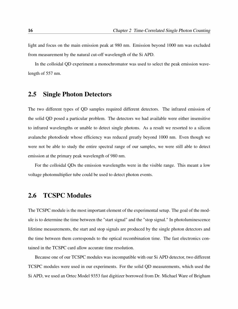
2.5 Single Photon Detectors
The two different types of QD samples required different detectors. The infrared emission of
the solid QD posed a particular problem. The detectors we had available were either insensitive
to infrared wavelengths or unable to detect single photons. As a result we resorted to a silicon
avalanche photodiode whose efficiency was reduced greatly beyond 1000 nm. Even though we
were not be able to study the entire spectral range of our samples, we were still able to detect
emission at the primary peak wavelength of 980 nm.
For the colloidal QDs the emission wavelengths were in the visible range. This meant a low
voltage photomultiplier tube could be used to detect photon events.
2.6 TCSPC Modules
The TCSPC module is the most important element of the experimental setup. The goal of the mod-
ule is to determine the time between the "start signal" and the "stop signal." In photoluminescence
lifetime measurements, the start and stop signals are produced by the single photon detectors and
the time between them corresponds to the optical recombination time. The fast electronics con-
tained in the TCSPC card allow accurate time resolution.
Because one of our TCSPC modules was incompatible with our Si APD detector, two different
TCSPC modules were used in our experiments. For the solid QD measurements, which used the
Si APD, we used an Ortec Model 9353 fast digitizer borrowed from Dr. Michael Ware of Brigham

2.6 TCSPC Modules 17
Young University. For the colloidal QD measurements we used an Edinburgh Instruments TCC900
TCSPC card. The settings used for each of the two experiments can be found in appendix A.
2.6.1 Ortec Model 9353 Fast Digitizer
The Ortec Model 9353 fast digitizer is the simpler of the two TCSCP modules we used. It uses a
10 GHz internal clock to produce a time stamp for each pulse and compares the time stamps of the
start and stop signals. This mode of operation is referred to as "time of flight mode" (TOF). In TOF
mode, the Model 9353 can produce up to 100 ps time resolution. This resolution is not as high as
the Edinburgh Instruments TCSPC card, however, the Edinburgh Instruments TCC900 required a
negative voltage pulse from the detector. The Si APD produced positive voltage peaks in response
to emitted photons and therefore could not be used to trigger the TCC900 card. The Ortec Model
9353 could be triggered by either positive or negative peaks and was therefore used in the InGaAs
QD measurements.
2.6.2 Edinburgh Instruments TCC900
The Edinburgh Instruments TCC900 TCSPC card uses a more complicated system of electronics
to obtain more accurate time resolution. This card was able to achieve a maximum resolution of 1
ps. This increase in resolution is possible because of the three main components of the TCC900;
the constant fraction discriminator (CFD), the time to amplitude converter (TAC), and the analog
to digital converter (ADC).
Like the Ortec Model 9353, the TCC900 is triggered with a start pulse and a stop pulse from the
photon detectors. The signals first pass the CFD which replaces the more typical threshold trigger.
In many other systems, including the Ortec fast digitizer, a pulse is detected when the voltage
reaches a certain threshold level. This method can introduce a small amount of error, called "time
walk" in the timing of the trigger if the pulses do not have a uniform amplitude (see Fig. 2.3). For

18 Chapter 2 Time-Correlated Single Photon Counting
Puls
e H
eight
Time
Time Walk
Threshold
Figure 2.3 This figure shows the inherent temporal uncertainty of threshold triggers. Thepeaks of both pulses arrive at the same time, but the pulse with a larger amplitude reachesthe threshold faster than the small pulse. This phenomenon is known as "time walk."
example, a large peak will reach the threshold slightly faster than small peak and therefore trigger
slightly sooner. A CFD, on the other hand, accounts for variations in amplitude by triggering once
the pulse has reached a certain fraction of its amplitude. Because the pulse shape is the same for
each pulse, even if the amplitude varies, the time to reach this fractional threshold will be the same.
The result is more precise definition of when the pulse occurred.
Once the CFD of the start signal path has been triggered, the time to amplitude converter begins
measuring the time until the "stop" signal is received. Triggering the TAC begins the charging of
a capacitor. Because of the well-defined relationship of charge on a capacitor vs. time, this can
be used to accurately measure the time between signals. For photoluminescence lifetime measure-
ments, the time between signals corresponds to the time between excitation and recombination.
When a pulse is received at the "stop" input the charge on the TAC is measured and passed
to the analog to digital converter. The ADC uses the time dependence of the capacitor to deter-
mine the recombination time of the detected photon. The ADC resolves the measurement time
into very small time intervals. The detected photon is counted in the interval corresponding to
2.7 Cryostat 19
its measured recombination time. The software of the TCSPC card can then create a histogram
displaying the number of photons counted in each interval vs. that interval’s corresponding time
after excitation. Because the intensity is proportional to the number of photons this equates to a
plot of photoluminescence intensity over time.
2.7 Cryostat
The photoluminescence of the solid QDs is typically dependent on their temperature. The pho-
toluminescence spectra of the samples used in this study showed strong temperature dependence
(ref. Jones et al. [19]). For this reason the solid QDs were mounted to the cold finger of a Cryo
Industries closed-cycle helium cryostat. Exterior windows allowed optical access to the samples
through which we excited them and collected photoluminescence. Samples were measured at 4 K.
2.8 CdSe QD Specific Equipment
The CdSe QDs required excitation at a wavelength below 500 nm. The laser pulses from our
Ti:Sapph laser were centered at 800 nm so a frequency-doubling, nonlinear crystal was used to
produce excitation at 400 nm.
The photoluminescence lifetimes of the colloidal QDs were much longer than the repetition
rate of the laser. This meant that the photoluminescence did not decay back to baseline levels
before the arrival of the next excitation pulse. The peaks would simply build upon each other so
that only the early part of the decay curve was distinguishable while the latter part was hidden by
subsequent peaks.
In order to observe the latter end of the photoluminescence decay we added an acousto-optic
modulator (AOM) to the excitation beam. The AOM acted as a fast shutter to block pulses and
allow the photoluminescence to decay fully. However, the AOM was not fast enough to allow one

20 Chapter 2 Time-Correlated Single Photon Counting
pulse through at a time. The functional limit of the AOM was about 100 ns which corresponds to
5-6 excitation pulses. The duty cycle of the AOM could be adjusted to allow the last excitation to
fully decay before the next series of pulses, allowing us to measure the photoluminescence lifetime
of the last pulse.
2.9 Impulse Response Function
Previous lifetime measurements of InGaAs QDs [8] led us to expect lifetimes on the order of one
nanosecond. We knew this would approach the limits of our Si APD so we decided to measure the
instrument’s response to scattered laser light. The pulse width of the laser was 30 fs which is five
orders of magnitude shorter than the expected lifetimes. This gave us an adequate approximation
to a delta function in order to measure the impulse response function (IRF) of our detector.
The laser light was focused onto a portion of the sample area that was not covered by a sample.
Scattered light was collected and focused into the detector as described above, and a lifetime mea-
surement was taken. The result was a luminescence decay curve similar in shape to our sample
measurements. The lifetime of that curve represented our instrument response time and was deter-
mined to be about 1 ns. The measured data for our InGaAs QD samples was only slightly longer
than this, with lifetimes of approximately 1.7 ns.
We concluded that our measured data must be a convolution of the impulse response function
with the real photoluminescence lifetime. In order to determine the true photoluminescence life-
time of our samples we would need to perform a deconvolution on each data set. The results of our
deconvolution calculations are in section 3.2.

Chapter 3
Results and Discussion
3.1 Expected Results
Previous studies have shown that InGaAs QDs grown on GaAs substrates have photoluminescence
lifetimes of about 1 ns [8]. Other QD structures including QD chains and QDs grown in close
proximity to quantum wells have shown that the photoluminescence lifetimes are lengthened in
these structures [20]. In order for recombination to occur the excited electron must interact with the
hole in the valence band. In highly confined structures, like quantum dots, this happens quickly. In
coupled systems the electrons and holes can move farther apart and therefore recombination times
are lengthened.
The modified Stranski-Krastanov growth method used to grow our InGaAs QDs has been
shown to create QD chains [13]. We, therefore, were expecting to measure lifetimes slightly longer
than the previously published lifetimes for isolated QDs.
For our colloidal QD samples we expected exponential decay curves with lifetimes of between
5 ns and 25 ns.
21
22 Chapter 3 Results and Discussion
3.2 Deconvolution
After comparing the measurements performed on our solid QD samples to the impulse response
function of our Si APD detector, we concluded that deconvolution would be necessary to determine
the actual value of the photoluminescence lifetimes. Using this technique we were able to measure
short lifetimes between 0.6 ns and 1 ns for our InGaAs QDs even though our impulse response was
as large as 1 ns.
The measurements we took were a convolution of the real photoluminescence decay with the
impulse response function (IRF). The similarity of the measured lifetimes to the IRF meant that the
convolution was non-negligible. In order to accurately determine the real photoluminescence life-
time we would have to deconvolve the two. The convolution theorem shown in Eqn. 3.1 indicates
that analysis of the data can be done by taking the Fourier transform of the data.
F [h] = F [ f ⊗g] = F [ f ]×F [g] (3.1)
In this equation h represents the data that we measured, f represents the real photoluminescence
decay, g is the impulse response function, F indicates the Fourier transform, and f ⊗g represents
the convolution of f with g. In Fourier space the measured data, which is a convolution of the real
measurement with the IRF, is a product of the two. The measured data can then be divided by the
IRF and the inverse Fourier transform calculated to deconvolve the real decay as shown in Eqn. 3.2
(where F−1 indicates the inverse Fourier transform).
f = F−1[F [h]F [g]
] (3.2)
As shown in Fig. 3.1 our solid QD data was a series of peaks and decays coinciding with the 82
MHz repetition rate of our pulsed laser. For each sample and experimental parameter one of those
peaks was chosen to be used in the analysis. Note the uniformity of the peaks in Fig. 3.1, so this
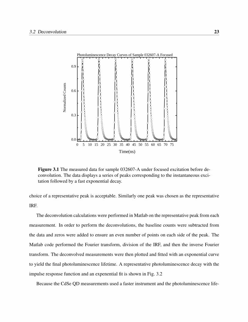
3.2 Deconvolution 23
0 5 10 15 20 25 30 35 40 45 50 55 60 65 70 750.0
0.3
0.6
0.9
Nor
mal
ized
Cou
nts
Time(ns)
Photoluminescence Decay Curves of Sample 032607-A Focused
Figure 3.1 The measured data for sample 032607-A under focused excitation before de-convolution. The data displays a series of peaks corresponding to the instantaneous exci-tation followed by a fast exponential decay.
choice of a representative peak is acceptable. Similarly one peak was chosen as the representative
IRF.
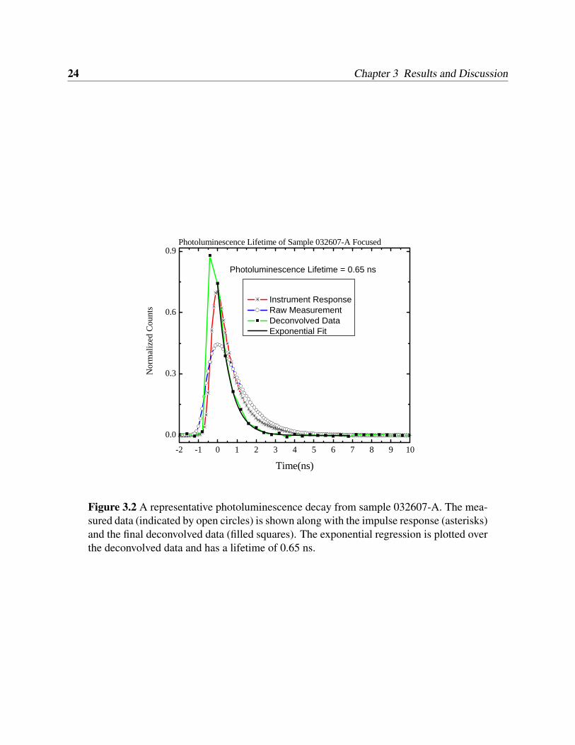
The deconvolution calculations were performed in Matlab on the representative peak from each
measurement. In order to perform the deconvolutions, the baseline counts were subtracted from
the data and zeros were added to ensure an even number of points on each side of the peak. The
Matlab code performed the Fourier transform, division of the IRF, and then the inverse Fourier
transform. The deconvolved measurements were then plotted and fitted with an exponential curve
to yield the final photoluminescence lifetime. A representative photoluminescence decay with the
impulse response function and an expenential fit is shown in Fig. 3.2
Because the CdSe QD measurements used a faster instrument and the photoluminescence life-
24 Chapter 3 Results and Discussion
-2 -1 0 1 2 3 4 5 6 7 8 9 10
0.0
0.3
0.6
0.9
Instrument Response Raw Measurement Deconvolved Data Exponential Fit
Nor
mal
ized
Cou
nts
Time(ns)
Photoluminescence Lifetime of Sample 032607-A Focused
Photoluminescence Lifetime = 0.65 ns
Figure 3.2 A representative photoluminescence decay from sample 032607-A. The mea-sured data (indicated by open circles) is shown along with the impulse response (asterisks)and the final deconvolved data (filled squares). The exponential regression is plotted overthe deconvolved data and has a lifetime of 0.65 ns.
3.3 InGaAs Quantum Dots 25
times were longer, the deconvolution technique was not needed.
3.3 InGaAs Quantum Dots
Samples were named according to the date on which they were grown with A or B indicating the
first or second sample grown that day. Thus sample 032607-A was the first of two samples grown
March 26, 2007. These samples were excited by a 9 mW beam that was first unfocused and then
focused on the sample. A summary of all of the InGaAs QD photoluminescence lifetimes is found
in Table 3.1.
Sample Unfocused
Lifetime
Focused
Lifetime
032607-A 0.78 ns 0.65 ns
032607-B 0.86 ns 0.78 ns
032907 0.96 ns 0.60 ns
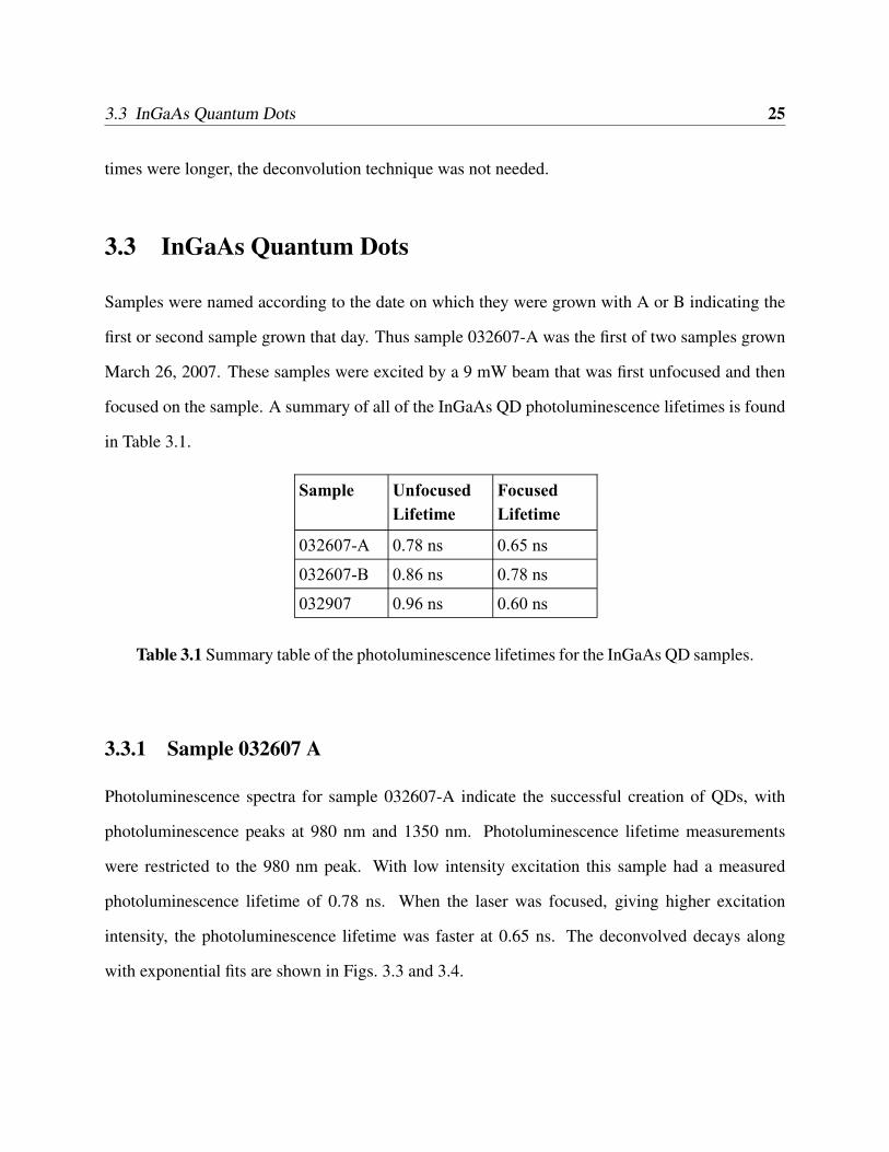
Table 3.1 Summary table of the photoluminescence lifetimes for the InGaAs QD samples.
3.3.1 Sample 032607 A
Photoluminescence spectra for sample 032607-A indicate the successful creation of QDs, with
photoluminescence peaks at 980 nm and 1350 nm. Photoluminescence lifetime measurements
were restricted to the 980 nm peak. With low intensity excitation this sample had a measured
photoluminescence lifetime of 0.78 ns. When the laser was focused, giving higher excitation
intensity, the photoluminescence lifetime was faster at 0.65 ns. The deconvolved decays along
with exponential fits are shown in Figs. 3.3 and 3.4.

26 Chapter 3 Results and Discussion
-2 -1 0 1 2 3 4 5 6 7 8 9 10
0.0
0.3
0.6
0.9
Deconvolved Data Exponential Fit
Nor
mal
ized
Cou
nts
Time(ns)
Photoluminescence Lifetime of Sample 032607-A Focused
Photoluminescence Lifetime = 0.65 ns
Figure 3.3 Photoluminescence decay of sample 032607-A with a focused excitationbeam. The photoluminescence lifetime is 0.65 ns.
-2 0 2 4 6 8 100.0
0.2
0.4
0.6
0.8
1.0
Deconvolved Data Exponential Fit
Nor
mal
ized
Cou
nts
Time(ns)
Photoluminescence Lifetime of Sample 032607-A Unfocused
Photoluminescence Lifetime = 0.78 ns
Figure 3.4 Photoluminescence decay of sample 032607-A with an unfocused excitationbeam. The photoluminescence lifetime is 0.78 ns.
3.3 InGaAs Quantum Dots 27
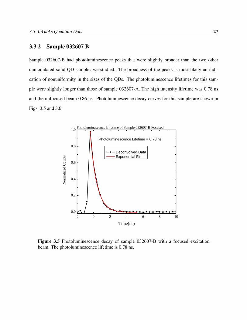
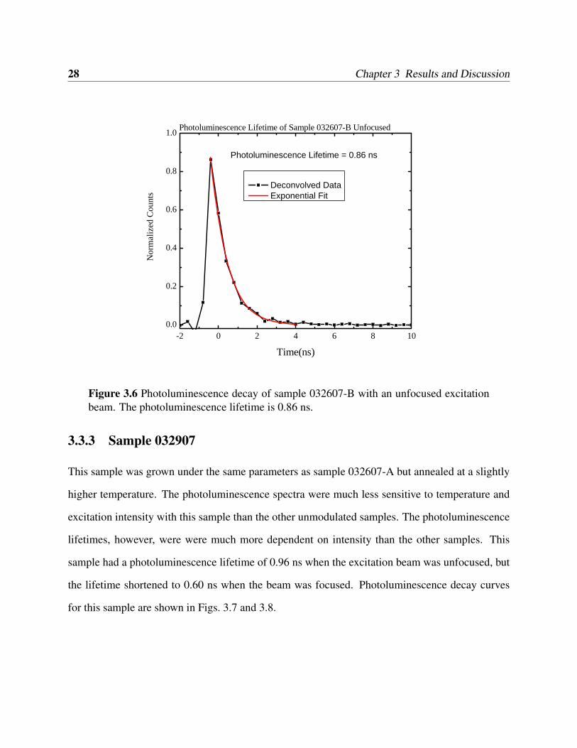
3.3.2 Sample 032607 B
Sample 032607-B had photoluminescence peaks that were slightly broader than the two other
unmodulated solid QD samples we studied. The broadness of the peaks is most likely an indi-
cation of nonuniformity in the sizes of the QDs. The photoluminescence lifetimes for this sam-
ple were slightly longer than those of sample 032607-A. The high intensity lifetime was 0.78 ns
and the unfocused beam 0.86 ns. Photoluminescence decay curves for this sample are shown in
Figs. 3.5 and 3.6.
-2 0 2 4 6 8 100.0
0.2
0.4
0.6
0.8
1.0
Deconvolved Data Exponential Fit
Nor
mal
ized
Cou
nts
Time(ns)
Photoluminescence Lifetime of Sample 032607-B Focused
Photoluminescence Lifetime = 0.78 ns
Figure 3.5 Photoluminescence decay of sample 032607-B with a focused excitationbeam. The photoluminescence lifetime is 0.78 ns.
28 Chapter 3 Results and Discussion
-2 0 2 4 6 8 100.0
0.2
0.4
0.6
0.8
1.0
Deconvolved Data Exponential Fit
Nor
mal
ized
Cou
nts
Time(ns)
Photoluminescence Lifetime of Sample 032607-B Unfocused
Photoluminescence Lifetime = 0.86 ns
Figure 3.6 Photoluminescence decay of sample 032607-B with an unfocused excitationbeam. The photoluminescence lifetime is 0.86 ns.
3.3.3 Sample 032907
This sample was grown under the same parameters as sample 032607-A but annealed at a slightly
higher temperature. The photoluminescence spectra were much less sensitive to temperature and
excitation intensity with this sample than the other unmodulated samples. The photoluminescence
lifetimes, however, were were much more dependent on intensity than the other samples. This
sample had a photoluminescence lifetime of 0.96 ns when the excitation beam was unfocused, but
the lifetime shortened to 0.60 ns when the beam was focused. Photoluminescence decay curves
for this sample are shown in Figs. 3.7 and 3.8.

3.3 InGaAs Quantum Dots 29
-2 0 2 4 6 8 100.0
0.2
0.4
0.6
0.8
1.0
Deconvolved Data Exponential Fit
Nor
mal
ized
Cou
nts
Time(ns)
Photoluminescence Lifetime of Sample 032907 Focused
Photoluminescence Lifetime = 0.60 ns
Figure 3.7 Photoluminescence decay of sample 032907 with a focused excitation beam.The photoluminescence lifetime is 0.60 ns.
-2 0 2 4 6 8 100.0
0.2
0.4
0.6
0.8
1.0
Deconvolved Data Exponential Fit
Nor
mal
ized
Cou
nts
Time(ns)
Photoluminescence Lifetime of Sample 032907 Unfocused
Photoluminescence Lifetime = 0.96 ns
Figure 3.8 Photoluminescence decay of sample 032907 with an unfocused excitationbeam. The photoluminescence lifetime is 0.96 ns.

30 Chapter 3 Results and Discussion
3.4 CdSe Quantum Dots
The colloidal samples measured exhibited multiple exponential decays, typically a fast decay fol-
lowed by a slower one. In order to study this we performed high resolution short lifetime mea-
surements as well as lower resolution longer lifetime measurements. The limitations of our AOM
prevented us from reducing the duty cycle of the excitation to a single pulse. As a result the later
portion of the photoluminescence decay was observed by allowing a series of 4-5 pulses to excite
the sample and then observing the decay after the final pulse. The short measurements were per-
formed by analyzing only the first few nanoseconds of the decay. Because the repetition rate of the
pulsed laser was much faster than the decay time of the sample, the photoluminescence could not
fully decay before the next excitation. Enough decay had occurred, however, to allow analysis of
the early part of the decay curve.
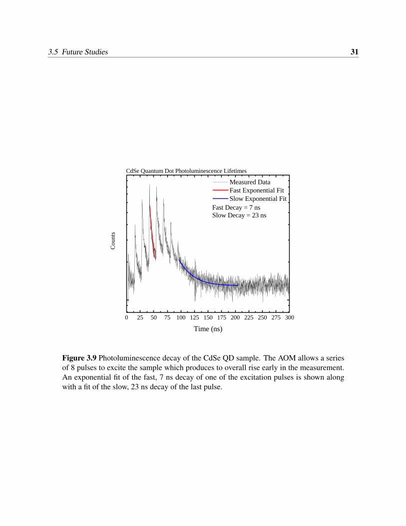
Figure 3.9 demonstrates the fast and slow decay curves of the CdSe sample. In this figure a
series of 8 pulses is allowed to excite the sample followed by a long decay period. The fast lifetime
can be determined by fitting an exponential curve to one of the early peaks. This yielded a lifetime
of 7 ns. To find the slow photoluminesence lifetime we focused on the late portion of the last peak.
An exponential fit of this region showed that the slow lifetime was 23 ns. The exponential fits for
these regions can be seen in Fig. 3.9.
3.5 Future Studies
Each of the solid QD samples displayed faster photoluminescence lifetimes when the intensity was
increased. This indicates the potential for future studies investigating the intensity dependence of
the photoluminescence lifetime. In addition, our detector limited the wavelengths that we were
able to study. Further studies could include lifetime measurements at many different wavelengths,
though wavelengths beyond 1000 nm would require a different detector.
3.5 Future Studies 31
0 25 50 75 100 125 150 175 200 225 250 275 300
Slow Decay = 23 ns
Measured Data Fast Exponential Fit Slow Exponential Fit
Cou
nts
Time (ns)
CdSe Quantum Dot Photoluminescence Lifetimes
Fast Decay = 7 ns
Figure 3.9 Photoluminescence decay of the CdSe QD sample. The AOM allows a seriesof 8 pulses to excite the sample which produces to overall rise early in the measurement.An exponential fit of the fast, 7 ns decay of one of the excitation pulses is shown alongwith a fit of the slow, 23 ns decay of the last pulse.
32 Chapter 3 Results and Discussion
The cryostat used for the solid QD measurements is capacle of controlling temperatures be-
tween 4 K and 300 K. Therefore, future studies could also include photoluminescence lifetime
measurement at various temperatures.
Finally, the collaborator who grew our current InGaAs QD samples, Dr. Yang, has grown a new,
laser-modulated InGaAs QD sample. A laser diffraction pattern was used to heat some areas of the
gallium arsenide substrate during epitaxial growth. Since the formation of QDs is highly dependent
on the temperature during growth, QDs were preferentially formed in the destructive interference
fringes of the diffraction pattern where no heating occurred. As a result, alternating areas of high
and low QD density are apparent on the surface of the sample. Preliminary photoluminescence
spectra of this sample have already been measured, and lifetime measurements will follow.

Appendix A
TCSPC Module Parameters
A.1 Edinburgh Instruments TCC900
A.1.1 Pulse Generator
The Edinburgh Instruments TCC900 module required creative use of an Agilent 8110A pulse gen-
erator to generate a suitable stream of reference pulses. Our pulsed Ti:Sapph laser operated at a
repetition rate of 82 MHz. The laser pulses were detected by an avalanche photodiode internal to
the laser cavity which produced positive amplitude pulses. These two characteristics were incom-
patible with the TCC900 card, which required negative pulses and a repetition rate below 10 MHz.
The pulse generator was used to reduce the repetition rate of the reference stream and invert the
output amplitude. It was also used to trigger the AOM responsible for creating packets of optical
pulses to excite the sample.
The pulse generator was operated in "triggered pulses" mode with the output of the photodi-
ode connected to the external trigger. The channel 1 output was set to an appropriate level for
the TCC900. This was done using a high voltage of 0 V and a low voltage of -0.6 V. The de-
lay and pulse width were then adjusted to, respectively, reduce the repetition rate and center the
33

34 Chapter A TCSPC Module Parameters
measurement on the measurement window.
A.1.2 Measurement Window
Both the TCC900 and the Ortec Model 9353 took measurements inside a predetermined measure-
ment window. In other words, a time range had to be selected before each measurement. That
range was then divided into bins which determined the resolution of the measurement. For the
TCC900 the time range and number of channels were selected in the "Manual Measurement" di-
alog box (see Fig. A.1(a)). The CdSe QD measurements were taken with windows of 50 ns, 200
ns, and 500 ns. The number of channels used varied between 512 and 4096. The resolution was
determined by dividing the time window by the number of channels used. For example, a 50 ns
scan with 1024 channels corresponds to a time resolution of 49 ps/point. Occasionally, a bug in the
time settings would cause a mismatch between the data and the time scale. When this occurred the
photoluminescence peaks were compressed together. Changing time scales was typically sufficient
to alleviate the error.
The beginning of the measurement window is determined by the reference pulse. Extra delays
that were a result of differences in the cable lengths and the optical path lengths often caused the
excitation and luminescence decay curves to be shifted temporally relative to the reference pulse.
When this happened, the region of interest was not entirely visible in the measurement window.
The "Delay" parameter found in the "Time Range Settings" tab of the "TCC900 Options" dialog
box (see Fig. A.1(c)) is designed to compensate for this effect, but we had little success in using it
consistently. Instead, pulse generator settings were used to adjust the measurement temporally.
With the pulse generator triggered by the laser through the internal APD, both channels were set
to the same delay in order to fix the overall repetition period of our experiment.. Our measurements
were typically performed with a delay setting of 300 ns, corresponding to a repetition rate of 3.3
MHz. This means the TCC900 would receive reference signals at a rate of 3.3 MHz instead of 82

A.1 Edinburgh Instruments TCC900 35
(a) Manual Measurements (b) Options: CFD
(c) Options: Time Range Settings (d) Options: Mode
Figure A.1 Important dialog windows for the Edinburgh Instruments TCC900
MHz, which was necessary due to the cards’s 10 MHz limitation. Triggers that occurred during the
300 ns delay were ignored by the pulse generator, so the overall repetition rate was not interrupted.
The AOM was controlled at this same rate producing one packet of excitation pulses every 300 ns.
The width of the reference pulses was then adjusted so that the excitation packet arrived sooner
or later relative to the reference pulse. In this way we could shift the excitation packet and the
36 Chapter A TCSPC Module Parameters
decay curves to the left or right of the measurement window in order to measure the entire region
of interest.
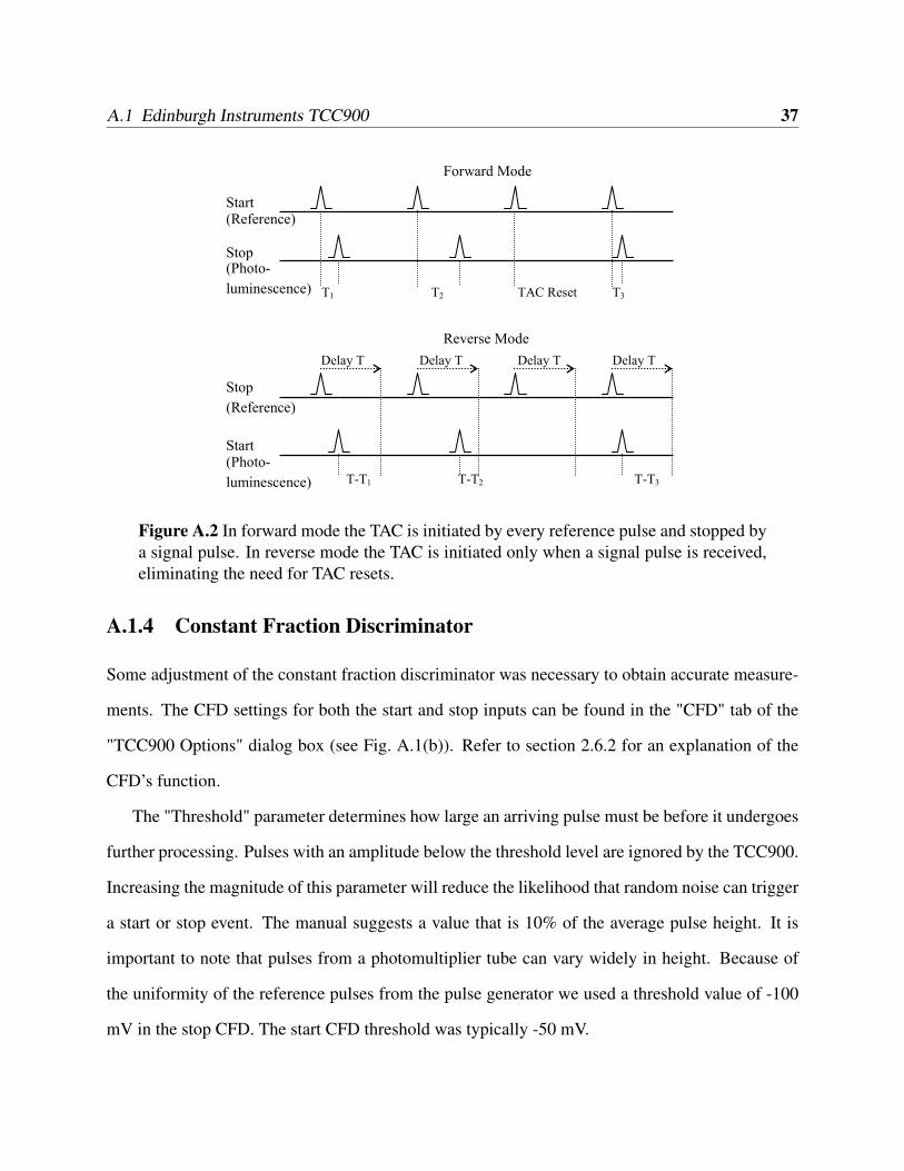
A.1.3 Forward and Reverse Modes
The TCC900 can operate in either forward or reverse mode. Switching between these two modes
can be done in the "Mode" tab of the "TCC900 Options" dialog box (see Fig. A.1(d)). The forward
mode is simpler and operates as described in section 2.1. Operating this way the reference pulses
must be connected to the "Start" input of the TCC900 and the photoluminescence signal must be
connected to the "Stop" input.
The reverse mode does the opposite, using the photoluminescence to trigger the start pulses and
the reference pulses to create stop signals. A predetermined, constant delay follows each reference
pulse. When the photoluminescence creates a start pulse, the TAC measures the time until the end
of the delay. By subtracting the measured time from the constant delay time, the photon’s arrival
time can be deduced.The software provided with the TCC900 automatically adjusts the data so
that the times reported in reverse mode reflect the time after excitation and not the time until the
next stop signal. Because the photoluminescence is filtered down so that only 1 in 1000 excita-
tions produce a photon at the detector, reverse mode has the advantage that the time to amplitude
converter is only activated when there is a start pulse. By eliminating the need for the TAC to reset
every cycle, the maximum number of counts processed can be increased by as much as a factor of
20. This translates to higher repetition rates and faster scan times. For this reason our CdSe QD
measurements were typically performed in reverse mode. Figure A.2 shows the difference between
forward and reverse modes of operation.
A.1 Edinburgh Instruments TCC900 37
Forward Mode
Start
Stop
Stop
Start
Reverse Mode
Delay T Delay T Delay T
T3 T2 T1 TAC Reset
T-T1
Delay T
T-T2 T-T3
(Reference)
(Reference)
(Photo-
luminescence)
(Photo-
luminescence)
Figure A.2 In forward mode the TAC is initiated by every reference pulse and stopped bya signal pulse. In reverse mode the TAC is initiated only when a signal pulse is received,eliminating the need for TAC resets.
A.1.4 Constant Fraction Discriminator
Some adjustment of the constant fraction discriminator was necessary to obtain accurate measure-
ments. The CFD settings for both the start and stop inputs can be found in the "CFD" tab of the
"TCC900 Options" dialog box (see Fig. A.1(b)). Refer to section 2.6.2 for an explanation of the
CFD’s function.
The "Threshold" parameter determines how large an arriving pulse must be before it undergoes
further processing. Pulses with an amplitude below the threshold level are ignored by the TCC900.
Increasing the magnitude of this parameter will reduce the likelihood that random noise can trigger
a start or stop event. The manual suggests a value that is 10% of the average pulse height. It is
important to note that pulses from a photomultiplier tube can vary widely in height. Because of
the uniformity of the reference pulses from the pulse generator we used a threshold value of -100
mV in the stop CFD. The start CFD threshold was typically -50 mV.
38 Chapter A TCSPC Module Parameters
The temporal position of the pulse is determined by finding the steepest slope of the initial
edge of the pulse. The "Fraction" and "Zero Crossing Level" parameters are used to optimize
which portion of the slope is taken to be this steepest slope. Another parameter, the "Constant
Fraction Delay," cannot be optimized by the software, but can be changed by inserting different
delay circuits into the hardware of the TCC900 card itself. These TCSPC data did not appear to
depend heavily on these parameters.. Adequate measurements were taken with a variety of settings
including the suggested values of 20% fraction and -5 mV zero crossing level. Our measurements
were typically taken with a 20% fraction and a -3 mV zero crossing level.
A.2 Ortec Model 9353 Fast Digitizer
The Ortec Model 9353 fast digitizer is much more simple to operate than the Edinburgh Instru-
ments TCC900 card. With a 10 GHz internal clock, the card can be triggered at a rate of 82 MHz,
and the inputs accept both positive and negative pulses. This means that there is no need for the
pulse generator. There is also no option to run the Model 9353 in reverse mode.
This card was operated exclusively in "Time of Flight" (TOF) mode for our InGaAs QD mea-
surements. This mode of operation is similar to the forward mode of the TCC900. See section 2.6.1
for greater explanation of this mode. The other mode of operation, "Chromat/Trend" mode, takes
multiple TOF scans and tracks changes in the number of stop events over larger periods of time.
This mode could be useful if, for example, the overall intensity of the signal was being modulated
on a time scale much longer than the time of an individual TOF scan.
Like the TCC900, the measurement window for the Model 9353 has to be determined before
the scan begins. This is done in the "Time of Flight mode" tab of the "Measurement Settings"
dialog box. The time span field can accept a continuous range from 51.2 ns to 6.7 ms. Instead of
choosing the number of bins, the user selects the desired time width of the bin with a minimum
A.2 Ortec Model 9353 Fast Digitizer 39
resolution of 100 ps. For our solid QD scans we used a time span of 200 ns with a resolution of
100 ps. Extra reference pulses included in the 200 ns span were ignored by the Model 9353 and
did not affect the measurement. The result was a time window that was triggered from the first
start pulse and included as many as 17 excitation and decay cycles before resetting 200 ns later.
Because the Model 9353 does not use a constant fraction discriminator to determine the the
temporal location of the incoming pulses, there are fewer settings to optimize. The Model 9353
allows the user to set the threshold levels on both the start and stop inputs as well as decide whether
the input triggers on the falling edge or rising edge of the pulse. These values can be set automati-
cally by the software using the "Auto Find" option, however, we typically set these levels manually
for our experiments. Our measurements were taken with a stop threshold of -0.3 mV triggered on
the falling edge and a start threshold of -0.34 mV triggered on the rising edge. These parameters
are found in the "General" tab of the "Measurement Settings" dialog box.

Bibliography
[1] P. Bhattacharya, S. Ghosh, and A. Stiff-Roberts, “Quantum Dot Opto-Electronic Devices,”
Annu. Rev. Mater. Res. 34, 1–40 (2004).
[2] H. Liu, M. Gao, J. McCaffrey, Z. Wasilewski, and S. Fafard, “Quantum Dot Infrared Pho-
todetectors,” Applied Physics Letters 78, 79–81 (2001).
[3] V. Egorov, G. Cirlin, N. Polyakov, V. Petrov, A. Tonkikh, B. Volovik, Y. Musikhin, A. Zhukov,
A. Tsatsulnikov, and V. Ustinov, “1.3-1.4 µm Photoluminescence Emission From InAs/GaAs
Quantum Dot Multilayer Structures Grown on GaAs Singular and Vicinal Substrates,” Nan-
otechnology 11, 323–327 (2000).
[4] P. Anikeeva, J. Halpert, M. Bawendi, and V. Bulovic, “Quantum Dot Light-Emitting Devices
with Electroluminescence Tunable over the Entire Visible Spectrum,” Nano Letters 9, 2532–
2536 (2009).
[5] S. H. Pyun, S. H. Lee, and I. C. Lee, “Photoluminescence and lasing characteristics of In-
GaAs/InGaAsP/InP quantum dots,” Journal of Applied Physics 96, 5766–5770 (2004).
[6] K. Prabakar, S. Minkyu, and S. Inyoung, “CdSe quantum dots co-sensitized TiO2 photoelec-
trodes:particle size dependent properties,” Journal of Physics D, Applied Physics 43, 012002–
1–012002–4 (2010).
41
42 BIBLIOGRAPHY
[7] T. Campbell-Ricketts, N. A. J. M. Kleemans, and R. Notzel, “The role of dot height in deter-
mining exciton lifetimes in shallow InAs/GaAs quantum dots,” Applied Physics Letters 96,
033102–1 (2010).
[8] Y. I. Mazur, B. H. Liang, and Z. M. Wang, “Time-resolved photoluminescence spectroscopy
of subwetting layer states in InGaAs/GaAs quantum dot structures,” Journal of Applied
Physics 100, 054316–1–054316–5 (2006).
[9] C. Y. Ngo, S. F. Yoon, and D. R. Lim, “Temperature-dependent photoluminescence study of
1.3 mm undoped InAs/InGaAs/GaAs quantum dots,” Applied Physics Letters 93, 041912–
041912 (2008).
[10] M. Syperek, P. Leszczynski, and J. Misiewicz, “Time-resolved photoluminescence spec-
troscopy of an InGaAs/GaAs quantum well-quantum dots tunnel injection structure,” Applied
Physics Letters 96, 011901–1 (2010).
[11] S. Bose, “Quantum Communication through an Unmodulated Spin Chain,” Physical Review
Letters 91, 1–4 (2003).
[12] W. Chang, T. Hsu, K. Tsai, T. Nee, J. Chyi, and N. Yeh, “Excitation Density and Temperature
Dependent Photoluminescence of InGaAs Self-Assembled Quantum Dots,” Japanese Journal
of Applied Physics 38, 554–557 (1999).
[13] D. Kim and H. Yang, “Shape Control of InGaAs Nanostructures on Nominal GaAs(001):
Dashes and Dots,” Nanotechnology 19, 1–5 (2008).
[14] J. Lee, Z. Wang, B. Liang, W. Black, V. Kunets, Y. Mazur, and G. Salamo, “Selective Growth
of InGaAs/GaAs Quantum Dot Chains on Pre-Patterned GaAs(001),” Nanotechnology 17,
2275–2278 (2006).

BIBLIOGRAPHY 43
[15] V. Turck, F. Heinrichsdorff, M. Veit, R. Heitz, M. Grundmann, A. Krost, and D. Bimberg,
“Correlation of InGaAs/GaAs Quantum Dot and Wetting Layer Formation,” Applied Surface
Science 123, 352–355 (1998).
[16] Z. Wang, K. Holmes, Y. Mazur, and G. Salamo, “Fabrication of (In,Ga)As Quantum-Dot
Chains on GaAs(100),” Applied Physics Letters 84, 1931–1933 (2004).
[17] G. Slepyan, Y. Yerchak, A. Hoffman, and F. Bass, “Strong Electron-Photon Coupling in a On-
Dimensional Quantum Dot Chain: Rabi Waves and Rabi Wave Packets,” Physical Review B
81, 1–18 (2010).
[18] S. Mirabella, R. Agosta, G. Franzo, I. Crupi, M. Miritello, R. L. Savio, M. D. Stefano, S. D.
Marco, and A. Terrasi, “Light Absorption in Silicon Quantum Dots Embedded in Silica,”
Journal of Applied Physics 106, 103505–1–103505–8 (2010).
[19] A. Jones, “Photoluminescence of Indium Gallium Arsenide Quantum Dots and Dot Chains,”
Brigham Young University Thesis (2010).
[20] Y. I. Mazur, B. H. Liang, Z. M. Wang, G. Tasarov, D. Guzun, and G. Salamo, “Lengthening
of the Photoluminescence Decay Time of InAs Quantum Dots Coupled to InGaAs/GaAs
Quantum Well,” Journal of Applied Physics 100, 054313–1–054313–4 (2006).


![arXiv:1403.7798v1 [cond-mat.mes-hall] 30 Mar 2014 binding energy, we can expect a fast exciton ra-diative decay. Recent reports showed photoluminescence (PL) lifetimes decreasing with](https://static.fdocuments.us/doc/165x107/5b1eb9857f8b9a22028bebaf/arxiv14037798v1-cond-matmes-hall-30-mar-2014-binding-energy-we-can-expect.jpg)


