
PGA900 Programmable Resistive Sensing Conditioner With ... · power management internal oscillator...
141
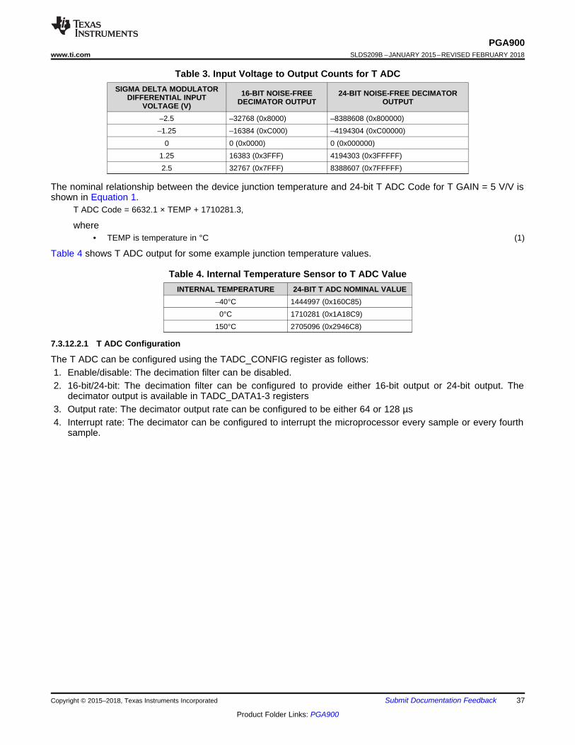
POWER MANAGEMENT INTERNAL OSCILLATOR DIAGNOSTICS SCL, SDA ARM CORTEX M0 (PROGRAMMABLE BY USERS) GAIN VDD (3.3 – 30 V) OWI SPI, UART I2C PWM VOUT MUX DEBUGGER INTERNAL TEMPERATURE SENSOR TOPDIG, TONDIG MISO/TX, MOSI/RX, CSN, SCK RATIOMETRIC BRIDGE EXCITATION 24-bit ADC PGA 24-bit ADC PGA CONTROL AND STATUS REGISTERS SOFTWARE AND DATA MEMORY EEPROM 14-bit DAC PGA900 VBRGP VBRGN VINPP VINPN VINTP VINTN OPTIONAL EXTERNAL TEMPERATURE SENSOR BRIDGE SENSOR TEMPERATURE SENSING AFE RESISTIVE SENSING AFE OR SWDIO, SWDCLK REFERENCE GPIO2 GPIO1 Product Folder Order Now Technical Documents Tools & Software Support & Community An IMPORTANT NOTICE at the end of this data sheet addresses availability, warranty, changes, use in safety-critical applications, intellectual property matters and other important disclaimers. PRODUCTION DATA. PGA900 SLDS209B – JANUARY 2015 – REVISED FEBRUARY 2018 PGA900 Programmable Resistive Sensing Conditioner With Digital and Analog Outputs 1 1 Features 1• High Accuracy, Low Noise, Low Power, Small Size Resistive Sensing Signal Conditioner • User-Programmable Temperature and Nonlinearity Compensation • On-Chip ARM ® Cortex ® M0 Microprocessor Allows Users to Develop and Implement Calibration Software • One-Wire Interface Enables the Communication through Power Supply Pin Without Using Additional Lines • On-Chip Power Management Accepts Wide Power Supply Voltage From 3.3 V to 30 V • Operating Temperature Range: –40°C to +150°C • Memory – 8 kB Software Memory – 128 Bytes EEPROM – 1 kB Data SRAM • Accommodates Sensor Sensitivities From 1 mV/V to 135 mV/ V • Two Individual Analog-Front End (AFE) Chains, Each Including: – Low Noise Programmable Gain Amplifier – 24-Bit Sigma-Delta Analog-to-Digital Converter • Built-In Internal Temperature Sensor With Option to Use External Temperature Sensor • 14-Bit DAC With Programmable Gain Amplifier • Output Options: – Ratiometric and Absolute Voltage Output – 4- to 20-mA Current Loop Interface – One-Wire Interface (OWI) Over Power Line – PWM Output – Serial Peripheral Interface (SPI) – Inter-Integrated Circuit (I 2 C) • Depletion MOSFET Gate Driver • Diagnostic Functions 2 Applications • Pressure Sensor Transmitters and Transducers • Liquid Level Meters and Flow Meters • Weight Scales, Load Meters, and Strain Gauges • Thermocouples, Thermistors, and 2-Wire Resistance Thermometers (RTD) • Resistive Field Transmitters 3 Description The PGA900 is a signal conditioner for resistive sensing applications. It can accommodate various sensing element types. The PGA900 conditions its input signals by amplification and digitization through two analog front end channels. With the user programmed software in the on-chip ARM Cortex M0 processor, the PGA900 can perform linearization, temperature compensation, and other user defined compensation algorithms. The conditioned signal can be output as ratiometric voltage, absolute voltage, 4- to 20-mA current loop or PWM. The data and configuration registers can also be accessed through SPI, I 2 C, UART, and two GPIO ports. In addition, the unique OWI allows communication and configuration through the power supply pin without using additional lines. The PGA900 operating voltage is from 3.3 V to 30 V and it can operate in temperatures from –40°C to +150°C. Device Information (1) PART NUMBER PACKAGE BODY SIZE (NOM) PGA900 VQFN (36) 6.00 mm × 6.00 mm DSBGA (36) 3.66 mm × 3.66 mm (1) For all available packages, see the orderable addendum at the end of the data sheet. PGA900 Simplified Block Diagram
Transcript of PGA900 Programmable Resistive Sensing Conditioner With ... · power management internal oscillator...

POWER MANAGEMENT
INTERNAL OSCILLATOR
DIAGNOSTICS
SCL, SDA
ARM CORTEX M0
(PROGRAMMABLE BY USERS)
GAIN
VDD (3.3 ± 30 V)
OWI
SPI,UART
I2C
PWM
VOUTMU
X
DEBUGGER
INTERNAL TEMPERATURE
SENSOR
TOPDIG, TONDIG
MISO/TX, MOSI/RX, CSN, SCK
RATIOMETRIC BRIDGE EXCITATION
24-bit ADC
PGA
24-bit ADC
PGA
CONTROL AND
STATUS REGISTERS
SOFTWARE AND DATA MEMORY
EEPROM
14-bit DAC
PGA900VBRGP
VBRGN
VINPP
VINPN
VINTP
VINTN
OPTIONAL EXTERNAL
TEMPERATURE SENSOR
BRIDGE SENSOR
TEMPERATURE SENSING AFE
RESISTIVE SENSING AFE
OR
SWDIO,SWDCLK
REFERENCE
GPIO2
GPIO1
Product
Folder
Order
Now
Technical
Documents
Tools &
Software
Support &Community
An IMPORTANT NOTICE at the end of this data sheet addresses availability, warranty, changes, use in safety-critical applications,intellectual property matters and other important disclaimers. PRODUCTION DATA.
PGA900SLDS209B –JANUARY 2015–REVISED FEBRUARY 2018
PGA900 Programmable Resistive Sensing Conditioner With Digital and Analog Outputs
1
1 Features1• High Accuracy, Low Noise, Low Power, Small
Size Resistive Sensing Signal Conditioner• User-Programmable Temperature and
Nonlinearity Compensation• On-Chip ARM® Cortex® M0 Microprocessor
Allows Users to Develop and ImplementCalibration Software
• One-Wire Interface Enables the Communicationthrough Power Supply Pin Without UsingAdditional Lines
• On-Chip Power Management Accepts WidePower Supply Voltage From 3.3 V to 30 V
• Operating Temperature Range: –40°C to +150°C• Memory
– 8 kB Software Memory– 128 Bytes EEPROM– 1 kB Data SRAM
• Accommodates Sensor Sensitivities From 1 mV/Vto 135 mV/ V
• Two Individual Analog-Front End (AFE) Chains,Each Including:– Low Noise Programmable Gain Amplifier– 24-Bit Sigma-Delta Analog-to-Digital Converter
• Built-In Internal Temperature Sensor With Optionto Use External Temperature Sensor
• 14-Bit DAC With Programmable Gain Amplifier• Output Options:
– Ratiometric and Absolute Voltage Output– 4- to 20-mA Current Loop Interface– One-Wire Interface (OWI) Over Power Line– PWM Output– Serial Peripheral Interface (SPI)– Inter-Integrated Circuit (I2C)
• Depletion MOSFET Gate Driver• Diagnostic Functions
2 Applications• Pressure Sensor Transmitters and Transducers• Liquid Level Meters and Flow Meters• Weight Scales, Load Meters, and Strain Gauges• Thermocouples, Thermistors, and 2-Wire
Resistance Thermometers (RTD)• Resistive Field Transmitters
3 DescriptionThe PGA900 is a signal conditioner for resistivesensing applications. It can accommodate varioussensing element types. The PGA900 conditions itsinput signals by amplification and digitization throughtwo analog front end channels. With the userprogrammed software in the on-chip ARM Cortex M0processor, the PGA900 can perform linearization,temperature compensation, and other user definedcompensation algorithms. The conditioned signal canbe output as ratiometric voltage, absolute voltage, 4-to 20-mA current loop or PWM. The data andconfiguration registers can also be accessed throughSPI, I2C, UART, and two GPIO ports. In addition, theunique OWI allows communication and configurationthrough the power supply pin without using additionallines. The PGA900 operating voltage is from 3.3 V to30 V and it can operate in temperatures from –40°Cto +150°C.
Device Information(1)
PART NUMBER PACKAGE BODY SIZE (NOM)
PGA900VQFN (36) 6.00 mm × 6.00 mmDSBGA (36) 3.66 mm × 3.66 mm
(1) For all available packages, see the orderable addendum atthe end of the data sheet.
PGA900 Simplified Block Diagram

2
PGA900SLDS209B –JANUARY 2015–REVISED FEBRUARY 2018 www.ti.com
Product Folder Links: PGA900
Submit Documentation Feedback Copyright © 2015–2018, Texas Instruments Incorporated
Table of Contents1 Features .................................................................. 12 Applications ........................................................... 13 Description ............................................................. 14 Revision History..................................................... 25 Pin Configuration and Functions ......................... 36 Specifications......................................................... 6
6.1 Absolute Maximum Ratings ...................................... 66.2 ESD Ratings.............................................................. 66.3 Recommended Operating Conditions....................... 66.4 Thermal Information .................................................. 76.5 Electrical Characteristics—Gate Drive...................... 86.6 Reverse Voltage Protection ...................................... 86.7 Regulators................................................................. 86.8 Internal Reference..................................................... 86.9 Internal Oscillator ..................................................... 86.10 Bridge Sensor Supply ............................................. 96.11 Temperature Sensor Supply ................................. 106.12 Internal Temperature Sensor ................................ 106.13 P Gain (Chopper Stabilized) ................................. 116.14 P Analog-to-Digital Converter ............................... 126.15 T Gain (Chopper Stabilized) ................................. 136.16 T Analog-to-Digital Converter ............................... 146.17 OWI ....................................................................... 146.18 SPI ........................................................................ 146.19 I2C Interface .......................................................... 156.20 PWM Output.......................................................... 156.21 DAC Output........................................................... 156.22 DAC Gain .............................................................. 156.23 GPIO, Digital Test In-Test Out, UART TX/RX
Buffers...................................................................... 18
6.24 Non-Volatile Memory............................................. 186.25 Diagnostics............................................................ 186.26 M0 ......................................................................... 206.27 OWI Timing Requirements.................................... 206.28 SPI Timing Requirements ..................................... 206.29 I2C Interface Timing Requirements....................... 226.30 Typical Characteristics .......................................... 23
7 Detailed Description ............................................ 257.1 Overview ................................................................. 257.2 Functional Block Diagram ....................................... 267.3 Feature Description................................................. 277.4 Device Functional Modes........................................ 717.5 Register Maps ......................................................... 72
8 Application and Implementation ...................... 1188.1 Application Information.......................................... 1188.2 Typical Applications .............................................. 118
9 Power Supply Recommendations .................... 12810 Layout................................................................. 128
10.1 Layout Guidelines ............................................... 12810.2 Layout Example .................................................. 128
11 Device and Documentation Support ............... 13011.1 Documentation Support ...................................... 13011.2 Receiving Notification of Documentation
Updates.................................................................. 13011.3 Community Resources........................................ 13011.4 Trademarks ......................................................... 13011.5 Electrostatic Discharge Caution.......................... 13011.6 Glossary .............................................................. 130
12 Mechanical, Packaging, and OrderableInformation ......................................................... 130
4 Revision HistoryNOTE: Page numbers for previous revisions may differ from page numbers in the current version.
Changes from Revision A (May 2015) to Revision B Page
• Added a new package to the Device Information table.......................................................................................................... 1• Added new YZS package drawing ......................................................................................................................................... 3• Changed minimum and nominal OTP programming voltages from 7.0 and 7.4 to 7.2 and 7.6............................................. 6• Added DSBGA thermal info.................................................................................................................................................... 7• Added statement related to waiting time before reading trace FIFO.................................................................................... 61• Replaced "Data" with "Development" ................................................................................................................................... 69• Fixed broken figure crossreference ...................................................................................................................................... 71• Replaced "PADC" with "TADC" ............................................................................................................................................ 86• Replaced "PADC" with "TADC" ............................................................................................................................................ 86• Fixed description for "0" state............................................................................................................................................. 109
Changes from Original (January 2015) to Revision A Page
• Updated device to production data......................................................................................................................................... 1
SCL
MISO/TX
MOSI/RX
SWDIO
GATE
AVDD
VDD
FBP
SDA
GPIO_1/TIPDIG
TIN/VEXTN
TIP/VEXTP
65431
54321
A
B
C
D
E
F
A
C
D
E
F
WCSP PACKAGE
TONDIG
GPIO_2/TINDIG
FBN
VINTP
AVSS VP_OTP
GND
VINPP
VINPN
DVDD_MEM
VOUT
VINTN
DVSS
DVDD
SWDCLK
TOPDIG
COMP
CSNSCK
6
2
B
REFCAP VBRGP VBRGN
TOP_TONDACCAP
3
PGA900www.ti.com SLDS209B –JANUARY 2015–REVISED FEBRUARY 2018
Product Folder Links: PGA900
Submit Documentation FeedbackCopyright © 2015–2018, Texas Instruments Incorporated
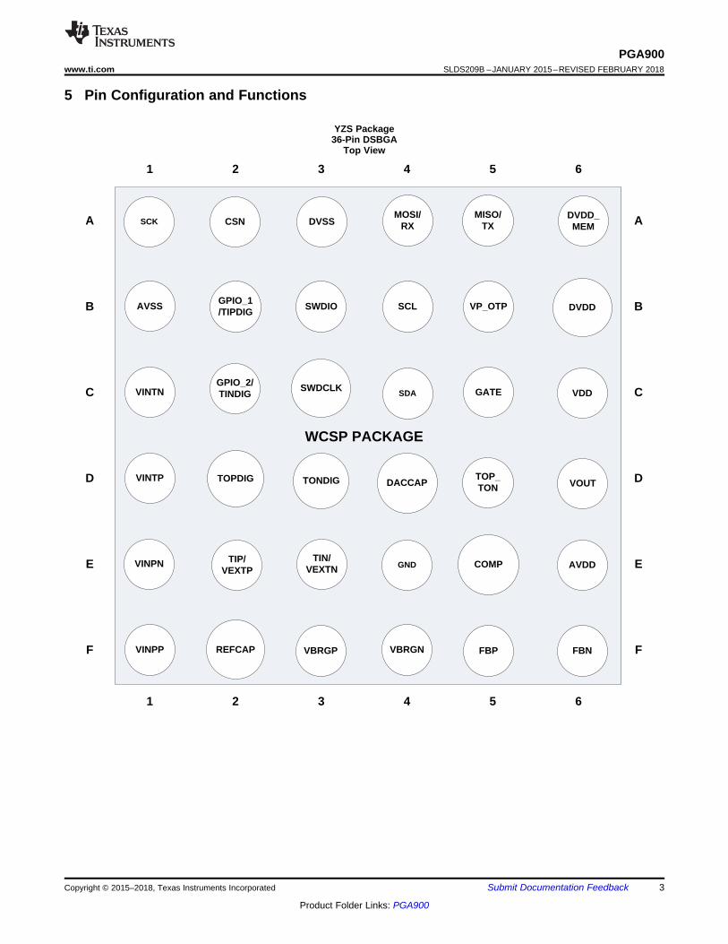
5 Pin Configuration and Functions
YZS Package36-Pin DSBGA
Top View

VP_OTP
DVDD_MEM
DVDD
VDD
AVDD
DACCAP
TOP_TON
GATE
VOUT
GPIO1/TIPDIG
GPIO2/TINDIG
TONDIG
AVSS
TIP/VEXTP
TIN/VEXTN
VINTN
TOPDIG
VINTP
FB
N
FB
P
CO
MP
RE
FC
AP
GN
D
VB
RG
N
VB
RG
P
VIN
PP
VIN
PN
MIS
O_T
X
MO
SI_
RX
DV
SS
SW
DIO
SW
DC
LK
SC
L
SD
A
CS
N
SC
K
10 11 12 13 14 15
24
23
22
21
20
19
QFN-36
6
1
2
3
4
5
17 1816
27
26
25
9
7
8
36 35 34 33 32 31 29 2830
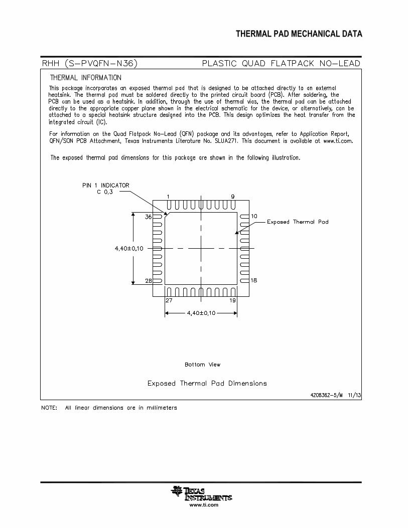
THERMAL PAD
4
PGA900SLDS209B –JANUARY 2015–REVISED FEBRUARY 2018 www.ti.com
Product Folder Links: PGA900
Submit Documentation Feedback Copyright © 2015–2018, Texas Instruments Incorporated
RHH Package36-Pin VQFN
Top View

5
PGA900www.ti.com SLDS209B –JANUARY 2015–REVISED FEBRUARY 2018
Product Folder Links: PGA900
Submit Documentation FeedbackCopyright © 2015–2018, Texas Instruments Incorporated
Pin FunctionsPIN
I/O DESCRIPTIONNAME DSBGA VQFNAVDD E6 9 O Analog voltageAVSS B1 23 — Analog groundCOMP E5 13 I Output compensationCSN A2 29 I SPI chip selectDACCAP D4 6 O DAC capacitorDVDD B6 3 O DVDD regulator outputDVDD_MEM A6 2 I Power supply for EEPROM and OTPDVSS A3 32 — Digital groundFBN F6 11 I Feedback NFBP F5 12 I Feedback PGATE C5 4 O N-channel depletion MOSFET driveGND E4 10 — GroundGPIO_1/TIPDIG B2 27 I/O General-purpose I/O 1 or digital test in P
GPIO_2/TINDIG C2 26 I/O General-purpose I/O 2 or digital test in N
MISO/TX A5 35 O SPI slave data out or UART TxMOSI/RX A4 34 I SPI slave data in or UART RxREFCAP F2 16 O ADC reference capacitorSCK A1 28 I SPI clockSCL B4 36 I I2C clockSDA C4 33 I/O I2C dataSWDCLK C3 30 I Serial wire debug clockSWDIO B3 31 I/O Serial wire debug I/OVBRGN F4 14 O Bridge drive NVBRGP F3 15 O Bridge drive PVDD C6 5 I Input power supplyVINTN C1 22 I External temperature sensor N inputVINTP D1 21 I External temperature sensor P inputVINPN E1 17 I Resistive sensor N inputVINPP F1 18 I Resistive sensor P inputVOUT D6 8 O DAC gain outputVP_OTP B5 1 I OTP programming voltageTONDIG D3 25 O Digital test output NTIN/VEXTN E3 20 I Analog test N in or V external N for T signal pathTIP/VEXTP E2 19 I Analog test P in or V external P for T signal pathTOP_TON D5 7 O Analog testout P or analog testout NTOPDIG D2 24 O Digital test output P

6
PGA900SLDS209B –JANUARY 2015–REVISED FEBRUARY 2018 www.ti.com
Product Folder Links: PGA900
Submit Documentation Feedback Copyright © 2015–2018, Texas Instruments Incorporated
(1) Stresses beyond those listed under Absolute Maximum Ratings may cause permanent damage to the device. These are stress ratingsonly, which do not imply functional operation of the device at these or any other conditions beyond those indicated under RecommendedOperating Conditions. Exposure to absolute-maximum-rated conditions for extended periods may affect device reliability.
6 Specifications
6.1 Absolute Maximum Ratingssee (1)
MIN MAX UNIT
Voltage
VDD –28 33
V
GATE –0.3 33At VP_OTP –0.3 8At sensor input and drive pins –0.3 2At any I/O pin –0.3 3.6At FBP pin –2 VDD + 0.3
IDD Short on VOUT supply current 25 mATJmax Maximum junction temperature 155 °CTlead Lead temperature (soldering, 10 s) 260 °CTstg Storage temperature –40 150 °C
6.2 ESD RatingsVALUE UNIT
V(ESD)Electrostaticdischarge
Human body model (HBM) – EIA/JESD22-A114 ±2000V
Field induced charge device model (CDM) – JESD22-C101 ±500
(1) Programming EEPROM results in additional 6 mA of current on VDD pin.
6.3 Recommended Operating Conditionsover operating free-air temperature range at VDD = 5 V (unless otherwise noted)
MIN NOM MAX UNITVDD Power supply voltage 3.3 30 V
Slew rate VDD = 0 to 30 V 0.5 V/µs
IDD Power supply current – normal operation No load on VBRG, no load on DAC, ƒ= 1 MHz 2.6 mA
IDDPower supply current – EEPROMprogramming
While EEPROM is beingprogrammed, no load on VBRG, noload on DAC
9 (1) mA
VP_OTP OTP programming voltage 7.2 7.6 7.8 VOTP programming voltage slew rate 1 V/µs
I_VP_OTP OTP programming current During OTP programming 5 mAtprog_OTP OTP programming timing per byte 120 200 µsTA Operating ambient temperature –40 150 °C
Programming temperature OTP or EEPROM –40 140 °CStart-up time (including analog anddigital) VDD ramp rate 0.5 V/µs 1 ms
Capacitor on VDD pin 10 nF

Tim
e to
Fai
l (H
r)
Continuous TJ (°C)
R2 = 0.999607233191242
90°C 7.7e+006 Hrs(8.8e+002 years)
100°C 2.2e+006 Hrs(2.5e+002 years)
110°C 6.8e+005 Hrs(77 years)
120°C 2.2e+005 Hrs(25 years)
130°C 7.6e+004 Hrs(8.6 years)
140°C 2.7e+004 Hrs(3.1 years)
80°C 2.9e+007 Hrs(3.3e+003 years)
1e+008
1e+007
1e+006
100000
10000
100080 90 100 110 120 130 140 150
7
PGA900www.ti.com SLDS209B –JANUARY 2015–REVISED FEBRUARY 2018
Product Folder Links: PGA900
Submit Documentation FeedbackCopyright © 2015–2018, Texas Instruments Incorporated
(1) For more information about traditional and new thermal metrics, see the Semiconductor and IC Package Thermal Metrics applicationreport.
6.4 Thermal Information
THERMAL METRIC (1)PGA900
UNITRHH (VQFN) YZS (DSBGA)36 PINS 36 PINS
RθJA Junction-to-ambient thermal resistance 30.6 49.4 °C/WRθJC(top) Junction-to-case (top) thermal resistance 16.4 0.1 °C/WRθJB Junction-to-board thermal resistance 5.4 10 °C/WψJT Junction-to-top characterization parameter 0.2 0.1 °C/WψJB Junction-to-board characterization parameter 5.4 10.1 °C/WRθJC(bot) Junction-to-case (bottom) thermal resistance 0.7 N/A °C/W
Figure 1. Estimated QFN Wirebond Life is 10392 hours (1.2 years)

69DOXH DW 7(03 ± 9DOXH DW &TEMP DRIFT 10
Value at 25 C TEMPq
uq u '
8
PGA900SLDS209B –JANUARY 2015–REVISED FEBRUARY 2018 www.ti.com
Product Folder Links: PGA900
Submit Documentation Feedback Copyright © 2015–2018, Texas Instruments Incorporated
(1) When Gate Drive is not being used, the GATE pin must be connected to GND and gate control must be disabled by settingGATE_CTRL_SD bit in ALPWR register to 1.
(2) When Gate Drive is used, a capacitor of up to 1 nF is recommended to be connected to the GATE pin. The gate threshold voltage forthe external depletion NMOS must be less than –1.5 V.
6.5 Electrical Characteristics—Gate Driveover operating free-air temperature range at VDD = 5 V (unless otherwise noted)
PARAMETER TEST CONDITIONS MIN TYP MAX UNITVDD voltage when using GATEcontrol (1) (2)
VDD = 5 V 3.5 V
PSRR while in regulation 87 dB
(1) Specified by design
6.6 Reverse Voltage Protectionover operating free-air temperature range at VDD = 5 V (unless otherwise noted)
PARAMETER TEST CONDITIONS MIN TYP MAX UNITReverse voltage –28 VVoltage drop across reverse voltageprotection element 20 mV
RDSon of reverse voltage protectionelement (1) VDD = 5 V 1.67 6.66 Ω
6.7 Regulatorsover operating free-air temperature range at VDD = 5 V (unless otherwise noted)
PARAMETER TEST CONDITIONS MIN TYP MAX UNITVAVDD AVDD voltage CAVDD = 100 nF 3 VVAVDD_POR AVDD voltage – digital POR 2.7 V
AVDD voltage – digital PORHysteresis 0.1 V
IAVDD External load on AVDD pin 4 mAVDVDD DVDD voltage – operating CDVDD = 100 nF 1.8 VVDVDD_POR DVDD voltage – digital POR 1.5 V
DVDD voltage – digital PORhysteresis 0.1 V
(1)
6.8 Internal Referenceover operating free-air temperature range at VDD = 5 V (unless otherwise noted)
PARAMETER MIN TYP MAX UNITInaccurate reference voltage 1.2 VAccurate reference voltage 2.5 VAccurate reference initial error –0.1% 0.1%Accurate reference voltage TC (1) –10 ±4.5 10 ppm/°CCapacitor value on REFCAP pin 10 1000 nF
6.9 Internal Oscillatorover operating free-air temperature range at VDD = 5 V (unless otherwise noted)
PARAMETER TEST CONDITIONS MIN TYP MAX UNITInternal oscillator frequency TA = 25°C 4 MHzInternal oscillator frequency variation Across operating temperature ±1%

2.5V
2.0V
1.25V
2.5VVBRGP
VINPP
VINPN
AVDDRegulator
3V Reverse Protection
2.5V Reference
2.5V
PGA ADC
VDD2.5VRefBuf
REFCAP
DAC
VBRGBuf
MUX
VOUT
DACCAP
100nF
3.3nF
40K DAC GAIN
vddp
A
B
C
E
R R
1.25V
AVDD
100nF
DVDDRegulator
DVDD
100nF
1.8V
RatiometricAbsolute R1
R1
ITEMPBuf
VINTP
69DOXH DW 7(03 ± 9DOXH DW &TEMP DRIFT 10
Value at 25 C TEMPq
uq u '
9
PGA900www.ti.com SLDS209B –JANUARY 2015–REVISED FEBRUARY 2018
Product Folder Links: PGA900
Submit Documentation FeedbackCopyright © 2015–2018, Texas Instruments Incorporated
(1)
6.10 Bridge Sensor Supplyover operating free-air temperature range at VDD = 5 V (unless otherwise noted)
PARAMETER TEST CONDITIONS MIN TYP MAX UNITVBRG SUPPLY FOR RESISTIVE BRIDGE SENSORS
VBRGP-VBRGN
Bridge supply voltage
Bridge supply control bit = 0b00, noload 2.5
VBridge supply control bit = 0b01, noload 2
Bridge supply control bit = 0b10, noload 1.25
Bridge supply voltage temperaturevariation (1)
Across temperature for 2.5 V bridgeoutput at no load 6.5 20
ppm/°CAcross temperature for 2 V bridgeoutput at no load 7.5
Across temperature for 1.25 V bridgeoutput at no load 15.5
IBRG Current supply to the bridge 1.5 mACBRG Capacitive load RBRG = 20 kΩ 2 nF
Figure 2. Bridge Supply and P ADC Reference are Ratiometric

69DOXH DW 7(03 ± 9DOXH DW &TEMP DRIFT 10
Value at 25 C TEMPq
uq u '
10
PGA900SLDS209B –JANUARY 2015–REVISED FEBRUARY 2018 www.ti.com
Product Folder Links: PGA900
Submit Documentation Feedback Copyright © 2015–2018, Texas Instruments Incorporated
(1)
6.11 Temperature Sensor Supplyover operating free-air temperature range at VDD = 5 V (unless otherwise noted)
PARAMETER TEST CONDITIONS MIN TYP MAX UNITITEMP SUPPLY FOR TEMPERATURE SENSOR
ITEMP Current supply to temperature sensor
Control bit = 0b000 25
µAControl bit = 0b001 50Control bit = 0b010 100Control bit = 0b011 500Control bit = 0b1xx off
ITEMP Current drift over temperature (1)
Control bit = 0b000 37
ppm/°CControl bit = 0b001 35Control bit = 0b010 42Control bit = 0b011 35
CTEMP Capacitive load 100 nFOutput impedance 15 MΩ
(1) For higher accuracy, each device must be calibrated using a two point method at 25°C and 125°C. Temperature can be calculated usingthe following formula, Output code = Offset + Gain × Temperature
6.12 Internal Temperature Sensorover operating free-air temperature range at VDD = 5 V (unless otherwise noted) (1)
PARAMETER TEST CONDITIONS MIN TYP MAX UNITTemperature range –40 150 °CGain 24-bit ADC 6632.1 LSB/°COffset 1710281.3 LSB
Total error without trim Using gain and offset valuesmentioned in this table ±6 °C

11
PGA900www.ti.com SLDS209B –JANUARY 2015–REVISED FEBRUARY 2018
Product Folder Links: PGA900
Submit Documentation FeedbackCopyright © 2015–2018, Texas Instruments Incorporated
(1) Specified by design
6.13 P Gain (Chopper Stabilized)over operating free-air temperature range at VDD = 5 V (unless otherwise noted)
PARAMETER TEST CONDITIONS MIN TYP MAX UNIT
Gain steps (5 bits)
00000, at DC 5
V/V
00001 5.4800010 5.9700011 6.5600100 7.0200101 8.0000110 9.0900111 10.0001000 10.5301001 11.1101010 12.5001011 13.3301100 14.2901101 16.0001110 17.3901111 18.1810000 19.0510001 20.0010010 22.2210011 2510100 30.7710101 36.3610110 40.0010111 44.4411000 5011001 57.1411010 66.6711011 8011100 10011101 133.3311110 20011111 400
Gain bandwidth product (1) 10 MHz
Input-referred noise density
ƒ = 0.1 Hz to 2 kHzTotal input-referred noise includinggain noise, ADC reference noise,ADC thermal noise, and ADCquantization noise at gain = 400V/V, sampling rate = 128 µs, acrosstemperature
15 nV/√Hz
Input offset voltage 10 µVInput offset voltage temperaturedrift 0.06 µV/°C
Gain temperature drift (1) Gain = 400 V/V –0.24 ppm/°CGain nonlinearity (1) Gain = 400 V/V 0.16 m%FSO
Total unadjusted error Includes offset error, gain error andINL across temperature 0.04 0.195 %FSO
Input bias current 5 nA
615 ± G%ENOB
6.02
12
PGA900SLDS209B –JANUARY 2015–REVISED FEBRUARY 2018 www.ti.com
Product Folder Links: PGA900
Submit Documentation Feedback Copyright © 2015–2018, Texas Instruments Incorporated
P Gain (Chopper Stabilized) (continued)over operating free-air temperature range at VDD = 5 V (unless otherwise noted)
PARAMETER TEST CONDITIONS MIN TYP MAX UNIT
(2) Common Mode at P Gain Input and Output has two constraints:(a) The single-ended voltage of positive/negative pin at the P Gain input must be between 0.3 and 1.8 V.(b) The single-ended voltage of positive/negative pin at the P Gain output must be between 0.1 and 2 V.
Frequency response (1) Gain = 400 V/V, <1 kHz ±0.1 %V/V
Common-mode voltage range
Dependson
selectedgain,
bridgesupply and
sensorspan (2)
V
Common-mode rejection ratio FCM= 50 Hz at Gain = 5 V/V 110 dBInput impedance 10 MΩ
(1)
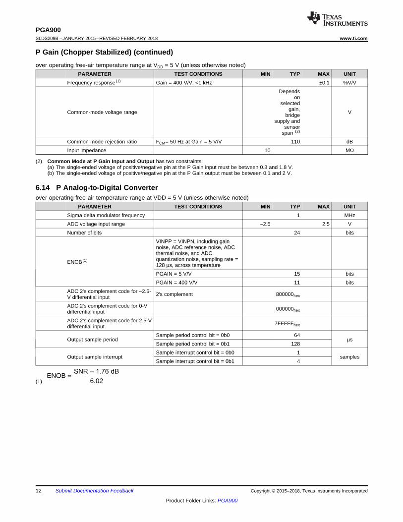
6.14 P Analog-to-Digital Converterover operating free-air temperature range at VDD = 5 V (unless otherwise noted)
PARAMETER TEST CONDITIONS MIN TYP MAX UNITSigma delta modulator frequency 1 MHzADC voltage input range –2.5 2.5 VNumber of bits 24 bits
ENOB (1)
VINPP = VINPN, including gainnoise, ADC reference noise, ADCthermal noise, and ADCquantization noise, sampling rate =128 µs, across temperaturePGAIN = 5 V/V 15 bitsPGAIN = 400 V/V 11 bits
ADC 2's complement code for –2.5-V differential input 2's complement 800000hex
ADC 2's complement code for 0-Vdifferential input 000000hex
ADC 2's complement code for 2.5-Vdifferential input 7FFFFFhex
Output sample periodSample period control bit = 0b0 64
µsSample period control bit = 0b1 128
Output sample interruptSample interrupt control bit = 0b0 1
samplesSample interrupt control bit = 0b1 4

13
PGA900www.ti.com SLDS209B –JANUARY 2015–REVISED FEBRUARY 2018
Product Folder Links: PGA900
Submit Documentation FeedbackCopyright © 2015–2018, Texas Instruments Incorporated
(1) Specified by design(2) Common Mode at T Gain Input and Output has two constraints:
(a) The single-ended voltage of positive/negative pin at the T gain input must be between 5 mV and 1.8 V.(b) The single-ended voltage of positive/negative pin at the T gain output must be between 0.1 and 2 V.
6.15 T Gain (Chopper Stabilized)over operating free-air temperature range at VDD = 5 V (unless otherwise noted)
PARAMETER TEST CONDITIONS MIN TYP MAX UNIT
Gain steps (2 bits)
Gain control bits = 0b00 at DC 1.33
V/VGain control bits = 0b01 2.00Gain control bits = 0b10 5.00Gain control bits = 0b11 20.00
Gain bandwidth product (1) 350 kHz
Input-referred noise density
ƒ = 0.1 Hz to 2 kHzTotal Input-referred noise includinggain noise, ADC reference noise,ADC thermal noise, and ADCquantization noise at gain = 5 V/V,sampling rate = 128 µs, acrosstemperature
110 nV/√Hz
Input offset voltage 95 µVInput offset voltage temperature drift 0.4 µV/°CGain temperature drift (1) Gain = 1.33 V/V 0.12 ppm/°CGain nonlinearity (1) Gain = 5 V/V 6.6 m%FSO
Total unadjusted error Includes offset error, gain error andINL across temperature 0.04 0.195 %FSO
Input bias current 5 nAFrequency response (1) Gain = 20 V/V, <100 Hz 0.335 %V/V
Common-mode voltage range
Dependson
selectedgain and
currentsupply (2)
Common-mode rejection ratio FCM = 50 Hz at Gain = 5 V/V 110 dBInput impedance 1 MΩ
615 ± G%ENOB
6.02
14
PGA900SLDS209B –JANUARY 2015–REVISED FEBRUARY 2018 www.ti.com
Product Folder Links: PGA900
Submit Documentation Feedback Copyright © 2015–2018, Texas Instruments Incorporated
(1)
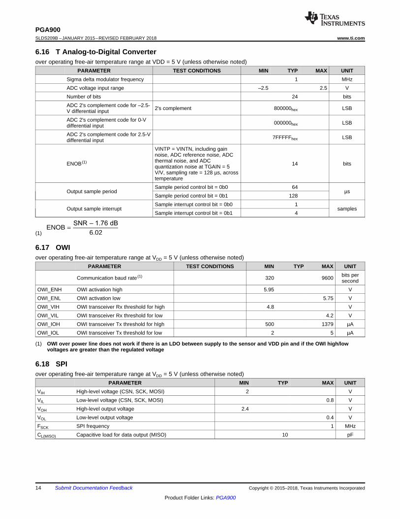
6.16 T Analog-to-Digital Converterover operating free-air temperature range at VDD = 5 V (unless otherwise noted)
PARAMETER TEST CONDITIONS MIN TYP MAX UNITSigma delta modulator frequency 1 MHzADC voltage input range –2.5 2.5 VNumber of bits 24 bitsADC 2's complement code for –2.5-V differential input 2's complement 800000hex LSB
ADC 2's complement code for 0-Vdifferential input 000000hex LSB
ADC 2's complement code for 2.5-Vdifferential input 7FFFFFhex LSB
ENOB (1)
VINTP = VINTN, including gainnoise, ADC reference noise, ADCthermal noise, and ADCquantization noise at TGAIN = 5V/V, sampling rate = 128 µs, acrosstemperature
14 bits
Output sample periodSample period control bit = 0b0 64
µsSample period control bit = 0b1 128
Output sample interruptSample interrupt control bit = 0b0 1
samplesSample interrupt control bit = 0b1 4
(1) OWI over power line does not work if there is an LDO between supply to the sensor and VDD pin and if the OWI high/lowvoltages are greater than the regulated voltage
6.17 OWIover operating free-air temperature range at VDD = 5 V (unless otherwise noted)
PARAMETER TEST CONDITIONS MIN TYP MAX UNIT
Communication baud rate (1) 320 9600 bits persecond
OWI_ENH OWI activation high 5.95 VOWI_ENL OWI activation low 5.75 VOWI_VIH OWI transceiver Rx threshold for high 4.8 VOWI_VIL OWI transceiver Rx threshold for low 4.2 VOWI_IOH OWI transceiver Tx threshold for hIgh 500 1379 µAOWI_IOL OWI transceiver Tx threshold for low 2 5 µA
6.18 SPIover operating free-air temperature range at VDD = 5 V (unless otherwise noted)
PARAMETER MIN TYP MAX UNITVIH High-level voltage (CSN, SCK, MOSI) 2 VVIL Low-level voltage (CSN, SCK, MOSI) 0.8 VVOH High-level output voltage 2.4 VVOL Low-level output voltage 0.4 VFSCK SPI frequency 1 MHzCL(MISO) Capacitive load for data output (MISO) 10 pF

15
PGA900www.ti.com SLDS209B –JANUARY 2015–REVISED FEBRUARY 2018
Product Folder Links: PGA900
Submit Documentation FeedbackCopyright © 2015–2018, Texas Instruments Incorporated
6.19 I2C Interfaceover operating free-air temperature range at VDD = 5 V (unless otherwise noted)
PARAMETER TEST CONDITIONS MIN TYP MAX UNIT
VIH High-level input voltage 0.7 ×AVDD V
VIL Low-level input voltage 0.3 ×AVDD V
VOL Low-level output voltage IOL = 3 mA, I2C RATE configurationbit = 0 0.4 V
VOL Low-level output voltage IOL = 20 mA, I2C RATE configurationbit = 1 0.4 V
ƒSCL SCL clock frequency 800 KBPS
6.20 PWM Outputover operating free-air temperature range at VDD = 5 V (unless otherwise noted)
PARAMETER TEST CONDITIONS MIN TYP MAX UNITPWM timer 4 MHzPWM timer bits 16 bits
6.21 DAC Outputover operating free-air temperature range at VDD = 5 V (unless otherwise noted)
PARAMETER TEST CONDITIONS MIN TYP MAX UNIT
DAC reference voltageReference bit = 1 1.25
VReference bit = 0 (ratiometric) 0.25 × Vddp
DAC resolution 14 bits
(1) Specified by design
6.22 DAC Gainover operating free-air temperature range at VDD = 5 V (unless otherwise noted)
PARAMETER TEST CONDITIONS MIN TYP MAX UNIT
Buffer gain (see Figure 3)
2X 2
V/V4X 46.67X 6.6710X 10
Current loop gain 1001 mA/mAGain bandwidth product (1) 1 MHz
Offset error Gain = 4X, ratiometric outputmeasured at VOUT ±13 mV
Gain error Gain = 4X, ratiometric outputmeasured at VOUT ±0.3 %FSR
Ratiometric error For ratiometric applications, acrosstemperature ±0.1 %FSO
Total unadjusted error
Current mode output3.5 %FSOIncludes offset error, gain error and
INL across temperatureVoltage mode output
0.15 %FSOIncludes offset error, gain error andINL across temperature

69DOXH DW 7(03 ± 9DOXH DW &TEMP DRIFT 10
Value at 25 C TEMPq
uq u '
16
PGA900SLDS209B –JANUARY 2015–REVISED FEBRUARY 2018 www.ti.com
Product Folder Links: PGA900
Submit Documentation Feedback Copyright © 2015–2018, Texas Instruments Incorporated
DAC Gain (continued)over operating free-air temperature range at VDD = 5 V (unless otherwise noted)
PARAMETER TEST CONDITIONS MIN TYP MAX UNIT
(2)
Ratiometric error due to change intemperature and load current forDAC Code = 8192d (Mid-Code).
Calculate ratiometric error at VDD =5 V and at DAC codes as follows:1. Apply DAC Code at 25°C and
0-mA load, and measurevoltage at VOUT
2. Change temperature between–40°C to 125°C, and measurevoltage at VOUT
3. Change load current between 0mA to 2.5 mA, and measurevoltage at VOUT
4. Ratiometric Error = ((VOUT atTEMPERATURE at LOAD) –(VOUT at 25°C at 0 mA))
3 mV
DAC gain noise
ƒ = 10 Hz to 1 kHz, VDD = 4.5 V,ratiometric mode, gain = 4 V/V, nocapacitors for COMP or DACCAPpins, 25°C
10 uVpp
Settling time (first order response) (1)DAC code 0000h to 1FFFh step.Output is 90% of full scale. RLOAD =5 kΩ, CLOAD = 500 pF
7 µs
Zero code voltage (Gain = 4X) DAC code = 0000h, IDAC = –2.5 mA 20 mV
Full code voltage (Gain = 4X) Output when DAC code is 1FFFh,IDAC = 2.5 mA 4.8 V
Absolute mode voltage half codetemperature drift, IDAC = 2.5 mA (2)
Gain = 2X 6 25
ppm/°CGain = 4X 6 26.5Gain = 6.67X 6 28.5Gain = 10X 7 30
Ratiometric mode voltage half codetemperature drift, Gain = 4X (2)
No load 21.5 38ppm/°C
IDAC = 1.25 mA 30.5 49.5
Output current DAC code = 1FFFh , DAC code =0000h ±2.5 mA
Short-circuit source current DAC code = 0000h 27 mAShort-circuit sink current DAC code = 1FFFh 27 mA
Max capacitanceWithout compensation 100 pFWith compensation 100 nF

+
VDAC
VOUT
Vddp
DACCAP
40K
-
FBP
FBN
COMP
40
75K 2V/V
4V/V
6.67V/V
S5
40K
10V/V
Open
37.5K
15K
7.5K
15K
S4
S0,S1,S2,S3
S8
172K
302K S7
2.5V (From Accurate Reference or Vddp/2)
17
PGA900www.ti.com SLDS209B –JANUARY 2015–REVISED FEBRUARY 2018
Product Folder Links: PGA900
Submit Documentation FeedbackCopyright © 2015–2018, Texas Instruments Incorporated
Figure 3. PGA900 Output Buffer
18
PGA900SLDS209B –JANUARY 2015–REVISED FEBRUARY 2018 www.ti.com
Product Folder Links: PGA900
Submit Documentation Feedback Copyright © 2015–2018, Texas Instruments Incorporated
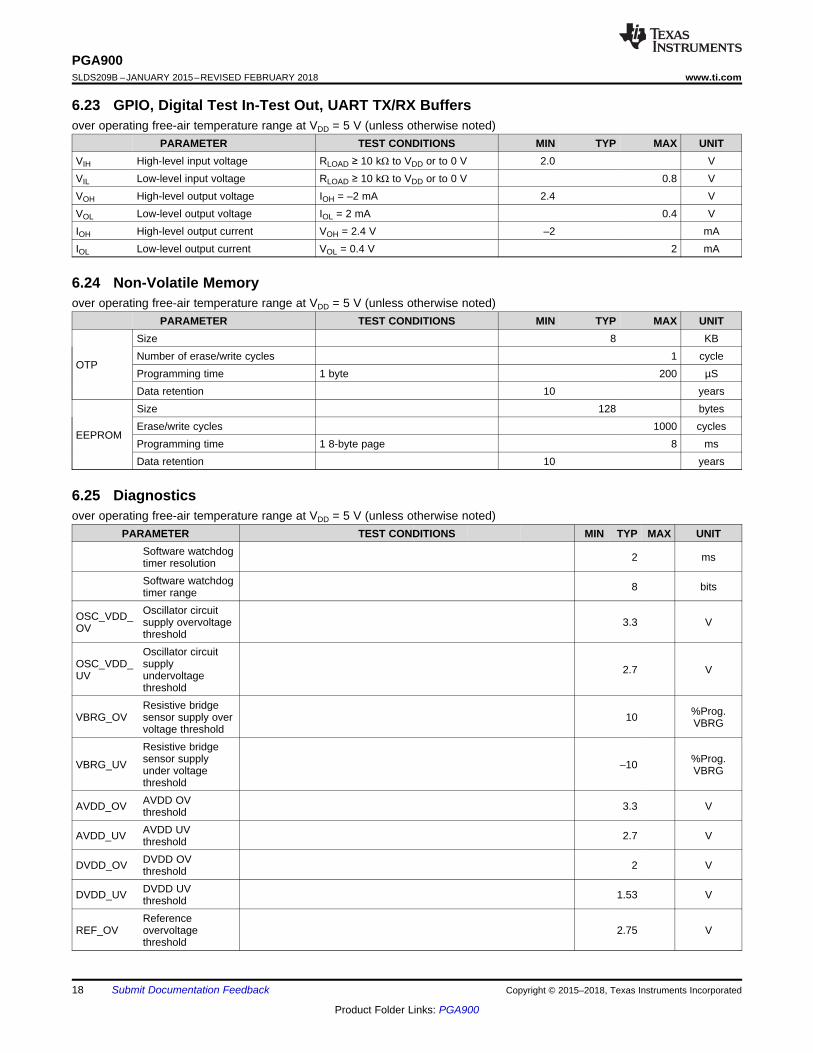
6.23 GPIO, Digital Test In-Test Out, UART TX/RX Buffersover operating free-air temperature range at VDD = 5 V (unless otherwise noted)
PARAMETER TEST CONDITIONS MIN TYP MAX UNITVIH High-level input voltage RLOAD ≥ 10 kΩ to VDD or to 0 V 2.0 VVIL Low-level input voltage RLOAD ≥ 10 kΩ to VDD or to 0 V 0.8 VVOH High-level output voltage IOH = –2 mA 2.4 VVOL Low-level output voltage IOL = 2 mA 0.4 VIOH High-level output current VOH = 2.4 V –2 mAIOL Low-level output current VOL = 0.4 V 2 mA
6.24 Non-Volatile Memoryover operating free-air temperature range at VDD = 5 V (unless otherwise noted)
PARAMETER TEST CONDITIONS MIN TYP MAX UNIT
OTP
Size 8 KBNumber of erase/write cycles 1 cycleProgramming time 1 byte 200 µSData retention 10 years
EEPROM
Size 128 bytesErase/write cycles 1000 cyclesProgramming time 1 8-byte page 8 msData retention 10 years
6.25 Diagnosticsover operating free-air temperature range at VDD = 5 V (unless otherwise noted)
PARAMETER TEST CONDITIONS MIN TYP MAX UNITSoftware watchdogtimer resolution 2 ms
Software watchdogtimer range 8 bits
OSC_VDD_OV
Oscillator circuitsupply overvoltagethreshold
3.3 V
OSC_VDD_UV
Oscillator circuitsupplyundervoltagethreshold
2.7 V
VBRG_OVResistive bridgesensor supply overvoltage threshold
10 %Prog.VBRG
VBRG_UV
Resistive bridgesensor supplyunder voltagethreshold
–10 %Prog.VBRG
AVDD_OV AVDD OVthreshold 3.3 V
AVDD_UV AVDD UVthreshold 2.7 V
DVDD_OV DVDD OVthreshold 2 V
DVDD_UV DVDD UVthreshold 1.53 V
REF_OVReferenceovervoltagethreshold
2.75 V

19
PGA900www.ti.com SLDS209B –JANUARY 2015–REVISED FEBRUARY 2018
Product Folder Links: PGA900
Submit Documentation FeedbackCopyright © 2015–2018, Texas Instruments Incorporated
Diagnostics (continued)over operating free-air temperature range at VDD = 5 V (unless otherwise noted)
PARAMETER TEST CONDITIONS MIN TYP MAX UNIT
REF_UVReferenceundervoltagethreshold
2.25 V
P_DIAG_PU
P gain inputdiagnosticspulldown resistorvalue
VINPP and VINPN each has pulldown resistor
1
MΩ234
VINP_OVP gain inputovervoltagethreshold value
VINPP and VINPN each hasthreshold comparator
FAULT_THRS[2]
FAULT_THRS[1]
FAULT_THRS[0]
% VBRDG
VBRDG = 2.5 V0 0 0 72.50 0 1 700 1 0 65
VBRDG = 2 V0 1 1 901 0 0 87.51 0 1 82.5
VBRDG = 1.25 V1 1 0 1001 1 1 95
VINP_UVP gain inputundervoltagethreshold value
VINPP and VINPN each hasthreshold comparator
FAULT_THRS[2]
FAULT_THRS[1]
FAULT_THRS[0]
% VBRDG
VBRDG = 2.5 V0 0 0 7.50 0 1 100 1 0 15
VBRDG = 2 V0 1 1 101 0 0 12.51 0 1 17.5
VBRDG = 1.25 V1 1 0 17.51 1 1 22.5
VINT_OV T gain inputovervoltage VINTP and VINTN 2.1 V
PGAIN_OV
Output overvoltage(single-ended)threshold for Pgain
2.25 V
PGAIN_UV
Outputundervoltage(single-ended)threshold for Pgain
0.15 V
TGAIN_OVOutput overvoltage(single-ended)threshold for T gain
2.25 V
TGAIN_UV
Outputundervoltage(single-ended)threshold for T gain
0.15 V
DAC_LB
DAC loop backvoltage gain 0.2 V/V
DAC loop backdriving capability 10 µA
HARNESS_FAULT1
Open wire leakagecurrent 1 - openVDD with pullup onVOUT1
2 µA
20
PGA900SLDS209B –JANUARY 2015–REVISED FEBRUARY 2018 www.ti.com
Product Folder Links: PGA900
Submit Documentation Feedback Copyright © 2015–2018, Texas Instruments Incorporated
Diagnostics (continued)over operating free-air temperature range at VDD = 5 V (unless otherwise noted)
PARAMETER TEST CONDITIONS MIN TYP MAX UNIT
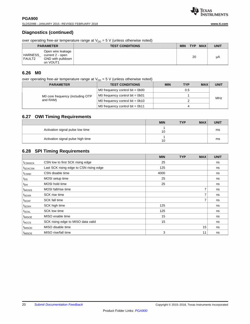
HARNESS_FAULT2
Open wire leakagecurrent 2 - openGND with pulldownon VOUT1
20 µA
6.26 M0over operating free-air temperature range at VDD = 5 V (unless otherwise noted)
PARAMETER TEST CONDITIONS MIN TYP MAX UNIT
M0 core frequency (including OTPand RAM)
M0 frequency control bit = 0b00 0.5
MHzM0 frequency control bit = 0b01 1M0 frequency control bit = 0b10 2M0 frequency control bit = 0b11 4
6.27 OWI Timing RequirementsMIN TYP MAX UNIT
Activation signal pulse low time 110 ms
Activation signal pulse high time 110 ms
6.28 SPI Timing RequirementsMIN TYP MAX UNIT
tCSNSCK CSN low to first SCK rising edge 25 nstSCKCSN Last SCK rising edge to CSN rising edge 125 nstCSND CSN disable time 4000 nstDS MOSI setup time 25 nstDH MOSI hold time 25 nstMOSIS MOSI fall/rise time 7 nstSCKR SCK rise time 7 nstSCKF SCK fall time 7 nstSCKH SCK high time 125 nstSCKL SCK low time 125 nstMISOE MISO enable time 15 nstACCS SCK rising edge to MISO data valid 15 nstMISOD MISO disable time 15 nstMISOS MISO rise/fall time 3 11 ns

TCSNSCK TSCKCSN
TCSND
TDS TDH
MSB LSB
TSCKRTSCKF
TSCKL
TSCKH
MSB LSB
TACCS
TMISOE
TMISOD
TMISOS
TMOSIS
CSN
SCK
MOSI
MISO
21
PGA900www.ti.com SLDS209B –JANUARY 2015–REVISED FEBRUARY 2018
Product Folder Links: PGA900
Submit Documentation FeedbackCopyright © 2015–2018, Texas Instruments Incorporated
Figure 4. SPI Timing

tSTASU
tSTAHD
tLOW
tHIGH
tRISEtFALL
tDATSU
tDATHD tSTOSU
22
PGA900SLDS209B –JANUARY 2015–REVISED FEBRUARY 2018 www.ti.com
Product Folder Links: PGA900
Submit Documentation Feedback Copyright © 2015–2018, Texas Instruments Incorporated
6.29 I2C Interface Timing RequirementsMIN TYP MAX UNIT
tSTASU START condition set-up time 500 nstSTAHD START condition hold time 500 nstLOW SCL low time 1.25 µstHIGH SCL high time 1.25 µstRISE SCL and SDA rise time 120 nstFALL SCL and SDA fall time 120 nstDATSU Data setup time 500 nstDATHD Data hold time 500 nstSTOSU STOP condition set-up time 500 ns
Figure 5. I2C Timing

Temperature (°C)
Tem
p P
ath
INL
Err
or (
%F
S)
-40 -20 0 20 40 60 80 100 120 140 1600.01
0.02
0.03
0.04
0.05
0.06
0.07
0.08
0.09
0.1
0.11
D006
1.33 V/V20 V/V
DAC Code (decimal)
%F
SO
0 2000 4000 6000 8000 10000 12000 14000 16000-0.12
-0.1
-0.08
-0.06
-0.04
-0.02
0
D008
-40 °C25 °C125 °C150 °C
Temperature (°C)
Pre
ssur
e P
ath
INL
Err
or (
%F
S)
-40 -20 0 20 40 60 80 100 120 140 1600
0.01
0.02
0.03
0.04
0.05
0.06
0.07
0.08
0.09
0.1
D004
5 V/V100 V/V200 V/V400 V/V
Temperature (°C)
Tem
p P
ath
INL
Err
or (
%F
S)
-40 -20 0 20 40 60 80 100 120 140 1600.005
0.015
0.025
0.035
0.045
0.055
0.065
0.075
0.085
D005
1.33 V/V5 V/V20 V/V
Temperature (°C)
Osc
illat
or F
requ
ency
(M
Hz)
-40 -20 0 20 40 60 80 100 120 140 1603.95
3.9553.96
3.9653.97
3.9753.98
3.9853.99
3.9954
4.0054.01
4.0154.02
D002Temperature (°C)
Tem
p S
enso
r C
ode
(dec
)
-40 -20 0 20 40 60 80 100 120 140 1601400000
1600000
1800000
2000000
2200000
2400000
2600000
2800000
D003
23
PGA900www.ti.com SLDS209B –JANUARY 2015–REVISED FEBRUARY 2018
Product Folder Links: PGA900
Submit Documentation FeedbackCopyright © 2015–2018, Texas Instruments Incorporated
6.30 Typical Characteristics
Figure 6. Oscillator Frequency vs Temperature Figure 7. Temperature Sensor Code vs Temperature
Figure 8. Pressure Path INL Error (Differential) vsTemperature
Figure 9. Temperature Path INL Error (Differential) vsTemperature
Figure 10. Temperature Path INL Error (Single-Ended) vsTemperature
Figure 11. Voltage Mode DAC Output Across Temperature

VDD (V)
IDD
(m
A)
3 6 9 12 15 18 21 24 27 302.00
2.05
2.10
2.15
2.20
2.25
2.30
2.35
2.40
2.45
2.50
D009
-40 °C25 °C125 °C150 °C
M0 Frequency (MHz)
IDD
(m
A)
0.5 1.0 1.5 2.0 2.5 3.0 3.5 4.01.8
2.0
2.2
2.4
2.6
2.8
3.0
D010
-40 °C25 °C125 °C150 °C
DAC Code (decimal)
%F
SO
0 2000 4000 6000 8000 10000 12000 14000 16000-7
-6.5
-6
-5.5
-5
-4.5
-4
-3.5
-3
-2.5
-2
-1.5
-1
-0.5
D011
-40 °C25 °C125 °C150 °C
DAC Code (decimal)
%F
SO
10912 11112 11312 11512 11712 11912-5.3
-5.2
-5.1
-5
-4.9
-4.8
-4.7
-4.6
D012
-40 °C25 °C125 °C150 °C
24
PGA900SLDS209B –JANUARY 2015–REVISED FEBRUARY 2018 www.ti.com
Product Folder Links: PGA900
Submit Documentation Feedback Copyright © 2015–2018, Texas Instruments Incorporated
Typical Characteristics (continued)
Figure 12. Current Mode DAC Output Across Temperature
Zoomed in section of Figure 12 to indicate drift across temperature
Figure 13. Current Mode DAC Output Across Temperature
M0 Frequency = 1 MHz
Figure 14. IDD vs VDD Across Temperature
VDD = 5 V, code through OTP
Figure 15. IDD vs Frequency Across Temperature
25
PGA900www.ti.com SLDS209B –JANUARY 2015–REVISED FEBRUARY 2018
Product Folder Links: PGA900
Submit Documentation FeedbackCopyright © 2015–2018, Texas Instruments Incorporated
7 Detailed Description
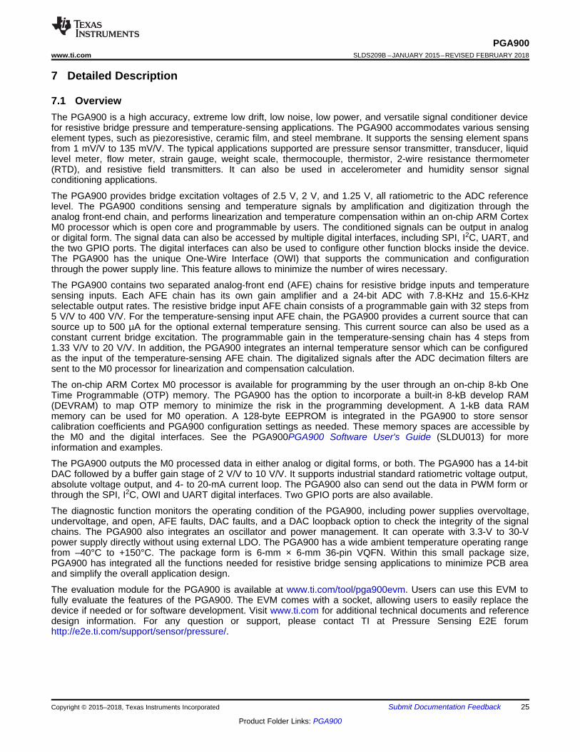
7.1 OverviewThe PGA900 is a high accuracy, extreme low drift, low noise, low power, and versatile signal conditioner devicefor resistive bridge pressure and temperature-sensing applications. The PGA900 accommodates various sensingelement types, such as piezoresistive, ceramic film, and steel membrane. It supports the sensing element spansfrom 1 mV/V to 135 mV/V. The typical applications supported are pressure sensor transmitter, transducer, liquidlevel meter, flow meter, strain gauge, weight scale, thermocouple, thermistor, 2-wire resistance thermometer(RTD), and resistive field transmitters. It can also be used in accelerometer and humidity sensor signalconditioning applications.
The PGA900 provides bridge excitation voltages of 2.5 V, 2 V, and 1.25 V, all ratiometric to the ADC referencelevel. The PGA900 conditions sensing and temperature signals by amplification and digitization through theanalog front-end chain, and performs linearization and temperature compensation within an on-chip ARM CortexM0 processor which is open core and programmable by users. The conditioned signals can be output in analogor digital form. The signal data can also be accessed by multiple digital interfaces, including SPI, I2C, UART, andthe two GPIO ports. The digital interfaces can also be used to configure other function blocks inside the device.The PGA900 has the unique One-Wire Interface (OWI) that supports the communication and configurationthrough the power supply line. This feature allows to minimize the number of wires necessary.
The PGA900 contains two separated analog-front end (AFE) chains for resistive bridge inputs and temperaturesensing inputs. Each AFE chain has its own gain amplifier and a 24-bit ADC with 7.8-KHz and 15.6-KHzselectable output rates. The resistive bridge input AFE chain consists of a programmable gain with 32 steps from5 V/V to 400 V/V. For the temperature-sensing input AFE chain, the PGA900 provides a current source that cansource up to 500 µA for the optional external temperature sensing. This current source can also be used as aconstant current bridge excitation. The programmable gain in the temperature-sensing chain has 4 steps from1.33 V/V to 20 V/V. In addition, the PGA900 integrates an internal temperature sensor which can be configuredas the input of the temperature-sensing AFE chain. The digitalized signals after the ADC decimation filters aresent to the M0 processor for linearization and compensation calculation.
The on-chip ARM Cortex M0 processor is available for programming by the user through an on-chip 8-kb OneTime Programmable (OTP) memory. The PGA900 has the option to incorporate a built-in 8-kB develop RAM(DEVRAM) to map OTP memory to minimize the risk in the programming development. A 1-kB data RAMmemory can be used for M0 operation. A 128-byte EEPROM is integrated in the PGA900 to store sensorcalibration coefficients and PGA900 configuration settings as needed. These memory spaces are accessible bythe M0 and the digital interfaces. See the PGA900PGA900 Software User's Guide (SLDU013) for moreinformation and examples.
The PGA900 outputs the M0 processed data in either analog or digital forms, or both. The PGA900 has a 14-bitDAC followed by a buffer gain stage of 2 V/V to 10 V/V. It supports industrial standard ratiometric voltage output,absolute voltage output, and 4- to 20-mA current loop. The PGA900 also can send out the data in PWM form orthrough the SPI, I2C, OWI and UART digital interfaces. Two GPIO ports are also available.
The diagnostic function monitors the operating condition of the PGA900, including power supplies overvoltage,undervoltage, and open, AFE faults, DAC faults, and a DAC loopback option to check the integrity of the signalchains. The PGA900 also integrates an oscillator and power management. It can operate with 3.3-V to 30-Vpower supply directly without using external LDO. The PGA900 has a wide ambient temperature operating rangefrom –40°C to +150°C. The package form is 6-mm × 6-mm 36-pin VQFN. Within this small package size,PGA900 has integrated all the functions needed for resistive bridge sensing applications to minimize PCB areaand simplify the overall application design.
The evaluation module for the PGA900 is available at www.ti.com/tool/pga900evm. Users can use this EVM tofully evaluate the features of the PGA900. The EVM comes with a socket, allowing users to easily replace thedevice if needed or for software development. Visit www.ti.com for additional technical documents and referencedesign information. For any question or support, please contact TI at Pressure Sensing E2E forumhttp://e2e.ti.com/support/sensor/pressure/.

LINEAR REGULATORS
BANDGAP + CURRENT
INTERNAL OSC
I_Osc
System Clock
CSN
SCK
TONDIG
GPIO_1/TIPDIG
GPIO_2/TINDIG
DIAGNOSTICS
SCL
SDA
VDD
ARM CORTEX M0
EEPROM(128 Bytes)
OTP(8KB)
RAM(1KB)
DAC GAIN(2 Bits)
FBP
CONTROL & STATUS
OWI DRIVER SPI DRIVER
³,2&´DRIVER
REVERSE VOLTAGE
PROTECTION
Vddp
VP_OTP
tx
rx
GND
REFCAP
AVDD
OWI
SPI
I2C
DAC
PWM
GPIO
GPIO/UART
DRIVER
AVDD
DVDD
FBN
TOP_TON
DVSS
AVSS
P SIGMA DELTA
MODULATOR
P DECIMATION FILTER
PADC
VINPP
VINPNMemoryP GAIN
(5 Bits)
Vddp
Vddp
+
-
ACCURATE REFERENCE(2.5V)
VOUT
T DECIMATION FILTER
TADC
Memory
Channel Select
MU
X
VINTN
VINTP
DACCAP
DE
BU
GG
ERSWDCLK
SWDIO
SWDIO
SWDCLK
T SIGMA DELTA
MODULATOR
T GAIN (2 Bits)
Internal Temperature
vtint
GATE DRIVEGATE
TOPDIG
UART
MISO/TX
MOSI/RXTIP/VEXTP
COMP
TIN/VEXTN
DVDD
DVDD_MEM
req
SENSOR VOLTAGE SUPPLY
VBRGP
BRIDGE DRIVE
VBRGN
DEVRAM(8KB)
INACCURATE REFERENCE(1.2V)
RE
FR
EF
REF
RE
F
AV
DD
AVDD
SPI DRIVER
26
PGA900SLDS209B –JANUARY 2015–REVISED FEBRUARY 2018 www.ti.com
Product Folder Links: PGA900
Submit Documentation Feedback Copyright © 2015–2018, Texas Instruments Incorporated
7.2 Functional Block Diagram

To rest of the IC VDD (3.5V)
GATE
VIN (>30V)
27
PGA900www.ti.com SLDS209B –JANUARY 2015–REVISED FEBRUARY 2018
Product Folder Links: PGA900
Submit Documentation FeedbackCopyright © 2015–2018, Texas Instruments Incorporated
7.3 Feature DescriptionThis section describes individual functional blocks.
7.3.1 Gate Drive for N-Channel Depletion NMOSThe PGA900 includes gate control for an external N-channel depletion MOSFET used as the pass element for aLDO. The gate threshold voltage for the MOSFET must be less than –1.5 V. When the device is used in thismode, VDD is regulated to 3.5 V by PGA900. A capacitor of 1 nF or less is recommended to be added to theGATE pin. Figure 16 shows a block diagram representation of the MOSFET gate drive.
If gate drive mode is not used, then the user must do the following:1. Connect GATE pin to ground.2. Disable gate control by setting GATE_CTRL_SD bit in ALPWR register to 1.
Figure 16. Gate Drive for N-Channel Depletion MOSFET
NOTEIf PGA900 is operated in gate drive mode, then VDD cannot be driven directly from anexternal voltage source.

VDD
10
MQ
VDDP
28
PGA900SLDS209B –JANUARY 2015–REVISED FEBRUARY 2018 www.ti.com
Product Folder Links: PGA900
Submit Documentation Feedback Copyright © 2015–2018, Texas Instruments Incorporated
Feature Description (continued)7.3.2 Reverse Voltage Protection BlockThe PGA900 includes reverse voltage protection block. This block protects the device from reverse-batteryconditions on the external power supply. Figure 17 shows a schematic of the reverse protection block.
Figure 17. Reverse Voltage Protection Block
7.3.3 Linear RegulatorsThe PGA900 has two main linear regulators: AVDD regulator and DVDD regulator. The AVDD regulator providesthe 3-V voltage source for internal analog circuitry while the DVDD regulator provides the 1.8-V regulated voltagefor the digital circuitry. The user needs to connect bypass capacitors of 100 nF each on the AVDD and DVDDpins of the device.
The power-on reset (POR) signal to the digital core are de-asserted when both AVDD and DVDD are inregulation. Figure 18 shows the block diagram representation of the digital POR signal generation and Figure 19shows the digital POR signal assertion/deassertion timing during VDD ramp up and ramp down. This timingshows that during power up, the digital core and the microprocessor remain in reset state until both AVDD andDVDD are at stable levels.

VAVDD_POR
VDVDD_POR
VDD
AVDD
DVDD
Digital POR
Microprocessor starts running Microprocessor stops running
time
Voltage
DVDD Regulator
AVDD Regulator
vddp DVDD
AVDD
Digital Core(Including M0 processor)
Digital_Power_Good
POR
VDVDD_POR
VAVDD_POR
Reset DVDD
DVSS
29
PGA900www.ti.com SLDS209B –JANUARY 2015–REVISED FEBRUARY 2018
Product Folder Links: PGA900
Submit Documentation FeedbackCopyright © 2015–2018, Texas Instruments Incorporated
Feature Description (continued)
Figure 18. Digital POR Signal Generation
Figure 19. Digital POR Signal Generation
7.3.4 Internal ReferencePGA900 has two internal references. The following sections describe each of these references.
7.3.4.1 Inaccurate ReferenceThe inaccurate reference is an inaccurate reference used in the gate drive circuit as well as diagnosticthresholds.
30
PGA900SLDS209B –JANUARY 2015–REVISED FEBRUARY 2018 www.ti.com
Product Folder Links: PGA900
Submit Documentation Feedback Copyright © 2015–2018, Texas Instruments Incorporated
Feature Description (continued)7.3.4.2 Accurate ReferenceThe accurate reference is used to generate reference voltage for P ADC, T ADC, and the DAC. TI recommendsplacing a 100-nF capacitor on REFCAP pin to bandwidth limit the reference noise.
The accurate reference buffer can be disabled by setting ADC_EN_VREF bit in ALPWR register to 0. This allowsthe user to connect an external single-ended reference voltage to REFCAP pin, and thus provide the referencevoltage to the ADCs and the DAC. Note that the default power-up state of ADC_EN_VREF is such that thereference buffer is disabled.
NOTEThe accurate reference is valid 50 µs after digital core starts running at power up.
7.3.5 Internal OscillatorThe device includes an internal 4-MHz oscillator. This oscillator provides the internal clock required for thevarious circuits in PGA900.
7.3.6 VBRGP/VBRGN Supply for Resistive BridgeThe sensor voltage supply block of the PGA900 supplies power to the resistive sense element. The sensorsupply in the PGA900 is configurable to 2.5-V, 2-V, and 1.2-V nominal output supply using the VBRDG_CTRLbits in BRDG_CTRL register to accommodate bridge sense elements with different resistance values. Thisnominal supply is ratiometric to the precise internal accurate reference.
The sensor drive includes a switch. This switch can be used to turn off power to the sensing element.
7.3.7 ITEMP Supply for Temperature SensorThe ITEMP block in PGA900 supplies programmable current to an external temperature sensor such as PTC.The temperature sensor current source is ratiometric to the accurate reference.
The value of the current can be programmed using the ITEMP_CTRL bits in TEMP_CTRL register.
VINPP VINPNVOCM
292',)) 3*$,1 9,133 ± 9,131
u
VINPP VINPNVICM
29,',)) 9,133 ± 9,131
T GAIN
VPTAT
VREF = 2.5 V
T ADC
31
PGA900www.ti.com SLDS209B –JANUARY 2015–REVISED FEBRUARY 2018
Product Folder Links: PGA900
Submit Documentation FeedbackCopyright © 2015–2018, Texas Instruments Incorporated
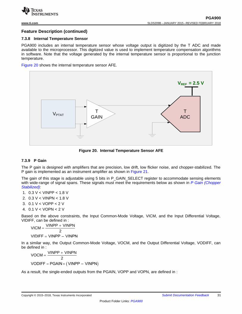
Feature Description (continued)7.3.8 Internal Temperature SensorPGA900 includes an internal temperature sensor whose voltage output is digitized by the T ADC and madeavailable to the microprocessor. This digitized value is used to implement temperature compensation algorithmsin software. Note that the voltage generated by the internal temperature sensor is proportional to the junctiontemperature.
Figure 20 shows the internal temperature sensor AFE.
Figure 20. Internal Temperature Sensor AFE
7.3.9 P GainThe P gain is designed with amplifiers that are precision, low drift, low flicker noise, and chopper-stabilized. TheP gain is implemented as an instrument amplifier as shown in Figure 21.
The gain of this stage is adjustable using 5 bits in P_GAIN_SELECT register to accommodate sensing elementswith wide-range of signal spans. These signals must meet the requirements below as shown in P Gain (ChopperStabilized):1. 0.3 V < VINPP < 1.8 V2. 0.3 V < VINPN < 1.8 V3. 0.1 V < VOPP < 2 V4. 0.1 V < VOPN < 2 V
Based on the above constraints, the Input Common-Mode Voltage, VICM, and the Input Differential Voltage,VIDIFF, can be defined in :
In a similar way, the Output Common-Mode Voltage, VOCM, and the Output Differential Voltage, VODIFF, canbe defined in :
As a result, the single-ended outputs from the PGAIN, VOPP and VOPN, are defined in :

VINPP
VINPN
+
+
-
-
To ADC
PGAIN_OPEN
VOPP
VOPN
ýþþ =÷üþþ + ÷üþü
Û+ þõï÷ü×
÷üþþF ÷üþü
Û
ýþü =÷üþþ + ÷üþü
ÛF þõï÷ü×
÷üþþF ÷üþü
Û
ýñû =÷üþþ+ ÷üþü
Û
9,133 9,131 9,133 ± 9,131VOPP PGAIN
2 29,133 9,131 9,133 ± 9,131
9231 ± 3*$,12 2
u
u
32
PGA900SLDS209B –JANUARY 2015–REVISED FEBRUARY 2018 www.ti.com
Product Folder Links: PGA900
Submit Documentation Feedback Copyright © 2015–2018, Texas Instruments Incorporated
Feature Description (continued)
The P gain amplifier can be disconnected from the input pins by setting PGAIN_OPEN in AFE_CFG register to 1.The user must disconnect P gain amplifier pins from input pin in case of overvoltage faults at the input of P gainamplifier to prevent damage to the device.
Figure 21. P Gain
7.3.10 P Analog-to-Digital ConverterThe P analog-to-digital converter is used to digitize the voltage output of the P gain amplifier. The digitized valueis available in PADC_DATA1-3 registers.
7.3.10.1 P Sigma Delta Modulator for P ADCThe sigma-delta modulator for P ADC is a 1-MHz, second-order, 3-bit quantizer sigma-delta modulator. The Psigma-delta modulator can be halted using the ADC_CFG_1 register.

33
PGA900www.ti.com SLDS209B –JANUARY 2015–REVISED FEBRUARY 2018
Product Folder Links: PGA900
Submit Documentation FeedbackCopyright © 2015–2018, Texas Instruments Incorporated
Feature Description (continued)7.3.10.2 P Decimation Filter for P ADCThe pressure signal path contains a decimation filter that can be configured to have output rate of either 64 or128 µs.
The output of the decimation filter in the pressure signal path can be configured to be either 16-bit or 24-bitsigned value. Table 1 shows some example decimation output codes for given differential voltages at the inputof the sigma-delta modulator.
Table 1. Input Voltage to Output Counts for O ADCSIGMA DELTA MODULATOR
DIFFERENTIAL INPUTVOLTAGE (V)
16-BIT NOISE-FREEDECIMATOR OUTPUT
24-BIT NOISE-FREE DECIMATOROUTPUT
–2.5 –32768 (0x8000) –8388608 (0x800000)–1.25 –16384 (0xC000) –4194304 (0xC00000)
0 0 (0x0000) 0 (0x000000)1.25 16383 (0x3FFF) 4194303 (0x3FFFFF)2.5 32767 (0x7FFF) 8388607 (0x7FFFFF)
7.3.10.3 P ADC ConfigurationThe P ADC can be configured using the PADC_CONFIG register as follows:1. Enable/Disable: The decimation filter can be disabled.2. 16-bit/24-bit: The decimation filter can be configured to provide either 16-bit or 24-bit output. The decimator
output is available in PADC_DATA1-3 registers.3. Output rate: The decimator output rate can be configured to be either 64 or 128 µs.4. Interrupt rate: The decimator can be configured to interrupt the microprocessor every sample or every fourth
sample.
VINPP
VINPN
+
-PGAIN
PADC
TEST_MUX_P_EN bit in AMUX_CTRL register
To TOP_TON Pin Mux0
1
34
PGA900SLDS209B –JANUARY 2015–REVISED FEBRUARY 2018 www.ti.com
Product Folder Links: PGA900
Submit Documentation Feedback Copyright © 2015–2018, Texas Instruments Incorporated
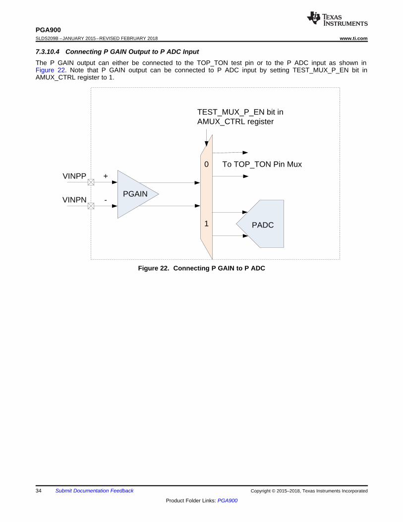
7.3.10.4 Connecting P GAIN Output to P ADC InputThe P GAIN output can either be connected to the TOP_TON test pin or to the P ADC input as shown inFigure 22. Note that P GAIN output can be connected to P ADC input by setting TEST_MUX_P_EN bit inAMUX_CTRL register to 1.
Figure 22. Connecting P GAIN to P ADC

VINTP
VINTN
+
+
-
-
To T ADC
TSEM_N
TSEM_N
MU
X
VREF = 2.5V
VOTP
VOTN
ýþ =÷üþ + ÷üü
Û+ õï÷ü×
÷üþF ÷üü
Û
ýü =÷üþ + ÷üü
ÛF õï÷ü×
÷üþF ÷üü
Û
ýñû =÷üþ+ ÷üü
Û
35
PGA900www.ti.com SLDS209B –JANUARY 2015–REVISED FEBRUARY 2018
Product Folder Links: PGA900
Submit Documentation FeedbackCopyright © 2015–2018, Texas Instruments Incorporated
7.3.11 T GainThe device has the ability to perform temperature compensation through an internal or external temperaturesensor. The user can select the source of the temperature measurement with the TEMP_MUX_CTRL bits inTEMP_CTRL register. Note that the device connects to an external temperature sensor through theVINTP/VINTN pins.
The T Gain block is constructed with a low-flicker noise, low offset, chopper-stabilized amplifier. The gain isconfigurable with 2 bits in the T_GAIN_SELECT register. Figure 23 shows the T gain amplifier topology. The gainof this stage is adjustable using 5 bits in P_GAIN_SELECT register to accommodate sensing elements withwide-range of signal spans.
Figure 23. Temperature Sensor AFE
The T Gain amplifier can be configured for single-ended or differential operation using the TSEM_N bit inAMUX_CTRL register. Note that when the T gain amplifier is set up for single-ended operation, the differentialvoltage converted by T ADC is with respect to ground. Table 2 shows the configuration that the user needs toselect for the different temperature sources.
Table 2. T Gain ConfigurationTEMPERATURE SOURCE T GAIN CONFIGURATION
Internal temperature sensor Single-endedExternal temperature sensor with one terminal of sensor connected to ground Single-endedExternal temperature sensor with neither terminal of the sensor connected to ground Differential
VOTP 0.1 V VINTP TGAIN 2 V
VOTN GND
u
9,173 9,171 9,173 ± 9,171VOTP TGAIN
2 29,173 9,171 9,173 ± 9,171
9271 ± 7*$,12 2
u
u
VINTP VINTNVOCM
292',)) 7*$,1 9,173 ± 9,171
u
VINTP VINTNVICM
29,',)) 9,173 ± 9,171
36
PGA900SLDS209B –JANUARY 2015–REVISED FEBRUARY 2018 www.ti.com
Product Folder Links: PGA900
Submit Documentation Feedback Copyright © 2015–2018, Texas Instruments Incorporated
The T Gain amplifier has to be set up for either single-ended or differential configurations depending on thesource of signal to the T Gain.
The signal to the T Gain must meet the requirements below as shown in T Gain (Chopper Stabilized):1. 0.005 V < VINTP < 1.8 V2. 0.005 V < VINTN < 1.8 V3. 0.1 V < VOTP < 2 V4. 0.1 V < VOTN < 2 V
If the signal is differential, based on the above constraints, the Input Common-Mode Voltage, VICM, and theInput Differential Voltage, VIDIFF, can be defined in :
In a similar way, the Output Common-Mode Voltage, VOCM, and the Output Differential Voltage, VODIFF, canbe defined in :
As a result, the single-ended outputs from the TGAIN, VOTP and VOTN, are defined in :
If the T Gain amplifier is setup for single-ended configuration, then the signal to the T Gain must still meet therequirements shown in T Gain (Chopper Stabilized) but in this case VINTN = GND. The equations for VOTP andVOTN then become :
NOTEWhen T GAIN is configured to measure internal temperature sensor output, T GAIN mustbe configured to operated in single-ended mode and must be configured for a gain of 5V/V.
7.3.12 T Analog-to-Digital ConverterThe T analog-to-digital converter digitizes the output of the T gain amplifier. The digitized value is available inTADC_DATA1-3 registers.
7.3.12.1 T Sigma-Delta Modulator for T ADCThe sigma-delta modulator for T ADC is a 1-MHz, second-order, 3-bit quantizer sigma-delta modulator. The Tsigma-delta modulator can be halted using the ADC_CFG_1 register.
7.3.12.2 T Decimation Filters for T ADCThe temperature signal path contains a decimation filter that can be configured to have output rate of either 64 or128 µs.
The output of the decimation filter in the temperature signal path can be configured to be either 16-bit or 24-bitsigned value. Some example decimation output codes for given differential voltages at the input of the sigma-delta modulator are shown in Table 3.
37
PGA900www.ti.com SLDS209B –JANUARY 2015–REVISED FEBRUARY 2018
Product Folder Links: PGA900
Submit Documentation FeedbackCopyright © 2015–2018, Texas Instruments Incorporated
Table 3. Input Voltage to Output Counts for T ADCSIGMA DELTA MODULATOR
DIFFERENTIAL INPUTVOLTAGE (V)
16-BIT NOISE-FREEDECIMATOR OUTPUT
24-BIT NOISE-FREE DECIMATOROUTPUT
–2.5 –32768 (0x8000) –8388608 (0x800000)–1.25 –16384 (0xC000) –4194304 (0xC00000)
0 0 (0x0000) 0 (0x000000)1.25 16383 (0x3FFF) 4194303 (0x3FFFFF)2.5 32767 (0x7FFF) 8388607 (0x7FFFFF)
The nominal relationship between the device junction temperature and 24-bit T ADC Code for T GAIN = 5 V/V isshown in Equation 1.
T ADC Code = 6632.1 × TEMP + 1710281.3,
where• TEMP is temperature in °C (1)
Table 4 shows T ADC output for some example junction temperature values.
Table 4. Internal Temperature Sensor to T ADC ValueINTERNAL TEMPERATURE 24-BIT T ADC NOMINAL VALUE
–40°C 1444997 (0x160C85)0°C 1710281 (0x1A18C9)
150°C 2705096 (0x2946C8)
7.3.12.2.1 T ADC Configuration
The T ADC can be configured using the TADC_CONFIG register as follows:1. Enable/disable: The decimation filter can be disabled.2. 16-bit/24-bit: The decimation filter can be configured to provide either 16-bit output or 24-bit output. The
decimator output is available in TADC_DATA1-3 registers3. Output rate: The decimator output rate can be configured to be either 64 or 128 µs4. Interrupt rate: The decimator can be configured to interrupt the microprocessor every sample or every fourth
sample.

VINTP
VINTN
+
-TGAIN
TADC
TEST_MUX_T_EN bit in AMUX_CTRL register
To TOP_TON Pin Mux0
1
MU
XTEMP_MUX_CTRL bits inTEMP_CTRL register
38
PGA900SLDS209B –JANUARY 2015–REVISED FEBRUARY 2018 www.ti.com
Product Folder Links: PGA900
Submit Documentation Feedback Copyright © 2015–2018, Texas Instruments Incorporated
7.3.12.3 Connecting T GAIN Output to T ADC InputThe T GAIN output can either be connected to TOP_TON test pin or can connected to T ADC input as shown inFigure 24. Note that T GAIN output can be connected to T ADC input by setting TEMP_MUX_T_EN bit inAMUX_CTRL register to 1.
Figure 24. Connecting T GAIN to T ADC
7.3.13 Digital InterfacesThe digital interfaces are used to access (read and write) the internal memory spaces described in Memory.Each interface uses different pins for communication. The device has three separate modes of communication:• OWI• SPI• I2C
The three communication modes supported by PGA900 are collectively referred to as digital interfaces in thisdocument. Each communication mode has its own protocol; however, all three access the same memoryelements within the device. For all three communication modes, PGA900 device operates as a slave device.
Figure 25 shows the interface between the microprocessor, memory block, and digital interface.
All three interfaces can access the memories simultaneously. Each interface can be disabled using control bits. Itis up to the user to ensure that all three interfaces do not access the device simultaneously. Note that if securitylock is enabled in PGA900, then the digital interfaces cannot access any of the internal memories insidePGA900.

39
PGA900www.ti.com SLDS209B –JANUARY 2015–REVISED FEBRUARY 2018
Product Folder Links: PGA900
Submit Documentation FeedbackCopyright © 2015–2018, Texas Instruments Incorporated
Figure 25. Digital Interface
7.3.13.1 Accessing PGA900 Memories While Microprocessor is RunningIf the microprocessor is not in reset state, only the following registers are accessible to the digital interfaces:• MICRO_INTERFACE_CONTROL• COM_MCU_TO_DIF (which is read by digital interfaces)• COM_DIF_TO_MCU (which is written by digital interfaces)• COM_TX_STATUS
The COM_MCU_TO_DIF and COM_DIF_TO_MCU registers are used to communicate with the PGA900 usingthe digital interface while the microprocessor is running. These registers are collectively referred to as COMBUFregisters. Software must be implemented inside PGA900 so that PGA900 can communicate with the digitalinterface master using the COMBUF registers.
The digital interface master and PGA900 slave communicate with each other in the following way:1. The digital interface master writes data to the COM_DIF_TO_MCU register.2. When COM_DIF_TO_MCU is written by the digital interface master, COMBUF interrupt is generated. Note
that the COMBUF interrupt is enabled by writing 1 to COM_RXRDY_INT_EN bit in theCOM_RX_INT_ENABLE register.
3. In the COMBUF interrupt service routine, the microprocessor clears the COMBUF interrupt by writing 1 toCOM_RX_STATUS register.
4. The software then reads the COM_DIF_TO_MCU register and responds to received data by writing to theCOM_MCU_TO_DIF register.
5. The master periodically polls the COM_TX_STATUS register to determine if PGA900 has updated theCOM_MCU_TO_DIF register. The master reads the COM_MCU_TO_DIF register for the response fromPGA900 if COM_TX_STATUS register has been updated by PGA900.
The PGA900 software can be written such that PGA900 updates the COM_MCU_TO_DIF register periodicallywithout receiving a request from digital interface master. For example, the software in PGA900 can periodicallyupdate the processed pressure value. The master can read the processed pressure data periodically.
7.3.13.1.1 COMBUF Register Data Coherency
Both COM_MCU_TO_DIF and COM_DIF_TO_MCU registers are 16-bit registers. All 16-bits can be accessed inone transfer using SPI. However, because OWI and I2C are 8-bit transfers, these two interfaces require twoaccesses to receive all 16 bits. PGA900 implements data coherency schemes to maintain data coherency fortransfers from PGA900 to the digital interface master and for transfer between digital interface master toPGA900.
M0 Firmware Calculates Pressure
E.g., 0x1234
M0 firmware writes to 0x12 to COM_MCU_TO_DIF_B2
and0x34 COM_MCU_TO_DIF_B1
M0 Firmware Calculates Pressure
E.g., 0x5678
M0 Firmware Calculates Pressure
E.g., 0x9101
M0 Firmware Calculates Pressure
M0 updates COMBUF with new pressure
value
Master reads COMBUF_LSB.
DEVICE transmits 0x34
0x12 stored into shadow register
Master reads COMBUF_MSB.
DEVICE transmits 0x56 from shadow register
COM_MCU_TO_DIF_B1COM_MCU_TO_DIF_B2
07815
COM_MCU_TO_DIF_B2_SHADOW
These registers are mapped to M0 register space
M0 firmware writes to 0x56 to COM_MCU_TO_DIF_B2
and0x78 COM_MCU_TO_DIF_B1
M0 firmware writes to 0x91 to COM_MCU_TO_DIF_B2
and0x01 COM_MCU_TO_DIF_B1
Master reads COMBUF_LSB.
DEVICE transmits 0x78
0x56 stored into shadow register
This register is shadow register
REGISTERS
TIMING
Time
MASTER READ of COMBUF
COMBUF_LSBCOMBUF_MSB
40
PGA900SLDS209B –JANUARY 2015–REVISED FEBRUARY 2018 www.ti.com
Product Folder Links: PGA900
Submit Documentation Feedback Copyright © 2015–2018, Texas Instruments Incorporated
7.3.13.1.1.1 Coherency for Transfer From PGA900 to Master
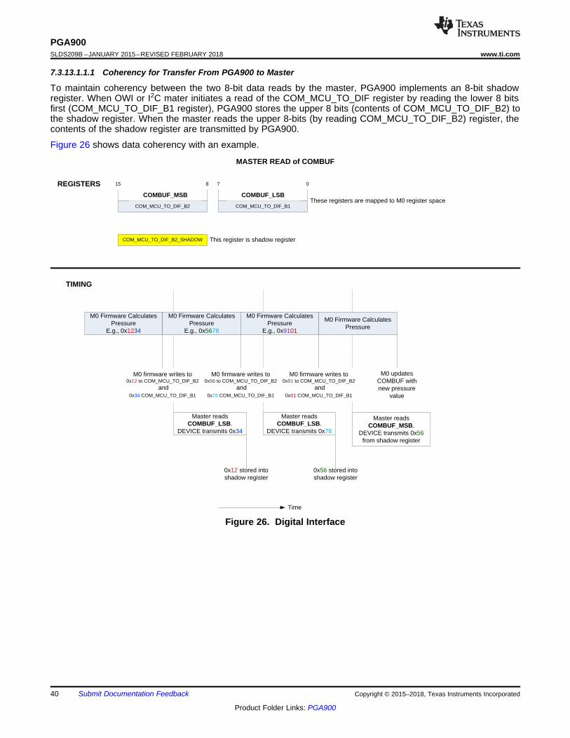
To maintain coherency between the two 8-bit data reads by the master, PGA900 implements an 8-bit shadowregister. When OWI or I2C mater initiates a read of the COM_MCU_TO_DIF register by reading the lower 8 bitsfirst (COM_MCU_TO_DIF_B1 register), PGA900 stores the upper 8 bits (contents of COM_MCU_TO_DIF_B2) tothe shadow register. When the master reads the upper 8-bits (by reading COM_MCU_TO_DIF_B2) register, thecontents of the shadow register are transmitted by PGA900.
Figure 26 shows data coherency with an example.
Figure 26. Digital Interface

Master writes to COMBUF_LSB
E.g., 0x12
No Interrupt to M0COM_RX_STATUS = 0x00COM_DIF_TO_MCU_B1 = 0x12
Master writes to COMBUF_LSB
E.g., 0x78
Master writes to COMBUF_MSB
E.g., 0x91
Master reads COM_RX_STATUS
DEVICE Reads COMBUF_LSB. Value is 0x12
DEVICE firmware reads both
COMBUF_LSB and COMBUF_MSB. DEVICE clears
COM_RX_STATUS bit to indicate data
has been read
COM_DIF_TO_MCU_B1COM_DIF_TO_MCU_B2
07815
These registers are mapped to M0 register space
No Interrupt to M0COM_RX_STATUS = 0x00COM_DIF_TO_MCU_B1 = 0x78
Interrupt to M0COM_RX_STATUS=0x01 COM_MCU_TO_DIF_B2 = 0x91 COM_MCU_TO_DIF_B1=0x78
REGISTERS
TIMING
Time
DEVICE READ OF COMBUF
COM_RX_STATUS
Master reads 0x01
Master reads COM_RX_STATUS
Master reads 0x00
Master can write COM_DIF_TO_MCU
Register
COMBUF_LSBCOMBUF_MSB
41
PGA900www.ti.com SLDS209B –JANUARY 2015–REVISED FEBRUARY 2018
Product Folder Links: PGA900
Submit Documentation FeedbackCopyright © 2015–2018, Texas Instruments Incorporated
7.3.13.1.1.2 Coherency for Transfer From Master to PGA900
To maintain coherency between the two 8-bit data reads by PGA900, COMBUF interrupt is generated only whenthe digital interface master writes to upper 8 bits of the COM_DIF_TO_MCU register (that is, when the masterwrites to COM_DIF_TO_MCU_B2 register).
Figure 27 shows data coherency with an example.
Figure 27. Digital Interface
7.3.13.2 Accessing PGA900 Memories While Microprocessor is in ResetAn alternative method to using the COMBUF registers to communicate with PGA900, is to reset the PGA900microprocessor using the digital interface and enabling digital interface access. In this mode, all memories insidePGA900 are accessible to the digital interface without the need for software inside PGA900 to supportcommunication.
The microprocessor can be put in reset state by writing 1 to MICRO_RESET bit inMICRO_INTERFACE_CONTROL register using any of the digital interfaces. Access to the digital interface isenabled by writing 1 to IF_SEL bit in MICRO_INTERFACE_CONTROL register.

42
PGA900SLDS209B –JANUARY 2015–REVISED FEBRUARY 2018 www.ti.com
Product Folder Links: PGA900
Submit Documentation Feedback Copyright © 2015–2018, Texas Instruments Incorporated
7.3.13.3 Accessing OTP, DEVRAM, and DATARAM Using 8-Bit AddressesThe size of OTP, DEVRAM, and DATARAM in PGA900 is more than 256 bytes. Each of these memories is 8-bitaddressable. To allow the digital interface to access these memories using 8-bit address, these memory spacesare organized as 256-byte pages. Table 5 lists the registers used to specify the page address for each type ofmemory.
Table 5. Registers Used to Set the AddressMEMORY TYPE READ ACCESS WRITE ACCESS
OTP OTP_PAGE_ADDR OTP_PROG_ADDRDEVRAM DEVRAM_PAGE_ADDR DEVRAM_PAGE_ADDR
DATARAM DATARAM_PAGE_ADDR DATARAM_PAGE_ADDREEPROM N/A EEPROM_PAGE_ADDRESS
To address a specific memory location, the lower 8 bits of the address have to be provided as part of the digitalinterface 8-bit address field. The remaining upper bits (5 for OTP and DEVRAM, and 2 for DATARAM) have tobe specified in the corresponding page address register. That is, to access a certain memory location, the digitalinterface has to first set the Page Address bits by writing to the corresponding Page Address register. Insummary, the following steps are required to access the memories:1. Select the page address by writing to the Page Address register using the Digital Interface Write command.2. For Writing data to memory: Send the 8-bit address (corresponding to the lower 8 bits of the memory
address) as part of the Write command.3. For Reading data from memory: Send the 8-bit address (corresponding to the lower 8 bits of the memory
address) as part of the Read command.
Note that for OTP writes, the OTP is 32-bit addressable, not 8-bit addressable. Therefore,OTP_PROG_ADDRESS has to be used to write to the OTP memory. EEPROM can be written 8 bytes at a time.EEPROM_PAGE_ADDRESS register is used to specify the 8 byte page to be written.
7.3.14 OWIThe device includes a OWI digital communication interface. The function of OWI is to enable writes to and readsfrom all memory locations inside PGA900 available for OWI access.
7.3.14.1 Overview of OWIThe OWI digital communication is a master-slave communication link in which the PGA900 operates as a slavedevice only. The master device controls when data transmission begins and ends. The slave device does nottransmit data back to the master until it is commanded to do so by the master.
The VDD pin of PGA900 is used as OWI, so that when PGA900 is embedded inside of a system module, onlytwo pins are needed (VDD and GND) for communication. The OWI master communicates with PGA900 bymodulating the voltage on VDD pin while PGA900 communicates with the master by modulating current on VDDpin. The PGA900 microprocessor has the ability to control the activation and deactivation of the OWI based uponthe OWI activation pulse driven on VDD pin.
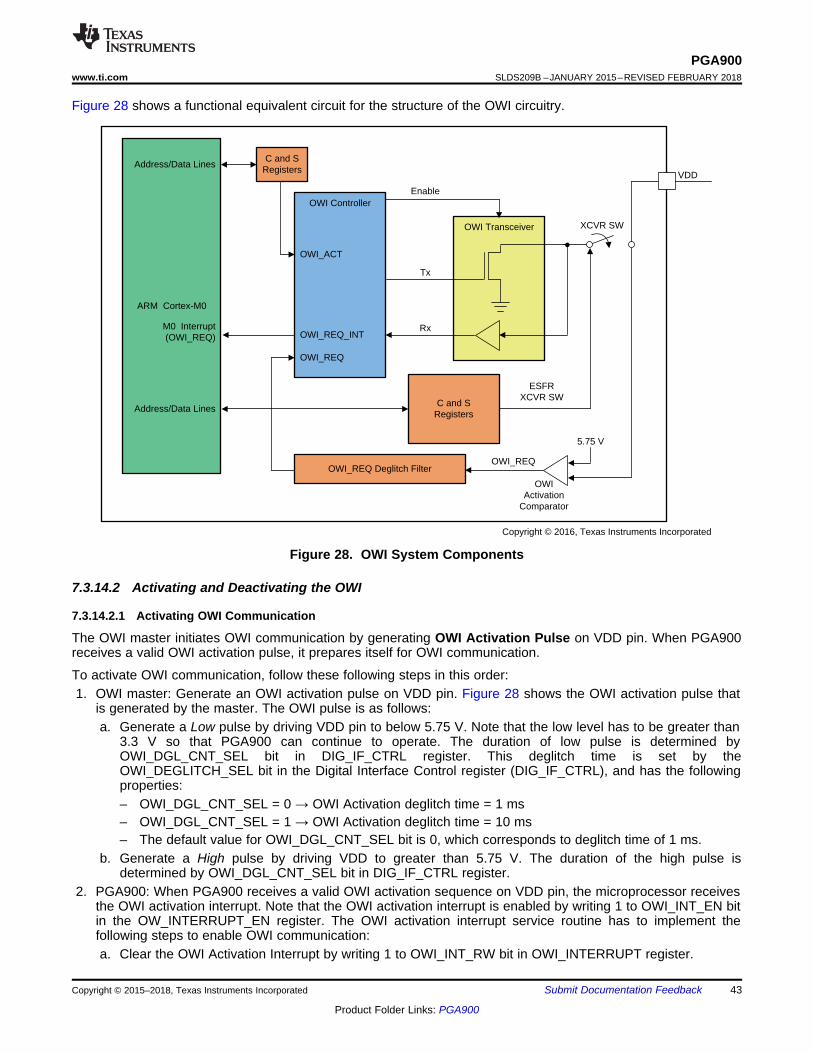
ARM Cortex-M0
Address/Data Lines
OWI Controller
M0 Interrupt(OWI_REQ)
OWI_ACT
OWI Transceiver
VDD
OWIActivation
Comparator
5.75 V
C and SRegisters
Address/Data Lines
OWI_REQ Deglitch FilterOWI_REQ
XCVR SW
C and SRegisters
Rx
Tx
Enable
ESFRXCVR SW
OWI_REQ_INT
OWI_REQ
Copyright © 2016, Texas Instruments Incorporated
43
PGA900www.ti.com SLDS209B –JANUARY 2015–REVISED FEBRUARY 2018
Product Folder Links: PGA900
Submit Documentation FeedbackCopyright © 2015–2018, Texas Instruments Incorporated
Figure 28 shows a functional equivalent circuit for the structure of the OWI circuitry.
Figure 28. OWI System Components
7.3.14.2 Activating and Deactivating the OWI
7.3.14.2.1 Activating OWI Communication
The OWI master initiates OWI communication by generating OWI Activation Pulse on VDD pin. When PGA900receives a valid OWI activation pulse, it prepares itself for OWI communication.
To activate OWI communication, follow these following steps in this order:1. OWI master: Generate an OWI activation pulse on VDD pin. Figure 28 shows the OWI activation pulse that
is generated by the master. The OWI pulse is as follows:a. Generate a Low pulse by driving VDD pin to below 5.75 V. Note that the low level has to be greater than
3.3 V so that PGA900 can continue to operate. The duration of low pulse is determined byOWI_DGL_CNT_SEL bit in DIG_IF_CTRL register. This deglitch time is set by theOWI_DEGLITCH_SEL bit in the Digital Interface Control register (DIG_IF_CTRL), and has the followingproperties:– OWI_DGL_CNT_SEL = 0 → OWI Activation deglitch time = 1 ms– OWI_DGL_CNT_SEL = 1 → OWI Activation deglitch time = 10 ms– The default value for OWI_DGL_CNT_SEL bit is 0, which corresponds to deglitch time of 1 ms.
b. Generate a High pulse by driving VDD to greater than 5.75 V. The duration of the high pulse isdetermined by OWI_DGL_CNT_SEL bit in DIG_IF_CTRL register.
2. PGA900: When PGA900 receives a valid OWI activation sequence on VDD pin, the microprocessor receivesthe OWI activation interrupt. Note that the OWI activation interrupt is enabled by writing 1 to OWI_INT_EN bitin the OW_INTERRUPT_EN register. The OWI activation interrupt service routine has to implement thefollowing steps to enable OWI communication:a. Clear the OWI Activation Interrupt by writing 1 to OWI_INT_RW bit in OWI_INTERRUPT register.

Standard field
sta
rt b
it
bit
[0]
bit
[1]
bit
[2]
bit
[3]
bit
[4]
bit
[5]
bit
[6]
bit
[7]
sto
p b
it
OWI CommunicationVDD > 5.95 VVDD > 5.95 V
VDD = 5.75 V
VDD = 4.8 V
Send OWI Activation
Interrupt to CPU
VDD = 5.95 V
10-ms(1) degltich time
10-ms(1) degltich time
VDD = 4.2 V
VDD Voltage
1. Deglitch time can be programmed to either 1 ms or 10 ms
VDD < 5.75 V
44
PGA900SLDS209B –JANUARY 2015–REVISED FEBRUARY 2018 www.ti.com
Product Folder Links: PGA900
Submit Documentation Feedback Copyright © 2015–2018, Texas Instruments Incorporated
b. Enable OWI by writing 1 to OWI_EN bit in DIG_IF_CTRL register.c. Connect OWI transceiver to VDD pin by writing 1 to the OWI_XCR_EN bit in DIG_IF_CTRL register.d. If the OWI master communicates to PGA900 with the microprocessor in reset, reset microprocessor by
writing 1 to MICRO_RESET bit in MICRO_INTERFACE_CONTROL register and enable digital interfaceby writing 1 to IF_SEL bit in the MICRO_INTERFACE_CONTROL. If OWI master communicates withPGA900 while microprocessor is running, then the COMBUF registers are used for communication.
A. Deglitch time programmed to 10 ms.
Figure 29. OWI Activation Using Overvoltage Drive
7.3.14.2.2 Deactivating OWI Communication
To deactivate OWI communication and restart the microprocessor inside PGA900 (if it was in reset), themicroprocessor reset must be de-asserted by writing 0 to MICRO_RESET bit inMICRO_INTERFACE_CONTROL register.
7.3.14.3 OWI Protocol
7.3.14.3.1 OWI Frame Structure
7.3.14.3.1.1 Standard Field Structure
Data is transmitted on the OWI in byte-sized packets. The first bit of the OWI field is the start bit. The next 8 bitsof the field are data bits to be processed by the OWI control logic. The final bit in the OWI field is the stop bit. Agroup of fields make up a transmission frame. A transmission frame is composed of the fields necessary tocomplete one transmission operation on the OWI. Figure 30 shows the standard field structure for a one-wirefield.
Figure 30. Standard OWI Field

sta
rtb
it
sto
pb
it
Sync Field
measured time
bit[0
]
bit[1
]
bit[2
]
bit[3
]
bit[4
]
bit[5
]
bit[6
]
bit[7
]
cmd[0:7] data-1[0:7] data-N[0:7]
Sync fieldCommand
Field
1st
Data
Field
Nth Data
Field
Inter-Field
Wait Time
(one bit time)
45
PGA900www.ti.com SLDS209B –JANUARY 2015–REVISED FEBRUARY 2018
Product Folder Links: PGA900
Submit Documentation FeedbackCopyright © 2015–2018, Texas Instruments Incorporated
7.3.14.3.1.2 Frame Structure
A complete one-wire data transmission operation is done in a frame with the structure shown in Figure 31.
Figure 31. OWI Transmission Frame, N = 1 to 8
Each transmission frame must have a Synchronization field and command field followed by 0 to 8 data fields.The sync field and command fields are always transmitted by the master device. The data field or fields may betransmitted either by the master or the slave depending on the command given in the command field. It is thecommand field which determines direction of travel of the data fields (master-to-slave or slave-to-master). Thenumber of data fields transmitted is also determined by the command in the command field. The inter-field waittime is optional and may be necessary for the slave or master to process data that has been received.
If OWI remains idle in either logic 0 or 1 state, for more than 15 ms, then the PGA900 communication resets andexpects to receive a sync field as the next data transmission from the master.
7.3.14.3.1.3 SYNC Field
The SYNC field is the first field in every frame that is transmitted by the master. The SYNC field is used by theslave device to compute the bit width transmitted by the master. This bit width is used to accurately receive allsubsequent fields transmitted by the master. The format of the SYNC field is shown in Figure 32.
Figure 32. OWI SYNC Field
NOTEConsecutive SYNC field bits are measured and compared to determine if a valid SYNCfield is being transmitted to the PGA900. If the difference in bit widths of any twoconsecutive SYNC field bits is greater than ±19%, then PGA900 ignores the rest of theOWI frame; that is, the PGA900 does not respond to the OWI message.
7.3.14.3.1.4 Command Field
The command field is the second field in every frame sent by the master. The command field containsinstructions about what to do with and where to send the data that is transmitted to the slave. The command fieldcan also instruct the slave to send data back to the master during a Read operation. The number of data fields tobe transmitted is also determined by the command in the command field. Figure 33 shows the format of thecommand field.
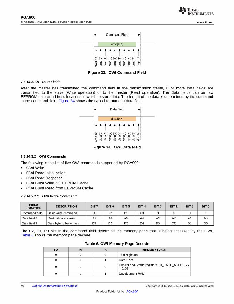
Data Field
sta
rtb
it
da
ta[0
]
da
ta[1
]
da
ta[2
]
da
ta[3
]
da
ta[4
]
da
ta[5
]
da
ta[6
]
sto
pb
it
da
ta[7
]
data[0:7]
Command Field
sta
rtb
it
cm
d[7
]
cm
d[6
]
cm
d[5
]
cm
d[4
]
cm
d[3
]
cm
d[2
]
cm
d[1
]
sto
pb
it
cm
d[0
]
cmd[0:7]
46
PGA900SLDS209B –JANUARY 2015–REVISED FEBRUARY 2018 www.ti.com
Product Folder Links: PGA900
Submit Documentation Feedback Copyright © 2015–2018, Texas Instruments Incorporated
Figure 33. OWI Command Field
7.3.14.3.1.5 Data Fields
After the master has transmitted the command field in the transmission frame, 0 or more data fields aretransmitted to the slave (Write operation) or to the master (Read operation). The Data fields can be rawEEPROM data or address locations in which to store data. The format of the data is determined by the commandin the command field. Figure 34 shows the typical format of a data field.
Figure 34. OWI Data Field
7.3.14.3.2 OWI Commands
The following is the list of five OWI commands supported by PGA900:• OWI Write• OWI Read Initialization• OWI Read Response• OWI Burst Write of EEPROM Cache• OWI Burst Read from EEPROM Cache
7.3.14.3.2.1 OWI Write Command
FIELDLOCATION DESCRIPTION BIT 7 BIT 6 BIT 5 BIT 4 BIT 3 BIT 2 BIT 1 BIT 0
Command field Basic write command 0 P2 P1 P0 0 0 0 1Data field 1 Destination address A7 A6 A5 A4 A3 A2 A1 A0Data field 2 Data byte to be written D7 D6 D5 D4 D3 D2 D1 D0
The P2, P1, P0 bits in the command field determine the memory page that is being accessed by the OWI.Table 6 shows the memory page decode.
Table 6. OWI Memory Page DecodeP2 P1 P0 MEMORY PAGE0 0 0 Test registers0 0 1 Data RAM
0 1 0 Control and Status registers, DI_PAGE_ADDRESS= 0x02
0 1 1 Development RAM

47
PGA900www.ti.com SLDS209B –JANUARY 2015–REVISED FEBRUARY 2018
Product Folder Links: PGA900
Submit Documentation FeedbackCopyright © 2015–2018, Texas Instruments Incorporated
Table 6. OWI Memory Page Decode (continued)P2 P1 P0 MEMORY PAGE1 0 0 OTP1 0 1 EEPROM cache/cells1 1 0 Reserved
1 1 1 Control and Status registers, DI_PAGE_ADDRESS= 0x07
7.3.14.3.2.2 OWI Read Initialization Command
FIELDLOCATION DESCRIPTION BIT 7 BIT 6 BIT 5 BIT 4 BIT 3 BIT 2 BIT 1 BIT 0
Command field Read Init command 0 P2 P1 P0 0 0 1 0Data field 1 Fetch address A7 A6 A5 A4 A3 A2 A1 A0
The P2, P1, P0 bits in the command field determine the memory page that is being accessed by the OWI. Thememory page decode is shown in Table 6.
7.3.14.3.2.3 OWI Read Response Command
FIELDLOCATION DESCRIPTION BIT 7 BIT 6 BIT 5 BIT 4 BIT 3 BIT 2 BIT 1 BIT 0
Command field Read response command 0 1 1 1 0 0 1 1
Data field 1 Data retrieved (OWI drivesdata out) D7 D6 D5 D4 D3 D2 D1 D0
The P2, P1, P0 bits in the command field determine the memory page that is being accessed by the OWI.Table 6 shows the memory page decode.
7.3.14.3.2.4 OWI Burst Write Command (EEPROM Cache Access)
FIELDLOCATION DESCRIPTION BIT 7 BIT 6 BIT 5 BIT 4 BIT 3 BIT 2 BIT 1 BIT 0
Command field EE_CACHE write commandcache bytes (0 to 7) 1 1 0 1 0 0 0 0
Data field 1 First data byte to be written D7 D6 D5 D4 D3 D2 D1 D0
Data field 2 Second data byte to bewritten D7 D6 D5 D4 D3 D2 D1 D0
Data field 3 Third data byte to be written D7 D6 D5 D4 D3 D2 D1 D0Data field 4 Fourth data byte to be written D7 D6 D5 D4 D3 D2 D1 D0Data field 5 Fifth data byte to be written D7 D6 D5 D4 D3 D2 D1 D0Data field 6 Sixth data byte to be written D7 D6 D5 D4 D3 D2 D1 D0
Data field 7 Seventh data byte to bewritten D7 D6 D5 D4 D3 D2 D1 D0
Data field 8 Eighth data byte to be written D7 D6 D5 D4 D3 D2 D1 D0
7.3.14.3.2.5 OWI Burst Read Command (EEPROM Cache Access)
FIELDLOCATION DESCRIPTION BIT 7 BIT 6 BIT 5 BIT 4 BIT 3 BIT 2 BIT 1 BIT 0
Command field Burst read response (8-bytes) 1 1 0 1 0 0 1 1
Data field 1 First data byte retrievedEE cache byte 0 D7 D6 D5 D4 D3 D2 D1 D0
Data field 2 Second data byte retrievedEE cache byte 1 D7 D6 D5 D4 D3 D2 D1 D0
Data field 3 Third data byte retrievedEE cache byte 2 D7 D6 D5 D4 D3 D2 D1 D0
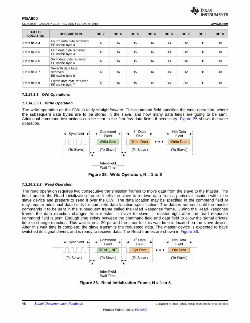
READ_INIT Opt Data Opt Data
Sync fieldCommand
Field
1st
Data
Field
Nth Data
Field
Inter-Field
Wait Time
(To Slave) (To Slave)(To Slave)(To Slave)
Write Cmd Write Data Write Data
Sync fieldCommand
Field
1st
Data
Field
Nth Data
Field
Inter-Field
Wait Time
(To Slave) (To Slave)(To Slave)(To Slave)
48
PGA900SLDS209B –JANUARY 2015–REVISED FEBRUARY 2018 www.ti.com
Product Folder Links: PGA900
Submit Documentation Feedback Copyright © 2015–2018, Texas Instruments Incorporated
FIELDLOCATION DESCRIPTION BIT 7 BIT 6 BIT 5 BIT 4 BIT 3 BIT 2 BIT 1 BIT 0
Data field 4 Fourth data byte retrievedEE cache byte 3 D7 D6 D5 D4 D3 D2 D1 D0
Data field 5 Fifth data byte retrievedEE cache byte 4 D7 D6 D5 D4 D3 D2 D1 D0
Data field 6 Sixth data byte retrievedEE cache byte 5 D7 D6 D5 D4 D3 D2 D1 D0
Data field 7Seventh data byteretrievedEE cache byte 6
D7 D6 D5 D4 D3 D2 D1 D0
Data field 8 Eighth data byte retrievedEE cache byte 7 D7 D6 D5 D4 D3 D2 D1 D0
7.3.14.3.3 OWI Operations
7.3.14.3.3.1 Write Operation
The write operation on the OWI is fairly straightforward. The command field specifies the write operation, wherethe subsequent data bytes are to be stored in the slave, and how many data fields are going to be sent.Additional command instructions can be sent in the first few data fields if necessary. Figure 35 shows the writeoperation.
Figure 35. Write Operation, N = 1 to 8
7.3.14.3.3.2 Read Operation
The read operation requires two consecutive transmission frames to move data from the slave to the master. Thefirst frame is the Read Initialization frame. It tells the slave to retrieve data from a particular location within theslave device and prepare to send it over the OWI. The data location may be specified in the command field ormay require additional data fields for complete data location specification. The data is not sent until the mastercommands it to be sent in the subsequent frame called the Read Response frame. During the Read Responseframe, the data direction changes from master → slave to slave → master right after the read responsecommand field is sent. Enough time exists between the command field and data field to allow the signal driverstime to change direction. This wait time is 20 µs and the timer for this wait time is located on the slave device.After this wait time is complete, the slave transmits the requested data. The master device is expected to haveswitched its signal drivers and is ready to receive data. The Read frames are shown in Figure 36.
Figure 36. Read Initialization Frame, N = 1 to 8

RD_RESP Read Data Read Data
Sync fieldCommand
Field
1st
Data
Field
Nth Data
Field
Inter-Field
Wait Time
(To Master) (To Master)
Data changes direction between
command field and first Data
field.
(To Slave) (To Slave)
49
PGA900www.ti.com SLDS209B –JANUARY 2015–REVISED FEBRUARY 2018
Product Folder Links: PGA900
Submit Documentation FeedbackCopyright © 2015–2018, Texas Instruments Incorporated
Figure 37. Read Response Frame, N = 1 to 8
7.3.14.3.3.3 EEPROM Burst Write
The EEPROM burst write is used to write 8 bytes of data to the EEPROM cache using one OWI frame. Thisallows fast programming of EEPROM in the manufacturing line. Note that the EEPROM page must be selectedbefore transferring the contents of the EEPROM memory cells to the EEPROM cache.
7.3.14.3.3.4 EEPROM Burst Read
The EEPROM burst read is used to read 8 bytes of data from the EEPROM cache using one OWI frame. TheBurst Read command is used for fast read the EEPROM cache contents in the manufacturing line. The readprocess is used to verify the writes to the EEPROM cache.
7.3.14.4 OWI Communication Error StatusPGA900 detects errors in OWI communication. OWI_ERROR_STATUS_LO and OWI_ERROR_STATUS_HIregisters contain OWI communication error bits. The communication errors detected include• Out of range communication baud rate• Invalid SYNC field• Invalid STOP bits in command and data• Invalid OWI command
7.3.15 SPIThe device includes a SPI digital communication interface. The main function of the SPI is to enable writes toand reads from all addresses available for SPI access.
7.3.15.1 Overview of SPISPI is a synchronous, serial, master-slave, communication standard that requires the following four pins:• MOSI: SPI master out slave in, input pin• MISO: SPI master in slave out, serial output pin (tri-state output)• SCK: SPI clock which controls the communication• CSN: Chip select (active low)
SPI communicates in a master/slave style where only one device, the master, can initiate data transmissions.The PGA900 always acts as the slave in SPI communication, where whatever external device that iscommunicating to it becomes the master. Both devices begin data transmission with the most significant bit(MSB) first.
Because multiple slave devices can exist on one bus, the master node is able to notify the specific slave nodethat it is ready to begin communicating by driving the CSN line to a low logic level. In the absence of activetransmission, the master SPI device places the device in reset by driving the CSN pin to a high logic level.During a reset state the MISO pin operates in tri-state mode. For the SPI interface to have access to memorylocations other than test register space, the IF_SEL bit in the MICRO_INTERFACE_CONTROL register has tobe set to 1.
7.3.15.2 Activating the SPITo activate SPI communication, follow these steps in this order:

Byte 1 Byte 2 Byte 3 Byte 1 Byte 2 Byte 3
0x05Data from
ADDR
Master to Slave
Slave to master
Read Command from Master
DEVICE Response to Read Command
Next Command from Master
16
15 023 7
8
Data from ADDR+1
50
PGA900SLDS209B –JANUARY 2015–REVISED FEBRUARY 2018 www.ti.com
Product Folder Links: PGA900
Submit Documentation Feedback Copyright © 2015–2018, Texas Instruments Incorporated
1. Enable SPI by writing 1 to SPI_EN bit in DIG_IF_CTRL register2. If SPI master communicates to PGA900 with the microprocessor in reset, reset microprocessor by writing 1
to MICRO_RESET bit in MICRO_INTERFACE_CONTROL register and enable digital interface by writing 1 toIF_SEL bit in the MICRO_INTERFACE_CONTROL. If SPI master communicates with PGA900 whilemicroprocessor is running, then the COMBUF registers are used for communication.
7.3.15.3 SPI Protocol
7.3.15.3.1 SPI Master to PGA900 Commands
The SPI is a 24-bit protocol with a 3-bit memory access control word, a read-write bit, an 8-bit address, and an 8-bit data word. Table 7 describes the command codes.
Table 7. SPI Command CodesBIT FUNCTION DESCRIPTION
23:21
DI PAGE ADDRESSTEST = 3’b000 Access to Control and Status registers with DI PAGE ADDRESS = 0x0
DATA RAM = 3’b001 Bits [9:8] of the Data RAM address is specified by the DATARAM_PAGE_ADDR registerBits [7:0] of the Data RAM address is specified by the Data Address field of the SPI transaction
Control and StatusRegisters = 3’b010 Access to Control and Status registers with DI PAGE ADDRESS = 0x2
DEVELOPMENT RAM= 3b011
Bits [11:8] of the Development RAM address is specified by the DEVRAM_PAGE_ADDR registerBits [7:0] of the Development RAM address is specified by the Data Address field of the SPItransaction
OTP = 3’b100 Bits [11:8] of the OTP address is specified by the OTP_PAGE_ADDR registerBits [7:0] of the OTP address is specified by the Data Address field of the SPI transaction
EECACHE = 3’b101 Access to the EEPROM cache/cellsRESERVED = 3b110RESERVED = 3b111 Access to Control and Status registers with DI PAGE ADDRESS = 0x7
20:13 Data AddressAddress of register to read or write.During Reads, bit 13 is always 0.The reads always happen to 16-bit aligned addresses.
12 Write if 1, Read if 011:4 Data3:0 Don't Care
7.3.15.3.2 PGA900 to SPI Master Response
For SPI transfers to all the memories, the read data is available on the next SPI transfer as shown in Figure 38.That is, when reading from a memory location, the user has to send a subsequent transfer to get the data back.Further, the SPI response contains 16 bits of data. The PGA900 returns data from a 16-bit aligned address; thatis, SPI reads must not straddle the 16-bit address boundary.
Figure 38. Response to SPI Read Commands is Available When the Next Command is Sent

51
PGA900www.ti.com SLDS209B –JANUARY 2015–REVISED FEBRUARY 2018
Product Folder Links: PGA900
Submit Documentation FeedbackCopyright © 2015–2018, Texas Instruments Incorporated
Table 8 describes the SPI response. Note that only 2 bytes of data can be read with one SPI read command.
Table 8. SPI ResponseBIT FUNCTION
23:20 0b000019:16 0b010115:8 Read Data from ADDR, where ADDR is received in the previous SPI command7:0 Read Data from ADDR + 1, where ADDR is received in the previous SPI command
7.3.15.3.3 SPI Command Examples
Table 9 lists a few examples of SPI transfers.
Table 9. SPI Transfers ExamplesCOMMAND MASTER TO SLAVE DATA ON SPI MOSI
Read COM_MCU_TO_DIF_B1 000 00000100 0 XXXXXXXX 0000Write 0x80 to Control and Status registers0x30 (DAC_REG0_1)
010 00110000 1 10000000 0000
Write 0x34 to Data SRAM 0x7F 1. Write 0 to DATARAM_PAGE_ADDR: 010 00011001 1 00000000 00002. Send the following command to write data: 001 01111111 1 00110100 0000
Read from EEPROM Byte 7 101 00000111 0 XXXXXXXX 0000
Write 0xD9 to DEVRAM 0x1765 1. Write 0x17 to DEVRAM_PAGE_ADDR: 010 00011010 1 00010111 00002. Send the following command to write data: 011 01100101 1 11011001 0000
7.3.15.4 Clocking Details of SPIInput data on the MOSI pin must be driven from the rising edge of the SCK clock, whereas output data on theMISO pin changes during the rising edge of the SCK clock. For SPI timing information, refer to the SPI TimingRequirements table.
7.3.16 I2C InterfaceThe device includes an I2C digital communication interface. The main function of the I2C is to enable writes toand reads from all addresses available for I2C access.
7.3.16.1 Overview of I2C InterfaceI2C is a synchronous serial communication standard that requires the following two pins for communication:• SDA: I2C serial data line (SDA)• SCL: I2C serial clock line (SCL)
In addition, CSN pin is used to select the I2C device address of PGA900. Specifically• CSN - Logic 1 - Device address - 0x20:0x27• CSN - Logic 0 - Device address - 0x40:0x47
It is noted that for valid I2C communication to occur• CSN must not change value during an I2C transaction• SPI clock (SCLK) must not be active when CSN is Logic 0 when selecting the I2C device address
I2C communicates in a master/slave style communication bus where one device, the master, can initiate datatransmission. The device always acts as the slave device in I2C communication, where the external device that iscommunicating to it acts as the master. The master device is responsible for initiating communication over theSDA line and supplying the clock signal on the SCL line. When the I2C SDA line is pulled low it is considered alogical zero, and when the I2C SDA line is floating high it is considered a logical one. For the I2C interface tohave access to memory locations other than test register space, the IF_SEL bit in theMICRO_lNTERFACE_CONTROL register has to be set to logic one.

S
SLAVE
ADDRESS
[6:0]
0 A
Register
Address
[7:0]
ADATA
[7:0]A/A P
From Master To Slave
From Slave To Master
Data Transferred
(n bytes + acknowledge)
A = acknowledge (SDA LOW)
A = not acknowledge (SDA HIGH)
S = START condition
P = STOP Condition
52
PGA900SLDS209B –JANUARY 2015–REVISED FEBRUARY 2018 www.ti.com
Product Folder Links: PGA900
Submit Documentation Feedback Copyright © 2015–2018, Texas Instruments Incorporated
7.3.16.2 Activating the I2C InterfaceTo activate I2C communication, follow these steps in order:1. Enable I2C by writing 1 to I2C_EN bit in DIG_IF_CTRL register2. If I2C master communicates to PGA900 with the microprocessor in reset, reset microprocessor by writing 1 to
MICRO_RESET bit in MICRO_INTERFACE_CONTROL register and enable digital interface by writing 1 toIF_SEL bit in the MICRO_INTERFACE_CONTROL register. If I2C master communicates with PGA900 whilemicroprocessor is running, then the COMBUF registers are used for communication.
3. The default I2C interface communication speed is 100KBPS/400KBPS. The communication speed can bechanged to 800KPBS mode by setting I2C_RATE bit to 1 in DIG_IF_CTRL register.
4. The I2C interfaces implements a deglitch filter as required by the I2C standard. The deglitch filters areenabled by default. The deglitch filter can be disabled by setting I2C_DEGLITCH_EN bit to 0 inDIG_IF_CTRL register.
7.3.16.3 I2C Interface ProtocolFigure 39 shows the basic protocol of the I2C frame for a Write operation.
Figure 39. I2C Write Operation: A Master-Transmitter Addressing a PGA900 Slave With a 7-Bit SlaveAddress
The diagram represents the data fed into or out from the I2C SDA port.
The basic data transfer is to send 2 bytes of data to the specified slave address. The first data field is the registeraddress and the second data field is the data sent or received.
The I2C slave address is used to determine which memory page is being referenced. Table 10 shows themapping of the slave address to the memory page.
Table 10. Slave AddressesSLAVE ADDRESS WHEN CSN
= 1SLAVE ADDRESS WHEN CSN
= 0 PGA900 MEMORY PAGE
0x20 0x40 Test registers0x21 0x41 Data RAM
0x22 0x42 Control and status registers,di_page_address = 0x02
0x23 0x43 Development RAM0x24 0x44 OTP0x25 0x45 EEPROM cache/cells0x26 0x46 Reserved
0x27 0x47 Control and status registers,DI_PAGE_ADDRESS = 0x07

S
SLAVE
ADDRESS
[6:0]
0 ARegister Address
[7:0]A RS
SLAVE
ADDRESS
[6:0]
1 ASlave Data
[7:0]P
From Master To Slave
From Slave To Master
A = acknowledge (SDA LOW)
S = START condition
RS = Repeat Start Condition (same as Start condition)
P = STOP Condition
53
PGA900www.ti.com SLDS209B –JANUARY 2015–REVISED FEBRUARY 2018
Product Folder Links: PGA900
Submit Documentation FeedbackCopyright © 2015–2018, Texas Instruments Incorporated
Figure 40 shows the basic PGA900 I2C protocol for a read operation.
Figure 40. I2C Read Operation: A Master-Transmitter Addressing a PGA900 Slave With a 7-Bit SlaveAddress
The slave address determines the memory page. The R/W bit is set to 0.
The register address specifies the 8-bit address of the requested data.
The repeat start condition replaces the write data from the above write operation description. This informs thePGA900 devices that Read operation is going to take place instead of a write operation.
The second slave address contains the memory page from which the data is retrieved. The R/W bit is set to 1.
Slave data is transmitted after the acknowledge is received by the master.

54
PGA900SLDS209B –JANUARY 2015–REVISED FEBRUARY 2018 www.ti.com
Product Folder Links: PGA900
Submit Documentation Feedback Copyright © 2015–2018, Texas Instruments Incorporated
Table 11 lists a few examples of I2C Transfers.
Table 11. I2C Transfers ExamplesCOMMAND MASTER TO SLAVE DATA ON I2C SDA ((CSN = 1) MASTER TO SLAVE DATA ON I2C SDA ((CSN = 0)
ReadCOM_MCU_TO_DIF_B0
Slave address: 010 0000Register address: 0000 0100
Slave address: 100 0000Register address: 0000 0100
Write 0x80 to Control andStatus Registers 0x30(DAC_REG0_1)
Slave address: 010 0010Register address: 0011 0000Data: 1000 0000
Slave address: 100 0010Register address: 0011 0000Data: 1000 0000
Write 0x34 to Data SRAM0x7F
1. Write 0 to DATARAM_PAGE_ADDR
Slave address: 010 0010
Register address 0001 1001
Data: 0000 00002. Send the following command to write data:
Slave address: 010 0001
Register address 0111 1111
Data:0011 0100
1. Write 0 to DATARAM_PAGE_ADDR
Slave address: 100 0010
Register address 0001 1001
Data: 0000 00002. Send the following command to write data:
Slave address: 100 0001
Register address 0111 1111
Data:0011 0100
Read from EEPROM Byte7
Slave Address: 010 0101Register Address: 0000 0111
Slave Address: 100 0101Register Address: 0000 0111
Write 0xD9 to DEVRAM0x1765
1. Write 0x17 to DEVRAM_PAGE_ADDR
Slave address: 010 0010
Register address: 0001 1010
Data: 0001 01112. Send the following command to write data
Slave address: 010 0011
Register address 0110 0101
Data:1101 1001
1. Write 0x17 to DEVRAM_PAGE_ADDR
Slave address: 100 0010
Register address: 0001 1010
Data: 0001 01112. Send the following command to write data
Slave address: 100 0011
Register address 0110 0101
Data:1101 1001
7.3.16.4 Clocking Details of I2C InterfaceThe device samples the data on the SDA line when the rising edge of the SCL line is high, and is changed whenthe SCL line is low. The only exceptions to this indication are a start, stop, or repeated start condition as shownin Figure 41.
Figure 41. I2C Clocking Details
7.3.17 PWM LogicThe device has PWM logic. The PWM output is available on TOPDIG or TONDIG pins as a digital output. Inaddition, the PWM output is also available as an analog output at the VOUT pin; that is, the PWM logic is used todrive the DAC GAIN buffer. The PWM functionality uses a 16-bit 4-MHz free-running timer.
7.3.17.1 PWM Logic EnableThe PWM functionality can be enabled by writing a 1 to the PWM_EN bit in PWM_EN register. This enables thefree-running timer used for PWM functionality
7.3.17.2 PWM ON and OFF TimesThe PWM ON and OFF times can be configured by writing the ON and OFF time values to PWM_ON_TIME andPWM_OFF_TIME registers, respectively. If the PWM_ON_TIME and PWM_OFF_TIME registers are updated,the updated ON and OFF times take effect at the start of next ON time.

55
PGA900www.ti.com SLDS209B –JANUARY 2015–REVISED FEBRUARY 2018
Product Folder Links: PGA900
Submit Documentation FeedbackCopyright © 2015–2018, Texas Instruments Incorporated
7.3.17.3 PWM Voltage LevelsThe voltage levels of the PWM signals are configurable. The voltage level during the PWM 0 pulse is determinedby the value in DAC_REG0 register while the voltage level during the PWM 1 pulse is determined by the value inDAC_REG1 register.
7.3.18 DAC OutputThe device includes a 14-bit digital-to-analog converter that produces an absolute output voltage with respect tothe accurate reference voltage or ratiometric output voltage with respect to the VDD supply.
When the microprocessor undergoes a reset, the DAC registers are driven to 0x000 code.
7.3.18.1 Ratiometric versus AbsoluteThe DAC output can be configured to be either in ratiometric-to-VDD mode or independent-of-VDD (or absolute)mode using the DAC_RATIOMETRIC bit in DAC_CONFIG.
NOTEIn ratiometric mode, changes in the VDD voltage result in a proportional change in theoutput voltage because the current reference for the DAC is derived from VDD.
7.3.19 DAC GainThe DAC gain buffer is a configurable buffer stage for the DAC output. The DAC gain amplifier can be configuredto operate in voltage amplification mode for voltage output or current amplification mode for 4- to 20-mAapplications. In voltage output mode, DAC Gain can be configured for a specific gain value by setting theDAC_GAIN bits in DAC_CONFIG register to a specific value. The DAC gain can be configured to one of fourpossible gain configurations using the 2-bit DAC_GAIN field.
The final stage of DAC gain is connected to Vddp and ground. This gives the ability to drive VOUT voltage closeto VDD voltage.
The DAC gain buffer also implements a COMP pin to allow implementation of compensation when driving largecapacitive loads.
7.3.19.1 Connecting DAC Output to DAC GAIN InputThe DAC output can either be connected to TOP_TON test pin or can connected to DAC GAIN input as shown inFigure 42. The figure shows that the output is connected to DAC GAIN input only when TEST_MUX_DAC_EN bitin AMUX_CTRL register is set to 1.

DACGAIN
DAC
TEST_MUX_DAC_EN bit in AMUX_CTRL register
To TOP_TON Pin Mux0
1VOUT
40K +
M0
DA
C_R
EG
0D
AC
_RE
G1
DAC_EN = 1OR
PWM_EN = 0
DAC_ENABLE and PWM_EN bits control this MUX
DAC_EN = 0AND
PWM_EN = 1
56
PGA900SLDS209B –JANUARY 2015–REVISED FEBRUARY 2018 www.ti.com
Product Folder Links: PGA900
Submit Documentation Feedback Copyright © 2015–2018, Texas Instruments Incorporated
The figure also shows how the PWM logic is enabled to drive DAC GAIN. Specifically, if PWM_EN bit inPWM_EN register is set to 1 and DAC_ENABLE bit in DAC_CTRL_STATUS register is set to 0, then DAC GAINoutput is PWM output. In all other cases, the DAC GAIN output is a constant output based on the value ofDAC_REG0 register.
Figure 42. Connecting DAC to DAC GAIN
7.3.20 General-Purpose Input/Output (GPIO) and UART
7.3.20.1 GPIOThe device includes two general-purpose digital input/output pins. The two GPIO pins can be independentlyconfigured as input or output pins using the GPIO1_DIR bit in GPIO_DIR register for GPIO1 pin and GPIO2_DIRbit in GPIO_DIR register for GPIO2 pin. When configured as an output pin, the output buffers can be configuredin either open-drain output mode or push-pull output mode using the GPIO1_CFG bit in GPIO_DIR register forGPIO1 and GPIO2_CFG bit in GPIO_DIR register for GPIO2 pin.
The microprocessor reads the state of the GPIO1 pin using the GPIO1_I bit in GPIO_INPUT register. Similarly,the state of GPIO2 pin is read using the GPIO2_I bit in GPIO_INPUT register. The state of the GPIO pins can beread in both GPIO input and output configurations.
When GPIO1/GPIO2 pins are configured as output pins, the microprocessor controls the Output state by writingthe desired value to GPIO1_O bit in GPIO_OUTPUT register for GPIO1 pin and GPIO2_O bit in GPIO_OUTPUTregister for GPIO2 pin.
7.3.20.2 UARTPGA900 includes a general-purpose UART with configurable baud rate. The UART transmit and receive pins areshared with MOSI and MISO SPI pins. By default, these pins are configured for SPI functionality. The MOSI andMISO pins can be configured for UART functionality by writing 1 to UART_SEL bit in the PIN_MUX register.
The UART functionality is disabled on power up. The UART functionality can be enabled by writing 1 toUART_EN bit in UART_EN register. The communication baud rate can be configured by writing the desired baudrate to BAUD_RATE registers. The formula to calculate the value to be loaded into BAUD_RATE register is givenin Equation 2:
BAUD_RATE = round(250000 / (Desired baud rate) – 1) (2)
The UART in PGA900 is capable of transferring 8 bits only. Furthermore, the UART can be configured for evenparity, odd parity, or parity disabled by writing to the corresponding bits in UART_CFG register. The number ofstop bits is also configurable to either 1 or 2 bits using the TWO_STOP_BITS bit in the UART_CFG register. TheUART in PGA900 always transmits 1 start bit.

57
PGA900www.ti.com SLDS209B –JANUARY 2015–REVISED FEBRUARY 2018
Product Folder Links: PGA900
Submit Documentation FeedbackCopyright © 2015–2018, Texas Instruments Incorporated
The UART can be configured to generate interrupt to the microprocessor on TX Complete by writing 1 to theUART_TXCOMPLETE_INT_EN bit in UART_INTERRUPT_ENABLE register. Similarly, the UART can beconfigured to generate interrupt to the microprocessor on RX Ready by writing 1 to UART_RXRDY_INT_EN bitin UART_INTERRUPT_ENABLE register. Both TX Complete and RX Ready generate a common interrupt to themicroprocessor. The source of the interrupt has to be determined in software by reading theUART_INTERRUPT_STATUS register.
Note that the interrupt status bit has to cleared in the interrupt service routine by writing 1 toUART_TX_COMPLETE_I for TX Complete interrupt and UART_RXRDY_I bit for RX Ready interrupt inUART_INTERRUPT_STATUS register.
PGA900 initiates transmission of data over UART TX line by writing data to the UART_TX_BUF. When datatransmission is complete, TX Complete interrupt is generated. The data received on UART RX pin is stored inUART_RX_BUF. RX Ready interrupt is generated when data is received by PGA900.
The error status of UART communication is available in UART_LINE_STATUS register. See the description ofthe register for description of communication errors detected by the UART in PGA900.
7.3.21 Memory
7.3.21.1 OTP MemoryThe OTP Memory space is 8 KB. This memory space contains program instructions for the M0 microprocessor.To program the OTP memory, an external VP_OTP voltage needs to be applied to the VP_OTP pin.
The device has the ability to lockout access to all memory spaces from the digital interface. This allows users toprotect firmware intellectual property.
7.3.21.1.1 OTP Programming Using SPI
The OTP memory is programmed 4 bytes at a time. The program address is 4-byte aligned. That is, the OTPmemory can be programmed starting at location 0x0000 4 bytes at a time. To program OTP memory, the 4 bytesto be programmed have to be first loaded into OTP Data registers. The upper 12 bits of the 14-bit 4-byte alignedOTP memory address (that is, the least two significant bits of the OTP memory address have to be 0), then hasto be loaded into the program register. When the OTP_PROG bit in OTP_PROG_ADDR_2 register is set, thecontents of the OTP data registers are transferred to the OTP memory cells.
The following sequence is an example to program 0x12345678 to OTP memory address 0x1764 (which is 4-bytealigned) using SPI digital interface:1. Write 0x78 to OTP_PROG_DATA_1 register:
010 00010000 1 01111000 00002. Write 0x56 to OTP_PROG_DATA_2 register:
010 00010001 1 01010110 00003. Write 0x34 to OTP_PROG_DATA_3 register:
010 00010010 1 00110100 00004. Write 0x12 to OTP_PROG_DATA_4 register:
010 00010011 1 00010010 00005. Write 0xD9 (Least Significant Byte of (0x1764 >> 2)) to OTP_PROG_ADDR_1 register:
010 00010100 1 11011001 00006. Write 0x85 (0x05 is the Most Significant Byte of (0x1764 >> 2)) to OTP_PROG_ADDR_2 register:
010 00010101 1 10000101 00007. Read OTP_PROG_CTRL_STAT register:
010 00010110 0 xxxxxxxx 0000
Wait for bit 1 of the read data to be 0 to confirm that the OTP has been programmed if necessary.

58
PGA900SLDS209B –JANUARY 2015–REVISED FEBRUARY 2018 www.ti.com
Product Folder Links: PGA900
Submit Documentation Feedback Copyright © 2015–2018, Texas Instruments Incorporated
The programming sequence shows that six 24-bit commands must be transmitted to PGA900 to program 4 bytesof OTP. At 1 MHz, this translates to 144 µs. In addition, the SPI protocol requires 4 µs of chip select disable timebetween two consecutive commands and setup and hold times as shown in the SPI timing diagram, Figure 4.Thus, the total time to transmit 4 bytes of OTP data is 144 + (6 × 4) + 6(1) = 174 µs. To program all 8 KB, thetotal time is 174 × 8192 / 4 = 356.352 ms.
7.3.21.2 OTP Programming Using I2CThe OTP memory is programmed 4 bytes at a time. The program address is 4-byte aligned. That is, the OTPmemory can be programmed starting at location 0x0000 4 bytes at a time. To program OTP memory, the 4 bytesto be programmed have to be first loaded into OTP Data registers. The upper 12 bits of the 14-bit 4-byte alignedOTP memory address (that is, the least two significant bits of the OTP memory address have to be 0) then hasto be loaded into the program register. When the OTP_PROG bit in OTP_PROG_ADDR_2 register is set, thecontents fo the OTP data registers are transferred to the OTP memory cells.
The following sequence is an example to program 0x12345678 to OTP memory address 0x1764 (which is 4-bytealigned) using I2C digital interface assuming CSN = 1:1. Write 0x78 to OTP_PROG_DATA_1 register:
– Slave address: 0100010– Register address : 00010000– Write data : 01111000
2. Write 0x56 to OTP_PROG_DATA_2 register:– Slave address: 0100010– Register address : 00010001– Write data : 01010110
3. Write 0x34 to OTP_PROG_DATA_3 register:– Slave address: 0100010– Register address : 00010010– Write data : 00110100
4. Write 0x12 to OTP_PROG_DATA_4 register:– Slave address: 0100010– Register address : 00010011– Write data : 00010010
5. Write 0xD9 (least significant byte of (0x1764 >> 2)) to OTP_PROG_ADDR_1 register:– Slave address: 0100010– Register address : 00010100– Write data : 11011001
6. Write 0x85 (0x05 is the most significant byte of (0x1764 >> 2), OTP_PROG = 1) to OTP_PROG_ADDR_2register:– Slave address: 0100010– Register address : 00010101– Write data : 10000101
7. Read OTP_PROG_CTRL_STAT register:– Slave address: 0100010– Register address : 00010110
Wait for bit 1 of the read data to be 0 to confirm that the OTP has been programmed if necessary.
7.3.21.3 EEPROM MemoryFigure 43 shows the EEPROM structure. The contents of each EEPROM must be transferred to the EEPROMcache before writes; that is, the EEPROM can be programmed 8 bytes at a time. The EEPROM reads occurwithout the EEPROM cache.

ARM CORTEX-M0
SPI
I2C
OWI
Digital Interface
EEPROM MEMORY
CELLS
(128 Bytes16 X 64 Bits)
EEPROMCache
(8 Bytes1 X 64 Bits)
EEPROM PROGRAMDATA_Out[63:0]
CacheAddress[3:0]
ReadData_out[7:0]
Cache WriteData_In[7:0]
Interface
Mux
SERIAL
DEBUG
ReadData_out[31:0]
59
PGA900www.ti.com SLDS209B –JANUARY 2015–REVISED FEBRUARY 2018
Product Folder Links: PGA900
Submit Documentation FeedbackCopyright © 2015–2018, Texas Instruments Incorporated
Figure 43. Structure of EEPROM Interface
7.3.21.3.1 EEPROM Cache
The EEPROM cache serves as temporary storage of data being transferred to selected EEPROM locationsduring the programming process.
7.3.21.3.2 EEPROM Programming Procedure
For programming the EEPROM, the EEPROM is organized in 16 pages of 8 bytes each. The EEPROM memorycells are programmed by writing to the 8-byte EEPROM cache. The contents of the cache are transferred toEEPROM memory cells by selecting the EEPROM memory page.1. Select the EEPROM page by writing the upper 4 bits of the 7-bit EEPROM address to
EEPROM_PAGE_ADDRESS register.2. Load the 8-byte EEPROM cache by writing to the EEPROM_CACHE registers. Note that all 8 bytes have to
be loaded into the EEPROM_CACHE.3. Set the ERASE_AND_PROGRAM bit in EEPROM_CTRL register. Setting this bit automatically erases the
selected EEPROM memory page and programs it with the contents of EEPROM_CACHE. Alternatively, theuser can erase by writing 1 to the ERASE bit in EEPROM_CTRL register following by writing 1 to thePROGAM bit in the EEPROM_CTRL register after the erase is complete. The status of erase and programcan be monitored through the EEPROM_STATUS register.
7.3.21.3.3 EEPROM Programming Current
The EEPROM programming process results in an additional 6-mA current on the VDD pin for the duration ofprogramming.

60
PGA900SLDS209B –JANUARY 2015–REVISED FEBRUARY 2018 www.ti.com
Product Folder Links: PGA900
Submit Documentation Feedback Copyright © 2015–2018, Texas Instruments Incorporated
7.3.21.3.4 CRC
The last byte of the EEPROM memory is reserved for the CRC. This CRC value covers all data in the EEPROMmemory. Every time the last byte is programmed, the CRC value is automatically calculated and validated. Thevalidation process checks the calculated CRC value with the last byte programmed in the EEPROM memory cell.If the calculated CRC matches the value programmed in the last byte, the CRC_GOOD bit is set inEEPROM_CRC_STATUS register.
The CRC check can also be initiated at any time by setting the CALCULATE_CRC bit in the EEPROM_CRCregister. The status of the CRC calculation is available in the CRC_CHECK_IN_PROG bit inEEPROM_CRC_STATUS register, while the result of the CRC validation is available in the CRC_GOOD bit inEEPROM_CRC_STATUS register.
The CRC calculation pseudo code is as follows:currentCRC8 = 0xFF; // Current value of CRC8
for NextData
D = NextData;
C = currentCRC8;
begin
nextCRC8_BIT0 = D_BIT7 ^ D_BIT6 ^ D_BIT0 ^ C_BIT0 ^ C_BIT6 ^ C_BIT7;
nextCRC8_BIT1 = D_BIT6 ^ D_BIT1 ^ D_BIT0 ^ C_BIT0 ^ C_BIT1 ^ C_BIT6;
nextCRC8_BIT2 = D_BIT6 ^ D_BIT2 ^ D_BIT1 ^ D_BIT0 ^ C_BIT0 ^ C_BIT1 ^ C_BIT2 ^ C_BIT6;
nextCRC8_BIT3 = D_BIT7 ^ D_BIT3 ^ D_BIT2 ^ D_BIT1 ^ C_BIT1 ^ C_BIT2 ^ C_BIT3 ^ C_BIT7;
nextCRC8_BIT4 = D_BIT4 ^ D_BIT3 ^ D_BIT2 ^ C_BIT2 ^ C_BIT3 ^ C_BIT4;
nextCRC8_BIT5 = D_BIT5 ^ D_BIT4 ^ D_BIT3 ^ C_BIT3 ^ C_BIT4 ^ C_BIT5;
nextCRC8_BIT6 = D_BIT6 ^ D_BIT5 ^ D_BIT4 ^ C_BIT4 ^ C_BIT5 ^ C_BIT6;
nextCRC8_BIT7 = D_BIT7 ^ D_BIT6 ^ D_BIT5 ^ C_BIT5 ^ C_BIT6 ^ C_BIT7;
end
currentCRC8 = nextCRC8_D8;
endfor
NOTEThe EEPROM CRC calculation is complete 340 µs after digital core starts running atpower up. After the CRC calculation completes, the EEPROM_CRC_VALUE contains theCRC value calculated and CRC_GOOD bit in the EEPROM_CRC_STATUS registerindicates the status of the CRC check.
7.3.21.4 DATA RAM MemoryThis memory space is used for M0 scratchpad memory, such as intermediate calculation results. It is a 1-KBmemory space, and located at memory page 1.
7.3.21.5 Control and Status Registers MemoryThe M0 uses control and data registers to interact with the analog blocks of the device.

61
PGA900www.ti.com SLDS209B –JANUARY 2015–REVISED FEBRUARY 2018
Product Folder Links: PGA900
Submit Documentation FeedbackCopyright © 2015–2018, Texas Instruments Incorporated
7.3.21.6 Software Development RAM
7.3.21.6.1 Software Development
PGA900 has 8 KB of development RAM that can overlay the OTP memory address. This is to allow convenientdevelopment of software. The software development RAM can be configured to either overlay the OTP memoryaddress space (that is, same address space as OTP) or assigned to non-OTP-overlay address space using theREMAP bit in the REMAP register. The REMAP can be set using a debugger.
7.3.21.6.1.1 Downloading Software into Development RAM Using Digital Interface
Follow these steps to download the software into development RAM.1. Set REMAP bit in REMAP register to 0.2. Select the development RAM page address by writing the appropriate page value to the
DEVRAM_PAGE_ADDR register. Note that this register is at digital interface memory page address 0x02and each development RAM page consists of 256 bytes.
3. Write to the development RAM to the byte in the 256-byte development RAM page at digital interfacememory page address 0x03.
7.3.21.6.2 Trace FIFO
The PGA900 software development RAM can also be used as trace FIFO. The trace feature allows either P ADCvalue or T ADC value to be stored in the development RAM for post-processing. The trace source can beselected by setting the TRACE_SOURCE in the TRACE_FIFO_CTRL_STAT register. The trace function can beenabled by writing 1 to the TRACE_FIFO_ENABLE bit in TRACE_FIFO_CTRL_STAT register.
The trace capture stops after collecting 2048 ADC samples. The samples are 32-bit address aligned with theADC value in the lower 16 or 24 bits depending on the configured number of ADC bits. The state of tracing canbe monitored through TRACE_FIFO_EMPTY, TRACE_FIFO_HALF_FULL, and TRACE_FIFO_FULL bits in theTRACE_FIFO_CTRL_STAT register. Once the trace FIFO is enabled, a time equal to 2048 ADC samples × theconfigured decimation rate has to elapse before attempting to read the data or check the status of tracingthrough the TRACE_FIFO_CTRL_STAT register.
NOTEIf the trace feature is enabled, the software development RAM cannot be used to overlaythe OTP for software development.
7.3.21.7 OTP Security
7.3.21.7.1 Definition of OTP Security
OTP security is defined as the inability to read OTP memory contents with digital interfaces (SPI, I2C, and OWI)and software debugger. This feature is implemented in PGA900 to prevent the download of OTP contents afterthe device is deployed in the field.
7.3.21.7.2 OTP Security in PGA900
In PGA900, if OTP security is enabled, access to all memories is disabled. That is, after security is enabled, thedigital interface cannot access OTP, EEPROM, and RAM through digital interfaces and debugger.
However, the COMBUF register is accessible even when security is enabled.
7.3.21.7.3 Enabling OTP Security in PGA900
PGA900 has two registers to enable OTP security:1. SECLOCK register (8 bits)
a. Writing 0x00 enables access to all memories through digital interface.b. Writing 0xAA disables access to all memories through digital interface.
The reset value of the register is such that OTP security is disabled.2. DEBUG_LOCK bit in MICRO_INTERFACE_CONTROL register
62
PGA900SLDS209B –JANUARY 2015–REVISED FEBRUARY 2018 www.ti.com
Product Folder Links: PGA900
Submit Documentation Feedback Copyright © 2015–2018, Texas Instruments Incorporated
a. Writing a 0 to this bit enables access through software debugger.b. Writing a 1 to this bit disables access through software debugger.
The reset value of the bit is 0.
7.3.21.7.4 Using OTP Security in PGA900
The M0 firmware enables OTP security by checking a EEPROM bit (or bits) reserved for OTP security. Thissoftware is executed at M0 startup after M0 reset is deasserted. The pseudocode is:1. If (Security bit reserved in EEPROM is 1)
a. SECLOCK = 0xAA;b. DEBUG_LOCK bit = 1;
2. Elsea. SECLOCK = 0x00;b. DEBUG_LOCK bit = 0;
3. End
Using this method, if OTP security is enabled in the manufacturing line before calibration is complete, then allaccesses to memories are disabled. That is, the manufacturing tester cannot communicate with PGA900anymore. Hence, OTP security cannot be disabled. Therefore, OTP security must be enabled as a last stepon the manufacturing line.
7.3.21.7.5 Sequence in Manufacturing Line1. Ensure EEPROM bits reserved for EEPROM security correspond to OTP Security Disable value.2. Program OTP with firmware.3. Perform all calibrations.4. As a final step on the manufacturing line, program EEPROM bits corresponding to OTP security to OTP
Security Enable value.
7.3.22 DiagnosticsThis section describes the diagnostics.
7.3.22.1 Power Supply DiagnosticsThe device includes modules to monitor the power supply for faults. The internal power rails that are monitoredare:1. AVDD voltage, thresholds are generated using inaccurate reference.2. DVDD voltage, thresholds are generated using inaccurate reference.3. Bridge supply voltage, thresholds are generated using internal voltage reference.4. Internal oscillator supply voltage, thresholds are generated using inaccurate reference.5. Reference output voltage, thresholds are generated using inaccurate reference.
The electrical specifications list the voltage thresholds for each of the power rails.
When a fault is detected, an appropriate bit in the PSMON1 and PSMON2 registers is set. If the faulty conditionis removed, the fault bits remain latched. To remove the fault, M0 software must read the fault bit and write alogic zero back to the bit. In addition, a system reset clears the fault.
NOTEWhen bridge supply over voltage condition is detected, the user must disable the bridgesupply the user by setting BRDG_EN bit BRDG_CTRL register to 0. In addition, the usermust set disconnect P gain amplifier from VINPP and VINPN input pins by settingPGAIN_OPEN bit in AFE_CFG register to 1 to not damage P Gain amplifier.

63
PGA900www.ti.com SLDS209B –JANUARY 2015–REVISED FEBRUARY 2018
Product Folder Links: PGA900
Submit Documentation FeedbackCopyright © 2015–2018, Texas Instruments Incorporated
7.3.22.2 Resistive Bridge Sensor and Temperature Sensor Connectivity Diagnostics
7.3.22.2.1 P Gain Input Faults
The device includes modules to monitor for sensor faults. Specifically, the device monitors the sensor pins foropens (including loss of connection from the sensor), short-to-ground, and short to sensor supply.
When a fault is detected, an appropriate bit in the AFEDIAG register is set. All three types of sensor faults resultin the setting of the same bit, meaning it is not possible to distinguish the type of fault that has occurred. Evenafter the faulty condition is removed, the fault bits remains latched. To remove the fault the M0 software mustread the fault bit and write a logic zero back to the bit. In addition a system reset clears the fault.
Open sensor faults are detected through the use of an internal pulldown resistor. The value of the resistor andthe threshold can be configured using DIS_R1M and DIS_R2M bits in AFEDIAG_CFG register. Note that thesediagnostics can be disabled by writing to the DIS_R_SD bit in AFEDIAG_CFG register.
The thresholds for both P Gain are derived off of VBRDG voltage.

VINPP
VINPN
OV
VINP_OV
P GAIN (5 Bits)
OV
UV
VINP_UV
UV
To P ADC
VINTP
VINTN
OV
VINT_OV
T GAIN (5 Bits)
OV
To T ADC
AVDD
PGAIN_OPEN
64
PGA900SLDS209B –JANUARY 2015–REVISED FEBRUARY 2018 www.ti.com
Product Folder Links: PGA900
Submit Documentation Feedback Copyright © 2015–2018, Texas Instruments Incorporated
Figure 44. Block Diagram of P Gain and T Gain Diagnostics

65
PGA900www.ti.com SLDS209B –JANUARY 2015–REVISED FEBRUARY 2018
Product Folder Links: PGA900
Submit Documentation FeedbackCopyright © 2015–2018, Texas Instruments Incorporated
NOTEWhen an overvoltage fault is detected at the input of P gain amplifier, the user must setdisconnect P gain amplifier from VINPP and VINPN input pins by setting PGAIN_OPEN bitin AFE_CFG register to 1 in order to not damage the P gain amplifier.
7.3.22.2.2 T Gain Input Faults
The device implements a comparator to detect overvoltage conditions at the input of T gain amplifier; that is,VINTP and VINTN pins. This diagnostics can be disabled by writing to the DIS_R_TEMP bit in AFEDIAG_CFGregister.
7.3.22.3 P Gain and T Gain Output DiagnosticsThe device includes modules that verify that the output signal of each gain is within a certain range. This ensuresthat gain stages in the signal chain are working correctly. AVDD voltage is used to generate the thresholdsvoltages for comparison.
When a fault is detected, the corresponding bit in AFEDIAG register is set. Even after the faulty condition isremoved, the fault bits remain latched. To remove the fault, M0 software must read the fault bit and write a logiczero back to the bit. In addition a system reset clears the fault.

VINPP
VINPN
OV
PGAIN_OV
P GAIN (5 Bits)
OV
UV
PGAIN_UV
UV
To P ADC
VINTP
VINTN
OV
TGAIN_OV
T GAIN (2 Bits)
OV
UV
TGAIN_UV
UV
To T ADC
66
PGA900SLDS209B –JANUARY 2015–REVISED FEBRUARY 2018 www.ti.com
Product Folder Links: PGA900
Submit Documentation Feedback Copyright © 2015–2018, Texas Instruments Incorporated
Figure 45. Block Diagram of P Gain and T Gain Output Diagnostics
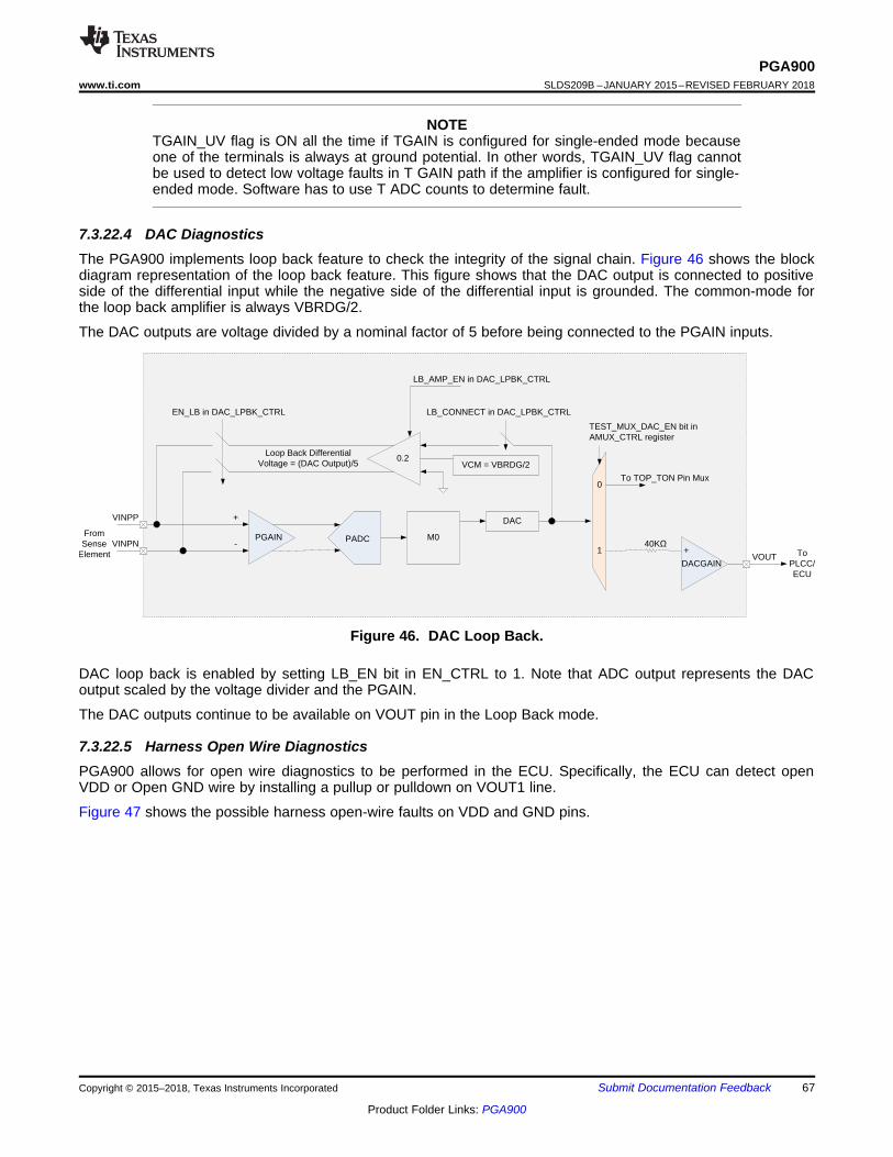
M0
DACVINPP
VINPN
VOUT
From Sense
Element To PLCC/ECU
+
-
EN_LB in DAC_LPBK_CTRL
PGAIN PADC
DACGAIN
TEST_MUX_DAC_EN bit in AMUX_CTRL register
To TOP_TON Pin Mux0
140K
+
0.2
LB_CONNECT in DAC_LPBK_CTRL
Loop Back Differential Voltage = (DAC Output)/5
LB_AMP_EN in DAC_LPBK_CTRL
VCM = VBRDG/2
67
PGA900www.ti.com SLDS209B –JANUARY 2015–REVISED FEBRUARY 2018
Product Folder Links: PGA900
Submit Documentation FeedbackCopyright © 2015–2018, Texas Instruments Incorporated
NOTETGAIN_UV flag is ON all the time if TGAIN is configured for single-ended mode becauseone of the terminals is always at ground potential. In other words, TGAIN_UV flag cannotbe used to detect low voltage faults in T GAIN path if the amplifier is configured for single-ended mode. Software has to use T ADC counts to determine fault.
7.3.22.4 DAC DiagnosticsThe PGA900 implements loop back feature to check the integrity of the signal chain. Figure 46 shows the blockdiagram representation of the loop back feature. This figure shows that the DAC output is connected to positiveside of the differential input while the negative side of the differential input is grounded. The common-mode forthe loop back amplifier is always VBRDG/2.
The DAC outputs are voltage divided by a nominal factor of 5 before being connected to the PGAIN inputs.
Figure 46. DAC Loop Back.
DAC loop back is enabled by setting LB_EN bit in EN_CTRL to 1. Note that ADC output represents the DACoutput scaled by the voltage divider and the PGAIN.
The DAC outputs continue to be available on VOUT pin in the Loop Back mode.
7.3.22.5 Harness Open Wire DiagnosticsPGA900 allows for open wire diagnostics to be performed in the ECU. Specifically, the ECU can detect openVDD or Open GND wire by installing a pullup or pulldown on VOUT1 line.
Figure 47 shows the possible harness open-wire faults on VDD and GND pins.

SENSOR ECU
VDD
VOUT1
GND
Open Wire Diagnostic 1: VDD Open, VOUT has pull up
SENSOR ECU
VDD
VOUT1
GND
Open Wire Diagnostic 2: GND Open, VOUT has pull up
SENSOR ECU
VDD
VOUT1
GND
Open Wire Diagnostic 3: VDD Open, VOUT has pull down
SENSOR ECU
VDD
VOUT1
GND
Open Wire Diagnostic 4: GND Open, VOUT has pull down
68
PGA900SLDS209B –JANUARY 2015–REVISED FEBRUARY 2018 www.ti.com
Product Folder Links: PGA900
Submit Documentation Feedback Copyright © 2015–2018, Texas Instruments Incorporated
Figure 47. Harness Open-Wire Diagnostics
CAUTIONIf FBN pin has intermittent disconnects, that is, the pin opens and reconnects, then thereconnect action could damage the device.
7.3.22.6 Software WatchdogPGA900 includes a software watchdog. The software watchdog can be enabled by writing 1 to WDOG_EN bit inthe WDOG_CTRL_STAT register. If the software watchdog is enabled software has to service the watchdogperiodically by writing to the WDOG_TRIG register.
The value written to the WDOG_TRIG corresponds to the timeout value. The timeout value:(WDOG_TRIG+1)*2ms. If the software does not service the watchdog before timeout value, the microprocessoris reset. In this case of microprocessor reset, all peripherals (including the digital interfaces) except the softwarewatchdog are reset. That is, all control and status registers are set to their respective reset values, and thesoftware watchdog continues to be enabled. Furthermore, the WD_RESET bit in WDOG_CTRL_STAT is be setto 1 to indicate that the microprocessor recovered from a software watchdog timeout event. The WD_RESET bitcan be cleared by writing a 1 to the WD_RESET bit.
7.3.22.7 EEPROM CRC and TRIM ErrorThe last Byte in the EEPROM stores the CRC for all the data in EEPROM.
The user can verify the EEPROM CRC at any time. When the last byte is loaded into the Cache, the deviceautomatically calculates the CRC and updates the CRC_ERR bit in EE_STATUS Control and Data Registers.The validity of the CRC can also be verified by initiating the CRC check by setting the control bitCACULATE_CRC bit in EEPROM_CRC register.

69
PGA900www.ti.com SLDS209B –JANUARY 2015–REVISED FEBRUARY 2018
Product Folder Links: PGA900
Submit Documentation FeedbackCopyright © 2015–2018, Texas Instruments Incorporated
The device also has analog trim values. The validity of the analog trim values is checked on power up and beforethe M0 reset is de-asserted. The validity of the trim values can be inferred using the TRIM_ERR bit inEE_STATUS Control and Data Registers.
7.3.22.8 DATA RAM MBISTThe device implements DATA RAM memory built-in self-test (MBIST). This diagnostic checks the integrity of theinternal RAM on an on-demand basis.
The procedure to start this diagnostic and check for status is as below:• 1. Set DATARAM_MBIST_CTRL bits in RAM_MBIST_CONTROL register to 0b11. This starts the DATARAM
MBIST.• 2. Wait for DATARAM_MBIST_DONE in RAM_MBIST_STATUS register to be set to 1 by the DATARAM
MBIST algorithm• 3. Check DATARAM_MBIST_FAIL bit in RAM_MBIST_STATUS register after DATARAM_MBIST_DONE flag
is set to 1. If DATARAM_MIBIST_FAIL is 1, then DATARAM MBIST failed, indicating faulty DATARAM. IfDATARAM_MBIST_FAIL is 0, then DATARAM has no faults.
The DATARAM MBIST takes 34 ms to execute. The software can continue execution as long as DATARAM isnot accessed.
NOTEWhile the DATARAM MBIST is running, the M0 must not access the DATARAM.
NOTEContents of RAM is lost when MBIST is executed. Therefore, TI recommends that MBISTbe run only at power up or microprocessor reset.
7.3.22.9 Development RAM MBISTThe device implements Development RAM MBIST. This diagnostic checks the integrity of the internal RAM on anon-demand basis.
The procedure to start this diagnostic and check for status is as below:• 1. Set DEVRAM_MBIST_CTRL bits in RAM_MBIST_CONTROL register to 0b11. This starts the DEVRAM
MBIST.• 2. Wait for DEVRAM_MBIST_DONE in RAM_MBIST_STATUS register to be set to 1 by the DEVRAM MBIST
algorithm• 3. Check DEVRAM_MBIST_FAIL bit in RAM_MBIST_STATUS register after DEVRAM_MBIST_DONE flag is
set to 1. If DEVRAM_MIBIST_FAIL is 1, then DEVRAM MBIST failed, indicating faulty DEVRAM. IfDEVRAM_MBIST_FAIL is 0, then DEVRAM has no faults.
The DEVRAM MBIST takes 304 ms to execute. The software can continue execution as long as DEVRAM is notaccessed.
NOTEWhile the DEVRAM MBIST is running, the M0 must not access the DEVRAM.
NOTEContents of DEVRAM are lost when MBIST is executed. Therefore, TI recommends onlyrunning the MBIST at power up or microprocessor reset.
7.3.23 ARM Cortex-M0 MicroprocessorThe ARM Corext-M0 microprocessor is an exceptionally high-performance version of this popular 32-bitmicrocontroller.

Cortex-M0 components
Cortex-M0 processor
Nested Vectored Interrupt controller (NVIC)
Cortex-M0 processor
core
Debug
Breakpoint and
watchpoint unit
Debug interface
Bus matrix
Interrupts
Serial Wire DebugAHB-Lite interface to system
70
PGA900SLDS209B –JANUARY 2015–REVISED FEBRUARY 2018 www.ti.com
Product Folder Links: PGA900
Submit Documentation Feedback Copyright © 2015–2018, Texas Instruments Incorporated
The microprocessor can be configured to run at different frequencies by setting theM0_FREQUENCY_CONTROL register. Note that with increased clock speed, the current consumption of thedevice increases.
Figure 48. ARM Cortex-M0 Core
7.3.23.1 SYSTICK TimerThe Cortex M0 microprocessor includes a 24-bit timer with 1-µs update rate.
7.3.23.2 NVIC ControllerThe Cortex M0 microprocessor includes the nested vectored interrupt controller (NVIC). The peripheral interruptsignals connect to the NVIC, and the NVIC prioritized the interrupts. All NVIC registers are accessible using wordtransfers only. The NVIC in PGA900 is configured to support 8 interrupts.
7.3.23.3 Software DebuggerThe Cortex M0 microprocessor includes the debugger. The PGA900 Cortex M0 debuggers includes the followingfeatures:• Two breakpoints• One watchpoint
7.3.24 Revision IDPGA900 includes Revision ID registers. These registers are read-only and represent the device revision and isnot unique for every device in a certain revision.
7.3.25 Test MUXPGA900 provides the ability to either stimulate the internal circuits from external sources and monitor the internalcircuits by external sources. This is accomplished using the test pins. For more information on the MUX settings,refer to the Control and Status Registers section.

71
PGA900www.ti.com SLDS209B –JANUARY 2015–REVISED FEBRUARY 2018
Product Folder Links: PGA900
Submit Documentation FeedbackCopyright © 2015–2018, Texas Instruments Incorporated
7.4 Device Functional ModesThere are 2 main functional modes for the PGA900: current (4- to 20-mA loop) and voltage mode. Depending onwhich mode is being used, the external components and connections are slightly different.
7.4.1 Voltage ModeWhen configured in this mode, the FBN pin must be connected to the VOUT pin. If the VOUT pin is driving alarge capacitive load, a compensation capacitor can be connected to the COMP pin and an isolation resistor canbe placed between the VOUT and FBN pins. The FBP pin is not used in voltage mode.
7.4.2 Current ModeWhen configured in this mode, the VOUT pin is driving the base of a BJT as shown in Figure 141. The COMPpin is connected to the emitter of the BJT and the FBP pin is connected to the return terminal of the supply. TheFBN pin is not used in current mode.

OTP
Organized as 32 256-byte Pages for Read with Digital Interface.
32-bit Addressable for Write with Digital Interface
0x0000 1FFF
0x0000 0000
DATA RAM
Organized as 4 256-byte Pages for Read and Write with Digital Interface
0x2000 03FF
0x2000 0000
DEVELOPMENT RAM
Organized as 32 256-byte Pages for Read and Write with Digital Interface
0x2100 1FFF
0x2100 0000
EEPROM CELLS
Organized as 16 8-byte Pages for Write
0x4000 007F
0x4000 0000
EEPROM CACHE0x4000 0087
0x4000 0080
CONTROL & STATUS REGISTERS0x4000 05FF
0x4000 0088
0x04
0x01
0x03
0x05
0x05
0x02
0x07
Memory Page Address for Digital Interface Access
M0 Address
Number of 256-byte Pages for Digital Interface Access
32
4
32
N/A
N/A
N/A
72
PGA900SLDS209B –JANUARY 2015–REVISED FEBRUARY 2018 www.ti.com
Product Folder Links: PGA900
Submit Documentation Feedback Copyright © 2015–2018, Texas Instruments Incorporated
7.5 Register Maps
7.5.1 Memory Map
Figure 49. Memory Diagram
Refer to ARM_M0_User_guide.pdf for M0-specific register addresses
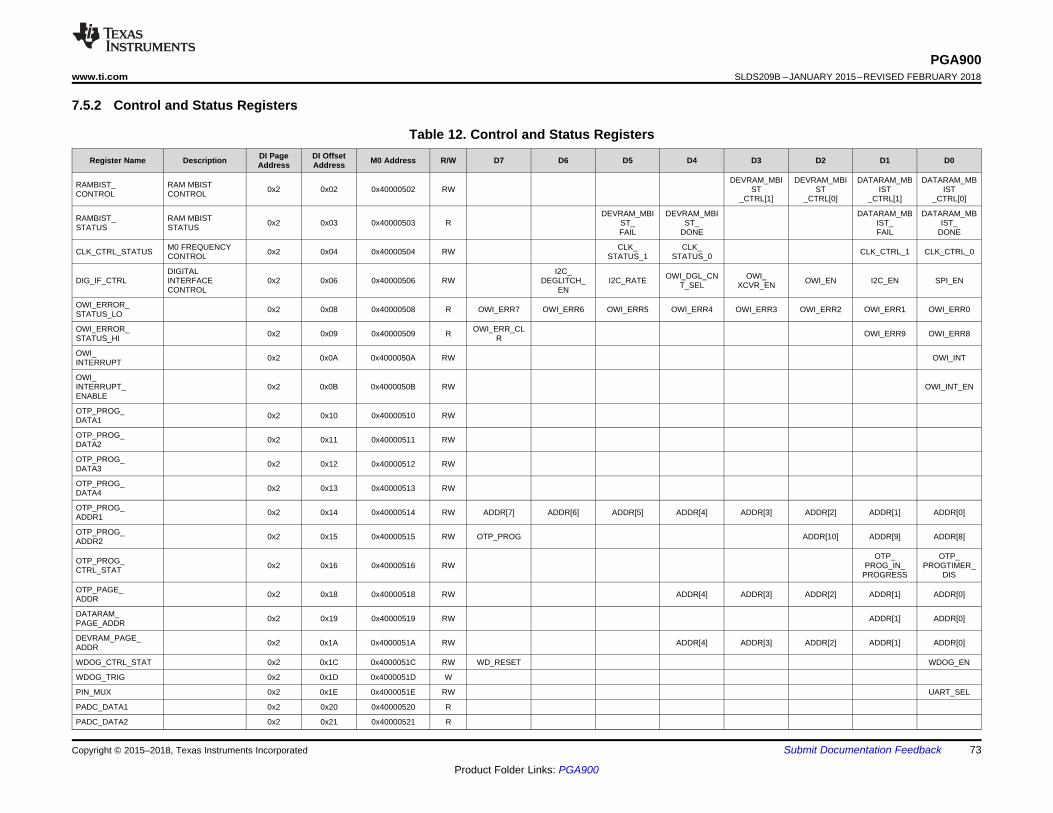
PGA900www.ti.com SLDS209B –JANUARY 2015–REVISED FEBRUARY 2018
73
Product Folder Links: PGA900
Submit Documentation FeedbackCopyright © 2015–2018, Texas Instruments Incorporated
7.5.2 Control and Status Registers
Table 12. Control and Status Registers
Register Name Description DI PageAddress
DI OffsetAddress M0 Address R/W D7 D6 D5 D4 D3 D2 D1 D0
RAMBIST_CONTROL
RAM MBISTCONTROL 0x2 0x02 0x40000502 RW
DEVRAM_MBIST
_CTRL[1]
DEVRAM_MBIST
_CTRL[0]
DATARAM_MBIST
_CTRL[1]
DATARAM_MBIST
_CTRL[0]
RAMBIST_STATUS
RAM MBISTSTATUS 0x2 0x03 0x40000503 R
DEVRAM_MBIST_FAIL
DEVRAM_MBIST_
DONE
DATARAM_MBIST_FAIL
DATARAM_MBIST_
DONE
CLK_CTRL_STATUS M0 FREQUENCYCONTROL 0x2 0x04 0x40000504 RW CLK_
STATUS_1CLK_
STATUS_0 CLK_CTRL_1 CLK_CTRL_0
DIG_IF_CTRLDIGITALINTERFACECONTROL
0x2 0x06 0x40000506 RWI2C_
DEGLITCH_EN
I2C_RATE OWI_DGL_CNT_SEL
OWI_XCVR_EN OWI_EN I2C_EN SPI_EN
OWI_ERROR_STATUS_LO 0x2 0x08 0x40000508 R OWI_ERR7 OWI_ERR6 OWI_ERR5 OWI_ERR4 OWI_ERR3 OWI_ERR2 OWI_ERR1 OWI_ERR0
OWI_ERROR_STATUS_HI 0x2 0x09 0x40000509 R OWI_ERR_CL
R OWI_ERR9 OWI_ERR8
OWI_INTERRUPT 0x2 0x0A 0x4000050A RW OWI_INT
OWI_INTERRUPT_ENABLE
0x2 0x0B 0x4000050B RW OWI_INT_EN
OTP_PROG_DATA1 0x2 0x10 0x40000510 RW
OTP_PROG_DATA2 0x2 0x11 0x40000511 RW
OTP_PROG_DATA3 0x2 0x12 0x40000512 RW
OTP_PROG_DATA4 0x2 0x13 0x40000513 RW
OTP_PROG_ADDR1 0x2 0x14 0x40000514 RW ADDR[7] ADDR[6] ADDR[5] ADDR[4] ADDR[3] ADDR[2] ADDR[1] ADDR[0]
OTP_PROG_ADDR2 0x2 0x15 0x40000515 RW OTP_PROG ADDR[10] ADDR[9] ADDR[8]
OTP_PROG_CTRL_STAT 0x2 0x16 0x40000516 RW
OTP_PROG_IN_
PROGRESS
OTP_PROGTIMER_
DIS
OTP_PAGE_ADDR 0x2 0x18 0x40000518 RW ADDR[4] ADDR[3] ADDR[2] ADDR[1] ADDR[0]
DATARAM_PAGE_ADDR 0x2 0x19 0x40000519 RW ADDR[1] ADDR[0]
DEVRAM_PAGE_ADDR 0x2 0x1A 0x4000051A RW ADDR[4] ADDR[3] ADDR[2] ADDR[1] ADDR[0]
WDOG_CTRL_STAT 0x2 0x1C 0x4000051C RW WD_RESET WDOG_EN
WDOG_TRIG 0x2 0x1D 0x4000051D W
PIN_MUX 0x2 0x1E 0x4000051E RW UART_SEL
PADC_DATA1 0x2 0x20 0x40000520 R
PADC_DATA2 0x2 0x21 0x40000521 R

PGA900SLDS209B –JANUARY 2015–REVISED FEBRUARY 2018 www.ti.com
74
Product Folder Links: PGA900
Submit Documentation Feedback Copyright © 2015–2018, Texas Instruments Incorporated
Table 12. Control and Status Registers (continued)Register Name Description DI Page
AddressDI OffsetAddress M0 Address R/W D7 D6 D5 D4 D3 D2 D1 D0
PADC_DATA3 0x2 0x22 0x40000522 R
PADC_CONFIG 0x2 0x23 0x40000523 RW PADC_INT_RATE
PADC_DECI_RATE
PADC_EN_24BIT PADC_EN
TADC_DATA1 0x2 0x24 0x40000524 R
TADC_DATA2 0x2 0x25 0x40000525 R
TADC_DATA3 0x2 0x26 0x40000526 R
TADC_CONFIG 0x2 0x27 0x40000527 RW TADC_INT_RATE
TADC_DECI_RATE
TADC_EN_24BIT TADC_EN
ADC_CFG_1 0x2 0x29 0x40000529 RW Write 0 Write 0 ADC_EN Write 0 Write 0 RESET_CLK
RESET_MOD
DAC_REG0_1 0x2 0x30 0x40000530 RW
DAC_REG0_2 0x2 0x31 0x40000531 RW
DAC_REG1_1 0x2 0x32 0x40000532 RW
DAC_REG1_2 0x2 0x33 0x40000533 RW
DAC_CTRL_STATUS 0x2 0x38 0x40000538 RW DAC_
ENABLE
DAC_CONFIG 0x2 0x39 0x40000539 RW DAC_RATIOMETRIC
DAC_LPBK_CTRL 0x2 0x3A 0x4000053A RW EN_LB LB_AMP_
ENLB_
CONNECT
OP_STAGE_CTRL 0x2 0x3B 0x4000053B RW PULLUP_EN DACCAP_EN 4_20MA_EN DAC_GAIN[2] DAC_GAIN[1] DAC_GAIN[0]
AFE_CFG 0x0 0xF4 0x400004F4 RW Write 0 Write 0 PGAIN_OPEN Write 0 Write 0 Write 0 Write 0 Write 0
AFEDIAG_CFG 0x2 0x45 0x40000545 RW DIS_R_TEMP DIS_R_SD FAULT_THRS[2]
FAULT_THRS[1]
FAULT_THRS[0] DIS_R2M DIS_R1M
BRDG_CTRL 0x2 0x46 0x40000546 RW VBRDG_CTRL[1]
VBRDG_CTRL[0] BRDG_EN
P_GAIN_SELECT 0x2 0x47 0x40000547 RW P_INV P_GAIN[4] P_GAIN[3] P_GAIN[2] P_GAIN[1] P_GAIN[0]
T_GAIN_SELECT 0x2 0x48 0x40000548 RW T_INV T_GAIN[1] T_GAIN[0]
TEMP_CTRL 0x2 0x4C 0x4000054C RW ITEMP_CTRL[2]
ITEMP_CTRL[1]
ITEMP_CTRL[0]
TEMP_MUX_CTRL[3]
TEMP_MUX_CTRL[2]
TEMP_MUX_CTRL[1]
TEMP_MUX_CTRL[0]
ALPWR 0x2 0x50 0x40000550 GATE_CTRL_SD
ADC_EN_VREF SD
DLPWR 0x2 0x54 0x40000554 RW OWI_CLK_EN
PSMON1 0x2 0x58 0x40000558 RW OSC_VDD_UV OSC_VDD_OV AVDD_UV AVDD_OV REF_UV REF_OV VBRG_UV VBRG_OV
PSMON2 0x2 0x59 0x40000559 RW DVDD_UV DVDD_OV
AFEDIAG 0x2 0x5A 0x4000055A RW TGAIN_UV TGAIN_OV PGAIN_UV PGAIN_OV VINT_OV VINP_UV VINP_OV
TOPDIG_MUX_SEL 0x2 0x60 0x40000560 RW TOPDIG[5] TOPDIG[4] TOPDIG[3] TOPDIG[2] TOPDIG[1] TOPDIG[0]
TONDIG_MUX_SEL 0x2 0x61 0x40000561 RW TONDIG[5] TONDIG[4] TONDIG[3] TONDIG[2] TONDIG[1] TONDIG[0]
AMUX_ACT 0x2 0x64 0x40000564 RW TOUT_MUX_SEL TIN_MUX_EN

PGA900www.ti.com SLDS209B –JANUARY 2015–REVISED FEBRUARY 2018
75
Product Folder Links: PGA900
Submit Documentation FeedbackCopyright © 2015–2018, Texas Instruments Incorporated
Table 12. Control and Status Registers (continued)Register Name Description DI Page
AddressDI OffsetAddress M0 Address R/W D7 D6 D5 D4 D3 D2 D1 D0
AMUX_TIN_MUX_CTRL 0x2 0x65 0x40000565 RW
AMUX_TIN_MUX_CTRL
[2]
AMUX_TIN_MUX_CTRL
[1]
AMUX_TIN_MUX_CTRL[0]
AMUX_TOUT_MUX_CTRL 0x2 0x66 0x40000566 RW
AMUX_TOUT_MUX_CTRL
[3]
AMUX_TOUT_MUX_CTRL [2]
AMUX_TOUT_MUX_CTRL
[1]
AMUX_TOUT_MUX_CTRL
[0]
AMUX_CTRL 0x2 0x67 0x40000567 RW TSEM_NTEST_
MUX_T_EN
TEST_MUX_P_
EN
TEST_MUX_DAC_
EN
TRACE_FIFO_CTRL_STAT 0x2 0x70 0x40000570 RW
TRACE_FIFO_FULL
TRACE_FIFO_HALF_FULL
TRACE_FIFO_
EMPTY
TRACE_SOURCE
TRACE_FIFO_
ENABLE
REVISION_ID1 0x0 0x00 0x40000400 R OPT_ID[2] OPT_ID[1] OPT_ID[0] REV_ID[3] REV_ID[2] REV_ID[1] REV_ID[0]
REVISION_ID2 0x0 0x01 0x40000401 R DL_ID[3] DL_ID[2] DL_ID[1] DL_ID[0]
COM_MCU_TO_DIF_B1 0x0 0x04 0x40000404 RW
COM_MCU_TO_DIF_B2 0x0 0x05 0x40000405 RW
COM_TX_STATUS 0x0 0x06 0x40000406 RW COM_TXRDY
COM_DIF_TO_MCU_B1 0x0 0x08 0x40000408 RW
COM_DIF_TO_MCU_B2 0x0 0x09 0x40000409 RW
COM_RX_STATUS 0x0 0x0A 0x4000040A RW COM_RXRDY
COM_RX_INT_ENABLE 0x0 0x0B 0x4000040B RW COM_RXRDY_
INT_EN
MICRO_INTERFACE_CONTROL
0x0 0x0C 0x4000040C RW DEBUG_LOCK MICRO_RESET IF_SEL
SECLOCK 0x0 0x0D 0x4000040D RW SECLOCK
UART_CONFIG 0x7 0x00 0x40000200 RW TWO_STOP_BITS PARITY PARITY_EN
UART_EN 0x7 0x01 0x40000201 RW UART_EN
BAUD_RATE_LO 0x7 0x02 0x40000202 RW
BAUD_RATE_HI 0x7 0x03 0x40000203 RW
UART_LINE_STATUS 0x7 0x04 0x40000204 RW TX_COMPLET
E RX_READY FRAMING_ERROR
PARITY_ERROR
OVERRUN_ERROR
UART_INTERRUPT_STATUS 0x7 0x08 0x40000208 R
UART_TXCOMPLETE
_I
UART_RXRDY_I
UART_INTERRUPT_ENABLE 0x7 0x0A 0x4000020A RW
UART_TXCOMPLET_
INT_EN
UART_RXRDY_INT_EN
UART_RX_BUF 0x7 0x0C 0x4000020C R
UART_TX_BUF 0x7 0x0E 0x4000020E RW
PWM_ON_TIME1 0x7 0x10 0x40000210 RW
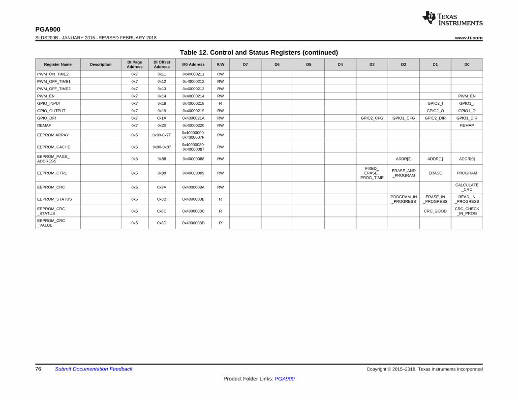
PGA900SLDS209B –JANUARY 2015–REVISED FEBRUARY 2018 www.ti.com
76
Product Folder Links: PGA900
Submit Documentation Feedback Copyright © 2015–2018, Texas Instruments Incorporated
Table 12. Control and Status Registers (continued)Register Name Description DI Page
AddressDI OffsetAddress M0 Address R/W D7 D6 D5 D4 D3 D2 D1 D0
PWM_ON_TIME2 0x7 0x11 0x40000211 RW
PWM_OFF_TIME1 0x7 0x12 0x40000212 RW
PWM_OFF_TIME2 0x7 0x13 0x40000213 RW
PWM_EN 0x7 0x14 0x40000214 RW PWM_EN
GPIO_INPUT 0x7 0x18 0x40000218 R GPIO2_I GPIO1_I
GPIO_OUTPUT 0x7 0x19 0x40000219 RW GPIO2_O GPIO1_O
GPIO_DIR 0x7 0x1A 0x4000021A RW GPIO2_CFG GPIO1_CFG GPIO2_DIR GPIO1_DIR
REMAP 0x7 0x20 0x40000220 RW REMAP
EEPROM ARRAY 0x5 0x00-0x7F 0x40000000-0x4000007F RW
EEPROM_CACHE 0x5 0x80-0x87 0x40000080-0x40000087 RW
EEPROM_PAGE_ADDRESS 0x5 0x88 0x40000088 RW ADDR[2] ADDR[1] ADDR[0]
EEPROM_CTRL 0x5 0x89 0x40000089 RWFIXED_ERASE_
PROG_TIME
ERASE_AND_PROGRAM ERASE PROGRAM
EEPROM_CRC 0x5 0x8A 0x4000008A RW CALCULATE_CRC
EEPROM_STATUS 0x5 0x8B 0x4000008B R PROGRAM_IN_PROGRESS
ERASE_IN_PROGRESS
READ_IN_PROGRESS
EEPROM_CRC_STATUS 0x5 0x8C 0x4000008C R CRC_GOOD CRC_CHECK
_IN_PROG
EEPROM_CRC_VALUE 0x5 0x8D 0x4000008D R

77
PGA900www.ti.com SLDS209B –JANUARY 2015–REVISED FEBRUARY 2018
Product Folder Links: PGA900
Submit Documentation FeedbackCopyright © 2015–2018, Texas Instruments Incorporated
Table 13. Cortex M0 Specific RegistersRegister Name Description M0 Address
SYST_CSR SysTick Control and Status Register 0xE000E010SYST_RVR SysTick Reload Value Register 0xE000E014SYST_CVR SysTick Current Value Register 0xE000E018ISER Interrupt Set-Enable Register 0xE000E100ICER Interrupt Clear-Enable Register 0xE000E180ISPR Interrupt Set-Pending Register 0xE000E200ICPR Interrupt Clear-Pending Register 0xE000E280IPR Interrupt Priority Registers 0xE000E400-0xE000E41C
SPACE
NOTEFor details of the Cortex M0 specific registers, refer to ARM_M0_User_guide.pdf that canbe downloaded from the ARM website (www.arm.com).
7.5.2.1 RAM MBIST Control (M0 address = 0x40000502) (DI page address = 0x2) (DI page offset = 0x02)
Figure 50. RAMBIST_CONTROL
7 6 5 4 3 2 1 0DEVRAM_MBI
ST_CTRL[1]
DEVRAM_MBIST
_CTRL[0]
DATARAM_MBIST
_CTRL[1]
DATARAM_MBIST
_CTRL[0]RW RW RW RW0 0 0 0
Table 14. RAMBIST_CONTROL Field DescriptionsBit
Definitions Bit
RAMBIST_CONTROL
0:DATARAM_MBIST_CTRL[0]
DATARAM_MBIST_CTRL[1] DATARAM_MBIST_CTRL[0]
0 0 DATARAM MBIST is inactive
1:DATARAM_MBIST_CTRL[1]
0 1 Invalid1 0 Invalid1 1 DATARAM MBIST is active
2:DEVRAM_MBIST_CTRL[0]
DEVRAM_MBIST_CTRL[1] DEVRAM_MBIST_CTRL[0]0 0 DEVRAM MBIST is inactive0 1 Invalid
3:DEVRAM_MBIST_CTRL[1]
1 0 Invalid
1 1 DEVRAM MBIST is active
4:5:6:7:
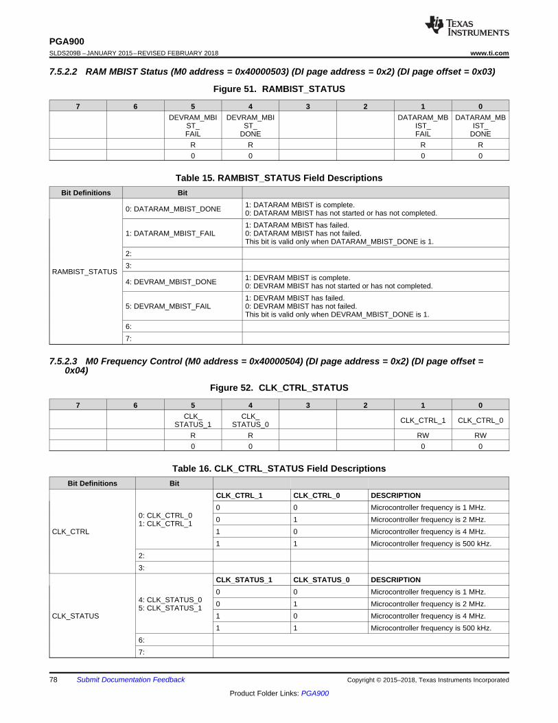
78
PGA900SLDS209B –JANUARY 2015–REVISED FEBRUARY 2018 www.ti.com
Product Folder Links: PGA900
Submit Documentation Feedback Copyright © 2015–2018, Texas Instruments Incorporated
7.5.2.2 RAM MBIST Status (M0 address = 0x40000503) (DI page address = 0x2) (DI page offset = 0x03)
Figure 51. RAMBIST_STATUS
7 6 5 4 3 2 1 0DEVRAM_MBI
ST_FAIL
DEVRAM_MBIST_
DONE
DATARAM_MBIST_FAIL
DATARAM_MBIST_
DONER R R R0 0 0 0
Table 15. RAMBIST_STATUS Field DescriptionsBit Definitions Bit
RAMBIST_STATUS
0: DATARAM_MBIST_DONE 1: DATARAM MBIST is complete.0: DATARAM MBIST has not started or has not completed.
1: DATARAM_MBIST_FAIL1: DATARAM MBIST has failed.0: DATARAM MBIST has not failed.This bit is valid only when DATARAM_MBIST_DONE is 1.
2:3:
4: DEVRAM_MBIST_DONE 1: DEVRAM MBIST is complete.0: DEVRAM MBIST has not started or has not completed.
5: DEVRAM_MBIST_FAIL1: DEVRAM MBIST has failed.0: DEVRAM MBIST has not failed.This bit is valid only when DEVRAM_MBIST_DONE is 1.
6:7:
7.5.2.3 M0 Frequency Control (M0 address = 0x40000504) (DI page address = 0x2) (DI page offset =0x04)
Figure 52. CLK_CTRL_STATUS
7 6 5 4 3 2 1 0CLK_
STATUS_1CLK_
STATUS_0 CLK_CTRL_1 CLK_CTRL_0
R R RW RW0 0 0 0
Table 16. CLK_CTRL_STATUS Field DescriptionsBit Definitions Bit
CLK_CTRL
0: CLK_CTRL_01: CLK_CTRL_1
CLK_CTRL_1 CLK_CTRL_0 DESCRIPTION0 0 Microcontroller frequency is 1 MHz.0 1 Microcontroller frequency is 2 MHz.1 0 Microcontroller frequency is 4 MHz.1 1 Microcontroller frequency is 500 kHz.
2:3:
CLK_STATUS
4: CLK_STATUS_05: CLK_STATUS_1
CLK_STATUS_1 CLK_STATUS_0 DESCRIPTION0 0 Microcontroller frequency is 1 MHz.0 1 Microcontroller frequency is 2 MHz.1 0 Microcontroller frequency is 4 MHz.1 1 Microcontroller frequency is 500 kHz.
6:7:
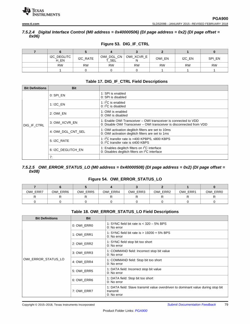
79
PGA900www.ti.com SLDS209B –JANUARY 2015–REVISED FEBRUARY 2018
Product Folder Links: PGA900
Submit Documentation FeedbackCopyright © 2015–2018, Texas Instruments Incorporated
7.5.2.4 Digital Interface Control (M0 address = 0x40000506) (DI page address = 0x2) (DI page offset =0x06)
Figure 53. DIG_IF_CTRL
7 6 5 4 3 2 1 0I2C_DEGLITC
H_EN I2C_RATE OWI_DGL_CNT_SEL
OWI_XCVR_EN OWI_EN I2C_EN SPI_EN
RW RW RW RW RW RW RW1 0 0 0 1 1 1
Table 17. DIG_IF_CTRL Field DescriptionsBit Definitions Bit
DIG_IF_CTRL
0: SPI_EN 1: SPI is enabled0: SPI is disabled
1: I2C_EN 1: I2C is enabled0: I2C is disabled
2: OWI_EN 1: OWI is enabled0: OWI is disabled
3: OWI_XCVR_EN 1: Enable OWI Transceiver – OWI transceiver is connected to VDD0: Disable OWI Transceiver – OWI transceiver is disconnected from VDD
4: OWI_DGL_CNT_SEL 1: OWI activation deglitch filters are set to 10ms0: OWI activation deglitch filters are set to 1ms
5: I2C_RATE 1: I2C transfer rate is >400 KPBPS, ≤800 KBPS0: I2C transfer rate is ≤400 KBPS
6: I2C_DEGLITCH_EN 1: Enables deglitch filters on I2C interface0: Disables deglitch filters on I2C interface
7:
7.5.2.5 OWI_ERROR_STATUS_LO (M0 address = 0x40000508) (DI page address = 0x2) (DI page offset =0x08)
Figure 54. OWI_ERROR_STATUS_LO
7 6 5 4 3 2 1 0OWI_ERR7 OWI_ERR6 OWI_ERR5 OWI_ERR4 OWI_ERR3 OWI_ERR2 OWI_ERR1 OWI_ERR0
R R R R R R R R0 0 0 0 0 0 0 0
Table 18. OWI_ERROR_STATUS_LO Field DescriptionsBit Definitions Bit
OWI_ERROR_STATUS_LO
0: OWI_ERR0 1: SYNC field bit rate is < 320 – 5% BPS0: No error
1: OWI_ERR1 1: SYNC field bit rate is > 19200 + 5% BPS0: No error
2: OWI_ERR2 1: SYNC field stop bit too short0: No error
3: OWI_ERR3 1: COMMAND field: Incorrect stop bit value0: No error
4: OWI_ERR4 1: COMMAND field: Stop bit too short0: No error
5: OWI_ERR5 1: DATA field: Incorrect stop bit value0: No error
6: OWI_ERR6 1: DATA field: Stop bit too short0: No error
7: OWI_ERR71: DATA field: Slave transmit value overdriven to dominant value during stop bittransmit0: No error

80
PGA900SLDS209B –JANUARY 2015–REVISED FEBRUARY 2018 www.ti.com
Product Folder Links: PGA900
Submit Documentation Feedback Copyright © 2015–2018, Texas Instruments Incorporated
7.5.2.6 OWI_ERROR_STATUS_HI (M0 address = 0x40000509) (DI page address = 0x2) (DI page offset =0x09)
Figure 55. OWI_ERROR_STATUS_HI
7 6 5 4 3 2 1 0OWI_ERR_CL
R OWI_ERR9 OWI_ERR8
RW R R0 0 0
Table 19. OWI_ERROR_STATUS_HI Field DescriptionsBit Definitions Bit
OWI_ERROR_STATUS_HI
0: OWI_ERR81: SYNC field: Consecutive bits in the sync field are different by more than ±19%tolerance0: No error
1: OWI_ERR9 1: COMMAND field: Invalid command sent through OWI protocol0: No error
2:3:4:5:6:
7: OWI_ERR_CLR 1: Clear OWI_ERROR_STATUS_LO and OWI_ERROR_STATUS_HI registers0: No action
7.5.2.7 OWI_INTERRUPT (M0 address = 0x4000050A) (DI page address = 0x2) (DI page offset = 0x0A)
Figure 56. OWI_INTERRUPT
7 6 5 4 3 2 1 0OWI_INT
RW0
Table 20. OWI_INTERRUPT Field DescriptionsBit Definitions Bit
OWI_INTERRUPT
0: OWI_INTRead Write1: OWI interrupt is active0: No action
1: Clear OWI interrupt0: No action
1:2:3:4:5:6:7:

81
PGA900www.ti.com SLDS209B –JANUARY 2015–REVISED FEBRUARY 2018
Product Folder Links: PGA900
Submit Documentation FeedbackCopyright © 2015–2018, Texas Instruments Incorporated
7.5.2.8 OWI_INTERRUPT_EN (M0 address = 0x4000050B) (DI page address = 0x2) (DI page offset = 0x0B)
Figure 57. OWI_INTERRUPT_EN
7 6 5 4 3 2 1 0OWI_INT_EN
RW0
Table 21. OWI_INTERRUPT_EN Field DescriptionsBit Definitions Bit
OWI_INTERRUPT_EN
0: OWI_INT_EN 1: Enable OWI interrupt0: No error
1:2:3:4:5:6:7:
7.5.2.9 OTP_PROG_DATA1-4
Figure 58. OTP_PROG_DATA1 (M0 address = 0x40000510) (DI page address = 0x2) (DI page offset =0x10)
7 6 5 4 3 2 1 0
RW RW RW RW RW RW RW RW0 0 0 0 0 0 0 0
Figure 59. OTP_PROG_DATA2 (M0 address = 0x40000511) (DI page address = 0x2) (DI page offset =0x11)
7 6 5 4 3 2 1 0
RW RW RW RW RW RW RW RW0 0 0 0 0 0 0 0
Figure 60. OTP_PROG_DATA3 (M0 address = 0x40000512) (DI page address = 0x2) (DI page offset =0x12)
7 6 5 4 3 2 1 0
RW RW RW RW RW RW RW RW0 0 0 0 0 0 0 0
Figure 61. OTP_PROG_DATA4 (M0 address = 0x40000513) (DI page address = 0x2) (DI page offset =0x13)
7 6 5 4 3 2 1 0
RW RW RW RW RW RW RW RW0 0 0 0 0 0 0 0
Little-endian mode.

82
PGA900SLDS209B –JANUARY 2015–REVISED FEBRUARY 2018 www.ti.com
Product Folder Links: PGA900
Submit Documentation Feedback Copyright © 2015–2018, Texas Instruments Incorporated
7.5.2.10 OTP_PROG_ADDR1-2
Figure 62. OTP_PROG_ADDR1 (M0 address = 0x40000514) (DI page address = 0x2) (DI page offset =0x14)
7 6 5 4 3 2 1 0ADDR[7] ADDR[6] ADDR[5] ADDR[4] ADDR[3] ADDR[2] ADDR[1] ADDR[0]
RW RW RW RW RW RW RW RW0 0 0 0 0 0 0 0
Figure 63. OTP_PROG_ADDR2 (M0 address = 0x40000515) (DI page address = 0x2) (DI page offset =0x15)
7 6 5 4 3 2 1 0OTP_PROG ADDR[10] ADDR[9] ADDR[8]
RW RW RW RW0 0 0 0
Table 22. OTP_PROG_ADDR1-2 Field DescriptionsBit Definitions Bit
OTP_PROG_ADDR2
0: ADDR[8]1: ADDR[9]2: ADDR[10]3:4:5:6:
7: OTP_PROG
1: The data is programmed specified by OTP_PROG_DATA1-4 is programmed intoaddress specified by bits OTP_PROG_ADDR bits [10:0]. The bit is automaticallycleared when the internal program timer in the OTP controller is used when theprogramming starts. The bit retains the state until cleared by software when theprogram timer in the OTP controller is disabled0: No action

83
PGA900www.ti.com SLDS209B –JANUARY 2015–REVISED FEBRUARY 2018
Product Folder Links: PGA900
Submit Documentation FeedbackCopyright © 2015–2018, Texas Instruments Incorporated
7.5.2.11 OTP_PROG_CTRL_STAT (M0 address = 0x40000516) (DI page address = 0x2) (DI page offset =0x16)
Figure 64. OTP_PROG_CTRL_STAT
7 6 5 4 3 2 1 0OTP_
PROG_IN_PROGRESS
OTP_PROGTIMER_
DISR RW0 0
Table 23. OTP_PROG_CTRL_STAT Field DescriptionsBit Definitions Bit
OTP_PROG_CTRL_STAT
0: OTP_PROGTIMER_DIS
1: OTP programming timer is disabled. When the program timer isdisabled, the program timing is controlled by assertion and de-assertion of the OTP_PROG bit in the OTP_PROG_ADDR register0: OTP programming timer is enabled.
1: OTP_PROG_IN_PROGRESS1: Indicates that the programming is in progress. This bit is valid onlywhen the OTP_PROGTIMER_DIS is 0.0: N/A
2:3:4:5:6:7:
7.5.2.12 OTP_PAGE_ADDR (M0 address = 0x40000518) (DI page address = 0x2) (DI page offset = 0x18)
Figure 65. OTP_PAGE_ADDR
7 6 5 4 3 2 1 0ADDR[4] ADDR[3] ADDR[2] ADDR[1] ADDR[0]
RW RW RW RW RW0 0 0 0 0
7.5.2.13 DATARAM_PAGE_ADDR (M0 address = 0x40000519) (DI page address = 0x2) (DI page offset =0x19)
Figure 66. DATARAM_PAGE_ADDR
7 6 5 4 3 2 1 0ADDR[1] ADDR[0]
RW RW0 0
7.5.2.14 DEVRAM_PAGE_ADDR (M0 address = 0x4000051A) (DI page address = 0x2) (DI page offset =0x1A)
Figure 67. DEVRAM_PAGE_ADDR
7 6 5 4 3 2 1 0ADDR[4] ADDR[3] ADDR[2] ADDR[1] ADDR[0]
RW RW RW RW RW0 0 0 0 0

84
PGA900SLDS209B –JANUARY 2015–REVISED FEBRUARY 2018 www.ti.com
Product Folder Links: PGA900
Submit Documentation Feedback Copyright © 2015–2018, Texas Instruments Incorporated
7.5.2.15 WDOG_CTRL_STAT (M0 address = 0x4000051C) (DI page address = 0x2) (DI page offset = 0x1C)
Figure 68. WDOG_CTRL_STAT
7 6 5 4 3 2 1 0WD_RESET WDOG_EN
RW RW0 0
Table 24. WDOG_CTRL_STAT Field DescriptionsBit Definitions Bit
WDOG_CTRL_STAT
0: WDOG_EN 1:Watchdog timer is enabled0: Watchdog timer is disabled
1:2:3:4:5:6:
7: WD_RESET 1: Watchdog timer is timed out. This bit is cleared when 1 is written to it.0: N/A
7.5.2.16 WDOG_TRIG (M0 address = 0x4000051D) (DI page address = 0x2) (DI page offset = 0x1D)
Figure 69. WDOG_TRIG
7 6 5 4 3 2 1 0
RW RW RW RW RW RW RW RW1 1 1 1 1 1 1 1
• Writing any 8-bit value to this register, resets the watchdog timer.• The watchdog timeout value is (WDOG_TRIG + 1) × 2 ms.
7.5.2.17 PIN_MUX (M0 address = 0x4000051E) (DI page address = 0x2) (DI page offset = 0x1E)
Figure 70. PIN_MUX
7 6 5 4 3 2 1 0UART_SEL
RW0
Table 25. PIN_MUX Field DescriptionsBit Definitions Bit
PIN_MUX
0: UART_SEL 1: MOSI/RX and MISO/TX pins are configured for UART0: MOSI/RX and MISO/TX pins are configured for SPI
1:2:3:4:5:6:7:
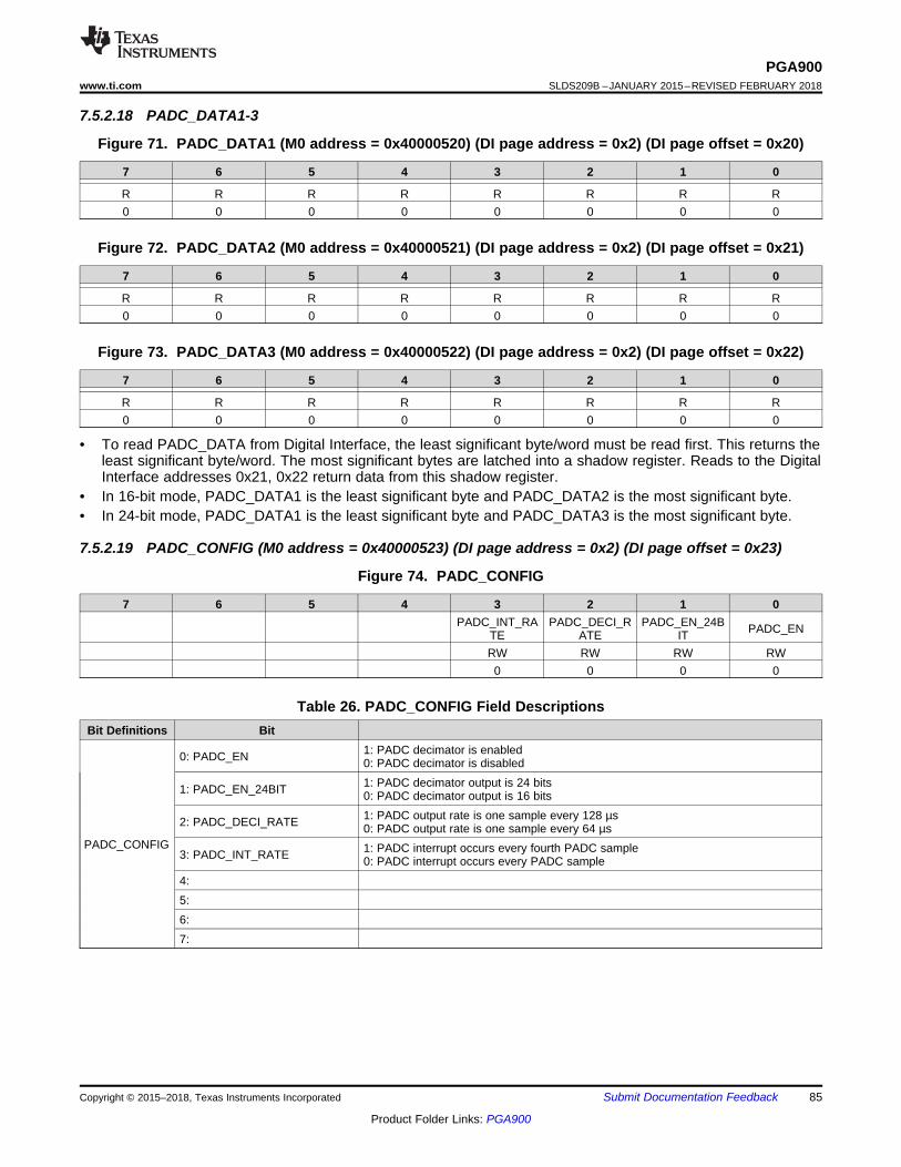
85
PGA900www.ti.com SLDS209B –JANUARY 2015–REVISED FEBRUARY 2018
Product Folder Links: PGA900
Submit Documentation FeedbackCopyright © 2015–2018, Texas Instruments Incorporated
7.5.2.18 PADC_DATA1-3
Figure 71. PADC_DATA1 (M0 address = 0x40000520) (DI page address = 0x2) (DI page offset = 0x20)
7 6 5 4 3 2 1 0
R R R R R R R R0 0 0 0 0 0 0 0
Figure 72. PADC_DATA2 (M0 address = 0x40000521) (DI page address = 0x2) (DI page offset = 0x21)
7 6 5 4 3 2 1 0
R R R R R R R R0 0 0 0 0 0 0 0
Figure 73. PADC_DATA3 (M0 address = 0x40000522) (DI page address = 0x2) (DI page offset = 0x22)
7 6 5 4 3 2 1 0
R R R R R R R R0 0 0 0 0 0 0 0
• To read PADC_DATA from Digital Interface, the least significant byte/word must be read first. This returns theleast significant byte/word. The most significant bytes are latched into a shadow register. Reads to the DigitalInterface addresses 0x21, 0x22 return data from this shadow register.
• In 16-bit mode, PADC_DATA1 is the least significant byte and PADC_DATA2 is the most significant byte.• In 24-bit mode, PADC_DATA1 is the least significant byte and PADC_DATA3 is the most significant byte.
7.5.2.19 PADC_CONFIG (M0 address = 0x40000523) (DI page address = 0x2) (DI page offset = 0x23)
Figure 74. PADC_CONFIG
7 6 5 4 3 2 1 0PADC_INT_RA
TEPADC_DECI_R
ATEPADC_EN_24B
IT PADC_EN
RW RW RW RW0 0 0 0
Table 26. PADC_CONFIG Field DescriptionsBit Definitions Bit
PADC_CONFIG
0: PADC_EN 1: PADC decimator is enabled0: PADC decimator is disabled
1: PADC_EN_24BIT 1: PADC decimator output is 24 bits0: PADC decimator output is 16 bits
2: PADC_DECI_RATE 1: PADC output rate is one sample every 128 µs0: PADC output rate is one sample every 64 µs
3: PADC_INT_RATE 1: PADC interrupt occurs every fourth PADC sample0: PADC interrupt occurs every PADC sample
4:5:6:7:

86
PGA900SLDS209B –JANUARY 2015–REVISED FEBRUARY 2018 www.ti.com
Product Folder Links: PGA900
Submit Documentation Feedback Copyright © 2015–2018, Texas Instruments Incorporated
7.5.2.20 TADC_DATA1-3
Figure 75. TADC_DATA1 (M0 address = 0x40000524) (DI page address = 0x2) (DI page offset = 0x24)
7 6 5 4 3 2 1 0
R R R R R R R R0 0 0 0 0 0 0 0
Figure 76. TADC_DATA2 (M0 address = 0x40000525) (DI page address = 0x2) (DI page offset = 0x25)
7 6 5 4 3 2 1 0
R R R R R R R R0 0 0 0 0 0 0 0
Figure 77. TADC_DATA3 (M0 address = 0x40000526) (DI page address = 0x2) (DI page offset = 0x26)
7 6 5 4 3 2 1 0
R R R R R R R R0 0 0 0 0 0 0 0
• To read TADC_DATA from Digital Interface, the least significant byte/word must be read first. This returns theleast significant byte/word. The most significant bytes are latched into a shadow register. Reads to the DigitalInterface addresses 0x25, 0x26 return data from this shadow register.
• In 16-bit mode, TADC_DATA1 is the least significant byte and TADC_DATA2 is the most significant byte.• In 24-bit mode, TADC_DATA1 is the least significant byte and TADC_DATA3 is the most significant byte.
7.5.2.21 TADC_CONFIG (M0 address = 0x40000527) (DI page address = 0x2) (DI page offset = 0x27)
Figure 78. TADC_CONFIG
7 6 5 4 3 2 1 0TADC_INT_RA
TETADC_DECI_R
ATETADC_EN_24B
IT TADC_EN
RW RW RW RW0 0 0 0
Table 27. TADC_CONFIG Field DescriptionsBit Definitions Bit
TADC_CONFIG
0: TADC_EN 1: TADC decimator is enabled0: TADC decimator is disabled
1: TADC_EN_24BIT 1: TADC decimator output is 24 bits0: TADC decimator output is 16 bits
2: TADC_DECI_RATE 1: TADC output rate is one sample every 128 µs0: TADC output rate is one sample every 64 µs
3: TADC_INT_RATE 1: TADC interrupt occurs every fourth TADC sample0: TADC interrupt occurs every TADC sample
4:5:6:7:

87
PGA900www.ti.com SLDS209B –JANUARY 2015–REVISED FEBRUARY 2018
Product Folder Links: PGA900
Submit Documentation FeedbackCopyright © 2015–2018, Texas Instruments Incorporated
7.5.2.22 ADC_CFG_1 (M0 address = 0x40000529) (DI page address = 0x2) (DI page offset = 0x29)
Figure 79. ADC_CFG_1
7 6 5 4 3 2 1 0Write 0 Write 0 ADC_EN Write 0 Write 0 RESET_CLK RESET_MOD
RW RW RW RW RW RW RW0 0 0 0 0 1 1
Table 28. ADC_CFG_1 Field DescriptionsBit Definitions Bit
ADC_CFG_1
0: RESET_MOD 1: PADC and TADC sigma-delta modulators are in reset0: PADC and TADC sigma-delta modulators are not in reset
1: RESET_CLK 1: PADC and TADC sigma-delta modulators clocks are reset0: PADC and TADC sigma-delta modulators clocks are not in reset
2: Always write 03: Always write 0
4: ADC_EN 1: ADC interfaces and decimator clocks are enabled0: ADC interfaces and decimator clocks are disabled
5: Always write 06: Always write 07:
7.5.2.23 DAC_REG
Figure 80. DAC_REG0_1 (M0 address = 0x40000530) (DI page address = 0x2) (DI page offset = 0x30)
7 6 5 4 3 2 1 0
RW RW RW RW RW RW RW RW0 0 0 0 0 0 0 0
Figure 81. DAC_REG0_2 (M0 address = 0x40000531) (DI page address = 0x2) (DI page offset = 0x31)
7 6 5 4 3 2 1 0
RW RW RW RW RW RW RW RW0 0 0 0 0 0 0 0
Figure 82. DAC_REG1_1 (M0 address = 0x40000532) (DI page address = 0x2) (DI page offset = 0x32)
7 6 5 4 3 2 1 0
RW RW RW RW RW RW RW RW0 0 0 0 0 0 0 0
Figure 83. DAC_REG1_2 (M0 address = 0x40000533) (DI page address = 0x2) (DI page offset = 0x33)
7 6 5 4 3 2 1 0
RW RW RW RW RW RW RW RW0 0 0 0 0 0 0 0
DAC Register Usage:• When PWM is not enabled, the DAC_REG0 is driven to the DAC.• When PWM is enabled, the DAC_REG0 is driven to the DAC when the PWM output is 0.• When PWM is enabled, the DAC_REG1 is driven to the DAC when the PWM output is 1.

88
PGA900SLDS209B –JANUARY 2015–REVISED FEBRUARY 2018 www.ti.com
Product Folder Links: PGA900
Submit Documentation Feedback Copyright © 2015–2018, Texas Instruments Incorporated
7.5.2.24 DAC_CTRL_STATUS (M0 address = 0x40000538) (DI page address = 0x2) (DI page offset = 0x38)
Figure 84. DAC_CTRL_STATUS
7 6 5 4 3 2 1 0DAC_
ENABLER R RW RW0 0 0 0
Table 29. DAC_CTRL_STATUS Field DescriptionsBit Definitions Bit
DAC_CTRL_STATUS
0: DAC_ENABLE1: DAC is enabled to drive DAC GAIN; that is, DAC GAIN output is based onDAC_REG0 value0: DAC GAIN output is based on the setting of PWM_EN bit in PWM_EN register
1:3:4:4:5:6:7:
7.5.2.25 DAC_CONFIG (M0 address = 0x40000539) (DI page address = 0x2) (DI page offset = 0x39)
Figure 85. DAC_CONFIG
7 6 5 4 3 2 1 0DAC_
RATIOMETRICRW0
Table 30. DAC_CONFIG Field DescriptionsBit Definitions Bit
DAC_CONFIG
0: DAC_RATIOMETRIC 1: DAC is in Ratiometric mode0: DAC is in Absolute mode
1:2:3:4:5:6:7:

89
PGA900www.ti.com SLDS209B –JANUARY 2015–REVISED FEBRUARY 2018
Product Folder Links: PGA900
Submit Documentation FeedbackCopyright © 2015–2018, Texas Instruments Incorporated
7.5.2.26 DAC_LPBK_CTRL (M0 address = 0x4000053A) (DI page address = 0x2) (DI page offset = 0x3A)
Figure 86. DAC_LPBK_CTRL
7 6 5 4 3 2 1 0
EN_LB LB_AMP_EN
LB_CONNECT
RW RW RW0 0 0
Table 31. DAC_LPBK_CTRL Field DescriptionsBit Definitions Bit
DAC_LPBK_CTRL
0: LB_CONNECT 1: Connects the output of the DAC to the input of the loopback amplifier0: Disconnects the output of the DAC from the input of the loopback amplifier
1: LB_AMP_EN 1: Enables loopback amplifier0: Disables loopback amplifier
2: EN_LB 1: Connects the output of the loopback amplifier to PGA input0: Disconnects the output of the loopback amplifier from PGA input
3:4:5:6:7:
7.5.2.27 OP_STAGE_CTRL (M0 address = 0x4000053B) (DI page address = 0x2) (DI page offset = 0x3B)
Figure 87. OP_STAGE_CTRL
7 6 5 4 3 2 1 0PULLUP_EN DACCAP_EN 4_20MA_EN DAC_GAIN[2] DAC_GAIN[1] DAC_GAIN[0]
RW RW RW RW RW RW0 0 0 1 0 1
Table 32. OP_STAGE_CTRL Field DescriptionsBit
Definitions Bit
OP_STAGE_CTRL
0: DAC_GAIN[0] DAC_GAIN[2] DAC_GAIN[1] DAC_GAIN[0] Description1: DAC_GAIN[1] 0 0 0 Voltage mode disabled2: DAC_GAIN[2] 0 0 1 Gain = 10 V/V
0 1 0 Gain = 4 V/V0 1 1 Reserved1 0 0 Gain = 2 V/V1 0 1 Reserved1 1 0 Gain = 6.67 V/V1 1 1 Reserved
3: 4_20MA_EN 1: Enable 4- to 20-mA current loop (close switch S5 in DAC gain)0: Disable 4- to 20-mA Current Loop (Open switch S5 in DAC gain)
4: DACCAP_EN 1: Enable DACCAP capacitor (close switch S4 in DAC gain)0: Disable DACCAP capacitor (open switch S4 in DAC gain)
5: PULLUP_EN 1: Enable pullup at the input of DAC gain (close switch S8 in DAC gain)0: Disable pullup at the input of DAC gain (open switch S8 in DAC gain)
6:7:

90
PGA900SLDS209B –JANUARY 2015–REVISED FEBRUARY 2018 www.ti.com
Product Folder Links: PGA900
Submit Documentation Feedback Copyright © 2015–2018, Texas Instruments Incorporated
7.5.2.28 AFE_CFG (M0 address = 0x400004F4) (DI page address = 0x0) (DI page offset = 0xF4)
Figure 88. AFE_CFG
7 6 5 4 3 2 1 0Write 0 Write 0 PGAIN_OPEN Write 0 Write 0 Write 0 Write 0 Write 0
RW RW RW RW RW RW RW RW0 0 0 0 0 0 0 0
Table 33. AFE_CFG Field DescriptionsBit Definitions Bit
AFE_CFG
0:1:2:3:4:
5: PGAIN_OPEN 0: PGAIN is disconnected from VINPP/VINPN pins.1: PGAIN is connected to VINPP/VINPN pins.
6:7:

91
PGA900www.ti.com SLDS209B –JANUARY 2015–REVISED FEBRUARY 2018
Product Folder Links: PGA900
Submit Documentation FeedbackCopyright © 2015–2018, Texas Instruments Incorporated
7.5.2.29 AFEDIAG_CFG (M0 address = 0x40000545) (DI page address = 0x2) (DI page offset = 0x45)
Figure 89. AFEDIAG_CFG
7 6 5 4 3 2 1 0
DIS_R_TEMP DIS_R_SD FAULT_THRS[2]
FAULT_THRS[1]
FAULT_THRS[0] DIS_R2M DIS_R1M
RW RW RW RW RW RW RW0 0 0 0 0 0 0
Table 34. AFEDIAG_CFG Field DescriptionsBit
Definitions Bit
AFEDIAG_CFG
0: DIS_R1M DIS_R2M DIS_R1M PulldownResistor Value
1: DIS_R2M 0 0 4 MΩ
1 0 3 MΩ
0 1 2 MΩ
1 1 1 MΩ
2:FAULT_THRS[0] VBRDG FAULT_THRS[2] FAULT_THRS[1] FAULT_THRS[0] VINP_UV
ThresholdVINP_OVThreshold
3:FAULT_THRS[1]
2.5 V
0 0 07.5% ofProgrammedVBRDG
72.5% ofprogrammedVBRDG
4:FAULT_THRS[2] 0 0 1
10% ofprogrammedVBRDG
70% ifprogrammedVBRDG
0 1 015% ofprogrammedVBRDG
65% ofprogrammedVBRDG
2 V
0 1 110% ofprogrammedVBRDG
90% ofprogrammedVBRDG
1 0 012.5% ofprogrammedVBRDG
87.5% ofprogrammedVBRDG
1 0 117.5% ofprogrammedVBRDG
82.5% ofprogrammedVBRDG
1.25 V
1 1 017.5% ofprogrammedVBRDG
100% ofprogrammedVBRDG
1 1 122.5% ofprogrammedVBRDG
95% ofprogrammedVBRDG
5: DIS_R_SD 1: Disables pulldowns used for open/short diagnostics on VINPP/VINPN pins.0: Enables pulldowns used for open/short diagnostics on VINPP/VINPN pins.
6: DIS_R_TEMP 1: Disables pullups used for open/short diagnostics on VINTP/VINTN pins.0: Enables pullups used for open/short diagnostics on VINTP/VINTN pins.
7:

92
PGA900SLDS209B –JANUARY 2015–REVISED FEBRUARY 2018 www.ti.com
Product Folder Links: PGA900
Submit Documentation Feedback Copyright © 2015–2018, Texas Instruments Incorporated
7.5.2.30 BRDG_CTRL (M0 address = 0x40000546) (DI page address = 0x2) (DI page offset = 0x46)
Figure 90. BRDG_CTRL
7 6 5 4 3 2 1 0VBRDG_CTRL[1]
VBRDG_CTRL[0] BRDG_EN
RW RW RW0 0 0
Table 35. BRDG_CTRL Field DescriptionsBit Definitions Bit
BRDG_CTRL
0: BRDG_EN 1: Bridge supply (VBRDGP-VBRDGN) is enabled0: Bridge supply (VBRDGP-VBRDGN) is disabled
1: VBRDG_CTRL[0]2: VBRDG_CTRL[1]
VBRDG_CTRL[1] VBRDG_CTRL[0] Bridge Supply Voltage0 0 2.5V0 1 2.0V1 0 1.25V1 1 1.25V
3:4:5:6:7:
7.5.2.31 P_GAIN_SELECT (M0 address = 0x40000547) (DI page address = 0x2) (DI page offset = 0x47)
Figure 91. P_GAIN_SELECT
7 6 5 4 3 2 1 0P_INV P_GAIN[4] P_GAIN[3] P_GAIN[2] P_GAIN[1] P_GAIN[0]
RW RW RW RW RW RW0 0 0 0 0 0
Table 36. P_GAIN_SELECT Field DescriptionsBit Definitions Bit
P_GAIN_SELECT
0: P_GAIN[0]1: P_GAIN[1]2: P_GAIN[2]3: P_GAIN[3]4: P_GAIN[4]
See electrical parameters for gain selectors
5:6:
7: P_INV 1: Inverts the output of the PGAIN output0: No inversion
93
PGA900www.ti.com SLDS209B –JANUARY 2015–REVISED FEBRUARY 2018
Product Folder Links: PGA900
Submit Documentation FeedbackCopyright © 2015–2018, Texas Instruments Incorporated
7.5.2.32 T_GAIN_SELECT (M0 address = 0x40000548) (DI page address = 0x2) (DI page offset = 0x48)
Figure 92. T_GAIN_SELECT
7 6 5 4 3 2 1 0T_INV T_GAIN[1] T_GAIN[0]
RW RW RW0 0 0
Table 37. T_GAIN_SELECT Field DescriptionsBit Definitions Bit
T_GAIN_SELECT
0: T_GAIN[0]1: T_GAIN[1] See electrical parameters for gain selectors
2:3:4:5:6:
7: T_INV 1: Inverts the output of the T GAIN output0: No inversion
7.5.2.33 TEMP_CTRL (M0 address = 0x4000054C) (DI page address = 0x2) (DI page offset = 0x4C)
Figure 93. TEMP_CTRL
7 6 5 4 3 2 1 0ITEMP_CTRL[2]
ITEMP_CTRL[1]
ITEMP_CTRL[0]
TEMP_MUX_CTRL[3]
TEMP_MUX_CTRL[2]
TEMP_MUX_CTRL[1]
TEMP_MUX_CTRL[0]
RW RW RW RW RW RW RW1 0 0 0 0 0 0
Table 38. TEMP_CTRL Field DescriptionsBit
Definitions
Bit
TEMP_CTRL
0:TEMP_MUX_CTRL[0]
TEMP_MUX_CTRL[3]
TEMP_MUX_CTRL[2]
TEMP_MUX_CTRL[1]
TEMP_MUX_CTRL[0] Description
1:TEMP_MUX_CTRL[1]
0 0 0 0 VINTP-VINTN
2:TEMP_MUX_CTRL[2]
0 0 0 1 VEXTP-VEXTN
3:TEMP_MUX_CTRL[3]
0 0 1 1 VTEMP_INT-GND (InternalTemperature Sensor)
4:ITEMP_CTRL[0]
ITEMP_CTRL[2]
ITEMP_CTRL[1]
ITEMP_CTRL[0] Description
5:ITEMP_CTRL[1] 0 0 0 25 µA
6:ITEMP_CTRL[2]
0 0 1 50 µA0 1 0 100 µA0 1 1 500 µA1 X X OFF
7:

94
PGA900SLDS209B –JANUARY 2015–REVISED FEBRUARY 2018 www.ti.com
Product Folder Links: PGA900
Submit Documentation Feedback Copyright © 2015–2018, Texas Instruments Incorporated
7.5.2.34 ALPWR (M0 address = 0x40000550) (DI page address = 0x2) (DI page offset = 0x50)
Figure 94. ALPWR
7 6 5 4 3 2 1 0GATE_CTRL_S
D Write 0 ADC_EN_VREF Write 0 SD
RW RW RW RW RW0 0 0 0 1
Table 39. ALPWR Field DescriptionsBit Definitions Bit
ALPWR
0: SD 1:Shuts down pressure PGA, temperature PGA, and fault detection0: Powers up pressure PGA, temperature PGA, and fault detection
1:
2: ADC_EN_VREF 1: Enables VREF0: Disables VREF
3:
4: GATE_CTRL_SD 1: Gate drive disabled0: Gate drive enabled
5:6:7:
7.5.2.35 DLPWR (M0 address = 0x40000554) (DI page address = 0x2) (DI page offset = 0x54)
Figure 95. DLPWR
7 6 5 4 3 2 1 0OWI_CLK_EN
RW0
Table 40. DLPWR Field DescriptionsBit Definitions Bit
DLPWR
0: OWI_CLK_EN 1: Enables OWI clock to the OWI controller0: Disables OWI clock to the OWI controller
1:2:3:4:5:6:7:

95
PGA900www.ti.com SLDS209B –JANUARY 2015–REVISED FEBRUARY 2018
Product Folder Links: PGA900
Submit Documentation FeedbackCopyright © 2015–2018, Texas Instruments Incorporated
7.5.2.36 PSMON1 (M0 address = 0x40000558) (DI page address = 0x2) (DI page offset = 0x58)
Figure 96. PSMON1
7 6 5 4 3 2 1 0OSC_VDD_UV OSC_VDD_OV AVDD_UV AVDD_OV REF_UV REF_OV VBRG_UV VBRG_OV
RW RW RW RW RW RW RW RW0 0 0 0 0 0 0 0
Table 41. PSMON1 Field DescriptionsBit Definitions Bit
PSMON1
0: VBRG_OVRead:1: VBRG is overvoltage.0: VBRG is not overvoltage.
Write:1: Clears VBRG_OV bit0: No action
1: VBRG_UVRead:1: VBRG is undervoltage.0: VBRG is not undervoltage.
Write:1: Clears VBRG_UV bit0: No action
2: REF_OVRead:1: Reference is overvoltage.0: Reference is not overvoltage.
Write:1: Clears REF_OV bit0: No action
3: REF_UVRead:1: Reference is undervoltage.0: Reference is not undervoltage.
Write:1: Clears REF_UV bit0: No action
4: AVDD_OVRead:1: AVDD is overvoltage.0: AVDD is not overvoltage.
Write:1: Clears AVDD_OV bit0: No action
5: AVDD_UVRead:1: AVDD is undervoltage.0: AVDD is not undervoltage.
Write:1: Clears AVDD_UV bit0: No action
6: OSC_VDD_OVRead:1: OSC_VDD_OV is overvoltage.0: OSC_VDD_OV is not overvoltage.
Write:1: Clears OSC_VDD_OV bit0: No action
7: OSC_VDD_UVRead:1: OSC_VDD_UV is undervoltage.0: OSC_VDD_UV is not undervoltage.
Write:1: Clears OSC_VDD_UV bit0: No action

96
PGA900SLDS209B –JANUARY 2015–REVISED FEBRUARY 2018 www.ti.com
Product Folder Links: PGA900
Submit Documentation Feedback Copyright © 2015–2018, Texas Instruments Incorporated
7.5.2.37 PSMON2 (M0 address = 0x40000559) (DI page address = 0x2) (DI page offset = 0x59)
Figure 97. PSMON2
7 6 5 4 3 2 1 0DVDD_UV DVDD_OV
RW RW0 0
Table 42. PSMON2 Field DescriptionsBit Definitions Bit
PSMON2
0: DVDD_OVRead:1: DVDD is overvoltage.0: DVDD is not overvoltage.
Write:1: Clears DVDD_OV bit0: No action
1: DVDD_UVRead:1: DVDD is undervoltage.0: DVDD is not undervoltage.
Write:1: Clears DVDD_UV bit0: No action
2:3:4:5:6:7:

97
PGA900www.ti.com SLDS209B –JANUARY 2015–REVISED FEBRUARY 2018
Product Folder Links: PGA900
Submit Documentation FeedbackCopyright © 2015–2018, Texas Instruments Incorporated
7.5.2.38 AFEDIAG (M0 address = 0x4000055A) (DI page address = 0x2) (DI page offset = 0x5A)
Figure 98. AFEDIAG
7 6 5 4 3 2 1 0TGAIN_UV TGAIN_OV PGAIN_UV PGAIN_OV VINT_OV VINP_UV VINP_OV
RW RW RW RW RW RW RW0 0 0 0 0 0 0
Table 43. AFEDIAG Field DescriptionsBit
Definitions Bit
AFEDIAG
0: VINP_OVRead:1: Indicates overvoltage at input pins of P gain0: Indicates no overvoltage at input pins of P gain
Write:1: Clears VINP_OV bit0: No action
1: VINP_UVRead:1: Indicates undervoltage at input pins of P gain0: Indicates no undervoltage at input pins of P gain
Write:1: Clears VINP_UV bit0: No action
2: VINT_OVRead:1: Indicates overvoltage at input pins of T gain0: Indicates no overvoltage at input pins of T gain
Write:1: Clears VINT_OV bit0: No action
3:
4: PGAIN_OVRead:1: Indicates overvoltage at output pins of P gain0: Indicates no overvoltage at output pins of P gain
Write:1: Clears PGAIN_OV bit0: No action
5: PGAIN_UVRead:1: Indicates undervoltage at output pins of P gain0: Indicates no undervoltage at output pins of P gain
Write:1: Clears PGAIN_UV bit0: No action
6: TGAIN_OVRead:1: Indicates overvoltage at output pins of T gain0: Indicates no overvoltage at output pins of T gain
Write:1: Clears TGAIN_OV bit0: No action
7: TGAIN_UV
Read:1: Indicates undervoltage at output pins of T gain0: Indicates no undervoltage at output pins of T gain
NOTETGAIN_UV flag is ON all thetime if TGAIN is configured forsingle-ended mode becauseone of the terminals is always atground potential.
Write:1: Clears TGAIN_UV bit0: No action

98
PGA900SLDS209B –JANUARY 2015–REVISED FEBRUARY 2018 www.ti.com
Product Folder Links: PGA900
Submit Documentation Feedback Copyright © 2015–2018, Texas Instruments Incorporated
7.5.2.39 TOPDIG_MUX_SEL (M0 address = 0x40000560) (DI page address = 0x2) (DI page offset = 0x60)
Figure 99. TOPDIG_MUX_SEL
7 6 5 4 3 2 1 0TOPDIG[5] TOPDIG[4] TOPDIG[3] TOPDIG[2] TOPDIG[1] TOPDIG[0]
RW RW RW RW RW RW0 0 0 0 0 0
Table 44. TOPDIG_MUX_SEL Field DescriptionsBit Definitions Bit
TOPDIG_MUX_SEL
0: TOPDIG[0] See next table or encoding1: TOPDIG[1]2: TOPDIG[2]3: TOPDIG[3]4: TOPDIG[4]5: TOPDIG[5]6:7:
Table 45. TOPDIG[5:0] and TONDIG[5:0]TOPDIG[5:0]/TONDIG[5:0] INTERNAL SIGNAL
0x01 VBRDG_OV0x02 VBRDG_UV0x03 REF_OV0x04 REF_UV0x05 AVDD_OV0x06 AVDD_UV0x07 OSC_VDD_OV0x08 OSC_VDD_UV0x09 BRDG_OV0x0A BRDG_UV0x0B TEMP_OV0x0C TEMP_UV0x0D PGAIN_OV0x0E PGAIN_UV0x0F TGAIN_OV0x10 TGAIN_UV0x11 OWI_ERROR_STATUS_LO[0]0x12 OWI_ERROR_STATUS_LO[1]0x13 OWI_ERROR_STATUS_LO[2]0x14 OWI_ERROR_STATUS_LO[3]0x15 OWI_ERROR_STATUS_LO[4]0x16 OWI_ERROR_STATUS_LO[5]0x17 OWI_ERROR_STATUS_LO[6]0x18 OWI_ERROR_STATUS_LO[6]0x19 OWI_ERROR_STATUS_HI[0]0x1A OWI_ERROR_STATUS_HI[1]0x1B OWI receive data0x1E OWI transmit data0x1F PWM output

99
PGA900www.ti.com SLDS209B –JANUARY 2015–REVISED FEBRUARY 2018
Product Folder Links: PGA900
Submit Documentation FeedbackCopyright © 2015–2018, Texas Instruments Incorporated
Table 45. TOPDIG[5:0] and TONDIG[5:0] (continued)TOPDIG[5:0]/TONDIG[5:0] INTERNAL SIGNAL
0x20 PADC INTERRUPT0x21 TADC INTERRUPT0x22 OWI ACTIVATION INTERRUPT0x23 OWI COMBUF INTERRUPT0x24 UART INTERRUPT0x29 OSC4MHz0x2A Cortex M0 clock0x2B ADC clock0x2C PADC decimator clock0x2D TADC decimator clock0x2F DATASRAM_MBIST_DONE0x30 DATASRAM_MBIST_FAIL0x31 DEVSRAM_MBIST_DONE0x32 DEVSRAM_MBIST_FAIL0x33 DVDD_OV0x34 DVDD_UV
7.5.2.40 TONDIG_MUX_SEL (M0 address = 0x40000561) (DI page address = 0x2) (DI page offset = 0x61)
Figure 100. TONDIG_MUX_SEL
7 6 5 4 3 2 1 0TONDIG[5] TONDIG[4] TONDIG[3] TONDIG[2] TONDIG[1] TONDIG[0]
RW RW RW RW RW RW0 0 0 0 0 0
Table 46. TONDIG_MUX_SEL Field DescriptionsBit Definitions Bit
TONDIG_MUX_SEL
0: TONDIG[0] See table in TOPDIG_MUX_SEL register description1: TONDIG[1]2: TONDIG[2]3: TONDIG[3]4: TONDIG[4]5: TONDIG[5]6:7:

100
PGA900SLDS209B –JANUARY 2015–REVISED FEBRUARY 2018 www.ti.com
Product Folder Links: PGA900
Submit Documentation Feedback Copyright © 2015–2018, Texas Instruments Incorporated
7.5.2.41 AMUX_ACT (M0 address = 0x40000564) (DI page address = 0x2) (DI page offset = 0x64)
Figure 101. AMUX_ACT
7 6 5 4 3 2 1 0TOUT_MUX_SEL TIN_MUX_EN
RW RW0 0
Table 47. AMUX_ACT Field DescriptionsBit Definitions Bit Description
AMUX_ACT
0: TIN_MUX_EN 1: Enables the analog input test MUX0: Disables the analog input test MUX
1: TOUT_MUX_SEL 1: Enables Internal TOP Test Signal to TOP_TON output0: Enables Internal TON Test Signal to TOP_TON output
2:3:4:5:6:7:
7.5.2.42 AMUX_TIN_MUX_CTRL (M0 address = 0x40000565) (DI page address = 0x2) (DI page offset =0x65)
Figure 102. AMUX_TIN_MUX_CTRL
7 6 5 4 3 2 1 0AMUX_TIN
_MUX_CTRL[2]
AMUX_TIN_MUX_CTRL
[1]
AMUX_TIN_MUX_CTRL[0
]RW RW RW0 0 0
Table 48. AMUX_TIN_MUX_CTRL Field DescriptionsBit Definitions Bit
AMUX_TIN_MUX_CTRL
0: AMUX_TIN_MUX_CTRL[0] See next table for encoding1: AMUX_TIN_MUX_CTRL[1]2: AMUX_TIN_MUX_CTRL[2]3:4:5:6:7:
Table 49. AMUX_TIN_MUX_CTRL[2:0]AMUX_TIN_MUX_CTRL[2:0] INTERNAL SIGNAL ON TIP INTERNAL SIGNAL ON TIN
0x00 DAC buffer for ratiometric output External test clock0x01 ADC OTA common mode buffer ADC reference common mode buffer0x02 Output buffer None0x03 Test MUX oscillator None0x04 Loop back amplifier None0x05 Pressure ADC input 1 Pressure ADC input 20x06 Bridge buffer ADC reference buffer0x07 Temperature ADC input 1 Temperature ADC input 2

101
PGA900www.ti.com SLDS209B –JANUARY 2015–REVISED FEBRUARY 2018
Product Folder Links: PGA900
Submit Documentation FeedbackCopyright © 2015–2018, Texas Instruments Incorporated
7.5.2.43 AMUX_TOUT_MUX_CTRL (M0 address = 0x40000566) (DI page address = 0x2) (DI page offset =0x66)
Figure 103. AMUX_TOUT_MUX_CTRL
7 6 5 4 3 2 1 0AMUX_TOUT_MUX_CTRL
[3]
AMUX_TOUT_MUX_CTRL
[2]
AMUX_TOUT_MUX_CTRL
[1]
AMUX_TOUT_MUX_CTRL[0]
RW RW RW RW0 0 0 0
Table 50. AMUX_TOUT_MUX_CTRL Field DescriptionsBit Definitions Bit
AMUX_TOUT_MUX_CTRL
0: AMUX_TOUT_MUX_CTRL[0] See next table for encoding1: AMUX_TOUT_MUX_CTRL[1]2: AMUX_TOUT_MUX_CTRL[2]3: AMUX_TOUT_MUX_CTRL[3]4:5:6:7:
Table 51. AMUX_TOUT_MUX_CTRL[0:3]AMUX_TOUT_MUX_CTRL[0:3] Internal TOP Test Signal Internal TON Test Signal
0x00 Bridge voltage ADC reference0x01 Temperature PGA output 1 Temperature PGA output 20x02 Spare Oscillator0x03 Inaccurate reference AVSS0x04 DAC buffer for ratiometric output 2.5-V reference0x05 DAC output Reference GND0x06 Reference current to trim V-I AVSS0x07 AVSS AVSS0x08 ADC OTA common mode ACD reference common mode0x09 Loop back output P Loop back output N0x0A Pressure PGA output 1 Pressure PGA output 20x0B AVSS AVSS0x0C AVDD Oscillator VDD0x0D TIP TIN0x0E Pressure PGA VCM Temperature PGA VCM0x0F AVSS AVSS

102
PGA900SLDS209B –JANUARY 2015–REVISED FEBRUARY 2018 www.ti.com
Product Folder Links: PGA900
Submit Documentation Feedback Copyright © 2015–2018, Texas Instruments Incorporated
7.5.2.44 AMUX_CTRL (M0 address = 0x40000567) (DI page address = 0x2) (DI page offset = 0x67)
Figure 104. AMUX_CTRL
7 6 5 4 3 2 1 0
TSEM_NTEST_
MUX_T_EN
TEST_MUX_P_
EN
TEST_MUX_DAC_
ENRW RW RW RW0 0 0 0
Table 52. AMUX_CTRL Field DescriptionsBit Definitions Bit
AMUX_CTRL
0: TEST_MUX_DAC_EN 1: Connects DAC output to DAC gain0: Connects DAC output to TOP/TON pins
1: TEST_MUX_P_EN 1: Connects PGAIN output to PADC0: Connects PGAIN output to TOP/TON pins
2: TEST_MUX_T_EN 1: Connects TGAIN output to TADC0: Connects TGAIN output to TOP/TON pins
3:TSEM_N 1: Output of temperature MUX is differential0: Output of temperature MUX is single ended
4:5:5:6:7:
7.5.2.45 TRACE_FIFO_CTRL_STAT (M0 address = 0x40000570) (DI page address = 0x2) (DI page offset =0x70)
Figure 105. TRACE_FIFO_CTRL_STAT
7 6 5 4 3 2 1 0
TRACE_FIFO_FULL
TRACE_FIFO_HALF_FULL
TRACE_FIFO_
EMPTY
TRACE_SOURCE
TRACE_FIFO_
ENABLE
R R R RW RW0 0 1 0 0
Table 53. TRACE_FIFO_CTRL_STAT Field DescriptionsBit Definitions Bit Description
TRACE_FIFO_CTRL_STAT
0: TRACE_FIFO_ENABLE 1: Enables trace FIFO0: Disables trace FIFO
1: TRACE_SOURCE 1: TADC0: PADC
2:3:
4: TRACE_FIFO_EMPTY 1: Trace FIFO is empty0: Trace FIFO is not empty
5: TRACE_FIFO_HALF_FULL 1: Trace FIFO is half full0: Trace FIFO is less than half full
6: TRACE_FIFO_FULL 1: Trace FIFO is full0: Trace FIFO is not full
7:

103
PGA900www.ti.com SLDS209B –JANUARY 2015–REVISED FEBRUARY 2018
Product Folder Links: PGA900
Submit Documentation FeedbackCopyright © 2015–2018, Texas Instruments Incorporated
7.5.2.46 REVISION_ID1 (M0 address = 0x40000400) (DI page address = 0x0) (DI page offset = 0x00)
Figure 106. REVISION_ID1
7 6 5 4 3 2 1 0OPT_ID[2] OPT_ID[1] OPT_ID[0] REV_ID[3] REV_ID[2] REV_ID[1] REV_ID[0]
R R R R R R REncoded Encoded
Table 54. REVISION_ID1 Field DescriptionsBit Definitions Bit Description
REVISION_ID1
0: REV_ID[0]
Device Revision1: REV_ID[1]2: REV_ID[2]3: REV_ID[3]4:5: OPT_ID[0]
Device Option6: OPT_ID[1]7: OPT_ID[2]
7.5.2.47 REVISION_ID2 (M0 address = 0x40000401) (DI page address = 0x0) (DI page offset = 0x01)
Figure 107. REVISION_ID2
7 6 5 4 3 2 1 0DL_ID[3] DL_ID[2] DL_ID[1] DL_ID[0]
R R R REncoded
Table 55. REVISION_ID2 Field DescriptionsBit Definitions Bit Description
REVISION_ID2
0: DL_ID[0]
Digital Logic Revision1: DL_ID[1]2: DL_ID[2]3: DL_ID[3]4:5:6:7:
7.5.2.48 COM_MCU_TO_DIF_B1 (M0 address = 0x40000404) (DI page address = 0x0) (DI page offset =0x04)
Figure 108. COM_MCU_TO_DIF_B1 Field Descriptions
7 6 5 4 3 2 1 0
RW RW RW RW RW RW RW RW0 0 0 0 0 0 0 0
Bits 7:0 of the data written by the microcontroller for communication with the digital interface. This register can bewritten only by the microcontroller.
104
PGA900SLDS209B –JANUARY 2015–REVISED FEBRUARY 2018 www.ti.com
Product Folder Links: PGA900
Submit Documentation Feedback Copyright © 2015–2018, Texas Instruments Incorporated
7.5.2.49 COM_MCU_TO_DIF_B2 (M0 address = 0x40000405) (DI page address = 0x0) (DI page offset =0x05)
Figure 109. COM_MCU_TO_DIF_B2
7 6 5 4 3 2 1 0
RW RW RW RW RW RW RW RW0 0 0 0 0 0 0 0
Bits 15:8 of the data written by the microcontroller for communication with the digital interface. This register canbe written only by the microcontroller.
7.5.2.50 COM_TX_STATUS (M0 address = 0x40000406) (DI page address = 0x0) (DI page offset = 0x06)
Figure 110. COM_TX_STATUS
7 6 5 4 3 2 1 0COM_TXRDY
RW0
Table 56. COM_TX_STATUS Field DescriptionsBit Definitions Bit Description
COM_TX_STATUS
0: COM_TXRDY
Read1: COM_MCU_TO_DIF_B2 has been written bythe microcontroller0: COM_MCU_TO_DIF_B2 has not been writtenby the microcontroller
Write1: COM_TXRDY is cleared0: No action
1:2:3:4:5:6:7:

105
PGA900www.ti.com SLDS209B –JANUARY 2015–REVISED FEBRUARY 2018
Product Folder Links: PGA900
Submit Documentation FeedbackCopyright © 2015–2018, Texas Instruments Incorporated
7.5.2.51 COM_DIF_TO_MCU_B1 (M0 address = 0x40000408) (DI page address = 0x0) (DI page offset =0x08)
Figure 111. COM_DIF_TO_MCU_B1
7 6 5 4 3 2 1 0
RW RW RW RW RW RW RW RW0 0 0 0 0 0 0 0
Bit 7:0 of the data written by the digital interface for communication with the microcontroller. This register can bewritten only by the digital interface.
7.5.2.52 COM_DIF_TO_MCU_B2 (M0 address = 0x40000409) (DI page address = 0x0) (DI page offset =0x09)
Figure 112. COM_DIF_TO_MCU_B1
7 6 5 4 3 2 1 0
RW RW RW RW RW RW RW RW0 0 0 0 0 0 0 0
Bits 15:8 of the data written by the digital interface for communication with the microcontroller. This register canbe written only by the digital interface.
7.5.2.53 COM_RX_STATUS (M0 address = 0x4000040A) (DI page address = 0x0) (DI page offset = 0x0A)
Figure 113. COM_RX_STATUS
7 6 5 4 3 2 1 0COM_RXRDY
RW0
Table 57. COM_RX_STATUS Field DescriptionsBit Definitions Bit Description
COM_RX_STATUS
0: COM_RXRDY
Read1: COM_DIF_TO_MCU_B2 has been written by thedigital interface0: COM_DIF_TO_MCU_B2 has not been written bythe digital interface
Write1: COM_RXRDY is cleared0: No action
1:2:3:4:5:6:7:

106
PGA900SLDS209B –JANUARY 2015–REVISED FEBRUARY 2018 www.ti.com
Product Folder Links: PGA900
Submit Documentation Feedback Copyright © 2015–2018, Texas Instruments Incorporated
7.5.2.54 COM_RX_INT_ENABLE (M0 address = 0x4000040B) (DI page address = 0x0) (DI page offset =0x0B)
Figure 114. COM_RX_INT_ENABLE
7 6 5 4 3 2 1 0COM_RXRDY_
INT_ENRW0
Table 58. COM_RX_INT_ENABLE Field DescriptionsBit Definitions Bit Description
COM_RX_INT_ENABLE
0: COM_RXRDY_ INT_EN
1: COM_RXRDY interrupt is enabled and propagated to themicrocontroller0: COM_RXRDY interrupt is disabled and not propagated to themicrocontroller
1:2:3:4:5:6:7:
7.5.2.55 MICRO_INTERFACE_CONTROL (M0 address = 0x4000040C) (DI page address = 0x0) (DI pageoffset = 0x0C)
Figure 115. MICRO_INTERFACE_CONTROL
7 6 5 4 3 2 1 0
DEBUG_LOCK MICRO_RESET IF_SEL
RW RW RW0 0 0
Table 59. MICRO_INTERFACE_CONTROL Field DescriptionsBit Definitions Bit Description
MICRO_INTERFACE_CONTROL
0: IF_SEL 1: Digital interface accesses the PGA900 resources0: Microcontroller accesses the PGA900 resources
1: MICRO_RESET 1: Microcontroller reset0: Microcontroller running
2: DEBUG_LOCK 1: Debugger cannot access PGA900 resources0: Debugger can access the PGA900 resources if IF_SEL is 0
3:4:5:6:7:

107
PGA900www.ti.com SLDS209B –JANUARY 2015–REVISED FEBRUARY 2018
Product Folder Links: PGA900
Submit Documentation FeedbackCopyright © 2015–2018, Texas Instruments Incorporated
7.5.2.56 SECLOCK (M0 address = 0x4000040D) (DI page address = 0x0) (DI page offset = 0x0D)
Figure 116. SECLOCK
7 6 5 4 3 2 1 0SECLOCK
RW RW RW RW RW RW RW RW0 0 0 0 0 0 0 0
• Write pattern 0xAA to enable OTP security• Write pattern 0x00 to disable OTP security
Table 60. SECLOCK Field DescriptionsBit Definitions Bit Description
SECLOCK
0: SECLOCKRead1: OTP security is enabled0: OTP security is disabled
1:2:3:4:5:6:7:
7.5.2.57 UART_CFG (M0 address = 0x40000200) (DI page address = 0x7) (DI page offset = 0x00)
Figure 117. UART_CFG
7 6 5 4 3 2 1 0TWO_STOP_BI
TS PARITY PARITY_EN
RW RW RW0 0 0
Table 61. UART_CFG Field DescriptionsBit Definitions Bit Description
UART_CFG
0: PARITY_EN 1: Parity is enabled0: Parity is disabled
1: PARITY 1: Parity is EVEN0: Parity is ODD
2: TWO_STOP_BITS 1: Two stop bits are transmitted0: One stop bit is transmitted
3:4:5:6:7:
108
PGA900SLDS209B –JANUARY 2015–REVISED FEBRUARY 2018 www.ti.com
Product Folder Links: PGA900
Submit Documentation Feedback Copyright © 2015–2018, Texas Instruments Incorporated
7.5.2.58 UART_EN (M0 address = 0x40000201) (DI page address = 0x7) (DI page offset = 0x01)
Figure 118. UART_EN
7 6 5 4 3 2 1 0UART_EN
RW0
Table 62. UART_EN Field DescriptionsBit Definitions Bit Description
UART_EN
0: UART_EN 1: UART is enabled0: UART is disabled
1:2:3:4:5:6:7:
7.5.2.59 BAUD_RATE_LO (M0 address = 0x40000202) (DI page address = 0x7) (DI page offset = 0x02)
Figure 119. BAUD_RATE_LO
7 6 5 4 3 2 1 0
RW RW RW RW RW RW RW RW0 0 0 0 0 0 0 0
7.5.2.60 BAUD_RATE_HI (M0 address = 0x40000203) (DI page address = 0x7) (DI page offset = 0x03)
Figure 120. BAUD_RATE_HI
7 6 5 4 3 2 1 0
RW RW RW RW RW RW RW RW0 0 0 0 0 0 0 0

109
PGA900www.ti.com SLDS209B –JANUARY 2015–REVISED FEBRUARY 2018
Product Folder Links: PGA900
Submit Documentation FeedbackCopyright © 2015–2018, Texas Instruments Incorporated
7.5.2.61 UART_LINE_STATUS (M0 address = 0x40000204) (DI page address = 0x7) (DI page offset =0x04)
Figure 121. UART_LINE_STATUS
7 6 5 4 3 2 1 0TX_COMPLET
E RX_READY FRAMING_ERROR
PARITY_ERROR
OVERRUN_ERROR
R R R R RW0 0 0 0 0
Table 63. UART_LINE_STATUS Field DescriptionsBit
Definitions Bit Description
UART_EN
0:OVERRUN_ERROR
1: Receive buffer was not read before it was overwritten by another character received The bit iscleared when the UART_LINE_STATUS register is read0: No errorUART_EN OVERRUN_ERROR cleared when the UART_LINE_STATUS register is read after theUART_RX_BUF is read.
1: PARITY_ERROR
1: Receive data has parity error0: No errorPARITY_ERROR is cleared when the UART_LINE_STATUS register is read after theUART_RX_BUF is read
2: FRAMING_ERROR
1: Receive data has framing error (stop bits were not received as expected)0: No errorFRAMING_ERROR is cleared when the UART_LINE_STATUS register is read after theUART_RX_BUF is read
3: RX_READY1: Receive buffer has data0: Receive buffer is emptyRX_READY is cleared when the UART_RX_BUF is read
4: TX_COMPLETE1: Data in the transmit buffer has been transmitted0: Data in the transmit buffer has not been transmitted yetTX_COMPLETE is cleared when the UART_TX_BUF is written
5:6:7:

110
PGA900SLDS209B –JANUARY 2015–REVISED FEBRUARY 2018 www.ti.com
Product Folder Links: PGA900
Submit Documentation Feedback Copyright © 2015–2018, Texas Instruments Incorporated
7.5.2.62 UART_INTERRUPT_STATUS (M0 address = 0x40000208) (DI page address = 0x7) (DI page offset= 0x08)
Figure 122. UART_INTERRUPT_STATUS
7 6 5 4 3 2 1 0UART_
TXCOMPLETE_I
UART_RXRDY_I
R R0 0
Table 64. UART_INTERRUPT_STATUS Field DescriptionsBit Definitions Bit Description
UART_INTERRUPT_STATUS
0: UART_ RXRDY_IRead1: UART_RX_BUF has data ready0: UART_RX_BUF does not have valid data
Write1: UART_RXRDY_I is cleared0: No effect
1: UART_TXCOMPLETE_I
Read1: UART_TX_BUF is empty0: UART_TX_BUF is not empty
Write1: UART_TXRCOMPLTE_I is cleared0: No effect
2:3:4:5:6:7:
7.5.2.63 UART_INTERRUPT_ENABLE (M0 address = 0x4000020A) (DI page address = 0x7) (DI pageoffset = 0x0A)
Figure 123. UART_INTERRUPT_ENABLE
7 6 5 4 3 2 1 0UART_
TXCOMPLET_INT_EN
UART_RXRDY_INT_EN
RW RW0 0
Table 65. UART_INTERRUPT_ENABLE Field DescriptionsBit Definitions Bit Description
UART_INTERRUPT_ENABLE
0: UART_RXRDY_INT_EN 1: RX ready interrupt is enabled0: RX ready interrupt is disabled
1: UART_TXCOMPLET_INT_EN 1: TX ready interrupt is enabled0: TX ready interrupt is disabled
2:3:4:5:6:7:
111
PGA900www.ti.com SLDS209B –JANUARY 2015–REVISED FEBRUARY 2018
Product Folder Links: PGA900
Submit Documentation FeedbackCopyright © 2015–2018, Texas Instruments Incorporated
7.5.2.64 UART_RX_BUF (M0 address = 0x4000020C) (DI page address = 0x7) (DI page offset = 0x0C)
Figure 124. UART_RX_BUF
7 6 5 4 3 2 1 0
R R R R R R R R0 0 0 0 0 0 0 0
The receive buffer contains the character received by the UART.
7.5.2.65 UART_TX_BUF (M0 address = 0x4000020E) (DI page address = 0x7) (DI page offset = 0x0E)
Figure 125. UART_TX_BUF
7 6 5 4 3 2 1 0
RW RW RW RW RW RW RW RW0 0 0 0 0 0 0 0
Data written to this register is transmitted by the UART.
7.5.2.66 PWM_ON_TIME1-2
Figure 126. PWM_ON_TIME1 (M0 address = 0x40000210) (DI page address = 0x7) (DI page offset = 0x10)
7 6 5 4 3 2 1 0
RW RW RW RW RW RW RW RW0 0 0 0 0 0 0 0
Figure 127. PWM_ON_TIME2 (M0 address = 0x40000211) (DI page address = 0x7) (DI page offset = 0x11)
7 6 5 4 3 2 1 0
RW RW RW RW RW RW RW RW0 0 0 0 0 0 0 0
• PWM_ON_TIME is 16 bits. PWM_ON_TIME1 is least significant byte and PWM_ON_TIME2 is mostsignificant byte.
• The PWM_ON_TIME determines when the PWM output is at 1. The PWM output is high for PWM_ON_TIME× 4 MHZ clock period.
7.5.2.67 PWM_OFF_TIME1-2
Figure 128. PWM_OFF_TIME1 (M0 address = 0x40000212) (DI page address = 0x7) (DI page offset = 0x12)
7 6 5 4 3 2 1 0
RW RW RW RW RW RW RW RW0 0 0 0 0 0 0 0
Figure 129. PWM_OFF_TIME2 (M0 address = 0x40000213) (DI page address = 0x7) (DI page offset = 0x13)
7 6 5 4 3 2 1 0
RW RW RW RW RW RW RW RW0 0 0 0 0 0 0 0
• PWM_OFF_TIME is 16 bits. PWM_OFF_TIME1 is least significant byte and PWM_OFF_TIME2 is mostsignificant byte.
• The PWM_OFF_TIME determines when the PWM output is at 0. The PWM output is high forPWM_OFF_TIME × 4 MHZ clock period.

112
PGA900SLDS209B –JANUARY 2015–REVISED FEBRUARY 2018 www.ti.com
Product Folder Links: PGA900
Submit Documentation Feedback Copyright © 2015–2018, Texas Instruments Incorporated
7.5.2.68 PWM_EN (M0 address = 0x40000214) (DI page address = 0x7) (DI page offset = 0x14)
Figure 130. PWM_EN
7 6 5 4 3 2 1 0PWM_EN
RW0
Table 66. PWM_EN Field DescriptionsBit Definitions Bit
PWM_EN
0: PWM_EN
1: PWM is enabled to drive DAC GAIN if DAC_ENABLE is 0; that is, DAC_REG0 andDAC_REG1 are output as DAC GAIN output to generate PWM signal at VOUT pin of device0: PWM is disabled to drive DAC GAIN; that is, DAC_REG0 are output of DAC GAIN to generateconstant voltage at VOUT pin of device
1:2:3:4:5:6:7:
7.5.2.69 GPIO_INPUT (M0 address = 0x40000218) (DI page address = 0x7) (DI page offset = 0x18)
Figure 131. GPIO_INPUT
7 6 5 4 3 2 1 0GPIO2_I GPIO1_I
R RX X
Table 67. GPIO_INPUT Field DescriptionsBit Definitions Bit Description
GPIO_INPUT
0: GPIO1_I GPIO1 pin state both in INPUT and OUTPUT mode1: GPIO2_I GPIO2 pin state both in INPUT and OUTPUT mode2:3:4:5:6:7:

113
PGA900www.ti.com SLDS209B –JANUARY 2015–REVISED FEBRUARY 2018
Product Folder Links: PGA900
Submit Documentation FeedbackCopyright © 2015–2018, Texas Instruments Incorporated
7.5.2.70 GPIO_OUTPUT (M0 address = 0x40000219) (DI page address = 0x7) (DI page offset = 0x19)
Figure 132. GPIO_OUTPUT
7 6 5 4 3 2 1 0GPIO2_O GPIO1_O
RW RW0 0
Table 68. GPIO_OUTPUT Field DescriptionsBit Definitions Bit Description
GPIO_OUTPUT
0: GPIO1_O GPIO1 output state1: GPIO2_O GPIO2 output state2:3:4:5:6:7:
7.5.2.71 GPIO_DIR (M0 address = 0x4000021A) (DI page address = 0x7) (DI page offset = 0x1A)
Figure 133. GPIO_DIR
7 6 5 4 3 2 1 0GPIO2_CFG GPIO1_CFG GPIO2_DIR GPIO1_DIR
RW RW RW RW0 0 1 1
Table 69. GPIO_DIR Field DescriptionsBit Definitions Bit Description
GPIO_DIR
0: GPIO1_DIR 1: GPIO1 is input.0: GPIO1 is output.
1: GPIO2_DIR 1: GPIO2 is input.0: GPIO2 is output.
2: GPIO1_CFG 1: GPIO1 is open-drain mode in OUTPUT mode.0: GPIO1 is push-pull mode in OUTPUT mode.
3: GPIO2_CFG 1: GPIO2 is open-drain mode in OUTPUT mode.0: GPIO2 is push-pull mode in OUTPUT mode.
4:5:6:7:

114
PGA900SLDS209B –JANUARY 2015–REVISED FEBRUARY 2018 www.ti.com
Product Folder Links: PGA900
Submit Documentation Feedback Copyright © 2015–2018, Texas Instruments Incorporated
7.5.2.72 REMAP (M0 address = 0x40000220) (DI page address = 0x7) (DI page offset = 0x20)
Figure 134. REMAP
7 6 5 4 3 2 1 0REMAP
RW0
Table 70. REMAP Field DescriptionsBit Definitions Bit Description
REMAP
0: REMAP 1: DEVRAM overlays OTP; that is, DEVRAM is located starting at address 0x0000 00000: DEVRAM does not overlay OTP; that is, DEVRAM is located started at address 0x2100 0000
1:2:3:4:5:6:7:
7.5.2.73 EEPROM_PAGE_ADDRESS (M0 address = 0x40000088) (DI page address = 0x5) (DI page offset= 0x88)
Figure 135. EEPROM_PAGE_ADDRESS
7 6 5 4 3 2 1 0ADDR[3] ADDR[2] ADDR[1] ADDR[0]
RW RW RW RW0 0 0 0

115
PGA900www.ti.com SLDS209B –JANUARY 2015–REVISED FEBRUARY 2018
Product Folder Links: PGA900
Submit Documentation FeedbackCopyright © 2015–2018, Texas Instruments Incorporated
7.5.2.74 EEPROM_CTRL (M0 address = 0x40000089) (DI page address = 0x5) (DI page offset = 0x89)
Figure 136. EEPROM_CTRL
7 6 5 4 3 2 1 0FIXED_ERASE_
PROG_TIME
ERASE_AND_PROGRAM ERASE PROGRAM
RW RW RW RW0 0 0 0
Table 71. EEPROM_CTRL Field DescriptionsBit Definitions Bit Description
EEPROM_CTRL
0: PROGRAM1: Program contents of EEPROM cache into EEPROM memory pointed to byEEPROM_PAGE_ADDRESS0: No action
1: ERASE 1: Erase contents of EEPROM memory pointed to by EEPROM_PAGE_ADDRESS0: No action
2:ERASE_AND_PROGRAM
1: Erase contents of EEPROM memory pointed to by EEPROM_PAGE_ADDRESS andprogram of contents of EEPROM cache0: No action
3:FIXED_ERASE_PROG_TIME
1: Use fixed 8 ms as the erase/program time0: Use Variable time <8 ms as the erase/program time. The EEPROM programming logicdetermines the duration to program the EEPROM memory
4:5:6:7:
7.5.2.75 EEPROM_CRC (M0 address = 0x4000008A) (DI page address = 0x5) (DI page offset = 0x8A)
Figure 137. EEPROM_CRC
7 6 5 4 3 2 1 0CALCULATE
_CRCRW0
Table 72. EEPROM_CRC Field DescriptionsBit Definitions Bit Description
EEPROM_CRC
0: CALCULATE_CRC 1: Calculate EEPROM CRC0: No action
1:2:3:4:5:6:7:

116
PGA900SLDS209B –JANUARY 2015–REVISED FEBRUARY 2018 www.ti.com
Product Folder Links: PGA900
Submit Documentation Feedback Copyright © 2015–2018, Texas Instruments Incorporated
7.5.2.76 EEPROM_STATUS (M0 address = 0x4000008B) (DI page address = 0x5) (DI page offset = 0x8B)
Figure 138. EEPROM_STATUS
7 6 5 4 3 2 1 0PROGRAM_IN_PROGRESS
ERASE_IN_PROGRESS
READ_IN_PROGRESS
R R R0 0 0
Table 73. EEPROM_STATUS Field DescriptionsBit Definitions Bit Description
EEPROM_STATUS
0: READ_IN_PROGRESS 1: EEPROM read in progress0: EEPROM read not in progress
1: ERASE_IN_PROGRESS 1: EEPROM erase in progress0: EEPROM erase not in progress
2: PROGRAM_IN_PROGRESS 1: EEPROM program in progress0: EEPROM program not in progress
3:4:5:6:7:
7.5.2.77 EEPROM_CRC_STATUS (M0 address = 0x4000008C) (DI page address = 0x5) (DI page offset =0x8C)
Figure 139. EEPROM_CRC_STATUS
7 6 5 4 3 2 1 0
CRC_GOOD CRC_CHECK_IN_PROG
R R0 0
Table 74. EEPROM_CRC_STATUS Field DescriptionsBit Definitions Bit Description
EEPROM_STATUS
0: CRC_CHECK_IN_PROGRESS 1: EEPROM CRC check in progress0: EEPROM CRC check not in progress
1: CRC_GOOD 1: EEPROM programmed CRC matches calculated CRC0: EEPROM programmed CRC does not match calculated CRC
2:3:4:5:6:7:

117
PGA900www.ti.com SLDS209B –JANUARY 2015–REVISED FEBRUARY 2018
Product Folder Links: PGA900
Submit Documentation FeedbackCopyright © 2015–2018, Texas Instruments Incorporated
7.5.2.78 EEPROM_CRC_VALUE (M0 address = 0x4000008D) (DI page address = 0x5) (DI page offset =0x8D)
Figure 140. EEPROM_CRC_VALUE
7 6 5 4 3 2 1 0
R R R R R R R R1 1 1 1 1 1 1 1
EEPROM CRC value must be located in the last byte of the EEPROM
7.5.3 Interrupt Sources
Table 75. Interrupt SourcesInterrupt Source IRQ Number
M0 SYSTICK Standard cortex M0 interruptP ADC 0T ADC 1OWI activation 2COMBUF RX 3UART TX complete/RX 4

CONTROLLER
SENSOR
+VDAC
Vddp
REFCAP
DVDD
DAC Reference is Absolute 1.25V
100nF
100nF
AVDD
100nF
40K
S1 -
40
150K
2V/V
4V/V
6.67V/V
S2
40K
10V/V
Open
VOUT
VDD
DACCAP Iloop
GND
FBP
FBN
COMP 100nF
118
PGA900SLDS209B –JANUARY 2015–REVISED FEBRUARY 2018 www.ti.com
Product Folder Links: PGA900
Submit Documentation Feedback Copyright © 2015–2018, Texas Instruments Incorporated
8 Application and Implementation
NOTEInformation in the following applications sections is not part of the TI componentspecification, and TI does not warrant its accuracy or completeness. TI’s customers areresponsible for determining suitability of components for their purposes. Customers shouldvalidate and test their design implementation to confirm system functionality.
8.1 Application InformationThe PGA900 can be used in a variety of applications to measure pressure and temperature. Depending on theapplication, the device can be configured in different modes as illustrated in the following section.
8.2 Typical Applications
8.2.1 4- to 20-mA Output With Internal Sense Resistor
Figure 141. 4- to 20-mA Output With Internal Sense Resistor Diagram

119
PGA900www.ti.com SLDS209B –JANUARY 2015–REVISED FEBRUARY 2018
Product Folder Links: PGA900
Submit Documentation FeedbackCopyright © 2015–2018, Texas Instruments Incorporated
Typical Applications (continued)8.2.1.1 Design RequirementsThere are only a few requirements to take into account when using the PGA900 in a design:• Do not exceed the maximum slew rate of 0.5 V/µs at the VDD pin.• Place a 100-nF capacitor as close as possible to the AVDD pin.• Place a 100-nF capacitor as close as possible to the DVDD pin.• Place a capacitor between 10 nF and 1000 nF as close as possible to the REFCAP pin.• Place a 150-Ω resistor between the COMP pin and the emitter of the BJT for current loop stability purposes.• Place a 10-Ω resistor between the FBP pin and the negative terminal of the controller for current
measurement.
8.2.1.2 Detailed Design Procedure
8.2.1.2.1 Programmer Tips
8.2.1.2.1.1 Resetting the Microprocessor and Enable Digital Interface
The following bits have to be configured to reset the M0 microprocessor and to enable digital interface:1. Set IF_SEL bit in MICRO_INTERFACE_CONTROL register to 1.2. Set MICRO_RESET bit in MICRO_INTERFACE_CONTROL register to 1.
8.2.1.2.1.2 Turning on Accurate Reference Buffer (REFCAP Voltage)
The following bits have to be configured to turn ON the accurate reference buffer:1. Set SD bit in ALPWR register to 0.2. Set ADC_EN_VREF bit in ALPWR register to 1.
By turning on the accurate reference buffer, the reference voltage can be measured on REFCAP pin. Further, thecapacitor on REFCAP pin is connected to the reference buffer.
8.2.1.2.1.3 Turning on DAC and DAC GAIN
The following bits have to be configured to turn ON DAC and DAC GAIN:1. Set SD bit in ALPWR register to 0.2. Set ADC_EN_VREF bit in ALPWR register to 1.3. Set DAC_ENABLE in DAC_CTRL_STATUS to 1.4. Set 4_20_MA_EN bit in OP_STAGE_CTRL for voltage output or current output mode.5. Set DACCAP_EN bit in OP_STAGE_CTRL to connect or disconnect external capacitor at DAC output.6. Set DAC_RATIOMETRIC bit in DAC_CONFIG register for ratiometric or absolute voltage output mode.7. Set TEST_MUX_DAC_EN in AMUX_CTRL to 1.8. Set the loop current by writing to the DAC_REG0 register.
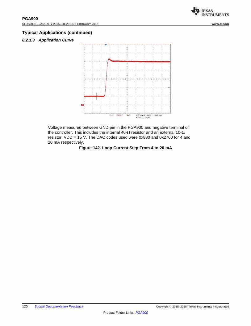
120
PGA900SLDS209B –JANUARY 2015–REVISED FEBRUARY 2018 www.ti.com
Product Folder Links: PGA900
Submit Documentation Feedback Copyright © 2015–2018, Texas Instruments Incorporated
Typical Applications (continued)8.2.1.3 Application Curve
Voltage measured between GND pin in the PGA900 and negative terminal ofthe controller. This includes the internal 40-Ω resistor and an external 10-Ωresistor, VDD = 15 V. The DAC codes used were 0x880 and 0x2760 for 4 and20 mA respectively.
Figure 142. Loop Current Step From 4 to 20 mA

SENSOR
VDD = 3.5V
CONTROLLER
GND
REFCAP
AVDD
RVPVddp
100nF
100nF
GATE
VSUPPLY>30V
100nF
DVDD
DVDD_MEM
AVSS
DVSS
121
PGA900www.ti.com SLDS209B –JANUARY 2015–REVISED FEBRUARY 2018
Product Folder Links: PGA900
Submit Documentation FeedbackCopyright © 2015–2018, Texas Instruments Incorporated
Typical Applications (continued)8.2.2 Using External Depletion MOSFET When Supply to Sensor >30 V With GATE Control
Figure 143. Using External Depletion MOSFET When Supply to Sensor >30 V With GATE ControlDiagram
8.2.2.1 Design RequirementsThere are only a few requirements to take into account when using the PGA900 in a design:• Do not exceed the maximum slew rate of 0.5 V/µs at the VDD pin.• Select an N-channel depletion MOSFET with a gate threshold voltage less than –1.5 V.• A capacitor of 1-nF or less is recommended to be added to the GATE pin.• Place a 100-nF capacitor as close as possible to the AVDD pin.• Place a 100-nF capacitor as close as possible to the DVDD pin.• Place a capacitor between 10 nF and 1000 nF as close as possible to the REFCAP pin.

SENSOR
+VDAC
Vddp
DAC Reference is Absolute 1.25V
40K
S1 -
40
150K
2V/V
4V/V
6.67V/V
S2
40K
10V/V
Open
VOUT
VDD CONTROLLER
GND
REFCAP
DVDD
100nF
100nF
AVDD
100nF
100nF
FBP
FBN
122
PGA900SLDS209B –JANUARY 2015–REVISED FEBRUARY 2018 www.ti.com
Product Folder Links: PGA900
Submit Documentation Feedback Copyright © 2015–2018, Texas Instruments Incorporated
Typical Applications (continued)8.2.2.2 Detailed Design Procedure
8.2.2.2.1 Programmer Tips
Gate control is enabled at power up. If gate drive mode is not used, then the GATE pin must be connected toground and the gate control must be disabled by setting GATE_CTRL_SD bit in ALPWR register to 1.
8.2.3 0- to 10-V Absolute Output With Internal Drive
Figure 144. 0- to 10-V Absolute Output With Internal Drive Diagram
8.2.3.1 Design RequirementsThere are only a few requirements to take into account when using the PGA900 in a design:• Do not exceed the maximum slew rate of 0.5 V/µs at the VDD pin.• Place a 100-nF capacitor as close as possible to the AVDD pin.• Place a 100-nF capacitor as close as possible to the DVDD pin.• Place a capacitor between 10 nF and 1000 nF as close as possible to the REFCAP pin.• Implement compensation, using the COMP pin and an isolation resistor, when driving large capacitive loads
with the VOUT pin.

123
PGA900www.ti.com SLDS209B –JANUARY 2015–REVISED FEBRUARY 2018
Product Folder Links: PGA900
Submit Documentation FeedbackCopyright © 2015–2018, Texas Instruments Incorporated
Typical Applications (continued)8.2.3.2 Detailed Design Procedure
8.2.3.2.1 Programmer Tips
8.2.3.2.1.1 Resetting the Microprocessor and Enable Digital Interface
The following bits have to be configured to reset the M0 microprocessor and to enable digital interface:1. Set IF_SEL bit in MICRO_INTERFACE_CONTROL register to 1.2. Set MICRO_RESET bit in MICRO_INTERFACE_CONTROL register to 1.
8.2.3.2.1.2 Turning on Accurate Reference Buffer (REFCAP Voltage)
The following bits have to be configured to turn ON the accurate reference buffer:1. Set SD bit in ALPWR register to 0.2. Set ADC_EN_VREF bit in ALPWR register to 1.
By turning on the accurate reference buffer, the reference voltage can be measured on REFCAP pin. Further, thecapacitor on REFCAP pin is connected to the reference buffer.
8.2.3.2.1.3 Turning on DAC and DAC GAIN
The following bits have to be configured to turn ON DAC and DAC GAIN:1. Set SD bit in ALPWR register to 0.2. Set ADC_EN_VREF bit in ALPWR register to 1.3. Set DAC_ENABLE in DAC_CTRL_STATUS to 1.4. Set 4_20_MA_EN bit in OP_STAGE_CTRL for voltage output or current output mode.5. Set DACCAP_EN bit in OP_STAGE_CTRL to connect or disconnect external capacitor at DAC output.6. Set DAC_RATIOMETRIC bit in DAC_CONFIG register for ratiometric or absolute voltage output mode.7. Set TEST_MUX_DAC_EN in AMUX_CTRL to 1.

SENSOR
+VDAC
VOUT
Vddp
VDD
GND
REFCAP
DVDD
100nF
100nF
DACCAP
AVDD
100nF
40K
S1 -
FBP
FBN
COMP
40
150K
2V/V
4V/V
6.67V/V
S2
40K
10V/V
Open
DAC Reference is ratiometric to Vddp/4
100nF
CONTROLLER
124
PGA900SLDS209B –JANUARY 2015–REVISED FEBRUARY 2018 www.ti.com
Product Folder Links: PGA900
Submit Documentation Feedback Copyright © 2015–2018, Texas Instruments Incorporated
Typical Applications (continued)8.2.4 0- to 5-V Ratiometric Output With Internal Drive
Figure 145. 0- to 5-V Ratiometric Output With Internal Drive Diagram
8.2.4.1 Design RequirementsThere are only a few requirements to take into account when using the PGA900 in a design:• Do not exceed the maximum slew rate of 0.5 V/µs at the VDD pin.• Place a 100-nF capacitor as close as possible to the AVDD pin.• Place a 100-nF capacitor as close as possible to the DVDD pin.• Place a capacitor between 10 nF and 1000 nF as close as possible to the REFCAP pin.• Implement compensation, using the COMP pin and an isolation resistor, when driving large capacitive loads
with the VOUT pin.

125
PGA900www.ti.com SLDS209B –JANUARY 2015–REVISED FEBRUARY 2018
Product Folder Links: PGA900
Submit Documentation FeedbackCopyright © 2015–2018, Texas Instruments Incorporated
Typical Applications (continued)8.2.4.2 Detailed Design Procedure
8.2.4.2.1 Programmer Tips
8.2.4.2.1.1 Resetting the Microprocessor and Enable Digital Interface
The following bits have to be configured to reset the M0 microprocessor and to enable digital interface:1. Set IF_SEL bit in MICRO_INTERFACE_CONTROL register to 1.2. Set MICRO_RESET bit in MICRO_INTERFACE_CONTROL register to 1.
8.2.4.2.1.2 Turning on Accurate Reference Buffer (REFCAP Voltage)
The following bits have to be configured to turn ON the accurate reference buffer:1. Set SD bit in ALPWR register to 0.2. Set ADC_EN_VREF bit in ALPWR register to 1.
By turning on the accurate reference buffer, the reference voltage can be measured on REFCAP pin. Further, thecapacitor on REFCAP pin is connected to the reference buffer.
8.2.4.2.1.3 Turning on DAC and DAC GAIN
The following bits have to be configured to turn ON DAC and DAC GAIN:1. Set SD bit in ALPWR register to 0.2. Set ADC_EN_VREF bit in ALPWR register to 1.3. Set DAC_ENABLE in DAC_CTRL_STATUS to 1.4. Set 4_20_MA_EN bit in OP_STAGE_CTRL for voltage output or current output mode.5. Set DACCAP_EN bit in OP_STAGE_CTRL to connect or disconnect external capacitor at DAC output.6. Set DAC_RATIOMETRIC bit in DAC_CONFIG register for ratiometric or absolute voltage output mode.7. Set TEST_MUX_DAC_EN in AMUX_CTRL to 1.

SENSOR
+VDAC
Vddp
DAC Reference is Absolute 1.25V
40K
S1 -
40
150K
2V/V
4V/V
6.67V/V
S2
40K
10V/V
Open
VOUT
VDD
GND
REFCAP
DVDD
100nF
100nF
AVDD
100nF
100nF
FBP
FBN
CONTROLLER
126
PGA900SLDS209B –JANUARY 2015–REVISED FEBRUARY 2018 www.ti.com
Product Folder Links: PGA900
Submit Documentation Feedback Copyright © 2015–2018, Texas Instruments Incorporated
Typical Applications (continued)8.2.5 0- to 10-V PWM Output With Internal Drive
Figure 146. 0- to 10-V PWM Output With Internal Drive Diagram
8.2.5.1 Design RequirementsThere are only a few requirements to take into account when using the PGA900 in a design:• Do not exceed the maximum slew rate of 0.5 V/µs at the VDD pin.• Place a 100-nF capacitor as close as possible to the AVDD pin.• Place a 100-nF capacitor as close as possible to the DVDD pin.• Place a capacitor between 10 nF and 1000 nF as close as possible to the REFCAP pin.• Implement compensation, using the COMP pin and an isolation resistor, when driving large capacitive loads
with the VOUT pin.

127
PGA900www.ti.com SLDS209B –JANUARY 2015–REVISED FEBRUARY 2018
Product Folder Links: PGA900
Submit Documentation FeedbackCopyright © 2015–2018, Texas Instruments Incorporated
Typical Applications (continued)8.2.5.2 Detailed Design Procedure
8.2.5.2.1 Programmer Tips
8.2.5.2.1.1 Resetting the Microprocessor and Enable Digital Interface
The following bits have to be configured to reset the M0 microprocessor and to enable digital interface:1. Set IF_SEL bit in MICRO_INTERFACE_CONTROL register to 1.2. Set MICRO_RESET bit in MICRO_INTERFACE_CONTROL register to 1.
8.2.5.2.1.2 Turning on Accurate Reference Buffer (REFCAP Voltage)
The following bits have to be configured to turn ON the accurate reference buffer:1. Set SD bit in ALPWR register to 0.2. Set ADC_EN_VREF bit in ALPWR register to 1.
By turning on the accurate reference buffer, the reference voltage can be measured on REFCAP pin. Further, thecapacitor on REFCAP pin is connected to the reference buffer.
8.2.5.2.1.3 Turning on DAC and DAC GAIN
The following bits have to be configured to turn ON DAC and DAC GAIN:1. Set SD bit in ALPWR register to 0.2. Set ADC_EN_VREF bit in ALPWR register to 1.3. Set DAC_ENABLE in DAC_CTRL_STATUS to 1.4. Set 4_20_MA_EN bit in OP_STAGE_CTRL for voltage output or current output mode.5. Set DACCAP_EN bit in OP_STAGE_CTRL to connect or disconnect external capacitor at DAC output.6. Set DAC_RATIOMETRIC bit in DAC_CONFIG register for ratiometric or absolute voltage output mode.7. Set TEST_MUX_DAC_EN in AMUX_CTRL to 1.
128
PGA900SLDS209B –JANUARY 2015–REVISED FEBRUARY 2018 www.ti.com
Product Folder Links: PGA900
Submit Documentation Feedback Copyright © 2015–2018, Texas Instruments Incorporated
9 Power Supply RecommendationsThe PGA900 has a single pin, VDD, for the input power supply. The maximum slew rate for the VDD pin is 0.5V/µs as specified in the Recommended Operating Conditions. Faster slew rates might generate a POR. Adecoupling capacitor for VDD must be placed as close as possible to the pin.
10 Layout
10.1 Layout GuidelinesStandard layout good practices must be used when designing a board to test the PGA900. Depending on thenumber of layers in the board, one or more GND planes must be inserted as internal layers. In addition, the VDDdecoupling capacitor must be placed as close as possible to the pin. In a similar way, the 100-nF recommendedcapacitors for the AVDD and DVDD regulators as well as the 10- to 1000-nF recommended capacitor forREFCAP must be placed as close as possible to the respective pins.
Depending on the application, the signal traces for FBN, FBP, COMP, and VOUT must be routed such that theydo not cross one another to minimize coupling.
10.2 Layout ExampleThe following figures show the main guidelines previously discussed being implemented in a 6 layers, socketedEVM for the QFN package version of the PGA900. Two main GND planes (layer 2 and 5) were used to provide anearby GND plane to each of the signal layers and the power plane (layer 3) in the EVM. This EVM supportsvoltage and current mode for the device, and as a result, GND separation is needed depending on theapplication. As a result, layer 2 is a solid GND plane for the majority of the circuitry in the EVM (IRETURN).Because most of the circuitry is referred to this GND plane, layers 3 and 4 also contain copper pours connectedto IRETURN. This GND plane is the return path for the supply used in the 4- to 20-mA loop. Layer 5 is a splitplane for the ground references for the digital communication signals used for this EVM (USBGND) and theground pins in the device (GND, AVSS and DVSS), referred to as ASICGND. Figure 147 shows layer 5. TheEVM provides jumpers to connect, or disconnect, these 3 planes one from another depending on the desiredconfiguration.
Figure 148 shows the recommended capacitors for the proper operation of the PGA900. These capacitors areplaced as close as possible to the respective pins from the socket used for this particular EVM. The signal tracesfor FBN, FBP, COMP and VOUT can also be observed to be routed all in the same layer to avoid crossing eachother and minimize coupling.
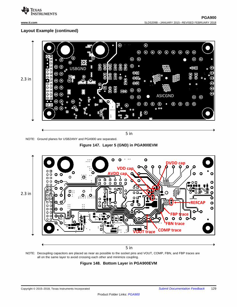
FBP trace
FBN trace
COMP traceVOUT trace
DVDD cap
VDD cap
AVDD cap
REFCAP
2.3 in
5 in
ASICGND
USBGND
2.3 in
5 in
129
PGA900www.ti.com SLDS209B –JANUARY 2015–REVISED FEBRUARY 2018
Product Folder Links: PGA900
Submit Documentation FeedbackCopyright © 2015–2018, Texas Instruments Incorporated
Layout Example (continued)
NOTE: Ground planes for USB2ANY and PGA900 are separated.
Figure 147. Layer 5 (GND) in PGA900EVM
NOTE: Decoupling capacitors are placed as near as possible to the socket pins and VOUT, COMP, FBN, and FBP traces areall on the same layer to avoid crossing each other and minimize coupling.
Figure 148. Bottom Layer in PGA900EVM
130
PGA900SLDS209B –JANUARY 2015–REVISED FEBRUARY 2018 www.ti.com
Product Folder Links: PGA900
Submit Documentation Feedback Copyright © 2015–2018, Texas Instruments Incorporated
11 Device and Documentation Support
11.1 Documentation Support
11.1.1 Related DocumentationFor related documentation see the following:• PGA900 DAC Output Stability Application Note (SLDA020)• PGA900 as 4- to 20-mA Current Loop Transmitter (SLDA030)• Understanding Open Loop Gain of the PGA900 DAC Gain Amplifier (SLDA031)• Connecting PGA900 Instrumentation Amplifier to Resistive Bridge Sensor (SLDA032)• Understanding Open Loop Output Impedance of the PGA900 DAC Gain Amplifier (SLDA033)• System Noise Analysis of a Resistive Bridge Pressure Sensor Connected to the PGA (SLDA034)• PGAxxxEVM-034 User’s Guide (SLDU011)• PGA900 Software User's Guide (SLDU013)• PGA900 GUI User's Guide (SLDU016)
11.2 Receiving Notification of Documentation UpdatesTo receive notification of documentation updates, navigate to the device product folder on ti.com. In the upperright corner, click on Alert me to register and receive a weekly digest of any product information that haschanged. For change details, review the revision history included in any revised document.
11.3 Community ResourcesThe following links connect to TI community resources. Linked contents are provided "AS IS" by the respectivecontributors. They do not constitute TI specifications and do not necessarily reflect TI's views; see TI's Terms ofUse.
TI E2E™ Online Community TI's Engineer-to-Engineer (E2E) Community. Created to foster collaborationamong engineers. At e2e.ti.com, you can ask questions, share knowledge, explore ideas and helpsolve problems with fellow engineers.
Design Support TI's Design Support Quickly find helpful E2E forums along with design support tools andcontact information for technical support.
11.4 TrademarksE2E is a trademark of Texas Instruments.ARM, Cortex are registered trademarks of ARM Ltd.All other trademarks are the property of their respective owners.
11.5 Electrostatic Discharge CautionThese devices have limited built-in ESD protection. The leads should be shorted together or the device placed in conductive foamduring storage or handling to prevent electrostatic damage to the MOS gates.
11.6 GlossarySLYZ022 — TI Glossary.
This glossary lists and explains terms, acronyms, and definitions.
12 Mechanical, Packaging, and Orderable InformationThe following pages include mechanical, packaging, and orderable information. This information is the mostcurrent data available for the designated devices. This data is subject to change without notice and revision ofthis document. For browser-based versions of this data sheet, refer to the left-hand navigation.

PACKAGE OPTION ADDENDUM
www.ti.com 13-Mar-2018
Addendum-Page 1
PACKAGING INFORMATION
Orderable Device Status(1)
Package Type PackageDrawing
Pins PackageQty
Eco Plan(2)
Lead/Ball Finish(6)
MSL Peak Temp(3)
Op Temp (°C) Device Marking(4/5)
Samples
PGA900ARHHR ACTIVE VQFN RHH 36 2500 Green (RoHS& no Sb/Br)
CU NIPDAU Level-2-260C-1 YEAR -40 to 150 PGA900ARHH
PGA900ARHHT ACTIVE VQFN RHH 36 250 Green (RoHS& no Sb/Br)
CU NIPDAU Level-2-260C-1 YEAR -40 to 150 PGA900ARHH
PGA900AYZSR ACTIVE DSBGA YZS 36 1500 Green (RoHS& no Sb/Br)
SNAGCU Level-1-260C-UNLIM -40 to 150 PGA900AYZS
PGA900AYZST ACTIVE DSBGA YZS 36 250 Green (RoHS& no Sb/Br)
SNAGCU Level-1-260C-UNLIM -40 to 150 PGA900AYZS
(1) The marketing status values are defined as follows:ACTIVE: Product device recommended for new designs.LIFEBUY: TI has announced that the device will be discontinued, and a lifetime-buy period is in effect.NRND: Not recommended for new designs. Device is in production to support existing customers, but TI does not recommend using this part in a new design.PREVIEW: Device has been announced but is not in production. Samples may or may not be available.OBSOLETE: TI has discontinued the production of the device.
(2) RoHS: TI defines "RoHS" to mean semiconductor products that are compliant with the current EU RoHS requirements for all 10 RoHS substances, including the requirement that RoHS substancedo not exceed 0.1% by weight in homogeneous materials. Where designed to be soldered at high temperatures, "RoHS" products are suitable for use in specified lead-free processes. TI mayreference these types of products as "Pb-Free".RoHS Exempt: TI defines "RoHS Exempt" to mean products that contain lead but are compliant with EU RoHS pursuant to a specific EU RoHS exemption.Green: TI defines "Green" to mean the content of Chlorine (Cl) and Bromine (Br) based flame retardants meet JS709B low halogen requirements of <=1000ppm threshold. Antimony trioxide basedflame retardants must also meet the <=1000ppm threshold requirement.
(3) MSL, Peak Temp. - The Moisture Sensitivity Level rating according to the JEDEC industry standard classifications, and peak solder temperature.
(4) There may be additional marking, which relates to the logo, the lot trace code information, or the environmental category on the device.
(5) Multiple Device Markings will be inside parentheses. Only one Device Marking contained in parentheses and separated by a "~" will appear on a device. If a line is indented then it is a continuationof the previous line and the two combined represent the entire Device Marking for that device.
(6) Lead/Ball Finish - Orderable Devices may have multiple material finish options. Finish options are separated by a vertical ruled line. Lead/Ball Finish values may wrap to two lines if the finishvalue exceeds the maximum column width.
Important Information and Disclaimer:The information provided on this page represents TI's knowledge and belief as of the date that it is provided. TI bases its knowledge and belief on informationprovided by third parties, and makes no representation or warranty as to the accuracy of such information. Efforts are underway to better integrate information from third parties. TI has taken and

PACKAGE OPTION ADDENDUM
www.ti.com 13-Mar-2018
Addendum-Page 2
continues to take reasonable steps to provide representative and accurate information but may not have conducted destructive testing or chemical analysis on incoming materials and chemicals.TI and TI suppliers consider certain information to be proprietary, and thus CAS numbers and other limited information may not be available for release.
In no event shall TI's liability arising out of such information exceed the total purchase price of the TI part(s) at issue in this document sold by TI to Customer on an annual basis.

TAPE AND REEL INFORMATION
*All dimensions are nominal
Device PackageType
PackageDrawing
Pins SPQ ReelDiameter
(mm)
ReelWidth
W1 (mm)
A0(mm)
B0(mm)
K0(mm)
P1(mm)
W(mm)
Pin1Quadrant
PGA900ARHHR VQFN RHH 36 2500 330.0 16.4 6.3 6.3 1.1 12.0 16.0 Q2
PGA900ARHHT VQFN RHH 36 250 180.0 16.4 6.3 6.3 1.1 12.0 16.0 Q2
PGA900AYZST DSBGA YZS 36 250 180.0 12.4 3.79 3.79 0.71 8.0 12.0 Q1
PACKAGE MATERIALS INFORMATION
www.ti.com 9-Mar-2018
Pack Materials-Page 1
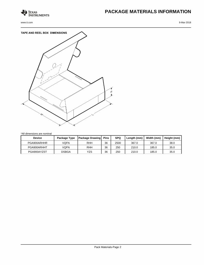
*All dimensions are nominal
Device Package Type Package Drawing Pins SPQ Length (mm) Width (mm) Height (mm)
PGA900ARHHR VQFN RHH 36 2500 367.0 367.0 38.0
PGA900ARHHT VQFN RHH 36 250 210.0 185.0 35.0
PGA900AYZST DSBGA YZS 36 250 210.0 185.0 35.0
PACKAGE MATERIALS INFORMATION
www.ti.com 9-Mar-2018
Pack Materials-Page 2


www.ti.com
PACKAGE OUTLINE
C0.625 MAX
0.2250.175
2.5TYP
2.5TYP
0.5 TYP
0.5 TYP
36X 0.30.2
B E A
D
4219444/A 02/2018
DSBGA - 0.625 mm max heightYZS0036DIE SIZE BALL GRID ARRAY
NOTES: 1. All linear dimensions are in millimeters. Any dimensions in parenthesis are for reference only. Dimensioning and tolerancing per ASME Y14.5M.2. This drawing is subject to change without notice.
BALL A1CORNER
SEATING PLANEBALL TYP 0.05 C
A
1 2 3
0.015 C A B
4 5 6
SYMM
SYMM
B
C
D
E
F
SCALE 5.000
D: Max =
E: Max =
3.745 mm, Min =
3.62 mm, Min =
3.685 mm
3.56 mm
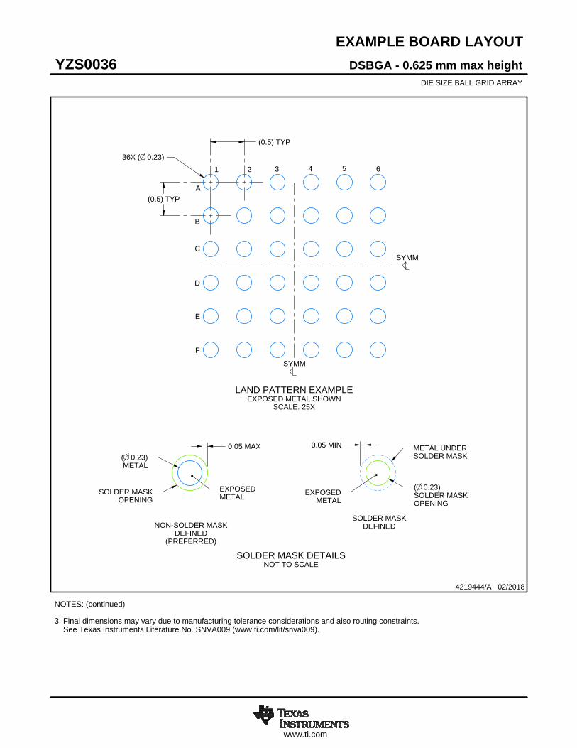
www.ti.com
EXAMPLE BOARD LAYOUT
0.05 MIN0.05 MAX
36X ( 0.23)
(0.5) TYP
(0.5) TYP
( 0.23)SOLDER MASKOPENING
( 0.23)METAL
4219444/A 02/2018
DSBGA - 0.625 mm max heightYZS0036DIE SIZE BALL GRID ARRAY
NOTES: (continued) 3. Final dimensions may vary due to manufacturing tolerance considerations and also routing constraints. See Texas Instruments Literature No. SNVA009 (www.ti.com/lit/snva009).
SOLDER MASK DETAILSNOT TO SCALE
SYMM
SYMM
C
1 2 3 4 5 6
A
B
D
E
F
LAND PATTERN EXAMPLEEXPOSED METAL SHOWN
SCALE: 25X
NON-SOLDER MASKDEFINED
(PREFERRED)
EXPOSEDMETAL
SOLDER MASKOPENING
SOLDER MASKDEFINED
METAL UNDERSOLDER MASK
EXPOSEDMETAL

www.ti.com
EXAMPLE STENCIL DESIGN
(0.5) TYP
(0.5) TYP
36X ( 0.25) (R0.05) TYP
4219444/A 02/2018
DSBGA - 0.625 mm max heightYZS0036DIE SIZE BALL GRID ARRAY
NOTES: (continued) 4. Laser cutting apertures with trapezoidal walls and rounded corners may offer better paste release.
SYMM
SYMM
1 2 3 4 5 6
C
A
B
D
E
F
SOLDER PASTE EXAMPLEBASED ON 0.1 mm THICK STENCIL
SCALE: 25X
METALTYP

IMPORTANT NOTICE
Texas Instruments Incorporated (TI) reserves the right to make corrections, enhancements, improvements and other changes to itssemiconductor products and services per JESD46, latest issue, and to discontinue any product or service per JESD48, latest issue. Buyersshould obtain the latest relevant information before placing orders and should verify that such information is current and complete.TI’s published terms of sale for semiconductor products (http://www.ti.com/sc/docs/stdterms.htm) apply to the sale of packaged integratedcircuit products that TI has qualified and released to market. Additional terms may apply to the use or sale of other types of TI products andservices.Reproduction of significant portions of TI information in TI data sheets is permissible only if reproduction is without alteration and isaccompanied by all associated warranties, conditions, limitations, and notices. TI is not responsible or liable for such reproduceddocumentation. Information of third parties may be subject to additional restrictions. Resale of TI products or services with statementsdifferent from or beyond the parameters stated by TI for that product or service voids all express and any implied warranties for theassociated TI product or service and is an unfair and deceptive business practice. TI is not responsible or liable for any such statements.Buyers and others who are developing systems that incorporate TI products (collectively, “Designers”) understand and agree that Designersremain responsible for using their independent analysis, evaluation and judgment in designing their applications and that Designers havefull and exclusive responsibility to assure the safety of Designers' applications and compliance of their applications (and of all TI productsused in or for Designers’ applications) with all applicable regulations, laws and other applicable requirements. Designer represents that, withrespect to their applications, Designer has all the necessary expertise to create and implement safeguards that (1) anticipate dangerousconsequences of failures, (2) monitor failures and their consequences, and (3) lessen the likelihood of failures that might cause harm andtake appropriate actions. Designer agrees that prior to using or distributing any applications that include TI products, Designer willthoroughly test such applications and the functionality of such TI products as used in such applications.TI’s provision of technical, application or other design advice, quality characterization, reliability data or other services or information,including, but not limited to, reference designs and materials relating to evaluation modules, (collectively, “TI Resources”) are intended toassist designers who are developing applications that incorporate TI products; by downloading, accessing or using TI Resources in anyway, Designer (individually or, if Designer is acting on behalf of a company, Designer’s company) agrees to use any particular TI Resourcesolely for this purpose and subject to the terms of this Notice.TI’s provision of TI Resources does not expand or otherwise alter TI’s applicable published warranties or warranty disclaimers for TIproducts, and no additional obligations or liabilities arise from TI providing such TI Resources. TI reserves the right to make corrections,enhancements, improvements and other changes to its TI Resources. TI has not conducted any testing other than that specificallydescribed in the published documentation for a particular TI Resource.Designer is authorized to use, copy and modify any individual TI Resource only in connection with the development of applications thatinclude the TI product(s) identified in such TI Resource. NO OTHER LICENSE, EXPRESS OR IMPLIED, BY ESTOPPEL OR OTHERWISETO ANY OTHER TI INTELLECTUAL PROPERTY RIGHT, AND NO LICENSE TO ANY TECHNOLOGY OR INTELLECTUAL PROPERTYRIGHT OF TI OR ANY THIRD PARTY IS GRANTED HEREIN, including but not limited to any patent right, copyright, mask work right, orother intellectual property right relating to any combination, machine, or process in which TI products or services are used. Informationregarding or referencing third-party products or services does not constitute a license to use such products or services, or a warranty orendorsement thereof. Use of TI Resources may require a license from a third party under the patents or other intellectual property of thethird party, or a license from TI under the patents or other intellectual property of TI.TI RESOURCES ARE PROVIDED “AS IS” AND WITH ALL FAULTS. TI DISCLAIMS ALL OTHER WARRANTIES ORREPRESENTATIONS, EXPRESS OR IMPLIED, REGARDING RESOURCES OR USE THEREOF, INCLUDING BUT NOT LIMITED TOACCURACY OR COMPLETENESS, TITLE, ANY EPIDEMIC FAILURE WARRANTY AND ANY IMPLIED WARRANTIES OFMERCHANTABILITY, FITNESS FOR A PARTICULAR PURPOSE, AND NON-INFRINGEMENT OF ANY THIRD PARTY INTELLECTUALPROPERTY RIGHTS. TI SHALL NOT BE LIABLE FOR AND SHALL NOT DEFEND OR INDEMNIFY DESIGNER AGAINST ANY CLAIM,INCLUDING BUT NOT LIMITED TO ANY INFRINGEMENT CLAIM THAT RELATES TO OR IS BASED ON ANY COMBINATION OFPRODUCTS EVEN IF DESCRIBED IN TI RESOURCES OR OTHERWISE. IN NO EVENT SHALL TI BE LIABLE FOR ANY ACTUAL,DIRECT, SPECIAL, COLLATERAL, INDIRECT, PUNITIVE, INCIDENTAL, CONSEQUENTIAL OR EXEMPLARY DAMAGES INCONNECTION WITH OR ARISING OUT OF TI RESOURCES OR USE THEREOF, AND REGARDLESS OF WHETHER TI HAS BEENADVISED OF THE POSSIBILITY OF SUCH DAMAGES.Unless TI has explicitly designated an individual product as meeting the requirements of a particular industry standard (e.g., ISO/TS 16949and ISO 26262), TI is not responsible for any failure to meet such industry standard requirements.Where TI specifically promotes products as facilitating functional safety or as compliant with industry functional safety standards, suchproducts are intended to help enable customers to design and create their own applications that meet applicable functional safety standardsand requirements. Using products in an application does not by itself establish any safety features in the application. Designers mustensure compliance with safety-related requirements and standards applicable to their applications. Designer may not use any TI products inlife-critical medical equipment unless authorized officers of the parties have executed a special contract specifically governing such use.Life-critical medical equipment is medical equipment where failure of such equipment would cause serious bodily injury or death (e.g., lifesupport, pacemakers, defibrillators, heart pumps, neurostimulators, and implantables). Such equipment includes, without limitation, allmedical devices identified by the U.S. Food and Drug Administration as Class III devices and equivalent classifications outside the U.S.TI may expressly designate certain products as completing a particular qualification (e.g., Q100, Military Grade, or Enhanced Product).Designers agree that it has the necessary expertise to select the product with the appropriate qualification designation for their applicationsand that proper product selection is at Designers’ own risk. Designers are solely responsible for compliance with all legal and regulatoryrequirements in connection with such selection.Designer will fully indemnify TI and its representatives against any damages, costs, losses, and/or liabilities arising out of Designer’s non-compliance with the terms and provisions of this Notice.
Mailing Address: Texas Instruments, Post Office Box 655303, Dallas, Texas 75265Copyright © 2018, Texas Instruments Incorporated