Peter Göttlicher | CALICE | Heidelberg, September 15 th 2011 | Page 1 Peter Göttlicher, DESY-FEB...
18
Peter Göttlicher | CALICE | Heidelberg, September 15 th 2011 | Page 1 Peter Göttlicher, DESY-FEB Heidelberg September 15 th , 2011 A concept for power cycling the electronics of CALICE
-
Upload
quentin-bertram-wright -
Category
Documents
-
view
217 -
download
1
Transcript of Peter Göttlicher | CALICE | Heidelberg, September 15 th 2011 | Page 1 Peter Göttlicher, DESY-FEB...

Peter Göttlicher | CALICE | Heidelberg, September 15th 2011 | Page 1
Peter Göttlicher, DESY-FEB
HeidelbergSeptember 15th, 2011
A concept for power cyclingthe electronics of CALICE

Peter Göttlicher | CALICE | Heidelberg, September 15th 2011 | Page 2
Outline
>Motivation for power cycling
> Building blocks for power cycling
> Alternatives
>Consequences for power supplies
> Summary

Peter Göttlicher | CALICE | Heidelberg, September 15th 2011 | Page 3
Motivation: Power Cycling to avoid active Cooling
Very slow, butfor long times Þ NeedPower cyclingTo keep heat up below 0.50C
Simplified model:- No heat transfer radial “bad due to sandwich”- Octagon as cylinder: No heat transfer in f- Symmetry at IP-plane
Mechanical design constraint:- No cooling within calorimeter to keep homogeneity and simplicity- Cooling only at service end
Solution:Parabel + Fourier terms
0.0 0.5 1.0 1.5 2.0 z = Position along beam axis [m]
Tem
pera
ture
incr
ease
[K]
0.0
0.1
0.2
0.3
𝜕𝑇𝜕𝑡
= 1h𝑒𝑎𝑡 𝑐𝑎𝑝 . /𝑎𝑟𝑒𝑎
𝑝𝑜𝑤𝑒𝑟𝑎𝑟𝑒𝑎 |
𝑒𝑙𝑒𝑐𝑡𝑟𝑜𝑛𝑖𝑐𝑠
+h𝑒𝑎𝑡 𝑐𝑜𝑛𝑑𝑢𝑐𝑡𝑖𝑣𝑖𝑡𝑦 𝜕2𝑇𝜕𝑧 2
Z=0m
Z=2.2m
Motivation
Details see: P.Göttlicher, TWEPP-07, Prague, proceedings Page 296
40µW/channel

Peter Göttlicher | CALICE | Heidelberg, September 15th 2011 | Page 4
Building Blocks for the Power System
1. Planes with scintillators and SiPM’s, ASIC’s and PCB’s
4. Power supply
2. End of layer electronics
DAQ is Optical:No issue for EMI
3. cable
Building blocks
5. Definitionof GNDElectronics and GNDPE
Peter Göttlicher | CALICE | Heidelberg, September 15th 2011 | Page 5
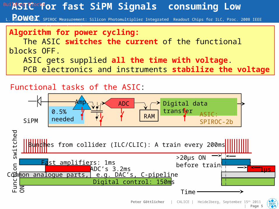
ASIC for fast SiPM Signals consuming Low Power
Bunches from collider (ILC/CLIC): A train every 200ms
Algorithm for power cycling:The ASIC switches the current of the functional blocks OFF.ASIC gets supplied all the time with voltage.PCB electronics and instruments stabilize the voltage
L. Raux et al., SPIROC Measurement: Silicon Photomultiplier Integrated Readout Chips for ILC, Proc. 2008 IEEE Nuclear Science Symposium (NSS08)
Functional tasks of the ASIC:
0.5%needed
ADC Digital data transfer
RAM ASIC: SPIROC-2b
SiPM
Amp.
Fast amplifiers: 1msADC’s 3.2ms
Common analogue parts, e.g. DAC’s, C-pipelineDigital control: 150ms
>20µs ON before train
1µs
Building blocks
Time Fun
ctio
n sw
itche
d O
N

Peter Göttlicher | CALICE | Heidelberg, September 15th 2011 | Page 6
ASIC as current switch
Measurements:- Inductive current probes Slow: 0.25 – 50MHz
Fast: 30MHz-3GHz
- Setup: ASIC+ capacitors on a PCB
- Expectation is ~40mA/ASIC, summed over all pins Measurement influence I-distribution to pins
GND pin (1 of 2) of ASIC
Expected waveform, Amplitude is arb. units.
High pass of probe
Measured currents at the GND-supply of ASIC
Slow probe
Fast probe
GND pin (1 of 2) of ASIC
Voltage pin (1 of 3) for preamplifier
Tantal capacitor
0 200 400 600 [ns] time
-20 0 20 40 60 [ns] time
10mA/pin
System has to deal with: EMI: electromagnetic interference - Wide frequencies 5Hz to few 100MHz- Huge currents 2.2A for a layer,
3.4kA for AHCAL-barrel
30mA/pin
Building blocks
Bandpass:
Peter Göttlicher | CALICE | Heidelberg, September 15th 2011 | Page 7
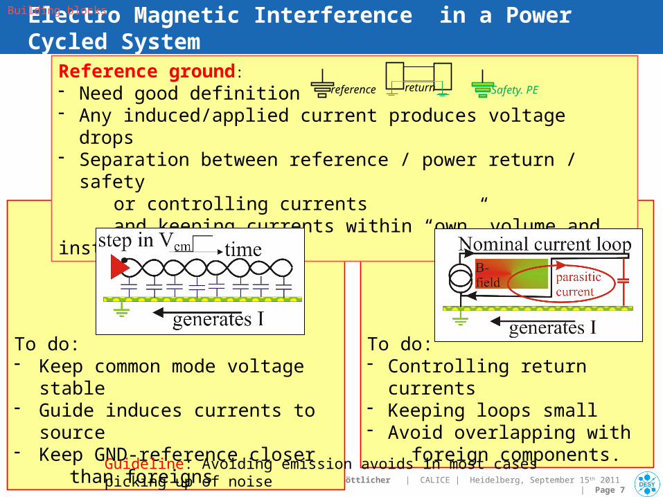
Current loops
To do:- Controlling return currents- Keeping loops small- Avoid overlapping with foreign components.
Capacitive coupling
To do:- Keep common mode voltage stable- Guide induces currents to source- Keep GND-reference closer than foreigns
Electro Magnetic Interference in a Power Cycled System
Reference ground:- Need good definition- Any induced/applied current produces voltage drops- Separation between reference / power return / safety or controlling currents and keeping currents within “own” volume and instrumentation
Guideline: Avoiding emission avoids in most cases picking up of noise
reference return Safety. PE
Building blocks

Peter Göttlicher | CALICE | Heidelberg, September 15th 2011 | Page 8
Keeping the high Frequencies local: PCB itself
36 x 36 cm PCBwith scintillators, SiPM’s LED
144mA switched current
Part of a thin cassette between absorber layer of HCAL
Layer structure of PCB:
By that one get- a thin PCB and also- A good high frequency capacitor 60pF/cm2
- Layout with short distance to via maintain the performance.
Simulation model:“two diomensional delay line”
1cm x 1cm
Capacitor well known:
One-dimensional delay well known
Inductivity:
Building blocks
GND d PCB= 50-60µmVsupply
GND

Peter Göttlicher | CALICE | Heidelberg, September 15th 2011 | Page 9
Tantal
Voltage for ASIC stabilized by local discrete Capacitors
Total:12 Tantal/4 ASIC’s+ 17 ceramics+ PCB
PCB, alone
Tantal, AVX, 33µF
Murata, 100nf
Murata, 10nf
Murata, 2.2nf
Murata, 1nf
Ceramics X7R
1kHz 1MHz 1GHz
Impe
danc
e Z
=|U
|/|I|
Frequency
900
-900U to
I ph
ase
shift
00
ASIC is supported overwide frequency rangewith Z< 0.1W144mA generates <20mV
Oscillations are dumpedfor wide frequency range with phase ¹ ±900
Trust in simulation:- <1.5GHz=(1/10) granularity- No resistive behavior of ASIC is included. That over estimates the resonances at high frequencies
Result:- Locally good for > 10kHz- Additional effort < 10kHz
0.1 W
1 W
10 W
100 W
00.1 W
Capacitors mounted to the 36x36cm2 PCBSimulation of voltage induced by current
ceramicPCB-layer
Dominated by:
Capacitor like
Coil like
Building blocks

Peter Göttlicher | CALICE | Heidelberg, September 15th 2011 | Page 10
Low frequency charge storage for < 10kHz
At end of layer,there is a bit of - space- cooling
Concept:- Charge for the train stored in a capacitor C2
- Voltage drop allowed ~ 0.6V- Fast voltage regulator - Charge for faster reaction is within the distributed capacitors + C3
C2 = 3.4mF bank of few Tantala voltage regulator with external FET > 2AC3+distributed = 2mF
C2C3
Building blocks

Peter Göttlicher | CALICE | Heidelberg, September 15th 2011 | Page 11
Voltage at ASIC: Measurement
Control electronicsfor layer
Reduced test setup: Control board, 1 interconnect, 1 board
Tantal taken away
Default setup
Tantal moved to control board
Power onCommand,step in IASIC
Su
pp
ly v
olta
ge
of A
SIC
(A
C-c
om
po
ne
nt)
[m
V]
GNDelectronics
2m2/Layer1.3mm distance C=13nF
4mV
Stainless steel absorber= GNDPE
Þ OK, even with extrapolation to 1500 layers low?Investigations of reason and improvements possible, to be watched
Time [ns]
Voltage step: - Measured 4mV, 400ns- Extrapolate to full system
< 80mV at far endOK for operation, over-,undervoltage, time, …
Induces current into GNDPE, if step is on GNDelectronics
< 2 mA per layer
Building blocks

Peter Göttlicher | CALICE | Heidelberg, September 15th 2011 | Page 12
Definition of GND-point: - good for keeping sensitive SiPM’s stable - single connection to reduce currents in GNDPE system
Connection of GNDElectronics and GNDPE
Control electronicsfor layer
GNDelectronics
2m2/Layer1.3mm distance C=13nF Stainless
steel absorber= GNDPE
Building blocks
Parasitic:Single PE: 105-106e-
SiPM
scintillator
The SiPM should not pickup noise from a floating PE-system: Connect as close as possible from GNDElectronics to GNDPE Þ Low Impedance connection and not large wire loopsÞ Option as long as it is near by
more connections within cassette, but risk of currents in the PE-system
Mechanical easy accessible is the point as the end of layer at the DIF Nearest accessible point, at the layer (>100MHz) rely on: CLAYER_to_PE
highest freqencies: - amplifier_auto-trigger- power switchingl/10:
Few cm

Peter Göttlicher | CALICE | Heidelberg, September 15th 2011 | Page 13
Integrating to Infrastructure
70pF/m from cable to support
ASICasswitchedcurrent sink
50m cable, 1mm2, on a cable support
0 1 2 3 4 5 [ms] 6time
nA0
-40
-80
-120
-160
Cur
rent
per
laye
r
Current induced into GNDPE
𝜏=0.1𝑚𝑠
𝜏=1𝑚𝑠
𝜏=10𝑚𝑠
𝜏=100𝑚𝑠
Simulation of cable
𝜏=𝑅𝐶
Impact of cable is a combination of choices:- Input filter: R=10W, C=1mF reasonable mechanical size EMI better t=100ms- Power supply behavior here neglected capacitance to PE, might be 2 order of magnitude larger than cable! Here: ideal V-source- Mechanical integration and
galvanic isolation per (group or) layer and pair of wires for it
With 1500 layers of AHCAL: IPE=120mA Really small, Ideal! No parasitic, C+=C-! Don’t be too reluctant in EMI-rules
Building blocks
C-,C+
Ideal No parasitics no parameter spreadC+=C-

Peter Göttlicher | CALICE | Heidelberg, September 15th 2011 | Page 14
Current in Supply Cable
Control electronicsfor layer
Reduced test setup: Control board, 1 interconnect, 1 board, Short cable to laboratory supply
Cur
rent
per
1/1
8 la
yer
in s
uppl
y ca
ble
[m
A] Preamplifiers ON ADC’s ON
Work bench settings
Without input filter with input filter t=10ms
Input filter important tolower amplitude fluctuationsand remaining frequencies within cableImportant: EMI-crosstalk to others
Frequencies are lowElectronics like to have larger tto smoothen further ÛMechanics easier in service-hall
Building blocks

Peter Göttlicher | CALICE | Heidelberg, September 15th 2011 | Page 15
Cabling a multi layer calorimeter:
Six such cables would allow 48 layers- Individual connected and galvanic isolation outside ILD or as compromise filter with ferrits
- Additional covers, tubes for flammability? Special production: wires/cable optimized
- On picture 4 x 0.5mm2 : 12V (LED) just from DESY-stock 6V ASIC, FPGA, … GND Bias (120V) Locally 0.5mm2 would be fine For 50m 1mm2 or more would be better Issue is less than a factor 2 in cross section!
- It is work to manufacture! But feasible for 1500 layers!
- How many wire per cable? Small total cross section or good bending?
An idea but not the only and not work through! Two layers grouped:Still easy low-L access to GNDPE
DIF
DIF steel
Split point of wire
Components on board
Option ?: Less power supply channels
Group of wires

Peter Göttlicher | CALICE | Heidelberg, September 15th 2011 | Page 16
Alternatives: Star grounding
Large loops
Parasitic current from loop 1:Worsened for:- Common return paths to own and foreign
Cross talks and pickup noise- It will not stay locally for low frequencies
Loop 1
LargeInductance:SiPM surroundingis worsened Transformers to
own and foreign
Antenna
Frequency dependent:PE is whole metal structure of ILD
Also to ILD magnet: Quench or fast discharge not yet studied, but larger loops are worse: Resistance needed?
Power routing has to be parallel to GND rooting with low L and R>L*w But points are not points, they have a size
Nowadays: Systems have noise from switching power and faster digital edges It’s a system issue and therefore tends to appear late completeness of ILD and risk at all modifications
ConnectorsHas to withstandgroup current

Peter Göttlicher | CALICE | Heidelberg, September 15th 2011 | Page 17
Consequences per power supply
Multichannel systems are available with basic features- With galvanic isolation per channel- Low ripple: 5-10(20) mVppTheir development was (partially) driven by researchWIENER, CAEN, ISEG, and ??????
Comparison of AHCAL needs to a WIENER systemAHCAL: (not final, not optimized/fully understood) - Group of three voltages allowed - 6V/1-2A, 12V/0.1A, 120V/5mA at DIF-- Up to now: constant voltage with over current trip is studied Option: Constant current or impedance controlled, if performance gets better - 1500 layers …. 4500 voltages see option to group 2 layers - Low ripple/noise because sensitive ILD-detector - Floating to PE, limited to ±24V? - Small coupling to GNDPE, but good EMI compared: 50m cable on PE: 3.5nF. - Cope with fluctuation current: typical: 800mA/layer, 2ms
MPOD just because other project
- Single chan.,- 50W per channel- Constant V with over current trip
- Just 80chan/crate, but each 50W.- 5-10mVpp
To be done?Longer scale or next steps:
Adaptation/development:- Research center/industry?- Can lower power be converted to more channels? … if 1 to 1in power : More than 400 channels per crate
Getting fast running:- Selecting a system and buy - Programming for combined power supply and DIF/uC

Peter Göttlicher | CALICE | Heidelberg, September 15th 2011 | Page 18
Summary
Power cycling allows to reduce heat by factor 100!
Coherent fast switching ON/OFF of high current: CALICE-AHCAL: 2.2A*layers : 3.4kA for the barrel
5Hz to few 100MHz System aspects at local design…. Not only power-pulsing also EMI - Local defined return-paths for current - Local charge storage for wide frequency range that keeps
- the impedance small- the currents leaving a defined volume small with slow rise times
System aspects within the infrastructure Lower frequency part handled by cables and power supply Good integration of power supplies and cables.
Simulation leaves many parasitic/accuracy effects out Underestimates the high frequency EMI-disturbance
…. Experiments, concepts to be better than simulation promises
Experimental setups and integration into ILD to be continued