Perspectives on Physics: Organic Electronics and Spintronics · Perspectives on Physics: Organic...
54
Perspectives on Physics: Organic Electronics and Spintronics Prof. Mats Fahlman Surface Physics and Chemistry division, ifm [email protected]
Transcript of Perspectives on Physics: Organic Electronics and Spintronics · Perspectives on Physics: Organic...

Perspectives on Physics: Organic Electronics and
SpintronicsProf. Mats Fahlman
Surface Physics and Chemistry division, ifm

24/04/2009 Mats Fahlman, LiU
1 000
Stone, Wood, Copper Copper, Bronze,
Paper, GlassIron
1 800
Rubber,Steel
1 940
Steel alloys,Light alloys,
Cement,Polymers
(Nylon, etc)
20041970
Silicon!,Super Alloys
Conducting Polymers,Liquid Crystals,
Electrochromic mat.Optical fibers,
Fullerenes,Nanotubes,GMR, etc,
1 000
Stone, Wood, Copper Copper, Bronze,
Paper, GlassIron
1 800
Rubber,Steel
1 940
Steel alloys,Light alloys,
Cement,Polymers
(Nylon, etc)
20041970
Silicon!,Super Alloys
Conducting Polymers,Liquid Crystals,
Electrochromic mat.Optical fibers,
Fullerenes,Nanotubes,GMR, etc,
New Materials: a simple time line
2009
24/04/2009 Mats Fahlman, LiU
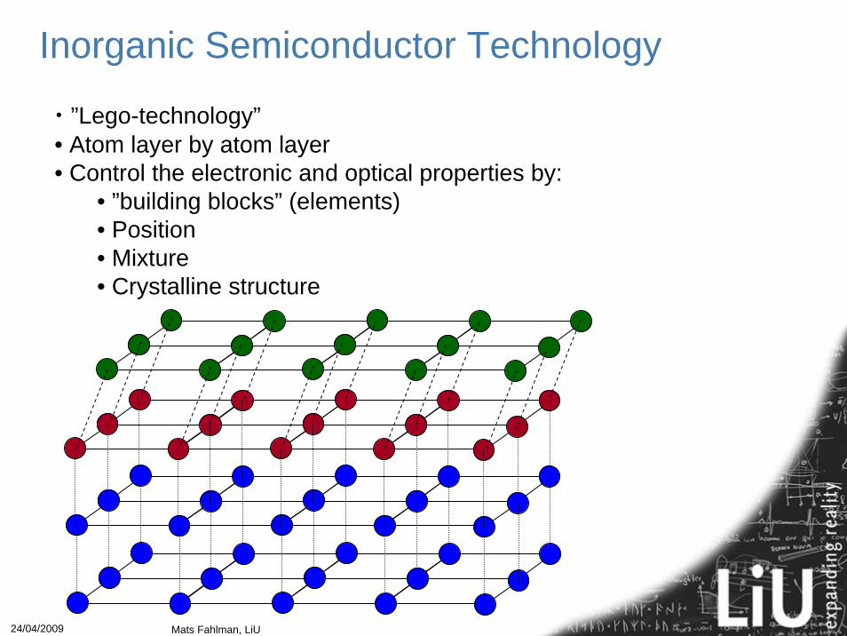
Inorganic Semiconductor Technology
• ”Lego-technology”• Atom layer by atom layer• Control the electronic and optical properties by:
• ”building blocks” (elements)• Position• Mixture• Crystalline structure
24/04/2009 Mats Fahlman, LiU
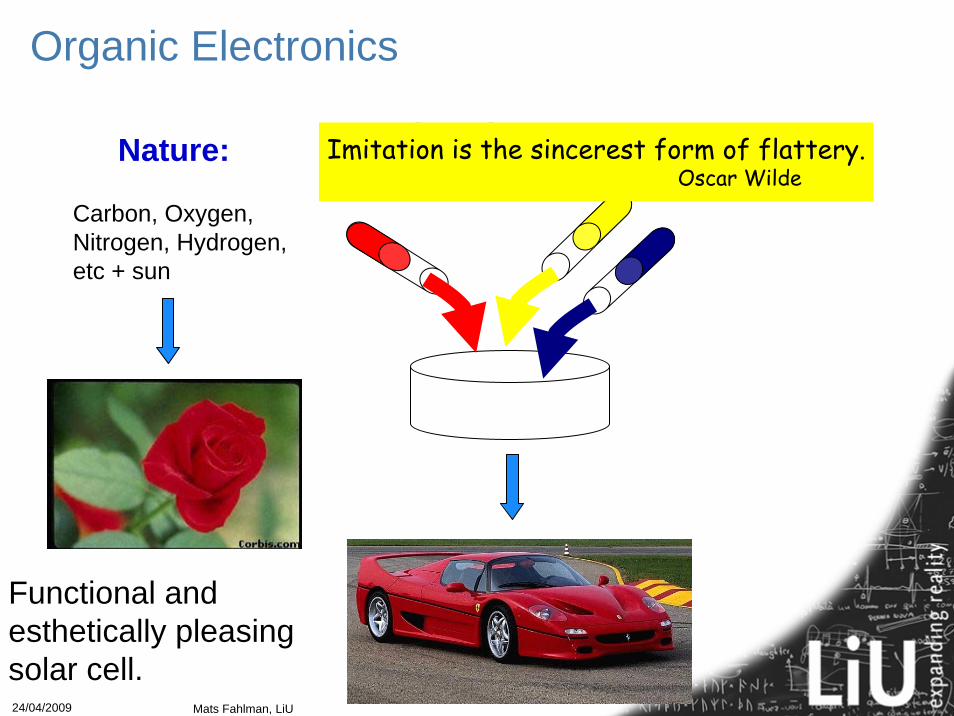
Organic Electronics
Nature:
Carbon, Oxygen, Nitrogen, Hydrogen, etc + sun
Functional and esthetically pleasingsolar cell.
The “dream”:Imitation is the sincerest form of flattery.Oscar Wilde

24/04/2009 Mats Fahlman, LiU
Nobel Prize in Chemistry 2000
”…for the discovery and developmentof conducting polymers.”
• Prof. A.J. Heeger• Prof. A.G. MacDiarmid• Prof. H. Shirakawa
1977
Polyacetylene (PA)
CC
CC
CC
CH
H
H
H
H
H
H
I2σ = 10-9 S/cm σ = 38 S/cm

24/04/2009 Mats Fahlman, LiU
Conjugated polymers
10-18 10-14 10-10 10-6 10-2 102 106S/cm
Qua
rtz
Dia
mon
d
Gla
ss
Silic
on
Ger
man
ium
Cop
per
Insulators Semi-Conductors
Metals
Polymers: Insulators and Metals

24/04/2009 Mats Fahlman, LiU
S
O O
S
O O
S+
O O
S
O O
CH2* CH *
C
NH
On
CCH3
CH3
CH2 SO3H
NNH
NH* N *x y n
**
n
SO3H
CH2* CH *
C
NH2
O
n
a)
b)
c) d) e)
* *n
C8H17 C8H17poly(dioctyl-fluorene)
S
S
S
S
n
R R
R R
Semiconductors
Insulators
PolymersMetals
Doping

24/04/2009 Mats Fahlman, LiU
Polymers can exist as:
Linear chains
Cross-linked chains Networks
Chemically identical polymers can have completely differentproperties depending on degree of cross-linking
Polymer Chains

24/04/2009 Mats Fahlman, LiU
Organic Electronics
Conducting Polymers in solution = Electronic InkThe Goal: Organic electronics printed onto paper/plastic
•Applications:- Sensors in food packaging- Large area displays-RF-ID (Barcodes, Security tags, etc)- Photovoltaics
• Cheap!• Environmentally compatible
- recycling• Existing printing techniques:
- Screen, Off-set, Ink-jet,etc
24/04/2009 Mats Fahlman, LiU
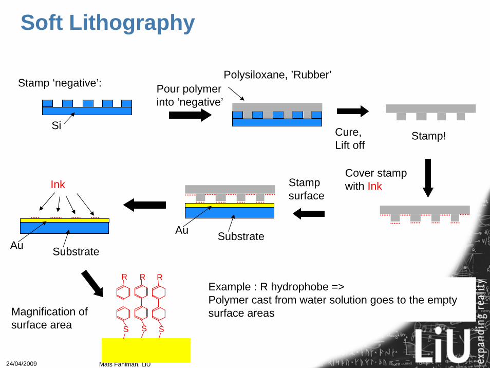
Si
Stamp ‘negative’:Polysiloxane, ’Rubber’
Pour polymerinto ‘negative’
Cure,Lift off
Stamp!
Cover stampwith InkStamp
surface
Au SubstrateAu Substrate
Ink
S S S
R R R
Magnification ofsurface area
Example : R hydrophobe =>Polymer cast from water solution goes to the empty surface areas
Soft Lithography
24/04/2009 Mats Fahlman, LiU
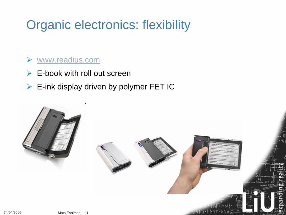
Organic electronics: flexibility
www.readius.com
E-book with roll out screen
E-ink display driven by polymer FET IC

24/04/2009 Mats Fahlman, LiU
E0
Energy of the orbital(Defined as negative)
Compare with satellite orbiting the earth
Atom nucleus
Electron-orbitals
Unlike satellites, electrons can only existin certain orbits with certain energies(quantum mechanics).
Atoms: the electron orbitals

24/04/2009 Mats Fahlman, LiU
Fermions• Electrons are fermions• Have spin 1/2• Can’t have the same quantum state (Pauli principle)• Only two e- per energy level (orbital)
E0
Bosons• Photons are bosons• Have integer spin• Can have identical quantumstates• “Unlimited” number per energylevel (orbital)
E0
ω
ω
e-
Electron spin:
Fermions - Bosons

24/04/2009 Mats Fahlman, LiU
E
E Ek
Many atoms => fine structure of many split levels with small ΔE => ‘bands’

24/04/2009 Mats Fahlman, LiU
the hydrogen atom is the only system found in our world which we can describeexactly with quantum mechanics.... for all others, approximations.
ΨΨΨ )(22 ,
22
22
pepp
ee
rVmmt
i rhhh +⎟
⎟⎠
⎞⎜⎜⎝
⎛∇−∇−=
∂∂
Ψ
h
)( , perV r
per ,r
the wave function describing the motion of the proton and the electron;
h "bar" = Planck's constant (h) divided by 2π;
me , mp the electron mass and the proton mass;
the Coulomb potential;
the position of electron and proton, respectively;
∇e2, ∇p
2 Laplace operators (2nd derivative in space coordinates) for the electron and proton.
Wave mechanics of the hydrogen atom

24/04/2009 Mats Fahlman, LiU
Ψ-= {2(1-S)}-1/2(A - B)
Ψ+= {2(1+S)}-1/2(A + B)
The hydrogen molecular ion (H2)
24/04/2009 Mats Fahlman, LiU
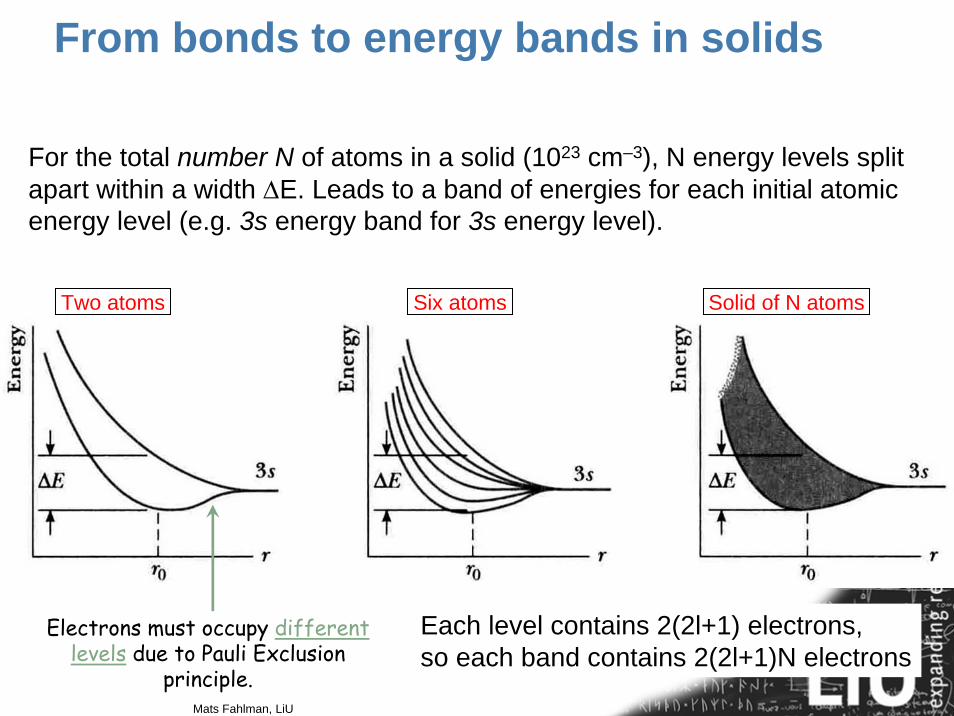
Solid of N atomsTwo atoms Six atoms
For the total number N of atoms in a solid (1023 cm–3), N energy levels split apart within a width ΔE. Leads to a band of energies for each initial atomic energy level (e.g. 3s energy band for 3s energy level).
Electrons must occupy different levels due to Pauli Exclusion
principle.
Each level contains 2(2l+1) electrons, so each band contains 2(2l+1)N electrons
From bonds to energy bands in solids

24/04/2009 Mats Fahlman, LiU
InsulatorLarge Eg
Eg
Diamond
SemiconductorMedium Eg
Eg
Si
MetalEg ~ 0
Fe
Electrons are fermions: limited numberper band!

24/04/2009 Mats Fahlman, LiU
Metal
24/04/2009 Mats Fahlman, LiU
Under constructionUnder construction
Semiconductor & Insulator

24/04/2009 Mats Fahlman, LiU
S.R. Forrest, MRS bulletin, January 2005
Photocurrent generation: Organic Solar Cells

24/04/2009 Mats Fahlman, LiUDonors Acceptors
• Soluble in samesolvents
• Phase segregatesinto networks
• Band offsets facilitate chargetransfer
Polymer solar cells: Donor and acceptormaterials

24/04/2009 Mats Fahlman, LiU
Light
R.A.J. Janssen, MRS bulletin, January 2005
Bulk heterojunction solar cells
24/04/2009 Mats Fahlman, LiU
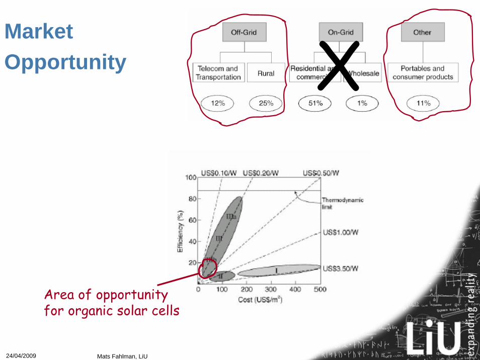
Area of opportunityfor organic solar cells
XMarketOpportunity
24/04/2009 Mats Fahlman, LiU
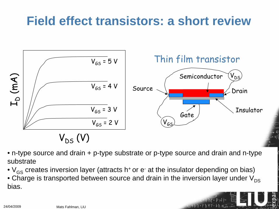
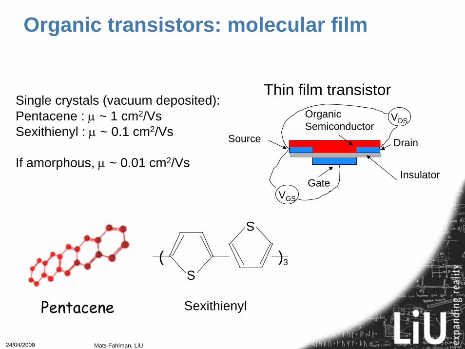
Thin film transistorSemiconductor
DrainSource
GateInsulator
VGS
VDS
VDS (V)
I D(m
A)
VGS = 2 V
VGS = 3 V
VGS = 4 V
VGS = 5 V
• n-type source and drain + p-type substrate or p-type source and drain and n-type substrate• VGS creates inversion layer (attracts h+ or e- at the insulator depending on bias)• Charge is transported between source and drain in the inversion layer under VDSbias.
Field effect transistors: a short review
24/04/2009 Mats Fahlman, LiU
Thin film transistorOrganicSemiconductor
DrainSource
GateInsulator
VGS
VDS
Single crystals (vacuum deposited):Pentacene : μ ~ 1 cm2/VsSexithienyl : μ ~ 0.1 cm2/Vs
If amorphous, μ ~ 0.01 cm2/Vs
Pentacene
S
S
( )3
Sexithienyl
Organic transistors: molecular film

24/04/2009 Mats Fahlman, LiU
Thin film transistorOrganicSemiconductor
DrainSource
GateInsulator
VGS
VDS
Ordered films (solution deposited):Polyhexyltiophene : μ ~ 0.1 cm2/Vs
Disordered films (solution deposited):Polyhexyltiophene : μ ~ 10-4 cm2/VsPoly(p-penylenevinylene) : μ ~ 10-4 cm2/VsPolyfluorene: μ ~ 10-3-10-4 cm2/Vsetc
Polythiophene, PTS n
Polyfluorene, PFOn
RR
Polymer transistors

24/04/2009 Mats Fahlman, LiU
r
invD t
WLQI −= DSinvD VLWQI μ−=
DSTGSoxD V)VV(LWCI −μ=
Linear region:
LVEv DSμ=μ=
vLt r = and
)VV(CQ TGSoxinv −−=
S D
L
WQinv = Charge per unit area in inversion layertr = Transit time for charge between source and drainVT = Threshold Voltage (Qinv = 0 if VGS < VT)Cox = Gate oxide capacitance per unit area
)V1(2
)VV(LWCI DS
2TGS
oxsat,D λ+−
μ=
Saturated region:Empirically derived
Field effect transistors: a short review

24/04/2009 Mats Fahlman, LiU
Nothing new under the sun: Helmholtz Double Layer (~1850):
------------
“Metal” Electrolyte “Metal”
++ ++++ ++++ +
++++
+
+
+
+
+
+
+
+
+
+
+
+
-
-
-
-
--
--
-
-
-
-
-
-
-
++++++++++++-
-----------
Capacitor:
The surface charge is neutralized by ions at the respective interface
The surface charge potential decrease linearly from the surface to the center of the ions situated at d nm from the surface
Note: Helmholtz double layer assumes rigid layers of opposite charges at the interfaces which is highly unlikely to occur in “real” situations…
Polyelectrolyte gate dielectric

24/04/2009 Mats Fahlman, LiU
Organic Electronics: Solar cells and RF-ID tags
www.konarka.com – solar cells
www.polyic.com – printed RF-ID tags, etc.

24/04/2009 Mats Fahlman, LiU
Diffusive reflector
Polarizing film
Glass filter
Negative electrode
Liquid Crystal film
Positive electrode
Glass filter
Polarizing film (90º angle to first film)
Cover Glass
Liquid crystal display pixel
Liquid crystal film filters light if aligned Orientation can be affected by e.g. electric currentActive matrix display: thin film transistors of amorphous siliconBacklighting provided by cold cathode fluorescent lamp

24/04/2009 Mats Fahlman, LiU
The active part is very thin (< 1 mm)
Cathode: Metal (0.1–0.5 mm)[Ca, Mg/Al]
Glass or PET (10 mm–5 mm)
Anode: Indium-Tin Oxide(0.1–0.3 mm)
transparent, e.g., in LCDs
Polymer(~ 0.1 mm)
Curtesy: R. H. Friend
Polymer Light Emitting Diode

24/04/2009 Mats Fahlman, LiU
V
Glass substrate
Polymer
Metal cathodes
Polymer LED
ITO ITO
Metal
hνh+
Conduction band
Valence band
J.H. Burroughes, et al, Nature 347 1990 p539
e-
Polymer Light Emitting Diode
24/04/2009 Mats Fahlman, LiU
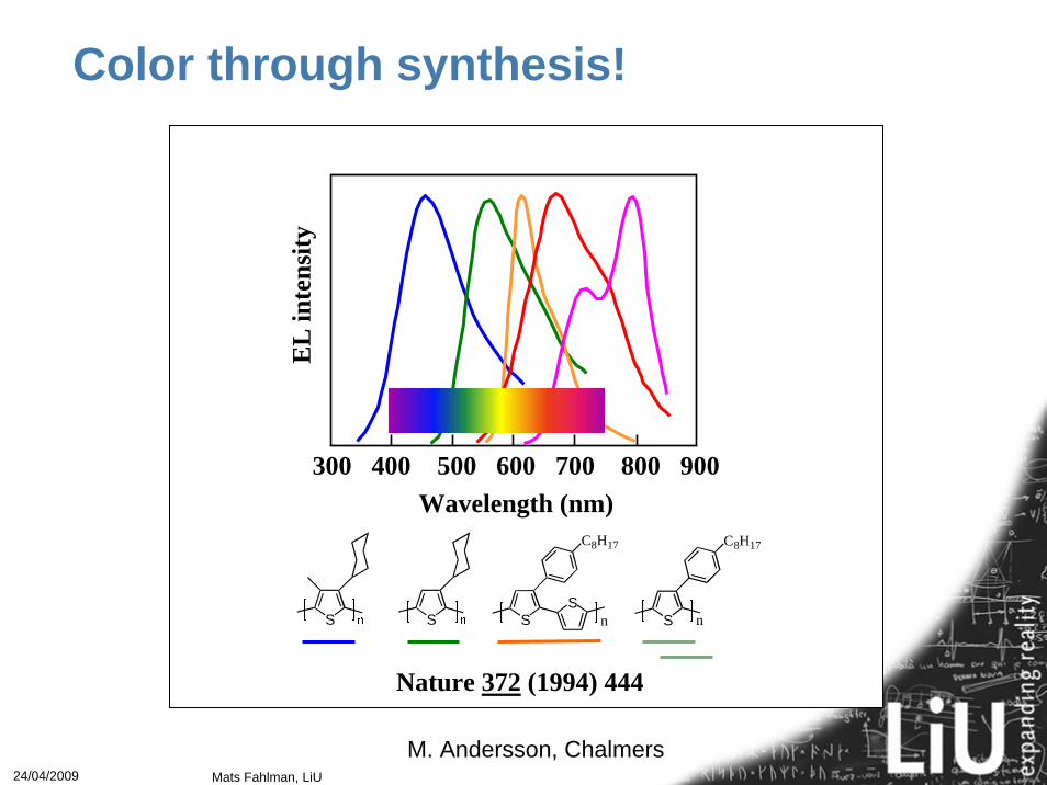
300 400 500 600 700 800 900Wavelength (nm)
SS
C8H17
S
C8H17
S S n n
Nature 372 (1994) 444
EL
inte
nsity
M. Andersson, Chalmers
Color through synthesis!

24/04/2009 Mats Fahlman, LiU
Circuits made by ink-jet printing (a disruptive technology)
PLEDs: example of an active-matrix display

24/04/2009 Mats Fahlman, LiU
Organic Electronics: flat screen TVs
Sony, Samsung, etc
http://www.youtube.com/watch?v=FAk4bjdbtCI

24/04/2009 Mats Fahlman, LiU
what is it?
Electronics
"1" "0"
read/write informationby charge pulses
Spintronics
"1" "0"
process information byselecting spin up/down
manipulate spin, measure a property that depends on spin
use spin directly, as in quantum computation
Spintronics

24/04/2009 Mats Fahlman, LiU
Magnetoresistance: change in resistance under an applied magnetic field
Can be positive or negative effect
Typically defined as ΔR=(R(B)-R(0))/R(0)Using “normal” mechanisms for magnetoresistance in materials, the π-conjugated molecules should have |ΔR|<10-6 at low magnetic fieldsHowever…
Magnetoresistance

24/04/2009 Mats Fahlman, LiU
Ö. Mermer,et al, PHYSICAL REVIEW B 72, 205202 2005
Organic Magnetoresistance (OMAR) effectSimple diode structureInsensitive to magnetic field (B) directionNon-magnetic electrodesNon-magnetic organic semiconductor|ΔR|~5-15% at RT!
Magnetoresistance in π-conjugated organic semiconductors (OMAR)

24/04/2009 Mats Fahlman, LiU
Some more peculiarities…
OMAR-effect changes sign depending on voltageOMAR also affects light emission: control light output by magnetic field
Ö. Mermer, et al, PHYSICAL REVIEW B 72, 205202 2005
Magnetoresistance in π-conjugated organic semiconductors (OMAR)

24/04/2009 Mats Fahlman, LiU
n: spin density at distance x from the ferromagnet/paramagnet interfacen0: spin density at distance x=0
e-e- barrier
e-Ferromagnetic half metal
Paramagnetic (semi)conductor
EF
FerromagneticHalf metal
ChangeMagnetization
”Valve” on/off!
Spin valve

24/04/2009 Mats Fahlman, LiU
“Designer magnets”, properties can be tuned by organic chemistry
Advantages:• Flexible• Low density• Potential low cost, low temperature synthesis• Variable electrical conductivity • Compatible with polymers and composites• Magneto-optic effects• …
Applications: SPIN elecTRONICS
Molecule-based magnets vs.Organic or hybrid organic/inorganic compounds• Active organic component (net spin in p-orbitals)• Passive organic component (no net spin)
Atom-based magnetsMetals or inorganic compounds withnet spin in d- or f-orbitals.
M(TCNE)x molecule-based magnets

24/04/2009 Mats Fahlman, LiU
1. existence of a magnetic moment (a net spin)
2. existence of magnetic interactions between spins
3. collective behavior ordering effect of interaction > disordering effect of thermalagitation
Ferromagnet
Below Tc Above Tc TTc
Paramagnet
“Ingredients” for magnetic ordering

24/04/2009 Mats Fahlman, LiU
M(TCNE)x, x~2, M=V, Mn, Fe…
M TC (K)
V 370
Fe 95
Mn 75
Co 40
Ni 40
V(TCNE)x: semiconductor, TC above room temperature
M. Gîrtu et al 1999-2000,C. Wynn et al 1998
J.M Manriquez, G.T Yee, R.S McLean, A.J Epstein, J.S Miller, Science, v252, 1991, 1415K.I Pokhodnya, A.J Epstein, J.S Miller, Adv. Mat., 2000, v12, 410
Tetracyanoethylene(TCNE)
[TCNE]– spin density distributionSchweizer, et al, JACS 116, 7243 (1994)
M(TCNE)x molecule-based magnets
24/04/2009 Mats Fahlman, LiU
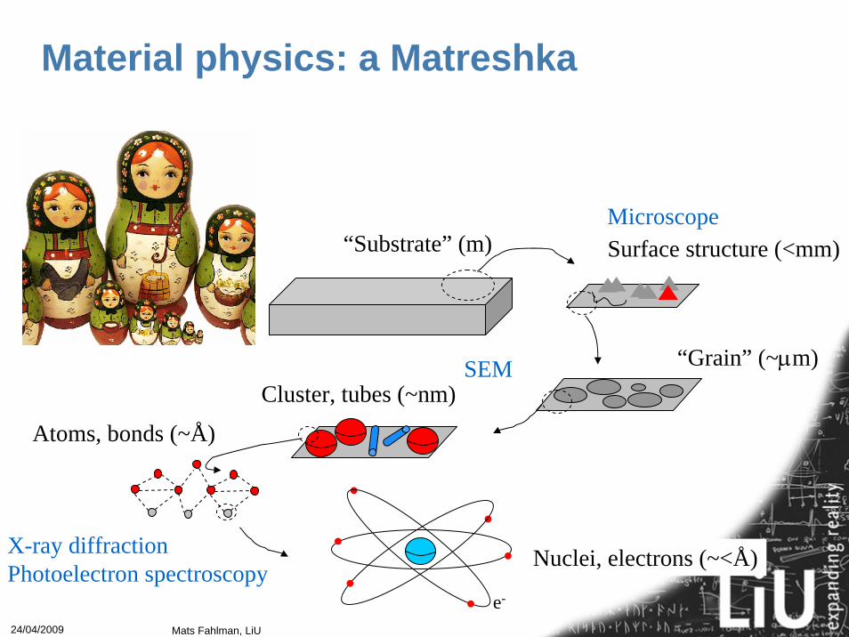
“Substrate” (m) Surface structure (<mm)
“Grain” (~μm)Cluster, tubes (~nm)
Atoms, bonds (~Å)
..
e-... . Nuclei, electrons (~<Å)
Microscope
SEM
X-ray diffractionPhotoelectron spectroscopy
Material physics: a Matreshka

24/04/2009 Mats Fahlman, LiU
ESRNMR
neutron scatteringpositron annihilation
FTIRIR
RamanHREELS
UV-Vis absorption
fluorescenceellipsometry
EELS
UPSIPES
NEXAFS EELSXES
XPSAuger
Scanning Tunneling Spectroscopy
TSC
phonons, magnons,
electronic excitation spin-excitations,core electron
excitationsnuclear
excitations
neutralspectroscopy:
ionizing spectroscopy:
transportspectroscopy:
Overview of spectroscopic techniques
24/04/2009 Mats Fahlman, LiU
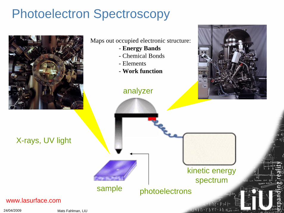
X-rays, UV light
photoelectrons
kinetic energy spectrum
sample
analyzer
www.lasurface.com
Maps out occupied electronic structure:- Energy Bands- Chemical Bonds- Elements- Work function
Photoelectron Spectroscopy
24/04/2009 Mats Fahlman, LiU
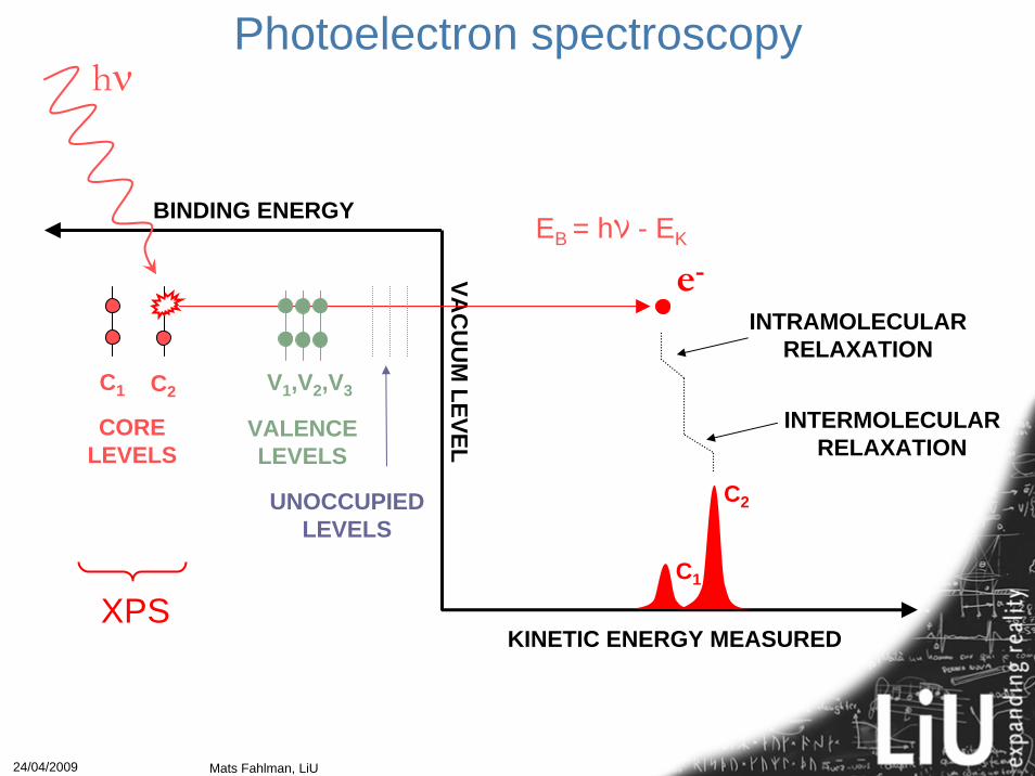
Photoelectron spectroscopy
KINETIC ENERGY MEASURED
BINDING ENERGY
VAC
UU
M LEVEL
INTRAMOLECULARRELAXATION
INTERMOLECULARRELAXATION
C2
C1
hν
EB = hν - EK
e-
C1 C2
CORELEVELS
VALENCE LEVELS
UNOCCUPIEDLEVELS
V1,V2,V3
XPS

24/04/2009 Mats Fahlman, LiU
Emission part
occupiedvalencelevels
core levels
Unoccupiedlevels
ground-state
photo-excitation
Spectator-decay
Participator-decay
Excitation partX-ray absorption event
X-ray absorption (NEXAFS) probes the unoccupied states in the presence of a core hole
Element and site specific method
It’s possible to obtain magnetic information using circular polarized light (XMCD)
X-ray absorption can be used to perform resonant PES…
X-ray absorption techniques

24/04/2009 Mats Fahlman, LiU
• Selectively deposits highly conductive polymer on dielectric resin and glass without the use of electroless copper. • Formaldehyde-free, environmentally sound technology. • Fast and uniform coverage of the plated through-hole. • Costly waste treatment and microetch post-treatments are not required.
Through-hole plating in Printed Circuit Boards

24/04/2009 Mats Fahlman, LiU
•Capacitors make up 90-99% of all components in most electronic devices• “Super” capacitors: Tantalum (Ta2O5) based (10-100 μF)• Traditional technology: use MnO2 as negative contact
• Problem – catches fire at high voltages!• Use Conducting polymer (PEDOT, Polyaniline) as cathode
• No fire risk• Significantly lower equivalent series resistance (ESR)
Capacitors

24/04/2009 Mats Fahlman, LiU
• Surface resistivity controllable between 10 and 106 ohm/sq• Volume conductivity ranges from 0.0001 to 5 S/cm• Can absorb up to ~90% of impinging microwave radiation • Dissipates static charge instantaneously regardless of humidityUses:EDS protection (clothes, carpets, etc)Microwave/radar absorptionResistive and microwave heating (clothes, blankets, etc)
Textile fibers can be individually coated with conducting polymers
Conductive textiles
24/04/2009 Mats Fahlman, LiU
• Conducting and semiconducting polymer films can anodically protect metals
• Can also act as on demand releasers of corrosion inhibitors
• Polyaniline typically used for steel and aluminum in construction, navy and aircrafts
Corrosion protection
24/04/2009 Mats Fahlman, LiU
Organic Electronics Research at LiU
Prof. Magnus Berggren, ITN, http://orgel.itn.liu.se/
Prof. Mats Fahlman, IFM, http://www.liu.se/ifm/surfphys/
Prof. Robert Forchheimer, ISY, http://www.bk.isy.liu.se/
Prof. Olle Inganäs, IFM, http://www2.ifm.liu.se/biorgel/
Prof. Sven Stafström, IFM, http:// cms.ifm.liu.se/theomod/compphys/


![Spintronics [EDocFind.com]](https://static.fdocuments.us/doc/165x107/577d2e0b1a28ab4e1eaea99b/spintronics-edocfindcom.jpg)