Permission to make digital orhard copies of all or part of ...
131
Copyright © 1990, by the author(s). All rights reserved. Permission to make digital or hard copies of all or part of this work for personal or classroom use is granted without fee provided that copies are not made or distributed for profit or commercial advantage and that copies bear this notice and the full citation on the first page. To copy otherwise, to republish, to post on servers or to redistribute to lists, requires prior specific permission.
Transcript of Permission to make digital orhard copies of all or part of ...

Copyright © 1990, by the author(s).All rights reserved.
Permission to make digital or hard copies of all or part of this work for personal orclassroom use is granted without fee provided that copies are not made or distributedfor profit or commercial advantage and that copies bear this notice and the full citation
on the first page. To copy otherwise, to republish, to post on servers or to redistribute tolists, requires prior specific permission.

HIGH SPEED CLOCK RECOVERY IN VLSI
USING HYBRID ANALOG/DIGITAL TECHNIQUES
by
Beomsup Kim
Memorandum No. UCB/ERL M90/50
6 June 1990

HIGH SPEED CLOCK RECOVERY IN VLSI
USING HYBRID ANALOG/DIGITAL TECHNIQUES
by
Beomsup Kim
Memorandum No. UCB/ERL M90/50
6 June 1989
ELECTRONICS RESEARCH LABORATORY
College of EngineeringUniversity of California, Berkeley
94720
-v

High Speed Clock Recovery in VLSI
Using Hybrid Analog/Digital Techniques
Ph.D. BeomsupKim Department ofEECS
Chairman of Committee
Abstract
The increasing popularity of high speed data transmission systems such as local area networks
(e.g. Ethernet, Token Ring etc.), disk drive systems, and optical communication systems (e.g. FDDI
etc.) alongwith constant evolution of betterIC technologies puts several stringent requirements on the
clock recovery circuits. Current implementations for these applications usually makeuse of an analog
PLL implemented in bipolar technologies, often using an emitter coupled multivibrator. These tech
niquesare limited in their ability to implement moresophisticated algorithms at high speed,and are not
well-suited to implementation in CMOS technology needed to achieve higher level of integration and
lower power dissipation.
The purpose of this research projectis to explore an alternative architecture whichovercomes the
limitations of the previous approaches and to investigate the circuit design issues associated with the
new architecture. Based on this research, the hybrid analog/digital clock recovery technique which
possesses the merits of analog PLL's and digital PLL's is of potential interest in high speed data
transmission and shows several advantages such as fast acquisition, low jitter, low error rate, and capa
bility of implementationof sophisticatedalgorithms.
A prototype chip was fabricated to evaluate the performance of the hybrid analog/digital clock
recovery circuit in 2jim CMOSprocess.This chip operates at a maximum data rate of 33 MHz from a
single 5-Vpowersupply andachieves veryfast phaseacquisition, a decode window of 94%of full win
dow width,effectivesamplingjitter of lOOps RMS,and an effective input samplingrate of 1 GHz. The
ring oscillator in the analog PLL showsa 62 ppm/deg C temperature coefficient (TC) and 4.5% supply
sensitivityof free-running frequency. The total power dissipation is about 600 mW and the active area
is 30,000 mil2 (20 mm2 in a2\im single-poly double-metal n-well CMOS process.

ACKNOWLEDGEMENT
I would like to express my deepest appreciations to the thoughtful guidance and
the continuous support that I have been privileged to receive from my advisor, Profes
sor Paul R. Gray. His advice is always valuable. I also would like to thank Professor
Rober R. Meyer for his help and suggestionson this thesis.
The exchange of ideas with fellow students at UC Berkeley is particularly fruit
ful. Among them, Yui-Min Lin, Cormac Conroy, Gani Jusuf, Greg Uehara, David
Helman, Steve Lewis, Sehat Sutarja come into mind. David Helman designed and
layed out l|im version of the chip and Ken Lutz provided me his assistance in the lab
set up and PC board design.
Special thanks goes to Cormac Conroy for his continuous proofreading this
thesis and many valuable suggestions. I would also like to thank Yiu-Min Lin for
sharing many fruitful discussion with me. To all of the IC group students I have
worked with, I appreciate all the help.
Finally, I dedicate this thesis to my dear wife Seung Hee Choi. Her love,
endurance and sacrifice she has been filling me with every single day in the monotoni-
city of the Albany village life enable me to finish my work. Also, I thank my and my
wife's family for their encouragement and support.
This research is sponsored by the National Science Foundation under grant
MIP-8801013, California MICRO program, Level One Communication, Xerox Cor
poration, and Texas Instruments. Prototype fabrication was done by MOSIS.

Table of Contents
Chapter 1 - Introduction 1
1.1 Background and Motivation 1
1.2 Thesis Organization 2
Chapter 2 - Clock Recovery in Digital Communication Systems 3
2.1 Introduction 3
2.2 Functional Objectives of Clock Recovery Systems 3
2.3 Clock Recovery System Performance Parameters 5
2.3.1 Input Characteristics 5
2.3.1.1 Line Coding 5
2.3.1.2 Intersymbol Interference 7
2.3.1.3 Input Phase Jitter 8
2.3.2 System Performance Parameters 10
2.3.2.1 Clock Phase Jitter 10
2.3.2.2 Acquisition Speed 11
2.3.2.3 Static Phase Offset and Stability 12
Chapter 3 - Clock Recovery Architecture Review and Comparison 14
3.1 Introduction , 14
3.2 Open Loop Clock Recovery Techniques 15
3.2.1 Spectral Line Methods 15
3.3 Closed Loop Clock Recovery Techniques 17
3.3.1 Continuous-Time Clock Recovery Methods 18
3.3.1.1 Early-Late Methods 18
3.3.1.2 Transition-Detection Based Methods 21
3.3.2 Discrete-Time Clock Recovery Methods 24
3.3.2.1 MMSE Clock Recovery Methods 25
3.3.2.2 Baud-Rate Clock Recovery Methods 26
3.4 Comparison of Clock Recovery Techniques 27
Chapter 4 - Hybrid Analog/Digital PLL 29
4.1 Overview 29
4.2 Architecture 32
4.2.1 Analog Phase-Locked Loop 34
4.2.2 Parallel Phase Sampler 39

-2
4.2.3 Transition Detector and Digital Phase-Locked Loop 404.2.4 Characteristics of Hybrid Analog/Digital Clock Recovery
46
4.3 Circuit Design Issues 484.3.1 Differential Delay Cell 494.3.2 Replica Biasing Circuit 514.3.3 Harmonic Oscillation 53
4.3.4 Dual-Latch Data Path 55
4.3.5 Pipelining in Digital Phase-Locked Loop 564.3.6 Phase Quantization Effects 60
4.4 Design of Hybrid Clock Recovery Circuit 614.4.1 Summary of Circuit Design Issues 614.4.2 Possible Extensions for Increased Performance ..: 62
4.4.3 Projected Performance in Scaled Technologies 63Chapter 5 - Jitter Analysis 66
5.1 Introduction 66
5.2 Jitter in RingOscillator 675.2.1 Fast-Slewing Saturated Ring Oscillator 695.2.2 Slow-Slewing Saturated RingOscillator 745.2.3 Non-Saturated RingOscillator 795.2.4 Comparison of Ring Oscillator Jitter Performances 81
5.3 PLL Phase Noise Accumulation 82
5.4 DLL Phase Jitter 86
5.5 Example: PLL Noise Analysis with Slow-Slewing Saturated RingOscillator 89
5.6 PLL Phase Jitter System Simulation 96Chapter 6 - Optimal K Sequence for the DPLL 100
6.1 Introduction 100
6.2 Problem Definition 100
6.3 Optimization Based on Minimum Mean Square Criterion 1036.4 Optimization Basedon Minimum Mean Sum of Squares Criterion
105
Chapter 7 - Experimental Results Ill
7.1 Introduction Ill
7.2 Analog PLL and Parallel Phase Sampler Ill7.3 Hybrid Analog/Digital Clock Recovery 115
Chapter 8 - Conclusion 120

8.1 Summary of Research Results 120
References 121

Chapter 1
Introduction
1.1 Background and Motivation
In modem data transmission systems such as local area networks, disk drive sys
tems, telecommunication networks, and optical communication systems, information
is transmitted or received in the form of either baseband or passband signals contain
ing sequences of digital data symbols. In these applications, usually only data signals
are transmitted by the transmitter and separate clock signals used to synchronize the
data are not transmitted to save the expense of interconnection and hardware. There
fore, the receiver should incorporate a circuit block, called the clockrecovery circuit,
to recover the clock information from the received data, and synchronize the data with
the recovered clock.
Since the demands of the data transmission system grow fast, many alternatives
are studied to achieve high performance clock recovery circuits for several different
applications ranging from relativelyslowdigital subscriber loops to high speed optical
data communications. One of the most challenging areas for the clock recovery cir
cuits is high speed data transmission applications such as the disk drive read channel,
the local area networks (Ethernet, Token Ring etc.), and optical communications
(FDDIetc).
In these applications, clock recovery from received data must be performed with
stringent requirements on small static phase offset, low sensitivity of decode error to
phase jitter, and various programming capabilities. Currently most high speed clock
recovery circuits make use of an analog PLL implemented usually in bipolar technol
ogy, using either an emitter coupled multivibrator or a starved ring oscillator

VCO,[H.LEE] and utilize techniques such as zero-phase start and PLL time constant
gear-shifting to achieve fast acquisition at the start of preamble. But these techniques
are limited in their ability to implement more sophisticated algorithms at high speed,
and also are not well-suited to the CMOS implementation needed to achieve higher
levels of integration and lower power dissipation in high speeddata transmission sys
tems.
This dissertation describes a new architecture based on an analog PLL and a
digital PLL, namely the hybrid analog/digital clock recovery circuit, which was
developed to allow the use of CMOS technology to achieve high speed datarecovery,
fast phase acquisition andlarge input jitter tolerance and also allowimplementation of
sophisticated algorithms at high speed such as digital zero-phase start, digital gear-
shifting, programmable window width/offset, and programmable pulse pair compen
sation. The large phase jumps normally associated with digital PLL's are avoided.
1.2 Thesis Organization
Chapter 2 introduces the functional objectives of clock recovery systems and
their performance issues. In Chapter 3, several conventional clock recovery methods
arereviewed and compared. Chapter 4 describes the overall architecture of the hybrid
analog/digital clock recovery system, investigates the circuit design issues and
addresses their solutions. One of key performance issues, PLL jitter, is studied in
depth in chapter 5. Chapter 6 derives the optimal solution of the digital PLL control
parameter sequences based on a minimum mean square error criterion. In chapter7,
experimental results from the 2|im CMOS prototype hybrid analog/digital clock
recovery circuit are presented. Finally, chapter 8 gives a summary of the research
results and conclusions.

Chapter 2
Clock Recovery in Digital Communication Systems
2.1 Introduction
In this chapter, firstly, the objectives of clock recovery circuits are introduced.
Next, the problems and the performance issues related to clock recovery circuits are
reviewed. This chapter forms the basis for the following chapters.
2.2 Functional Objectives of Clock Recovery Systems
In most data transmission applications in local area networks, disk drive systems,
telecommunications and optical communications, information is transmitted or
received in the form of either modulated or unmodulated sequences of digital data
bits. In these applications, usually onlydata signals are transmitted by the transmitter
and separate clocksignals are not transmitted in order to savethe expense of intercon
nect and system hardware. Therefore, the receiver should incorporate somecircuits to
recover the clocksignals from the received datasignals, andsynchronize the data with
the recovered clock. These circuits are usually called clock recovery circuits or tim
ing recovery circuits.
Figure 2.1 shows the clock recovery function. Here the clock recovery circuit
takes the data bit stream and generates clock pulses with rising edges in the center of
each received data bit The data decision circuit synchronizes the data bit stream
using the rising edge of the recovered clock pulses. Since initially, the receiver does
not know the phase and the frequency of the incoming data pulses, the clock recovery
circuit needs a time period, called the preamble period, to acquire the phase and fre
quency. Also, in steady state, the clock recovery circuit must maintain the frequency

and phase locking in the presence of input jitter and missing pulses ( data "0u,s). In
the following sections, these issues are explained in detail.
Bit StreamClock Recovery Circuit
Bit StreamA
Recovered ClockA
Synchronized DataA
Data Decision Circuit
Synchronized Data
Figure 2.1 Function of Clock Recovery Circuits
Figure 2.2 shows the block diagram of typical data transmission receiver with a
clock recovery circuit Here, the preamp circuit detects the low level electric signals
from the communication channel (e.g disk drive heads, coaxial cables, and twisted
pair wires), and amplifies them. The following AGC circuit amplifies the outputs of
the preamp circuit to a proper voltage level. The equalization filter reshapes the signal
degraded by the communication channel to the original pulse shape. The pulses com
ing from the equalization filter are used to derive clock information and synchronize
the data with the recovered clock signals generated from the clock recovery circuit.
Currently, most high speed clock recovery circuits make use of an analog PLL

implemented in bipolar technology. But to achieve higher level of integration and
lower power dissipation for future data transmission receiver applications, the use of
CMOS technology is preferred.
From_Channel
PreampV
AGC*. Filter
Decision
CircuitController
1*T
/ hClock Recovery
Circuit
.1111 » 'a, , ; , /v
tor i i iJ• •••I
n in : in,.i i i i i i
To
Host
Figure 2.2Typical Data Transmission System Receiver
2.3 Clock Recovery System Performance Parameters
In this section, some of the important performance parameters of clockrecovery
circuits are presented. The subject is divided into two parts; (i) problems associated
with the input signal source, (ii) systemlevel issues.
2.3.1 Input Characteristics
In this section, various line coding methods for the input signal are described,
and the intersymbol interference and the phase jitter associated with the input signal
are discussed.
. 2.3.1.1 Line Coding
Line coding techniques have been extensively studied since the emergence of
local area networks and the ongoing evolution of the telecommunication network to
digital service. Line coding is usually used inbroadband communication systems such

as baseband local area networks (Ethernet, token ring, optical networks and so forth),
disk drive read and write channel, and short loop digital PBX connections for termi
nals, hosts, and digital phones. In such systems, the transmission media cause only
moderate distortion of the pulse because the bandwidth of the channel is wider than
the spectrum of the signals. The important requirements of the line coding are spec
tral shaping, reduction ofdc wander, bandwidth efficiency, and signal synchronization
capabilities.
The easiest way to shape the spectrum of the transmitted signal in a binary sig
naling scheme is a suitable choice of the signal waveforms. Figure 2.3 shows the sig
nal waveforms for nonreturn-to-zero (NRZ) code, return-to-zero (RZ) code, Man
chester (or biphase) code, and Miller (or delay modulation) code scheme.
RZ
NRZ
1•\ j o j 0•
j !!
1
i o ! o |i ij :
1 i
0'
i o | 0 |
i!:
| j j
i
1t
] i
i
\r
1
•
i•
j
i
j
s !$
Manchester
Miller
Figure 2.3 Pulse Shapes of Various Line Coding Schemes

NRZ is the simplest code, it also makes efficient use of bandwidth. The main
limitations of NRZ are the presence of a dc component and the lack of synchroniza
tion capability. RZ is basically the same as NRZ except it occupies more bandwidth.
Manchester code uses more bandwidth to ensure a predictable transition in themiddle
of each interval to remove the dc component. Also the receiver can use this informa
tion for clock recovery and error detection. In the case of Miller code the code can be
represented through a modulation with memory to deliberately achieve a higher
bandwidthefficiency and the minimum dc component
2.3.1.2 Intersymbol Interference
Even in broadband transmission, dispersion causes degradation of the pulse,
called intersymbol interference (ISI). For example as shown in figure 2.4, in the case
where the transmission line can be represented by a simple RC network, the transmit
ted signals experience trailing type dispersion and the shapes are degraded.
Bit SignalCoder Hardware
01010
Coded Signal A . . Transmission Line"Wlr-
"5"
Figure 2.4 Signal Degradation Caused by Dispersion
To quantify the degradation of the signal, a graphical illustration called an eye
diagram is used. Figure 2.5 shows the eyediagrams for the ideal pulse and degraded
pulse. In an eye diagram, as thedegradation gets worse, thecenter of theeye becomes
narrower and the probability of transmission error increases. For a channel with lim
itedbandwidth, since the signal degradation is very severe, pulse shaping often using

8
Nyquist pulses [LEE], is required to reduce the intersymbol interference. In broad
band transmission systems, while the intersymbol interference is not as severe, jitter
caused by signal noise on the degraded pulses is the major obstacles to error-free
transmission.
a. Ideal Pulse b. Degraded Pulse
-1/2T 1/2T -1/2T 1/2T
c. Eye Diagram for the Ideal Pulse d. Eye Diagram for the Degraded Pulse
Figure 2.5 Effect of Pulse Degradation on Eye Diagram
2.3.1.3 Input Phase Jitter
The received signal always contains noise generated from a number of noise
sources such as thermal noise, crosstalk, shotnoise and so forth. The noise affects the
shape of signals and pulse position. In general, an ideal clock recovery circuit takes a
sequence of time positions at which a rising or falling edge of a pulse crosses some
threshold voltage and averages the time positions to derive the real input pulse posi
tion. This averaging process makes the clock recovery circuit insensitive to position
variation of the edge for input signal edges, referred to as jitter. However there is a
limited amount of input jitter that a real clock recovery circuit can tolerate. Therefore
insensitivity toinput jitter is a very critical requirement for clock recovery circuits and

decision circuits. Figure 2.6 shows the input jitter and eye diagrams when the input
signal has jitter.
Data *
Clock *
(a) Input Jitter Caused by Noise
Data A
t
Sampling Position
Clock *
(b) No Jitter In Clock
lit
X' *
'' •ILTJUm^'t
Sampling Position
nn •
•>
(c) Jitter In Clock
Figure 2.6 Input Jitter and Eye Diagram
Here in the figure 2.6.(a), the time position of rising edge crossing the threshold
voltage is shifted to the left from the ideal position because the noise changes the vol
tage near the threshold voltage. Also the center opening of the eye diagram is nar
rower as the noise gets worse (figure 2.6.(b)). This indicates that the probability of

10
data transmission error increases because the signal-to-noise ratio decreases with nar
rowing of the eye opening. Note that here the clock is assumed to have no jitter. In areal situation, clock recovery circuits generate clocks containing some jitter. There
fore the sampling point also moves around the center of the eye and the error probabil
ity alsoincreases (figure 2.6.(c)).
2.3.2 System Performance Parameters
In this section, the problems of clock recovery circuits are described. The first
sub-section discusses clock jitter, the second deals with acquisition speed, and the last
one describes static phaseoffsetand stability.
2.3.2.1 Clock Phase Jitter
Similar to the input signals, clock signals also contain jitter caused by several
noise sources such as thermal noise, shot noise, power supply noise, input jitter and so
forth. As shown previously in figure 2.6, if the clock signal has jitter, the sampling
moment of the data is wandering which results in large data transmission errors
through the channel. This phenomenon gets worse as the clock edge moves further
away from the center of the eye. Here, one bit interval (from the figure, one pulse
interval) is called a decoding window. The jitter aspect ofthe performance of clock
recovery circuits can be characterized by the bit error rate as a function of decoding
window as shown in figure 2.7.

Data
Clock
Decoding Window
K *
Input Jitter
f:kJClock Jitter
Bit Error Rate
4
1
1<f
Maximum Effective j
ecodlng Window< W
11
50% 100%
Decoding Window
Figure 2.7 Bit Error Rate vs Decoding Window
In the vicinity of the wall of the decoding window, the bit errorrate (the proba
bility of false decision ) approaches 1, and in the center region of the decoding win
dow, the bit error rate is minimum. Here the distance between two crossing points
with the some probability threshold is defined as the maximum effective decoding
window . In typical disk drive applications, a window width of 90% or more is
required at the 10 bit error rate. In digital transmission channels, the threshold is
usually 10"8, but asmaller window width is allowed because of smaller input jitter.
2.3.2.2 Acquisition Speed
In most data transmission channels, the clock information should be derived
from the incoming data bit stream. When the clock recovery circuit begins reading a
new data record, the clock recoverycircuit does not know the frequency and the phase
of the incoming data bit stream. Therefore, it is necessary to have some "grace period"
to acquire the phase and the frequency and to synchronize the data. For this period,
called preamble period, the transmitter usually send some regular sequence of pulses,
for example 101010..., in order to help the clockrecovery circuit acquire the phase

12
and frequency ofthe pulses. This signal pattern is called apreamble sequence. Figure
2.8 shows the preamble sequence and the clock synchronization. The acquisition
speed of the clock recovery circuit determines the length of the preamble sequence to
be sent by the transmitter. Therefore to reduce the time spent for this preambling, the
clock recovery circuit should be capable of fast acquisition.
Input
Clocks ^ Moving BackwardSampling
Figure 2.8 Definition of Acquisition Speed
2.3.2.3 Static Phase Offset and Stability
Due to circuit non-ideality and offset, the derived clock does not have its rising
edge in the center of the eye but is shifted to the right or left alittle bit This shift is
called static phase offset and represents another source of data transmission error.
Therefore this static phase offset should be small enough. Figure 2.9 shows the static
phase offset
High performance clock recovery circuits usually incorporate a phase-locked
loop. The loop may beunstable if acertain stability criteria are not met (this will be
described in detail in later chapters) because the loop can be thought of as a negative
feedback loop. If the loop is not stable, the position of the clock signal will oscillate
and the PLL will fail to acquire the phase and the frequency of the incoming data bit

13
stream. Thus, stability consideration of the clock recovery circuit isanother important
factor to achieve a high performance system.
Data >
Static Phase Offset
IT\ \
\ 1i
L : *•
Clock' <
>
Figure 2.9 Static Phase Offset

14
Chapter 3
Clock Recovery Architecture Review andComparison
3.1 Introduction
Clock recovery techniques have been studied since the appearance of data com
munications. Many ideas have been suggested to implement clock recovery circuits
for several different applications. In general, clock recovery techniques can be divided
into two broad classes depending on the application. The first category is open loop
clock recovery, in which the incoming signal is passed through anonlinear device and
a frequency shaping circuit, and the resulting signal is used to sample the incoming
signal to extract the carried information. This method does not have a feedback loop,
therefore, it is simple and is used in high frequency clock recovery applications. The
spectral line method is an example ofopen loop clock recovery. The second class of
the techniques is closed loop clock recovery with a feedback loop, in which symbol
timing error is estimated and the error is fed back to a voltage controlled oscillator
(VCO). The VCO is then controlled to adjust the sampling instant to the middle of the
symbol interval.
The closed loop clock recovery method is characterized by several factors; one
of the principal factors being the method used to determine the phase error. On this
basis, closed loop clock recovery techniques may be divided into two further
categories. The first one may be referred to as continuous-time clock recovery, and
the second discrete-time clock recovery. Thecontinuous-time clockrecovery method
generates continuous-time phase error signals from a multiplier orsome logic circuits,
and these signals are direcdy used to control a VCO. Li contrast, the discrete-time
clock recovery technique samples the input signals with a VCO clock creating phase

15
errors in the discrete-time domain, and controls the VCO after doing subsequent sig
nal processing in the discrete-time domain. Continuous-time clock recovery circuits
are usually used in broadband data communication systems such as local area net
works (e.g. Ethernet, Token Rings), optical communication networks, and disk drive
read channels which do not suffer large signal degradation. Discrete-time clock
recovery is used in low speed applications for band-limited data communication sys
tems through telephone lines or narrow-band communication channels. Examples of
the latter are digital subscriber loops and integrated services digital networks (ISDN).
In this chapter, closed loop clock recovery techniques are emphasized. Open
loop clock recovery techniques are treated, briefly in section 3.2. Section 3.3
describes closed loop clock recovery techniques. Finally, in section 3.4, some com
parisons among these techniques arepresented.
3.2 Open Loop Clock Recovery Techniques
There are not many distinct open loop clock recovery techniques since the per
formance is relatively poor compared toclosed loop clock recovery circuits. However,
for very high frequency applications, this method is frequendy used because of its
simplicity.
3.2.1 Spectral Line Methods
One of the oldest methods, still used in microwave frequency range clock
recovery, is the class of spectral line methods. This method is the simplest method of
overall clock recovery and based on the clock tone present in the power spectrum of
the incoming data bit stream.
We assume that the digital information is transmitted by weighted pulses, each
with identical shape and spaced uniformly by T sees. If the impulse response of each

16
pulse is represented by p(t\ then the incoming baseband data pulse stream may be
represented as
R(ty=fAkp(t-kT) (2.1)
where A* are the transmitted symbols. In binary transmission scheme, A* can be
either "-1" or"1". When the mean-value of the data symbol is non-zero, thebaseband
pulse stream contain aspectral line at the baud rate. To determine whether aspectral
line at the baud rate exists from the data pulse stream, R(r) can berepresented by the
following equation.
R(t)=E[Ak] £ p(r-m7> £ (Am-E[Ak])p(t-mT) (2.2)m=-» in
The first term isindependent of the data A*, isperiodic with period T, and can be
thought of as adeterministic signal. Its periodicity implies afundamental at the baud
rate" 2%/T. This fundamental frequency can be extracted with a bandpass filter. The
second term is zero-mean and random, and results in jitter on the recovered clock
tone. This method is called linear spectral line method. However, in most case, the
mean-value of data symbols is zero, there isno strong clock tone in the incoming data
bit stream. But often the second and higher moments of the incoming signal are non
zero and periodic. Therefore, to derive aclock tone, the incoming signal is passed by a
nonlinear component (such as squarer) and filtered by a bandpass filter. These
methods are called nonlinear spectral line methods . To illustrate this, a squarer dev
ice is used as an example. If the correlation function of the data symbols is expressed
as (2.3),
£[AmAn]=al8m.n (2.3)
the expected value of the output of the squarer device can be expressed as (2.4).
E[R (f )2]=oi £ p(t-mT? (2.4)

17
This expectation value can be considered a deterministic component of the output of
squarer device and it isperiodic with period T. The fundamental ofthis signal will be
extracted by the bandpass filter. Figure 3.1 shows the block diagram ofthis approach.
Bit Stream Nonlinear
Device(Squarer)Bandpass Filter
Clock
Figure 3.1 Nonlinear Spectral Line Method
The primary advantage of this approach is in its simplicity. Since it does not
require any complex circuitry inside, it can be used in high speed clock recovery cir
cuits. In microwave frequency range clock recovery, this method can be easily imple
mented by nonlinear device and a bandpass filter. However, since the passband of the
bandpass filter is not usually realized accurately enough, the noise rejection is some
times poor, therefore the phase jitter, caused by this noise is usually considerable.
Also, the entire clock recovery depends on thesimple bandpass filter: there is no good
way to control the static phase offset and the acquisition time. As a result, it require a
long preamble period and displays large phase errors due to the nonlinear device and
the bandpass filter.
3.3 Closed Loop Clock Recovery Techniques
As mentioned, the closed loop clock recovery methods are dividedinto two categories
based on how phase errors are processed. Section 3.3.1 describes continuous-time
clock recovery techniques, and section 3.3.2 explains discrete-time clock recovery
techniques.

18
3.3.1 Continuous-Time Clock Recovery Methods
Almost all clock recovery circuits in this category use a PLL. Based ondifferent
PLL topologies, several approaches are presented. Here, two examples, early-late
methods, and transition-detection based methods are illustrated in section 3.3.1.1 and
3.3.12 respectively.
3.3.1.1 Early-Late Methods
Early-late method is very popular for several broadband transmission applica
tions. Figure 3.2 shows the block diagram for an example. In this diagram, the input
signal is integrated by a pair of gated integrators, each performing its integration over
a time interval of 772. Integration by the early gate occurs in the 772 preceding the
nominal location of data transitions and the output is held by thefollowing sample and
hold circuit for the next 772. While the late gate integrates during the 7/2 immedi
ately following the transitions and the following sample and hold circuits hold the out
put for the next 772. If timing error is zero, the data transitions fall exacdy on the
boundary between early and late gates.
Input
Early
Integrator
Odd Clock
Even Clock
Late
Integrator
Sample &
Hold
VCO
Sample &
Hold
Figure 3.2 Early-Late Method
LPFVe

19
If the input leads the VCO clock, the rectified output of early gate sample and
hold circuits will generate smaller voltage than that of late gate sample and hold cir
cuits. Therefore the lowpass filtered output of the error voltage will increase and the
VCO clock will go faster and in phase. Figure 3.3 shows the waveforms for this case.
InputA
VCO ClockA
> t
Early ntegrate and Hold
Late Integrate and HoldA
Late Hold|- Early Hold|> w
A\ erage Level** **
Figure 3.3 Clock Waveforms for Early-Late Method
> t

20
In figure 3.3, the VCO clock rising edge lags behind that of the input signal. The
early gate integrates the input signal for the early-half period of the clock signal, and
holds it for the remainder of the clock period. On the other hand, the late gate
integrates the input signal for the late-half period ofthe clock signal and hold it for the
next early-half period. If the absolute values ofthe late gate hold signals are taken for
the early-half period of the clock signals, and the negative of the absolute values of
the late gate hold signals are taken for the late-half period of the clock signals, the
resultant signals are represented by figure 3.3. The averaged value of these signals
generated from alowpass filter gives the control signal to adjust the phase of the VCO
clock signals.
As a summary, when the transition occurs, the output of each rectified sample
and hold circuit shows the different voltage level. For some time, these differences
are accumulated through the lowpass filter which results in shifting of VCO clock
pulse to the left by increasing the frequency of VCO. But if no transition occurs, no
voltage difference is generated from the subtracter, therefore there will be no change
of the VCO frequency. Basically, this technique can be used innarrowband transmis
sion systems if the integrators are removed. But it requires 2 X higher sampling than
baud-rate sampling techniques which are widely used innarrowband transmission sys
tems.
As mentioned earlier, this method is popular for rectangular pulses. Since this
method relies on the shape of the pulses, a large static phase offset can beintroduced
if the pulse shape is not symmetric. Inhigh speed applications, the twointegrators are
required to settle very fast, which limits the operating speed of the clock recovery cir
cuit Also the acquisition time is not easilycontrolled.

21
3.3.1.2 Transition-Detection Based Methods
The most widely used technique for clock recovery in high performance wide
band data transmission application is the transition-detection based method. There
are many variations of these methods depending on the exact implementation of each
PLL loop component However, the basic configuration is the same for almost all
implementations andshown in figure 3.4.
Bit Stream. Transition
Detector.
V n >> LPF——fp ru p
a
•
J k
VCO
Clc>ck
*\
Figure 3.4 Transition-Detection Based Clock Recovery Method
Usually, the input is transmitted using NRZ line coding. Since the NRZ signal
does not have a frequency component at the baud rate, it is necessary to change the
NRZ signal to another form of signal which has a frequency component at the baud
rate. The transition detector in figure 3.4 does this function. It detects the transition
edge and generates apulse corresponding to the transition edge (both low-to-high and
high-to-low transition ). In effect, it translates the NRZ signal to RZ signal which has
a strong frequency component at the baud rate. Then, the phase detector compares the
RZ signals with the VCO clocks. For example, a simple multiplier can be used as a
phase detector. In this case, the VCO clock is shifted by 90 degrees to the left when
the phase detector generates output signals with the zero dc components ( when the

22
PLL is locked into input signal). If the VCO clock is shifted by more than 90 degree
to the left, the output signals with a negative dc component are generated from the
phase detector and the VCO clock is adjusted to the right The lowpass filter extracts
the dc component from the phase detector output Rgure 3.5 shows the output
waveforms of each block.
This method has many merits. First, there isno slow circuit in the loop, therefore
it can beused for high speed clock recovery. Also, since the clock recovery circuit can
use the pulse transition edge to derive the clock information without relying on the
pulse shape, static phase offset can be reduced. However, the static phase offset still
depends on the precision matching on the loop components and the path delays. Also,
fast phase acquisition requires complex analog design and many external components.
Conventional digital PLL's can solve those problems, however these are not practi
cally usable because of large phase jumps normally associated with them. Currendy,
many clock recovery circuits for the high performance applications are built using
analog PLL based method with zero-phase start and gearshifting techniques.

Input NRZA
RZA
VCO Clock In PhaseA
PD Output (Zero DC)A
Fast VCO ClockA
PD Output (Negative DC)A Negative DC
u
Figure 3.5 VCO Clock and Phase DetectorOutput Waveforms
23
-» t
* t
* t
-> t

24
3.3.2 Discrete-Time Clock Recovery Methods
In narrowband data, transmission system such as a digital subscriber loop through
a telephone line, the received data waveforms are degraded very much due to pulse
dispersion, noise and echo. Therefore, sophisticated signal.processing is involved and
it is not feasible to use the simple clock recovery circuits describes earlier in section
and 3.2 and 3.3.1. For example, in the full-duplex digital subscriber loop transceiver
shown figure 3.6, the clock recovery circuit does not take the incoming data direcdy,
but takes it after receive filter, sampler and echo canceler. Thus the signal being sam
pled isnot the square pulse that is usually available in the broadband transmission sys
tem, but dispersed pulses ( if ideal, Nyquist pulses ). The minimum mean-square
error (MMSE) and the baud-rate sampling techniques are the good candidates for
such system.
TX Data
Scrambler
Descrambler Detector
REC Data
Echo
Canceler
Line
Coder
Sampler
Clock
Recovery'Clock
Transmitt
Filter
Hybrid
Receive
Filter
Figure 3.6 A Full-Duplex Digital Subscriber Loop Transceiver
Line

25
3.3.2.1 MMSE Clock Recovery
In figure 3.7, the received signal is sampled at times £T+r*. Here, the symbol
interval is T, and the timing error is represented by zk. If the output of the receive
front end filter is Qk(xk) , and the correct data symbol is Ak , the MMSE clock
recovery circuit adjusts ik to miriimize the expected square error between the input to
the slicer and the correct symbol,
E[\Ek{Xk)\^=E[\Qk{!kyAk\*\ (3.5)
Since the input to the slicer Qk(xk) is acomplicated nonlinear function of the timing
phase tk, the expected squared error is minimized by adjusting the timing phase in the
direction opposite the derivative of the expected value of the squared error. Then the
new timing phase is
dQhdk)xk+i=*k-a&e Ei<?kY ~5%i(3.6)
To realize the derivative function using the discrete-time filter, the derivative is
approximated by (3.7).
^^-=(2^i^)-fi.-i(^))/r (3i7)
Then, (3.6) becomes (3.8).
^+i=tjfe-a'Re {Qktok)-^k]lQk+itokhQk-i(W] (3.8)
where the a' is -2- and the Ak is the slicer output replacing the actual symbol Ak in the
decision-directed tracking period. In the training period, the actual known symbols
Ak are available and are used to aid phase acquisition.
One problem of this method is that since Ek(xk) is not linear function of xk, the
stochastic algorithm on which this method relys is not guaranteed to converge to the

26
optimal timing phase. Therefore, in practice, some other techniques should be used in
the acquisition time to get reasonably good timing phase. Also, this method requires
Nyquist sampling which is 2 X higher than the baud-rate sampling because of the
discrete-time differentiator realization. The next clock recovery circuit, baud-rate
sampling techniques allow baud-rate sampling.
kT+zk
SlicerAk
Ak
Timing Error
Estimator
Figure 3.7 MMSE Clock Recovery Techniques
3.3.2.2 Baud-Rate Clock Recovery
There are several baud-rate clock recovery techniques using discrete-time clock
recovery methods. One of the techniques derived from MMSE techniques are as fol
lows. If the timing function to update thetiming phase is defined as (3.9).
/(x*)=-Re E\Qk(*k>-Ak]\Qk+i(ik)-Qk-i(!k)] (3.9)
Then, f(xk) becomes (3.10) under the assumption that Qk(tk) is a wide sense

stationary (WSS) random process.
/(T*)=Rej E[AkQk+l(xk)]-E [AkQk-i(ik)]For example, if the continuous time PAM signal at time £T+T* is(3.11).
Qktok> t Amp((k^m)T^ik}+Nk (3.11)m
27
(3.10)
where the Ak and Nk are WSS random processes and Nk is zero mean and indepen
dentofAk.Then, the timing function is (3.12).
ftey&llAtWlplXk+Typto-T)]. (3.12)
If p(t) is symmetric about xk, the timing function will be zero at/ (0)=0.
This method is very attractive for the narrowband clock recovery circuits
because the nature of the baud-rate sampling helps the design of the echo canceler and
equalization filter which are commonly used in the digital subscriber loops.
3.4 Comparisonof Clock Recovery Techniques
In this section, qualitative comparisons among the clock recovery methods
described above are made based on applications and performance. First", the clock
recovery methods are divided into several categories. Then, application areas are
defined. Next, the clock recovery circuits are divided based on the operating speed,
acquisition speed, input jitter tolerance, complexity and some examples are given.
Table 3.1 summarized these. Here, SLM, ELM, TDM, MMSEM, and BRM represents
Spectral. Line Methods, Early-Late Method, Transition-Detection based Method,
Minimum-Mean Square Estimation Methods, and Baud-Rate clock recovery Method,
respectively.

28
Table 3.1 Comparison of Clock Recovery Methods
Name SLM ELM TDM MMSEM BRM
Method Open Closed Closed Closed Closed
Phase Error Continuos Continuous Continuous Discrete Discrete
Operating Range Broadband Broadband Broadband Narrowband Narrowband
Acquisition Speed Slow Slow Fast Slow Slow
Jitter Tolerance Low High High Low Low
Complexity Simple Simple Simple Complex Complex
Examples Microwave LAN LAN, Disk Modem, ISDN Modem, ISDN

29
Chapter 4
Hybrid Analog/Digital PLL
4.1 Overview
As mentioned earlier, many alternatives have been studied to achieve high per
formance clock recovery circuits for several different applications ranging from rela
tively slow digital subscriber loops to high speed optical data communications. How
ever, one of the most challenging areas for high speed clock recovery circuits is the
disk drive read channel for the following reasons.
1. When compared with other communication channels, the bit stream com
ing from the magnetic medium has large amount of jitter coming from
inter-track modulation, pulse dispersion, offset, and power supply and
thermal noise. Therefore, the circuit should tolerate large input jitter.
2. Since the preamble time for the disk drive increases the disk searching
time, the clock recovery circuit should possess fast acquisition time in
order to reduce the preamble time.
3. The data bit rate in the disk drive read channel is approximately from 15
MBits/sec to 60 MBits/sec. Therefore the clock recovery circuits should
operate at these high speed.
4. The high performance disk read channel requires several complex func
tional blocks which can handle such features as the multiple frequency
tracking, window shift and shrink, and pulse pair compensation etc.
which makes the design of the clockrecoverycircuit difficult
Figure 4.1 shows the typical disk drive read channel using a pulse detection
scheme. Here, the disk heads reads the data stored in magnetic medium through

30
magnetic flux changes and sends small electric signals to the preamplifier. The output
ofthe preamplifier is amplified through an AGC to aproper voltage level and filtered
by apulse slirnming filter. The peak detector detects the peaks of the signal and gen
erates pulses corresponding to these peaks. Then, the pulses coming from the peak
detector are used to derived the clock information and to detect data through a clock
recovery circuit called a data separator.
CLKREC+
ENC/DEC
CON
Data Separator
-15-30n»window
K-30-60MHZCfK
Figure 4.1 Typical Disk Drive Read Channel
There are several requirements for this data separator. When the disk drive
begins reading anew data record, the clock recovery circuit must align its local clock
with the incoming data bit stream as rapidly as possible. Techniques of zero phase
start and variable loop time constant are used to speed up the acquisition time, but
acquisition time of20-40 bit cycles is required for the current implementations. Since
the acquisition time is waste time, it is desirable to reduce it In steady state, the clock
recovery circuit must decode data correcdy in the presence of alarge amount of jitter

31
and other circuit impairments. Therefore, static phase offset should be reduced and the
decoding window width should be increased. For high performance disk drives such
as zonal disk, the disk drive is required to track multiple frequency data bit streams.
Also for system level tests and diagnostics for the disk drive system, the disk drive
mustbe able to incorporate variable programming capabilities.
Currendy most high speed data separators for disk drives make use of an analog
PLL implemented in bipolar technology using emitter coupled multivibrator or
starved ring oscillator VCO's. But these techniques are limited in their ability to
implement the above capabilities and more sophisticated fast-acquisition algorithms at
high speed, and also are not well-suited to CMOS implementation which isneeded to
achieve higher levels of integration and lower power dissipation in disk drive read
channel electronics. There are several reasons why current clock recovery circuits is
not well-suited to the CMOS implementation.
1. The static and dynamic phase error depends on precision matching of
analog devices and path delays.
2. Fast phase acquisition requires complex analog design and often requires
many external components.
3. Phase acquisition algorithm selection is limited to those that can be prac
tically implemented in analog PLL's.
4. It is difficult to implement sophisticated techniques such as window shift
and shrinks needed for high level system tests and diagnostics within the
disk drive system.
5. The traditional digital phase-lock loops can handle the above four prob
lems. However, they are not practically usable because of large phase
jumps normally associated with them. i.e. granularity in the time domain
is limited by the traditional DPLL architecture.

32
6. The speed of CMOS circuits is currendy slower than that of bipolar cir
cuits.
To overcome those problems and the limitations, anew architecture, namely the
hybrid analog/digital clock recovery circuits, which can be used in disk drive read
channel electronics, and which can easily configured for other high speed broadband
clock recovery circuits is presented in this chapter. The hybrid clock recovery uses an
analog PLL to generate multiple clocks for a1GHz effective sampling in a2jim tech
nology, and a digital PLL ( actually digital signal processor) to process edge detec
tion, acquisition, tracking and programming.
4.2 Architecture
XTO
3"
Ctocfc DttaSlfifMl
Figure 4.2 Hybrid Analog/Digital Clock Recovery Architecture

33
The basic concept of the clock recovery system is shown in figure 4.2. A ring
oscillator composed of along chain of.inverters is permanendy locked onto arefer
ence clock at the data window rate, (the read reference clock in the case of a disk
drive data separator). In the prototype described later, the ring oscillator composed of
16 differential stages having 32 taps on the ring is locked onto the 30 MHz reference
clock with a conventional phase/frequency comparator with an on-chip charge pump
and loop filter. Since the dynamics of this loop do not affect phase acquisition or
tracking which happens in the digital part ofthe system, the analog PLL design is not
critical. Each tap spaced one gate delay apart isused to latch the data samples into one
of the 32 latches, so that at the end of one round trip (one bit interval), 32 samples
spaced 1ns delay apart (one gate delay is 1ns) are stored in the 32 data latches. In a
2 |im CMOS technology, this gives an effective sampling rate of 1 GHz; in 1 ujn
CMOS technology, it is about 5 GHz. However, since these samples are sequential,
the following logic circuits need to process the 1GHz sampled data. This is not possi
ble using current CMOS logic circuits. Therefore, a serial-to^parallel translator is
necessary to reduce the data rate.
The parallel phase sampler, explained in section 4.2.2 in detail, accomplishes the
data rate translation. In the parallel phase sampler, 1 bit, 1 GHz sampled data rate is
translated into 32 bits, 30 MHz data rate. Figure 4.3 shows thedata patterns stored in
parallel phase registers.
After subsequendy being moved to the holding register, the bit pattern is
evaluated to determine the location of valid data transitions in the decode window
using digital transition detectors presented in section 4.2.3. Noise filtering is easily
applied to eliminate the effects of isolated noise pulse and transition sampling noise.
The location of the data transition is then encoded into a binary number through a
binary encoder.

34
The following digital PLL operation ispurely digital and isbased on the location
of detected transition represented by a binary number through the binary encoder.
Using the binary number, the digital phase-locked loop does phase acquisition and
tracking. Since the phase information is processed bydigital logic, complex data pro
cessing of the phase values are possible. The digital PLL is explained insection 4.2.3.
Bit Stream
1 Bit Interval
1 Bit Interval
K M
0 0 0 0 0 0 0 0 0 1 1 1 if 1l if 1 1 1 1 1 0 0 0 0 0 0 0 0 0 0 0 0
J I
Sampled PaiallctIData
Low-to-HIgh Data Transition
Figure 4.3 Sampled Date Pattern for One Bit Interval
4.2.1 Analog Phase-Locked Loop
Figure 4.4shows the block diagram for the analog phase-locked loop.

Level
Translator
Reference
Clock
PFD
^r w
Charge PumpingCircuit
Loop
Filter
35
^Biasing &
Control Circuit
Figure 4.4 Analog Phase-Locked Loop
Here, the rising edge of the reference clock coming from crystal oscillator is
compared by aphase-frequency detector with that ofalocal clock taken from one of
the taps in the ring oscillator. Then the output ofthe phase-frequency detector controls
the charge pumping circuits. Figure 4.5 shows the phase-frequency detector logic
diagram and the associated charge pumping circuit
Here, the two D flip-flops act as memory devices which can store the previous
phase of each input clock in order to detect the frequency difference. Without a
memory device, aphase detector can detect only the phase difference. This phase fre
quency detector was developed at National Semiconductor and is used in many places
when frequency detection is necessary because of its simplicity.
If the rising edge of the reference clock lags behind that of the local clock, the
pump-down signal goes high when the rising edge of the local clock starts and the
pump-up signal stays low. Then the pump-down signal goes low when the rising edge
of the reference clock begins. Due to the active pump-up signal, the charge stored in
the capacitor of the loop filter isdischarged through the lower switch during the high
state of the pump-up signal. Then the voltage of the node connected to the bias cir
cuits falls. The bias circuits detects an reduced voltage and adjusts the rising edge of

36
the local clock to the right (i.e. the direction of increased delay). If the rising edge of
the reference clock leads thatof the local clock, the reverse action happens. Note here
that the pulse width of the clock does not affect the phase comparison. This is very
important because the pulse width is hard to control in many cases.
Reference Clock
Local Clock
Figure 4.5 Phase Frequency Detector and Charge Pumping Circuit
If there is a frequency offset between the reference clock and the local clock, this
offsetcan also be detected by the frequency-phase detector in the following way. Let
fn be the frequency of the reference clock, Tr be the period of the reference clock,
and ft be the frequency of the local clock. Assume /r >/l . Then p (0), the probabil
ity of no local clock rising edge in [t ,t+TR ]is !-£- and p(1), the probability of one

37
local clock rising edge in [tj+TR] is £r~. Then the average difference of the
occurrences of "pump-up" and "pump-down" is /?(0)xl+p(l)xO or ^"jr which is
always greater than 0as long as ^-<1. This difference make the frequency of the
pumping-up higher than that of the pumping-down, therefore the output voltage of the
charge pump circuit increases and the frequency of the ring oscillator also becomes
higher. The opposite case occurs for 4£->l.
Next, we consider the loop filter block. Here a simple RCsingle pole, single zero
filter was used to reduce the input jitter. In this case, the zero compensates the phase
shift from 180 degree to90 degree when the loop transfer curve crosses the 0 dB line
and makes the loop stable.
The nextblock is the biasing circuit The ring oscillator is usually controlled by
acurrent source, and soavoltage-to-current converter is necessary in general. But, in
this case, since the ring oscillator is controlled by voltage reference, the voltage-to-
current converter is not used. This circuits will be explained with the ring oscillator
delay cell.
The last block is the voltage controlled oscillator(VCO). To generate multiple
clocks spaced one gate delay, aring oscillator was used as avoltage controlled oscil
lator in the analog phase-locked loop. But one of main problems of aring oscillator is
jitter caused by the supply noise injection. Therefore, adifferential delay cell is used
instead of a current controlled inverter delay cellused in a starved ring oscillator. Fig
ure 4.6 shows the differential delay cell.

38
PBIAS Triode
A
B
Figure 4.6 Differential belay Cell
x:
Here, the PMOS loads are in the triode region and act as voltage controlled resis
tors. The on-resistance is controlled by the PBIAS voltage level. If the PBIAS voltage
goes up, the resistance will become larger and the voltage swing will grow since the
voltage swing is on-resistance times the supplied current, and here, the supplied
current is fixed. To increase the common mode rejection, a cascode current source is
used. The PBIAS voltage is controlled by a source follower driven by a differential
amplifier. Figure 4.7 showsthe control circuit

39
Delay Cell Biasing Circuits
PTAT Voltage Reference
Figure 4.7 Biasing Circuits for Delay Cell
4.2.2 Parallel Phase Sampler
Since the sampling rate is about 1G bits/sec if the tap-to-tap delay on the ring
oscillator is 1ns, it is not possible for the digital PLL's to process the sampled data in
CMOS technology. Therefore, data rate translation isnecessary. This is accomplished
by parallel phase sampler . First, the incoming data is sampled by 32 data latches
clocked using 32 taps from the ring oscillator. Since the latching happens sequentially
through the 32 latches, the outputs of the latches are also available in the sequential
manner. The next registers as shown in figure 4.8 consist of two sets of the latches.
Each set contains 32 latches: the first 16 latches in the first set is clocked by <(>a, and
the second 16 latches in the same set is clocked by <|>b, a delayed version ( 16 taps
later) of 0a. The first 16 latches in the second set is clocked by <|>c, and the second 16
latches in the same setis clocked by <t>d, adelayed version (16 taps later) of $c. Here,
<|>a,<|>b,<t>c, and <|>d are coming from an four phase clock generator. Since there are 32

40
different delayed version of the clocks are available from the ring oscillator, clock
generationis not problem.
ut
tream"Stri
SequentialData
(1 GHz) c
*1
1
dfj^:
odV
.32.
Phase Comparators(Ftrst Latch)
Z3Z.
.32..
Second Latches
— lod32Jed1 ^
$32
JL
•d3fel<|>32
- jed32
Odd Cycle Data Registers Even Cycle Data Registers
_32
Parallel
Data —
(33 MHz)
od1-
d1-
^T
JSL^ od32 edl- ed32
2:1 MUX
.32. d32
Sampled Data Register
JZZ.
VCO Clock
Clock
Control
Circuits
Figure 4.8 Parallel Phase Sampler Block Diagram
Next a multiplexer takes the 32-bit data from the two registers alternatively. For
the odd cycle, the multiplexer takes the left register outputs ( 32 bits), for the even
cycle, the multiplexer takes the right register outputs ( 32 bits). Then the outputs of
the multiplexer are latched in the following latches. Now the data rate is 1/32 of the
sampling rate. If the sampling rate is 1Gbits/sec, the data rate of the multiplexer out
puts is about 30 MWords/sec. Now, the digital PLL can process the data for acquisi
tion and tracking at this data rate.
423 Transition Detector and Digital Phase-Locked Loop

41
As shown figure 4.3, the outputs of the parallel phase sampler represents a snap
shot of the incoming data bit When a bit appears, a data transition edge occurs. If the
incoming data is RZ, a low-to-high transition associated with each "1" occurs. Hence,
the low-to-high transition contains all information associated with the data and timing
of thedata. If the shape of theincoming data bit is square and the sampling process is
perfect, the edge detection can be done by simple exclusive-or gate. However, in a
real system environment, there are several error sources which result in the data pat
tern not having one transition. Insteads, it may have several spurious bit flipping and
bit loss due to sampling offset and noise.
Figure 4.9 shows several possible errors. The first one shows false sampling in
the vicinity of the data transition because of sampling offset and noise. The second
shows bit inversion due to burst noise. In the first case, the l's and O's should be
swapped to obtain the correct data transition. In the second case, the "0M should be
replaced by "1", or "1" should be replaced by "0". This kind of correction can take
several clock cycles whenit is processed through a serial smoothing filter which han
dles the correction in bit-by-bit manner. In the digital PLL application, this 32 bit
correction should be done in one cycle. Therefore, a parallel smoothing filter is
required. Figure 4.10 shows the real time digital signal processing algorithm for this
smoothing filter.

42
Sampled Data
TNoise
TJIncorrect Phase Sampling
I) Reversing(To Remove Transition Noise)
0 0 1 1 1 0 1 1 1 1 1 0 1 0 0 0
X0 0 1 1 1 0 1 1 1 1 1 1 0 0 0 0
ii) Filling(To Remove Isolated Noise)
0 0 1 1 1 0 1 1 1 1 1 1 0 0 0 0
> f
0 0 1 1 1 1 1 1 1 1 1 1 0 0 0 0
Figure 4.9 Possible Sampling Errors and Corrections

0 0 1 0 1 0 0 0 0 1 1 0 1 1 1 1
^ '
Average
i
0 0 0 0 0 0 0 0 1 1 1 1 1 1
>k
Edge
Single Stage 5-Bit Averaging Smoothing Filter
Remove 2 Bit Wide Isolated Noise
Correct 4 Bit Wide Transition Noise
00011000-> 0000
0001010111 -> 00000111
Double Stage 5-Bit Averaging Smoothing Filter
Remove 2 Bit Wide Isolate Noise
Correct 8 Bit Wide Transition Noise
000110011001111 -> 00011001111 -> 0001111
Figure 4.10 Smoothing Algorithm
43
Having been processed through the smoothing filter, the location of the low-to-
high transition is detected by a simple logic gate. Then the location is encoded into a
binary number. The encoded number is used toestimate the real phase position of the
incoming data through the digital PLL. Figure 4.11 shows the digital PLL. The center
of the current decode window ( actually, the averaged location of the data transition

44
edges) is held in acuirent window phase register, and this register is updated by thedigitally lowpass filtered phase error signal in the following manner.
Data
Data Parallel Phase Sampler
Transition Detect, Encode
Data Phase (0-32)]
Valid Transition
In (<M6,4i+16)?
Current Window
Phase RegisterV(10 Bit)
Update:* ^+K*4n«w-ToW"» ve
Phase Error, $
Mode
Zero-Phase Start 1Fast Track 1/2*Slow Track 1/32*
Examp!e:Programmable
Rgure 4.11 Digital Phase-Locked Loop Implementation
For each cycle, anew location for the transition is compared with this value if atransition occurred. If no transition occurred, no comparison happens. Asubtract isused to generate the difference between the new location and the center of the currentdecode window. If the new location leads the window center, apositive number isgenerated. This positive number is then multiplied by aconstant Kand the result isadded to the window center. This new values updates the contents of the current window phase register. The multiply constant Kacts like aloop time constant in aanalogphase-locked loop. If Kis asmall number, the loop bandwidth gets narrower, themput jitter is largely attenuated. If Kis 1, the new location is identical to the contentsof the accumulator. This corresponds to the case of infinite loop bandwidth. Since theloop is composed of digital logic, the number Kcan be programmed easily by asequence generator, and so "gearshifting" algorithm is easily implemented.
^^^^^^g^^iy:^r^Tttticw* =•-• .-,.-,,..

45
In a typical phase acquisition sequence, initially K is set to 1, and the new loca
tion for the first data bit fills the accumulator instantaneously. Then the K is set to an
intermediate number such as 1/2, and fast tracking and moderate jitter attenuation is
introduced for the following several bitcycles. Finally, after fast tracking mode, dur
ing the data decoding, K is set to avery small number, and large jitter attenuation is
allowed. By using this programmable K sequence, the acquisition takes only several
bit cycle. Comparing this with traditional analog clock recovery circuits which usually
take 20-40 bit cycle for the acquisition, this is one of the principal advantage of the
digital PLL approach.
Once this window center is obtained, thedecoding window is defined as aregion
which covers +- 16 taps from the center of the decoding window. If a new transition
occurs in the decoding window, output "1" is generated from the digital PLL. If no
transition occurred, output "0" is generated. When the window center is not at the
center of the 32-bit data latches, the windowover which valid transitions are accepted
as valid within that particular time slot can extended into the previously stored 32
samples or the next, necessitating a simultaneous pipeline storage of transition loca
tions from three setsof samples in order to evaluate symbolvalues.
Zero phase start, variable loop time constant, and other modes are implemented
digitally. Other specialized disk drive functions, such as variable window width and
offset, pulse pair compensation, and so forth can also be implemented direcdy in the
digital domain. Also the loop dynamics are determined digitally avoiding critical
design of the analog PLL normally used to lock and track the incoming data in clock
recovery circuits. This approach can achieve virtually full window-width decoding
since the window-width depends only on phase resolution. Here the phase resolution
is about 1ns in a2 |im CMOS process. In local area network applications such as Eth
ernet, the more sophisticated symbol decoding allowed by this approach allows the
jitter margin to be extended from the +/- 18 ns, typical of current Ethernet serial

46
interface chips sampling at the 1/4 point, to avalue that approaches the window half-
width (50 ns).
The loop as described here is the first order, but in the event that frequency
differences exist between the reference frequency and the data frequency, it is
straightforward to add a frequency offset register to form asecond order loop with
zero static phase error in the presence of frequency offsets. In summary, the follow
ing algorithm explains the mechanism of the digital phase-locked loop for the first
order case.
Step I:
• Current Input Phase if aTransition Exist: <fo (nT)
• Feedback Clock Phase: ty0 (nT)
• Phase Difference: $g(nT)=$i (nTy^0 (nT)
if fy(nT) exists, otherwise $t(nT)=Q.
Step II:
• Current Feedback Clock Phase: ty0 (nT)
• <))0 ((/i +\)T)=$0 (nT)+KMnT)
Where
• Zero Phase Start: K=l
•Fast Mode: *T=l/4
• Slow Mode: £=1/32
4.2.4 Characteristics of Hybrid Analog/Digital Clock Recovery
The proposed hybrid analog/digital clock recovery architecture has several
important characteristics. In this section, those characteristics are summarized as fol
lows.

47
1. Currendy, most high speed clock recovery circuits for data communica
tions and magnetic applications make use of an analog PLL implemented
in bipolar technologies. However these techniques are limited in their
ability to implement sophisticated algorithms at high speed and are not
well-suited for implementation in CMOS technology, which is necessary
to achieve higher levels of integration and lower power dissipation. The
hybrid architecture allows the use CMOS technology and incorporates the
capability toimplement sophisticated algorithms such as zero-phase start,
gearshifting, programmable window width/offset, and programmable
pulse paircompensation.
2. Conventional approaches for clock recovery usually use an analog PLL
direcdy locked onto the incoming data bit stream. Therefore, the static
and dynamic behavior of the PLL loop is direcdy related to input pulse
jitter. In practice, the design of an analog PLL which meets both dynamic
and static requirements is very difficult Since the hybrid clock recovery
circuit moves most loop behavior, such as locking and tracking, into the
digital domain, the design of the analog PLL loop can bestraightforward.
3. In hybrid clock recovery circuits, maximum effective decode window
width is virtually full since the decode window width depends only on
sampling noise. However, since the window width of the conventional
clock recovery systems depends on circuit offsets, impairments of the
loop components, and the loop behavior for the input and clock jitter, it is
very difficult to make theeffective decode window wide.
4. In order to lock onto the data, a conventional PLL requires certain
amount of time as a training period, called the preamble period . Since
the preamble period delays the data transmission time, it is desirable to

48
reduce this time period. Since the hybrid clock recovery circuits knows
the phase ofthe incoming data accurately at the beginning, it can reduce
the preamble time to 1-2 bit cycles. This is a significant reduction when
compared to the preamble period required for conventional clock
recovery circuits.
4.3 Circuit Design Issues
Realization ofa low jitter, high performance clock recovery circuit using hybrid
analog/digital architecture requires careful attention to certain aspects of the circuit
design. In this section, several circuit design issues are addressed. The first issue is
the phase noise accumulation. Each delay cell creates phase jitter at the output Since
the ring oscillator consists ofseveral stages ofdelay cells, and the phase jitter is addi
tive, the total jitter is very large because of the jitter accumulation through the ring
oscillator. Chapter 5 describes this issue in detail. Next the jitter caused by power
supply noise is considered. Since the simple inverter delay cell does not have good
power supply rejection performance, the power supply noise creates large amount of
jitter in the ring oscillator and degrades the performance of the hybrid analog/digital
clock recovery circuit This issues is addressed in the section 4.3.1. Also, Temperature
and power supply variation creates drift of the free running frequency of the ring
oscillator. If this drift is too large, the PLL can lose locking because the PLL has a
finite range of locking. This problem is solved by using a replica bias scheme and
illustrated in the section4.3.2. The next issue is about the harmonic oscillation which
can occur in the ring oscillator composed of long chain of inverters. A solution for
this issue is suggested in the section 4.3.3. The following section 4.3.4 deals with the
issue of the metastability involved in the data latches. For high speed clock recovery
circuits, the digital data path can be a botde neck because it involves several complex
digital signal processing. A solution of this problem is to use pipelining scheme for

49
the digital phase-locked loop. Section 4.3.5 illustrates the issues of the loop pipelin
ing. Finally, phase quantization effects are studied in section 4.3.6.
4.3.1 Differential Delay Cell
To reduce the jitter caused by the noise injection coming from the noisy digital
power supply line, adifferential delay cell is used in the ring oscillator. Figure 4.12
shows the differential delay cell.
Triode
Figure 4.12 A Differential Delay Cell
The primary advantage of the differential delay cell is lower susceptibility to
power supply noise because the inherent differential structure rejects the power supply
noise. Another merit is the capability of the oscillation to possess an even number of
stages. In general, the ring oscillator should have an odd number of stages tooscillate.
However, an even number of stages may be used in a differential ring oscillator if the

50
last stage outputs are crossed and connected to the first stage inputs. Finally, the dif
ferential delay cell has two outputs, therefore each cell generates two taps ofthe ring
oscillator. Ifa 16 stage differential ring oscillator is used, atotal of32 taps are avail
able. i.e. each delay cell gives an output and its inverse. While, in the starved ring
oscillator case, if 32 taps are required, a 32 stage ring oscillator should be used.
(Actually 33 stage should be used to make the ring oscillator oscillate.)
There are two problems associated with the differential delay cell. The first
problem is longer gate delay. Since in CMOS technology, the square law MOSFET
characteristic makes the delay inversely proportional to the voltage swing. Since the
voltage swing is limited to 1volt in the differential delay cell, the delay is longer than
that of the inverter delay cell. However, since the differential delay cell has two out
puts, tap-to-tap spacing (for example, the time distance between one rising edge and
next following rising edge) isone gate delay. In the case of the starved ring oscillator,
two stages are required to generate between two successive rising edges. Therefore,
the time resolution of the inverter delay cell is two gate delay while the time resolu
tion of the differential delay cell is one gate delay. Since the differential delay cell is
about 30-50% slower than the inverter delay cell, this delay penalty is compensated.
The second problem is the difficulties in biasing. Since the PMOS loads should
be in the triode region, we require amethod to control both the cell bias current and
the PMOS drain-to-source voltage in order to prevent the PMOS from going out from
the triode region. A replica biasing scheme has been developed which can maintain
the PMOS device in the triode region and which can also compensate the free running
frequency variation due to temperature drift The next section illustrates the biasing
scheme.

51
4.3.2 Replica Biasing Circuit
As mentioned earlier, it is necessary that the free running frequency of the ring
oscillator should be independent of temperature and power supply variation. In many
cases, a PLL has a finite frequency locking range. If the free running frequency of a
ring oscillator varies too much as temperature drifts, the PLL will lose the locking
state. For power supply variation, the same argument applies. Figure 4.13 shows a
replica biasing scheme which compensates for temperature and power supply varia
tion.
Delay Call1 v
Bfi.
PBIAS
BIAS A
I -YV8BIAS
I BIAS B
I V,ss
(control
Biasing Circuits
=1
PTAT Voltage Reference
DD
BandgapCurrent Bias
Figure 4.13 Replica Biasing Circuit
Here, a bandgap current bias circuit which is insensitive to power supply varia
tion supplies the delay cell biasing current which is proportional to the square root of
absolute temperature. Also a replica of an inverter cell is used to force the PBIAS
voltage to avalue which gives the voltage swing of the differential delay cell equal to

52
that of the PTAT (proportional to the absolute temperature) voltage reference. Since
the delay ofan inverter cell is proportional to the voltage swing and inversely propor
tional to the cell bias current, the net delay is proportional to the square root of abso
lute temperature. However, the cell bias current generated from the bandgap current
bias circuit is usually proportional to the power of more than 1/2, less than 1of the
absolute temperature, the net delay variation due to the temperature drift is very small.
Since the PTAT voltage reference circuit generates areference voltage which is
insensitive to power supply variation, and the bandgap current bias also generates the
cell bias current insensitive to the power supply variation, the delay cell behavior is
therefore insensitive to power supply variation. Figures 4.14 and 4.15 show the
bandgap current bias circuit and the PTAT voltage reference respectively.
i—a—a ©T*Cwrant
\T
W F ?^sVm.«
Figure 4.14 PTATVoltage Reference Circuit

53
Figure 4.15 Bandgap Current Biasing Circuit
4.33 Harmonic Oscillation
In the ring oscillator composed of along chain of inverters, a spurious harmonic
oscillation can occur. Figure 4.16 shows the possible harmonic oscillation. In this pic
ture, the second rising can propagate without any resistance and can persist
indefinitely. Then two rising edges are traversing the ring oscillator and the ring oscil
lator generates the harmonics of the fundamental frequency. These harmonics create
serious problems in the hybrid analog/digital clock recovery including general clock
recovery since the harmonics deteriorate the normal circuit behavior.
In general, the second edges on the ring oscillator usually moves to the first ris
ing edge and are merged to the first edge due to jitter and other circuit impairments.
But since the probability of being merged and the time taken to be merged are not
deterministic, a deterministic solution should be prepared to prevent spurious har
monic oscillation.

54
/
1 NO
0^ 1 u^ 0 *"" 0 ^ 1 ^ 0 ^ o
\ /Fundamental Frequency
r^ n r^ r^Possible Third Harmonics
Figure 4.16 Spurious Harmonic Oscillation
A simple start-up circuit is usually used as aprotection. As shown in figure 4.17,
two PMOS gates are connected to each of the two outputs in the delay cell. When the
circuit is idle, one gate is connected to ground and the other gate is connected toVdd.
Then, the two outputs of the delay cell are latched to "1" and "0". The following dif
ferential delay cell has the inversed outputs and the next etc... All the delay cells in the
ring oscillator remain in one of the 2 possible latched states depending on their posi
tion. If the grounded gate is switched tothe Vdd, the ring oscillator will become oscil
late. Since there is only one rising edge on the ring, no harmonic oscillation is possi
ble.

55
— VDD
VSS
Figure 4.17 Start Up Circuit
4.3.4 Dual Latch Data Path
Since the hybrid analog/digital clock recovery relies heavily on the sampling of
the incoming data, the problem ofmetastability involved'in the data latches should be
reduced to a tolerably low level Adual latch data path isused to reduce the probabil
ity ofmetastability induced data errors. The probability reduction happens in the fol
lowing two senses. First with respect to gain, the first latch has reasonably large gain,
which amplifies the small voltage to aresolvable voltage for the next latch. Hence the
metastability region is reduced by that gain factor. Second, in the sense ofresolving
time: the second latch is placed in the regenerative mode by a delayed version of the
clock taken from aninverter several stages down the ring and allowed to have enough
time tomake its decision. Effectively, this is equivalent to a high gain single latch that
is allowed to have more resolving time than it normally would. Figure 4.18 shows the

56
dual latch data path.
>0r»1
H-OOb-I
Figure 4.18 Dual Latch Data Path
4.3.5 Pipelining in the Digital Phase-Locked Loop
The digital phase-locked loop (DPLL) consists ofseveral arithmetic units. Since
the digital phase-locked loop update the location in one bit cycle and has a feedback
path, the total delay taken to process the data through the feedback path should be less
than one bit cycle. Ina high speed clock recovery circuit, the total data path delay can
be too long to allow complete processing within a single bit cycle. Li this case, pipe
lining of the feedback should be considered. However, two important factors should
be considered when a pipelining scheme is used. The first one is the stability of the
pipelined digital PLL since the pipelining adds an additional pole to the loop transfer
function. The second is the static phase offset of the digital PLL because the pipelin
ing alsogivesone more zeroto the loop transfer function.

57
Clock
4>,(n)
«L(n)re
<3-i
ACC
Clock
Figure 4.19 Digital Phase-Locked Loop Model
Figure 4.19 shows the simplified discrete time model of the digital phase-locked
loop. Here, apipeline buffer is used between the multiplier and adder. When there is
no pipelining, the buffer is replaced by adirect connection. The loop transfer function
in the z domain for the non-pipelined DPLL is then represented by (4.1)
<M*)_ K.
Also the error transfer function is represented by (4.2).
Q«(*)- (z-1)
(4.1)
(4.2)
From the equation (4.2), it is guaranteed that the loop has zero static phase offset in
the following way. From the final theorem, the final value of the error will be
expressed as (4.3) for the step phasechange.
e.&-H.)-ija^g^-i)^iro (4.3)

58
Here, the (z-1) term inthe nominator of (4.2) goes zero as z goes 1.
The location of the pole in both equation determines the stability of the loop.
Rgure 4.20 shows the pole-zero diagram of the transfer function. From this figure, it
can be seen that the location of the pole always remains inside of the unit circle as
long as 0<K<1. Therefore, the DPLL is always stable.
Re{z}
Figure 4.20 Pole-Zero Diagram for Non-pipelined DPLL
In the pipelined DPLL case, the pipeline buffer is active, and it delays the output
ofthe multiplier by one bit cycle. The loop transfer function in this case is represented
by (4.4),
®o(z)_ K~&XzT-z*-z+K
(4.4)

Copyright © 1990, by the author(s).All rights reserved.
Permission to make digital or hard copies of all or part of this work for personal orclassroom use is granted without fee provided that copies are not made or distributedfor profit or commercial advantage and that copies bear this notice and the full citation
on the first page. To copy otherwise, to republish, to post on servers or to redistribute tolists, requires prior specific permission.

59
and the error transfer function is represented by (4.5).
*.(*)-ifr-l). (4.5)<fr/(z) z±-z+K
In (4.5), (z-1) term appeared again in the nominator. Therefore the loop has zero
static phase error again. To determine the stability ofthe loop, apole-zero diagram for
the transfer function is drawn in figure 4.21. Here, again the two poles remain inside
of the unit circle as long as 0<*T<1, and the DPLL with pipelining is stable.
In the pipelined DPLL, either the initial K sequence or the preamble bit sequence
in the acquisition should be carefully chosen. If the incoming bit stream for the
preambling is 1,1,1... and RZ, the multiplier takes the phase of the bit transition,
immediately without any subtraction because the accumulator stores zero initially, and
sends it to the pipeline buffer in the first bit cycle since K is one. In the second bit
cycle, since K is set to 1/2, and the accumulator still has zero, the new phase is
directly sent to the multiplier and is multiplied by 1/2. Then this value is added to the
previously stored value in the pipelining buffer, and the sum replaces the contents of
the accumulator. This causes overshooting of the phase value and slows down the
acquisition speed. Therefore, in the next bit cycle, asmaller number for K such as 1/4,
or less should be used and this will reduce the SNR performance in the acquisition
sequence. Another better way to solve this problem is to use 1,0,1,0 sequence in the
preambling. In this case, for the even bit cycles, since no new phase information is fed
tothe loop, the accumulator stores the correct location of the first bittransition, and no
overshooting occurs. This method can use the normal optimal K sequence that is cal
culated in chapter 6, therefore no SNR performance lossoccurs.

60
lm{z}
Re{z}
Figure 4.21 Pole-Zero Diagram for Pipelined DPLL
4.3.6 Phase Quantization Effects
The calculation in section 4.3.5 for the zero static phase error is based on the
linear analysis without the input phase quantization effect Since the hybrid clock
recovery circuit samples the input at discrete time intervals spaced one gate delay
apart, the input phase (the location of the transition) isobtained inthe form ofabinary
number with a finite length, which results in the quantization errors in phase domain.
This is analogous to quantization errors introduced in the voltage domain by the A/D
converter as it samples the input at discrete voltage intervals. This phase quantization
noise can be modeled as an additive noise in the inputand represented by (4.6).
°^""I2—IT"(4.6)

61
where A is the time interval, and b is the number of digits representing the input
phase. Since the quantization phase noise disturbs the loop settling, zero static phase
error cannot be achieved. Instead, a small phase fluctuation centered at zero exists in
<k(/i). To find out the variation of the noise power in <M/i), a simple integration is
evaluated in (4.7)
oj-^L^HAe**)^ (4.7)
Hence,
XtieKe } 1-2(1-*)cos(w>Kl-tf)*
Therefore, the result is represented by (4.9)
For small values of K, the phase error variation is almost the same as the input phase
quantization noise power (G# ).
4.4 Design of Hybrid Clock RecoveryCircuit
As a conclusion to chapter 4, several important features of hybrid analog/digital
clock recovery circuits are reviewed. To be concise, each feature is separated into one
paragraph and explained in brief. In section 4.4.1 the circuit issues in designing
hybrid clock recovery circuits are summarized briefly. Section 4.4.2 describes possible
methods to achieve higher performance for the hybrid clock recovery circuit. Finally,
projected performance in scaled technologies ispresented in section 4.4.3.
4.4.1 Summary of Circuit Design Issues

62
Phase noise accumulation in the PLL should be minimized because it contributes
to the decode-window boundary uncertainty. Therefore, a large gate area for the
inverters in ring oscillator is preferred.
For the same reason, the jitter caused by noise injection from power supply must
be minimized requiring a power supply insensitive voltage controlled oscillator.
Adifferential delay cell for the ring oscillator ispreferred.
To prevent spurious harmonic oscillation which can occur in a ring oscillator
composed of a long chain of inverters, a start-up circuit for the ring oscillator is
necessary.
> In practical circuit design consideration, the PLL loop should have reasonably
small temperature and supply sensitivities of the center frequency of the ring
oscillator. This can be achieved by using replica biasing scheme composed of
bandgap current bias and PTAT voltage reference.
> The speed of the digital PLL data path can be a botde-neck because it involves
complex digital signal processing. Therefore, pipelining and parallelism should
be applied in the design of thedigital PLL.
• The probability of metastability involved in data latches should be reduced. This
can be achieved by usinga dual-latch datapath.
4.4.2 Possible Extensions for Increased Performance
• Many applications require a clock recovery circuit with frequency capturing
capability. A second order loop for the digital PLL will give this capability.
• Power consumption can be reduced by using a delay-locked loop(DLL). Since
the jitter in a delay locked loop ismuch lower than that of the PLL, hence small
current can beused in the delay cell. Also, the loop design can besimpler since it
requiresonly one capacitoras a loop filter.

63
> The area and speed of hybrid clock recovery circuits can be gready improved by
using scaled technology. For example, using 1umchannel length MOS devices,
the speed can be improved by factor of4 and the chip size can be reduced by fac
tor of2.
» The control range of the ring of this ring oscillator is limited to +/- 15%. Since
process parameter variation changes the free-running frequency by more than
30%, this should be improved. The current design adopted the frequency control
scheme using the voltage controlled resistance of the PMOS load. A current con
trolled scheme gives more than 100% of thecontrol range.
i More sophisticated algorithms such as pulse pair compensation, window shifting,
and multiple frequency locking should be implemented in the digital domain to
achieve higher performance.
4.4.3 Projected Performance in Scaled Technologies
• The prototype is implemented in 2\im CMOS technology. If the prototype is
implemented in a scaled CMOS technology with constant voltage
scaling,[HODGES] i.e. the horizontal dimensions and vertical dimensions are
divided by aconstant factor k, the oxide thickness isdivided by the same factor,
and substrate doping is multiplied by the factor of k2t while the voltage source
and Vj is maintained to a constant, then the current flowing through an inverter
cell increases by the scaling factor k (refer to table 8.1).
• Also, since the output capacitance decreases by the factor k, the delay per each
inverter cell decreases by the factor of k2. Hence, the operating frequency of the
hybrid clock recovery circuits is multiplied by the factor ofk2.
• The time jitter decreases by the factor of k3a since the current increases by the
factor k, while the gate capacitance decreases by the factor k and from (530).

64
However, the ratio ofthe jitter to tap-to-tap delay increases resulting in degraded
phase resolution because although jitter decreases by the factor of fc3/2, the tapdelay decreases more rapidly by the factor ofk2.
The power consumption increases by the factor ofk since the current increases
by factor of k.
Finally, the chip size decreases by factor ofk\ since the channel length and
channel width decreased by factor of k respectively.

Table 4.1
Projected Performance with Constant Voltage Scaling
Original Scaled
VDD,VT
£"OX
Idd
VDD,VT
k2*(ND,NA)
k*IDD
Jitter
Delay
Ratio(Jitter/Delay)
Power
Area
Jitter/*3*
Delay/*2
k** Ratio(Jitter/DeIay)
k* Power
Area/*2
65

66
Chapter 5
Jitter Analysis
5.1 Introduction
Jitter in ring oscillators creates the problem of window boundary uncertainty as
shown chapter 2. Therefore, the jitter should be controlled to an acceptable value.
There are three main jitter sources in ring oscillators. The first one is power supply
noise. Since the frequency of an inverter chain based ring oscillator increases as the
power supply increases, noise on the power supply direcdy creates jitter. The second
problem is low frequency noise, i.e. 1/f noise. Since the low frequency noise is usu
ally modulated by the oscillator free running frequency, itcreates sidebands falling off
from the center frequency and causes jitter. The third source of jitter is high frequency
thermal noise. This noise creates phase jitter at the output of each delay cell. Since die
phase jitter is additive, it is accumulated through the ring oscillator.
The jitter caused by the power supply can be rejected byusing differential delay
cell in the ring oscillator. Also, jitter caused by 1/f noise will be rejected by the
phase-locked loop because the loop isahighpass filter for phase jitter in the ring oscil
lator. Therefore only high frequency jitter caused by the thermal noise remains as the
main contributor of phase jitter in an analog PLL. Therefore, an analysis of high fre
quency jitter in the PLL is required in order to design a low phase jitter PLL which
generates multiple clocks for the data latches.
Firsdy, in section 5.2, jitter in ring oscillators is derived for three different types
of ring oscillators. Section 5.3 presents an analysis of PLL jitter using the results of
the section 5.2. In section 5.4, jitter of DLL's is analyzed. Section 5.5 gives an exam
ple of the analysis. Finally, in section 5.6, the phenomenon of PLL jitter accumulation

67
is simulated using C programming language.
5.2 Jitter in Ring Oscillators
Figure 5.1 shows a ring oscillator composed of a chain of N stage inverters.
Here, if i represents the delay per stage, and At,- represents the jitter created from
stage i, then tp, the total period ofthe oscillation isrepresented by (5.1).
h = Xft+At/) (5.1)1=1
Then, the mean and the variance of tp are given by (5.2) and (5.3) respectively since
At; is uncorrelated with At;- if / * j.
E[rp]=Nx =r (5.2)
Eltfl^ThNAx2 (5.3)
where £[Att2] = At2 since each inverter cell is identical. Therefore, to find die total
jitter variance, first each jitter variance perstage should becalculated, then it is simply
multiplied by N.
N Stages
—1
^>o^>c>^4>c^-[^ —[>^X+Atf
Figure 5.1 N inverter Stage Ring Oscillator

68
As mentioned earlier, the main source of phase jitter in PLL's using a ring oscil
lator as a VCO is the thermal noise coming from each MOS device. Also, since the
thermal noise generated from each MOS device is uncorrected with each other, the
total jitter variance of the ring oscillator is simply the sum ofjitter variance from each
MOS device. Therefore, to evaluate the phase jitter, first only one MOS device is
assumed to have a thermal noise source, and the others are assumed to be noise free.
Then, the jitter variance due to the thermal noise source is derived under the above
assumptions. Next, another MOS device is assumed to have a thermal noise source,
and the others including the previous noisy MOS device are assumed to be noise free.
Finally, this procedure is applied to the last MOS device, and the total phase jitter
variance is found from the sum of those jitter variances.
In general, ring oscillators can be categorized into three different types. The first
one is a fast-slewing saturated ring oscillator, which uses delay cells having fast rise
time and fall time, and performing full switching (i.e. if the delay cell is a CMOS
inverter, then each PMOS and NMOS device completely turns off when switching.)
Figure 5.2(a) shows the output voltage swings of three adjacent delay cells. Note here
that each delay cell can consist of one inverter, one inverter plus one buffer [23], or
several inverters plus several buffers. In this case, the noise process is not stationary
since each MOS device turns off completely once in every cycle of the ring oscillator
andno noise is generated for those periods. Also, wheneverthe MOS device turns on,
the noise process can affect the delay only up to the time instant when the output sig
nal of the delay cell crosses the input threshold voltage of the next delay cell since
once the output of the delay cell crosses the threshold, the input buffer of the next
delay cell switches state rapidly.

69
Vdd a .x?y?P"""i.'n-P-»---"u(lsji Vdd
/%2\(a) Output of Inverter
(c)->t
Figure 5.2 OutputVoltage Swings for Three Different Typesof RingOscillator
The second type is a slow-slewing saturated ring oscillator. Figure 5.2(b)
shows the output swings. In this case also, full switching occurs andthe noise process
is still non-stationary, but the noise process affects the delay even after the output of
the delay cell crosses the input threshold voltage of the next delay cell. This kind of
delay cell can be found in [12].
The third type is a non-saturated ring oscillator [8]. In this ring oscillator, the
noise process can be approximated as a stationary process since all MOS devices are
on all the time. Here, each delay cell can be modeled as an linear amplifier in this
case since complete switching does not occur.
In the next three sections, jitter analysis is performed for each of the above types
and a comparison of the three types is given in the following section. From this
analysis, it can be concluded that the fast-slewing saturated ring oscillator shows the
bestjitter performance, the non-saturated ring oscillator shows the worst jitter perfor
mance, and the slow-slewing saturated ring oscillator shows intermediate jitter perfor
mance.
5.2.1 Fast-Slewing Saturated Ring Oscillator
To perform the jitter analysis for the fast-slewing saturated ring oscillator, a
delay cell is assumed to consistof one input buffer (Schmitt Trigger) and one inverter

70
cell as shown in figure 5.3 [23]. Also, initially the inverter cell in the ith stage is
modeled as an inverter composed of an NMOS device with thermal noise current
source and a PMOS device without any noise source. (Later, the noise source of the
PMOS will be included.) The delay of stage / is then defined as the time difference
between the instant the previous Schmitt trigger output switches from low to high (
Le. when the NMOS turns on and the PMOS rums off) and the instant the inverter
output reaches the threshold voltage ofthe next Schmitt trigger. As shown in figure
5.3, the delay is determined by two components, the slewing current and the noise
current. The slewing component determines the nominal delay of the delay cell and
the noise component determines its jitter. Hence, to find the jitter variance, the
behavior of the noise voltage which started at time ta due to the noise current should
be estimated.
1-th Stage
Figure 5.3 Delay Defined by Slewing Current and Noise Current

71
In figure 5.3, the NMOS device is in the saturation region and carrying aconstant
current. On the otherhand, the PMOS is off, no current is flowing through it In this
case, the equivalent circuit for the delay stage can be modeled as shown in figure 5.4.
Here, gds is the NMOS saturation region output conductance and Cg is the gate capa
citance of the inverter in the next stage. For simplicity, the NMOS device is assumed
to show square law characteristics.
In MOS technology, the thermal noise current spectral density of a MOS device
in saturation is represented by (5.4).
£~«4«" (5.4)
where k is Boltzman Constant and gm is the transconductance of the MOS device.
Therefore, the autocorrelation function of the noise current when i„(r) is a stationary
process is given by (5.5).
2*B(tH*Tf«.8tt> (5.5)
Vo(t)=Vs(t)+vn(t)
in(t) Q-) gd eg
S7 ^7
Figure 5.4 Equivalent Noise Circuit for Delay Stage

72
However, this process is clearly nonstationary since the noise current process,
in(r), is applied to a linear system, generates noise voltage, vn(r), at the output only
between ta and tc; that is, the input to the system is given by (5.6).
x(0=izrt(r) fi<r<f30 otherwise
In this case, the autocorrelation function is represented by (5.7).
Rxx (ri,r2) =*kT^gm 5(ri-r2) ta <ti,r2^3
(5.6)
(5.7)
Hence, finding the delay is the problem of zero crossing with a nonstationary
process and is very difficult to solve. But, if the noise voltage is small, the time jitter
caused by this noise voltage is modeled as shown figure 5.5 [24].
Threshold Voltage
* t
Figure 5.5 Jitter vs Noise Voltage
Here, the amount of time jitter is proportional to the amount of noise voltage
present with the inverse of the slope being the proportionality constant and hence giv
ing (5.8).
Ar=(^-)-iAvn (5.8)

73
Therefore, the jitter is found from the noise voltage at time ra+x, where x is a true
delay when there is no noise in the NMOS device. Since the noise voltage is a statisti
cal quantity, the noise voltage variance should be calculated. To find the noise vari
ance, the autocorrelation of the noise voltage should be found first using (5.9).
Rw(tht2^Ru(tht2)*h(ti)*h(t2) (5.9)
where h(t) is the impulse response function of the linear system and represented by
(5.10).
/,(,)= lec7'u(r) (5.10)
where u(r) is a unit step function. Then, from (5.9), (5.11) is given.
/?wa1,r2)=2^2^-e("-")(w-^-('-<-)) ,aSlSf2*c (5.11)Since £[vrt(ra+x)vn(ra+x)] =/?(ra+x,ra+x), therefore, noise voltage variance is given
by (5.12).
*1-£fc1^ (5-12)Usually, x«—£-, and x is given by —f . Also, AV=Vdd-Vth as shown in figure
gds *ds
5.3. Then, (5.12) becomes (5.13).
v»—3CT8y (5.13)
tfVx-1To find the jitter variance, the proportionality constant, (-^r) is found from (5.14)
since the slope is mainly determined by slew rate.
*-£ <5-14)Then, the jitter variance is given by (5.15).

74
If the NMOS parameters are as follows.
Then, (5.15) can be further approximated into (5.18).
r 2 . .where, Xt=—tr— is the intrinsic NMOS device transit ur
\LVdsat
cof of the device. From (5.18), the phase jiner is proport
time, and proportional to *^ -£—.
Since the noise signals generated by each MOS devi
each other, therefore the jitter variances are additive. I
inverter delay cells with each delay cell consisting of one P
ice, then the total jitter variance is given by (5.19).
where AVp and AV# are two thresholdvoltages of the Schn
4
5.2.2 Slow-Slewing Saturated Ring Oscillator
The most popular ring oscillator of this type is the t
differential delay cells as shown in figure 5.6. As mentio
source for PLL's using differential ring oscillator is therm

75
MOS device in the delay cell. According to [13], the MOSFET thermal noise is
represented by the following equations. When the MOSFET is in the saturation, the
noise current density is represented by (5.20).
where gm is ^^^(Vc-Vr). Also when the MOSFET is in the linear region, the
noise current is (5.21).
where *=}/% At v*=°> <5-21) reduces to (5.22)
^kTgds (5.22)
where gds. is ^V-Cox (Yc-VT).

76
IN
gdsP
gmN
—*
+ vtout
© 2Id
8dsP
gmN
4-
Figure 5.6 A differential Delay Cell
VDD
PBIAS
IN
vss
To find the noise voltage of the output of the delay cell as shown figure 5.6,
equation (5.20) is applied to NMOS differential pairs in saturation, and equation
(5.21) is applied to PMOS loads which are in triode region. The thermal noise current
density from a PMOS load is then,
^=4kTgdsPy (5.23)
where y=-i- AJK/O V Als0, the tnermal noise current density from aNMOSdevice in the differential pair is (5.24).
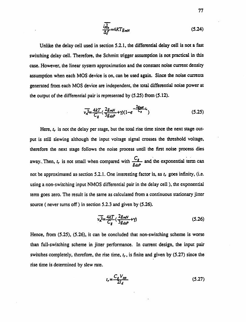
77
%**KT8mN (5.24)
Unlike the delay cell used in section 5.2.1, the differential delay cell is not a fast
switching delay cell. Therefore, the Schmitt trigger assumption is not practical in this
case. However, the linear system approximation and the constant noisecurrent density
assumption when each MOS device is on, can be used again. Since the noise currents
generated from each MOS device are independent, the total differential noise power at
the output of the differential pair is represented by (5.25) from (5.12).
v^^+TXW"^*) (5.25)Here, tr is not the delay per stage, but the total rise time since the next stage out
put is still slewing although the input voltage signal crosses the threshold voltage,
therefore the next stage follows the noise process until the first noise process dies
r
away..Then, tr is not small when compared with -—*— and the exponential term can
not be approximated as section 5.2.1. One interesting factor is, as tr goes infinity, (i.e.
using a non-switching input NMOS differential pair in the delay cell), the exponential
term goes zero. The result is the same as calculated from a continuous stationary jitter
source (never turns off) in section 5.2.3 and given by (5.26).
*=if(IS^ (5-26)Hence, from (5.25), (5.26), it can be concluded that non-switching scheme is worse
than full-switching scheme in jitter performance. In current design, the input pair
switches completely, therefore, the rise time, tr, is finite and given by (5.27) since the
rise time is determined by slew rate.
,r=£^0L (5.27)

78
Here, Id is half of the cell bias current flowing in the current source in the differential
cell and Vpp is the peak-to-peak voltage swing ofthe output V^. The slew rate also
determines the slope of the rise time. Hence,
&=2£ (5-28)Therefore, the jitter variance generated from one delay cell is represented by (5.29).
tfJ^fr^M^^) (5.29)If IgdsP
If there are N stages in the ring oscillator ( 2N switchings in one period ), the total
jitter variance in the ring oscillatoris,
where X= e ** . To see the effect of the size of the differential pair, each vari
ables in (5.31) are replaced by the following basic parameters.
Cg^Cgsn+^WnLnCox+Cs (5.31)
where Cs is the stray or parasitic capacitance.
g^HT-VnCoxiVgsn-VTn) (5-32)
w
/*-j- ^f-urt Cox (Vgsn-VTn)2 (5-34)
Then, the total jitter power is represented by (5.35).
7-? MkT{WnLnC0X+Cs)(\-\)*l#~ {Wn/Ln)^Col(Vgsn-VTnr
... 2(Wn/Ln)\ln(VeSn-VTn) (5.35)

79
(5.35) can be divided into three terms. The first one is -^ri-, the second is -n^, andWf "n
the last one is K^ based on the dependencies on Wn. As Wn increases, the jitter power
decreases because the first and the second terms decrease while the third term is con
stant Therefore, to control the jitter to an acceptable value, it is necessary to use large
device for the differential pairs in the delay cell. Also, from (5.30), to reducethe jitter,
large cell bias current is preferred. If (5.35) is further approximated to give some
insight, then,
^=iUCOT7(1+T-XW ^t, (5.36)
where ay is stage gain given by av=-722L- (5.36) can be further simplified intogdsP
(5.37). .
Aqfrt? r iNvkI (l+favXl-e"51^) (5.37)*~gn *dsatn J
L2where Xr is the NMOS device transit time given by i/1 . Hence, the normalized
Kn vdsatn
jitter variance is given by (5.38).
IT" vsr(^r)(1+^)(1"e ) (5,38)
From (5.38), the normalized phase jitter based on the device transit time, Xy, is pro
portional to \ t-£-, inversely proportional to Vdsatn and a weak function of the stage
gain, ay.
5.2.3 Non-Saturated Ring Oscillator
In this third ring oscillator type, the delay cell devices never rum off. Therefore, the

80
delay cell can be approximated as an linear amplifier. Here, again thedifferential ring
oscillator in figure 5.6 is used as an example. However, in this case, the input NMOS
pair devices are always on. Equations (5.23) and (5.24) are still valid since they are
derived when PMOS and NMOS devices are on. Again, if the equivalent noise circuit
can be represented as shownin figure 5.4, then the total differential noisepower at the
output of the differential pair is represented by (5.39).
Since the 3dB cutoff frequency of the differential pair is ^g »(5-39) becomeso
(5.40).
This result is exactly same as (5.26). Therefore, the jitter variance generated from one
delay cell is represented by (5.41).
5^Sl(yi.^s!!L) (5.41)
Again, if there are N stages in the ring oscillator, the total jitter variance in the ring
oscillator is,
ZtfJMjpL^Zjg.) (5.42)
Using the same basic parameters used in section 5.2.2, the total jitter can be approxi
mated by (5.43).
^xft ***[ )(l+|flv) (5.43)^gn "dsain **
Hence, from (5.43), as before the jitter is proportional to the device transit time, pro
portional to \ 7-2--, inversely proportional to Vdsatn* and linearly dependent on stage

81
gain. Here, the phase jitteris worse than that of the slow-slewing saturated ring oscil-
2Va
latorbyl/(l-e a7^).dy VAmi
5.2.4 Comparison of Ring Oscillator Jitter Performances
In this section, the jitter performance of the three different types of ring oscilla
tors is compared in table 5.1. In this table, key assumptions are summarized and the
jitter equations are described in terms of the intrinsic device transit time Xj. From this
table, it can be concluded that the fast-slewing saturated ring oscillator can achieve
the best jitter performance, the slow-slewing saturated ring oscillator shows the
second best, and the non-saturated ring oscillator shows the worst.* Therefore, a ring
oscillator composed of completely switching delay cells with fast slew rate is desir
able when low jitter performance is required.
* It is not immediately obvious that the fast-siewing saturated ring oscillator shows better jitterperformance than the slow-slewing saturated ring oscillator since the comparison was performedbetween single-ended and differential delay cells, respectively. However, if a differential delaycell (figure 5.6) with high slewing inputbuffer is used in the fast-slewing saturated ringoscillator( which perhaps could be implemented in BiCMOS process ), the comparison will be obvious.Here, from (5.25), the risetime, ir is replaced by nominal delay lime, t for the fast-slewing saturat-
ed type. Therefore, total jitter in the Nstage ring oscillator is given by (*.l) since x<K-^Jp«
5-"^»JB-> (M)Using the same parameters used in section5.2.2,equation (*.l) becomes(*.2).
Here, vw=2av is assumed. From (*.2), the jitter of the fast-slewing saturated type is 2 X smallerthan the minimum possible jitter of the slow-slewing saturated type. The reason is, in the fast-slewing saturated type, the noise process affects the delay only up to to the time point when theoutputof the previous delay cell crosses the threshold voltage. But, in the slow-slewingcase, thenoise process affects the delay for the full rise time andthis gives the penaltyof 2.

82
ring oscillator type
fast-slewing saturated
slow-slewing saturated
non-saturated
Table 5.1
key assumptions
non-stationary noise process
fast-slewing input buffer
full switching, single-ended
non-stationary noise process
no buffer
full switching, differential
stationary noise process
no buffer
no switching, differential
Ar^/x£
64NkT f AV xZC.VhatKVdla7
-*^(l+laV)(l^~~5^)
*NkJ il+lay)C8V£at T
5.3 PLL Phase Noise Accumulation
In this section, based on the jitter equations derived above, the PLL jitter at the
system level is analyzed. In the ring oscillator, if a clock pulse has a phase shift at a
certain time, the phase shift will remain forever because there is no correction
mechanism in the ring oscillator. For example, if a phase shift of a clock pulse at time
nT from a single jitter event which is caused by an accumulated jitter through the
inverters in the ring oscillator occurred, the phase shift will persist in the following
clock pulses as shown in figure 5.7(a).

83
ClockA/, Ar,
(a) Ring Oscillator Jitter for a Single Event
ClocKAr« Ar.
(b) Phase-Locked Loop Jitter for a Single Event
(c) Jitter vs Time for Multiple Events (PLL)
Figure 5.7 PLL Jitter Accumulation
However, if the ring oscillator is locked into the reference clock via a phase-
locked loop, the phase shift will be reduced because of the correction mechanism gen
erated by the phase-locked loop as follows. First, the phase detector detects the phase
shift, controls the charge-pumping circuit to generate charge to be stored in the loop
capacitor and to control the ring oscillator to adjust phase shift in the correct direction.
Since the amount of phase adjust is small, the phase shift is notcorrected in onecycle,
but it is reduced gradually in the following cycles as shown in figure 5.7(b). If we
measure the phase shifts for multiple jitter events and draw a diagram of phase shifts
vs time, we can get picture like figure 5.7(c). Note the different scale here. Therefore,
the result total phase jitter for those multiple events is shown in the dotted line in
figure 5.6(c).

84
To find the rms jitter, a PLL which uses a sequential phase detector and a
charge-pumping circuit can be represented by asimple discrete-time model as shown
figure 5.8 since the charge-pumping circuit can be represented by a switch connected
to current sources. Here, the phase jitter is a noise source added to the output clock
phase of the voltage controlled oscillator.
^x —* Kd » ZF(s)
m
\* Krn s
*%
Figure 5.8 PLL Linearized Model
Then, the transfer function of ©^(z) in terms of 0n(z), the phase jitter, is
represented by (5.44).
(5.44)
where Kd and Kf are the phase detector gain and VCO gain respectively, and Z/r'(z)
is the z-transform of the sampled version of Zp(s)/s. If the loop filter is assumed to
be a lead-lag filter composed of aresistor, R, in series with a capacitor, C. Then, the
above equation becomes (5.45).
(l-z-i)20n(z)0*«(z)=- T7K7T(\+KdKf)H?l^-KdKf-2)z-i+z-2
(5.45)
/ RT Afwhere Kd~ \ , and Kf=^L- Jp indicates charge pumping current In PLL's,

85
usually,
f^L«KdKf«\ (5.46)
Since dnX «KdKf and ^K/«l, we can ignore dni and put e=/Q£/.
Then, the transfer function is,
e<*('>~ i-(i-e)z-l (5'47)
Since the phase jitter coming from the ring oscillator is a sequence of step phase
jumps which have random magnitudes, a single step phase jump event at time n can
be represented by (5.35). Here, the magnitude of the step is Arn.
e"(2)=rS!% (5-48)Hence the output jitter in z-domain is,
27tA/n
e-(*)=r(i-(i4z-i) (5'49)
Therefore, in time domain, the output phase shift for a single event of the phase jitter
is represented by (5.50).
®on (n7)=^L(l-e)«u(nT) (5.50)
where u (nT) is the unit step function. For all events up to time nT , the sum of output
phase shifts is represented by (5.51)
e„(n7> t ^-(l-e)«-* (5.51)
To find the RMS jitter, the expectation of the square of the sum is calculated as fol
lows.
E[0,i {nT )}=E [(t£j2pL(i-ey>-* X£>^l(l-e)«-<)] (5.52)

86
Since Ar* and Ar/ are not correlated, the E[Ar*Ar/]=0 when k*L When £=/,
£[Ar*Ar*] can be replaced by Ar/?. Therefore, (5.52) becomes (5.53).
E[6& (nT )M^)2^Jjj(l-*)2rt (5-53)
Again, (5.53) can be simplified as (5.54)
Note that the expectation value of the phase jitter is independent of nT, the time
instant. Hence, the RMS phase jitter is,
^E[Q^nT)]^l^-=^ K*Kf **%* (5.55)where Afrm, is vA*$.
Comparing this value with the oscillator jitter, we can find the RMS time jitter in
aPLL is y *ff*» times larger than that of the ring oscillator. Here, the PLL accu
mulated the phase jitter. In the case of the analog PLL used in the hybrid clock
recovery circuit, the ratio is large. Therefore, the ring oscillator jitter should be very
small. Inchapter 5.5, an example case is given and the phase jitter is calculated.
5.4 DLL Phase Jitter
An alternative scheme to generate multi-phase clocks is to use a delay-locked
loop (DLL) [11]. Figure 5.9 shows the DLL schematic diagram.

Rtfercnca
Clock
Figure 5.9 DLL Schematic Diagram
87
Here, the reference clock coming from a crystal oscillator is fed to the input of
the delay line, and the rising edge of the output of the delay line is compared to that of
the reference clock. Since the rising edge of the reference clock reaches the output of
the delay line by passing through all delay cells, the total delay is one period of the
reference clock. If the total delay is smaller than the period of the reference clock, the
loop creates a correction voltage and causes the total delay to be the same as the
period of the reference clock. For example, if the rising edge of the output is lagging
behind of that of the reference clock, the phase detector generates positive correction
charge, increasing the output of the loop filter and reducing the total delay of the delay
line. Since the output of the loop filter just changes the phase of the output of the
delay line, the loop does not have any extra poles as a PLL does. Therefore, the stabil
ity problem is relaxed and a simple capacitor loop filter can be used without any sta
bility consideration.
In the delay-locked loop, the phase jitter is not accumulated because the jitter
created from one event of phase shift flushes away at the end of delay cell and never
accumulates. To see this, a simplified discrete time DLL model is used in figure 5.10.

88
'<>. Kd ZF(s)
O0«
Figure 5.10 DLL Linearized Model
Here, the DLL has avoltage-controlled or current-controlled delay generator andthe PLL has avoltage controlled oscillator. If the loop filter in the DLL is asinglecapacitor, the transfer function for output jitter vs delay generator in z-domain is
represented by (5.56).
&on (z ^—KTZTn 7(5.56)
where ^ is phase gain and given by -£p and Kp is phase gain and given by -35-. In
DLL, usually,
***,£-«l (5.57)
From (5.57), we can put e=^-. Then, the transfer function is represented by
(5.58).
(l+ej-z-1 v* l-(l-e)z"
The delay generator jitter is represented by (5.59) because the jitter is asingle phaseshift event and flushes away through the end of the delay chain.
(5.58)

89
0fl(2)=i^L (5.59)
Hence, the output jitter caused by a single phase shift event is,
eOT(z)=i^-(l-H1fe)z.1) (5.60)
In time domain, the output jitter is represented by (5.61).
eon(nT)=2Z^(S(nTye(\-eru(nT)) (5.61)
For all events up to time nT, the sum of jitter is,
0io<(*7>-y- ±*tk(l+z(l-e)»-k) (5.62)
Hence, the RMS jitter can be found as was (5.63). The result is,
V£[0r2/(wr)]=i^L (5.63)
Again, note that the RMS value is not function of nT.
In DLL case, as seen from (5.63), there is no jitter accumulation in a DLL.
Therefore, the jitter of the DLL is much smaller that that of the PLL which is nor
mally used in a clock recovery circuit.
5.5 Example: PLL Noise Analysis with Slow-Slewing Saturated Ring Oscillator
As an example, the PLL jitter using a slow-slewing saturated ring oscillator
using differential delay cell shown in figure 5.6 is calculated. Here, if N=32,
Cg=352fF, /rf=250|M, -^=2, Vpp=\.0Volts, and V^=0.3Vo/rj, thenods
'Attf=Q.94ps using (5.30). This is a reasonably good result when compared with the
measured value in chapter 7.

90
The PLL noise jitter is then calculated using (5.55). Since the jitter accumulation
/ / RTfactor is ^ ^K ' first Kd is calculated* Since K* is -^jrtKf=5MHz/voltt and/?=180a, KdKf=1.8X10-*. Here, /p is the value of the current generated from
charge-pumping circuit. Therefore, the accumulation factor is about 53. Hence, the
RMS jitter from the PLL is 50p*. The measured jitter including sampling jitter is
about 100/w, and this is approximately equal to the calculated value.
The next four graphs show the relations between PLL jitter and several important
parameters. Figure 5.11, 5.12, 5.13, and 5.14 show PLL jitter as a function of stage
gain, input gate width, channel length, and gate capacitance per unit area (Jim ),
respectively. Here again, the type of the ring oscillator is assumed to be a slow-
slewing saturated shown in figure 5.6 and equation (5.35) is used tocalculate the jitter.
The nominal parameters used in this equation are summarized in Table 5.2.
If the prototype is implemented in a scaled CMOS technology with constant vol
tage scaling (table 4.1), jitter performance of the prototype can be predicted from the
above four figures and equation (5.36). In constant voltage scaling, the gate width and
channel length are divided by aconstant factor k, the oxide thickness is divided by the
same factor, and substrate doping is multiplied by the factor of k\ while the voltage
source and Vj is maintained to a constant. Figure 5.12 shows the jitter performance
degradation with the scaled gate width. On the other hand, figure 5.13 and 5.14 show
the jitter performance enhancement with the scaled channel length and gate oxide,
respectively. Here, Cox=-^-. As a result, the time jitter decreases by the factor of
k3/2 (5.36). However, the relative time jitter to the intrinsic device transit time
increases by the factor of km from (5.38). Since the relative jitter performance deter
mines the maximum phase resolution of the hybrid analog/digital PLL, the constant
voltage scaling degrades the phase resolution and the maximum effective decoding
window defined in chapter 3.

Table 5.2
Parameter Value
Wn 160um
U 2um
wp 36(im
h 3um
Vgsn ~*Tn 0.3 Volts
Vgsp^Vjp 2.2 Volts
Cox 0.84 fF/um2
Cjo 0.20 fF/u.m2
Vpp 1 Volts
91

92
jiner secx 10"^
^,
plotO
/
/
1
•
stafl
68.00
66.00
64.00
62.00
60.00
S8.00
56.00
54.00
52.00
50.00
48.00
46.00
44.00
42.00
2.00 4.00 6.00 8.00 10*00
Figure 5.11 Phase Jitter vs Stage Gain

jitter sec x 10"^180.00
0.00 100.00 200.00 300.00 400.00
Figure 5.12 Phase Jitter vs Input Gate Width
93
500.00

94
jiner sec x10"12
400.00
380.00
360.00
340.00
320.00
300.00
280.00
260.00
240.00
220.00
200.00
180.00
160.00
140.00
120.00
100.00
80.00
60.00
40.00
20.00
0.00
plot2
/r
// 1
s^
^y
.. 1 length ia-xH 0*0.00 2.00 4.00 6.00 8.00 10.00
Figure 5.13 Phase Jitter vs Input Channel Length

jiner sec x10"^
220.00
210.00
200.00
190.00
180.00
170.00
160.00
150.00
140.00
130.00
120.00
110.00
100.00
90.00
80.00
70.00
60.00
50.00
40.00
30.00
20.00
10.00
0.00
plot3
111111I
1 .
\\\\\\\
\
CoaTj nmA2 x 10-151.00 2.00 3.00 4.00
Figure 5.14 Phase Jitter vs Gate Capacitance per Unit Area
95

96
5.6 PLL Phase Jitter System Simulation
To verify the PLL jitter accumulation phenomenon which was analyzed theoreti
cally in section 5.3, a simple behavioral simulator using the C programming language
was written. Figure 5.15 showsthe block diagram of the simulator.
Reference
Clock wPhase
Detector
*.Charge-Pumping
Circuit
*Lead-lag
Loop Filterj*
Local p-»y
Clock
r\ VCO
Vi
Jitter
Generator
Figure 5.15 Analog Phase-Locked Loop Jitter Model
• Here the VCO phase jitter is modeled by a Gaussian Markov Process and gen
erated from the gaussian random number generation module. Figure 5.16 shows the
jitter process.

97
a
e, 1
(N-1)T NT (N+1)T>t
Figure 5.16 Markov Process Model for Random Jitter in Ring Oscillator
The whole PLL loop has a phase detector and a lead-lag loop filter, as described
in chapter 4. The VCO is modeled by a linear FM modulator with phase jitter source
mentioned above. Figure 5.17 shows the phase jitter accumulation for the first 100
cycles and figure 5.18 shows the phase jitter accumulation for 50,000 cycles with
decimation ratio of 100. From these pictures, significant phase jitter accumulation is
evident.

98
jitter nsx 10"3
1-4-
I \ti-tr
'U
150.00
100.00
50.00
0.00
-50.00
•100.00
-150.00
•200.00
-250.00
-300.00
-350.00
-400.00
-450.00
i \l
/m4
Hi:ji
A
Vii—l.
t : f \M
tl\ p"
VI
0.00 20.00 40.00 60.00
in
jit_in
jitjout*
80.00 100.00
cycle
Figure 5.17 Phase Jitter Accumulation for 100Cycles

99
0.00 100.00 200.00 300.00 400.00 500.00
cycle
Figure 5.18 Phase Jitter Accumulation for 50,000 Cycles

100
Chapter 6
Optimal K Sequence for the DPLL
6.1 Introduction
Since the hybrid analog/digital clock recovery architecture allows the process ofacquisition and tracking to move from the analog domain to the digital domain, greatversatility is gained from the digital signal processing. One of the main goals of the
DPLL is to achieve fast acquisition while in addition still satisfying the constraint of
achieving large input jitter reduction. But two requirements are in conflict with each
other since fast acquisition requires very wide bandwidth in the DPLL loop, whilelarge noise reduction requires very narrow bandwidth. To meet both requirements, agear-shifting method has been used in conventional clock recovery circuits. However,
since the conventional clock recovery circuits rely on analog PLL's, and the loopcapacitors, or loop resistors of the analog PLL should vary in order to change the loopbandwidth, the selection of gear-shifting has been limited to very simple ones. On theother hand, the DPLL has no limitation in the selection of the gear-shifting parametersbecause there are no physical resistors and capacitors which determine the loopbandwidths and because a simple multiplying constant, Kcan be changed to controlthe loop bandwidth. Hence, the study of an optimal Ksequence which can meet the
the requirements of fast acquisition in preamble period and large jitter reduction indata decoding period is presented in this chapter.
6.2 Problem Definition
Figure 6.1 shows the DPLL block diagram. Here, each block can be implemented by a real digital multiplier, digital subtractor, accumulators and so forth. Here

101
the Kis the control parameter for the loop bandwidth. IfKis ~, the loop has infinite
bandwidth,and if K is 0, the loop has zero bandwidth.
©i
<fr
Figure 6.1 Linearized First Order Digital PLL Model
Here, each symbol is defined as follows.
®, : real input signal phase (fixed)
®N(n): jitter noise phase at time nT
©i(/i): input signal phase at time nT
®0 (n): DPLL output signal phase at time nT
K(n): K (control parameter) number at time nT
Therefore, the input signal phase is represented by (6.1)
®i(n) = ®s+QN(n) (6.1)
Since the jitter noise usually behaves as a wide-sense stationary white gaussian pro
cess, the jitter mean value and variance isrepresented by(6.2), (6.3) respectively.

102
E[eN(n)]=Q (6-2)
E[®fi(n )] =C# (6.3)
From the model shown in figure 6.1, the output phase from DPLL is given by (6.4).
®0 (n+1) =®0 (n )+K (n )(Bi (n )-©„ (n)) (6.4)
Rearranging it, then (6.5) is obtained.
®o(n+l) = (l-K(n))e0(n)+K (n)®i(n) (6.5)
Since (6.5) is a equation of for a nonlinear time-varying system, finding the
optimum K *s is a problem of optimization of a nonlinear time-varying system. In
general, it is very difficult to find a solution of the optimal parameters in a nonlinear
time varying system. However, in this case, an optimum set of K values exists and is
found as shown in the following sections.
Two different situations occur in the optimization process. First, for each instant
including preamble period, the difference between output phase and real input phase
should be minimized, i.e. the output phase should be the best estimation of the real
input phase. Since the input jitter is statistical process, the optimization is also based
on a statistical optimization criterion. Hence, the selection of K(n) at time nT should
be based on the minimum mean square criterion and given by (6.6).
MSEn=E[(®0(n)-®s)2] (6.6)
On the other hand, the optimization of K sequence for the whole period of preamble,
Pt should be a choice of a set of K values, K(Q)JC(\)JC(2) JC(P) which satisfy
the following minimum mean sum of squares criterion.
MSSEp =E((£(©* «)"©* )2] (6-?)
Here if the optimization is required for the whole period including the normal data
decoding, the criterion for theoptimal K sequence should be based on (6.8).

103
MSSE„=Enf^Bo (i )-©, )2] (6.8)
Two questions arise from these criteria. First, is the optimal.solution of K's for
the finite period of P same as that of ff's found from P-**> ? Le. Is the solution
independent ofP?The second question is, are the solutions found from (6.6) the same
as the AT values in the optimal set found from (6.7) or (6.8)? In this chapter, two
optimal solutions of K's are calculated based on (6.6), (6.7) and two questions are
answered by investigating the two results. As aresult, it is discovered that only one
optimal set of K's exist which satisfies the three criteria.
6.3 Optimization based on Minimum Mean Square Criterion
From (6.5), the difference between output phase at time nT and the real input
phase is expressed as (6.9).
.®o(n+\yes =(\-K(n))(®0(n)-®s)+K(n)eN(n) (6.9)
Let, prediction error,
®dM = ®0(n)-®s (6.10)
Then, (6.9) becomes (6.11).
®d(n+\)= (\-K(n))Qd(n)+K(n)eN(n) (6.11)
Since, initially S0(0) =0, the first output phase 0O (1) becomes (6.12).
e<,(l) =^(O)(0,+8/v(O)) (6.12)
Hence, the first phase difference is,
0<*(D =-(l-K(O))0,+K(0)®N(Q) (6.13)
Define,
c2(n) = E[®Kn)] (6.14)

104
Then minimization of (6.14) becomes the minimization of (6.6). But,
E[e2(n+l)] »E[((l-tf(n ))®d(n)+K(n)eN(n))2] (6.15)
Then, (6.15) becomes (6.16).
Elefti+l)J=E[(l-K (n ))2Ql(n )+K2(n )8j?(n )+2(l-AT(/i ))K (n )®d(n )®N (n)} (6.16)
Since 0</(n) =0o(n)-0J, and ®0(n) is a function of 9sK(Q),...JC(n-l), and
0^(0), 0N(n-l), £[0rf(n)0N(/t)] =O, where E[®N(k)®N(n)] =0 if k*n.
Therefore, (6.16) gives (6.17).
a2(n+l) =(\-K(n))2o2(n)+K2(n)ofi (6.17)
Also, from (6.13),
o2(l)=(\-K(Q))2®frK2(0)ofi (6.18)
From (6.17) and (6.18), it is seen that minimization problem of o2(n+l) for K(0) is
minimization problem ofa2(/i), and it is again the minimization problem ofa*(/i-l),
and finally the minimization problem ofa2(l). Hence, first minimization ofa2(l) is
necessary. Since o2(l) is a convex function of K(Q), the minimum value of it is
found at ^$ =0. Therefore,
|£jjj.=-2(1-* (O))0j^-2K (Q)c& =0 (6.19)
Then, the value K(0) which satisfies (6.19) is given by (6.20)
*<0)=w (6-20)
Also, the minimization of c2(2) gives (6.21).
™-a&r (6-21)In general, K(n) is represented by (6.22).

105
The minimum value of o2(n +1) using optimal K values is given by (6.23).
ofafr+l)- *ffi.-i ("3)(n+1)0,2+O/J
As n goes large number,
v- 1KOiF-^T <6-24>
and,
okOi+1)^ (6.25)
In the case that ©/»a#,
tf(n> =-4r <6*26)
and,
ami„(«+D =Ji- (6-27)
6.4 Optimization Based on Minimum Mean Sumof Squares Criterion
To find the optimum solution which satisfies the criterion (6.6), (6.28) should be
minimized.
MSSEN =£c2(/) (6.28)
To find theK (0) which minimizes equation (6.28), (6.28) is differentiated.
AS0*>-SW-^SjS(1-*(/-1))2S& (6-29)Since, uJL\ fto2(i) =0means ^0) =0, the optimal value which minimizes

106
(6.28) is the optimal value which minimizes (6.18) and the result is given by (6.20).
In general,
^k^^Mj^'-^^r1 (6-30)(6.30) also gives the same conclusions that optimal K values based on MMSSE cri
terion is same as those based on MMSE criterion. Hence, again
™--5SIW«*- (6-31)
°2^j^hr (6-32)Since the optimal K sequences that minimize the equation (6.28) are independent
of the finite period N, the Ksequences are again the optimal solutions which minimize
the equation (6.8).
To verify the optimal K sequences, a simple simulation program was written
using C programming language. Four sets of K sequences are tested for the real time
phase acquisition and for the signal-to-noise power ration when the signal is normal
ized to "1" and jitter noise isassumed to have agaussian distribution with the standard
deviation of 0.15. Figure 6.2, and 6.3 show the real time phase acquisition up to 100
bit cycles in two different noise environments. Here, in indicates the input jitter
noise. First, out indicates the phase acquisition when the optimal K sequences was
used. Second, out2 indicates the phase acquisition when 2n approximation for the
optimal K sequences is used. For example, 1/3 ,1/4 are approximated as 1/4. Third,
out3 indicates the four step K sequence, which are K = 1,1/2,1/2, 1/4,1/4,1/4,1/4,
1/32, .... Finally, out4 indicates the fixed K sequence, where K =1/32. The input
statistics are shown in table 6.1.

107
Table 6.1 Input Jitter Noise Statistics
gaul.dat
Statistics: x
Col N Mean SD Min 25% 50% 75% Max
1 100-0.000676 0.1534 -0.3059 -0.1115 -0.01842 0.1254 0.3728
gau2.dat
Statistics: x
Col N Mean SD Min 25% 50% 75% Max
1 100 0.01336 0.1656 -0.3378 -0.09133 0.006263 0.1222 0.5608
Figure 6.4 show the signal-to-noise power ratio. Here, the numbers alsorepresent
the K sequences indicated the above. Significant signal-to-noise power ratio improve
ments are obtained when gear-shifting methods are used.

108
0.00
0.00 20.00 40.00 60.00 80.00 100.00
cycle
Figure 6.2 Real-Time Phase Acquisition Using Optimal KSequences (I)

109
0.00 20.00 40.00 60.00 80.00
'—, cycle100.00
Figure 6.3 Real-Time Phase Acquisition Using Optimal KSequences (11)

no
S/NdB
36.00
34.00
32.00
30.00
28.00
26.00
24.00
22.00
20.00
18.00
16.00
14.00
12.00
10.00
8.00
6.00
4.00
2.00
0.00
ssar
—.-~~"~~~°"~'ssnr2
ssnr3;£«.—•••"^
ssnx4
^-- 1 .'-'ii
>?' s—*
g *f *
/
/
ft*It
/
//
/
/ \
/1
/
/*
4
/1
1i
f
t
; j
• f
/
/
1
1l
1t
111
/
/11 1
/ 11
1 ' cycle
0.00 20.00 40.00 60.00 80.00 100.00
Figure 6.4 Signal-to-Noise Power Ratio Using Optimal K Sequences

Ill
Chapter 7
Experimental Results
7.1 Introduction
Two chips were fabricated to measure the performance of the hybrid clock
recovery method. The first one contains an analog PLL including the 32 stage ring
oscillator and parallel phase sampler. The second is the complete hybrid clock
recovery circuits and contains a digital PLL including the previous analog PLL and
parallel phase sampler. The chip is composed of a total of 20,000 transistors. Figure
7.1 shows the chip photo of the first one. The technology used here is a 2|im single
poly, double metal, N-well CMOS process. These chips are fabricated through
MOSIS.
7.2 Analog PLL and Parallel Phase Sampler
The ring oscillator in the analog PLL was tested first. The center frequency of the
ring oscillator was about 30MHz and its control range is +/- 15%. Since the control
range is one of the imponant factors in designing the VCO in order to be insensitive to
the process parameter variations, a larger control range is preferred. In this design, the
resistance of the PMOS load was changed to vary the frequency of the ring oscillator.
However, if the cell bias current is controlled, the control range will be much larger
than that of this design. In simulation, more than 80% control range is expected.

112
»•• Kg-owr<c— gg»g»irT^uc:oP^g«MQfflam
^iiilto:*iyiliimsi:tl||:|**f^^^^?W*T?W-rtr»-«-Mi^'»-ir.'»-"-<iM-it-i.i « «-*
uinxuiAftaanjiflftftfifU'tiiftivw
OT^TOgggggggygOTgroiwi:
sHgasae
ctfo 143 fo fo fo f575 t^SR
^sT£g
oHo^
Figure 7.1 Chip Photo for the Analog PLL and Parallel Phase Sampler

113
The second measurement is the temperature coefficient (TQ of the ring oscilla
tor free running frequency. Since, the chip can be operated at different ambient tem
peratures depending on the environment, asmall TC is required so that PLL locking is
maintained over a wide range of temperature variation. In the hybrid clock recovery
circuit, since temperature stablized biasing circuits for the voltage and current sources
are embedded, the resulting TC is62ppm/deg C. This value isvery small and compar
able to the value announced in [TP LIU].
Power supply sensitivity of the ring oscillator free running frequency is also
imponant since power supply voltage can vary from place to place. In this case,
4.5%/volt power supply sensitivity was measured. This value is a little bigger than
expected: the reason is that one of the voltage-to-current conveners has asmall com
mon mode rejection ratio, and the control voltage changes according to the power sup
ply variations.
The second measurement was performed on the analog PLL. Figure 7.2 shows
the input clock waveform and the locked PLL output clock waveform. The waveform
degradation comes from wire inductance and power supply noise.
INPUT CLOCK
OUTPUT CLOCK
Figure 7.2 Input Clock and PLL Output Clock Waveforms

114
One of the key performance parameter is sampling jitter (this includes the PLL
phase jiner). Figure 7.3 shows the experimentally measured sampling jiner. Here the
analog PLL in the clock recovery circuit (DUT) is locked onto the reference clock (or
system clock) running at 30MHz. A precision delay is used to sweep the data transi
tion being sampled by the data latches in the clock recovery circuit Here, at each
sampling instant, the probability of "1" is measured for each delayed version of data
transitions and a graph of probability "1" (a distribution function) as a function of the
swept time delay is drawn. Here, the width of the transition from all "0" to all "1"
corresponds to the 6 sigma's under the assumption that the distribution is gaussian.
Therefore, 1sigma is 100 ps and this indicates that the RMS jitter is 100 ps.
Data In
Reference
Clock
Data In
Clock In
Data Separator
(DUT)-
—»Precision
Variable DelayI Data Out
1 ns
»i<Hi• i—»
t t tSampling Instance
1Probability of;'r
i r-4 f"
Data Out/
/
Delay i
t
ft ^ I-**
r
•♦0.25ns *0.5ns-0.5ns -0.25ns
».D-D
Figure 7.3 Sampling Jitter Measurement
Table 1 summarizes the experimental results from ring oscillator, analog PLL,
and parallel phase sampler.

Table 1
Measured Data, 5V, 25°C unless indicated
Ring Oscillator and Phase Sampler
Free Running Freq 30MHz
Std Deviation of Free-Run Freq, 0.84MHz(2.9%)
(2 runs, 20 devices)
TC of Free-Running Freq 62ppm/deg C
Supply Sens of Free-Running Freq 4.5%/volt
Power Dissipation 390mW#
Silicon Area, 2|im 10K square mils
Silicon Area, \\im** 4K square mils
115
♦Idiosyncraticof panicular level shift implementation- easily reduced to 300mW by
straightforward modification of one level shifter in datapath.
♦♦Taken from 1 Jimprototype layout, now in fab.
7.3 Hybrid Analog/Digital Clock Recovery

Figure 7.4 Chip Photo of Hybrid Clock Recovery Circuit

117
Figure 7.4 shows the chip photo of the complete clock recovery circuit This chip
includes an analog PLL, a parallel phase sampler and a digital PLL. Here, most
aspects of the digital PLL are programmable, so the chip size is much larger than
would be the case for PLLs dedicated to a specific purpose. The technology used here
is the sameprocess as for the previous chip.
One of the key performance issues of the clock recovery circuit is the jitter toler
ance and represented by the maximum effective decode window. To find the window
width, Bit error rate in the complete data detector was measured as a function of data
transition location in the window. Figure 7.5 shows the measured bit error rate vs the
pulse position in decode. Here the maximum effective decode window is the distance-8between the two crossing points where the bit error rate curve meets the 10 biterror
rate line. The measured maximum effective decode window was 31 ns, or 94% of the
full window width of 33ns. This is limited by a combination of the jitter mentioned
above and the sampling resolution (phase quantization noise).
Bit Error Rate •
Effective Decoding Window(94%)
/48
Figure 7.5 Decode Window Measurement
Pulse Position
In Decode Window

118
Because of the zero-phase start algorithm, phase acquisition is instantaneous,
limited only by the jitter on the first detected transition. Initial acquisition is followed
by aperiod of PLL operation with shon time constant to allow decay of phase error
due to jitter on the first transition. Then the loop time constant is shifted to a large
value for normal operation. Figure 7.6 displays the typical acquisition sequence show
ing error free data recovery with no preamble. Here the incoming data and the local
clock are at the same frequency but out of phase. The vertical lines are added to indi
cate the window boundaries. Each data transition contains all information concerning
the data and clock. From this picture, for each input pulse, the corresponding correcdy
positioned synchronized output pulse is generated from the data separator chip. The
first pulse is intentionally given 25 %jitter to inject error in the acquisition process.
The other parameters such as power dissipation, area etc. are summarized in
table 2.
1 —r
RESET^Viff
INPUT(RZ)
mm 4UJXLLLLWJJJ^IXMUJJJ^IXIJW •>TpJH^i*
OUTPUT DATA300ns Decode Latency
kYc\ Ftw ii^tTii iwi'^tii ictti in fp
± ±
200ns/cfrv
Figure 7.6 Typical Phase Acquisition Sequence

Table 2
Measured Data, 5V, 25°C unless indicated
Ring Oscillator and Phase Sampler
Free Running Freq 30MHz
Std Deviation of Free-Run Freq, 0.84MHz (2.9%)
(2 runs, 20 devices)
TC of Free-Running Freq 62ppm/deg C
Supply Sens of Free-Running Freq 4.5%/volt
Power Dissipation 390mW
Silicon Area, 2|i/n 10K square mils
Silicon Area, \\im 4K square mils
Complete Analog/Digital PLL
Silicon Area, 2\im 30K square mils
Power Dissipation 600mW
119

/
120
Chapter 8
Conclusions
8.1 Summary of Research Results
This research shows that the new architecture for clock recovery, called hybrid
analog/digital clock recovery is of potential interest in high speed data transmission
systems such as disk drive read-channels, local area networks, and optical transmis
sion. The research results are summarized as follows.
1. Hybrid analog/digital clock recovery technique is viable approach for clock
recovery in high speed data transmission systems.
2. In general, hybrid analog/digital clock recovery allows short preamble period (
1-2 bit cycles).
3. In general, an effective phase resolution of 1 ns in a 2 pm CMOS process is
achievable.
4. 'Jitter performance is improved using differential ring oscillator. Using large
• input devices in the delay cell, 100 ps RMS jitter is achieved.
5. A delay-locked loop further improves the jitter performance since it does not
have the problem of jitter accumulation.
6. In hybrid clock recovery circuits, maximum effective decoding window width is
virtually full since the decode window width depends only on samplingnoise.
7. The hybrid architecture allows the use of CMOS technology for high speed clock
recovery and incorporates the capability to implement sophisticated algorithms
in the digital domain.

121
References
[1] P. Gray, R. Meyer, "Analysis and Design of Analog Integrated Circuits", John
Wiley & Sons, 1984.
[2] D. Hodges, H. Jackson, "Analysis and Design of Digital Integrated Circuits",
McGraw-Hill Book Company, 1983.
[3] E. Lee, D. Messerschmitt, "Digital Communication", Kluwer Academic Publish
ers, 1988.
[4] J. Kellis, S. Mehrotra, "A 15 Mb/s Data Separator and Write Compensation Cir
cuit forWinchester Disk Drives", ISSCC, vol. 29, pp. 232-233, Feb. 1984.
[5] W. Llewellyn, M. Wong, G. Tietz, and P. Tucci, "A 33 Mb/s Data Synchronizing
Phase-Locked Loop Circuit", ISSCC, vol. 31, pp. 12-13, Feb. 1988.
[6] A. Bell, G Boriello "A Single Chip NMOS Ethernet Controller", ISSCC, vol. 26,
pp. 70-71, Feb. 1983.
[7] H. Haung, D. Banatao, G. Periegos, T. Wu, T. Chiu, "A CMOS Ethernet Serial
Interface Chip", ISSCC, vol. 27, pp. 184-185, Feb. 1984.
[8] K. Ware, H. Lee, C. Sodini, "A 200 MHz CMOS PLL with Dual Phase Detec
tors", ISSCC, vol. 32, pp. 192-193, Feb. 1989.
[9] US Patent 4,584,695, National Semiconductor, 1980.
[10] US Patent 4,189,622, NCR Corporation, 1977.
[11] J. Sonntag, R. Leonowich, "A Monolithic CMOS 10 MHz DPLL for Burst-Mode
Data Retiming", ISSCC, vol. 33, pp. 194-195, Feb. 1990.
[12] B. Kim, D. Helman, P. Gray, "A 30 MHz High-Speed Analog/Digital PLL in 2
urn CMOS", ISSCC, vol. 33, pp. 104-105, Feb. 1990.
[13] A. Jordan, N. Jordan, "Theory of Noise in Metal Oxide Semiconductor Devices",
IEEE Electron Devices, pp. 148-156, March 1965.

122
[14] F. Gardner, "Charge-Pump Phase-Locked Loops", IEEE Communications, vol.
com-28, no. 11. pp 1849-1858, Nov. 1980.
[15] F. Gardner, "Phaselock Techniques", Wiley-Interscience Publication, 1979.
[17] T. Liu, R. Meyer, "A 250 MHz Monolithic Voltage-Controlled Oscillator",
ISSCC, vol. 31, pp. 22-23, Feb. 1988.
[18] C. Tzeng, "Timing Recovery in Digital Subscriber Loops", UCB/ERL M85/29,
April, 1985.
[19] D. Messerschmitt, "Frequency Detectors for PLL Acquisition in Timing and Car
rier Recovery", IEEE Communications, vol. com-27, no. 9, Sep. 1979.
[20] C. Laber, C. Rahim, S. Dreyer, G. Uehara, P. Kwok, P. Gray, "Design Con
siderations for aHigh-Performance 3-jxm CMOS Analog Standard-Cell Library",
IEEE JSSC, vol. sc-22, no. 2, April, 1987.
[21] R. Leonowich, J. Steininger, "A 45-MHz CMOS Phase/Frequency-Locked Loop
Timing Recovery Circuit", ISSCC, vol. 31, Feb; 1988.
[22] K. Mueller, M. Muller, "Timing Recovery in Digital Synchronous Data
Receivers", IEEE Communications, vol. com-24, no. 5, May 1976.
[23] D. Jeong, G. Borriello, D. Hodges, R. Katz, "Design of PLL-Based Clock Gen
eration Circuits", IEEE JSSC, vol. sc-22, no. 2, April 1987.
[24] L. Bellato, G. Cariolaro, "Time Jitter in Line Regenerators with Pattern Depen
dent Pulse Waveforms", Alta Frequenza, vol. XLI-N.l 1,Nov. 1972.