![PDF [727 KB]](https://static.fdocuments.us/doc/165x107/586f55111a28ab3f228bbd63/pdf-727-kb.jpg)
Performance Testing of the iX Cameras i-SPEED 727 High ...
28
SANDIA REPORT SAND2021-3964 Printed April 2021 Performance testing of the iX Cameras iSpeed 727 high-speed camera Julien Manin Prepared by Sandia National Laboratories Albuquerque, New Mexico 87185 and Livermore, California 94550
Transcript of Performance Testing of the iX Cameras i-SPEED 727 High ...

SANDIA REPORT SAND2021-3964 Printed April 2021
Performance testing of the iX Cameras iSpeed 727 high-speed camera Julien Manin
Prepared by Sandia National Laboratories Albuquerque, New Mexico 87185 and Livermore, California 94550

2
Issued by Sandia National Laboratories, operated for the United States Department of Energy by National Technology & Engineering Solutions of Sandia, LLC. NOTICE: This report was prepared as an account of work sponsored by an agency of the United States Government. Neither the United States Government, nor any agency thereof, nor any of their employees, nor any of their contractors, subcontractors, or their employees, make any warranty, express or implied, or assume any legal liability or responsibility for the accuracy, completeness, or usefulness of any information, apparatus, product, or process disclosed, or represent that its use would not infringe privately owned rights. Reference herein to any specific commercial product, process, or service by trade name, trademark, manufacturer, or otherwise, does not necessarily constitute or imply its endorsement, recommendation, or favoring by the United States Government, any agency thereof, or any of their contractors or subcontractors. The views and opinions expressed herein do not necessarily state or reflect those of the United States Government, any agency thereof, or any of their contractors. Printed in the United States of America. This report has been reproduced directly from the best available copy. Available to DOE and DOE contractors from U.S. Department of Energy Office of Scientific and Technical Information P.O. Box 62 Oak Ridge, TN 37831 Telephone: (865) 576-8401 Facsimile: (865) 576-5728 E-Mail: [email protected] Online ordering: http://www.osti.gov/scitech Available to the public from U.S. Department of Commerce National Technical Information Service 5301 Shawnee Rd Alexandria, VA 22312 Telephone: (800) 553-6847 Facsimile: (703) 605-6900 E-Mail: [email protected] Online order: https://classic.ntis.gov/help/order-methods/

3
ABSTRACT This work evaluated the iX Cameras iSpeed 727, a commercial CMOS-based continuous-recording high-speed camera. Various parameters of importance in the scheme of accurate time-resolved measurements and photonic quantification have been measured under controlled conditions on the bench, using state-of-the-art instrumentation. We will detail the procedures and results of the tests laid out to measure sensor sensitivity, linearity, signal-to-noise ratio and image lag. We also looked into the electronic shutter performance and accuracy, as exposure time is of particular interest to high-speed imaging. The results of the tests show that this camera matches or exceeds the performance of competing units in most aspects, but that, as is the case for other high-speed camera systems, corrections are necessary to make full use of the image data from a quantitative perspective.

4
ACKNOWLEDGEMENTS The author would like to acknowledge Todd Rumbaugh of Hadland Imaging for the helpful discussions and for allowing us to borrow the camera for testing. This study was performed at the Combustion Research Facility, Sandia National Laboratories is a multi-mission laboratory managed and operated by National Technology and Engineering Solutions of Sandia, LLC., a wholly owned subsidiary of Honeywell International, Inc., for the U.S. Department of Energy’s National Nuclear Security Administration under contract DE-NA0003525.

5
CONTENTS 1. Introduction and background .................................................................................................................... 8 2. Camera specifications .................................................................................................................................. 9 3. Tests and results ........................................................................................................................................ 10
3.1. Pixel readout rate ............................................................................................................................ 10 3.2. Intensity response and sensitivity ................................................................................................. 11 3.3. Sensor response uniformity ........................................................................................................... 13 3.4. Image signal-to-noise ratio ............................................................................................................ 14 3.5. Exposure accuracy and shuttering variability ............................................................................. 16 3.6. Image lag .......................................................................................................................................... 19
4. Summary and conclusions ....................................................................................................................... 23
LIST OF FIGURES Figure 3-1. Pixel throughput as a function of framerate for the camera under study, as well as
other relevant high-performance camera units. .................................................................................... 10 Figure 3-2. Digital intensity level as a function of normalized illumination intensity under the two
analog gain settings. The dashed black line represents the end-point fit. The light sensitivity of the sensor for both gain settings are given in the lower right corner. ......................................... 12
Figure 3-3. Spatial response of the camera when comparing (I75/I25) two uniform illumination levels with a. factor three average difference. ....................................................................................... 13
Figure 3-4. Example of an image featuring a smooth gradient covering the full dynamic range of the camera and enabling full-scale measurement of the SNR. ........................................................... 14
Figure 3-5. Signal-to-noise ratio as a function of digital intensity under two gain settings. Each dot represents the SNR for a given pixel, while the dashed lines are the mean profiles. .............. 15
Figure 3-6. Signal-to-noise ratio as a function of digital intensity for data saved in both 8 and 16 bit depths. Each dot represents the SNR for a given pixel, while the dashed lines are the mean profiles. ............................................................................................................................................. 16
Figure 3-7. Exposure gate profile and associated SNR drop for a 2.5-µs exposure time setting. ....... 17 Figure 3-8. Top: Normalized spatial intensity measured during the transient opening period of
the exposure gate. Bottom: Histogram of intensity distribution for the map displayed above. ... 18 Figure 3-9. Camera behavior related to image lag. The top-left image is the background map, the
top-right shows the illuminated image, while the bottom left and right maps show lag on the two images following the illuminated sample (left: n+1, right: n+2). ............................................... 20
Figure 3-10. Magnitude of image lag for the subsequent two images as function of intensity difference between the illuminated frame and the background intensity distribution. .................. 21
LIST OF TABLES Table 2-1. Characteristics and specifications for the iX Cameras iSpeed 727 provided by the
manufacturer. ............................................................................................................................................... 9

6
This page left blank

7
ACRONYMS AND DEFINITIONS
Abbreviation Definition ADC Analog-to-digital converter
CMOS Complementary metal-oxide semiconductor
EMVA Europe Machine Vision Association
ISO International Standard Organization
LED Light-emitting diode
SNR Signal-to-noise ratio
UV Ultraviolet

8
1. INTRODUCTION AND BACKGROUND While progress in digital imaging in general is likely the result of commercial and industrial applications, scientific applications have been pushing the operating envelope of high-speed imaging over the past decades. In addition to their extensive use in movies and sports broadcasting, high-speed cameras are employed in a multitude of applications, including ballistic, explosions, fluid-dynamic, combustion, or vehicle crash-testing for advanced research and development, as listed by Fuller [1].
Nearly three decades ago, Etoh and his coworkers [2] introduced a high-speed CMOS sensor design capable of continuously recording several thousand frames per second. While not particularly groundbreaking with respect to imaging application at this time, where film technology provided higher rates and superior image quality, the digital aspect of this new device was very attractive. Advances in semiconductor technology have enabled high-speed camera systems to record rates of several million frames per second.
When used for scientific applications, certain aspects of high-speed cameras are subject to specific requirements. Image quality is most likely of interest to all users, but the criteria to evaluate image quality may vary widely depending on the need, from a simple qualitative visual assessment to more science-based metrics. As an example of the latter, Manin and coworkers [3] proposed a set of measurement procedures to evaluate high-speed digital cameras. The testing protocols aimed at assessing two of the latest and highest performance commercially-available high-speed cameras, in the scheme of scientific applications. It should be noted though that several tests were equivalent to common camera testing practices, and that other tests, while targeting high-speed cameras for scientific application, could very well be applied to any other digital camera systems. The two cameras tested demonstrated well-matched performance for typical aspects of digital camera systems, for which testing protocols are in place (linearity, signal-to-noise ratio, sensitivity) [4, 5]. However, there was more disparity in their performance regarding aspects more specific to high-speed cameras, such as exposure time (shutter) accuracy and precision, or image lag [Fossum2003].
Applying or extending the testing procedures proposed by Manin et al. [3], the current work aims at evaluating a newer generation high-speed camera. Equipped with a high-resolution sensor, the iX Cameras iSpeed 727 presents superior performance figures compared to previously available systems. The results of the tests are compared to currently available high-speed cameras aimed at a similar market, i.e., with similar specifications and anticipated performance. The comparisons gather both specified parameters, as well as test data from previous evaluation campaigns. The results support that, while not perfect, the iX iSpeed 727 offers state-of-the-art performance, matching or surpassing other competing camera systems in most aspects evaluated during these tests.
There are two main sections in this document between the present introduction and the summary and conclusions. The first one describes the camera specifications, relating the information to other similarly-specified high-speed cameras. The second and largest section presents the results of the tests, as well as the necessary information about the test procedures. As commented above, the results of the tests are put in perspective compared to other high-speed cameras, to provide a frame of reference and confirm the high level of performance of the subject of this study.

9
2. CAMERA SPECIFICATIONS The most relevant characteristics and specified performances of the camera are summarized in Table 2-1. Note that certain parameters require export-controlled options to achieve the level of performance given in the table below, and that the spectral response range is defined as the 10-% point relative to the full-scale spectral response curve.
Table 2-1. Characteristics and specifications for the iX Cameras iSpeed 727 provided by the manufacturer.
Parameter Value Sensor resolution 2072 x 1536 pix. (3.2 Mpix)
Sensor technology Custom CMOS
Sensor type Global shutter (monochrome)
Pixel size 13.5 µm
Bit depth 12-bit
Max. pixel readout 27.1 Gpix/s
Max. framerate 2,450 kfps
Min. exposure time 168 ns
Max. ISO sensitivity (no gain) 16,000
Spectral response 330 – 970 nm
High-speed cameras present a variety of aspects depending on the application they aim at serving. Considering the pool of commercially-available devices, the best match to the specifications of the iX iSpeed 727 would be the Phantom v2640. It also is equipped with a custom CMOS a high-resolution (4 MPix) sensor, with global shutter. It features square pixels of 13.5 µm in size and similar pixel throughput (26 Gpix/s). With the same pixel size, the ISO 12232 [4] sensitivity rating of 16,000 for the Phantom v2640 is directly comparable and matches that of the iX iSpeed 727. It can also be noted that the sensors’ dynamic ranges are specified as 64 dB for the Phantom v2640 and 65 dB for the iX iSpeed 727.

10
3. TESTS AND RESULTS This section presents the results of the tests performed to evaluate the cameras, but also provides brief descriptions about the respective test procedures. These procedures followed the guidance provided by Manin et al. [3] to evaluate high-speed camera systems. It should be noted that the results of certain tests depend upon the methodologies employed during testing. In an attempt to provide a frame of reference to the results of the tests, the data were compared to similar high-speed cameras that have been previously tested.
3.1. Pixel readout rate A key aspect of high-speed cameras is how fast they can record. For continuously recording cameras such as the unit investigated in this work, the pixel readout rate or pixel throughput is the main measure used to compare camera performance between different models. The pixel throughput (Rpix) takes into account both frame rate, as well as frame size, i.e., the number of pixels in the image. It can be calculated as follows:
𝑅!"# = 𝑅𝑒𝑠"$% ∙ 𝐹&'(, (1)
This metric follows the guidelines introduced by Manin et al. [3] to evaluate a camera’s effective readout rate. Resimg is the image size, namely the number of pixels being readout, easily obtained by multiplying the height and width of the digital image (in this 3.18x106 pixels at full frame). The acquisition rate Facq is the number of images acquired per second, or the operating frequency.
The pixel readout rate can be computed directly from the specification sheet associated with the camera and does not require any specific testing procedure. The results reported in Figure 1 applied Equation 1 to the framerate and associated image resolution over a range of acquisition rates for various cameras, all representing the state-of-the-art for continuous recording camera systems. Note that the data reported in this figure come from both the specification document, as well as our own testing.
Figure 3-1. Pixel throughput as a function of framerate for the camera under study, as well as
other relevant high-performance camera units.

11
The results of Fig. 3-1 indicate that in spite of these high-speed camera units competing for a similar market and presenting similar total throughput at lower frame-rates, there is a large spread at higher acquisition rates. All cameras in this plot present total throughput upwards of 20 Gpix/s, with three units above 25 Gpix/s. The Phantom v2640 was presented as the most direct competitor to the iX iSpeed 727 based on their specifications, but the iX iSpeed 727 pixel throughput is more than three times that of the Phantom v2640 at acquisition rates above 100 kHz. It should be noted that the readout rates reported in Figure 3-1 for the Phantom v2640 correspond to the high-speed binning mode, the fastest operating setting offered by this camera. Overall, the iX iSpeed 727 matches or exceeds the pixel throughput of all other cameras in this comparison plot, with the advantage growing as acquisition rates increase.
3.2. Intensity response and sensitivity The response of the camera to various levels of illumination intensity has been tested using a calibrated 8-in diameter integrating sphere equipped with a tungsten bulb, following the procedures described in Manin et al. [2018b]. The output radiance has been varied from immeasurable light level up to sensor saturation with the integrating sphere placed right against the camera’s F-mount, i.e., the output of the integrating sphere is located at the flange distance. To avoid potential bias produced by non-linearity in the camera’s response with intensity from a spatial perspective, the digital levels were averaged over a small region near the center of the sensor. For clarity, the digital camera level is presented as a function of the normalized radiance, with the maximum (value of 1) corresponding to sensor saturation.
The results of the linearity tests are shown in Figure 3-2, for the two analog gain settings available. Because of the random noise of all pixels of the sensor, the data were extrapolated to avoid pixels from reaching the bottom and top of the range but provide measurements over the entire digital scale offered by the camera, from 0 to 4095 Cts. The black dashed line represents a straight line joining both extremes (0 and 4095 Cts). This way of highlighting linearity deviation is called the end-point method and is commonly used to visually assess camera intensity response. Linear regressions were computed to provide least square estimators to the camera responses with a zero digital level intercept.
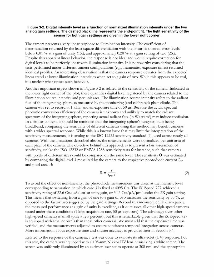
12
Figure 3-2. Digital intensity level as a function of normalized illumination intensity under the two analog gain settings. The dashed black line represents the end-point fit. The light sensitivity of the
sensor for both gain settings are given in the lower right corner.
The camera presents a very linear response to illumination intensity. The coefficient of determination returned by the least square differentiation with the linear fit showed error levels below 0.01 % at a gain of unity (1X), and approximately 0.20 % at a gain setting of two (2X). Despite this apparent linear behavior, the response is not ideal and would require correction for digital levels to be perfectly linear with illumination intensity. It is noteworthy considering that the tests performed under different camera configurations (e.g., framerates, exposure times) returned identical profiles. An interesting observation is that the camera response deviates from the expected linear trend at lower illumination intensities when set to a gain of two. While this appears to be real, it is unclear what causes such behavior.
Another important aspect shown in Figure 3-2 is related to the sensitivity of the camera. Indicated in the lower right corner of the plot, these quantities digital level registered by the camera related to the illumination source intensity and per unit area. The illumination source intensity refers to the radiant flux of the integrating sphere as measured by the monitoring (and calibrated) photodiode. The camera was set to record at 1 kHz, and an exposure time of 50 µs. Because the actual spectral photonic conversion efficiency of the camera is unknown and unlikely to match the radiant spectrum of the integrating sphere, reporting actual radiant flux (in W/sr/m2) may induce confusion. In a similar context, it should be reminded that the integrating sphere’s tungsten bulb being broadband, comparing the sensitivity of different cameras using this method may benefit cameras with a wider spectral response. While this is a known issue that may limit the interpretation of the sensitivity measurements, it is analog to the ISO 12232 sensitivity standard [4], used across nearly all cameras. With the limitations described above, the measurements were normalized per unit area of each pixel of the camera. The objective behind this approach is to present a fair assessment of sensitivity, unlike the ISO 12232 or EMVA 1288 sensitivity tests for instance, such that cameras with pixels of different sizes could be compared on the same level. The sensitivity Q was estimated by comparing the digital level S measured by the camera to the respective photodiode current IPD and pixel area A:
Θ = !"!"∙$
. (2)
To avoid the effect of non-linearity, the photodiode measurement was taken at the intensity level corresponding to saturation, in which case S is fixed at 4095 Cts. The iX iSpeed 727 achieved a sensitivity rating of 22.6 Cts/µA/µm2 at unity gain, or 34.6 Cts/µA/µm2 under the 2X gain setting. This means that switching from a gain of one to a gain of two increases the sensitivity by 53 %, as opposed to the factor two suggested by the gain settings. Beyond this inconsequential discrepancy, the measured performance at a gain of unity is excellent, as it outclasses all other high-speed cameras tested under these conditions (1 kfps acquisition rate, 50 µs exposure). The advantage over other high-speed cameras is small (only a few percent), but this is remarkable given that the iX iSpeed 727 is equipped with smaller pixels than these other cameras. We must add that the exposure time was verified, and the measurements adjusted to ensure consistent temporal integration across cameras. More information about exposure time and shutter accuracy is provided later in Section 3.4.
Related to the response of the camera, a test was done to evaluate its ultraviolet (UV) response. For this test, the camera was equipped with a 105-mm Nikkor UV lens, visualizing a white screen. The screen was uniformly illuminated by an excimer laser set to operate at 308 nm, and the appropriate

13
set of lenses. Of particular interest to combustion science, the chosen wavelength of 308 nm is below the 10-% spectral range response provided in Table 2-1, but the camera is still expected to be sensitive at this wavelength (or anything above 300 nm) based on the spectral response curve. A combination of optical filters was attached to the front of the camera lens in order to spectrally filter all wavelengths (over the expected range of the camera) but that of the excimer laser source. The camera was synchronized with the laser, which operated at 10 Hz. It is irrelevant because of the short laser pulse, but the exposure time of the camera was set to 2.5 µs. Ensuring proper time alignment by removing the spectral filter package, no signal was registered by the camera with the appropriate 308-nm filter installed. While the laser energy per pulse was not measured, the scattered intensity off of the screen should have been bright enough for the camera to register 308-nm light had it been sensitive to this particular wavelength. The results of this specific test give us the confidence that the camera unit we tested did not respond down to such short UV wavelengths.
3.3. Sensor response uniformity The same experimental setup with the integrating sphere output located at the camera’s Nikon F-mount flange was used to evaluate the uniformity of the camera’s response over the full sensor. In an attempt to minimize bias in spatially-dependent illumination intensity, the responsivity was computed by comparing the intensity recorded at two illumination levels, at about 25 and 75 % of full the digital scale (targeting a factor three difference in average measured intensity). The average maps were also background corrected, with the integrating sphere light source turned off. While not shown, the background map is essentially 0 Cts all across, with only a few pixels being non-zero. The spatial intensity response of the camera (I75/I25) is shown in Figure 3-3.
Figure 3-3. Spatial response of the camera when comparing (I75/I25) two uniform illumination levels
with a. factor three average difference.
Several comments can be made about the two-dimensional response of the camera. First, the bulk of the I75/I25 map appears to be close to the expected value of three. However, the edges present higher values, with as much as 10 - 15 % difference from the mean. The most surprising aspect of this map is the asymmetrical behavior of the intensity response, with noticeably higher values on the right side of the frame. Several factors can explain the non-uniform response of a sensor to photonic intensity, but such a result would indicate an erroneous calibration, as opposed to a known physical aspect. At this stage, it seems more likely that the results of this test were affected by illumination non-uniformities, coming from the interaction between the integrating sphere and the camera, inducing spatial differences in intensity as radiant flux was increased. While other tests revealed a suspicious performance regarding the camera’s response to intensity across the sensor, the results of Figure 3-3

14
and the surrounding discussion require further examination and testing to be validated and for conclusions about this aspect to be drawn.
3.4. Image signal-to-noise ratio The signal-to-noise ratio (SNR) of an imaging device is a paramount piece of information. It becomes especially important in digital systems when compared to the camera sensitivity to illumination intensity. In this work, the SNR was measured as a function of the digital level measured and reported by the camera (S, with intensity in Cts) using the following expression:
𝑆𝑁𝑅(𝑑𝐵) = 20 ∙ 𝑙𝑜𝑔 2)!*!3. (3)
In Equation 3, µS and sS are the mean and standard deviation of the signal S, respectively.
Several methods have been developed to estimate the SNR over the dynamic range of the camera. An efficient way to probe the entire dynamic range is to illuminate the sensor with a smooth intensity gradient covering the full intensity scale of the camera (from completely dark to saturation, or 0 to 4095 Cts) [3]. An example of such an image is given in Figure 3-4. A pulsed LED system was used to produce a short light pulse timed to coincide with the middle of the exposure. The LED output radiance was “collimated” by a large Fresnel lens to illuminate a large engineered diffuser. The camera was equipped with a 50-mm f/1.4 lens focused at infinity, while a straight edge of an opaque object was located at approximately 50 mm from the camera lens, such that the edge would be blurry, offering the smooth gradient desired for these tests.
Figure 3-4. Example of an image featuring a smooth gradient covering the full dynamic range of
the camera and enabling full-scale measurement of the SNR.
The SNR was then computed applying Equation 3 for all pixels of the sensor, except when the digital level measured by a given pixel approaches the bottom and top ends of the dynamic range (0 and 4095 Cts). The advantage of this method compared to changing the illumination intensity uniformly across the sensor is that the SNR can be obtained over the entire dynamic range with a single set of images. The results were confirmed at several intensities with the sensor uniformly illuminated to ensure that the SNR behavior is consistent across the whole sensor.
The results of the tests at the two gain settings are provided in Figure 3-5. Each dot represents the SNR performance for a given pixel, while the dashed lines are the mean of the respective distributions.

15
Figure 3-5. Signal-to-noise ratio as a function of digital intensity under two gain settings. Each dot
represents the SNR for a given pixel, while the dashed lines are the mean profiles.
The results indicate that the camera reaches a mean SNR level near 40 dB at full scale. This level is considered “excellent” by the ISO 12232 standard previously mentioned. Surprisingly, the SNR drops by about 2 dB when the camera operates at a gain level of 2, compared to unity gain. Comparing such remark with the sensitivity results of Figure 3-2 indicates that increasing the sensor analog gain offers no benefit in terms of quantification performance. In fact, these results suggest that the analog gain behaves like a digital gain, under which circumstances the reported digital levels are increased, but the SNR remains constant. While such performance is very good, other high-speed cameras have demonstrated superior performance in that area, with the Phantom v2512 reaching a peak SNR slightly above 45 dB at full scale [3]. But it is fair to note that this camera features much larger pixels than the iX iSpeed 727, and that larger pixels are expected to present superior SNR, as a result of the increased well depth and sensitivity (at least from a fundamental photonic standpoint).
In addition to the two gain settings, the camera offers two operating modes, one prioritizing image quality, while the other optimizes speed, i.e., acquisition rate. The speed-optimized mode is easy to understand; it applies the appropriate settings for the camera to operate at the fastest frame rate possible under all resolutions, enabling the device to achieve the high pixel throughput highlighted in Figure 3-1. According to the manufacturer, the camera clock speed driving the readout rate is slowed down to allow for longer settling times. One critical aspect of high-speed sensors featuring global shuttering is related to the reset noise. A major component of the random noise related to the pixel reset comes from the interaction between the capacitance of the photodiode and the resistance of the MOSFET channel. This noise results in what is generally referred to as kTC noise, which is temperature-dependent, and essentially induces variance to the reset level of each pixel between images. Lower readout clock speed and longer settling times do not directly impact reset (kTC) noise but are expected to enable better control on the reset level for each pixel, thereby lowering their variance (noise).

16
With that said, we performed the SNR test under these two modes, but the results were virtually identical, with an unexpected advantage to the Speed mode of up to 0.5 dB, achieved at full scale, over a range of acquisition settings (from 1 to 100 kHz).
Overall, these results demonstrate that the camera performs well, or as expected in comparison to other high-speed cameras of the same caliber. However, the SNR performance also means that the sensor presents an effective digital resolution on the order of 7 to 8 bits, while it is equipped with 12-bit analog-to-digital converters (ADCs). Figure 3-6 shows the SNR performance for images saved in 8-bit resolution and for the same images saved in 16-bit. We must remind the reader that the 16-bit images only contain 12-bit data; the 16-bit resolution comes from the format used to export the image data (16-bit TIFF).
Figure 3-6. Signal-to-noise ratio as a function of digital intensity for data saved in both 8 and 16 bit
depths. Each dot represents the SNR for a given pixel, while the dashed lines are the mean profiles.
The differences are nearly non-existent between the two datasets. A close look indicates that the images saved as 16-bit data offer a slight SNR advantage at lower intensity levels, with up to about 0.5 dB improvement in the lower 10 to 20 % of the dynamic range. While this does not mean that the camera could operate with 8-bit digitizers, though this is something worth exploring, but that saving the data in 8-bit would certainly be a good way to save storage space with only a minor compromise with respect to image quality. Whether this compromise is important or not depends on the application, the need for quantification, as well as the intensity range as registered by the camera.
3.5. Exposure accuracy and shuttering variability The precision and accuracy of the exposure time are important parameters regarding high-speed imaging. In this context, precision refers to the repeatability of the exposure gate temporal location (with respect to camera frame synchronization signals), assessing both opening and closing transients, as well as duration. Accuracy aims at quantifying the actual exposure duration compared to the camera setting (or camera-defined exposure). The profile of the exposure gate, measured in

17
terms of intensity as a function of time, has been measured using a high-speed LED illumination source set to produce sub-20-ns pulses, similar to the tests described in Ref. [3]. The results of these tests are plotted in Figure 3-7 for a 2.5-µs exposure time (software setting). The normalized mean intensity was computed over a small region (300 x 400 pix2) with a 50-ns time resolution. As described earlier, the results were computed and averaged over 100 images, as for most experiments reported in this document.
The increased variability observed during the transient opening and closing times was evaluated by applying Equation 3 to the mean signal level and associated standard deviation during the transient periods to assess the reduction in SNR.
Figure 3-7. Exposure gate profile and associated SNR drop for a 2.5-µs exposure time setting.
The exposure gate profile shown in Figure 3-7 highlights the good performance of the sensor when it comes to shuttering. Both the rise and fall times (10 – 90 %) are shorter than 100 ns, with 85 and 90 ns for the rise and fall times, respectively. The exposure gate duration taken at 50 % was estimated to be 2410 ns, but the camera-indicated duration (2497 ns) would be matched if taken at approximately 10 % of the digital intensity range for this test. Tests exploring other exposure times and frame rates demonstrated that the gate durations were in line with the camera-indicated duration (which can differ from the set value). This is a solid performance for the iX iSpeed 727, which easily edges out previously tested high-speed cameras in terms of rise and fall times.
The SNR drop profile of Figure 3-7 was generated by measuring the image SNR at each discrete time and comparing it to the mean SNR extracted when the gate is fully open (anywhere in the middle of the exposure time). The reference SNR for this test was 38.2 dB, but the increased noise level during the transient shutter opening period nearly halved this SNR, inducing a maximum drop in SNR measured at 16.5 dB. Likewise, the closing period presents a significant drop in SNR, up to nearly 13 dB. The reason appears to be that all pixels do not open and close at the same, as expected with a global shutter implementation. In other words, some pixels open sooner than others, inducing variance in their light collection with respect to time. Interestingly, this behavior seems to be consistent, meaning that pixels opening early, also close early, keeping the pixel-specific exposure time close to the set value (or camera-defined gate duration).

18
The variability during the transient opening and closing times is highlighted in Fig. 3-8, in which an image acquired at the time corresponding to the peak SNR drop given in Figure 3-7, during the opening transient is shown. Only a small region (300 x 400 pix2) is shown to ensure that the illumination is uniform in intensity, but also for pixels, and the pixel-specific deviation to be easily observable. The intensity has been normalized with respect to the actual dynamic range used in these tests, targeting 75 % of the full dynamic range. Coincidently, the mean intensity of this map is centered around half the dynamic range. This makes it easier to evaluate the data on the bottom part of Figure 3-8 which corresponds to the histogram of intensity for the image above.
Figure 3-8. Top: Normalized spatial intensity measured during the transient opening period of the
exposure gate. Bottom: Histogram of intensity distribution for the map displayed above.

19
The select uniformly-illuminated region captured during the transient opening period highlights the visual effects of shutter variability, with an image that appears “grainy”, or “speckled”. This is a manifestation of all pixels not opening at the same time, as described earlier to explain the pixel jittering and SNR drop reported in Figure 3-7. This behavior is believed to come from variation in characteristics between the different electronics contained in each pixel. This temporal disparity between pixels is most likely due to unmatched transistor switching time or threshold during manufacturing of the sensor, as opposed to thermal effects or scatter in ADC performance for example. This behavior is consistent across frame resolution, frame-rate and exposure time, in the sense that “faster” pixels will consistently open and close sooner than “slower” pixels.
The histogram of intensity at the bottom of Figure 3-8 for the corresponding map above provides a more quantifiable depiction of the dispersion in intensity during the transient opening. The width of the intensity distribution was measured at approximately 10 % of the dynamic range for these experiments. While this represents about five times higher deviation than when all pixels are fully open, equivalent to the SNR drop shown in Figure 3-7, it still represents superior performance than equivalent high-speed cameras tested previously. Unlike other high-speed camera, and more particularly the Photron SA-Z, we have no reservations regarding the shortest specified exposure duration of 168 ns for the iX iSpeed 727 camera.
3.6. Image lag Image lag refers to the effect of a given frame on the subsequent ones. It generally is the result of incomplete charge transfer from the photo-diode to the floating diffusion [6]. It is an important problem with high-speed cameras as these devices tend to have relatively large pixels to maximize light sensitivity, which has been related to increases in lag due to longer transfer time. Image lag is more readily noticeable when gradients in illumination intensity occur between successive images. The effect of image lag can either be global or spatially-dependent, and it may affect one or several frames. We used a similar approach to what is described in Ref. [3] to assess image lag. A scene is illuminated with a pulsed LED light source. Several recordings were captured, one with the pulsed light source turned off to measure the background image, a second one with the light source pulsed on every frame to assess continuous lighting intensity, and a third recording where the illumination source was pulsed once every six images (with one illuminated for five dark images) to assess image lag. These tests were performed with a specific feature of the camera applying a positive offset to the image background, such that all pixel intensity levels would be well above the bottom end of the digital scale. Similar to other tests procedures and results described and reported in this document, these tests do not intend to cover all aspects related to image lag, but only the most basic ones.
Figure 3-9 shows a set of images to describe image lag based on the test procedure described in the previous paragraph. The top-left image represents the background map when the pulsed LED system is turned off. As can be seen, the background image features intensities ranging between approximately 300 and 500 Cts. Surprisingly, the spatial distribution is not uniform, but rather presents higher intensities near the edges. There also is a substantial degree of intensity scatter between closely spaced pixels, similar to the “grainy” or “speckled” behavior described in Figure 3-8. As described earlier surrounding the sensor uniformity response, this behavior is pixel-specific and consistent, meaning that there are “hot” pixels and “cold” pixels in terms of intensity response. To enhance the analysis of the effects of image lag, the background image was subtracted from the images of interest described in the following sentences. As mentioned above, a sequence of six images (repeated 100 times for statistics purposes) was acquired. The first image of the sequence illuminates the scene, a 3-D printed Sandia Thunderbird logo, in a line-of-sight arrangement; the

20
following five images are not illuminated and can be analyzed to assess image lag. The test results revealed that no lag effects can be detected after the second image following the illuminated scene event. As such, the remaining three images of Figure 3-9 are organized as follows: Top-right is the background corrected illuminated scene image (n:), bottom-left is the first (n+1) image following the illuminated scene event and bottom-right the second (n+2). All images are shown as false color maps to enhance contrast. The intensity scales are given in digital levels (Cts), and were adjusted for each map to highlight the dynamics of the results.
Figure 3-9. Camera behavior related to image lag. The top-left image is the background map, the top-right shows the illuminated image, while the bottom left and right maps show lag on the two
images following the illuminated sample (left: n+1, right: n+2).
Focusing on the image lag first, the camera features noticeable spatially- and intensity-dependent lag, lasting for two frames based on these tests. The lag on the first image following the image of interest (n) drops the digital levels to values below the expected background level. The magnitude of this drop is dependent upon the intensity difference between the n and n+1 frames, with a higher intensity difference (in this case from high to low intensity, respectively) leading to a larger measured intensity reduction, reaching values more than 100 Cts below the background level in this example. While still noticeable on the n+2 frame, the magnitude is significantly reduced, with an opposite lag behavior compared to the n+1 frame, in which the highest intensity difference drives pixel intensities to values higher than the background level. The fact that the lag on frame n+1 is negative may indicate that the sensor operates with a negative-bias applied to the multi-transistor arrangement on the pixel site [7]. Negative-bias operation has been proposed in active pixel image sensors as a way to increase well depth and reduce dark current. More information about the sensor architecture is needed to affirm the image lag mechanism and explain its behavior.
While this example of image lag schedule examined the lag from illuminated to non-illuminated frame transient, there also is significant lag from non-illuminated to illuminated, in a skip-pulse arrangement, compared to the same light pulse illuminated all frames. The difference in terms of camera intensity response to the same light pulse energy (as verified by pulse profile integration

21
measured by a high-speed photodiode) has been seen to be as high as 20 %, with the skip-pulsing illuminated image presenting lower intensities.
The relatively tight range used to display these maps (background image or lag frames) highlights the pattern in the background, showing signs of what appears to be either fixed-pattern noise or non-uniformity response, or possibly both. In spite of image lag being the subject of this section, it can also be acknowledged that the background image of Figure 3-8 reveals non-uniformity in spatial intensity distribution. With that said, this background image being acquired under no illumination, as well as with the background offset feature, it is not comparable to the intensity response uniformity map assessed in Figure 3-3. Nevertheless, this non-uniform background map reinforces the possible shortcomings raised earlier about sensor uniformity performance, encouraging more tests to be performed to investigate this aspect in detail.
Figure 3-10 aims at quantifying the magnitude of the image lag for the n+1 and n+2 frames. The difference in terms of digital levels (Image lag) is represented as a function of the intensity difference between the illuminated image and the background image, on a pixel-per-pixel basis.
Figure 3-10. Magnitude of image lag for the subsequent two images as function of intensity
difference between the illuminated frame and the background intensity distribution.
The results of Figure 3-10 show a definite behavior of image lag with respect to intensity difference. The n+1 difference confirms the magnitude of the lag, with a growing effect as a function of intensity over the first 1500 Cts (about 30 % of the dynamic range), followed by a fairly constant difference, with an average difference on the order of 130 Cts below the background level. The effect of image lag is greater at lower digital intensity levels, with a lag magnitude on the order of 10 % up to about 1000 Cts, or 25 % of the dynamic range.
As discussed above, the n+2 lag presents the opposite behavior, resulting in intensities above the background level. The trend of the lag with intensity is similar, but the magnitude of the difference is much smaller, with an average difference on the order of 20 Cts at most, or a 1.7-% peak magnitude effect, also at about a quarter of the dynamic range. It should be noted that the intensity difference does not cover the entire dynamic range of the camera to avoid saturation but also because of the reduced range induced by the background offset, lifting the background intensities to values between 300 and 500 Cts, as shown in Figure 3-9.

22
Overall, the image lag is significant, and would make intensity quantification highly uncertain if left uncorrected. The iX iSpeed 727 behaves similarly to the Phantom v2512 when it comes to image lag. The consistent relationship between intensity difference and magnitude of image lag for a given pixel has been successfully corrected during image processing for the Phantom camera. The Phantom v2512 showed a more linear behavior compared to what the tests revealed for the iX iSpeed 727 device, but the magnitude of the lag is similar. We are confident that such a procedure can be implemented to minimize or correct the effects of image lag on photonic intensity measured with the iX iSpeed 727 camera.

23
4. SUMMARY AND CONCLUSIONS A state-of-the-art high-speed camera (iX Cameras iSpeed 727) has been tested and evaluated. The procedures described by Manin et al. [3] were followed, and the results were informally compared to previously tested camera devices of the same caliber to provide a frame of reference. The tested parameters include global pixel readout rate or throughput, intensity response and sensitivity, sensor response uniformity, signal-to-noise ratio (SNR), precision and accuracy of the electronic shitter as well as image lag.
The results showed that the iX iSpeed 727 camera performs well in most areas, even compared to high-speed camera models considered as reference in scientific high-speed imaging applications. Concretely, the camera subject of this study outclasses other competing camera systems in terms of acquisition speed, as assessed by the pixel readout rate, achieving a peak throughput of 27.1 Gpix/s, and maintaining an increasing lead on its competition as acquisition rate goes up. Intensity response linearity was good, but correction would be required for reliable intensity quantification. Meanwhile, despite featuring smaller pixels than other advanced high-speed cameras, the iX iSpeed 727 offered superior photonic conversion, or better sensitivity. Sensitivity has to be taken in relation to SNR performance. In this department, the iX iSpeed 727 performed well, approaching 40 dB near saturation. This is lower than competing high-speed cameras according to past measurements, but these cameras featured larger pixels, which is beneficial to SNR. Another relevant information of these tests concerns the virtually identical SNR performance when saving the images as 8 or 16-bit data. This is not surprising because the peak SNR equates to less than 7-bit resolution. Higher bit-depth data only showed a small benefit at lower digital intensity levels. Shutter precision and accuracy were both very good, with rise and fall times below 100 ns, or about a two-fold improvement over the best competing camera evaluated with this test procedure. Image lag was in agreement with previously tested camera units. It presented the more typical spatial dependence image lag or ghosting is easily recognizable. The consistent relationship between intensity difference and lag magnitude would seemingly make the effects easy to correct, as has been demonstrated for other high-speed cameras. Finally, the results of the tests aiming at assessing the sensor response uniformity were unexpected, showing significant non-uniformity across the sensor area. While several other tests showed non-uniformity, drawing concerns; suspicion was raised toward the test procedure applied to evaluate sensor response uniformity. As such, more testing would be required to provide a conclusive assessment of the camera performance in that regard.
To conclude, the iX Cameras iSpeed 727 performed well on the bench. Like any digital camera system, it is not perfect, and corrections are necessary to make full use of the information it provides. But it is a solid alternative to other high-speed cameras, with either matched or superior performance in all areas of the present test matrix. The megapixel sensor, superior acquisition rate and small pixel make this camera unit very attractive to researchers looking for a high-performance camera system used for continuous recording applications.

24
REFERENCES [1] Fuller, P. W. W. An introduction to high speed photography and photonics. The Imaging
Science Journal, Taylor & Francis, 2009, 57, 293-302. [2] Etoh, T. High-speed video camera of 4,500 pps. Japan Television Association, 1992, 46, 543-
545. [3] Manin, J.; Skeen, S. A. & Pickett, L. M. Performance comparison of state-of-the-art high-speed
video cameras for scientific applications. Opt. Eng., 2018, 57, 124105. [4] International Standard Organization. ISO 12232: Photography – Digital still cameras –
Determination of Exposure Index, ISO speed ratings, standard output sensitivity, and recommended Exposure Index. ISO Standard, 2006.
[5] European Machine Vision Association. EMVA 1288: Standard for characterization and presentation of specification data for image sensors and cameras. EMVA Standard, 2005.
[6] Fossum, E. R. Charge transfer noise and lag in CMOS active pixel sensors. Proc. 2003 IEEE Workshop on CCDs and Advanced Image Sensors, 2003.
[7] Mheen, B.; Song, Y.-J. & Theuwissen, A. J. P. Negative offset operation of four-transistor CMOS image pixels for increased well capacity and suppressed dark current. IEEE electron device letters, IEEE, 2008, 29, 347-349.

25
DISTRIBUTION Email—Internal
Name Org. Sandia Email Address Technical Library 01977 [email protected]

26
This page left blank

27
This page left blank

Sandia National Laboratories is a multimission laboratory managed and operated by National Technology & Engineering Solutions of Sandia LLC, a wholly owned subsidiary of Honeywell International Inc. for the U.S. Department of Energy’s National Nuclear Security Administration under contract DE-NA0003525.