Remote Gate,Automatic Gate,Sliding Gates, Auto Gate, Gate Opener
Performance of arsenene and antimonene double-gate MOSFETs from first principles
Giovanni Pizzi,1, ∗ Marco Gibertini,1, ∗ Elias Dib,2, ∗ Nicola Marzari,1 Giuseppe Iannaccone,2 and Gianluca Fiori2, †
1Theory and Simulation of Materials (THEOS) and National Centre forComputational Design and Discovery of Novel Materials (MARVEL),
Ecole Polytechnique Federale de Lausanne, CH-1015 Lausanne, Switzerland2Dipartimento di Ingegneria dell’Informazione, University of Pisa, 56122 Pisa, Italy
In the race towards high-performance ultra-scaled devices, two-dimensional materials offer an al-ternative paradigm thanks to their atomic thickness suppressing short-channel effects. It is thusurgent to study the most promising candidates in realistic configurations, and here we presentdetailed multiscale simulations of field-effect transistors based on arsenene and antimonene mono-layers as channels. The accuracy of first-principles approaches in describing electronic properties iscombined with the efficiency of tight-binding Hamiltonians based on maximally-localised Wannierfunctions to compute the transport properties of the devices. These simulations provide for the firsttime estimates on the upper limits for the electron and hole mobilities in the Takagi’s approxima-tion, including spin-orbit and multi-valley effects, and demonstrate that ultra-scaled devices in thesub-10 nm scale show a performance that is compliant with industry requirements.
INTRODUCTION
In the past decades the exponential increase in com-puting power predicted by Moore’s law has been enabledby scaling complementary metal-oxide-semiconductor(CMOS) silicon-based devices, i.e., reducing their sizeand limiting at the same time their power dissipation,while increasing the operating frequency. With tran-sistor dimensions going below 10 nm, fundamental lim-itations are emerging both in terms of manufacturingcosts and device performance. To sustain Moore’s law, aparadigm shift either in device architecture or in materi-als is needed.
In this respect, using 2D systems as conduction chan-nels is definitely one of the most exciting opportunities[1].Indeed, their ultimate thinness can reduce short-channeleffects, one of the main detrimental factors for devices atultrashort lengths. For this reason, starting with the ex-perimental realisation of graphene[2], single-layer mate-rials have gained considerable attention for a large num-ber of different applications. Several studies, in partic-ular, have targeted graphene as a component of noveldevices, motivated by its exciting electronic, mechanicaland thermal properties, such as its extremely high mobil-ity [3]. Despite its appeal, graphene has regrettably nogap. Therefore, it is not suited for electronic applicationssuch as field-effect transistors (FETs), where a semicon-ductor material with a finite gap is required for deviceswitching. The first suitable candidate, the transition-metal dichalcogenide (TMDC) MoS2,[4] has been shownto be an interesting transistor material, even if its mo-bility is much lower than that of graphene[5]. The list ofrelevant two-dimensional systems has then been enriched
∗ These authors contributed equally to this work† [email protected]
by other TMDCs [6] and by many other layered materi-als, such as black phosphorus and its monolayer formphosphorene, that is promising for its high mobility[7–12].
In light of the current pace at which 2D materials arebeing identified, we cannot expect that each new candi-date is grown experimentally with high quality and thendevices with various geometries are fabricated, charac-terised and optimised. Instead, simulations can be usedto efficiently determine and optimise materials propertiesand device characteristics and filter only a few systemsto send then to the laboratory. Promising candidatescan be considered, for instance, by looking for materi-als chemically similar to existing ones. As an example,two new monolayer materials composed of group–V ele-ments (in analogy with phosphorene) have been recentlytheoretically investigated: arsenene and antimonene,[13–16] made of As and Sb, respectively. The authors haveput forward the hypothesis that they could be attractivefor device applications. While this suggestion is reason-able, only an accurate simulation of a complete devicecan support this hypothesis and will further stimulateexperimental interest[17] in these novel 2D materials.
This task is not straightforward, however, because thesimulation of a device requires a preliminary characteri-sation of the material. While properties and parametersare available in the literature for well-studied systems(such as bulk Si or III-V semiconductors), in the caseof new materials they are typically not available, northey can be easily extracted from known systems; theymust instead be calculated from first principles. Thiscan be true even in simple cases: for instance, despitetheir chemical similarity, arsenene and antimonene dis-play very different electronic and mechanical propertieswith respect to phosphorene, as they originate from dif-ferent allotropes and have thus a completely differentcrystal structure. On the other hand, performing a fulldevice simulation directly from first principles is compu-
2
tationally out of reach. Device simulators based on effec-tive tight-binding Hamiltonians [18, 19] are viable, butrequire the knowledge of on-site and hopping energies,and a few different methods have been proposed in theliterature to address the issue of bridging the differentsimulation scales [20, 21].
Here, we adopt a multiscale approach based on max-imally localised Wannier functions (MLWF) [22], whileproviding a physical understanding of the transport prop-erties of monolayer As and Sb. Basic electronic prop-erties are calculated from first principles using density-functional theory (DFT). The electronic wavefunctionsare then used as input to obtain MLWF in a multiscaleapproach, providing us with an effective tight-bindingHamiltonian for the relevant electronic bands around thefundamental gap, and retaining at the same time fullfirst-principles accuracy in the results.[23, 24] MLWF areused to characterise the material (e.g., effective masses)by exploiting the efficient band interpolation, and as alocalised tight-binding basis set to simulate the currentsin a complete device with a non-equilibrium Green func-tion (NEGF) formalism [25]. In particular, we considerdouble-gate metal-oxide-semiconductor field-effect tran-sistors (MOSFETs) based on arsenene and antimonenechannels and compare their performance against Indus-try requirements. We show that such devices have thepotential to achieve the target set by the InternationalTechnology Roadmap for Semiconductors (ITRS) [26] forfuture competitive devices for high performance digitalapplications, in particular in terms of the capability of be-having as an outstanding switch even in the ultra-scaledregime.
RESULTS
Multiscale material characterisation
The first step towards the multiscale simulation of de-vices based on As and Sb monolayers is the computationfrom first principles of their electronic structure. To per-form this task, we carried out DFT simulations using theQuantum ESPRESSO[27] suite of codes, efficiently auto-mated using AiiDA[28] (more details in the Methods sec-tion). All calculations reported here include spin-orbitcoupling (SOC) effects. In the Supplementary Note 1we discuss in detail the effect of SOC and compare theresults obtained here with those without SOC.
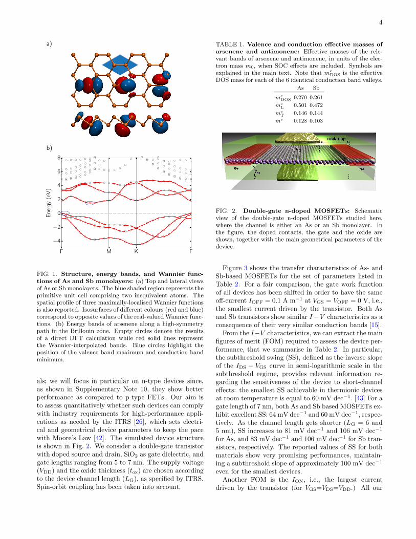
In Fig. 1a we show the equilibrium crystal struc-ture of arsenene and antimonene. Differently to phos-phorene, As and Sb monolayers are not puckered, butdisplay a buckled structure more similar to silicene orgermanene [29, 30], with two inequivalent atoms insidethe primitive hexagonal unit cell lying on two differentplanes. (Note that As and Sb have also been predictedto exist in a puckered structure, but this phase is en-
ergetically less favourable [13, 14]). The separation dbetween the planes reads 1.394 A for As and 1.640 A forSb, while the equilibrium lattice constant a is, respec-tively, 3.601 A and 4.122 A. The band structure of bothmaterials is very similar and in Fig. 1b we show the en-ergy bands along a high-symmetry path in the Brillouinzone obtained from DFT (empty circles) in the case ofarsenene (for the bands of antimonene see Supplemen-tary Figure 1). The DFT band gap is indirect (for bothmaterials) and equal to 1.48 eV for As and 1.00 eV forSb. The maximum of the valence bands is located atthe Γ point and, without SOC, it would be two-fold de-generate; the inclusion of the SOC splits the degeneracy(see Fig. 1b and Supplementary Figure 2) and the top-most valence band becomes non-degenerate, except forthe twofold spin degeneracy. The minimum of the con-duction bands lies instead along the Γ−M line and givesrise to six valleys.
Further analyses of the electronic properties of ar-senene and antimonene have been performed by firstmapping the Bloch eigenstates associated with the bandsaround the gap into a set of maximally localised Wan-nier functions[22]. We focused in particular on the threetop valence bands and three bottom conduction bands(per spin component). The main orbital contribution tothese bands comes from p-orbitals of the atoms that formbonding and antibonding combinations around the gap.By projecting over the p-orbitals of the two atoms in theprimitive cell, the standard localisation procedure leadsto six Wannier functions per spin component, three cen-tred on one atom and three on the other. In Fig. 1awe show the spatial profile of the three Wannier func-tions centred on atoms belonging to the lower plane (theother three can be obtained simply by spatial inversionthrough a mid-bond centre). They clearly have a p-likecharacter with minor contributions from neighbouringatoms. From the knowledge of these Wannier functionsit is straightforward to compute the matrix elements ofthe Hamiltonian between them.
In such a way, it becomes possible to interpolate ef-ficiently the Hamiltonian at any arbitrary k−point inreciprocal space, keeping the same accuracy of the un-derlying first-principles simulation, but at an extremelyreduced computational cost. In Fig. 1b we show theWannier-interpolated energy bands (red solid lines) witha much denser mesh than the original DFT results(empty circles) for As monolayer (bands for Sb mono-layer are shown in Supplementary Figure 1). Exploitingsuch interpolation scheme, we also computed the effectivemasses for relevant band extrema that crucially affectcarrier mobilities and intraband tunnelling amplitudes.We both fitted the electronic bands along principal di-rections and evaluated accurately the density-of-states(DOS) on an extremely dense grid. The values of themasses are reported in Table 1 for both materials. Inparticular, for the valence band maxima, the SOC splits
3
the degeneracy of the two topmost bands at Γ. Since themagnitude of the splitting is large, for realistic band fill-ing levels we can limit ourselves to consider only the top-most valence band, with (isotropic) mass mv. (If SOCwas neglected, we would need instead to consider bothdegenerate bands, as discussed in Supplementary Notes2–5 and Supplementary Figures 2–5.) For the conductionbands, the isoenergies of the six valleys are oblate witha larger effective mass mc
L in the longitudinal directionwith respect to the transverse effective mass mc
T. Theeffective DOS mass for each valley mc
DOS computed in-dependently is in agreement with what can be expectedfrom geometrical arguments, i.e. mc
DOS ≈√mc
LmcT.
As a first assessment of the material properties towardthe realisation of a transistor device using arsenene orantimonene as channel materials, we estimate whetherthe ballistic approximation is valid at room-temperature(T = 300 K) in the ultrascaled sub-10 nm regime that weinvestigate in this work. We will limit the analysis onlyto the intrinsic scattering with longitudinal acoustic (LA)phonons. As other scattering mechanisms may be activein the system, the values that we calculate should be con-sidered as upper limits to the actual scattering times or,equivalently, to the carrier mobility. In particular, whileout-of-plane (ZA) phonons may play an important rolein free-standing Dirac materials without planar symme-try [31, 32], we do not consider them here. While in afree-standing material scattering with ZA phonons canbe relevant, in our systems the device geometry (pres-ence of substrate and of top gates) will shift the ZAphonon modes at finite energy, reducing their impact onthe mobilities.[33]
While accurate values for the electron-phonon scatter-ing terms can be obtained fully ab-initio [34, 35], an ef-ficient method to get estimates for the scattering timesand mobilities relies on deformation-potential theory[36]and Fermi’s golden rule to estimate the scattering times.An estimate of the 2D mobility can be then obtainedusing Takagi’s formula [9, 37, 38]
µ2D =eh3C2D
kBTm∗emDOS(Ei)2, (1)
where m∗e is the transport effective mass, mDOS the DOSeffective mass (Table 1), kB the Boltzmann constant, Tthe temperature, Ei the deformation potential constant,and C2D the elastic modulus. In our case, we need toconsider this formula in the multi-valley, anisotropic case:details can be found in Supplementary Notes 3–9 anddescribed in Supplementary Figures 3–7, as well as thevalues of the extracted relevant parameters (deformationpotentials and elastic moduli, reported in SupplementaryTables 1 and 2, respectively).
We would like to emphasise, however, that this for-mula, while often adopted in the literature, cannot beused to obtain a quantitative estimate of the mobility. In-deed, the formula neglects the coupling with ZA phonons
(which may be important, as already discussed above), aswell as with TA and optical phonons. Moreover, it can-not fully capture the anisotropy of the electron-phononcoupling coefficients. A full ab-initio treatment of theelectron-phonon scattering is required, if a quantitativeestimation is needed (see e.g. discussions in Refs. 31 and39). Nevertheless, we provide here an estimate of whatwe will call hereafter Takagi’s mobilities, mainly to allowto compare As and Sb with other 2D materials alreadyinvestigated in the literature within the same level of the-ory. We have estimated that, in the worst case scenario,the values of actual mobilities could be reduced up to afactor of 8 when a full treatment of the electron-phononcoupling is adopted, including intervalley scattering.
The resulting values of the electron Takagi’s mo-bility µc and the hole Takagi’s mobility µh are 635and 1700 cm2V−1s−1, respectively, for As and 630 and1737 cm2V−1s−1 for Sb.
The values of the electron Takagi’s mobility are quitepromising and comparable with theoretical results forphosphorene using the same level of theory[9] and evenbetter than MoS2[40] owing to the smaller deforma-tion potential. The hole Takagi’s mobility is evenlarger, and in particular much larger than the exper-imentally measured value of the mobility in MoS2 atroom temperature[41] and in other 2D materials, likee.g. phosphorene[8]. On the other hand, we note thatour predicted values are smaller than those predicted bysimulations at the same level of theory (Takagi’s formula)for phosphorene[9], owing to the larger elastic modulusand smaller deformation potential in the zigzag direction.
We also emphasise that in arsenene and antimonenethe SOC effects are negligible for the conduction band.Instead, µh is significantly enhanced by the SOC, dueto the splitting of the topmost valence band and the re-sulting changes in the effective masses and deformationpotentials (see Supplementary Tables 1 to 3). In partic-ular, the inclusion of the SOC increases µh by 25% and84% in As and Sb, respectively (see Supplementary Table4).
From these values of the Takagi’s mobilities and the as-sociated scattering times and carrier velocities reportedin the Supplementary Note 10, we estimate that the meanfree path limited by LA phonons is of the order of tens ofnm. For this reason we assume that, for the dimensionsconsidered in this work, the use of the ballistic approxi-mation is justified and sets a higher limit to the perfor-mance achievable in these devices.
Performance of arsenene and antimonene baseddevices
In view of the results of the previous section, we per-form a full device simulation of field-effect transistorsbased on arsenene and antimonene as channel materi-
4
Γ M K Γ
−4
−2
0
2
4
6
8
Energy(eV)
a)
b)
FIG. 1. Structure, energy bands, and Wannier func-tions of As and Sb monolayers: (a) Top and lateral viewsof As or Sb monolayers. The blue shaded region represents theprimitive unit cell comprising two inequivalent atoms. Thespatial profile of three maximally-localised Wannier functionsis also reported. Isosurfaces of different colours (red and blue)correspond to opposite values of the real-valued Wannier func-tions. (b) Energy bands of arsenene along a high-symmetrypath in the Brillouin zone. Empty circles denote the resultsof a direct DFT calculation while red solid lines representthe Wannier-interpolated bands. Blue circles highlight theposition of the valence band maximum and conduction bandminimum.
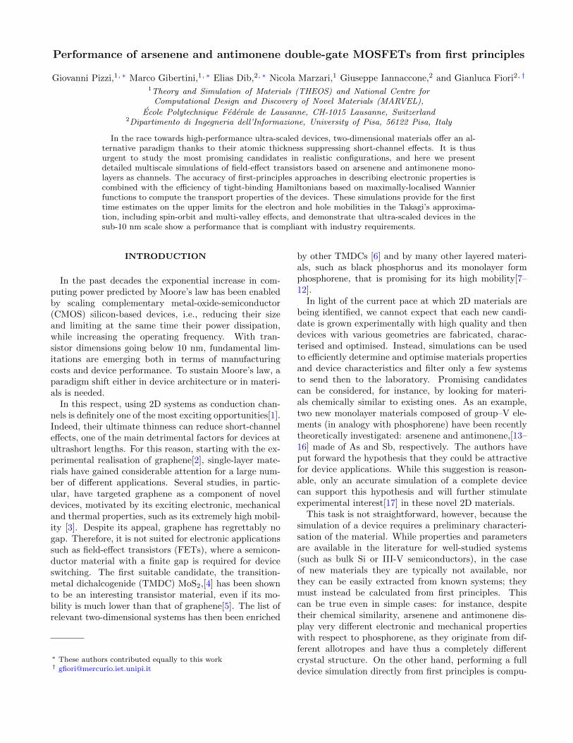
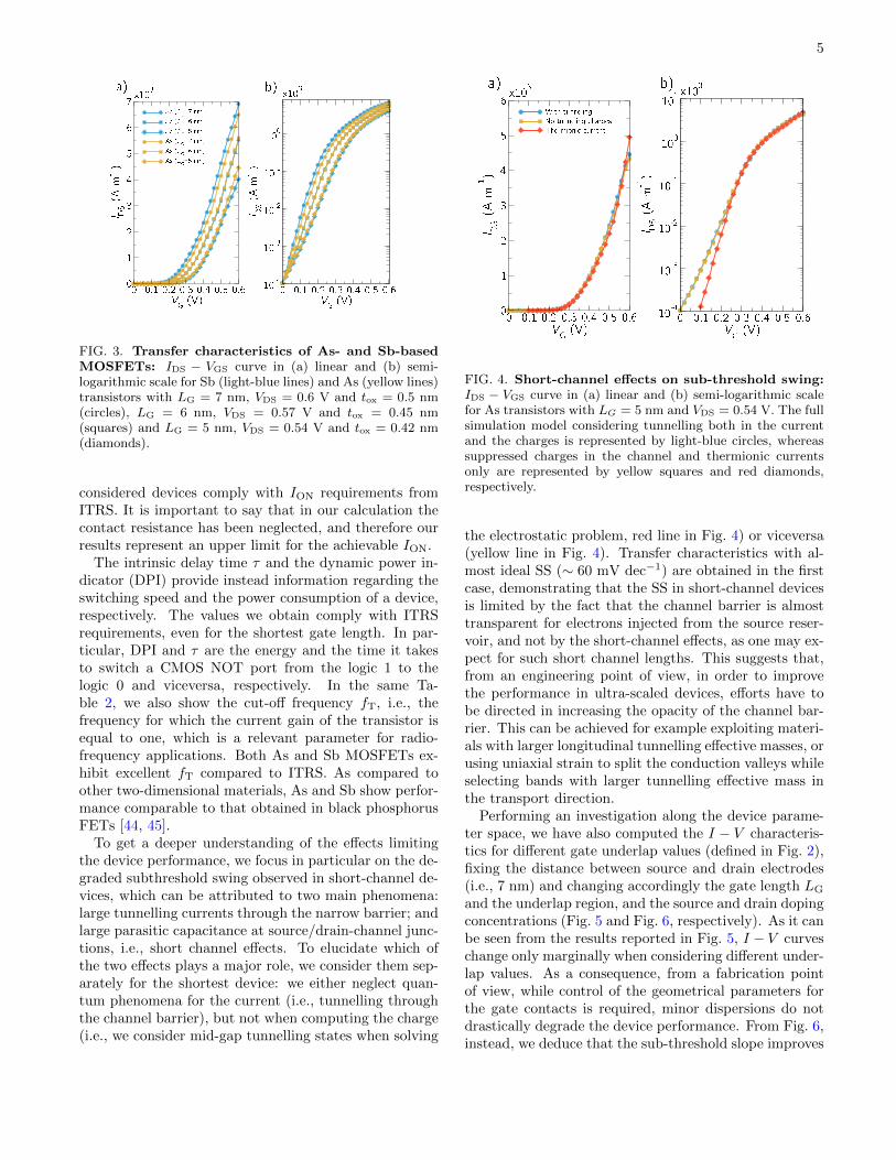
als; we will focus in particular on n-type devices since,as shown in Supplementary Note 10, they show betterperformance as compared to p-type FETs. Our aim isto assess quantitatively whether such devices can complywith industry requirements for high-performance appli-cations as needed by the ITRS [26], which sets electri-cal and geometrical device parameters to keep the pacewith Moore’s Law [42]. The simulated device structureis shown in Fig. 2. We consider a double-gate transistorwith doped source and drain, SiO2 as gate dielectric, andgate lengths ranging from 5 to 7 nm. The supply voltage(VDD) and the oxide thickness (tox) are chosen accordingto the device channel length (LG), as specified by ITRS.Spin-orbit coupling has been taken into account.
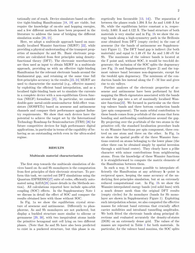
TABLE 1. Valence and conduction effective masses ofarsenene and antimonene: Effective masses of the rele-vant bands of arsenene and antimonene, in units of the elec-tron mass m0, when SOC effects are included. Symbols areexplained in the main text. Note that mc
DOS is the effectiveDOS mass for each of the 6 identical conduction band valleys.
As Sb
mcDOS 0.270 0.261
mcL 0.501 0.472
mcT 0.146 0.144
mv 0.128 0.103
FIG. 2. Double-gate n-doped MOSFETs: Schematicview of the double-gate n-doped MOSFETs studied here,where the channel is either an As or an Sb monolayer. Inthe figure, the doped contacts, the gate and the oxide areshown, together with the main geometrical parameters of thedevice.
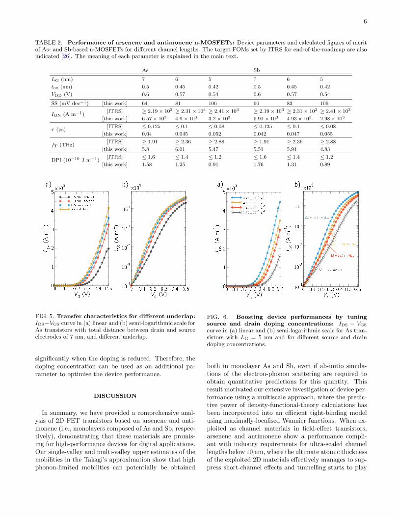
Figure 3 shows the transfer characteristics of As- andSb-based MOSFETs for the set of parameters listed inTable 2. For a fair comparison, the gate work functionof all devices has been shifted in order to have the sameoff-current IOFF = 0.1 A m−1 at VGS = VOFF = 0 V, i.e.,the smallest current driven by the transistor. Both Asand Sb transistors show similar I−V characteristics as aconsequence of their very similar conduction bands [15].
From the I−V characteristics, we can extract the mainfigures of merit (FOM) required to assess the device per-formance, that we summarise in Table 2. In particular,the subthreshold swing (SS), defined as the inverse slopeof the IDS − VGS curve in semi-logarithmic scale in thesubthreshold regime, provides relevant information re-garding the sensitiveness of the device to short-channeleffects: the smallest SS achievable in thermionic devicesat room temperature is equal to 60 mV dec−1. [43] For agate length of 7 nm, both As and Sb based MOSFETs ex-hibit excellent SS: 64 mV dec−1 and 60 mV dec−1, respec-tively. As the channel length gets shorter (LG = 6 and5 nm), SS increases to 81 mV dec−1 and 106 mV dec−1
for As, and 83 mV dec−1 and 106 mV dec−1 for Sb tran-sistors, respectively. The reported values of SS for bothmaterials show very promising performances, maintain-ing a subthreshold slope of approximately 100 mV dec−1
even for the smallest devices.Another FOM is the ION, i.e., the largest current
driven by the transistor (for VGS=VDS=VDD.) All our
5
FIG. 3. Transfer characteristics of As- and Sb-basedMOSFETs: IDS − VGS curve in (a) linear and (b) semi-logarithmic scale for Sb (light-blue lines) and As (yellow lines)transistors with LG = 7 nm, VDS = 0.6 V and tox = 0.5 nm(circles), LG = 6 nm, VDS = 0.57 V and tox = 0.45 nm(squares) and LG = 5 nm, VDS = 0.54 V and tox = 0.42 nm(diamonds).
considered devices comply with ION requirements fromITRS. It is important to say that in our calculation thecontact resistance has been neglected, and therefore ourresults represent an upper limit for the achievable ION.
The intrinsic delay time τ and the dynamic power in-dicator (DPI) provide instead information regarding theswitching speed and the power consumption of a device,respectively. The values we obtain comply with ITRSrequirements, even for the shortest gate length. In par-ticular, DPI and τ are the energy and the time it takesto switch a CMOS NOT port from the logic 1 to thelogic 0 and viceversa, respectively. In the same Ta-ble 2, we also show the cut-off frequency fT, i.e., thefrequency for which the current gain of the transistor isequal to one, which is a relevant parameter for radio-frequency applications. Both As and Sb MOSFETs ex-hibit excellent fT compared to ITRS. As compared toother two-dimensional materials, As and Sb show perfor-mance comparable to that obtained in black phosphorusFETs [44, 45].
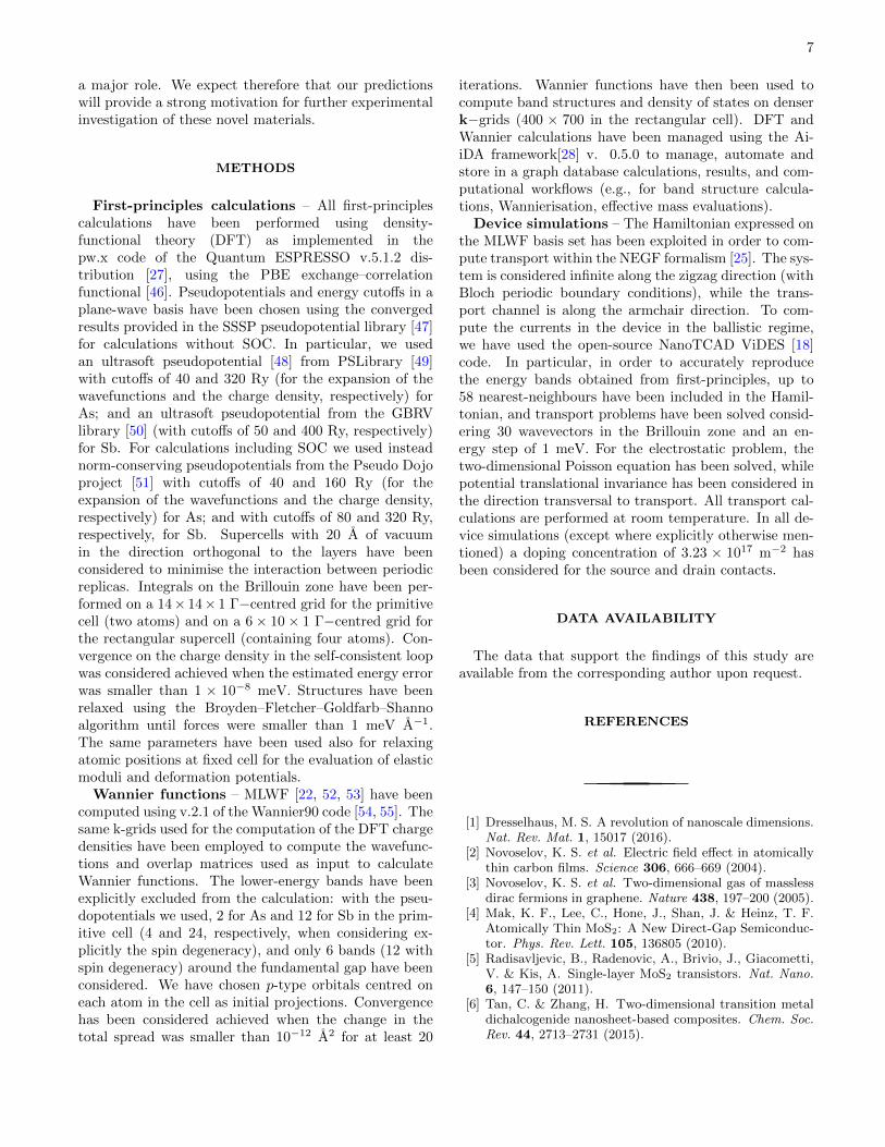
To get a deeper understanding of the effects limitingthe device performance, we focus in particular on the de-graded subthreshold swing observed in short-channel de-vices, which can be attributed to two main phenomena:large tunnelling currents through the narrow barrier; andlarge parasitic capacitance at source/drain-channel junc-tions, i.e., short channel effects. To elucidate which ofthe two effects plays a major role, we consider them sep-arately for the shortest device: we either neglect quan-tum phenomena for the current (i.e., tunnelling throughthe channel barrier), but not when computing the charge(i.e., we consider mid-gap tunnelling states when solving
FIG. 4. Short-channel effects on sub-threshold swing:IDS − VGS curve in (a) linear and (b) semi-logarithmic scalefor As transistors with LG = 5 nm and VDS = 0.54 V. The fullsimulation model considering tunnelling both in the currentand the charges is represented by light-blue circles, whereassuppressed charges in the channel and thermionic currentsonly are represented by yellow squares and red diamonds,respectively.
the electrostatic problem, red line in Fig. 4) or viceversa(yellow line in Fig. 4). Transfer characteristics with al-most ideal SS (∼ 60 mV dec−1) are obtained in the firstcase, demonstrating that the SS in short-channel devicesis limited by the fact that the channel barrier is almosttransparent for electrons injected from the source reser-voir, and not by the short-channel effects, as one may ex-pect for such short channel lengths. This suggests that,from an engineering point of view, in order to improvethe performance in ultra-scaled devices, efforts have tobe directed in increasing the opacity of the channel bar-rier. This can be achieved for example exploiting materi-als with larger longitudinal tunnelling effective masses, orusing uniaxial strain to split the conduction valleys whileselecting bands with larger tunnelling effective mass inthe transport direction.
Performing an investigation along the device parame-ter space, we have also computed the I − V characteris-tics for different gate underlap values (defined in Fig. 2),fixing the distance between source and drain electrodes(i.e., 7 nm) and changing accordingly the gate length LG
and the underlap region, and the source and drain dopingconcentrations (Fig. 5 and Fig. 6, respectively). As it canbe seen from the results reported in Fig. 5, I − V curveschange only marginally when considering different under-lap values. As a consequence, from a fabrication pointof view, while control of the geometrical parameters forthe gate contacts is required, minor dispersions do notdrastically degrade the device performance. From Fig. 6,instead, we deduce that the sub-threshold slope improves
6
TABLE 2. Performance of arsenene and antimonene n-MOSFETs: Device parameters and calculated figures of meritof As- and Sb-based n-MOSFETs for different channel lengths. The target FOMs set by ITRS for end-of-the-roadmap are alsoindicated [26]. The meaning of each parameter is explained in the main text.
As Sb
LG (nm) 7 6 5 7 6 5
tox (nm) 0.5 0.45 0.42 0.5 0.45 0.42
VDD (V) 0.6 0.57 0.54 0.6 0.57 0.54
SS (mV dec−1) [this work] 64 81 106 60 83 106
ION (A m−1)[ITRS] ≥ 2.19 × 10³ ≥ 2.31 × 10³ ≥ 2.41 × 10³ ≥ 2.19 × 10³ ≥ 2.31 × 10³ ≥ 2.41 × 10³
[this work] 6.57 × 10³ 4.9 × 10³ 3.2 × 10³ 6.91 × 10³ 4.93 × 10³ 2.98 × 10³
τ (ps)[ITRS] ≤ 0.125 ≤ 0.1 ≤ 0.08 ≤ 0.125 ≤ 0.1 ≤ 0.08
[this work] 0.04 0.045 0.052 0.042 0.047 0.055
fT (THz)[ITRS] ≥ 1.91 ≥ 2.36 ≥ 2.88 ≥ 1.91 ≥ 2.36 ≥ 2.88
[this work] 5.8 6.01 5.47 5.51 5.94 4.83
DPI (10−10 J m−1)[ITRS] ≤ 1.6 ≤ 1.4 ≤ 1.2 ≤ 1.6 ≤ 1.4 ≤ 1.2
[this work] 1.58 1.25 0.91 1.76 1.31 0.89
FIG. 5. Transfer characteristics for different underlap:IDS−VGS curve in (a) linear and (b) semi-logarithmic scale forAs transistors with total distance between drain and sourceelectrodes of 7 nm, and different underlap.
significantly when the doping is reduced. Therefore, thedoping concentration can be used as an additional pa-rameter to optimise the device performance.
DISCUSSION
In summary, we have provided a comprehensive anal-ysis of 2D FET transistors based on arsenene and anti-monene (i.e., monolayers composed of As and Sb, respec-tively), demonstrating that these materials are promis-ing for high-performance devices for digital applications.Our single-valley and multi-valley upper estimates of themobilities in the Takagi’s approximation show that highphonon-limited mobilities can potentially be obtained
FIG. 6. Boosting device performances by tuningsource and drain doping concentrations: IDS − VGS
curve in (a) linear and (b) semi-logarithmic scale for As tran-sistors with LG = 5 nm and for different source and draindoping concentrations.
both in monolayer As and Sb, even if ab-initio simula-tions of the electron-phonon scattering are required toobtain quantitative predictions for this quantity. Thisresult motivated our extensive investigation of device per-formance using a multiscale approach, where the predic-tive power of density-functional-theory calculations hasbeen incorporated into an efficient tight-binding modelusing maximally-localised Wannier functions. When ex-ploited as channel materials in field-effect transistors,arsenene and antimonene show a performance compli-ant with industry requirements for ultra-scaled channellengths below 10 nm, where the ultimate atomic thicknessof the exploited 2D materials effectively manages to sup-press short-channel effects and tunnelling starts to play
7
a major role. We expect therefore that our predictionswill provide a strong motivation for further experimentalinvestigation of these novel materials.
METHODS
First-principles calculations – All first-principlescalculations have been performed using density-functional theory (DFT) as implemented in thepw.x code of the Quantum ESPRESSO v.5.1.2 dis-tribution [27], using the PBE exchange–correlationfunctional [46]. Pseudopotentials and energy cutoffs in aplane-wave basis have been chosen using the convergedresults provided in the SSSP pseudopotential library [47]for calculations without SOC. In particular, we usedan ultrasoft pseudopotential [48] from PSLibrary [49]with cutoffs of 40 and 320 Ry (for the expansion of thewavefunctions and the charge density, respectively) forAs; and an ultrasoft pseudopotential from the GBRVlibrary [50] (with cutoffs of 50 and 400 Ry, respectively)for Sb. For calculations including SOC we used insteadnorm-conserving pseudopotentials from the Pseudo Dojoproject [51] with cutoffs of 40 and 160 Ry (for theexpansion of the wavefunctions and the charge density,respectively) for As; and with cutoffs of 80 and 320 Ry,respectively, for Sb. Supercells with 20 A of vacuumin the direction orthogonal to the layers have beenconsidered to minimise the interaction between periodicreplicas. Integrals on the Brillouin zone have been per-formed on a 14× 14× 1 Γ−centred grid for the primitivecell (two atoms) and on a 6 × 10 × 1 Γ−centred grid forthe rectangular supercell (containing four atoms). Con-vergence on the charge density in the self-consistent loopwas considered achieved when the estimated energy errorwas smaller than 1 × 10⁻⁸ meV. Structures have beenrelaxed using the Broyden–Fletcher–Goldfarb–Shannoalgorithm until forces were smaller than 1 meV A−1.The same parameters have been used also for relaxingatomic positions at fixed cell for the evaluation of elasticmoduli and deformation potentials.
Wannier functions – MLWF [22, 52, 53] have beencomputed using v.2.1 of the Wannier90 code [54, 55]. Thesame k-grids used for the computation of the DFT chargedensities have been employed to compute the wavefunc-tions and overlap matrices used as input to calculateWannier functions. The lower-energy bands have beenexplicitly excluded from the calculation: with the pseu-dopotentials we used, 2 for As and 12 for Sb in the prim-itive cell (4 and 24, respectively, when considering ex-plicitly the spin degeneracy), and only 6 bands (12 withspin degeneracy) around the fundamental gap have beenconsidered. We have chosen p-type orbitals centred oneach atom in the cell as initial projections. Convergencehas been considered achieved when the change in thetotal spread was smaller than 10−12 A2 for at least 20
iterations. Wannier functions have then been used tocompute band structures and density of states on denserk−grids (400 × 700 in the rectangular cell). DFT andWannier calculations have been managed using the Ai-iDA framework[28] v. 0.5.0 to manage, automate andstore in a graph database calculations, results, and com-putational workflows (e.g., for band structure calcula-tions, Wannierisation, effective mass evaluations).Device simulations – The Hamiltonian expressed on
the MLWF basis set has been exploited in order to com-pute transport within the NEGF formalism [25]. The sys-tem is considered infinite along the zigzag direction (withBloch periodic boundary conditions), while the trans-port channel is along the armchair direction. To com-pute the currents in the device in the ballistic regime,we have used the open-source NanoTCAD ViDES [18]code. In particular, in order to accurately reproducethe energy bands obtained from first-principles, up to58 nearest-neighbours have been included in the Hamil-tonian, and transport problems have been solved consid-ering 30 wavevectors in the Brillouin zone and an en-ergy step of 1 meV. For the electrostatic problem, thetwo-dimensional Poisson equation has been solved, whilepotential translational invariance has been considered inthe direction transversal to transport. All transport cal-culations are performed at room temperature. In all de-vice simulations (except where explicitly otherwise men-tioned) a doping concentration of 3.23 × 10¹⁷ m−2 hasbeen considered for the source and drain contacts.
DATA AVAILABILITY
The data that support the findings of this study areavailable from the corresponding author upon request.
REFERENCES
[1] Dresselhaus, M. S. A revolution of nanoscale dimensions.Nat. Rev. Mat. 1, 15017 (2016).
[2] Novoselov, K. S. et al. Electric field effect in atomicallythin carbon films. Science 306, 666–669 (2004).
[3] Novoselov, K. S. et al. Two-dimensional gas of masslessdirac fermions in graphene. Nature 438, 197–200 (2005).
[4] Mak, K. F., Lee, C., Hone, J., Shan, J. & Heinz, T. F.Atomically Thin MoS2: A New Direct-Gap Semiconduc-tor. Phys. Rev. Lett. 105, 136805 (2010).
[5] Radisavljevic, B., Radenovic, A., Brivio, J., Giacometti,V. & Kis, A. Single-layer MoS2 transistors. Nat. Nano.6, 147–150 (2011).
[6] Tan, C. & Zhang, H. Two-dimensional transition metaldichalcogenide nanosheet-based composites. Chem. Soc.Rev. 44, 2713–2731 (2015).
8
[7] Li, L. et al. Black phosphorus field-effect transistors. Nat.Nano. 9, 372–377 (2014).
[8] Liu, H. et al. Phosphorene: An Unexplored 2D Semicon-ductor with a High Hole Mobility. ACS Nano 8, 4033–4041 (2014).
[9] Qiao, J., Kong, X., Hu, Z.-X., Yang, F. & Ji, W. High-mobility transport anisotropy and linear dichroism infew-layer black phosphorus. Nat. Commun. 5, 4475(2014).
[10] Wang, H. et al. Black phosphorus radio-frequency tran-sistors. Nano Letters 14, 6424–6429 (2014).
[11] Du, Y., Liu, H., Deng, Y. & Ye, P. D. Device perspectivefor black phosphorus field-effect transistors: Contact re-sistance, ambipolar behavior, and scaling. ACS Nano 8,10035–10042 (2014).
[12] Avsar, A. et al. Air-stable transport in graphene-contacted, fully encapsulated ultrathin blackphosphorus-based field-effect transistors. ACS Nano 9,4138–4145 (2015).
[13] Kamal, C. & Ezawa, M. Arsenene: Two-dimensionalbuckled and puckered honeycomb arsenic systems. Phys.Rev. B 91, 085423 (2015).
[14] Wang, G., Pandey, R. & Karna, S. P. Atomically ThinGroup V Elemental Films: Theoretical Investigations ofAntimonene Allotropes. ACS Appl. Mater. Interfaces 7,11490–11496 (2015).
[15] Zhang, S., Yan, Z., Li, Y., Chen, Z. & Zeng, H.Atomically thin arsenene and antimonene: Semimetal–semiconductor and indirect–direct band-gap transitions.Angew. Chem. Int. Ed. 54, 3112–3115 (2015).
[16] Zhu, Z., Guan, J. & Tomanek, D. Strain-induced metal-semiconductor transition in monolayers and bilayers ofgray arsenic: A computational study. Phys. Rev. B 91,161404 (2015).
[17] Lei, T. et al. Electronic structure of antimonene grownon Sb2Te3 (111) and Bi2Te3 substrates. J. Appl. Phys.119, 015302 (2016).
[18] NanoTCAD ViDES (2015). URL http://vides.
nanotcad.com.[19] Fiori, G. & Iannaccone, G. Multiscale modeling for
graphene-based nanoscale transistors. Proc. IEEE 101,1653–1669 (2013).
[20] Porezag, D., Frauenheim, T., Kohler, T., Seifert, G. &Kaschner, R. Construction of tight-binding-like poten-tials on the basis of density-functional theory: Applica-tion to carbon. Phys. Rev. B 51, 12947–12957 (1995).
[21] Tan, Y. et al. Empirical tight binding parameters forGaAs and MgO with explicit basis through DFT map-ping. J. Comp. Electron. 12, 56–60 (2013).
[22] Marzari, N., Mostofi, A. A., Yates, J. R., Souza, I. &Vanderbilt, D. Maximally localized Wannier functions:Theory and applications. Rev. Mod. Phys. 84, 1419–1475(2012).
[23] Lee, Y.-S., Nardelli, M. B. & Marzari, N. Band Struc-ture and Quantum Conductance of Nanostructures fromMaximally Localized Wannier Functions: The Case ofFunctionalized Carbon Nanotubes. Phys. Rev. Lett. 95,076804 (2005).
[24] Bruzzone, S., Iannaccone, G., Marzari, N. & Fiori, G.An open-source multiscale framework for the simulationof nanoscale devices. IEEE Trans. Electron Devices 61,48–53 (2014).
[25] Datta, S. Electronic Transport in Mesoscopic Systems,1st edn. (Cambridge University Press, 1995).
[26] The International Techonology Roadmap for Semicon-ductors (2011). URL http://www.itrs2.net.
[27] Giannozzi, P. et al. QUANTUM ESPRESSO: a modularand open-source software project for quantum simula-tions of materials. J. Phys. Condens. Matter 21, 395502(2009).
[28] Pizzi, G., Cepellotti, A., Sabatini, R., Marzari, N. &Kozinsky, B. AiiDA: automated interactive infrastruc-ture and database for computational science. Comp. Mat.Sci. 111, 218–230 (2016).
[29] Aufray, B. et al. Graphene-like silicon nanoribbons onAg(110): A possible formation of silicene. Appl. Phys.Lett. 96, 183102 (2010).
[30] Davila, M. E., Xian, L., Cahangirov, S., Rubio, A. &Le Lay, G. Germanene: a novel two-dimensional germa-nium allotrope akin to graphene and silicene. New J.Phys. 16, 095002 (2014).
[31] Fischetti, M. V. & Vandenberghe, W. G. Mermin-wagnertheorem, flexural modes, and degraded carrier mobilityin two-dimensional crystals with broken horizontal mirrorsymmetry. Phys. Rev. B 93, 155413 (2016).
[32] Gunst, T., Markussen, T., Stokbro, K. & Brandbyge,M. First-principles method for electron-phonon couplingand electron mobility: Applications to two-dimensionalmaterials. Phys. Rev. B 93, 035414 (2016).
[33] Slotman, G. J., de Wijs, G. A., Fasolino, A. & Kat-snelson, M. I. Phonons and electron-phonon couplingin graphene-h-BN heterostructures. Annalen Der Physik526, 381–386 (2014).
[34] Savrasov, S. Y., Savrasov, D. Y. & Andersen, O. K.Linear-response calculations of electron-phonon interac-tions. Phys. Rev. Lett. 72, 372–375 (1994).
[35] Giustino, F., Cohen, M. L. & Louie, S. G. Electron-phonon interaction using Wannier functions. Phys. Rev.B 76, 165108 (2007).
[36] Bardeen, J. & Shockley, W. Deformation potentials andmobilities in non-polar crystals. Phys. Rev. 80, 72–80(1950).
[37] Takagi, S., Toriumi, A., Iwase, M. & Tango, H. On theuniversality of inversion layer mobility in Si MOSFET’s:Part II-effects of surface orientation. IEEE Trans. Elec-tron Devices 41, 2363–2368 (1994).
[38] Xi, J., Long, M., Tang, L., Wang, D. & Shuai, Z. First-principles prediction of charge mobility in carbon andorganic nanomaterials. Nanoscale 4, 4348–4369 (2012).
[39] Liao, B., Zhou, J., Qiu, B., Dresselhaus, M. S. & Chen,G. Ab initio study of electron-phonon interaction in phos-phorene. Phys. Rev. B 91, 235419 (2015).
[40] Cai, Y., Zhang, G. & Zhang, Y.-W. Polarity-ReversedRobust Carrier Mobility in Monolayer MoS2 Nanorib-bons. J. Am. Chem. Soc. 136, 6269–6275 (2014).
[41] Radisavljevic, B. & Kis, A. Reply to ‘Measurement ofmobility in dual-gated MoS2 transistors’. Nat. Nano. 8,147–148 (2013).
[42] Moore, G. Cramming more components onto integratedcircuits. Electron. Mag. 38, 114–117 (1965).
[43] Taur, Y. & H., N. T. Fundamentals of modern VLSIdevices, 1st edn. (Cambridge University Press, 2001).
[44] Lam, K. T., Dong, Z. & Guo, J. Performance limitsprojection of black phosphorous field-effect transistors.IEEE Electron Device Letters 35, 963–965 (2014).
[45] Liu, F., Wang, Y., Liu, X., Wang, J. & Guo, H. Ballis-tic transport in monolayer black phosphorus transistors.IEEE Trans. Electron Devices 61, 3871–3876 (2014).
9
[46] Perdew, J. P., Burke, K. & Ernzerhof, M. Generalizedgradient approximation made simple. Phys. Rev. Lett.77, 3865–3868 (1996).
[47] Standard Solid State Pseudopotentials (SSSP) (2015).URL http://www.materialscloud.org/sssp.
[48] Vanderbilt, D. Soft self-consistent pseudopotentials ina generalized eigenvalue formalism. Phys. Rev. B 41,7892–7895 (1990).
[49] Dal Corso, A. Pseudopotentials periodic table: From Hto Pu. Comp. Mat. Sci. 95, 337–350 (2014).
[50] Garrity, K. F., Bennett, J. W., Rabe, K. M. & Van-derbilt, D. Pseudopotentials for high-throughput DFTcalculations. Comp. Mat. Sci. 81, 446–452 (2014).
[51] Pseudo Dojo (2016). URL http://www.pseudo-dojo.
org.[52] Marzari, N. & Vanderbilt, D. Maximally localized gen-
eralized Wannier functions for composite energy bands.Phys. Rev. B 56, 12847–12865 (1997).
[53] Souza, I., Marzari, N. & Vanderbilt, D. Maximally local-ized Wannier functions for entangled energy bands. Phys.Rev. B 65, 035109 (2001).
[54] Mostofi, A. A. et al. wannier90: A tool for obtain-ing maximally-localised Wannier functions. Comp. Phys.Comm. 178, 685–699 (2008).
[55] Mostofi, A. A. et al. An updated version of wannier90:A tool for obtaining maximally-localised Wannier func-tions. Comp. Phys. Comm. 185, 2309–2310 (2014).
ACKNOWLEDGEMENTS
We thank Nicolas Mounet for providing us with the Ai-iDA workflow to compute band structures with QuantumESPRESSO and Massimo Fischetti for very insightfuldiscussions. This work was supported by a grant from theSwiss National Supercomputing Centre (CSCS) underproject IDs s580. M.G., N.M., G.I. and G.F. gratefullyacknowledge the Graphene Flagship (contract 604391).
AUTHOR CONTRIBUTIONS
G.P., M.G. and G.F. conceived the work; G.P. andM.G. performed first-principles and Wannier simulationsunder the supervision of N.M.; E.D. performed theNEGF device simulations under the supervision of G.I.and G.F; all authors analysed the results and wrote thepaper.
Competing financial interests
The authors declare no competing financial interests.