


Performance Enhancing Nano Coatings: Changing … Recommend new area ratio (SAR) guidelines for...
41
Performance Enhancing Nano Coatings: Changing the Rules of Stencil Design Tony Lentz [email protected]
-
Upload
trinhnguyet -
Category
Documents
-
view
224 -
download
2
Transcript of Performance Enhancing Nano Coatings: Changing … Recommend new area ratio (SAR) guidelines for...

Performance Enhancing
Nano Coatings:
Changing the Rules of Stencil Design
Tony Lentz

Outline/Agenda
Introduction
Experimental Design
Results of Experiment
Conclusions
Acknowledgements
Q & A
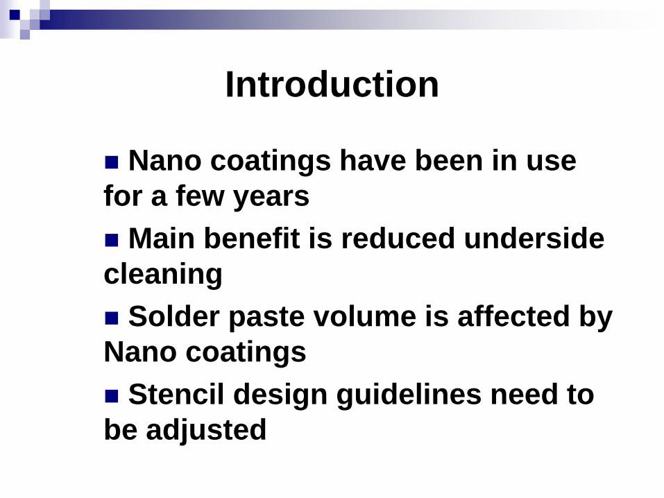
Introduction
Nano coatings have been in use
for a few years
Main benefit is reduced underside
cleaning
Solder paste volume is affected by
Nano coatings
Stencil design guidelines need to
be adjusted

Introduction

Introduction*
Nano
Coating
Application Chemistry Surface
Function
Aperture
Function
Coating B Wipe on Self assembled
monolayer
Cleaning
benefit
Reduced
paste volume
Coating C Wipe on Self assembled
monolayer
Cleaning
benefit
Reduced
paste volume
Coating D Spray on Thermal cure
polymer
Cleaning
benefit
Increased
paste volume
*SMTAI 2013, Can Nano-Coatings Really Improve Stencil Performance. T.
Lentz
Note: Coating A was not evaluated in this experiment

Miniaturization Trends*
*Murata Manufacturing Company
http://www.murata.com/products/article/pp09e1/3.html

Goals
Recommend new area ratio (SAR)
guidelines for stencil design
Give adjusted guidelines based on
solder paste type
Show how these guidelines
change when Nano coatings are
used

Experimental Design
10 circuit board print study
No underside cleaning
6 different solder pastes
Water soluble vs. no clean
Leaded vs. lead-free
Type 3, 4, and 5 solder powders
3 Nano-coated stencils vs.
uncoated stencil

Experimental Design
Essemtec printer
20 mm/sec, 0.18 Kg/cm, 1.5 mm/sec
ASC International SPI
AP212 with VM150 sensor
Stencils, 304 SS, 8-9 µm grain
0.005” (127 microns) thick
Circuit board, copper clad FR-4
0.059” thick, 0.5/0.5 oz. copper, 6.0” x 3.75”

Experimental Design

Experimental Design
Experimental Design
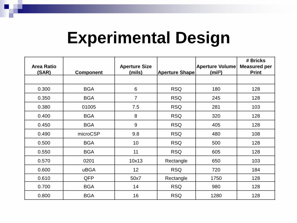
Area Ratio
(SAR) Component
Aperture Size
(mils) Aperture Shape
Aperture Volume
(mil3)
# Bricks
Measured per
0.300 BGA 6 RSQ 180 128
0.350 BGA 7 RSQ 245 128
0.380 01005 7.5 RSQ 281 103
0.400 BGA 8 RSQ 320 128
0.450 BGA 9 RSQ 405 128
0.490 microCSP 9.8 RSQ 480 108
0.500 BGA 10 RSQ 500 128
0.550 BGA 11 RSQ 605 128
0.570 0201 10x13 Rectangle 650 103
0.600 uBGA 12 RSQ 720 184
0.610 QFP 50x7 Rectangle 1750 128
0.700 BGA 14 RSQ 980 128
0.800 BGA 16 RSQ 1280 128

Experimental Design
*Successful Stencil Printing: Performance is on the Surface
Robert Dervaes, FCT Assembly

Experimental Design
Transfer Efficiency = [(measured paste volume) / (aperture volume)] x 100%
BGA
0.30 SAR

Results of Experiment
Nano coating effects
Solder powder variation T3, T4, T5
No clean vs. water soluble pastes
Leaded vs. lead-free pastes

Nano Coating Effects
Solder paste: No Clean SAC305 Type 3

Nano Coating Effects
Solder paste: No Clean SAC305 Type 3 (All SARs)

Nano Coating Effects
Solder paste: No Clean SAC305 Type 4

Nano Coating Effects
Solder paste: No Clean SAC305 Type 4 (All SARs)

Nano Coating Effects
Solder paste: No Clean SAC305 Type 5

Nano Coating Effects
Solder paste: No Clean SAC305 Type 5 (All SARs)

Nano Coating Effects
Solder paste: No Clean SAC305 Type 3 (All SARs)

Nano Coating Effects
Solder paste: No Clean SAC305 Type 3 CV = St Dev / Mean

Nano Coating Effects
Solder paste: No Clean SAC305 Type 3
Nano Coating Mean Transfer
Efficiency (%)
Mean
Coefficient of
Variation (%)
Uncoated 59 6.4
Coating B 58 6.9
Coating C 60 7.7
Coating D 71 7.1

Nano Coating Effects
Nano Coatings B and C have a
small effect on TE%
Nano Coating D gives an increase
in TE%
CV increased slightly by all nano
coatings, but all < 10%
Print to print variation was
reduced by Coating D
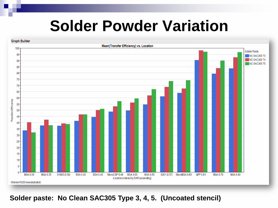
Solder Powder Variation
Solder paste: No Clean SAC305 Type 3, 4, 5. (Uncoated stencil)

Solder Powder Variation
Solder paste: No Clean SAC305 Type 3, 4, 5. (Uncoated stencil)

Solder Powder Variation
Type 4 & 5 TE% greater than T3
~9% TE increase from T3 to T4
Overall average TE% shows
similar performance for Type 4 & 5

Solder Paste Effects
Solder paste: All Type 3. (Uncoated stencil)

Solder Paste Effects
Solder paste: All Type 3. (Uncoated stencil, all SARs)
Solder Paste Effects
No cleans gave higher TE% than
water solubles
Lead free TE% > leaded
Paste chemistry & alloy affect
TE%

Stencil Design Rules
This does not account for stencil thickness, paste chemistry, or
Nano coatings
IPC-7525B 2011-October. Stencil Design Guidelines
3.2.1 Aperture Size. A typical guideline is a minimum of 4 to 5 particles of paste
powder across the width of an aperture.
Type Mesh Size (um) Size (mil)
Min Aperture
Size (mil)
2 -200/+325 45 - 75 1.8 - 3.0 15.0
3 -325/+500 25 - 45 1.0 - 1.8 9.0
4 -400/+635 20 - 38 0.8 - 1.5 7.5
5 -500/+800 15 - 25 0.6 - 1.0 5.0
Stencil Design Rules
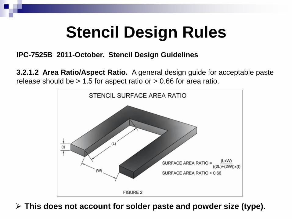
This does not account for solder paste and powder size (type).
IPC-7525B 2011-October. Stencil Design Guidelines
3.2.1.2 Area Ratio/Aspect Ratio. A general design guide for acceptable paste
release should be > 1.5 for aspect ratio or > 0.66 for area ratio.
Stencil Design Rules
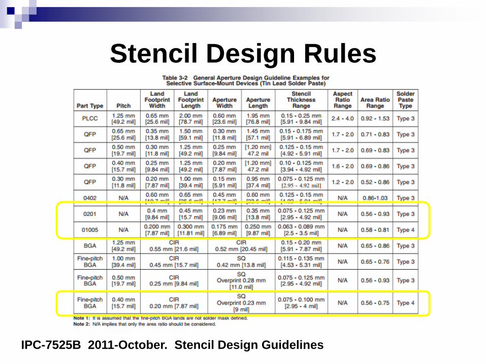
IPC-7525B 2011-October. Stencil Design Guidelines
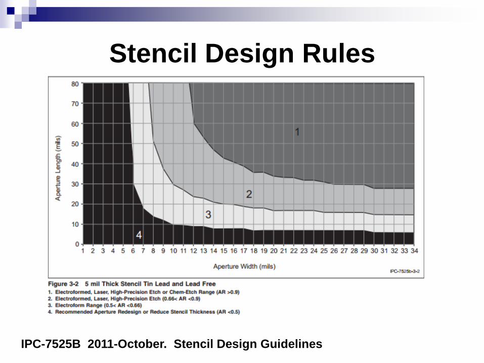
Stencil Design Rules
IPC-7525B 2011-October. Stencil Design Guidelines

Stencil Design Rules
Solder Paste Uncoated Coating B Coating C Coating D
NC SAC T3 0.61 0.61 0.61 0.55
NC SAC T4 0.61 0.61 0.61 0.49
NC SAC T5 0.57 0.57 0.57 0.45
WS SAC T3 0.70 ND ND 0.61
Minimum SAR Allowing 70% Solder Paste Volume
Variables Affecting
Solder Paste Release
Stencil design
Stencil to PWB registration
PWB (finish, pad size, etc.)
Printer parameters
Environmental conditions
Solder paste chemistry and powder
Nano coatings

Conclusions
Stencil design rules depend upon:
Aperture surface area ratio
Solder paste chemistry
Solder powder size (type)
Nano coating effect
Certain Nano coatings can change
the rules of stencil design

Acknowledgements
This study would not have been possible without the
assistance of Fine Line Stencil.
Many thanks to Brittney Nolan of FCT Assembly who
ran much of the testing for this study.


