Performance characterization of a DRAM-NVM hybrid memory ...
16
Performance characterization of a DRAM-NVM hybrid memory architecture for HPC applications using Intel Optane DC Persistent Memory Modules Onkar Patil 1 , Latchesar Ionkov 2 , Jason Lee 2 , Frank Mueller 1 , Michael Lang 2 1 North Carolina State University 2 Los Alamos National Laboratory [email protected] [email protected] lionkov,jasonlee,[email protected] Abstract Non-volatile, byte-addressable memory (NVM) has been introduced by Intel in the form of NVDIMMs named Intel ® Optane™ DC PMM. This memory module has the ability to persist the data stored in it without the need for power. This expands the memory hierarchy into a hybrid memory system due the differences in access latency and memory bandwidth from DRAM, which has been the predominant byte-addressable main memory technology. The Optane DC memory modules have up to 8x the capacity of DDR4 DRAM modules which can expand the byte-address space up to 6 TB per node. Many applications can now scale up the their problem size given such a memory system. We evaluate the capabilities of this DRAM-NVM hybrid memory system and its impact on High Performance Computing (HPC) applications. We characterize the Optane DC in comparison to DDR4 DRAM with a STREAM-like custom benchmark and measure the performance for HPC mini-apps like VPIC, SNAP, LULESH and AMG under different configurations of Optane DC PMMs. We find that Optane-only executions are slower in terms of execution time than DRAM-only and Memory-mode executions by a minimum of 2 to 16% for VPIC and maximum of 6x for LULESH. CCS Concepts • Computer systems organization → Heterogeneous (hybrid) systems; • Hardware → Memory and dense storage; • Computing methodologies → Massively parallel and high-performance simulations; Keywords NVM, Persistent Memory, Intel Optane DC, Memory Allocation, Hybrid Memory, NUMA, SICM ACM Reference Format: Onkar Patil 1 , Latchesar Ionkov 2 , Jason Lee 2 , Frank Mueller 1 , Michael Lang 2 . 2019. Performance characterization of a DRAM-NVM hybrid memory architecture for HPC applications using Intel Optane DC Persistent Memory Modules. In Proceedings of the International Symposium on Memory Systems (MEMSYS ’19), September 30-October 3, 2019, Washington, DC, USA. ACM, New York, NY, USA, 16 pages. hps://doi.org/10.1145/3357526.3357541 MEMSYS ’19, September 30-October 3, 2019, Washington, DC, USA 2019. ACM ISBN 978-1-4503-7206-0/19/09. . . $15.00 hps://doi.org/10.1145/3357526.3357541 1 Introduction Memory hierarchies have been constantly evolving since computers were introduced and the von Neumann architecture was adopted. Today, semiconductor memory is dominated by dynamic random access memory (DRAM) as its density is high while its cost is low [21]. DRAM is volatile, prone to soft errors, and more power-consuming due to the constant refreshing required to retain the stored data. As processor clock frequencies were scaled up, static random access memory (SRAM) was introduced as a caching layer to bridge the latency gap. The memory hierarchy kept expanding as multi-level caches were introduced, high-bandwidth memories were added, and the main memory sizes kept increasing. Data persistence, or non-volatility, is a feature of data storage, which is the secondary level of the current memory hierarchy. Most non-volatile devices are not on the memory bus like DRAM, but are much further away in terms of latency. The difference in access latencies between DRAM and other technologies used in storage made it cumbersome to scale the capacity or add persistence to the primary memory hierarchy. Supercomputers are built with individual nodes, which have their own memory hierarchy. The nodes are connected to other nodes by high-speed interconnects, allowing for direct memory access or remote direct memory access. The combined memory of a cluster is greater than that of a single node but requires complex software and additional hardware and the scale comes with its own share of problems. For example, Oak Ridge National Laboratory’s Titan [30], a petaflop machine, which is now decommissioned, is one of the fastest supercomputers on the TOP500 November 2018 list [31]. Each node has 38 GB of DRAM. As a cluster of 18,688 nodes connected over an interconnect, Titan has 710 TB of DRAM. However, the sheer number of DRAM modules used in the system causes it to be susceptible to soft errors and hard faults. Additionally, memory is one of the main components contributing to the power consumption of Titan, which can reach up to 8.2 MW at its peak. Due to the higher number of DRAM modules that will be required to achieve exascale memory requirements, the cost to build and operate a larger machine with a similar memory architecture will increase
Transcript of Performance characterization of a DRAM-NVM hybrid memory ...

Performance characterization of a DRAM-NVMhybrid memory architecture for HPC applicationsusing Intel Optane DC Persistent Memory Modules
Onkar Patil1, Latchesar Ionkov2, Jason Lee2, Frank Mueller1, Michael Lang21North Carolina State University 2Los Alamos National Laboratory
[email protected] [email protected] lionkov,jasonlee,[email protected]
AbstractNon-volatile, byte-addressable memory (NVM) has beenintroduced by Intel in the form of NVDIMMs named Intel®Optane™ DC PMM. This memory module has the ability topersist the data stored in it without the need for power. Thisexpands the memory hierarchy into a hybrid memorysystem due the differences in access latency and memorybandwidth from DRAM, which has been the predominantbyte-addressable main memory technology. The Optane DCmemory modules have up to 8x the capacity of DDR4DRAM modules which can expand the byte-address spaceup to 6 TB per node. Many applications can now scale upthe their problem size given such a memory system. Weevaluate the capabilities of this DRAM-NVM hybridmemory system and its impact on High PerformanceComputing (HPC) applications. We characterize the OptaneDC in comparison to DDR4 DRAM with a STREAM-likecustom benchmark and measure the performance for HPCmini-apps like VPIC, SNAP, LULESH and AMG underdifferent configurations of Optane DC PMMs. We find thatOptane-only executions are slower in terms of executiontime than DRAM-only and Memory-mode executions by aminimum of 2 to 16% for VPIC and maximum of 6x forLULESH.
CCS Concepts • Computer systems organization →Heterogeneous (hybrid) systems; • Hardware →Memory and dense storage; • Computingmethodologies → Massively parallel andhigh-performance simulations;
Keywords NVM, Persistent Memory, Intel Optane DC,Memory Allocation, Hybrid Memory, NUMA, SICMACM Reference Format:Onkar Patil1, Latchesar Ionkov2, Jason Lee2, Frank Mueller1,Michael Lang2. 2019. Performance characterization of aDRAM-NVM hybrid memory architecture for HPC applicationsusing Intel Optane DC Persistent Memory Modules. In Proceedingsof the International Symposium on Memory Systems (MEMSYS ’19),September 30-October 3, 2019, Washington, DC, USA. ACM, NewYork, NY, USA, 16 pages. https://doi.org/10.1145/3357526.3357541
MEMSYS ’19, September 30-October 3, 2019, Washington, DC, USA2019. ACM ISBN 978-1-4503-7206-0/19/09. . . $15.00https://doi.org/10.1145/3357526.3357541
1 IntroductionMemory hierarchies have been constantly evolving sincecomputers were introduced and the von Neumannarchitecture was adopted. Today, semiconductor memory isdominated by dynamic random access memory (DRAM) asits density is high while its cost is low [21]. DRAM isvolatile, prone to soft errors, and more power-consumingdue to the constant refreshing required to retain the storeddata. As processor clock frequencies were scaled up, staticrandom access memory (SRAM) was introduced as acaching layer to bridge the latency gap. The memoryhierarchy kept expanding as multi-level caches wereintroduced, high-bandwidth memories were added, and themain memory sizes kept increasing. Data persistence, ornon-volatility, is a feature of data storage, which is thesecondary level of the current memory hierarchy. Mostnon-volatile devices are not on the memory bus like DRAM,but are much further away in terms of latency. Thedifference in access latencies between DRAM and othertechnologies used in storage made it cumbersome to scalethe capacity or add persistence to the primary memoryhierarchy.Supercomputers are built with individual nodes, which
have their own memory hierarchy. The nodes are connectedto other nodes by high-speed interconnects, allowing fordirect memory access or remote direct memory access. Thecombined memory of a cluster is greater than that of asingle node but requires complex software and additionalhardware and the scale comes with its own share ofproblems. For example, Oak Ridge National Laboratory’sTitan [30], a petaflop machine, which is nowdecommissioned, is one of the fastest supercomputers onthe TOP500 November 2018 list [31]. Each node has 38 GBof DRAM. As a cluster of 18,688 nodes connected over aninterconnect, Titan has 710 TB of DRAM. However, thesheer number of DRAM modules used in the system causesit to be susceptible to soft errors and hard faults.Additionally, memory is one of the main componentscontributing to the power consumption of Titan, which canreach up to 8.2 MW at its peak. Due to the higher number ofDRAM modules that will be required to achieve exascalememory requirements, the cost to build and operate a largermachine with a similar memory architecture will increase

MEMSYS ’19, September 30-October 3, 2019, Washington, DC, USA Patil et al.
significantly. This also increases the likelihood of failures[8]. Thus, an exascale machine with a similar architecturemay require hardware innovations to address the challengeof resiliency and power.Over the past decade, memory technologies such as
phase change memory (PCM) and spin-transfer torque RAMhave been developed and are now used to makebyte-addressable non-volatile memory devices [1, 25].Although they are slower, they have higher densities thanDRAM. This trade-off requires a detailed analysis toevaluate the benefit of these new memory technologies.Intel has been the first-to-market with their Intel® Optane™DC Persistent Memory Module (PMM), which is based onPCM technology. The Optane DC is plugged directly intothe memory bus via traditional DIMM slots. It has 8 timeshigher density than DRAM and is cheaper per GB. TheOptane DC PMMs can be used to expand the capacity ofprimary memory hierarchy with data persistence, or can beused as a traditional NVM block device.Using memories with higher density that of DRAM will
allow different design points for exascale computers. Fewernodes can be used to reach higher aggregate memorycapacities. Fewer nodes means fewer components, which inturn can lower the cost to build the system, reduce theoverall power consumption of the system, and increaseresiliency. Additionally, the data persistence of these newtypes of memory can also assist in the development of newfault-tolerance mechanisms.In this paper, we take a closer look at the Optane DC
PMMs, its underlying technology, its operation, thedifferent modes that it can operate in, and evaluate itsperformance for HPC applications. We focus on evaluatingits use as main memory instead of part of the storagesystem. We have characterized the performance of OptaneDC by using a custom benchmark inspired by theSTREAM [18, 19], which has access streams that arefrequently used in HPC applications. We have evaluated theoverall system performance with HPC applications likeVPIC [2], and proxy applications such as AMG [39],LULESH [13] and SNAP [29]. In Section 2, we reviewresearch related to persistent memory systems and theirevaluation. In Section 3, we go over the background ofnon-volatile memory, and in Section 4 we focus on theOptane DC memory architecture. In Sections 5 and 6, weevaluate the performance of Optane DC. In Section 7, wepresent potential future work and follow up with theconclusion in Section 8.
2 Related WorkDue to the recent launch of Optane DC PMMs, there arenot many previous works that evaluate the performancecharacteristics of the device.
In [10], Izraelevitz et al. evaluated the read and writecharacteristics of the Optane DC PMM. They evaluated theperformance of Optane DC on all the modes available usingthe SPEC2017 benchmark suite. They found thatapplications experience a 15-61% slowdown with NVM-onlyallocations when compared to DRAM-only allocations.They also compared the performance of differentfilesystems and database applications like Mongo DB andMySQL by using Optane DC as persistent storage andpersistent memory respectively. They found that OptaneDC boosts the performance of filesystems and databaseapplications due to lower latencies than storage devices. Weare evaluating Optane DC for different streams that weencounter in different HPC applications and focus on usingOptane DC as an extended address space for the same.Gill et al. [7] used the Optane DC PMM to evaluateshared-memory graph frameworks like Galois on real worldweb-crawls. They found that Optane DC PMM yieldsperformance and cost benefit for massive graph analyticswhen compared to a distributed graph frameworks onexisting production clusters. Our work focuses on HPCproblems that are mostly stencil codes and matrixoperations. Psaropoulos et al. [24] worked on hiding thelatency difference between Optane DC and DRAM fordatabase applications by interleaving the execution ofparallel work in index joins and tuple reconstruction usingcoroutines. They accelerated end-to-end query runtimes onboth NVM and DRAM by up to 1.7x and 2.6x, respectively.Van Renen et al. [33] performed performance evaluations ofOptane DC in terms of bandwidth and latency anddeveloped guidelines for efficient usage of Optane DC andtwo tuned I/O primitives, namely log writing and blockflushing. Their work is primarily based on the App-directmode (modes are explains in Section 4) and is aimed toimprove the performance of file-systems. Wu et al. [37]studied the I/O performance of an early version of OptaneDC, which was 3D-Xpoint with NFS and PVFS [14] as thefilesystems. It operated similar to the current App DirectMode in Optane DC.There has been a lot of work in providing software
support for byte-addressable non-volatile memories.Volos et al. [35] created a simple interface for programmingwith persistent memory called Mnemosyne. It allowsprogrammers to allocate global persistent and dynamic datastructures and also primitives to modify the data structures.Coburn et al. [4] implemented a lightweight, persistentobject system called NV-heaps. It provides transactionalsemantics that prevent errors and a persistence model forheap objects. Chakrabarti et al. [3] proposed a system withdurability semantics for a lock-based code called Atlas. Itautomatically maintains a globally consistent state in thepresence of failures. Dulloor et al. [6] implemented a POSIXfile system, PMFS, that exploits persistent memory’sbyte-addressability to avoid overheads of block-oriented
LA-UR-19-25342

Optane DC performance MEMSYS ’19, September 30-October 3, 2019, Washington, DC, USA
Transistor
Word line
GndBit line
Storage Capacitor
(a) DRAM cell
Phase Change Material
Programmable region
Top Electrode
Bottom Electrode
HeaterInsulator
(b) PCM cellFigure 1. Memory cells of DRAM and PCM
storage and enable direct persistent memory access byapplications with memory-mapped I/O. Yang et al. [38]implemented and evaluated the performance of anon-volatile B+-Tree called NV-Tree and a key-value storebased on it for NVDIMM-based servers. Shull et al. [27]proposed a user-friendly NVM framework for Java thatensures consistent stores for crash-recovery operations.Various ways have been proposed to use NVM for HPC
systems. Vetter et al. [34] evaluate the potential for NVMsystems for extreme-scale HPC. They look at variouspersistence devices for integration of NVM in HPC and alsolook at integrating the functionalities of NVM.Kannan et al. [12] optimized checkpoints for HPCapplication using NVM as a virtual memory and providefrequent, low overhead checkpoints. Patil et al. [23]proposed a novel programming technique for stencil codesthat guarantees fault tolerance against two hard failures ona shared non-volatile memory pool. Li et al. [16] proposed afault tolerance process model based on NVRAM, whichprovides an elegant way for the applications to toleratesystem crashes. Wang et al. [36] proposed a novel approachfor exploiting NVM as a secondary memory partition sothat applications can explicitly allocate and manipulatememory regions therein. It had a library that enabled accessto a distributed NVM storage system.
3 BackgroundThe memory hierarchy in modern architectures is complexand deep [21]. Register memory is closest to the processor,which is used to load and store operators, operands andinstructions. It is implemented using flip-fops or an array
of SRAM cells. It is the fastest memory, very expensive andconsumes a lot of chip space and power. Most modern CPUshave 16 to 32 registers, which can hold 32 or 64 bits each.The access time for register memory is less than 1 ns. Ascomputer programs require a lot more memory than there ison registers, we use a cheaper and higher density memorythan registers as our main memory.Main memory is comprised of arrays of DRAM cells as
shown in Fig. 1a. It is a semiconductor-based memorytechnology that stores one bit of data in a capacitor withinan integrated circuit. It is a rectangular array of cells thatstore a charge and are made of a capacitor and transistorper data bit. The number of cells define the capacity of aDRAM chip. There are positive and negative bit lines thatconnect all the cells in a column. A pair of cross connectedinverters between the bit lines, called a sense amplifier, areused to stabilize the charges stored in the cells. DRAM hasto be constantly refreshed to maintain its state due to thecharge leak in the cells [9]. The JEDEC standard [11]specifies that each row has to be refreshed every 64 ms orless. Due to this constant need of refreshing the charges,this memory uses much more energy. The access time toDRAM using the DDR4 protocol is approximately 50-100 ns.Access to DRAM is 10-15x slower than register access time,which can lead to many CPU stalls. Processors use SRAMcaches as buffers to hide this latency. SRAM uses latches tostore each bit. They are volatile and lose their state whenthe memory is not powered. It is termed as static because itdoes not require refreshes. Modern memory architectureshave leveraged multi-level caches to reduce the effectivelatency between the main memory and the processor. The
LA-UR-19-25342
MEMSYS ’19, September 30-October 3, 2019, Washington, DC, USA Patil et al.
access time to SRAM cache is on an average 1-10 nsdepending on the level of cache. SRAM is more expensive inchip space and power than DRAM.This memory hierarchy has evolved and become more
complex over multiple decades. It has grown in size and alsobecome faster due to the scaling of DRAM capacity andfrequency over the last 2 decades. But DRAM scaling hasbeen approximately 33% slower than core count scalingover the same period of time. Also, due to the increasednumber of memory cells and higher refresh rates, DRAMenergy consumption has increased [17, 20, 26]. Even thoughDRAM capacity has increased, due to higher densities, thesememories have become less reliable [8]. Extreme scaleproblems in HPC, machine learning, graph analytics, andother fields can exhaust in-node memory capacity andprocessing. [34]. Using NVM as a supplement to DRAM, inorder to increase the size of main memory in a computenode, has been considered to be a viable option [15]. Of allthe NVM technologies, PCM has evolved best in terms ofengineering [15]. PCM is a resistive memory whereasDRAM is a charge memory. As shown in Fig. 1b, PCM hasbit-line, which is a metal connected to a phase-changingmaterial via a heater. When a current pulse is passedthrough the bit-line, a phase is set in the phase-changematerial and stored there until another current pulse ispassed. The phase is read by detecting the resistance of thematerial through the access line. The phase-change materialretains its phase for more than 10 years at ambienttemperature [15]. This property gives PCM itsnon-volatility. PCM is expected to scale down to 9 nmwhereas scaling DRAM smaller than 40-35 nm ischallenging [20].
However, PCM has its own challenges and shortcomings.It has a higher write latency than that of DRAM due to thethermal activation required to change the phase-changematerial. PCM also suffers from wear due to thermalexpansion and contractions of the contacts between thebit-line and phase-change material. The write-durability ofPCM memory cell is approximately 108, which meansfrequent device replacements are required that can add tothe cost [15]. Despite these disadvantages, PCM providesthe capability of scaling the main memory capacity requiredto match core count scaling. Intel’s Optane DC PMMs arebased on PCM technology.
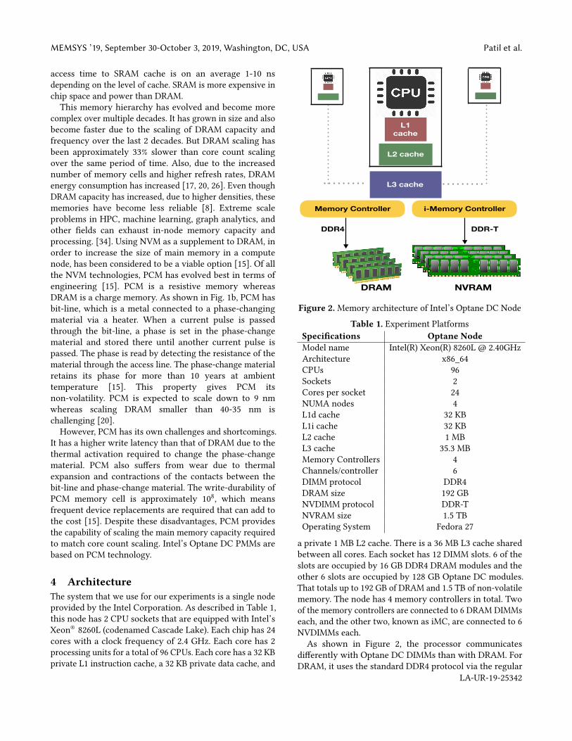
4 ArchitectureThe system that we use for our experiments is a single nodeprovided by the Intel Corporation. As described in Table 1,this node has 2 CPU sockets that are equipped with Intel’sXeon® 8260L (codenamed Cascade Lake). Each chip has 24cores with a clock frequency of 2.4 GHz. Each core has 2processing units for a total of 96 CPUs. Each core has a 32 KBprivate L1 instruction cache, a 32 KB private data cache, and
L1 cache
L2 cache
L3 cache
DRAM NVRAM
Memory Controller i-Memory Controller
DDR-TDDR4
Figure 2. Memory architecture of Intel’s Optane DC NodeTable 1. Experiment Platforms
Specifications Optane NodeModel name Intel(R) Xeon(R) 8260L @ 2.40GHzArchitecture x86_64CPUs 96Sockets 2Cores per socket 24NUMA nodes 4L1d cache 32 KBL1i cache 32 KBL2 cache 1 MBL3 cache 35.3 MBMemory Controllers 4Channels/controller 6DIMM protocol DDR4DRAM size 192 GBNVDIMM protocol DDR-TNVRAM size 1.5 TBOperating System Fedora 27
a private 1 MB L2 cache. There is a 36 MB L3 cache sharedbetween all cores. Each socket has 12 DIMM slots. 6 of theslots are occupied by 16 GB DDR4 DRAM modules and theother 6 slots are occupied by 128 GB Optane DC modules.That totals up to 192 GB of DRAM and 1.5 TB of non-volatilememory. The node has 4 memory controllers in total. Twoof the memory controllers are connected to 6 DRAM DIMMseach, and the other two, known as iMC, are connected to 6NVDIMMs each.As shown in Figure 2, the processor communicates
differently with Optane DC DIMMs than with DRAM. ForDRAM, it uses the standard DDR4 protocol via the regular
LA-UR-19-25342
Optane DC performance MEMSYS ’19, September 30-October 3, 2019, Washington, DC, USA
memory controller whereas for Optane DC it uses theDDR-T protocol via the i-memory controller (iMC). Usingthis proprietary add-on protocol to the DDR4 protocol, theOptane DC achieves asynchronous command/data timingand variable-latency memory transactions. To communicatewith the iMC, the module controller in Optane DC PMMuses a request/grant scheme. The direction and timing ofthe data bus on which Optane DC resides is controlled bythe processor. The processor sends a command packet perrequest to the Optane DC memory controller. The modulesuse 256 byte cache line access granularity which is largerthan the 64 byte cache line access granularity used inDRAM.[10]. Intel’s asynchronous DRAM refresh (ADR)guarantees the CPU stores that reach it, will survive apower failure. The stores are flushed to NVDIMMs in lessthan 100 µs, which is the hold-up time. The iMC falls in theADR domain but the caches do not. So, the stores will bepersistent only after they reach iMC for which it uses a72-bit data bus and transfers data in cache line granularityfor CPU loads and stores. Optane DC has an on-DIMMApache Pass controller that handles memory accessrequests and the processing required on NVDIMM. Theon-DIMM controller internally translates the addresses ofall access requests for wear-levelling and bad-blockmanagement. It maintains an address indirection tableon-DIMM that translates the DIMM’s physical addresses toan internal device address. The table is also backed up onDRAM. Accessing data on Optane DC occurs after thetranslation. The controller translates 64 byte load/storesinto 256 byte accesses due to the higher cache line accessgranularity of Optane DC which causes write amplification[10].The Optane DC operates in three different modes. With
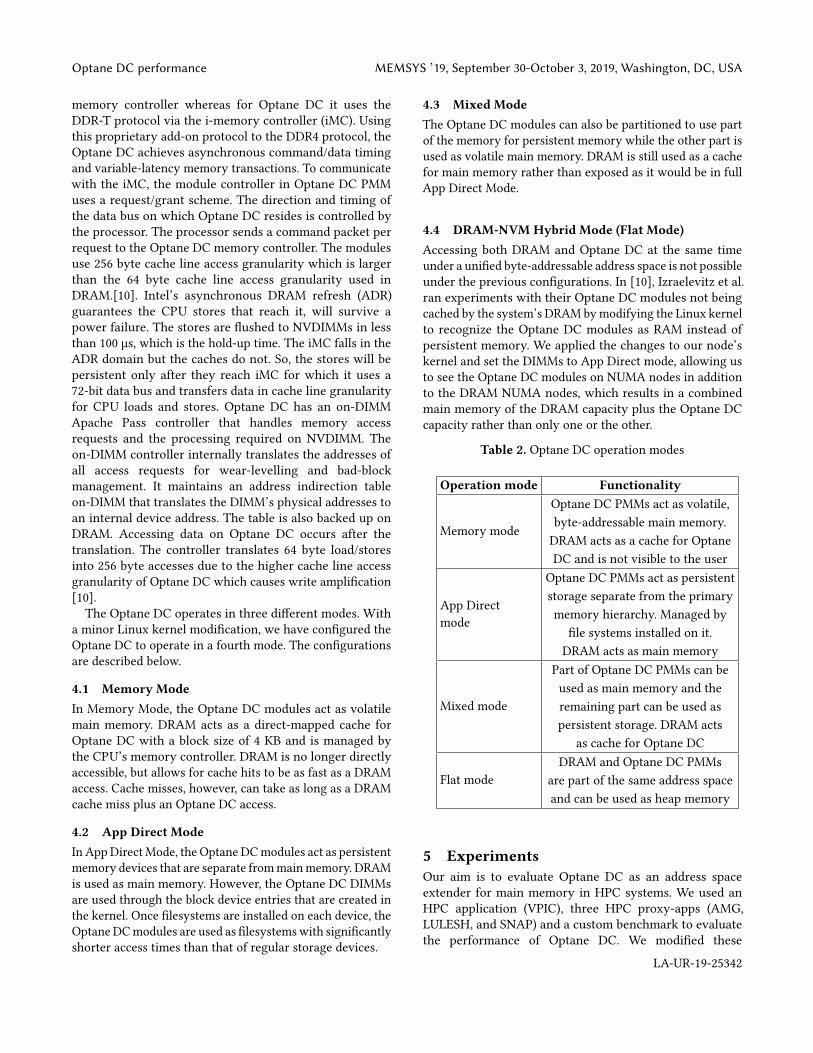
a minor Linux kernel modification, we have configured theOptane DC to operate in a fourth mode. The configurationsare described below.
4.1 Memory ModeIn Memory Mode, the Optane DC modules act as volatilemain memory. DRAM acts as a direct-mapped cache forOptane DC with a block size of 4 KB and is managed bythe CPU’s memory controller. DRAM is no longer directlyaccessible, but allows for cache hits to be as fast as a DRAMaccess. Cache misses, however, can take as long as a DRAMcache miss plus an Optane DC access.
4.2 App Direct ModeIn AppDirect Mode, the Optane DCmodules act as persistentmemory devices that are separate frommainmemory. DRAMis used as main memory. However, the Optane DC DIMMsare used through the block device entries that are created inthe kernel. Once filesystems are installed on each device, theOptane DCmodules are used as filesystemswith significantlyshorter access times than that of regular storage devices.
4.3 Mixed ModeThe Optane DC modules can also be partitioned to use partof the memory for persistent memory while the other part isused as volatile main memory. DRAM is still used as a cachefor main memory rather than exposed as it would be in fullApp Direct Mode.
4.4 DRAM-NVM Hybrid Mode (Flat Mode)Accessing both DRAM and Optane DC at the same timeunder a unified byte-addressable address space is not possibleunder the previous configurations. In [10], Izraelevitz et al.ran experiments with their Optane DC modules not beingcached by the system’s DRAM bymodifying the Linux kernelto recognize the Optane DC modules as RAM instead ofpersistent memory. We applied the changes to our node’skernel and set the DIMMs to App Direct mode, allowing usto see the Optane DC modules on NUMA nodes in additionto the DRAM NUMA nodes, which results in a combinedmain memory of the DRAM capacity plus the Optane DCcapacity rather than only one or the other.
Table 2. Optane DC operation modes
Operation mode Functionality
Memory mode
Optane DC PMMs act as volatile,byte-addressable main memory.DRAM acts as a cache for OptaneDC and is not visible to the user
App Directmode
Optane DC PMMs act as persistentstorage separate from the primarymemory hierarchy. Managed by
file systems installed on it.DRAM acts as main memory
Mixed mode
Part of Optane DC PMMs can beused as main memory and theremaining part can be used aspersistent storage. DRAM acts
as cache for Optane DC
Flat modeDRAM and Optane DC PMMs
are part of the same address spaceand can be used as heap memory
5 ExperimentsOur aim is to evaluate Optane DC as an address spaceextender for main memory in HPC systems. We used anHPC application (VPIC), three HPC proxy-apps (AMG,LULESH, and SNAP) and a custom benchmark to evaluatethe performance of Optane DC. We modified these
LA-UR-19-25342

MEMSYS ’19, September 30-October 3, 2019, Washington, DC, USA Patil et al.
applications1 so we can allocate all the data either on theDRAM, or on Optane DC. We then compared the statisticswe collected for both configurations. We performed apreliminary performance characterization using a customSTREAM-like benchmark that evaluates the performance ofdifferent types of kernels encountered in HPC applications.Memory bandwidth information was collected for everystream used in a kernel that was parallelized usingOpenMP [5]. The streams used in the benchmarks arerepresentative of most of the streams found in HPCapplications. We focus on different access patterns of datastructures like sequential, strided, and random access. Wealso collect bandwidth numbers for matrix accesses andoperations, for example, row-major access and stenciloperations. We have a test where we bypass the L3 cache byaccessing elements that are apart by number of elementsthat fit in L3 cache.Our experiments ran on the Optane DC node described
in Section 4 and Table 1. We set the Optane DC modulesin Memory Mode and the DRAM-NVM Hybrid Mode (FlatMode), and compared the performance of all the applicationsfor each mode. In Flat mode, we allocated memory on NVMand DRAM for different runs. In memory mode, memorywas only allocated on NVM as DRAM was used as cache forNVM.
We performed strong and weak scaling for all of the HPCmini-apps and measured the total execution times, memorybandwidth, power consumption, last-level cache misses anddouble-precision floating point operations per second. Weused LIKWID [32] to collect performance counters. For ourcustom benchmark, we collected only the memorybandwidth for different kernels that we test.
Keeping in mind that we had Optane DC PMMs on only asingle node, our experiments were not conducted on largenumber of processes or memory sizes. We ensured that ourproblem sizes were big enough to not fit into the last-levelcache and so we can get a fair depiction of the performanceof the different memories. Our problem sizes lie in asmall/medium range as recommended by the authors of themini-apps. We did not scale the number of processes tomore than 48, i.e., half the number of processing units toavoid oversubscribing of resources. This was done in orderto get correct performance numbers from the hardwareperformance counters. For the custom benchmark, weaveraged the bandwidth measurements over 10 runs forevery kernel which had a standard deviation up to 8%. Forthe HPC mini-apps, we average all measurements over 4runs with a standard deviation of 11% for execution time.We describe the applications we use for our experimentsbelow.1In order to have the applications allocate their data on Optane DC orDRAM only, we modified the applications to use the Simple Interface forComplex Memory (SICM) [28] library, a NUMA-aware arena allocator forheterogeneous memory.
5.1 AMGAMG is a parallel algebraic multi-grid solver for linearsystems arising from problems on unstructured grids [39]. Itwas developed at Lawrence Livermore National Laboratory(LLNL). It is an SPMD code that uses MPI and OpenMPthreading within MPI tasks. AMG is a highly synchronouscode. The communication and computation patterns exhibitthe surface-to-volume relationship common to manyparallel scientific codes. We use the default Laplace typeproblem on a cube with a 27-point stencil.
5.2 LULESHLULESH [13] is a highly simplified application, hard-codedto only solve a simple Sedov blast problem with analyticanswers. It is C++ based applications. It was developed atLLNL as a part of co-design efforts for exascalecomputations. LULESH approximates the hydrodynamicsequations discretely by partitioning the spatial problemdomain into a collection of volumetric elements defined bya mesh. It uses MPI and OpenMP for parallelization and isalso memory bound.
5.3 VPICVector Particle-In-Cell (VPIC) [2] is a simulation codedeveloped at Los Alamos National Laboratory (LANL). It isan application that models kinetic plasmas in 1 to 3dimensions. It uses MPI and OpenMP for parallelism. Thecode is comprised of kernels that compute multiple datastreams at the same time and operate on entire datastructures. The data structures scale based on the inputdecks and hence make VPIC memory bound.
5.4 SNAPSNAP [29] is based on the PARTISN code from LANL. SNAPmimics the computational workload, memory requirements,and communication patterns of PARTISN. The equation itsolves has been composed to use the same number ofoperations, uses the same data layout, and loads elements ofthe arrays in approximately the same order. SNAP uses MPIto scale for HPC. We use the SNAP-C code. It is also amemory-bound application but is more bound bybandwidth than latency.
6 Results6.1 Performance evaluation of different streams on
Optane DCWe evaluate the performance of various streams executedon Optane DC compared to DRAM. We perform strongscaling on the streams by increasing the OpenMP threadsfrom 1 to 96 for different runs. We pinned the threads usingnumactl -C to specific processing units and thenallocated the streams on every NUMA node to evaluate theeffect of NUMA distances on memory bandwidth. We
LA-UR-19-25342
Optane DC performance MEMSYS ’19, September 30-October 3, 2019, Washington, DC, USA
1
10
100
1000
10000
100000
1 8 16 24 32 40 48 56 64 72 80 88 96
Band
width
(MB/s)
OMP threads
Local DRAM BWRemote DRAM BW
Local NVM BWRemote NVM BW
(a) Write-only stream bandwidth on the Optane node
1101001000100001000001 × 106
1 8 16 24 32 40 48 56 64 72 80 88 96
Band
width
(MB/s)
OMP threads
Local DRAM BWRemote DRAM BW
Local NVM BWRemote NVM BW
(b) 1 write+4 read stream bandwidth on the Optane nodeFigure 3. Bandwidth measurement of Write-only and 1-write+4-read sequential access streams
1
10
100
1000
10000
100000
1 8 16 24 32 40 48 56 64 72 80 88 96
Band
width
(MB/s)
OMP threads
Local DRAM BWRemote DRAM BW
Local NVM BWRemote NVM BW
(a) Multiple stream kernel bandwidth on the Optane node
1101001000100001000001 × 106
1 8 16 24 32 40 48 56 64 72 80 88 96
Band
width
(MB/s)
OMP threads
Local DRAM BWRemote DRAM BW
Local NVM BWRemote NVM BW
(b) Strided stream bandwidth on the Optane nodeFigure 4. Bandwidth measurement of Multiple 1-write+4-read sequential access and Fixed stride access stream
1
10
100
1000
10000
1 8 16 24 32 40 48 56 64 72 80 88 96
Band
width
(MB/s)
OMP threads
Local DRAM BWRemote DRAM BW
Local NVM BWRemote NVM BW
(a) Random stream bandwidth on the Optane node
1
10
100
1000
10000
100000
1 8 16 24 32 40 48 56 64 72 80 88 96
Band
width
(MB/s)
OMP threads
Local DRAM BWRemote DRAM BW
Local NVM BWRemote NVM BW
(b) LLC bypass stream bandwidth on the Optane nodeFigure 5. Bandwidth measurement of Random and LLC bypass stride access stream
1101001000100001000001 × 106
1 8 16 24 32 40 48 56 64 72 80 88 96
Band
width
(MB/s)
OMP threads
Local DRAM BWRemote DRAM BW
Local NVM BWRemote NVM BW
(a) Row major matrix stream bandwidth on the Optane node
1
10
100
1000
10000
100000
1 8 16 24 32 40 48 56 64 72 80 88 96
Band
width
(MB/s)
OMP threads
Local DRAM BWRemote DRAM BW
Local NVM BWRemote NVM BW
(b) Column major matrix stream bandwidth on the Optane nodeFigure 6. Bandwidth measurement of Row-major and Column-major matrix access stream
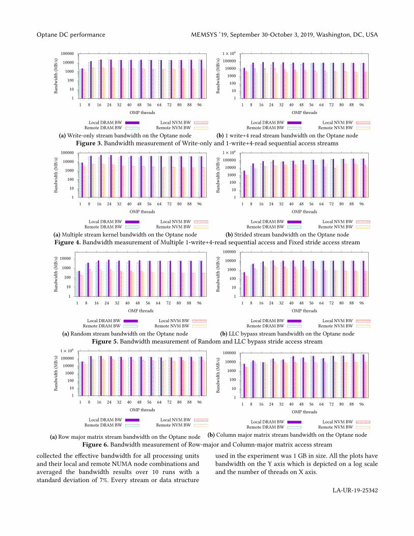
collected the effective bandwidth for all processing unitsand their local and remote NUMA node combinations andaveraged the bandwidth results over 10 runs with astandard deviation of 7%. Every stream or data structure
used in the experiment was 1 GB in size. All the plots havebandwidth on the Y axis which is depicted on a log scaleand the number of threads on X axis.
LA-UR-19-25342
MEMSYS ’19, September 30-October 3, 2019, Washington, DC, USA Patil et al.
1101001000100001000001 × 106
1 8 16 24 32 40 48 56 64 72 80 88 96
Band
width
(MB/s)
OMP threads
Local DRAM BWRemote DRAM BW
Local NVM BWRemote NVM BW
(a) Row+column major matrix stream bandwidth on Optane node
1101001000100001000001 × 1061 × 107
1 8 16 24 32 40 48 56 64 72 80 88 96
Band
width
(MB/s)
OMP threads
Local DRAM BWRemote DRAM BW
Local NVM BWRemote NVM BW
(b) 9-cell stencil stream bandwidth on the Optane nodeFigure 7. Bandwidth measurement of Row-Column matrix and 9 point stencil stream
Fig. 3a depicts results for strong scaling of the write-onlystream. The average bandwidth for local NUMA nodespeaks at 48 threads and then it plateaus. The bandwidth ofremote NUMA nodes also increases with the number ofOpenMP threads and peaks at 24 threads after which itplateaus as well. This effect is caused by oversubscribing ofresources beyond 48 threads which causes the memorycontroller queues to overflow. This can lead to serializationof loads and stores due to back pressure and nullifies thebenefit of bank parallelism. We observe that the NUMAdistances affect bandwidth of NVM up to 22% and up to 16%for DRAM in case of strong scaling for the write onlystream. Fig. 3b shows results for the kernel with a singlewrite and four read stream. The same effect is observed asfor the write-only stream but the relative bandwidth foreach run is more than 3x the bandwidth of the write-onlystream. This effect is observed for both DRAM and NVM,but DRAM achieves 8x higher bandwidth than NVM beforeoversubscribing. The difference between DRAM and NVMbandwidth worsens beyond 48 threads where they start toplateau. Such sequentially accessed streams are used mostlyduring initialization or problem generation phases of HPCapplications. The above results indicate that utilization oflocal DRAM nodes in this phase is critical while notoversubscribing to compute resources.Fig. 4a provides results for a kernel with multiple single
write plus 4 read streams. The performance is similar towhat is observed for the single write and four read streambut the effective bandwidth is slightly lower. The bandwidthfor DRAM is 30% lesser than the single write and four readstream and 50% lesser for NVM. Such streams don’t need alot of parallelism to achieve maximum bandwidth howeverthe access latency of the memory device will affect theperformance. Fig. 4b depicts results for a kernel with a fixedstride access for increasing OpenMP threads. The stride isbigger than the cache line size. For this stream the NUMAdistances have no effect on the memory bandwidth, exceptfor fewer than 24 threads for DRAM. NVM scales similarlyto the previous streams but achieves higher memorybandwidth. The memory bandwidth of DRAM keepsincreasing with the number of threads until it peaks at 48
threads for NVM. This indicates that NVM bandwidth maybe constrained by the core count irrespective of the accesspattern. This stream achieves up to 8x the bandwidth ofwrite-only stream for DRAM and 10x the bandwidth of thesame for NVM. Fig. 5a shows results from a randomlyaccessed single write plus 4 read stream, which achieves thelowest effective bandwidth of all streams. The randomaccesses are determined by an indirection array that isinitialized by the rand() function that generates the order ofindices to access. The memory bandwidth for local DRAMand NVM nodes is up to 40% higher till 48 threads afterwhich it plateaus and is unaffected by NUMA distances.This effect is observed because of not allowing the HWprefetcher to take advantage of any temporal locality.Hence, effective bandwidth is so low. Fig. 5b illustratesresults for a single write plus 4 read stream forced to bypassthe L3 cache for every access. In this stream, we observethat the bandwidth achieved by DRAM is up to 5x higherthan NVM till 48 threads. The bandwidth remains plateausfor all NUMA nodes beyond that. This result indicates thatif we take the caches out of the picture, the effectivebandwidth achieved by Optane DC is not affected as muchas DRAM despite the higher access latencies. Such streamswith varying access patterns are common in thecomputation phase of HPC applications. It becomesessential to identify the access patterns of each linearstream at every stage of the program and place the streamin the most effective memory node given the amount ofcompute resources subscribed to.
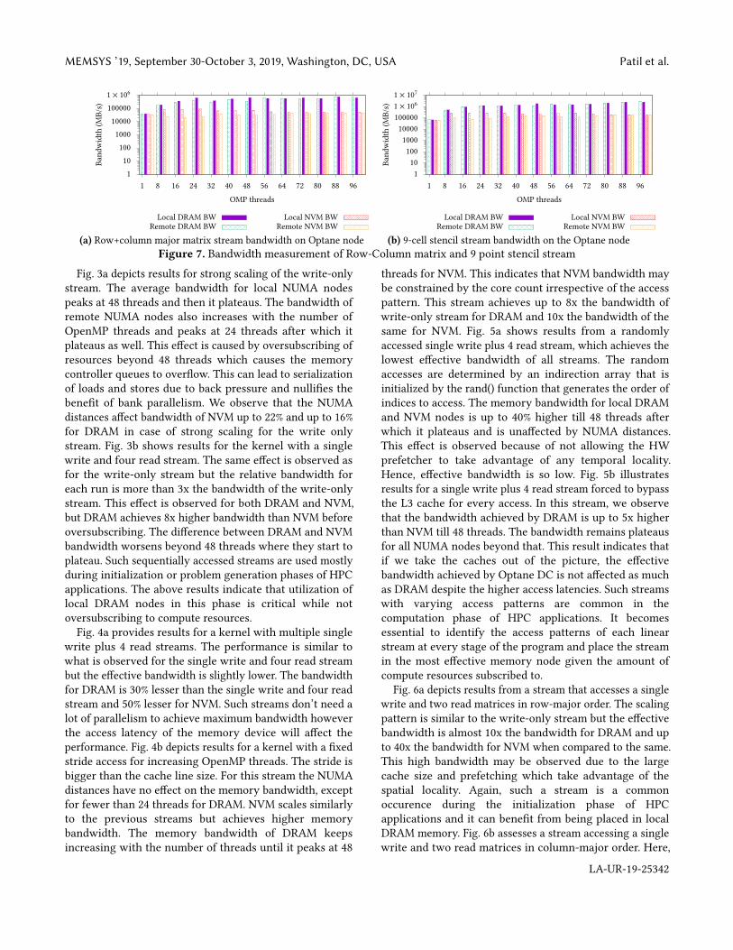
Fig. 6a depicts results from a stream that accesses a singlewrite and two read matrices in row-major order. The scalingpattern is similar to the write-only stream but the effectivebandwidth is almost 10x the bandwidth for DRAM and upto 40x the bandwidth for NVM when compared to the same.This high bandwidth may be observed due to the largecache size and prefetching which take advantage of thespatial locality. Again, such a stream is a commonoccurence during the initialization phase of HPCapplications and it can benefit from being placed in localDRAM memory. Fig. 6b assesses a stream accessing a singlewrite and two read matrices in column-major order. Here,
LA-UR-19-25342

Optane DC performance MEMSYS ’19, September 30-October 3, 2019, Washington, DC, USA
the NVM bandwidth remains steady with the increase inthreads with a slight advantage for local NVM nodes.However, for DRAM, NUMA distances do not make a bigdifference and the bandwidth keeps increasing with theincreasing number of threads. The bandwidth is 3x lowerfor DRAM and 8x lower for NVM than the row-majorstream for most threads, except for the 2 highest threadcounts, where DRAM bandwidth jumps up to 86 GB/s.Fig. 7a shows results for a kernel that accesses a single writeplus two read matrices stream, all in row-major except forthe last read stream in column-major order. It achieves 4xhigher memory bandwidth than the row major stream forboth DRAM and NVM. It achieves such high bandwidth dueto spatial locality and prefetching in the cache. The scalingpattern is similar to the row major access stream butachieves substantially higher bandwidth for both memories.Lower thread counts give advantage to local NUMA nodebut beyond 48 threads, there is no difference. Fig. 7b depictsresults for a 9-point stencil kernel, which scales similarlyFig. 7a but with approximately 40x the bandwidth for allthread counts and memories. This stream achieves thehighest bandwidth of all the streams due to a lot of spatialand temporal locality in the cache. The bandwidth observedis effectively the bandwidth of the cache. Such matrixstreams occur during the computation phase of a HPCapplication. Although NUMA distances do influence theeffective bandwidth of these streams, the memory deviceused affects the bandwidth significantly with increasingnumber of threads. Also the effective use of cache localitycan help in achieving higher performance for both memorydevices.Taking all the results into account, we can infer that the
higher latency of Optane DC and the lack of optimal cachesupport causes it to not perform as well as DRAM. Weobserve that with effective caching and prefetching, OptaneDC can deliver much better performance than what isobserved in our evaluation. However, these results give afair idea of which workloads can benefit from NVM andgives a quantification of the performance impact by usingNVM in place of DRAM.
6.2 HPC Benchmark evaluationFor benchmarks, we plot the application bandwidth andexecution time measurements together in a single graph toobserve their correlation. Similarly, we plot the energyconsumption and execution time measurements together.We also plot the cycles/instruction (CPI) and L3 miss ratiotogether. We plot these graphs for both strong and weakscaling experiments. For bandwidth and execution timegraphs, we plot execution time on the left-hand side y-axisin seconds and depicted as lines. The bandwidth is plottedon the right-hand side y-axis in megabytes/seconds (MB/s)and depicted as a bar chart. For energy consumption andexecution time graphs, we again plot our execution time on
the left-hand side y-axis as lines. The energy is plotted onthe right-hand side y-axis in Joules (J) as a bar chart. ForCPIs and L3 miss ratio graphs, we plot the CPIs on theleft-hand side y-axis as lines. The L3 miss ratio is plotted onthe right-hand side y-axis as a bar chart. Both CPIs and L3miss ratio have no unit. Bandwidth is plotted on alogarithmic scale whereas all other measurements areplotted on a linear scale. The x-axis depicts the number ofMPI processes for a given execution.
6.2.1 AMG resultsFig. 8a and Fig. 8b depict the graphs for strong and weakscaling of AMG, respectively. For strong scaling, we scalethe processes from 1 to 8 using MPI and keep the data sizeconstant by reducing the size per processor from 256 to 128.For weak scaling, we again scale the processes from 1 to 8and keep the size per processor same at 256 as we scale thedata size proportionally. We observe that memorybandwidth for Optane-only execution is 2 to 3 orders ofmagnitude lower than DRAM-only and Memory-modeexecutions. This results in more than 2x higher executiontimes for Optane-only execution. This result is observed forboth strong and weak scaling cases. The observedbandwidth remains fairly constant for both strong and weakscaling across all number of processes for DRAM-only andMemory-mode executions but rises for Optane-onlyexecution. The lower bandwidth for Optane-only executionis a result of the higher access latency of Optane DC. TheMemory-mode execution matches the performance ofDRAM-only execution because it uses DRAM as a cache.The problem sizes for this experiment are small enough tofit into DRAM. Hence, there is minimal difference betweenthe performance of DRAM-only and Memory-modeexecutions. Fig. 9a and Fig. 9b depict the energyconsumption and execution time of all three executions ofAMG for strong and weak scaling. We observe that theenergy consumption of Optane-only execution is 2x higherthan DRAM-only and Memory-mode executions. This isdue to its higher execution time even though the powerconsumed by Optane-only execution is lower than the otherexecutions. Fig. 10a and Fig. 10b depict the L3 cache missesand Cycles/Instruction(CPI) for strong and weak scaling ofAMG for all 3 executions. In strong scaling, we observe thatthe CPIs for Optane-only execution are higher for lownumber of processes. For higher number of processes theyare almost equal to the other 2 executions. However, the L3cache misses increase rapidly with the number of processes.This also explains the difference in execution times ofOptane-only execution and other 2 executions. The increasein L3 cache misses in Optane-only execution is observedunder weak scaling as well but the CPIs are consistentlyhigher than the CPIs for the other 2 executions. AMG is amemory bound application that is heavily affected bymemory access speeds. Hence, the Optane-only executions
LA-UR-19-25342

MEMSYS ’19, September 30-October 3, 2019, Washington, DC, USA Patil et al.
050100150200250300350
1 2 4 8110100100010000100000
Time(se
cond
s)
Band
width
(MB/s)
MPI Processes
DRAM Total BWDRAM Read BWDRAMWrite BW
Optane Total BWOptane Read BWOptane Write BW
Memory-mode Total BWMemory-mode Read BWMemory-mode Write BW
DRAM Solve timeOptane Solve time
Memory-mode Solve time
(a) AMG Bandwidth Strong Scaling
0100200300400500
1 2 4 8110100100010000100000
Time(se
cond
s)
Band
width
(MB/s)
MPI Processes
DRAM Total BWDRAM Read BWDRAMWrite BW
Optane Total BWOptane Read BWOptane Write BW
Memory-mode Total BWMemory-mode Read BWMemory-mode Write BW
DRAM Solve timeOptane Solve time
Memory-mode Solve time
(b) AMG Bandwidth Weak ScalingFigure 8. Bandwidth measurement for AMG
050100150200250300350
1 2 4 80200040006000800010000
Time(se
cond
s)
Energy
(J)
MPI Processes
DRAM EnergyOptane Energy
Memory-mode Energy
DRAM Solve timeOptane Solve time
Memory-mode Solve time
(a) AMG Memory Energy Consumption Strong Scaling
0100200300400500
1 2 4 802000400060008000100001200014000
Time(se
cond
s)
Energy
(J)
MPI Processes
DRAM EnergyOptane Energy
Memory-mode Energy
DRAM Solve timeOptane Solve time
Memory-mode Solve time
(b) AMG Memory Energy Consumption Weak ScalingFigure 9. Memory energy consumption for AMG
051015202530
1 2 4 800.511.522.53
Cycles/in
struction
L3Miss
ratio
MPI Processes
DRAM L3 missesOptane L3 misses
Memory-mode L3 misses
DRAM CPIOptane CPI
Memory-mode CPI
(a) AMG L3 Miss Ratio and CPI Strong Scaling
051015202530
1 2 4 800.511.522.533.5
Cycles/in
struction
L3Miss
ratio
MPI Processes
DRAM L3 missesOptane L3 misses
Memory-mode L3 misses
DRAM CPIOptane CPI
Memory-mode CPI
(b) AMG L3 Miss Ratio and CPI Weak ScalingFigure 10. L3 miss ratio and CPI for AMG
suffer from heavy performance degradation in terms ofexecution time and energy consumption. Such applicationsthat require faster access speeds will suffer from aNVM-only approach.
6.2.2 LULESH resultsFig. 11a and Fig. 11b depict the graphs for strong and weakscaling of LULESH, respectively. We increase the number ofprocessors from 1 to 27 using MPI, as LULESH accepts onlycubes of natural numbers as a valid configuration. For
LA-UR-19-25342

Optane DC performance MEMSYS ’19, September 30-October 3, 2019, Washington, DC, USA
0100200300400500
1 8 271
10
100
1000
10000
Time(se
cond
s)
Band
width
(MB/s)
MPI Processes
DRAM Total BWDRAM Read BWDRAMWrite BW
Optane Total BWOptane Read BWOptane Write BW
Memory-mode Total BWMemory-mode Read BWMemory-mode Write BW
DRAM Solve timeOptane Solve time
Memory-mode Solve time
(a) LULESH Bandwidth Strong Scaling
0100200300400500
1 8 271
10
100
1000
10000
Time(se
cond
s)
Band
width
(MB/s)
MPI Processes
DRAM Total BWDRAM Read BWDRAMWrite BW
Optane Total BWOptane Read BWOptane Write BW
Memory-mode Total BWMemory-mode Read BWMemory-mode Write BW
DRAM Solve timeOptane Solve time
Memory-mode Solve time
(b) LULESH Bandwidth Weak ScalingFigure 11. Bandwidth measurement for LULESH
050100150200250300
1 8 27010002000300040005000600070008000
Time(se
cond
s)
Energy
(J)
MPI Processes
DRAM EnergyOptane Energy
Memory-mode Energy
DRAM Solve timeOptane Solve time
Memory-mode Solve time
(a) LULESH Memory Energy Consumption Strong Scaling
0100200300400500
1 8 2702000400060008000100001200014000
Time(se
cond
s)
Energy
(J)
MPI Processes
DRAM EnergyOptane Energy
Memory-mode Energy
DRAM Solve timeOptane Solve time
Memory-mode Solve time
(b) LULESH Memory Energy Consumption Weak ScalingFigure 12.Memory energy consumption for LULESH
05101520253035
1 8 2700.511.522.5
Cycles/in
struction
L3Miss
Ratio
MPI Processes
DRAM L3 missesOptane L3 misses
Memory-mode L3 misses
DRAM CPIOptane CPI
Memory-mode CPI
(a) LULESH L3 Miss Ratio and CPI Strong Scaling
0102030405060
1 8 2700.511.522.533.5
Cycles/in
struction
L3Miss
ratio
MPI Processes
DRAM L3 missesOptane L3 misses
Memory-mode L3 misses
DRAM CPIOptane CPI
Memory-mode CPI
(b) LULESH L3 Miss Ratio and CPI Weak ScalingFigure 13. L3 miss ratio and CPI for LULESH
strong scaling, we keep the problem size constant at 125000data points and increase the number of processors. Weobserve that when LULESH is running only on Optane DCin flat mode, it has a 50% higher execution time thanDRAM-only and Memory-mode configurations for a single
process and 8 processes. For 27 processes, the executiontime is approximately 6x higher. This effect is observedbecause the memory bandwidth is almost an order ofmagnitude lower than DRAM-only and Memory-modeexecutions. The difference in execution time is more
LA-UR-19-25342

MEMSYS ’19, September 30-October 3, 2019, Washington, DC, USA Patil et al.
amplified in weak scaling for 27 processes due to lowerbandwidth. In weak scaling, we keep the number of datapoints per process constant at 15,625. The low bandwidthon Optane-only execution is due to the high access latencyof Optane DC. We do not observe this effect inMemory-mode because of the DRAM caching inMemory-mode. Hence, there is no difference in executiontime for DRAM-only and Memory-mode execution as theaccess latency would be the same. In flat mode, Intel’s ADRis at work to guarantee persistence of data, which can behampering performance and the write amplification mightincrease access latencies, too. The memory bandwidth inweak scaling is similar to strong scaling except for singleprocess execution in strong scaling, where Optane DC has 2orders of magnitude lower bandwidth. Fig. 12a and 12bdepict the memory energy consumption of LULESH in eachmode for strong and weak scaling, respectively. We observethat the energy consumption for Optane DC is up to 60%higher than DRAM-only and Memory-mode executions.This is in direct correlation to the execution time becausethe power consumption for Optane DC is up to 30% lessthan DRAM. For smaller problem sizes under weak scalingwith fewer threads the energy consumption of Optane DCis similar to the other executions. A trade-off betweencapacity, problem size and performance needs to beachieved to keep the application execution within desiredenergy budgets. Fig. 13a and Fig. 13b depict the L3 cachemiss ratio and CPIs for LULESH strong and weak scaling,respectively. For strong scaling, the L3 cache missesincrease with the number of processes but they are lowerfor Optane-only execution on 27 nodes. In weak scaling, theCPIs are 3x higher compared to DRAM-only and the L3cache misses are significantly higher. These add to theexecution time, explaining the difference in execution timefor weak scaling of LULESH. Applications like LULESH aredependent on memory bandwidth for performance. Theseapplications can reduce their energy consumption withNVM when they are running smaller problem sizes andfewer threads.
6.2.3 VPIC resultsFig. 14a and Fig. 14b depict the execution time and memorybandwidth for strong and weak scaling of VPIC. We use the’lpi’ input deck provided by the authors of the benchmarkfor our experiments. For strong scaling, we increase thenumber of processes from 1 to 8 using MPI and keep theproblem size the same by changing the ’nppc’ value from2048 to 256. The ’nppc’ variable in the input deckdetermines the number of particles/cell for each species inthe plasma. We observe that NVM-only execution of VPICis 2 to 16% slower than DRAM-only and Memory-modeexecutions. For weak scaling, we keep the problem size perprocess same by keeping the ’nppc’ value at 512. Thisslowdown is caused by the lower bandwidth observed for
Optane-only execution. Optane-only memory bandwidth isat least an order of magnitude lower than DRAM-only andMemory-mode bandwidth for larger number of processes incase of strong scaling. For weak-scaling, the memorybandwidth of Optane-only execution is similar toDRAM-only execution and Memory-mode execution andhence there is no difference in execution times either.Fig. 15a and Fig. 15b depict that the memory energyconsumption for VPIC strong and weak scaling,respectively. The Optane-only execution’s energyconsumption remains constant with strong scaling of VPICsimilar to the DRAM energy consumption. However underweak scaling, Optane-only execution’s energy consumptionrises at slower rate than the other 2 executions. As theexecution times are similar for all execution under weakscaling, the energy consumed by all three executions is alsosimilar. Fig. 16a and Fig. 16b depict the L3 cache miss ratioand CPIs for strong scaling and weak scaling of VPIC. Eventhough the cache misses increase with strong scaling forOptane DC execution, the CPIs remain lower thanDRAM-only execution. The cache miss ratio forMemory-mode execution rises at a slower rate thanNVM-only and DRAM-only execution. In weak scaling,Optane-only execution results in fewer L3 cache missesthan DRAM-only and Memory-mode execution but higherCPIs. This keeps the execution times of Optane-onlyexecution low for weak scaling. VPIC optimizes its cachehits, as seen in the results, to achieve higher performanceand hence there is minimal difference in execution times ofall three executions even though there is a significantdifference in bandwidth. Such applications can benefit fromOptane DC by reducing energy consumption while notcompromising on performance.
6.2.4 SNAP resultsFig. 17a and Fig. 17b depict the memory bandwidth andexecution time for strong and weak scaling of SNAP inOptane-only, DRAM-only, and Memory-mode executions.We use MPI to scale the number of processes from 1 to 8.We use the C-version of SNAP that is compiled with mpicc.Here, we observe that the execution times in strong scalingvary only slightly for all the three executions. Optane DCmemory bandwidth increases with increasing number ofprocesses and is the highest out of all three executions for 8processes. This is reflected in the execution times of all 3executions. However, for weak scaling the execution timeincreases for Optane-only execution when we scale up to 8processes. We also observe that the memory bandwidth forOptane-only execution does not increase with weak scaling.This explains the 2x higher execution time for Optane-onlyexecution compared to DRAM-only and Memory-modeexecution. Fig. 18a and Fig. 18b depict the energyconsumption of SNAP execution in Optane-only,DRAM-only, and Memory-mode executions. The energy
LA-UR-19-25342

Optane DC performance MEMSYS ’19, September 30-October 3, 2019, Washington, DC, USA
010002000300040005000
1 2 4 81
10
100
1000
10000
Time(se
cond
s)
Band
width
(MB/s)
MPI Processes
DRAM Total BWDRAM Read BWDRAMWrite BW
Optane Total BWOptane Read BWOptane Write BW
Memory-mode Total BWMemory-mode Read BWMemory-mode Write BW
DRAM Solve timeOptane Solve time
Memory-mode Solve time
(a) VPIC Bandwidth Strong Scaling
020406080100120140
1 2 4 81
10
100
1000
10000
Time(se
cond
s)
Band
width
(MB/s)
MPI Processes
DRAM Total BWDRAM Read BWDRAMWrite BW
Optane Total BWOptane Read BWOptane Write BW
Memory-mode Total BWMemory-mode Read BWMemory-mode Write BW
DRAM Solve timeOptane Solve time
Memory-mode Solve time
(b) VPIC Bandwidth Weak ScalingFigure 14. Bandwidth measurement for VPIC
010002000300040005000
1 2 4 8020000400006000080000100000120000
Time(se
cond
s)
Energy
(J)
MPI Processes
DRAM EnergyOptane Energy
Memory-mode Energy
DRAM Solve timeOptane Solve time
Memory-mode Solve time
(a) VPIC Memory Energy Consumption Strong Scaling
020406080100120140
1 2 4 805001000150020002500300035004000
Time(se
cond
s)
Energy
(J)
MPI Processes
DRAM EnergyOptane Energy
Memory-mode Energy
DRAM Solve timeOptane Solve time
Memory-mode Solve time
(b) VPIC Memory Energy Consumption Weak ScalingFigure 15.Memory energy consumption for VPIC
0510152025303540
1 2 4 80
0.5
1
1.5
2
Cycles/in
struction
L3Miss
ratio
MPI Processes
DRAM L3 missesOptane L3 misses
Memory-mode L3 misses
DRAM CPIOptane CPI
Memory-mode CPI
(a) VPIC L3 Miss Ratio and CPI Strong Scaling
0510152025303540
1 2 4 80
0.5
1
1.5
2
Cycles/in
struction
L3Miss
ratio
MPI Processes
DRAM L3 missesOptane L3 misses
Memory-mode L3 misses
DRAM CPIOptane CPI
Memory-mode CPI
(b) VPIC L3 Miss Ratio and CPI Weak ScalingFigure 16. L3 miss ratio and CPI for VPIC
consumption remain fairly constant across all threeexecutions for both strong and weak scaling. As theexecution times are similar for these executions the energyconsumption of Optane-only execution is the least amongstthe 3 executions, when the number of processes are 4.
Under weak scaling, Memory-mode consumes the leastpower overall but due to larger execution times it consumesthe maximum energy. Fig. 19a and Fig. 19b depict the plot ofL3 cache miss ratios and CPIs for strong and weak scalingof SNAP. We observe that CPIs differ significantly for
LA-UR-19-25342

MEMSYS ’19, September 30-October 3, 2019, Washington, DC, USA Patil et al.
00.51
1.52
2.53
1 2 4 8050100150200250300350
Time(se
cond
s)
Band
width
(MB/s)
MPI Processes
DRAM Total BWDRAM Read BWDRAMWrite BW
Optane Total BWOptane Read BWOptane Write BW
Memory-mode Total BWMemory-mode Read BWMemory-mode Write BW
DRAM Solve timeOptane Solve time
Memory-mode Solve time
(a) SNAP Bandwidth Strong Scaling
012345678
1 2 4 80100200300400500600700800900
Time(se
cond
s)
Band
width
(MB/s)
MPI Processes
DRAM Total BWDRAM Read BWDRAMWrite BW
Optane Total BWOptane Read BWOptane Write BW
Memory-mode Total BWMemory-mode Read BWMemory-mode Write BW
DRAM Solve timeOptane Solve time
Memory-mode Solve time
(b) SNAP Bandwidth Weak ScalingFigure 17. Bandwidth measurement for SNAP
00.51
1.52
2.53
1 2 4 80102030405060
Time(se
cond
s)
Energy
(J)
MPI Processes
DRAM EnergyOptane Energy
Memory-mode Energy
DRAM Solve timeOptane Solve time
Memory-mode Solve time
(a) SNAP Memory Energy Consumption Strong Scaling
012345678
1 2 4 8020406080100120140
Time(se
cond
s)
Energy
(J)
MPI Processes
DRAM EnergyOptane Energy
Memory-mode Energy
DRAM Solve timeOptane Solve time
Memory-mode Solve time
(b) SNAP Memory Energy Consumption Weak ScalingFigure 18.Memory energy consumption for SNAP
05101520253035
1 2 4 80
0.5
1
1.5
2
Cycles/in
struction
L3Miss
ratio
MPI Processes
DRAM L3 missesOptane L3 misses
Memory-mode L3 misses
DRAM CPIOptane CPI
Memory-mode CPI
(a) SNAP L3 Miss Ratio and CPI Strong Scaling
05101520253035
1 2 4 800.511.522.53
Cycles/in
struction
L3Miss
ratio
MPI Processes
DRAM L3 missesOptane L3 misses
Memory-mode L3 misses
DRAM CPIOptane CPI
Memory-mode CPI
(b) SNAP L3 Miss Ratio and CPI Weak ScalingFigure 19. L3 miss ratio and CPI for SNAP
strong scaling at higher number of processes, whereOptane-only execution experiences the least CPIs. The L3cache misses actually rise with increasing number ofprocessors for all three executions. The L3 cache missesscale with increasing number of processes for weak scaling,
too. However, the changes in CPIs for higher numberprocesses are erratic. The C-version of SNAP was created totake advantage of the vector operations in the Intelmicroarchitecture and is highly optimized to take advantageof the cache hierarchy and prefetching methods. Due to this,
LA-UR-19-25342

Optane DC performance MEMSYS ’19, September 30-October 3, 2019, Washington, DC, USA
the performance degradation is minimal with SNAP, whichresults in reduction in energy consumption on the lowpower Optane DC memory.
7 Future WorkIntel’s Optane DC PMM opens up a range of possibilities foruse of NVM in various applications. We plan to explore theuse of NVDIMMs in optimizing HPC applications. Thedifferent modes in which you can operate Optane DCPMMs have potential to optimize many HPC applications.With our performance characterizations, we plan to developallocation policies for NVM for different configurations.This will help accommodate large problems with fewercompute nodes and operate under a required compute andenergy budget. There are many variable components toOptane DC that need to be characterized as well to take fulladvantage of the technology, for example, its variablelatency and power consumption. We plan to study thelongevity and varying latencies of NVDIMMs when usedwith HPC workloads and their susceptibility to faults andfailures. This will help improve the resiliency of thesupercomputers that would use NVDIMMs.In addition to the massive memory capacity, NVDIMMs
have data persistence, which can help develop novelresiliency techniques. They can be used to store lightweightcheckpoints and restart processes that fail. We plan toexplore the possibility of building a fast and lightweightcheckpoint/restart mechanism for exascale supercomputers[22]. It can also be used to maintain metadata of large-scalesystems and help in lookup operations. The data stored onNVDIMMs can be used to detect and correct soft errors byusing checksums for increasing reliability. We will explorethe use of NVDIMMs to increase the reliability ofcomputations. We also plan to investigate the kernel anduser-level support required for efficient use of NVDIMMs.Compiler-based analysis and profiling information can helpoptimize the use NVDIMMs for various applications. Wewill also assess support for other memory technologies thatcan be incorporated into the DRAM-NVM hybrid memoryhierarchy.
8 ConclusionIn this paper, we performed characterization of a hybridmemory system comprising of a slower NVM device and afaster DRAM device. We conclude that using a slowerbyte-addressable memory device hampers the performanceof memory-bound HPC applications due to higher accesslatencies and lower memory bandwidth. However, using theDRAM as a cache for the slower NVM device maintains theperformance of HPC applications observed on DRAM-onlymemory systems while increasing the memory capacity ofthe system, which needs to be further verified on largeproblem sizes. Although using NVM as main memory
directly hampers the performance, it has the potential toreduce the energy consumption of HPC applications withreasonable trade-offs. Optane DC PMMs enables us to closethe gap between core count and memory capacity scaling.
AcknowledgmentsThis material is based upon work supported by UnitedStates Department of Energy National Nuclear SecurityAdministration prime contract #89233218CNA000001subcontract #508854 dated November 1, 2018 for LosAlamos National Laboratory, NSF grants 1217748 and1525609 and by the Exascale Computing Project(17-SC-20-SC), a collaborative effort of the U.S. Departmentof Energy Office of Science and the National NuclearSecurity Administration.
References[1] Dmytro Apalkov, Alexey Khvalkovskiy, StevenWatts, Vladimir Nikitin,
Xueti Tang, Daniel Lottis, Kiseok Moon, Xiao Luo, Eugene Chen,Adrian Ong, Alexander Driskill-Smith, and Mohamad Krounbi. 2013.Spin-transfer Torque Magnetic Random Access Memory (STT-MRAM).J. Emerg. Technol. Comput. Syst. 9, 2, Article 13 (May 2013), 35 pages.https://doi.org/10.1145/2463585.2463589
[2] K J Bowers, B J Albright, L Yin,WDaughton, V Roytershteyn, B Bergen,and T J T Kwan. 2009. Advances in petascale kinetic plasma simulationwith VPIC and Roadrunner. Journal of Physics: Conference Series 180(jul 2009), 012055. https://doi.org/10.1088/1742-6596/180/1/012055
[3] Dhruva R Chakrabarti, Hans-J Boehm, and Kumud Bhandari. 2014.Atlas: Leveraging locks for non-volatile memory consistency. In ACMSIGPLAN Notices, Vol. 49. ACM, 433–452.
[4] Joel Coburn, Adrian M Caulfield, Ameen Akel, Laura M Grupp,Rajesh K Gupta, Ranjit Jhala, and Steven Swanson. 2012. NV-Heaps:making persistent objects fast and safe with next-generation, non-volatile memories. ACM Sigplan Notices 47, 4 (2012), 105–118.
[5] Leonardo Dagum and Ramesh Menon. 1998. OpenMP: An Industry-Standard API for Shared-Memory Programming. IEEE Comput. Sci.Eng. 5, 1 (Jan. 1998), 46–55. https://doi.org/10.1109/99.660313
[6] Subramanya R Dulloor, Sanjay Kumar, Anil Keshavamurthy, PhilipLantz, Dheeraj Reddy, Rajesh Sankaran, and Jeff Jackson. 2014. Systemsoftware for persistent memory. In Proceedings of the Ninth EuropeanConference on Computer Systems. ACM, 15.
[7] Gurbinder Gill, Roshan Dathathri, Loc Hoang, Ramesh Peri, andKeshav Pingali. 2019. Single Machine Graph Analytics on MassiveDatasets Using Intel Optane DC Persistent Memory. CoRRabs/1904.07162 (2019). arXiv:1904.07162 http://arxiv.org/abs/1904.07162
[8] Saurabh Gupta, Tirthak Patel, Christian Engelmann, and DeveshTiwari. 2017. Failures in large scale systems: long-term measurement,analysis, and implications. In Proceedings of the InternationalConference for High Performance Computing, Networking, Storage andAnalysis. ACM, 44.
[9] Hideto Hidaka, Yoshio Matsuda, Mikio Asakura, and KazuyasuFujishima. 1990. The cache DRAM architecture: A DRAM with anon-chip cache memory. IEEE Micro 10, 2 (1990), 14–25.
[10] Joseph Izraelevitz, Jian Yang, Lu Zhang, Juno Kim, Xiao Liu,Amirsaman Memaripour, Yun Joon Soh, Zixuan Wang, Yi Xu,Subramanya R. Dulloor, Jishen Zhao, and Steven Swanson. 2019.Basic Performance Measurements of the Intel Optane DC PersistentMemory Module. CoRR abs/1903.05714 (2019). arXiv:1903.05714http://arxiv.org/abs/1903.05714
LA-UR-19-25342

MEMSYS ’19, September 30-October 3, 2019, Washington, DC, USA Patil et al.
[11] JEDEC (2017). JEDEC DDR4 SDRAM standards. https://www.jedec.org/standards-documents/docs/jesd79-4a
[12] Sudarsun Kannan, Ada Gavrilovska, Karsten Schwan, and DejanMilojicic. 2013. Optimizing checkpoints using nvm as virtual memory.In 2013 IEEE 27th International Symposium on Parallel and DistributedProcessing. IEEE, 29–40.
[13] Ian Karlin, Jeff Keasler, and Rob Neely. 2013. LULESH 2.0 Updates andChanges. Technical Report LLNL-TR-641973. 1–9 pages.
[14] Rob Latham, N Miller, Robert Ross, P Carns, and Clemson Univ. 2004.A next-generation parallel file system for Linux cluster. LinuxWorldMag. 2 (01 2004).
[15] Benjamin C Lee, Engin Ipek, Onur Mutlu, and Doug Burger. 2009.Architecting phase change memory as a scalable dram alternative.ACM SIGARCH Computer Architecture News 37, 3 (2009), 2–13.
[16] Xu Li, Kai Lu, Xiaoping Wang, and Xu Zhou. 2012. NV-process: a fault-tolerance process model based on non-volatile memory. In Proceedingsof the Asia-Pacific Workshop on Systems. ACM, 1.
[17] Kevin Lim, Jichuan Chang, Trevor Mudge, Parthasarathy Ranganathan,Steven K Reinhardt, and Thomas F Wenisch. 2009. Disaggregatedmemory for expansion and sharing in blade servers. In ACM SIGARCHcomputer architecture news, Vol. 37. ACM, 267–278.
[18] John D. McCalpin. 1991-2007. STREAM: Sustainable MemoryBandwidth in High Performance Computers. Technical Report.University of Virginia, Charlottesville, Virginia. http://www.cs.virginia.edu/stream/ A continually updated technical report.http://www.cs.virginia.edu/stream/.
[19] John D. McCalpin. 1995. Memory Bandwidth and Machine Balancein Current High Performance Computers. IEEE Computer SocietyTechnical Committee on Computer Architecture (TCCA) Newsletter (Dec.1995), 19–25.
[20] OnurMutlu. 2013. Memory scaling: A systems architecture perspective.In 2013 5th IEEE International Memory Workshop. IEEE, 21–25.
[21] Ravi Nair. 2015. Evolution of memory architecture. Proc. IEEE 103, 8(2015), 1331–1345.
[22] Onkar Patil, Saurabh Hukerikar, Frank Mueller, and ChristianEngelmann. 2017. Exploring use-cases for non-volatile memoriesin support of hpc resilience. SC Poster Session (2017).
[23] Onkar Patil, Charles Johnson, Mesut Kuscu, Joseph Tucek, Tuan Tran,and Harumi Kuno. 2009. Persistent Regions that Survive NVM MediaFailure. (2009).
[24] Georgios Psaropoulos, Ismail Oukid, Thomas Legler, Norman May,and Anastasia Ailamaki. 2019. Bridging the latency gap between NVMand DRAM for latency-bound operations. In Proceedings of the 15thInternational Workshop on Data Management on New Hardware. ACM.
[25] Simone Raoux, Feng Xiong, MatthiasWuttig, and Eric Pop. 2014. Phasechange materials and phase change memory. MRS Bulletin 39, 8 (2014),703âĂŞ710. https://doi.org/10.1557/mrs.2014.139
[26] Brian M Rogers, Anil Krishna, Gordon B Bell, Ken Vu, Xiaowei Jiang,and Yan Solihin. 2009. Scaling the bandwidth wall: challenges in andavenues for CMP scaling. ACM SIGARCH Computer Architecture News37, 3 (2009), 371–382.
[27] Thomas Shull, Jian Huang, and Josep Torrellas. 2019. Designing aUser-Friendly Java NVM Framework. (2019).
[28] SICM 2018. Proceedings of the Workshop on Memory Centric HighPerformance Computing, MCHPC@SC 2018, Dallas, TX, USA, November11, 2018. ACM. http://dl.acm.org/citation.cfm?id=3286475
[29] SNAP [n. d.]. SNAP: SN (Discrete Ordinates) Application Proxy. https://github.com/lanl/SNAP
[30] Titan (2019). TITAN. https://www.olcf.ornl.gov/olcf-resources/compute-systems/titan/
[31] TOP500 List - November 2018 (2018). TOP500 List - November 2018.https://www.top500.org/list/2018/11/
[32] Jan Treibig, Georg Hager, and Gerhard Wellein. 2010. Likwid:A lightweight performance-oriented tool suite for x86 multicore
environments. In 2010 39th International Conference on ParallelProcessing Workshops. IEEE, 207–216.
[33] Alexander van Renen, Lukas Vogel, Viktor Leis, Thomas Neumann,and Alfons Kemper. 2019. Persistent Memory I/O Primitives. arXivpreprint arXiv:1904.01614 (2019).
[34] Jeffrey S Vetter and Sparsh Mittal. 2015. Opportunities for nonvolatilememory systems in extreme-scale high-performance computing.Computing in Science & Engineering 17, 2 (2015), 73–82.
[35] Haris Volos, Andres Jaan Tack, and Michael M Swift. 2011.Mnemosyne: Lightweight persistent memory. In ACM SIGARCHComputer Architecture News, Vol. 39. ACM, 91–104.
[36] Chao Wang, Sudharshan S Vazhkudai, Xiaosong Ma, Fei Meng,Youngjae Kim, and Christian Engelmann. 2012. NVMalloc: Exposing anaggregate SSD store as a memory partition in extreme-scale machines.In 2012 IEEE 26th International Parallel and Distributed ProcessingSymposium. IEEE, 957–968.
[37] KaiWu, Frank Ober, Shari Hamlin, and Dong Li. 2017. Early Evaluationof Intel Optane Non-Volatile Memory with HPC I/O Workloads. CoRRabs/1708.02199 (2017). arXiv:1708.02199 http://arxiv.org/abs/1708.02199
[38] Jun Yang, Qingsong Wei, Cheng Chen, Chundong Wang, Khai LeongYong, and Bingsheng He. 2015. NV-Tree: reducing consistency costfor NVM-based single level systems. In 13th {USENIX} Conference onFile and Storage Technologies ({FAST} 15). 167–181.
[39] Ulrike Meier Yang et al. 2002. BoomerAMG: a parallel algebraicmultigrid solver and preconditioner. Applied Numerical Mathematics41, 1 (2002), 155–177.
LA-UR-19-25342