PEPR-III
32
1 A REPORT FOR PEPR-III Submitted by AKASH PARMAR (100170124041) In fulfillment for the award of the degree Of BACHELOR OF ENGINEERING In POWER ELECTRONICS VISHWAKARMA GOVERNMENT ENGINEERING COLLEGE, CHANDKHEDA, AHMEDABAD-382424 Gujarat Technological University, Ahmedabad. November, 2013 VISHWAKARMA GOVERNMENT ENGINEERING COLLEGE Power Electronics Department
description
Power Electronics Presentation
Transcript of PEPR-III

1
A REPORT FOR PEPR-III
Submitted by
AKASH PARMAR (100170124041)
In fulfillment for the award of the degree
Of
BACHELOR OF ENGINEERING
In
POWER ELECTRONICS
VISHWAKARMA GOVERNMENT ENGINEERING COLLEGE, CHANDKHEDA, AHMEDABAD-382424
Gujarat Technological University, Ahmedabad.
November, 2013
VISHWAKARMA GOVERNMENT ENGINEERING COLLEGE Power Electronics Department

2
CERTIFICATE DATE: 30/10/2013
This is to certify that the dissertation entitled “A REPORT FOR PROJECT-I”
has been carried out by AKASH PARMAR under my guidance in fulfilment of
the degree of Bachelor of Engineering in Power Electronics (7th Semester) of
Gujarat Technological University, Ahmedabad during the academic year,
2013-14.
Guide: Assi. Prof. Nirav D. Mehta Head of the Department Power Electronics Department. VGEC, Chandkheda. VGEC, Chandkheda.

3
ACKNOWLEDGEMENT
We heartily thank the Gujarat Technological University, whose course curriculum
provided us with an opportunity for an exposure to the application of Electronics in real life.
We express our deep gratitude to our faculty guide, Prof. Nirav D. Mehta throughout our
Project-I laboratory work constant support and guidance.
We are sincerely thankful to our respected H.O.D. Prof. K. B. Rathod, who has always
co-operated and supported us in all respect throughout our work. We are also thankful to our Prof.
H. S. Wani and Prof. A. P. Patel and other staff members of Power Electronics Department of
VGEC, Chandkheda for their co-operation and support.
We hope that this report shall be an indicator of our hard work and dedication to the task
that will lead us to the completion of the B.E in Power Electronics degree.
In the end, we are also thankful to our parents and friends for the constant support and help
generously bestowed upon us.”
- Akash Parmar (100170124041)

4
TABLE OF CONTENTS
CHAPTER NO.
TITLE PAGE NO.
1 SIMULATION WORK 6
1.1.Simulation of single phase cascade three-level h- bridge inverter using multiple pulse width modulation
7
1.1.1. Circuit diagram 7
1.1.2. Waveform 8
1.1.3. Fast Fourier Transform (FFT) analysis 11
1.1.4. Conclusion 12
1.2 Simulation of single phase cascade three-level h-bridge inverter using sinusoidal pulse width modulation
12
1.2.1. Circuit diagram 13
1.2.2. Waveform 14
1.2.3. Fast Fourier Transform (FFT) analysis 16
1.2.4. Conclusion 17
2 DATASHEET STUDY 18
2.1 Switch : power MOSFET FDD8447L 19
2.1.1. Rating 19
2.1.2. Features 19
2.1.3. Symbol and packaging 19
2.1.4. Characteristics 19
2.1.5. Application 21
2.1.6. Conclusion 21
2.2 Power MOSFET DRIVER : IR2110 22
2.2.1. Pin diagram 22
2.2.2. Discription of pin diagram 22
2.2.3. Features 23

5
2.2.4. Typical characteristics 24
2.2.5. Application 26
2.3 Controller IC : SG3524 26
2.3.1. Pin diagram 26
2.3.2. Pin discription 26
2.3.3. Features 27
2.3.4. Characteristics 28
2.3.5. Application 29
3 PCB DESIGNING OF BUCK CONVERTER 30
3.1 Top layer 31
3.2 Bottom layer 31
3.3 Silk screen 32
3.4 Copper pour layer 32

6
CHAPTER-1 SIMULATION WORK
Simulation of single phase cascade three-level h-bridge inverter using single pulse width modulation
Simulation of single phase cascade three-level h-bridge inverter using in-phase disposition pulse width modulation

7
1.1. SIMULATION OF SINGLE PHASE CASCADE THREE-LEVEL H-BRIDGE INVERTER USING SINGLE PULSE WIDTH MODULATION
1.1.1. CIRCUIT DIAGRAM

8
1.1.2. WAVEFORMS
OUTPUT OF INVERTER-1

9
OUTPUT OF INVERTER-2

10
OUTPUT OF CASCADED INVERTER

11
1.1.3. FAST FOURIER TRANSFORM (FFT) ANALYSIS
BAR CHART REPRESENTATION
LIST CHART REPRESENTATION

12
1.1.4. CONCLUSION
From the above simulation we can conclude that single phase cascade three-level H-bridge inverter with single pulse width modulation has 21.66% Total Harmonic Distortion (THD) in its output waveform. Third order harmonic is 7.64% of fundamental component. Dominating harmonic in the output waveform is ninth order harmonic, which is 11.84%.
In order to reduce THD of this inverter, third and ninth order harmonic filter is required so that output waveform, identical to sinusoidal can be obtained.
1.2. SIMULATION OF SINGLE PHASE CASCADE THREE-LEVEL H-BRIDGE INVERTER USING IN-PHASE DISPOSITION PULSE WIDTH MODULATION
1.2.1. CIRCUIT DIAGRAM

13
1.2.2. WAVEFORMS
OUTPUT OF INVERTER-1

14
OUTPUT OF INVERTER-2

15
OUTPUT OF CASCADED INVERTER

16
1.2.3. FAST FOURIER TRANSFORM (FFT) ANALYSIS
BAR CHART REPRESENTATION
LIST CHART REPRESENTATION

17
1.2.4. CONCLUSION
From the above simulation we can conclude that single phase cascade three-level H-bridge inverter with in-phase disposition pulse width modulation has 73.85% Total Harmonic Distortion (THD) in its output waveform. Third order harmonic is 0.01% of fundamental component. Dominating harmonic in the output waveform is tenth order harmonic, which is 62.02%.
In order to reduce THD of this inverter, only ninth order harmonic filter is required so that output waveform, identical to sinusoidal can be obtained. Here, third harmonic component is almost zero. Ninth order harmonic filter is more easy to design compared to third order harmonic filter.

18
CHAPTER-2 DATASHEET STUDY
Switch: Power MOSFET IRFD210
Power MOSFET driver: MCP1415
Controller IC: FAN7554

19
2.1. SWITCH : POWER MOSFET IRFD210
2.1.1. RATINGS
It has a voltage rating of 200 volt. Which means that maximum Drain to Source voltage is 200 volt.
Current rating of this power MOSFET is 0.6 A. Which means that maximum Drain current is 0.6 A
It has rDS (ON) =1.5 ohm. Which means that Drain to Source on time resistance is 1.5 ohm.
2.1.2. FEATURES
Single Pulse Avalanche Energy Rated SOA is Power Dissipation Limited Nanosecond Switching Speeds Linear Transfer Characteristics High Input Impedance
2.1.3. SYMBOL AND PACKAGING
Fig. 2.1 Symbol Fig. 2.2 Packaging
2.1.4. CHARACTERISTICS
OUTPUT CHARACTERISTICS

20
Fig. 2.3 Drain current id VS drain to source voltage Vds
This characteristics shows relationship between Drain current and Drain to source voltage at constant gate to source voltage.
Characteristics shows that at constant gate to source voltage of 5 volt, Drain current increases linearly with drain to source voltage for lower value of drain to source voltage.
As the Drain to source voltage increases further, drain current remains constant. As Gate to source voltage increase, drain current increases linearly.
CHARACTERISTICS OF MAXIMUM CONTINUOUS DRAIN CURRENT (ID) VS AMBIENT TEMPERATURE (TA)
This characteristics shows the relationship between drain current and ambient temperature.
We can see that as the temperature increases, drain current decreases. At normal temperature of 25 degree C, drain current is 0.6 A. At 150 degree C temperature drain current becomes almost zero. Thus, we can conclude that as temperature increases, drain current decreases.

21
Fig. 2.4 Maximum continuous drain current (Id) VS ambient temperature (Ta)
2.1.5. APPLICATION
Switching regulator.
Switching converter.
Motor drives.
Relay drives. Inverter.
2.1.6. CONCLUSION
Power dissipated in this type of MOSFET is very low. Maximum power dissipation is of 1 w. This type of MOSFET can run in temperature range from -55 degree to 150 degree. It has gate threshold voltage ranging from 2 volt minimum to 4 volt maximum. Turn on delay time td (on) of this type of MOSFETs is 8ns typical. Similarly, turn off delay
time td (off) is 10ns typical. Reverse recovery time is off 290ns typical.

22
2.2. POWER MOSFET DRIVER : MCP1415 2.2.1. PIN DIAGRAM
2.2.2. PIN DISCRIPTION
PIN NO. SYMBOL DISCRIPTION 1 NC No connection 2 VDD Supply input 3 IN Control input 4 GND Ground 5 OUT Output
Supply Input (VDD) VDD is the bias supply input for the MOSFET driver and has a voltage range of
4.5V to 18V. This input must be decoupled to ground with a local capacitor. This bypass

23
capacitor provides a localized low impedance path for the peak currents that are to be provided to the load.
Control Input (IN)
The MOSFET driver input is a high impedance, TTL/CMOS compatible input. The
input also has hysteresis between the high and low input levels, allowing them to be driven from a slow rising and falling signals, and to provide noise immunity.
Ground (GND)
Ground is the device return pin. The ground pin should have a low impedance connection to the bias supply source return. High peak currents will flow out the ground pin when the capacitive load is being discharged.
Output (OUT)
The output is a CMOS push-pull output that is capable of sourcing and sinking 1.5A of peak current (VDD = 18V). The low output impedance ensures the gate of the external MOSFET will stay in the intended state even during large transients.
2.2.3. FEATURES High Peak Output Current: 1.5A (typical)
Wide Input Supply Voltage Operating Range:
- 4.5V to 18V
Low Shoot-Through/Cross-Conduction Current in Output Stage
High Capacitive Load Drive Capability:
- 470 pF in 13 ns (typical)
- 1000 pF in 20 ns (typical)
Short Delay Times: 41 ns (tD1), 48 ns (tD2) (typical)
Low Supply Current:
- With Logic ‘1’ Input - 0.65 mA (typical)
- With Logic ‘0’ Input - 0.1 mA (typical)
Latch-Up Protected: will withstand 500 mA reverse Current

24
2.2.4. TYPICAL CHARACTERISTICS
Fig. 2.5 Rise time vs. Supply voltage
Fig. 2.6 Fall time vs. Supply voltage

25
Fig. 2.7 Input Threshold vs. Supply voltage
Fig. 2.8 Quiescent current vs. Supply voltage

26
2.2.5. APPLICATIONS
Switch Mode Power Supplies
Pulse Transformer Drive
Line Drivers
Level Translator
Motor and Solenoid Drive
2.3. CONTROLLER IC : FAN7554 2.3.1. PIN DIAGRAM
2.3.2. PIN DISCRIPTION PIN NO.
PIN NAME DISCRIPTION
1 FB Inverting(-) input of PWM comparator, on/off control & OLP sensing terminal
2 S/S Soft start 3 IS Non-inverting(+) input of PWM comparator, OCL sensing
terminal 4 Rt/Ct Oscillator time constant(Rt/Ct)

27
5 GND Ground 6 OUT Output of gate driver 7 VCC Power supply 8 Vref Output of 5V reference
2.3.3. FEATURES Current mode control
Pulse by pulse current limiting
Low external components
Under voltage lockout(UVLO): 9V/15V
Stand-by current: typ. 100uA
Power saving mode current: typ. 200Ua
Operating current: typ. 7mA
Soft start
On/off control
Over load protection(OLP)
Over voltage protection(OVP)
Over current protection(OCP)
Over current limit(OCL)
Operating frequency up to 500kHz
1A totem-pole output current

28
2.3.4. TYPICAL CHARACTERISTICS
Fig. 2.9 Start threshold voltage vs. Temperature
Fig. 2.10 Min. operating voltage vs. Temperature

29
2.3.5. APPLICATION
Off-Line converter
DC-DC converter

30
CHAPTER-5 PCB DESIGNING OF CUK CONVERTER
Top layer Bottom layer
Silk screen layer Copper pour layer

31
5.1. TOP LAYER
5.2. BOTTOM LAYER
32
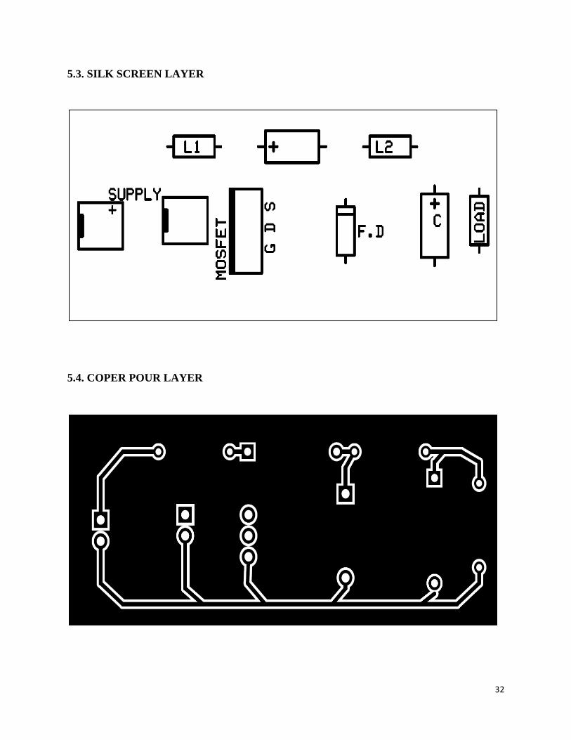
5.3. SILK SCREEN LAYER
5.4. COPER POUR LAYER