
Pentium PC Processor - Pro-face America...Features of the Pentium are highlighted below: • Full...
48
AT5+ Pentium PC Processor P/N 103626C 1998 XYCOM, INC. Printed in the United States of America
Transcript of Pentium PC Processor - Pro-face America...Features of the Pentium are highlighted below: • Full...

AT5+Pentium PC ProcessorP/N 103626C
1998 XYCOM, INC. Printed in the United States of America
Xycom Revision Record
Revision Description Date
A Manual Released 1/96B Manual Updated (incorporated PCN #207) 4/97C Manual Updated 7/98
Trademark InformationBrand or product names are registered trademarks of their respective owners.
Copyright InformationThis document is copyrighted by Xycom Incorporated (Xycom) and shall not be reproduced or copiedwithout expressed written authorization from Xycom.
The information contained within this document is subject to change without notice. Xycom does notguarantee the accuracy of the information and makes no commitment toward keeping it up to date.
xycomTechnical Publications Department750 North Maple RoadSaline, MI 48176–1292734 - 429-4971 (phone)734 - 429-1010 (fax)
i
Table of Contents
Chapter 1- Introduction
Product Overview ...................................................................................................................................1-1Features of the AT5+ CPU Board ..........................................................................................................1-1CPU ........................................................................................................................................................1-2AT Chipset ..............................................................................................................................................1-3VGA Controller........................................................................................................................................1-4Multifunction I/O Controller .....................................................................................................................1-5
Chapter 2- Board Configuration
Board Layout ..........................................................................................................................................2-1Jumpers ..................................................................................................................................................2-2
Disabling Functional Blocks.................................................................................................................2-3Battery-Backed RAM and Real-time Clock..........................................................................................2-3
Switch Settings .......................................................................................................................................2-3CPU Configurations................................................................................................................................2-5Memory Map...........................................................................................................................................2-4I/O Map ...................................................................................................................................................2-5System Interrupts....................................................................................................................................2-8Shadow RAM..........................................................................................................................................2-8Connectors .............................................................................................................................................2-8
Floppy Drive Connector (FDD and FDD-2)..........................................................................................2-8IDE Hard Drive Connectors (HDD-1) ...................................................................................................2-9COM1 Serial Port Connector ...............................................................................................................2-9COM2 Serial Port Connector ...............................................................................................................2-9VGA Connector ....................................................................................................................................2-9Port Connector (LPT1).........................................................................................................................2-9Keyboard (KYBD) ................................................................................................................................2-9Speaker Jack (SPKR) ..........................................................................................................................2-9Flat Panel (FPNL) ................................................................................................................................2-9
Chapter 3-BIOS Setup Menus
BIOS Overview .......................................................................................................................................3-1BIOS Main Setup Menu..........................................................................................................................3-1
System Time (HH/MM/SS)...................................................................................................................3-2System Date (MM:DD:YYYY) ..............................................................................................................3-2Diskette A or B .....................................................................................................................................3-3IDE Adapter 0 Master and Slave Sub-Menu........................................................................................3-3
Autotype Fixed Disk ..........................................................................................................................3-3Type...................................................................................................................................................3-3Cylinders............................................................................................................................................3-4Heads ................................................................................................................................................3-4

Table of Contents
ii
Chapter 3 - continued
Sectors/Track ....................................................................................................................................3-4Write Precomp...................................................................................................................................3-4Multi-Sector Transfers .......................................................................................................................3-4LBA Mode Control .............................................................................................................................3-432-Bit I/O ...........................................................................................................................................3-4Transfer Mode ...................................................................................................................................3-4
Memory Cache Sub-Menu ...................................................................................................................3-4External Cache..................................................................................................................................3-5Cache System BIOS Area.................................................................................................................3-5Cache Video BIOS Area....................................................................................................................3-5Cache Memory Region......................................................................................................................3-5
Memory Shadow Sub-Menu ................................................................................................................3-6Boot Sequence Sub-Menu...................................................................................................................3-6
Previous Boot ....................................................................................................................................3-7Boot Sequence..................................................................................................................................3-7Setup Prompt ....................................................................................................................................3-7POST Errors ......................................................................................................................................3-7Floppy Check ....................................................................................................................................3-7Summary Screen...............................................................................................................................3-7
Advanced Menu......................................................................................................................................3-8Integrated Peripherals Sub-Menu........................................................................................................3-9
COM Port...........................................................................................................................................3-9LPT Port ............................................................................................................................................3-9LPT Mode ..........................................................................................................................................3-9Diskette Controller .............................................................................................................................3-9Local Bus IDE Adapter ......................................................................................................................3-9
Advanced Chipset Control Sub-Menu ...............................................................................................3-10PCI Devices Sub-Menu......................................................................................................................3-11
Enable Master .................................................................................................................................3-11Default Latency Timer .....................................................................................................................3-11Latency Timer..................................................................................................................................3-12
Security Menu.......................................................................................................................................3-12Supervisor Password .........................................................................................................................3-12Set User Password ............................................................................................................................3-12Password on Boot ..............................................................................................................................3-13Diskette Access .................................................................................................................................3-13Fixed Disk Boot Sector ......................................................................................................................3-13System Backup Reminder/Virus Check Reminder ............................................................................3-13
Exit Menu..............................................................................................................................................3-13Save Values and Exit .........................................................................................................................3-14Exit Without Saving Changes ............................................................................................................3-14Get Default Values.............................................................................................................................3-14Load Previous Values ........................................................................................................................3-15Save Current Values..........................................................................................................................3-15
BIOS Compatibility................................................................................................................................3-15Battery-Backed RTC SRAM Usage......................................................................................................3-15
Appendix A - Pinouts

AT5+ Manual
iii
Appendix B - Installation of Additional DRAM
Appendix C - Installation of External Cache (COAST)
1-1
Chapter 1 – Introduction
Product Overview
The AT5+is based on a Pentium PC Processor. This highly integrated, eight-layerboard supports up to 64 Mbytes of fast page mode interleave DRAM, 256K externalcache in a COAST site, and provides an integrated floppy disk drive controller thatsupports up to two floppy disk drives. It also offers a high-performance, cost-effective integrated drive electronics (IDE) hard disk interface, two serial ports, oneparallel port, and a Super VGA controller with flat panel support.
Features of the AT5+ CPU Board
• CPU
• Pentium Processor
• Field upgradeable
• COAST cache modules supported (up to 256K)
• Two standard 72-pin SIMM sites support up to 64 Mbytes of DRAM
• Real-time clock with on-board battery backup
• Keyboard port
• 8.33 MHZ ATbus speed
• On-Board PCI Video Controller
• PCI bus super VGA graphics controller
• VGA analog output
• Flat panel driver circuitry
• Supports 8-bit monochrome, 16-bit passive colors (STN) and active color(TFT)
• Maximum resolution - 1024 x 768 with 256 colors
• I/O Controller
• PCI to ISA bus interface
• PCI enhanced IDE hard disk controller (supports two drives)
• Floppy disk (supports two drives)

AT5+ Manual
1-2
• Two 16550-compatible RS-232 serial ports
• One Centronics-compatible parallel port
CPU
Features of the Pentium are highlighted below:
• Full 64-bit internal architecture
• 8, 16, and 64-bit data types
• Eight general purpose 32-bit registers
• Object code compatible with 8086, 80186, 80286, 80386, and 80486 processors
• Runs MS-DOS, OS/2, UNIX, Windows NT, and Windows 95
• High-performance 64-bit data bus with 66 MHz clock
• Internal-bus speeds from 100 MHz to 233 MHz
• Integrated Memory Management Unit (MMU)
• Virtual memory support
• Optional on-chip paging
• Four levels of hardware-enforced protection
• Virtual 8086 mode allows executing 8086 Software in a protected and pagedsystem
• Large uniform address space
• 16 Mbyte physical
• 64 Terabyte virtual
• 4 Gigabyte maximum segment size
• On-chip debugging support including breakpoint registers
• On-chip 8 Kbyte instruction
• On-chip 8 Kbyte write back data cache
• Super scalar architecture
• Two pipeline integer units
• Capable under one clock cycle per instruction
• Pipelined floating - point unit

Chapter 1 - Introduction
1-3
AT Chipset
The Triton 82430 FX chipset—located at sites U14, U37, U33, and U34—providesthe following features:
• Pentium control logic and clocks support CPU speeds up to 66 MHZ with zero(or one) wait states
• PCI bus speeds up to 33 MHz (½ CPU external/speed)
• 146818-compatible real-time clock with 114 bytes of CMOS RAM
• Two 8237-compatible DMA controllers
• Two 8259-compatible interrupt controllers
• 8254-compatible programmable interval timer
• 82284-compatible clock generation and READY interface
• 82288-compatible bus controller
• DRAM controller that supports DRAM SIMM modules (1 Mbyte x 32,2 Mbyte x 32, 4 Mbyte x 32 and 8 Mbyte x 32)
• EDO supported
• Built-in PCI IDE controller
• DRAM refresh controller
• Four EMS page register (LIM EMS 4.0 and 3.2 compatible)
• Interface logic for an 8042 keyboard controller
• Interface logic for secondary cache
• Fast CPU Reset logic
AT5+ Manual
1-4
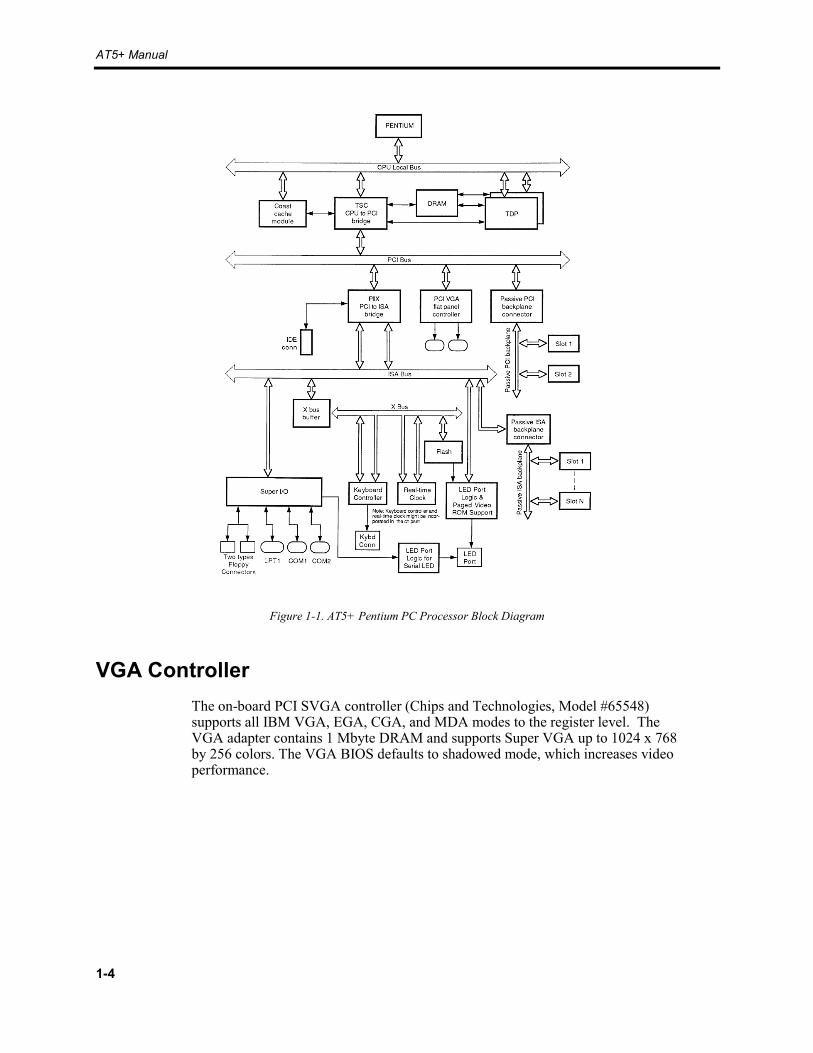
Figure 1-1. AT5+ Pentium PC Processor Block Diagram
VGA Controller
The on-board PCI SVGA controller (Chips and Technologies, Model #65548)supports all IBM VGA, EGA, CGA, and MDA modes to the register level. TheVGA adapter contains 1 Mbyte DRAM and supports Super VGA up to 1024 x 768by 256 colors. The VGA BIOS defaults to shadowed mode, which increases videoperformance.
Chapter 1 - Introduction
1-5
The VGA controller supports IBM modes 0-13h. In addition to these standard IBMmodes, the following Super VGA resolutions are supported:
• 132 x 25 text
• 132 x 50 text
• 800 x 600 x 16 colors
• 800 x 600 x 16 colors
• 1024 x 768 x 256 colors
• 640 x 400 x 256 colors
• 640 x 480 x 64K colors
• 640 x 480 x 16M colors
• 640 x 480 x 256 colors
• 800 x 600 x 256 colors
• 800 x 600 x 32K colors
A jumper is provided to disable the SVGA controller (refer to Chapter 2). This allowsother video adapters to be used.
Multifunction I/O Controller
The I/O controller provides the system's serial, parallel and floppy ports.

Chapter 2 - Board Configuration
2-1
Chapter 2 – Board Configuration
Board Layout
This chapter provides the information necessary to configure the AT5+. Thefollowing figure illustrates the layout of the board.
Figure 2- 1. AT5+ Board Layout
The following shows where the jumpers, connectors, and switches are located on theAT5+.
Figure 2- 2. AT5+ Jumpers, Connectors, and Switches

AT5+ Manual
2-2
Jumpers
The table below lists AT5+ jumpers, their default positions, and their functions (referto Figure 2-2).
AT5+ Jumpers
Jumper Position FunctionJ1 B
APentium CPUPentium MMX CPU
J2, J3, J4
CPU speed J2 J3 J4100/233 MHz A A A
133 MHz A A B
166 MHz B A B
200 MHz B A A
Core bus speed/external bus speed 7/2 or 3/2 - sets internal bus speed
Core bus speed/external bus speed 2x - sets internal bus speed
Core bus speed/external bus speed 5/2 - sets internal bus speed
Core bus speed/external bus speed 3x - sets internal bus speed
J5 A
B
M is the display enable signal
LP is the display enable signal
J6 AB
VGA enabledVGA disabled
J7 A
B
Intel Flash installed
AMD Flash installed
J8 A
B
Boot Flash enabled
AT boot enabled
J9 A
B
Parallel port set for IRQ7 (LPT 1)
Parallel port set for IRQ5 (LPT 2)
J10 A
B
ISP disable
ISP enable
J11 A
B
Orb ground not connected to logic ground
Orb ground connected to logic ground
J12, J13 J12 J13
A B
B A
A A
66 MHz frequency - external CPU bus frequency
60 MHz frequency - external CPU bus frequency
50 MHz frequency - external CPU bus frequency
J14, J15, J16 J14 J15 J16A A A
B B B
Pentium CPUPentium MMX CPU
indicates the default settings
Chapter 2 - Board Configuration
2-3
Disabling Functional Blocks
The SVGA controller can be disabled by moving jumper J6 to the B position. TheIDE and floppy drives and the parallel and COM ports can be disabled through theBIOS Setup Menus (refer to Chapter 3).
Battery-backed RAM and Real-time Clock
The AT5+ uses a self-contained, battery-backed real-time clock. The real-time clockis specified for 10 years of operation in the absence of power at 70°C. Switch SW1-1is used to clear CMOS memory.
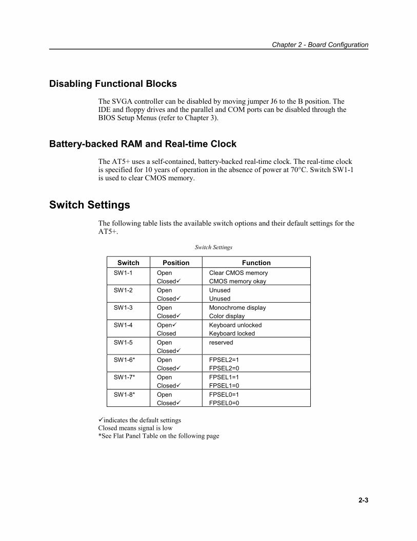
Switch Settings
The following table lists the available switch options and their default settings for theAT5+.
Switch Settings
Switch Position Function
SW1-1 OpenClosed
Clear CMOS memoryCMOS memory okay
SW1-2 OpenClosed
UnusedUnused
SW1-3 OpenClosed
Monochrome displayColor display
SW1-4 OpenClosed
Keyboard unlockedKeyboard locked
SW1-5 OpenClosed
reserved
SW1-6* OpenClosed
FPSEL2=1FPSEL2=0
SW1-7* OpenClosed
FPSEL1=1FPSEL1=0
SW1-8* OpenClosed
FPSEL0=1FPSEL0=0
indicates the default settingsClosed means signal is low*See Flat Panel Table on the following page
AT5+ Manual
2-4
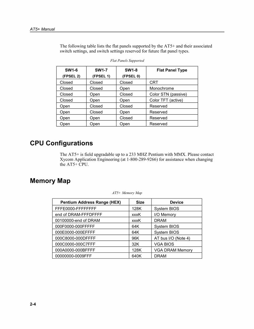
The following table lists the flat panels supported by the AT5+ and their associatedswitch settings, and switch settings reserved for future flat panel types.
Flat Panels Supported
SW1-6
(FPSEL 2)
SW1-7
(FPSEL 1)
SW1-8
(FPSEL 0)
Flat Panel Type
Closed Closed Closed CRT
Closed Closed Open Monochrome
Closed Open Closed Color STN (passive)
Closed Open Open Color TFT (active)
Open Closed Closed Reserved
Open Closed Open Reserved
Open Open Closed Reserved
Open Open Open Reserved
CPU Configurations
The AT5+ is field upgradable up to a 233 MHZ Pentium with MMX. Please contactXycom Application Engineering (at 1-800-289-9266) for assistance when changingthe AT5+ CPU.
Memory Map
AT5+ Memory Map
Pentium Address Range (HEX) Size Device
FFFE0000-FFFFFFFF 128K System BIOS
end of DRAM-FFFDFFFF xxxK I/O Memory
00100000-end of DRAM xxxK DRAM
000F0000-000FFFFF 64K System BIOS
000E0000-000EFFFF 64K System BIOS
000C8000-000DFFFF 96K AT bus I/O (Note 4)
000C0000-000C7FFF 32K VGA BIOS
000A0000-000BFFFF 128K VGA DRAM Memory
00000000-0009FFF 640K DRAM

Chapter 2 - Board Configuration
2-5
I/O Map
The AT5+ I/O map contains all IBM PC/AT architecture I/O ports, with someadditions. The AT5+ is shipped with serial ports 1 and 2 and parallel port 1 enabledat the address specified. Standard PC/AT I/O addresses are shown on the followingpage. Status/LED port bits, and CMOS RAM addresses are listed in the tables thatfollow.
I/O Address Map
Hex Range Device000-01F
020-021
022-023
025-02F
040-05F
060-06F
070-07F
080-091
93-9F
0A0-0BF
0C0-0DF
0F0
0F1
0F2-OFF
100
102
103-1EF
1F0-1F7
231
233
234
278-27F
280-2F7
2F8-2FF
300-36F
370-377
378-37F
380-3BF
3C0-3CF
3D0-3EF
3F0-3F7
3F8-3FF
CF8
CF9
CFC
DMA Controller 1, 8237A-5 equivalent
Interrupt Controller 1, 8259 equivalent
Available
Interrupt Controller 1, 8259 equivalent
Timer, 8254-2 equivalent
8742 equivalent (keyboard)
Real-time clock, bit 7 NMI mask
DMA page register
DMA page register
Interrupt controller 2,8259 equivalent
DMA controller 2,8237A-5 equivalent
N/A
N/A
N/A
Available
C&T Global enable register
Available
IDE controller (AT drive)
Xycom LED Port
Xycom Flash control register
Temperature sensor
Parallel Port 2
Available
Serial Port 2
Available
Alternate floppy disk controller
Parallel Port 1
Available
VGA/EGA2
Available
Primary floppy disk controller
Serial Port 1
PCI configuration address register
Reset Control Register
PCI configuration data register
AT5+ Manual
2-6
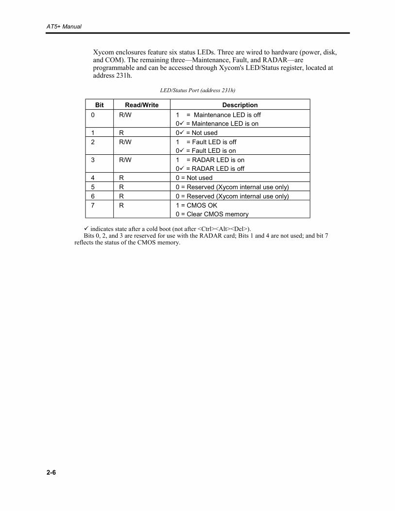
Xycom enclosures feature six status LEDs. Three are wired to hardware (power, disk,and COM). The remaining three—Maintenance, Fault, and RADAR—areprogrammable and can be accessed through Xycom's LED/Status register, located ataddress 231h.
LED/Status Port (address 231h)
Bit Read/Write Description
0 R/W 1 = Maintenance LED is off0 = Maintenance LED is on
1 R 0 = Not used
2 R/W 1 = Fault LED is off0 = Fault LED is on
3 R/W 1 = RADAR LED is on0 = RADAR LED is off
4 R 0 = Not used
5 R 0 = Reserved (Xycom internal use only)
6 R 0 = Reserved (Xycom internal use only)
7 R 1 = CMOS OK0 = Clear CMOS memory
indicates state after a cold boot (not after <Ctrl><Alt><Del>).Bits 0, 2, and 3 are reserved for use with the RADAR card; Bits 1 and 4 are not used; and bit 7
reflects the status of the CMOS memory.
Chapter 2 - Board Configuration
2-7
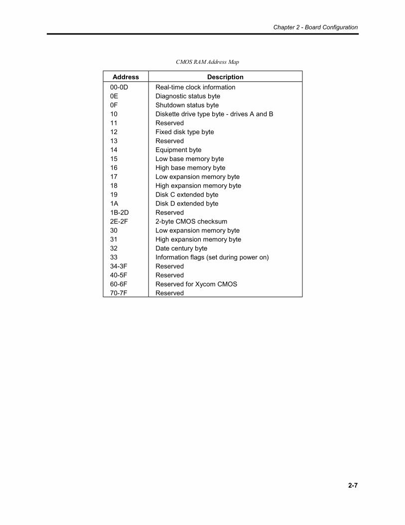
CMOS RAM Address Map
Address Description
00-0D0E0F101112131415161718191A1B-2D2E-2F3031323334-3F40-5F60-6F70-7F
Real-time clock informationDiagnostic status byteShutdown status byteDiskette drive type byte - drives A and BReservedFixed disk type byteReservedEquipment byteLow base memory byteHigh base memory byteLow expansion memory byteHigh expansion memory byteDisk C extended byteDisk D extended byteReserved2-byte CMOS checksumLow expansion memory byteHigh expansion memory byteDate century byteInformation flags (set during power on)ReservedReservedReserved for Xycom CMOSReserved
AT5+ Manual
2-8
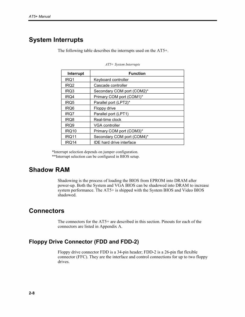
System Interrupts
The following table describes the interrupts used on the AT5+.
AT5+ System Interrupts
Interrupt Function
IRQ1 Keyboard controller
IRQ2 Cascade controller
IRQ3 Secondary COM port (COM2)*
IRQ4 Primary COM port (COM1)*
IRQ5 Parallel port (LPT2)*
IRQ6 Floppy drive
IRQ7 Parallel port (LPT1)
IRQ8 Real-time clock
IRQ9 VGA controller
IRQ10 Primary COM port (COM3)*
IRQ11 Secondary COM port (COM4)*
IRQ14 IDE hard drive interface
*Interrupt selection depends on jumper configuration.**Interrupt selection can be configured in BIOS setup.
Shadow RAM
Shadowing is the process of loading the BIOS from EPROM into DRAM afterpower-up. Both the System and VGA BIOS can be shadowed into DRAM to increasesystem performance. The AT5+ is shipped with the System BIOS and Video BIOSshadowed.
Connectors
The connectors for the AT5+ are described in this section. Pinouts for each of theconnectors are listed in Appendix A.
Floppy Drive Connector (FDD and FDD-2)
Floppy drive connector FDD is a 34-pin header; FDD-2 is a 26-pin flat flexibleconnector (FFC). They are the interface and control connections for up to two floppydrives.
Chapter 2 - Board Configuration
2-9
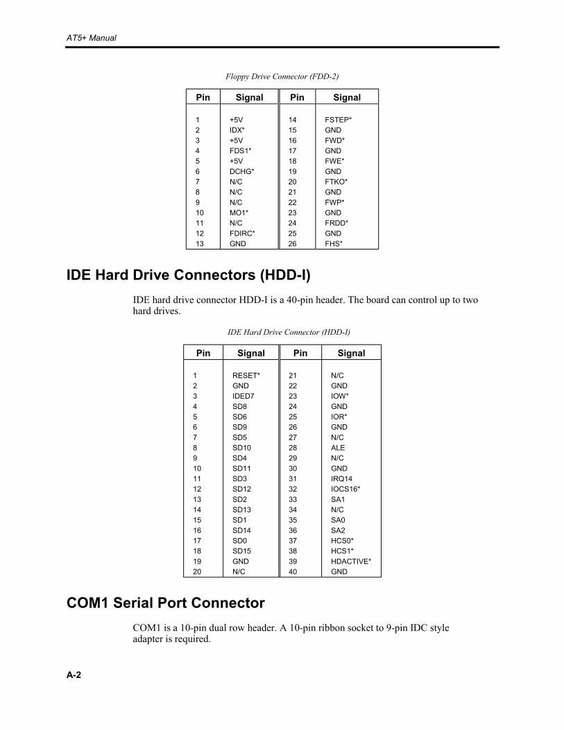
IDE Hard Drive Connectors (HDD-I)
IDE hard drive connector HDD-I is a 40-pin header. It is the control connector forany hard drive(s) interfaced with the AT5+. The board can control up to two harddrives.
COM1 Serial Port Connector (COM1)
COM1 is a 10-pin dual row header. A 10-pin ribbon socket to 9-pin IDC styleadapter is required. For more information, refer to the system manual.
COM2 Serial Port Connector (COM2)
COM2 is a 10-pin dual row header. A 10-pin ribbon socket to 9-pin IDC styleadapter is required. For more information, refer to the system manual.
VGA Connector (VGA)
The VGA connector is a 15-pin subminiature D style located on the bottom right ofthe board.
Port Connector (LPT1)
The Parallel port connector, LPT1, is a 25-pin female D subminiature connector.
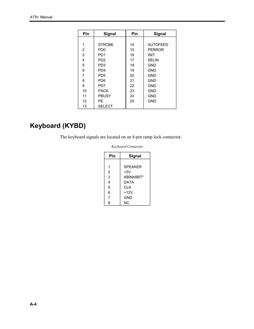
Keyboard (KYBD)
The keyboard signals are located on an 8-pin ramp lock connector.
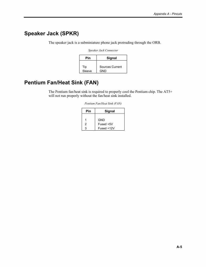
Speaker Jack (SPKR)
The speaker jack is a 2.5 mm phone jack protruding through the ORB drive cap.
Flat Panel (FPNL)
The flat panel connector is a 64-pin dual row header.
Chapter 3 - BIOS Setup Menus
3-1
Chapter 3 – BIOS Setup Menus
BIOS Overview
The AT5+ board’s customized BIOS has been designed to surpass the functionalityprovided for normal PC/ATs. This custom BIOS allows you to access the value-added features present on the AT5+ module without interfacing the hardwaredirectly.
General instructions for navigating through the screens are described below:
• ←↑↓→ moves the cursor up, down, left, and right. Pressing [Enter] validatesthe selection.
• [Esc] exits the menu. You are prompted to save any changes.
• [F5] selects the previous or smaller value.
• [F6] selects the next or higher value.
• [F9] automatically configures the system with the default values. These defaultvalues are defined by the system configuration and the values set in the SetupMenu.
NoteDisk drives must be configured via the IDE adapter menu.
• [F10] loads previous values.
BIOS Main Setup Menu
To start the BIOS Setup utility:
1. Press [F2] to enter SETUP
2. Press [F2] to display the Main Menu, which is depicted below:
AT5+ Manual
3-2
PhoenixBIOS Setup–Copyright 1992-94 Phoenix Technologies Ltd.Main Advanced Security Exit
Item Specific Help
System Time: [16:19:20]System Date: [03/02/95]Diskette A: [1.2 MB, 3.5”]Diskette B: [Not Installed]IDE Adapter 0 Master: C: 540 MbIDE Adapter 0 Slave: NoneVideo System: [EGA/VGA]Memory Cache:Memory Shadow: [Enabled]Boot sequence: [A: then C:]
System Memory: 640 KBExtended Memory: 31 MB
If the line item youare viewing hasspecific help, it willbe listed here.
F1 Help ↑↓ Select Item -/+ Change Values F9 Setup DefaultsESC Exit ←→ Select Menu Enter Select Sub–Menu F10 Previous Values
Figure 3- 1. Main Setup Menu
System Time (HH/MM/SS)
Sets the real-time clock for the month, day, and year.
The hour is calculated according to a 24-hour military clock, i.e., 00:00:00 through23:59:59. The left and right arrow keys and the [Enter] key may be used to movefrom one field to the next. The numeric keys, 0-9, are used to change the field values.It is not necessary to enter the seconds or type zeros in front of numbers.
System Date (MM:DD:YYYY)
Sets the real-time clock for the month, day, and year. The left and right arrow keysand the enter key may be used to move from one field to the next. The numeric keys,0-9, are used to change the field values. It is not necessary to type zeros in front ofnumbers.
Chapter 3 - BIOS Setup Menus
3-3
Diskette A or B
Select the floppy-disk drive installed in your system.
IDE Adapter 0 Master and Slave Sub-Menu
The IDE Adapter 0 Master and Slave sub-menus are used to configure the IDE harddrive information. If only one drive is attached to the IDE adapter, then only theparameters in the Master sub-menu needs to be entered. If two drives are connected,both Master and Slave sub-menu parameters will need to be entered. The Master andSlave sub-menus contain the same information.
IDE Adapter 0 Master (C: 540 Mb)
Item Specific Help
Autotype Fixed Disk: [Press Enter]Type: [User] 540 MbCylinders: [ 1048]Heads: [ 16]Sectors/Track: [ 63]Write Precomp: [None]
Multi-Sector Transfers: [16 Sectors]LBA Mode Control: [Enabled]32 Bit I/O: [Disabled]Transfer Mode: [Fast PIO 3]
If the line item you areviewing has specifichelp, it will be listedhere.
F1 Help ↑↓ Select Item -/+ Change Values F9 Setup DefaultsESC Exit ←→ Select Menu Enter Select Sub–Menu F10 Previous Values
Figure 3- 2. IDE Adapter Sub-Menu
Autotype Fixed Disk
Pressing <Enter> at this field attempts to read the hard disk parameters from thedrive itself, and sets “Type” field to “User” and allows editing of other fields. Youshould not attempt to manually set the disk drive parameters unless instructed to doso by Xycom Application Engineering.
Type
Options include 1 to 39, User or Auto. One to 39 fills in all remaining fields withvalues for predefined disk type. User prompts you to fill in remaining fields. Autoautotypes at each boot, displays settings in setup menus, and does not allow edit ofremaining fields.
AT5+ Manual
3-4
Cylinders
Number of cylinders on the hard drive. This information will be automaticallyentered when using the Autotype Fixed Disk option above.
Heads
Number of read/write heads on the hard drive. This information will be automaticallyentered when using the Autotype Fixed Disk option above.
Sectors/Track
Number of sectors per track on the hard drive. This information will be automaticallyentered when using the Autotype Fixed Disk option above.
Write Precomp
This value is not used or required by IDE hard drives.
Multi-Sector Transfers
Options are Auto, 2, 4, 8, or 16 sectors. Auto sets the number of sectors per block atthe highest number supported by the drive.
LBA Mode Control
Enables Logical Block Access. Default is disabled and should work with most harddrives.
32-Bit I/O
Enables 32-bit communication between CPU and IDE interface.
Transfer Mode
Selects the method for transferring the data between the hard disk and systemmemory.
Memory Cache Sub-Menu
Enabling cache increases CPU performance by holding data most recently accessedin a special high-speed static RAM area called cache. The AT5+ provides two levelsof cache memory; level one is 16K internal to the Pentium processor, and level twoor external cache is the cache on a stick site (COAST) which can accommodate 256Kof high-speed cache memory.
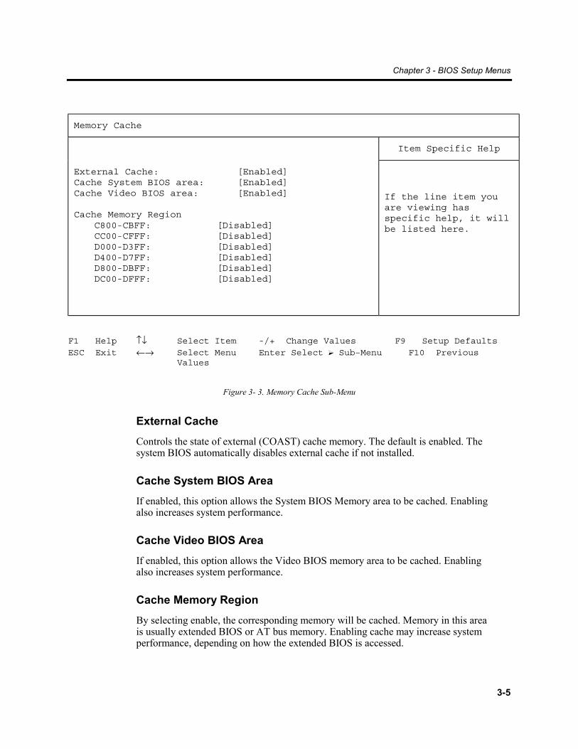
Chapter 3 - BIOS Setup Menus
3-5
Memory Cache
Item Specific Help
External Cache: [Enabled]Cache System BIOS area: [Enabled]Cache Video BIOS area: [Enabled]
Cache Memory RegionC800-CBFF: [Disabled]CC00-CFFF: [Disabled]D000-D3FF: [Disabled]D400-D7FF: [Disabled]D800-DBFF: [Disabled]DC00-DFFF: [Disabled]
If the line item youare viewing hasspecific help, it willbe listed here.
F1 Help ↑↓ Select Item -/+ Change Values F9 Setup DefaultsESC Exit ←→ Select Menu Enter Select Sub–Menu F10 Previous
Values
Figure 3- 3. Memory Cache Sub-Menu
External Cache
Controls the state of external (COAST) cache memory. The default is enabled. Thesystem BIOS automatically disables external cache if not installed.
Cache System BIOS Area
If enabled, this option allows the System BIOS Memory area to be cached. Enablingalso increases system performance.
Cache Video BIOS Area
If enabled, this option allows the Video BIOS memory area to be cached. Enablingalso increases system performance.
Cache Memory Region
By selecting enable, the corresponding memory will be cached. Memory in this areais usually extended BIOS or AT bus memory. Enabling cache may increase systemperformance, depending on how the extended BIOS is accessed.

AT5+ Manual
3-6
Memory Shadow Sub-Menu
This field displays the amount of shadow memory in use. The contents of this fieldare controlled by BIOS shadow selection. Shadow memory is used to copy thesystem and/or Video BIOS into RAM to improve performance. The AT5+ allocatesShadow RAM in Kbytes, and this number will be displayed on the menu. This field,which is not editable, is for reference only.
The AT5+ is shipped with the System BIOS and Video BIOS shadowed.
Memory Shadow
Item Specific Help
System Shadow: EnabledVideo Shadow: [Enabled] If the line item you
are viewing hasspecific help, it willbe listed here.
F1 Help ↑↓ Select Item -/+ Change Values F9 Setup DefaultsESC Exit ←→ Select Menu Enter Select Sub–Menu F10 Previous Values
Figure 3- 4. Memory Shadow Sub-Menu
Boot Sequence Sub-Menu
This menu allows the boot sequence to be configured.
Boot Sequence
Item Specific Help
Previous Boot [Disabled]Boot sequence: [A: then C:]Setup prompt: [Disabled]POST Errors: [Enabled]Floppy check: [Enabled]Summary screen: [Enabled]
If the line item youare viewing hasspecific help, it willbe listed here.
F1 Help ↑↓ Select Item -/+ Change Values F9 Setup DefaultsESC Exit ←→ Select Menu Enter Select Sub–Menu F10 Previous Values
Figure 3- 5. Boot Options Sub-Menu
Chapter 3 - BIOS Setup Menus
3-7
Previous Boot
This option is disabled. If this option is enabled, the System BIOS can detect if a bootsequence was not completed properly. This condition may be caused by a powerfailure, or reset during boot-up, or invalid CMOS configuration. If the BIOS detectsthis condition, the following message will be displayed, “Previous bootincomplete - default configuration used.” The system will berebooted using the default configuration.
If this option is disabled, the system BIOS will not detect incomplete boot and youwill not be notified.
Boot Sequence
The BIOS attempts to load the operating system from the disk drives in the sequenceselected here.
Setup Prompt
This option is disabled. If enabled, the system will display “Press <F2> forSetup” during boot up.
POST Errors
If enabled, the system will halt if it encounters a boot error and display “Press<F1> to resume, <F2> for Setup”.
Floppy Check
If enabled, the system seeks diskette drives during boot up. Disabling speeds boottime.
Summary Screen
If enabled, displays system summary screen during boot up.
AT5+ Manual
3-8
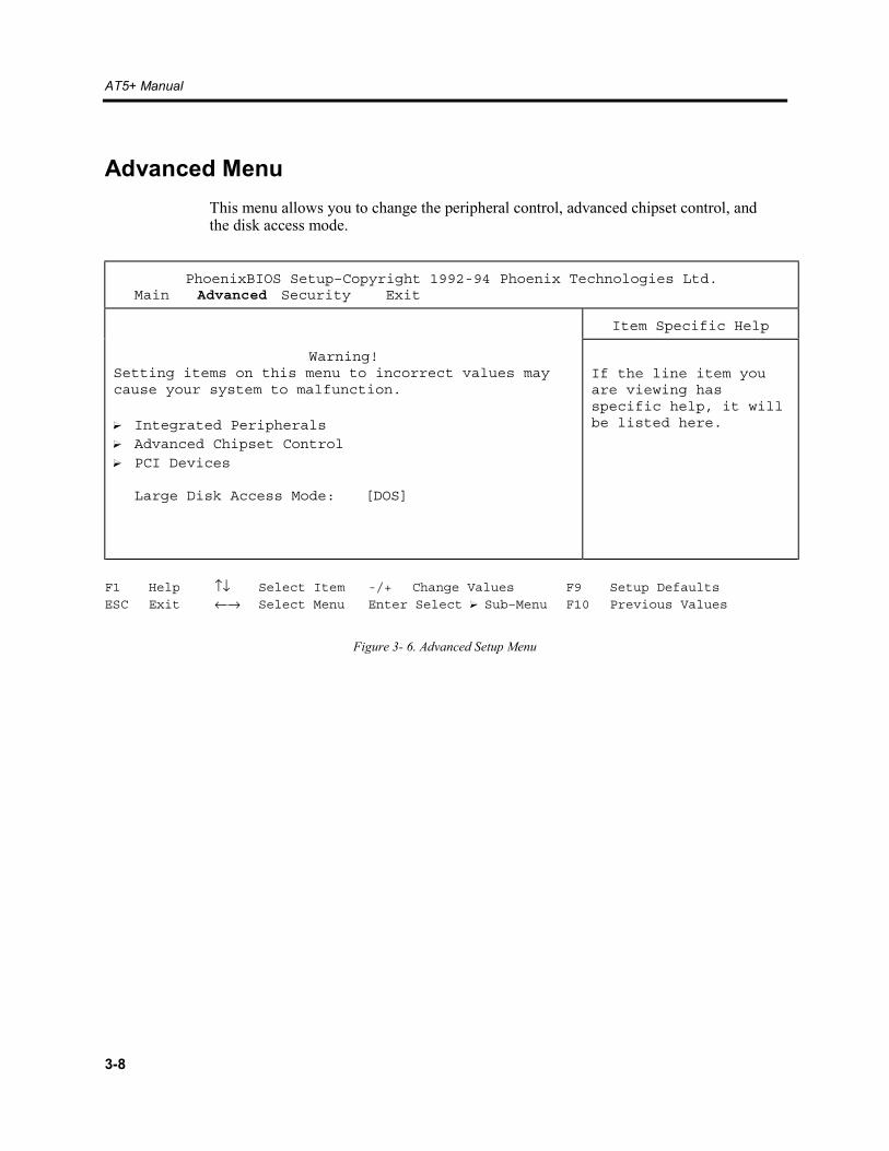
Advanced Menu
This menu allows you to change the peripheral control, advanced chipset control, andthe disk access mode.
PhoenixBIOS Setup–Copyright 1992-94 Phoenix Technologies Ltd.Main Advanced Security Exit
Item Specific Help
Warning!Setting items on this menu to incorrect values maycause your system to malfunction.
Integrated PeripheralsAdvanced Chipset ControlPCI Devices
Large Disk Access Mode: [DOS]
If the line item youare viewing hasspecific help, it willbe listed here.
F1 Help ↑↓ Select Item -/+ Change Values F9 Setup DefaultsESC Exit ←→ Select Menu Enter Select Sub–Menu F10 Previous Values
Figure 3- 6. Advanced Setup Menu
Chapter 3 - BIOS Setup Menus
3-9
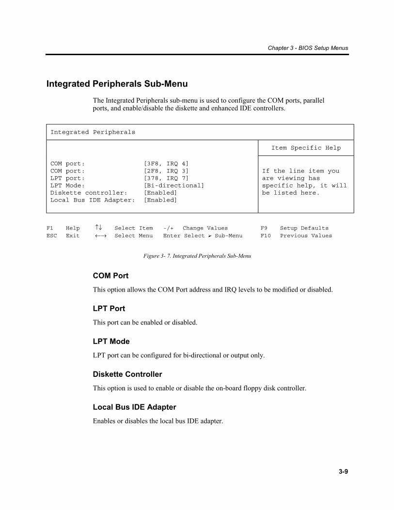
Integrated Peripherals Sub-Menu
The Integrated Peripherals sub-menu is used to configure the COM ports, parallelports, and enable/disable the diskette and enhanced IDE controllers.
Integrated Peripherals
Item Specific Help
COM port: [3F8, IRQ 4]COM port: [2F8, IRQ 3]LPT port: [378, IRQ 7]LPT Mode: [Bi-directional]Diskette controller: [Enabled]Local Bus IDE Adapter: [Enabled]
If the line item youare viewing hasspecific help, it willbe listed here.
F1 Help ↑↓ Select Item -/+ Change Values F9 Setup DefaultsESC Exit ←→ Select Menu Enter Select Sub–Menu F10 Previous Values
Figure 3- 7. Integrated Peripherals Sub-Menu
COM Port
This option allows the COM Port address and IRQ levels to be modified or disabled.
LPT Port
This port can be enabled or disabled.
LPT Mode
LPT port can be configured for bi-directional or output only.
Diskette Controller
This option is used to enable or disable the on-board floppy disk controller.
Local Bus IDE Adapter
Enables or disables the local bus IDE adapter.

AT5+ Manual
3-10
Advanced Chipset Control Sub-Menu
This menu can be used to change the values in the chipset registers and optimize yoursystem’s performance.
Advanced Chipset Control
Item Specific Help
DRAM Speed [60ns]DMA Aliasing: [Enabled]8-bit I/O Recovery [4.5]16-bit I/O Recovery [4.5]IRQ12 used by: [ISA bus]
If the line item youare viewing hasspecific help, it willbe listed here.
F1 Help ↑↓ Select Item -/+ Change Values F9 Setup DefaultsESC Exit ←→ Select Menu Enter Select Sub–Menu F10 Previous Values
Figure 3- 8. Advanced Chipset Control Sub-Menu
Chapter 3–BIOS Setup Menus
3-11
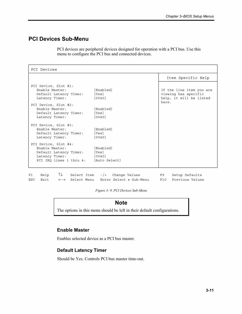
PCI Devices Sub-Menu
PCI devices are peripheral devices designed for operation with a PCI bus. Use thismenu to configure the PCI bus and connected devices.
PCI Devices
Item Specific Help
PCI Device, Slot #1:Enable Master: [Enabled]Default Latency Timer: [Yes]Latency Timer: [0040]
PCI Device, Slot #2:Enable Master: [Enabled]Default Latency Timer: [Yes]Latency Timer: [0040]
PCI Device, Slot #3:Enable Master: [Enabled]Default Latency Timer: [Yes]Latency Timer: [0040]
PCI Device, Slot #4:Enable Master: [Enabled]Default Latency Timer: [Yes]Latency Timer: [0040]PCI IRQ lines 1 thru 4: [Auto Select]
If the line item you areviewing has specifichelp, it will be listedhere.
F1 Help ↑↓ Select Item -/+ Change Values F9 Setup DefaultsESC Exit ←→ Select Menu Enter Select Sub–Menu F10 Previous Values
Figure 3- 9. PCI Devices Sub-Menu
NoteThe options in this menu should be left in their default configurations.
Enable Master
Enables selected device as a PCI bus master.
Default Latency Timer
Should be Yes. Controls PCI bus master time-out.
AT5+ Manual
3-12
Latency Timer
Displays the current value of latency timer.
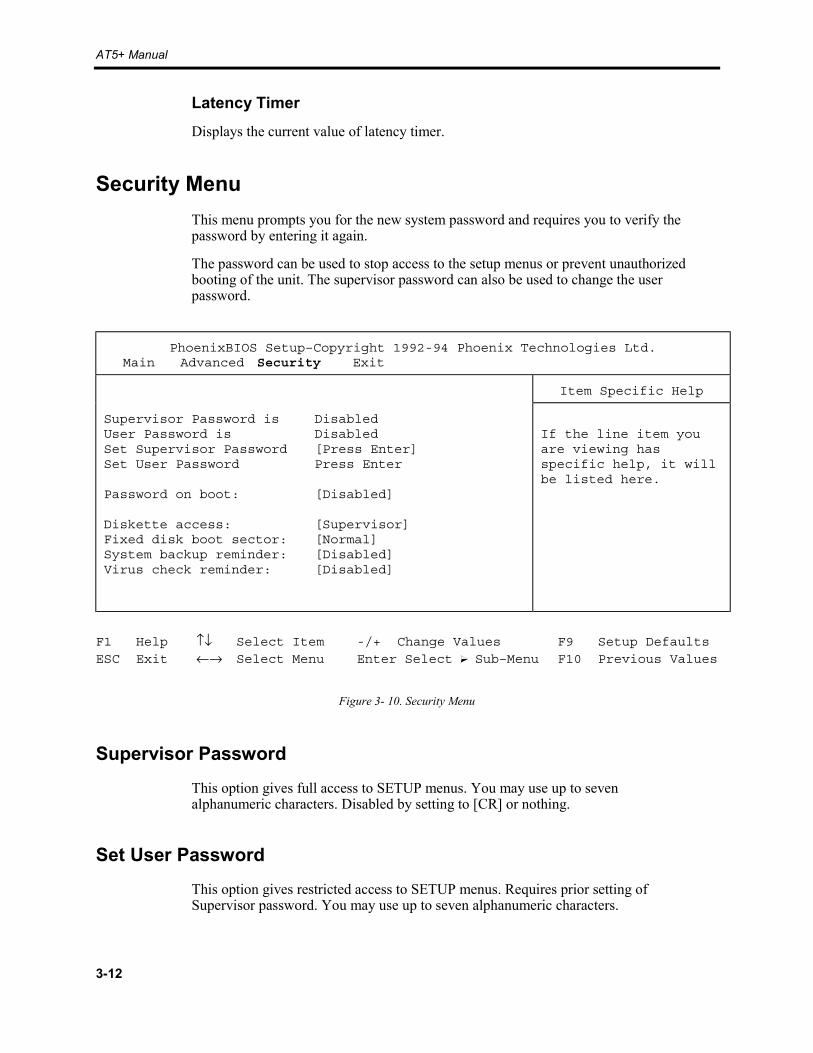
Security Menu
This menu prompts you for the new system password and requires you to verify thepassword by entering it again.
The password can be used to stop access to the setup menus or prevent unauthorizedbooting of the unit. The supervisor password can also be used to change the userpassword.
PhoenixBIOS Setup–Copyright 1992-94 Phoenix Technologies Ltd.Main Advanced Security Exit
Item Specific Help
Supervisor Password is DisabledUser Password is DisabledSet Supervisor Password [Press Enter]Set User Password Press Enter
Password on boot: [Disabled]
Diskette access: [Supervisor]Fixed disk boot sector: [Normal]System backup reminder: [Disabled]Virus check reminder: [Disabled]
If the line item youare viewing hasspecific help, it willbe listed here.
F1 Help ↑↓ Select Item -/+ Change Values F9 Setup DefaultsESC Exit ←→ Select Menu Enter Select Sub–Menu F10 Previous Values
Figure 3- 10. Security Menu
Supervisor Password
This option gives full access to SETUP menus. You may use up to sevenalphanumeric characters. Disabled by setting to [CR] or nothing.
Set User Password
This option gives restricted access to SETUP menus. Requires prior setting ofSupervisor password. You may use up to seven alphanumeric characters.
Chapter 3–BIOS Setup Menus
3-13
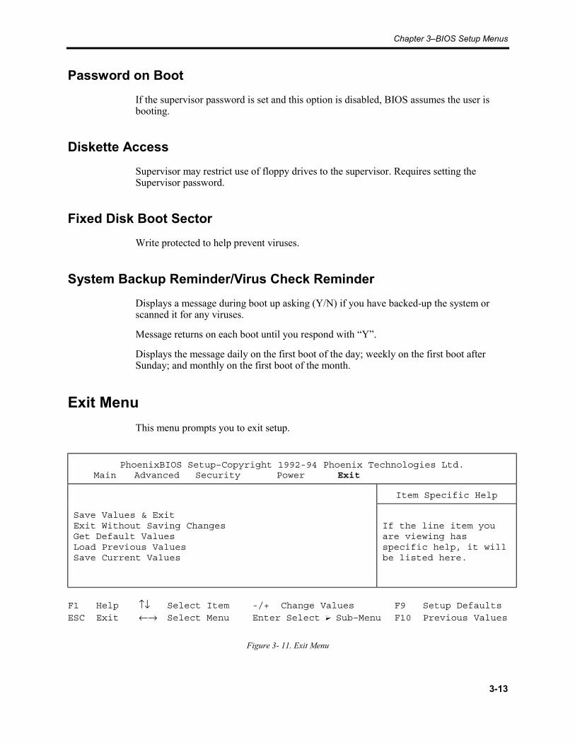
Password on Boot
If the supervisor password is set and this option is disabled, BIOS assumes the user isbooting.
Diskette Access
Supervisor may restrict use of floppy drives to the supervisor. Requires setting theSupervisor password.
Fixed Disk Boot Sector
Write protected to help prevent viruses.
System Backup Reminder/Virus Check Reminder
Displays a message during boot up asking (Y/N) if you have backed-up the system orscanned it for any viruses.
Message returns on each boot until you respond with “Y”.
Displays the message daily on the first boot of the day; weekly on the first boot afterSunday; and monthly on the first boot of the month.
Exit Menu
This menu prompts you to exit setup.
PhoenixBIOS Setup–Copyright 1992-94 Phoenix Technologies Ltd.Main Advanced Security Power Exit
Item Specific Help
Save Values & ExitExit Without Saving ChangesGet Default ValuesLoad Previous ValuesSave Current Values
If the line item youare viewing hasspecific help, it willbe listed here.
F1 Help ↑↓ Select Item -/+ Change Values F9 Setup DefaultsESC Exit ←→ Select Menu Enter Select Sub–Menu F10 Previous Values
Figure 3- 11. Exit Menu
AT5+ Manual
3-14
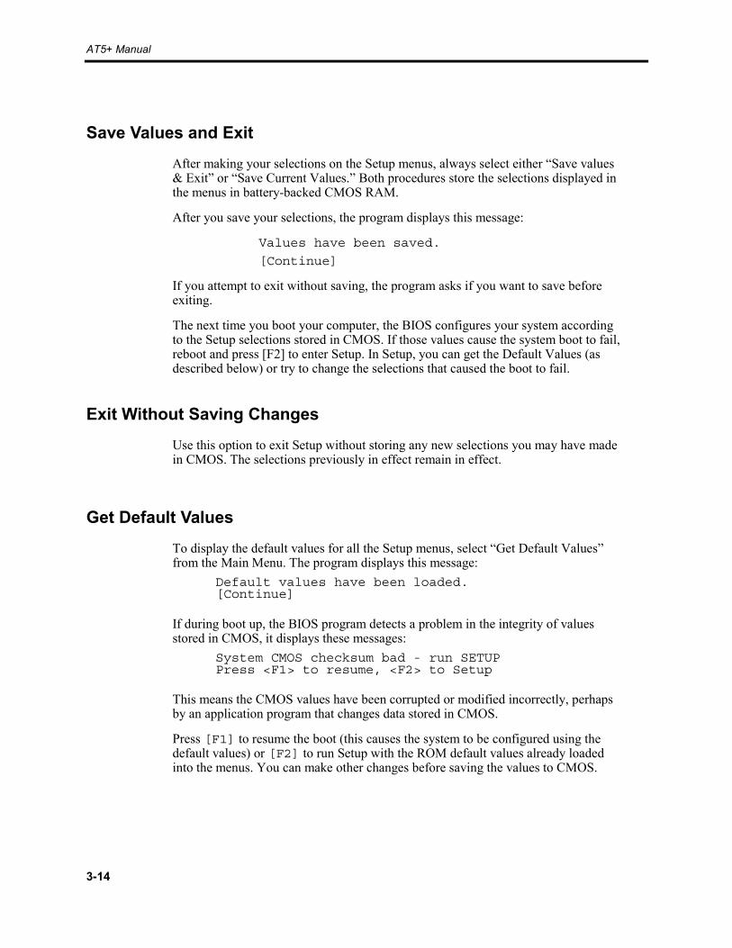
Save Values and Exit
After making your selections on the Setup menus, always select either “Save values& Exit” or “Save Current Values.” Both procedures store the selections displayed inthe menus in battery-backed CMOS RAM.
After you save your selections, the program displays this message:
Values have been saved.
[Continue]
If you attempt to exit without saving, the program asks if you want to save beforeexiting.
The next time you boot your computer, the BIOS configures your system accordingto the Setup selections stored in CMOS. If those values cause the system boot to fail,reboot and press [F2] to enter Setup. In Setup, you can get the Default Values (asdescribed below) or try to change the selections that caused the boot to fail.
Exit Without Saving Changes
Use this option to exit Setup without storing any new selections you may have madein CMOS. The selections previously in effect remain in effect.
Get Default Values
To display the default values for all the Setup menus, select “Get Default Values”from the Main Menu. The program displays this message:
Default values have been loaded.[Continue]
If during boot up, the BIOS program detects a problem in the integrity of valuesstored in CMOS, it displays these messages:
System CMOS checksum bad - run SETUPPress <F1> to resume, <F2> to Setup
This means the CMOS values have been corrupted or modified incorrectly, perhapsby an application program that changes data stored in CMOS.
Press [F1] to resume the boot (this causes the system to be configured using thedefault values) or [F2] to run Setup with the ROM default values already loadedinto the menus. You can make other changes before saving the values to CMOS.

Chapter 3–BIOS Setup Menus
3-15
Load Previous Values
If, during a Setup Session, you change your mind about changes you have made andhave not yet saved the values to CMOS, you can restore the values you previouslysaved to CMOS.
Selecting Load Previous Values on the Exit menu updates all the selections anddisplays this message:
Previous values have been loaded.[Continue]
Save Current Values
This option saves all the selections without exiting Setup. You can return to the othermenus if you want to review and change your selections.
BIOS Compatibility
This BIOS is IBM PC/AT compatible with additional CMOS RAM and BIOS dataareas used.
Battery-Backed RTC SRAM Usage
This BIOS uses the standard PC/AT battery-backed RTC SRAM. In addition, thefollowing locations are used as indicated:
Address Bit(s) Description
62h
6E6FH
0-3
0-7
Reserved (set to 000b).Backlight blanking timeout:0000b:none0001b:5 minutes...1111b:75 minutesXycom Configuration Checksum

A-1
Appendix A – Pinouts
This appendix describes the pinouts for the AT5+ connectors defined in Chapter 2.
Floppy Drive Connector (FDD and FDD-2)
Floppy drive connector FDD is a 34-pin header; FDD-2 is a 26-pin flat flexibleconnector (FFC). They are the interface and control connections for up to two floppydrives.
Floppy Drive Connector (FDD)
Pin Signal Pin
Signal
1
2
3
4
5
6
7
8
9
10
11
12
13
14
15
16
17
GND
FRWC*
GND
N/C
KEY
N/C
GND
IDX*
GND
MO1*
GND
FDS2*
GND
FDS1*
GND
MO2*
GND
18
19
20
21
22
23
24
25
26
27
28
29
30
31
32
33
34
FDIRC*
GND
FSTEP*
GND
FWD*
GND
FWE*
GND
FTK0*
GND
FWP*
GND
FRDD*
GND
FHS*
GND
DCHG*
AT5+ Manual
A-2
Floppy Drive Connector (FDD-2)
Pin Signal Pin Signal
1
2
3
4
5
6
7
8
9
10
11
12
13
+5V
IDX*
+5V
FDS1*
+5V
DCHG*
N/C
N/C
N/C
MO1*
N/C
FDIRC*
GND
14
15
16
17
18
19
20
21
22
23
24
25
26
FSTEP*
GND
FWD*
GND
FWE*
GND
FTKO*
GND
FWP*
GND
FRDD*
GND
FHS*
IDE Hard Drive Connectors (HDD-I)
IDE hard drive connector HDD-I is a 40-pin header. The board can control up to twohard drives.
IDE Hard Drive Connector (HDD-I)
Pin Signal Pin Signal
1
2
3
4
5
6
7
8
9
10
11
12
13
14
15
16
17
18
19
20
RESET*
GND
IDED7
SD8
SD6
SD9
SD5
SD10
SD4
SD11
SD3
SD12
SD2
SD13
SD1
SD14
SD0
SD15
GND
N/C
21
22
23
24
25
26
27
28
29
30
31
32
33
34
35
36
37
38
39
40
N/C
GND
IOW*
GND
IOR*
GND
N/C
ALE
N/C
GND
IRQ14
IOCS16*
SA1
N/C
SA0
SA2
HCS0*
HCS1*
HDACTIVE*
GND
COM1 Serial Port Connector
COM1 is a 10-pin dual row header. A 10-pin ribbon socket to 9-pin IDC styleadapter is required.

Appendix A - Pinouts
A-3
COM1 Serial Port Connector
Pin Signal Pin Signal
12345
DCD1DSR1RXD1RTS1TXD1
678910
CTS1DTR1RI1GNDNO CONNECT
COM2 Serial Port Connector
COM2 is a 10-pin dual row header. A 10-pin ribbon socket to 9-pin IDC styleadapter is required.
COM2 Serial Port Connector
Pin Signal Pin Signal
12345
DCD2DSR2RXD2RTS2TXD2
678910
CTS2DTR2RI2GNDNO CONNECT
VGA Connector
The VGA connector is a 15-pin subminiature located on the bottom right of theboard.
VGA Connector
Pin Signal Pin Signal
12345678
REDGREENBLUEN/CGNDGNDGNDGND
9101112131415
KEYGNDN/CN/CHSYNCVSYNCN/C
Parallel Port Connector (LPT1)
The Parallel port connector, LPT1, is a 25-pin female D subminiature connector.
Parallel Port Connector
AT5+ Manual
A-4
Pin Signal Pin Signal
12345678910111213
STROBEPD0PD1PD2PD3PD4PD5PD6PD7PACKPBUSYPESELECT
141516171819202122232425
AUTOFEEDPERRORINITSELINGNDGNDGNDGNDGNDGNDGNDGND
Keyboard (KYBD)
The keyboard signals are located on an 8-pin ramp lock connector.
Keyboard Connector
Pin Signal
12345678
SPEAKER+5VKBINHIBIT*DATACLK+12VGNDNC
Appendix A - Pinouts
A-5
Speaker Jack (SPKR)
The speaker jack is a subminiature phone jack protruding through the ORB.
Speaker Jack Connector
Pin Signal
TipSleeve
Sources CurrentGND
Pentium Fan/Heat Sink (FAN)
The Pentium fan/heat sink is required to properly cool the Pentium chip. The AT5+will not run properly without the fan/heat sink installed.
Pentium Fan/Heat Sink (FAN)
Pin Signal
123
GNDFused +5VFused +12V

AT5+ Manual
A-6
Flat Panel Connector (FPNL)
The flat panel connector is a 64-pin dual row header.
Flat Panel Connector
Pin Signal Pin Signal1 GND 33 GND
2 MAINT LED 34 FP11
3 FAULT LED 35 GND
4 SERIAL LED 36 BLANK
5 DRIVE LED 37 GND
6 RADAR LED 38 SHFCLK
7 GND 39 GND
8 KB CLOCK 40 LP
9 GND 41 GND
10 RESET* 42 FLM
11 GND 43 GND
12 ENAVDD* 44 ACDCLK
13 GND 45 GND
14 ENAVEE* 46 FP17
15 GND 47 FP18
16 FP0 48 FP19
17 FP1 49 FP20
18 FP2 50 GND
19 FP3 51 FP21
20 GND 52 FP22
21 FP4 53 FP23
22 FP5 54 FP24
23 FP6 55 GND
24 FP7 56 N/C
25 GND 57 N/C
26 FP8 58 N/C
27 GND 59 N/C
28 FP9 60 N/C
29 GND 61 N/C
30 FP10 62 N/C
31 GND 63 N/C
32 FP11 64 GND
B-1
Appendix B – Installation of Additional DRAM
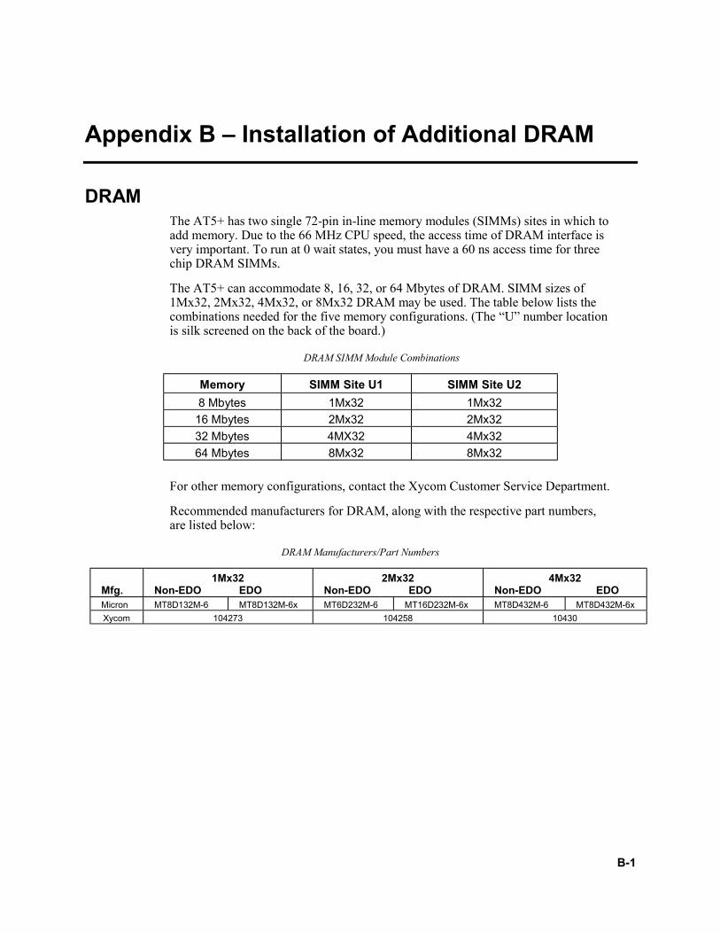
DRAMThe AT5+ has two single 72-pin in-line memory modules (SIMMs) sites in which toadd memory. Due to the 66 MHz CPU speed, the access time of DRAM interface isvery important. To run at 0 wait states, you must have a 60 ns access time for threechip DRAM SIMMs.
The AT5+ can accommodate 8, 16, 32, or 64 Mbytes of DRAM. SIMM sizes of1Mx32, 2Mx32, 4Mx32, or 8Mx32 DRAM may be used. The table below lists thecombinations needed for the five memory configurations. (The “U” number locationis silk screened on the back of the board.)
DRAM SIMM Module Combinations
Memory SIMM Site U1 SIMM Site U2
8 Mbytes 1Mx32 1Mx32
16 Mbytes 2Mx32 2Mx32
32 Mbytes 4MX32 4Mx32
64 Mbytes 8Mx32 8Mx32
For other memory configurations, contact the Xycom Customer Service Department.
Recommended manufacturers for DRAM, along with the respective part numbers,are listed below:
DRAM Manufacturers/Part Numbers
Mfg.1Mx32
Non-EDO EDO2Mx32
Non-EDO EDO4Mx32
Non-EDO EDOMicron MT8D132M-6 MT8D132M-6x MT6D232M-6 MT16D232M-6x MT8D432M-6 MT8D432M-6x
Xycom 104273 104258 10430
AT5+ Manual
B-2
Dram Installation
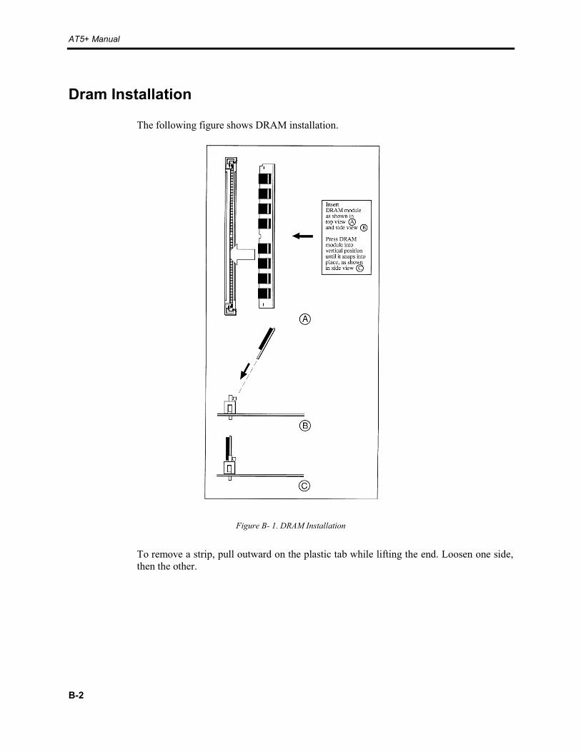
The following figure shows DRAM installation.
Figure B- 1. DRAM Installation
To remove a strip, pull outward on the plastic tab while lifting the end. Loosen one side,then the other.
C-1
Appendix C – Installation of External Cache(COAST)
External CacheThe Xycom AT5+ provides support for 256K of cache in socket U3, cache on a sticksite (COAST). AT5+ external cache is supplied on a printed circuit board similar tothe DRAM modules. This printed circuit board is designed to plug into the socket atU3, which is next to the two DRAM sockets.
To install the cache, line up the COAST module with the socket and apply lightsteady pressure until the COAST module is seated. The socket is keyed so that themodule can only be plugged into the correct orientation.
Recommended manufacturers for the COAST modules used in the AT5+, along withthe respective part numbers, are listed below:
COAST Manufacturers/Part Numbers
Mfg. Cache 256K Synchronous 66 MHz(COAST)
Corsair C53Q256K3C
1st Tech. 29-256-05
Xycom 104330
AT5+ Manual
C-2
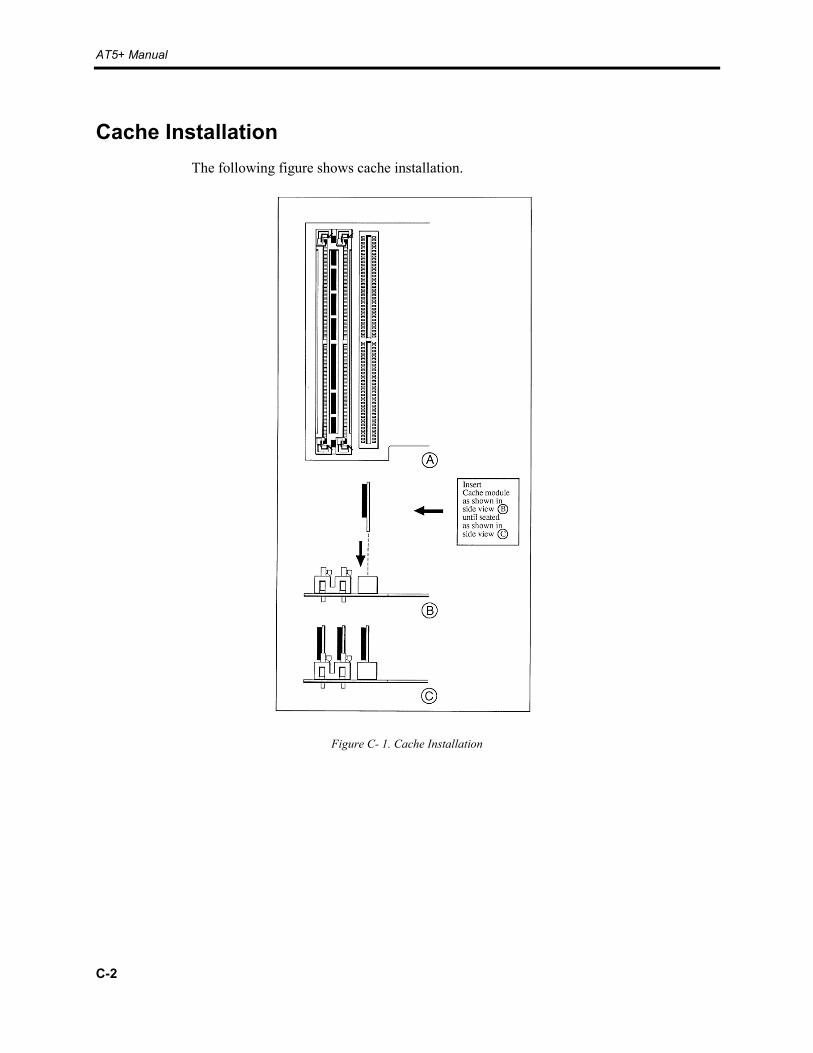
Cache Installation
The following figure shows cache installation.
Figure C- 1. Cache Installation
Index-1
Index
AAT chipset, 1-3advanced menu, 3-8
advanced chipset control, 3-10integrated peripherals, 3-9PCI devices, 3-11
BBIOS compatibility, 3-15BIOS main setup menu, 3-2
boot sequence, 3-6diskette A or B, 3-3IDE adapter 0 master, 3-3memory cache, 3-4memory shadow, 3-6system date, 3-2system time, 3-2
battery-backed RAM and real-time clock, 2-3battery-backed RTC SRAM usage, 3-15board layout, 2-1boot sequence sub-menu, 3-6
Ccache, Appendix CCMOS RAM address map, 2-7COAST, Appendix CCOM1, 2-9COM2, 2-9CPU, 1-2CPU configurations, 2-4chipset, 1-3configurations, 2-1connectors, 2-8
COM1, 2-9, Appendix ACOM2, 2-9, Appendix Aflat panel, 2-9floppy drive, 2-8IDE hard drive, 2-9
keyboard, 2-9port (LPT1), 2-9
speaker jack, 2-9VGA, 2-9
DDRAM installation, Appendix B
default settingsjumpers, 2-2switches, 2-3
disabling functional blocks, 2-3
Eexit menu, 3-13
exit without saving, 3-14get default values, 3-14load previous values, 3-15save current values, 3-15save values and exit, 3-14
Ffeatures, 1-1, 1-2flat panel connector, 2-9, A-6floppy drive connector, 2-8, A-1
II/O address map, 2-5I/O controller, 1-5I/O port addresses, 2-5IDE adapter 0 master and slave, 3-3IDE hard drive connectors, 2-9, A-2installation of external cache (COAST), C-1installation of DRAM, B-1, B-2integrated peripherals, 3-9
Jjumpers, 2-2
LLED/status port, 2-6
Mmemory cache sub-menu, 3-4memory map, 2-4memory shadow sub-menu, 3-6multifunction I/O controller, 1-5
PPCI devices sub-menu, 3-11parallel port connector, A-5pinouts, Appendix A
AT5+ Manual
Index-2
Pentium fan/heat sink, A-6
Ssecurity menu, 3-12
diskette access, 3-13fixed disk boot sector, 3-13password on boot, 3-13set user password, 3-12supervisor password, 3-12system backup/virus check, 3-13
serial port connectors, 2-9
shadow RAM, 2-8speaker jack connector, 2-9, A-5switch settings, 2-3switches, 2-3system interrupts, 2-8
VVGA controller, 1-4VGA connector, 2-9, A-3

Index
Index-3


![A High-Speed 64-Bit Binary Comparator€¦ · A high-speed 64-bit binary comparator 39 | Page III. EXISTING 64-BIT BINARY COMPARATOR DESIGN 64-bit comparator in reference [8], [9],](https://static.fdocuments.us/doc/165x107/5eac1a458d19873e777698b4/a-high-speed-64-bit-binary-comparator-a-high-speed-64-bit-binary-comparator-39-.jpg)


