
Shedding light on fractals: Exploration of the...
134
Ting Lee Chen Shedding light on fractals: Exploration of the Sierpinski carpet optical antenna
Transcript of Shedding light on fractals: Exploration of the...

Ting Lee Chen
Shedding light on fractals:
Exploration of the
Sierpinski carpet optical antenna

SHEDDING LIGHT ON FRACTALS:
EXPLORATION OF THE
SIERPINSKI CARPET OPTICAL ANTENNA

Thesis committee members
Supervisor Prof. dr. J. L. Herek Universiteit Twente
Invited members Prof. dr. Rudolf Bratschitsch Münster University Prof. dr. L. Kuipers Utrecht University
Prof. dr. K. J. Boller Universiteit Twente
Prof. dr. H. Gardiniers Universiteit Twente dr. Ir. M. J. Bentum Universiteit Twente
This work was carried out at the Optical Sciences group, which is a part of:
Department of Science and Technology
and MESA+ Institute for Nanotechnology,
University of Twente, P.O. Box 217,
7500 AE Enschede, The Netherlands.
Financial support was provided by a VICI grant from the CW section of the Nederlandse
Wetenschappelijk Organisatie (NWO) to Prof. Jennifer L. Herek.
ISBN: 978-90-365-3894-7
Copyright ©2015 by Ting Lee Chen
All rights reserved. No part of the material protected by this copyright notice may be
reproduced or utilized in any form or by any means, electronic or mechanical, including
photocopying, recording or by any information storage and retrieval system, without the
prior permission of the author.

SHEDDING LIGHT ON FRACTALS:
EXPLORATION OF THE
SIERPINSKI CARPET OPTICAL ANTENNA
DISSERTATION
to obtain
the degree of doctor at the University of Twente,
on the authority of the rector magnificus,
Prof. dr. H. Brinksma,
on account of the decision of the graduation committee,
to be publicly defended
on Thursday 21 May 2015 at 16.45
by
Ting Lee Chen
born on September 4, 1976
in Hualien, Taiwan

This manuscript has been approved by:
Supervisor: Prof. dr. J. L. Herek

To Jesus the Nazareth


Contents
Chapter 1 Introduction 1
1.1 Fractal antennas ......................................................................... 4
1.2 Surface plasmon polaritons and optical antennas ...................... 6
1.3 Outline of the thesis .................................................................. 7
Chapter 2 The fundamental concepts 9
2.1 Concept of SPPs and LSPs ...................................................... 10
2.1.1 Dielectric constant of metal: Drude model .................. 10
2.1.2 The excitation of SPPs................................................. 12
2.1.3 The dispersion relation of SPP .................................... 13
2.1.4 Localized surface plasmon (LSP) ................................ 16
2.1.5 Localized surface plasmon resonance (LSPR) ............ 17
2.2 Introduction of optical antennas .............................................. 18
2.2.1 The bright and dark plasmonic mode .......................... 19
2.2.2 The Fano resonance in optical antennas ...................... 21
Chapter 3 Sample fabrication and characterization methodologies 27
3.1 Fabrication of optical antennas ............................................... 28
3.1.1 Synthesis of single-crystalline gold flakes .................. 28
3.1.2 Removing residual chemicals on a gold flake by O2
plasma cleaning ........................................................... 30
3.1.3 Instrumentation ............................................................ 30
3.1.4 Fabrication result of the multi- crystalline gold film
and single-crystalline gold flakes ................................ 32
3.2 Instrumentation ....................................................................... 34

3.2.1 White light dark-field microscopy ............................... 35
3.2.2 Two-Photon Photoluminescence (TPPL)
Microscopy .................................................................. 37
3.2.3 Back focal plane (leakage radiation) microscopy ........ 39
Chapter 4 Analysis of eigenmodes by eigen-decomposition method 43
4.1 The eigen-decomposition theory of plasmonic resonances ..... 44
4.1.1 The coupled dipole equation........................................ 44
4.1.2 The concept of eigenpolarizability .............................. 45
4.1.3 Localization of plasmonic eigenmode ......................... 46
4.2 Out-of-plane eigenmodes ........................................................ 47
4.2.1 The eigenpolarizability spectra of out-of-plane
eigenmodes .................................................................. 47
4.2.2 The eigenmodes of superradiant peak ......................... 50
4.2.3 The eigenmodes of subradiant peak ............................ 51
4.3 In-plane eigenmodes ............................................................... 54
4.3.1 The eigenpolaribility spectra of in-plane
eigenmodes .................................................................. 54
4.3.2 The self-similarity in the structure of dipole
moment ........................................................................ 56
4.4 The trajectory plot of wavelength - far field radiation
energy - PR value .................................................................... 60
4.5 Conclusion .............................................................................. 62
Chapter 5 Characterization at visible and near-infrared wavelengths 63
5.1 Three morphologies of broadband optical antennas ................ 64
5.1.1 Sample schematics....................................................... 64
5.1.2 Sample fabrication ....................................................... 65
5.2 Far-field scattering property .................................................... 67

5.3 Near-field intensity measurements .......................................... 68
5.3.1 The two photon photoluminescence images of
samples ........................................................................ 69
5.3.2 The estimation of near field intensity by TPPL
images .......................................................................... 70
5.3.3 The FDTD simulation result of TPPL enhancement
factor α ........................................................................ 73
5.4 Conclusion .............................................................................. 75
Chapter 6 Observation of surface lattice resonance 77
6.1 Sample design ......................................................................... 78
6.2 The FDTD method and coupled dipole approximation ........... 79
6.3 Comparison of diffraction images with calculated results ...... 80
6.4 The dispersion relation from BFP images ............................... 84
6.5 The calculation of dominate eigenmode by eigen-
decomposition method ............................................................ 86
6.6 The Fano-dip in scattering spectrum ....................................... 88
6.6.1 Results and discussions ............................................... 92
6.7 Conclusion .............................................................................. 93
Chapter 7 Outlook and applications 95
7.1 The investigations of other aperiodic or fractal metal
nanoparticle arrays .............................................................. 96
7.2 The potential application of Sierpinski carpet optical
antennas .............................................................................. 98
Bibliography 101
List of publications 115
Summary 117
Acknowledgements 121


1
Introduction
Since Marconi began his pioneering work on signal transmission through
wireless systems in 1895 [1], antennas have revolutionized the way of
transferring messages and information among people. Nowadays antennas
are widely used in radio, television, radar, mobile phones and satellite
communications. The function of an antenna is to capture or emit
electromagnetic waves. These may be propagating through the air, under the
water, in outer space beyond the atmosphere of the earth, or even inside of
soil and rocks. Antennas are constructed of conductive metals, and the
specific design—corresponding to the working wavelength region—depends
on the purpose. The dipole, bowtie or Yagi-Uda design of antennas [2] are
very common and can be seen everywhere (Fig. 1.1). A simple design rule,
for example for the dipole antenna, is that the length of the antenna is
approximately half of the operating wavelength.
Fig. 1.1: Different antennas for various applications. (a) A long range VHF wireless microphone
½ wave dipole antenna (adaption from FM DX Antenna). It works at 150 MHz through 216 MHz. (b) A Yagi-Uda antenna. It operates in the HF to UHF bands. (about 3MHz to 3 GHz) (c)
A microwave satellite antenna (adaption from Probecom). It operates at 12.5 to 12.75 GHz
Chapter 1

Chapter 1
2
Less common but arguably more interesting antenna designs are based
on fractal geometries. The fractal geometry is built upon the rule of self-
similarity, in which a characteristic pattern repeats itself on different length
scales, which is called ‘scale invariance’. The history of fractals started
already in the 17th century, when Leibniz considered self-similarity in his
writing [3]. Following the advent of the computer age, in the 1970s
Mandelbrot introduced the word “fractal” and illustrated the concept with
stunning computer-aided graphics [4].
Fractals also exist in nature. Fig. 1.2 shows examples of natural objects
exhibiting self-similar patterns: a Romanesco broccoli, frost crystals and an
autumn fern. The same patterns in each of them can approximately exist at
different scales. It means that if we zoom in a smaller portion of a fractal
object, it still shows the representative features of the whole object.
Fig. 1.2: Examples of the fractal geometry in natural objects. (a) the Romanesco broccoli. (b) frost crystals on a glass. (c) an autumn fern. The self-similarity of each object can be seen from
their magnification of detailed structures within the blue frame.
Another fractal example having a rigorous mathematical definition is the
Sierpinski carpet. In 1916, Wacław Sierpiński described a fractal geometry

Introduction
3
by subdividing a shape into smaller copies of itself, removing one or more
copies, and continuing recursively [5]. This process can be used on any shape
such as an equilateral triangle or square. Fig. 1.3 shows the construction
process for a square – the creation of the Sierpinski carpet. The square is cut
into 9 congruent subsquares in a 3-by-3 grid, with the central subsquare
removed. The same procedure is then applied recursively to the remaining 8
subsquares. We can calculate the area of Sierpinski carpet in each iteration.
Assuming the area of square in (a) is 1, then the area of Sierpinski carpet (b),
(c) and (d) are 8/9, (8/9)2 and (8/9)
3. If we continue this iteration to infinity,
we get the area (8/9)∞ = 0. Therefore, we see that the scale invariance
property of Sierpinski carpet gives an odd result that the area becomes zero.
We may ask another question about how big the Sierpinski carpet is, or more
precisely: what is the dimension of a fractal? This question involves the
concept of ‘fractal dimension’ which is not discussed here. The dimension
for the Sierpinski carpet is not a positive integer but equals ln8/ln3 ≈ 1.8928
[6].
Fig. 1.3: The construction of a Sierpinski carpet. Starting from 0th order (a), a solid square is
divided into a 3×3 grid congruent subsquares and the center one is removed (b). The same
procedure is applied to each subsquare, then each subsquare (c), (d), etc.
Borrowing the idea of fractal antennas in radio frequency, this thesis
explores the use of fractals in optical antennas. Among many different
fractals, the ‘Sierpinski carpet-like [6]’ geometry shown in Fig. 1.4 has been
chosen as a prototype system. We chose to start from a circle (or square) as
the basic element. This circle is copied into an array of three by three and the
central one is removed, creating the 1st order unit of the structure. The same
procedure is applied to construct the next order of the fractal pattern. With
the continuation of this simple iterative process, for which the first three steps

Chapter 1
4
are visualized, this Sierpinski carpet inspired structure shows an increasing
complexity in periodicity. Note that an essential difference between the
structures we study here and the classical Sierpinski carpet is that the latter
consists of one continuous material with holes (Fig. 1.3), whereas our design
is constructed from isolated monomers arranged in the characteristic pattern.
Nevertheless, the clear similarity merits the labeling of our structure as a
Sierpinski carpet antenna, and the self-similarity character adopted in our
Sierpinski carpet optical antennas, in which the monomer is a gold particle,
will be studied and characterized by optical simulation methods as well as
experimental tools.
Below we will introduce fractal antennas in the radio-frequency (RF)
region, which provides the inspiration to pursue fractal optical antennas, as
well as surface plasmon polaritons: an important research area that makes
optical antennas feasible.
Fig. 1.4: The Sierpinski carpet inspired fractal structure that is investigated in this thesis. Starting from 0th order – a monomer (red circle), then a 3×3 grid with the central monomer removed (1st
order) and so forth (2nd and 3rd order).
1.1 Fractal antennas
In 1990, the concept of self-similarity was first introduced into the design of
antennas for wireless communication [7]. Since then, various types of fractal
geometries have been adapted to the design of antenna elements. Fractal
antennas have been developed, patented and commercialized in mobile
handsets [8] and radio-frequency identification readers [9]; see Fig. 1.5(a),

Introduction
5
(b). The key advantage of the fractal geometry is that it is compact in size yet
capable of operating over a broadband response in the radio or microwave
wavelength regimes.
Fig. 1.5: (a) A fractal patch antenna attached to a handheld reader for performance testing
(adapted from [8]). (b) A fractal antenna mounted on a candy bar phone(adapted from [9]). (c) A
Sierpinski carpet fractal antenna in a cell phone. This image adapted from Ref. [10].
Fig. 1.6: Shrinking the size of fractal antenna to ~10-5 scale. Left Sierpinski carpet fractal
antenna is adapted from [12]. The right one is the SEM picture of a Sierpinski carpet optical antenna made by gold nanoparticles.
For world wide mobile service, there are at least five frequency bands
currently assigned: 850, 900, 1800, 1900 and 2100 MHz. The dual bands for
a mobile phone refers that it operates at 850/1800 MHz frequencies in
Europe or 850/1900 MHz frequencies in north America. And the tri-band
means that the operation frequencies are at 850/1700/1900 for North America
or 850/1900/2100 for Europe and Asia. Many fractal antennas are thus
designed for efficient broadband response at frequency regions of 824 – 960

Chapter 1
6
MHz and 1710 – 2170 MHz, corresponding to wavelengths of 0.31 – 0.36 m
and 0.14 – 0.18 m. It’s not an exaggeration to say that today fractal antennas
are hidden everywhere [10] [11] (e.g., Fig. 1.5(c)).
It is intriguing to consider what happens if we shrink the size of the
Sierpinski carpet fractal antenna (see Fig. 1.6); can we make it active in the
visible region simply by scaling? The visible light wavelengths range from
390 – 700 nm, corresponding to 430 – 790 THz. The 10-5
scale difference
between the wavelength of radio frequency and visible light presents a
formidable challenge for the fabrication of fractal antennas for optical
wavelength regions. This thesis describes the efforts of extending the concept
of fractal geometry in antennas design to the visible and near-infrared
wavelength regions.
1.2 Surface plasmon polaritons and optical
antennas
Surface plasmon polaritons (SPPs) in metal nanoparticles have been found to
be capable of enhancing light-matter interactions on the nanoscale, giving
rise to a new research field called “plasmonics” [13]. Briefly speaking, the
SPP is a collective motion of conduction electrons in metal films
(propagating surface plasmon) or particles (localized surface plasmon) with
the electromagnetic field of an incident light (Fig. 1.7(a)).
The rising interest and importance of the field of plasmonics is reflected
in the amount of publications from 1990 to 2011, as shown in Fig. 1.7(b).
After the year 2000, a steep rise is seen, corresponding to the proposal for
using a metal thin film to create a “perfect lens” [16]. The negative refractive
index of thin metal films was found to be able to counterintuitively enhance
the amplitude of evanescent waves without the violation of the law of energy
conservation. Therefore, a thin metal film can be used to focus a quasi-
electrostatic field beyond diffraction limit. It was also discovered that the
condition of this focusing action of a metal film is exactly the same condition
for the excitation of SPPs [17]. This finding has inspired many more
researchers to explore SPPs and their applications.

Introduction
7
SPPs in metal nanoparticles confine and localize the electromagnetic
energy of an incident light within several tens of nanometers, which is
smaller than the wavelength of the incident light [13]. This property renders
the enhancement of near field intensity and the increase of scattering cross
section of metal nanoparticles, which favors the light-matter interaction of
many nanophotonic devices [18] [19]. SPPs enable the development of
optical antennas, and give rise to a different consideration of antenna designs
for optical-frequency region from the RF region. It’s important to understand
the physics of SPPs in metals when we shrink the size of fractal antennas for
the RF region to adapt them for the optical-frequency region. Further details
will be discussed in Chapter 2.
Fig. 1 7: (a) Upper: a surface plasmon polariton (or propagating surface plasmon). Lower: a localized surface plasmon. The figure is adapted from [14] (b) The comparison of publications of
plasmons from year 1990 to 2011. The figure is adapted from [15].
1.3 Outline of the thesis
The central aim of this thesis is to elucidate the optical properties of fractal
optical antennas. The focus here is on one type of fractal geometry—the
Sierpinski carpet optical antenna—that serves as a rich playground for
experimental and theoretical investigations.

Chapter 1
8
In Chaper 2, the fundamental concepts of surface plasmon polaritons
(SPPs), localized surface plasmons (LSPs), and optical antennas are
introduced. Optical antennas exploit SPPs as light localizers. The concepts of
super- and sub- radiant modes of optical antennas are introduced. The Fano
resonance caused by the interference between sub- and superradiant modes in
optical antennas is introduced.
In Chapter 3, the sample fabrication including the instrument and
materials are described. The schematics and concepts of the experimental
setups used this research are presented, including. white-light dark field
microscopy, two-photon photoluminescence microscopy and back focal
plane microscopy.
In Chapter 4, the eigenmodes of the Sierpinski carpet optical antennas
from 0th
– 3rd
order are calculated by the eigen-decomposition method. The
concept of eigenpolarizability is introduced. The dipole moment structure,
the super- or sub-radiance and localization property of some representative
eigenmodes are investigated. The self-similarity in the Sierpinski carpet
optical antenna is correlated to the self-similarity in the dipole moment
structure of some of the eigenmodes.
In Chapter 5, the far-field scattering and near-field intensity
enhancement of three antenna morphologies—the Sierpinski carpet, the
pseudo-random and periodic patterns—are investigated. Two-photon
photoluminescence microscopy is adopted to measure the near-field intensity
enhancement.
In Chapter 6, a surface lattice resonance of the Sierpinski carpet optical
antenna is visualized by the back focal plane microscopy. The surface lattice
resonance arises from the coupling a subradiant eigenmode with the in-plane
diffracted light waves. This is the first time the resonant Wood’s anomaly is
visualized for an aperiodic fractal optical antenna.
Finally, in Chapter 7, the key results of this research are extracted, upon
which an outlook for further work and potential applications is presented.

9
This chapter introduces the fundamental concepts of surface plasmon
polaritons (SPPs), localized surface plasmons (LSPs) and optical antennas,
paving the way for understanding subsequent chapters in this thesis. The
dispersion relation of SPPs is calculated, and the concepts of the Drude
model and localized surface plasmon resonances are introduced. Super- and
sub-radiant modes and Fano resonances of optical antennas are also
introduced in this chapter.
Chapter 2
The fundamental concepts

Chapter 2
10
2.1 Concept of SPPs and LSPs
The diffraction limit was first derived by Ernst Abbe in 1873 [20], who
determined that the size of the smallest spot in which light can be
concentrated is around half of its wavelength. Recently it has been found that
plasmons in metals can concentrate light beyond the diffraction limit [17]. A
plasmon is a quantum of conduction electrons oscillating in a metal (Fig.
1.7(a)), which provides the nanoscale confinement and localization of light.
This can hardly be found in other systems of such small scale and can be
applied in almost every aspect of photonics [21]. In this section, we will
introduce the Drude model which describes the motion of conduction
electrons driven by an external electric field. This helps us to understand the
resonance condition of LSPs. The excitation and dispersion relation of SPPs
will be introduced. This section serves as preparation knowledge for
understanding optical antennas introduced in the next section.
2.1.1 Dielectric constant of metal: Drude model
The Drude model is used for describing the behavior of valence electrons in a
crystal structure of metals. The valence electrons are assumed to be
completely detached from ions and form an electron gas. When light is
incident on a metal, the electron gas oscillates and moves at a distance x with
respect to the positive ions, which causes the metal to be polarized with the
surface charge density −𝑛𝑒𝑥, which produces a electric field 𝐸 =𝑛𝑒𝑥
𝜖0, where
n is the number of electrons; e is the electric charge. The electric
displacement 𝐷(𝜔) = 𝜖0𝐸(𝜔) + 𝑃(𝜔) and 𝐷(𝜔) = 𝜖0𝜖𝐸(𝜔) , we have the
dielectric constant:
𝜖(𝜔) = 1 +|𝑃(𝜔)|
𝜖0|𝐸(𝜔)|. (2.1)
Here 𝜖(𝜔) is complex. The equation of motion for the electron gas can be
written as:
𝑚𝑑2𝑥
𝑑𝑡2 + 𝑚𝛾𝑑𝑥
𝑑𝑡= 𝑒𝐸0𝑒
−𝑖𝜔𝑡 , (2.2)

The fundamental concepts
11
where m is the effective mass of free electrons, 𝛾 is the damping term and
𝛾 =𝑣𝐹
𝑙, 𝑣𝐹 is the Fermi velocity and l is the electron mean free path between
scattering events.
Fig. 2.1: The dielectric constant of gold calculated by the Drude model. The blue and red solid
curves are the real and imaginary parts of the dielectric constant calculated by the Drude model,
respectively. The blue and red dashed curves are the real and imaginary parts of the dielectric
constant obtained from experimental data [22].
Solving Eq. 2.2 and using Eq. 2.1, the dielectric constant is:
𝜖𝐷𝑟𝑢𝑑𝑒(𝜔) = 1 −𝜔𝑃
2
𝜔2+𝑖𝛾𝜔 , (2.3)
where 𝜔𝑃 = √𝑛𝑒2
𝑚𝜖0 is the plasma frequency.
For gold 𝜔𝑃 = 13.8 × 10¹⁵ Hz and 𝛾 = 1.075 × 10¹⁴ Hz; the real and
imaginary parts of the Drude dielectric constant for gold is plotted in Fig. 2.1.
We can see that the trend of the real (blue) and imaginary (red) parts of the
dielectric constant calculated by the Drude model are similar to that of the
experimental data [22]. For wavelengths below 550 nm, the imaginary part of
the dielectric function calculated by the Drude model is lower than the result

Chapter 2
12
of experiment data. This discrepancy is because the interband transitions are
not considered in Drude model: the electrons in lower-lying bands absorb
light photons with higher energies and transit to the conduction bands [23].
We should note that the real part of 𝜖𝐷𝑟𝑢𝑑𝑒(𝜔) is negative. This is an
important feature for plasmonic materials, which determines the resonance
condition of localized surface plasmons which will be introduced in Section
2.1.5.
We can further use the dielectric constant calculated by the Drude model
to get the refractive index of metal. Let N be the refractive index of metal, N
= Nr + iNi, where Nr is the real part and Ni is the imaginary part of N. We
have 𝜖𝐷𝑟𝑢𝑑𝑒(𝜔) = 𝜖′ + 𝑖𝜖′′ = (𝑁𝑟 + 𝑖𝑁𝑖)2, therefore,
𝑁𝑟 = √√𝜖′2+𝜖′′2+𝜖′
2 and 𝑁𝑖 = √√𝜖′2+𝜖′′2−𝜖′
2.
2.1.2 The excitation of SPPs
Fig. 2.2: (a) the Kretchmann configuration. (b) the Otto configuration.
Surface Plasmon Polaritons (SPPs) are longitundinal electromagnetic waves
that propagate along the boundary between a metal and a dielectric layer.
When SPPs are excited in a metal film, the collective motion of conduction
electrons moves coherently with an incident light. The coherent motion
between conduction electrons and light can be established only under the
phase matching condition―the momentum of incident light waves matches

The fundamental concepts
13
the momentum of conduction electrons of a metal film. However, electrons
have mass while photons do not; hence a special optical design is needed to
excite the SPPs.
To meet the phase matching condition, optical designs such as
Kretchmann and Otto configurations, named after their originators, are
needed. Fig. 2.2(a), (b) show these two configurations [17]. In (a), a metal
film (e.g. gold or silver) with a thickness of several tens of nanometer is
coated on top of a prism. The excitation light is incident on the film from the
prism side. The exponential decaying waves, caused by the total internal
reflection of incident light, couples with the SPPs on the air side. In (b), a
gold film is placed above the prism, which is close enough for the coupling
of SPPs with the exponential decaying waves. These two configurations both
generate evanescent waves to provide the momentum-matching condition to
drive conduction electrons coherently, and therefore generate SPPs on the
metal film.
The propagation of SPPs on a metal film can be observed by a leakage
radiation microscopy [24] [25] [26]. The principle and schematic of the
leakage radiation microscopy will be discussed in Chapter 3.
2.1.3 The dispersion relation of SPP
The electric field of the SPP travelling along the interface between a
dielectric film and a metallic film can be expressed as:
�� 𝑑(𝑥, 𝑧, 𝑡) = 𝐸𝑑0𝑒𝑖(𝑘𝑥𝑥−𝜔𝑡)𝑒−𝑘𝑧1𝑧 (2.4)
�� 𝑚(𝑥, 𝑧, 𝑡) = 𝐸𝑚0𝑒𝑖(𝑘𝑥𝑥−𝜔𝑡)𝑒−𝑘𝑧2𝑧 (2.5)
�� 𝑑 in Eq. (2.4) is the electric field in the dielectric film with a real and
positive relative permittivity 𝜖1, and E m in Eq. (2.5) is the electric field in the
metal film with a complex relative permittivity 𝜖2 = 𝜖2′ + 𝑖𝜖2
′′, where 𝜖2′ < 0,
𝜖2′′ > 0 . ω is the angular frequency, 𝑘𝑥 is the x-axis wave vector along the
interface x=0, kz1 is the z-axis wave vector in the dielectric film and kz1 is
the z-axis wave vector in the metal film. Eqs. (2.4) and (2.5) represents the
SPP travelling towards x direction and exponentially decaying in the z

Chapter 2
14
direction. By imposing the appropriate continuity relation of boundary
condition 𝜖1𝑘𝑧2 = 𝜖2𝑘𝑧1 by solving Maxwell equations, we get
𝑘𝑥 = 𝑘0√𝜖1𝜖2
𝜖1+𝜖2 (2.6)
𝑘𝑧𝑗 = 𝑘0
𝜖𝑗
√𝜖1+𝜖2 j=1,2 (2.7)
From Eqs. (2.6), (2.7), we have
𝑘𝑥 = 𝑘0√𝜖1[𝜖2
′ (𝜖2′+𝜖1)+𝜖2
′′2]
(𝜖2′+𝜖1)
2+𝜖2
′′2[1 + 𝑖
𝜖1𝜖2′′2
𝜖2′ (𝜖2
′+𝜖1)+𝜖2′′2] (2.8)
𝑘𝑧1 = 𝑘0√𝜖2′ (𝜖2
′+𝜖1)+𝜖2′′2(𝜖2
′−𝜖1)
(𝜖2′+𝜖1)
2+𝜖2
′′2{1 + 𝑖
𝜖2′′2[𝜖2
′ (𝜖2′+2𝜖1)+𝜖2
′′2]
𝜖2′2(𝜖2
′+𝜖1)+𝜖2′′2(𝜖2
′−𝜖1)} (2.9)
𝑘𝑧2 = 𝑘0√𝜖12(𝜖2
′+𝜖1)
(𝜖2′+𝜖1)
2+𝜖2
′′2(1 − 𝑖
𝜖2′′2
(𝜖2′+𝜖1)
) , (2.10)
where 𝑘0 is the wave vector of incident light. Eqs. (2.8) - (2.10) can be
further simplified by assuming 𝜖2′ < 0 , |𝜖2
′ | < 𝜖1, and 𝜖2′′ ≪ |𝜖2
′ |, we have
[17]
𝑘𝑥 ≈ 𝑘0√𝜖1𝜖2
′
𝜖2′+𝜖1
[1 + 𝑖𝜖1𝜖2
′′
2𝜖2′ (𝜖2
′+𝜖1)] (2.11)
𝑘𝑧1 ≈ 𝑘0𝜖2′
√𝜖2′+𝜖1
(1 + 𝑖𝜖2′′2
2𝜖2′ ) (2.12)
𝑘𝑧2 ≈ 𝑘0𝜖1
√𝜖2′+𝜖1
(1 − 𝑖𝜖2′′2
2(𝜖2′+𝜖1)
) (2.13)
However, in Ref. [27] it was shown that, comparing with Eqs. (2.8) - (2.10),
Eqs. (2.11) - (2.13) give inaccurate results for the case study of Ag/GaP even
under assumptions of 𝜖2′ < 0 , |𝜖2
′ | < 𝜖1, and 𝜖2′′ ≪ |𝜖2
′ |.

The fundamental concepts
15
Fig. 2.3: The dispersion relation of gold on glass: (a) ω (kx); (b) ω (kz1); and (c) ω (kz2). Blue curves are calculated by Eqs. (2.8) - (2.10) and red dashed curves are calculated by Eqs. (2.11) -
(2.13). Green curves are the light line in air.

Chapter 2
16
Following the protocol introduced in [27] we calculate the dispersion
relation for the case of Au/SiO2 by Eqs. (2.8) - (2.10) and (2.11) - (2.13). The
dielectric constants of Au and SiO2 are taken from experimental results
published in Refs. [22] and [28], respectively.
Fig. 2.3 shows results of the calculated dispersion relations of gold on
glass: ω (kx), ω (kz1) and ω (kz2). The blue curves in Fig. 2.3(a) - (c) are
calculated by Eqs. (2.8) - (2.10); red dashed curves are calculated by Eqs.
(2.11) - (2.13) and green curves are light line in air. In (b), the blue curve has
totally different values than the red dashed curve, while in (a) and (c), the
blue curve differs as ω is above 3.6×10¹⁵
Hz.
We can conclude that Eqs. (2.11) - (2.13), appearing in most plasmonics
textbooks, fails in describing the dispersion relation of kz1 (the z-axis wave
vector in the SiO2 layer), and should be used with caution of the wavelength
region on the dispersion relation of kx and kz2 (the z-axis wave vector in the
gold layer).
2.1.4 Localized surface plasmon (LSP)
Fig. 2.4: A view of the stained glass ceiling at Thanksgiving square in Dallas Texas.
In addition to metal thin films, surface plasmons can be generated in a small
metal nanoparticles, too. The conduction electrons in a metal nanoparticle
will oscillate coherently when incident light is at the resonant wavelength of

The fundamental concepts
17
the plasmon oscillation in the metal nanoparticle. The resonant wavelength of
a metal nanoparticle depends on its size, shape and the dielectric function of
the metal nanoparticle.
Fig. 2.4 shows a beautiful example of the different resonance
wavelengths of LSPs associated with various materials. The stained glass, a
popular decoration of windows in churches for thousands of year, contains
small metal particles with different LSP resonant wavelengths, which renders
different colors as sunlight shines through. Note that, at the resonant
wavelength of LSPs, light is absorbed. The color of glass doesn’t correspond
to the resonance wavelength.
2.1.5 Localized surface plasmon resonance (LSPR)
The electric field of a LSP in a metal nanoparticle can be calculated by
considering a light incident on a spherical metal particle of radius a in the
electrostatic limit, which is equivalent to ignoring the spatial variation of the
incident electric field inside the particle. In the electrostatic picture, an
electric field only induces charges on the surface of the particle. Hence, the
total electrostatic potential is the sum of an incident light part and the
contribution generated by the surface charges. With appropriate boundary
conditions providing continuity of the tangential part of electric fields E and
the longitudinal part of the electric displacements D on the surface of the
metal nanoparticle, the electric field can be solved. The electric field inside
the metal nanoparticle is constant: 𝐸03𝜖2
𝜖1+2𝜖2��𝑥 , where 𝜖1 is the dielectric
constant of the metal nanoparticle, 𝜖2 is the dielectric constant of the medium
outside the metal nanoparticle, and ��𝑥 is the polarization of the incident light.
The electric field outside the metal nanoparticle is [23]:
𝐸𝑜𝑢𝑡 = 𝐸0(𝑐𝑜𝑠𝜃��𝑟 − 𝑠𝑖𝑛𝜃��𝜃) +𝜖1−𝜖2
𝜖1+2𝜖2
𝑎3
𝑟3 𝐸0(2𝑐𝑜𝑠𝜃��𝑟 + 𝑠𝑖𝑛𝜃��𝜃) (2.14)
The first term in Eq. (2.14) is the electric field of incident light. The second
term is the electric field of the scattered light by the metal nanoparticle,
which can be regarded as the electric field of a dipole µ located at the center
of the sphere. The dipole has the value 𝜇 = 𝜖2𝛼(𝜔)𝐸0, where 𝛼(𝜔) is the
polarizability

Chapter 2
18
𝛼(𝜔) = 4𝜋𝜖0𝑎3 𝜖1(𝜔)−𝜖2
𝜖1(𝜔)+2𝜖2. (2.15)
From the denominator of Eq. (2.15), the polarizability α diverges as 𝜖1(𝜔) =−2𝑅𝑒(𝜖2). This is the resonance condition for a collection for the collective
electron oscillation in the metal nanoparticle. For a metal nanorod, the
resonant condition becomes 𝜖1(𝜔) = −𝑅𝑒(𝜖2).
This resonant condition of the LSPR gives us the information of the
excitation of LSPR of metal nanoparticles in fractal optical antennas in
subsequent chapters. The LSPR of a metal nanoparticle in fractal optical
antennas can be modelled as a dipole with the dipole moment given by Eq.
(2.15). Details will be discussed in Chapter 4 and 6.
2.2 Introduction of optical antennas
Fig. 2.5: Examples of SEM images of the optical antennas and photos of their counterpart in
radio frequency regimes. (a) left: optical bowtie antenna, right: bowtie antenna (image adapted from SuperQuad 4 Bay Bowtie from Kosmic Antennas). (b) left: optical dipole antenna, right:
dipole antenna (image adapted from Sirio WD140-N VHF 140-160 MHz Base Station). (c) left:
optical Yagi-Uda antenna, right: Yagi-Uda antenna (Optimized 6/9 element VHF Yagi Antenna, RE-A144Y6/9). SEM photos are adapted from [18].
Optical antennas are the counterpart of radio or microwave antennas in
optical frequency regimes. Radio or microwave antennas are widely used to

The fundamental concepts
19
convert propagating electromagnetic waves into localized energy and vice
versa. In the optical frequency regime, however, analogous localizers for
optical radiation, i.e. optical antennas, haven’t been implemented until
recently [18] [19]. This is because the characteristic dimensions of antennas
are in the order of the radiation wavelength, which for the optical regime
requires fabrication accuracies down to a few nanometers. This length scale
has only recently becomes accessible due to the progress of fabrication tools.
The top-down fabrication tools such as focused ion beam milling or electron-
beam lithography, and the bottom-up self-assembly schemes facilitate the
fabrications of optical antennas with different designs.
Fig. 2.5 shows optical bowtie (a) and dipole (b) antennas fabricated by
focused ion beam milling; (c) shows an optical Yagi-Uda antenna fabricated
by electron-beam lithography. Their counterparts in the radio-frequency
regimes are also shown for comparison. In Chapter 3, we will introduce the
details of the fabrication of optical antennas used in this thesis. This section
will focus on the their characteristic properties.
2.2.1 The bright and dark plasmonic mode
For a single metal nanoparticle, the electromagnetic mode is rather simple: its
dipole moment just follows the polarization of the incident radiation with a
phase delay. The radiation pattern of a single metal nanoparticle can be
regarded as that of a dipole. The radiation damping causes the broadening of
the spectral width of the EM mode.
For an optical antenna composed of two metal nanoparticles, the
electromagnetic modes can be of two types: dark and bright modes. The dark
mode is illustrated in Fig. 2.6(a). Here we use color to represent the
polarization direction of the dipole moment of metal nanoparticles. The blue
and red colors in (a) indicate any equal quantity but opposite polarization
directions of dipole moment of two metal nanoparticles. Similarly, in Fig.
2.6(b), the red color of two metal nanoparticles represents their dipole
moment pointing at the same direction.
Intuitively, one can understand that the dark mode in Fig. 2.6(a) can not
be excited directly by a plane wave, but the bright mode in Fig. 2.6(b) can be
directly excited. This statement can be extended to understand a key property
of the dark sand bright mode: a dark mode couples weakly with an incident

Chapter 2
20
polarized light from far field, while a bright mode will couple strongly.
Furthermore, the cancellation of dipole moments in dark modes of the optical
antenna inhibits its radiation to be transferred to the far field and
consequently reduce the radiation loss, which renders the light energy stored
in the near field of the optical antenna. Therefore, the dark mode can store
energy more efficiently and has higher near-field intensity enhancement than
the bright mode.
In the literature, the dark and bright modes in optical antennas are
sometimes also called “subradiant” and “superradiant” modes, respectively
[29, 30, 31, 32, 33, 34]. The minor difference between “dark” and
“subradiant” can sometimes be confusing. In an ideal plasmonic system, the
dark mode can be defined rigorously as a mode with a zero net dipole
moment, while subradiant mode has a relatively low but nonzero dipole
moment comparing with other bright or superradiant modes of optical
antennas. In reality, a plasmonic system can never have a vanishing net
dipole moment because of the imperfection of sample fabrications. Therefore,
in this thesis, we regard “dark mode” as having the same meaning as
“subradiant mode”, and “bright mode” as having the same meaning as
“superradiant mode”.
Fig. 2.6: (a) the dark and (b) the bright plasmonic mode an optical antenna composed of two
metal nanoparticles. The blue and red color represent the opposite polarization directions of
dipole moments of metal nanoparticles in (a), while red color in (b) shows that the polarization
direction of both metal nanoparticles are in the same direction.
The fundamental concepts
21
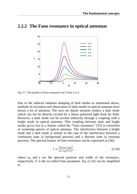
2.2.2 The Fano resonance in optical antennas
Fig. 2.7: The profiles of Fano resonances for F from 1 to 5.
Due to the reduced radiation damping of dark modes as mentioned above,
methods of excitation and observation of dark modes in optical antennas have
drawn a lot of attention. The zero net dipole moment renders a dark mode
which can not be directly excited by a linear polarized light from far field.
However, a dark mode can be excited indirectly through a coupling with a
bright mode in optical antennas. This coupling between dark and bright
modes gives rise to a feature called the “Fano resonance” [35] in extinction
or scattering spectra of optical antennas. The interference between a bright
mode and a dark mode is similar to the case of the interference between a
continuum state (a background process) and a discrete state (a resonant
process). The spectral feature of Fano resonance can be expressed as [36]:
𝐼 ≈(𝐹𝛾+𝜔−𝜔0)2
(𝜔−𝜔0)2+𝛾2 , (2.16)
where 𝜔0 and 𝛾 are the spectral position and width of the resonance,
respectively. F is the so-called Fano parameter. Eq. (2.16) can be simplified
to

Chapter 2
22
𝐼 ≈(𝐹+𝑞)2
𝑞2+1, (2.17)
where 𝑞 =𝜔−𝜔0
𝛾.
Fig. 2.7 shows the profiles of Fano resonance from Eq. (2.17) for
different values of F from 1 to 5. The constructive and destructive
interference between the continuum state and the discrete state changes the
Lorentzian resonance into an asymmetric profile.
The interference between a dark and a bright mode in an optical antenna
can be understood to be a Fano-like resonance. The relatively broader
spectral response of a bright mode is regarded as the continuum state. For a
dark mode which has narrower spectral response due to the reduced radiation
damping, it can be regarded as a discrete state. This interference between a
dark and a bright mode can be modelled by equations of a coupled oscillator
[37]:
��(𝑡) + 𝛾𝑏��(𝑡) + 𝜔𝑏2𝑝(𝑡) + 𝜅𝑞(𝑡) = 𝑔𝐸(𝑡) (2.18)
��(𝑡) + 𝛾𝑑��(𝑡) + 𝜔𝑑2𝑞(𝑡) + 𝜅𝑝(𝑡) = 0 (2.19)
p(t) and 𝑞(𝑡) are coordinate of the bright and dark mode, respectively. Eq.
(2.18) describes the equation of motion of the bright mode, which has a
damping factor 𝛾𝑏 and resonance frequency 𝜔𝑏 . The 𝑔𝐸(𝑡) is the external
force for the bright mode. Eq. (2.19) describes the equation of motion of the
dark mode, which has a damping factor 𝛾𝑑 and resonance frequency 𝜔𝑑. Two
oscillators are coupled with a coupling strength 𝜅. Eqs. (2.18), (2.19) can be
solved in the frequency domain by assuming the form 𝑝(𝑡) = 𝑝(𝜔)𝑒−𝑖𝜔𝑡 and
𝑞(𝑡) = ��(𝜔)𝑒−𝑖𝜔𝑡:
𝑝(𝜔) =𝐷𝑑(𝜔)𝑔��(𝜔)
𝐷𝑑(𝜔)𝐷𝑏(𝜔)−𝜅2 (2.20)
��(𝜔) =𝜅𝑔��(𝜔)
𝐷𝑑(𝜔)𝐷𝑏(𝜔)−𝜅2 , (2.21)

The fundamental concepts
23
Fig. 2.8: |��(𝜔)|2 profiles with (a) 𝜔𝑑 = 𝜔𝑏 + 0.1 s-1 (b) 𝜔𝑑 = 𝜔𝑏 − 0.1 (c) 𝜔𝑑 = 𝜔𝑏.

Chapter 2
24
where 𝐷𝑏(𝜔) = 1 − (𝜔
𝜔𝑏)2
− 𝑖𝛾𝑏(𝜔
𝜔𝑏2) , 𝐷𝑑(𝜔) = 1 − (
𝜔
𝜔𝑑)2
− 𝑖𝛾𝑑(𝜔
𝜔𝑑2) and
𝐸(𝑡) = ��(𝜔)𝑒−𝑖𝜔𝑡 . In the interference of a bright and a dark mode, the
damping factor for the bright mode 𝛾𝑏 is much larger than that of the dark
mode: 𝛾𝑏 ≫ 𝛾𝑑. Eqs. (2.20) - (2.21) can be also used as a classical model for
the phenomenon of electromagnetically induced transparency (EIT) [38].
Fig. 2.8 shows the profiles of |𝑝(𝜔)|2 with different 𝜔𝑑 as 𝜔𝑏 = 50 s-1
,
𝜅 = 6 s-2
, 𝛾𝑏 = 0.3 s-1
and 𝛾𝑑 = 0.02 s-1
. The dip in Fig. 2.8(a) - (c) comes
from the destructive interference between the bright and dark modes. For an
optical antenna, the dip in the extinction or scattering spectrum caused by the
destructive interference of a dark mode and a bright mode is called the
“Fano-dip”. This is illustrated further in Fig. 2.9, adapted from Ref. [39]. Fig.
2.9(a) shows the extinction spectrum of a gold heptamer. The Fano-dip
(marked D) comes from the destructive interference between a bright mode
shown in Fig. 2.9(b) and a dark mode shown in Fig. 2.9(c). The simulated
electric current in (b) and (c) are represented by blue arrows. The central gold
nanoparticle has an opposite direction of electric current with respect to that
of other gold nanoparticles, which reduces the net dipole moment of the dark
mode. The simulated near-field intensity are presented by the color scale. It is
obvious to see that the near-field intensity of dark mode shown in (c) is
higher than that of the bright mode shown in (b).
Fig. 2.9: (a) The extinction spectrum of a gold heptamer. The inset is the SEM picture of the heptamer. (b), (c) The simulated near-field intensity and corresponding electric currents (blue
arrows) at the spectral wavelengths marked C and D in (a). Figures are adapted from [39].

The fundamental concepts
25
Fig. 2.10: Measured extinction spectra for several gold nanoparticle periodic arrays. The particle
size is 123 nm×85 nm×35 nm. Inset (particle size 120 nm×90 nm×35 nm): When the diffraction edge is on the blue side of the main resonance, a much weaker effect is observed. <1, 0> and
<1,1> are diffraction direction for a periodic array. The figure is adapted from [40].
Besides the heptamer,the extinction spectrum of a periodic array of
metal particles also exhibit another type of Fano resonance—the surface
lattice resonance (SLR) [41, 42, 43, 44, 40, 45]. A SLR is a specific
collective mode of metal particles in a periodic array, which comes from the
intricate coupling of LSPR and in-plane diffracted waves. The SLR generates
a sharp spectral feature or a Fano-dip depending on the relative spectral
position of LSPR of monomers with respect to spectral position where in-
plane diffracted waves occur (or called “the Rayleigh condition”) [40].
Therefore, the SLR strongly depends on the size and shape of metal particles
(determining the spectral position of LSPR), and the pitch size of a periodic
metal particle arrays (determining the spectral position of in-plane diffracted
waves). Fig. 2.10 shows experimental spectra of a SLR in the extinction
spectra of periodic arrays of gold particles; adapted from Ref.[40]. We can

Chapter 2
26
find that sharp features of the SLR appear in extinction spectra when the in-
plane diffracted waves occur on the red side (the lower photon energy) of the
spectral position of the LSPR of a single gold particle, while a Fano-dip
appears when the in-plane diffracted waves occur on the blue side (the higher
photon energy) of the spectral position of the LSPR of a single gold particle.
In Chapter 6, we will discuss a SLR in a Sierpinski carpet optical
antenna. Different from the SLR in a periodic metal particle array measured
by the extinction spectra, we will visually show the SLR of the Sierpinski
carpet optical antenna by a back focal plane microscopy.

27
In contrast to the multi-crystalline gold films typically used as starting
material for the fabrication of optical antennas, here chemically-synthesized
single-crystalline gold flakes are employed. The recipe and procedure for
synthesizing single-crystalline gold flakes is introduced, as well as the
method of directly carving samples using focused ion beam (FIB) milling on
gold flakes. The results of fabricating gold nanostructures on both a thermal
evaporated multi-crystalline gold film and on a single-crystalline gold flake
are compared and discussed. The working principles and importance of the
various instrumentations used in the characterization of samples are
presented in the end of this chapter, including white light dark-field
microscopy, two-photon photoluminescence microscopy and back focal
plane microscopy.
Chapter 3
Sample fabrication and characterization
methodologies

Chapter 3
28
3.1 Fabrication of optical antennas
The performance of plasmonic nanostructures is greatly influenced by the
quality of metal materials. Multi-crystalline metal thin films (below 100 nm)
produced by thermal evaporation have been widely used in the fabrication of
plasmonic nanostructures. However, irregular granular boundaries are formed
in a metal thin film during the thermal evaporation process of metal onto a
glass substrate. These random-oriented grains (usually 30 – 50 nm diameter)
have different resistance to FIB milling, which causes unwanted features with
comparable grain sizes after the fabrication of plasmonic nanostructures.
These features introduce scattering, which reduces the lifetime of plasmons.
Recently, single crystalline gold flakes have been chemically
synthesized and applied for the fabrication of plasmonic nanostructures with
well-defined shapes [46]. In this section the synthesis of single-crystalline
gold flakes and the fabrication of fractal optical antennas on these flakes by
FIB milling are introduced.
3.1.1 Synthesis of single-crystalline gold flakes
Fig. 3.1: Single crystalline gold flakes and particles, dispersed in water solution.
The specific steps of synthesizing single-crystalline gold flakes follow the
procedure described in Ref. [47]. It begins with hydrogen tetrachloroaurate
(HAuCL4), dissolved in ethylene glycol. Poly (vinyl pyrrolidone) (PVP) is
then added as capping agent. The mixed solution is heated in an oil bath to
approximately 150 °C and after two hours the gold flakes appear in the
solution as shown in Fig. 3.1.

Sample fabrication and characterization methodologies
29
Fig. 3.2: The chemically-synthesized single crystalline gold flakes with some gold nanoparticles and nanowires on top of them, which are also formed during the synthesis process.
Fig. 3.3: A single-crystalline gold flake before (left) and after (right) the O2 plasma cleaning.
Most of contaminations on the surface of flake are removed after cleaning.

Chapter 3
30
Samples can be prepared by dropcasting the gold flakes and water
mixture onto the glass substrate and subsequently removing water drops by
clean and pressured nitrogen gas. Fig. 3.2 shows some gold flakes, gold
nanowires and nanoparticles on a glass substrate with a 100 nm thickness
conductive ITO layer. Also note that there are a few dark spots on gold flakes,
which is due to solvent residues from the manufacturing process.
3.1.2 Removing residual chemicals on a gold flake
by O2 plasma cleaning
The oxygen plasma cleaning process can be used to remove residual
contaminants (probably organic) remaining on a gold flake after the chemical
synthesis process. This cleaning step takes about 10 seconds. Fig. 3.3 shows
that most of contaminants have been removed after the O2 plasma cleaning.
This creates a uniform and smooth surface of the gold flake, which facilitates
the fabrication of our optical antennas.
3.1.3 Instrumentation
Fig. 3.4: (a) Photos of the FIB instrument. (b) View inside the vacuum chamber. (c) Schematic
representation of the dual-beam configuration.

Sample fabrication and characterization methodologies
31
To fabricate our samples, we used focused ion beam (FIB) milling (FEI Nova
600 dual beam) to carve nanostructures directly on single-crystalline gold
flakes. In the Fig. 3.4(a), two columns in the machine can be identified. The
FIB column is angled at 52 degrees relative to the vertical scanning electron
microscopy column. The sample stage can be moved with 5 degrees of
freedom for SEM imaging or FIB milling. Fig. 3.5 shows schematics of the
FIB and scanning electron microscopy columns. The Ga LMIS (liquid-metal
ion sources) consists of a tungsten needle with a heater to supply Ga to the tip.
Ga remains liquid after heating once. Ga is chosen for its durability (1500
hours) and stability (heating every 100 hours).
Fig. 3.5: The schematics of a FIB (left) and scanning electron microscopy column (right). LMIS:
liquid-metal ion source ; FEG: Field emission Gun. The image is adapted from [48].

Chapter 3
32
3.1.4 Fabrication result of the multi- crystalline
gold film and single-crystalline gold flakes
The advantages of using single-crystalline gold flakes for antenna fabrication
can be readily seen in Fig. 3.6. A single-crystalline gold flake (about 100 nm
thickness) is deposited above a thermal evaporated multi-crystalline gold film
(also about 100 nm thickness) as shown in the schematic on the lower right
of Fig. 3.6. The smooth and uniform surface of the single-crystalline gold
flake, compared to the multi-crystalline gold film, can be seen immediately.
We removed the gold layers by FIB milling to form a 5-by-5 µm square hole.
The residue of single-crystalline gold flake is a very thin film. However, for
the multi-crystalline gold film, it ends in blobs of gold, which are the result
of irregular crystal grains in it. The roughness of residuals of the multi-
crystalline gold is much higher than that of the single-crystalline gold flake.
This shows the superiority of single-crystalline gold flakes for the fabrication
of plasmonic nanostructures.
Fig. 3.7(a) shows the fabrication with single-pass milling of a gold cross
bar antenna on a multi-crystalline gold film. Panel (b) shows the result of
single-pass milling on a single-crystalline gold flake, while (c) shows the
fabrication result on a single-crystalline gold flake with multi-pass milling
(15 passes) and software drift correction applied. The samples shown in (a)
and (b) were both fabricated with single-pass FIB milling; in both residual
gold nanoparticles can be seen. The difference is that the residual particle
size for the single-crystalline gold flake is much smaller than that of the
multi-crystalline gold film. This is because of the larger and irregular crystal
grains in the multi-crystalline gold film. We notice that, in (a) and (b), the
horizontal bars are wider than vertical ones. This is due to the redeposition of
gold particles. During FIB milling process, the ion beam raster-scanned from
upper-left to lower-right. This causes the redeposition of removed gold
nanoparticles near the lower edges of the horizontal bars. In (c) we can see
that the shape of cross bar antenna is well-defined and the background is
clean. Therefore, we chose the single-crystalline gold flake and multi-pass
FIB milling in combination of position feedback to fabricate our optical
antennas.

Sample fabrication and characterization methodologies
33
Fig. 3.6: The fabrication result of a single-crystalline gold flake on the top of a multi-crystalline
gold thin film.
Fig. 3.7: (a) A cross bar nanoantenna fabricated by single-pass FIB milling on a multicrystalline gold film with thickness of 40 nm. Panels (b) and (c) show cross bar nanoantennas fabricated on
a single-crystalline gold flake with single-pass and multi-pass (15 passes) milling, respectively.

Chapter 3
34
Fig. 3.8: A Sierpinski carpet optical antenna fabricated on a single-crystalline gold flake by FIB
milling.
Fig. 3.8 shows an example of the fabrication of a Sierpinski carpet
optical antenna on a single-crystalline gold flake by FIB milling (30 pass).
The flake was pre-thinned to a thickness of ~40 nm. In FIB milling process,
the acceleration voltage was 30 kV and the Ga-ion current was 1.5 pA. The
monomer size is 80 ± 8 nm (diameter) and 40 ± 5 nm (thickness); the gap
distance between monomers is 30 ± 11 nm. We can see that the shape of
monomers is uniform and the background is clean without residuals of gold
nanoparticles. We will discuss the Sierpinski carpet optical antenna in detail
in following chapters.
3.2 Instrumentation
In this section, I will introduce the instrumentations and techniques used in
experimental works of this thesis: the white light dark-field microscopy used
for the determination of the resonant wavelength, the two photon
photoluminescence for the measurement of the near-field intensity and the
back focal plane microscopy for the visualization and quantification of the
intensity of plasmonic modes of optical antennas. These measurements are
critical in the design and application of optical antennas.

Sample fabrication and characterization methodologies
35
3.2.1 White light dark-field microscopy
Fig. 3.9: The schematic of white light dark field microscopy. Note the inclusion of a beam block
for annular illumination.
In optical microscopy, dark-field describes an illumination technique used to
enhance the contrast in unstained samples. It works by illuminating the
sample with light that will not be collected by the objective lens, and thus
will not form part of the image. This produces the classic appearance of a
dark background with bright objects on it [49].
The white light dark-field microscope, utilizing the dark-field
illumination configuration, has become a widely-utilized tool in plasmonics
research area to determine the resonant wavelength of gold nanostructures
[50] [51] [52] [53]. In this technique, an incident beam illuminates the
sample of interest, and scattered light from the metal nanostructure is
collected by an objective and sent into a spectrometer. The stray light from
the substrate is not collected by the objective to minimize background noise.
A pinhole before the spectrometer entrance can be used in a confocal like
design to ensure that scattered light from only a single nanostructure enters
the spectrometer.

Chapter 3
36
Fig. 3.10: The scattering spectrum of a gold nanoparticle with 100 nm diameter. The green curve is the experimental data measured by the white light dark-field microscope shown in Fig. 3.9.
The red curve is the finite-difference time-domain (CST MWS 2013) simulation result. The
more broad and red shift of the experimental result compared with the simulation result come from the glass substrate which is not considered in the simulation.
Our home-built dark-field spectrometer setup [1] is shown schematically
in Fig. 3.9. White light from a Xenon Arc lamp (Oriel 71213, Newport) is
sent into a microscope (IX71, Olympus) and focused onto samples with a 1.4
N.A. oil-immersion objective (UPLSAPO 100XO, Olympus). To obtain a
dark-field illumination, the central part of the light beam is blocked. The
scattered light is collected with a 0.3 N.A. objective (UPLFLN 10X2,
Olympus), and subsequently focused onto a 50 µm diameter pinhole before
the spectrometer (AvaSpec-3648-USB2, Avantes). The effective area on the
sample plane from which light was collected was estimated to be a 5 µm
diameter circle, hence completely encompassing the full nanostructure.
Spectra were typically acquired in 5 seconds to allow the detector to
accumulate enough signal. The scattering spectra are normalized by dividing
the scattered light spectrum to the system response retrieved by removing the
beam block (bright field illumination) to get rid of the inherent wavelength
dependence of the white light source.

Sample fabrication and characterization methodologies
37
Fig. 3.10 shows an example of dark-field scattering spectrum of a gold
nanoparticle with 100 nm diameter measured by the white light dark-field
microscope shown in Fig. 3.9. The measured resonance frequency (570 nm)
has a red shift compared with simulated one (530 nm) due to the ignorance of
the effect of glass substrate in the finite-difference time-domain (CST MWS
2013) simulation.
3.2.2 Two-Photon Photoluminescence (TPPL)
Microscopy
Fig. 3.11: The schematic of two photon photoluminescence (TPPL) microscopy.
In the plasmonics research field, two-photon photoluminescence (TPPL) has
been widely used for mapping hot spots of gold nanostructures spatially and
spectrally [55], as well as the measurement of intensity enhancement of gold
bowtie optical antennas [56]. Recently TPPL was used to reveal the surface
plasmon local density of states in thin single-crystalline triangular gold
nanoprisms [57]. When focusing a near-infrared intense pulsed laser beam on
gold, electrons in the valence d band absorb two photons for the transition to
the conduction sp band. In this process, which is still actively studied,
intraband transitions in the sp band can play a role [58]. The sensitivity of
TPPL to the high electric field enhancements that occur locally in gold

Chapter 3
38
nanostructures is generally attributed to its absorption of multiple photons
which will be nonlinearly dependent on pump power. We use TPPL
microscopy to estimate the near-field intensity enhancements of our gold
nanostructures. The schematic of our TPPL microscopy is shown in Fig. 3.11.
Fig. 3.12: (a) TPPL image of gold nanoparticle clusters. (b) the TPPL spectrum. The sharp cut-
off around 680 nm is caused by the short-pass filter.
To perform TPPL confocal microscopy, we used a mode-locked laser
(Micra, Coherent Inc.) with a tunable wavelength from 750 to 830 nm. A
pulse duration is around several hundred femto-seconds. The beam is sent
into an inverted microscope (IX71, Olympus), and directed by a dichroic
mirror (700nm dichroic short-pass filter, Edmund Optics) into the objective
(UPLSAPO 100XO, Olympus). Samples are placed on a piezo scanning
stage and moved relative to the focused excitation beam spot. The generated
TPPL is collected by the same objective used for focusing the excitation
beam, and 2nd
short pass filtered (FF01-694/SP, SEMROCK) is used to reject
the excitation light. We thus only collect the visible wavelength contribution
of the TPPL. The luminescent signal is focused onto a pinhole before a
single-photon counting avalanche photodiode (Perkin-Elmer).
Fig. 3.12(a) shows the TPPL image of gold particles clusters with dia-
meters around 100 nm. The brighter spots show the higher near field intensity.
Panel (b) shows the spectrum of TPPL measured by a spectrometer
(AvaSpec-3648-USB2, Avantes). The broadband TPPL with a visible
wavelength range of 450 ~ 680 nm is the result of the absorption of two near-

Sample fabrication and characterization methodologies
39
Fig. 3.13: (a) the TPPL counts v.s. excitation laser power. (b) the logarithmic plot of TPPL counts v.s. excitation laser power.
infrared photons by an electron in the valence d band of gold, then the
electron is excited to the conduction band, which creates a hole in the d band.
The radiative recom-bination of the hole in the d band and electrons in the
conduction band renders the TPPL [58].
To confirm that the luminescence signals we retrieved in Fig. 3.12(b)
are indeed the result of two-photon absorption of the metal nanoparticle
cluster (the nonlinear property of TPPL), we measure the relation of
luminescence counts of the gold nanoparticle cluster with respect to the
excitation laser power as shown in Fig. 3.13(a). The logarithmic plot of this
relation is shown in Fig. 3.13(b); the red line is the linear fit of the
logarithmic plot, showing the slope 1.9, which is close to the slope 2 given by
the quadratic relation: TPPL ~ I2 or log(TPPL) ~ 2log(I), and I is the laser
intensity on the gold nanoparticle cluster. Therefore, the signals retrieved in
our microscopy can be confirmed to be TPPL.
3.2.3 Back focal plane (leakage radiation)
microscopy
An important characteristic of SPP modes is that their spatial extent is
determined by the shape of metal nanostructures rather than by the optical
wavelength. The instruments for the observation of SPP mode consequently

Chapter 3
40
adapted essentially to the subwavelength regime and being capable of
imaging the propagation of SPPs. Usually the analysis of the subwavelength
regime requires near-field scanning fiber tip [59] to frustrate and collect the
evanescent components of the electromagnetic fields associated with SPPs.
However, when the metal film on which nanostructures are built is thin
enough (80-100 nm) and when the refractive index of substratum medium
(usually glass) is higher than the one of the superstratum medium (air),
another possibility for analyzing SPP propagation occurs. This possibility is
based on the detection of coherent leaking of SPPs through the substratum.
Such a far-field optical method is called back focal plane or leakage radiation
microscopy [24] [25] [26] and allows a direct and quantitative imaging of
SPP propagation on thin metal films. However, in our works, we use the back
focal plane microscopy on the sample formed by gold nanoparticles rather
than gold films.
Fig. 3.14: The schematic of the back focal plane microscopy. BFP: back focal plane; BB: beam
blocker; OP: object plane. The red beams represent the diffraction light from the BFP, the green
beam represents the light from the OP. The zero order diffracted light and incident light are blocked by the BB.
Fig. 3.14 shows the schematic of our home-built back focal plane
microscope. The photon energy of the excitation light source can be tuned
from 1.3 to 2.25 eV (550 to 950 nm) with a spectral bandwidth around 2 nm
by feeding the broadband white light source (Fianium SC400-4) into the
mono-chromator (Acton SP2100-i). The excitation light is focused by a 0.3
N.A. objective (UPLFLN 10X2, Olympus) and the beam spot size is adjusted

Sample fabrication and characterization methodologies
41
Fig. 3.15: (a), (b) diffraction pattern of a Sierpinski carpet optical antenna with an incident plane
wave at x-direction. The red double arrow is the direction of polarizer, and green double arrow is the direction of the analyzer. The red and green circles correspond to the wave vector of the light
line in air and in the glass substrate, respectively.
to cover the whole sample. The diffracted light is collected by a 1.4 N.A. oil-
immersion objective (UPLSAPO 100XO, Olympus). The image at the back
focal plane (BFP) is relayed by lenses I, II and III in Fig. 3.14 onto the CCD
(red rays). A beam block (BB) is used for blocking the incident light. With
lenses I, II and IV, we can alternatively relay the image at the object plane
(OP) onto the CCD (light green ray). With the polarizer and analyzer (GT10,
Thorlabs) shown in Fig. 3.14, we can choose the BFP image with x and y
polarization.
Fig. 3.15 shows an example of the diffraction pattern of our sample – a
Sierpinski carpet optical antenna – on the back focal plane of our back focal
plane microscope. The red and green circles correspond to the wave vectors
of the light line in air and the glass substrate, respectively. Spots appearing
between the red and green circles correspond to the evanescent waves in air
but propagative waves in the glass substrate. This is a very important
property of observing the near-field plasmonic mode by BFP microscopy,
which will be further explained in Chapter 6.

42

43
In this chapter we analyze the dipole moment structure of out-of-plane and
in-plane eigenmodes of Sierpinski carpet optical antennas, and calculate
Fourier spectra and far field radiation patterns of eigenmodes to identify their
super- or sub-radiance properties. These analyses help us to understand the
features of eigenmodes from using the self-similarity principle to construct
optical antennas. Furthermore, the eigen-decomposition method introduced
here will also be used in Chapter 6 to explain the specific subradiant
resonance observed by back focal plane microscopy.
Chapter 4
Analysis of eigenmodes by eigen-decomposition
method

Chapter 4
44
4.1 The eigen-decomposition theory of plasmonic
resonances
The analysis of the electromagnetic resonance of metallic nanostructures can
be quite complicated because of the geometric complexity. For fractal optical
antennas, this complexity comes from the self-similarity in the arrangement
of metal nanoparticles. To understand the influence of self-similarity on the
electromagnetic resonance of fractal antennas, we calculate the plasmonic
eigenmodes of 0th
- 3rd
order Sierpinski carpet optical antennas according to
the eigen-decomposition method [60] [61]. The eigen-decomposition method
is based on the dipolar coupling between metal nano-particles, and was first
used by Markel et al [60].
4.1.1 The coupled dipole equation
The eigenmodes are the key to understand the collective electromagnetic
resonances of metal nanoparticles. Under the coupled dipole approximation,
each metal nanoparticle is assigned an electric dipole moment. With the
existence of an external driving electric field 𝐸𝑒𝑥𝑡,𝑚 = 𝐸𝑚𝑒−𝑖𝜔𝑡 acting on the
mth
particle in a metal nanoparticle (MNP) cluster, the coupled dipole
equation is [62] [63]:
𝑃𝑚 = 𝛼[𝐸𝑒𝑥𝑡,𝑚 + ∑ 𝐴𝑚,𝑛𝑃𝑛𝑛≠𝑚 ] , (4.1)
where 𝑃𝑚 is the dipole moment of mth
MNP, Am,n is the tensor that represents
the interaction matrix between a receiving dipole at 𝑟 𝑚 and a radiating dipole
at 𝑟 𝑛. Am,n is defined as:
𝐴𝑚,𝑛(𝑟 ≡ (𝑟 𝑚−𝑟 𝑛)) = 𝑘03 [𝐵(𝑘0|𝑟 |)𝛿𝑖𝑗 + 𝐶(𝑘0|𝑟 |)
𝑟𝑖𝑟𝑗
|𝑟 |2] (4.2)
𝐴𝑚,𝑛(𝑟 ≡ (𝑟 𝑚−𝑟 𝑛)) = 𝑘03 [𝐵(𝑘0|𝑟 |)𝛿𝑖𝑗 + 𝐶(𝑘0|𝑟 |)
𝑟𝑖𝑟𝑗
|𝑟 |2] (4.3)
𝐶(𝑥) = (−𝑥−1 − 3𝑖𝑥−2 + 3𝑥−3)𝑒𝑖𝑥 , (4.4)
where k0=ω/ch, ch is the speed of light in the background medium and here
we set the medium as air, and i, j=1, 2, 3 are component indices of r in

Analysis of eigenmodes by eigen-decomposition method
45
Cartesian coordinates. The term 𝑒−𝑖𝜔𝑡 is omitted in Eq. (4.1). If we define
Am,m=1/α, Eq. (4.1) can be written as:
𝐸𝑒𝑥𝑡,𝑚 = 𝐴𝑚,𝑚𝑃𝑚 + ∑ 𝐴𝑚,𝑛𝑃𝑛𝑛≠𝑚 (4.5)
This equation can be further combined to be:
∑ 𝐴𝑚,𝑛𝑃𝑚 =𝑁𝑛=1 𝐸𝑒𝑥𝑡,𝑚 , (4.6)
where Am,n is the 3 by 3 matrix defined by Eqs. (4.2), (4.3) and (4.4) and N is
the number of MNPs in a cluster. The polarizability α here is the dynamic
dipole polarizability :
𝛼(𝜔) = 𝑖3𝑐ℎ
3
2𝜔3 𝑎1(𝜔) , (4.7)
where
𝑎1(𝜔) =𝜀(𝜔)𝐽1(𝑘𝑠𝑟)𝜕𝑟[𝑟𝐽1(𝑘0𝑟)]−𝜀ℎ𝐽(𝑘0𝑟)𝜕𝑟[𝑟𝐽1(𝑘𝑠𝑟)]
𝜀(𝜔)𝐽1(𝑘𝑠𝑟)𝜕𝑟[𝑟𝐻1(1)
(𝑘0𝑟)]−𝜀ℎ𝐻1(1)
(𝑘0𝑟)𝜕𝑟[𝑟𝐽1(𝑘𝑠𝑟)]|𝑟=𝑟0
. (4.8)
J1(x) is the spherical Bessel function of the first kind, H1(1)
(x) is the spherical
Bessel function of the third kind (or spherical Hankel function of the first
kind), and ks=ω√ε(ω)/ch. Different from Eq. (2.15), the dynamic dipole
polarizability (Eq. (4.7) and (4.8)) proposed by Doyle [64] includes the effect
of radiation loss and absorption loss. Therefore it provides more accurate
results for metal nanoparticles.
4.1.2 The concept of eigenpolarizability
We can express Eq. (4.6) as
𝐴�� = 𝐸𝑒𝑥𝑡 . (4.9)
To analyze the resonances of a cluster MNP, we consider the following
eigenvalue problem [60]:
𝐴�� = 𝜆�� , (4.10)

Chapter 4
46
where λ and �� = (… , 𝑝𝑚−1, 𝑝𝑚, 𝑝𝑚+1, … )𝑇are the complex eigenvalues and
eigenvectors of the interaction matrix A. The eigen-polarizability is defined
as [61]:
𝛼𝑒𝑖𝑔 ≡1
𝜆 (4.11)
which can be interpreted as the collective response function of the MNP
cluster under the external electric field pattern proportional to the
corresponding eigenvector �� . There are 3N eigenmodes for a MNP cluster.
For a 2D MNP cluster in a plane, we can further decompose the 3N×3N
interaction matrix A into an N×N out-of-plane (px, py = 0, pz ≠ 0) and a 2N
×2N in-plane (px,py ≠ 0, pz = 0) sub-matrix. The eigenvector P gives the
spatial distribution of the plasmonic eigenmode in a MNP cluster, while αeig gives the response of this plasmonic eigenmode to the excitation wavelength.
In this work we use silver nanoparticles as monomers in the Sierpinski
carpet optical antenna of all orders. The dielectric function of silver is
adopted from the experimental data [22]. The interaction matrix A is a
symmetric complex matrix, therefore, its eigenvectors form a complete set
but are not orthogonal to each other set [60]. We can decompose a plamonic
mode that is excited by any type of excitation beam, such as a plane wave, in
a MNP cluster as a combination of eigenmodes calculated by the eigen-
decomposition theory.
4.1.3 Localization of plasmonic eigenmode
The eigenvector �� retrieved from solving the eigenvalues of interaction
matrix A in Eq. (4.6) gives the spatial distribution of plasmonic eigenmode.
The participation ratio (PR) of the nth
eigenmode is defined as [65] [66]:
𝑃𝑅(𝑛) =1
𝑁
(∑ |𝑝𝑚(𝑛)
|2
𝑁𝑚=1 )
2
(∑ |𝑝𝑚(𝑛)
|4
𝑁𝑚=1 )
, (4.12)
which can be used as an indicator of the spatial localization properties of the
nth
eigenmode. In the case of PR = 1, the spatial extension of this eigenmode
is equal in all MNPs in the system. If PR = 1/N, this eigenmode is completely
localized to single MNP. In general, an eigenmode can be regarded as

Analysis of eigenmodes by eigen-decomposition method
47
localized as its PR << 1. Note that N in Eq. (4.12) is equal to 1, 8, 64, and
512 for the 0th
, 1st, 2
nd, and 3
rd order Sierpinski carpet optical antennas,
respectively.
4.2 Out-of-plane eigenmodes
In this section we analyze the out-of-plane eigenmodes (px, py = 0, pz ≠ 0)
of 0th
– 3rd
order Sierpinski carpet optical antennas by the eigen-
decomposition method.
4.2.1 The eigenpolarizability spectra of out-of-
plane eigenmodes
For periodic MNP arrays, the super- or sub-radiance property of plasmonic
eigenmodes can be recognized by the dispersion relation. If the Bloch wave
vector k of an eigenmode of periodic arrays is smaller than that of the
incident light, this eigenmode can couple easily with the incident light, and
consequently has a higher radiation loss, therefore, this eigenmode is
recognized as ‘super-radiant’ or ‘bright’. If the Bloch wave vector k of an
eigenmode larger than that of the incident light, this eigenmode can hardly
couple with the incident light, and consequently has lower radiation loss.
This eigenmode is recognized as ‘sub-radiant’ or ‘dark’. The sub- and super-
radiance property have been discussed in Chapter 2. However, for aperiodic
arrays such as the Sierpinski carpet optical antenna, due to the absence of
translational invariance, there does not exist a Bloch wave vector as for the
periodic arrays. The super- or sub-radiance of an eigenmode is recognized by
its Fourier amplitude spectrum. If the magnitude of most k vectors of an
eigenmode is smaller than the magnitude of the incident light, we can
recognize this eigenmode is superradiant for it can be coupled with the
incident light. On the other hand, if the magnitude of most k vectors of an
eigenmode is larger than the magnitude of the incident light, it is subradiant.
Fig. 4.1 shows the calculated imaginary part of αeig/r03 of the Sierpinski
carpet optical antenna up to the 3rd
order. The energy extinction of a MNP
cluster by the external field is given by [61]
𝑃𝑙𝑜𝑠𝑠 = 𝜔𝐼𝑚(𝛼𝑒𝑖𝑔)∑ 𝐸𝑒𝑥𝑡,𝑚𝑚 . (4.13)

Chapter 4
48
Since the power loss of the system is proportion to Im(αeig) in Eq. (4.13), the
spectral position of the peak of Im(αeig/r03), similar to the polarizability α of a
single MNP, indicates the resonant frequency of that eigenmode of the MNP
system.
Fig. 4.1: (a) - (d) are the eigen-polarizability spectra of the out-of-plane eigenmode of 0th - 3rd order Sierpinski carpet optical antenna, respectively.
Fig. 4.1(a) shows the Im(αeig/r03) of the monomer of Sierpinski carpet
optical antenna, which indicates the resonance of a single silver nanoparticle
at wavelength 380 nm. We can easily connect all data points in Fig. 4.1(a) to
have an eigen-polarizability spectrum curve of a monomer. When the
monomer number increases in 1st - 3
rd order Sierpinski carpet optical antenna,
the connection of data points in Fig. 4.1(b) - (d) becomes impossible due to
the eigenvalue retrieving process in MATLAB (MathWorks). Fig. 4.2 shows
the normalized far field radiation pattern |Eff|2 of the eigenmode in Fig. 4.1(a)

Analysis of eigenmodes by eigen-decomposition method
49
on a unit sphere representing all the scattering directions. Eff is calculated by
[60]
𝐸𝑓𝑓 = 𝑘2 𝑒𝑖𝑘𝑅
𝑅∑ [𝑃𝑗 − (𝑠 ∙ 𝑃𝑗)𝑠]𝑒
−𝑖𝑘𝑠∙𝑟𝑗𝑁𝑗=1 , (4.14)
where rj is the position of a MNP, s is the unit vector in the scattering
direction and R is the distance from the center of mass of a MNP to the
detector with 𝑅 ≫ |𝑟𝑖 − 𝑟𝑗| and 𝑘𝑅 ≫ 1. Fig. 4.2 shows actually the far field
radiation pattern of a single dipole located in the origin of coordinate and
pointing at the z direction.
Fig. 4.2: Far field radiation pattern of the eigenmode shown in Fig. 4.1(a) at peak wavelength 380 nm.
Fig. 4.1(b) shows the Im(αeig/r03) of 1
st order of Sierpinski carpet optical
antenna. For the eight MNPs in this structure there should be 24 curves
representing 24 plasmonic modes : 8 out-of plane and 16 in-plane. In Fig.
4.1(b) we only find 6 curves, which indicates there are two degenerate modes.

Chapter 4
50
4.2.2 The eigenmodes of superradiant peak
Fig. 4.3: (a) - (c) are the real part of dipole moment of eigenmodes at peaks of 355 nm in Fig.
4.1(b) - (d), respectively. The red color represents the z direction. (d) - (f) are Fourier amplitude spectra and (g) - (i) are far field radiation patterns of eigenmodes shown in (a) - (c), respectively.
Note that the far field radiation patterns are normalized. The red circle in (d) – (f) represents the
magnitude of the wave vector of incident light.
We notice that there are two major peaks in Fig. 4.1(b) - (d) with positions at
355 and 390 nm, respectively. Fig. 4.3(a) - (c) show the real parts of the
dipole moment of eigenmodes with maximum value of Im(αeig/r03) (at around

Analysis of eigenmodes by eigen-decomposition method
51
355 nm) in Fig. 4.1(b) - (d), respectively. We find that all dipole moments of
monomers are pointing in the same direction, and we can easily identify that
these three eigenmodes are superradiant. To get more understanding on the
superradiance property of these eigenmodes, we calculate their Fourier
amplitude spectra of dipole moment by the formula
|𝑃��(𝑘𝑥 , 𝑘𝑦)| = | ∫ 𝑃𝑧(𝑥, 𝑦)𝑒−𝑖(𝑘𝑥𝑥+𝑘𝑦𝑦)𝑑𝑥𝑑𝑦 | . (4.15)
Fig. 4.3(d) - (f) show the Fourier amplitude of the dipole moment of
eigenmodes shown in Fig. 4.3(a) - (c), respectively. The superradiance of
three eigenmodes can be easily identified: most of wave vectors are within
the red circle, which represents the wave vector of incident light. Fig. 4.3(g) -
(i) are far field radiation patterns calculated by Eq. (4.14). As the order of
Sierpinski carpet optical antenna increases, the Fourier spectra and far field
radiation patterns of these three eigenmodes become more structured. The PR
values of the eigenmodes shown in Fig. 4.3(a) - (c) are 0.8, 0.83 and 0.49,
respectively. As the order of Sierpinski carpet optical antenna increases, the
eigenmodes in the sub-radiant peak get more localized, and the dipole
moment distributions of higher order Sierpinski carpet optical antenna in Fig.
4.3(b) and (c) have similar features with the 1st order eigenmode shown in
Fig. 4.3(a): the four corners have weaker dipole moments and a point
symmetry with respect to the center of the Sierpinski carpet optical antenna.
4.2.3 The eigenmodes of subradiant peak
Fig. 4.4(a) - (c) show the real part of the dipole moment of eigenmodes with
maximum Im(αeig/r03) (at 391 nm) in Fig. 4.1(b) - (d), respectively, and Fig.
4.4(d) - (f) are their Fourier amplitude spectra of the dipole moment
calculated by Eq. (4.15), and Fig. 4.4(g) - (i) are their far field radiation
patterns calculated by Eq. (4.14). Fig. 4.4 (a) shows two degenerate
eigenmodes. Different from the eigenmodes in the superradiance peak shown
in Fig.4.3(a) - (c), eigenmodes in Fig. 4.4(b) and (c) have a symmetry on
anti-phased dipoles (blue and red squares): the dipole moments on their
diagonal lines and x, y-axis lines are zero (white squares), and anti-phase
dipoles are symmetric with respect to these four lines, too. Due to the highly
symmetric anti-phase dipoles in these eigenmodes, the radiation damping is
reduced and consequently these eigenmodes possess a higher quality factor
compared with superradiant eigenmodes shown in Fig. 4.3(a) - (c). From

Chapter 4
52
their Fourier spectra in Fig. 4.4(d) - (f), we can see that as the order of the
Sierpinski carpet optical antenna increases, the spectra become more
structured but still distribute in the same areas outside of the red circle. Fig.
4.4(g) - (i) show that far field radiation patterns are also getting more
structured. Contrary to the superradiant eigenmodes discussed in Fig. 4, we
call this peak the ‘subradiant peak’. The PR value for three eigenmodes
shown in Fig. 4.4(a) - (c) are 0.68, 0.58 and 0.47, respectively, which shows,
similar to superradiant eigenmodes shown in Fig. 4.3(a) - (c), eigenmodes get
more localized as the order increases.

Analysis of eigenmodes by eigen-decomposition method
53
Fig. 4.4: (a) - (c) are the real part of dipole moment of eigenmodes at peaks of 391 nm in Fig. 4.1(b) - (d), respectively. The red and blue color represent the z and –z direction. (d) - (f) are
Fourier amplitude spectra and (g) - (i) are far field radiation patterns of (a) - (c), respectively.
The red circle in (d) - (f) represents the magnitude of the wave vector of incident light.

Chapter 4
54
4.3 In-plane eigenmodes
In this section we analyze the in-plane eigenmodes (px, py ≠ 0, pz = 0) of 0th - 3
rd
order Sierpinski carpet optical antennas by the eigen-decomposition method.
4.3.1 The eigenpolaribility spectra of in-plane
eigenmodes
Fig. 4.5(a) - (d) show the calculated Im(αeig/r03) of in-plane (px and py ≠ 0, pz
= 0) eigenmodes of 0th
- 3rd
order Sierpinski carpet optical antennas. Fig.
4.5(a) is a degenerate curve which is exactly the same as the curve shown in
Fig. 4.1(a). Fig. 4.6(a) and (b) show the far field radiation patterns of these
two degenerate eigenmodes in Fig. 4.5(a) and are exactly the far field
radiation patterns of a single dipole pointing in x and y direction, respectively.
Due to the degeneracy in eigenmodes, Fig. 4.5(b) shows only 12
different curves representing 16 (4 degenerate eigenmodes) in-plane
plasmonic eigenmodes. Contrary to the eigenpolarizability spectra shown in
Fig. 4.1, we find that as the order increases, many new peaks arise, while the
peaks at 364 and 385 nm in Fig. 4.5(b) - (d) remain at the same position. Fig.
4.7 is the vector plot of the real part of the dipole moment (px, py) of the in-
plane plasmonic eigenmode, (a) - (c) show the eigenmodes of 1st - 3
rd order
Sierpinski carpet optical antenna with maximum Im(αeig/r03) value at 385 nm,
respectively.

Analysis of eigenmodes by eigen-decomposition method
55
Fig. 4.5: (a) - (d) are the eigenpolarizability spectra of the in-plane eigenmode of 0th - 3rd order
Sierpinski carpet optical antenna, respectively.
Fig. 4.6: (a), (b) are the far field radiation patterns of two degenerate modes in Fig.4.5(a).

Chapter 4
56
4.3.2 The self-similarity in the structure of dipole
moment
In Fig. 4.7(a), we find that the anti-phase dipole moments have point
symmetry with respect to the center of the 1st order Sierpinski carpet optical
antenna. Fig. 4.7(d) and (g) are Fourier spectra of the dipole moment of the
eigenmode calculated by Eq. (15) with Pz(x,y) replaced by Px(x,y) and Py(x,y),
respectively. Most wave vectors of the eigenmode are outside of the circle of
light line, showing its subradiance property. Fig. 4.7(j) shows the far field
radiation pattern calculated by Eq. (4.14).
Fig. 4.7(b) and (c) are vector plots of the real part of the dipole moment
(px, py) of eigenmodes with maximum Im(αeig/r03) at 385 nm in Fig. 4.5(c)
and (d), respectively. From the vector plots we find that the dipole moment
structures of these eigenmodes also possess self-similarity. In Fig. 4.7(b), the
vector plot shows that 1st order subunits have a similar dipole moment
structure as the 1st order shown in Fig. 4.7(a): the anti-phase dipole moment
has a point symmetry with respect to the center of each 1st order subunit. Fig.
4.7(c) also shows similar dipole moment structures in its 1st order subunits. In
Fig. 4.7(a) - (c), all eigenmodes have a point symmetry of the anti-phase
dipole moment with respect to the center, which reduces of radiation
damping as the order increases. As the order increases from 2nd
to 3rd
, we find
the dipole moment concentrate more on some parts of monomers, which
means eigenmodes getting more localized as the order increases. The
calculated PR value of these three eigenmodes are 0.97, 0.62 and 0.23,
respectively. From the Fourier spectra of px and py in Fig. 4.7(d) - (f) and (g) -
(i), we notice that wave vectors distribute in the same k space region and
become more structured and discretized as the order increases.
Fig. 4.8(a) - (c) are the vector plots of the real part of dipole moment of
the in-plane eigenmode which has maximum Im(αeig/r03) value at 364 nm in
Fig. 4.5(b) - (d), respectively. In Fig. 4.8(b) and (c), we see that the dipole
moment structure of the 1st order subunits have the same symmetry as the
dipole moment structure of 1st order Sierpinski carpet optical antenna shown
in Fig. 4.8(a), in which the anti-phase dipole moment is symmetric with
respect to the center, which reduces the radiation loss. We can see that, in Fig.
4.8(c), the dipole moments distribute in inner and outer 1st order subunits,
which shows more localized property as the order increases. The PR value of

Analysis of eigenmodes by eigen-decomposition method
57
eigenmodes shown in Fig. 4.8(a) - (c) are 0.94, 0.8 and 0.62, respectively.
From Fig. 4.8(d) - (f), as the eigenmodes shown in Fig. 4.7(a) - (c), most of
their wave vectors are smaller than that of the incident light which is
represented by the red circle. It shows their sub-radiance property. With the
increase of order, the Fourier spectra (d) - (i) and far field radiation patterns (j)
- (l) become more structured.

Chapter 4
58
Fig. 4.7: (a) - (c) are the real parts of the dipole moment of eigenmodes at the peak 385 nm in
Fig. 4.6(b) - (d), respectively. (d) - (f) are the Fourier spectra of dipole moment px and (g) - (i) are the Fourier spectra of dipole moment py of eigenmodes in (a) - (c), respectively. And (j) - (l)
are the far field radiation patterns of (a) - (c), respectively.

Analysis of eigenmodes by eigen-decomposition method
59
Fig. 4.8: (a) - (c) are the real part of dipole moment of eigenmode at peak of 364 nm in Fig. 4.6
(b) - (d), respectively. (d) - (f) are the Fourier spectra of dipole moment px and (g) - (i) are the Fourier spectra of dipole moment py of eigenmodes in (a) - (c), respectively. And (j) - (l) are the
far field radiation patterns of eigenmodes shown in (a) - (c), respectively.

Chapter 4
60
4.4 The trajectory plot of wavelength - far field
radiation energy - PR value
Fig. 4.9: (a) - (c) show the trajectory plot of [wavelength (every 10 nm), radiation energy
(normalized), PR] for out-of-plane eigenmodes of 1st - 3rd order Sierpisnki carpet optical antenna.
(d) - (f) are the trajectory plot for the in-plane eigenmodes.
Fig. 4.9(a) - (c) show trajectory plots of wavelength, radiation energy
(normalized), and PR of the out-of-plane eigenmodes for the 1st - 3
rd order

Analysis of eigenmodes by eigen-decomposition method
61
Sierpinski carpet optical antennas. Similarly, Fig. 4.9(d) - (f) show the
trajectory plots for the in-plane eigenmodes. The normalized far field
radiation energy can indicate the sub- or super-radiance of eigenmodes.
When PR ~ 1, it is a superraidant eigenmod e; while PR ~ 0 indicates the
eigenmode is subradiant. The trajectory map in Fig. 4.9 gives us statistical
information on the sub- and super-radiance of eigenmodes with respect to the
wavelength and PR value. The PR value indicates the level of localization of
an eigenmode. In Fig. 4.9, we find that eigenmodes possess lower PR value
as the order increases, which means higher order Sierpinski carpet optical
antennas can have stronger localized eigenmodes.
Fig. 4.10: (a) the projection of [Radiation energy, PR] of Fig. 4.9(c). (b) the projection of
[Radiation energy, PR] of Fig. 4.9(f).
From Fig. 4.9(a), (b), it can be seen that the PR value of some curves
changes with the wavelength. This shows that the dipole moment structure
may change with resonance on or off. Further, it is can be seen that most of
the eigenmodes are subradiant, as most of the points in the trajectory plots
have normalized radiation energy ~ 0. For 3rd
order structures in panels (c)
and (f), this situation is even clearer. This agrees with the discovery in Ref.
[67] that for most of eigenmodes of a random metal nanostructure are
subradiant. Fig. 4.10(a) and (b) are the projection plane of [radiation energy,
PR] of the out-of-plane and in-plane eigenmodes of 3rd
order Sierpinski
carpet optical antenna, respectively. From Fig. 4.10 we can see more clearly

Chapter 4
62
that most eigenmodes are subradiant and the localization property is
unrelated to the sub- or super-radiance property of eigenmodes.
4.5 Conclusion
The eigen-decomposition theory is adopted to calculate the dipole moment
structure of eigenmodes of the 0th
- 3rd
order Sierpinski carpet optical antenna.
For out-of-plane eigenmodes, there exists obviously a superradiant and a
subradiant peak in the eigenpolarizability spectra. The spectral positions of
the two peaks remain the same as the order increases from 1st to 3
rd. For in-
plane eigenmodes, it does not show clear and separate super- and sub-radiant
peaks in eigenpolarizability spectra as the out-of-plane eigenmodes. The self-
similarity of the dipole moment structure of eigenmodes are found and
discussed. For out-of-plane eigenmodes, the self-similarity of eigenmodes at
super- and sub-radiant peaks is discussed. As the order of Sierpinski carpet
optical antenna increases, the eigenmodes in super-and sub-radiant peaks
become more localized. For the in-plane eigenmodes, due to the complicated
eigenpolarizability spectra, only two peaks are chosen to be analyzed. These
two eigenmodes remain at the peak of 385 and 364 nm of eigenpolarizability
spectra as the order increases. The self-similarity of dipole moment of these
two eigenmodes is discussed. And they become more localized as the order
increases. However, there is no evidence that other eigenmodes have this
self-similarity in their dipole moment structure because the complexity of
eigenpolarizability spectra renders the difficulty of analysis of other
eigenmodes. These analyses helps us to understand the influence of self-
similarity property of the fractal optical antenna on plasmonic eigenmodes,
especially when the order of fractal optical antenna increases, the symmetry
of anti-phased dipole moment of some eigenmodes can be predicted.

63
In this chapter we investigate the far-field scattering spectrum and near-field
intensity enhancement of the Sierpinski carpet gold nanostructure, both
experimentally and numerically. In addition, we employ a pseudo-random
and a periodic gold nanostructure to explore the influence of morphology on
the optical properties of these large arrays of gold particles. Scattering spectra
of the gold nanostructures were obtained by white-light dark field
microscopy, and two-photon photoluminescence (TPPL) microscopy was
used to visualize the near-field intensity enhancement of three gold
nanostructures.
Chapter 5
Characterization at visible and near-infrared
wavelengths

Chapter 5
64
5.1 Three morphologies of broadband optical
antennas
It has been shown that metal nano-rods, dipole and bowtie optical antennas
can be fabricated with dimensions down to several tens of nanometer,
allowing precise tuning of optical properties such as the resonant wavelength
[19] [18]. To create optical antennas with a broadband response, pseudo-
random, periodic and aperiodic metal nanostructures have recently been
studied [68] [69] [70] [71]. Here we investigate the optical properties of
metal particle nanostructures based on Sierpinski carpet, pseudo-random and
periodic geometries. We will discuss the schematic and fabrication of these
three nanostructures in this section.
5.1.1 Sample schematics
Fig. 5.1: Schematics (a) - (c) and their Fourier spectra amplitude (d) - (f) of Sierpinski carpet,
pseudo-random and periodic structures. In the scale bar, d is the center-to-center monomer distance of the Sierpinski carpet, pseudo-random and periodic structures. The ratio of the
monomer diameter to the distance d is 8:11.

Characterization at visible and near-infrared wavelengths
65
The geometric patterns of the three samples are shown in Fig. 5.1, both in
real space (a) - (c) and k-space (d) - (f). A total of 512 individual monomers
are used to create the Sierpinski carpet pattern and pseudo-random
distribution shown in (a) and (b), respectively, corresponding to 70 % of the
available sites in the 27 × 27 matrix. For the periodic structure (c), all 729
lattice sites are covered. Of course, the pseudo-random pattern shown in Fig.
5.1(b) is just one realization (out of >10100 possible configurations!) in
which the 512 monomers are distributed randomly on the lattice. It is chosen
arbitrarily for its lack of self-similarity relative to the Sierpinski carpet and
periodic patterns, and thereby affords an opportunity for comparison.
Nevertheless, the reader is cautioned against generalizing the results from
what might just be lucky chance and not characteristic of all random
configurations.
To better compare the three morphologies we switch to k-space by
calculating their spatial Fourier transforms. The Fourier spectra amplitudes
are plotted in Fig. 5.1(d) - (f), directly below their corresponding patterns (a)
- (c). Primary peaks in the Fourier spectra amplitude image of the three
configurations reflect the square lattice structure, as best seen in the fully
periodic case (f). In the Sierpinski carpet morphology (d), besides the
primary peaks, other distinct peaks are observed, corresponding to regular
periodicities present in the carpet. With the increase of the iterative order of
the Sierpinski carpet structure, the Fourier spectra amplitude will have more
distinct points (shown in the Fig. 5.2). In contrast, the reciprocal vectors in
the pseudo-random structure (e) are more evenly and continuously distributed
as compared with that from the Sierpinski carpet structure. The symmetry in
the Sierpinski carpet morphology results in a regular and highly symmetric
distribution of its reciprocal vectors, filling in the regions between the
primary peaks of the periodic morphology. The pseudo-random morphology
only shows a point symmetry with respect to the origin.
5.1.2 Sample fabrication
Fig. 5.3 shows fabrication results of the Sierpinski carpet, pseudo-random
and periodic gold nanostructures on a single crystalline gold flake. All
nanostructures have the same monomer size of 80 ± 8 nm diameter and 40 ±
5 nm thickness; the gap distance between monomers is 30 ± 11 nm.
Monomer numbers for the Sierpinski carpet and pseudo-random

Chapter 5
66
Fig. 5.2: (a) - (c) Sierpinski carpet of 1st , 2nd and 3rd order, respectively. (d) - (e) are Fourier amplitude of (a) - (c), respectively. d is the minimum distance between monomers.
Fig. 5.3: SEM images of samples fabricated by FIB milling: (a) fabrication of Sierpinski carpet,
pseudo-random and periodic nanostructures on a single crystalline gold flake, (b) the Sierpinski
carpet nanostructure, (c) the pseudo-random nanostructure and (d) the periodic nanostructure. The monomer size and gap distance between monomers for all samples are 80 nm diameter, 40
nm height, and 30 nm gap distance.

Characterization at visible and near-infrared wavelengths
67
nanostructures are both 512, corresponding to 70% of available sites in the 27
x 27 matrix; in the periodic nanostructure all 729 sites are occupied. The
monomer size was chosen such that the fabricated nanostructures exhibit
optical response in the spectral detection range of our acquisition system
(400-900 nm).
5.2 Far-field scattering property
Numerical results were obtained using finite difference time domain (FDTD,
Lumerical Solutions Inc.) method. For this a total-field scattered-field (TFSF)
plane wave source with normal incidence on the gold nanostructures was
used as an excitation source. The mesh size in the simulation is 2 nm and we
use “conformal variant 0” for the mesh refinement. The structures were
composed of gold cylinders, the dielectric function of gold and glass are from
references [22] and [28], respectively.
To assess the broadband response of the Sierpinski carpet optical
antenna, we determine its scattering spectrum in the visible and near-infrared
wavelength regions. In Fig. 5.4, both measurement (a) and simulation (b)
results are presented. Experimental results reveal a broad signal that peaks at
~ 660 nm, which is close to the result found in the numerical simulations. To
determine whether this spectral response is due to the Sierpinski carpet
morphology or just due to many monomers in close proximity, we also
explore the pseudo-random and periodic structures. The former shows little
difference, however the scattering spectrum of the periodic nanostructure is
red-shifted, now peaking at ~690 nm. Although all three morphologies
produce a broadband scattering response, the periodic one shows the lowest
efficiency for the measured spectrum, while the simulation indicates much
higher scattering efficiency than the Sierpinski carpet and pseudo-random
nanostructures. This discrepancy arises from the exclusion of the 0th
diffraction in the dark field configuration of experimental setup, whereas the
simulation includes all scattered light. With higher monomer number (729 for
the periodic and 512 for the Sierpinski carpet and pseudo-random
nanostructures), the periodic nanostructure has higher 0th diffraction,
therefore, the periodic one shows higher scattering efficiency in the
simulation result.

Chapter 5
68
Fig. 5.4: Measurement results (a) and numerical simulations (b) of the scattering efficiency of the Sierpinski carpet (blue), pseudo-random (red) and periodic (green) gold nanostructures. The
double arrow indicates the polarization direction of the incident light. After subtraction of the
background scattering signal arising from the glass substrate near the nanostructures, the scattering spectra are normalized by the bright-field illumination signal in order to remove the
inherent wavelength dependence of the illuminating lamp.
5.3 Near-field intensity measurements
In this section we will discuss the near-field intensity enhancement of the
Sierpinski carpet, pseudo-random and periodic gold nanostructures. The
TPPL microscopy is adopted to estimate the near-field intensity factor α of
three nanostructures. The simulated result of α by the FDTD method is
discussed in the end of this section.

Characterization at visible and near-infrared wavelengths
69
5.3.1 The two photon photoluminescence images of
samples
Fig. 5.5: SEM and TPPL images of (a) Sierpinski carpet, (b) pseudo-random and (c) periodic
gold nanostructures at an excitation wavelength of 770, 780, 790, 800, 810 and 820 nm. The double arrow indicates the direction of polarization of the excitation beam. The color bar
indicates the number of counts collected for a scanning rate of 2.5 msec/pixel. The excitation
power is around 1 mW for all samples. All white scale bar are 1µm.

Chapter 5
70
To determine the near-field intensity enhancement of the Sierpinski carpet
optical antenna, we record TPPL images as a function of excitation
wavelength, which are further benchmarked by comparison to signals
generated by the pseudo-random and periodic morphologies. As can be seen
in Fig. 5.5, the intensity distribution of the TPPL counts roughly matches the
morphology of the nanostructure; lower count numbers are generally
correlated with a region with a lower density of monomers. Apart from this
structural signature, a few “hot spots” are visible, most notably in the TPPL
images of the Sierpinski carpet and periodic nanostructures. These hot spots
are not symmetrically distributed as would be expected from the symmetry of
the geometric patterns. In addition, the positions of the hot spots vary for
different excitation wavelengths. Hence, we attribute these hot spots as
arising from small defects due to the inevitable fabrication imperfections in
FIB milling.
5.3.2 The estimation of near field intensity by
TPPL images
To characterize the overall TPPL intensity generated by the nanostructures
and determine the extent to which the hotspots contribute therein, we perform
a histogram analysis of each image by plotting TPPL counts per pixel. As can
be seen in Fig. 5.6, the signals arising from regions containing hot spots are
found in the long tail on the right side of the histogram, and do not influence
the central position and width of the main curve under which most intensity
is found. Fig. 5.6(b) shows the center and full width at half maximum
(FWHM) of a Gaussian curve fit to the TPPL count histogram for the
Sierpinski carpet, pseudo-random and periodic nanostructures at six
excitation wavelengths. The total yield of TPPL intensity is also shown in Fig.
5.6(b), revealing a generally higher response for the Sierpinski carpet gold
nanostructure. Note that despite the higher monomer count for the periodic
nanostructure (729 vs 512 monomers), the Sierpinski carpet nanostructure
has a higher total TPPL count.

Characterization at visible and near-infrared wavelengths
71
Fig. 5.6: (a) Histograms of TPPL counts of the Sierpinski carpet (blue), pseudo-random (red) and
periodic (green) gold nanostructures at excitation wavelength of 770, 780, 790, 800, 810 and 820 nm. (b) is the center and FWHM of Gaussian curve fitting of histogram, and total yields (from
left to right) of TPPL counts of the Sierpinski carpet (blue), pseudo-random (red) and periodic
(green) gold nanostructures.
To extract further quantitative measurements from TPPL images, we
estimate the experimental TPPL intensity enhancement according to [72]:
𝛼𝑒𝑥𝑝 = √⟨𝑇𝑃𝑃𝐿𝑠𝑎𝑚𝑝𝑙𝑒⟩⟨𝑃𝑓𝑖𝑙𝑚⟩2𝐴𝑓𝑖𝑙𝑚
⟨𝑇𝑃𝑃𝐿𝑓𝑖𝑙𝑚⟩⟨𝑃𝑠𝑎𝑚𝑝𝑙𝑒⟩2𝐴𝑠𝑎𝑚𝑝𝑙𝑒
(5.1)
where <TPPLsample> and <TPPLfilm> are the area-averaged signals from
TPPL images of the gold nanostructure and a single crystalline gold film,
respectively. Likewise, <Psample> and <Pfilm> are the average powers of the
excitation beams incident on the sample and the film, respectively. In our

Chapter 5
72
experiments, we used <Psample> ~0.7 mW and <Pfilm> ~7 mW. Note that in
our experiments the TPPL signal in the gold film and three nanostructures
shows the same quadratic relation with excitation power. Afilm and Asample are
the effective areas of the gold film and the gold nanostructure sample for
generating TPPL, which is determined by the spot size of focused excitation
laser and the area of gold, respectively. For simplicity, we set Afilm = Asample,
which means that the calculated TPPL enhancement factor α will be
underestimated [56].
Fig. 5.7: TPPL enhancement factor α of the Sierpinski carpet (blue), pseudo-
random (red) and periodic (green) gold nanostructures.
Fig. 5.7 shows the TPPL enhancement factor α calculated from Eq. (5.1).
It features an interesting spectral behavior, falling off to low energy yet
marked by a peak at 800 nm that is present in all three samples. At 800 nm
the measured αexp of the Sierpinski carpet nanostructure is highest, reaching
~70.
To determine whether the presence of hotspots has an influence on the
enhancement factor, we recalculate αexp following truncation of the high-

Characterization at visible and near-infrared wavelengths
73
intensity tails of the histograms. The effect is negligible: for the histogram of
intensities from the Sierpinski carpet nanostructure obtained with excitation
at 800 nm (Fig. 5.6(a)), truncating the tail at 900 TPPL counts yields an
enhancement factor of 67, which is almost the same as the original value (αexp
= 68). For the periodic nanostructure, the enhancement factor upon
truncation at 450 TPPL counts is identical to that found without truncation
(αexp = 46). Likewise for the pseudo-random nanostructure, the enhancement
factor is unchanged after truncating the tail at 350 TPPL counts in the
histogram. Even if we truncate the tail of Sierpinski carpet gold nanostructure
at 500 TPPL counts, i.e., well into the wing of the Gaussian curve, the value
of αexp is only reduced by 10%. Hence the presence of hot spots does not
influence dramatically the estimation of αexp.
Finally, to provide statistical significance to the observation of a higher
enhancement factor αexp for the Sierpinski carpet nanostructure, we
determined the TPPL yields and corresponding enhancement factors for
subunits of the nanostructures. This analysis, based on the same data shown
in the Fig. 5.5, was performed on two structures, the Sierpinski carpet and the
periodic array, by dividing the TPPL images into four equal quadrants. Due
to symmetry considerations, the values of αexp are expected to be the same in
each quadrant, hence any variations can be attributed to imperfections of
sample fabrication such as inhomogeneity of the gap size and shape of
monomers. We found that for both samples, the variation in αexp for the four
quadrants was less than 10% of the value found for the entire sample area
(Fig. 5.7). This result confirms the higher near-field intensity enhancement
for the Sierpinski carpet nanostructure.
5.3.3 The FDTD simulation result of TPPL
enhancement factor α
The TPPL intensity enhancement factor α gives us the average electric field
intensity enhancement of gold nanostructures relative to a nonresonant gold
film, and is calculated by [56]:
|𝛼𝑠𝑖𝑚|2(𝜆) =∬|𝐸𝑠𝑎𝑚𝑝𝑙𝑒 (𝑥,𝑦,𝑧,𝜆)|
4𝑑𝑥𝑑𝑦
∬|𝐸𝑓𝑖𝑙𝑚(𝑥,𝑦,𝑧,𝜆)|4𝑑𝑥𝑑𝑦
(5.2)

Chapter 5
74
where the quantity Esample(x,y,z,λ) is the electric field on the surface of gold
nanostructure samples, Efilm(x,y,z,λ) is the electric field on the surface of a
smooth gold film, and λ is the wavelength of the incident light. When a plane
wave is incident on the gold nanostructure, the electric field decays
exponentially inside the gold nanostructure [56], therefore, in the calculation
of the simulated TPPL intensity enhancement , we only need to consider the
integral of |Esample(x,y,z,λ)|4 over the surface of a gold nanostructure and
|Efilm(x,y,z,λ)|4 integrated over the same area of the total surface area of the
gold nanostructure.
Fig. 5.8: (a), (b) show calculated TPPL enhancement factor α of the Sierpinski carpet (blue),
pseudo-random (red) and periodic (green) gold nanostructures. The minimum mesh size for (a) is
7 nm and for (b) 5 nm.
We used the FDTD method as in the calculation of scattering spectra to
calculate the electric field on the surface of gold nanostructures and on a
smooth gold film at different incident wavelengths. Fig. 5.8(a), (b) are
simulated results of the TPPL enhancement factor αsim for three
nanostructures with the minimum mesh size 5 and 7 nm, respectively. We
can observe the poor convergence in the calculated TPPL field enhancement
αsim. The trend that we observe in the measurements seems to be validated
that the Sierpinski carpet and pseudo-random nanostructures have higher αsim
than that of the periodic one. However, the poor-convergence results due to
the insufficient computer memory suggest that we need more efficient
method to analyze and simulate the TPPL field enhancement αsim.

Characterization at visible and near-infrared wavelengths
75
5.4 Conclusion
We characterized the Sierpinski carpet gold nanostructure, fabricated from
single crystalline gold flakes, demonstrating its potential to serve as a
broadband optical antenna. Dark-field scattering microscopy showed that the
Sierpinski carpet morphology behaved similar to an arbitrary-chosen pseudo-
random gold nanostructure. Furthermore, TPPL measurements showed that
the Sierpinski carpet nanostructure has a near-field enhancement factor of 70
upon excitation with 800 nm light, which was more than 50 % higher than
the other two geometries studied. We tentatively attribute this intensity
enhancement to the long-range order present in the Sierpinski carpet optical
antenna. Based on these results, the Sierpinski carpet morphology is clearly
an interesting antenna design to achieve both broadband response and high
near-field enhancement. We cannot exclude the possibility that other pseudo-
random morphologies may perform even better, however, given its easy
implementation we conclude that the self-similarity of the fractal geometry
provides a simple design principle and can serve as an initial morphology for
further optimization on light-harvesting applications, e.g., by the particle
swarm optimization algorithm or an evolutionary strategy [73] [74].

76

77
In this chapter we will describe the observation of a surface lattice resonance
of a Sierpinski carpet optical antenna by using back focal plane microscopy.
We relate our findings with two equally valid views on the structure, one is
relating it to the SLR in a periodic metal particle array, showing that the
Fourier amplitude of the fractal optical antenna plays a similar role as the
lattice vector in gratings and periodic arrays. Secondly, we relate the spectral
feature in the scattering measurement with the dominant eigenmode found by
using the eigen-decomposition method. The appearance of Fano line shapes
in the scattering spectrum of the antenna is discussed. The coupled-dipole
approximation and finite-difference time-domain (FDTD) numerical
simulations are adopted to validate and understand our experimental findings.
Chapter 6
Observation of surface lattice resonance

Chapter 6
78
Several previous studies have shown how resonant interactions of localized plasmons
in periodic arrangements lead to narrow linewidth spectral features [41, 42, 43, 44, 40,
45]. The origin of these resonances was shown to be well described by a coupled-
dipole model in which the broad localized surface plasmon resonances of the particles
are described as dipolar resonators [40]. An effective coupling between the particles
leads to sharp spectral features near the condition for the (dis)appearance of a
diffraction order, i.e. when the lattice vector G=2π/d crosses the light line k=ω/c with
d the lattice spacing, ω the angular frequency and c the speed of light in the medium.
To describe the collective resonance of the particles we use the often-employed term
surface lattice resonance (SLR); note that in literature the terms Wood’s- and
Rayleigh anomaly are also often used in this context [75] [76] [77]. Translating the
results from periodic lattices to non-periodic structures such as quasi-periodic or
fractal structures is of particular interest as these configurations generate more
densely-packed features in reciprocal space [78] [69] [79]. As a result, more isotropic
behavior of diffracted light in terms of radiated directions or features that are less
regularly spectrally spaced can be expected [80].
6.1 Sample design
Fig. 6.1: (a) The Sierpinski carpet optical antennas fabricated on single crystalline gold flakes by
focused ion beam milling. White scale bar is 500 nm for each sample. (b) shows three Sierpinski carpet optical antennas fabricated on a single-crystalline gold flake by FIB milling. (c) shows the
schematic of the Sierpinski carpet optical antenna in our experiment. (d) shows the Fourier amplitude spectra of (c). d is the minimum distance between monomers. (e) shows the line
profile of the red dashed line in (c).

Observation of surface lattice resonance
79
Fig. 6.1(a) shows the 0th
- 3rd
Sierpinski carpet optical antennas fabricated on
single crystalline gold flakes by focused ion beam milling. The square
monomer size is 200 (width) × 200 (length) × 40 (thickness) nm3. The gap
distance between each monomer is 20 nm. In this chapter we focus our
discussion on the 3rd
order Sierpinski carpet optical antenna with 512
monomers. It is instructive to look at the Fourier transform of the idealized
structure (Fig. 6.1(c)), as shown in Fig. 6.1(d). Many spots are found within
the 1/d “unit cell,” spaced predominantly at 1/3 of the inverse lattice spacing.
6.2 The FDTD method and coupled dipole
approximation
Back focal plane microscopy is used to image the diffraction pattern of the
optical antenna, formed by incident light at wavelengths 1.3 - 2.25 eV (550 -
950 nm). The dipole moment P=(Px, Py, Pz) of each monomer under the x-
polarized plane wave excitation can be calculated by the coupled dipole
approximation. The coupled dipole equation is introduced in Eq. (4.1).
According to the fundamental principle of Fourier optics, the far-field electric
field is entirely defined by the Fourier spectrum of the electric field in the
object plane [23] [81]. Therefore, we calculate the Fourier spectrum of the
dipole moment Px by Eq. (4.15). By the comparison of the Fourier amplitude
spectrum of the dipole moment only with Px and with all three components Px,
Py and Pz, we may neglect components Py and Pz here due to | Px | >> | Py |,
| Pz | under a x-polarized plane wave excitation.
In addition to coupled dipole approximation, we also adopt the finite-
difference time-domain (FDTD, Lumerical Solutions, Inc) numerical method
to calculate the far field pattern of the Sierpinski carpet optical antenna at
different incident wavelengths. The FDTD method includes the effect of
glass substrate and multipolar interaction between monomers, whereas in the
coupled dipole approximation we merely consider the dipolar interaction
between each monomer and the effect of the glass substrate is not included.
The monomer of sample is modeled as a gold rectangle with dimension of
200×200×40 nm3 (width×length×height) on the glass substrate. The mesh
refinement is “comformal variant 1” and the minimum mesh size is 4 nm.
The total-field scattered-field (TFSF) plane wave source with normal
incidence on the gold nanostructures is used as excitation source. The
dielectric constant of gold and glass substrate in the coupled dipole

Chapter 6
80
approximation and the FDTD method are from the experimental data [22]
and [28], respectively.
6.3 Comparison of diffraction images with
calculated results
Figs. 6.2(a) - (c) show the diffraction patterns observed on the back focal
plane (BFP) of the back focal plane microscope. These images show the light
scattered by the optical antenna upon illumination with light of incident
photon energy 1.9, 1.65 and 1.46 eV (650, 750 and 850 nm), respectively.
The red circles indicate the wave vector of the light line in air. The measured
diffraction patterns show a strong resemblance to the calculated Fourier
amplitude of the Sierpinski carpet geometry (shown in Fig. 6.1(d)). As the
incident wavelength increases (photon energy decreases), the diffraction
pattern gradually extends beyond the observable region of the back focal
plane microscopy. We note that the diffraction patterns also include spots
corresponding to scattered light with wave vectors larger than that of the
incident light k0, i.e. beyond the red circles in each panel of Fig. 6.2. These
wave vectors actually correspond to evanescent waves in air, which can be
visualized in the BFP image thanks to the 1.4 N.A. oil immersion objective in
our back focal plane microscopy.
The most striking feature in the BFP images of Fig. 6.2(b) is the
appearance of two intense spots at the incident photon energy of 1.65 eV
marked a and b. The diffraction signal in this region of k-space extending
beyond the light line in air is much weaker when incident light of 1.9 and
1.46 eV is used, suggesting a significant spectral dependence.
We assign the high intensity diffraction signals a and b to a surface
lattice resonance. The individual particles within the Sierpinski carpet
structure exhibit a resonant interaction that occurs at a photon energy just
after the disappearance of a diffraction maximum of the fractal leading to a
high intensity surface wave on the air side. Energy in this excited mode can
leak out into the glass substrate and can be detected in the BFP, in the same
way that propagating surface plasmons on metal films can be observed using
leakage radiation microscopy [82].

Observation of surface lattice resonance
81
Fig. 6.2: Panels (a) - (c) show the BFP images of the Sierpinski carpet optical antenna with the
incident light photon energy at 1.9, 1.65 and 1.46 eV, respectively. The polarizer and analyzer in the back focal plane microscopy are both set in the x direction. The CCD count of (a) - (c) is
normalized with the incident light power, exposure time and quantum efficiency of CCD. Note
that the central region, where the 0th order diffracted light would appear in the image, is blocked by the beam blocker in the back focal plane microscopy. Panels (d) - (f) show the Fourier
amplitude spectra of Px of optical antenna calculated by the coupled dipole approximation with
the x-polarized incident light at photon energy 1.9, 1.65 and 1.46 eV. Likewise, Panels (g) - (i) show the far field radiation pattern calculated by the FDTD method with the far field
transformation of the electric field at the plane of 10 nm below the interface between the sample
and glass substrate. Note that the central regions of (d) - (f) and (g) - (i), corresponding to the 0th order diffracted light in BFP images, are set to zero for a better comparison with the BFP images
(a) - (c). The red and green circles in each picture correspond to the wave vector of the light line
in air and in the glass substrate, respectively. The k0 for three photon energies are set to the same scale, resulting in different sized circles in each column.

Chapter 6
82
We can illustrate this feature by examining the Fourier amplitude
spectra of Px calculated by the coupled dipole approximation in panels (d) -
(f): the diffraction spots appearing between the red and green circles
(representing the wave vector of incident light in air and in the glass substrate,
respectively) have the transverse wave vector 𝑘|| satisfying the condition:
𝑘0 < 𝑘|| < 𝑘𝑔 , where 𝑘𝑔 is the wave vector of incident light in the glass
substrate, i.e., 𝑘𝑔 = 𝑛 𝑘0, n is the refractive index of the glass substrate 1.48.
If we let (𝑘𝑥 , 𝑘𝑦 , 𝑘𝑧) represent the wave vector of diffracted light, then by
momentum conservation we have ℏ�� 0 = ℏ(�� || + 𝑘𝑧��) for the diffracted light
in the air and ℏ�� 𝑔 = ℏ(�� || + 𝑘𝑧��) in the glass substrate, where �� || = (𝑘𝑥, 𝑘𝑦)
and �� is the unit vector in z direction. We have 𝑘𝑧 = 𝑖(𝑘||2 − 𝑘0
2)1/2 for the
diffracted light in the air, while 𝑘𝑧 = (𝑘𝑔2 − 𝑘||
2)1/2 for the diffracted light in
the glass substrate. Since 𝑘𝑧 is imaginary in the air but real in the glass
substrate, the diffraction spot located between red and green circles
corresponds to light that is evanescent in air but propagative in the glass
substrate, making it visible in our images. Note that the images in panels (d)
– (f) are not the far field radiation pattern; instead, they provide a picture of
the regions of wave vectors in the Fourier k-space that are excited by the
incident plane wave.
In addition, the far-field radiation patterns emerging after light with
photon energy 1.9, 1.65 and 1.46 eV is incident on our Sierpinski carpet
optical antenna are shown in the bottom row of the Fig. 6.2, in panels (g) - (i).
These patterns are retrieved from the far field transformation of the electric
field present in the plane 10 nm below the interface between the sample and
glass substrate calculated by the FDTD method (Lumerical Solutions, Inc.),
which is shown in Fig. 6.3(a) - (f). Examining the panels in the middle and
bottom rows of Fig. 6.2, we can see that they are both similar to the Fourier
amplitude of the Sierpinski carpet geometry (see Fig. 6.1(d)) and the
measured diffraction patterns in the top row, (a) - (c).
We also calculate the electric field at the plane of 10 nm above the
sample (in the air) with incident wavelength at 1.9, 1.65 and 1.46 eV
respectively as shown in Figs. 6.3(g) - (i). (j) - (l) are the far field projection
of the electric fields shown in (g) - (i), respectively. Note that (a) - (c) and (g)
- (i) show the near-field contributions of the electric field; their far-fields
projections are quite different. The far-field projections of the electric field in

Observation of surface lattice resonance
83
the glass (panels (d) - (f)) contains some spots which disappear in panels (j) -
(l) corresponding to the evanescent waves in the air.
Fig. 6.3: (a) - (c) are the electric field at the plane of 10 nm below the interface between the
sample and glass substrate with the incident light wavelength at 1.9, 1.65 and 1.46 eV. (d) - (f) are the far field projection of electric fields (a) - (c), respectively. (g) - (i) are the electric field at
the plane of 50 nm above the interface with the incident light wavelength at 1.9, 1.65 and 1.46
eV. (j) - (l) are the far field projection of electric fields (g) - (i), respectively. The unit of the color bar for (a) - (c) and (g) - (i) is V/m and (V/m)2 for (d) - (f) and (j) - (l). Note that the region
of 0th order diffracted light in (d) - (f) and (j) - (l) is set to zero for a better comparison with the
BFP images in Fig.6.2(a) - (c).

Chapter 6
84
6.4 The dispersion relation from BFP images
Fig. 6.4: (a) is the line profiles at the direction of (kx, ky) = (0, 1) of measured BFP images at
incident photon energy 1.3 - 2.25 eV. Similarly, (b) and (c) are the line profiles of the Fourier amplitude spectra of Px calculated by the coupled dipole approximation and far field radiation
pattern calculated by the FDTD method at incident wavelengths 1.3 - 2.25 eV, respectively. The
red and green dot lines in each picture represent the wave vector of light line in air and glass
substrate, respectively. d is the minimum distance between monomers, here d = 220 nm.
The spectral dependence of intense spots a and b in Fig. 6.2 is elaborated by
plots of line profiles in the direction of (kx, ky) = (0, 1) for the diffraction
pattern of the Sierpinski carpet optical antenna measured with incident light
at photon energy ranging from 1.3 - 2.25 eV. Fig. 6.4(a) can be regarded as
the dispersion relation ω-k at the direction of reciprocal vectors (kx, ky) = (0,
1), which also means that Fig. 6.4(a) shows a standing wave patterns with
large amplitude in regions A, B. Analogous to this representation of the
measured data, Figs.6.4(b) and (c) show line profiles of the Fourier amplitude
spectra of Px calculated by the coupled dipole approximation and the far field
radiation patterns calculated by FDTD method, respectively.
All three panels of Fig. 6.4 show the same distinctive features: vertical
lines and bright regions marked by intense signals A and B. The vertical lines
arise from the non-periodic analogue of the familiar diffraction grating
formula: the parallel wave vector component of the diffracted light k || is a

Observation of surface lattice resonance
85
multiple of the discrete lattice vector G, which is independent on wavelength
(k||=nG). In the finite and non-periodic fractal structure G is replaced by the
amplitude of the Fourier transform of the structure, therefore vertical lines
appear, corresponding to the high amplitude Fourier components in the
Sierpinski carpet optical antenna.
The intense signals A and B lie along the edge of the light line in air
(red dotted line), suggests that they arise from the evanescent wave in air.
These evanescent waves are also responsible for the distortion and overlap
between the vertical lines in the vicinity of enhancement regions. This
distortion along the line at around 1.8 eV is clearly seen in the Fig. 6.4(b),
and is explained by the presence of a Fano resonance, which will be
explained later.
To further support the assignment of signals A and B as arising from
evanescent waves, we repeat the measurements upon immersing the optical
antenna in refractive-index matching oil. Figs. 6.4(d) - (f) are the measured
and calculated dispersion relation when the sample is immersed in the
refractive index-matching oil. The effect is markedly obvious: the signals
completely disappear, both in measurements and simulations.
The FDTD method allows additional evidence that signals A and B
correspond to evanescent waves: in the Fig. 6.3, we find the pattern of the
electric field within the glass substrate indeed contains the intensive spots a3
and b3 as indicated in the Fig. 6.2(h), whereas the pattern of the electric field
above (in air) does not.

Chapter 6
86
6.5 The calculation of dominate eigenmode by
eigen-decomposition method
Fig. 6.5: Panels (a) - (c) represent the real part of Px of the dominant eigenmode excited with
incident light at 1.9, 1.65 and 1.46 eV. Panels (d) - (f) show the calculated Fourier amplitude
spectra of Px in (a) - (c), respectively, where the red and green circles represent wave vector of the light line in air and in the glass substrate, respectively. (g) - (i) are the real part of Py of the
dominate eigenmode at excitation wavelength 1.9, 1.65 and 1.46 eV. (j) - (l) show the Fourier
spectra of Py at 1.9, 1.65 and 1.46 eV. In (j) - (l), the red and green circle represent wave vector of light line in the air and glass substrate, respectively. k0 is the wave vector of incident light in
the air.

Observation of surface lattice resonance
87
To determine the origin of the signals A, B in Fig. 6.4, we extract the
dominant eigenmode of the optical antenna by the eigen-decomposition
method [60] [61]. The dominant eigenmode is defined as the eigenmode with
a heaviest weight among all eigenmodes. We diagonalize the interaction
matrix Am,n in the coupled dipole approximation to get the 1536 (512×3)
eigenvectors |𝑃𝑖 >, i = 1, 2,…, 1536. The dipole moment �� of the optical
antenna excited by a x-polarized plane wave can be written as the linear
combination of eigenvectors |𝑃𝑖 > : |𝑃 >= ∑ 𝑐𝑖|𝑃𝑖 >𝑖 , where |𝑃 > is the
complex column vector of dipole moment and ci is the complex coefficient.
The dominant eigenmode for |𝑃 > is defined as the individual eigenmode
|𝑃𝑖 > having maximum |ci| among all eigenmodes. To obtain the coefficient
𝑐𝑖, we multiply < 𝑃𝑗| with |𝑃 >: < 𝑃𝑗|𝑃 >= ∑ 𝑐𝑖 < 𝑃𝑗|𝑃𝑖 >𝑖 . The indices i, j
= 1, 2,…, 1536. Note that < 𝑃𝑗 |𝑃𝑖 > ≠ 𝛿𝑖𝑗, where 𝛿𝑖𝑗 = 1 for i = j, 𝛿𝑖𝑗 = 0
for i ≠ j, because eigenvectors |𝑃𝑖 >, i = 1, 2,…, 1536, are not an orthogonal
set [83]. Therefore, we solve 1536 linear equations to determine 𝑐𝑖 . Figs.
6.5(a) - (c) and (d) - (f) show the dipole moment PX and their corresponding
Fourier amplitude of the dominant eigenmode of optical antenna at excitation
photon energy 1.9, 1.65 and 1.46 eV, respectively. We find, at 1.65 eV, most
of the wave vectors are located outside the light line of the incident light in
air (the red circle) as shown in Fig. 6.5(e), indicating its dark (subradiance)
property. On the contrary, the dominant eigenmodes at 1.9 and 1.46 eV are
bright (superradiant), shown in Figs. 6.5(d) and (f), respectively. We can
easily recognize that the intense spots a, b in Fig. 6.5(e) correspond to a, b in
Figs. 6.2(b), (h). Therefore, we conclude that the signals A and B in the Fig.
3 arise from the resonance of the dark eigenmode shown in Fig. 6.4(b). Fig.
6.6 shows |𝑐𝑖| for each eigenmodes at 1.9, 1.65 and 1.46 eV, in which |𝑐𝑖| are
sorted from maximum to minimum.
We find the condition analogous to a surface lattice resonance in a
periodic grating provides the mechanism for the resonance of a subradiant
eigenmode. The resonance we observe in Fig. 6.2(b) is triggered by the in-
plane diffracted light. This also means the in-plane diffracted wave has a
periodicity that matches with one of the fundamental periodicities of our
optical antenna. From Fig. 6.5(b) it can be found that the periodicity matches
the length of 3 monomers, which fits well to the occurrence of the leakage
radiation of the LSPR at 0.34/d (indicated with the arrow in Fig. 6.1(e)).

Chapter 6
88
Fig. 6.6: The sorted |ci| of each eigenmode of the Sierpinski carpet optical antenna for (a) 1.9 (b)
1.65 (c) 1.46 eV. For (a), (c) the dominant eigenmodes (the eigenmode having maximum |𝑐𝑖|) are bright; as for 1.65 eV, it is dark, which was just shown in Fig. 6.5.
6.6 The Fano-dip in the scattering spectrum
An important characteristic of a subradiant eigenmode such as an SLR is that
it can generate a Fano profile in the extinction or scattering spectrum of
plasmonic nanostructures [39] [84] [85]. In general, Fano profiles arise from
the destructive interference between a resonant mode and a continuum. In
plasmonic structures this can arise in different forms, for instance in (1) the
interference between a dark and a bright eigenmode or (2) the interference
between a plasmonic resonance and the directly transmitted light.
Unfortunately the latter is difficult to measure in a relatively small structure
as described here because the scattering is of much lower magnitude than the
direct transmission. We therefore aimed to determine if a Fano-like
interference between dark and bright modes can be detected in scattering,
despite the fact that more than 1500 eigenmodes are present in the structure.
Fig. 6.7(a) shows the measured scattering spectrum of the Sierpinski
carpet optical antenna, obtained by a white-light dark field microscopy
introduced in Chapter 3 [1]. The annular incidence polar angle of white light
ranges from 20° - 50°. The scattering spectrum features a significant dip
around 730 nm, which coincides with the spectral region where the intense
signals A, B appear in the line profiles of the BFP images shown in the Fig.
6.4(a). We use a shaded region in the Fig. 6.7(a) to show this correspondence.

Observation of surface lattice resonance
89
Fig. 6.7: Panel (a) shows the measured scattering spectrum of the Sierpinski carpet optical
antenna with x-polarized incident light. The grey shaded zone corresponds to the region of intense signal A, B in Fig. 6.4(a). Panel (b) shows the scattering cross section calculated by the
FDTD method and the grey shaded region corresponds to A, B in Fig. 6.4(c). The black curve in
the Panel (d) is the line profile of the black dash line in Fig. 6.4(b), while the orange curve is the line profile of the orange dash line in Fig. 6.4.(b).

Chapter 6
90
The FDTD method is adopted to calculate the far-field scattering power;
the results are presented in Fig. 6.7(b). The shaded region again corresponds
to the regions A, B in Fig. 6.4(c). The scattering spectrum of Fig. 6.7(b)
indicates a dip around 720 nm, which is close to the measured result in the
Fig. 6.7(a). Numerical results were obtained using finite difference time
domain (FDTD, Lumerical Solutions Inc.) calculations. The parameter
settings of FDTD method are the same as the calculation for the diffraction
patterns of the Sierpinski carpet optical antenna. To simulate the experiment
conditions, we use a reversed configuration shown in the Fig. 6.8(a): the
white light incident normally on the sample from the air side, and the
collection polar angle θ of the scattered light is set to be 20º to 50º in the side
of glass substrate. We calculate the near-field electric field at the plane of 10
nm below the interface between the sample and glass substrate, then we use
the “near to far field projections” in the FDTD method to get the far field
radiation pattern. From the far field radiation pattern at different wavelengths,
we can sum the total far-field radiation power within the collection angle θ =
20º - 50º at each wavelengths to get the scattering spectrum. Fig. 6.8(b)
shows an example of the far field radiation pattern at the photon energy 1.77
eV. The range of collection angle θ is 20º - 50º.
To determine if the drop in scattering intensity around 730 nm (Fig.
6.7(a)) is a Fano-dip caused by the SLR, we invoke the coupled dipole
approximation to provide a clear demonstration and explanation. Fig. 6.7(c)
shows the line profiles of the black and orange dashed lines drawn in Fig.
6.4(b). We find that both line profiles exhibit the characteristic asymmetry of
the Fano line-shape. In the black curve, the dip at around 690 nm and peak at
around 710 nm arise from the π phase jump of the dark eigenmode, which
renders the destructive and constructive interference with other bright
eigemodes, respectively. From the orange curve, we know the resonant
wavelength of dark eigenmode is around 700 nm. The Fano-dip at 690 nm of
the orange curve can be explained by the destructive interference of the
overlapped wave vectors between the dark eigenmode and other bright
eigenmode within the red circle of Fig. 6.5(e). As the dark eigenmode
resonates, its coefficient ci (shown in Fig. 6.6) increases to be maximum
among all eigenmodes, which cancels the overlapped wave vectors of other
bright eigenmodes within the red circle and consequently creates a dip in far-
field scattering spectrum. The overlapped wave vectors of dark and bright
eigenmodes within the red circle is equivalent to the overlapped far-field
radiation pattern of the dark and bright eigenmode. This agrees with the

Observation of surface lattice resonance
91
finding of Frimmer et al. [86], that the Fano-dip requires an excellent overlap
of the far-field radiation pattern of dark and bright eigenmode.
We believe the same type of interference between modes is observed in the
experiments here, however, higher-order multipolar interactions and the leakage of
the mode into the glass substrate lead to overall broadening and deviations from the
simplified result obtained from the coupled dipole approximation. Also due to the
complex mode structure of the fractal antenna and broad spectral features of
plasmonics in the visible, it is challenging to show exactly which or how many modes
are needed to generate the scattering spectrum of the fractal structure.
Fig. 6.8: (a) The reversed configuration in the FDTD calculation of the scattering spectrum. (b)
The far field intensity at 1.77 eV. The range of polar angle θ between 20º - 50º is the collection angle used in the FDTD calculation of the scattering spectrum.

Chapter 6
92
6.6.1 Results and discussions
Fig. 6.9: (a) shows the dispersion relation similar to Fig. 6.4(b) but the material of monomers in
the Sierpinski carpet optical antenna is silicon. The red and green dot lines in (a) and (b)
represent the wave vector of light line in the air and glass substrate, respectively. (b) shows the dielectric constant of silicon ε = ε’ + i ε’’ [28] used in the coupled dipole approximation
calculation. (c) shows the dielectric constant of gold ε = ε’ + i ε’’ [22] used in the coupled dipole
approximation and FDTD numerical calculations .
We should note that the SLR we find here is not only limited to plasmonic
materials. In fact, this SLR is an inherent property of the fractal geometry,
and still exists, for example, if the material used in the coupled dipole
approximation is changed from gold to silicon. Fig. 6.9(a) shows the
dispersion relation similar to Fig. 6.4(b) but with the silicon as the material
for the monomers in our optical antenna. Compared with the dispersion
relation for the gold in Fig. 6.4(b), we find the presence of the intense spots
corresponding to the SLR for silicon to be weaker. The higher signal
intensity for gold comes from the coupling between the LSPR of monomers
and the in-plane diffactive waves just like the case for periodic plasmonic
arrays [87] [40].
The existence of a SLR in a fractal arrangement of plasmonic resonators
is clearly demonstrated; however, several intriguing side issues remain.
Firstly the SLR occurs when the light-line crosses the 0.34/d maximum in
Fourier amplitude of the fractal structure. Though the amplitude of this
component is certainly among the stronger peaks in the Fourier spectrum, it
is unclear why conditions for a SLR are not met at other crossings. A

Observation of surface lattice resonance
93
possible solution of this lies in a detailed study of the eigenmodes that are
extracted based on the CDA, though the large number of modes makes this a
very complex puzzle. We tentatively attribute the SLR to the fractal
arrangement of our Sierpinski carpet optical antenna, which renders an
efficient subradiant eigenmode with a high eigenpolarizability [86]. Closely
related, the second issue is how such a clear Fano resonance emerges from
the coupled dipole approximation whereas a large number of modes is
collectively responsible for the response of the structure.
6.7 Conclusion
In conclusion, we demonstrate a strong SLR of the Sierpinski carpet optical
antenna, which is triggered by the mechanism analogous to the resonant
Wood’s anomaly for a periodic grating, can be visualized by a back focal
plane microscopy. These findings can be applied to other fractal or aperiodic
optical antennas, such as quasicrystalline, Fibonacci, Thue-Morse or
checkerboard plasmonic arrays, etc. [69], to visualize the SLR in them. The
quantification of the light energy stored in the near field of aperiodic or
fractal plasmonic arrays by SLR can be retrieved after careful calibrations of
CCD and objectives in back focal plane microscopy. Our findings will shed
new insights on the design of nanophotonic devices [88] and plasmonic
sensors [89] which exploit aperiodic or fractal plasmonic arrays.

94

95
Based on the experimental findings and theoretical works addressed in this
thesis, we propose potential directions for future research and possible
applications.
Chapter 7
Outlook and applications

Chapter 7
96
In previous chapters we have investigated the optical properties of Sierpinski
carpet optical antennas. In Chapter 4, the eigen-decomposition method has
been adopted to analyze the property of eigenmodes. In Chapter 5, in
addition to the Sierpinski carpet geometry we further consider two different
morphologies—pseudo-random and periodic array of gold particles. We
investigated their scattering spectra and near-field intensity enhancement. In
Chapter 6, we visualized plasmonic modes of a Sierpinski carpet optical
antenna on the Fourier plane of a back focal plane microscopy. A SLR of the
Sierpinski carpet optical antenna is revealed and a Fano-dip caused by the
SLR appears in the scattering spectrum. Our experimental techniques and
theoretical methods can be generalized to other similar plasmonic
nanostructures, and the application of Sierpinski carpet optical antennas can
be useful to some areas requiring the enhancement of light-matter interaction.
Below we will discuss some possible further investigations and applications
that are related to previous works in this thesis.
7.1 The investigations of other aperiodic or fractal
metal nanoparticle arrays
Aperiodic deterministic nanostructures provide the potential for the
manipulation of localized electromagnetic fields and light scattering
phenomena on planar optical chips [69] [68]. Periodic arrays support
extensive Bloch waves, while random arrays sustain localized eigenmodes.
However, random structures are irreproducible and lack predictive models
and specific design rules for the optimization. These problems can be solved
by the aperiodic arrays generated by deterministic mathematical rules.
There are many different types of aperiodic arrays which have been
proposed and investigated such as quasicrystalline arrays [90] [91] [92],
Fibonacci arrays [70] [93], Thue-Morse arrays and Rudin-Shapiro arrays [94],
etc. Among all of these aperiodic arrays, the quasicrystalline arrays has
drawn most of attentions.
In 1982, Shechtman discovered a quasicrystal with 10-fold symmetry in
the diffraction pattern after he has rapidly chilled the molten mixture of
aluminum and manganese [95]. The first paper about this discovery was then
published in 1984 [96]. Since then, more than 100 different types of
quasicrystals have been synthesized in the laboratory under carefully

Outlook and applications
97
controlled conditions. The original theory suggested that quasicrystals can be
as robust and stable as crystals, perhaps even forming under natural
conditions [97].
Similar to the Sierpinski carpet, quasicrystals are neither periodic nor
random. Quasicrystals show a long-range orientational order as well as a
long-range quasiperiodic translational order [98]. However, no periodic
translational order can be observed. Although they do not show any lattice
periodicity, such structures exhibit a Fourier transform with essentially
discrete Fourier peaks which is due to the long-range order. Fig. 7.1 shows
the diffraction pattern of a quasicrystal of 10-fold symmetry, in which circles
formed by ten bright spots can be found.
Fig. 7.1: 10-fold symmetry of a quasicrystal in the diffraction pattern [95].
The localization and eigenpolarizability spectra of eigenmodes of two-
dimensional quasicrystals consisting of metal nanoparticles has been
investigated by the eigen-decomposition method [99] [100]. The
quasicrystalline plasmonic arrays are also used to enhance the efficiency of
solar cells [101]. Recently the plasmonic mode of a quasicrystal—the
Penrose pattern made by silver nanoparticles has been studied by a Fourier
microscopy [102], allowing the direct measurement of the intensity of
various plasmonic modes. However in general, these studies lack discussion
of tracking a specific subradiant eigenmode which exhibits strong surface

Chapter 7
98
lattice resonance (SLR) in plasmonic quasicrystals. We expect that the
rotational symmetry and the long range quasi-periodic translational order of
quasicrystals can render an interesting SLR to be explored experimentally by
the technique introduced in Chapter 6. This will provide more insights on the
application of quasicrystalline plasmonic arrays in some areas requiring the
enhancement of light-matter interaction.
7.2 The potential application of Sierpinski carpet
optical antennas
The application of Sierpinski carpet optical antennas, though based on
different designs, has actually been proposed or implemented for the
enhancement of solar cell efficiency [103] and surface-enhanced Raman
spectroscopy sensitivity [104]. However, these studies just used the fractal
arrangement of metal micro- or nano-particles, without an understanding of
why fractals work. That is to say, they lack a clear design rule to optimize the
yield of the quantum efficiency of solar cells or Raman spectroscopy signals
of molecules. The work in this thesis shows a route to compensate this
inadequacy.
For other nanophotonic devices, resonant optical antennas have been
applied in the photodetector [105] [106] and light-emitting diodes (LEDs)
[107] design. The nonradiative decay of plasmons [108] in optical antennas
generates energetic or ‘hot’ electron-hole pairs which are able to generate a
photocurrent in the active semiconductor areas of a photodetector, resulting
in the detection of light. This could enable low-cost silicon infrared
photodetectors that may replace costly InGaAs detectors in the same spectral
range. To apply the SLR of the Sierpinski carpet optical antenna on the
photodetectors is yet unexplored. The difficulty comes from the effective
contact between the active area of a photodetector with the Sierpinski carpet
optical antenna. Using relatively larger-size fractal antennas in the
photodetector design suffers the shrinkage of size of detection area, which is
critical to the signal-to-noise ratio of a photodetector [19].
LEDs utilize the phosphor which absorbs a significant fraction of the
light emitted by an electrically driven ultraviolet or blue LED and re-emits at
a longer wavelength. The non-absorbed blue light mixes with the re-emitted
light from the phosphor to provide white light. Most studies of solid-state

Outlook and applications
99
lighting focus on the development of light emitters with high internal
quantum efficiency (QE) [109] and light extraction mechanisms using
photonic crystals [110] to meet the requirements for general illumination
applications. The SLR of a periodic metal nanoparticle array has been shown
to be capable of enhancing the performance of emitters (dyes) with QE close
to 1 in the solid-state lighting. The SLR of a periodic metal nanoparticle
array can further shape the angular pattern of emission, beaming most of the
light into a defined direction with a very narrow angular range [107].
The SLR of a Sierpinski carpet optical antenna can also be considered to
be adopted in solid-state lighting to enhance the performance of emitters.
Different from the periodic metal nanoparticle array, the minimum distance
between metal nanoparticles of Sierpinski carpet optical antenna can be
shorter and still meet the resonance condition of the SLR. This increases the
contact areas between the metal and the layer of emitters and therefore may
increase the performance.

100

Bibliography
101
[1] G. Marconi, "Wireless Telegraphic Communication: Nobel Lecture, 11
December 1909," Elsevier Publishing Company, Amsterdam, 1967.
[2] W. L. Stutzman and G. A. Thiele, Antenna Theory and Design, New
York: John Wiley & Sons, 2012.
[3] C. A. Pickover, The Math Book: From Pythagoras to the 57th
Dimension, 250 Milestones in the History of Mathematics, Sterling
Publishing Company, Inc, 2009.
[4] B. Mandelbrot, The fractal geometry of nature, Macmillan, 1983.
[5] W. Sierpinski , "Sur une courbe cantorienne qui contient une image
biunivoque et continue de toute courbe donn´ee," C. R. Hebd. Seanc.
Acad. Sci., vol. 162, p. 629, 1916.
[6] G. Volpe, G. Volpe and R. Quidant, "Fractal plasmonics:
subdiffraction focusing and broadband spectral response by a
Sierpinski nanocarpet," Optics Express, vol. 19, p. 3612, 2011.
[7] R. G. Hohlfeld and N. Cohen, "Self-similarity and the geometric
requirements for frequency independence in antennae," Fractals, vol.
7, p. 79, 1999.
[8] L. Ukkonen, L. Sydänheimo and M. Kivikoski, "Read Range
Performance Comparison of Compact Reader Antennas for a Handheld
UHF RFID Reader," 2007 IEEE International Conference on RFID
Gaylord Texan Resort, Grapevine, TX, USA, p. 63, 2007.
Bibliography

Bibliography
102
[9] N. A. Saidatul, A. A. Azremi, R. B. Ahmad, P. J. Soh and F. Malek,
"Multiband fractal planar inverted F antenna (F-PIFA) for mobile
phone application," Progress in Electromagnetics Research B, vol. 14,
p. 127, 2009.
[10] FRACTAL ANTENNA SYSTEMS INC., http://www.fractenna.com/.
[11] Fractus Technology,
http://www.fractus.com/index.php/fractus/technology/.
[12] V. Radoni´c, K. Palmer, G. Stojanovi´c and C. Crnojevi´c-Bengin,
"Flexible Sierpinski Carpet Fractal Antenna on a Hilbert Slot Patterned
Ground," International Journal of Antennas and Propagation, p. 1,
2012.
[13] C. F. Bohren and D. R. Huffman, Absorption and scattering of light by
small particles, New York: John Wiley & Sons, 1983.
[14] K. A. Willets and R. P. Van Duyne, "Localized surface plasmon
resonance spectroscopy and sensing," The Annual Review of Physical
Chemistry, vol. 58, p. 267, 2007.
[15] Editorial article, "Surface plasmon resurrection," Nature Photonics,
vol. 6, p. 707, NOVEMBER 2012.
[16] J. B. Pendry, "Negative Refraction Makes a Perfect Lens," Physical
Review Letters, vol. 85, no. 18, p. 3966, October 2000.
[17] H. Raether, Surface plasmons on smooth and rough surfaces and on
grating, Berlin: Springer, 1988.
[18] L. Novotny and Niek van Hulst, "Antennas for light," Nature
Photonics, vol. 5, p. 83, February 2011.
[19] P. Bharadwaj, B. Deutsch and L. Novotny, "Optical antennas,"
Advances in Optics and Photonics, vol. 1, p. 438, 2009.

Bibliography
103
[20] E. Abbe, "Beitrage zur theorie des mikroskops und der
mikroskopischen wahrnehmung," Archiv F. Mikroskop. Anat, vol. 9, p.
413, 1873.
[21] Interview with Joachim Krenn, "Perspective on plasmonics," Nature
Photonics, vol. 6, p. 714, November 2012.
[22] P. B. Johnson and R. W. Christy, "Optical constants of the noble
metals," Physical Review B, p. 4370, 1972.
[23] L. Novotny and B. Hecht, Principles of Nano-Optics, Cambridge:
Cambridge University Press, 2006.
[24] B. Hecht, H. Bielefeldt, L. Novotny, Y. Inouye and D. W. Pohl, "Local
Excitation, Scattering, and Interference of Surface Plasmons," Physical
Review Letters, vol. 77, p. 1889, 1996.
[25] A. Bouhelier, T. Huser, H. Tamaru, H. J. Guntherodt and D. W. Pohl,
"Plasmon optics of structured silver films," Physical Review B, vol. 63,
p. 155404, 2001.
[26] M. U. González, A. L. Stepanov, J.-C. Weeber, A. Hohenau, A.
Dereux and R. Quidant, "Analysis of the angular acceptance of surface
plasmon Bragg mirrors," Optics Letters, vol. 32, p. 2704, 2007.
[27] A. Norrman, T. Steala and A. T. Friberg, "Exact surface-plasmon
polariton solutions at a lossy interface," Optics Letters, vol. 38, p.
1119, 2013.
[28] E. D. Palik, Handbook of optical constants of solids, Orlando, Florida:
Academic press, 1991.
[29] S. Yang, H. Kobori, C. He, M. Lin, H. Chen, C. Li, M. Kanehara, T.
Teranishi and S. Gwo, "Plasmon Hybridization in Individual Gold
Nanocrystal Dimers: Direct Observation of Bright and Dark Modes,"
Nano Letters, p. 632, 2010.

Bibliography
104
[30] D. E. Gomez, Z. Q. Teo, M. Altissimo, T. J. Davis, S. Earl and A.
Roberts, "The Dark Side of Plasmonics," Nano Letters, p. 3722, 2013.
[31] F. Hao, E. M. Larsson, T. A. Ali, D. S. Sutherland and P. Nordlander,
"Shedding light on dark plasmons in gold nanorings," Chemical
Physics Letters, p. 262, 2008.
[32] S. J. Barrow, D. Rossouw, A. M. Funston, G. A. Botton and P.
Mulvaney, "Mapping Bright and Dark Modes in Gold Nanoparticle
Chains using Electron Energy Loss Spectroscopy," Nano Letters, p.
3799, 2014.
[33] F. Schertz, M. Schmelzeisen, R. Mohammadi, M. Kreiter, H.-J. Elmers
and G. Schonhense, "Near Field of Strongly Coupled Plasmons:
Uncovering Dark Modes," Nano Letters, p. 1885, 2012.
[34] W. Zhou and T. W. Odom, "Tunable subradiant lattice plasmons by
out-of-plane dipolar interactions," Nature Nanotechnology, p. 423,
2011.
[35] U. Fano, "Effects of configuration interaction on intensities and phase
shifts," Physical Reviews, p. 1866, 1961.
[36] B. Luk’yanchuk, N. I. Zheludev, S. A. Maier, N. J. Halas, P.
Nordlander, H. Giessen and C. T. Chong, "The Fano resonance in
plasmonic nanostructures and metamaterials," Nature Materials, p.
707, 2010.
[37] P. Tassin, L. Zhang, R. Zhao, A. Jain, T. Koschny and C. M.
Soukoulis, "Electromagnetically Induced Transparency and Absorption
in Metamaterials: The Radiating Two-Oscillator Model and Its
Experimental Confirmation," Physical Review Letters, p. 187401,
2012.
[38] C. L. Alzar, M. A. Martinez and P. Nussensveig, "Claasical analog of
electromagnetically induced transparency," American Journal of
Physics, p. 37, 2002.

Bibliography
105
[39] M. Hentschel, M. Saliba, R. Vogelgesang, H. Giessen, A. P. Alivisatos
and N. Liu, "Transition from Isolated to Collective Modes in
Plasmonic Oligomers," Nano Letters, p. 2721, 2010.
[40] B. Auguie´ and W. L. Barnes, "Collective Resonances in Gold
Nanoparticle Arrays," Physical Review Letters, vol. 101, p. 143902,
2008.
[41] E. M. Hicks, S. Zou, G. C. Schatz, K. G. Spears, R. P. Van Duyne, L.
Gunnarsson, T. Rindzevicius, B. Kasemo and M. Ka, "Controlling
Plasmon Line Shapes through Diffractive Coupling in Linear Arrays of
Cylindrical Nanoparticles Fabricated by Electron Beam Lithography,"
Nano Letters, vol. 5, p. 1065, 2005.
[42] F. J. De Abajo, "Colloquium: Light scattering by particle and hole
arrays," Review of Modern Physics, vol. 79, p. 1267, 2007.
[43] Y. Chu, E. Schonbrun, T. Yang and K. B. Crozier, "Experimental
observation of narrow surface plasmon resonances in gold nanoparticle
arrays," Applied Physics Letters, vol. 93, p. 181108, 2008.
[44] V. G. Kravets, F. Schedin and A. N. Grigorenko, "Extremely narrow
plasmon resonances based on diffraction coupling of localized
plasmons in arrays of metallic nanoparticles," Physical Review Letters,
vol. 101, p. 87403, 2008.
[45] G. Vecchi, V. Giannini and J. Gómez Rivas, "Shaping the Fluorescent
Emission by Lattice Resonances in Plasmonic Crystals of
Nanoantennas," Physical Review Letters, vol. 102, p. 146807, 2009.
[46] J. S. Huang, V. Callegari, P. Geisler, E. Bruning, J. Kern, J. E.
Prangsma, X. Wu, T. Feichtner, J. Ziegler, P. Weinmann, M. Kamp, A.
Forchel, P. Biagioni, U. Sennhauser and B. Hecht, "Atomically flat
single-crystalline gold nanostructures for plasmonic nanocircuitry,"
Nature Communications, vol. 1, p. 1, 2010.
[47] C. Kan, X. Zhu and G. Wang, "Single-crystalline gold microplates:

Bibliography
106
synthesis, characterization, and thermal stability," The Journal of
Physical Chemistry B, vol. 110, p. 4651, 2006.
[48] R. Geurts and S. Reyntjens, NOVA Nanolab Training Course,
Eindhoven: FEI Electron Optics B.V., 2004.
[49] W. Qian, X. Huang, B. Kang and M. A. El-Sayed, "Dark-field light
scattering imaging of living cancer cell component from birth through
division using bioconjugated gold nanoprobes," Journal of Biomedical
Optics, vol. 154, p. 46025, 2002.
[50] J. J. Mock, M. Barbic, D. R. Smith, D. A. Schultz and S. Schultz,
"Shape effects in plasmon resonance of individual colloidal silver
Nanoparticles," Journal of Chemical Physics, vol. 116, p. 6755, 2002.
[51] M. Hu, C. Novo, A. Funston, H. Wang, H. Staleva, S. Zou, P.
Mulvaney, Y. Xia and G. V. Hartland, "Dark-field microscopy studies
of single metal nanoparticles: understanding the factors that influence
the linewidth of the localized surface plasmon resonance," Journal of
Materials Chemistry, vol. 18, p. 1949, 2008.
[52] C. L. Nehl, N. K. Grady, G. P. Goodrich, F. Tam, N. J. Halas and J. H.
Hafner, "Scattering Spectra of Single Gold Nanoshells," Nano Letters,
p. 2355, 2004.
[53] M. W. Knight, J. Fan, F. Capasso and N. J. Halas, "Influence of
excitation and collection geometry on the dark field spectra of
individual plasmonic nanostructures," Optics Express, p. 2579, 2010.
[54] T-L. Chen, D. J. Dikken, J. C. Prangsma, F. Segerink and J. L. Herek,
"Characterization of Sierpinski carpet optical antenna at visible and
near-infrared wavelengths," New Journal of Physics, vol. 16, p.
093024, 2014.
[55] P. Ghenuche, S. Cherukulappurath, T. H. Taminiau, N. F. van Hulst
and R. Quidant, "Spectroscopic mode mapping of resonant plasmon
nanoantennas," Physical Review Letters, vol. 101, p. 116805, 2008.

Bibliography
107
[56] P. J. Schuck, D. P. Fromm, A. Sundaramurthy, G. S. Kino and W. E.
Moerner, "Improving the mismatch between light and nanoscale
objects with gold bowtie nanoantennas," Physical Review Letters, vol.
94, p. 17402, 2005.
[57] S. Viarbitskaya, A. Teulle, R. Marty, J. Sharma, C. Girard, A. Arbouet
and E. Dujardin, "Tailoring and imaging the plasmonic local density of
states in crystalline nanoprisms," Nature Materials, vol. 12, p. 426,
2013.
[58] M. R. Beversluis, A. Bouhelier and L. Novotny, "Continuum
generation from single gold nanostructures through near-field mediated
intraband transitions," Physical Review B, vol. 68, p. 115433, 2003.
[59] D. W. Pohl, W. Denk and M. Lanz, "Optical stethoscopy: Image
recording with resolution λ/20," Applied Physics Letters, vol. 44, p.
651, 1994.
[60] V. A. Markel, "Antisymmetrical optical states," Journal of the Optical
Society of America B, vol. 12, p. 1783, 1995.
[61] K. H. Fung and C. T. Chan, "Plasmonic modes in periodic metal
nanoparticle chains: a direct dynamic eigenmode analysis," Optics
Letters, vol. 32, p. 973, 2007.
[62] V. L. Lokea and M. P. Mengc'', "Discrete-dipole approximation with
surface interaction: Computational toolbox for MATLAB," Journal of
Quantitative Spectroscopy & Radiative Transfer, vol. 112, p. 1711,
2011.
[63] B. T. Draine and P. J. Flatau, "Discrete-dipole approximation for
scattering calculations," Journal of Optical Society of America A, vol.
11, p. 1491, 1994.
[64] W. T. Doyle, "Optical properties of a suspension of metal spheres,"
Physical Review B, vol. 39, p. 9852, 1989.

Bibliography
108
[65] J.-W. Dong, K.-H. Fung, C.-T. Chan and H.-Z. Wang, "Localization
characteristics of two-dimensional quasicrystals consisting of metal
nanoparticles," Physical Review B, vol. 80, p. 155118, 2009.
[66] C. Forestiere, G. Miano, G. Rubinacci and L. Dal Negro, "Role of
aperiodic order in the spectral, localization, and scaling properties of
plasmon modes for the design of nanoparticle arrays," Physical Review
B, vol. 79, p. 85404, 2009.
[67] M. I. Stockman, S. V. Faleev and D. J. Bergman, "Localization versus
delocalization of surface plasmons in nanosystems: can one state have
both characteristics?," Physical Review Letters, vol. 108, p. 77404,
2001.
[68] A. Gopinath, S. V. Boriskina, N.-N. Feng, B. M. Reinhard and L. Dal
Negro, "Photonic-plasmonic scattering resonances in deterministic
aperiodic structures," Nano Letters, vol. 8, p. 2423, 2008.
[69] L. Dal Negro and S. V. Boriskina, "Deterministic aperiodic
nanostructures for photonics and plasmonics applications," Lasers &
Photonics Reviews, vol. 6, p. 178, 2012.
[70] R. Dallapiccola, A. Gopinath, F. Stellacci and L. Dal Negro,
"Quasiperiodic distribution of plasmon modes in two-dimensional
Fibonacci arrays of metal nanoparticles," Optics Express, vol. 16, p.
5544, 2008.
[71] V. E. Ferry, M. A. Verschuuren, C. van Lare, R. J. Walters, R. E.
Schropp, H. A. Atwater and A. Polman, "Optimized spatial correlations
for broadband light trapping in ultra-thin a-Si:H solar cells," Nano
Letters, vol. 11, p. 4239, 2011.
[72] A. Hohenau, J. R. Krenn, F. J. Garcia-Vidal, S. G. Rodrigo, L. Martin-
Moreno, J. Beermann and S. I. Bozhevolnyi, "Spectroscopy and
nonlinear microscopy of gold nanoparticle arrays on gold films,"
Physical Review B, vol. 35, p. 133, 2010.

Bibliography
109
[73] C. Forestiere, M. Donelli, G. F. Walsh, E. Zeni, G. Miano and L. Dal
Negro, "Particle-swarm optimization of broadband nanoplasmonic
arrays," Optics Letters, vol. 35, p. 133, 2010.
[74] M. Donelli, "Design of broadband metal nanosphere antenna arrays
with a hybrid evolutionary algorithm," Optics Letters, vol. 38, p. 401,
2013.
[75] A. Hessel and A. A. Oliner, "A New Theory of Wood’s Anomalies on
Optical Gratings," Applied Optics, vol. 4, p. 1275, 1965.
[76] U. Fano, "The Theory of Anomalous Diffraction Gratings and of
Quasi-Stationary Waves on Metallic Surfaces (Sommerfeld's Waves),"
Journal of Optical Society of America A, vol. 31, p. 213, 1941.
[77] M. Sarrazin, J.-P. Vigneron and J.-M. Vigoureux, "Role of Wood
anomalies in optical properties of thin metallic films with a
bidimensional array of subwavelength holes," Physical Review B, vol.
67, p. 85415, 2003.
[78] M. Segev, M. Soljačić and J. M. Dudley, "Fractal optics and beyond,"
Nature Photonics, vol. 6, p. 209, 2012.
[79] "2D quasiperiodic plasmonic crystals," Scientific Reports, vol. 2, p.
681, 2012.
[80] C. Forestiere, G. F. Walsh, G. Miano and L. Dal Negro,
"Nanoplasmonics of prime number arrays," Optics Express, vol. 17, p.
24288, 2009.
[81] J. W. Goodman, Introduction to Fourier Optics, New York: MaGraw-
Holl, 1968.
[82] A. Drezet, A. Hohenau, A. L. Stepanov, H. Ditlbacher, B. Steinberger,
N. Galler, F. R. Aussenegg, A. Leitner and J. R. Krenn, "How to erase
surface plasmon fringes," Applied Physics Letters, vol. 89, p. 91117,

Bibliography
110
2006.
[83] B. Hopkins, A. N. Poddubny, A. E. Miroshnichenko and Y. S. Kivshar,
"Revisiting the physics of Fano resonances for nanoparticle
oligomers," Physical Review A, vol. 88, p. 53819, 2013.
[84] N. I. Zheludev, S. A. Maier, N. J. Halas, P. Nordlander, H. Giessen and
C.-T. Chong, "The Fano resonance in plasmonic nanostructures and
metamaterials," Nature Materials, vol. 9, p. 707, 2010.
[85] J. A. Fan, C. H. Wu, K. Bao, R. Bardhan, N. J. Halas, V. N.
Manoharan, P. Nordlander, G. Shvets and F. Capasso, "Self-Assembled
Plasmonic Nanoparticle Clusters," Science, vol. 328, p. 1135, 2010.
[86] M. Frimmer, T. Coenen and F. Koenderink, "Signature of a Fano
Resonance in a Plasmonic Metamolecule’s Local Density of Optical
States," Physical Review Letters, vol. 108, p. 77404, 2012.
[87] S. R. Rodriguez, A. Abass, B. Maes, O. T. Janssen, G. Vecchi and J.
Go´mez Rivas, "Coupling Bright and Dark Plasmonic Lattice
Resonances," Physical Review X, vol. 1, p. 21019, 2011.
[88] S. A. Maier, "Plasmonics: The benefits of darkness," Nature Materials,
vol. 8, p. 699, 2009.
[89] J. N. Anker, W. P. Hall, O. Lyanders, N. C. Shah, J. Zhao and R. P.
Van Duyne, "Biosensing with plasmonic nanosensors," Nature
Materials, vol. 7, p. 442, 2008.
[90] C. Bauer, G. Kobiela and H. Giessen, "Optical properties of two-
dimensional quasicrystalline plasmonic arrays," Physical Review B,
vol. 84, p. 193104, 2011.
[91] C. Bauer, G. Kobiela and H. Giessen, "2D quasiperiodic plasmonic
crystals," Scientific Reports, vol. 2, p. 681, 2012.

Bibliography
111
[92] S. Kasture, A. P. Ravishankar, V. J. Yallapragada, R. Patil, N. V.
Valappil, G. Mulay and V. G. Achanta, "Plasmonic quasicrystals with
broadband transmission enhancement," Scientific Reports, vol. 4, p. 1,
2014.
[93] A. Gopinath, S. V. Boriskina, S. Yerci, R. Li and L. Dal Negro,
"Enhancement of the 1.54 um Er3+ emission from quasiperiodic,"
Applied Physics Letters, vol. 96, p. 71113, 2010.
[94] C. Forestiere, G. Miano, . S. V. Boriskina and L. Dal Negro, "The role
of nanoparticle shapes and deterministic aperiodicity for the design of
nanoplasmonic arrays," Optics Express, vol. 17, p. 9648, 2009.
[95] "Crystals of golden proportions," Technical Report, The Royal
Swedish Academy, 2011.
[96] D. Shechtman, I. Blech, D. Gratias and J. W. Cahn, "Metallic Phase
with Long-Range Orientational Order and No Translational
Symmetry," Physical Review Letters, vol. 53, p. 1951, 1984.
[97] L. Bindi and P. J. Steinhardt, "The quest for forbidden crystals,"
Mineralogical Magazine, vol. 78, p. 467, 2014.
[98] D. Levine and P. J. Steinhardt, "Quasicrystals. I. Definition and
structure," Physical Review B, vol. 34, p. 596, 1986.
[99] J.-W. Dong, K.-H. Fung, C.-T. Chan and H.-Z. Wang, "Localization
characteristics of two-dimensional quasicrystals consisting of metal
nanoparticles," Physical Review B, vol. 80, p. 155118, 2009.
[100] Z.-L. Deng, Z.-H. Li, J.-W. Dong and H.-Z. Wang, "In-Plane
Plasmonic Modes in a Quasicrystalline Array of Metal Nanoparticles,"
Plasmonics, vol. 6, p. 507, 2011.
[101] C. Bauer and H. Giessen, "Light harvesting enhancement in solar cells
with quasicrystalline plasmonic structures," Optics Express, vol. 21, p.

Bibliography
112
A363, 2013.
[102] R. Verre, T. J. Antosiewicz, M. Svedendahl, K. Lodewijks, T. Shegai
and M. Ka¨ll, "Quasi-isotropic Surface Plasmon Polariton Generation
through Near-Field Coupling to a Penrose Pattern of Silver
Nanoparticles," ACS Nano, vol. 8, p. 9286, 2014.
[103] L.-H. Zhu, M.-R. Shao, R.-W. Peng, R.-H. Fan, X.-R. Huang and M.
Wang, "Broadband absorption and efficiency enhancement of an ultra-
thin silicon solar cell with a plasmonic fractal," Optics Express, vol.
21, p. 313, 2013.
[104] K.-H. Hsu, J. H. Back, K.-H. Fung, P. M. Ferreira, M. Shim and N. X.
Fang, "SERS EM field enhancement study through fast Raman
mapping of Sierpinski carpet arrays," Journal of Raman Spectroscopy,
vol. 41, p. 1124, 2010.
[105] M. W. Knight, H. Sobhani, P. Nordlander and N. J. Halas,
"Photodetection with Active Optical Antennas," Science, vol. 332, p.
702, 2011.
[106] L. TANG, S. E. KOCABAS, S. LATIF, A. K. OKYAY, D.-S. LY-
GAGNON, K. C. SARASWAT and D. A. B. MILLER, "Nanometre-
scale germanium photodetector enhanced by a near-infrared dipole
antenna," Nature Photonics, vol. 226, p. 2, 2008.
[107] G. Lozano, D. J. Louwers, S. R. Rodrı´guez, S. Murai, O. T. Jansen,
M. A. Verschuuren and J. G. Rivas, "Plasmonics for solid-state
lighting: enhanced excitation and directional emission of highly
efficient light sources," Light: Science & Applications, vol. 2, p. 1,
2013.

Bibliography
113

114

List of publications
115
This thesis is based on the following publications:
Characterization of Sierpinski carpet optical antenna at visible and
near-infrared wavelengths, Ting Lee Chen, Dirk Jan Dikken, Jord C.
Prangsma, Frans Segerink and Jennifer L. Herek, New J. Phys. 16
093024 (2014). (Chapter 5)
Observation of a surface lattice resonance in a fractal arrangement
of gold nanoparticles, Ting Lee Chen, Jord C. Prangsma, Frans
Segerink, Dirk Jan Dikken and Jennifer L. Herek, in preparation.
(Chapter 6)
Analysis of plasmonic eigenmodes of Sierpinski Carpet Optical
Antenna by Eigen-Decomposition Method, Ting Lee Chen, Jord C.
Prangsma and Jennifer L. Herek, in preparation. (Chapter 4)
Other publication by the author:
Investigation of adaptive laser pulse shaping by direct estimation of
group delay profile, Di Yang, Daan P. Sprünken, Alexander C.W.
van Rhijn, Janne Savolainen, Ting Lee Chen, Herman L. Offerhaus,
Jennifer L. Herek and Aliakbar Jafarpour, Optics Communications
284, 2748 (2011)
List of publications

116

Summary
117
In this thesis, we describe experimental and theoretical investigations of the
properties of a fractal optical antenna—the Sierpinski carpet optical antenna.
Fractal optical antennas are inspired by fractal antennas designed in radio
frequency (RF) region. Shrinking the size of fractal optical antennas from
fractal antennas in RF regions by a factor of 10-5
arises challenges of
fabrication, characterization and modelling their response to incident light.
The comparison between optical antennas with the Sierpinski carpet
geometry and other geometries is also an interesting topic. Generally
speaking, this thesis covers the fabrication, the theoretical investigations of
the properties of eigenmodes and the characterization of Sierpinski carpet
optical antennas by optical techniques. Due to the versatile application of
optical antennas, the generalization and application of the theoretical and
experimental techniques to other plasmonic arrays, or even the application of
the Sierpinski carpet optical antenna itself to other areas of light-matter
interaction, can be expected.
In Chapter 2, the fundamental concepts of surface plasmon polaritons
(SPPs) and optical antennas have been introduced. The excitation condition
of SPPs and localized surface plasmons (LSPs) in metal nanoparticles is
presented. Resonant optical antennas utilize LSPs to capture or emit light
waves and therefore transform propagating lights into localized
electromagnetic fields or vice versa. The concepts of super- (bright) and sub -
radiant (dark) plasmonic modes are introduced. The coupling between super-
and sub-radiant plasmonic modes gives rise to the Fano resonance in
plasmonic nanostructures, which causes the Fano-dip in scattering spectra of
plasmonic nanostructures. This is further discussed in Chapter 6.
In Chapter 3, the concept of fractal geometry and the adoption thereof
in fractal antennas for broadband wireless communications is introduced. The
idea of the Sierpinski carpet geometry is applied to the optical antenna design.
Sierpinski carpet optical antennas are directly carved on single crystalline
gold flakes by FIB milling. The schematics and working principles of optical
Summary

Summary
118
diagnostic tools are introduced: the white-light dark field microscopy, the
two photon photoluminescence (TPPL) microscopy and the back focal plane
microscopy. The white-light dark field microscopy is used for the
determination of the resonant wavelength of a plasmonic nanostructure, and
the application of it can be found in Chapters 5 and 6. The TPPL microscopy
is used for the measurement of near-field intensity enhancement of a
plasmonic nanostructure, and the application of it can be found in Chapter 5.
The back focal plane microscopy is used to map the plasmonic modes of a
plasmonic nanostructure on the back focal plane (or Fourier plane) of an
objective, and the application of it is discussed in Chapter 6.
In Chapter 4, the influence of the self-similarity on the eigenmodes of
the Sierpinski carpet optical antenna has been investigated by the eigen-
decomposition method. The concepts of eigenpolarizability and participation
ratio (PR) are introduced. The eigenpolarizability spectrum of out-of-plane
eigenmodes has a super- and a sub-radiant peak. The spectral positions of
these two peaks remain unchanged as the order of the Sierpinski carpet
optical antenna increases. For the in-plane eigenmodes, there does not exist
such a clear super- or sub-radiant peak. The self-similarity in out-of-plane
and in-plane eigenmodes is illustrated by the plots of dipole moment
structures of 1st - 3rd order Sierpinski carpet optical antennas. The super- and
sub-radiance of eigenmodes are investigated by their Fourier amplitudes.
Their localization property is indicated by PR values of eigenmodes. This
helps us to understand how fractal geometry influences the
eigenpolarizability of eigenmodes as the order increases.
In Chapter 5, three different morphologies of optical antennas are
investigated: the Sierpinski carpet, pseudo-random and periodic
morphologies. The far-field scattering property and near-field intensity
enhancement of three morphologies are investigated by the white-light dark
field microscopy and the TPPL microscopy, respectively. For the scattering
response, we find all three morphologies give broadband response. However,
the near-field intensity measured by the TPPL microscopy shows that the
Sierpinski carpet has the highest intensity in a narrow spectral range.
In Chapter 6, a surface lattice resonance (SLR) of a Sierpinski carpet
optical antenna is visualized by the back focal plane microscopy. This SLR
comes from the coupling between a dominant subradiant eigenmode and in-
plane diffracted waves. This dominant subradiant eigenmode is calculated by

Summary
119
the eigen-decomposition method. This SLR generates a Fano-dip in the
scattering spectrum. The experimental results are supported and explained by
the finite difference time domain and coupled dipole approximation methods.
Finally, Chapter 7 explores potential directions for future research and
possible applications.

120

Acknowledgement
121
I thank God and my Lord Jesus for His helps and graces through these years
in Netherland. In my need, He has always been there, comforting me with
His great faithfulness and unfailing love. May glory and praise be to God and
His precious son, my dearest Lord Jesus forever.
For my PhD works in this thesis, I can’t describe how much I am
indebted to my supervisor Prof. Jennifer Herek: for accepting me the as a
PhD student in the Optical Sciences group; for her tolerance and patience on
allowing me to explore some research areas but without results for quite a
long time; for generously encouraging me to attend many nice conferences
and an unforgettable summer school in Erice, Italy. Especially I have to
express my gratitude on her strict and highly-demanding attitude toward me
during my PhD time to help me focusing on the right track and push this
thesis, as she said, a piece of work we are proud of.
Many people in our group contributed their talents and skills to make
this thesis possible. I have to give my thanks to Jeroen and Frans, the best
scientific engineers I have ever seen. Thank Jeroen for helping me on the
construction of my setups and program development; Thank Frans for
fabricating high quality samples for my experiments; Thank Postdoc Jord for
his ingenius suggestions on my experiments and manuscripts writing. Thank
Dirk Jan for building a nice setup to let me use it. Thank Annemarie for
suggestions on my thesis writing and schedule planning. Thank Sonia for
allowing me to use the Lumerical software and Mustafa for teaching me how
to use it. Though not directly involved in my thesis work, Herman’s brilliant
physics and talents inspire me. Thanks to him, I could hear some fancy ideas
like mosquito laser canon, Raman spectroscopy on the sex drug inspection
(Essence of Kangaroo?) and lots of bee’s knowledge – not practical but
terribly funny.
Many friendly and smart people in group enrich my life and should be
mentioned here: Joris, Jorick, Sean, Bart, Sven, David, Gerwin, Qing, Rick,
Acknowledgement

Acknowledgement
122
Sergio, Yean-sheng, Jinfeng, Lourens and Cedric. For some people not in
group now: Eric, Martin, Jincy, Di, Ali, Alexander, Jesse, Divya, Bente, Oya,
Andew, Bob and Peter. Thank all of you for giving me so much fun and
supports during this period of time in the Optical Sciences group.
At last but not the least, I have to thank Prof. Rudolf Bratschitsch, Prof.
Kobus Kuipers, Prof. Han Gardiniers, Prof. Klaus Boller and Dr. Mark
Bentum for the approval of this thesis. It’s really my great pleasure to have
them as my thesis committee members.
在此要向我親愛的母親張桂金,兩位姐姐陳齊陳渝,在我追求博士學位
期間,對我的支持與愛護跟為我擔憂,表達深深的感謝。願主賜福給我
們一家。

ISBN: 978-90-365-3894-7