Micro-Transfer Printing - Flexible and Stretchable...
12
Micro-Transfer Printing - Flexible and Stretchable Electronics Lead Faculty Researcher: John Rogers Department: Materials Science & Engineering 1. Description: The Center has developed an adhesiveless transfer printing process of micro/nanoscale wafer-based devices (LED’s, sensors, TFT’s, FET’s, etc), wires, and ribbons which, with controlled undercut etching, are made very thin (100 nm- 1 µm) and flexible allowing transfer to other substrates. In the process, the wafer produced devices/structures are undercut with a controlled etch that leaves them attached with only small tags. A soft PDMS stamp is then brought in contact with the wafer in a step and repeat process which can disperse the devices on a receiving substrate. This undercut etching followed by pick-and –place process can also be applied to micro and nano-wires/ribbons, SWNT, and other structures formed on a silicon substrate to create new products and potential applications. When the receiving substrate is a pre-stressed elastomer, the process can create stretchable form of printed silicon electronics. The process can also be used to “print” multi-layered active silicon devices to produce integrated electronic devices. transfer print stamp structures on source substrate remaining structures on source substrate structures on device substrate
Transcript of Micro-Transfer Printing - Flexible and Stretchable...

Micro-Transfer Printing - Flexible and Stretchable Electronics
Lead Faculty Researcher: John Rogers
Department: Materials Science & Engineering
1. Description: The Center has developed an adhesiveless transfer printing process of
micro/nanoscale wafer-based devices (LED’s, sensors, TFT’s, FET’s, etc), wires, and ribbons
which, with controlled undercut etching, are made very thin (100 nm- 1 µm) and flexible
allowing transfer to other substrates. In the process, the wafer produced devices/structures are
undercut with a controlled etch that leaves them attached with only small tags. A soft PDMS
stamp is then brought in contact with the wafer in a step and repeat process which can disperse
the devices on a receiving substrate.
This undercut etching followed by pick-and –place process can also be applied to micro and
nano-wires/ribbons, SWNT, and other structures formed on a silicon substrate to create new
products and potential applications. When the receiving substrate is a pre-stressed elastomer,
the process can create stretchable form of printed silicon electronics. The process can also be
used to “print” multi-layered active silicon devices to produce integrated electronic devices.
transfer
stamp
structures on
source substrate
remaining structures
on source substrate
structures ondevice substrate

This process is being employed by the Center to assemble or integrate nano- and micro-
structures into functional devices. It can combine structures produced by different Nano-
CEMMS patterning processes as well as other well-established micro/nano manufacturing
processes into complete, heterogeneously integrated systems.
2. Resolution: process can manipulate semiconductor element sizes from ~100 nm to several
mm’s and thicknesses from ~50 nm to tens of mm’s.
3. Geometric capabilities: transfer can be of single or multiple devices for single layer placement
or multiple layer stacks.
4. Materials:
a. Transferred devices and materials based on: single crystal silicon, GaAs, GaN, SWCNT’s
b. Receiving substrates: glass, polymers, elastomers, paper, textiles
5. Process environment: ambient temperatures and atmospheric pressure
6. Dimensional capabilities: very large, potentially square meters
7. Uniqueness:
a. Utilizes existing well established electronics industry fabrication infrastructure
b. Retains robustness of inorganics-based devices
c. Allows layering of electronic devices
d. Economically disperses high cost devices from high density production wafers
8. Competition: printed organic electronics
9. Limitations:
10. IP Status: Patents applied for and licensed to Semprius, Inc.
11. Potential Applications:
a. Ultra-thin, flexible and stretchable (15-20%) electronic devices and circuits
b. Complex surface conformal sensors and circuits
c. Flexible lighting and displays
d. High performance IR imagers
e. Light weight small electronics
f. Flexible large area antenna
g. X-band RFID systems
12. Current Research Focus:
a. Transfer to other substrates
b. Improved device release stamps
c. Transfer of submicron devices
13. Examples:
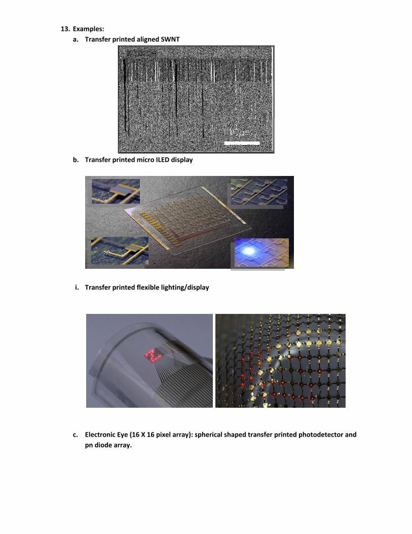
a. Transfer printed aligned SWNT
b. Transfer printed micro ILED display
i. Transfer printed flexible lighting/display
c. Electronic Eye (16 X 16 pixel array): spherical shaped transfer printed photodetector and
pn diode array.
1 cm
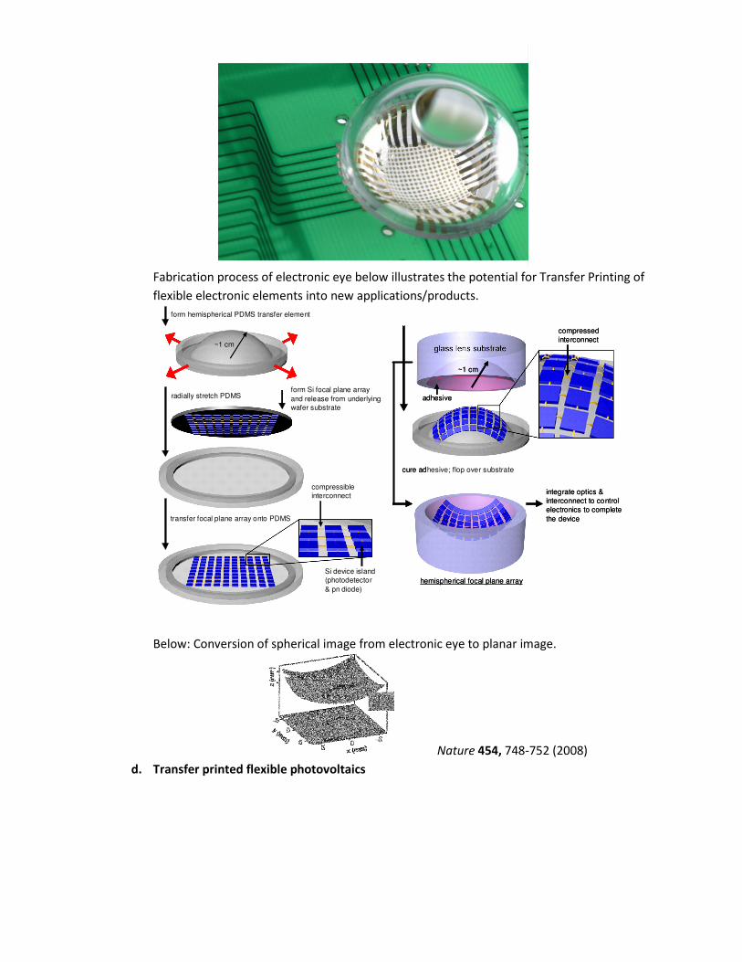
Fabrication process of electronic eye below illustrates the potential for Transfer Printing of
flexible electronic elements into new applications/products.
Below: Conversion of spherical image from electronic eye to planar image.
Nature 454, 748-752 (2008)
d. Transfer printed flexible photovoltaics
cure adhesive; flop over substrate
hemispherical focal plane array
integrate optics &
interconnect to control
electronics to complete
the device
compressed
interconnect
~1 cm
adhesive
cure adhesive; flop over substrate
hemispherical focal plane array
integrate optics &
interconnect to control
electronics to complete
the device
compressed
interconnect
~1 cm
adhesive
form hemispherical PDMS transfer element
radially stretch PDMS
transfer focal plane array onto PDMS
form Si focal plane array
and release from underlying
wafer substrate
compressible
interconnect
Si device island
(photodetector
& pn diode)
~1 cm

e. Transfer printed Si Photovoltaic array with micro-concentrators
Nature Materials 7, 907 (2008)
i. Transfer printing electronics examples
CMOS on SOI CMOS on Glass
2 mm
Aligned Misaligned
3 mm
Lenticular lens arrays
Metal interconnect
µµµµ-cell arrays 397 µµµµm
x
zy
50 µm

Semprius/Kodak, SID 2009
f. Flexible Electronics Applications: From successful project that demonstrated use of
Transfer Printing of flexible electronics process.
g. Transfer printed stretchable Si Integrated Circuits: Stretchable device and interconnect
systems are designed so that most of the buckling/strain occurs at the interconnects.
0.5 mm
Flexible electronics placed around inside wall replacing old electronics section allowing for more explosive charge.

PNAS 105, 18675 (2008)
h. Transfer printed flexible electronic sensor examples
Active neural sensor array – EcoG Tapes
500 um
0.5 mm
500

Surgeon’s glove with flexible sensors
i. Transfer printed Si CMOS on paper
j. Multi-layer transfer printed 3-layer stack solar cells
3r
200

k. Stretchable electronics for brain monitoring

1 mm
- 288 (16××××18) Sensor Array- Multiplexing Capability- 288××××7=2016 transistors

l. Thin, flexible electronic sensor patch with biodegradable silk base for improved contact
with brain surface.
Three layers 1st active layer

Nature Materials, 18 April 2010|doi:10.1038/nmat2745
m. Epidermal Electronic Patch…ultrathin complex devices that can be laminated to the skin
incorporating electrophysiological, temperature, strain sensors, as well as transistors,
light-emitting diodes, photodetectors, radio frequency inductors, capacitors, oscillators
and rectifying diodes to measure electrical activity produced by the heart, brain and
skeletal muscles…all of which can be hidden under a tattoo.
Science 333, 838 (2011); DOI: 10.1126/Science. 1206157