pdf (425Kb) - Microsystems Technology Laboratories - MIT
97
Modeling of Chemical Mechanical Polishing for Shallow Trench Isolation by Terence Gan Submitted to the Department of Electrical Engineering and Computer Science in Partial Fulfillment of the Requirements for the Degrees of Bachelor of Science in Electrical Science and Engineering and Master of Engineering in Electrical Engineering and Computer Science at the MASSACHUSETTS INSTITUTE OF TECHNOLOGY May 8, 2000 Copyright 2000 Massachusetts Institute of Technology. All rights reserved. Author__________________________________________________________________ Department of Electrical Engineering and Computer Science May 8, 2000 Certified by______________________________________________________________ Duane S. Boning Associate Professor of EECS, Thesis Supervisor Accepted by_____________________________________________________________ Arthur C. Smith Chairman, Department Committee on Graduate Theses
Transcript of pdf (425Kb) - Microsystems Technology Laboratories - MIT

Modeling of Chemical Mechanical Polishingfor Shallow Trench Isolation
byTerence Gan
Submitted to theDepartment of Electrical Engineering and Computer Sciencein Partial Fulfillment of the Requirements for the Degrees of
Bachelor of Science in Electrical Science and Engineeringand Master of Engineering in Electrical Engineering and Computer Science
at the
MASSACHUSETTS INSTITUTE OF TECHNOLOGY
May 8, 2000
Copyright 2000 Massachusetts Institute of Technology. All rights reserved.
Author__________________________________________________________________
Department of Electrical Engineering and Computer Science
May 8, 2000
Certified by______________________________________________________________
Duane S. Boning
Associate Professor of EECS, Thesis Supervisor
Accepted by_____________________________________________________________
Arthur C. Smith
Chairman, Department Committee on Graduate Theses

2
Modeling of Chemical Mechanical Polishingfor Shallow Trench Isolation
byTerence Gan
Submitted to theDepartment of Electrical Engineering and Computer Science
May 8, 2000
In Partial Fulfillment of the Requirements for the Degrees ofBachelor of Science in Electrical Science and Engineering
and Master of Engineering in Electrical Engineering and Computer Science
ABSTRACT
Shallow trench isolation (STI) has emerged as the primary technique for deviceisolation for advanced ULSI CMOS technologies. STI is desirable because it has nearzero field encroachment, good latch-up immunity, good planarity, and low junctioncapacitance. STI is also highly scalable, and trench-fill capabilities are the only majorchallenge to scaling. However, STI requires a planarization procedure, such as chemicalmechanical polishing (CMP). CMP not only increases the process complexity, but alsosuffers from die-level layout pattern dependencies which makes it difficult to completelyremove the oxide above the large nitride areas. This problem can be solved using reversetone etch back, which removes the oxide over large nitride areas prior to CMP. A modelfor reverse tone etch back is needed to obtain knowledge and insight that will reducedevelopment cycle times and cost. This thesis presents a comprehensive model forreverse tone etch back STI CMP that incorporates density averaging effects for small pre-CMP step height. STI CMP characterization experiments are performed and the resultsare used to validate the proposed model. Using the model, the effects of pre-CMP stepheight, pattern density, polish time, pad hardness, and slurry selectivity on dishing anderosion are predicted.
Thesis Supervisor: Duane S. BoningTitle: Associate Professor of EECS

3
Acknowledgements
My first thanks go out to my academic and thesis advisor Professor DuaneBoning, to whom I am extremely honored and grateful for inviting me to join his researchgroup in Fall of 1998. Even though my progress in research was slow and results werescant, he never ceased to inspire me with new research ideas and provide me withnumerous opportunities to expand my knowledge of CMP. This work is the culminationof his trust in me. I hope that I have made him proud.
Most of my experimental work was done at the Taiwan SemiconductorManufacturing Company (TSMC) in Hsin-Chu, Taiwan, as part of the MicrosystemsIndustrial Group (MIG) program at the MIT Microsystems Technology Laboratories(MTL). I wish to thank Vicky Diadiuk, Assistant Director of Operations at MTL, as wellas the staff at MTL, TSMC, the Taipei Economic and Cultural Office in Boston, and theMIT International Students Office, for working so hard to make my Summer internship atTSMC possible.
Many thanks go out to all my colleagues and friends at TSMC who were suchwarm and hospitable hosts. First of all, I wish to thank Dr. Shang-Yi Chiang, VicePresident, R&D, TSMC, for giving me this opportunity to work in TSMC; my mentorsDouglas Yu and Simon Jang, who made sure that I had all the help I needed; C. L.Chang, who was like a big brother and always there to help me whenever I encounteredproblems; C. H. Lin and H. T. Lin for teaching me how to use L-Edit to create the STICMP characterization masks; T. I. Bao for lending me his bicycle, on which I commutedto work almost everyday; F. Y. Wang for her friendship; H. W. Lin and C. Y. Lin forteaching me how to operate the SEM; J. Y. Cheng, Y. H. Chen, C. Y. Fu, T. Shih, L. Y.Su, J. M. Peng and others in the TFD R&D group for their friendship. Last but not least, Iwish to thank the engineers, support staff and operators in Fab 3 and 4 who helped me inone way or another.
I will also like to thank Mr. Tan Su Bin and family who lived next door to me inTaiwan. They were like a host family to me, making sure I was well settled in and neverhungry or lonely.
Here at MIT, I wish to thank the technical staff at MTL: Kurt Broadrick, BarryFarnsworth, Paul Tierney, and Joe Walsh just to name a few; my colleagues in theMetrology Group: Brian Lee for the interesting discussions about CMP and help withSiCat, Tamba Tugbawa for modeling insight and from whose work I have greatlybenefited, Tae Park for his invaluable help with Cadence, Vikas Mehrotra, Shiou-LinSam, Radhika Dutt, David White, Angie Nishimoto, Charles Oiji, and Dennis Ouma; myoffice mates Aaron Gower and Kuang Han Chen for their help with Matlab.
Special thanks go to Dawen Choy, Jessica Tan, Philip Tan, and Tracey Ho, for allthe sumptuous dinners we prepared together, and I could always rely on them for someentertainment after a hard day’s work. I also wish to thank all my friends in the SingaporeStudents Society, the Malaysian Students Association, and all my other friends in MITfor making my four years here so memorable. Special mention goes to my friends in theMIT Figure Skating Club, with whom I spent almost all my weekends: my coach LouiseSilver, my skating partner Angela Yu, Joyance Meechai, Bev Thurber, Bill Rowe, Barb

4
Cutler, Derek Breuning, Esther Horwich, Trish Fleming, Sally DeFazio, John Porter, andothers.
My deepest thanks go to my family in Singapore: my dad, mom, and brother,whose moral support and encouragement have given me the confidence to come this far. Ialso wish to thank my grandma, I pray you live a long and healthy life; auntie Annie, nowI hope I will be able to go travelling with you as promised; auntie Nancy and uncle Peter,thanks for your encouragement; and my darling cousins Alicia, Arena, and Amelia, Ihope to be a good role model for you. Finally, there is a special place in my heartreserved for my girlfriend, Meizhen. I do not know how to thank you enough for helpingme stay focused on my work, and loving me from halfway around the Earth.
Last but not least, I thank my sponsor, the Singapore Economic DevelopmentBoard. With your financial support, I was able to come to MIT and need not worry abouthaving enough money to pay my tuition.
To all my family and friends, I dedicate this work to you.
This work was supported in part by a DARPA subcontract with PDF Solutions,Inc.

5
Table of Contents
Chapter 1 Introduction................................................................................................... 10
1.1 Motivation for Device Isolation ............................................................................ 11
1.2 Device Isolation Techniques ................................................................................. 13
1.2.1 Local Oxidation of Silicon ........................................................................ 13
1.2.2 Shallow Trench Isolation........................................................................... 16
1.3 Thesis Goals .......................................................................................................... 18
1.4 Thesis Organization............................................................................................... 19
Chapter 2 Chemical Mechanical Polishing for STI ..................................................... 20
2.1 Overview of Dielectric CMP................................................................................. 20
2.2 Shallow Trench Isolation CMP ............................................................................. 23
2.3 Reverse Tone Etch Back STI ................................................................................ 25
Chapter 3 Modeling of Reverse Tone Etch Back STI CMP........................................ 27
3.1 Previous Work....................................................................................................... 28
3.1.1 Density Dependent CMP Model ............................................................... 28
3.1.2 Removal Rate vs. Step Height CMP Model.............................................. 29
3.2 Model Formulation................................................................................................ 30
3.3 Mathematical Relations......................................................................................... 34
3.3.1 Steady State Dishing ................................................................................. 35
3.3.2 Step Height ................................................................................................ 35
3.3.3 Nitride Erosion .......................................................................................... 37
3.4 Experimental Details ............................................................................................. 38
3.4.1 The STI CMP Characterization Mask ....................................................... 38
3.4.2 Process Conditions .................................................................................... 42
3.5 Parameter Extraction Methodology....................................................................... 43
3.6 Results and Discussion.......................................................................................... 45
3.6.1 Oxide-Nitride Selectivity .......................................................................... 51

6
3.6.2 Polish Time Constant, τ............................................................................. 51
3.6.3 Steady State Dishing, dss ........................................................................... 52
3.6.4 Pad Deformation Limit, dmax ..................................................................... 53
3.7 Additional Modeling Results ................................................................................ 55
3.7.1 Pattern Density .......................................................................................... 55
3.7.2 Initial Step Height ..................................................................................... 58
3.7.3 Oxide to Nitride Selectivity....................................................................... 60
Chapter 4 Combined Planarization Length Parameter Extraction Methodology.... 62
4.1 Density Averaging using Planarization Length..................................................... 63
4.2 Updated Parameter Extraction Methodology........................................................ 66
4.3 Results and Discussion.......................................................................................... 68
Chapter 5 Conclusion and Future Work ...................................................................... 71
5.1 STI CMP Modeling............................................................................................... 71
5.2 Applications of the Methodology.......................................................................... 72
5.3 Future Work .......................................................................................................... 73
5.3.1 Validation on Non-Standard Structures .................................................... 73
5.3.2 Process Variations ..................................................................................... 73
5.3.3 Steady-State Dishing (dss) and Pad Deformation Limit (dmax) .................. 74
5.3.4 Kox and Knit ................................................................................................ 74
Bibliography .................................................................................................................... 75
Appendix .......................................................................................................................... 78
A-1 Planarization Length Optimization for Process A................................................. 78
A-2 Density and Parameter Extraction for Process A .................................................. 79
A-3 Cost Function for Process A.................................................................................. 80
B-1 Planarization Length Optimization for Process B................................................. 83
B-2 Density and Parameter Extraction for Process B .................................................. 84
B-3 Cost Function for Process B.................................................................................. 85
C-1 Planarization Length Optimization for Process C................................................. 88

7
C-2 Density and Parameter Extraction for Process C .................................................. 89
C-3 Cost Function for Process C.................................................................................. 90
D Effective Density Extractor ................................................................................... 93
E Density Map Generator ......................................................................................... 94
F Density Averaging................................................................................................. 95
G Matrix Shift ........................................................................................................... 97

8
List of Figures
1.1 Parasitics in NMOS transistor .................................................................................. 12
1.2 Parasitics in CMOS transistor .................................................................................. 12
1.3 Simplified pnpn thyristor model for a CMOS inverter ............................................ 13
1.4 LOCOS process summary........................................................................................ 15
1.5 STI process summary............................................................................................... 17
2.1 Examples of CMP tools............................................................................................ 21
2.2 Possible oxide CMP mechanism.............................................................................. 22
2.3 Effect of pad rigidity on planarity ............................................................................ 23
2.4 Problems with conventional STI CMP..................................................................... 24
2.5 Modified process flow for reverse tone etch back STI CMP................................... 26
3.1 Cross-section of a reverse tone etch back STI structure .......................................... 31
3.2 Removal rate vs. step height model for reverse tone etch back STI CMP............... 32
3.3 Close-up of STI CMP characterization masks ......................................................... 39
3.4 Schematic of STI CMP characterization mask......................................................... 41
3.5 Actual and predicted step height for process A........................................................ 48
3.6 Actual and predicted step height for process B........................................................ 49
3.7 Actual and predicted step height for process C........................................................ 50
3.8 Dependence of τ, dss, and dmax on density ................................................................ 54
3.9 Time evolution of step height and nitride erosion on pattern density...................... 57
3.10 Effect of pre-CMP step height on post-CMP step height......................................... 59
3.11 Effect of high selectivity slurry on step height and nitride erosion.......................... 61
4.1 Physical meaning of planarization length ................................................................ 63
4.2 Density averaging..................................................................................................... 64
4.3 Effective density distribution for different planarization lengths ............................ 65
4.4 Flow chart of updated parameter extraction methodology....................................... 67
4.5 Effective density vs. pattern density......................................................................... 70

9
List of Tables
3.1 Summary of CMP conditions ................................................................................... 43
3.2 Summary of results from parameter extraction........................................................ 46
3.3 RMS errors for step height and nitride erosion ........................................................ 47
4.1 RMS errors using the updated parameter extraction methodology.......................... 69
5.1 Expected and extracted values for Kox, Knit, and selectivity..................................... 74

10
Chapter 1Introduction
Shallow trench isolation (STI) has emerged as the primary technique for device
isolation for advanced ULSI CMOS technologies [1]-[3]. DRAM and microprocessor
products are currently the technology drivers for the whole semiconductor industry. The
International Technology Roadmap for Semiconductors predicts that DRAM half-pitch
and microprocessor gate length will reach 100 nm and 65 nm respectively in 2005, from
180 nm and 140 nm today. In the same period, the transistor density for logic (high-
volume microprocessor) at introduction is expected to increase from 6.6 million
transistors per cm2 per chip to 44 million transistors per cm2 [4]. This is driven by the
need to maintain the historical trend of reducing cost per function by 25-30% per year
while accommodating 59% more bits/capacitors/transistors per year in accordance with
Moore’s Law [4]. To satisfy the high density requirements of modern integrated circuits,
device isolation is needed. STI is the preferred technique for deep sub-micron
applications.
This chapter summarizes the main techniques and issues in device isolation.
Section 1.1 discusses the reasons for device isolation. Section 1.2 presents an overview of
some isolation techniques and their limitations. Section 1.3 defines the scope of this
thesis, and finally, Section 1.4 details the thesis organization.
11
1.1 Motivation for Device Isolation
An important part of integrated circuit design is directed towards keeping the
basic device characteristics as close to ideal as possible. This means reducing parasitic
conduction paths and series resistances, maintaining threshold voltage control, and
minimizing the leakage current of the device. However, in order to increase the gross
number of chips available on a wafer, a combination of smaller feature sizes (scaling and
shrink) and product redesign (compaction) is used. Compaction reduces the separation
between adjacent devices, which increases the chance of device failure via parasitic
conduction paths and latch up. Device isolation can prevent parasitic conduction and
latch up and this is discussed below.
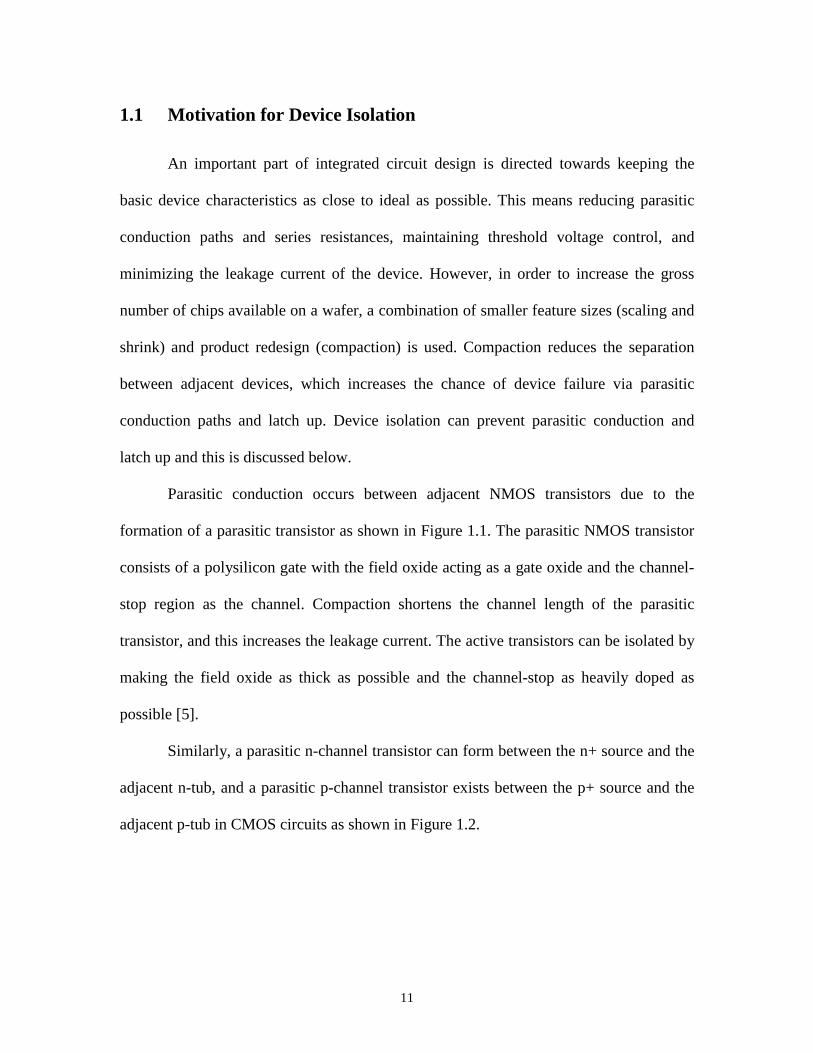
Parasitic conduction occurs between adjacent NMOS transistors due to the
formation of a parasitic transistor as shown in Figure 1.1. The parasitic NMOS transistor
consists of a polysilicon gate with the field oxide acting as a gate oxide and the channel-
stop region as the channel. Compaction shortens the channel length of the parasitic
transistor, and this increases the leakage current. The active transistors can be isolated by
making the field oxide as thick as possible and the channel-stop as heavily doped as
possible [5].
Similarly, a parasitic n-channel transistor can form between the n+ source and the
adjacent n-tub, and a parasitic p-channel transistor exists between the p+ source and the
adjacent p-tub in CMOS circuits as shown in Figure 1.2.

12
Figure 1.1 Parasitic transistor in NMOS: (a) top view of adjacent NMOS transistorssharing a common gate, (b) cross-section view showing the npn parasitictransistor.
Figure 1.2 Parasitics in CMOS transistor: (a) top view of adjacent n- and p-channeltransistors sharing a common polysilicon gate, (b) parasitic n- and p-channels.
Latch up occurs in CMOS circuits when the source/drain regions are in close
proximity to an adjacent tub. The source/drain regions and the tubs form parasitic bipolar
transistors that make up a thyristor (pnpn) device as shown in Figure 1.3. The thyristor
can be biased such that the collector current of the pnp device supplies a base current to
the npn device in a positive feedback arrangement. This produces a large sustained
current between the positive and negative terminals of the thyristor and may cause the
CMOS circuit to cease functioning or even self-destruct [5]. The parasitic bipolar
n+ well
p substrate
oxide
polysilicon gate
parasitic transistor
active transistor
parasitic transistor
(a) (b)
p+ channel stop
n+ p+
n tubp tub
n-channelisolation
p-channelisolation
polysilicon gate
n tubp tub
oxide
parasitic n-channel parasitic p-channel
(a) (b)

13
transistors can be decoupled in several ways, including physically separating the
transistors via trench isolation.
Figure 1.3 Simplified pnpn thyristor model for a CMOS inverter.
1.2 Device Isolation Techniques
In integrated circuits, devices such as transistors are fabricated on a common
piece of silicon. Without proper device isolation, these devices will interact with one
another in undesirable ways. The need for a scalable CMOS isolation technology is
critical in order to advance into the 0.25 µm 256Mbit DRAM generation and beyond. The
geometric characteristics of ideally scalable isolation technology are (1) an abrupt
transition from active MOSFET regions to isolation regions, (2) independence of
isolation width and depth, and (3) planarity [3]. This section describes the key features of
two of the most well-known device isolation techniques for ULSI applications: LOCOS
and shallow trench isolation (STI).
1.2.1 Local Oxidation of Silicon
Local oxidation of silicon (LOCOS) has been the most dominant isolation process
used in IC technologies for the last two decades, mainly due to simplicity and low cost.
p+ n+ p+ n+
n-well

14
However, as semiconductor devices scale down to sub-0.5 µm geometries, the
practicality of conventional LOCOS is questioned. The main drawbacks of conventional
LOCOS are bird’s beak formation, field-implant encroachment, field oxide thinning at
narrow dimensions, and topography [3,6].
LOCOS utilizes the property that oxygen diffuses through silicon nitride (Si3N4)
very slowly, so a thick layer of oxide (SiO2) can be preferentially grown to laterally
isolate devices. Figure 1.4 shows the major process steps. A thin layer of pad oxide is
first thermally grown on a clean silicon surface. Next, a thick layer of chemical vapor
deposition (CVD) silicon nitride, which functions as the oxidation mask, is deposited.
The nitride/oxide composite layer is then patterned and etched, followed by a field
implant to form the channel-stop. The wafer is then oxidized. The nitride acts as a barrier
to the diffusion of oxygen and prevents oxidation of the silicon below the nitride. Since
oxidation consumes 44% as much silicon as it grows, the resultant oxide is partially
recessed. Lateral diffusion of oxygen under the edges of the nitride causes some silicon
under the nitride to be oxidized. The process leaves a characteristic structure called a
bird’s beak because it is shaped like the beak of a bird. Finally, the masking nitride layer
is stripped and the pad oxide is etched [7,8].
The existence of the bird’s beak reduces the amount of current that a transistor can
drive. As shown in Figure 1.3, the bird’s beak encroaches laterally into the silicon under
the nitride. This reduces the active width of the device, which reduces its drive current.
In order to grow the thick layer of oxide needed for device isolation, high
temperatures and long oxidation times are needed. The high thermal budget causes the

15
dopants in the channel-stop to diffuse into the edges of the active region. The resultant
transistor behaves as if it is a narrower device, and this further reduces its drive current.
Figure 1.4 LOCOS process summary: (a) pad oxide and nitride deposition, (b) patternand etch, (c) oxide growth, (d) nitride and pad oxide stripping.
LOCOS also suffers from field oxide thinning which degrades planarity and
results in shallow isolation. The thickness of the field oxide varies strongly with isolation
space. In particular, field oxide thinning increases with decreasing isolation space [3,6].
Hence, it creates topography between wide isolation regions and narrow isolation
regions. Furthermore, LOCOS-based isolations are shallow because more than half of the
as-grown oxide thickness is above the silicon surface. Field oxide thinning causes the
junction to be even shallower, and the junction may not be sufficiently deep to keep
isolation implants from impacting junction and device characteristics [3].
As mentioned earlier, more than half of the as-grown oxide thickness is above the
silicon surface. Hence, LOCOS creates significant topography. Non-planarity results in
poor linewidth control during subsequent lithographic and etching processing [3].
Traditional LOCOS has serious has many serious limitations in the sub-
micrometer regime that limit the minimum active area pitch that can be achieved. Several
nitride
pad oxide
silicon
bird’s beak
field oxide
(a)
(b)
(c)
(d)

16
advanced LOCOS processes have been proposed, that reduce the minimum active area
pitch to 0.9 µm and 0.6 µm for 64 Mbit and 256 Mbit DRAM respectively. However, for
pitch values below 0.6 µm, the field oxide thinning effect inherent in all LOCOS-based
technologies, results in unacceptable parasitic field devices characteristics [10].
1.2.2 Shallow Trench Isolation
Shallow trench isolation (STI) is the preferred isolation scheme for applications
based on ULSI CMOS technologies with active area pitches in the sub-0.5 µm regime.
STI is preferred over LOCOS because it has near zero field encroachment, good latch-up
immunity, better planarity, and low junction capacitance [1,2,3]. STI is also highly
scalable, the trench-fill capabilities being the only major challenge to scaling [3].
However, STI requires a planarization procedure that increases the process complexity.
STI is fabricated using a damascene process. Figure 1.5 shows the major STI
process steps. A thin layer of pad oxide is first grown on a clean silicon surface. A thick
layer of CVD nitride is then deposited on top of the oxide. The nitride is subsequently
patterned and a trench is anisotropically etched into the silicon substrate. After resist
stripping, the trench sidewalls are passivated with a thin layer of thermal oxide. The
trenches are then filled with a thick CVD oxide and subsequently planarized using
chemical-mechanical polishing (CMP), stopping on the nitride layer. Finally, the nitride
barrier and pad oxide are removed.

17
Figure 1.5 STI process flow summary: (a) pad oxide and nitride deposition, (b)anisotropic trench etch, (c) trench sidewall passivation, (d) trench fill, (e)CMP planarization, (f) nitride and pad oxide strip.
STI is able to achieve near zero field encroachment because an anisotropic etch is
used to form the isolation trenches. The sidewalls are nearly vertical, and the angle of the
sidewalls is limited by the trench fill capability of the oxide used [3]. The width of the
isolation trenches is defined exactly by the lithography step, hence, STI can be scaled
with each technology generation.
The depth of the trenches depends on the anisotropic etch process. Trenches of
arbitrary depths can be fabricated by varying the etch time. Deeper trenches increase
latch-up immunity, decrease junction capacitance, and decrease junction leakage [3]. In
practice, the aspect ratio of the trench (ratio of height to width) is limited by the trench
fill capability of the oxide used as mentioned earlier.
Several techniques have been developed to achieve planarization and most of
them use CMP [1]-[3],[10]-[12]. However, the amount of material removed during CMP
nitride
pad oxide
silicon
CVD oxide(a) (d)
(e)
(f)(c)
(b)

18
depends on the pattern density of the active area [13], which causes uneven polishing
within a die and across a wafer. One method that effectively improves post-CMP
planarity is to use a two mask process and a combination of reactive ion etching (RIE)
and CMP (reverse tone etch back) [14]. This method uses a second mask, which is a
negative of the pattern layout, to remove the oxide in the large active areas which
normally polish slowly. This way, uneven clearing of the oxide over the active areas is
reduced.
STI appears, therefore, as the unavoidable replacement for the LOCOS-based
isolation schemes for deep sub-0.5 µm technologies and beyond. STI provides a planar
surface, does not suffer from field oxide thinning, and can be scaled down into smaller
dimensions.
1.3 Thesis Goals
The main challenge of STI is to polish the overburden oxide controllably so that
oxide removal stops once it reaches the nitride barrier. In practice, the removal rate varies
within a die and across the wafer. The modeling of these variations is an important first
step towards better process control. In particular, models that address pattern
dependencies directly from layout are needed [4]. In this thesis, a model for reverse tone
etch back for STI CMP is developed. There are currently no models for reverse tone etch
back STI CMP, although models for single-step STI CMP [11] and control methods for
STI CMP exist [15]. A model for reverse tone etch back for STI CMP is needed to obtain
knowledge and insight that will reduce development cycle times and cost. The effects on

19
CMP performance due to the type of polishing pad and polishing tool are also
investigated in this thesis.
1.4 Thesis Organization
This thesis is divided into five chapters. Chapter 2 introduces the CMP process
and explains how pattern dependencies affect STI CMP. Reverse tone etch back is
presented as an effective way to overcome uneven polishing due to variations in pattern
layout.
A model for reverse tone etch back STI CMP is developed in Chapter 3. The
model is an adaptation of a dual-material damascene CMP model proposed by Tugbawa
[16]. The proposed model is based on the dependence of oxide and nitride removal rates
on local step height. Experimental data is used to verify the modeling methodology.
An improved parameter extraction methodology using the effective density of the
die instead of the designed pattern density is developed in Chapter 4. The thesis
conclusions and suggestions for future work are presented in Chapter 5.
Finally, the parameter extraction routines are included in the appendices. The
density averaging routines written by Ouma and later modified by Lee are used in this
work, and are also included in the appendices.

20
Chapter 2Chemical Mechanical Polishing for STI
Chemical mechanical polishing (CMP) is a well-known polishing process.
Historically, it is used by skilled craftsmen to produce optically flat and mirror-finished
surfaces. It also occurs in nature, producing beautifully finished stones. In the
semiconductor industry, CMP has been used for more than 30 years to prepare silicon
wafers. In recent years, CMP has emerged as the primary technique for planarizing
dielectrics. It has also found wider application in the entire VLSI development and
production cycle serving as an enabling tool for shallow trench isolation, damascene
technologies and other novel process techniques.
In this chapter, CMP will be presented as an enabling technology for STI. Section
2.1 describes briefly the CMP process. Section 2.2 explains how CMP is used in STI and
describes some of the problems encountered during CMP of STI structures, and Section
2.3 explains how reverse tone etch back solves or reduces these problems.
2.1 Overview of Dielectric CMP
The purpose of CMP in dielectric polishing is to remove topography while
maintaining good uniformity across the entire wafer. CMP is very effective at reducing
feature-level or local step height, and achieves a measure of global planarization not
possible with spin-on and resist etch back techniques.

21
The schematic of a rotary CMP tool and a linear CMP tool are shown in Figures
2.1a and 2.1b respectively. CMP tools essentially comprise a polishing pad which moves
relative to the wafer carrier. The wafer carrier holds the wafer face down against the
polishing pad. The wafer carrier can both exert a force on the wafer and rotate the wafer
independent of the polishing pad. Polishing is usually done in the presence of a polishing
slurry that is fed automatically onto the polishing pad.
Figure 2.1 Examples of CMP tools: (a) rotary polisher, (b) linear polisher.
The exact mechanism for oxide polishing is not fully understood, and several
theories exist. One such theory describes it as a chemical-mechanical mechanism at the
microscopic level (Figure 2.2) involving: (1) forming hydrogen bonds between the oxide
on the wafer and the slurry particles; (2) forming molecular bonds between the wafer and
the slurry; and (3) breaking the oxide bonds with the wafer surface when the slurry
particle moves away [8]. Hence CMP relies on chemical-mechanical action as its name
wafer carrier
silicon wafer
polishing pad
polishing table
slurry feeder
slurry(a)
slurry feeder
slurry wafer carrier
silicon wafer polishing pad
polishing table
(b)

22
suggests, and not on mechanical abrasion. Because of the chemical effect of bond
breaking, the polishing slurry has a large effect on the polishing rate. For example,
slurries made from oxides with higher oxygen bond strengths such as cerium oxide, have
polishing rates several times higher than silica-based slurries.
Figure 2.2 Possible oxide CMP mechanism: (a) hydrolysis of oxide surface and slurryin alkaline solution, hydrogen bond formation between the slurry and theoxide surface, (b) Si-O bond formation by releasing a water molecule, (c)removal of silicon atom when slurry particle moves away.
CMP achieves planarity due to the rigidity of the polishing pad when it is in
contact with a wafer. This is illustrated in Figure 2.3. A soft pad that conforms to the
topography on the surface of the wafer removes the oxide uniformly everywhere, hence it
does not planarize the wafer. On the other hand, a rigid pad polishes the high spots at a
faster rate, hence topography can be reduced. The rigidity of the pad depends not only on
the material the pad is made from, but also on the process conditions, such as the speed of
the polishing pad and the down force on the wafer.
O O OO
Si
O
Si
O
Si
O
Si
O
Si
O
Si
H
H H H H
H
Si
H
Si
H
Si
HSi
OH
Si
OSi
(a) (b) (c)

23
Figure 2.3 Effect of pad rigidity on planarity: (a) an ideal soft pad conforms to theinitial topography and removes oxide everywhere at the same rate, (b) aninfinitely rigid pad removes material in the up area faster than in the downarea, so the final surface is flat.
2.2 Shallow Trench Isolation CMP
STI structures are formed using a damascene process, as shown previously in
Figure 1.5. The damascene process derives its name from the traditional art of inlaying
metal in ceramic or wood for decoration. Similarly, STI formation involves polishing the
overburden oxide until only oxide remains in the trenches. CMP is the preferred way to
remove the overburden oxide, but it is sensitive to pattern effects and process conditions.
The sensitivity of CMP to pattern density is well documented [13,19,20]. This
relationship is shown explicitly in the MIT model for density-dependent polish rate [19]:
RateK
=ρ
(2.1)
where K is the blanket removal rate and ρ is the density of the up area.
(a)
polishing pad
oxide
post-CMP oxide level
silicon
silicon nitride
(b)
polishing pad
oxide
post-CMP oxide level
silicon
silicon nitride

24
In conventional STI CMP, density variations in the active area cause the
overburden oxide above the low density nitride regions to be removed faster than the
oxide above the high density nitride regions. As shown in Figure 2.4a, the nitride in the
low density regions will be cleared earlier than the nitride in the high density regions. It is
thus necessary to overpolish the wafer to remove all the oxide above the nitride, as any
oxide that remains above the nitride will prevent the nitride from being completely
stripped off during the subsequent processing steps.
Figure 2.4 Problems with conventional STI CMP: (a) a realistic semi-rigid padpolishes oxide at different rates depending on the pattern density, (b) nitrideerosion and oxide dishing due to uneven polishing, (c) any oxide that is lefton top of the nitride prevents nitride stripping; overpolishing can cause theoxide to recess below the silicon.
There are two undesirable consequences of overpolishing: oxide dishing and
nitride erosion. Oxide dishing is said to occur when the top of the oxide in the trenches
recesses below the top of the nitride as shown in Figure 2.4b. Dishing occurs partly
(a)
semi-rigid pad
low density area just cleared
oxide on large features
nitride erosion
oxide dishing(b)
(c)unstripped nitride
excessively dished oxide
uncleared oxide

25
because the slurry is normally chosen so that the oxide polishes faster than the nitride.
Since the polishing pad is not infinitely rigid, it is able to deform into the trenches as the
oxide in the trenches is removed faster than the nitride in the up areas. Hence, dishing
increases the amount of topography present in a die. Overpolishing can also cause the
oxide to recess below the silicon as shown in Figure 2.4c. This is undesirable because it
degrades the quality of the isolation and may damage the edges of the silicon active area.
Nitride erosion occurs in the overpolished regions because the extra amount of polishing
causes some nitride to be removed. Thinning of the nitride layer due to erosion is a
problem because it may cause the underlying silicon active area to be damaged by CMP.
2.3 Reverse Tone Etch Back STI
Dishing and erosion can be reduced by using an additional photolithography and
RIE etch step prior to CMP. The additional process steps are shown in Figure 2.5. After
depositing the overburden oxide, the oxide is patterned using a reverse tone mask. The
reverse tone mask is basically an inverse of the mask used to pattern the wafer to form
the STI structures. Some slight biasing is applied to account for overlay errors. Hence,
the reverse tone mask defines the area of oxide above the nitride that will be removed.
The exposed oxide is removed using an RIE etch that stops on nitride. Finally, the excess
oxide in the trenches is removed using CMP.
The purpose of the reverse tone etch back step is to remove most of the
overburden oxide above the nitride, especially the oxide in the large nitride areas which
are difficult to remove during conventional STI CMP. Hence, the CMP step is now
concerned only with removing the excess oxide in the trenches to reduce topography.

26
However, the removal of the excess oxide is still density dependent and some regions
will polish faster than others. Fortunately, the requirements for this are less stringent
(than requiring that all the oxide above the nitride be removed), thus the amount of
overpolishing can be reduced. This helps to reduce dishing. Unfortunately, because the
nitride is already exposed prior to CMP, this process may increase the amount of nitride
erosion. This can be solved by using slurries with higher oxide to nitride selectivity.
Figure 2.5 Modified process flow for reverse tone etch back STI CMP: (a) cross-section of STI structure after oxide deposition, (b) reverse tone etch back ofmost of the overburden oxide above the nitride area, (c) post-CMP profileshowing dishing and erosion, (d) nitride and pad oxide strip.
The reverse tone etch back process is expensive because it requires an additional
photolithography step. Several other methods of planarizing the wafer prior to CMP have
been proposed, such as using dummy fill [1,17], selective oxide deposition [12], and
spin-on films [18]. However, reverse tone etch back is still commonly used because it is
the most effective in reducing the post-CMP difference in step height between small and
large active areas [1].
(a)
(b)
(c)
(d)

27
Chapter 3Modeling of Reverse Tone Etch Back STICMP
Shallow trench isolation (STI) is an enabling process for advanced ULSI
technologies. It can be scaled to fine dimensions while maintaining good planarity, good
latch-up immunity, and low junction capacitance. However, the CMP process is density
dependent and single-step STI CMP can lead to significant oxide dishing and nitride
erosion problems. Hence, an additional etch back step is commonly used before CMP to
remove the overburden oxide over large active areas. The resulting CMP process is
concerned only with removing the excess oxide in the trenches until the oxide reaches the
same level as the nitride. This is a complicated process that depends on the relative
removal rate of the oxide in the trenches and the nitride barrier in the raised area, as well
as the pattern density. There are currently no existing models for reverse tone etch back
STI CMP, even though models for single-step STI CMP and process control methods
exist. In this chapter, a mathematical model for reverse tone etch back STI CMP based on
density and step height dependent oxide and nitride removal rates is presented.
Some previous work on CMP modeling is presented in Section 3.1. The reverse
tone etch back STI CMP model is described in detail in Section 3.2. Section 3.3 explains
how the equations for step height (or dishing) and nitride erosion are derived from the
model. Section 3.4 describes the experiments and the STI characterization mask used to
pattern the wafers that are used in this modeling work. The method for extracting the

28
model parameters is explained in Section 3.5. The model and actual measurements are
compared in Section 3.6. Additional modeling results are shown in Section 3.7.
3.1 Previous Work
The model presented here is a culmination of previous work performed at the
Massachusetts Institute of Technology: Stine et al. demonstrated the strong relationship
between CMP removal rate and pattern density [19], Smith et al. described integrated
pattern density and step height models for oxide CMP [20], and Tugbawa et al. proposed
a removal rate vs. step height model for dual-material damascene CMP [16].
3.1.1 Density Dependent CMP Model
The basic MIT density model for dielectric CMP provides a first-order
approximation of post-polish dielectric thickness for arbitrary layouts [19]-[21]. The
model is derived from Preston’s equation, and assumes that the polishing rate of a raised
area is equal to the blanket rate divided by its effective density as shown in equation
(2.1). However, the model assumes that no down area polishing occurs until the local step
height is removed. Once the step height is removed, the model assumes that the removal
rates of both the raised and down areas equal the blanket rate.
Grillaert et al. found that, for small step heights, polish occurs in both up and
down areas, in contrast to up area contact only for large steps [22]. Based on this effect,
Smith et al. improved the density based polish model by combining effective density and
time dependencies which take into account the time at which the pad contacts the down

29
areas. Using this methodology, Smith demonstrated a 50% improvement in fit to
experimental data over the original density model.
3.1.2 Removal Rate vs. Step Height CMP Model
Tugbawa et al. proposed a dual-material damascene CMP model based on the
relationship between removal rate and step height during CMP [16]. The model
incorporates the following key observations used by Smith. (1) Polishing pads are not
infinitely hard and may deform into a space, and the step height at which the pad contacts
the down area, dmax, is determined by the properties of the pad and pattern density
[20,21,22]. (2) For step heights larger than dmax, the up areas polish at a rate given by the
MIT density model. (3) For step heights smaller than dmax, the up area removal rate
decreases with decreasing step height while the down area removal rate increases with
decreasing step height. (4) Changes in step height cease once the up area removal rate
becomes the same as the down area removal rate. Tugbawa captured these observations
into a removal rate vs. step height plot, from which equations describing dual-material
CMP can be derived.
The removal rate vs. step height model also unifies several observations from
other CMP models: (1) Burke proposed that step height decreases exponentially with
time [23]; (2) Tseng et al. proposed that the removal rates of raised and down areas
converge exponentially to the blanket removal rate as polish time increases [24]; (3) the
IMEC model proposed that step height at which the pad contacts the down area is a
function of the feature density [22].

30
The removal rate vs. step height model should work for any CMP process, but it
is extremely useful for modeling damascene processes like copper CMP or STI CMP,
where simultaneous polishing of more than one material is involved. The reverse tone
etch back STI CMP model presented here is an adaptation of Tugbawa’s dual-material
damascene CMP model, which greatly simplifies the analysis of reverse tone etch back
STI CMP into a simple graph as shown in the next section.
3.2 Model Formulation
Chemical mechanical polishing (CMP) as its name suggests, achieves global
planarity through a combination of chemical action from the slurry and mechanical action
from the polishing pad and slurry particles. The slurry chemistry can be adjusted for
varying degrees of selectivity between different materials, but the contact between the
polishing pad and the wafer is the main mechanism for removing the local step height
that causes planarization. In STI CMP, we are interested in changes in step height
(especially dishing) and nitride erosion. This makes a step height based model a
convenient starting point. Furthermore, when analyzing step height changes, we do not
overload ourselves with the details of the physical or chemical aspects of CMP. Instead,
we take a broader perspective of the sum of all contributing factors. From the
measurement point of view, changes in local step height are also easier to measure.

31
Figure 3.1 Cross-section of a reverse tone etch back STI structure showing nitrideerosion and step height after CMP.
Before delving into the model, we first define step height (dishing) and nitride
erosion as shown in Figure 3.1. Figure 3.1 shows the cross section of a reverse tone etch
back wafer before and after CMP. The local step height is the vertical distance between
the top of the nitride and the top of the oxide. It is positive when the oxide is above the
nitride, and negative when the oxide recesses below the nitride. Negative step height is
also known as dishing. Nitride erosion is simply the amount of nitride loss due to CMP.
As shown, the reverse tone etch back process leaves a narrow region of oxide
remaining on the nitride up areas. The amount of overlap depends on the design of the
reverse tone etch back mask. For this work, the overlap is measured to be 0.2 µm. For
nitride widths greater than 8 µm, the overlap reduces the exposed nitride area by less than
10%, based on a square active area. Hence, in this work, we assume that the area of the
exposed nitride is approximately the designed area since features with much larger
dimensions are used.
step height
0
nitride erosion
CMP
silicon
silicon nitride
oxide

32
Figure 3.2 Removal rate vs. step height model for reverse tone etch back STI CMP.
The model can be explained graphically in Figure 3.2, which shows how the
oxide and nitride removal rates on a reverse tone etch back STI wafer change with step
height. The vertical axis measures the oxide removal rate in the STI trenches (RRox), and
the nitride removal rate in the active areas (RRnit). The horizontal axis measures the local
step height. From the way the graph is drawn, we can infer that polishing progresses from
the right to the left of the graph (from positive step height to negative step height) as
indicated by the arrows. The graph with the upper arrow is for oxide CMP, and the one
with the lower arrow is for nitride CMP.
As mentioned earlier, this model recognizes that polishing pads are not infinitely
hard. When a pad is in contact with a wafer, it is supported mostly by the up areas of the
wafer. However, the pad also deforms into the spaces between the up areas. If the local
step height is very high, the pad will not contact the down area, and there will be no down
area polishing. The up area (oxide) polish rate in this case is density dependent and given
by the expression RRox
Kox= −1 ρ , where Kox is the blanket oxide removal rate, and ρ is the
nitride density.
RRox, RRnit
Kox
Knit
-dss dmax
Kox
1− ρ
Step Height

33
As the wafer polishes, only the oxide in the up areas are removed and this causes
the local step height to decrease. At some critical step height denoted by dmax, the pad just
touches the down area (nitride). The pad is now supported by both the up and down areas.
The down area removal rate is now non-zero. Additional polishing further reduces the
local step height which increases the force of contact between the pad and the down area
while it decreases the force between the pad and the up area. This causes the down area
removal rate to increase and the up area removal rate to decrease. For simplicity, the
model assumes that the down area removal rate increases linearly and the up area
removal rate decreases linearly with decreasing step height as shown in Figure 3.2. This
is verified experimentally.
When the local step height is zero, we postulate that the down area removal rate is
equal to Knit, the blanket nitride removal rate. Similarly, the up area polish rate is equal to
Kox, the blanket oxide removal rate. Ideally, we want to stop polishing at this point since
we have removed the local step height as desired. In reality, different points on a wafer
achieve local planarity at different times. Hence, overpolishing is necessary, and this
causes the oxide to recess below the nitride. When the oxide recesses below the nitride,
we say that dishing has occurred. As long as the oxide removal rate is higher than the
nitride removal rate, the amount of dishing increases with polish time. Eventually, the
oxide removal rate and nitride removal rate become equal and steady-state dishing
occurs. We denote this point by dss in Figure 3.2.

34
3.3 Mathematical Relations
Figure 3.2 contains all the information needed to completely model the reverse
tone etch back STI CMP process. In fact, the model can be described completely using
only four variables: the density-independent oxide removal rate (Kox), the density-
independent nitride removal rate (Knit), the effective pattern density ρ, and the pad
deformation limit (dmax). The graphs in Figure 3.2 can be described mathematically as
follows:
Oxide Removal Rate RR
KH d
KH
dd H d
ox
ox
ox ss
,
max
maxmax
=−
>
+−
− < <
1
11
ρ
ρρ
(3.1)
Nitride Removal Rate RR
H d
KH
dd H d
nit
nit ss
,max
maxmax
=>
−
− < <
0
1
(3.2)
where H is the step height. Using these equations, the following useful relations can be
derived.

35
3.3.1 Steady State Dishing
The amount of steady state dishing is the maximum distance the oxide in the
trenches can recess below the nitride. In STI CMP, we want the level of the post-CMP
oxide to be above the silicon. Thus the amount of steady state dishing determines the
minimum nitride thickness required, assuming no nitride loss during CMP. By definition,
steady state dishing occurs when the oxide and nitride removal rates are equal. Equating
equations (3.1) and (3.2), the expression for steady state dishing is
( ) ( )( )d
K K d
K Kssox nit
nit ox
=− −− +
1
1
ρρ ρ
max (3.3)
3.3.2 Step Height
Ideally, polishing should stop when the features are planar, that is, when the local
step height is zero. The amount of polishing required can be easily calculated if the time
evolution of step height is known. The rate of change of step height is given by the
difference in the oxide removal rate and the nitride removal rate:
dH
dtRR RRox nit= − (3.4)
Integrating this gives the expression for step height:

36
( )
( )H t
dK
t H d
d d d e H d
ox
ss
t tc
=
− >
− + −
<
−−
0
1
ρ
τ
max
max max max
(3.5)
where the exponential time constant τ and the touch down time tc are given by:
( )( )τ
ρρ ρ
=−
− +d
K Knit ox
max 1
1(3.6)
( ) ( )t
d d
Kcox
=− −0 1max ρ
(3.7)
The exponential time constant, τ, is a measure of how fast a given process can
achieve planarity. The touch down time, tc, is the amount of polishing required before the
pad contacts the down areas. The local step height before CMP is given by d0. The above
expressions are valid in general, but if d0 < dmax, we can simplify equation (3.5) to:
( ) ( )H t d d d ess
t
= − + −
−
0 0 1 τ (3.8)

37
3.3.3 Nitride Erosion
The nitride layer is used as a barrier layer to protect the underlying silicon from
damage during CMP. Ideally, the nitride removal rate is zero. In practice, depending on
the process used, nitride loss can be significant. The amount of nitride loss during CMP
determines the amount of overpolishing that can be tolerated and the thickness of the
nitride layer needed. The expression for nitride erosion can be similarly derived by
integrating the nitride removal rate:
dE
dtRRnit
nit= (3.9)
( )
( )( ) ( )
( )
E t
H d
K K
K Kt
K d d
K Ke H d
nit
ox nit
nit ox
nit ss
nit ox
t tc
=>
− +−
+ −− +
−
<
−−
0
1
1
110
max
maxρ ρρ
ρ ρτ
(3.10)
Similarly, if d0 < dmax, we can simplify equation (3.10) to:
( ) ( )( ) ( )
( )E tK K
K Kt
K d d
K Kenit
nit ox
nit ox
nit ss
nit ox
t
=− +
−+ −
− +−
−
1
1
11
0
ρ ρ
ρ
ρ ρτ (3.11)

38
3.4 Experimental Details
Several STI CMP experiments were performed to validate the reverse tone etch
back STI CMP model that was presented in the previous section. The effect of pattern
density, type of polishing pad, and type of polishing tool on step height and nitride
erosion were investigated.
3.4.1 The STI CMP Characterization Mask
The STI CMP characterization mask set is designed for CMP consumable,
process, and tool characterization and evaluation. Its design is based loosely on the MIT
CMP characterization mask. Each mask is designed to produce a 21.095 mm × 21.095
mm die. The first mask is the positive mask, and is made up of STI structures and sample
devices arranged as shown in Figure 3.4. Figure 3.3a shows a close up of the positive
mask. The dark squares in the clear field mask represent where the silicon is not etched,
so that vertical posts with square cross-sections to emulate STI structures are formed. The
length of the active areas (x) and the “width” of the trenches (y) are indicated as shown.
Within each cell on the mask, the active area lengths and trench widths are the same.
The second mask (Figure 3.3b) is a dark-field mask which is a negative of the
positive mask, except that (1) STI structures with active area lengths less than or equal to
1 µm are not reproduced; (2) a negative bias of 0.2 µm is applied to the remaining
structures. Hence, only the nitride above the large active areas are exposed after etch
back. Since the area of nitride that is exposed after etch back is generally large compared

39
to the area of the oxide remaining on the active areas due to biasing, the density of the
exposed nitride can be approximated by the designed pattern density.
Figure 3.3 Close-up of STI CMP characterization masks: (a) positive mask used todefine the STI structures, (b) reverse tone mask used to pattern the oxide foretch back.
Figure 3.4 shows a schematic of the STI CMP characterization mask. There are
altogether 36 cells, and the active area length and trench width of the STI structures in
each cell are indicated as shown, e.g., 1/500 indicates a 1 µm active area length and 500
µm trench width. The structures in rows 4, 5, and 6 have active area lengths of 100 µm, 1
µm, and 0.4 µm respectively, while the trench width varies from 1000 µm to 0.25 µm
from column A to F as shown. Cells 1A, 1B, 2A, and 2B are similarly designed. These
cells can be used to study the effects of active area size and trench width on polishing.
Cells 1aC, 1bC, 2aC, and 2bC are fine pitch structures, where x = y in each cell, but the
pitch (defined as x + y) varies from 0.5 µm to 2 µm. Together with cells 4C and 5E, they
can be used to investige the effect of pitch on polishing. Cells D1, D2, and E1 contain
sample patterns from a flash memory, SRAM, and logic circuit respectively. They can be
used to compare the results from polishing the emulated STI structures to those from real-
(a) (b)
y
x
active areas
trench

40
life structures. Cell F1 consists of 7000 Å long lines in varying line width and line space
combinations. It is designed for studying the trench fill capabilities of the deposited
oxide.
Of particular interest in this work are the step density structures along row 3. The
pitch in these structures is 80 µm while the active area lengths and trench widths vary to
produce pattern densities that range from 10% to 75%. We define density as
ρ =+
x
x y
2
(3.12)
The difference in density between adjacent cells is designed to be large to better capture
density averaging effects during polishing [21].

41
6 0.4/1000 0.4/500 0.4/100 0.4/10 0.4/1 0.4/0.25
5 1/1000 1/500 1/100 1/10 1/1 1/0.25
4 100/1000 100/500 100/100 100/10 100/1 100/0.25
3 59.3/20.7 25.3/54.7 69.3/10.7 47.3/32.7 64.5/15.5 53.7/26.3(ρ = 55%) (ρ = 10%) (ρ = 75%) (ρ = 35%) (ρ = 65%) (ρ = 45%)
2b1000/0.25 1000/1000
0.5/0.5SRAM
2a 0.75/0.75LOGIC SEM
1b10/0.25 10/1000
1.5/1.5FLASH
BARS
1a 2/2
A B C D E F
Figure 3.4 Schematic of STI CMP characterization mask showing the combination ofactive area lengths and trench widths

42
3.4.2 Process Conditions
Nineteen STI wafers were prepared by first growing 90 Å of pad oxide, followed
by depositing 1000 Å of CVD silicon nitride, and finally depositing 320 Å of silicon
oxynitride (SiON) onto bare silicon wafers. The wafers were then patterned using the
positive mask. Subsequently, the wafers were anisotropically etched until trenches with a
depth of 3500 Å in silicon were formed. 7000 Å of HDP oxide was then deposited and
sputter-etched back to 5800 Å. Following this, the wafers were patterned using the
reverse tone mask, and the oxide in the large active areas was etched back to expose the
nitride.
Table 3.1 summarizes the three different CMP processes used to polish the
wafers. Seven wafers were polished using process A, which used the IC1000/SubaIV
stacked polishing pad on the Applied Materials Mirra polisher. Seven wafers were
polished using process B, which also used the Mirra tool but with an IC1000/Solo hard
polishing pad. Five wafers were polished using process C, which used the
IC1000/TW817 polishing pad (which is similar to the IC1000/Solo pad) on a Lam
Research Teres linear polisher. Processes A and B polished wafers using 63 rpm platen
speed, 57 rpm head speed, and 2.8 psi pressure. Process C used 125 fpm belt speed and 7
psi pressure. All three processes used standard silica-based SS-25 slurry with 1:1 dilution
in DI water. The choice of these three processes allows us to compare the effects of pad
type and tool type on dishing and erosion.
Wafers in each process were polished for varying amounts of time. Oxide
thickness in the trenches and nitride thickness in the exposed active areas were measured
before and after CMP using optical film thickness measurement tools such as the

43
Nanospec 8000 or the KLA Tencor UV1280. Measurements were taken from the center
die of each wafer, and from the center of each cell in the step density region, resulting in
12 measurements per wafer.
Table 3.1 Summary of CMP Conditions
Process Wafer Number Type of Polisher Type of Polishing Pad
A 1 - 7 Rotary IC1000/Suba IV (Stacked Pad)
B 8 - 14 Rotary IC1000/Solo (Hard Pad)
C 15 - 19 Linear IC1000/TW817 (Hard Pad)
3.5 Parameter Extraction Methodology
The model parameters can be extracted by minimizing the sum-squared error
between the model and the measurement data for each process. Although five variables
are used in the model, only three are required to completely model each process: Kox, Knit,
and either τ, dss or dmax, assuming we know ρ from the layout. In this work, Kox, Knit, and
τ are used. From these variables, the values of dss and dmax can be calculated:
( )d K Kss ox nit= −τ (3.13)
( )( )dK Knit ox
max =− +
−τ
ρ ρρ
1
1 (3.14)
For each process, Kox and Knit are independent of polish time or pattern density,
whereas τ is a function of density.

44
In this work, we assume initially that d0 < dmax so we can use the simplified
expressions for step height and nitride erosion in equations (3.8) and (3.11). We will
show later that this assumption is valid. From equations (3.8) and (3.11), we can express
the local step height Hi(tj) and the amount of nitride erosion Ei(tj) for each density region
i and polish time tj in terms of the chosen variables:
( ) ( )( )
( ) ( )( ) ( )
( )
H t d K K d e
E tK K
K Kt
K K K
K Ke
i j i i ox nit i
t
i jox nit
i nit i oxj
i nit ox nit i
i nit i ox
t
j
i
j
i
= − − + −
=− +
−− −
− +−
−
−
0 0 1
1
1
11
τ
ρ ρτ ρ
ρ ρ
τ
τ
(3.15)
where the densities ρi are initially taken to be equal to the designed pattern densities. This
assumes that the planarization length for each process is small or comparable to the size
of each density block (3.5 mm × 3.5 mm).
Using the experimental CMP data, the values of Kox, Knit and τi are obtained by
minimizing concurrently the sum-squared error for step height and nitride erosion:
( ) ( )[ ] ( ) ( )[ ]arg min
, ,K KH t h t E t e t
ox nit ii j i j i j i j
i
I
j
J
τ− + −
==∑∑
2 2
11
(3.16)
where I = 6 is the number of structures measured on each die, and J = 7 (processes A and
B) or 5 (process C) is the number of wafer time splits considered. For each process, we
thus have I × J = 42 (processes A and B) or 30 (process C) total measurements which we

45
use to fit I + 2 = 8 model parameters. The quality of the fit is determined by calculating
the root-mean-square (RMS) errors between the model and the experimental data for step
height and nitride erosion.
3.6 Results and Discussion
A model for reverse tone etch back STI CMP is proposed and the parameters that
completely describe dishing and nitride erosion are extracted. The extracted values of
Kox, Knit and τ for each process are shown in Table 3.2, and the corresponding RMS
errors for step height and nitride erosion are summarized in Table 3.3. With a few
exceptions, the RMS errors obtained are less than 50Å. Hence, the results show that the
model fits the experimental data with good confidence. Plotting the model and
measurement points for step height for each process in Figures 3.5, 3.6 and 3.7 further
verifies that the model does indeed have the correct shape. Finally, Table 3.2 shows that
the extracted values for dmax are larger than the measured initial step height (except the
10% and 35% density regions, process C). Hence the initial assumption that d0 < dmax is
valid. The results are discussed in detail next.

46
Table 3.2 Summary of results from the parameter extraction. The dss and dmax values shown hereare derived from the extracted Kox, Knit, and τ parameters.
Process A Process B Process C
Kox (Å/min) 848 771 2189
Knit (Å/min) 228 207 628
Selectivity 3.72 3.72 3.49
Density (%) τ (min) dss (Å) dmax (Å)
Process A
10 9.29 5760 2993
35 5.28 3271 3611
45 3.78 2341 3480
55 3.06 1895 3864
65 2.22 1378 4007
75 1.50 928 4150
Process B
10 7.68 4325 2250
35 4.97 2798 3092
45 4.63 2607 3878
55 3.59 2020 4121
65 2.72 1533 4459
75 1.74 982 4394
Process C
10 1.02 1599 722
35 0.65 1022 1195
45 0.65 1010 1572
55 0.55 853 1842
65 0.52 813 2500
75 0.38 593 2917

47
Table 3.3 RMS errors for step height and nitride erosion.
Process A Process B Process C
Density(%)
StepHeightRMSError (Å)
NitrideErosionRMSError (Å)
StepHeightRMSError (Å)
NitrideErosionRMSError (Å)
StepHeightRMSError (Å)
NitrideErosionRMSError (Å)
10 43.5 65.3 52.2 91.9 115.8 130.1
35 24.4 32.8 43.9 43.2 19.4 57.2
45 25.0 37.3 34.8 47.6 52.9 48.1
55 24.0 37.3 44.9 41.3 23.8 61.2
65 18.2 43.4 31.6 48.5 44.8 60.7
75 51.6 47.4 68.6 50.6 17.4 82.1

48
0 100 200 300−1500
−1000
−500
0
500
1000
1500
2000
RMS Error = 43.5A
10% Density
Ste
p H
eigh
t (A
ngst
rom
)
0 100 200 300−1500
−1000
−500
0
500
1000
1500
2000
RMS Error = 24.4A
35% Density
0 100 200 300−1500
−1000
−500
0
500
1000
1500
2000
RMS Error = 25.0A
45% Density
Ste
p H
eigh
t (A
ngst
rom
)
0 100 200 300−1500
−1000
−500
0
500
1000
1500
2000
RMS Error = 24.0A
55% Density
0 100 200 300−1500
−1000
−500
0
500
1000
1500
2000
RMS Error = 18.2A
65% Density
Ste
p H
eigh
t (A
ngst
rom
)
Time (second)0 100 200 300
−1500
−1000
−500
0
500
1000
1500
2000
RMS Error = 51.6A
75% Density
Time (second)
Figure 3.5 Actual (circles) and predicted step height (lines) for process A.

49
0 100 200 300−1500
−1000
−500
0
500
1000
1500
2000
RMS Error = 52.2A
10% Density
Ste
p H
eigh
t (A
ngst
rom
)
0 100 200 300−1500
−1000
−500
0
500
1000
1500
2000
RMS Error = 43.9A
35% Density
0 100 200 300−1500
−1000
−500
0
500
1000
1500
2000
RMS Error = 34.8A
45% Density
Ste
p H
eigh
t (A
ngst
rom
)
0 100 200 300−1500
−1000
−500
0
500
1000
1500
2000
RMS Error = 44.9A
55% Density
0 100 200 300−1500
−1000
−500
0
500
1000
1500
2000
RMS Error = 31.6A
65% Density
Ste
p H
eigh
t (A
ngst
rom
)
Time (second)0 100 200 300
−1500
−1000
−500
0
500
1000
1500
2000
RMS Error = 68.6A
75% Density
Time (second)
Figure 3.6 Actual (circles) and predicted step height (lines) for process B.

50
0 50 100−1500
−1000
−500
0
500
1000
1500
2000
RMS Error = 115.8A
10% Density
Ste
p H
eigh
t (A
ngst
rom
)
0 50 100−1500
−1000
−500
0
500
1000
1500
2000
RMS Error = 19.4A
35% Density
0 50 100−1500
−1000
−500
0
500
1000
1500
2000
RMS Error = 52.9A
45% Density
Ste
p H
eigh
t (A
ngst
rom
)
0 50 100−1500
−1000
−500
0
500
1000
1500
2000
RMS Error = 23.8A
55% Density
0 50 100−1500
−1000
−500
0
500
1000
1500
2000
RMS Error = 44.8A
65% Density
Ste
p H
eigh
t (A
ngst
rom
)
Time (second)0 50 100
−1500
−1000
−500
0
500
1000
1500
2000
RMS Error = 17.4A
75% Density
Time (second)
Figure 3.7 Actual (circles) and predicted step height (lines) for process C.

51
3.6.1 Oxide-Nitride Selectivity
The oxide-nitride selectivity is a measure of how much faster the oxide polishes
compared to the nitride. The selectivity is a function of step height, as shown in Figure
3.2. Hence, it is defined here as the ratio of the density-independent removal rates:
SelectivityK
Kox
nit
= (3.17)
The selectivity for each process is shown in Table 3.2. The selectivity is the same
for process A and B and only slightly smaller for process C. It seems that selectivity
depends very weakly on the pad or tool type. One possible explanation is that selectivity
is largely a chemical effect, that is, it depends on the type of slurry used. Since only one
type of slurry is used, all three processes have roughly the same selectivity as expected.
However, the selectivity for all three processes is higher than the selectivity obtained by
polishing blanket oxide and nitride wafers using the same processes. For example, the
selectivity obtained using the latter method ranges from 2.4 to 2.8, but the extracted
values are much higher (3.49 to 3.72).
3.6.2 Polish Time Constant, τ
The dependence of τ on pattern (nitride) density and process is shown graphically
in Figure 3.8a. It shows that τ decreases with increasing density. Since τ is a measure of
how fast planarization occurs, this shows that structures with higher pattern density
achieve planarity faster. This appears correct because the oxide removal rate is inversely

52
proportional to oxide density so in the large pattern density areas (small oxide density),
the oxide removal rate is high. Figure 3.8a also shows that process C has the smallest
values for τ regardless of density.
The rate at which τ changes with density can be examined by normalizing τ for
each process to the value of τ when the density is 10% as shown in Figure 3.8b. The
graphs show that process C is the least sensitive to density variations.
3.6.3 Steady State Dishing, dss
Figure 3.8c shows the dependence of dss on density and process. The graphs have
the same shape as those for τ, since ( )d K Kss ox nit= −τ as shown in equation (3.13).
Recall that dss is the maximum amount the oxide in the trenches can recess below the
nitride when the wafer is overpolished. This depends inversely on the amount of up area
(nitride) that is supporting the polishing pad. In the high density areas, most of the pad is
supported by the up areas, so dss is small as expected. Conversely, dss is large in the low
density areas.
The amount of steady-state dishing also depends on the rigidity of the polishing
pad. Because rigid pads are less pliant than less rigid pads, they are able to deform less
into the oxide trenches (while being supported by the nitride up areas). As discussed
earlier in Chapter 2, pad rigidity is probably affected by the type of polishing pad and the
process conditions. Figure 3.8c shows that process A (stacked pad) and process B (hard
pad) have similar dss even though different types of polishing pad are used. This suggests
that dss does not depend strongly on the type of polishing pad. In addition, dss is

53
significantly different for process B and process C. This suggests that dss is strongly
dependent on other process conditions.
3.6.4 Pad Deformation Limit, dmax
Figure 3.8d shows the dependence of dmax on density and process. The parameter
dmax is the height at which the pad just contacts the down area. Similar to dss, dmax is a
measure of the rigidity of the polishing pad, except that it depends on the amount of
oxide up area (instead of nitride up area) that is supporting the polishing pad. Hence, it
has the same shape as Figure 3.8c but has the reverse dependence on density. As with the
results for dss, processes A and B have similar dmax, and process C has the smallest dmax.

54
0.1 0.2 0.3 0.4 0.5 0.6 0.7 0.80
2000
4000
6000
dss
(Ang
stro
m)
0.1 0.2 0.3 0.4 0.5 0.6 0.7 0.80
5
10ta
u (m
inut
e)Process AProcess BProcess C
0.1 0.2 0.3 0.4 0.5 0.6 0.7 0.80
0.5
1
Nor
mal
ized
tau
0.1 0.2 0.3 0.4 0.5 0.6 0.7 0.80
2000
4000
6000
Density
dmax
(A
ngst
rom
)
Figure 3.8 Dependence of model parameters on density: (a) τ, (b) normalized τ, (c) dss,(d) dmax.
(a)
(b)
(c)
(d)

55
3.7 Additional Modeling Results
In this section, several additional modeling results are discussed. The results
shown here are theoretical calculations based on the CMP model described in Sections
3.2 and 3.3, and the values of the model parameters shown in Table 3.2. In this way, the
effects of pattern density, initial step height, and slurry selectivity on post-CMP step
height and nitride erosion uniformity can be studied. The results can serve as guidelines
to optimize the CMP process before any actual polishing is done.
3.7.1 Pattern Density
Variations in pattern density cause uneven polishing within a die. The impact of
this on polish uniformity is illustrated in Figure 3.9, which shows step height and nitride
erosion as a function of polish time for each of the three processes A, B, and C. The step
height and nitride erosion curves corresponding to the 10%, 35%, 45%, 55%, 65%, and
75% pattern density regions are shown.
The graphs show that initially, step height decreases most rapidly for the high
pattern density regions and as polishing progresses, the step height levels off. This is
because initially, the high features supporting most of the polishing pad are the oxide in
the trenches. In the high pattern density regions, the oxide density is small, hence the
oxide removal rate is high. This causes the local step height to decrease very rapidly.
During overpolishing, the polishing pad is supported mostly by the nitride areas. In the
high pattern density regions, the amount of pad deformation into the trenches is small.
Hence, the step height rapidly converges to dss.
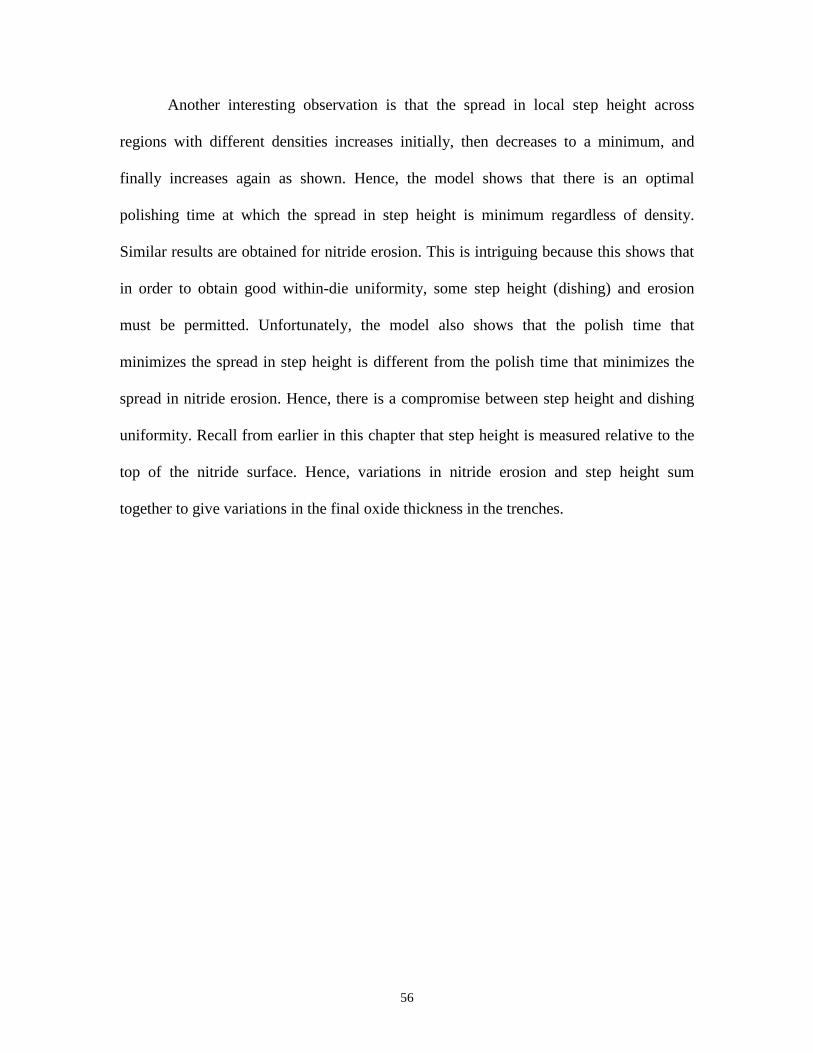
56
Another interesting observation is that the spread in local step height across
regions with different densities increases initially, then decreases to a minimum, and
finally increases again as shown. Hence, the model shows that there is an optimal
polishing time at which the spread in step height is minimum regardless of density.
Similar results are obtained for nitride erosion. This is intriguing because this shows that
in order to obtain good within-die uniformity, some step height (dishing) and erosion
must be permitted. Unfortunately, the model also shows that the polish time that
minimizes the spread in step height is different from the polish time that minimizes the
spread in nitride erosion. Hence, there is a compromise between step height and dishing
uniformity. Recall from earlier in this chapter that step height is measured relative to the
top of the nitride surface. Hence, variations in nitride erosion and step height sum
together to give variations in the final oxide thickness in the trenches.

57
0200
400−
2000
−1500
−1000
−500 0
500
1000
1500Step Height (Angstrom)
Process A
High D
ensity
Low D
ensity
0200
4000
500
1000
1500
2000
Polish T
ime (second)
Nitride Erosion (Angstrom)
Low D
ensity
High D
ensity
0200
400−
2000
−1500
−1000
−500 0
500
1000
1500P
rocess B
0200
4000
500
1000
1500
2000
Polish T
ime (second)
050
100150
−2000
−1500
−1000
−500 0
500
1000
1500P
rocess C
050
100150
0
500
1000
1500
2000
Polish T
ime (second)
Figure 3.9 Time evolution of step height and nitride erosion for a range of patterndensities. (Note: The horizontal scale for process C is different).
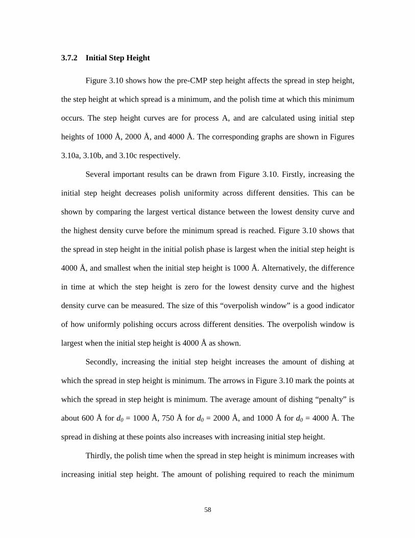
58
3.7.2 Initial Step Height
Figure 3.10 shows how the pre-CMP step height affects the spread in step height,
the step height at which spread is a minimum, and the polish time at which this minimum
occurs. The step height curves are for process A, and are calculated using initial step
heights of 1000 Å, 2000 Å, and 4000 Å. The corresponding graphs are shown in Figures
3.10a, 3.10b, and 3.10c respectively.
Several important results can be drawn from Figure 3.10. Firstly, increasing the
initial step height decreases polish uniformity across different densities. This can be
shown by comparing the largest vertical distance between the lowest density curve and
the highest density curve before the minimum spread is reached. Figure 3.10 shows that
the spread in step height in the initial polish phase is largest when the initial step height is
4000 Å, and smallest when the initial step height is 1000 Å. Alternatively, the difference
in time at which the step height is zero for the lowest density curve and the highest
density curve can be measured. The size of this “overpolish window” is a good indicator
of how uniformly polishing occurs across different densities. The overpolish window is
largest when the initial step height is 4000 Å as shown.
Secondly, increasing the initial step height increases the amount of dishing at
which the spread in step height is minimum. The arrows in Figure 3.10 mark the points at
which the spread in step height is minimum. The average amount of dishing “penalty” is
about 600 Å for d0 = 1000 Å, 750 Å for d0 = 2000 Å, and 1000 Å for d0 = 4000 Å. The
spread in dishing at these points also increases with increasing initial step height.
Thirdly, the polish time when the spread in step height is minimum increases with
increasing initial step height. The amount of polishing required to reach the minimum

59
spread in step height is about 150 s for d0 = 1000 Å, 200 s for d0 = 2000 Å, and 400 s for
d0 = 4000 Å.
Thus, the model shows that it is desirable to make the initial step height as small
as possible. Having a small initial step height decreases the spread in step height and
consequently the amount of overpolishing required. It also reduces the amount of dishing
“penalty” in order to obtain uniformity across a range of densities. Finally, it reduces the
polish time required to reach the minimum spread in step height.
0 500−2000
−1000
0
1000
2000
3000
4000
Ste
p H
eigh
t (A
ngst
rom
)
0 500−2000
−1000
0
1000
2000
3000
4000
Time (second)0 500
−2000
−1000
0
1000
2000
3000
4000
high density
low density
Figure 3.10 Effect of pre-CMP step height on post-CMP step height: (a) d0 = 1000 Å,(b) d0 = 2000 Å, (c) d0 = 4000 Å.
(a) (b) (c)

60
3.7.3 Oxide to Nitride Selectivity
Standard silica-based slurries commonly used in STI CMP today have oxide to
nitride selectivities that range from 2:1 to 5:1. To obtain high wafer throughput in
manufacturing, the amount of time spent polishing each wafer is reduced by increasing
the polish rate. As a result, the nitride removal rate is high, with values that range from a
few hundred to more than a thousand angstroms per minute, depending on the process
conditions used. The high nitride removal rate can cause significant nitride erosion to
occur, especially during overpolishing. This may in turn damage the silicon active area
underneath the nitride. Hence, high selectivity slurries are of great interest. In fact,
slurries with greater than 200:1 selectivity have been developed [25]. High selectivity to
nitride can be obtained by dramatically reducing the nitride removal rate to tens of
angstroms per minute while maintaining a high oxide removal rate.
Figure 3.11 shows the effect of selectivity on polish uniformity. The step height
and nitride erosion curves for process A are shown. Figure 3.11a is plotted using the
values of Kox and Knit in Table 3.2 (selectivity = 3.72:1). Figure 3.11b is plotted using the
same Kox but Knit = 0.01 × Kox (selectivity = 100:1).
Comparing the step height plots shows that increasing the oxide to nitride
selectivity improves polish uniformity by reducing the spread in step height and the size
of the overpolish window, and the polish time needed to reach the minimum spread in
step height. However, it increases the dishing “penalty”. The steady state dishing also
increases as expected since from equation (3.13):
( )d K Kss ox nit= −τ (3.13)

61
Comparing the nitride erosion plots shows that nitride erosion is reduced
dramatically as expected. Notice that the vertical scale for nitride erosion in Figure 3.11b
is larger.
In conclusion, the model predicts that using high selectivity slurries does improve
CMP performance by reducing the polish non-uniformity due to pattern density effects
and by reducing the amount of nitride erosion. However, excessive overpolishing can
result in more dishing than if lower selectivity slurry is used.
0 100 200 300 400−2000
−1000
0
1000
Ste
p H
eigh
t (A
ngst
rom
)
0 100 200 300 400−2000
−1000
0
1000
0 100 200 300 4000
500
1000
1500
2000
Nitr
ide
Ero
sion
(A
ngst
rom
)
Time (second)0 100 200 300 400
0
50
100
150
200
Time (second)
low density
high density
low density
high density
Figure 3.11 Effect of high selectivity slurry on step height and nitride erosion: (a)standard silica based slurry with 3.7:1 selectivity, (b) 100:1 selectivityslurry. Notice the larger scale for nitride erosion.
(a) (b)

62
Chapter 4Combined Planarization LengthParameter Extraction Methodology
In this chapter, a refinement to the parameter extraction methodology is
presented. The method described in the previous chapter used the designed pattern
densities in its calculations. However, we know from experience that the surface of a
post-CMP die is continuously varying and abrupt steps corresponding to abrupt changes
in final oxide thickness due to pattern density variations are not observed. We can infer
from this that during polishing, some averaging of the surrounding densities occurs, and
this density effect has been shown to be the primary effect in oxide inter-level dielectric
polishing [13]. Thus, we consider here an improvement in the extraction method by using
the effective density at each measurement point instead of the designed pattern density.
A method for calculating the average density due to CMP was described by Ouma
[21]. The updated extraction methodology described here integrates the average density
calculation with the basic extraction method described in Chapter 3. Section 4.1 briefly
reviews the concept of planarization length and how it can be used to calculate the
average density. Section 4.2 describes the updated parameter extraction methodology,
and the results are shown in Section 4.3.

63
4.1 Density Averaging using Planarization Length
CMP achieves planarization in two ways: (1) it removes topography by
selectively removing material from the up areas faster than the down areas; and (2) it
reduces step height variations by averaging the local density. Step height removal was
discussed using the removal rate-step height model in the previous chapter. In the
following discussion, we look at how we can model density averaging.
According to Ouma, the average density of any point on a wafer can be calculated
by taking the weighted average of the pattern densities inside a window centered at that
point [21]. The window size is determined by a single parameter known as the
planarization length. Physically, planarization length defines the length scale over which
planarity is achieved. This length scale is easily visualized by polishing a step density
pattern. As shown in Figure 4.1, away from the density boundary, uniform polishing
occurs at a removal rate given by the MIT density model. The oxide in the patterned
region polishes faster than the oxide in the unpatterned region. This introduces a step
height in the regions that are far away from the boundary. Close to the boundary, the
oxide thickness changes gradually from the patterned region to the unpatterned region.
The length of this transition region represents the planarization length.
Figure 4.1 Physical meaning of planarization length: (a) cross-section before CMP, (b)cross-section after CMP, showing the transition region near the step densityboundary.
planarization length
CMPoxide
silicon
(a) (b)

64
Once the planarization length is known, the effective density at any point on a
layout can be calculated. A weighting function is used to calculate the effective density
inside the averaging window. The optimal weighting function is an elliptic weighting
filter and it is shaped like the deformation profile of a polishing pad [21]. Figure 4.2
shows the effective density maps of the STI CMP characterization mask for different
planarization lengths. Figure 4.2a shows the top view of the die as it is patterned on the
wafers. Figures 4.2b and 4.2c show the effective density contour maps for planarization
lengths of 3.2 mm and 5.2 mm respectively. Clearly, a longer planarization length is more
effective at smoothing topography.
Figure 4.2 Density averaging: (a) layout of STI CMP characterization mask; (b)density map using 3.2 mm planarization length; (c) density map using 5.5mm planarization length.
(a)
(b)
(c)
PL = 3.2 mm
PL = 5.5 mm

65
Another way of visualizing how having a longer planarization length reduces
topography is to see how the distribution of effective density changes with planarization
length. Figure 4.3 shows the distribution of effective density on the STI CMP
characterization mask for three different planarization lengths. Figures 4.3a, 4.3b, and
4.3c show the histogram for planarization lengths of 3 mm, 5 mm, and 7 mm
respectively. The histograms show that increasing the planarization length reduces the
spread of effective densities and distributes the densities more evenly. These help to
improve polish uniformity as discussed in Chapter 3.
0 0.5 10
5
10
15x 10
4
Fre
quen
cy
0 0.5 10
5
10
15x 10
4
0 0.5 10
5
10
15x 10
4
Figure 4.3 Effective density distribution for planarization lengths of: (a) 3 mm, (b) 5mm, (c) 7 mm.
(a) (b) (c)
Effective Density

66
4.2 Improved Parameter Extraction Methodology
The improved parameter extraction methodology can be considered to be a
generalization of the basic method described in the previous chapter. If the planarization
length is chosen to be less than the length of each cell (3.5 mm) in the step density region,
the effective density ρi as measured from the center of each cell will be approximately the
designed pattern density and the results from the parameter extraction will be the same as
the results obtained in Table 3.2. Hence, the improved methodology allows processes of
any planarization length to be modeled.
Density averaging is done by convolving the averaging window and the layout.
To do this, the 21.095 mm × 21.095 mm layout is first discretized into 37 µm cells using
SiCat . The output is a 570 × 570 matrix (21.090 mm × 21.090 mm effective size),
where each element in the matrix represents the average density in a corresponding 37
µm × 37 µm area on the layout. In those locations where the length of the active area is
less than or equal to 1 µm, the corresponding location in the matrix is replaced with
zeros. This is because HDP oxide deposition is used during fabrication, which planarizes
these small features. In addition, reverse tone etch back is not performed on these
features, so the exposed nitride density is effectively zero.
Since the planarization lengths for processes A, B, and C are not known a priori,
they are chosen by optimizing the total sum-squared error given by a variant of equation
(3.16) for each process:
( ) ( )[ ] ( ) ( )[ ]arg min
, , ,PL K KH t h t E t e t
ox nit ii j i j i j i j
i
I
j
J
τ− + −
==∑∑
2 2
11
(4.1)

67
The optimization process is shown graphically in Figure 4.4. First, an arbitrary
value for planarization length (PL) is chosen. The planarization length determines the
size of the averaging window of the averaging function. An elliptical averaging function
is then used to calculate the effective density of the die (as seen by the polishing pad) by
convolving the elliptical function with the discretized die layout. The effective density for
each measurement site can then be found. Finally, using the measurements and the
effective densities, a multivariate optimization is performed to find Kox, Knit, and τ as per
the basic parameter extraction methodology. This process is repeated until the
planarization length that minimizes equation (4.1) is found.
Figure 4.4 Flow chart of updated parameter extraction methodology
Planarization LengthDiscretized Mask
LayoutLocation of
Measurement Sites
Kox, Knit, τ Calculate SSE
Calculate EffectiveDensity
Minimum?
Minimum?
EndNo Yes
No
Yes
Basic ParameterExtraction Methodology
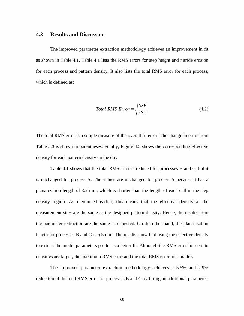
68
4.3 Results and Discussion
The improved parameter extraction methodology achieves an improvement in fit
as shown in Table 4.1. Table 4.1 lists the RMS errors for step height and nitride erosion
for each process and pattern density. It also lists the total RMS error for each process,
which is defined as:
Total RMS ErrorSSE
i j=
× (4.2)
The total RMS error is a simple measure of the overall fit error. The change in error from
Table 3.3 is shown in parentheses. Finally, Figure 4.5 shows the corresponding effective
density for each pattern density on the die.
Table 4.1 shows that the total RMS error is reduced for processes B and C, but it
is unchanged for process A. The values are unchanged for process A because it has a
planarization length of 3.2 mm, which is shorter than the length of each cell in the step
density region. As mentioned earlier, this means that the effective density at the
measurement sites are the same as the designed pattern density. Hence, the results from
the parameter extraction are the same as expected. On the other hand, the planarization
length for processes B and C is 5.5 mm. The results show that using the effective density
to extract the model parameters produces a better fit. Although the RMS error for certain
densities are larger, the maximum RMS error and the total RMS error are smaller.
The improved parameter extraction methodology achieves a 5.5% and 2.9%
reduction of the total RMS error for processes B and C by fitting an additional parameter,
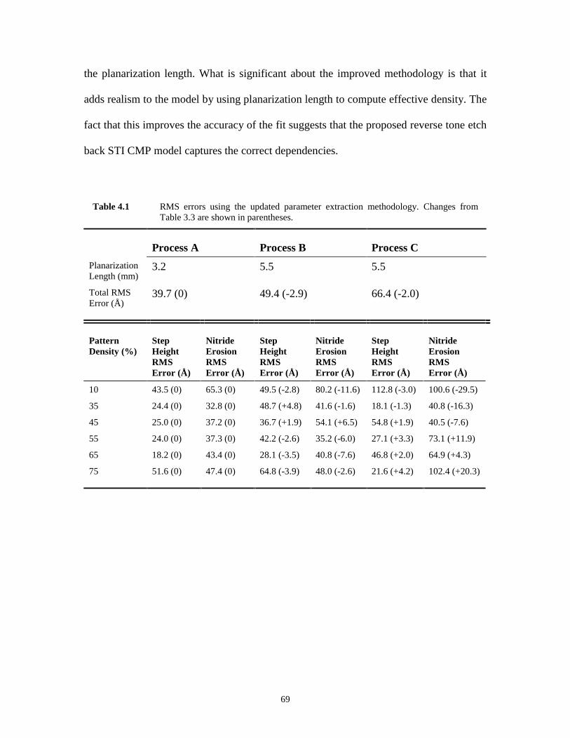
69
the planarization length. What is significant about the improved methodology is that it
adds realism to the model by using planarization length to compute effective density. The
fact that this improves the accuracy of the fit suggests that the proposed reverse tone etch
back STI CMP model captures the correct dependencies.
Table 4.1 RMS errors using the updated parameter extraction methodology. Changes fromTable 3.3 are shown in parentheses.
Process A Process B Process C
PlanarizationLength (mm)
3.2 5.5 5.5
Total RMSError (Å)
39.7 (0) 49.4 (-2.9) 66.4 (-2.0)
PatternDensity (%)
StepHeightRMSError (Å)
NitrideErosionRMSError (Å)
StepHeightRMSError (Å)
NitrideErosionRMSError (Å)
StepHeightRMSError (Å)
NitrideErosionRMSError (Å)
10 43.5 (0) 65.3 (0) 49.5 (-2.8) 80.2 (-11.6) 112.8 (-3.0) 100.6 (-29.5)
35 24.4 (0) 32.8 (0) 48.7 (+4.8) 41.6 (-1.6) 18.1 (-1.3) 40.8 (-16.3)
45 25.0 (0) 37.2 (0) 36.7 (+1.9) 54.1 (+6.5) 54.8 (+1.9) 40.5 (-7.6)
55 24.0 (0) 37.3 (0) 42.2 (-2.6) 35.2 (-6.0) 27.1 (+3.3) 73.1 (+11.9)
65 18.2 (0) 43.4 (0) 28.1 (-3.5) 40.8 (-7.6) 46.8 (+2.0) 64.9 (+4.3)
75 51.6 (0) 47.4 (0) 64.8 (-3.9) 48.0 (-2.6) 21.6 (+4.2) 102.4 (+20.3)

70
0 10 20 30 40 50 60 70 80 90 1000
10
20
30
40
50
60
70
80
90
100
Pattern Density (%)
Effe
ctiv
e D
ensi
ty (
%)
DesignedProcess AProcesses B and C
Density (%)
Designed 10.0 35.0 45.0 55.0 65.0 75.0
Process A (PL = 3.2 mm) 9.9 35.0 45.1 54.9 65.0 75.1
Process B, C (PL = 5.5 mm) 18.6 42.9 49.2 45.4 57.1 55.6
Figure 4.5 Effective density vs. pattern density

71
Chapter 5Conclusion and Future Work
This work has examined chemical mechanical polishing for shallow trench
isolation, in particular, shallow trench isolation fabrication using the reverse tone etch
back technique. The main contribution of this work is reverse tone etch back STI CMP
modeling, beginning with an introduction to device isolation in Chapter 1, which
provided motivation for device isolation, and presented two common isolation
techniques: LOCOS and STI. Chapter 2 introduced CMP as an enabling technique for
STI formation, highlighted some of the problems encountered during STI CMP, and
presented the reverse tone etch back technique as a solution to some of these problems. A
removal rate vs. step height model for reverse tone etch back STI CMP was developed in
Chapter 3, and further extended to incorporate density averaging effects in Chapter 4.
This chapter concludes this work with a summary of the main results from this study and
a presentation of some model applications. Areas for future work are also identified.
5.1 STI CMP Modeling
A reverse tone etch back STI CMP model incorporating density averaging effects
was developed and validated using experimental data. The model confirms that die-level
density variations cause polish non-uniformity. Hence, more uniform polishing can be
achieved by using processes with longer planarization lengths to reduce the effective
density spread. Polish uniformity can be further improved by reducing the pre-CMP step

72
height and by using slurries with high oxide to nitride selectivity. Furthermore, the model
predicts that the density effects on polish uniformity can be almost completely eliminated
by slightly overpolishing the wafers. Although some dishing occurs as a result of
overpolishing, almost constant dishing across a range of densities can be achieved. The
contribution of nitride erosion variations to post-CMP non-uniformity is small, especially
when high selectivity slurries are used. In addition, it was shown that having a smaller
initial step height also improves polish uniformity.
5.2 Applications of the Methodology
Accurate film thickness prediction during CMP is useful for many applications.
The results from the modeling can be used for process improvement and optimization.
One such application is to determine the optimal film thickness that must be deposited for
any given planarization requirement. The model can also be used to rapidly characterize
existing and new processes. These results can be used to predict the optimum process
conditions. This reduces the amount of guess work needed to optimize the CMP process,
which shortens process development time and reduces consumable waste. These time and
cost savings can be substantial for a typical manufacturing plant.

73
5.3 Future Work
A method for characterizing CMP processes using the STI CMP characterization
mask was described and demonstrated. Total RMS errors of less than 100 Å were
obtained. However, additional work is still needed to further validate the model and
answer some unexpected results.
5.3.1 Validation on Non-Standard Structures
The STI structures that are used for this study are square patterns with 80µm pitch
which are meant to emulate isolated active areas. The current model says that for any
given process, the post-CMP step height and nitride erosion depends only on the initial
step height, and the effective density. Future experiments should investigate if the shape
and size of the active area affects step height and erosion. A more comprehensive
characterization mask might include active areas of different shapes and sizes, as well as
structures with constant density/varying pitch and constant pitch/varying density. In
addition, the model was applied to relatively large active areas and trench (smallest active
area length = 25.3 µm); further work is needed to measure, analyze, and potentially
extend the model for very small features where polish may be accelerated.
5.3.2 Process Variations
The results for wafers with different starting step heights and processes using
high selectivity slurries were predicted using the proposed model and the extracted model
parameters. These predictions should be verified in future experiments.

74
5.3.3 Steady-State Dishing (dss) and Pad Deformation Limit (dmax)
Some guess work can be eliminated from the model by running controlled
experiments to experimentally determine dss or dmax. For example, dss can be found by
severely overpolishing STI wafers with a thick (>1µm) nitride layer until steady-state
dishing is achieved. Likewise, dmax can be found by carefully polishing of STI wafers
with large (> 5000 Å) initial step heights in small time increments.
5.3.4 Kox and Knit
The extracted values for Kox and Knit are smaller than the removal rates obtained
by polishing blanket oxide and nitride wafers respectively. In addition, the oxide to
nitride selectivity obtained using the parameter extraction methodology is higher than
expected. Some additional modeling work is needed to explain these differences in
results.
Table 5.1 Expected and extracted values for Kox, Knit, and selectivity
Process A Process B Process C
Blanket Oxide RR (Å/min) 1031 938 2179
Kox (Å/min) 848 771 2189
Blanket Nitride RR (Å/min) — — 783
Knit (Å/min) 228 207 628
Measured Selectivity 2.44 1 2.44 2 2.78
Extracted Selectivity 3.72 3.72 3.49
1 value obtained from previous characterization experiments2 estimated value, assuming the effect of pad type on selectivity is small

75
Bibliography
[1] M. Nandakumar, A. Chatterjee, S. Sridhar, K. Joyner, M. Rodder, and I.-C. Chen,“Shallow Trench Isolation for Advanced ULSI CMOS Technologies,”International Electron Devices Meeting, IEDM ’98 Technical Digest, pp. 133-136, 1998.
[2] A. Chatterjee, J. Esquivel, S. Nag, I. Ali, D. Rogers, K. Taylor, K. Joyner, M.Mason, D. Mercer, A. Amerasekera, T. Houston, and I.-C. Chen, “A ShallowTrench Isolation Study for 0.25/0.18um CMOS Technologies and Beyond,” 1996Symposium on VLSI Technology, Digest of Technical Papers, pp. 156-157, 1996.
[3] Andres Bryant, Wilfried Hänsch, and Toshio Mii, “Characteristics of CMOSDevice Isolation for the ULSI Age,” International Electron Devices Meeting,Technical Digest, pp. 671-674, 1994.
[4] International Technology Roadmap for Semiconductors, 1999.
[5] S. M. Sze, VLSI Technology, McGraw-Hill, 1988.
[6] J. Song, “Process Capability of Local Oxidation of Silicon Isolation Technologyfor Sub-Half Micrometre Custom IC Applications,” Electronics Letters, Vol. 35,No. 6, pp. 505-506, 18 March 1999.
[7] Stephen A. Campbell, The Science and Engineering of MicroelectronicFabrication, Oxford University Press, 1996.
[8] C. Y. Chang, S. M. Sze, ULSI Technology, McGraw-Hill, 1996.
[9] John O. Borland and H. T. Cho, “LOCOS-vs.-Shallow Trench Isolation Latch-upUsing MeV Implantation for Well Formation Down to 0.18um Design Rules,”1998 International Conference on Ion Implantation Technology Proceedings,Vol. 1, pp. 67-70, 1999.
[10] Pierre C. Fazan and Viju K. Mathews, “A Highly Manufacturable TrenchIsolation Process for Deep Submicron DRAMs,” International Electron DevicesMeeting, Technical Digest, pp. 57-60, 1993.
[11] Hung-Wen Chiou and Lai-Juh Chen, “One Step Effective Planarization ofShallow Trench Isolation,” Proceedings of the IEEE 1998 InternationalInterconnect Technology Conference, pp. 199-201, 1998.
[12] N. Elbel, Z. Gabric, W. Langheinrich, and B. Neureither, “A New STI ProcessBased on Selective Oxide Deposition,” 1998 Symposium on VLSI Technology,Digest of Technical Papers, pp. 208-209, 1998.
76
[13] B. E. Stine, D. O. Ouma, R. R. Divecha, D. S. Boning, J. E. Chung, D. L.Hetherington, C. R. Harwood, O. S. Nakagawa, and S.-Y. Oh, “RapidCharacterization and Modeling of Pattern-Dependent Variation in Chemical-Mechanical Polishing,” IEEE Transactions on Semiconductor Manufacturing,Vol. 11, No. 1, pp. 129-140, February 1998.
[14] B. Davari, C. W. Koburger, R. Schulz, J. D. Warnock, T. Furukawa, M. Jost, Y.Taur, W. G. Scheittek, J. K. DeBrosse, M. L. Kerbaugh, and J. L. Mauer, “A NewPlanarization Technique, Using a Combination of RIE and Chemical MechanicalPolishing (CMP),” International Electron Devices Meeting, Technical Digest, pp.61-64, 1989.
[15] Y. Wu, J. Gilhooly, and B. Philips, “Control Methods for the Chemical-Mechanical Polishing Process in Shallow Trench Isolation,” 1998 IEEE/SEMIAdvanced Semiconductor Manufacturing Conference & Workshop, pp. 66-70,1998.
[16] T. Tugbawa, T. Park, D. Boning, T. Pan, P. Li, S. Hymes, T. Brown, and L.Camilletti, “A Mathematical Model of Pattern Dependencies in Cu CMPProcesses,” CMP Symposium, Electrochemical Society Meeting, Honolulu, HA,October 1999.
[17] B. Lee, D. S. Boning, D. L. Hetherington, and D. J. Stein, “Using Smart DummyFill and Selective Reverse Etchback for Pattern Density Equalization,” ChemicalMechanical Polish for ULSI Multilevel Interconnection Conference (CMP-MIC),pp. 255-258, Santa Clara, March 2000.
[18] E. P. Giannelis and Y. Y. Shacham-Diamand, “Spin-On Films Add NewDimension to ULSI Circuits,” IEEE Circuits and Devices Magazine, Vol. 9, No.6, pp. 30-34, November 1993.
[19] B. Stine, D. Ouma, R. Divecha, D. Boning, J. Chung, D. L. Hetherington, I. Ali,G. Shinn, J. Clark, O. S. Nakagawa, and S.-Y. Oh, “A Closed-Form AnalyticModel for ILD Thickness Variation in CMP Processes,” 1997 ChemicalMechanical Polish for ULSI Multilevel Interconnection Conference (CMP-MIC),pp. 266, Santa Clara, February 1997.
[20] T. H. Smith, S. J. Fang, D. S. Boning, G. B. Shinn, and J. A. Stefani, “A CMPModel Combining Density and Time Dependencies,” 1999 Chemical MechanicalPolish for ULSI Multilevel Interconnection Conference (CMP-MIC), Santa Clara,February 1999.
[21] Dennis Okumu Ouma, “Modeling of Chemical Mechanical Polishing forDielectric Planarization,” Ph.D. Thesis, Massachusetts Institute of Technology,1998.

77
[22] J. Grillaert, M. Meuris, N. Heyley, K. Devriendt, E. Vrancken, and M. Heyns,“Modeling Step Height Reduction and Local Removal Rates Based on Pad-Substrate Interactions,” 1998 Chemical Mechanical Polish for ULSI MultilevelInterconnection Conference (CMP-MIC), pp.79-86, Santa Clara, February 1998.
[23] Peter A. Burke, “Semi-Empirical Modeling of SiO2 Chemical-MechanicalPolishing Planarization,” 1991 VMIC Conference, pp. 379-384, June 11-12 1991.
[24] E. Tseng, C. Yi, and H. C. Chen, “A Mechanical Model for DRAM DielectricChemical-Mechanical Polishing Process,” 1997 Chemical Mechanical Polish forULSI Multilevel Interconnection Conference (CMP-MIC), pp. 258-265, SantaClara, February 1997.
[25] S. D. Hosali, A. R. Sethuraman, J.-F. Wang, L. M. Cook, and D. R. Evans,“Planarization Process and Consumable Development for Shallow TrenchIsolation,” 1997 Chemical Mechanical Polish for ULSI Multilevel InterconnectionConference (CMP-MIC), pp. 52-57, Santa Clara, February 1997.

78
Appendix A-1Planarization Length Optimization for Process A
% Created March 29, 2000. Terence Gan.% Run this to optimize PL and parameters for process A.
x = [4000]; % initial estimate for planarization length
options = optimset(’fminsearch’);options.TolFun = 1;options.TolX = 1;options.MaxFunEvals = 100000;options.MaxIter = 100000;
xOpt = fminsearch(’pla_exe2’, x,options,dmask,pl_xy,37);
% variable declarations --------------------------------
global den % effective densityglobal Kox % oxide removal rateglobal Knit % nitride removal rateglobal total_rms % total RMS errorglobal tau % exponential time constantglobal dss % steady state dishingglobal Hrms % step height rms errorsglobal Erms % nitride erosion rms errors
% display summary of results ---------------------------
pl = xOptKoxKnittotal_rmsdentaudssdmax = tau.*((1-den)*Knit+den*Kox)./(1-den)HrmsErms

79
Appendix A-2Density and Parameter Extraction for Process A
function [cost] = pla_exe2(pl,dmask,pl_xy,cell_length)
% Created March 29, 2000. Terence Gan.% This is the first inner optimization loop, it is the% cost function for optimizing the planarization length.% It uses the input planarization length to extract the% effective density at each of the measurement points.
% pl = planarization length (um)% dmask = discretized mask layout% pl_xy = xy-coordinates of measurement points (um)% cell_length = level of discretization in dmask (um)
% get effective density
global denden = pl_get_density(dmask,pl_xy,pl,cell_length);
% minimize sum-squared error between model and data% using another optimization loop
x = [800 200 5 5 5 5 5 5];options = optimset(’fminsearch’);options.TolFun = 1e-3;options.TolX = 1e-3;options.MaxFunEvals = 100000;options.MaxIter = 100000;xOpt = fminsearch(’pla_exe3’, x,options,den);
% display planarization length with each iteration
pl
% display total_rms with each iteration
global total_rmstotal_rms
% use the same cost from the plb_exe3 loop
global cost

80
Appendix A-3Cost Function for Process A
function [cost] = pla_exe3(x,den)
% Created March 29, 2000. Terence Gan.% This is the second inner optimization loop, it is the% cost function for optimizing Kox, Knit, and tau by% minimizing the sum-squared error between the model and% the measurement data.
% x = vector containing Kox, Knit, and tau% den = vector of effective density
% step height measurements
h10 = [ 319 104 -155 -337 -781 -980 -1087];h35 = [ 192 13 -217 -423 -810 -1003 -1070];h45 = [ 117 -70 -287 -480 -835 -1005 -1061];h55 = [ 81 -141 -280 -481 -797 -922 -1005];h65 = [ -32 -206 -364 -526 -771 -892 -934];h75 = [-104 -210 -348 -451 -649 -732 -779];
% nitride erosion measurements
e10 = [ 283 314 426 479 757 942 1013];e35 = [ 339 365 464 528 748 881 916];e45 = [ 342 377 466 525 737 859 904];e55 = [ 353 398 488 547 758 868 922];e65 = [ 354 396 491 563 755 859 897];e75 = [ 368 406 509 564 756 875 913];
% initial step height measurements (pre-CMP)
d10 = [1313 1596 1292 1629 1437 1414 1690];d35 = [1313 1595 1292 1630 1438 1415 1690];d45 = [1321 1597 1298 1633 1446 1424 1697];d55 = [1312 1597 1291 1629 1436 1413 1692];d65 = [1321 1597 1297 1631 1445 1423 1695];d75 = [1314 1595 1293 1629 1439 1415 1689];
% polish time
t = [ 90 124 127 168 211 230 253];
% variable declaration
global costglobal Koxglobal Knitglobal total_rmsglobal tauglobal dssglobal Hrms

81
global Erms
Kox = x(1);Knit = x(2);
tau(1) = x(3);tau(2) = x(4);tau(3) = x(5);tau(4) = x(6);tau(5) = x(7);tau(6) = x(8);
% calculating step height and nitride erosion using the model
dss = (Kox-Knit)*tau;
for i = 1:length(t),
H10(i) = -(dss(1)+d10(i))*(1-exp(-t(i)/60/tau(1)))+d10(i); E10(i) = (Kox*Knit*t(i)/60 - ...
Knit*(1-den(1))*(dss(1)+d10(i))*(1-exp(-t(i)/60/tau(1))))/... ((1-den(1))*Knit+den(1)*Kox);
H35(i) = -(dss(2)+d35(i))*(1-exp(-t(i)/60/tau(2)))+d35(i); E35(i) = (Kox*Knit*t(i)/60 - ...
Knit*(1-den(2))*(dss(2)+d35(i))*(1-exp(-t(i)/60/tau(2))))/... ((1-den(2))*Knit+den(2)*Kox);
H45(i) = -(dss(3)+d45(i))*(1-exp(-t(i)/60/tau(3)))+d45(i); E45(i) = (Kox*Knit*t(i)/60 - ...
Knit*(1-den(3))*(dss(3)+d45(i))*(1-exp(-t(i)/60/tau(3))))/... ((1-den(3))*Knit+den(3)*Kox);
H55(i) = -(dss(4)+d55(i))*(1-exp(-t(i)/60/tau(4)))+d55(i); E55(i) = (Kox*Knit*t(i)/60 - ...
Knit*(1-den(4))*(dss(4)+d55(i))*(1-exp(-t(i)/60/tau(4))))/... ((1-den(4))*Knit+den(4)*Kox);
H65(i) = -(dss(5)+d65(i))*(1-exp(-t(i)/60/tau(5)))+d65(i); E65(i) = (Kox*Knit*t(i)/60 - ...
Knit*(1-den(5))*(dss(5)+d65(i))*(1-exp(-t(i)/60/tau(5))))/... ((1-den(5))*Knit+den(5)*Kox);
H75(i) = -(dss(6)+d75(i))*(1-exp(-t(i)/60/tau(6)))+d75(i); E75(i) = (Kox*Knit*t(i)/60 - ...
Knit*(1-den(6))*(dss(6)+d75(i))*(1-exp(-t(i)/60/tau(6))))/... ((1-den(6))*Knit+den(6)*Kox);
end
% This calculates the sum-squared errors% fminsearch tries to minimize the cost
Herr10 = H10-h10;Herr35 = H35-h35;Herr45 = H45-h45;Herr55 = H55-h55;

82
Herr65 = H65-h65;Herr75 = H75-h75;
Eerr10 = E10-e10;Eerr35 = E35-e35;Eerr45 = E45-e45;Eerr55 = E55-e55;Eerr65 = E65-e65;Eerr75 = E75-e75;
error = [Herr10 Herr35 Herr45 Herr55 Herr65 Herr75 ... Eerr10 Eerr35 Eerr45 Eerr55 Eerr65 Eerr75 ];
cost = error*error’;total_rms = sqrt(cost/length(error));
Hrms10 = sqrt(Herr10*Herr10’/length(Herr10));Hrms35 = sqrt(Herr35*Herr35’/length(Herr35));Hrms45 = sqrt(Herr45*Herr45’/length(Herr45));Hrms55 = sqrt(Herr55*Herr55’/length(Herr55));Hrms65 = sqrt(Herr65*Herr65’/length(Herr65));Hrms75 = sqrt(Herr75*Herr75’/length(Herr75));
Erms10 = sqrt(Eerr10*Eerr10’/length(Eerr10));Erms35 = sqrt(Eerr35*Eerr35’/length(Eerr35));Erms45 = sqrt(Eerr45*Eerr45’/length(Eerr45));Erms55 = sqrt(Eerr55*Eerr55’/length(Eerr55));Erms65 = sqrt(Eerr65*Eerr65’/length(Eerr65));Erms75 = sqrt(Eerr75*Eerr75’/length(Eerr75));
Hrms = [Hrms10 Hrms35 Hrms45 Hrms55 Hrms65 Hrms75];Erms = [Erms10 Erms35 Erms45 Erms55 Erms65 Erms75];

83
Appendix B-1Planarization Length Optimization for Process B
% Created March 29, 2000. Terence Gan.% Run this to optimize PL and parameters for process B.
x = [4000]; % initial estimate for planarization length
options = optimset(’fminsearch’);options.TolFun = 1;options.TolX = 1;options.MaxFunEvals = 100000;options.MaxIter = 100000;
xOpt = fminsearch(’plb_exe2’, x,options,dmask,pl_xy,37);
% variable declarations ---------------------------------
global den % effective densityglobal Kox % oxide removal rateglobal Knit % nitride removal rateglobal total_rms % total RMS errorglobal tau % exponential time constantglobal dss % steady state dishingglobal Hrms % step height rms errorsglobal Erms % nitride erosion rms errors
% summary of results ------------------------------------
pl = xOptKoxKnittotal_rmsdentaudssdmax = tau.*((1-den)*Knit+den*Kox)./(1-den)HrmsErms

84
Appendix B-2Density and Parameter Extraction for Process B
function [cost] = plb_exe2(pl,dmask,pl_xy,cell_length)
% Created March 29, 2000. Terence Gan.% This is the first inner optimization loop, it is the% cost function for optimizing the planarization length.% It uses the input planarization length to extract the% effective density at each of the measurement points.
% pl = planarization length (um)% dmask = discretized mask layout% pl_xy = xy-coordinates of measurement points (um)% cell_length = level of discretization in dmask (um)
% get effective density
global denden = pl_get_density(dmask,pl_xy,pl,cell_length);
% optimize sum-squared error between model and data% using another optimization loop
x = [800 200 5 5 5 5 5 5];options = optimset(’fminsearch’);options.TolFun = 1e-3;options.TolX = 1e-3;options.MaxFunEvals = 100000;options.MaxIter = 100000;xOpt = fminsearch(’plb_exe3’, x,options,den);
% display planarization length with each iteration
pl
% display total_rms with each iteration
global total_rmstotal_rms
% use the same cost from the plb_exe3 loop
global cost

85
Appendix B-3Cost Function for Process B
function [cost] = plb_exe3(x,den)
% Created March 29, 2000. Terence Gan.% This is the second inner optimization loop, it is the% cost function for optimizing Kox, Knit, and tau by% minimizing the sum-squared error between the model and% the measurement data.
% x = vector containing Kox, Knit, and tau% den = vector of effective density
% step height measurements
h10 = [357 160 -18 -259 -694 -925 -987];h35 = [272 122 -115 -306 -742 -946 -1027];h45 = [224 79 -83 -261 -693 -904 -999];h55 = [185 -31 -123 -302 -705 -842 -919];h65 = [ 91 -61 -207 -350 -679 -815 -891];h75 = [ 7 -108 -239 -366 -587 -691 -728];
% nitride erosion measurements
e10 = [ 261 256 364 430 658 909 1006];e35 = [ 299 287 407 451 674 861 923];e45 = [ 291 284 377 425 614 801 882];e55 = [ 308 311 402 445 659 825 871];e65 = [ 302 299 404 453 650 811 887];e75 = [ 320 312 425 487 670 861 884];
% initial step height measurements (pre-CMP)
d10 = [1393 1620 1338 1601 1677 1400 1692];d35 = [1395 1621 1340 1599 1677 1402 1692];d45 = [1404 1628 1347 1601 1680 1411 1696];d55 = [1392 1621 1337 1602 1677 1399 1693];d65 = [1402 1626 1346 1601 1679 1410 1695];d75 = [1395 1620 1340 1600 1677 1402 1690];
% polish time
t = [ 94 125 132 167 220 235 270];
% variable declaration
global costglobal Koxglobal Knitglobal total_rmsglobal tauglobal dssglobal Hrms

86
global Erms
Kox = x(1);Knit = x(2);
tau(1) = x(3);tau(2) = x(4);tau(3) = x(5);tau(4) = x(6);tau(5) = x(7);tau(6) = x(8);
% calculating step height and nitride erosion using the model
dss = (Kox-Knit)*tau;
for i = 1:length(t),
H10(i) = -(dss(1)+d10(i))*(1-exp(-t(i)/60/tau(1)))+d10(i); E10(i) = (Kox*Knit*t(i)/60 - ...
Knit*(1-den(1))*(dss(1)+d10(i))*(1-exp(-t(i)/60/tau(1))))/... ((1-den(1))*Knit+den(1)*Kox);
H35(i) = -(dss(2)+d35(i))*(1-exp(-t(i)/60/tau(2)))+d35(i); E35(i) = (Kox*Knit*t(i)/60 - ...
Knit*(1-den(2))*(dss(2)+d35(i))*(1-exp(-t(i)/60/tau(2))))/... ((1-den(2))*Knit+den(2)*Kox);
H45(i) = -(dss(3)+d45(i))*(1-exp(-t(i)/60/tau(3)))+d45(i); E45(i) = (Kox*Knit*t(i)/60 - ...
Knit*(1-den(3))*(dss(3)+d45(i))*(1-exp(-t(i)/60/tau(3))))/... ((1-den(3))*Knit+den(3)*Kox);
H55(i) = -(dss(4)+d55(i))*(1-exp(-t(i)/60/tau(4)))+d55(i); E55(i) = (Kox*Knit*t(i)/60 - ...
Knit*(1-den(4))*(dss(4)+d55(i))*(1-exp(-t(i)/60/tau(4))))/... ((1-den(4))*Knit+den(4)*Kox);
H65(i) = -(dss(5)+d65(i))*(1-exp(-t(i)/60/tau(5)))+d65(i); E65(i) = (Kox*Knit*t(i)/60 - ...
Knit*(1-den(5))*(dss(5)+d65(i))*(1-exp(-t(i)/60/tau(5))))/... ((1-den(5))*Knit+den(5)*Kox);
H75(i) = -(dss(6)+d75(i))*(1-exp(-t(i)/60/tau(6)))+d75(i); E75(i) = (Kox*Knit*t(i)/60 - ...
Knit*(1-den(6))*(dss(6)+d75(i))*(1-exp(-t(i)/60/tau(6))))/... ((1-den(6))*Knit+den(6)*Kox);
end
% This calculates the sum-squared errors% fminsearch tries to minimize the cost
Herr10 = H10-h10;Herr35 = H35-h35;Herr45 = H45-h45;Herr55 = H55-h55;

87
Herr65 = H65-h65;Herr75 = H75-h75;
Eerr10 = E10-e10;Eerr35 = E35-e35;Eerr45 = E45-e45;Eerr55 = E55-e55;Eerr65 = E65-e65;Eerr75 = E75-e75;
error = [Herr10 Herr35 Herr45 Herr55 Herr65 Herr75 ... Eerr10 Eerr35 Eerr45 Eerr55 Eerr65 Eerr75 ];
cost = error*error’;total_rms = sqrt(cost/length(error));
Hrms10 = sqrt(Herr10*Herr10’/length(Herr10));Hrms35 = sqrt(Herr35*Herr35’/length(Herr35));Hrms45 = sqrt(Herr45*Herr45’/length(Herr45));Hrms55 = sqrt(Herr55*Herr55’/length(Herr55));Hrms65 = sqrt(Herr65*Herr65’/length(Herr65));Hrms75 = sqrt(Herr75*Herr75’/length(Herr75));
Erms10 = sqrt(Eerr10*Eerr10’/length(Eerr10));Erms35 = sqrt(Eerr35*Eerr35’/length(Eerr35));Erms45 = sqrt(Eerr45*Eerr45’/length(Eerr45));Erms55 = sqrt(Eerr55*Eerr55’/length(Eerr55));Erms65 = sqrt(Eerr65*Eerr65’/length(Eerr65));Erms75 = sqrt(Eerr75*Eerr75’/length(Eerr75));
Hrms = [Hrms10 Hrms35 Hrms45 Hrms55 Hrms65 Hrms75];Erms = [Erms10 Erms35 Erms45 Erms55 Erms65 Erms75];

88
Appendix C-1Planarization Length Optimization for Process C
% Created March 29, 2000. Terence Gan.% Run this to optimize PL and parameters for process C.
x = [4000]; % initial estimate for planarization length
options = optimset(’fminsearch’);options.TolFun = 1;options.TolX = 1;options.MaxFunEvals = 100000;options.MaxIter = 100000;
xOpt = fminsearch(’plc_exe2’, x,options,dmask,pl_xy,37);
% variable declarations --------------------------------
global den % effective densityglobal Kox % oxide removal rateglobal Knit % nitride removal rateglobal total_rms % total RMS errorglobal tau % exponential time constantglobal dss % steady state dishingglobal Hrms % step height rms errorsglobal Erms % nitride erosion rms errors
% summary of results -----------------------------------
pl = xOptKoxKnittotal_rmsdentaudssdmax = tau.*((1-den)*Knit+den*Kox)./(1-den)HrmsErms

89
Appendix C-2Density and Parameter Extraction for Process C
function [cost] = plc_exe2(pl,dmask,pl_xy,cell_length)
% Created March 29, 2000. Terence Gan.% This is the first inner optimization loop, it is the% cost function for optimizing the planarization length.% It uses the input planarization length to extract the% effective density at each of the measurement points.
% pl = planarization length (um)% dmask = discretized mask layout% pl_xy = xy-coordinates of measurement points (um)% cell_length = level of discretization in dmask (um)
% get effective density
global denden = pl_get_density(dmask,pl_xy,pl,cell_length);
% optimize sum-squared error between model and data% using another optimization loop
x = [2000 600 1 1 1 1 1 1];options = optimset(’fminsearch’);options.TolFun = 1e-3;options.TolX = 1e-3;options.MaxFunEvals = 100000;options.MaxIter = 100000;xOpt = fminsearch(’plc_exe3’, x,options,den);
% display planarization length with each iteration
pl
% display total_rms with each iteration
global total_rmstotal_rms
% use the same cost from the plb_exe3 loop
global cost

90
Appendix C-3Cost Function for Process C
function [cost] = plc_exe3(x,den)
% Created March 29, 2000. Terence Gan.% This is the second inner optimization loop, it is the% cost function for optimizing Kox, Knit, and tau by% minimizing the sum-squared error between the model and% the measurement data.
% x = vector containing Kox, Knit, and tau% den = vector of effective density
% step height measurements
h10 = [-114 -189 -574 -636 -860];h35 = [-290 -357 -641 -705 -787];h45 = [-348 -434 -676 -728 -803];h55 = [-336 -405 -606 -650 -720];h65 = [-377 -445 -618 -642 -704];h75 = [-321 -378 -515 -512 -561];
% nitride erosion measurements
e10 = [ 353 334 762 1012 1026];e35 = [ 416 417 748 889 986];e45 = [ 432 446 739 876 953];e55 = [ 461 459 713 855 914];e65 = [ 467 479 716 823 919];e75 = [ 489 497 729 813 873];
% initial step height measurements (pre-CMP)
d10 = [1347 1628 1348 1398 1633];d35 = [1351 1628 1350 1400 1634];d45 = [1358 1627 1356 1406 1636];d55 = [1345 1630 1347 1397 1633];d65 = [1356 1626 1356 1406 1634];d75 = [1349 1625 1350 1400 1633];
% polish time
t = [ 46 54 70 85 95];
% variable declaration
global costglobal Koxglobal Knitglobal total_rmsglobal tauglobal dssglobal Hrms

91
global Erms
Kox = x(1);Knit = x(2);
tau(1) = x(3);tau(2) = x(4);tau(3) = x(5);tau(4) = x(6);tau(5) = x(7);tau(6) = x(8);
% calculating step height and nitride erosion using the model
dss = (Kox-Knit)*tau;
for i = 1:length(t),
H10(i) = -(dss(1)+d10(i))*(1-exp(-t(i)/60/tau(1)))+d10(i); E10(i) = (Kox*Knit*t(i)/60 - ...
Knit*(1-den(1))*(dss(1)+d10(i))*(1-exp(-t(i)/60/tau(1))))/... ((1-den(1))*Knit+den(1)*Kox);
H35(i) = -(dss(2)+d35(i))*(1-exp(-t(i)/60/tau(2)))+d35(i); E35(i) = (Kox*Knit*t(i)/60 - ...
Knit*(1-den(2))*(dss(2)+d35(i))*(1-exp(-t(i)/60/tau(2))))/... ((1-den(2))*Knit+den(2)*Kox);
H45(i) = -(dss(3)+d45(i))*(1-exp(-t(i)/60/tau(3)))+d45(i); E45(i) = (Kox*Knit*t(i)/60 - ...
Knit*(1-den(3))*(dss(3)+d45(i))*(1-exp(-t(i)/60/tau(3))))/... ((1-den(3))*Knit+den(3)*Kox);
H55(i) = -(dss(4)+d55(i))*(1-exp(-t(i)/60/tau(4)))+d55(i); E55(i) = (Kox*Knit*t(i)/60 - ...
Knit*(1-den(4))*(dss(4)+d55(i))*(1-exp(-t(i)/60/tau(4))))/... ((1-den(4))*Knit+den(4)*Kox);
H65(i) = -(dss(5)+d65(i))*(1-exp(-t(i)/60/tau(5)))+d65(i); E65(i) = (Kox*Knit*t(i)/60 - ...
Knit*(1-den(5))*(dss(5)+d65(i))*(1-exp(-t(i)/60/tau(5))))/... ((1-den(5))*Knit+den(5)*Kox);
H75(i) = -(dss(6)+d75(i))*(1-exp(-t(i)/60/tau(6)))+d75(i); E75(i) = (Kox*Knit*t(i)/60 - ...
Knit*(1-den(6))*(dss(6)+d75(i))*(1-exp(-t(i)/60/tau(6))))/... ((1-den(6))*Knit+den(6)*Kox);
end
% This calculates the sum-squared errors% fminsearch tries to minimize the cost
Herr10 = H10-h10;Herr35 = H35-h35;Herr45 = H45-h45;Herr55 = H55-h55;

92
Herr65 = H65-h65;Herr75 = H75-h75;
Eerr10 = E10-e10;Eerr35 = E35-e35;Eerr45 = E45-e45;Eerr55 = E55-e55;Eerr65 = E65-e65;Eerr75 = E75-e75;
error = [Herr10 Herr35 Herr45 Herr55 Herr65 Herr75 ... Eerr10 Eerr35 Eerr45 Eerr55 Eerr65 Eerr75 ];
cost = error*error’;total_rms = sqrt(cost/length(error));
Hrms10 = sqrt(Herr10*Herr10’/length(Herr10));Hrms35 = sqrt(Herr35*Herr35’/length(Herr35));Hrms45 = sqrt(Herr45*Herr45’/length(Herr45));Hrms55 = sqrt(Herr55*Herr55’/length(Herr55));Hrms65 = sqrt(Herr65*Herr65’/length(Herr65));Hrms75 = sqrt(Herr75*Herr75’/length(Herr75));
Erms10 = sqrt(Eerr10*Eerr10’/length(Eerr10));Erms35 = sqrt(Eerr35*Eerr35’/length(Eerr35));Erms45 = sqrt(Eerr45*Eerr45’/length(Eerr45));Erms55 = sqrt(Eerr55*Eerr55’/length(Eerr55));Erms65 = sqrt(Eerr65*Eerr65’/length(Eerr65));Erms75 = sqrt(Eerr75*Eerr75’/length(Eerr75));
Hrms = [Hrms10 Hrms35 Hrms45 Hrms55 Hrms65 Hrms75];Erms = [Erms10 Erms35 Erms45 Erms55 Erms65 Erms75];

93
Appendix DEffective Density Extractor
function [den]=pl_get_density(dmask,xy,plenlength,cell_length)
% Created March 28, 2000. Terence Gan.% Running this file in matlab will produce a vector of% effective densities based on averaging the discretized% mask layout using a specified planarization length.
% dmask = discretized density layout file% xy = xy-coordinates of measurement points% plenlength = planarization length% cell_length = length of each cell in the discretized% density layout file
% This maps xy coordinates (um) into cell location on the% discretized density layout map
x = round(xy(:,1)/cell_length)’;y = round(xy(:,2)/cell_length)’;
% This uses the elliptical averaging window to average the% discretised density layout map using the specified% planarization length.
adm = pl_make_avg_den_map(dmask,plenlength,’erf’,cell_length^2);
% Using the averaged density map (adm) from above, and the% xy locations of the measurement sites, we now extract the% effective density. Note: y = column, x = row, indexing into% adm is adm(y,x)
for i = 1:length(x), den(i) = adm(y(i),x(i));end
% rearranging the effective densities in order of% [0.1 0.35 0.45 0.55 0.65 0.75]
den = [den(2) den(4) den(6) den(1) den(5) den(3)];

94
Appendix EDensity Map Generator
function [out_density] =pl_make_avg_den_map(layout,winlen,type,cellarea)
% Written by Brian Lee.% This is exactly the same as get_mask_density.m that Dennis Ouma% wrote except that the newwinfilter routine is replaced with% the vectorized version NewWindowFilter2 and the ffts are put into% one statement to try and eliminate unnecessary memory allocation.
% Running this file in matlab produces a density map that has been% averaged using the specified type of averaging window and% planarization length.
% layout = discretized density of mask layout% plenlength = planarization length (um)% type = type of averaging window (’gaussian’,’square’,’erf’,% ’sphere’,’cone’,’cylinder’)% cellarea = area of each cell in the discretized mask (um^2)
% given the planarization length, find the equivalent discretized% length. minimum value is 1
winlen = max(round(winlen/sqrt(cellarea)),1);
[d2filter,d1filter,nonzero] = NewWindowFilter2(winlen,type);
layout = layout*cellarea;
[R,C] = size(layout);
% Get correct window size as "newwinfilter" may change length
winlen = length(d2filter);
result = real(ifft2(fft2(d2filter,C,R).*fft2(layout’,C,R)));filterarea = nonzero*cellarea;result = result/filterarea;
% Shift result due to fft shift.
out_density = shiftden(result,round(winlen/2))’;

95
Appendix FDensity Averaging
function [d2filter,d1filter,nonzero] =NewWindowFilter2(plenlength,type)
% Written by Dennis Ouma.% This is a vectorized version of newwinfilter.%% plenlength = planarization length (um)% type = type of averaging window (’gaussian’,’square’,’erf’,% ’sphere’,’cone’,’cylinder’)% d2filter = 2-D filter% d1filter = 1-D filter% nonzero = Number of 2-D filter coefficients that are not zero.% STRCMP Compare strings.% STRCMP(S1,S2) returns 1 if strings S1 and S2 are the same% and 0 otherwise.
if strcmp(type,’square’) d2filter = ones(plenlength,plenlength); d1filter = ones(1,plenlength); nonzero = plenlength*plenlength;
else
len = round((plenlength + 3)/2); W = zeros(len+1,len+1); [K, L] = meshgrid(1:len+1,1:len+1); D = sqrt(K.^2 + L.^2); I = zeros(len+1,len+1); I = (D <= len);
if strcmp(type,’cone’) W(I) = (len - D(I));
elseif strcmp(type,’gaussian’) sig = len/3; W(I) = (1/(2*pi*sig))*exp(-(D(I).^2)./(2*sig^2));
elseif strcmp(type,’sphere’) W(I) = sqrt(len^2-D(I).^2);
elseif strcmp(type,’erf’) a = len/2;
% if (w<=a) I1 = D < a; [K, W(I1)] = ellipke((D(I1)./a).^2); W(I1) = a*W(I1);
% elseif (w==a) I2 = (D == a); W(I2) = a;

96
% else I3 = (D>a) & (D<=len); E = zeros(size(W)); M = zeros(size(W)); K = zeros(size(W)); M(I3) = (a./D(I3)).^2; [K(I3), E(I3)] = ellipke(M(I3)); W(I3) = D(I3).*(E(I3) - (1-M(I3)).*K(I3));
else type error(’NewWindowFilter2: Incorrect Window Type, ... Should never get this!’) W(I) = ones(size(W(I))); end
[M,N] = size(W); w1 = W(2:M,1:N); w2 = [flipud(w1);W]; z1 = I(2:M,1:N); z2 = [flipud(z1); I];
[M1,N1] = size(w2); w3 = w2(1:M1,2:N1); w4 = [fliplr(w3) w2]; z3 = z2(1:M1,2:N1); z4 = [fliplr(z3) z2];
nonzero = sum(sum(z4));
hx = w4/max(max(w4)); hx = hx*(nonzero/sum(sum(hx)));
[m1,n1] = size(hx);
d2filter = hx(2:(m1-1),2:(n1-1));
hx1d = w4(2:(m1-1),len); d1filter = hx1d/max(hx1d);
end

97
Appendix GMatrix Shift
function [den] = shiftden(denmat,len)
% Written by Dennis Ouma.% usage: [den] = shiftden(denmat)% Shifts the density matrix by length "len".% The shift is necessary because of the fft method used to evaluate% the density map.
% Deal with the Row shift:
[R,C] = size(denmat);
orig_index_R = 1:R; new_index_R = [[(len+1):R] [1:len]];
% Deal with the Column shift:
orig_index_C = 1:C; new_index_C = [[(len+1):C] [1:len]];
den = zeros(R,C); den(1:R,1:C) = denmat(new_index_R,new_index_C);