
PCI-6023E/6024E/6025E User Manual - irem senuhv.cheme.cmu.edu/manuals/6024e.pdf · DAQ...
132
DAQ PCI-6023E/6024E/6025E User Manual Multifunction I/O Boards for PCI Bus Computers PCI-6023E/6024E/6025E User Manual October 1998 Edition Part Number 322072A-01
Transcript of PCI-6023E/6024E/6025E User Manual - irem senuhv.cheme.cmu.edu/manuals/6024e.pdf · DAQ...

PCI.book Page 1 Wednesday, September 16, 1998 9:09 AM
DAQ
PCI-6023E/6024E/6025EUser ManualMultifunction I/O Boards for PCI Bus ComputersPCI-6023E/6024E/6025E User Manual
October 1998 EditionPart Number 322072A-01

725 11, 91, 4 00, 7 1200,
PCI.book Page 2 Wednesday, September 16, 1998 9:09 AM
Internet SupportE-mail: [email protected] Site: ftp.natinst.comWeb Address: http://www.natinst.com
Bulletin Board SupportBBS United States: 512 794 5422BBS United Kingdom: 01635 551422BBS France: 01 48 65 15 59
Fax-on-Demand Support512 418 1111
Telephone Support (USA)Tel: 512 795 8248Fax: 512 794 5678
International OfficesAustralia 03 9879 5166, Austria 0662 45 79 90 0, Belgium 02 757 00 20, Brazil 011 288 3336, Canada (Ontario) 905 785 0085, Canada (Québec) 514 694 8521, Denmark 45 76 26 00, Finland 09 725France 01 48 14 24 24, Germany 089 741 31 30, Hong Kong 2645 3186, Israel 03 6120092, Italy 02 4130Japan 03 5472 2970, Korea 02 596 7456, Mexico 5 520 2635, Netherlands 0348 433466, Norway 32 84 8Singapore 2265886, Spain 91 640 0085, Sweden 08 730 49 70, Switzerland 056 200 51 51, Taiwan 02 37United Kingdom 01635 523545
National Instruments Corporate Headquarters6504 Bridge Point Parkway Austin, Texas 78730-5039 USA Tel: 512 794 0100
© Copyright 1998 National Instruments Corporation. All rights reserved.

PCI.book Page 3 Wednesday, September 16, 1998 9:09 AM
Important Information
for a ts will,
cludes
enced do not riod.
ide costs
viewed right to should ages
nal rranty
follow s,
nical, hout
ility edical of the inical uards, always ntended n health
WarrantyThe PCI-6023E, PCI-6024E, and PCI-6025E boards are warranted against defects in materials and workmanshipperiod of one year from the date of shipment, as evidenced by receipts or other documentation. National Instrumenat its option, repair or replace equipment that proves to be defective during the warranty period. This warranty inparts and labor.
The media on which you receive National Instruments software are warranted not to fail to execute programminginstructions, due to defects in materials and workmanship, for a period of 90 days from date of shipment, as evidby receipts or other documentation. National Instruments will, at its option, repair or replace software media that execute programming instructions if National Instruments receives notice of such defects during the warranty peNational Instruments does not warrant that the operation of the software shall be uninterrupted or error free.
A Return Material Authorization (RMA) number must be obtained from the factory and clearly marked on the outsof the package before any equipment will be accepted for warranty work. National Instruments will pay the shippingof returning to the owner parts which are covered by warranty.
National Instruments believes that the information in this manual is accurate. The document has been carefully refor technical accuracy. In the event that technical or typographical errors exist, National Instruments reserves the make changes to subsequent editions of this document without prior notice to holders of this edition. The reader consult National Instruments if errors are suspected. In no event shall National Instruments be liable for any damarising out of or related to this document or the information contained in it.
EXCEPT AS SPECIFIED HEREIN, NATIONAL INSTRUMENTS MAKES NO WARRANTIES, EXPRESS OR IMPLIED, AND SPECIFICALLY DISCLAIMS ANY WARRANTY OF MERCHANTABILITY OR FITNESS FOR A PARTICULAR PURPOSE. CUSTOMER’ S RIGHT TO RECOVER DAMAGES CAUSED BY FAULT OR NEGLIGENCE ON THE PART OF NATIONAL INSTRUMENTS SHALL BE LIMITED TO THE AMOUNT THERETOFORE PAID BY THE CUSTOMER. NATIONAL INSTRUMENTS WILL NOT BE LIABLE FOR DAMAGES RESULTING FROM LOSS OF DATA, PROFITS, USE OF PRODUCTS, OR INCIDENTAL OR CONSEQUENTIAL DAMAGES, EVEN IF ADVISED OF THE POSSIBILITY THEREOF. This limitation of the liability of National Instruments will apply regardless of the form of action, whether in contract or tort, including negligence.Any action against National Instruments must be brought within one year after the cause of action accrues. NatioInstruments shall not be liable for any delay in performance due to causes beyond its reasonable control. The waprovided herein does not cover damages, defects, malfunctions, or service failures caused by owner’s failure to the National Instruments installation, operation, or maintenance instructions; owner’s modification of the product;owner’s abuse, misuse, or negligent acts; and power failure or surges, fire, flood, accident, actions of third partieor other events outside reasonable control.
CopyrightUnder the copyright laws, this publication may not be reproduced or transmitted in any form, electronic or mechaincluding photocopying, recording, storing in an information retrieval system, or translating, in whole or in part, witthe prior written consent of National Instruments Corporation.
TrademarksComponentWorks™, CVI™, DAQ-STC™, LabVIEW™, Measure™, Mite™, NI-DAQ™, NI-PGIA™, RTSI™, SCXI™, and VirtualBench™ are trademarks of National Instruments Corporation.
Product and company names listed are trademarks or trade names of their respective companies.
WARNING REGARDING MEDICAL AND CLINICAL USE OF NATIONAL INSTRUMENTS PRODUCTSNational Instruments products are not designed with components and testing intended to ensure a level of reliabsuitable for use in treatment and diagnosis of humans. Applications of National Instruments products involving mor clinical treatment can create a potential for accidental injury caused by product failure, or by errors on the partuser or application designer. Any use or application of National Instruments products for or involving medical or cltreatment must be performed by properly trained and qualified medical personnel, and all traditional medical safegequipment, and procedures that are appropriate in the particular situation to prevent serious injury or death shouldcontinue to be used when National Instruments products are being used. National Instruments products are NOT ito be a substitute for any form of established process, procedure, or equipment used to monitor or safeguard humaand safety in medical or clinical treatment.

PCI.book Page v Wednesday, September 16, 1998 9:09 AM
Contents
iiiiiiiviv
-1-2
-3
5-6
-1-1-2
2-2-34-
5
-6-7-8
About This ManualOrganization of This Manual .........................................................................................xConventions Used in This Manual.................................................................................xNational Instruments Documentation ............................................................................xRelated Documentation..................................................................................................xCustomer Communication .............................................................................................x
Chapter 1Introduction
Features of the PCI-6023E, PCI-6024E, and PCI-6025E..............................................1What You Need to Get Started ......................................................................................1Unpacking......................................................................................................................1-2Software Programming Choices ....................................................................................1
National Instruments Application Software ....................................................1-3NI-DAQ Driver Software ................................................................................1-3Register-Level Programming ..........................................................................1-
Optional Equipment .......................................................................................................1
Chapter 2Installation and Configuration
Software Installation ......................................................................................................2Hardware Configuration ................................................................................................2Hardware Installation.....................................................................................................2
Chapter 3Hardware Overview
Analog Input ..................................................................................................................3-2Input Mode ......................................................................................................3-Input Range .....................................................................................................3Dither...............................................................................................................3Multichannel Scanning Considerations...........................................................3-
Analog Output................................................................................................................35Analog Output Glitch ......................................................................................3-
Digital I/O ......................................................................................................................3-6Timing Signal Routing...................................................................................................3
Programmable Function Inputs .......................................................................3Board and RTSI Clocks...................................................................................3
© National Instruments Corporation v PCI-6023E/6024E/6025E User Manual

Contents
8
--8-8999-1134
5-17
8
819-20-212122-23
-2424-2527289
4-30-30312
334568
PCI.book Page vi Wednesday, September 16, 1998 9:09 AM
RTSI Triggers ................................................................................................. 3-
Chapter 4Signal Connections
I/O Connector ................................................................................................................ 41Analog Input Signal Overview...................................................................................... 4
Types of Signal Sources.................................................................................. 4Floating Signal Sources .................................................................... 4-Ground-Referenced Signal Sources.................................................. 4-
Analog Input Modes........................................................................................ 4-Analog Input Signal Connections.................................................................................. 4
Differential Connection Considerations (DIFF Input Configuration) ............ 4-1Differential Connections for Ground-Referenced Signal Sources ... 4-1Differential Connections for Nonreferenced or
Floating Signal Sources ................................................................. 4-1Single-Ended Connection Considerations ...................................................... 4
Single-Ended Connections for Floating Signal Sources (RSE Configuration) ...................................................................... 4-1
Single-Ended Connections for Grounded Signal Sources (NRSE Configuration) ................................................................... 4-1
Common-Mode Signal Rejection Considerations........................................... 4-Analog Output Signal Connections ............................................................................... 4Digital I/O Signal Connections ..................................................................................... 4
All Boards ....................................................................................................... 4-PCI-6025E Only.............................................................................................. 4-
Port C Pin Assignments................................................................................................. 4Digital I/O Power-up State ............................................................................................ 4
Changing DIO Power-up State to Pulled Low................................................ 4-Timing Specifications.................................................................................................... 4
Mode 1 Input Timing ...................................................................................... 4-Mode 1 Output Timing ................................................................................... 4-Mode 2 Bidirectional Timing.......................................................................... 4-2
Power Connections........................................................................................................Timing Connections ...................................................................................................... 4
Programmable Function Input Connections ................................................... 4-DAQ Timing Connections .............................................................................. 4-3
SCANCLK Signal ............................................................................ 4-3EXTSTROBE* Signal ...................................................................... 4-3TRIG1 Signal.................................................................................... 4-3TRIG2 Signal.................................................................................... 4-3STARTSCAN Signal........................................................................ 4-3CONVERT* Signal .......................................................................... 4-3
PCI-6023E/6024E/6025E User Manual vi © National Instruments Corporation

Contents
90
40012-43345566779-49
-1
-25-3
PCI.book Page vii Wednesday, September 16, 1998 9:09 AM
AIGATE Signal.................................................................................4-3SISOURCE Signal ............................................................................4-4
Waveform Generation Timing Connections ...................................................4-WFTRIG Signal ................................................................................4-4UPDATE* Signal..............................................................................4-4UISOURCE Signal ...........................................................................4-4
General-Purpose Timing Signal Connections .................................................4GPCTR0_SOURCE Signal...............................................................4-4GPCTR0_GATE Signal....................................................................4-4GPCTR0_OUT Signal ......................................................................4-4GPCTR0_UP_DOWN Signal ...........................................................4-4GPCTR1_SOURCE Signal...............................................................4-4GPCTR1_GATE Signal....................................................................4-4GPCTR1_OUT Signal ......................................................................4-4GPCTR1_UP_DOWN Signal ...........................................................4-4FREQ_OUT Signal ...........................................................................4-4
Field Wiring Considerations..........................................................................................4
Chapter 5Calibration
Loading Calibration Constants ......................................................................................5Self-Calibration..............................................................................................................5-2External Calibration.......................................................................................................5Other Considerations .....................................................................................................
Appendix ASpecifications
Appendix BCustom Cabling and Optional Connectors
Appendix CCommon Questions
Appendix DCustomer Communication
© National Instruments Corporation vii PCI-6023E/6024E/6025E User Manual
Contents
1-4
-9
301245
18-19-20212
47
28931323334
34353636778
PCI.book Page viii Wednesday, September 16, 1998 9:09 AM
Glossary
Index
FiguresFigure 1-1. The Relationship between the Programming Environment,
NI-DAQ, and Your Hardware............................................................... 1-5
Figure 3-1. PCI-6023E, PCI-6024E, and PCI-6025E Block Diagram .................... 3-Figure 3-2. Dither .................................................................................................... 3Figure 3-3. CONVERT* Signal Routing................................................................. 3-7Figure 3-4. RTSI Bus Signal Connection ................................................................ 3
Figure 4-1. I/O Connector Pin Assignment for the PCI-6023E/PCI-6024E ........... 4-2Figure 4-2. I/O Connector Pin Assignment for the PCI-6025E............................... 4-Figure 4-3. Programmable Gain Instrumentation Amplifier (PGIA) ...................... 4-1Figure 4-4. Summary of Analog Input Connections ............................................... 4-Figure 4-5. Differential Input Connections for Ground-Referenced Signals .......... 4-1Figure 4-6. Differential Input Connections for Nonreferenced Signals .................. 4-1Figure 4-7. Single-Ended Input Connections for Nonreferenced or
Floating Signals .................................................................................... 4-Figure 4-8. Single-Ended Input Connections for Ground-Referenced Signals ....... 4Figure 4-9. Analog Output Connections.................................................................. 4Figure 4-10. Digital I/O Connections ........................................................................ 4-Figure 4-11. Digital I/O Connections Block Diagram............................................... 4-2Figure 4-12. DIO Channel Configured for High DIO Power-up State
with External Load............................................................................... 4-2Figure 4-13. Timing Specifications for Mode 1 Input Transfer ................................ 4-2Figure 4-14. Timing Specifications for Mode 1 Output Transfer ............................. 4-Figure 4-15. Timing Specifications for Mode 2 Bidirectional Transfer.................... 4-2Figure 4-16. Timing I/O Connections ....................................................................... 4-Figure 4-17. Typical Posttriggered Acquisition ........................................................ 4-Figure 4-18. Typical Pretriggered Acquisition.......................................................... 4-Figure 4-19. SCANCLK Signal Timing.................................................................... 4-3Figure 4-20. EXTSTROBE* Signal Timing ............................................................. 4-3Figure 4-21. TRIG1 Input Signal Timing.................................................................. 4-Figure 4-22. TRIG1 Output Signal Timing ............................................................... 4-Figure 4-23. TRIG2 Input Signal Timing.................................................................. 4-Figure 4-24. TRIG2 Output Signal Timing ............................................................... 4-Figure 4-25. STARTSCAN Input Signal Timing...................................................... 4-3Figure 4-26. STARTSCAN Output Signal Timing ................................................... 4-3Figure 4-27. CONVERT* Input Signal Timing ........................................................ 4-3
PCI-6023E/6024E/6025E User Manual viii © National Instruments Corporation
Contents
9401
4122
43445
45467
4748
-34-56
-3
47-2325
PCI.book Page ix Wednesday, September 16, 1998 9:09 AM
Figure 4-28. CONVERT* Output Signal Timing ......................................................4-3Figure 4-29. SISOURCE Signal Timing....................................................................4-Figure 4-30. WFTRIG Input Signal Timing ..............................................................4-4Figure 4-31. WFTRIG Output Signal Timing............................................................4-Figure 4-32. UPDATE* Input Signal Timing............................................................4-4Figure 4-33. UPDATE* Output Signal Timing .........................................................4-4Figure 4-34. UISOURCE Signal Timing ...................................................................4-Figure 4-35. GPCTR0_SOURCE Signal Timing ......................................................4-Figure 4-36. GPCTR0_GATE Signal Timing in Edge-Detection Mode...................4-4Figure 4-37. GPCTR0_OUT Signal Timing..............................................................4-Figure 4-38. GPCTR1_SOURCE Signal Timing ......................................................4-Figure 4-39. GPCTR1_GATE Signal Timing in Edge-Detection Mode...................4-4Figure 4-40. GPCTR1_OUT Signal Timing..............................................................4-Figure 4-41. GPCTR Timing Summary.....................................................................4-
Figure B-1. 68-Pin E Series Connector Pin Assignments ........................................BFigure B-2. 68-Pin Extended Digital Input Connector Pin Assignments .................B-Figure B-3. 50-Pin E Series Connector Pin Assignments ........................................BFigure B-4. 50-Pin Extended Digital Input Connector Pin Assignments .................B-
TablesTable 3-1. Available Input Configurations .............................................................3-2Table 3-2. Measurement Precision .........................................................................3
Table 4-1. I/O Connector Signal Descriptions .......................................................4-Table 4-2. I/O Signal Summary .............................................................................4-Table 4-3. Port C Signal Assignments ...................................................................4Table 4-4. Signal Names Used in Timing Diagrams .............................................4-
© National Instruments Corporation ix PCI-6023E/6024E/6025E User Manual

PCI.book Page xi Wednesday, September 16, 1998 9:09 AM
About This Manual
ns
o al
e
,
s of
cts
The PCI E Series boards are high-performance multifunction analog, digital, and timing I/O boards for PCI bus computers. Supported functioinclude analog input, analog output, digital I/O, and timing I/O.
This manual describes the electrical and mechanical aspects of the PCI-6023E, PCI-6024E, and PCI-6025E boards from the PCI E Seriesproduct line and contains information concerning their operation and programming.
Organization of This ManualThe PCI-6023E/6024E/6025E User Manual is organized as follows:
• Chapter 1, Introduction, describes the boards, lists what you need tget started, gives unpacking instructions, and describes the optionsoftware and equipment.
• Chapter 2, Installation and Configuration, explains how to install and configure your board.
• Chapter 3, Hardware Overview, presents an overview of the hardwarfunctions on your board.
• Chapter 4, Signal Connections, describes how to make input and output signal connections to your board via the I/O connector.
• Chapter 5, Calibration, discusses the calibration procedures for your board.
• Appendix A, Specifications, lists the specifications of the PCI-6023EPCI-6024E, and PCI-6025E boards.
• Appendix B, Custom Cabling and Optional Connectors, describes the various cabling and connector options.
• Appendix C, Common Questions, contains a list of commonly asked questions and their answers relating to usage and special featureyour board.
• Appendix D, Customer Communication, contains forms you can use torequest help from National Instruments or to comment on our produand manuals.
• The Glossary contains an alphabetical list and description of termsused in this manual, including abbreviations, acronyms, metric prefixes, mnemonics, and symbols.
© National Instruments Corporation xi PCI-6023E/6024E/6025E User Manual

About This Manual
is
ple,
fic
ou
ses .
g s,
ction e
er tax ths,
ions, nd
oted.
PCI.book Page xii Wednesday, September 16, 1998 9:09 AM
• The Index contains an alphabetical list of key terms and topics in thmanual, including the page where you can find each one.
Conventions Used in This ManualThe following conventions are used in this manual:
<> Angle brackets enclose the name of a key on the keyboard—for exam<shift>. Angle brackets containing numbers separated by an ellipsis represent a range of values associated with a bit or signal name—for example, DBIO<3..0>.
♦ The ♦ symbol indicates that the text following it applies only to a speciproduct, a specific operating system, or a specific software version.
This icon to the left of bold italicized text denotes a note, which alerts yto important information.
This icon to the left of bold italicized text denotes a caution, which adviyou of precautions to take to avoid injury, data loss, or a system crash
bold Bold text denotes the names of menus, menu items, parameters, dialoboxes, dialog box buttons or options, icons, windows, Windows 95 tabor LEDs.
bold italic Bold italic text denotes an activity objective, note, caution, or warning.
italic Italic text denotes variables, emphasis, a cross reference, or an introduto a key concept. This font also denotes text from which you supply thappropriate word or value, as in Windows 3.x.
monospace Text in this font denotes text or characters that you should literally entfrom the keyboard, sections of code, programming examples, and synexamples. This font is also used for the proper names of disk drives, padirectories, programs, subprograms, subroutines, device names, functoperations, variables, filenames and extensions, and for statements acomments taken from programs.
NI-DAQ NI-DAQ refers to the NI-DAQ driver software for PC compatible computers unless otherwise noted.
PC Refers to all PC AT series computers with PCI bus unless otherwise n
!
PCI-6023E/6024E/6025E User Manual xii © National Instruments Corporation

About This Manual
d is al
l tem.
nd
ese d
ns.
ur tion gh
ory
of
PCI.book Page xiii Wednesday, September 16, 1998 9:09 AM
SCXI SCXI stands for Signal Conditioning eXtensions for Instrumentation ana National Instruments product line designed to perform front-end signconditioning for National Instruments plug-in DAQ boards.
National Instruments DocumentationThe PCI-6023E/6024E/6025E User Manual is one piece of the documentation set for your DAQ system. You could have any of severatypes of manuals depending on the hardware and software in your sysUse the manuals you have as follows:
• Getting Started with SCXI—If you are using SCXI, this is the first manual you should read. It gives an overview of the SCXI system acontains the most commonly needed information for the modules,chassis, and software.
• Your SCXI hardware user manuals—If you are using SCXI, read thmanuals next for detailed information about signal connections anmodule configuration. They also explain in greater detail how the module works and contain application hints.
• SCXI Chassis Manual—If you are using SCXI, read this manual for maintenance information on the chassis and installation instructio
• Your DAQ hardware documentation—This documentation has detailed information about the DAQ hardware that plugs into or is connected to your computer. Use this documentation for hardwareinstallation and configuration instructions, specification informationabout your DAQ hardware, and application hints.
• Software documentation—You may have both application softwareand NI-DAQ software documentation. National Instruments application software includes ComponentWorks, LabVIEW, LabWindows/CVI, Measure, and VirtualBench. After you set up yohardware system, use either your application software documentaor the NI-DAQ documentation to help you write your application. Ifyou have a large, complicated system, it is worthwhile to look throuthe software documentation before you configure your hardware.
• Accessory installation guides or manuals—If you are using accessproducts, read the terminal block and cable assembly installation guides. They explain how to physically connect the relevant piecesthe system. Consult these guides when you are making your connections.
© National Instruments Corporation xiii PCI-6023E/6024E/6025E User Manual
About This Manual
on
u ing ,
ur e it tion
PCI.book Page xiv Wednesday, September 16, 1998 9:09 AM
Related DocumentationThe following documents contain information you may find helpful:
• DAQ-STC Technical Reference Manual
• National Instruments Application Note 025, Field Wiring and Noise Considerations for Analog Signals
• PCI Local Bus Specification Revision 2.1
The following National Instruments manual contains detailed informatifor the register-level programmer:
• PCI E Series Register-Level Programmer Manual
This manual is available from National Instruments by request. Yoshould not need the register-level programmer manual if you are usNational Instruments driver or application software. Using NI-DAQComponentWorks, LabVIEW, LabWindows/CVI, Measure, or VirtualBench software is easier than the low-level programming described in the register-level programmer manual.
Customer CommunicationNational Instruments wants to receive your comments on our productsand manuals. We are interested in the applications you develop with oproducts, and we want to help if you have problems with them. To makeasy for you to contact us, this manual contains comment and configuraforms for you to complete. These forms are in Appendix D, Customer Communication, at the end of this manual.
PCI-6023E/6024E/6025E User Manual xiv © National Instruments Corporation
© National Instruments Corporation 1-1 PCI-6023E/6024E/60
PCI.book Page 1 Wednesday, September 16, 1998 9:09 AM
1
ards,or tial) nd
s of
ose nd
tion, .
ards m. and ions
ront om rces
d
Introduction
This chapter describes the PCI-6023E, PCI-6024E, and PCI-6025E bolists what you need to get started, gives unpacking instructions, and describes the optional software and equipment.
Features of the PCI-6023E, PCI-6024E, and PCI-6025EThank you for buying a National Instruments PCI-6023E, PCI-6024E, PCI-6025E board. The PCI-6025E features 16 channels (eight differenof analog input, two channels of analog output, a 100-pin connector, a32 lines of digital I/O. The PCI-6024E features 16 channels of analog input, two channels of analog output, a 68-pin connector and eight linedigital I/O. The PCI-6023E is identical to the PCI-6024E, except that itdoes not have analog output channels.
These boards use the National Instruments DAQ-STC system timing controller for time-related functions. The DAQ-STC consists of three timing groups that control analog input, analog output, and general-purpcounter/timer functions. These groups include a total of seven 24-bit athree 16-bit counters and a maximum timing resolution of 50 ns. The DAQ-STC makes possible such applications as buffered pulse generaequivalent time sampling, and seamless changing of the sampling rate
With other DAQ boards, you cannot easily synchronize several measurement functions to a common trigger or timing event. These bohave the Real-Time System Integration (RTSI) bus to solve this probleThe RTSI bus consists of the National Instruments RTSI bus interface a ribbon cable to route timing and trigger signals between several functon as many as five DAQ boards in your computer.
These boards can interface to an SCXI system—the instrumentation fend for plug-in DAQ boards—so that you can acquire analog signals frthermocouples, RTDs, strain gauges, voltage sources, and current sou. You can also acquire or generate digital signals for communication ancontrol.
25E User Manual
Chapter 1 Introduction
rd,
ect.
ssis
ay.
PCI.book Page 2 Wednesday, September 16, 1998 9:09 AM
What You Need to Get StartedTo set up and use your board, you will need the following:
One of the following boards:
PCI-6023E
PCI-6024E
PCI-6025E
PCI-6023E/6024E/6025E User Manual
One of the following software packages and documentation:
ComponentWorks
LabVIEW for Windows
LabWindows/CVI for Windows
Measure
NI-DAQ for PC Compatibles
VirtualBench
Your computer
Note Read Chapter 2, Installation and Configuration, before installing your board. Always install your software before installing your board.
UnpackingYour board is shipped in an antistatic package to prevent electrostaticdamage to the board. Electrostatic discharge can damage several components on the board. To avoid such damage in handling the boatake the following precautions:
• Ground yourself via a grounding strap or by holding a grounded obj
• Touch the antistatic package to a metal part of your computer chabefore removing the board from the package.
• Remove the board from the package and inspect the board for loose components or any other sign of damage.
• Notify National Instruments if the board appears damaged in any wDo not install a damaged board into your computer.
• Never touch the exposed pins of connectors.
PCI-6023E/6024E/6025E User Manual 1-2 © National Instruments Corporation

Chapter 1 Introduction
nal nts
nd
e,
l
g
d
he ur isk and
ion
PCI.book Page 3 Wednesday, September 16, 1998 9:09 AM
Software Programming ChoicesYou have several options to choose from when programming your NatioInstruments DAQ and SCXI hardware. You can use National Instrumeapplication software, NI-DAQ, or register-level programming.
National Instruments Application Software ComponentWorks contains tools for data acquisition and instrument control built on NI-DAQ driver software. ComponentWorks provides a higher-level programming interface for building virtual instruments through standard OLE controls and DLLs. With ComponentWorks, youcan use all of the configuration tools, resource management utilities, ainteractive control utilities included with NI-DAQ.
LabVIEW features interactive graphics, a state-of-the-art user interfacand a powerful graphical programming language. The LabVIEW Data Acquisition VI Library, a series of VIs for using LabVIEW with NationaInstruments DAQ hardware, is included with LabVIEW. The LabVIEW Data Acquisition VI Library is functionally equivalent to NI-DAQ software.
LabWindows/CVI features interactive graphics, state-of-the-art user interface, and uses the ANSI standard C programming language. TheLabWindows/CVI Data Acquisition Library, a series of functions for usinLabWindows/CVI with National Instruments DAQ hardware, is includewith the NI-DAQ software kit. The LabWindows/CVI Data Acquisition Library is functionally equivalent to the NI-DAQ software.
VirtualBench features virtual instruments that combine DAQ products,software, and your computer to create a stand-alone instrument with tadded benefit of the processing, display, and storage capabilities of yocomputer. VirtualBench instruments load and save waveform data to din the same forms that can be used in popular spreadsheet programs word processors.
Using ComponentWorks, LabVIEW, LabWindows/CVI, or VirtualBenchsoftware will greatly reduce the development time for your data acquisitand control application.
NI-DAQ Driver SoftwareThe NI-DAQ driver software is included at no charge with all National Instruments DAQ hardware. NI-DAQ is not packaged with SCXI or
© National Instruments Corporation 1-3 PCI-6023E/6024E/6025E User Manual

Chapter 1 Introduction
ive g
se
isk l s
the
mal
our 1.
PCI.book Page 4 Wednesday, September 16, 1998 9:09 AM
accessory products, except for the SCXI-1200. NI-DAQ has an extenslibrary of functions that you can call from your application programminenvironment. These functions include routines for analog input (A/D conversion), buffered data acquisition (high-speed A/D conversion), analog output (D/A conversion), waveform generation (timed D/A conversion), digital I/O, counter/timer operations, SCXI, RTSI, self-calibration, messaging, and acquiring data to extended memory.
NI-DAQ has both high-level DAQ I/O functions for maximum ease of uand low-level DAQ I/O functions for maximum flexibility and performance. Examples of high-level functions are streaming data to dor acquiring a certain number of data points. An example of a low-levefunction is writing directly to registers on the DAQ device. NI-DAQ doenot sacrifice the performance of National Instruments DAQ devices because it lets multiple devices operate at their peak.
NI-DAQ also internally addresses many of the complex issues betweencomputer and the DAQ hardware such as programming interrupts andDMA controllers. NI-DAQ maintains a consistent software interface among its different versions so that you can change platforms with minimodifications to your code. Whether you are using conventional programming languages or National Instruments application software, yapplication uses the NI-DAQ driver software, as illustrated in Figure 1-
PCI-6023E/6024E/6025E User Manual 1-4 © National Instruments Corporation

Chapter 1 Introduction
AQ
,
PCI.book Page 5 Wednesday, September 16, 1998 9:09 AM
Figure 1-1. The Relationship between the Programming Environment, NI-DAQ, and Your Hardware
Register-Level ProgrammingThe final option for programming any National Instruments DAQ hardware is to write register-level software. Writing register-level programming software can be very time-consuming and inefficient, and is not recommended for most users.
Even if you are an experienced register-level programmer, using NI-Dor application software to program your National Instruments DAQ hardware is easier than, and as flexible as, register-level programmingand can save weeks of development time.
ComponentWorks,LabVIEW,
LabWindows/CVI, orVirtualBench
Conventional Programming Environment
NI-DAQDriver Software
DAQ orSCXI Hardware
Personal Computer or Workstation
© National Instruments Corporation 1-5 PCI-6023E/6024E/6025E User Manual

Chapter 1 Introduction
d,
nd an
nal
PCI.book Page 6 Wednesday, September 16, 1998 9:09 AM
Optional EquipmentNational Instruments offers a variety of products to use with your boarincluding cables, connector blocks, and other accessories, as follows:
• Cables and cable assemblies, shielded and ribbon
• Connector blocks, shielded and unshielded screw terminals
• Real Time System Integration bus cables
• SCXI modules and accessories for isolating, amplifying, exciting, amultiplexing signals for relays and analog output. With SCXI you ccondition and acquire up to 3,072 channels.
• Low channel count signal conditioning modules, boards, and accessories, including conditioning for strain gauges and RTDs, simultaneous sample and hold, and relays
For more specific information about these products, refer to your NatioInstruments catalogue or call the office nearest you.
PCI-6023E/6024E/6025E User Manual 1-6 © National Instruments Corporation

© National Instruments Corporation 2-1 PCI-6023E/6024E/60
PCI.book Page 1 Wednesday, September 16, 1998 9:09 AM
2
ease
tion
the
el
Installation and Configuration
This chapter explains how to install and configure your PCI-6023E, PCI-6024E, or PCI-6025E board.
Software Installation
Install your software before you install your board. Refer to the appropriaterelease notes indicated below for specific instructions on the softwareinstallation sequence.
If you are using NI-DAQ, refer to your NI-DAQ release notes. Find the installation section for your operating system and follow the instructions given there.
If you are using LabVIEW, LabWindows/CVI, or other National Instruments application software packages, refer to the appropriate relnotes. After you have installed your application software, refer to yourNI-DAQ release notes and follow the instructions given there for your operating system and application software package.
If you are a register-level programmer, refer to the PCI E Series Register-Level Programmer Manual and the DAQ-STC Technical Reference Manual for software configuration information.
Hardware ConfigurationDue to the National Instruments standard architecture for data acquisiand the PCI bus specification, the PCI E Series boards are completelysoftware-configurable. You must perform two types of configuration on PCI E Series boards—bus-related and data acquisition-related configuration.
These boards are fully compatible with the industry-standard PCI Local Bus Specification Revision 2.1. This specification lets the PCI system automatically set the board base memory address and interrupt channwith no user interaction.
25E User Manual

Chapter 2 Installation and Configuration
r to
ur to ween
e
ter.
it
the
efer
PCI.book Page 2 Wednesday, September 16, 1998 9:09 AM
You can modify data acquisition-related configuration settings, such asanalog input range and mode, through application level software. RefeChapter 3, Hardware Overview, for more information about the various settings available for your board. These settings are changed and configured through software after you install your board.
Hardware Installation
Note Install your software before you install your board.
After installing your software, you are ready to install your hardware. Yoboard will fit in any 5 V PCI expansion slot in your computer. However, achieve best noise performance, leave as much room as possible betyour board and other devices. The following are general installation instructions. Consult your computer user manual or technical referencmanual for specific instructions and warnings.
1. Write down your board’s serial number in the PCI-6023E/6024E/6025E Hardware and Software Configuration Form in Appendix D, Customer Communication, of this manual.
2. Turn off and unplug your computer.
3. Remove the top cover of your computer.
4. Remove the expansion slot cover on the back panel of the compu
5. Insert the board into a 5 V PCI slot. Gently rock the board to easeinto place. It may be a tight fit, but do not force the board into place.
6. Screw the mounting bracket of the board to the back panel rail of computer.
7. Replace the top cover of your computer.
8. Plug in and turn on your computer.
The board is installed. You are now ready to configure your software. Rto your software documentation for configuration instructions.
PCI-6023E/6024E/6025E User Manual 2-2 © National Instruments Corporation
© National Instruments Corporation 3-1 PCI-6023E/6024E/60
PCI.book Page 1 Wednesday, September 16, 1998 9:09 AM
3
oard.Hardware Overview
This chapter presents an overview of the hardware functions on your b
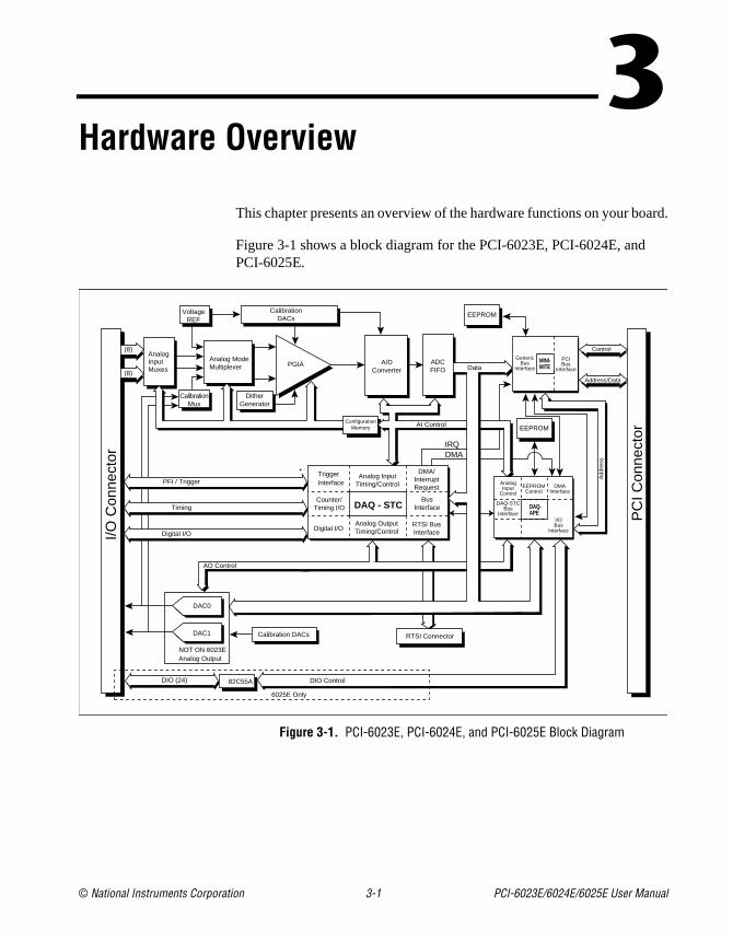
Figure 3-1 shows a block diagram for the PCI-6023E, PCI-6024E, andPCI-6025E.
Figure 3-1. PCI-6023E, PCI-6024E, and PCI-6025E Block Diagram
Timing
PFI / Trigger
DIO (24)
I/O C
onne
ctor
PC
I Con
nect
or
Digital I/O
A/DConverter
EEPROM
EEPROM
ConfigurationMemory
PGIA
CalibrationMux
Analog ModeMultiplexer
AnalogInputMuxes
VoltageREF
CalibrationDACs
Dither Generator
Calibration DACs
82C55A
DAC0
DAC1
NOT ON 6023EAnalog Output
DAQ - STC
Analog InputTiming/Control
Analog OutputTiming/ControlDigital I/O
TriggerInterface
Counter/Timing I/O
RTSI BusInterface
DMA/InterruptRequest
BusInterface
(8)
(8)
AI Control
Address/Data
Control
Data
AnalogInput
ControlEEPROMControl
DMAInterface
DAQ-APE
DAQ-STCBus
InterfaceI/OBus
Interface
MINI-MITE
GenericBus
Interface
PCIBus
Interface
IRQDMA
AO Control
ADCFIFO
Add
ress
RTSI Connector
DIO Control
6025E Only
25E User Manual
Chapter 3 Hardware Overview
ded
ls.
ions.
r to
put
g
PCI.book Page 2 Wednesday, September 16, 1998 9:09 AM
Analog InputThe analog input section of each board is software configurable. The following sections describe in detail each of the analog input settings.
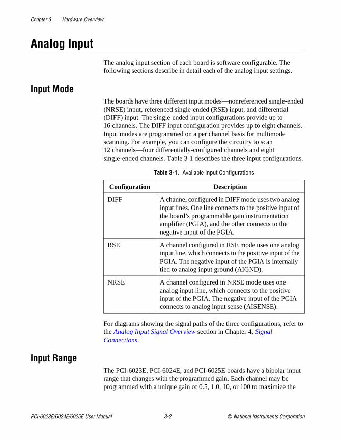
Input ModeThe boards have three different input modes—nonreferenced single-en(NRSE) input, referenced single-ended (RSE) input, and differential (DIFF) input. The single-ended input configurations provide up to 16 channels. The DIFF input configuration provides up to eight channeInput modes are programmed on a per channel basis for multimode scanning. For example, you can configure the circuitry to scan 12 channels—four differentially-configured channels and eight single-ended channels. Table 3-1 describes the three input configurat
For diagrams showing the signal paths of the three configurations, refethe Analog Input Signal Overview section in Chapter 4, Signal Connections.
Input RangeThe PCI-6023E, PCI-6024E, and PCI-6025E boards have a bipolar inrange that changes with the programmed gain. Each channel may be programmed with a unique gain of 0.5, 1.0, 10, or 100 to maximize the
Table 3-1. Available Input Configurations
Configuration Description
DIFF A channel configured in DIFF mode uses two analoginput lines. One line connects to the positive input ofthe board’s programmable gain instrumentation amplifier (PGIA), and the other connects to the negative input of the PGIA.
RSE A channel configured in RSE mode uses one analoinput line, which connects to the positive input of thePGIA. The negative input of the PGIA is internally tied to analog input ground (AIGND).
NRSE A channel configured in NRSE mode uses one analog input line, which connects to the positive input of the PGIA. The negative input of the PGIA connects to analog input sense (AISENSE).
PCI-6023E/6024E/6025E User Manual 3-2 © National Instruments Corporation

Chapter 3 Hardware Overview
in t gain
n is f oise
bout s of
tral are
-2a
50 ble.
and istic
a
PCI.book Page 3 Wednesday, September 16, 1998 9:09 AM
12-bit analog-to-digital converter (ADC) resolution. With the proper gasetting, you can use the full resolution of the ADC to measure the inpusignal. Table 3-2 shows the input range and precision according to the used.
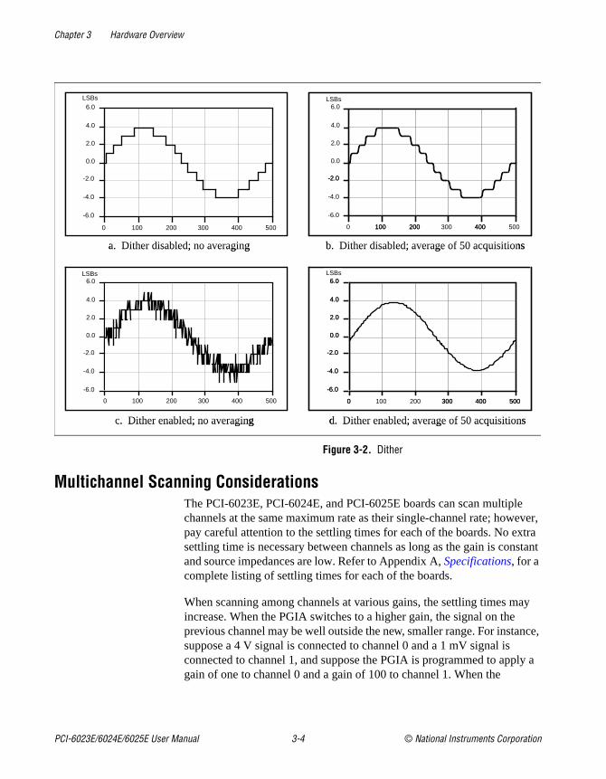
DitherWhen you enable dither, you add approximately 0.5 LSBrms of white Gaussian noise to the signal to be converted by the ADC. This additiouseful for applications involving averaging to increase the resolution oyour board, as in calibration or spectral analysis. In such applications, nmodulation is decreased and differential linearity is improved by the addition of the dither. When taking DC measurements, such as when checking the board calibration, you should enable dither and average a1,000 points to take a single reading. This process removes the effectquantization and reduces measurement noise, resulting in improved resolution. For high-speed applications not involving averaging or specanalysis, you may want to disable the dither to reduce noise. Your softwenables and disables the dither circuitry.
Figure 3-2 illustrates the effect of dither on signal acquisition. Figure 3shows a small (±4 LSB) sine wave acquired with dither off. The ADC quantization is clearly visible. Figure 3-2b shows what happens when such acquisitions are averaged together; quantization is still plainly visiIn Figure 3-2c, the sine wave is acquired with dither on. There is a considerable amount of visible noise, but averaging about 50 such acquisitions, as shown in Figure 3-2d, eliminates both the added noisethe effects of quantization. Dither has the effect of forcing quantizationnoise to become a zero-mean random variable rather than a determinfunction of the input signal.
Table 3-2. Measurement Precision
Gain Input Range Precision *
0.5
1.0
10.0
100.0
-10 to +10V
-5 to +5V
-500 to +500 mV
-50 to +50 mV
4.88 mV
2.44 mV
244.14 µV
24.41 µV
*The value of 1 LSB of the 12-bit ADC; that is, the voltage increment corresponding tochange of one count in the ADC 12-bit count.
Note: See Appendix A, Specifications, for absolute maximum ratings.
© National Instruments Corporation 3-3 PCI-6023E/6024E/6025E User Manual
Chapter 3 Hardware Overview
ever, tra stant
ay
nce,
ly a
PCI.book Page 4 Wednesday, September 16, 1998 9:09 AM
Figure 3-2. Dither
Multichannel Scanning ConsiderationsThe PCI-6023E, PCI-6024E, and PCI-6025E boards can scan multiplechannels at the same maximum rate as their single-channel rate; howpay careful attention to the settling times for each of the boards. No exsettling time is necessary between channels as long as the gain is conand source impedances are low. Refer to Appendix A, Specifications, for a complete listing of settling times for each of the boards.
When scanning among channels at various gains, the settling times mincrease. When the PGIA switches to a higher gain, the signal on the previous channel may be well outside the new, smaller range. For instasuppose a 4 V signal is connected to channel 0 and a 1 mV signal is connected to channel 1, and suppose the PGIA is programmed to appgain of one to channel 0 and a gain of 100 to channel 1. When the
a. Dither disabled; no averaging b. Dither disabled; average of 50 acquisitions
c. Dither enabled; no averaging
100 200 300 4000 500
-4.0
-2.0
0.0
2.0
4.0
-6.0
d. Dither enabled; average of 50 acquisitions
LSBs
LSBsLSBs
LSBs
6.0
100 200 300 4000 500
-4.0
-2.0
0.0
2.0
4.0
-6.0
6.0
100 200 300 4000 500
-4.0
-2.0
0.0
2.0
4.0
-6.0
6.0
100 200 300 4000 500
-4.0
-2.0
0.0
2.0
4.0
-6.0
6.0
PCI-6023E/6024E/6025E User Manual 3-4 © National Instruments Corporation
Chapter 3 Hardware Overview
00,
to not
ls
hen gh, ime under
m ss nals and l
ts
nt
th as
PCI.book Page 5 Wednesday, September 16, 1998 9:09 AM
multiplexer switches to channel 1 and the PGIA switches to a gain of 1the new full-scale range is ±50 mV.
The approximately 4 V step from 4 V to 1 mV is 4,000% of the new full-scale range. It may take as long as 100 µs for the circuitry to settle1 LSB after such a large transition. In general, this extra settling time isneeded when the PGIA is switching to a lower gain.
Settling times can also increase when scanning high-impedance signadue to a phenomenon called charge injection, where the analog input multiplexer injects a small amount of charge into each signal source wthat source is selected. If the impedance of the source is not low enouthe effect of the charge—a voltage error—will not have decayed by the tthe ADC samples the signal. For this reason, keep source impedances 1 kΩ to perform high-speed scanning.
Due to the previously described limitations of settling times resulting frothese conditions, multiple-channel scanning is not recommended unlesampling rates are low enough or it is necessary to sample several sigas nearly simultaneously as possible. The data is much more accuratechannel-to-channel independent if you acquire data from each channeindependently (for example, 100 points from channel 0, then 100 poinfrom channel 1, then 100 points from channel 2, and so on.)
Analog Output
♦ (PCI-6025E and PCI-6024E Only)
These boards supply two channels of analog output voltage at the I/Oconnector. The bipolar range is fixed at ±10 V. Data written to the digital-to-analog converter (DAC) will be interpreted as two’s complemeformat.
Analog Output GlitchIn normal operation, a DAC output will glitch whenever it is updated wia new value. The glitch energy differs from code to code and appearsdistortion in the frequency spectrum.
© National Instruments Corporation 3-5 PCI-6023E/6024E/6025E User Manual

Chapter 3 Hardware Overview
of
p
re e
rface port. ed
ree as and fers.
bus d to
be
e of
PCI.book Page 6 Wednesday, September 16, 1998 9:09 AM
Digital I/OThe PCI-6023E, PCI-6024, and PCI-6025E boards contain eight linesdigital I/O (DIO<0..7>) for general-purpose use. You can individually software-configure each line for either input or output. At system startuand reset, the digital I/O ports are all high impedance.
The hardware up/down control for general-purpose counters 0 and 1 aconnected onboard to DIO6 and DIO7, respectively. Thus, you can usDIO6 and DIO7 to control the general-purpose counters. The up/downcontrol signals are input only and do not affect the operation of the DIOlines.
♦ PCI-6025E only:
The PCI-6025E board uses an 82C55A Programmable Peripheral Inteto provide an additional 24 lines of digital I/O that represent three 8-bitports: PA, PB, PC. Each port can be programmed as an input or output The 82C55A has three modes of operation: simple I/O (mode 0), strobI/O (mode 1), and bidirectional I/O (mode 2). In modes 1 and 2, the thports are divided into two groups: group A and group B. Each group height data bits, plus control and status bits from Port C (PC). Modes 1 2 use handshaking signals from the computer to synchronize data transRefer to Chapter 4, Signal Connections, for more detailed information.
Timing Signal RoutingThe DAQ-STC chip provides a flexible interface for connecting timing signals to other boards or external circuitry. Your board uses the RTSIto interconnect timing signals between boards, and the ProgrammableFunction Input (PFI) pins on the I/O connector to connect the board toexternal circuitry. These connections are designed to enable the boarboth control and be controlled by other boards and circuits.
There are a total of 13 timing signals internal to the DAQ-STC that cancontrolled by an external source. These timing signals can also be controlled by signals generated internally to the DAQ-STC, and these selections are fully software-configurable. Figure 3-3 shows an examplthe signal routing multiplexer controlling the CONVERT* signal.
PCI-6023E/6024E/6025E User Manual 3-6 © National Instruments Corporation
Chapter 3 Hardware Overview
f the
ins,
are ing urce an g
eme r for I e
PCI.book Page 7 Wednesday, September 16, 1998 9:09 AM
Figure 3-3. CONVERT* Signal Routing
This figure shows that CONVERT* can be generated from a number osources, including the external signals RTSI<0..6> and PFI<0..9> andinternal signals Sample Interval Counter TC and GPCTR0_OUT.
Many of these timing signals are also available as outputs on the RTSI pas indicated in the RTSI Triggers section in this chapter, and on the PFI pins, as indicated in Chapter 4, Signal Connections.
Programmable Function InputsTen PFI pins are available on the board connector as PFI<0..9> and connected to the board’s internal signal routing multiplexer for each timsignal. Software can select any one of the PFI pins as the external sofor a given timing signal. It is important to note that any of the PFI pins cbe used as an input by any of the timing signals and that multiple timinsignals can use the same PFI simultaneously. This flexible routing schreduces the need to change physical connections to the I/O connectodifferent applications. You can also individually enable each of the PFpins to output a specific internal timing signal. For example, if you need th
RTSI Trigger <0..6>
PFI<0..9>
CONVERT*
Sample Interval Counter TC
GPCTR0_OUT
© National Instruments Corporation 3-7 PCI-6023E/6024E/6025E User Manual

Chapter 3 Hardware Overview
on
, or
se se nal
ceive us,
fault he
bus.
PCI.book Page 8 Wednesday, September 16, 1998 9:09 AM
UPDATE* signal as an output on the I/O connector, software can turnthe output driver for the PFI5/UPDATE* pin.
Board and RTSI ClocksMany board functions require a frequency timebase to generate the necessary timing signals for controlling A/D conversions, DAC updatesgeneral-purpose signals at the I/O connector.
These boards can use either its internal 20 MHz timebase or a timebareceived over the RTSI bus. In addition, if you configure the board to uthe internal timebase, you can also program the board to drive its intertimebase over the RTSI bus to another board that is programmed to rethis timebase signal. This clock source, whether local or from the RTSI bis used directly by the board as the primary frequency source. The deconfiguration at startup is to use the internal timebase without driving tRTSI bus timebase signal. This timebase is software selectable.
RTSI TriggersThe seven RTSI trigger lines on the RTSI bus provide a very flexible interconnection scheme for any PCI E Series board sharing the RTSI These bidirectional lines can drive any of eight timing signals onto theRTSI bus and can receive any of these timing signals. This signal connection scheme is shown in Figure 3-4.
PCI-6023E/6024E/6025E User Manual 3-8 © National Instruments Corporation
Chapter 3 Hardware Overview
PCI.book Page 9 Wednesday, September 16, 1998 9:09 AM
Figure 3-4. RTSI Bus Signal Connection
Refer to the Timing Connections section of Chapter 4, Signal Connections, for a description of the signals shown in Figure 3-4.
RT
SI B
us C
onne
ctor
switch
RT
SI S
witc
h
Clock
Trigger
7
DAQ-STC
TRIG1
TRIG2
CONVERT*
UPDATE*
WFTRIG
GPCTR0_SOURCE
GPCTR0_GATE
GPCTR0_OUT
STARTSCAN
AIGATE
SISOURCE
UISOURCE
GPCTR1_SOURCE
GPCTR1_GATE
RTSI_OSC (20 MHz)
© National Instruments Corporation 3-9 PCI-6023E/6024E/6025E User Manual
© National Instruments Corporation 4-1 PCI-6023E/6024E/60
PCI.book Page 1 Wednesday, September 16, 1998 9:09 AM
4
s toou the
ct nect or to
the he
s s
.
Signal Connections
This chapter describes how to make input and output signal connectionyour board via the I/O connector.
The I/O connector for the PCI-6023 and PCI-6024E has 68 pins that ycan connect to 68-pin accessories with the SH6868 shielded cable or R6868 ribbon cable. You can connect your board to 50-pin signal accessories with the SH6850 shielded cable or R6850 ribbon cable.
The I/O connector for the PCI-6025E has 100 pins that you can conneto 100-pin accessories with the SH100100 shielded cable. You can conyour board to 68-pin accessories with the SH1006868 shielded cable, 50-pin accessories with the R1005050 ribbon cable.
I/O ConnectorFigure 4-1 shows the pin assignments for the 68-pin I/O connector onPCI-6023 and PCI-6024E. Figure 4-2 shows the pin assignments for t100-pin I/O connector on the PCI-6025E. Refer to Appendix B, Custom Cabling and Optional Connectors, for pin assignments of the optional 50- and 68-pin connectors. A signal description follows the figures.
Caution Connections that exceed any of the maximum ratings of input or output signalon the boards can damage the board and the computer. Maximum input ratingfor each signal are given in the Protection column of Table 4-2. National Instruments is NOT liable for any damages resulting from such signal connections
!
25E User Manual

Chapter 4 Signal Connections
PCI.book Page 2 Wednesday, September 16, 1998 9:09 AM
Figure 4-1. I/O Connector Pin Assignment for the PCI-6023E/PCI-6024E
FREQ_OUT
GPCTR0_OUT
PFI9/GPCTR0_GATE
DGND
PFI6/WFTRIG
PFI5/UPDATE*
DGND
+5 VDGND
PFI1/TRIG2
PFI0/TRIG1
DGND
DGND
+5 V
DGNDDIO6
DIO1
DGND
DIO4
RESERVED DAC1OUT1
DAC0OUT1
ACH15AIGND
ACH6ACH13
AIGND
ACH4
AIGNDACH3
ACH10
AIGND
ACH1ACH8
DGND
1 Not available on the PCI-6023E
PFI8/GPCTR0_SOURCE
PFI7/STARTSCAN
GPCTR1_OUT
PFI4/GPCTR1_GATE
PFI3/GPCTR1_SOURCE
PFI2/CONVERT*
DGND
DGND
DGND
EXTSTROBE*
SCANCLK
DIO3
DIO7
DIO2DGND
DIO5
DIO0
DGND
AOGND
AOGND
AIGND
ACH7
ACH14
AIGND
ACH5
ACH12
AISENSE
ACH11
AIGND
ACH2
ACH9
AIGNDACH0
1 35
2 36
3 37
4 38
5 39
6 40
7 41
8 42
9 43
10 44
11 45
12 46
13 47
14 48
15 49
16 50
17 51
18 52
19 53
20 54
21 55
22 56
23 57
24 58
25 59
26 60
27 61
28 62
29 63
30 64
31 65
32 66
33 67
34 68
PCI-6023E/6024E/6025E User Manual 4-2 © National Instruments Corporation

Chapter 4 Signal Connections
PCI.book Page 3 Wednesday, September 16, 1998 9:09 AM
Figure 4-2. I/O Connector Pin Assignment for the PCI-6025E
50 10049 9948 9847 9746 9645 9544 9443 9342 9241 9140 9039 89
38 8837 8736 8635 8534 8433 8332 8231 8130 8029 7928 7827 7726 7625 7524 7423 7322 7221 7120 7019 6918 6817 6716 6615 6514 6413 6312 6211 6110 609 598 587 576 565 554 543 532 521 51
FREQ_OUT GNDGPCTR0_OUT +5 V
PFI9/GPCTR0_GATE GNDPFI8/GPCTR0_SOURCE PA0
PFI7/STARTSCAN GNDPFI6/WFTRIG PA1
PFI5/UPDATE* GNDGPCTR1_OUT PA2
PFI4/GPCTR1_GATE GNDPFI3/GPCTR1_SOURCE PA3
PFI2/CONVERT* GNDPFI1/TRIG2 PA4
PFI0/TRIG1 GNDEXTSTROBE* PA5
SCANCLK GND+5 V PA6+5 V GND
DGND PA7DIO7 GNDDIO3 PB0DIO6 GNDDIO2 PB1DIO5 GNDDIO1 PB2DIO4 GNDDIO0 PB3
DGND GNDAOGND PB4
RESERVED GNDDAC1OUT PB5DAC0OUT GNDAISENSE PB6
ACH15 GNDACH7 PB7
ACH14 GNDACH6 PC0
ACH13 GNDACH5 PC1
ACH12 GNDACH4 PC2
ACH11 GNDACH3 PC3
ACH10 GNDACH2 PC4ACH9 GNDACH1 PC5ACH8 GNDACH0 PC6
AIGND GNDAIGND PC7
© National Instruments Corporation 4-3 PCI-6023E/6024E/6025E User Manual
Chapter 4 Signal Connections
3E,
e
PCI.book Page 4 Wednesday, September 16, 1998 9:09 AM
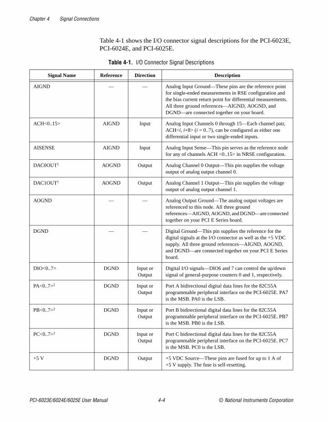
Table 4-1 shows the I/O connector signal descriptions for the PCI-602PCI-6024E, and PCI-6025E.
Table 4-1. I/O Connector Signal Descriptions
Signal Name Reference Direction Description
AIGND — — Analog Input Ground—These pins are the reference point for single-ended measurements in RSE configuration and the bias current return point for differential measurements.All three ground references—AIGND, AOGND, and DGND—are connected together on your board.
ACH<0..15> AIGND Input Analog Input Channels 0 through 15—Each channel pair, ACH<i, i+8> (i = 0..7), can be configured as either one differential input or two single-ended inputs.
AISENSE AIGND Input Analog Input Sense—This pin serves as the reference nodfor any of channels ACH <0..15> in NRSE configuration.
DAC0OUT1 AOGND Output Analog Channel 0 Output—This pin supplies the voltage output of analog output channel 0.
DAC1OUT1 AOGND Output Analog Channel 1 Output—This pin supplies the voltage output of analog output channel 1.
AOGND — — Analog Output Ground—The analog output voltages are referenced to this node. All three ground references—AIGND, AOGND, and DGND—are connected together on your PCI E Series board.
DGND — — Digital Ground—This pin supplies the reference for the digital signals at the I/O connector as well as the +5 VDC supply. All three ground references—AIGND, AOGND, and DGND—are connected together on your PCI E Seriesboard.
DIO<0..7> DGND Input or Output
Digital I/O signals—DIO6 and 7 can control the up/down signal of general-purpose counters 0 and 1, respectively.
PA<0..7>2 DGND Input or Output
Port A bidirectional digital data lines for the 82C55A programmable peripheral interface on the PCI-6025E. PA7is the MSB. PA0 is the LSB.
PB<0..7>2 DGND Input or Output
Port B bidirectional digital data lines for the 82C55A programmable peripheral interface on the PCI-6025E. PB7is the MSB. PB0 is the LSB.
PC<0..7>2 DGND Input or Output
Port C bidirectional digital data lines for the 82C55A programmable peripheral interface on the PCI-6025E. PC7is the MSB. PC0 is the LSB.
+5 V DGND Output +5 VDC Source—These pins are fused for up to 1 A of +5 V supply. The fuse is self-resetting.
PCI-6023E/6024E/6025E User Manual 4-4 © National Instruments Corporation
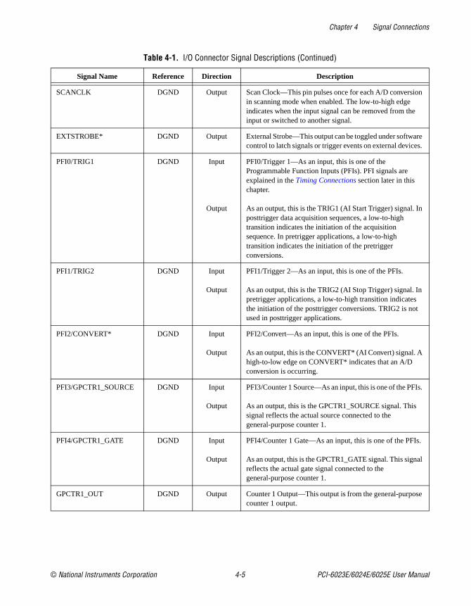
Chapter 4 Signal Connections
.
.
PCI.book Page 5 Wednesday, September 16, 1998 9:09 AM
SCANCLK DGND Output Scan Clock—This pin pulses once for each A/D conversionin scanning mode when enabled. The low-to-high edge indicates when the input signal can be removed from the input or switched to another signal.
EXTSTROBE* DGND Output External Strobe—This output can be toggled under softwarecontrol to latch signals or trigger events on external devices
PFI0/TRIG1 DGND Input
Output
PFI0/Trigger 1—As an input, this is one of the Programmable Function Inputs (PFIs). PFI signals are explained in the Timing Connections section later in this chapter.
As an output, this is the TRIG1 (AI Start Trigger) signal. In posttrigger data acquisition sequences, a low-to-high transition indicates the initiation of the acquisition sequence. In pretrigger applications, a low-to-high transition indicates the initiation of the pretrigger conversions.
PFI1/TRIG2 DGND Input
Output
PFI1/Trigger 2—As an input, this is one of the PFIs.
As an output, this is the TRIG2 (AI Stop Trigger) signal. In pretrigger applications, a low-to-high transition indicates the initiation of the posttrigger conversions. TRIG2 is not used in posttrigger applications.
PFI2/CONVERT* DGND Input
Output
PFI2/Convert—As an input, this is one of the PFIs.
As an output, this is the CONVERT* (AI Convert) signal. A high-to-low edge on CONVERT* indicates that an A/D conversion is occurring.
PFI3/GPCTR1_SOURCE DGND Input
Output
PFI3/Counter 1 Source—As an input, this is one of the PFIs
As an output, this is the GPCTR1_SOURCE signal. This signal reflects the actual source connected to the general-purpose counter 1.
PFI4/GPCTR1_GATE DGND Input
Output
PFI4/Counter 1 Gate—As an input, this is one of the PFIs.
As an output, this is the GPCTR1_GATE signal. This signalreflects the actual gate signal connected to the general-purpose counter 1.
GPCTR1_OUT DGND Output Counter 1 Output—This output is from the general-purposecounter 1 output.
Table 4-1. I/O Connector Signal Descriptions (Continued)
Signal Name Reference Direction Description
© National Instruments Corporation 4-5 PCI-6023E/6024E/6025E User Manual
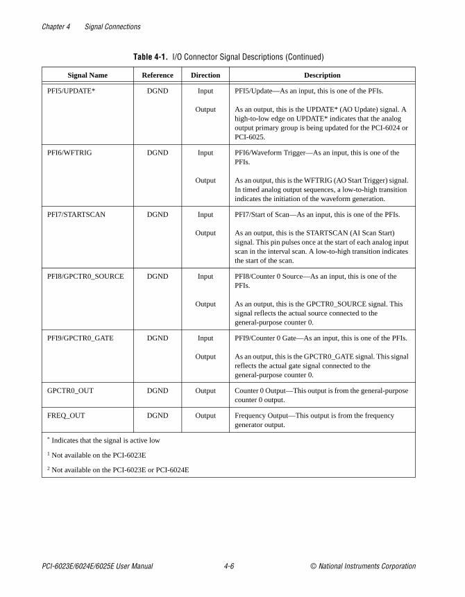
Chapter 4 Signal Connections
t
PCI.book Page 6 Wednesday, September 16, 1998 9:09 AM
PFI5/UPDATE* DGND Input
Output
PFI5/Update—As an input, this is one of the PFIs.
As an output, this is the UPDATE* (AO Update) signal. A high-to-low edge on UPDATE* indicates that the analog output primary group is being updated for the PCI-6024 orPCI-6025.
PFI6/WFTRIG DGND Input
Output
PFI6/Waveform Trigger—As an input, this is one of the PFIs.
As an output, this is the WFTRIG (AO Start Trigger) signal. In timed analog output sequences, a low-to-high transitionindicates the initiation of the waveform generation.
PFI7/STARTSCAN DGND Input
Output
PFI7/Start of Scan—As an input, this is one of the PFIs.
As an output, this is the STARTSCAN (AI Scan Start) signal. This pin pulses once at the start of each analog inpuscan in the interval scan. A low-to-high transition indicates the start of the scan.
PFI8/GPCTR0_SOURCE DGND Input
Output
PFI8/Counter 0 Source—As an input, this is one of the PFIs.
As an output, this is the GPCTR0_SOURCE signal. This signal reflects the actual source connected to the general-purpose counter 0.
PFI9/GPCTR0_GATE DGND Input
Output
PFI9/Counter 0 Gate—As an input, this is one of the PFIs.
As an output, this is the GPCTR0_GATE signal. This signalreflects the actual gate signal connected to the general-purpose counter 0.
GPCTR0_OUT DGND Output Counter 0 Output—This output is from the general-purposecounter 0 output.
FREQ_OUT DGND Output Frequency Output—This output is from the frequency generator output.
* Indicates that the signal is active low
1 Not available on the PCI-6023E
2 Not available on the PCI-6023E or PCI-6024E
Table 4-1. I/O Connector Signal Descriptions (Continued)
Signal Name Reference Direction Description
PCI-6023E/6024E/6025E User Manual 4-6 © National Instruments Corporation
Chapter 4 Signal Connections
E,
PCI.book Page 7 Wednesday, September 16, 1998 9:09 AM
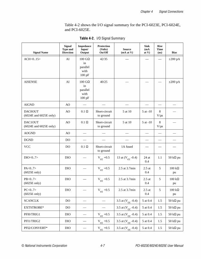
Table 4-2 shows the I/O signal summary for the PCI-6023E, PCI-6024and PCI-6025E.
Table 4-2. I/O Signal Summary
Signal Name
Signal Type and Direction
Impedance Input/Output
Protection (Volts) On/Off
Source (mA at V)
Sink (mA at V)
Rise Time (ns) Bias
ACH<0..15> AI 100 GΩ in
parallel with
100 pF
42/35 — — — ±200 pA
AISENSE AI 100 GΩ in
parallel with
100 pF
40/25 — — — ±200 pA
AIGND AO — — — — — —
DAC0OUT(6024E and 6025E only)
AO 0.1Ω Short-circuit to ground
5 at 10 5 at -10 8 V/µs
—
DAC1OUT (6024E and 6025E only)
AO 0.1Ω Short-circuit to ground
5 at 10 5 at -10 8 V/µs
—
AOGND AO — — — — — —
DGND DO — — — — — —
VCC DO 0.1Ω Short-circuit to ground
1A fused — — —
DIO<0..7> DIO — Vcc +0.5 13 at (Vcc -0.4) 24 at 0.4
1.1 50 kΩ pu
PA<0..7>(6025E only)
DIO — Vcc +0.5 2.5 at 3.7min 2.5 at 0.4
5 100 kΩ pu
PB<0..7>(6025E only)
DIO — Vcc +0.5 2.5 at 3.7min 2.5 at 0.4
5 100 kΩ pu
PC<0..7>(6025E only)
DIO — Vcc +0.5 2.5 at 3.7min 2.5 at 0.4
5 100 kΩ pu
SCANCLK DO — — 3.5 at (Vcc -0.4) 5 at 0.4 1.5 50 kΩ pu
EXTSTROBE* DO — — 3.5 at (Vcc -0.4) 5 at 0.4 1.5 50 kΩ pu
PFI0/TRIG1 DIO — Vcc +0.5 3.5 at (Vcc -0.4) 5 at 0.4 1.5 50 kΩ pu
PFI1/TRIG2 DIO — Vcc +0.5 3.5 at (Vcc -0.4) 5 at 0.4 1.5 50 kΩ pu
PFI2/CONVERT* DIO — Vcc +0.5 3.5 at (Vcc -0.4) 5 at 0.4 1.5 50 kΩ pu
© National Instruments Corporation 4-7 PCI-6023E/6024E/6025E User Manual

Chapter 4 Signal Connections
and ds put
rent
PCI.book Page 8 Wednesday, September 16, 1998 9:09 AM
Analog Input Signal Overview
The analog input signals for these boards are ACH<0..15>, ASENSE, AIGND. Connection of these analog input signals to your board depenon the type of input signal source and the configuration of the analog inchannels you are using. This section provides an overview of the diffetypes of signal sources and analog input configuration modes. More specific signal connection information is provided in the section, Analog Input Signal Connections.
Types of Signal SourcesWhen configuring the input channels and making signal connections, you must first determine whether the signal sources are floating or ground-referenced.
PFI3/GPCTR1_SOURCE DIO — Vcc +0.5 3.5 at (Vcc -0.4) 5 at 0.4 1.5 50 kΩ pu
PFI4/GPCTR1_GATE DIO — Vcc +0.5 3.5 at (Vcc -0.4) 5 at 0.4 1.5 50 kΩ pu
GPCTR1_OUT DO — — 3.5 at (Vcc -0.4) 5 at 0.4 1.5 50 kΩ pu
PFI5/UPDATE* DIO — Vcc +0.5 3.5 at (Vcc -0.4) 5 at 0.4 1.5 50 kΩ pu
PFI6/WFTRIG DIO — Vcc +0.5 3.5 at (Vcc -0.4) 5 at 0.4 1.5 50 kΩ pu
PFI7/STARTSCAN DIO — Vcc +0.5 3.5 at (Vcc -0.4) 5 at 0.4 1.5 50 kΩ pu
PFI8/GPCTR0_SOURCE DIO — Vcc +0.5 3.5 at (Vcc -0.4) 5 at 0.4 1.5 50 kΩ pu
PFI9/GPCTR0_GATE DIO — Vcc +0.5 3.5 at (Vcc -0.4) 5 at 0.4 1.5 50 kΩ pu
GPCTR0_OUT DO — — 3.5 at (Vcc -0.4) 5 at 0.4 1.5 50 kΩ pu
FREQ_OUT DO — — 3.5 at (Vcc-0.4) 5 at 0.4 1.5 50 kΩ pu
AI = Analog Input DIO = Digital Input/Output pu = pullupAO = Analog Output DO = Digital Output
Note: The tolerance on the 50 kΩ pullup and pulldown resistors is very large. Actual value may range between 17 kΩ and 100 kΩ.
Table 4-2. I/O Signal Summary (Continued)
Signal Name
Signal Type and Direction
Impedance Input/Output
Protection (Volts) On/Off
Source (mA at V)
Sink (mA at V)
Rise Time (ns) Bias
PCI-6023E/6024E/6025E User Manual 4-8 © National Instruments Corporation

Chapter 4 Signal Connections
nd ples
rce.
nal. f the
on nts ory.
to can d. y r
ial
ced
PCI.book Page 9 Wednesday, September 16, 1998 9:09 AM
Floating Signal SourcesA floating signal source is not connected in any way to the building grousystem but, rather, has an isolated ground-reference point. Some examof floating signal sources are outputs of transformers, thermocouples,battery-powered devices, optical isolators, and isolation amplifiers. Aninstrument or device that has an isolated output is a floating signal souYou must tie the ground reference of a floating signal to your board’s analog input ground to establish a local or onboard reference for the sigOtherwise, the measured input signal varies as the source floats out ocommon-mode input range.
Ground-Referenced Signal SourcesA ground-referenced signal source is connected in some way to the building system ground and is, therefore, already connected to a commground point with respect to the board, assuming that the computer isplugged into the same power system. Nonisolated outputs of instrumeand devices that plug into the building power system fall into this categ
The difference in ground potential between two instruments connectedthe same building power system is typically between 1 and 100 mV butbe much higher if power distribution circuits are not properly connecteIf a grounded signal source is improperly measured, this difference maappear as an error in the measurement. The connection instructions fogrounded signal sources are designed to eliminate this ground potentdifference from the measured signal.
Analog Input ModesYou can configure your board for one of three input modes: nonreferensingle ended (NRSE), referenced single ended (RSE), and differential(DIFF). With the different configurations, you can use the PGIA in different ways. Figure 4-3 shows a diagram of your board’s PGIA.
© National Instruments Corporation 4-9 PCI-6023E/6024E/6025E User Manual
Chapter 4 Signal Connections
15> ls nd e
nd
tive IFF
alog
nts ard. ugh o a the
PCI.book Page 10 Wednesday, September 16, 1998 9:09 AM
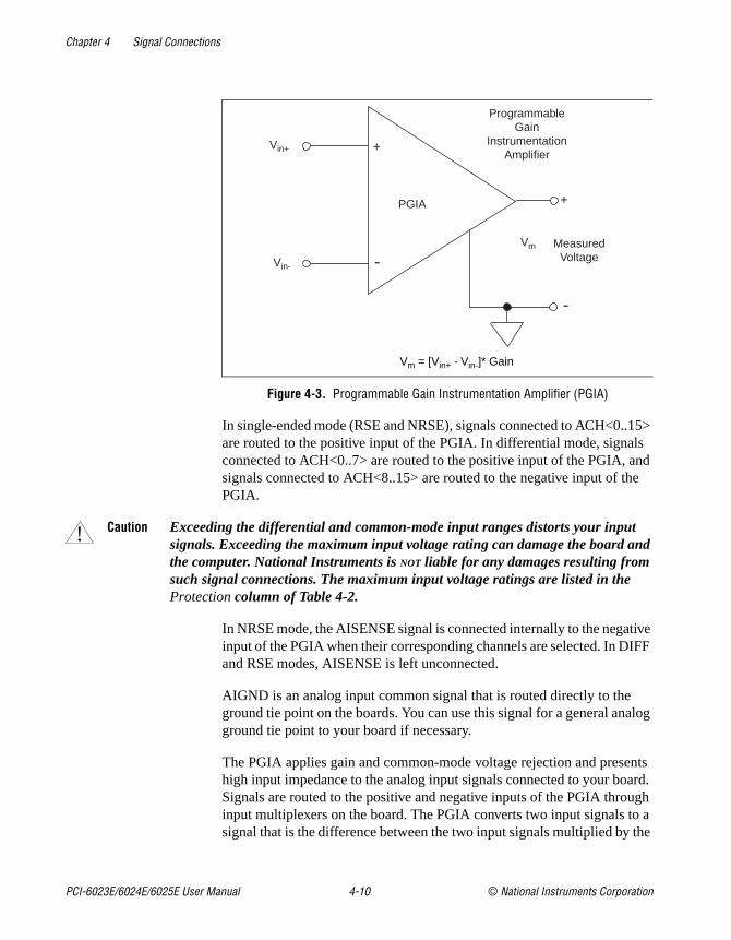
Figure 4-3. Programmable Gain Instrumentation Amplifier (PGIA)
In single-ended mode (RSE and NRSE), signals connected to ACH<0..are routed to the positive input of the PGIA. In differential mode, signaconnected to ACH<0..7> are routed to the positive input of the PGIA, asignals connected to ACH<8..15> are routed to the negative input of thPGIA.
Caution Exceeding the differential and common-mode input ranges distorts your input signals. Exceeding the maximum input voltage rating can damage the board athe computer. National Instruments is NOT liable for any damages resulting from such signal connections. The maximum input voltage ratings are listed in the Protection column of Table 4-2.
In NRSE mode, the AISENSE signal is connected internally to the negainput of the PGIA when their corresponding channels are selected. In Dand RSE modes, AISENSE is left unconnected.
AIGND is an analog input common signal that is routed directly to the ground tie point on the boards. You can use this signal for a general anground tie point to your board if necessary.
The PGIA applies gain and common-mode voltage rejection and presehigh input impedance to the analog input signals connected to your boSignals are routed to the positive and negative inputs of the PGIA throinput multiplexers on the board. The PGIA converts two input signals tsignal that is the difference between the two input signals multiplied by
-
Programmable Gain
InstrumentationAmplifier
-
MeasuredVoltage
Vm
+
+
PGIA
Vin+
Vin-
Vm = [Vin+ - Vin-]* Gain
!
PCI-6023E/6024E/6025E User Manual 4-10 © National Instruments Corporation

Chapter 4 Signal Connections
to this
at al
n this
l
PCI.book Page 11 Wednesday, September 16, 1998 9:09 AM
gain setting of the amplifier. The amplifier output voltage is referencedthe ground for the board. Your board’s A/D converter (ADC) measures output voltage when it performs A/D conversions.
You must reference all signals to ground either at the source device orthe board. If you have a floating source, you should reference the signto ground by using the RSE input mode or the DIFF input configuratiowith bias resistors (see the Differential Connections for Nonreferenced orFloating Signal Sources section in this chapter). If you have a groundedsource, you should not reference the signal to AIGND. You can avoid reference by using DIFF or NRSE input configurations.
Analog Input Signal ConnectionsThe following sections discuss the use of single-ended and differentiameasurements and recommendations for measuring both floating andground-referenced signal sources.
Figure 4-4 summarizes the recommended input configuration for bothtypes of signal sources.
© National Instruments Corporation 4-11 PCI-6023E/6024E/6025E User Manual
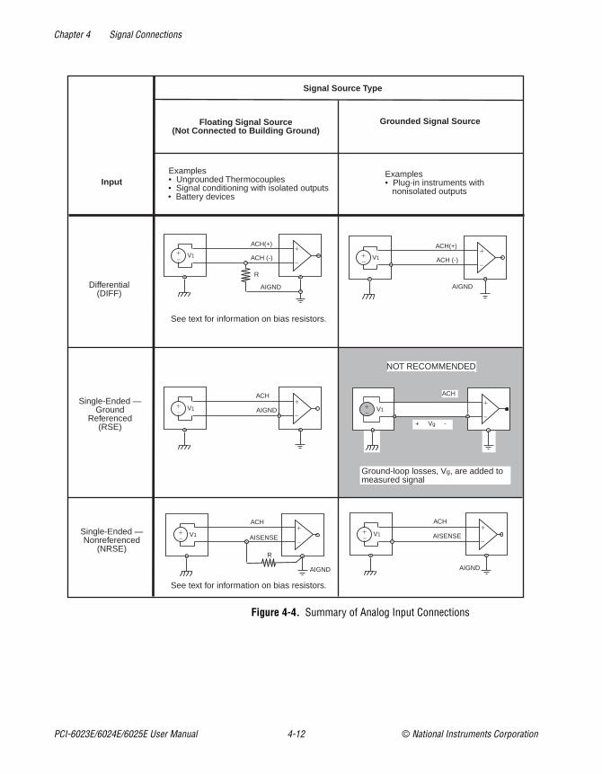
Chapter 4 Signal Connections
PCI.book Page 12 Wednesday, September 16, 1998 9:09 AM
Figure 4-4. Summary of Analog Input Connections
Input
Differential(DIFF)
Single-Ended —Ground
Referenced(RSE)
Single-Ended —Nonreferenced
(NRSE)
Floating Signal Source(Not Connected to Building Ground)
Grounded Signal Source
Examples• Ungrounded Thermocouples• Signal conditioning with isolated outputs• Battery devices
Examples• Plug-in instruments with nonisolated outputs
+
-+-
V1
ACH(+)+
-+-
V1
ACH(+)
ACH (-)
See text for information on bias resistors.
See text for information on bias resistors.
R
Signal Source Type
ACH (-)
AIGND
+
-+-
V1
ACH
AIGND+
-
+-
NOT RECOMMENDED
ACH
+ Vg -
V1
Ground-loop losses, Vg, are added tomeasured signal
+
-+-
V1
ACH
AISENSE
R
AIGND
+
-+-
V1
ACH
AISENSE
AIGND
AIGND
PCI-6023E/6024E/6025E User Manual 4-12 © National Instruments Corporation

Chapter 4 Signal Connections
wn e t
, or
wo ht
ts
urn
w
PCI.book Page 13 Wednesday, September 16, 1998 9:09 AM
Differential Connection Considerations (DIFF Input Configuration)A differential connection is one in which the analog input signal has its oreference signal or signal return path. These connections are availablwhen the selected channel is configured in DIFF input mode. The inpusignal is tied to the positive input of the PGIA, and its reference signalreturn, is tied to the negative input of the PGIA.
When you configure a channel for differential input, each signal uses tmultiplexer inputs—one for the signal and one for its reference signal.Therefore, with a differential configuration for every channel, up to eiganalog input channels are available.
You should use differential input connections for any channel that meeany of the following conditions:
• The input signal is low level (less than 1 V).
• The leads connecting the signal to the board are greater than10 ft (3 m).
• The input signal requires a separate ground-reference point or retsignal.
• The signal leads travel through noisy environments.
Differential signal connections reduce picked up noise and increase common-mode noise rejection. Differential signal connections also alloinput signals to float within the common-mode limits of the PGIA.
© National Instruments Corporation 4-13 PCI-6023E/6024E/6025E User Manual
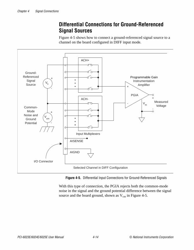
Chapter 4 Signal Connections
o a
nal
PCI.book Page 14 Wednesday, September 16, 1998 9:09 AM
Differential Connections for Ground-Referenced Signal SourcesFigure 4-5 shows how to connect a ground-referenced signal source tchannel on the board configured in DIFF input mode.
Figure 4-5. Differential Input Connections for Ground-Referenced Signals
With this type of connection, the PGIA rejects both the common-modenoise in the signal and the ground potential difference between the sigsource and the board ground, shown as Vcm in Figure 4-5.
Ground-Referenced
SignalSource
Common-Mode
Noise and GroundPotential
Input Multiplexers
AISENSE
InstrumentationAmplifier
VmMeasured
Voltage
AIGND
-
+
-
+
Vs
Vcm
+
-
-
+
I/O Connector
ACH+
ACH-
Selected Channel in DIFF Configuration
PGIA
Programmable Gain
PCI-6023E/6024E/6025E User Manual 4-14 © National Instruments Corporation

Chapter 4 Signal Connections
l
al e
The put
PCI.book Page 15 Wednesday, September 16, 1998 9:09 AM
Differential Connections for Nonreferenced or Floating Signal SourcesFigure 4-6 shows how to connect a floating signal source to a channeconfigured in DIFF input mode.
Figure 4-6. Differential Input Connections for Nonreferenced Signals
Figure 4-6 shows two bias resistors connected in parallel with the signleads of a floating signal source. If you do not use the resistors and thsource is truly floating, the source is not likely to remain within the common-mode signal range of the PGIA. The PGIA will then saturate,causing erroneous readings. You must reference the source to AIGND.easiest way is to connect the positive side of the signal to the positive in
+
-
+
FloatingSignalSource
Input Multiplexers
InstrumentationAmplifier
VmMeasured
Voltage-
VS
-
+
I/O Connector
AIGND
BiasCurrentReturnPaths
Biasresistors (see text)
ACH-
ACH+
AISENSE
Selected Channel in DIFF Configuration
PGIA
Programmable Gain
© National Instruments Corporation 4-15 PCI-6023E/6024E/6025E User Manual

Chapter 4 Signal Connections
ell
ce
e IA
ive
al onto
an
the 4-6. ut
IA eds oad age
tive own
PCI.book Page 16 Wednesday, September 16, 1998 9:09 AM
of the PGIA and connect the negative side of the signal to AIGND as was to the negative input of the PGIA, without any resistors at all. This connection works well for DC-coupled sources with low source impedan(less than 100Ω).
However, for larger source impedances, this connection leaves the differential signal path significantly out of balance. Noise that couples electrostatically onto the positive line does not couple onto the negativline because it is connected to ground. Hence, this noise appears as adifferential-mode signal instead of a common-mode signal, and the PGdoes not reject it. In this case, instead of directly connecting the negatline to AIGND, connect it to AIGND through a resistor that is about 100 times the equivalent source impedance. The resistor puts the signpath nearly in balance, so that about the same amount of noise couplesboth connections, yielding better rejection of electrostatically coupled noise. Also, this configuration does not load down the source (other ththe very high input impedance of the PGIA).
You can fully balance the signal path by connecting another resistor ofsame value between the positive input and AIGND, as shown in FigureThis fully balanced configuration offers slightly better noise rejection bhas the disadvantage of loading the source down with the series combination (sum) of the two resistors. If, for example, the source impedance is 2 kΩ and each of the two resistors is 100 kΩ, the resistors load down the source with 200 kΩ and produce a –1% gain error.
Both inputs of the PGIA require a DC path to ground in order for the PGto work. If the source is AC coupled (capacitively coupled), the PGIA nea resistor between the positive input and AIGND. If the source has lowimpedance, choose a resistor that is large enough not to significantly lthe source but small enough not to produce significant input offset voltas a result of input bias current (typically 100 kΩ to 1 MΩ). In this case, you can tie the negative input directly to AIGND. If the source has highoutput impedance, you should balance the signal path as previously described using the same value resistor on both the positive and negainputs; you should be aware that there is some gain error from loading dthe source.
PCI-6023E/6024E/6025E User Manual 4-16 © National Instruments Corporation
Chapter 4 Signal Connections
al is input the
log
eets
m).
or
pes ion. the ; in d the
he
ng al
PCI.book Page 17 Wednesday, September 16, 1998 9:09 AM
Single-Ended Connection ConsiderationsA single-ended connection is one in which the board analog input signreferenced to a ground that can be shared with other input signals. The signal is tied to the positive input of the PGIA, and the ground is tied to negative input of the PGIA.
When every channel is configured for single-ended input, up to 16 anainput channels are available.
You can use single-ended input connections for any input signal that mthe following conditions:
• The input signal is high level (greater than 1 V).
• The leads connecting the signal to the board are less than 10 ft (3
• The input signal can share a common reference point with other signals.
DIFF input connections are recommended for greater signal integrity fany input signal that does not meet the preceding conditions.
Using your software, you can configure the channels for two different tyof single-ended connections—RSE configuration and NRSE configuratThe RSE configuration is used for floating signal sources; in this case,board provides the reference ground point for the external signal. TheNRSE input configuration is used for ground-referenced signal sourcesthis case, the external signal supplies its own reference ground point anboard should not supply one.
In single-ended configurations, more electrostatic and magnetic noisecouples into the signal connections than in differential configurations. Tcoupling is the result of differences in the signal path. Magnetic coupliis proportional to the area between the two signal conductors. Electriccoupling is a function of how much the electric field differs between thetwo conductors.
© National Instruments Corporation 4-17 PCI-6023E/6024E/6025E User Manual
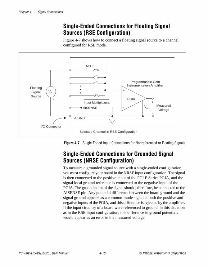
Chapter 4 Signal Connections
l
n, nal the the
the and ier. ion
PCI.book Page 18 Wednesday, September 16, 1998 9:09 AM
Single-Ended Connections for Floating Signal Sources (RSE Configuration)Figure 4-7 shows how to connect a floating signal source to a channeconfigured for RSE mode.
Figure 4-7. Single-Ended Input Connections for Nonreferenced or Floating Signals
Single-Ended Connections for Grounded Signal Sources (NRSE Configuration)To measure a grounded signal source with a single-ended configuratioyou must configure your board in the NRSE input configuration. The sigis then connected to the positive input of the PCI E Series PGIA, and signal local ground reference is connected to the negative input of thePGIA. The ground point of the signal should, therefore, be connected toAISENSE pin. Any potential difference between the board ground andsignal ground appears as a common-mode signal at both the positive negative inputs of the PGIA, and this difference is rejected by the amplifIf the input circuitry of a board were referenced to ground, in this situatas in the RSE input configuration, this difference in ground potentials would appear as an error in the measured voltage.
Vs
+
+
+
-
-
-
VmMeasured
Voltage
FloatingSignalSource
ACH
AIGND
I/O Connector
AISENSE
Selected Channel in RSE Configuration
PGIAInput Multiplexers
Programmable GainInstrumentation Amplifier
PCI-6023E/6024E/6025E User Manual 4-18 © National Instruments Corporation
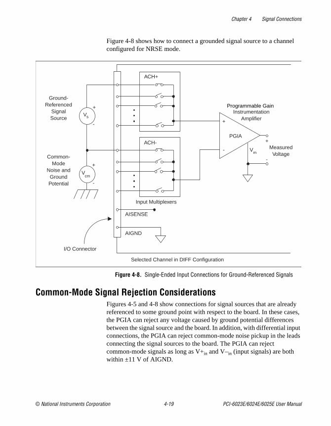
Chapter 4 Signal Connections
el
dy ses, s put ads
PCI.book Page 19 Wednesday, September 16, 1998 9:09 AM
Figure 4-8 shows how to connect a grounded signal source to a channconfigured for NRSE mode.
Figure 4-8. Single-Ended Input Connections for Ground-Referenced Signals
Common-Mode Signal Rejection ConsiderationsFigures 4-5 and 4-8 show connections for signal sources that are alreareferenced to some ground point with respect to the board. In these cathe PGIA can reject any voltage caused by ground potential differencebetween the signal source and the board. In addition, with differential inconnections, the PGIA can reject common-mode noise pickup in the leconnecting the signal sources to the board. The PGIA can reject common-mode signals as long as V+in and V–in (input signals) are both within ±11 V of AIGND.
Ground-Referenced
SignalSource
Common-Mode
Noise and GroundPotential
Input Multiplexers
AISENSE
InstrumentationAmplifier
VmMeasured
Voltage
AIGND
-
+
-
+
Vs
Vcm
+
-
-
+
I/O Connector
ACH+
ACH-
Selected Channel in DIFF Configuration
PGIA
Programmable Gain
© National Instruments Corporation 4-19 PCI-6023E/6024E/6025E User Manual

Chapter 4 Signal Connections
and
rd.
PCI.book Page 20 Wednesday, September 16, 1998 9:09 AM
Analog Output Signal Connections
♦ PCI-6024E and PCI-6025E
The analog output signals are DAC0OUT, DAC1OUT, and AOGND. DAC0OUT and DAC1OUT are not available on the PCI-6023E.
DAC0OUT is the voltage output signal for analog output channel 0. DAC1OUT is the voltage output signal for analog output channel 1.
AOGND is the ground reference signal for both analog output channelsthe external reference signal.
Figure 4-9 shows how to make analog output connections to your boa
Figure 4-9. Analog Output Connections
+
-
+
-
Channel 0
Channel 1
Load
Load
VOUT 0
VOUT 1DAC1OUT
AOGND
DAC0OUT
Analog Output Channels
I/O Connector
PCI-6023E/6024E/6025E User Manual 4-20 © National Instruments Corporation

Chapter 4 Signal Connections
re e ts
> e
PCI.book Page 21 Wednesday, September 16, 1998 9:09 AM
Digital I/O Signal Connections
All BoardsAll boards have digital I/O signals DIO<0..7> and DGND. DIO<0..7> athe signals making up the DIO port, and DGND is the ground referencsignal for the DIO port. You can program all lines individually to be inpuor outputs.
Figure 4-10 shows signal connections for three typical digital I/O applications.
Figure 4-10. Digital I/O Connections
Figure 4-10 shows DIO<0..3> configured for digital input and DIO<4..7configured for digital output. Digital input applications include receivingTTL signals and sensing external device states such as the state of th
LED
+5 V
TTL Signal
+5 V
DIO<4..7>
DIO<0..3>
DGND
Switch
I/O Connector
© National Instruments Corporation 4-21 PCI-6023E/6024E/6025E User Manual

Chapter 4 Signal Connections
e
4 ch
PCI.book Page 22 Wednesday, September 16, 1998 9:09 AM
switch shown in the figure. Digital output applications include sending TTL signals and driving external devices such as the LED shown in thfigure.
PCI-6025E OnlyThe PCI-6025E board uses an 82C55A PPI to provide an additional 2lines of digital I/O that represent three 8-bit ports: PA, PB, and PC. Eaport can be programmed as an input or output port.
Figure 4-11 depicts signal connections for three typical digital I/O applications.
Figure 4-11. Digital I/O Connections Block Diagram
GND
DIO Board
Switch
I/O Connector
+5 V
+5 V
LED
Port B
PB<7..4>
Port A
PA<3..0>
TTL Signal
PCI-6023E/6024E/6025E User Manual 4-22 © National Instruments Corporation

Chapter 4 Signal Connections
state
red. o able
y
PCI.book Page 23 Wednesday, September 16, 1998 9:09 AM
In Figure 4-11, port A of one PPI is configured for digital output, and port B is configured for digital input. Digital input applications include receiving TTL signals and sensing external device states such as the of the switch in Figure 4-11. Digital output applications include sendingTTL signals and driving external devices such as the LED shown in Figure 4-11.
Port C Pin Assignments
♦ PCI-6025 Only
The signals assigned to port C depend on how the 82C55A is configuIn mode 0, or no handshaking configuration, port C is configured as tw4-bit I/O ports. In modes 1 and 2, or handshaking configuration, port Cis used for status and handshaking signals with any leftover lines availfor general-purpose I/O. Table 4-3 summarizes the port C signal assignments for each configuration. You can also use ports A and B indifferent modes; the table does not show every possible combination.
Note Table 4-3 shows both the port C signal assignments and the terminology correlation between different documentation sources. The 82C55A terminologrefers to the different 82C55A configurations as modes, whereas NI-DAQ, ComponentWorks, LabWindows/CVI, and LabVIEW documentation refers to them as handshaking and no handshaking.
Table 4-3. Port C Signal Assignments
Configuration Terminology Signal Assignments
PCI-6023E/6024E/6025EUser Manual
National Instruments
Software PC7 PC6 PC5 PC4 PC3 PC2 PC1 PC0
Mode 0(Basic I/O)
No Handshaking
I/O I/O I/O I/O I/O I/O I/O I/O
Mode 1(Strobed Input)
Handshaking I/O I/O IBFA STBA* INTRA STBB* IBFBB INTRB
Mode 1(Strobed Output)
Handshaking OBFA* ACKA* I/O I/O INTRA ACKB* OBFB* INTRB
Mode 2 (Bidirectional Bus)
Handshaking OBFA* ACKA* IBFA STBA* INTRA I/O I/O I/O
*Indicates that the signal is active low. Subscripts A and B denote port A or port B handshaking signals.
© National Instruments Corporation 4-23 PCI-6023E/6024E/6025E User Manual
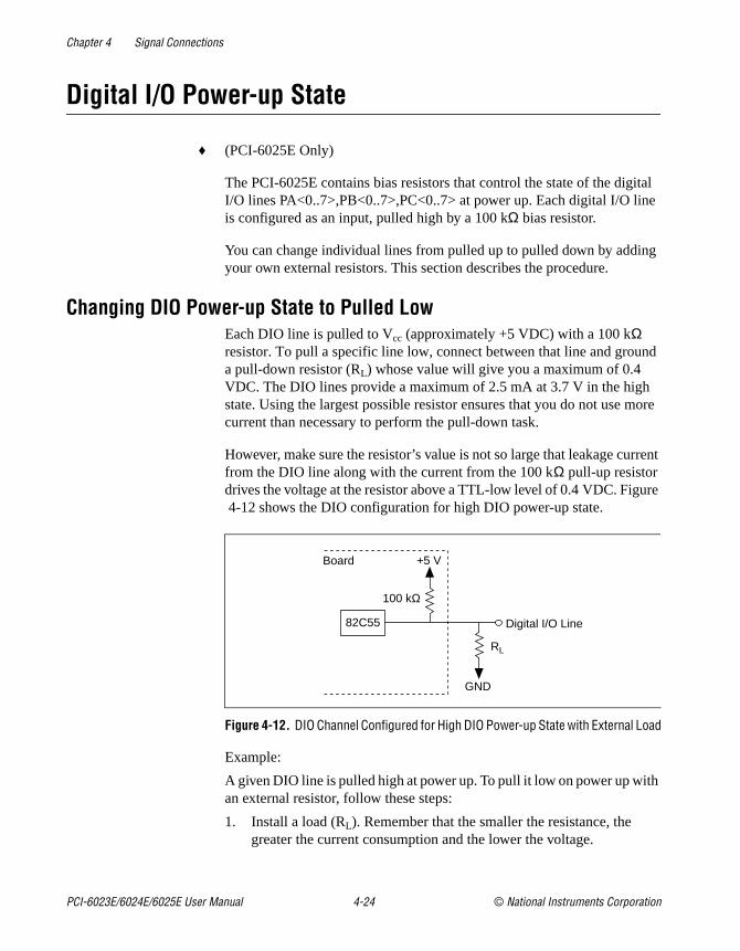
Chapter 4 Signal Connections
ital e
ng
nd
more
rrent
re
h
PCI.book Page 24 Wednesday, September 16, 1998 9:09 AM
Digital I/O Power-up State
♦ (PCI-6025E Only)
The PCI-6025E contains bias resistors that control the state of the digI/O lines PA<0..7>,PB<0..7>,PC<0..7> at power up. Each digital I/O linis configured as an input, pulled high by a 100 kΩ bias resistor.
You can change individual lines from pulled up to pulled down by addiyour own external resistors. This section describes the procedure.
Changing DIO Power-up State to Pulled LowEach DIO line is pulled to Vcc (approximately +5 VDC) with a 100 kΩ resistor. To pull a specific line low, connect between that line and groua pull-down resistor (RL) whose value will give you a maximum of 0.4 VDC. The DIO lines provide a maximum of 2.5 mA at 3.7 V in the highstate. Using the largest possible resistor ensures that you do not use current than necessary to perform the pull-down task.
However, make sure the resistor’s value is not so large that leakage cufrom the DIO line along with the current from the 100 kΩ pull-up resistor drives the voltage at the resistor above a TTL-low level of 0.4 VDC. Figu4-12 shows the DIO configuration for high DIO power-up state.
Figure 4-12. DIO Channel Configured for High DIO Power-up State with External Load
Example:
A given DIO line is pulled high at power up. To pull it low on power up witan external resistor, follow these steps:
1. Install a load (RL). Remember that the smaller the resistance, the greater the current consumption and the lower the voltage.
Board
Digital I/O Line82C55
100 kΩ
GND
RL
+5 V
PCI-6023E/6024E/6025E User Manual 4-24 © National Instruments Corporation

Chapter 4 Signal Connections
tage
er f
the
o
es
PCI.book Page 25 Wednesday, September 16, 1998 9:09 AM
2. Using the following formula, calculate the largest possible load to maintain a logic low level of 0.4 V and supply the maximum drivingcurrent:
V = I * RL ⇒ RL = V/I, where:
V = 0.4 V ; Voltage across RL
I = 46 µA + 10 µA ; 4.6 V across the 100 kΩ pull-up resistorand 10 µA maximum leakage current
Therefore:
RL = 7.1 kΩ ; 0.4 V/56 µA
This resistor value, 7.1 kΩ, provides a maximum of 0.4 V on the DIO lineat power up. You can substitute smaller resistor values to lower the volor to provide a margin for Vcc variations and other factors. However, smaller values will draw more current, leaving less drive current for othcircuitry connected to this line. The 7.1 kΩ resistor reduces the amount ologic high source current by 0.4 mA with a 2.8 V output.
Timing Specifications
♦ (PCI-6025E Only)
This section lists the timing specifications for handshaking with your PCI-6025E PC<0..7> lines. The handshaking lines STB* and IBF synchronize input transfers. The handshaking lines OBF* and ACK* synchronize output transfers. Table 4-4 describes signals appearing inhandshaking diagrams.
Table 4-4. Signal Names Used in Timing Diagrams
Name Type Description
STB* Input Strobe Input—A low signal on this handshaking line loads data intthe input latch.
IBF Output Input Buffer Full—A high signal on this handshaking line indicatesthat data has been loaded into the input latch. A low signal indicatthe board is ready for more data. This is an input acknowledge signal.
© National Instruments Corporation 4-25 PCI-6023E/6024E/6025E User Manual
Chapter 4 Signal Connections
s s
t
lid.
PCI.book Page 26 Wednesday, September 16, 1998 9:09 AM
ACK* Input Acknowledge Input—A low signal on this handshaking line indicates that the data written to the port has been accepted. Thisignal is a response from the external device indicating that it hareceived the data from your DIO board.
OBF* Output Output Buffer Full—A low signal on this handshaking line indicates that data has been written to the port.
INTR Output Interrupt Request—This signal becomes high when the 82C55Arequests service during a data transfer. The appropriate interrupenable bits must be set to generate this signal.
RD* Internal Read—This signal is the read signal generated from the control lines of the computer I/O expansion bus.
WR* Internal Write—This signal is the write signal generated from the control lines of the computer I/O expansion bus.
DATA Bidirectional Data Lines at the Specified Port—For output mode, this signal indicates the availability of data on the data line. For input mode,this signal indicates when the data on the data lines should be va
Table 4-4. Signal Names Used in Timing Diagrams (Continued)
Name Type Description
PCI-6023E/6024E/6025E User Manual 4-26 © National Instruments Corporation
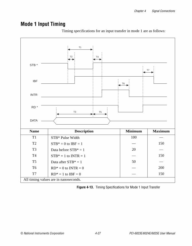
Chapter 4 Signal Connections
PCI.book Page 27 Wednesday, September 16, 1998 9:09 AM
Mode 1 Input TimingTiming specifications for an input transfer in mode 1 are as follows:
Figure 4-13. Timing Specifications for Mode 1 Input Transfer
Name Description Minimum Maximum
T1 STB* Pulse Width 100 —
T2 STB* = 0 to IBF = 1 — 150
T3 Data before STB* = 1 20 —
T4 STB* = 1 to INTR = 1 — 150
T5 Data after STB* = 1 50 —
T6 RD* = 0 to INTR = 0 — 200
T7 RD* = 1 to IBF = 0 — 150
All timing values are in nanoseconds.
DATA
RD *
INTR
IBF
STB *
T1
T2 T4
T7
T6
T3 T5
© National Instruments Corporation 4-27 PCI-6023E/6024E/6025E User Manual

Chapter 4 Signal Connections
PCI.book Page 28 Wednesday, September 16, 1998 9:09 AM
Mode 1 Output TimingTiming specifications for an output transfer in mode 1 are as follows:
Figure 4-14. Timing Specifications for Mode 1 Output Transfer
Name Description Minimum Maximum
T1 WR* = 0 to INTR = 0 — 250
T2 WR* = 1 to Output — 200
T3 WR* = 1 to OBF* = 0 — 150
T4 ACK* = 0 to OBF* = 1 — 150
T5 ACK* Pulse Width 100 —
T6 ACK* = 1 to INTR = 1 — 150
All timing values are in nanoseconds.
WR*
OBF*
INTR
ACK*
DATA
T1
T2
T3
T4
T5
T6
PCI-6023E/6024E/6025E User Manual 4-28 © National Instruments Corporation

Chapter 4 Signal Connections
ws:
PCI.book Page 29 Wednesday, September 16, 1998 9:09 AM
Mode 2 Bidirectional TimingTiming specifications for a bidirectional transfer in mode 2 are as follo
Figure 4-15. Timing Specifications for Mode 2 Bidirectional Transfer
Name Description Minimum Maximum
T1 WR* = 1 to OBF* = 0 — 150
T2 Data before STB* = 1 20 —
T3 STB* Pulse Width 100 —
T4 STB* = 0 to IBF = 1 — 150
T5 Data after STB* = 1 50 —
T6 ACK* = 0 to OBF* = 1 — 150
T7 ACK* Pulse Width 100 —
T8 ACK* = 0 to Output — 150
T9 ACK* = 1 to Output Float 20 250
T10 RD* = 1 to IBF = 0 — 150
All timing values are in nanoseconds.
T1
T6
T7
T3
T4T10
T2 T5 T8 T9
WR *
OBF *
INTR
ACK *
STB *
IBF
RD *
DATA
© National Instruments Corporation 4-29 PCI-6023E/6024E/6025E User Manual
Chapter 4 Signal Connections
a e y.
er ts
n
10
n, puts
the
al
PCI.book Page 30 Wednesday, September 16, 1998 9:09 AM
Power ConnectionsTwo pins on the I/0 connector supply +5 V from the computer power supply via a self-resetting fuse. The fuse will reset automatically withinfew seconds after the overcurrent condition is removed. These pins arreferenced to DGND and can be used to power external digital circuitr
• Power rating +4.65 to +5.25 VDC at 1 A
Caution Under no circumstances should you connect these +5 V power pins directly toanalog or digital ground or to any other voltage source on the board or any othdevice. Doing so can damage the board and the computer. National Instrumenis NOT liable for damages resulting from such a connection.
Timing ConnectionsCaution Exceeding the maximum input voltage ratings, which are listed in Table 4-2, ca
damage the board and the computer. National Instruments is NOT liable for any damages resulting from such signal connections.
All external control over the timing of your board is routed through the programmable function inputs labeled PFI<0..9>. These signals are explained in detail in the section, Programmable Function Input Connections. These PFIs are bidirectional; as outputs they are not programmable and reflect the state of many DAQ, waveform generatioand general-purpose timing signals. There are five other dedicated outfor the remainder of the timing signals. As inputs, the PFI signals are programmable and can control any DAQ, waveform generation, and general-purpose timing signals.
The DAQ signals are explained in the DAQ Timing Connections section later in this chapter. The waveform generation signals are explained in Waveform Generation Timing Connections section later in this chapter. The general-purpose timing signals are explained in the General-Purpose Timing Signal Connections section in this chapter.
All digital timing connections are referenced to DGND. This referenceis demonstrated in Figure 4-16, which shows how to connect an externTRIG1 source and an external CONVERT* source to two PCI E Seriesboard PFI pins.
!
!
PCI-6023E/6024E/6025E User Manual 4-30 © National Instruments Corporation
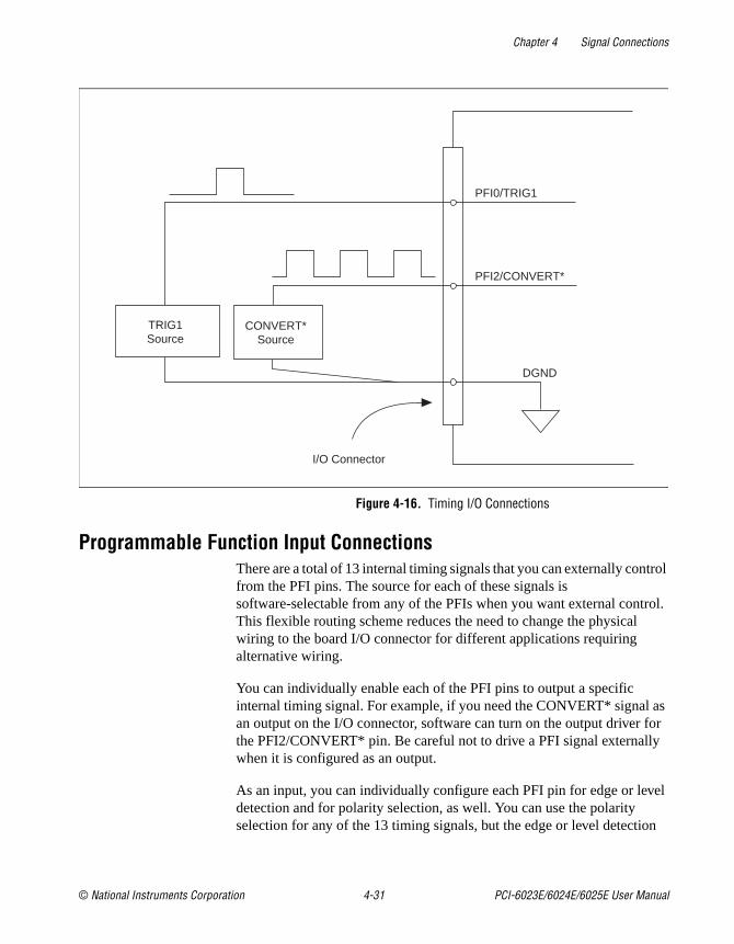
Chapter 4 Signal Connections
trol
rol.
as for y
el
n
PCI.book Page 31 Wednesday, September 16, 1998 9:09 AM
Figure 4-16. Timing I/O Connections
Programmable Function Input ConnectionsThere are a total of 13 internal timing signals that you can externally confrom the PFI pins. The source for each of these signals is software-selectable from any of the PFIs when you want external contThis flexible routing scheme reduces the need to change the physicalwiring to the board I/O connector for different applications requiring alternative wiring.
You can individually enable each of the PFI pins to output a specific internal timing signal. For example, if you need the CONVERT* signal an output on the I/O connector, software can turn on the output driver the PFI2/CONVERT* pin. Be careful not to drive a PFI signal externallwhen it is configured as an output.
As an input, you can individually configure each PFI pin for edge or levdetection and for polarity selection, as well. You can use the polarity selection for any of the 13 timing signals, but the edge or level detectio
TRIG1Source
DGND
PFI0/TRIG1
PFI2/CONVERT*
CONVERT*Source
I/O Connector
© National Instruments Corporation 4-31 PCI-6023E/6024E/6025E User Manual
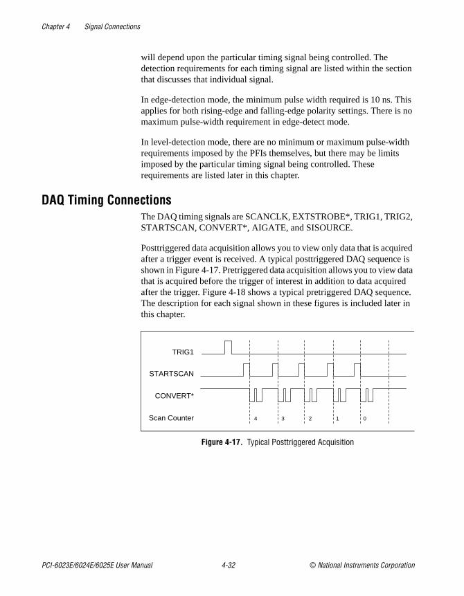
Chapter 4 Signal Connections
ion
his no
th s
,
ired is ata d ce. r in
PCI.book Page 32 Wednesday, September 16, 1998 9:09 AM
will depend upon the particular timing signal being controlled. The detection requirements for each timing signal are listed within the sectthat discusses that individual signal.
In edge-detection mode, the minimum pulse width required is 10 ns. Tapplies for both rising-edge and falling-edge polarity settings. There ismaximum pulse-width requirement in edge-detect mode.
In level-detection mode, there are no minimum or maximum pulse-widrequirements imposed by the PFIs themselves, but there may be limitimposed by the particular timing signal being controlled. These requirements are listed later in this chapter.
DAQ Timing ConnectionsThe DAQ timing signals are SCANCLK, EXTSTROBE*, TRIG1, TRIG2STARTSCAN, CONVERT*, AIGATE, and SISOURCE.
Posttriggered data acquisition allows you to view only data that is acquafter a trigger event is received. A typical posttriggered DAQ sequenceshown in Figure 4-17. Pretriggered data acquisition allows you to view dthat is acquired before the trigger of interest in addition to data acquireafter the trigger. Figure 4-18 shows a typical pretriggered DAQ sequenThe description for each signal shown in these figures is included latethis chapter.
Figure 4-17. Typical Posttriggered Acquisition
13 04 2
TRIG1
STARTSCAN
CONVERT*
Scan Counter
PCI-6023E/6024E/6025E User Manual 4-32 © National Instruments Corporation
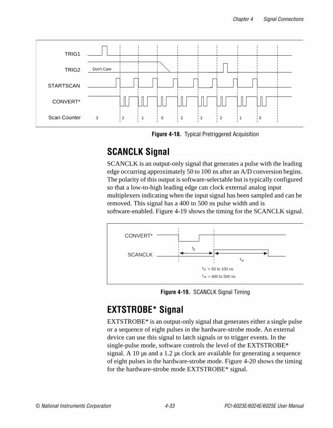
Chapter 4 Signal Connections
ing ins. ed
n be
.
lse al
nce ing
PCI.book Page 33 Wednesday, September 16, 1998 9:09 AM
Figure 4-18. Typical Pretriggered Acquisition
SCANCLK SignalSCANCLK is an output-only signal that generates a pulse with the leadedge occurring approximately 50 to 100 ns after an A/D conversion begThe polarity of this output is software-selectable but is typically configurso that a low-to-high leading edge can clock external analog input multiplexers indicating when the input signal has been sampled and caremoved. This signal has a 400 to 500 ns pulse width and is software-enabled. Figure 4-19 shows the timing for the SCANCLK signal
Figure 4-19. SCANCLK Signal Timing
EXTSTROBE* SignalEXTSTROBE* is an output-only signal that generates either a single puor a sequence of eight pulses in the hardware-strobe mode. An externdevice can use this signal to latch signals or to trigger events. In the single-pulse mode, software controls the level of the EXTSTROBE* signal. A 10 µs and a 1.2 µs clock are available for generating a sequeof eight pulses in the hardware-strobe mode. Figure 4-20 shows the timfor the hardware-strobe mode EXTSTROBE* signal.
Don't Care
0 123 1 02 2 2
TRIG1
TRIG2
STARTSCAN
CONVERT*
Scan Counter
tw
tw = 400 to 500 ns
td = 50 to 100 ns
td
CONVERT*
SCANCLK
© National Instruments Corporation 4-33 PCI-6023E/6024E/6025E User Manual
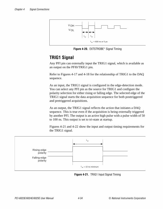
Chapter 4 Signal Connections
s
Q
e. the ed
red 50
r
PCI.book Page 34 Wednesday, September 16, 1998 9:09 AM
Figure 4-20. EXTSTROBE* Signal Timing
TRIG1 SignalAny PFI pin can externally input the TRIG1 signal, which is available aan output on the PFI0/TRIG1 pin.
Refer to Figures 4-17 and 4-18 for the relationship of TRIG1 to the DAsequence.
As an input, the TRIG1 signal is configured in the edge-detection modYou can select any PFI pin as the source for TRIG1 and configure thepolarity selection for either rising or falling edge. The selected edge ofTRIG1 signal starts the data acquisition sequence for both posttriggerand pretriggered acquisitions.
As an output, the TRIG1 signal reflects the action that initiates a DAQ sequence. This is true even if the acquisition is being externally triggeby another PFI. The output is an active high pulse with a pulse width ofto 100 ns. This output is set to tri-state at startup.
Figures 4-21 and 4-22 show the input and output timing requirements fothe TRIG1 signal.
Figure 4-21. TRIG1 Input Signal Timing
t w t w
V OH
V OL
t w = 600 ns or 5 µs
Rising-edgepolarity
Falling-edgepolarity
t w
t w = 10 ns minimum
PCI-6023E/6024E/6025E User Manual 4-34 © National Instruments Corporation
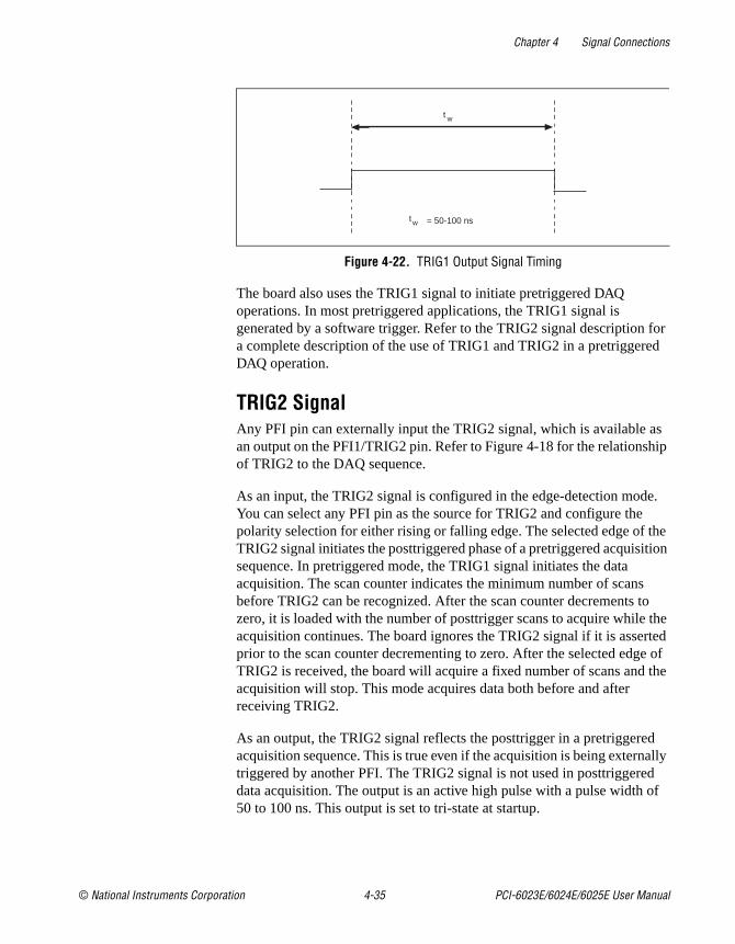
Chapter 4 Signal Connections
for ed
s hip
e. the ition
to the rted e of the
d ally d of
PCI.book Page 35 Wednesday, September 16, 1998 9:09 AM
Figure 4-22. TRIG1 Output Signal Timing
The board also uses the TRIG1 signal to initiate pretriggered DAQ operations. In most pretriggered applications, the TRIG1 signal is generated by a software trigger. Refer to the TRIG2 signal descriptiona complete description of the use of TRIG1 and TRIG2 in a pretriggerDAQ operation.
TRIG2 SignalAny PFI pin can externally input the TRIG2 signal, which is available aan output on the PFI1/TRIG2 pin. Refer to Figure 4-18 for the relationsof TRIG2 to the DAQ sequence.
As an input, the TRIG2 signal is configured in the edge-detection modYou can select any PFI pin as the source for TRIG2 and configure thepolarity selection for either rising or falling edge. The selected edge of TRIG2 signal initiates the posttriggered phase of a pretriggered acquissequence. In pretriggered mode, the TRIG1 signal initiates the data acquisition. The scan counter indicates the minimum number of scansbefore TRIG2 can be recognized. After the scan counter decrements zero, it is loaded with the number of posttrigger scans to acquire whileacquisition continues. The board ignores the TRIG2 signal if it is asseprior to the scan counter decrementing to zero. After the selected edgTRIG2 is received, the board will acquire a fixed number of scans andacquisition will stop. This mode acquires data both before and after receiving TRIG2.
As an output, the TRIG2 signal reflects the posttrigger in a pretriggereacquisition sequence. This is true even if the acquisition is being externtriggered by another PFI. The TRIG2 signal is not used in posttriggeredata acquisition. The output is an active high pulse with a pulse width 50 to 100 ns. This output is set to tri-state at startup.
t w
tw = 50-100 ns
© National Instruments Corporation 4-35 PCI-6023E/6024E/6025E User Manual

Chapter 4 Signal Connections
for
-17
n
at red e start
PCI.book Page 36 Wednesday, September 16, 1998 9:09 AM
Figures 4-23 and 4-24 show the input and output timing requirements the TRIG2 signal.
Figure 4-23. TRIG2 Input Signal Timing
Figure 4-24. TRIG2 Output Signal Timing
STARTSCAN SignalAny PFI pin can externally input the STARTSCAN signal, which is available as an output on the PFI7/STARTSCAN pin. Refer to Figures 4and 4-18 for the relationship of STARTSCAN to the DAQ sequence.
As an input, the STARTSCAN signal is configured in the edge-detectiomode. You can select any PFI pin as the source for STARTSCAN andconfigure the polarity selection for either rising or falling edge. The selected edge of the STARTSCAN signal initiates a scan. The sampleinterval counter starts if you select internally triggered CONVERT*.
As an output, the STARTSCAN signal reflects the actual start pulse thinitiates a scan. This is true even if the starts are being externally triggeby another PFI. You have two output options. The first is an active highpulse with a pulse width of 50 to 100 ns, which indicates the start of thscan. The second action is an active high pulse that terminates at the of the last conversion in the scan, which indicates a scan in progress.
Rising-edgepolarity
Falling-edgepolarity
t w
t w = 10 ns minimum
t w
tw = 50-100 ns
PCI-6023E/6024E/6025E User Manual 4-36 © National Instruments Corporation

Chapter 4 Signal Connections
s
for
the
lse
PCI.book Page 37 Wednesday, September 16, 1998 9:09 AM
STARTSCAN will be deasserted toff after the last conversion in the scan iinitiated. This output is set to tri-state at startup.
Figures 4-25 and 4-26 show the input and output timing requirements the STARTSCAN signal.
Figure 4-25. STARTSCAN Input Signal Timing
Figure 4-26. STARTSCAN Output Signal Timing
The CONVERT* pulses are masked off until the board generates the STARTSCAN signal. If you are using internally generated conversions,first CONVERT* appears when the onboard sample interval counter reaches zero. If you select an external CONVERT*, the first external puafter STARTSCAN generates a conversion. The STARTSCAN pulses should be separated by at least one scan period.
Rising-edgepolarity
Falling-edgepolarity
t w
t w = 10 ns minimum
tw = 50-100 ns
a. Start of Scan
tofftoff = 10 ns minimum
Start Pulse
CONVERT*
STARTSCAN
STARTSCAN
b. Scan in Progress, Two Conversions per Scan
tw
© National Instruments Corporation 4-37 PCI-6023E/6024E/6025E User Manual

Chapter 4 Signal Connections
ter.
are thin l or
e
is om y at
hat
with
for
PCI.book Page 38 Wednesday, September 16, 1998 9:09 AM
A counter on your board internally generates the STARTSCAN signal unless you select some external source. This counter is started by theTRIG1 signal and is stopped either by software or by the sample coun
Scans generated by either an internal or external STARTSCAN signalinhibited unless they occur within a DAQ sequence. Scans occurring wia DAQ sequence may be gated by either the hardware (AIGATE) signasoftware command register gate.
CONVERT* SignalAny PFI pin can externally input the CONVERT* signal, which is available as an output on the PFI2/CONVERT* pin.
Refer to Figures 4-17 and 4-18 for the relationship of CONVERT* to thDAQ sequence.
As an input, the CONVERT* signal is configured in the edge-detectionmode. You can select any PFI pin as the source for CONVERT* and configure the polarity selection for either rising or falling edge. The selected edge of the CONVERT* signal initiates an A/D conversion.
The ADC switches to hold mode within 60 ns of the selected edge. Thhold-mode delay time is a function of temperature and does not vary frone conversion to the next. CONVERT* pulses should be separated bleast 5 µs (200 kHz sample rate)
As an output, the CONVERT* signal reflects the actual convert pulse tis connected to the ADC. This is true even if the conversions are beingexternally generated by another PFI. The output is an active low pulse a pulse width of 50 to 150 ns. This output is set to tri-state at startup.
Figures 4-27 and 4-28 show the input and output timing requirements the CONVERT* signal.
Figure 4-27. CONVERT* Input Signal Timing
Rising-edgepolarity
Falling-edgepolarity
t w
t w = 10 ns minimum
PCI-6023E/6024E/6025E User Manual 4-38 © National Instruments Corporation
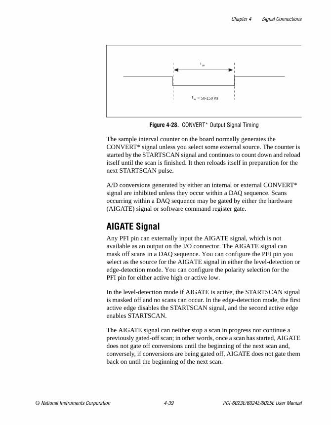
Chapter 4 Signal Connections
er is load e
*
e
u or
al first dge
ATE , em
PCI.book Page 39 Wednesday, September 16, 1998 9:09 AM
Figure 4-28. CONVERT* Output Signal Timing
The sample interval counter on the board normally generates the CONVERT* signal unless you select some external source. The countstarted by the STARTSCAN signal and continues to count down and reitself until the scan is finished. It then reloads itself in preparation for thnext STARTSCAN pulse.
A/D conversions generated by either an internal or external CONVERTsignal are inhibited unless they occur within a DAQ sequence. Scans occurring within a DAQ sequence may be gated by either the hardwar(AIGATE) signal or software command register gate.
AIGATE SignalAny PFI pin can externally input the AIGATE signal, which is not available as an output on the I/O connector. The AIGATE signal can mask off scans in a DAQ sequence. You can configure the PFI pin yoselect as the source for the AIGATE signal in either the level-detectionedge-detection mode. You can configure the polarity selection for the PFI pin for either active high or active low.
In the level-detection mode if AIGATE is active, the STARTSCAN signis masked off and no scans can occur. In the edge-detection mode, theactive edge disables the STARTSCAN signal, and the second active eenables STARTSCAN.
The AIGATE signal can neither stop a scan in progress nor continue apreviously gated-off scan; in other words, once a scan has started, AIGdoes not gate off conversions until the beginning of the next scan andconversely, if conversions are being gated off, AIGATE does not gate thback on until the beginning of the next scan.
t w
tw = 50-150 ns
© National Instruments Corporation 4-39 PCI-6023E/6024E/6025E User Manual
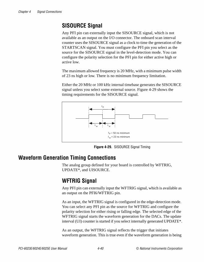
Chapter 4 Signal Connections
l f the
th
CE
as
de. e
the ate E*.
ing
PCI.book Page 40 Wednesday, September 16, 1998 9:09 AM
SISOURCE SignalAny PFI pin can externally input the SISOURCE signal, which is not available as an output on the I/O connector. The onboard scan intervacounter uses the SISOURCE signal as a clock to time the generation oSTARTSCAN signal. You must configure the PFI pin you select as thesource for the SISOURCE signal in the level-detection mode. You canconfigure the polarity selection for the PFI pin for either active high or active low.
The maximum allowed frequency is 20 MHz, with a minimum pulse widof 23 ns high or low. There is no minimum frequency limitation.
Either the 20 MHz or 100 kHz internal timebase generates the SISOURsignal unless you select some external source. Figure 4-29 shows thetiming requirements for the SISOURCE signal.
Figure 4-29. SISOURCE Signal Timing
Waveform Generation Timing ConnectionsThe analog group defined for your board is controlled by WFTRIG, UPDATE*, and UISOURCE.
WFTRIG SignalAny PFI pin can externally input the WFTRIG signal, which is availablean output on the PFI6/WFTRIG pin.
As an input, the WFTRIG signal is configured in the edge-detection moYou can select any PFI pin as the source for WFTRIG and configure thpolarity selection for either rising or falling edge. The selected edge of WFTRIG signal starts the waveform generation for the DACs. The updinterval (UI) counter is started if you select internally generated UPDAT
As an output, the WFTRIG signal reflects the trigger that initiates waveform generation. This is true even if the waveform generation is be
t p
t w t w
t p
t w
= 50 ns minimum
= 23 ns minimum
PCI-6023E/6024E/6025E User Manual 4-40 © National Instruments Corporation

Chapter 4 Signal Connections
ith
for
le
de. the the
t is nally se
PCI.book Page 41 Wednesday, September 16, 1998 9:09 AM
externally triggered by another PFI. The output is an active high pulse wa pulse width of 50 to 100 ns. This output is set to tri-state at startup.
Figures 4-30 and 4-31 show the input and output timing requirements the WFTRIG signal.
Figure 4-30. WFTRIG Input Signal Timing
Figure 4-31. WFTRIG Output Signal Timing
UPDATE* SignalAny PFI pin can externally input the UPDATE* signal, which is availabas an output on the PFI5/UPDATE* pin.
As an input, the UPDATE* signal is configured in the edge-detection moYou can select any PFI pin as the source for UPDATE* and configure polarity selection for either rising or falling edge. The selected edge of UPDATE* signal updates the outputs of the DACs. In order to use UPDATE*, you must set the DACs to posted-update mode.
As an output, the UPDATE* signal reflects the actual update pulse thaconnected to the DACs. This is true even if the updates are being extergenerated by another PFI. The output is an active low pulse with a pulwidth of 300 to 350 ns. This output is set to tri-state at startup.
Rising-edgepolarity
Falling-edgepolarity
t w
t w = 10 ns minimum
t w
tw = 50-100 ns
© National Instruments Corporation 4-41 PCI-6023E/6024E/6025E User Manual
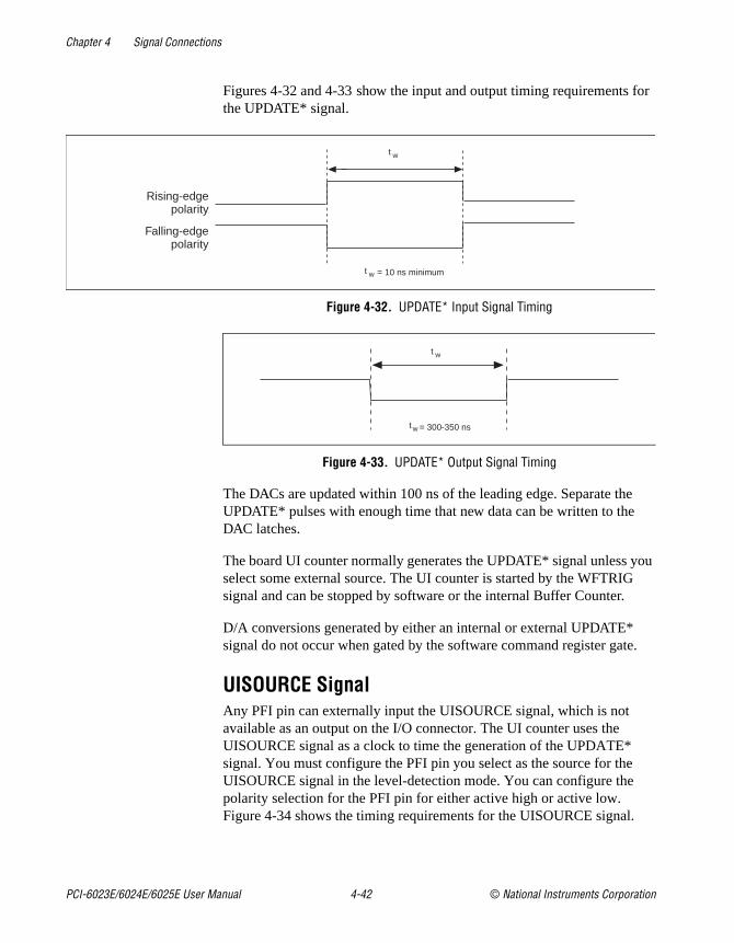
Chapter 4 Signal Connections
r
e
ou
e.
PCI.book Page 42 Wednesday, September 16, 1998 9:09 AM
Figures 4-32 and 4-33 show the input and output timing requirements fothe UPDATE* signal.
Figure 4-32. UPDATE* Input Signal Timing
Figure 4-33. UPDATE* Output Signal Timing
The DACs are updated within 100 ns of the leading edge. Separate thUPDATE* pulses with enough time that new data can be written to theDAC latches.
The board UI counter normally generates the UPDATE* signal unless yselect some external source. The UI counter is started by the WFTRIGsignal and can be stopped by software or the internal Buffer Counter.
D/A conversions generated by either an internal or external UPDATE*signal do not occur when gated by the software command register gat
UISOURCE SignalAny PFI pin can externally input the UISOURCE signal, which is not available as an output on the I/O connector. The UI counter uses the UISOURCE signal as a clock to time the generation of the UPDATE* signal. You must configure the PFI pin you select as the source for theUISOURCE signal in the level-detection mode. You can configure thepolarity selection for the PFI pin for either active high or active low. Figure 4-34 shows the timing requirements for the UISOURCE signal.
Rising-edgepolarity
Falling-edgepolarity
t w
t w = 10 ns minimum
t w
t w = 300-350 ns
PCI-6023E/6024E/6025E User Manual 4-42 © National Instruments Corporation

Chapter 4 Signal Connections
th
e
is
g
FI
PCI.book Page 43 Wednesday, September 16, 1998 9:09 AM
Figure 4-34. UISOURCE Signal Timing
The maximum allowed frequency is 20 MHz, with a minimum pulse widof 23 ns high or low. There is no minimum frequency limitation.
Either the 20 MHz or 100 kHz internal timebase normally generates thUISOURCE signal unless you select some external source.
General-Purpose Timing Signal ConnectionsThe general-purpose timing signals are GPCTR0_SOURCE, GPCTR0_GATE, GPCTR0_OUT, GPCTR0_UP_DOWN, GPCTR1_SOURCE, GPCTR1_GATE, GPCTR1_OUT, GPCTR1_UP_DOWN, and FREQ_OUT.
GPCTR0_SOURCE SignalAny PFI pin can externally input the GPCTR0_SOURCE signal, whichavailable as an output on the PFI8/GPCTR0_SOURCE pin.
As an input, the GPCTR0_SOURCE signal is configured in the edge-detection mode. You can select any PFI pin as the source for GPCTR0_SOURCE and configure the polarity selection for either risinor falling edge.
As an output, the GPCTR0_SOURCE signal reflects the actual clock connected to general-purpose counter 0. This is true even if another Pis externally inputting the source clock. This output is set to tri-state atstartup.
Figure 4-35 shows the timing requirements for the GPCTR0_SOURCEsignal.
t p
t w t w
t p
t w
= 50 ns minimum
= 23 ns minimum
© National Instruments Corporation 4-43 PCI-6023E/6024E/6025E User Manual

Chapter 4 Signal Connections
th
tion nd se
uch
l s e at
PCI.book Page 44 Wednesday, September 16, 1998 9:09 AM
Figure 4-35. GPCTR0_SOURCE Signal Timing
The maximum allowed frequency is 20 MHz, with a minimum pulse widof 23 ns high or low. There is no minimum frequency limitation.
The 20 MHz or 100 kHz timebase normally generates the GPCTR0_SOURCE signal unless you select some external source.
GPCTR0_GATE SignalAny PFI pin can externally input the GPCTR0_GATE signal, which is available as an output on the PFI9/GPCTR0_GATE pin.
As an input, the GPCTR0_GATE signal is configured in the edge-detecmode. You can select any PFI pin as the source for GPCTR0_GATE aconfigure the polarity selection for either rising or falling edge. You can uthe gate signal in a variety of different applications to perform actions sas starting and stopping the counter, generating interrupts, saving thecounter contents, and so on.
As an output, the GPCTR0_GATE signal reflects the actual gate signaconnected to general-purpose counter 0. This is true even if the gate ibeing externally generated by another PFI. This output is set to tri-statstartup.
t p
t w t w
t p
t w
= 50 ns minimum
= 23 ns minimum
PCI-6023E/6024E/6025E User Manual 4-44 © National Instruments Corporation
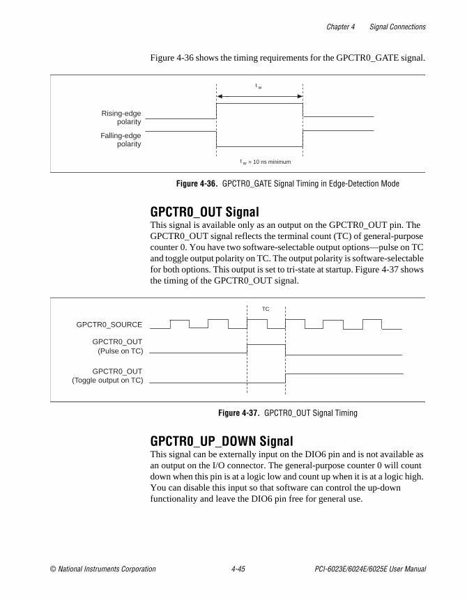
Chapter 4 Signal Connections
nal.
he se
TC ble ows
as unt gh.
PCI.book Page 45 Wednesday, September 16, 1998 9:09 AM
Figure 4-36 shows the timing requirements for the GPCTR0_GATE sig
Figure 4-36. GPCTR0_GATE Signal Timing in Edge-Detection Mode
GPCTR0_OUT SignalThis signal is available only as an output on the GPCTR0_OUT pin. TGPCTR0_OUT signal reflects the terminal count (TC) of general-purpocounter 0. You have two software-selectable output options—pulse onand toggle output polarity on TC. The output polarity is software-selectafor both options. This output is set to tri-state at startup. Figure 4-37 shthe timing of the GPCTR0_OUT signal.
Figure 4-37. GPCTR0_OUT Signal Timing
GPCTR0_UP_DOWN SignalThis signal can be externally input on the DIO6 pin and is not availablean output on the I/O connector. The general-purpose counter 0 will codown when this pin is at a logic low and count up when it is at a logic hiYou can disable this input so that software can control the up-down functionality and leave the DIO6 pin free for general use.
Rising-edgepolarity
Falling-edgepolarity
t w
t w = 10 ns minimum
GPCTR0_SOURCE
GPCTR0_OUT
GPCTR0_OUT(Toggle output on TC)
(Pulse on TC)
TC
© National Instruments Corporation 4-45 PCI-6023E/6024E/6025E User Manual
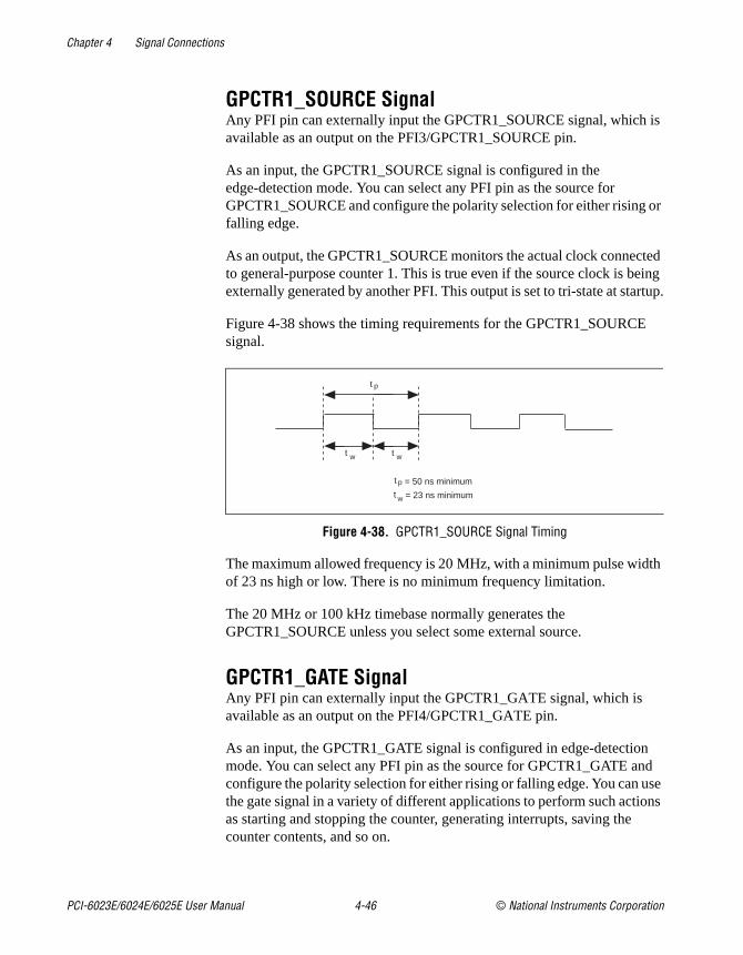
Chapter 4 Signal Connections
is
or
ted eing rtup.
th
n nd se
ons
PCI.book Page 46 Wednesday, September 16, 1998 9:09 AM
GPCTR1_SOURCE SignalAny PFI pin can externally input the GPCTR1_SOURCE signal, whichavailable as an output on the PFI3/GPCTR1_SOURCE pin.
As an input, the GPCTR1_SOURCE signal is configured in the edge-detection mode. You can select any PFI pin as the source for GPCTR1_SOURCE and configure the polarity selection for either risingfalling edge.
As an output, the GPCTR1_SOURCE monitors the actual clock connecto general-purpose counter 1. This is true even if the source clock is bexternally generated by another PFI. This output is set to tri-state at sta
Figure 4-38 shows the timing requirements for the GPCTR1_SOURCEsignal.
Figure 4-38. GPCTR1_SOURCE Signal Timing
The maximum allowed frequency is 20 MHz, with a minimum pulse widof 23 ns high or low. There is no minimum frequency limitation.
The 20 MHz or 100 kHz timebase normally generates the GPCTR1_SOURCE unless you select some external source.
GPCTR1_GATE SignalAny PFI pin can externally input the GPCTR1_GATE signal, which is available as an output on the PFI4/GPCTR1_GATE pin.
As an input, the GPCTR1_GATE signal is configured in edge-detectiomode. You can select any PFI pin as the source for GPCTR1_GATE aconfigure the polarity selection for either rising or falling edge. You can uthe gate signal in a variety of different applications to perform such actias starting and stopping the counter, generating interrupts, saving thecounter contents, and so on.
t p
t w t w
t p
t w
= 50 ns minimum
= 23 ns minimum
PCI-6023E/6024E/6025E User Manual 4-46 © National Instruments Corporation

Chapter 4 Signal Connections
al s e at
nal.
TC ble ows
as n an
PCI.book Page 47 Wednesday, September 16, 1998 9:09 AM
As an output, the GPCTR1_GATE signal monitors the actual gate signconnected to general-purpose counter 1. This is true even if the gate ibeing externally generated by another PFI. This output is set to tri-statstartup.
Figure 4-39 shows the timing requirements for the GPCTR1_GATE sig
Figure 4-39. GPCTR1_GATE Signal Timing in Edge-Detection Mode
GPCTR1_OUT SignalThis signal is available only as an output on the GPCTR1_OUT pin. The GPCTR1_OUT signal monitors the TC board general-purpose counter 1. You have two software-selectable output options—pulse onand toggle output polarity on TC. The output polarity is software-selectafor both options. This output is set to tri-state at startup. Figure 4-40 shthe timing requirements for the GPCTR1_OUT signal.
Figure 4-40. GPCTR1_OUT Signal Timing
GPCTR1_UP_DOWN SignalThis signal can be externally input on the DIO7 pin and is not availablean output on the I/O connector. General-purpose counter 1 counts dowwhen this pin is at a logic low and counts up at a logic high. This input cbe disabled so that software can control the up-down functionality and
Rising-edgepolarity
Falling-edgepolarity
t w
t w = 10 ns minimum
GPCTR1_SOURCE
GPCTR1_OUT
GPCTR1_OUT(Toggle output on TC)
(Pulse on TC)
TC
© National Instruments Corporation 4-47 PCI-6023E/6024E/6025E User Manual
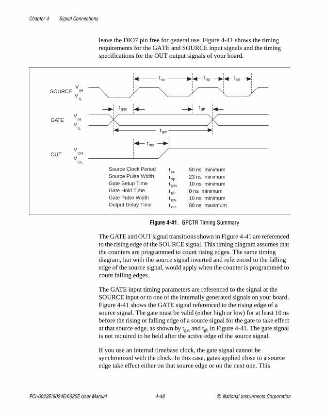
Chapter 4 Signal Connections
ced that
ng d to
ard.
ns ffect
rce
PCI.book Page 48 Wednesday, September 16, 1998 9:09 AM
leave the DIO7 pin free for general use. Figure 4-41 shows the timing requirements for the GATE and SOURCE input signals and the timingspecifications for the OUT output signals of your board.
Figure 4-41. GPCTR Timing Summary
The GATE and OUT signal transitions shown in Figure 4-41 are referento the rising edge of the SOURCE signal. This timing diagram assumesthe counters are programmed to count rising edges. The same timing diagram, but with the source signal inverted and referenced to the falliedge of the source signal, would apply when the counter is programmecount falling edges.
The GATE input timing parameters are referenced to the signal at the SOURCE input or to one of the internally generated signals on your boFigure 4-41 shows the GATE signal referenced to the rising edge of a source signal. The gate must be valid (either high or low) for at least 10before the rising or falling edge of a source signal for the gate to take eat that source edge, as shown by tgsu and tgh in Figure 4-41. The gate signalis not required to be held after the active edge of the source signal.
If you use an internal timebase clock, the gate signal cannot be synchronized with the clock. In this case, gates applied close to a souedge take effect either on that source edge or on the next one. This
SOURCEV
IHV
IL
VIH
VIL
t sc t sp
t gsu t gh
t gw
GATE
t out
OUTV
OHV
OL
sc
ttttt
t 50 ns minimum
sp 23 ns minimum
gsu 10 ns minimum
gh 0 ns minimum
gw 10 ns minimum
out 80 ns maximum
Source Clock PeriodSource Pulse WidthGate Setup TimeGate Hold TimeGate Pulse WidthOutput Delay Time
t sp
PCI-6023E/6024E/6025E User Manual 4-48 © National Instruments Corporation

Chapter 4 Signal Connections
he e of the
cy rs 1
The
ts nal
rd,
the
ut the
ing
e
PCI.book Page 49 Wednesday, September 16, 1998 9:09 AM
arrangement results in an uncertainty of one source clock period with respect to unsynchronized gating sources.
The OUT output timing parameters are referenced to the signal at theSOURCE input or to one of the internally generated clock signals on tboards. Figure 4-41 shows the OUT signal referenced to the rising edga source signal. Any OUT signal state changes occur within 80 ns afterrising or falling edge of the source signal.
FREQ_OUT SignalThis signal is available only as an output on the FREQ_OUT pin. The board’s frequency generator outputs the FREQ_OUT pin. The frequengenerator is a 4-bit counter that can divide its input clock by the numbethrough 16. The input clock of the frequency generator is software-selectable from the internal 10 MHz and 100 kHz timebases. output polarity is software-selectable. This output is set to tri-state at startup.
Field Wiring ConsiderationsEnvironmental noise can seriously affect the accuracy of measuremenmade with your board if you do not take proper care when running sigwires between signal sources and the board. The following recommendations apply mainly to analog input signal routing to the boaalthough they also apply to signal routing in general.
Minimize noise pickup and maximize measurement accuracy by takingfollowing precautions:
• Use differential analog input connections to reject common-mode noise.
• Use individually shielded, twisted-pair wires to connect analog inpsignals to the board. With this type of wire, the signals attached toCH+ and CH– inputs are twisted together and then covered with ashield. You then connect this shield only at one point to the signalsource ground. This kind of connection is required for signals travelthrough areas with large magnetic fields or high electromagnetic interference.
• Route signals to the board carefully. Keep cabling away from noissources. The most common noise source in a PCI data acquisitionsystem is the video monitor. Separate the monitor from the analogsignals as much as possible.
© National Instruments Corporation 4-49 PCI-6023E/6024E/6025E User Manual

Chapter 4 Signal Connections
r
. lines etic
they
es.
, ugh
PCI.book Page 50 Wednesday, September 16, 1998 9:09 AM
The following recommendations apply for all signal connections to youboard:
• Separate board signal lines from high-current or high-voltage linesThese lines can induce currents in or voltages on the board signal if they run in parallel paths at a close distance. To reduce the magncoupling between lines, separate them by a reasonable distance ifrun in parallel, or run the lines at right angles to each other.
• Do not run signal lines through conduits that also contain power lin
• Protect signal lines from magnetic fields caused by electric motorswelding equipment, breakers, or transformers by running them throspecial metal conduits.
For more information, refer to the application note, Field Wiring and Noise Consideration for Analog Signals, available from National Instruments.
PCI-6023E/6024E/6025E User Manual 4-50 © National Instruments Corporation
© National Instruments Corporation 5-1 PCI-6023E/6024E/60
PCI.book Page 1 Wednesday, September 16, 1998 9:09 AM
5
areut hese s
pter. ast
to
le ty, d.
Cs
to the a
into s can
Calibration
This chapter discusses the calibration procedures for your board. If youusing the NI-DAQ device driver, that software includes calibration functions for performing all of the steps in the calibration process.
Calibration refers to the process of minimizing measurement and outpvoltage errors by making small circuit adjustments. For these boards, tadjustments take the form of writing values to onboard calibration DAC(CalDACs).
Some form of board calibration is required for all but the most forgivingapplications. If you do not calibrate your board, your signals and measurements could have very large offset, gain, and linearity errors.
Three levels of calibration are available to you and described in this chaThe first level is the fastest, easiest, and least accurate, whereas the llevel is the slowest, most difficult, and most accurate.
Loading Calibration ConstantsYour board is factory calibrated before shipment at approximately 25° Cthe levels indicated in Appendix A, Specifications. The associated calibration constants—the values that were written to the CalDACs to achieve calibration in the factory—are stored in the onboard nonvolatimemory (EEPROM). Because the CalDACs have no memory capabilithey do not retain calibration information when the board is unpowereLoading calibration constants refers to the process of loading the CalDAwith the values stored in the EEPROM. NI-DAQ software determines when this is necessary and does it automatically. If you are not using NI-DAQ, you must load these values yourself.
In the EEPROM there is a user-modifiable calibration area in addition the permanent factory calibration area. This means that you can load CalDACs with values either from the original factory calibration or fromcalibration that you subsequently performed.
This method of calibration is not very accurate because it does not takeaccount the fact that the board measurement and output voltage error
25E User Manual
Chapter 5 Calibration
ard
ted nts ss,
ze to
n d h is ive
cy of
ROM t e or may
and form ard
rnal the
PCI.book Page 2 Wednesday, September 16, 1998 9:09 AM
vary with time and temperature. It is better to self-calibrate when the bois installed in the environment in which it will be used.
Self-CalibrationYour board can measure and correct for almost all of its calibration-relaerrors without any external signal connections. Your National Instrumesoftware provides a self-calibration method. This self-calibration procewhich generally takes less than a minute, is the preferred method of assuring accuracy in your application. Initiate self-calibration to minimithe effects of any offset, gain, and linearity drifts, particularly those duewarmup.
Immediately after self-calibration, the only significant residual calibratioerror could be gain error due to time or temperature drift of the onboarvoltage reference. This error is addressed by external calibration, whicdiscussed in the following section. If you are interested primarily in relatmeasurements, you can ignore a small amount of gain error, and self-calibration should be sufficient.
External CalibrationYour board has an onboard calibration reference to ensure the accuraself-calibration. Its specifications are listed in Appendix A, Specifications. The reference voltage is measured at the factory and stored in the EEPfor subsequent self-calibrations. This voltage is stable enough for mosapplications, but if you are using your board at an extreme temperaturif the onboard reference has not been measured for a year or more, youwish to externally calibrate your board.
An external calibration refers to calibrating your board with a known external reference rather than relying on the onboard reference. Redetermining the value of the onboard reference is part of this processthe results can be saved in the EEPROM, so you should not have to peran external calibration very often. You can externally calibrate your boby calling the NI-DAQ calibration function.
To externally calibrate your board, be sure to use a very accurate extereference. The reference should be several times more accurate thanboard itself.
PCI-6023E/6024E/6025E User Manual 5-2 © National Instruments Corporation
Chapter 5 Calibration
his
tput le to in
PCI.book Page 3 Wednesday, September 16, 1998 9:09 AM
Other ConsiderationsThe CalDACs adjust the gain error of each analog output channel by adjusting the value of the reference voltage supplied to that channel. Tcalibration mechanism is designed to work only with the internal 10 V reference. Thus, in general, it is not possible to calibrate the analog ougain error when using an external reference. In this case, it is advisabaccount for the nominal gain error of the analog output channel either software or with external hardware. See Appendix A, Specifications, for analog output gain error information.
© National Instruments Corporation 5-3 PCI-6023E/6024E/6025E User Manual
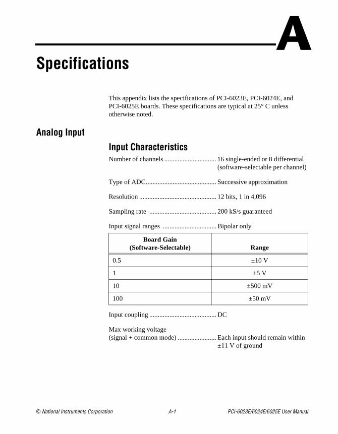
© National Instruments Corporation A-1 PCI-6023E/6024E/60
PCI.book Page 1 Wednesday, September 16, 1998 9:09 AM
A
ial )
in
Specifications
This appendix lists the specifications of PCI-6023E, PCI-6024E, and PCI-6025E boards. These specifications are typical at 25° C unless otherwise noted.
Analog Input
Input CharacteristicsNumber of channels ............................... 16 single-ended or 8 different
(software-selectable per channel
Type of ADC.......................................... Successive approximation
Resolution .............................................. 12 bits, 1 in 4,096
Sampling rate ........................................ 200 kS/s guaranteed
Input signal ranges ................................ Bipolar only
Input coupling ........................................ DC
Max working voltage(signal + common mode) ....................... Each input should remain with
±11 V of ground
Board Gain (Software-Selectable) Range
0.5 ±10 V
1 ±5 V
10 ±500 mV
100 ±50 mV
25E User Manual

Appendix A Specifications
)
rag
PCI.book Page 2 Wednesday, September 16, 1998 9:09 AM
Overvoltage protection
FIFO buffer size......................................512 S
Data transfers ..........................................DMA, interrupts, programmed I/O
DMA modes ...........................................Scatter-gather(Single transfer, demand transfer
Configuration memory size ....................512 words
Accuracy Information
♦ PCI-6025E Accuracy Information
Powered On Powered Off
ACH<0..15> ± 42 ± 35
AISENSE ± 40 ± 25
Nominal Range (V)
Absolute Accuracy Relative Accuracy
% of Reading Offset Noise + Quantization
(mV)Temp Drift Resolution (mV)
Positive FS
NegativeFS 24 Hours 90 Days 1 Year (mV) Single Pt. Averaged (%/° C) Theoretical Averaged
10 –10 0.0722 0.0742 0.0764 ± 6.385 ± 3.906 ± 0.975 0.0010 4.883 1.284
5 –5 0.0272 0.0292 0.0314 ± 3.203 ± 1.953 ± 0.488 0.0005 2.441 0.642
0.5 –0.5 0.0722 0.0742 0.0764 ± 0.340 ± 0.195 ± 0.049 0.0010 0.244 0.064
0.05 –0.05 0.0722 0.0742 0.0764 ± 0.054 ± 0.063 ± 0.006 0.0010 0.024 0.008
Note: Accuracies are valid for measurements following an internal E Series Calibration. Averaged numbers assume dithering and aveing of 100 single-channel readings. Measurement accuracies are listed for operational temperatures within ± 1 °C of internal calibration temperature and ± 10 °C of external or factory calibration temperature.
PCI-6023E/6024E/6025E User Manual A-2 © National Instruments Corporation
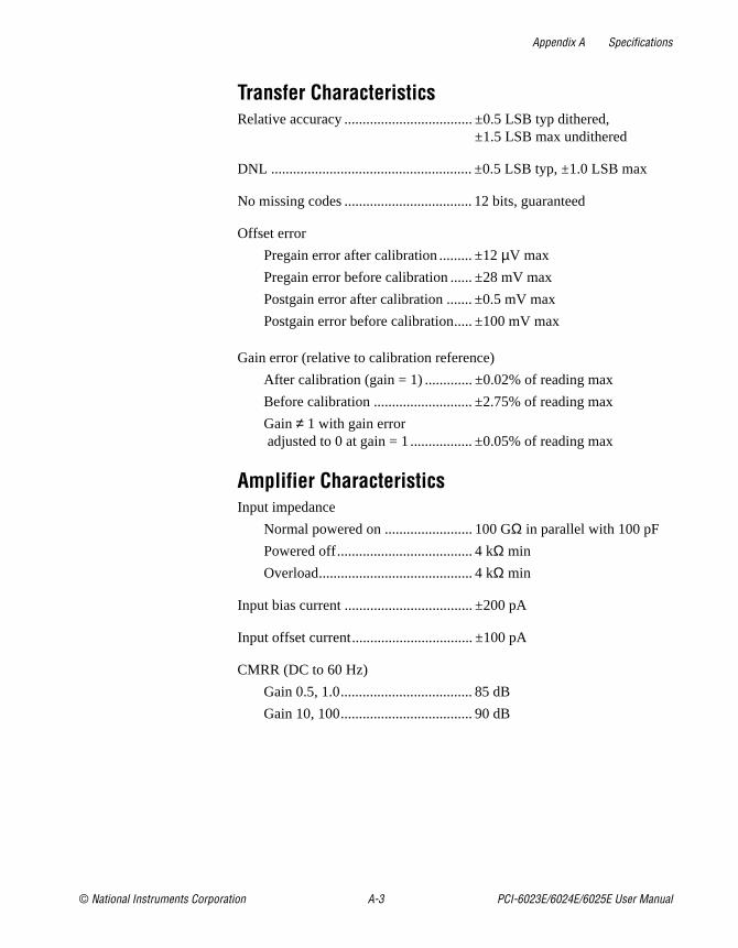
Appendix A Specifications
PCI.book Page 3 Wednesday, September 16, 1998 9:09 AM
Transfer CharacteristicsRelative accuracy ................................... ±0.5 LSB typ dithered,
±1.5 LSB max undithered
DNL ....................................................... ±0.5 LSB typ, ±1.0 LSB max
No missing codes ................................... 12 bits, guaranteed
Offset error
Pregain error after calibration ......... ±12 µV max
Pregain error before calibration ...... ±28 mV max
Postgain error after calibration ....... ±0.5 mV max
Postgain error before calibration..... ±100 mV max
Gain error (relative to calibration reference)
After calibration (gain = 1) ............. ±0.02% of reading max
Before calibration ........................... ±2.75% of reading max
Gain ≠ 1 with gain error adjusted to 0 at gain = 1 ................. ±0.05% of reading max
Amplifier CharacteristicsInput impedance
Normal powered on ........................ 100 GΩ in parallel with 100 pF
Powered off..................................... 4 kΩ min
Overload.......................................... 4 kΩ min
Input bias current ................................... ±200 pA
Input offset current................................. ±100 pA
CMRR (DC to 60 Hz)
Gain 0.5, 1.0.................................... 85 dB
Gain 10, 100.................................... 90 dB
© National Instruments Corporation A-3 PCI-6023E/6024E/6025E User Manual
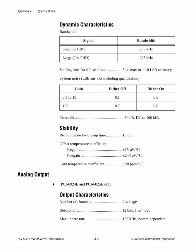
Appendix A Specifications
PCI.book Page 4 Wednesday, September 16, 1998 9:09 AM
Dynamic CharacteristicsBandwidth
Settling time for full scale step ...............5µs max to ±1.0 LSB accuracy
System noise (LSBrms, not including quantization)
Crosstalk .................................................–60 dB, DC to 100 kHz
StabilityRecommended warm-up time.................15 min.
Offset temperature coefficient
Pregain.............................................±15 µV/°C
Postgain ...........................................±240 µV/°C
Gain temperature coefficient ..................±20 ppm/°C
Analog Output
♦ (PCI-6024E and PCI-6025E only)
Output CharacteristicsNumber of channels................................2 voltage
Resolution...............................................12 bits, 1 in 4,096
Max update rate .....................................100 kHz, system dependent
Signal Bandwidth
Small (–3 dB) 500 kHz
Large (1% THD) 225 kHz
Gain Dither Off Dither On
0.5 to 10 0.1 0.6
100 0.7 0.8
PCI-6023E/6024E/6025E User Manual A-4 © National Instruments Corporation
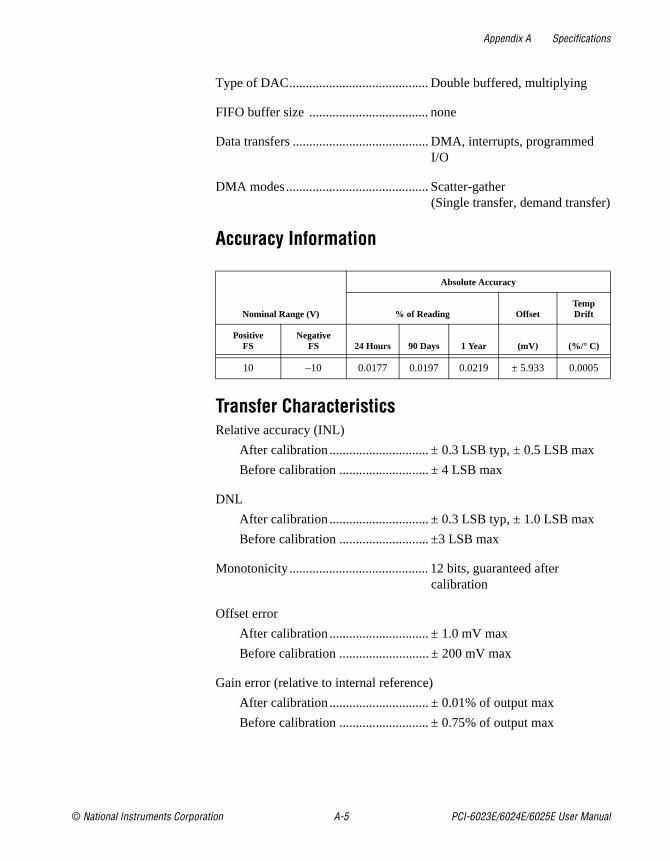
Appendix A Specifications
d
)
PCI.book Page 5 Wednesday, September 16, 1998 9:09 AM
Type of DAC.......................................... Double buffered, multiplying
FIFO buffer size .................................... none
Data transfers ......................................... DMA, interrupts, programmeI/O
DMA modes........................................... Scatter-gather(Single transfer, demand transfer
Accuracy Information
Transfer CharacteristicsRelative accuracy (INL)
After calibration.............................. ± 0.3 LSB typ, ± 0.5 LSB max
Before calibration ........................... ± 4 LSB max
DNL
After calibration.............................. ± 0.3 LSB typ, ± 1.0 LSB max
Before calibration ........................... ±3 LSB max
Monotonicity.......................................... 12 bits, guaranteed after calibration
Offset error
After calibration.............................. ± 1.0 mV max
Before calibration ........................... ± 200 mV max
Gain error (relative to internal reference)
After calibration.............................. ± 0.01% of output max
Before calibration ........................... ± 0.75% of output max
Nominal Range (V)
Absolute Accuracy
% of Reading Offset TempDrift
PositiveFS
NegativeFS 24 Hours 90 Days 1 Year (mV) (%/° C)
10 –10 0.0177 0.0197 0.0219 ± 5.933 0.0005
© National Instruments Corporation A-5 PCI-6023E/6024E/6025E User Manual

Appendix A Specifications
PCI.book Page 6 Wednesday, September 16, 1998 9:09 AM
Voltage OutputRange ......................................................± 10 V
Output coupling ......................................DC
Output impedance...................................0.1 Ω max
Current drive...........................................±5 mA max
Protection................................................Short-circuit to ground
Power-on state ........................................0 V
Dynamic CharacteristicsSettling time for full-scale step...............10 µs to ±0.5 LSB accuracy
Slew rate .................................................10 V/µs
Noise.......................................................200 µVrms, DC to 1 MHz
Glitch energy (at midscal transition)
Magnitude .............................................. ± 12 mV
Duration........................................... 2.0 µs
StabilityOffset temperature coefficient ................± 50 µV/°C
Gain temperature coefficient ..................±25 ppm /°C
Digital I/O Number of channels
PCI-6025E .......................................32 input/output
PCI-6023E and PCI-6024E .............8 input/output
Compatibility ..........................................TTL/CMOS
PCI-6023E/6024E/6025E User Manual A-6 © National Instruments Corporation

Appendix A Specifications
PCI.book Page 7 Wednesday, September 16, 1998 9:09 AM
DIO<0..7>Digital logic levels
Power-on state ........................................ Input (High-Z),50 kΩ pull up to +5VDC
Data transfers ......................................... Programmed I/O
PA<0..7>,PB<0..7>,PC<0..7>
♦ PCI-6025E only
Digital logic levels
Handshaking........................................... 2-wire
Power-on state
PA<0..7> ................................................ Input (High-Z),100 kΩ pull up to +5VDC
Level Min Max
Input low voltage
Input high voltage
Input low current (Vin = 0 V)
Input high current (Vin = 5 V)
0 V
2 V
—
—
0.8 V
5 V
–320µA
10 µA
Output low voltage (IOL = 24 mA)
Output high voltage (IOH = 13 mA)
—
4.35 V
0.4 V
—
Level Min Max
Input low voltage
Input high voltage
Input low current (Vin = 0 V, 100 kΩ pull up)
Input high current (Vin = 5 V, 100 kΩ pull up)
0 V
2.2 V
—
—
0.8 V
5 V
–75µA
10 µA
Output low voltage (IOL = 2.5 mA)
Output high voltage (IOH = 2.5 mA)
—
3.7 V
0.4 V
—
© National Instruments Corporation A-7 PCI-6023E/6024E/6025E User Manual

Appendix A Specifications
d
)
PCI.book Page 8 Wednesday, September 16, 1998 9:09 AM
PB<0..7>.................................................Input (High-Z),100 kΩ pull up to +5VDC
PC<0..7>.................................................Input (High-Z),100 kΩ pull up to +5VDC
Data transfers ..........................................Interrupts, programmed I/O
Timing I/ONumber of channels................................2 up/down counter/timers, 1
frequency scaler
Resolution...............................................
Counter/timers .................................24 bits
Frequency scalers ............................4 bits
Compatibility ..........................................TTL/CMOS
Base clocks available
Counter/timers .................................20 MHz, 100 kHz
Frequency scalers ............................10 MHz, 100 kHz
Base clock accuracy................................±0.01%
Max source frequency.............................20 MHz
Min source pulse duration ......................10 ns in edge-detect mode
Min gate pulse duration ..........................10 ns in edge-detect mode
Data transfers ..........................................DMA, interrupts, programmeI/O
DMA modes ...........................................Scatter-gather(Single transfer, demand transfer
Triggers
Digital TriggerCompatibility ..........................................TTL
Response.................................................Rising or falling edge
PCI-6023E/6024E/6025E User Manual A-8 © National Instruments Corporation
Appendix A Specifications
A
n.)
PCI.book Page 9 Wednesday, September 16, 1998 9:09 AM
Pulse width............................................. 10 ns min
RTSI
Trigger lines ........................................... 7
CalibrationInterval ................................................... 1 year
Onboard calibration reference
Level ............................................... 5.000 V (±3.5 mV) (actual value stored in EEPROM)
Temperature coefficient .................. ±5 ppm/°C max
Long-term stability ......................... ±15 ppm/
Power Requirement+5 VDC (±5%)....................................... 0.7 A
Power available at I/O connector ........... +4.65 VDC to +5.25 VDC at 1
PhysicalDimensions (not including connectors) ............................................. 17.5 by 10.6 cm (6.9 by 4.2 i
I/O connector
PCI-6023E/6024E........................... 68-pin male SCSI-II type
PCI-6025E ...................................... 100-pin female 0.05D type
Operating EnvironmentAmbient temperature.............................. 0° to 55° C
Relative humidity................................... 10% to 90% noncondensing
Storage EnvironmentAmbient temperature.............................. -20° to 70° C
Relative humidity................................... 5% to 95% noncondensing
1 000 h,
© National Instruments Corporation A-9 PCI-6023E/6024E/6025E User Manual

© National Instruments Corporation B-1 PCI-6023E/6024E/60
PCI.book Page 1 Wednesday, September 16, 1998 9:09 AM
B
thee ons.
es
d g
t
are
Custom Cabling and Optional Connectors
This appendix describes the various cabling and connector options forboards.
Custom CablingNational Instruments offers cables and accessories for you to prototypyour application or to use if you frequently change board interconnecti
If you want to develop your own cable, however, the following guidelinmay be useful:
• For the analog input signals, shielded twisted-pair wires for each analog input pair yield the best results, assuming that you use differential inputs. Tie the shield for each signal pair to the groundreference at the source.
• You should route the analog lines separately from the digital lines.
• When using a cable shield, use separate shields for the analog andigital halves of the cable. Failure to do so results in noise couplininto the analog signals from transient digital signals.
The following list gives recommended part numbers for connectors thamate to the I/O connector on your board.
Mating connectors and a backshell kit for making custom 68-pin cablesavailable from National Instruments (part number 776832-01)
♦ PCI-6023E and PCI-6024E
Honda 68-position, solder cup, female connector (part number PCS-E68FS)
Honda backshell (part number PCS-E68LKPA)
25E User Manual

Appendix B Custom Cabling and Optional Connectors
tor.
bly
PCI.book Page 2 Wednesday, September 16, 1998 9:09 AM
♦ PCI-6025E
AMP 100-position IDC male connector (part number 1-750913-9)
AMP backshell, 0.50 max O.D. cable (part number 749081-1)
AMP backshell, 0.55 max O.D. cable, (part number 749854-1)
Optional ConnectorsFigure B-1 shows the pin assignments for the 68-pin E Series connecThis connector is available when you use the SH6868 or R6868 cableassemblies with the PCI-6023E and PCI-6024E. It is also the MIO-16 68-pin connector available when you use the SH1006868 cable assemwith the PCI-6025E.
PCI-6023E/6024E/6025E User Manual B-2 © National Instruments Corporation

Appendix B Custom Cabling and Optional Connectors
PCI.book Page 3 Wednesday, September 16, 1998 9:09 AM
Figure B-1. 68-Pin E Series Connector Pin Assignments
FREQ_OUT
GPCTR0_OUT
PFI9/GPCTR0_GATE
DGND
PFI6/WFTRIG
PFI5/UPDATE*
DGND
+5 VDGND
PFI1/TRIG2
PFI0/TRIG1
DGND
DGND
+5 V
DGNDDIO6
DIO1
DGND
DIO4
RESERVED DAC1OUT1
DAC0OUT1
ACH15AIGND
ACH6ACH13
AIGND
ACH4
AIGNDACH3
ACH10
AIGND
ACH1ACH8
DGND
1 Not available on the PCI-6023E
PFI8/GPCTR0_SOURCE
PFI7/STARTSCAN
GPCTR1_OUT
PFI4/GPCTR1_GATE
PFI3/GPCTR1_SOURCE
PFI2/CONVERT*
DGND
DGND
DGND
EXTSTROBE*
SCANCLK
DIO3
DIO7
DIO2DGND
DIO5
DIO0
DGND
AOGND
AOGND
AIGND
ACH7
ACH14
AIGND
ACH5
ACH12
AISENSE
ACH11
AIGND
ACH2
ACH9
AIGNDACH0
1 35
2 36
3 37
4 38
5 39
6 40
7 41
8 42
9 43
10 44
11 45
12 46
13 47
14 48
15 49
16 50
17 51
18 52
19 53
20 54
21 55
22 56
23 57
24 58
25 59
26 60
27 61
28 62
29 63
30 64
31 65
32 66
33 67
34 68
© National Instruments Corporation B-3 PCI-6023E/6024E/6025E User Manual
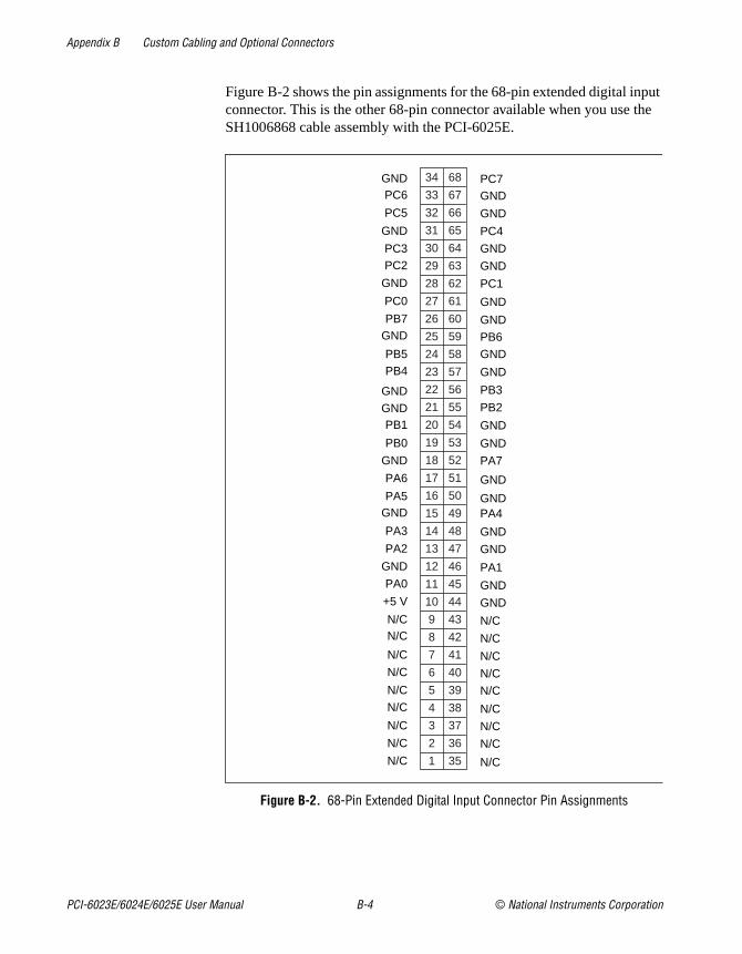
Appendix B Custom Cabling and Optional Connectors
put the
PCI.book Page 4 Wednesday, September 16, 1998 9:09 AM
Figure B-2 shows the pin assignments for the 68-pin extended digital inconnector. This is the other 68-pin connector available when you use SH1006868 cable assembly with the PCI-6025E.
Figure B-2. 68-Pin Extended Digital Input Connector Pin Assignments
N/C
N/C
N/C
N/C
N/C
N/C
N/C
N/CN/C
+5 V
PA0
GND
PA2
PA3
GNDPA5
PA6
GND
PB0
PB1GND
GND
PB4PB5
GNDPB7
PC0
GND
PC2PC3
GND
PC5
PC6GND
N/C
N/C
N/C
N/C
N/C
N/C
N/C
N/C
N/C
GND
GND
PA1
GND
GND
PA4GND
GND
PA7
GND
GND
PB2
PB3
GND
GND
PB6
GND
GND
PC1
GND
GND
PC4
GND
GNDPC7
1 35
2 36
3 37
4 38
5 39
6 40
7 41
8 42
9 43
10 44
11 45
12 46
13 47
14 48
15 49
16 50
17 51
18 52
19 53
20 54
21 55
22 56
23 57
24 58
25 59
26 60
27 61
28 62
29 63
30 64
31 65
32 66
33 67
34 68
PCI-6023E/6024E/6025E User Manual B-4 © National Instruments Corporation
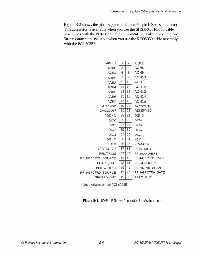
Appendix B Custom Cabling and Optional Connectors
tor. o
bly
PCI.book Page 5 Wednesday, September 16, 1998 9:09 AM
Figure B-3 shows the pin assignments for the 50-pin E Series connecThis connector is available when you use the SH6850 or R6850 cableassemblies with the PCI-6023E and PCI-6024E. It is also one of the tw50-pin connectors available when you use the RI005050 cable assemwith the PCI-6025E.
Figure B-3. 50-Pin E Series Connector Pin Assignments
GPCTR0_OUT
PFI8/GPCTR0_SOURCE
PFI6/WFTRIG
GPCTR1_OUT
PFI3/GPCTR1_SOURCE
PFI1/TRIG2
EXTSTROBE*
+5 VDGND
DIO3
DIO2
DIO1
DIO0
AOGND
DAC1OUT1
AISENSE
ACH7
ACH6
ACH5
ACH4 ACH3
ACH2
ACH1ACH0
AIGND
FREQ_OUT
PFI7/STARTSCAN
PFI5/UPDATE*
PFI2/CONVERT*
PFI0/TRIG1
SCANCLK
+5 V
PFI9/GPCTR0_GATE
PFI4/GPCTR1_GATE
DIO7
DIO6
DIO5
DIO4
DGND
RESERVEDDAC0OUT1
ACH15ACH14ACH13ACH12ACH11ACH10ACH9ACH8AIGND
49 50
47 48
45 46
43 44
41 42
39 40
37 38
35 36
33 34
31 32
29 30
27 28
25 26
23 24
21 22
19 20
17 18
15 16
13 14
11 12
9 10
7 8
5 6
3 4
1 2
1 Not available on the PCI-6023E
© National Instruments Corporation B-5 PCI-6023E/6024E/6025E User Manual

Appendix B Custom Cabling and Optional Connectors
put the
PCI.book Page 6 Wednesday, September 16, 1998 9:09 AM
Figure B-4 shows the pin assignments for the 50-pin extended digital inconnector. This is the other 50-pin connector available when you use R1005050 cable assembly with the PCI-6025E.
Figure B-4. 50-Pin Extended Digital Input Connector Pin Assignments
+5 V
PA0
PA1
PA2
PA3
PA4
PA5
PA6PA7
PB0
PB1
PB2
PB3
PB4
PB5PB6
PB7
PC0
PC1
PC2
PC3
PC4
PC5PC6
PC7
GND
GND
GND
GND
GND
GND
GND
GND
GND
GND
GND
GND
GND
GND
GNDGND
GND
GND
GND
GND
GND
GND
GND
GND
GND
49 50
47 48
45 46
43 44
41 42
39 40
37 38
35 36
33 34
31 32
29 30
27 28
25 26
23 24
21 22
19 20
17 18
15 16
13 14
11 12
9 10
7 8
5 6
3 4
1 2
PCI-6023E/6024E/6025E User Manual B-6 © National Instruments Corporation

© National Instruments Corporation C-1 PCI-6023E/6024E/60
PCI.book Page 1 Wednesday, September 16, 1998 9:09 AM
C
4-bit
f of me less
d ling kS/s
Common Questions
This appendix contains a list of commonly asked questions and their answers relating to usage and special features of your board.
General Information
What is the DAQ-STC?
The DAQ-STC is the System Timing Control application-specific integrated circuit (ASIC) designed by National Instruments and is the backbone of the PCI E Series boards. The DAQ-STC contains seven 2counters and three 16-bit counters. The counters are divided into the following three groups:
• Analog input—two 24-bit, two 16-bit counters
• Analog output—three 24-bit, one 16-bit counters
• General-purpose counter/timer functions—two 24-bit counters
The groups can be configured independently with timing resolutions o50 ns or 10 µs. With the DAQ-STC, you can interconnect a wide varietyinternal timing signals to other internal blocks. The interconnection scheis quite flexible and completely software configurable. New capabilitiessuch as buffered pulse generation, equivalent time sampling, and seamchanging of the sampling rate are possible.
What does sampling rate mean to me?
It means that this is the fastest you can acquire data on your board anstill achieve accurate results. For example, these boards have a samprate of 200 kS/s. This sampling rate is aggregate: one channel at 200or two channels at 100 kS/s per channel illustrates the relationship.
What type of 5 V protection do the boards have?
The boards have 5 V lines equipped with a self-resetting 1 A fuse.
25E User Manual
Appendix C Common Questions
PCI
ced
e de
hes
s
PCI.book Page 2 Wednesday, September 16, 1998 9:09 AM
Installation and ConfigurationHow do I set the base address for a my board?
The base address of your board is assigned automatically through thebus protocol. This assignment is completely transparent to you.
What jumpers should I be aware of when configuring my PCI E Series board?
The PCI E Series boards are jumperless and switchless.
Which National Instruments document should I read first to get started using DAQ software?
Your NI-DAQ or application software release notes documentation is always the best starting place.
Analog Input and OutputI’m using my board in differential analog input mode and I have connected a differential input signal, but my readings are random and drift rapidly. What’s wrong?
Check your ground reference connections. Your signal may be referento a level that is considered floating with reference to the board ground reference. Even if you are in differential mode, the signal must still be referenced to the same ground level as the board reference. There arvarious methods of achieving this while maintaining a high common-morejection ratio (CMRR). These methods are outlined in Chapter 4, Signal Connections.
I’m using the DACs to generate a waveform, but I discovered with a digital oscilloscope that there are glitches on the output signal. Is this normal?
When it switches from one voltage to another, any DAC produces glitcdue to released charges. The largest glitches occur when the most significant bit (MSB) of the D/A code switches. You can build a lowpasdeglitching filter to remove some of these glitches, depending on the frequency and nature of your output signal.
PCI-6023E/6024E/6025E User Manual C-2 © National Instruments Corporation

Appendix C Common Questions
ing eps d
set
e
n he bers ters
PCI.book Page 3 Wednesday, September 16, 1998 9:09 AM
Can I synchronize a one-channel analog input data acquisition with a one-channel analog output waveform generation on my PCI E Series board?
Yes. One way to accomplish this is to use the waveform generation timpulses to control the analog input data acquisition. To do this, follow st1 through 4 below, in addition to the usual steps for data acquisition anwaveform generation configuration.
1. Enable the PFI5 line for output, as follows:
• If you are using NI-DAQ, call Select_Signal(deviceNumber, ND_PFI_5,
ND_OUT_UPDATE, ND_HIGH_TO_LOW).
• If you are using LabVIEW, invoke Route Signal VI with signal name set to PFI5 and signal source set to AO Update.
2. Set up data acquisition timing so that the timing signal for A/D conversion comes from PFI5, as follows:
• If you are using NI-DAQ, call Select_Signal(deviceNumber, ND_IN_CONVERT,
ND_PFI_5, ND_HIGH_TO_LOW).
• If you are using LabVIEW, invoke AI Clock Config VI with clocksource code set to PFI pin, high to low, and clock source stringto 5.
3. Initiate analog input data acquisition, which will start only when thanalog output waveform generation starts.
4. Initiate analog output waveform generation.
Timing and Digital I/OWhat types of triggering can be hardware-implemented on my board?
Digital triggering is hardware-supported on every board.
Will the counter/timer applications that I wrote previously work with the DAQ-STC?
If you are using NI-DAQ with LabVIEW, some of your applications drawusing the CTR VIs will still run. However, there are many differences in tcounters between the PCI E Series and other boards; the counter numare different, timebase selections are different, and the DAQ-STC coun
© National Instruments Corporation C-3 PCI-6023E/6024E/6025E User Manual

Appendix C Common Questions
e ill
R
plus lls.
u Use
tions
se r,
al r
ble
o
igh
PCI.book Page 4 Wednesday, September 16, 1998 9:09 AM
are 24-bit counters (unlike the 16-bit counters on boards without the DAQ-STC).
If you are using the NI-DAQ language interface or LabWindows/CVI, thanswer is no, the counter/timer applications that you wrote previously wnot work with the DAQ-STC. You must use the GPCTR functions; ICTand CTR functions will not work with the DAQ-STC. The GPCTR functions have the same capabilities as the ICTR and CTR functions, more, but you must rewrite the application with the GPCTR function ca
I’m using one of the general-purpose counter/timers on my board, but I do not see the counter/timer output on the I/O connector. What am I doing wrong?
If you are using the NI-DAQ language interface or LabWindows/CVI, yomust configure the output line to output the signal to the I/O connector. the Select_Signal call in NI-DAQ to configure the output line. By default, all timing I/O lines except EXTSTROBE* are tri-stated.
What are the PFIs and how do I configure these lines?
PFIs are Programmable Function Inputs. These lines serve as connecto virtually all internal timing signals.
If you are using the NI-DAQ language interface or LabWindows/CVI, uthe Select_Signal function to route internal signals to the I/O connectoroute external signals to internal timing sources, or tie internal timing signals together.
If you are using NI-DAQ with LabVIEW and you want to connect externsignal sources to the PFI lines, you can use AI Clock Config, AI TriggeConfig, AO Clock Config, AO Trigger and Gate Config, CTR Mode Config, and CTR Pulse Config advanced level VIs to indicate which function the connected signal will serve. Use the Route Signal VI to enathe PFI lines to output internal signals.
Caution If you enable a PFI line for output, do not connect any external signal source tit; if you do, you can damage the board, the computer, and the connected equipment.
What are the power-on states of the PFI and DIO lines on the I/O connector?
At system power-on and reset, both the PFI and DIO lines are set to himpedance by the hardware. This means that the board circuitry is notactively driving the output either high or low. However, these lines
!
PCI-6023E/6024E/6025E User Manual C-4 © National Instruments Corporation

Appendix C Common Questions
n or te
ut
PCI.book Page 5 Wednesday, September 16, 1998 9:09 AM
may have pull-up or pull-down resistors connected to them as shown iTable 4-2. These resistors weakly pull the output to either a logic high logic low state. For example, DIO(0) will be in the high impedance staafter power on, and Table 4-2 shows that there is a 50 kΩ pull-up resistor. This pull-up resistor will set the DIO(0) pin to a logic high when the outpis in a high impedance state.
© National Instruments Corporation C-5 PCI-6023E/6024E/6025E User Manual
© National Instruments Corporation D-1 PCI-6023E/6024E/60
PCI.book Page 1 Wednesday, September 16, 1998 9:09 AM
D
ryand your
quickly P site, try the r staffed
files ownload to use u can
Customer Communication
For your convenience, this appendix contains forms to help you gather the information necessato help us solve your technical problems and a form you can use to comment on the product documentation. When you contact us, we need the information on the Technical Support Formthe configuration form, if your manual contains one, about your system configuration to answerquestions as quickly as possible.
National Instruments has technical assistance through electronic, fax, and telephone systems toprovide the information you need. Our electronic services include a bulletin board service, an FTa fax-on-demand system, and e-mail support. If you have a hardware or software problem, first electronic support systems. If the information available on these systems does not answer youquestions, we offer fax and telephone support through our technical support centers, which areby applications engineers.
Electronic Services
Bulletin Board SupportNational Instruments has BBS and FTP sites dedicated for 24-hour support with a collection ofand documents to answer most common customer questions. From these sites, you can also dthe latest instrument drivers, updates, and example programs. For recorded instructions on howthe bulletin board and FTP services and for BBS automated information, call 512 795 6990. Yoaccess these services at:
United States: 512 794 5422Up to 14,400 baud, 8 data bits, 1 stop bit, no parity
United Kingdom: 01635 551422Up to 9,600 baud, 8 data bits, 1 stop bit, no parity
France: 01 48 65 15 59Up to 9,600 baud, 8 data bits, 1 stop bit, no parity
FTP SupportTo access our FTP site, log on to our Internet host, ftp.natinst.com , as anonymous and use your Internet address, such as [email protected] , as your password. The support files anddocuments are located in the /support directories.
25E User Manual

wide t
l at the we can
al act
PCI.book Page 2 Wednesday, September 16, 1998 9:09 AM
Fax-on-Demand SupportFax-on-Demand is a 24-hour information retrieval system containing a library of documents on arange of technical information. You can access Fax-on-Demand from a touch-tone telephone a512 418 1111.
E-Mail Support (Currently USA Only)You can submit technical support questions to the applications engineering team through e-maiInternet address listed below. Remember to include your name, address, and phone number socontact you with solutions and suggestions.
Telephone and Fax SupportNational Instruments has branch offices all over the world. Use the list below to find the technicsupport number for your country. If there is no National Instruments office in your country, contthe source from which you purchased your software to obtain support.
Country Telephone FaxAustralia 03 9879 5166 03 9879 6277Austria 0662 45 79 90 0 0662 45 79 90 19Belgium 02 757 00 20 02 757 03 11Brazil 011 288 3336 011 288 8528Canada (Ontario) 905 785 0085 905 785 0086Canada (Québec) 514 694 8521 514 694 4399Denmark 45 76 26 00 45 76 26 02Finland 09 725 725 11 09 725 725 55France 01 48 14 24 24 01 48 14 24 14Germany 089 741 31 30 089 714 60 35Hong Kong 2645 3186 2686 8505Israel 03 6120092 03 6120095Italy 02 413091 02 41309215Japan 03 5472 2970 03 5472 2977Korea 02 596 7456 02 596 7455Mexico 5 520 2635 5 520 3282Netherlands 0348 433466 0348 430673Norway 32 84 84 00 32 84 86 00Singapore 2265886 2265887Spain 91 640 0085 91 640 0533Sweden 08 730 49 70 08 730 43 70Switzerland 056 200 51 51 056 200 51 55Taiwan 02 377 1200 02 737 4644United Kingdom 01635 523545 01635 523154United States 512 795 8248 512 794 5678
PCI-6023E/6024E/6025E User Manual D-2 © National Instruments Corporation

nd use orm
,
____
____
____
____
____
____
__
____
___
____
____
____
____
____
____
____
____
____
____
____
____
____
____
____
____
____
PCI.book Page 3 Wednesday, September 16, 1998 9:09 AM
Technical Support FormPhotocopy this form and update it each time you make changes to your software or hardware, athe completed copy of this form as a reference for your current configuration. Completing this faccurately before contacting National Instruments for technical support helps our applications engineers answer your questions more efficiently.
If you are using any National Instruments hardware or software products related to this probleminclude the configuration forms from their user manuals. Include additional pages if necessary.
Name ______________________________________________________________________
Company ___________________________________________________________________
Address ____________________________________________________________________
___________________________________________________________________________
Fax ( ___ ) ________________Phone ( ___ ) ______________________________________
Computer brand____________ Model ___________________Processor _____________________
Operating system (include version number) ________________________________________
Clock speed ______MHz RAM _____MB Display adapter ________________________
Mouse ___yes ___no Other adapters installed___________________________________
Hard disk capacity _____MB Brand______________________________________________
Instruments used _____________________________________________________________
___________________________________________________________________________
National Instruments hardware product model _____________ Revision ____________________
Configuration _______________________________________________________________
National Instruments software product ___________________ Version _____________________
Configuration _______________________________________________________________
The problem is: ______________________________________________________________
___________________________________________________________________________
___________________________________________________________________________
___________________________________________________________________________
___________________________________________________________________________
List any error messages: _______________________________________________________
___________________________________________________________________________
___________________________________________________________________________
The following steps reproduce the problem: _______________________________________
___________________________________________________________________________
___________________________________________________________________________
___________________________________________________________________________
___________________________________________________________________________

item. , and ore your
____
____
____
____
____
____
____
_____
____
____
____
____
____
____
____
____
____
____
____
_____
____
____
PCI.book Page 5 Wednesday, September 16, 1998 9:09 AM
PCI-6023E/6024E/6025E Hardware and Software Configuration FormRecord the settings and revisions of your hardware and software on the line to the right of eachComplete a new copy of this form each time you revise your software or hardware configurationuse this form as a reference for your current configuration. Completing this form accurately befcontacting National Instruments for technical support helps our applications engineers answer questions more efficiently.
National Instruments ProductsHardware revision ___________________________________________________________
Interrupt level of hardware _____________________________________________________
DMA channels of hardware ____________________________________________________
Base I/O address of hardware ___________________________________________________
Programming choice _________________________________________________________
National Instruments software __________________________________________________
Other boards in system ________________________________________________________
Base I/O address of other boards _______________________________________________
DMA channels of other boards _________________________________________________
Interrupt level of other boards __________________________________________________
Other ProductsComputer make and model ____________________________________________________
Microprocessor ______________________________________________________________
Clock frequency or speed ______________________________________________________
Type of video board installed ___________________________________________________
Operating system version ______________________________________________________
Operating system mode _______________________________________________________
Programming language _______________________________________________________
Programming language version _________________________________________________
Other boards in system ________________________________________________________
Base I/O address of other boards _______________________________________________
DMA channels of other boards _________________________________________________
Interrupt level of other boards __________________________________________________

ducts.
____
____
____
____
____
____
____
____
____
____
____
____
____
____
____
____
____
____
____
____
____
PCI.book Page 7 Wednesday, September 16, 1998 9:09 AM
Documentation Comment FormNational Instruments encourages you to comment on the documentation supplied with our proThis information helps us provide quality products to meet your needs.
Title: PCI-6023E/6024E/6025E User Manual
Edition Date: October 1998
Part Number: 322072A-01
Please comment on the completeness, clarity, and organization of the manual.
___________________________________________________________________________
___________________________________________________________________________
___________________________________________________________________________
___________________________________________________________________________
___________________________________________________________________________
___________________________________________________________________________
___________________________________________________________________________
If you find errors in the manual, please record the page numbers and describe the errors.
___________________________________________________________________________
___________________________________________________________________________
___________________________________________________________________________
___________________________________________________________________________
___________________________________________________________________________
___________________________________________________________________________
___________________________________________________________________________
Thank you for your help.
Name _____________________________________________________________________
Title ______________________________________________________________________
Company ___________________________________________________________________
Address ____________________________________________________________________
___________________________________________________________________________
E-Mail Address ______________________________________________________________
Phone ( ___ ) __________________________ Fax ( ___ ) ___________________________
Mail to: Technical Publications Fax to: Technical PublicationsNational Instruments Corporation National Instruments Corporation6504 Bridge Point Parkway 512 794 5678Austin, Texas 78730-5039
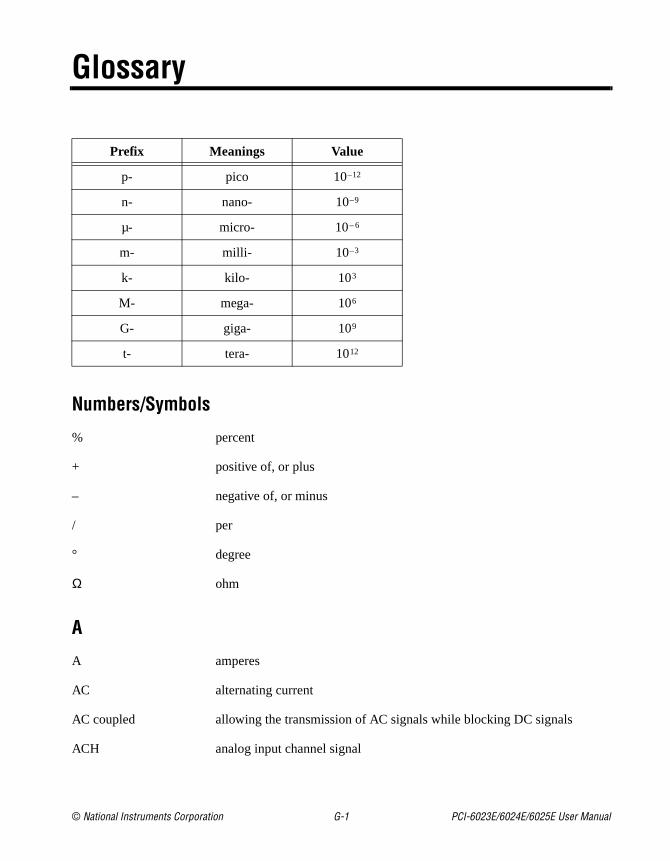
PCI.book Page 1 Wednesday, September 16, 1998 9:09 AM
Glossary
Prefix Meanings Value
p- pico 10–12
n- nano- 10–9
µ- micro- 10– 6
m- milli- 10–3
k- kilo- 103
M- mega- 106
G- giga- 109
t- tera- 1012
Numbers/Symbols
% percent
+ positive of, or plus
– negative of, or minus
/ per
° degree
Ω ohm
A
A amperes
AC alternating current
AC coupled allowing the transmission of AC signals while blocking DC signals
ACH analog input channel signal
© National Instruments Corporation G-1 PCI-6023E/6024E/6025E User Manual
Glossary
its 2-bit
uired
, f a r
ies to
PCI.book Page 2 Wednesday, September 16, 1998 9:09 AM
A/D analog-to-digital
ADC analog-to-digital converter—an electronic device, often an integrated circuit, that converts an analog voltage to a digital number
ADC resolution the resolution of the ADC, which is measured in bits. An ADC with 16 bhas a higher resolution, and thus a higher degree of accuracy, than a 1ADC.
AI analog input
AIGATE analog input gate signal
AIGND analog input ground signal
AISENSE analog input sense signal
alias a false lower frequency component that appears in sampled data acqat too low a sampling rate
amplification a type of signal conditioning that improves accuracy in the resulting digitized signal and reduces noise
ANSI American National Standards Institute
AO analog output
AOGND analog output ground signal
ASIC Application-Specific Integrated Circuit—a proprietary semiconductor component designed and manufactured to perform a set of specific functions for a specific customer
asynchronous (1) hardware—a property of an event that occurs at an arbitrary timewithout synchronization to a reference clock (2) software—a property ofunction that begins an operation and returns prior to the completion otermination of the operation
attenuate to decrease the amplitude of a signal
B
bandwidth the range of frequencies present in a signal, or the range of frequencwhich a measuring device can respond
PCI-6023E/6024E/6025E User Manual G-2 © National Instruments Corporation
Glossary
able ss.
of
urces.
ple,
lowed
ter. are
e
he tial. sist
ling ck.
PCI.book Page 3 Wednesday, September 16, 1998 9:09 AM
base address a memory address that serves as the starting address for programmregisters. All other addresses are located by adding to the base addre
BIOS basic input/output system—BIOS functions are the fundamental level any PC or compatible computer. BIOS functions embody the basic operations needed for successful use of the computer’s hardware reso
bipolar a signal range that includes both positive and negative values (for exam–5 V to +5 V)
breakdown voltage the voltage high enough to cause breakdown of optical isolation, semiconductors, or dielectric materials. See also working voltage.
burst-mode a high-speed data transfer in which the address of the data is sent folby back-to-back data words while a physical signal is asserted
bus the group of conductors that interconnect individual circuitry in a compuTypically, a bus is the expansion vehicle to which I/O or other devices connected. Examples of PC buses are the ISA and PCI bus.
bus master a type of a plug-in board or controller with the ability to read and writdevices on the computer bus
C
C Celsius
CalDAC calibration DAC
CH channel—pin or wire lead to which you apply or from which you read tanalog or digital signal. Analog signals can be single-ended or differenFor digital signals, you group channels to form ports. Ports usually conof either four or eight digital channels.
channel clock the clock controlling the time interval between individual channel sampwithin a scan. Boards with simultaneous sampling do not have this clo
CMRR common-mode rejection ratio—a measure of an instrument’s ability toreject interference from a common-mode signal, usually expressed in decibels (dB)
cold-junction compensation
a method of compensating for inaccuracies in thermocouple circuits
© National Instruments Corporation G-3 PCI-6023E/6024E/6025E User Manual

Glossary
nal
of the
ent a that
nnel
f ns
tput
ut
age
a of nd
PCI.book Page 4 Wednesday, September 16, 1998 9:09 AM
common-mode range the input range over which a circuit can handle a common-mode sig
common-mode signal the mathematical average voltage, relative to the computer’s ground,signals from a differential input
conversion time the time required, in an analog input or output system, from the momchannel is interrogated (such as with a read instruction) to the momentaccurate data is available
CONVERT* convert signal
counter/timer a circuit that counts external pulses or clock pulses (timing)
crosstalk an unwanted signal on one channel due to an input on a different cha
CTR counter
current drive capability the amount of current a digital or analog output channel is capable osourcing or sinking while still operating within voltage range specificatio
current sinking the ability of a DAQ board to dissipate current for analog or digital ousignals
current sourcing the ability of a DAQ board to supply current for analog or digital outpsignals
D
D/A digital-to-analog
DAC digital-to-analog converter—an electronic device, often an integrated circuit, that converts a digital number into a corresponding analog voltor current
DAC0OUT analog channel 0 output signal
DAC1OUT analog channel 1 output signal
DAQ data acquisition—(1) collecting and measuring electrical signals from sensors, transducers, and test probes or fixtures and inputting them tocomputer for processing; (2) collecting and measuring the same kindselectrical signals with A/D and/or DIO boards plugged into a computer, apossibly generating control signals with D/A and/or DIO boards in the same computer
PCI-6023E/6024E/6025E User Manual G-4 © National Instruments Corporation
Glossary
wo
rom
rom
ring
d or
n be
s A/D
PCI.book Page 5 Wednesday, September 16, 1998 9:09 AM
dB decibel—the unit for expressing a logarithmic measure of the ratio of tsignal levels: dB=20log10 V1/V2, for signals in volts
DC direct current
DC coupled allowing the transmission of both AC and DC signals
DGND digital ground signal
DIFF differential mode
differential input an analog input consisting of two terminals, both of which are isolated fcomputer ground, whose difference is measured
digital port See port.
DIN Deutsche Industrie Norme
DIO digital input/output
dithering the addition of Gaussian noise to an analog input signal
DMA direct memory access—a method by which data can be transferred to/fcomputer memory from/to a device or memory on the bus while the processor does something else. DMA is the fastest method of transferdata to/from computer memory.
DNL differential nonlinearity—a measure in least significant bit of the worst-case deviation of code widths from their ideal value of 1 LSB
DO digital output
drivers software that controls a specific hardware device such as a DAQ boara GPIB interface board
E
EEPROM electrically erasable programmable read-only memory—ROM that caerased with an electrical signal and reprogrammed
electrostatically coupled propagating a signal by means of a varying electric field
external trigger a voltage pulse from an external source that triggers an event such aconversion
© National Instruments Corporation G-5 PCI-6023E/6024E/6025E User Manual

Glossary
t to re r ntil the r.
time,
on the ted
m
olute .
ibels
PCI.book Page 6 Wednesday, September 16, 1998 9:09 AM
EXTSTROBE external strobe signal
F
FIFO first-in first-out memory buffer—the first data stored is the first data senthe acceptor. FIFOs are often used on DAQ devices to temporarily stoincoming or outgoing data until that data can be retrieved or output. Foexample, an analog input FIFO stores the results of A/D conversions uthe data can be retrieved into system memory, a process that requiresservicing of interrupts and often the programming of the DMA controlleThis process can take several milliseconds in some cases. During this data accumulates in the FIFO for future retrieval. With a larger FIFO, longer latencies can be tolerated. In the case of analog output, a FIFOpermits faster update rates, because the waveform data can be stored FIFO ahead of time. This again reduces the effect of latencies associawith getting the data from system memory to the DAQ device.
filtering a type of signal conditioning that allows you to filter unwanted signals frothe signal you are trying to measure
floating signal sources signal sources with voltage signals that are not connected to an absreference or system ground. Also called nonreferenced signal sourcesSome common example of floating signal sources are batteries, transformers, or thermocouples.
FREQ_OUT frequency output signal
ft feet
G
gain the factor by which a signal is amplified, sometimes expressed in dec
gain accuracy a measure of deviation of the gain of an amplifier from the ideal gain
GATE gate signal
glitch an unwanted momentary deviation from a desired signal
GPCTR general purpose counter
GPCTR0_GATE general purpose counter 0 gate signal
PCI-6023E/6024E/6025E User Manual G-6 © National Instruments Corporation

Glossary
bus
8,
3 dB
cepts ched
m
PCI.book Page 7 Wednesday, September 16, 1998 9:09 AM
GPCTR0_OUT general purpose counter 0 output signal
GPCTR0_SOURCE general purpose counter 0 clock source signal
GPCTR0_UP_DOWN general purpose counter 0 up down
GPCTR1_GATE general purpose counter 1 gate signal
GPCTR1_OUT general purpose counter 1 output signal
GPCTR1_SOURCE general purpose counter 1 clock source signal
GPCTR1_UP_DOWN general purpose counter 1 up down
GPIB General Purpose Interface bus, synonymous with HP-IB. The standardused for controlling electronic instruments with a computer. Also calledIEEE 488 bus because it is defined by ANSI/IEEE Standards 488-197488.1-1987, and 488.2-1987.
grounded measurement system
See referenced single-ended measurement system.
H
h hour
half-power bandwidth the frequency range over which a circuit maintains a level of at least –with respect to the maximum level
handshaked digital I/O a type of digital acquisition/generation where a device or module acor transfers data after a digital pulse has been received. Also called latdigital I/O.
hex hexadecimal
Hz hertz—the number of events per second
I
in. inches
INL integral nonlinearity—a measure in LSB of the worst-case deviation frothe ideal A/D or D/A transfer characteristic of the analog I/O circuitry
© National Instruments Corporation G-7 PCI-6023E/6024E/6025E User Manual

Glossary
uit
XI,
on
the
task
there
PCI.book Page 8 Wednesday, September 16, 1998 9:09 AM
input bias current the current that flows into the inputs of a circuit
input impedance the resistance and capacitance between the input terminals of a circ
input offset current the difference in the input bias currents of the two inputs of an instrumentation amplifier
instrument driver a set of high-level software functions that controls a specific GPIB, Vor RS-232 programmable instrument or a specific plug-in DAQ board. Instrument drivers are available in several forms, ranging from a functicallable language to a virtual instrument (VI) in LabVIEW.
instrumentation amplifier
a circuit whose output voltage with respect to ground is proportional to difference between the voltages at its two high impedance inputs
interrupt a computer signal indicating that the CPU should suspend its current to service a designated activity
interrupt level the relative priority at which a device can interrupt
interval scanning scanning method where there is a longer interval between scans thanis between individual channels comprising a scan
I/O input/output—the transfer of data to/from a computer system involvingcommunications channels, operator interface devices, and/or data acquisition and control interfaces
IOH current, output high
IOL current, output low
IRQ interrupt request
K
k kilo—the standard metric prefix for 1,000, or 103, used with units of measure such as volts, hertz, and meters
K kilo—the prefix for 1,024, or 210, used with B in quantifying data or computer memory
kS 1,000 samples
PCI-6023E/6024E/6025E User Manual G-8 © National Instruments Corporation
Glossary
ore hese nly hile
bus
r to
PCI.book Page 9 Wednesday, September 16, 1998 9:09 AM
L
LabVIEW laboratory virtual instrument engineering workbench
LED light-emitting diode
library a file containing compiled object modules, each comprised of one of mfunctions, that can be linked to other object modules that make use of tfunctions. NIDAQMSC.LIB is a library that contains NI-DAQ functions.The NI-DAQ function set is broken down into object modules so that othe object modules that are relevant to your application are linked in, wthose object modules that are not relevant are not linked.
linearity the adherence of device response to the equation R = KS, where R = response, S = stimulus, and K = a constant
LSB least significant bit
M
MIO multifunction I/O
MITE MXI Interface to Everything—a custom ASIC designed by National Instruments that implements the PCI bus interface. The MITE supportsmastering for high-speed data transfers over the PCI bus.
MS million samples
MSB most significant bit
mux multiplexer—a switching device with multiple inputs that sequentially connects each of its inputs to its output, typically at high speeds, in ordemeasure several signals with a single analog input channel
N
NC normally closed, or not connected
NI-DAQ National Instruments driver software for DAQ hardware
© National Instruments Corporation G-9 PCI-6023E/6024E/6025E User Manual

Glossary
such hts, dio
and
gital ne.
ute
stem
us
final
to
bus tions;
nd
PCI.book Page 10 Wednesday, September 16, 1998 9:09 AM
noise an undesirable electrical signal—Noise comes from external sources as the AC power line, motors, generators, transformers, fluorescent ligsoldering irons, CRT displays, computers, electrical storms, welders, ratransmitters, and internal sources such as semiconductors, resistors, capacitors. Noise corrupts signals you are trying to send or receive.
nonlatched digital I/O a type of digital acquisition/generation where LabVIEW updates the dilines or port states immediately or returns the digital value of an input liAlso called immediate digital I/O or non-handshaking.
nonreferenced signal sources
signal sources with voltage signals that are not connected to an absolreference or system ground. Also called floating signal sources. Somecommon example of nonreferenced signal sources are batteries, transformers, or thermocouples.
NRSE nonreferenced single-ended mode—all measurements are made withrespect to a common (NRSE) measurement system reference, but thevoltage at this reference can vary with respect to the measurement syground
O
OUT output pin—a counter output pin where the counter can generate varioTTL pulse waveforms
output settling time the amount of time required for the analog output voltage to reach itsvalue within specified limits
output slew rate the maximum rate of change of analog output voltage from one levelanother
P
PCI Peripheral Component Interconnect—a high-performance expansion architecture originally developed by Intel to replace ISA and EISA. It isachieving widespread acceptance as a standard for PCs and work-stait offers a theoretical maximum transfer rate of 132 Mbytes/s.
peak to peak a measure of signal amplitude; the difference between the highest alowest excursions of the signal
PFI programmable function input
PCI-6023E/6024E/6025E User Manual G-10 © National Instruments Corporation

Glossary
ources
r
r of
with the
PCI.book Page 11 Wednesday, September 16, 1998 9:09 AM
PFI0/TRIG1 PFI0/trigger 1
PFI1/TRIG2 PFI1/trigger 2
PFI2/CONVERT* PFI2/convert
PFI3/GPCTR1_SOURCE
PFI3/general purpose counter 1 source
PFI4/GPCTR1_GATE PFI4/general purpose counter 1 gate
PFI5/UPDATE* PFI5/update
PFI6/WFTRIG PFI6/waveform trigger
PFI7/STARTSCAN PFI7/start of scan
PFI8/GPCTR0_SOURCE
PFI8/general purpose counter 0 source
PFI9/GPCTR0_GATE PFI9/general purpose counter 0 gate
PGIA programmable gain instrumentation amplifier
Plug and Play devices devices that do not require DIP switches or jumpers to configure reson the devices—also called switchless devices
port (1) a communications connection on a computer or a remote controlle(2) a digital port, consisting of four or eight lines of digital input and/or output
posttriggering the technique used on a DAQ board to acquire a programmed numbesamples after trigger conditions are met
PPI programmable peripheral interface
ppm parts per million
pretriggering the technique used on a DAQ board to keep a continuous buffer filleddata, so that when the trigger conditions are met, the sample includesdata leading up to the trigger condition
pts points
pu pullup
© National Instruments Corporation G-11 PCI-6023E/6024E/6025E User Manual
Glossary
en a
uired
und, rces.
arity e
t nt of 96
step
of the
pect a
PCI.book Page 12 Wednesday, September 16, 1998 9:09 AM
pulse trains multiple pulses
pulsed output a form of counter signal generation by which a pulse is outputted whcounter reaches a certain value
Q
quantization error the inherent uncertainty in digitizing an analog value due to the finiteresolution of the conversion process
R
RAM random-access memory
real time a property of an event or system in which data is processed as it is acqinstead of being accumulated and processed at a later time
referenced signal sources
signal sources with voltage signals that are referenced to a system grosuch as the earth or a building ground. Also called grounded signal sou
relative accuracy a measure in LSB of the accuracy of an ADC. It includes all non-lineand quantization errors. It does not include offset and gain errors of thcircuitry feeding the ADC.
resolution the smallest signal increment that can be detected by a measuremensystem. Resolution can be expressed in bits, in proportions, or in percefull scale. For example, a system has 12-bit resolution, one part in 4,0resolution, and 0.0244% of full scale.
ribbon cable a flat cable in which the conductors are side by side
rise time the difference in time between the 10% and 90% points of a system’sresponse
rms root mean square—the square root of the average value of the squareinstantaneous signal amplitude; a measure of signal amplitude
RSE referenced single-ended mode—all measurements are made with resto a common reference measurement system or a ground. Also calledgrounded measurement system.
PCI-6023E/6024E/6025E User Manual G-12 © National Instruments Corporation

Glossary
that rds,
the cans.
put . For uires
means
Q
red
rence by
sure, al
PCI.book Page 13 Wednesday, September 16, 1998 9:09 AM
RTSI bus real-time system integration bus—the National Instruments timing busconnects DAQ boards directly, by means of connectors on top of the boafor precise synchronization of functions
S
s seconds
S samples
sample counter the clock that counts the output of the channel clock, in other words,number of samples taken. On boards with simultaneous sampling, thiscounter counts the output of the scan clock and hence the number of s
scan one or more analog or digital input samples. Typically, the number of insamples in a scan is equal to the number of channels in the input groupexample, one pulse from the scan clock produces one scan which acqone new sample from every analog input channel in the group.
scan clock the clock controlling the time interval between scans.
scan rate the number of scans per second. For example, a scan rate of 10 Hz sampling each channel 10 times per second.
SCXI Signal Conditioning eXtensions for Instrumentation—the National Instruments product line for conditioning low-level signals within an external chassis near sensors so only high-level signals are sent to DAboards in the noisy PC environment
SE single-ended—a term used to describe an analog input that is measuwith respect to a common ground
self-calibrating a property of a DAQ board that has an extremely stable onboard refeand calibrates its own A/D and D/A circuits without manual adjustmentsthe user
sensor a device that responds to a physical stimulus (heat, light, sound, presmotion, flow, and so on), and produces a corresponding electrical sign
settling time the amount of time required for a voltage to reach its final value withinspecified limits
© National Instruments Corporation G-13 PCI-6023E/6024E/6025E User Manual
Glossary
cy t
on a
s
r
urces
nce nd
when
PCI.book Page 14 Wednesday, September 16, 1998 9:09 AM
Shannon Sampling Theorem
a law of sampling theory stating that if a continuous bandwidth-limitedsignal contains no frequency components higher than half the frequenat which it is sampled, then the original signal can be recovered withoudistortion
S/H sample-and-hold—a circuit that acquires and stores an analog voltagecapacitor for a short period of time
signal conditioning the manipulation of signals to prepare them for digitizing
SISOURCE SI counter clock signal
SNR signal-to-noise ratio—the ratio of the overall rms signal level to the rmnoise level, expressed in decibels
software trigger a programmed event that triggers an event such as data acquisition
software triggering a method of triggering in which you simulate an analog trigger using software. Also called conditional retrieval.
SOURCE source signal
SS simultaneous sampling—a property of a system in which each input ooutput channel is digitized or updated at the same instant
S/s samples per second—used to express the rate at which a DAQ boardsamples an analog signal
STARTSCAN start scan signal
STC system timing controller
switchless device devices that do not require dip switches or jumpers to configure resoon the devices—also called Plug and Play devices
synchronous (1) hardware—a property of an event that is synchronized to a refereclock (2) software—a property of a function that begins an operation areturns only when the operation is complete
system noise a measure of the amount of noise seen by an analog circuit or an ADCthe analog inputs are grounded
PCI-6023E/6024E/6025E User Manual G-14 © National Instruments Corporation

Glossary
alue
nic
l to
ulated
um
l to om every
PCI.book Page 15 Wednesday, September 16, 1998 9:09 AM
T
TC terminal count—the highest value of a counter
T/H track-and-hold—a circuit that tracks an analog voltage and holds the von command
THD total harmonic distortion—the ratio of the total rms signal due to harmodistortion to the overall rms signal, in decibel or a percentage
THD+N signal-to-THD plus noise—the ratio in decibels of the overall rms signathe rms signal of harmonic distortion plus noise introduced
throughput rate the data, measured in bytes/s, for a given continuous operation, calcto include software overhead.
transducer See sensor
transfer rate the rate, measured in bytes/s, at which data is moved from source todestination after software initialization and set up operations; the maximrate at which the hardware can operate
TRIG trigger signal
trigger any event that causes or starts some form of data capture
TTL transistor-transistor logic
U
UI update interval
unipolar a signal range that is always positive (for example, 0 to +10 V)
UISOURCE update interval counter clock signal
update the output equivalent of a scan. One or more analog or digital output samples. Typically, the number of output samples in an update is equathe number of channels in the output group. For example, one pulse frthe update clock produces one update which sends one new sample toanalog output channel in the group.
update rate the number of output updates per second
© National Instruments Corporation G-15 PCI-6023E/6024E/6025E User Manual

Glossary
ic
,
PCI.book Page 16 Wednesday, September 16, 1998 9:09 AM
V
V volts
VDC volts direct current
VI virtual instrument—(1) a combination of hardware and/or software elements, typically used with a PC, that has the functionality of a classstand-alone instrument (2) a LabVIEW software module (VI), which consists of a front panel user interface and a block diagram program
VIH volts, input high
VIL volts, input low
Vin volts in
Vm measured voltage
VOH volts, output high
VOL volts, output low
Vref reference voltage
Vrms volts, root mean square
W
waveform multiple voltage readings taken at a specific sampling rate
WFTRIG waveform generation trigger signal
working voltage the highest voltage that should be applied to a product in normal usenormally well under the breakdown voltage for safety margin. See alsobreakdown voltage.
PCI-6023E/6024E/6025E User Manual G-16 © National Instruments Corporation
PCI.book Page 1 Wednesday, September 16, 1998 9:09 AM
Index
4
Numbers+5 V signal
analog I/O pin assignments (table), 4-4description (table), 4-4self-resetting fuse, C-1
82C55A Programmable Peripheral Interface, 3-6
AACH<0..15> signal
description (table), 4-4signal summary (table), 4-7
ACK* signaldescription (table), 4-26mode 1 output timing (figure), 4-28mode 2 bidirectional timing (figure), 4-29
acquisition timing connections. See DAQ timing connections.
AIGATE signal, 4-39AIGND signal
analog input mode, 4-10description (table), 4-4signal summary (table), 4-7
AISENSE signaldescription (table), 4-4NRSE mode, 4-10signal summary (table), 4-6
analog inputcommon questions, C-2 to C-3dither, 3-3 to 3-4input range, 3-2 to 3-3multichannel scanning considerations, 3-4
to 3-5types of signal sources, 4-8 to 4-9
floating signal sources, 4-9ground-referenced signal sources, 4-9
analog input modes, 4-8 to 4-19
available input configurations (table), 3-2common-mode signal rejection
considerations, 4-19differential connections, 4-13 to 4-16
ground-referenced signal sources, 4-1nonreferenced or floating signal
sources, 4-15 to 4-16exceeding common-mode input ranges
(caution), 4-10overview, 3-2PGIA (figure), 4-10recommended input connections
(figure), 4-12single-ended connection, 4-17 to 4-18
floating signal sources (RSE configuration), 4-18
grounded signal sources (NRSE configuration), 4-18 to 4-19
summary of input connections (table), 4-12analog input specifications, A-1 to A-4
accuracy information, A-2amplifier characteristics, A-3dynamic characteristics, A-4input characteristics, A-1 to A-2stability, A-4transfer characteristics, A-3
analog outputanalog output glitch, 3-5common questions, C-2 to C-3overview, 3-5signal connections, 4-20
analog output specifications, A-4 to A-6accuracy information, A-5dynamic characteristics, A-6output characteristics, A-4 to A-5stability, A-6transfer characteristics, A-5voltage output, A-6
© National Instruments Corporation I-1 PCI-6023E/6024E/6025E User Manual

Index
PCI.book Page 2 Wednesday, September 16, 1998 9:09 AM
AOGND signaldescription (table), 4-4signal summary (table), 4-7
Bbipolar input, 3-2block diagram, 3-1bulletin board support, D-1
Ccables. See also I/O connectors.
custom cabling, B-1 to B-2field wiring considerations, 4-49 to 4-50optional equipment, 1-6
calibration, 5-1 to 5-3adjusting gain error, 5-3external calibration, 5-2 to 5-3loading calibration constants, 5-1 to 5-2self-calibration, 5-2specifications, A-9
charge injection, 3-5clocks, board and RTSI, 3-8common-mode signal rejection
considerations, 4-19commonly asked questions. See questions and
answers.ComponentWorks software, 1-3configuration
common questions, C-2hardware configuration, 2-1 to 2-2
connectors. See I/O connectors.CONVERT* signal
DAQ timing connections, 4-38 to 4-39signal routing (figure), 3-7
custom cabling, B-1 to B-2customer communication, xiv, D-1 to D-2
DDAC0OUT signal
analog output signal connections, 4-20description (table), 4-4signal summary (table), 4-7
DAC1OUT signalanalog output signal connections, 4-20description (table), 4-4signal summary (table), 4-7
DAQ-STC, C-1DAQ timing connections, 4-32 to 4-40
AIGATE signal, 4-39CONVERT* signal, 4-38 to 4-39EXTSTROBE* signal, 4-33 to 4-34SCANCLK signal, 4-33SISOURCE signal, 4-40STARTSCAN signal, 4-36 to 4-38TRIG1 signal, 4-34 to 4-35TRIG2 signal, 4-35 to 4-36typical posttriggered acquisition
(figure), 4-32typical pretriggered acquisition
(figure), 4-33DATA signal
description (table), 4-26mode 1 input timing (figure), 4-27mode 1 output timing (figure), 4-28mode 2 bidirectional timing (figure), 4-29
DGND signaldescription (table), 4-4signal summary (table), 4-7
DIFF modedescription (table), 3-2recommended configuration (figure),
4-12differential connections, 4-13 to 4-16
ground-referenced signal sources, 4-14nonreferenced or floating signal
sources, 4-15 to 4-16when to use, 4-13
PCI-6023E/6024E/6025E User Manual I-2 © National Instruments Corporation

Index
PCI.book Page 3 Wednesday, September 16, 1998 9:09 AM
digital I/O82C55A Programmable Peripheral
Interface for PCI-6025E, 3-6changing DIO power-up state to pulled
low, 4-24 to 4-25common questions, C-3 to C-5overview, 3-6signal connections, 4-21 to 4-23
digital I/O specifications, A-6 to A-8DIO<0..7>, A-7PA<0..7>, PB<0..7>, PC<0..7>,
A-7 to A-8digital trigger specifications, A-8 to A-9DIO<0..7> signal
description (table), 4-4digital I/O signal connections, 4-21digital I/O specifications, A-7signal summary (table), 4-7
dither, 3-3 to 3-4documentation
conventions used in manual, xii-xiiiNational Instruments documentation, xiiiorganization of manual, xi-xiirelated documentation, xiv
Ee-mail support, D-2EEPROM storage of calibration constants, 5-1electronic support services, D-1 to D-2environmental noise, 4-49 to 4-50equipment, optional, 1-6EXTSTROBE* signal
DAQ timing connections, 4-33 to 4-34description (table), 4-5signal summary (table), 4-7
Ffax and telephone support numbers, D-2Fax-on-Demand support, D-2
field wiring considerations, 4-49 to 4-50floating signal sources
description, 4-9differential connections, 4-15 to 4-16single-ended connections (RSE
configuration), 4-18FREQ_OUT signal
description (table), 4-6general-purpose timing signal
connections, 4-49signal summary (table), 4-8
frequently asked questions. See questions and answers.
FTP support, D-1fuse, self-resetting, C-1
Ggain error, adjusting, 5-3general-purpose timing signal connections,
4-43 to 4-49FREQ_OUT signal, 4-49GPCTR0_GATE signal, 4-44 to 4-45GPCTR0_OUT signal, 4-45GPCTR0_SOURCE signal, 4-43 to 4-44GPCTR0_UP_DOWN signal, 4-45GPCTR1_GATE signal, 4-46 to 4-47GPCTR1_OUT signal, 4-47GPCTR1_UP_DOWN signal,
4-47 to 4-49glitch, analog output, 3-5GPCTR0_GATE signal, 4-44 to 4-45GPCTR0_OUT signal
description (table), 4-6general-purpose timing signal
connections, 4-45signal summary (table), 4-8
GPCTR0_SOURCE signal, 4-43 to 4-44GPCTR0_UP_DOWN signal, 4-45GPCTR1_GATE signal, 4-46 to 4-47GPCTR1_OUT signal
© National Instruments Corporation I-3 PCI-6023E/6024E/6025E User Manual
Index
PCI.book Page 4 Wednesday, September 16, 1998 9:09 AM
description (table), 4-5general-purpose timing signal
connections, 4-47signal summary (table), 4-8
GPCTR1_UP_DOWN signal, 4-47 to 4-49ground-referenced signal sources
description, 4-9differential connections, 4-14single-ended connections
(NRSE configuration), 4-18 to 4-19
Hhardware
configuration, 2-1 to 2-2installation, 2-2
hardware overviewanalog input, 3-2 to 3-5
dither, 3-3 to 3-4input mode, 3-2input range, 3-2 to 3-3
analog output, 3-5block diagram, 3-1digital I/O, 3-6timing signal routing, 3-6 to 3-9
board and RTSI clocks, 3-8programmable function inputs,
3-7 to 3-8RTSI triggers, 3-8 to 3-9
II/O connectors, 4-1 to 4-8
exceeding maximum ratings (warning), 4-1
optional connectors, B-2 to B-650-pin E Series connector pin
assignments (figure), B-550-pin extended digital input
connector pin assignments (figure), B-6
68-pin E Series connector pin assignments (figure), B-3
68-pin extended digital input connector pin assignments (figure), B-4
pin assignments (table)PCI-6023E/6024E, 4-2PCI-6025E, 4-3
IBF signaldescription (table), 4-25mode 1 input timing (figure), 4-27mode 2 bidirectional timing (figure), 4-29
input mode. See analog input modes.input range, 3-2 to 3-3
exceeding common-mode input ranges (caution), 4-10
measurement precision (table), 3-3installation
common questions, C-2hardware, 2-2software, 2-1unpacking PCI-6023E/6024E/6025E, 1-2
INTR signaldescription (table), 4-26mode 1 input timing (figure), 4-27mode 1 output timing (figure), 4-28mode 2 bidirectional timing (figure), 4-29
LLabVIEW and LabWindows/CVI application
software, 1-3
Mmanual. See documentation.mode 1 input timing (figure), 4-27mode 1 output timing (figure), 4-28mode 2 bidirectional timing (figure), 4-29multichannel scanning considerations,
3-4 to 3-5
PCI-6023E/6024E/6025E User Manual I-4 © National Instruments Corporation

Index
5
PCI.book Page 5 Wednesday, September 16, 1998 9:09 AM
NNI-DAQ driver software, 1-3 to 1-4noise, environmental, 4-49 to 4-50NRSE (nonreferenced single-ended) mode
configuration, 4-10description (table), 3-2differential connections, 4-15 to 4-16recommended configuration
(figure), 4-12single-ended connections for
ground-referenced signal sources, 4-18 to 4-19
OOBF* signal
description (table), 4-26mode 1 output timing (figure), 4-28mode 2 bidirectional timing (figure), 4-29
operating environment specifications, A-9optional equipment, 1-6
PPA<0..7> signal
description (table), 4-4digital I/O specifications, A-7 to A-8signal summary (table), 4-7
PB<0..7> signaldescription (table), 4-4digital I/O specifications, A-7 to A-8signal summary (table), 4-7
PC<0..7> signaldescription (table), 4-4digital I/O specifications, A-7 to A-8signal summary (table), 4-7
PCI-6023E/6024E/6025E. See also hardware overview.
block diagram, 3-1features, 1-1optional equipment, 1-6
requirements for getting started, 1-2software programming choices, 1-3 to 1-
ComponentWorks, 1-3LabVIEW and
LabWindows/CVI, 1-3National Instruments application
software, 1-3NI-DAQ driver software, 1-3 to 1-4register-level programming, 1-5VirtualBench, 1-3
unpacking, 1-2PFI0/TRIG1 signal
description (table), 4-5signal summary (table), 4-7
PFI1/TRIG2 signaldescription (table), 4-5signal summary (table), 4-7
PFI2/CONVERT* signaldescription (table), 4-5signal summary (table), 4-7
PFI3/GPCTR1_SOURCE signaldescription (table), 4-5signal summary (table), 4-8
PFI4/GPCTR1_GATE signaldescription (table), 4-5signal summary (table), 4-8
PFI5/UPDATE signaldescription (table), 4-6signal summary (table), 4-8
PFI6/WFTRIG signaldescription (table), 4-6signal summary (table), 4-8
PFI7/STARTSCAN signaldescription (table), 4-6signal summary (table), 4-8
PFI8/GPCTR0_SOURCE signaldescription (table), 4-6signal summary (table), 4-8
PFI9/GPCTR0_GATE signaldescription (table), 4-6signal summary (table), 4-8
© National Instruments Corporation I-5 PCI-6023E/6024E/6025E User Manual

Index
PCI.book Page 6 Wednesday, September 16, 1998 9:09 AM
PFIs (programmable function inputs)common questions, C-4 to C-5signal routing, 3-7 to 3-8timing connections, 4-31 to 4-32
PGIA (programmable gain instrumentation amplifier)
analog input modes, 4-10 to 4-11differential connections
ground-referenced signal sources (figure), 4-14
nonreferenced or floating signal sources, 4-15 to 4-16
single-ended connectionsfloating signal sources (figure), 4-18ground-referenced signal sources
(figure), 4-19physical specifications, A-9pin assignments
PCI-6023E/6024E (figure), 4-2PCI-6025E (figure), 4-3
Port C pin assignmentsdescription, 4-23signal assignments (table), 4-23
posttriggered acquisition (figure), 4-32power connections, 4-30power requirement specifications, A-9power-up state, digital I/O, 4-24 to 4-25pretriggered acquisition (figure), 4-33programmable function inputs (PFIs). See
PFIs (programmable function inputs).programmable gain instrumentation amplifier.
See PGIA (programmable gain instrumentation amplifier).
Qquestions and answers, C-1 to C-5
analog input and output, C-2 to C-3general information, C-1installation and configuration, C-2timing and digital I/O, C-3 to C-5
RRD* signal
description (table), 4-26mode 1 input timing (figure), 4-27mode 2 bidirectional timing (figure), 4-29
referenced single-ended input (RSE). See RSE (referenced single-ended) mode.
register-level programming, 1-5requirements for getting started, 1-2RSE (referenced single-ended) mode
configuration, 4-10description (table), 3-2recommended configuration
(figure), 4-12single-ended connections for floating
signal sources, 4-18RTSI bus signal connection (figure), 3-9RTSI clocks, 3-9RTSI trigger lines
overview, 3-8signal connection (figure), 3-9specifications, A-9
Ssampling rate, C-1SCANCLK signal
DAQ timing connections, 4-33description (table), 4-5signal summary (table), 4-7
scanning, multichannel, 3-4 to 3-5settling time, in multichannel scanning, 3-5signal connections
analog input, 4-8 to 4-19common-mode signal rejection
considerations, 4-19differential connection
considerations, 4-13 to 4-16input modes, 4-9 to 4-11single-ended connection
considerations, 4-17 to 4-18
PCI-6023E/6024E/6025E User Manual I-6 © National Instruments Corporation

Index
PCI.book Page 7 Wednesday, September 16, 1998 9:09 AM
summary of input connections (table), 4-12
types of signal sources, 4-8 to 4-9analog output, 4-20digital I/O, 4-21 to 4-23
all boards, 4-21 to 4-22PCI-6025E only, 4-22 to 4-23power-up state, 4-24 to 4-25
field wiring considerations, 4-49 to 4-50I/O connectors, 4-1 to 4-8
exceeding maximum ratings (caution), 4-1
I/O connector signal descriptions (table), 4-4 to 4-6
I/O signal summary (table), 4-7 to 4-8
pin assignments (figure), 4-2 to 4-3I/O connectors, optional, B-2 to B-6
50-pin E Series connector pin assignments (figure), B-5
50-pin extended digital input connector pin assignments (figure), B-6
68-pin E Series connector pin assignments (figure), B-3
68-pin extended digital input connector pin assignments (figure), B-4
Port C pin assignments, 4-23power connections, 4-30timing connections, 4-30 to 4-49
DAQ timing connections, 4-32 to 4-40
general-purpose timing signal connections, 4-43 to 4-49
programmable function input connections, 4-31 to 4-32
waveform generation timing connections, 4-40 to 4-43
timing specifications, 4-25 to 4-29mode 1 input timing (figure), 4-27mode 1 output timing (figure), 4-28
mode 2 bidirectional timing (figure), 4-29
signal names used in diagrams (table), 4-25 to 4-26
signal sources, 4-8 to 4-9floating signal sources, 4-9ground-referenced signal sources, 4-9
single-ended connections, 4-17 to 4-19floating signal sources
(RSE configuration), 4-18grounded signal sources
(NRSE configuration), 4-18 to 4-19when to use, 4-17
SISOURCE signal, 4-40software installation, 2-1software programming choices, 1-3 to 1-5
ComponentWorks, 1-3LabVIEW and LabWindows/CVI, 1-3National Instruments application
software, 1-3NI-DAQ driver software, 1-3 to 1-4register-level programming, 1-5VirtualBench, 1-3
specificationsanalog input, A-1 to A-4
accuracy information, A-2amplifier characteristics, A-3dynamic characteristics, A-4input characteristics, A-1 to A-2stability, A-4transfer characteristics, A-3
analog output, A-4 to A-6accuracy information, A-5dynamic characteristics, A-6output characteristics, A-4 to A-5stability, A-6transfer characteristics, A-5voltage output, A-6
calibration, A-9digital I/O, A-6 to A-8
DIO<0..7>, A-7
© National Instruments Corporation I-7 PCI-6023E/6024E/6025E User Manual

Index
,
PCI.book Page 8 Wednesday, September 16, 1998 9:09 AM
PA<0..7>, PB<0..7>, PC<0..7>,A-7 to A-8
operating environment, A-9physical, A-9power requirement, A-9storage environment, A-9timing I/O, A-8triggers, A-8 to A-9
digital trigger, A-8 to A-9RTSI trigger, A-9
STARTSCAN signal, 4-36 to 4-38STB* signal
description (table), 4-25mode 1 input timing (figure), 4-27mode 2 bidirectional timing (figure), 4-29
storage environment specifications, A-9
Ttechnical support, D-1 to D-2telephone and fax support numbers, D-2timing connections, 4-30 to 4-49
DAQ timing connections, 4-32 to 4-40AIGATE signal, 4-39CONVERT* signal, 4-38 to 4-39EXTSTROBE* signal, 4-33 to 4-34SCANCLK signal, 4-33SISOURCE signal, 4-40STARTSCAN signal, 4-36 to 4-38TRIG1 signal, 4-34 to 4-35TRIG2 signal, 4-35 to 4-36typical posttriggered acquisition
(figure), 4-32typical pretriggered acquisition
(figure), 4-33general-purpose timing signal
connections, 4-43 to 4-49FREQ_OUT signal, 4-49GPCTR0_GATE signal, 4-44 to 4-45GPCTR0_OUT signal, 4-45
GPCTR0_SOURCE signal, 4-43 to 4-44
GPCTR0_UP_DOWN signal, 4-45GPCTR1_GATE signal, 4-46 to 4-47GPCTR1_OUT signal, 4-47GPCTR1_UP_DOWN signal,
4-47 to 4-49overview, 4-30programmable function input
connections, 4-31 to 4-32timing I/O connections (figure), 4-31waveform generation timing connections
4-40 to 4-43UISOURCE signal, 4-42 to 4-43UPDATE* signal, 4-41 to 4-42WFTRIG signal, 4-40 to 4-41
timing I/Ocommon questions, C-3 to C-5specifications, A-8
timing signal routing, 3-6 to 3-9board and RTSI clocks, 3-8CONVERT* signal routing (figure), 3-7programmable function inputs, 3-7 to 3-8RTSI triggers, 3-8 to 3-9
timing specifications, 4-25 to 4-29mode 1 input timing (figure), 4-27mode 1 output timing (figure), 4-28mode 2 bidirectional timing (figure), 4-29signal names used in diagrams
(table), 4-25 to 4-26TRIG1 signal, 4-34 to 4-35TRIG2 signal, 4-35 to 4-36trigger specifications, A-8 to A-9
digital trigger, A-8 to A-9RTSI trigger, A-9
UUISOURCE signal, 4-42 to 4-43unpacking PCI-6023E/6024E/6025E, 1-2UPDATE* signal, 4-41 to 4-42
PCI-6023E/6024E/6025E User Manual I-8 © National Instruments Corporation

Index
PCI.book Page 9 Wednesday, September 16, 1998 9:09 AM
VVCC signal (table), 4-7VirtualBench software, 1-3voltage output specifications, A-6
Wwaveform generation, questions about,
C-2 to C-3waveform generation timing connections,
4-40 to 4-43UISOURCE signal, 4-42 to 4-43UPDATE* signal, 4-41 to 4-42WFTRIG signal, 4-40 to 4-41
WFTRIG signal, 4-40 to 4-41WR* signal
description (table), 4-26mode 1 output timing (figure), 4-28mode 2 bidirectional timing (figure), 4-29
© National Instruments Corporation I-9 PCI-6023E/6024E/6025E User Manual


