PCB Surface Finishes Cost Effective PbFree Assembly...
86
PCB Surface Finishes & Cost Effective PbFree Assembly Materials OSP Imm. Tin Imm. Silver Pb Free HAL Richard Puthota Director –Business Development & CTS India & Africa
Transcript of PCB Surface Finishes Cost Effective PbFree Assembly...
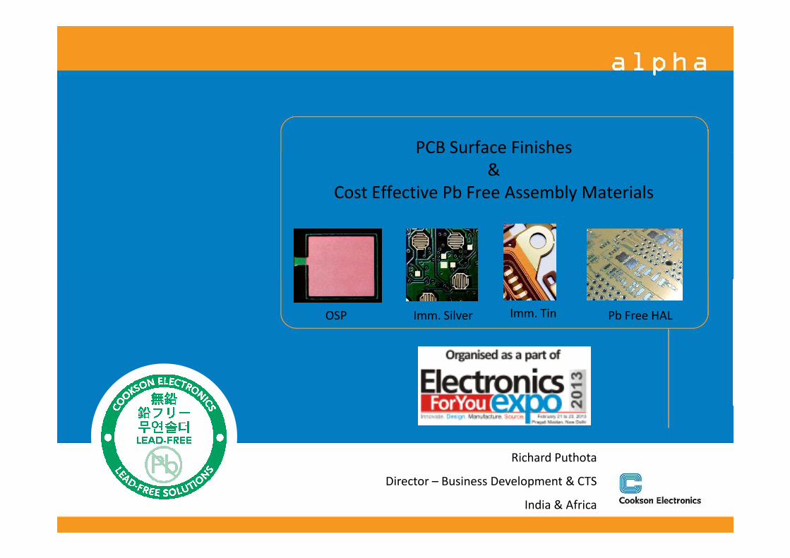
PCB Surface Finishes
&
Cost Effective Pb Free Assembly Materials
OSP Imm. TinImm. Silver Pb Free HAL
Richard Puthota
Director – Business Development & CTS
India & Africa
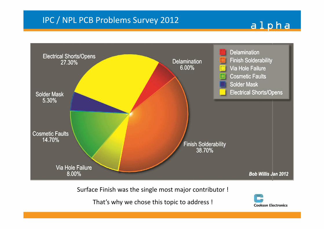
IPC / NPL PCB Problems Survey 2012
Surface Finish was the single most major contributor !
That’s why we chose this topic to address !
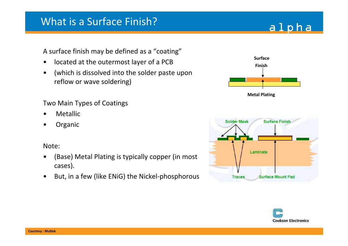
What is a Surface Finish?
A surface finish may be defined as a “coating”
• located at the outermost layer of a PCB
• (which is dissolved into the solder paste upon
reflow or wave soldering)
Two Main Types of Coatings
• Metallic
• Organic
Metal Plating
Finish
Surface
• Organic
Note:
• (Base) Metal Plating is typically copper (in most
cases).
• But, in a few (like ENiG) the Nickel-phosphorous
Courtesy : Multek
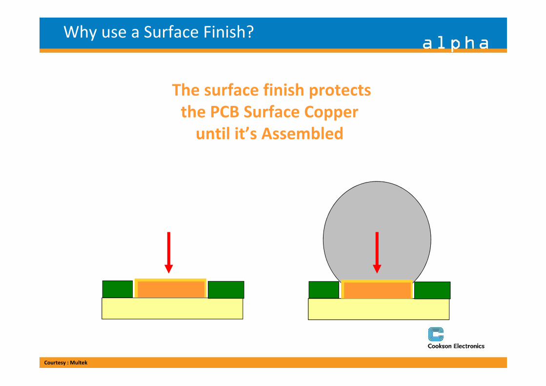
Why use a Surface Finish?
The surface finish protects
the PCB Surface Copper
until it’s Assembled
Courtesy : Multek
• Most important material decision made for the electronic assembly
• Influences the process yield, the amount of rework ,
field failure rate, the ability to test, the scrap rate, and of course
the cost.
• One can be lead astray by selecting the lowest cost surface finish
Importance of Surface Finish
• One can be lead astray by selecting the lowest cost surface finish
only to find that the total cost is much higher.
• The selection of a surface finish should be done with a holistic
approach that considers all important aspects of the assembly.
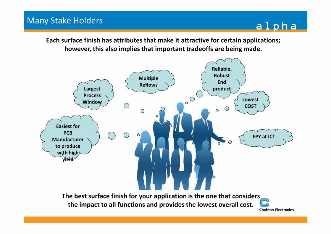
Each surface finish has attributes that make it attractive for certain applications;
however, this also implies that important tradeoffs are being made.
Lowest
COST
Largest
Process
Window
Reliable,
Robust
End
product
Multiple
Reflows
Many Stake Holders
Easiest for
PCB
Manufacturer
to produce
with high
yield
The best surface finish for your application is the one that considers
the impact to all functions and provides the lowest overall cost.
FPY at ICT
Which one to Choose ?
Options
Limitations
Advantages
Selection MetricCost
Advantages
How to Select a Proper Surface Finish?
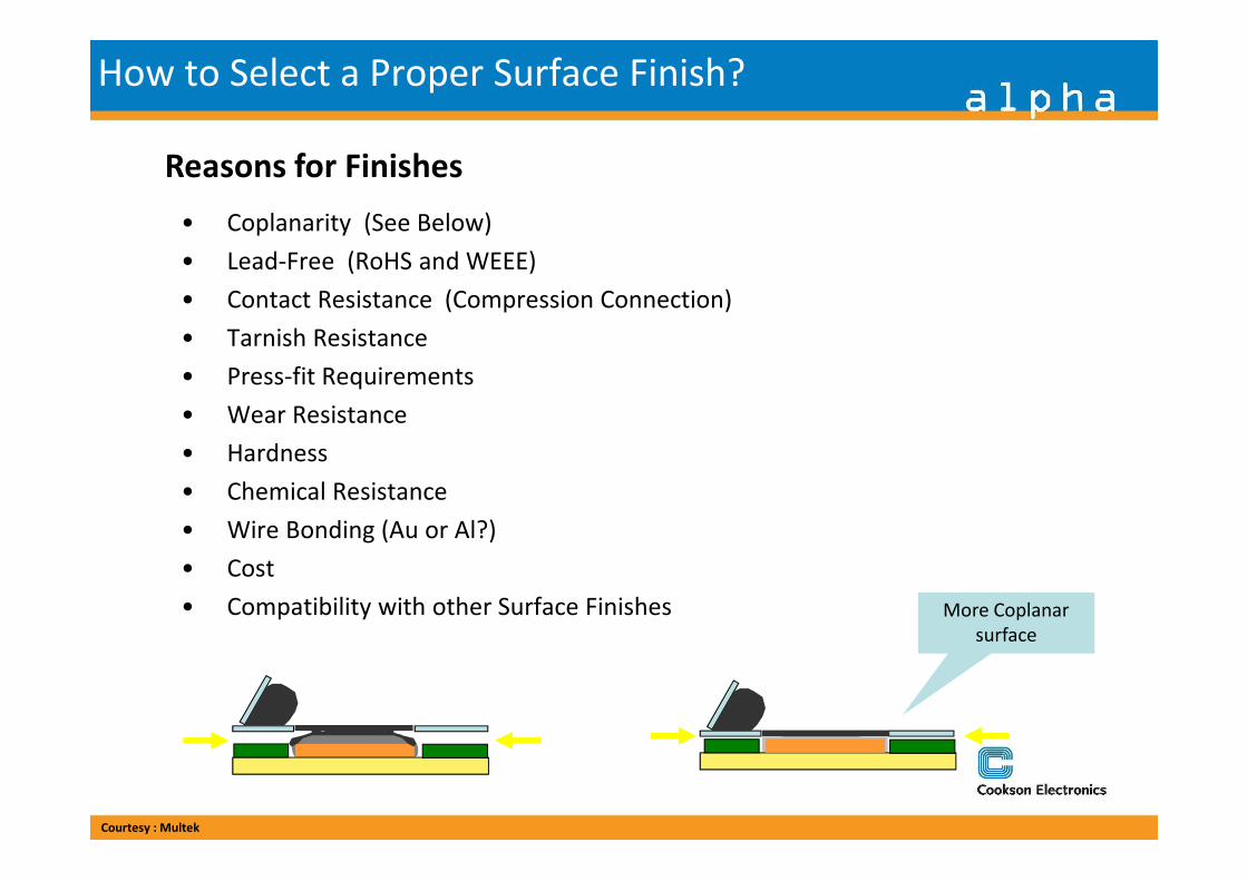
Reasons for Finishes
• Coplanarity (See Below)
• Lead-Free (RoHS and WEEE)
• Contact Resistance (Compression Connection)
• Tarnish Resistance
• Press-fit Requirements
• Wear Resistance
• Hardness• Hardness
• Chemical Resistance
• Wire Bonding (Au or Al?)
• Cost
• Compatibility with other Surface Finishes
Courtesy : Multek
More Coplanar
surface
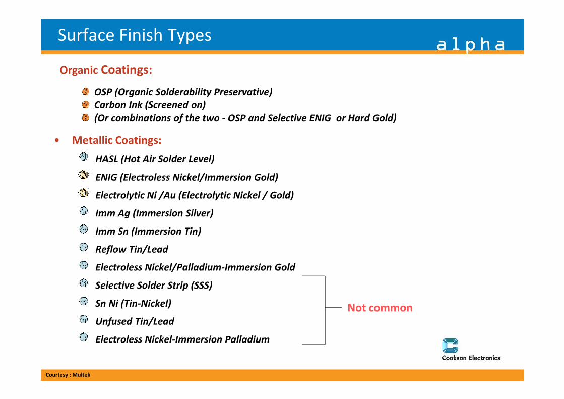
Surface Finish Types
• Metallic Coatings:
HASL (Hot Air Solder Level)
ENIG (Electroless Nickel/Immersion Gold)
Electrolytic Ni /Au (Electrolytic Nickel / Gold)
Organic Coatings:
OSP (Organic Solderability Preservative)
Carbon Ink (Screened on)
(Or combinations of the two - OSP and Selective ENIG or Hard Gold)
Electrolytic Ni /Au (Electrolytic Nickel / Gold)
Imm Ag (Immersion Silver)
Imm Sn (Immersion Tin)
Reflow Tin/Lead
Electroless Nickel/Palladium-Immersion Gold
Selective Solder Strip (SSS)
Sn Ni (Tin-Nickel)
Unfused Tin/Lead
Electroless Nickel-Immersion Palladium
Not common
Courtesy : Multek
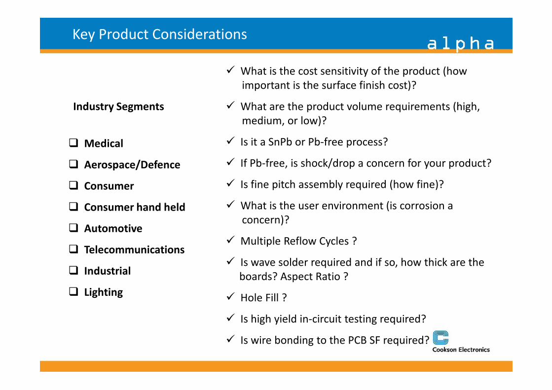
� Medical
� Aerospace/Defence
� Consumer
Key Product Considerations
� What is the cost sensitivity of the product (how
important is the surface finish cost)?
� What are the product volume requirements (high,
medium, or low)?
� Is it a SnPb or Pb-free process?
� If Pb-free, is shock/drop a concern for your product?
� Is fine pitch assembly required (how fine)?
Industry Segments
� Consumer hand held
� Automotive
� Telecommunications
� Industrial
� Lighting
� What is the user environment (is corrosion a
concern)?
� Multiple Reflow Cycles ?
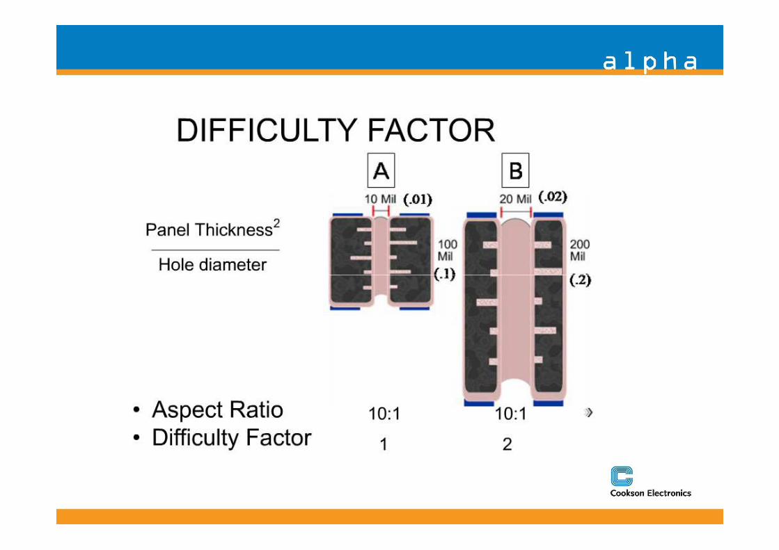
� Is wave solder required and if so, how thick are the
boards? Aspect Ratio ?
� Hole Fill ?
� Is high yield in-circuit testing required?
� Is wire bonding to the PCB SF required?
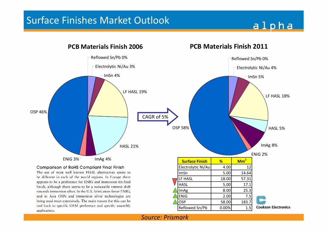
PCB Materials Finish 2011
Electrolytic Ni/Au 4%
ImSn 5%
LF HASL 18%
Reflowed Sn/Pb 0%
PCB Materials Finish 2006
Electrolytic Ni/Au 3%
ImSn 4%
LF HASL 19%
OSP 46%
Reflowed Sn/Pb 0%
CAGR of 5%
Surface Finishes Market Outlook
Source: Prismark
HASL 5%
ImAg 8%
ENiG 2%
OSP 58%
HASL 21%
ImAg 4%ENiG 3%Surface Finish % Mm
2
Electrolytic Ni/Au 4.00 12
ImSn 5.00 14.64
LF HASL 18.00 57.31
HASL 5.00 17.1
ImAg 8.00 25.3
ENiG 2.00 7.5
OSP 58.00 183.7
Reflowed Sn/Pb 0.00% 1.5
CAGR of 5%
OSP (Organic Surface Preservative) emerging
as a popular alternate surface finishas a popular alternate surface finish
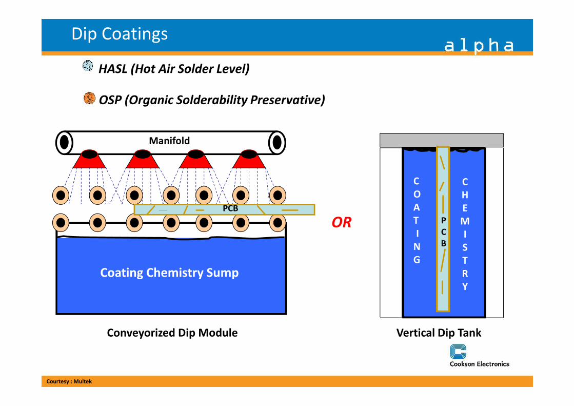
Dip Coatings
Manifold
PCB
HASL (Hot Air Solder Level)
OSP (Organic Solderability Preservative)
C
H
E
C
O
A
Vertical Dip TankConveyorized Dip Module
PCB
OR
Coating Chemistry Sump
E
M
I
S
T
R
Y
A
T
I
N
G
P
C
B
Courtesy : Multek
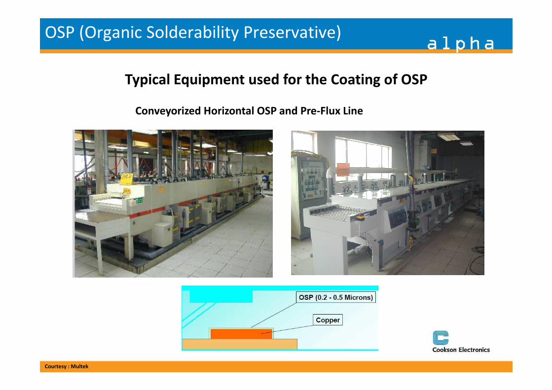
OSP (Organic Solderability Preservative)
Typical Equipment used for the Coating of OSP
Conveyorized Horizontal OSP and Pre-Flux Line
Courtesy : Multek
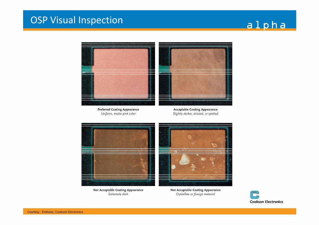
OSP Visual Inspection
Courtesy : Enthone, Cookson Electronics
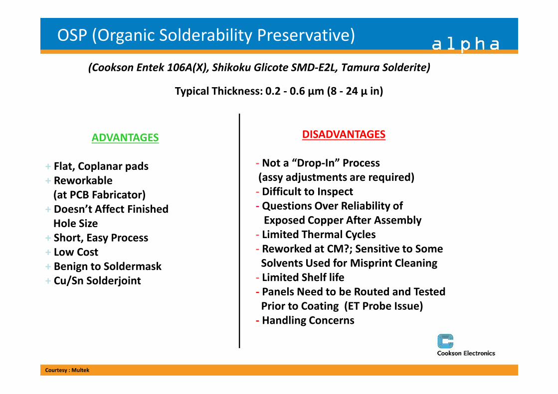
(Cookson Entek 106A(X), Shikoku Glicote SMD-E2L, Tamura Solderite)
ADVANTAGES
+ Flat, Coplanar pads
+ Reworkable
(at PCB Fabricator)
DISADVANTAGES
- Not a “Drop-In” Process
(assy adjustments are required)
- Difficult to Inspect
Typical Thickness: 0.2 - 0.6 µm (8 - 24 µ in)
OSP (Organic Solderability Preservative)
(at PCB Fabricator)
+ Doesn’t Affect Finished
Hole Size
+ Short, Easy Process
+ Low Cost
+ Benign to Soldermask
+ Cu/Sn Solderjoint
- Difficult to Inspect
- Questions Over Reliability of
Exposed Copper After Assembly
- Limited Thermal Cycles
- Reworked at CM?; Sensitive to Some
Solvents Used for Misprint Cleaning
- Limited Shelf life
- Panels Need to be Routed and Tested
Prior to Coating (ET Probe Issue)
- Handling Concerns
Courtesy : Multek
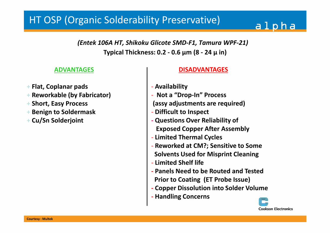
(Entek 106A HT, Shikoku Glicote SMD-F1, Tamura WPF-21)
ADVANTAGES
+ Flat, Coplanar pads
+ Reworkable (by Fabricator)
+ Short, Easy Process
+ Benign to Soldermask
+ Cu/Sn Solderjoint
DISADVANTAGES
- Availability
- Not a “Drop-In” Process
(assy adjustments are required)
- Difficult to Inspect
- Questions Over Reliability of
Typical Thickness: 0.2 - 0.6 µm (8 - 24 µ in)
HT OSP (Organic Solderability Preservative)
+ Cu/Sn Solderjoint - Questions Over Reliability of
Exposed Copper After Assembly
- Limited Thermal Cycles
- Reworked at CM?; Sensitive to Some
Solvents Used for Misprint Cleaning
- Limited Shelf life
- Panels Need to be Routed and Tested
Prior to Coating (ET Probe Issue)
- Copper Dissolution into Solder Volume
- Handling Concerns
Courtesy : Multek
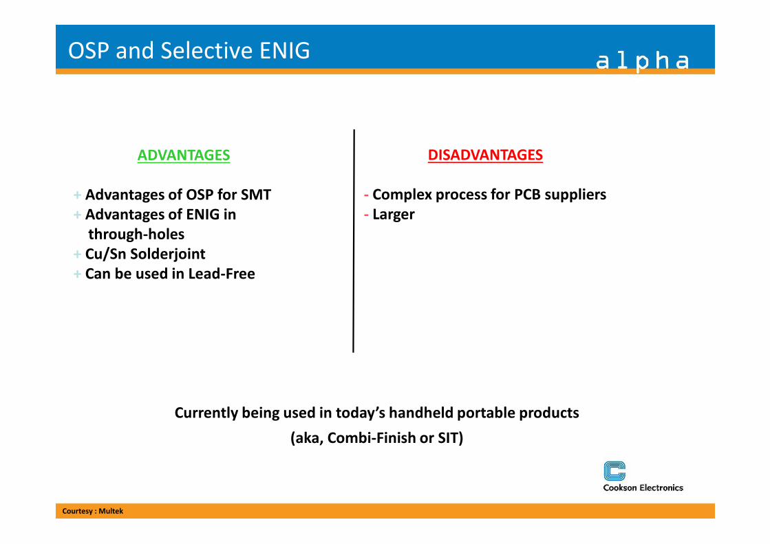
OSP and Selective ENIG
ADVANTAGES
+ Advantages of OSP for SMT
+ Advantages of ENIG in
through-holes
+ Cu/Sn Solderjoint
+ Can be used in Lead-Free
DISADVANTAGES
- Complex process for PCB suppliers
- Larger
+ Can be used in Lead-Free
Currently being used in today’s handheld portable products
(aka, Combi-Finish or SIT)
Courtesy : Multek
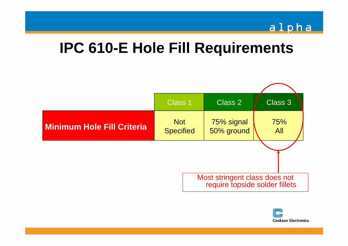
IPC 610-E Hole Fill Requirements
Class 1 Class 2 Class 3
Minimum Hole Fill CriteriaNot 75% signal 75%
Most stringent class does not require topside solder fillets
Minimum Hole Fill CriteriaNot
Specified75% signal50% ground
75%All
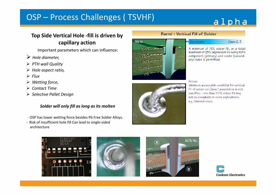
Top Side Vertical Hole -fill is driven by
capillary action
Important parameters which can influence:
� Hole diameter,
� PTH wall Quality
� Hole aspect ratio,
� Flux
� Wetting force,
� Contact Time
� Selective Pallet Design
OSP – Process Challenges ( TSVHF)
Solder will only fill as long as its molten
- OSP has lower wetting force besides Pb Free Solder Alloys.
- Risk of insufficient hole fill Can lead to single-sided
architecture
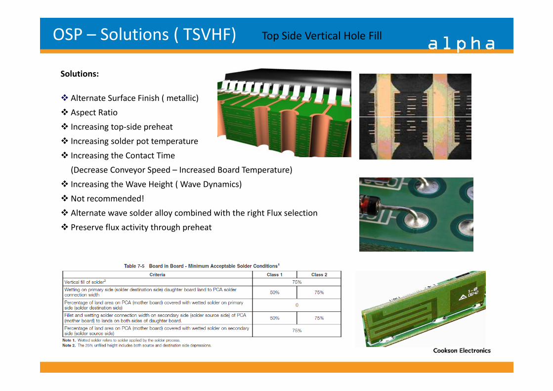
Solutions:
� Alternate Surface Finish ( metallic)
� Aspect Ratio
� Increasing top-side preheat
� Increasing solder pot temperature
� Increasing the Contact Time
(Decrease Conveyor Speed – Increased Board Temperature)
� Increasing the Wave Height ( Wave Dynamics)
� Not recommended!
OSP – Solutions ( TSVHF) Top Side Vertical Hole Fill
� Not recommended!
� Alternate wave solder alloy combined with the right Flux selection
� Preserve flux activity through preheat
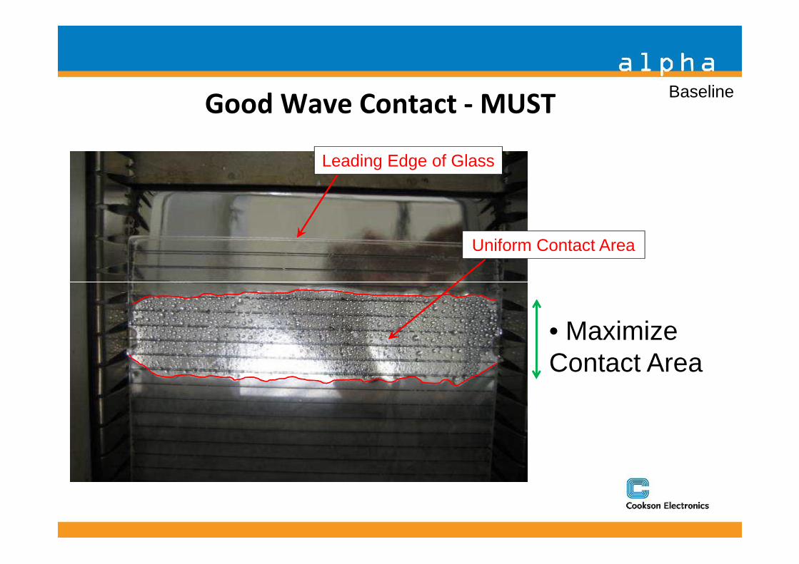
Good Wave Contact - MUST
Uniform Contact Area
Baseline
Leading Edge of Glass
• Maximize Contact Area
Enthone
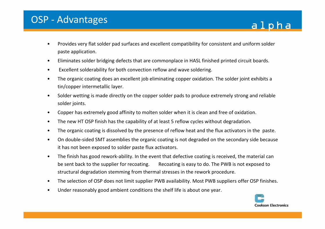
OSP - Advantages
• Provides very flat solder pad surfaces and excellent compatibility for consistent and uniform solder
paste application.
• Eliminates solder bridging defects that are commonplace in HASL finished printed circuit boards.
• Excellent solderability for both convection reflow and wave soldering.
• The organic coating does an excellent job eliminating copper oxidation. The solder joint exhibits a
tin/copper intermetallic layer.
• Solder wetting is made directly on the copper solder pads to produce extremely strong and reliable
solder joints.
• Copper has extremely good affinity to molten solder when it is clean and free of oxidation.• Copper has extremely good affinity to molten solder when it is clean and free of oxidation.
• The new HT OSP finish has the capability of at least 5 reflow cycles without degradation.
• The organic coating is dissolved by the presence of reflow heat and the flux activators in the paste.
• On double-sided SMT assemblies the organic coating is not degraded on the secondary side because
it has not been exposed to solder paste flux activators.
• The finish has good rework-ability. In the event that defective coating is received, the material can
be sent back to the supplier for recoating. Recoating is easy to do. The PWB is not exposed to
structural degradation stemming from thermal stresses in the rework procedure.
• The selection of OSP does not limit supplier PWB availability. Most PWB suppliers offer OSP finishes.
• Under reasonably good ambient conditions the shelf life is about one year.

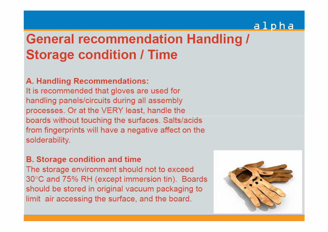
a. Careful material handling procedures must be followed. Gloves or finger cots must be worn to protect the
OSP coating material from fingerprints. Human salts are capable of degrading the coating such that the
solder ability of the copper will be compromised.
b. Strict practices and controls designed to eliminate misprinting of solder paste is paramount. Mechanical
removal of the solder paste causes solder particles to be spread and imbedded inside via holes. Chemical
removal of the paste degrades the organic coating. Alcohol and other alcohol-blended solvents dissolve
about 75% of the coating material over the copper. Water cleaning removes about 15%. Board assemblies
that have been treated with cleaning solvents to remove paste misprints must be processed with haste to
avoid non-wetting defects resulting from oxidized copper.
OSP Disadvantages
c. OSP finished printed circuit boards may not be suitable for RF circuitry assemblies. Most RF boards require a
metal shield to be soldered and in contact to the grounding trace, thus providing the necessary shielding. The
organic coating and the shield may not provide sufficient electrical shielding (no metal to metal contact).
d. The OSP material can give ICT test probes difficulty in contacting the test pads on the board. More expensive
multi-point test probes may be required in many cases. More frequent cleaning of the ICT test fixture probes
will be necessary. An alternative solution is to apply solder paste to the test pads to ensure positive contact.
This will not be possible if vias are used in place of test pads.
e. Interleaving paper should be used to protect the OSP coating from abrasion damage during transit, where
boards may slide against one other when stacked. An alternative method, and a more costly one, is to place
individual boards in plastic bags.
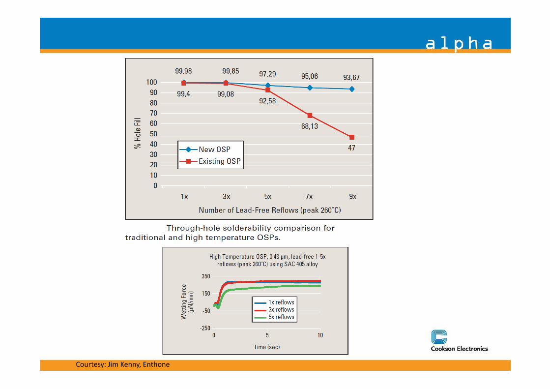
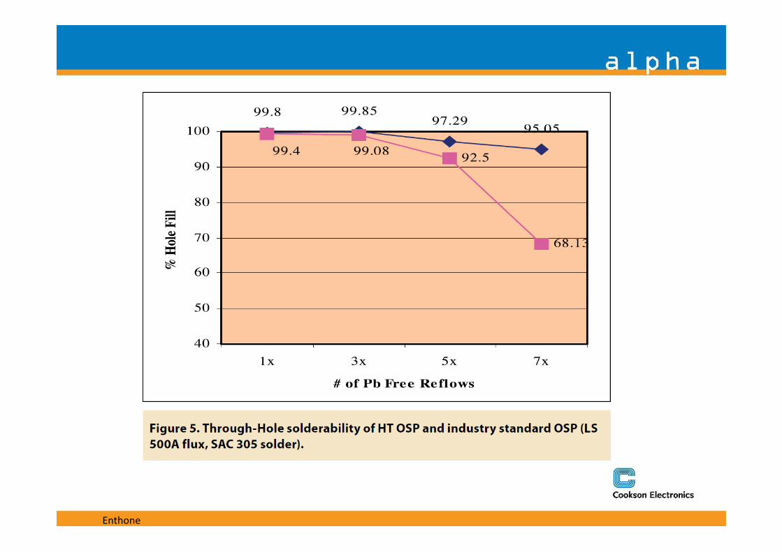
Courtesy: Jim Kenny, Enthone
HASL or HAL
Hot Air Solder Leveling
Or
Hot Air leveling
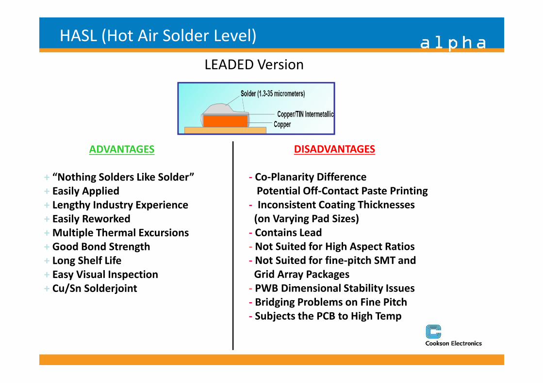
HASL (Hot Air Solder Level)
ADVANTAGES
+ “Nothing Solders Like Solder”
+ Easily Applied
DISADVANTAGES
- Co-Planarity Difference
Potential Off-Contact Paste Printing
LEADED Version
+ Easily Applied
+ Lengthy Industry Experience
+ Easily Reworked
+ Multiple Thermal Excursions
+ Good Bond Strength
+ Long Shelf Life
+ Easy Visual Inspection
+ Cu/Sn Solderjoint
Potential Off-Contact Paste Printing
- Inconsistent Coating Thicknesses
(on Varying Pad Sizes)
- Contains Lead
- Not Suited for High Aspect Ratios
- Not Suited for fine-pitch SMT and
Grid Array Packages
- PWB Dimensional Stability Issues
- Bridging Problems on Fine Pitch
- Subjects the PCB to High Temp
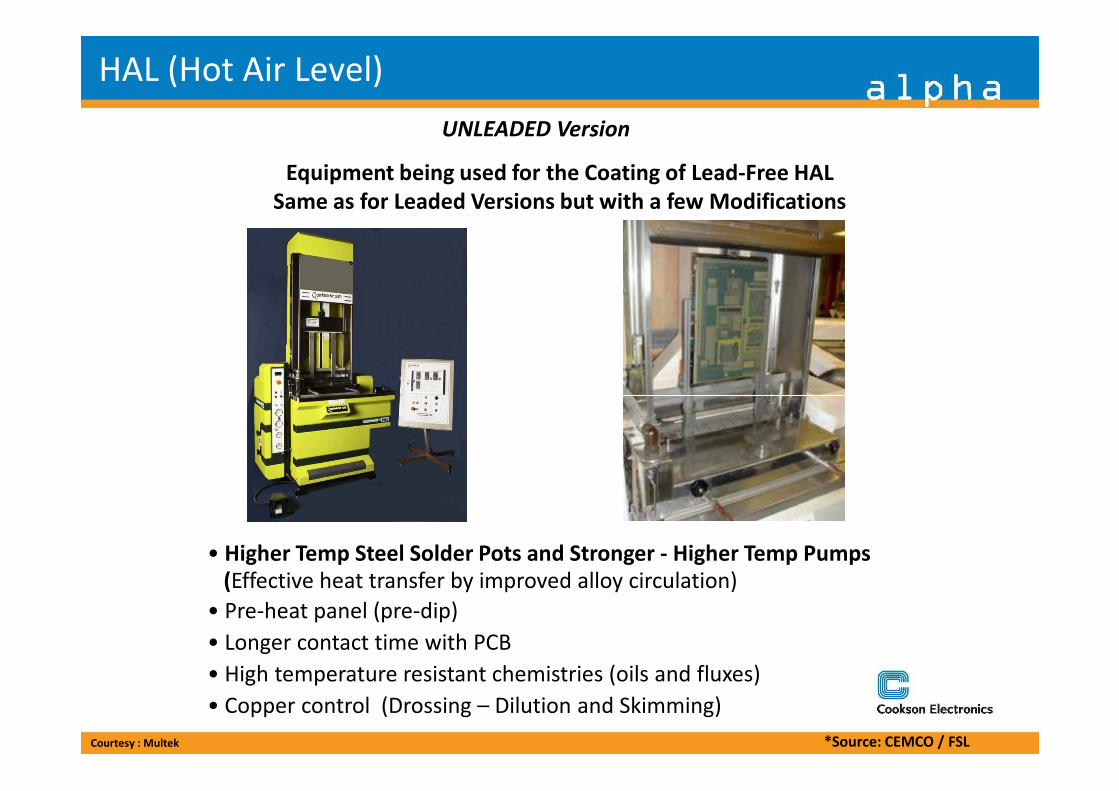
HAL (Hot Air Level)
Equipment being used for the Coating of Lead-Free HAL
Same as for Leaded Versions but with a few Modifications
UNLEADED Version
• Higher Temp Steel Solder Pots and Stronger - Higher Temp Pumps
(Effective heat transfer by improved alloy circulation)
• Pre-heat panel (pre-dip)
• Longer contact time with PCB
• High temperature resistant chemistries (oils and fluxes)
• Copper control (Drossing – Dilution and Skimming)
*Source: CEMCO / FSLCourtesy : Multek
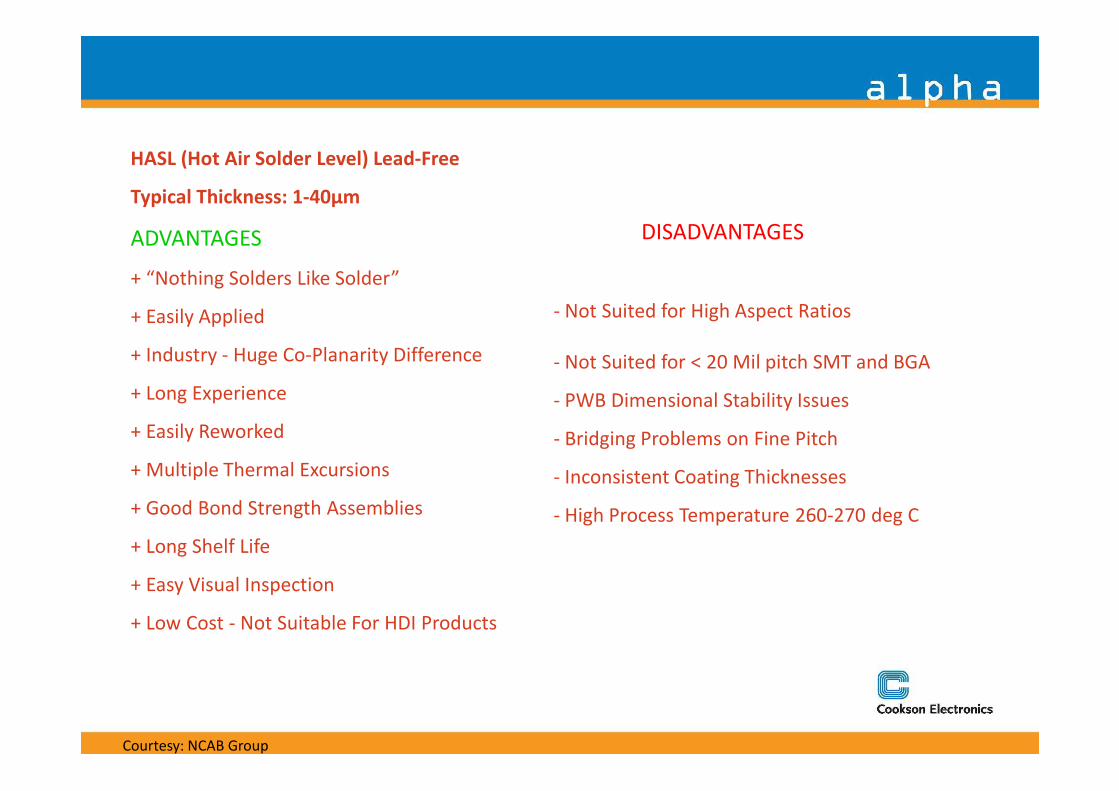
HASL (Hot Air Solder Level) Lead-Free
Typical Thickness: 1-40μm
ADVANTAGES
+ “Nothing Solders Like Solder”
+ Easily Applied
+ Industry - Huge Co-Planarity Difference
+ Long Experience
- Not Suited for High Aspect Ratios
- Not Suited for < 20 Mil pitch SMT and BGA
- PWB Dimensional Stability Issues
DISADVANTAGES
+ Long Experience
+ Easily Reworked
+ Multiple Thermal Excursions
+ Good Bond Strength Assemblies
+ Long Shelf Life
+ Easy Visual Inspection
+ Low Cost - Not Suitable For HDI Products
Courtesy: NCAB Group
- PWB Dimensional Stability Issues
- Bridging Problems on Fine Pitch
- Inconsistent Coating Thicknesses
- High Process Temperature 260-270 deg C
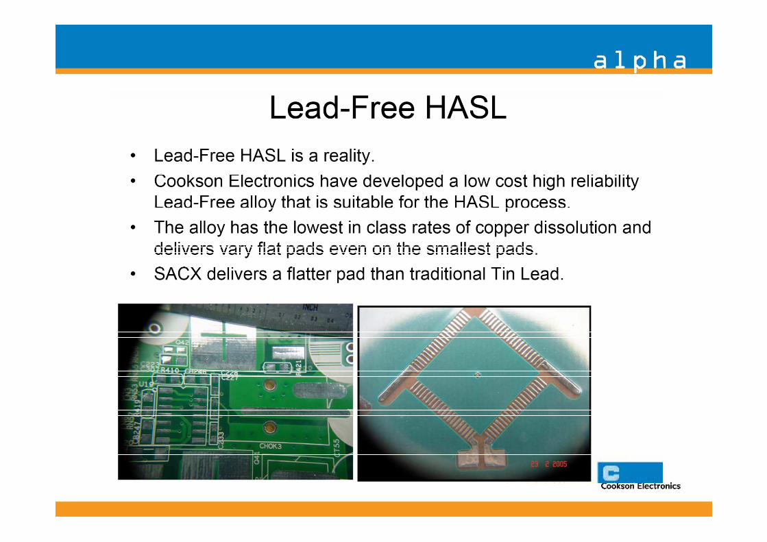
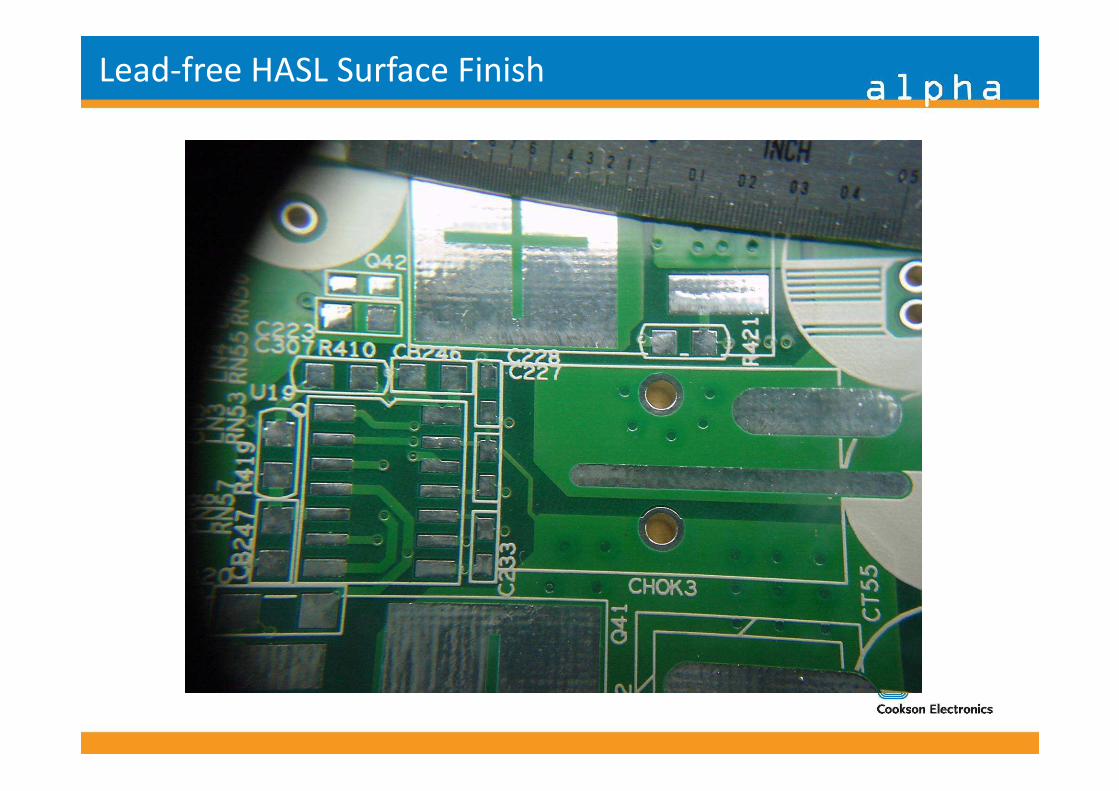
Lead-free HASL Surface Finish
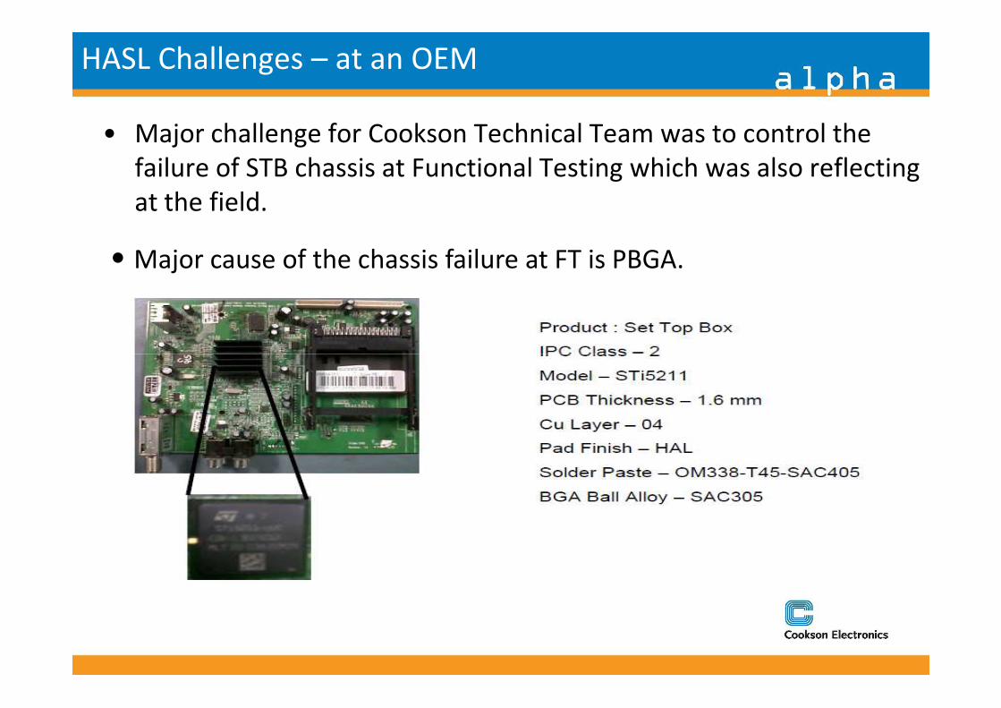
HASL Challenges – at an OEM
• Major challenge for Cookson Technical Team was to control the
failure of STB chassis at Functional Testing which was also reflecting
at the field.
• Major cause of the chassis failure at FT is PBGA.
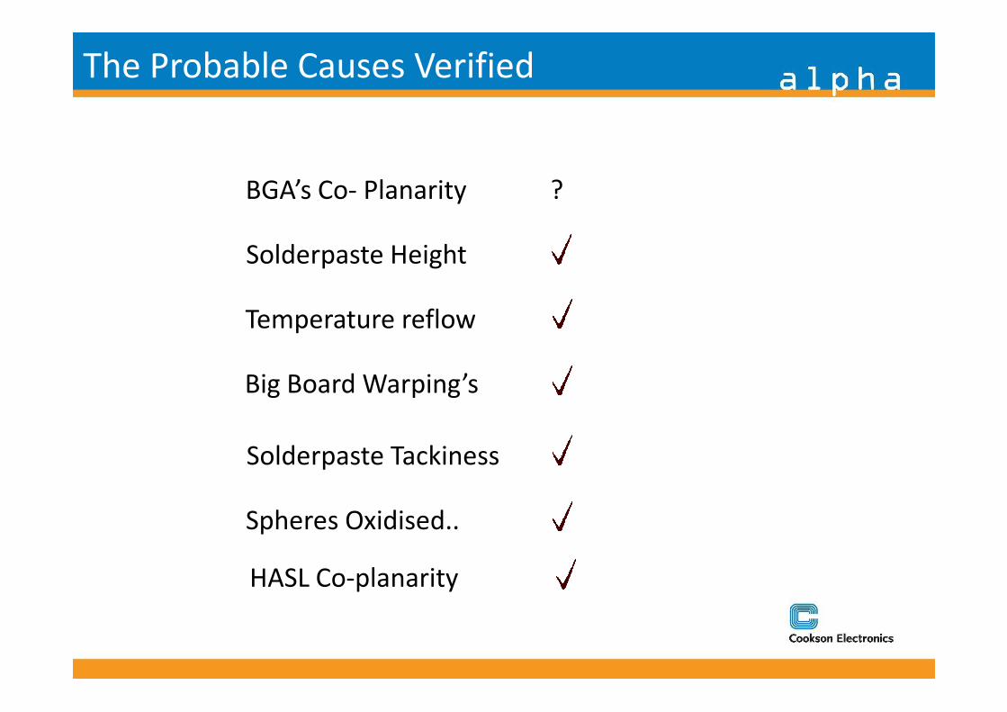
The Probable Causes Verified
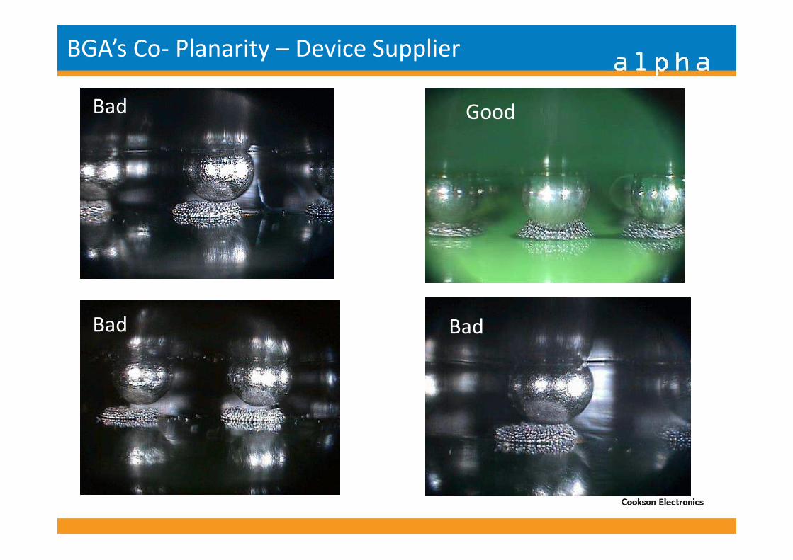
BGA’s Co- Planarity ?
Solderpaste Height
Temperature reflow
Solderpaste Tackiness
Spheres Oxidised..
Big Board Warping’s
HASL Co-planarity
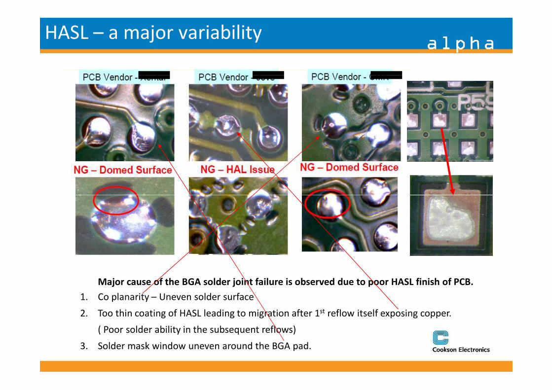
HASL – a major variability
Major cause of the BGA solder joint failure is observed due to poor HASL finish of PCB.
1. Co planarity – Uneven solder surface
2. Too thin coating of HASL leading to migration after 1st reflow itself exposing copper.
( Poor solder ability in the subsequent reflows)
3. Solder mask window uneven around the BGA pad.
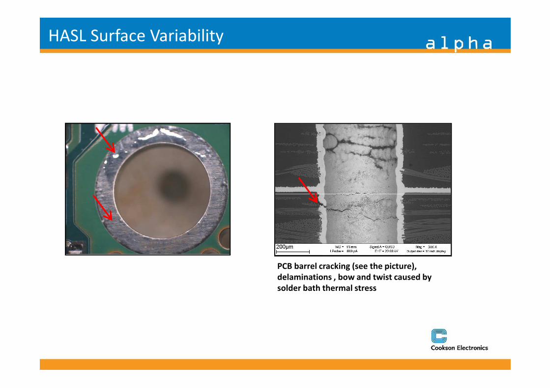
HASL Surface Variability
PCB barrel cracking (see the picture),
delaminations , bow and twist caused by
solder bath thermal stress
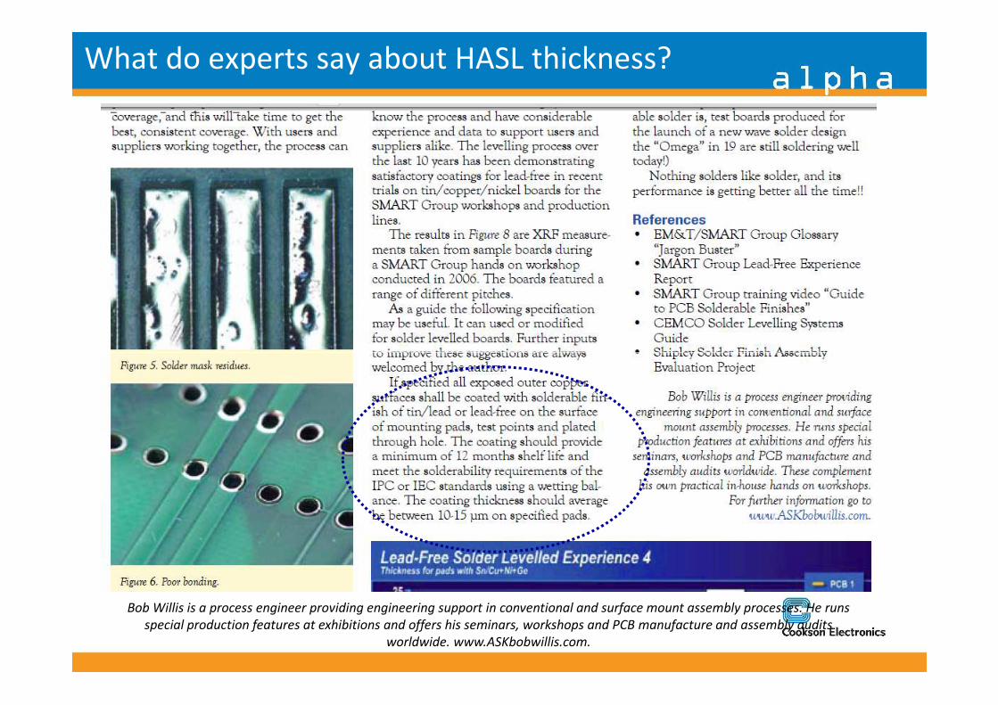
What do experts say about HASL thickness?
Bob Willis is a process engineer providing engineering support in conventional and surface mount assembly processes. He runs
special production features at exhibitions and offers his seminars, workshops and PCB manufacture and assembly audits
worldwide. www.ASKbobwillis.com.
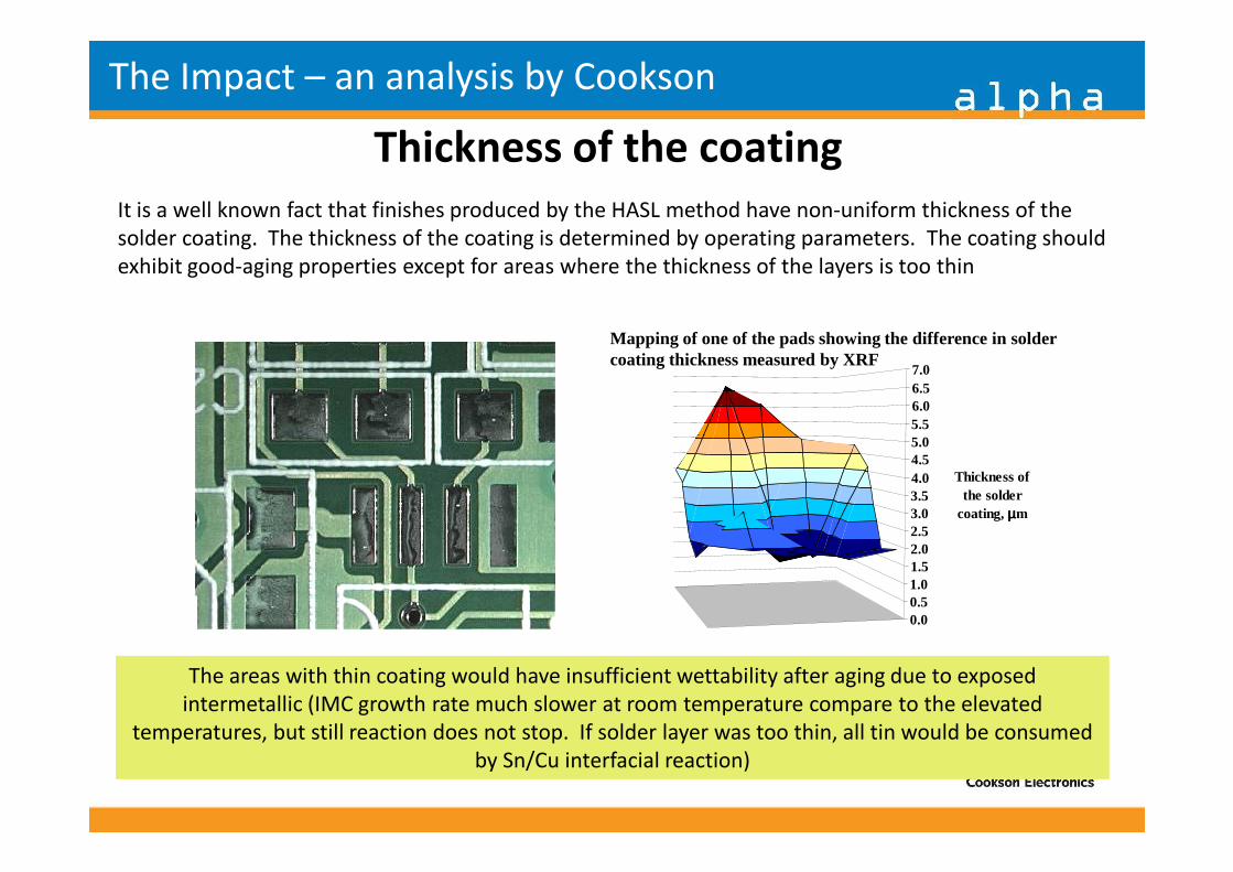
It is a well known fact that finishes produced by the HASL method have non-uniform thickness of the
solder coating. The thickness of the coating is determined by operating parameters. The coating should
exhibit good-aging properties except for areas where the thickness of the layers is too thin
5.05.56.06.57.0
Mapping of one of the pads showing the difference in solder coating thickness measured by XRF
Thickness of the coating
The Impact – an analysis by Cookson
0.00.51.01.52.02.53.03.54.04.55.0
Thickness of the solder
coating, µµµµm
The areas with thin coating would have insufficient wettability after aging due to exposed
intermetallic (IMC growth rate much slower at room temperature compare to the elevated
temperatures, but still reaction does not stop. If solder layer was too thin, all tin would be consumed
by Sn/Cu interfacial reaction)
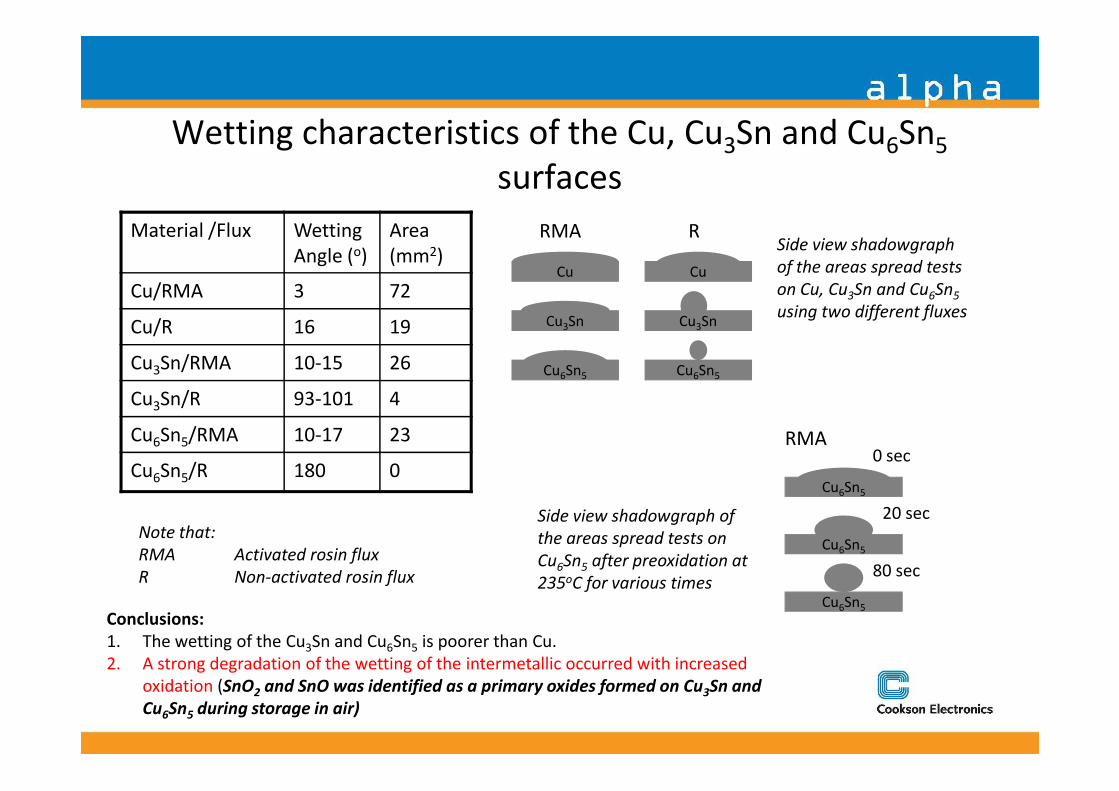
Wetting characteristics of the Cu, Cu3Sn and Cu6Sn5
surfaces
Material /Flux Wetting
Angle (o)
Area
(mm2)
Cu/RMA 3 72
Cu/R 16 19
Cu3Sn/RMA 10-15 26
Cu Sn/R 93-101 4
Cu
Cu3Sn
Cu6Sn5
Cu
Cu3Sn
Cu6Sn5
RRMASide view shadowgraph
of the areas spread tests
on Cu, Cu3Sn and Cu6Sn5
using two different fluxes
Cu3Sn/R 93-101 4
Cu6Sn5/RMA 10-17 23
Cu6Sn5/R 180 0
Note that:
RMA Activated rosin flux
R Non-activated rosin flux
Cu6Sn5
Cu6Sn5
0 secRMA
Cu6Sn5
20 sec
80 sec
Side view shadowgraph of
the areas spread tests on
Cu6Sn5 after preoxidation at
235oC for various times
Conclusions:
1. The wetting of the Cu3Sn and Cu6Sn5 is poorer than Cu.
2. A strong degradation of the wetting of the intermetallic occurred with increased
oxidation (SnO2 and SnO was identified as a primary oxides formed on Cu3Sn and
Cu6Sn5 during storage in air)
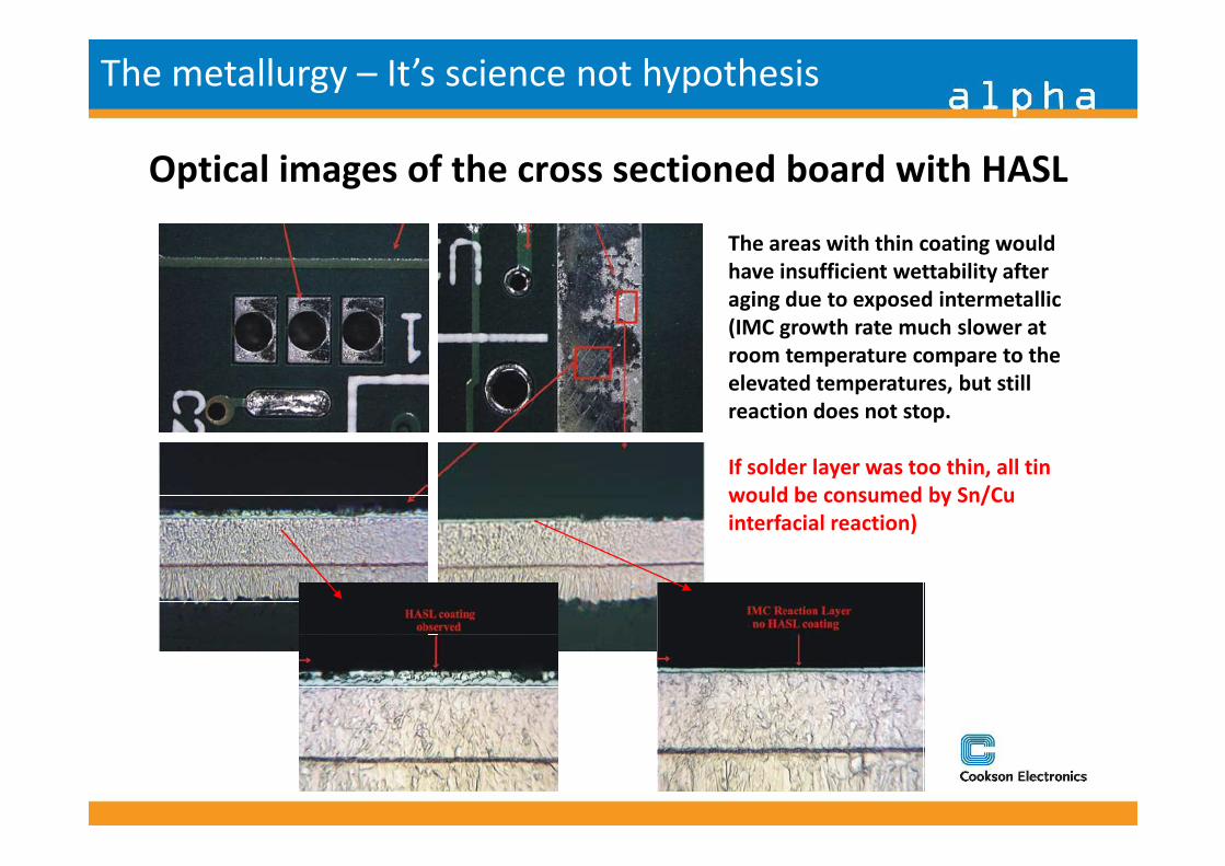
Optical images of the cross sectioned board with HASL
The areas with thin coating would
have insufficient wettability after
aging due to exposed intermetallic
(IMC growth rate much slower at
room temperature compare to the
elevated temperatures, but still
reaction does not stop.
The metallurgy – It’s science not hypothesis
If solder layer was too thin, all tin
would be consumed by Sn/Cu
interfacial reaction)
GoodBad
BGA’s Co- Planarity – Device Supplier
BadBad

What next ?
Alternate Finish ?
OSP ?OSP ?
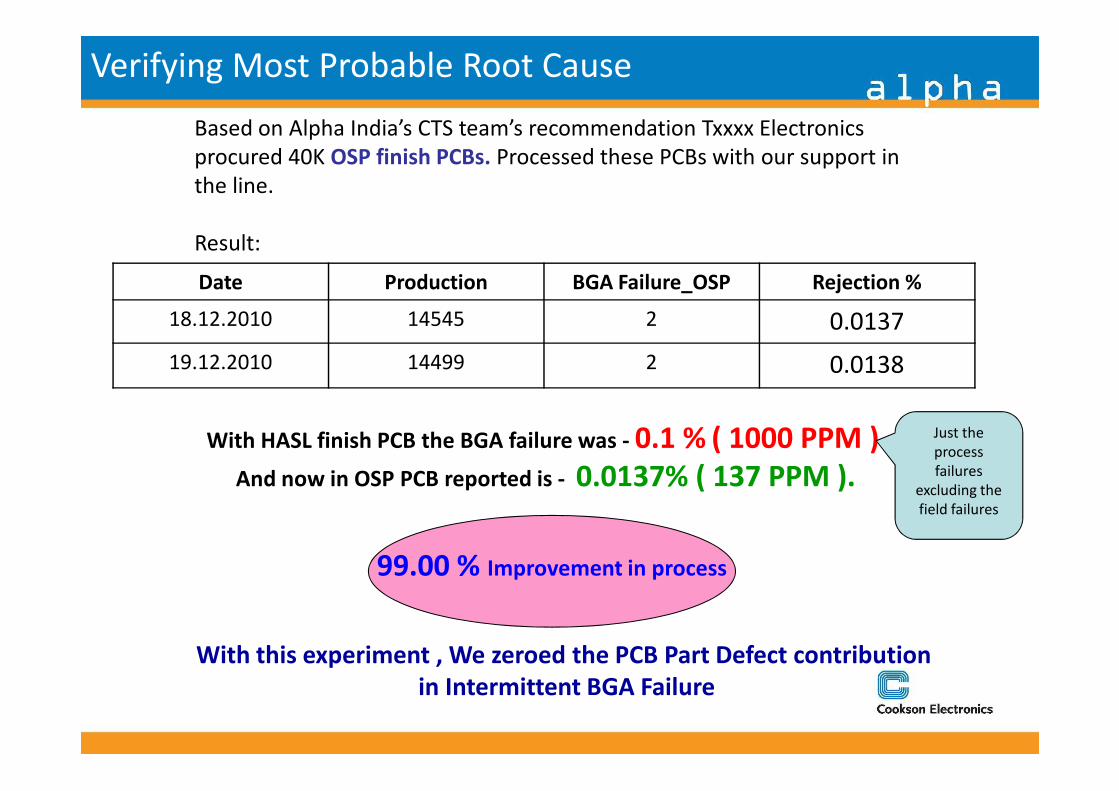
Based on Alpha India’s CTS team’s recommendation Txxxx Electronics
procured 40K OSP finish PCBs. Processed these PCBs with our support in
the line.
Result:
Date Production BGA Failure_OSP Rejection %
18.12.2010 14545 2 0.0137
19.12.2010 14499 2 0.0138
Verifying Most Probable Root Cause
With HASL finish PCB the BGA failure was - 0.1 % ( 1000 PPM )
And now in OSP PCB reported is - 0.0137% ( 137 PPM ).
With this experiment , We zeroed the PCB Part Defect contribution
in Intermittent BGA Failure
99.00 % Improvement in process
Just the
process
failures
excluding the
field failures
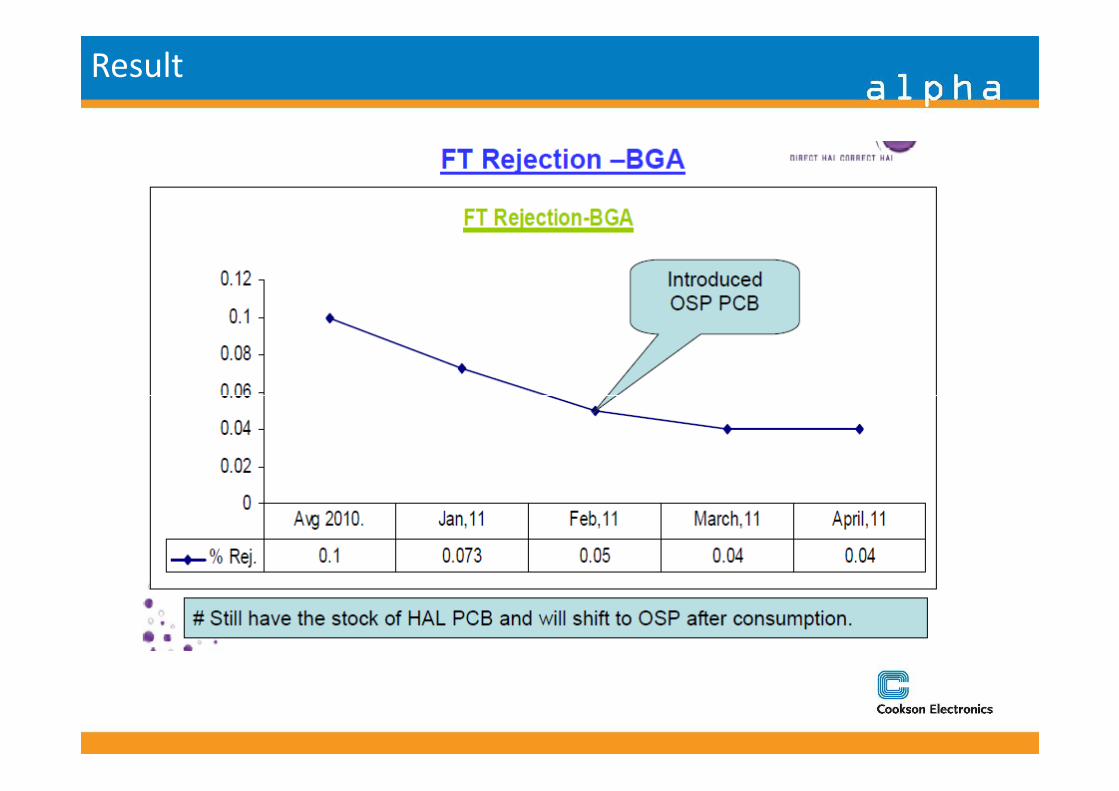
Result
ALLOY SYSTEM
COMPOSITION MELTING RANGE
(oC) Sn-3.5Ag 221 Sn-Ag Sn-2Ag 221-226
Sn-Cu Sn-0.7Cu 227 Sn-3.5Ag-3Bi 206-213 Sn-Ag-Bi Sn-7.5Bi-2Ag 207-212
Sn-3.8Ag-0.7Cu ~217 Sn-Ag-Cu
Lead-Free Solder Options
Sn-3.8Ag-0.7Cu ~217 Sn-4Ag-0.5Cu ~217
Sn-Ag-Cu Eutectic
Sn-4.7Ag-1.7Cu ~217 SAC305 Sn-3.0Ag-0.5Cu 218-219?
SACX0307 Sn~0.9Cu~0.17Ag~0.14Bi 217-228 Sn-Ag-Cu-Sb Sn-2Ag-0.8Cu-0.5Sb 216-222
Sn-Zn-Bi Sn-7Zn-5Bi 170-190
EUTECTIC ALLOYS
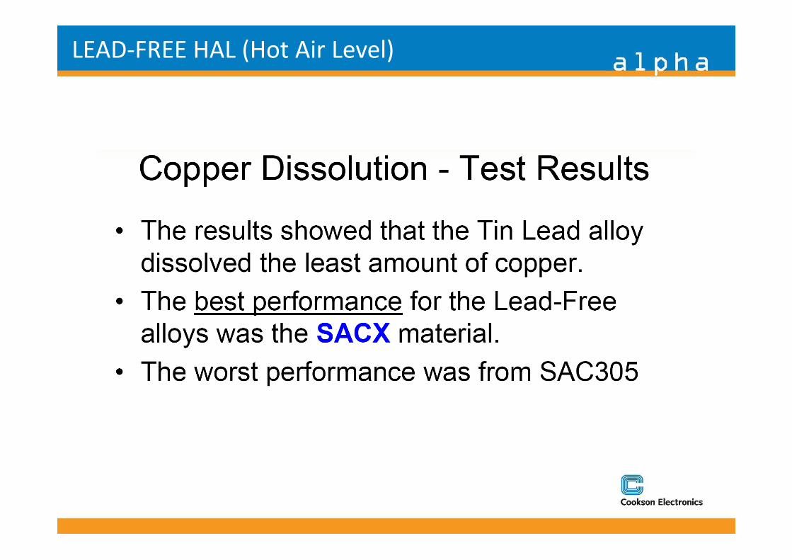
LEAD-FREE HAL (Hot Air Level)
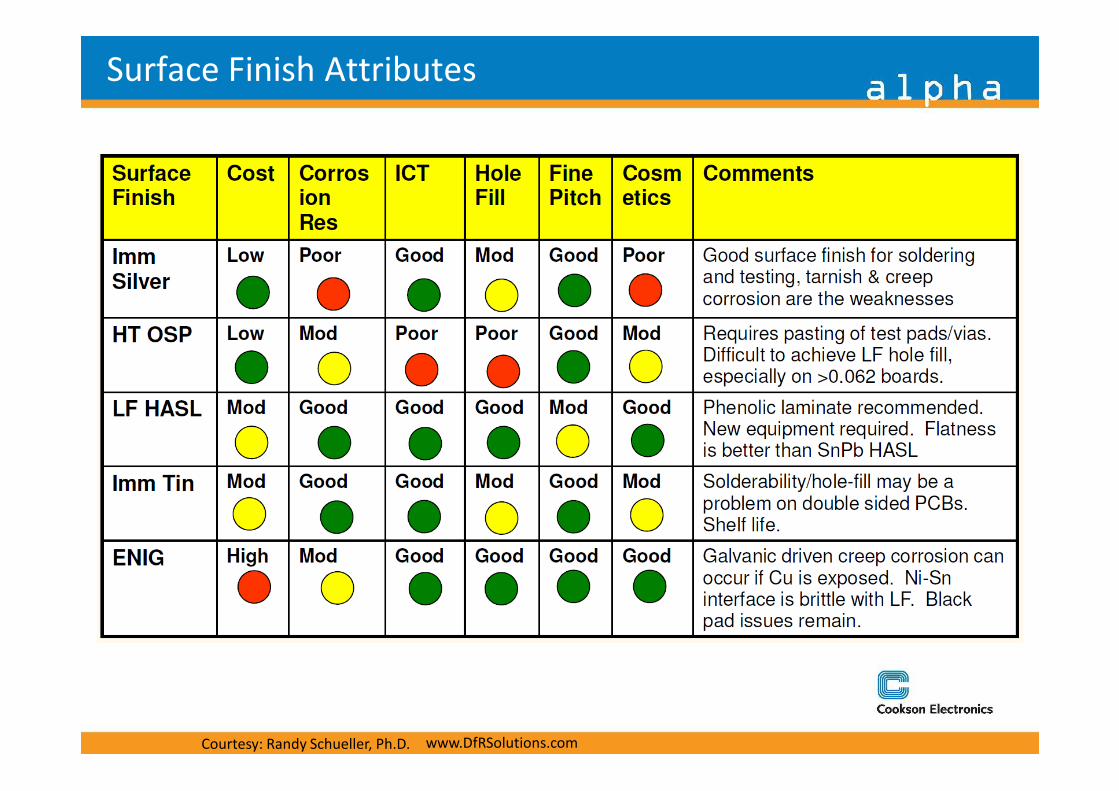
Surface Finish Attributes
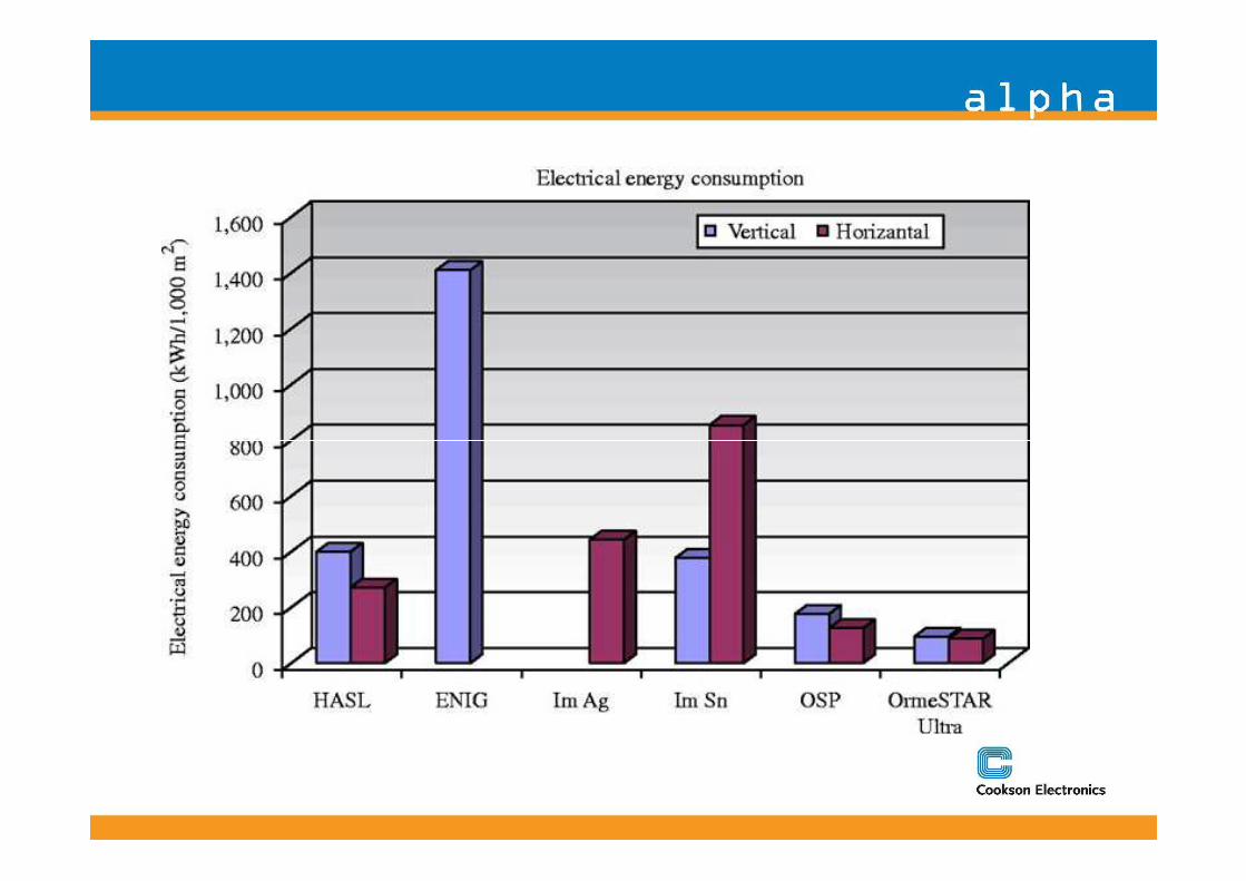
www.DfRSolutions.comCourtesy: Randy Schueller, Ph.D.
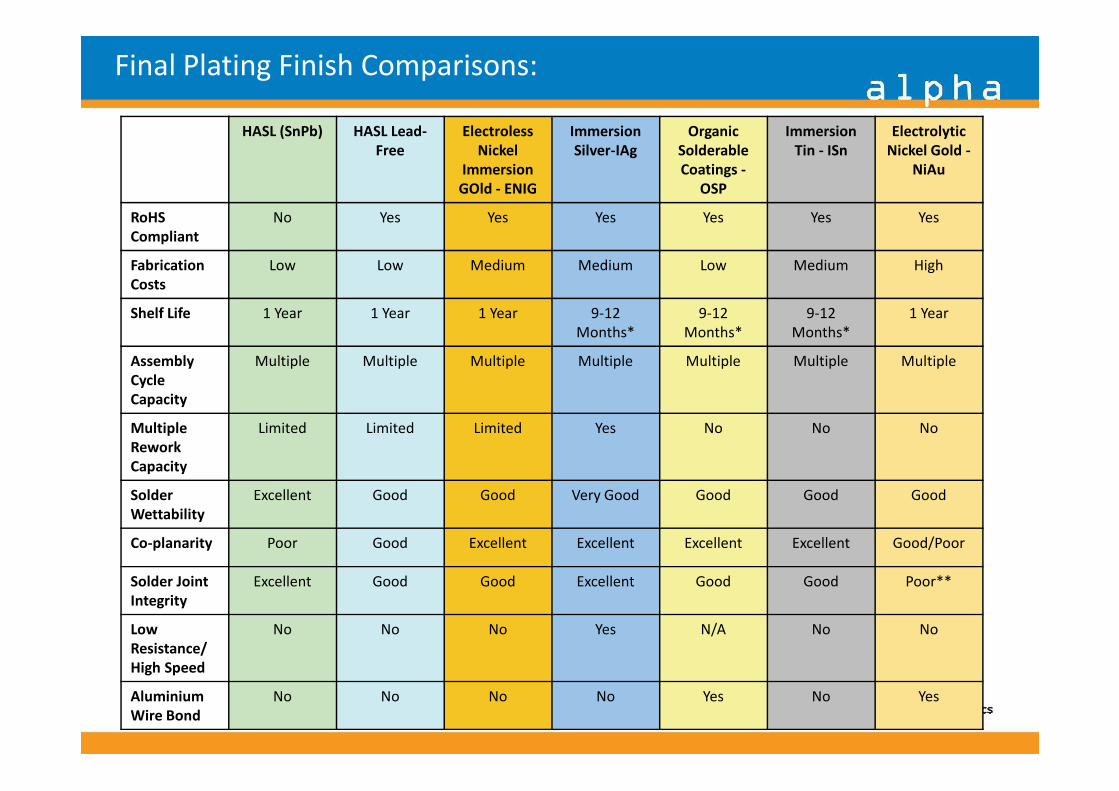
Final Plating Finish Comparisons:
HASL (SnPb) HASL Lead-
Free
Electroless
Nickel
Immersion
GOld - ENIG
Immersion
Silver-IAg
Organic
Solderable
Coatings -
OSP
Immersion
Tin - ISn
Electrolytic
Nickel Gold -
NiAu
RoHS
Compliant
No Yes Yes Yes Yes Yes Yes
Fabrication
Costs
Low Low Medium Medium Low Medium High
Shelf Life 1 Year 1 Year 1 Year 9-12
Months*
9-12
Months*
9-12
Months*
1 Year
Assembly
Cycle
Capacity
Multiple Multiple Multiple Multiple Multiple Multiple Multiple
Capacity
Multiple
Rework
Capacity
Limited Limited Limited Yes No No No
Solder
Wettability
Excellent Good Good Very Good Good Good Good
Co-planarity Poor Good Excellent Excellent Excellent Excellent Good/Poor
Solder Joint
Integrity
Excellent Good Good Excellent Good Good Poor**
Low
Resistance/
High Speed
No No No Yes N/A No No
Aluminium
Wire Bond
No No No No Yes No Yes
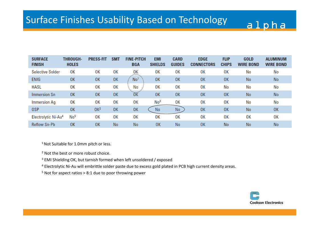
Surface Finishes Usability Based on Technology
1 Not Suitable for 1.0mm pitch or less.
2 Not the best or more robust choice.
3 EMI Shielding OK, but tarnish formed when left unsoldered / exposed
4 Electrolytic Ni-Au will embrittle solder paste due to excess gold plated in PCB high current density areas.
5 Not for aspect ratios > 8:1 due to poor throwing power
ENIG or ENEPIG
• SnPb medical and aerospace
• Small specialty electronics (not Pb-free that is susceptible to shock).
OSP (but must address ICT issues)
• Hand held electronics
Examples of Best Fit SF
• Hand held electronics
• Notebook computers
• Basic desktop computers
• Basic consumer electronics & power supplies
• Pb-free Medical or aerospace (thin PCBs)
ImAg
• Fully enclosed hand held electronics
• Basic consumer electronics
ImSn
• Simple consumer electronics (not fully enclosed)
• Simple medical or aerospace applications (1 side)
Examples of Best Fit SF
• Simple medical or aerospace applications (1 side)
• Low to moderate volume peripheral components
LF HASL
• Thick LF PCBs going into business environments
(servers, telecom equipment)
• Complex Pb-Free medical or aerospace?
Alternate Cost Effective Soldering
MaterialsMaterials
Wave Solder Materials
AlloysAlloys
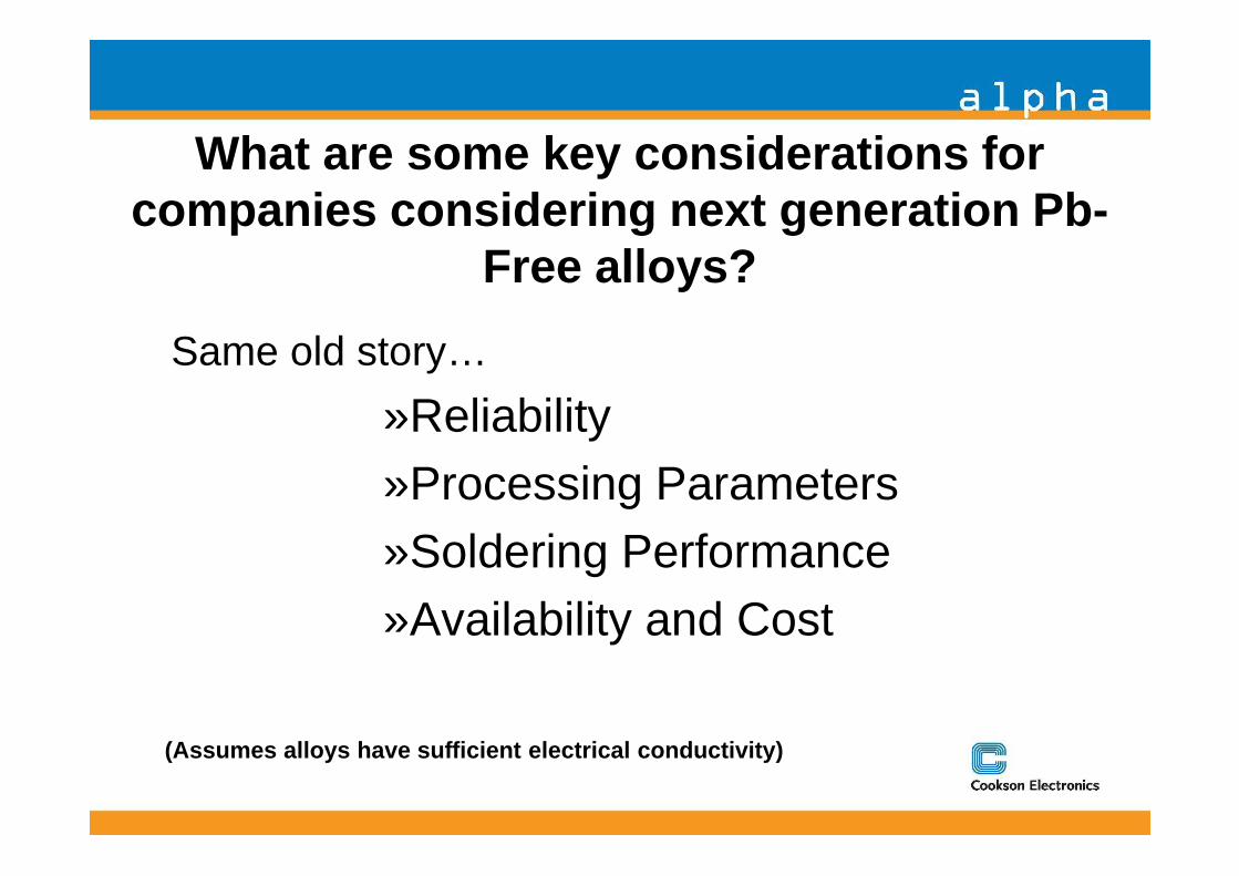
What are some key considerations for companies considering next generation Pb -
Free alloys?
Same old story…
»Reliability»Reliability»Processing Parameters »Soldering Performance»Availability and Cost
(Assumes alloys have sufficient electrical conducti vity)
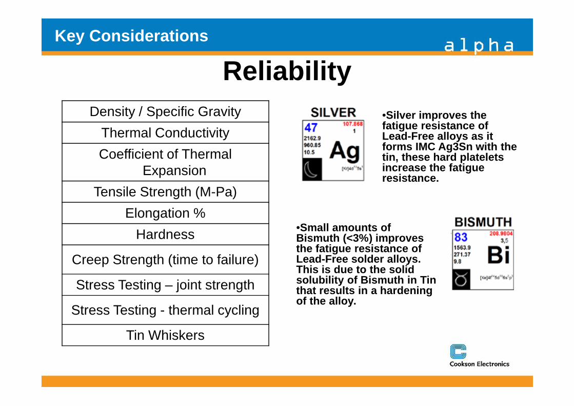
ReliabilityDensity / Specific Gravity
Thermal Conductivity
Coefficient of Thermal Expansion
Tensile Strength (M-Pa)
Key Considerations
•Silver improves the fatigue resistance of Lead-Free alloys as it forms IMC Ag3Sn with the tin, these hard platelets increase the fatigue resistance.
Elongation %
Hardness
Creep Strength (time to failure)
Stress Testing – joint strength
Stress Testing - thermal cycling
Tin Whiskers
•Small amounts of Bismuth (<3%) improves the fatigue resistance of Lead-Free solder alloys. This is due to the solid solubility of Bismuth in Tin that results in a hardening of the alloy.
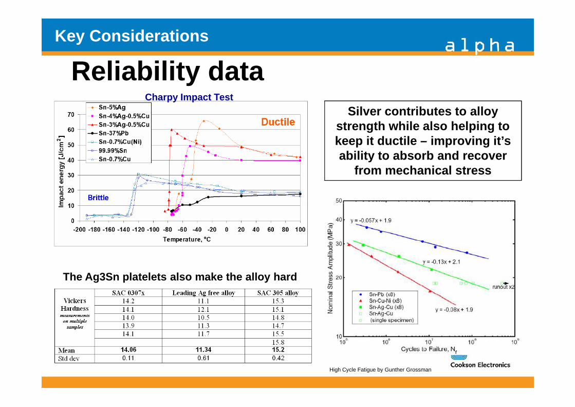
Reliability dataKey Considerations
Silver contributes to alloy strength while also helping to keep it ductile – improving it’s ability to absorb and recover
from mechanical stress
Charpy Impact Test
The Ag3Sn platelets also make the alloy hard
High Cycle Fatigue by Gunther Grossman
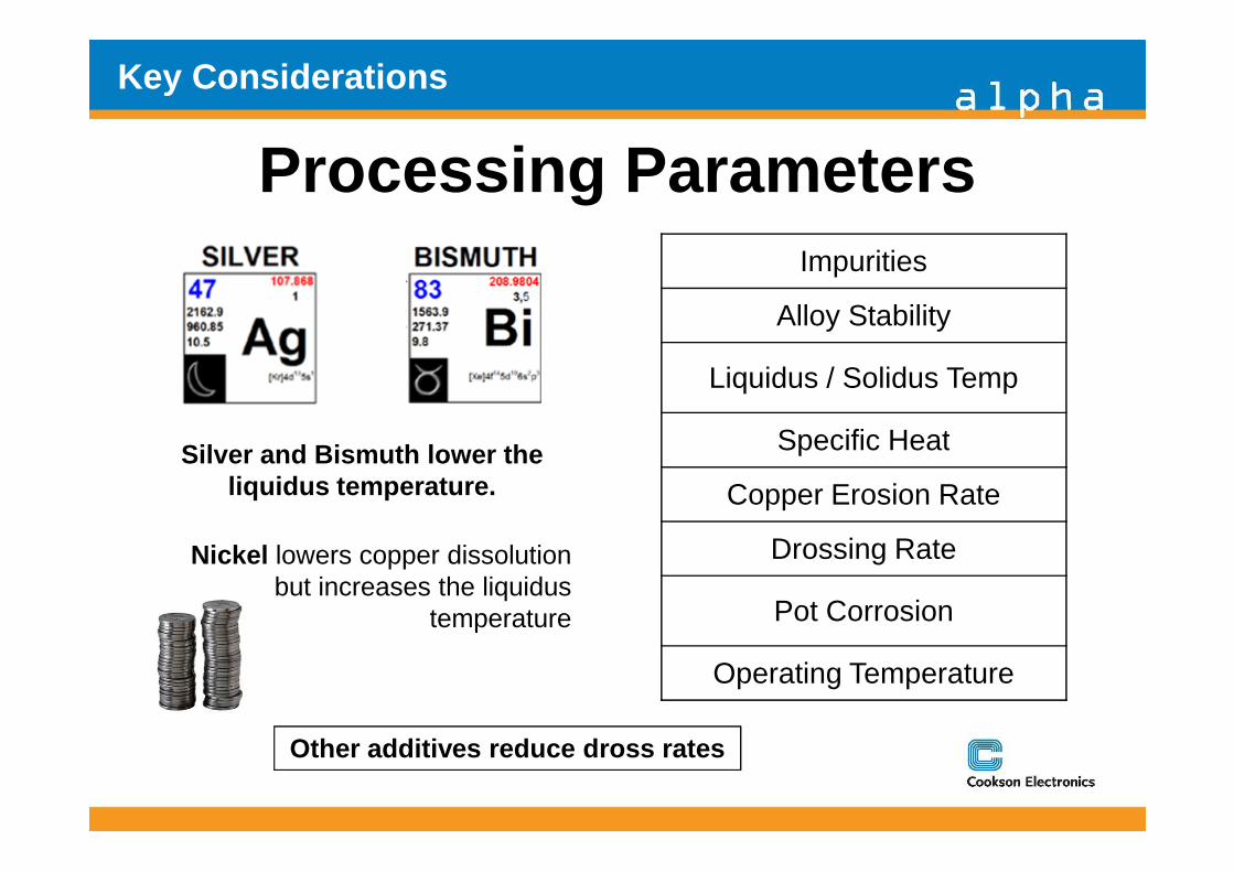
Processing ParametersImpurities
Alloy Stability
Liquidus / Solidus Temp
Specific Heat
Key Considerations
Specific Heat
Copper Erosion Rate
Drossing Rate
Pot Corrosion
Operating Temperature
Silver and Bismuth lower the liquidus temperature.
Nickel lowers copper dissolution but increases the liquidus
temperature
Other additives reduce dross rates
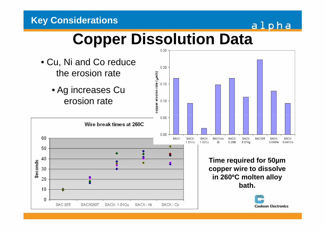
Copper Dissolution DataKey Considerations
• Cu, Ni and Co reduce the erosion rate
• Ag increases Cu erosion rate
Time required for 50µm copper wire to dissolve in 260ºC molten alloy
bath.
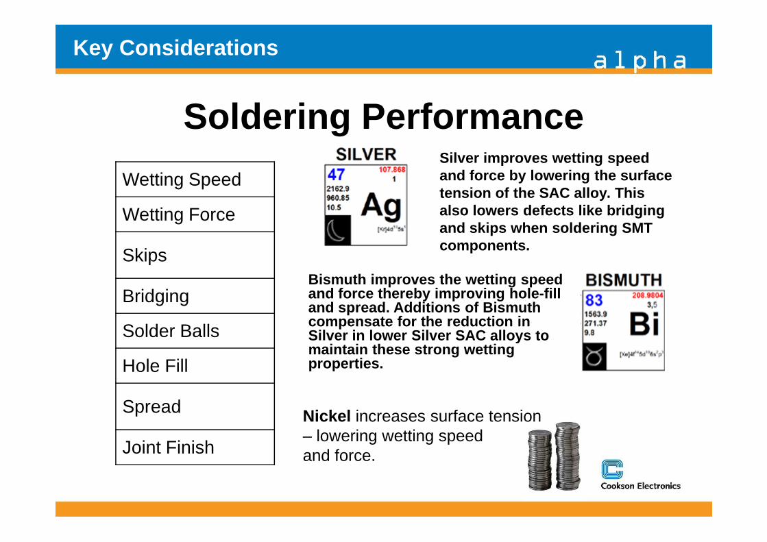
Soldering Performance
Wetting Speed
Wetting Force
Skips
Key Considerations
Silver improves wetting speed and force by lowering the surface tension of the SAC alloy. This also lowers defects like bridging and skips when soldering SMT components.
Bridging
Solder Balls
Hole Fill
Spread
Joint Finish
Bismuth improves the wetting speed and force thereby improving hole-fill and spread. Additions of Bismuth compensate for the reduction in Silver in lower Silver SAC alloys to maintain these strong wetting properties.
Nickel increases surface tension – lowering wetting speed and force.
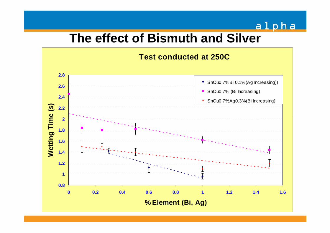
The effect of Bismuth and SilverTest conducted at 250C
2
2.2
2.4
2.6
2.8
Wet
ting
Tim
e (s
)
SnCu0.7%Bi 0.1%(Ag Increasing))
SnCu0.7% (Bi Increasing)
SnCu0.7%Ag0.3%(Bi Increasing)
0.8
1
1.2
1.4
1.6
1.8
2
0 0.2 0.4 0.6 0.8 1 1.2 1.4 1.6
% Element (Bi, Ag)
Wet
ting
Tim
e (s
)

Alloy Availability and CostAlloy availability
Alloy cost
Sizes / Shapes
Markings
Key Considerations
Is the alloy available everywhere you need it?
Packaging
Manufacturing proximity / capacity
Recycling
Regulatory
Intellectual Property
Silver content has big impact on alloy cost. A 1% decrease in silver results in a 10% decrease in cost.
Are all the alloys constituents recyclable?
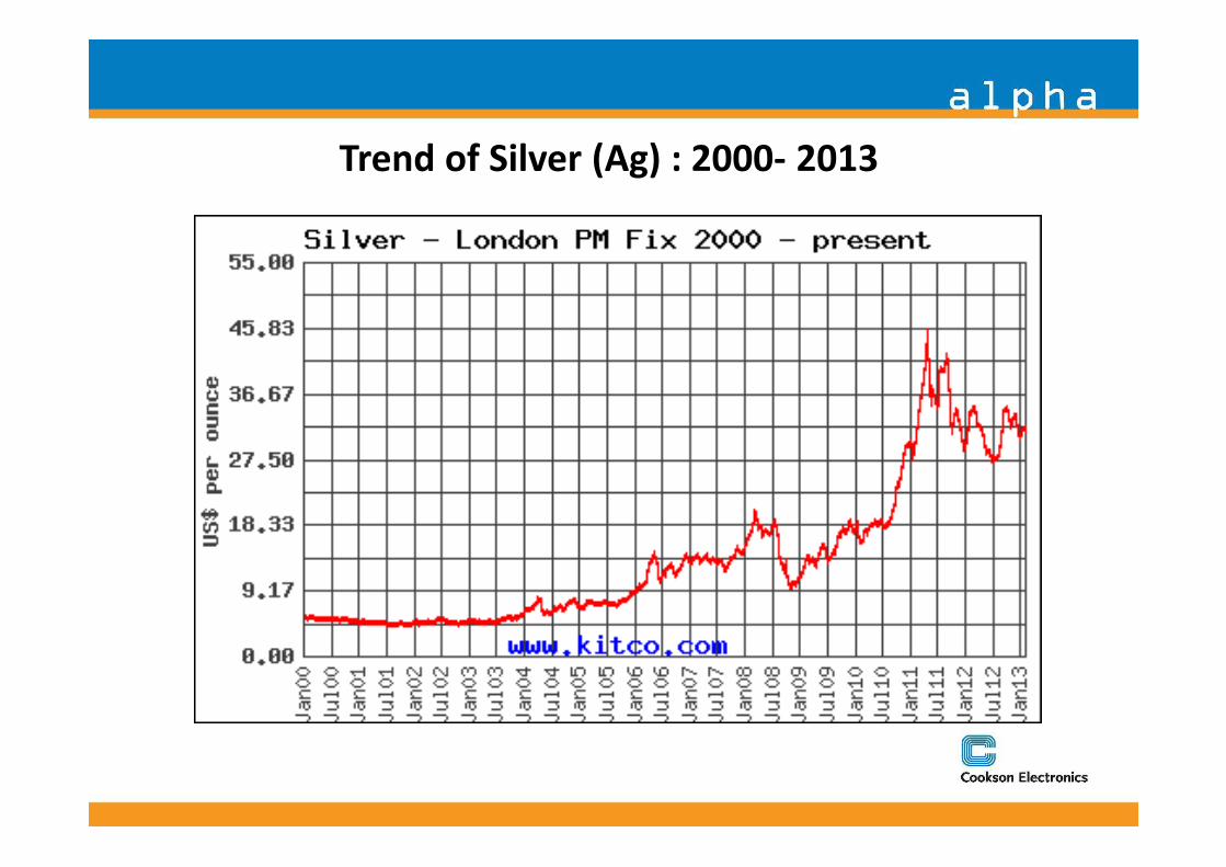
Trend of Silver (Ag) : 2000- 2013
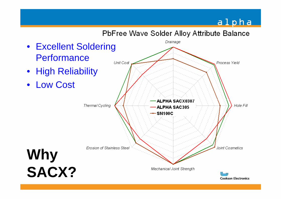
• Excellent Soldering Performance
• High Reliability• Low Cost
Why SACX?
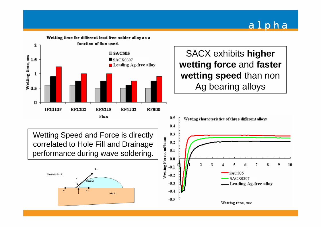
SACX exhibits higher wetting force and faster wetting speed than non
Ag bearing alloys
SACX0307
Wetting Speed and Force is directly correlated to Hole Fill and Drainage performance during wave soldering.
SACX0307
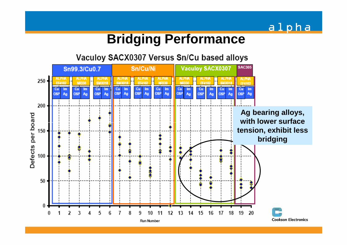
Bridging Performance
Ag bearing alloys, with lower surface Ag bearing alloys, with lower surface with lower surface
tension, exhibit less bridging
with lower surface tension, exhibit less
bridging
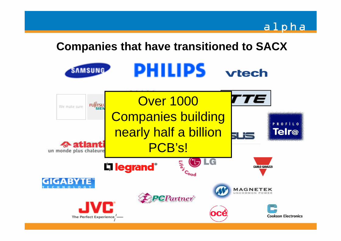
Companies that have transitioned to SACX
Over 1000 Companies building Companies building nearly half a billion
PCB’s!
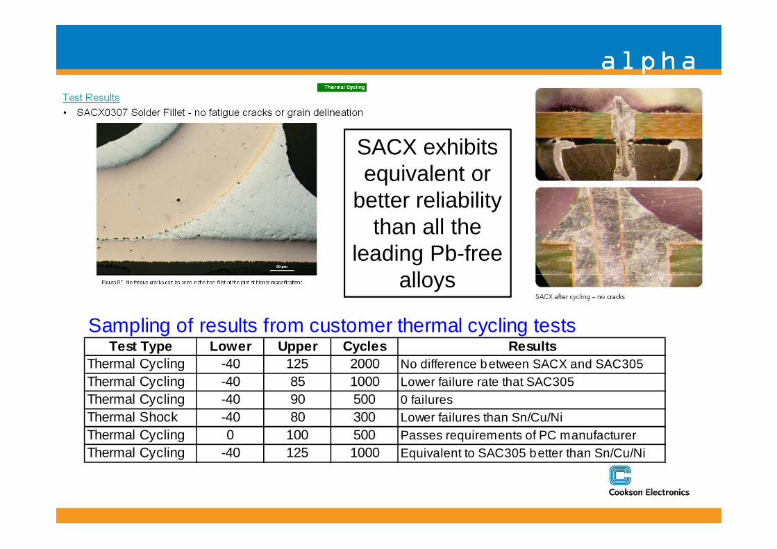
SACX exhibits equivalent or
better reliability than all the
leading Pb-free alloys
Sampling of results from customer thermal cycling testsTest Type Lower Upper Cycles Results
Thermal Cycling -40 125 2000 No difference between SACX and SAC305Thermal Cycling -40 85 1000 Lower failure rate that SAC305Thermal Cycling -40 90 500 0 failuresThermal Shock -40 80 300 Lower failures than Sn/Cu/NiThermal Cycling 0 100 500 Passes requirements of PC manufacturerThermal Cycling -40 125 1000 Equivalent to SAC305 better than Sn/Cu/Ni
alloys
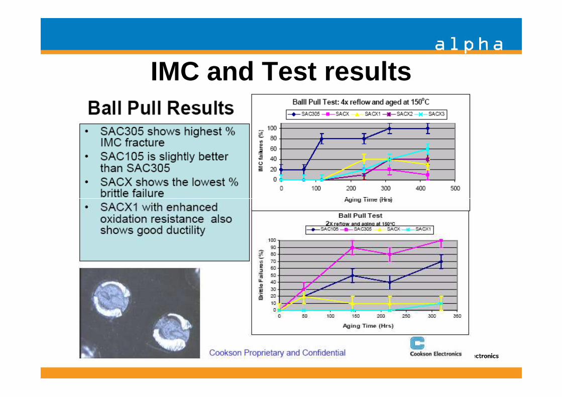
IMC and Test results
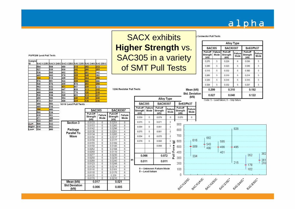
SACX exhibits Higher Strength vs. SAC305 in a variety of SMT Pull Tests
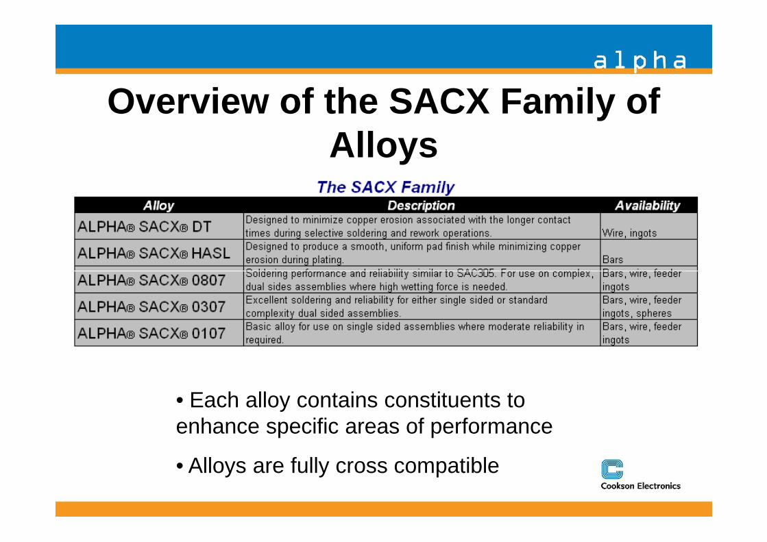
Overview of the SACX Family of Alloys
• Each alloy contains constituents to enhance specific areas of performance
• Alloys are fully cross compatible
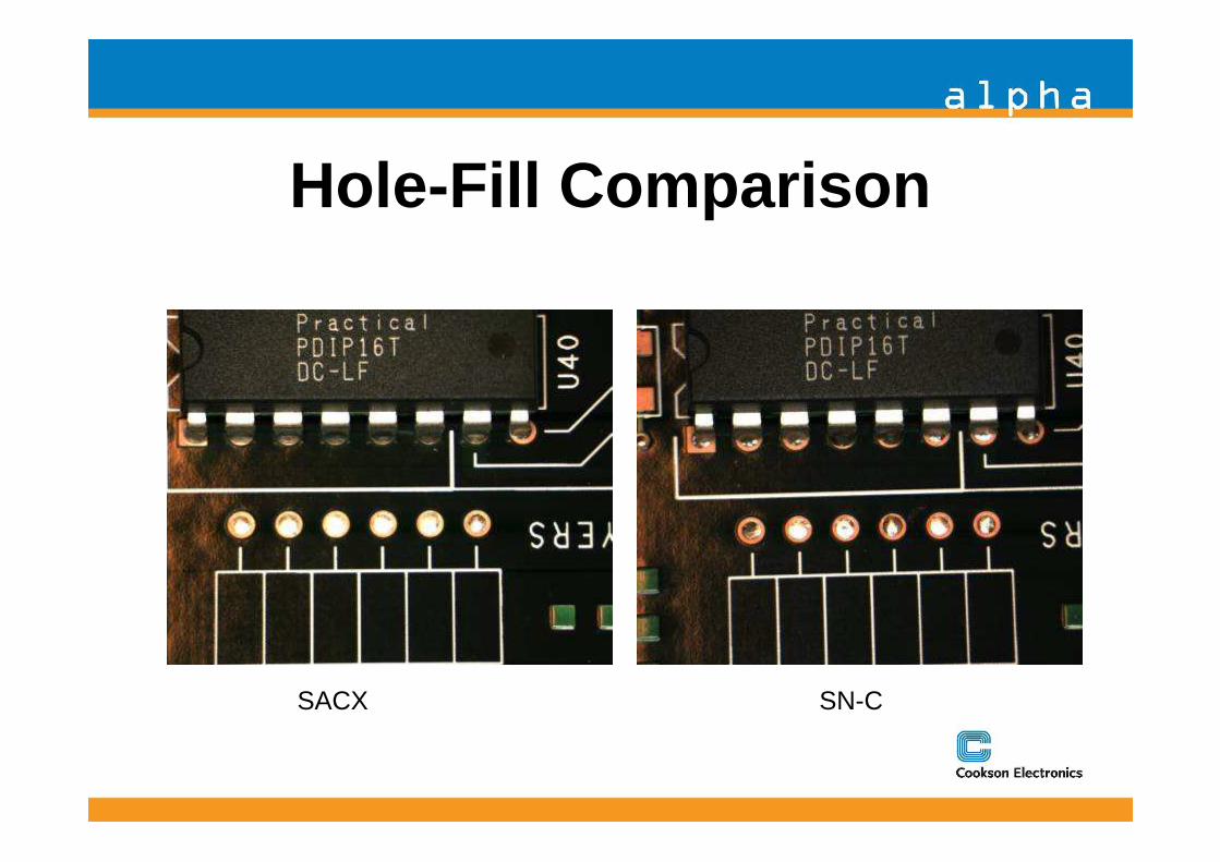
Hole-Fill Comparison
SACX SN-C
Introduction
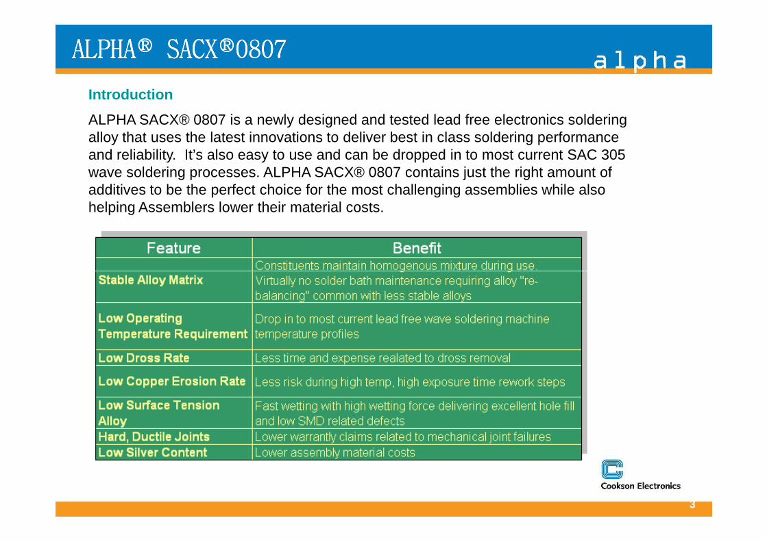
ALPHA SACX® 0807 is a newly designed and tested lead free electronics soldering alloy that uses the latest innovations to deliver best in class soldering performance and reliability. It’s also easy to use and can be dropped in to most current SAC 305 wave soldering processes. ALPHA SACX® 0807 contains just the right amount of additives to be the perfect choice for the most challenging assemblies while also helping Assemblers lower their material costs.
ALPHAALPHAALPHAALPHA®®®® SACXSACXSACXSACX®®®®0807080708070807
3
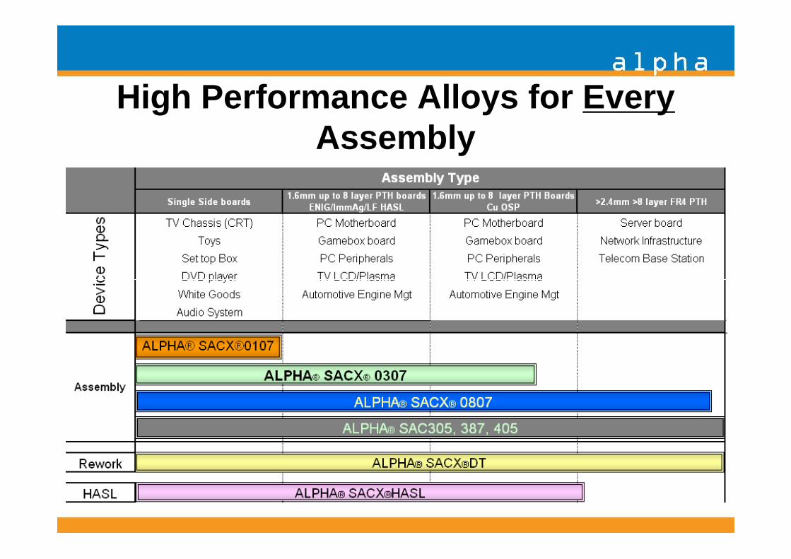
High Performance Alloys for EveryAssembly
Evaluation
of
Paste CVP390-SACX0807
in
A Major EMS in Western region
79
Rajeshwar Andurekar
CTS Engineer – West India
A Major EMS in Western region
20 July 2011.
Background
Presently xxxxx a major EMS player in India is using Alpha OM-345 SAC305 RoHS
( 96.5% Sn, 3.0% Ag, 0.5% Cu) Composition for their OEM customers from
Automotive, Industrial, Telecom & Consumer Electronics Industry segments
The average consumption per month is 850 kg solder paste / month
Continuous pressure from their OEMs to reduce BOM cost was mounting
A meeting was organized for all vendors to review pricingA meeting was organized for all vendors to review pricing
Cookson ( Alpha) proposed the availability of alternate low silver containing
solders like SACX0807, SACX037 & SACX0107 alloys in Solder Paste, Solder Bar &
wire.
So Cookson & the EMS company decided to promote Alpha CVP390-SACX0807
by conducting evaluation and measure the impact on quality
SACX0807 Solder Paste Trials
• Trials were conducted for small & large batch sizes ranging from 10k
to 50K PCBs
• Boards were sent for reliability testing and the data was compared Vs
SAC 305 older paste alloySAC 305 older paste alloy
• A comprehensive report on reliability of solder joints was prepared
and reviewed
• The results exceeded their expectation
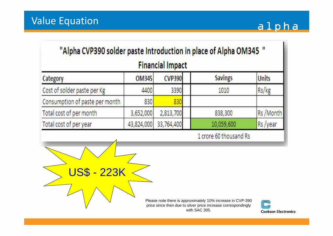
Value Equation
US$ - 223K
Please note there is approximately 10% increase in CVP-390 price since then due to silver price increase correspondingly
with SAC 305.
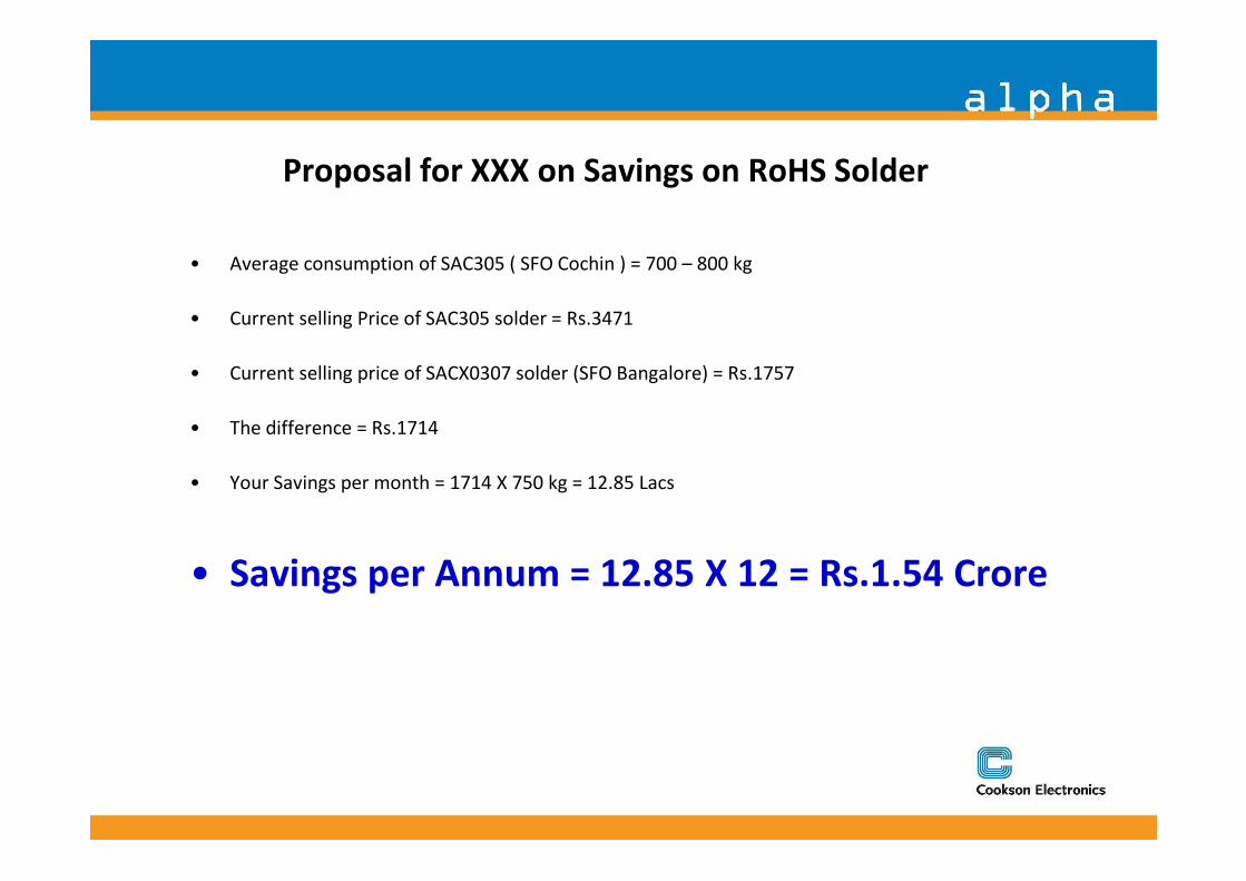
Proposal for XXX on Savings on RoHS Solder
• Average consumption of SAC305 ( SFO Cochin ) = 700 – 800 kg
• Current selling Price of SAC305 solder = Rs.3471
• Current selling price of SACX0307 solder (SFO Bangalore) = Rs.1757
• The difference = Rs.1714
• Your Savings per month = 1714 X 750 kg = 12.85 Lacs
• Savings per Annum = 12.85 X 12 = Rs.1.54 Crore
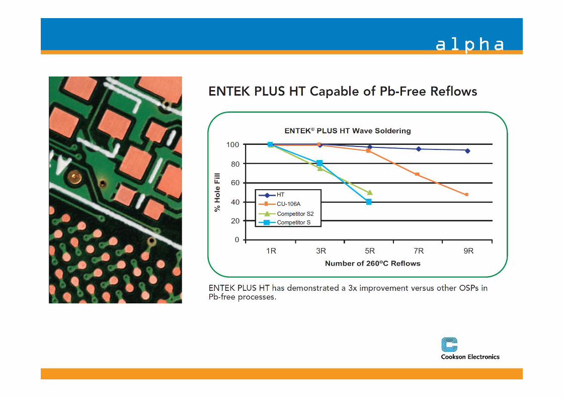
• The actual and projected data in terms of substrate area processed clearly shows a significant bias towards OSP. That does not mean that OSP should be used as a universal finish. Far from the truth.
• What this does mean is that there are a significant number of PCBs assembled today with OSP as its final finish of choice. This includes networking, computer mother boards, automotive electronics including engine control and disk brake systems, mobile phones and other handheld devices. So, contrary to sentiment in some circles, OSPs are not just for low-end consumer electronics. But, again, there other handheld devices. So, contrary to sentiment in some circles, OSPs are not just for low-end consumer electronics. But, again, there are no free lunches. As with any surface finish, there will always be limitations.
So it is appropriate to clearly frame up what the PCB fabricator must do to insure a high-quality and solderable PCB for lead-free assembly when using OSP
The surface finish you select will have a large influence on quality, reliability
and cost.
It is a complex decision that impacts many areas of the business.
Select a finish that optimal for the business (and not just one function).
Summary
Know that there are engineering tricks to improve on weak areas of each
finish.
Stay current in this field because new developments continue to be made.
� Cisco Systems, Inc.
� Multek
� SMT Magazine
� “A Study of Lead-Free Hot Air Leveling”, David Suraski, Circuits Assembly OCT 2004
� “Effects of Surface Finish on High Frequency Signal Loss using Various Substrate
� Materials”, Don Cullen, Bruce Kline, Gary Moderhock, Larry Gatewood - (*1)
� Atotech
� Florida CirTech, Inc.
� Nihon Superior Co., LTD (Osaka, Japan) SN100CL
� Iowa State University
� Senju/Matsushita
� Metal Finishing Industry
� NEMI
Acknowledgements / Credits
� NEMI
� CREEP CORROSION ON LEAD-FREE PRINTED CIRCUIT BOARDS IN HIGH SULFUR ENVIRONMENTS
Randy Schueller, Ph.D.; Dell Inc., Austin, Texas, [email protected]
Randy Schueller, Ph.D., DfR Solutions
� CEMCO – FSL “The Newest Surface Finish Alternative
� LEAD-FREE HASL. It’s Development and Advantages”
� Circuit Connection Presentation (Florida CirTech, Inc. Dec-05-05)
� Chris Padilla (Cisco Systems, Inc.)
� Freeman 1995
� Special Thanks to the following individuals that have contributed to the slides and
animation in this presentation:
Dan Slocum, Craig Davidson, Brad Hammack, Mike Barbetta, Kim Hyland, Glenn Sikorcin