PCB Investigator Documentation · 2018-03-29 · Export a CATIA script Export data to SolidWorks...
57
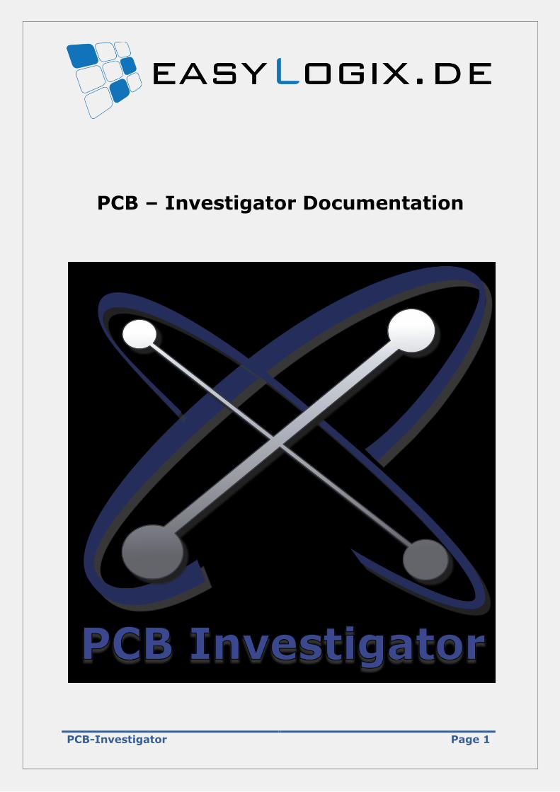
PCB-Investigator Page 1 PCB – Investigator Documentation
Transcript of PCB Investigator Documentation · 2018-03-29 · Export a CATIA script Export data to SolidWorks...
PCB-Investigator Page 1
PCB – Investigator Documentation
PCB-Investigator Page 2
Table of contents
1. Introduction ............................................................................................................................ 4
1.1 Formats .................................................................................................................................... 5
1.2 Top Menu ................................................................................................................................ 5
1.3 PCB - INVESTIGATOR Toolbar .................................................................................................. 6
2. Menus ........................................................................................................................................ 7
2.1 File Menu ................................................................................................................................. 7
2.2 Edit Menu ................................................................................................................................ 7
2.3 View Menu .............................................................................................................................. 8
2.4 Selection Menu ........................................................................................................................ 8
2.5 Extras Menu............................................................................................................................. 9
2.6 Components Menu .................................................................................................................. 9
2.7 Window Menu ....................................................................................................................... 10
2.8 Help Menu ............................................................................................................................. 10
2.9 Export Menu .......................................................................................................................... 10
2.10 Context Menu ........................................................................................................................ 11
3. Functions ................................................................................................................................ 12
3.1 Opening a job ........................................................................................................................ 12
3.2 View Data .............................................................................................................................. 13
3.3 Move and Rotate Objects ...................................................................................................... 16
3.4 Edit Objects ........................................................................................................................... 16
3.5 Compare Layers ..................................................................................................................... 17
3.6 Show and Edit Matrix ............................................................................................................ 18
3.7 Add Bitmap Data ................................................................................................................... 19
3.8 Transform Image Layer .......................................................................................................... 19
3.9 View Component Manager ................................................................................................... 20
3.10 Add ODB++ data .................................................................................................................... 20
3.11 Add Gerber274x, Excellon and Sieb & Meyer data ............................................................... 21
3.12 Find ........................................................................................................................................ 22
PCB-Investigator Page 3
3.13 Strokes ................................................................................................................................... 23
4. Terms and definitions........................................................................................................ 24
4.1 ODB++ .................................................................................................................................... 24
4.2 Gerber274x ............................................................................................................................ 24
4.3 Excellon.................................................................................................................................. 24
4.4 DXF......................................................................................................................................... 24
4.5 Sieb & Meyer ......................................................................................................................... 24
4.6 IPC356 .................................................................................................................................... 24
5. Shortcuts ................................................................................................................................ 25
6. Plug-Ins .................................................................................................................................. 27
6.1 Component Analysis ............................................................................................................. 27
6.2 Bare Board Analysis ............................................................................................................. 30
6.3 Hazard Analysis ................................................................................................................. 32
6.4 Graphic Board Compare ........................................................................................................ 33
6.5 Tombstone Analysis ........................................................................................................... 36
6.6 Database Compare ............................................................................................................... 38
6.7 DFX-Import ............................................................................................................................ 41
6.8 GenCad ............................................................................................................................... 41
6.9 Design Report ....................................................................................................................... 42
6.10 Testpoint Report .................................................................................................................. 43
6.11 Panel Builder ......................................................................................................................... 44
6.12 AOI Import/Export ................................................................................................................ 45
6.13 Net List ................................................................................................................................. 46
6.14 Net Length ............................................................................................................................ 47
6.15 Color Group .......................................................................................................................... 48
6.16 PDF Sync ............................................................................................................................... 50
6.17 Embedded ............................................................................................................................ 52
6.18 IPC 2589 ................................................................................................................................. 52
6.19 Short Cut Top/Buttom View .................................................................................................. 52
6.20 3D Export .............................................................................................................................. 54
6.20.1. Catia Export ....................................................................................................................... 54
6.20.2. SolidWorks Export ............................................................................................................. 56
PCB-Investigator Page 4
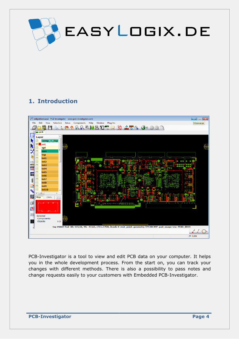
1. Introduction
PCB-Investigator is a tool to view and edit PCB data on your computer. It helps
you in the whole development process. From the start on, you can track your
changes with different methods. There is also a possibility to pass notes and
change requests easily to your customers with Embedded PCB-Investigator.
PCB-Investigator Page 5
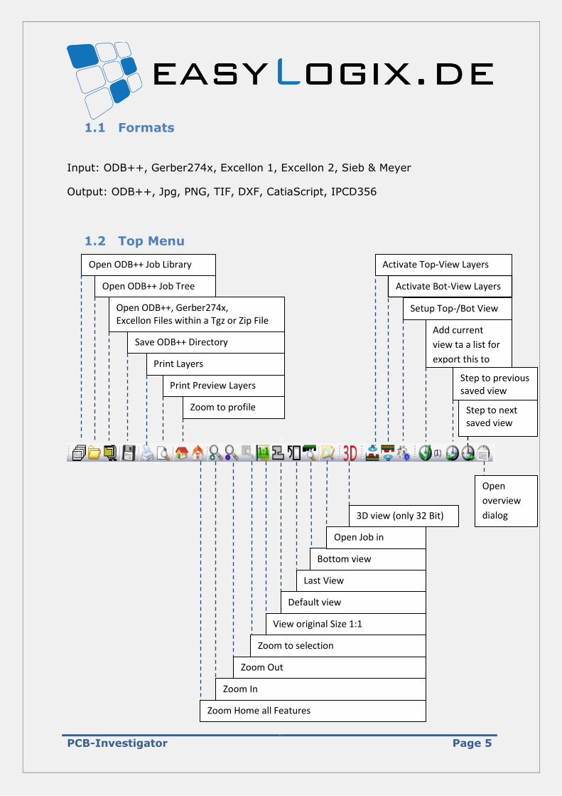
1.1 Formats
Input: ODB++, Gerber274x, Excellon 1, Excellon 2, Sieb & Meyer
Output: ODB++, Jpg, PNG, TIF, DXF, CatiaScript, IPCD356
1.2 Top Menu
Last View
Default view
View original Size 1:1
Zoom Out
Zoom In
Zoom Home all Features
Zoom to profile
Print Preview Layers
Print Layers
Save ODB++ Directory
Open ODB++, Gerber274x, Excellon Files within a Tgz or Zip File
Open ODB++ Job Tree
Open ODB++ Job Library
Bottom view
Open Job in
Explorer
Zoom to selection
3D view (only 32 Bit)
Activate Top-View Layers
Activate Bot-View Layers
Add current
view ta a list for
export this to
Setup Top-/Bot View
Step to previous saved view
Step to next saved view
Open
overview
dialog
PCB-Investigator Page 6
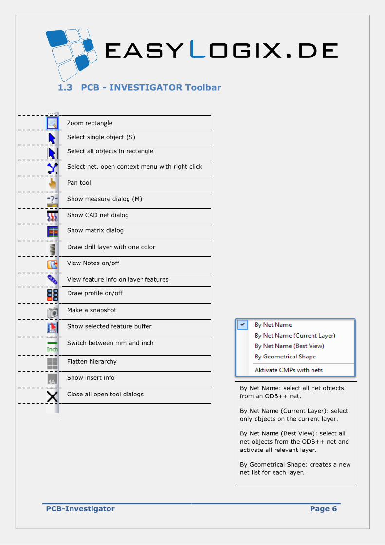
1.3 PCB - INVESTIGATOR Toolbar
By Net Name: select all net objects
from an ODB++ net.
By Net Name (Current Layer): select
only objects on the current layer.
By Net Name (Best View): select all
net objects from the ODB++ net and
activate all relevant layer.
By Geometrical Shape: creates a new
net list for each layer.
Zoom rectangle
Select single object (S)
Select all objects in rectangle
Select net, open context menu with right click
Pan tool
Show measure dialog (M)
Show CAD net dialog
Show matrix dialog
Draw drill layer with one color
View Notes on/off
View feature info on layer features
Draw profile on/off
Make a snapshot
Show selected feature buffer
Switch between mm and inch
Flatten hierarchy
Show insert info
Close all open tool dialogs
PCB-Investigator Page 7
2. Menus
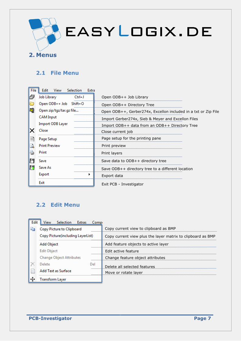
2.1 File Menu
2.2 Edit Menu
Open ODB++ Job Library
Open ODB++ Directory Tree
Open ODB++, Gerber274x, Excellon included in a txt or Zip File
Import Gerber274x, Sieb & Meyer and Excellon Files
Import ODB++ data from an ODB++ Directory Tree
Close current job
Page setup for the printing pane
Print preview
Print layers
Save data to ODB++ directory tree
Exit PCB - Investigator
Save ODB++ directory tree to a different location
Copy current view to clipboard as BMP
Copy current view plus the layer matrix to clipboard as BMP
Add feature objects to active layer
Edit active feature
Change feature object attributes
Delete all selected features
Move or rotate layer
Export data
PCB-Investigator Page 8
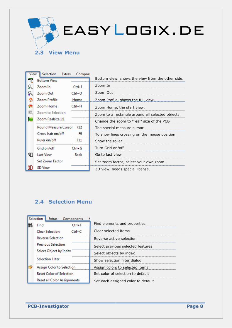
2.3 View Menu
2.4 Selection Menu
Clear selected items
Reverse active selection
Select previous selected features
Show selection filter dialog
Find elements and properties
Select objects by index
Assign colors to selected items
Set color of selection to default
Set each assigned color to default
Bottom view, shows the view from the other side.
Zoom In
Zoom Out
Zoom Profile, shows the full view.
Zoom Home, the start view.
Zoom to a rectangle around all selected objects.
Change the zoom to “real” size of the PCB
The special measure cursor
To show lines crossing on the mouse position
Show the roller
Turn Grid on/off
Go to last view
Set zoom factor, select your own zoom.
3D view, needs special license.
PCB-Investigator Page 9
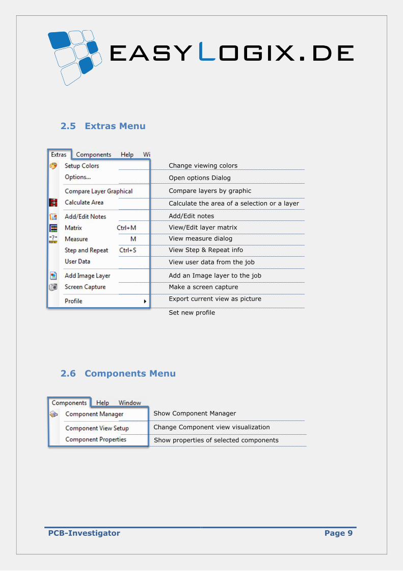
2.5 Extras Menu
2.6 Components Menu
Change viewing colors
Open options Dialog
Compare layers by graphic
Calculate the area of a selection or a layer
Add/Edit notes
View/Edit layer matrix
View measure dialog
View Step & Repeat info
View user data from the job
Add an Image layer to the job
Make a screen capture
Export current view as picture
Set new profile
Show Component Manager
Change Component view visualization
Show properties of selected components
PCB-Investigator Page 10
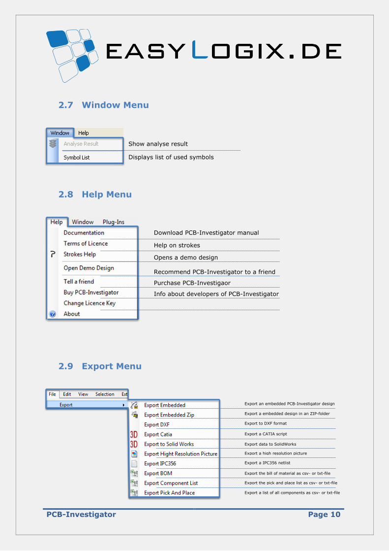
2.7 Window Menu
2.8 Help Menu
2.9 Export Menu
Displays list of used symbols
Show analyse result
Opens a demo design
Help on strokes
Download PCB-Investigator manual
Recommend PCB-Investigator to a friend
Purchase PCB-Investigaor
Info about developers of PCB-Investigator
Export an embedded PCB-Investigator design
Export a embedded design in an ZIP-folder
Export to DXF format
Export a CATIA script
Export data to SolidWorks
Export a high resolution picture
Export a IPC356 netlist
Export the bill of material as csv- or txt-file
Export the pick and place list as csv- or txt-file
Export a list of all components as csv- or txt-file
PCB-Investigator Page 11
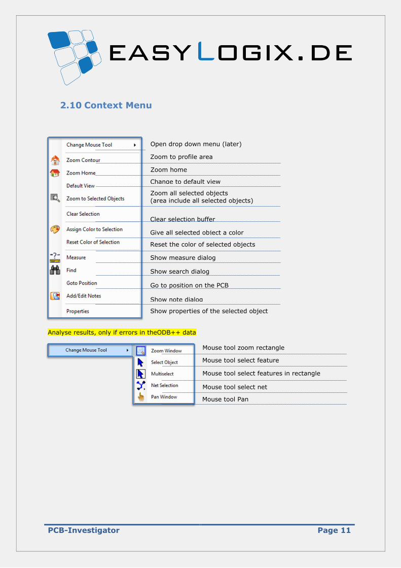
2.10 Context Menu
Analyse results, only if errors in theODB++ data
Open drop down menu (later)
Zoom to profile area
Zoom home
Change to default view
Zoom all selected objects
(area include all selected objects)
Clear selection buffer
Give all selected object a color
Reset the color of selected objects
Show measure dialog
Show search dialog
Go to position on the PCB
Show note dialog
Show properties of the selected object
Mouse tool zoom rectangle
Mouse tool select feature
Mouse tool select features in rectangle
Mouse tool select net
Mouse tool Pan
PCB-Investigator Page 12
3. Functions
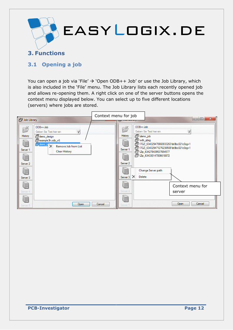
3.1 Opening a job
You can open a job via ‘File’ ‘Open ODB++ Job’ or use the Job Library, which
is also included in the ‘File’ menu. The Job Library lists each recently opened job
and allows re-opening them. A right click on one of the server buttons opens the
context menu displayed below. You can select up to five different locations
(servers) where jobs are stored.
Context menu for job
list
Context menu for
server
PCB-Investigator Page 13
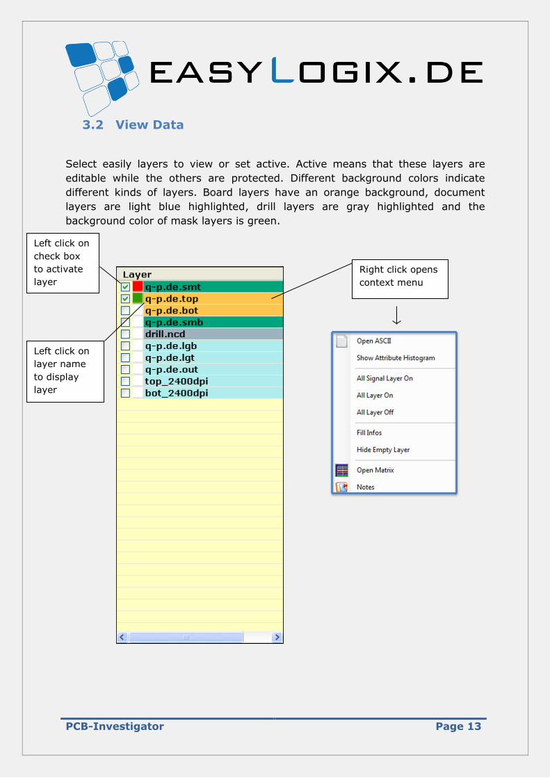
3.2 View Data
Select easily layers to view or set active. Active means that these layers are
editable while the others are protected. Different background colors indicate
different kinds of layers. Board layers have an orange background, document
layers are light blue highlighted, drill layers are gray highlighted and the
background color of mask layers is green.
Left click on
layer name
to display
layer
Left click on
check box
to activate
layer
Right click opens
context menu
PCB-Investigator Page 14
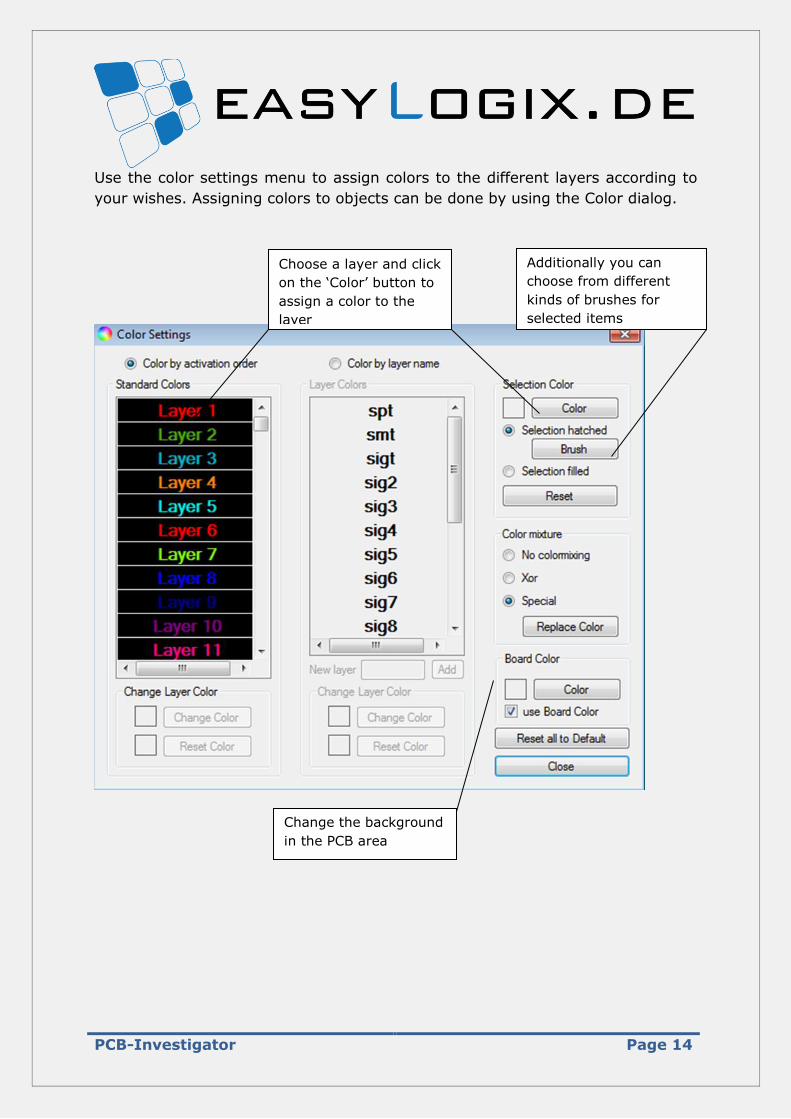
Use the color settings menu to assign colors to the different layers according to
your wishes. Assigning colors to objects can be done by using the Color dialog.
Choose a layer and click
on the ‘Color’ button to
assign a color to the
layer
Additionally you can
choose from different
kinds of brushes for
selected items
Change the background
in the PCB area
PCB-Investigator Page 15
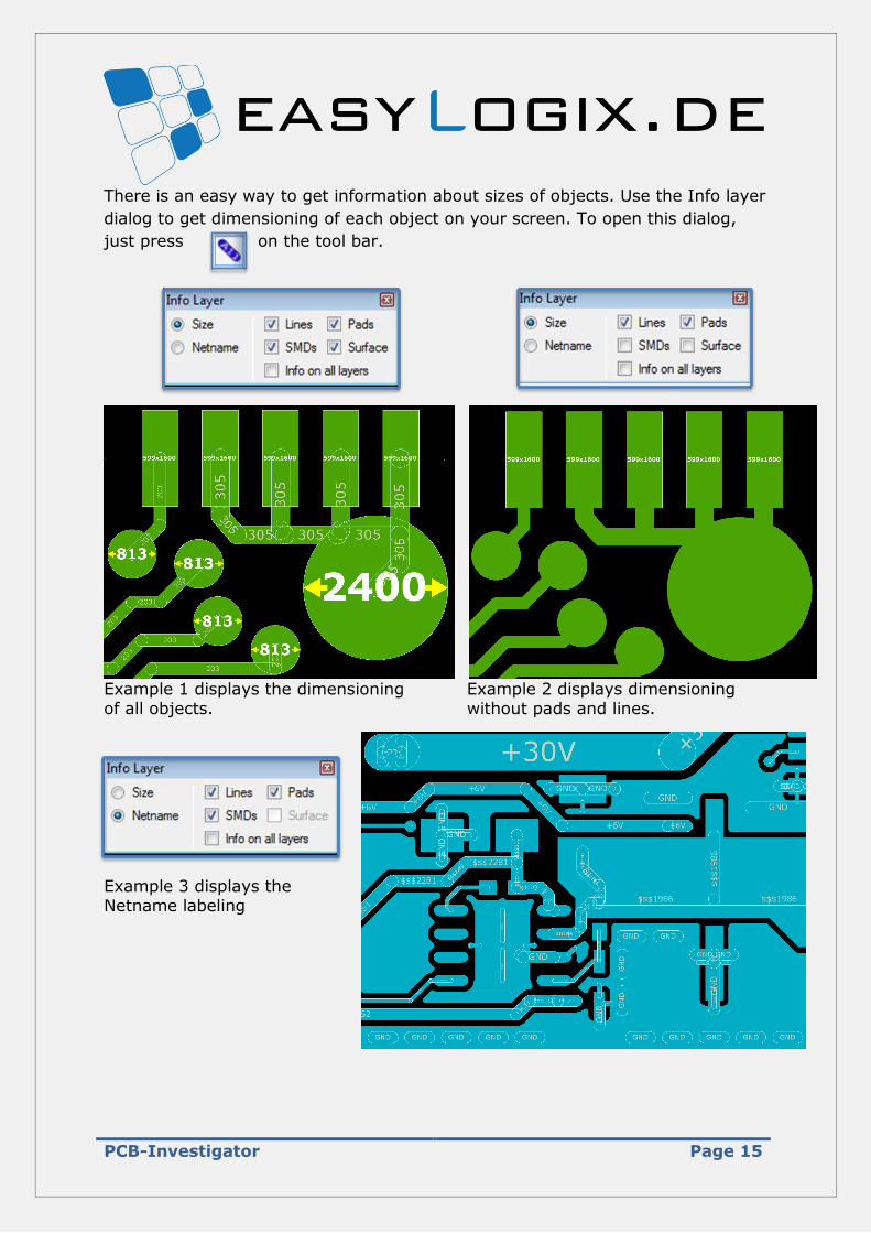
There is an easy way to get information about sizes of objects. Use the Info layer
dialog to get dimensioning of each object on your screen. To open this dialog,
just press on the tool bar.
Example 1 displays the dimensioning Example 2 displays dimensioning of all objects. without pads and lines.
Example 3 displays the Netname labeling
PCB-Investigator Page 16
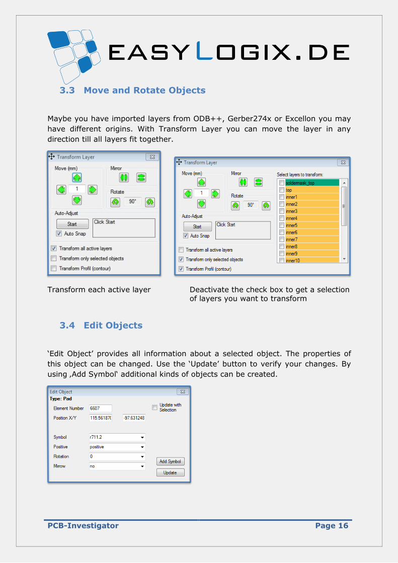
3.3 Move and Rotate Objects
Maybe you have imported layers from ODB++, Gerber274x or Excellon you may
have different origins. With Transform Layer you can move the layer in any
direction till all layers fit together.
Transform each active layer Deactivate the check box to get a selection of layers you want to transform
3.4 Edit Objects
‘Edit Object’ provides all information about a selected object. The properties of
this object can be changed. Use the ‘Update’ button to verify your changes. By
using ‚Add Symbol‘ additional kinds of objects can be created.
PCB-Investigator Page 17
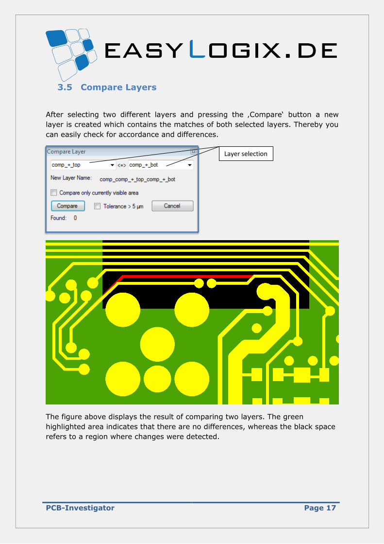
3.5 Compare Layers
After selecting two different layers and pressing the ‚Compare‘ button a new
layer is created which contains the matches of both selected layers. Thereby you
can easily check for accordance and differences.
The figure above displays the result of comparing two layers. The green
highlighted area indicates that there are no differences, whereas the black space
refers to a region where changes were detected.
Layer selection
PCB-Investigator Page 18
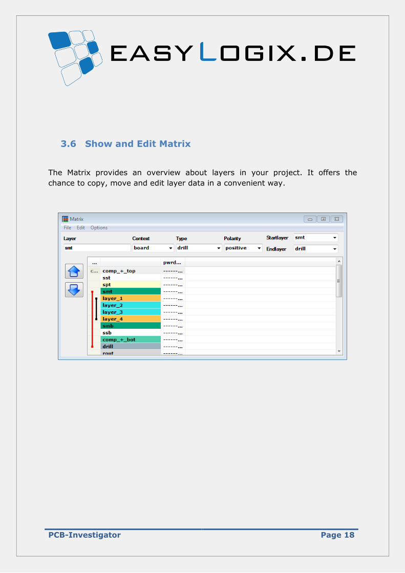
3.6 Show and Edit Matrix
The Matrix provides an overview about layers in your project. It offers the
chance to copy, move and edit layer data in a convenient way.
PCB-Investigator Page 19
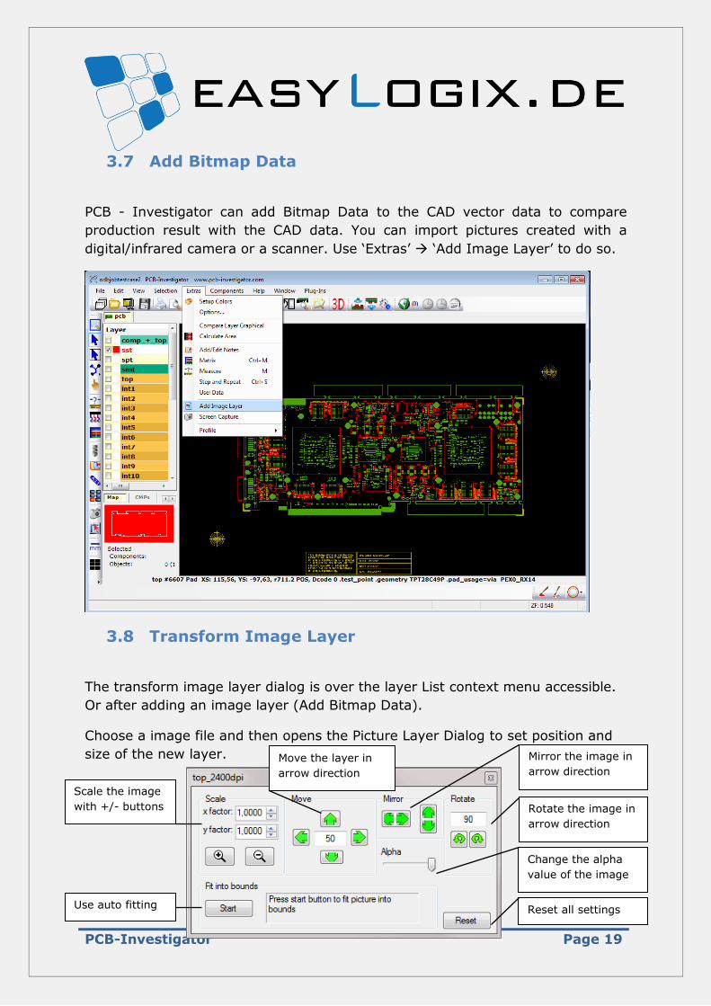
3.7 Add Bitmap Data
PCB - Investigator can add Bitmap Data to the CAD vector data to compare
production result with the CAD data. You can import pictures created with a
digital/infrared camera or a scanner. Use ‘Extras’ ‘Add Image Layer’ to do so.
3.8 Transform Image Layer
The transform image layer dialog is over the layer List context menu accessible.
Or after adding an image layer (Add Bitmap Data).
Choose a image file and then opens the Picture Layer Dialog to set position and
size of the new layer.
Scale the image
with +/- buttons
Mirror the image in
arrow direction
Rotate the image in
arrow direction
Change the alpha
value of the image
Reset all settings Use auto fitting
Move the layer in
arrow direction
PCB-Investigator Page 20
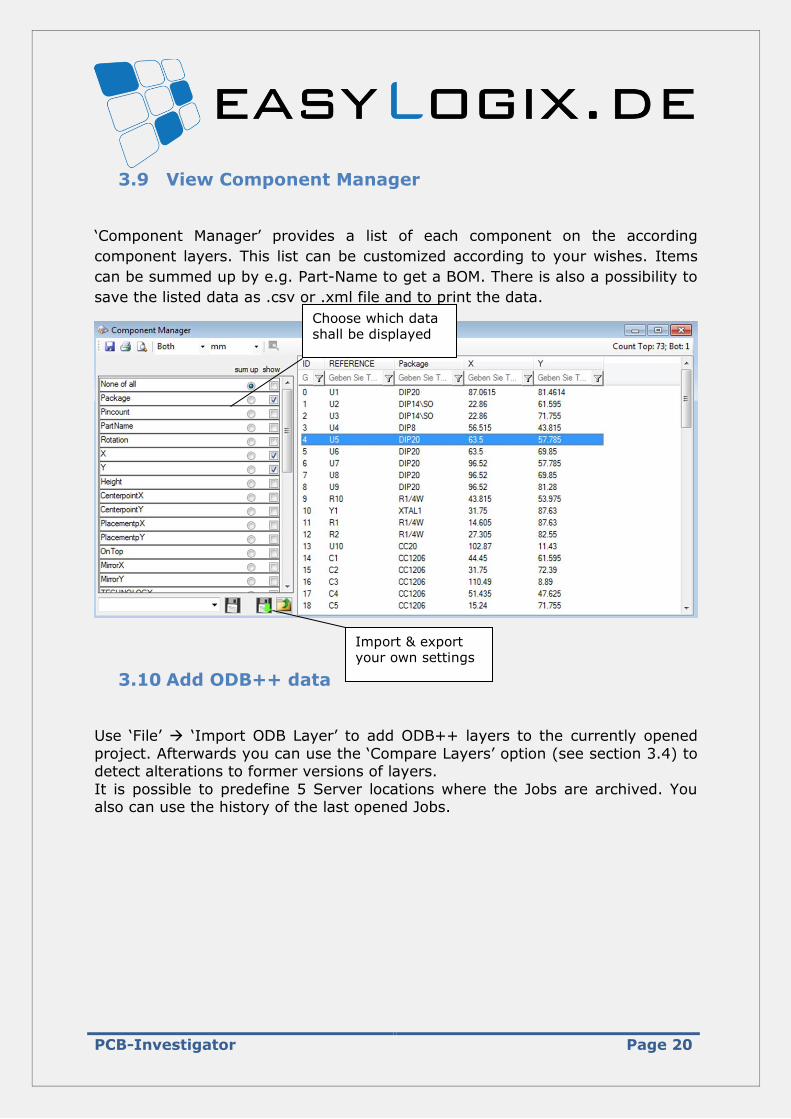
3.9 View Component Manager
‘Component Manager’ provides a list of each component on the according
component layers. This list can be customized according to your wishes. Items
can be summed up by e.g. Part-Name to get a BOM. There is also a possibility to
save the listed data as .csv or .xml file and to print the data.
3.10 Add ODB++ data
Use ‘File’ ‘Import ODB Layer’ to add ODB++ layers to the currently opened
project. Afterwards you can use the ‘Compare Layers’ option (see section 3.4) to detect alterations to former versions of layers.
It is possible to predefine 5 Server locations where the Jobs are archived. You also can use the history of the last opened Jobs.
Choose which data shall be displayed
Import & export your own settings
PCB-Investigator Page 21
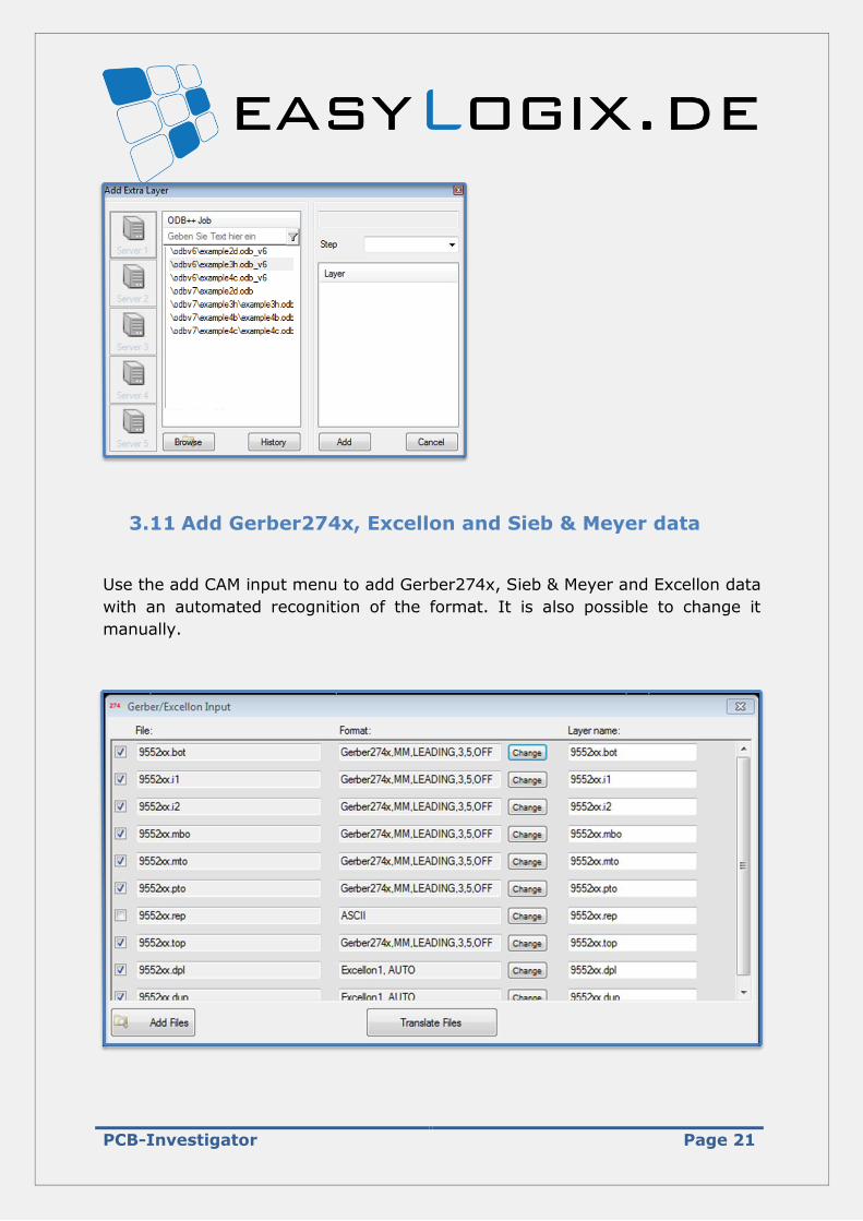
3.11 Add Gerber274x, Excellon and Sieb & Meyer data
Use the add CAM input menu to add Gerber274x, Sieb & Meyer and Excellon data
with an automated recognition of the format. It is also possible to change it
manually.
PCB-Investigator Page 22
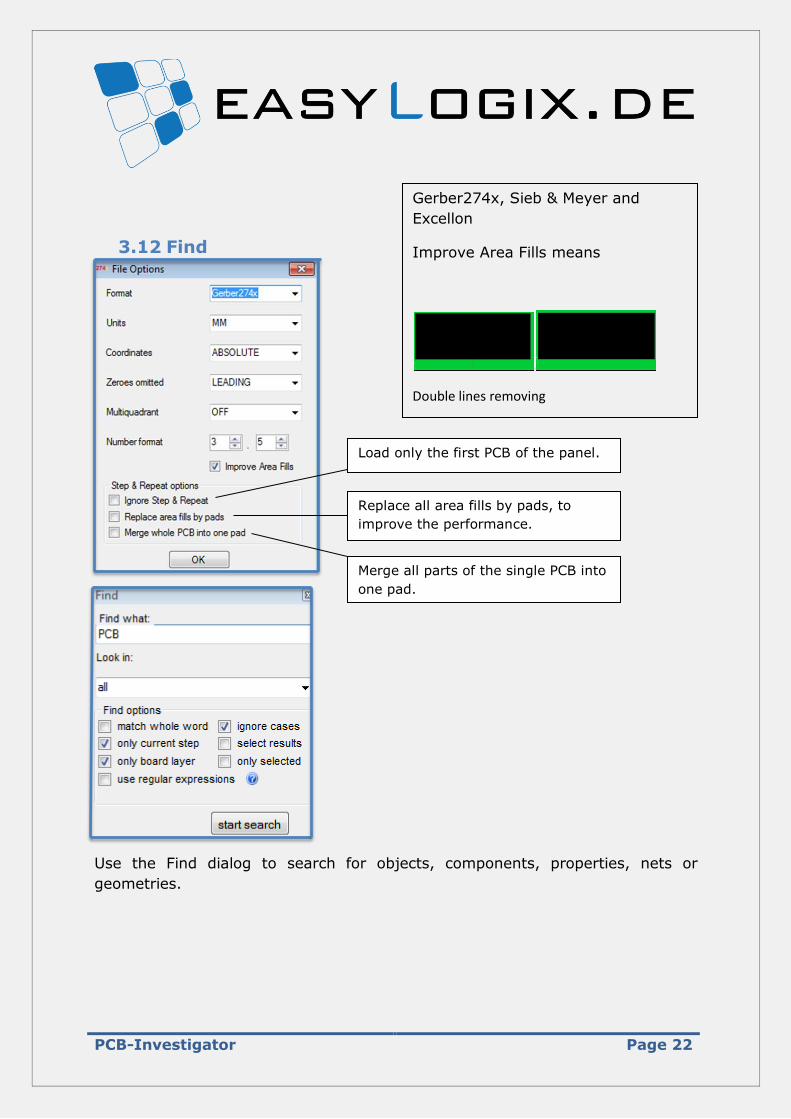
3.12 Find
Use the Find dialog to search for objects, components, properties, nets or
geometries.
Gerber274x, Sieb & Meyer and
Excellon
Improve Area Fills means
Double lines removing
Load only the first PCB of the panel.
Replace all area fills by pads, to
improve the performance.
Merge all parts of the single PCB into
one pad.
PCB-Investigator Page 23
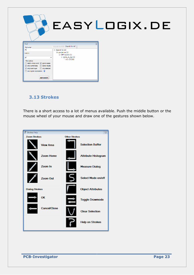
3.13 Strokes
There is a short access to a lot of menus available. Push the middle button or the
mouse wheel of your mouse and draw one of the gestures shown below.
PCB-Investigator Page 24
4. Terms and definitions
4.1 ODB++
All modern layout tools have options to write ODB++. You can use the option
write to directory or the option to write it to .Tgz file. The advantage is to get
detailed information within the job. So it can be used during developing process.
4.2 Gerber274x
Gerber274x is ASCII vector graphic format. This format includes also the
definition of the apertures which will be used for drawing.
4.3 Excellon
Excellon is used for drill data.
4.4 DXF
DXF is a 2D and 3D Data Exchange Format.
4.5 Sieb & Meyer
Sieb & Meyer data is used for describing CNC manufacturing.
4.6 IPC356
A special definition of netlist data.
PCB-Investigator Page 25
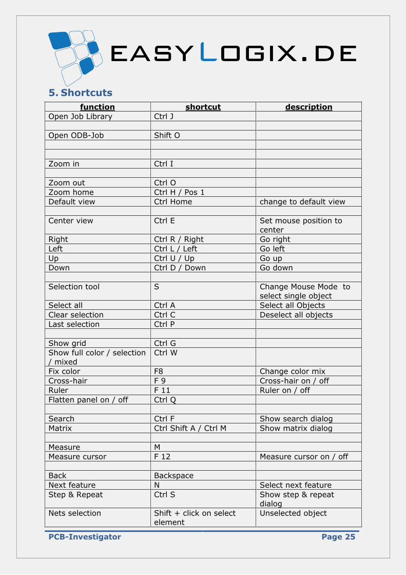
5. Shortcuts
function shortcut description
Open Job Library Ctrl J
Open ODB-Job Shift O
Zoom in Ctrl I
Zoom out Ctrl O
Zoom home Ctrl H / Pos 1
Default view Ctrl Home change to default view
Center view Ctrl E Set mouse position to
center
Right Ctrl R / Right Go right
Left Ctrl L / Left Go left
Up Ctrl U / Up Go up
Down Ctrl D / Down Go down
Selection tool S Change Mouse Mode to
select single object
Select all Ctrl A Select all Objects
Clear selection Ctrl C Deselect all objects
Last selection Ctrl P
Show grid Ctrl G
Show full color / selection
/ mixed
Ctrl W
Fix color F8 Change color mix
Cross-hair F 9 Cross-hair on / off
Ruler F 11 Ruler on / off
Flatten panel on / off Ctrl Q
Search Ctrl F Show search dialog
Matrix Ctrl Shift A / Ctrl M Show matrix dialog
Measure M
Measure cursor F 12 Measure cursor on / off
Back Backspace
Next feature N Select next feature
Step & Repeat Ctrl S Show step & repeat dialog
Nets selection Shift + click on select
element
Unselected object
PCB-Investigator Page 26
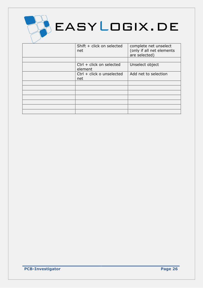
Shift + click on selected net
complete net unselect (only if all net elements are selected)
Ctrl + click on selected element
Unselect object
Ctrl + click o unselected net
Add net to selection
PCB-Investigator Page 27
6. Plug-Ins
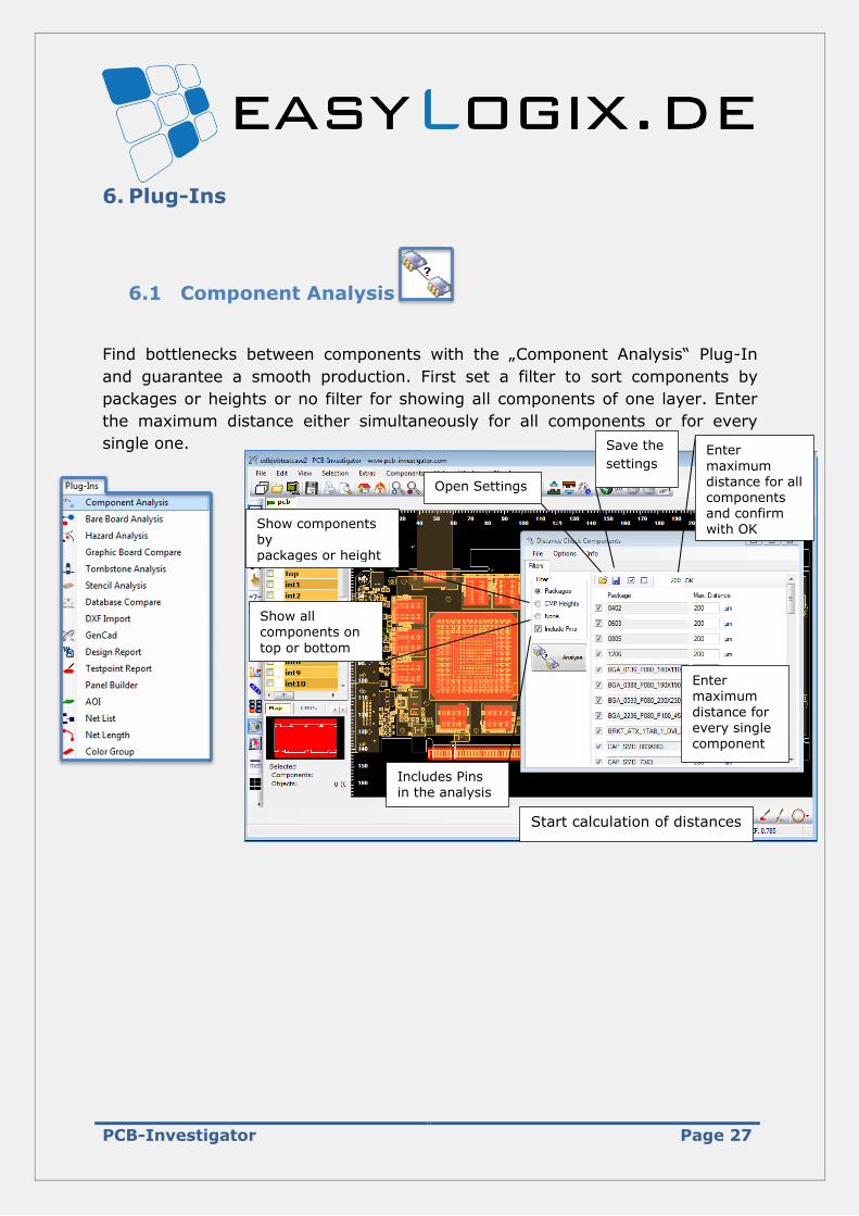
6.1 Component Analysis
Find bottlenecks between components with the „Component Analysis“ Plug-In
and guarantee a smooth production. First set a filter to sort components by
packages or heights or no filter for showing all components of one layer. Enter
the maximum distance either simultaneously for all components or for every
single one.
Start calculation of distances
Show components by packages or height
Show all components on
top or bottom
Includes Pins in the analysis
Open Settings
Save the
settings Enter
maximum distance for all components and confirm with OK
Enter maximum
distance for every single component
PCB-Investigator Page 28
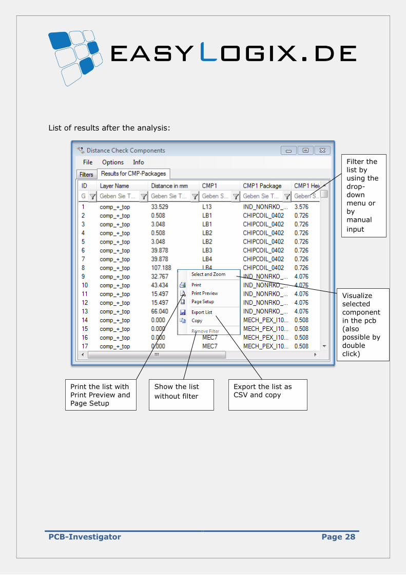
List of results after the analysis:
Filter the
list by
using the
drop-
down
menu or
by
manual
input
Visualize
selected
component
in the pcb
(also
possible by
double
click)
Print the list with
Print Preview and
Page Setup
Export the list as CSV and copy
Show the list
without filter
PCB-Investigator Page 29
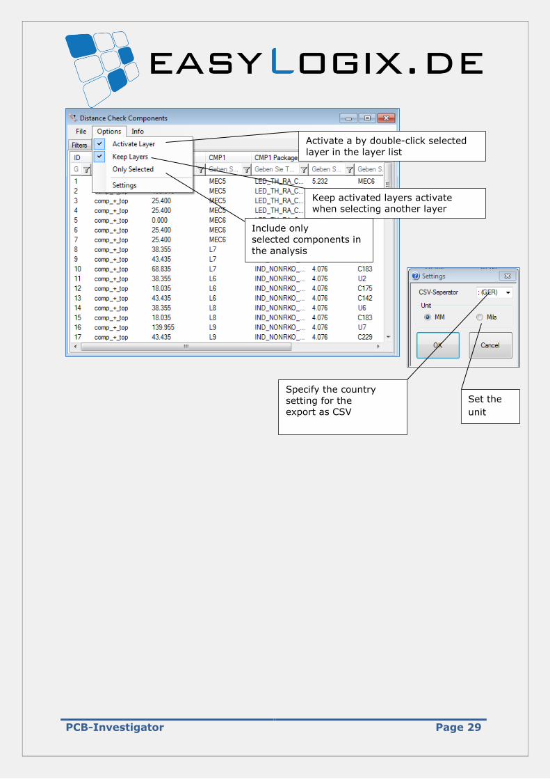
Activate a by double-click selected
layer in the layer list
Keep activated layers activate when selecting another layer
Include only
selected components in
the analysis
Specify the country
setting for the
export as CSV
Set the
unit
PCB-Investigator Page 30
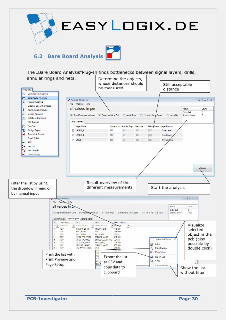
6.2 Bare Board Analysis
The „Bare Board Analysis“Plug-In finds bottlenecks between signal layers, drills,
annular rings and nets.
Determine the objects,
whose distances should
be measured. Still acceptable
distance
Result overview of the
different measurements Start the analysis Filter the list by using the dropdown menu or by manual input
Visualize
selected
object in the
pcb (also
possible by double click)
Show the list
without filter
Export the list as CSV and copy data to clipboard
Print the list with Print Preview and Page Setup
PCB-Investigator Page 31
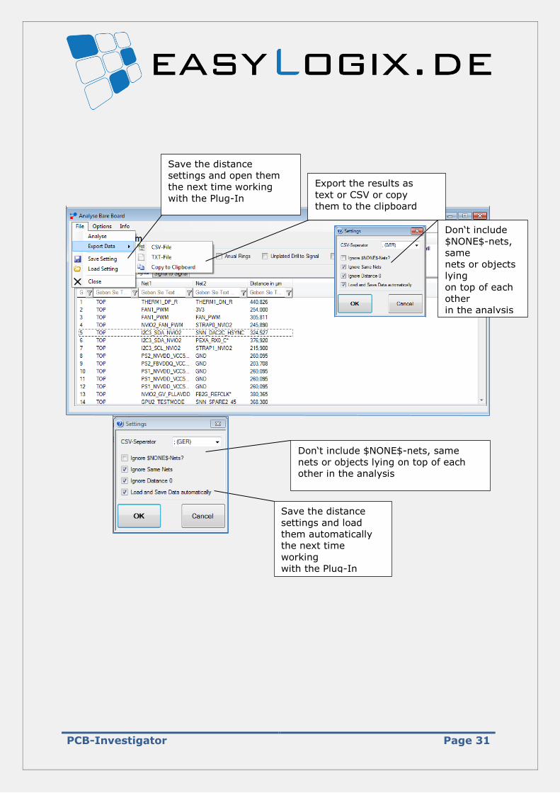
Save the distance
settings and open them
the next time working
with the Plug-In
Export the results as
text or CSV or copy
them to the clipboard
Don‘t include
$NONE$-nets,
same
nets or objects
lying
on top of each
other
in the analysis
Save the distance
settings and load
them automatically
the next time
working
with the Plug-In
Don‘t include $NONE$-nets, same
nets or objects lying on top of each
other in the analysis
PCB-Investigator Page 32
Show components
or objects color marked in the pcb
Copy, export or print the results
See the results
without the filter
6.3 Hazard Analysis
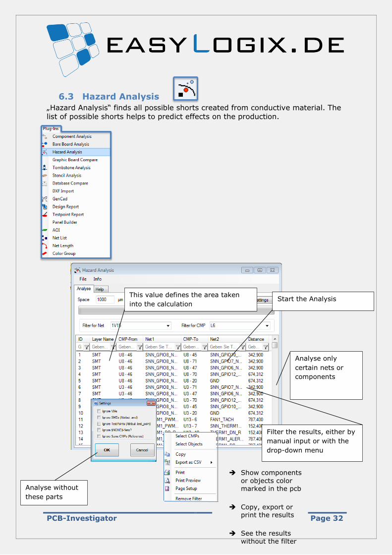
„Hazard Analysis“ finds all possible shorts created from conductive material. The
list of possible shorts helps to predict effects on the production.
This value defines the area taken
into the calculation Start the Analysis
Analyse only
certain nets or
components
Filter the results, either by
manual input or with the
drop-down menu
Analyse without
these parts
PCB-Investigator Page 33
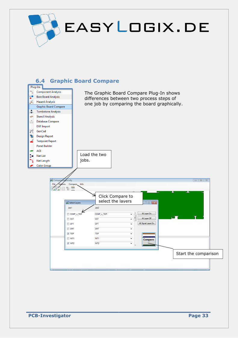
6.4 Graphic Board Compare
Load the two
jobs.
Click Compare to
select the layers
Start the comparison
The Graphic Board Compare Plug-In shows differences between two process steps of
one job by comparing the board graphically.
PCB-Investigator Page 34
The whole board.
List of the clips
that show differences
Click on a
clip in the
list to
see it
zoomed in
in the
left handed
part of the
window and
red marked
on the
whole
board
PCB-Investigator Page 35
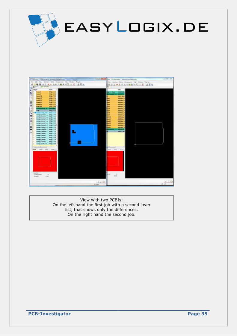
View with two PCBIs:
On the left hand the first job with a second layer
list, that shows only the differences.
On the right hand the second job.
PCB-Investigator Page 36
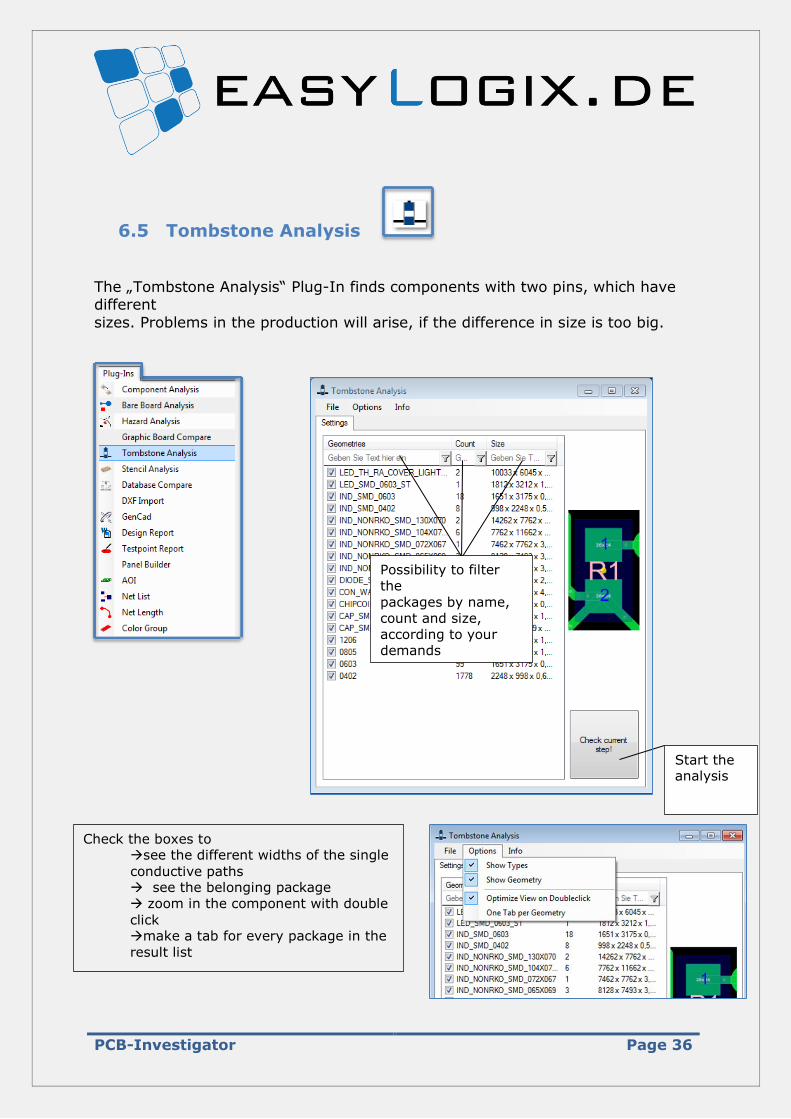
6.5 Tombstone Analysis
The „Tombstone Analysis“ Plug-In finds components with two pins, which have different
sizes. Problems in the production will arise, if the difference in size is too big.
Possibility to filter
the
packages by name,
count and size,
according to your
demands
Start the analysis
Check the boxes to see the different widths of the single
conductive paths see the belonging package
zoom in the component with double
click make a tab for every package in the
result list
PCB-Investigator Page 37
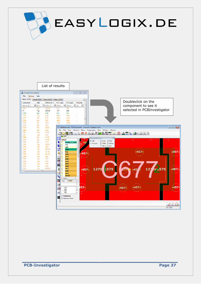
List of results
Doubleclick on the
component to see it
selected in PCBInvestigator
PCB-Investigator Page 38
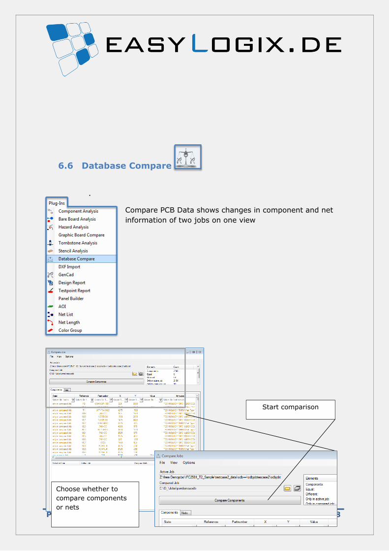
6.6 Database Compare
.
Compare PCB Data shows changes in component and net
information of two jobs on one view
Choose the job to be
compared
to the active job: Either by
Job
Library or by searching on
your computer
Start comparison
Choose whether to
compare components
or nets
PCB-Investigator Page 39
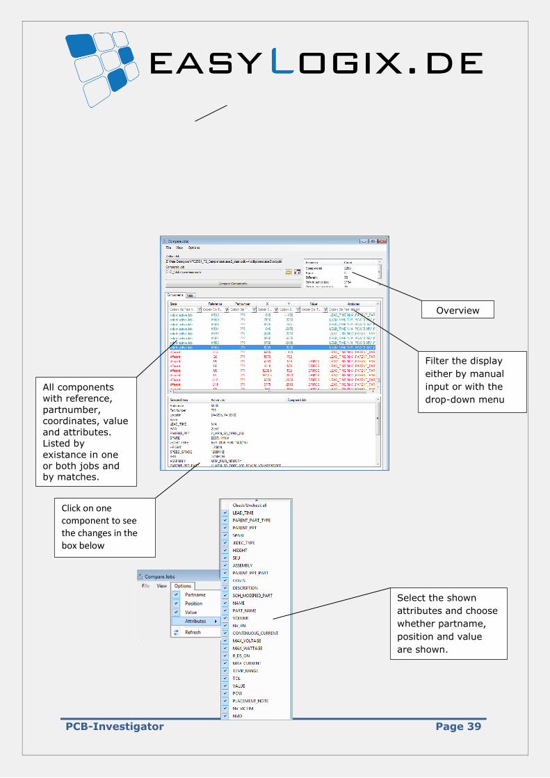
Overview
Filter the display
either by manual
input or with the
drop-down menu
All components
with reference,
partnumber,
coordinates, value
and attributes.
Listed by
existance in one
or both jobs and by matches.
Click on one component to see the changes in the box below
Select the shown
attributes and choose
whether partname,
position and value
are shown.
PCB-Investigator Page 40
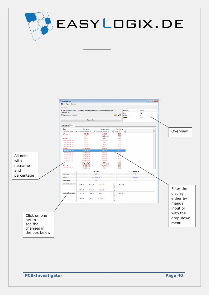
Refresh the
results
All nets
with
netname
and
percentage
of matches
Overview
Filter the
display
either by
manual
input or
with the
drop-down
menu
Click on one
net to
see the
changes in
the box below
PCB-Investigator Page 41
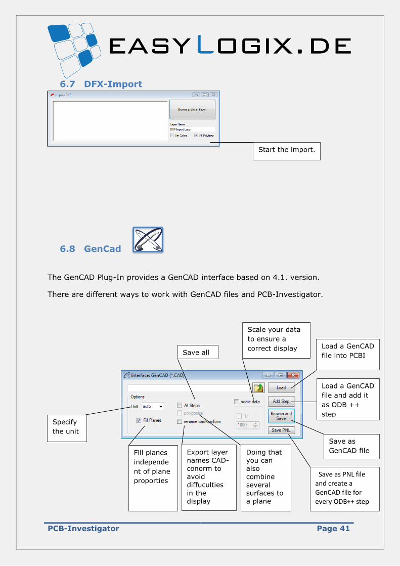
6.7 DFX-Import
6.8 GenCad
The GenCAD Plug-In provides a GenCAD interface based on 4.1. version.
There are different ways to work with GenCAD files and PCB-Investigator.
Save all
steps
Scale your data
to ensure a
correct display Load a GenCAD
file into PCBI
Load a GenCAD
file and add it
as ODB ++
step
Save as
GenCAD file
Save as PNL file and create a GenCAD file for every ODB++ step
Doing that
you can
also
combine
several
surfaces to
a plane
Export layer
names CAD-
conorm to
avoid
diffuculties
in the
display
Fill planes
independe
nt of plane
proporties
Specify
the unit
Start the import.
PCB-Investigator Page 42
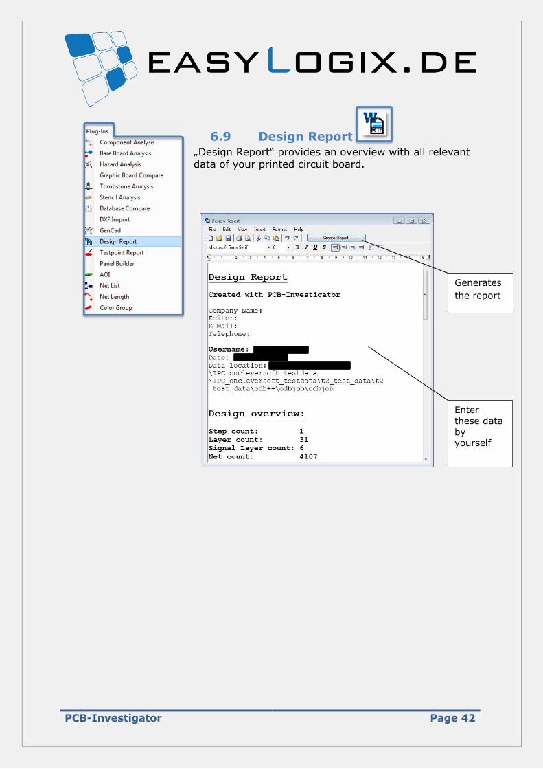
6.9 Design Report
„Design Report“ provides an overview with all relevant
data of your printed circuit board.
Generates
the report
Enter
these data
by yourself
PCB-Investigator Page 43
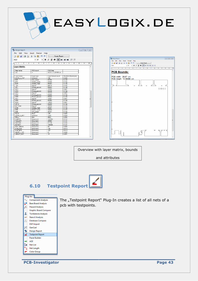
6.10 Testpoint Report
The „Testpoint Report“ Plug-In creates a list of all nets of a
pcb with testpoints.
Overview with layer matrix, bounds
and attributes
PCB-Investigator Page 44
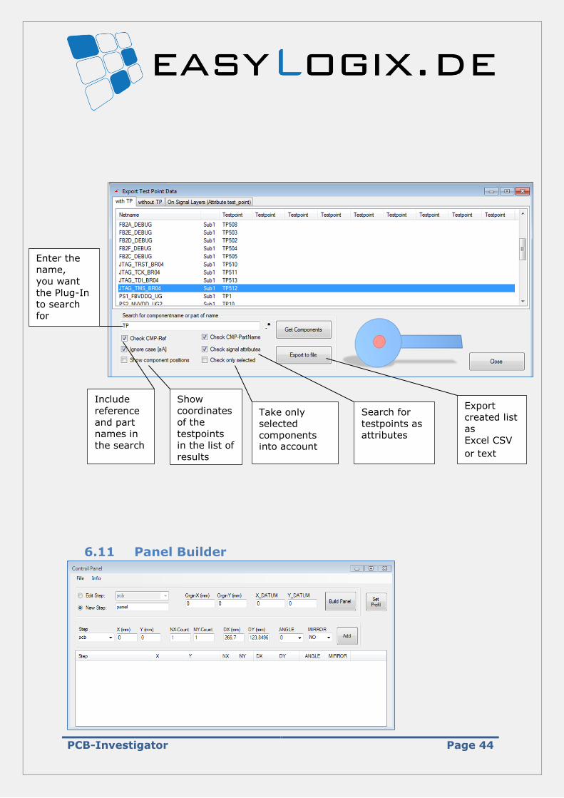
6.11 Panel Builder
Export
created list
as
Excel CSV
or text
Search for
testpoints as attributes
Take only
selected
components into account
Show
coordinates
of the
testpoints
in the list of
results
Include
reference
and part
names in
the search
Enter the
name,
you want
the Plug-In
to search
for
PCB-Investigator Page 45
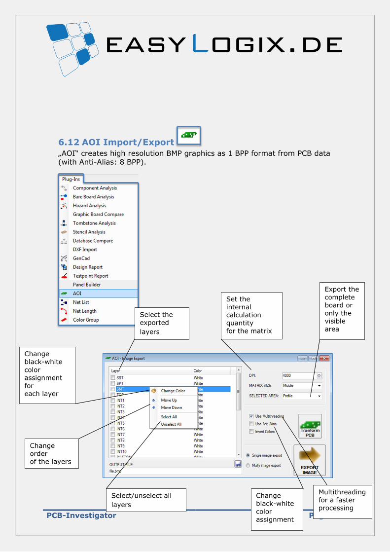
6.12 AOI Import/Export
„AOI“ creates high resolution BMP graphics as 1 BPP format from PCB data (with Anti-Alias: 8 BPP).
Select the
exported
layers
Set the
internal
calculation
quantity
for the matrix
Export the
complete
board or
only the
visible
area
Multithreading
for a faster
processing
Change
black-white
color
assignment
Change
order
of the layers
Change
black-white
color
assignment
for
each layer
Select/unselect all
layers
PCB-Investigator Page 46
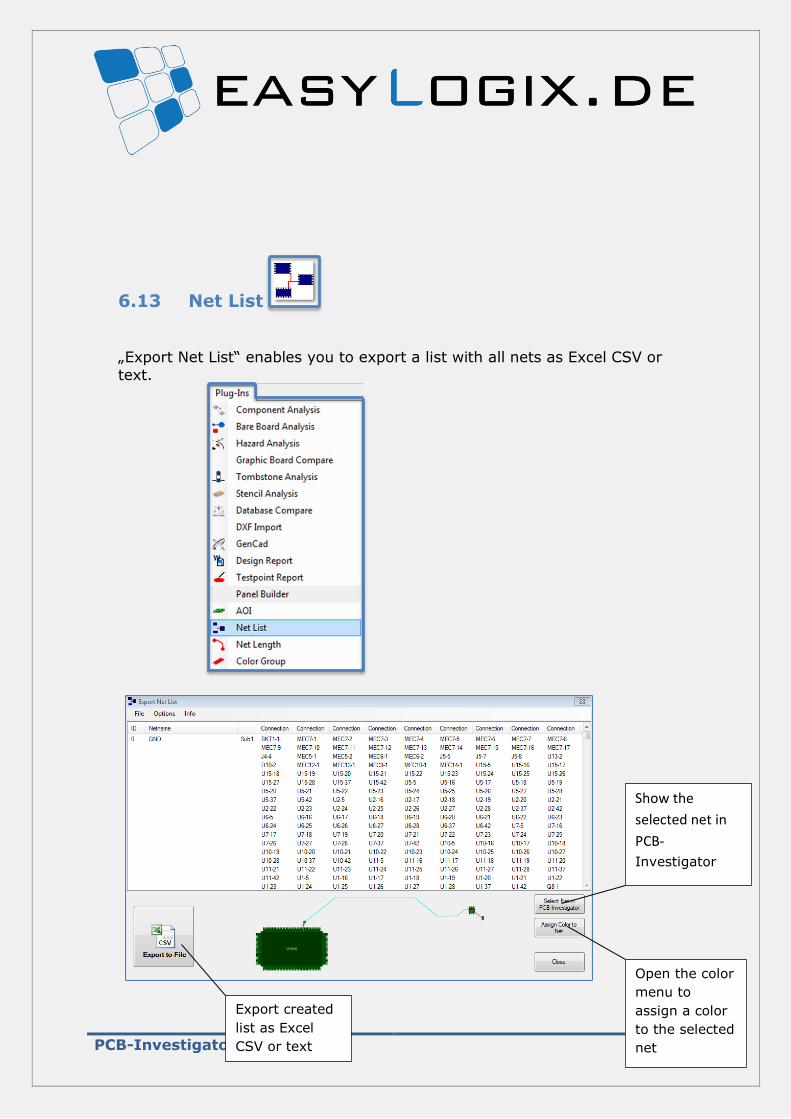
6.13 Net List
„Export Net List“ enables you to export a list with all nets as Excel CSV or
text.
Show the
selected net in
PCB-
Investigator
Open the color
menu to
assign a color
to the selected
net
Export created
list as Excel
CSV or text
PCB-Investigator Page 47
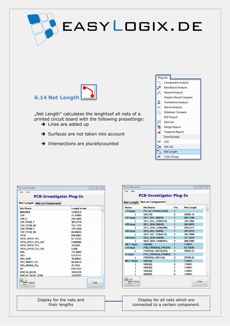
6.14 Net Length
„Net Length” calculates the lenghtsof all nets of a
printed circuit board with the following presettings: Lines are added up
Surfaces are not taken into account
Intersections are plurallycounted
Display for the nets and
their lengths
Display for all nets which are
connected to a certain component.
PCB-Investigator Page 48
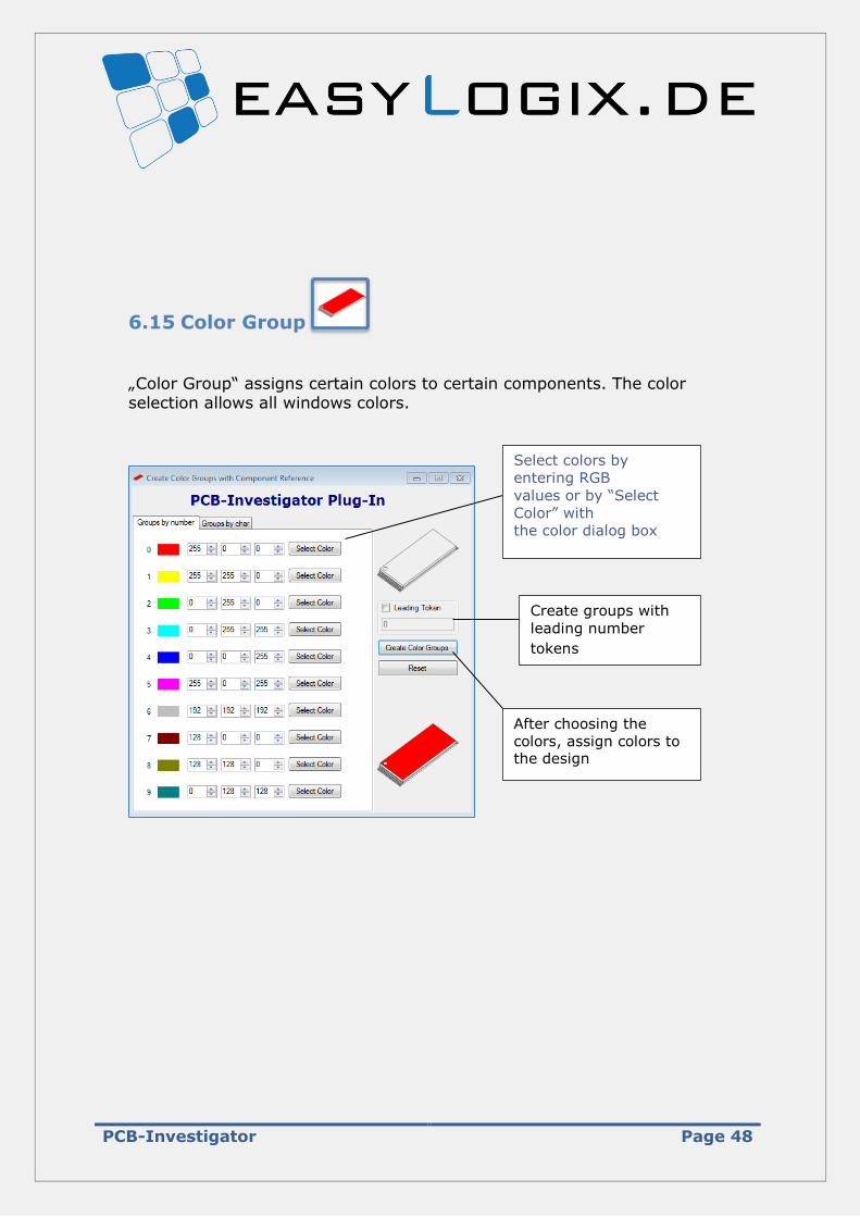
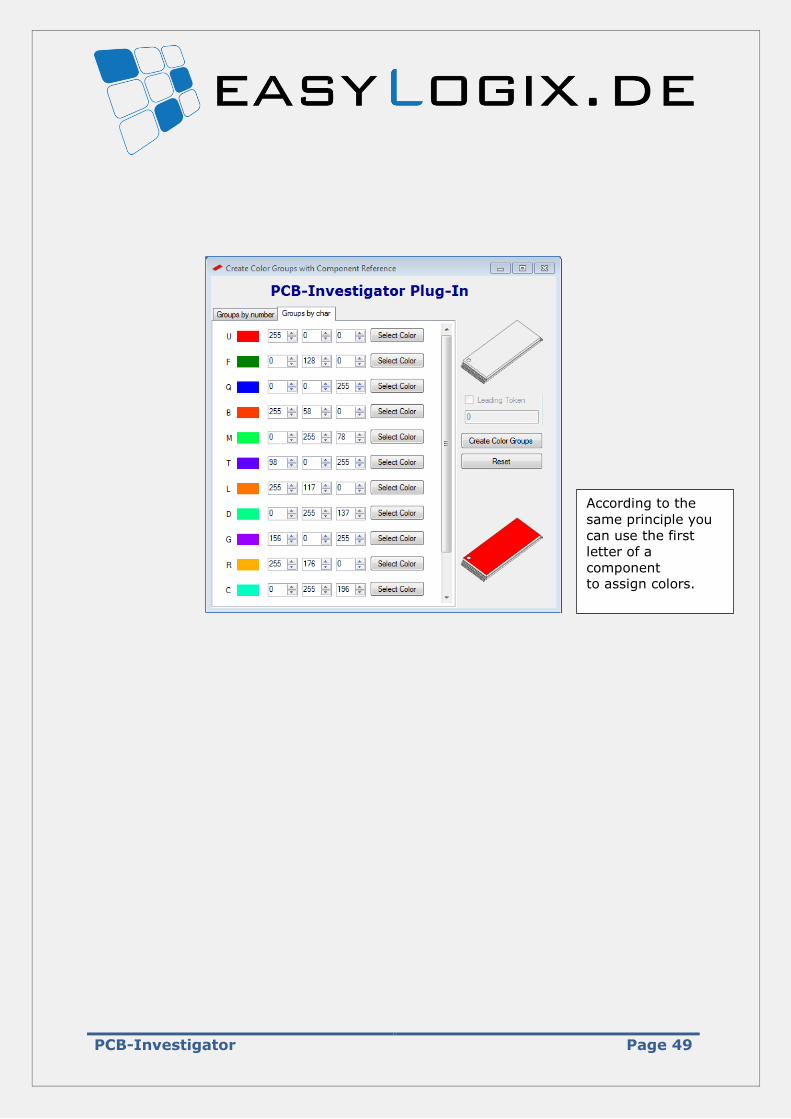
6.15 Color Group
„Color Group“ assigns certain colors to certain components. The color selection allows all windows colors.
Select colors by
entering RGB
values or by “Select
Color” with
the color dialog box
Create groups with
leading number
tokens
After choosing the
colors, assign colors to the design
PCB-Investigator Page 49
According to the
same principle you
can use the first
letter of a
component to assign colors.
PCB-Investigator Page 50
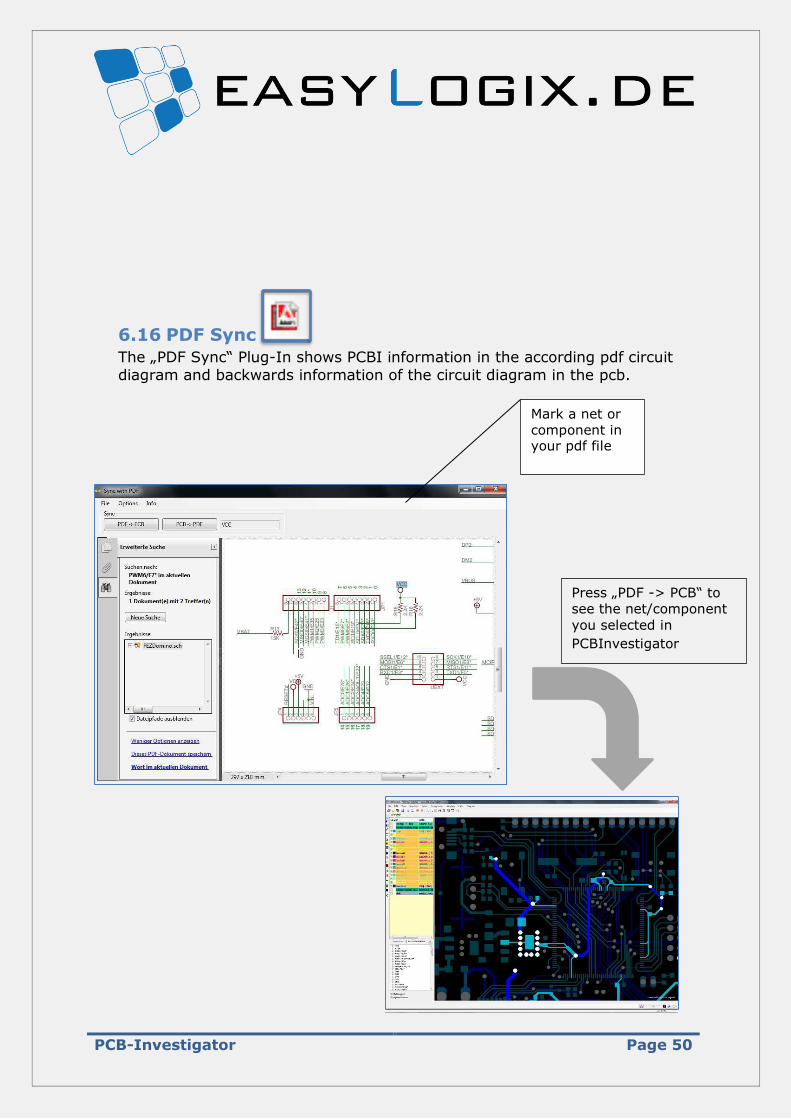
6.16 PDF Sync
The „PDF Sync“ Plug-In shows PCBI information in the according pdf circuit
diagram and backwards information of the circuit diagram in the pcb.
Mark a net or
component in your pdf file
Press „PDF -> PCB“ to
see the net/component
you selected in
PCBInvestigator
PCB-Investigator Page 51
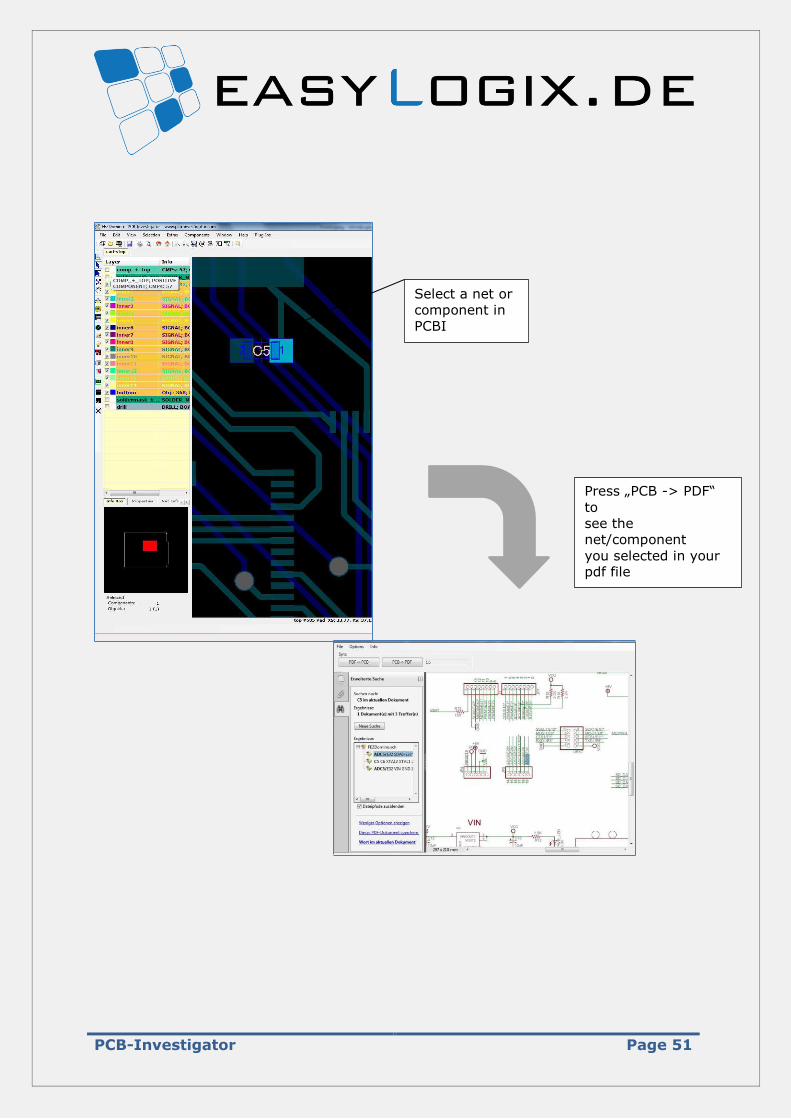
Select a net or
component in
PCBI
Press „PCB -> PDF“
to
see the
net/component
you selected in your pdf file
PCB-Investigator Page 52
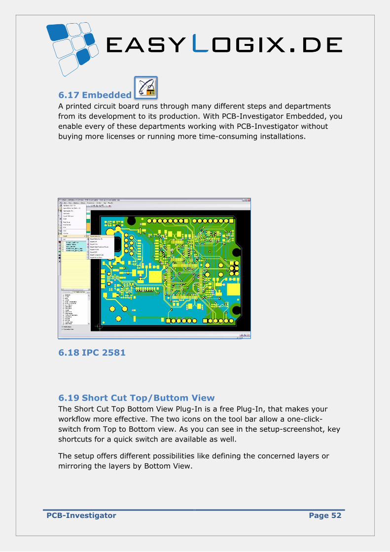
6.17 Embedded
A printed circuit board runs through many different steps and departments
from its development to its production. With PCB-Investigator Embedded, you
enable every of these departments working with PCB-Investigator without
buying more licenses or running more time-consuming installations.
6.18 IPC 2581
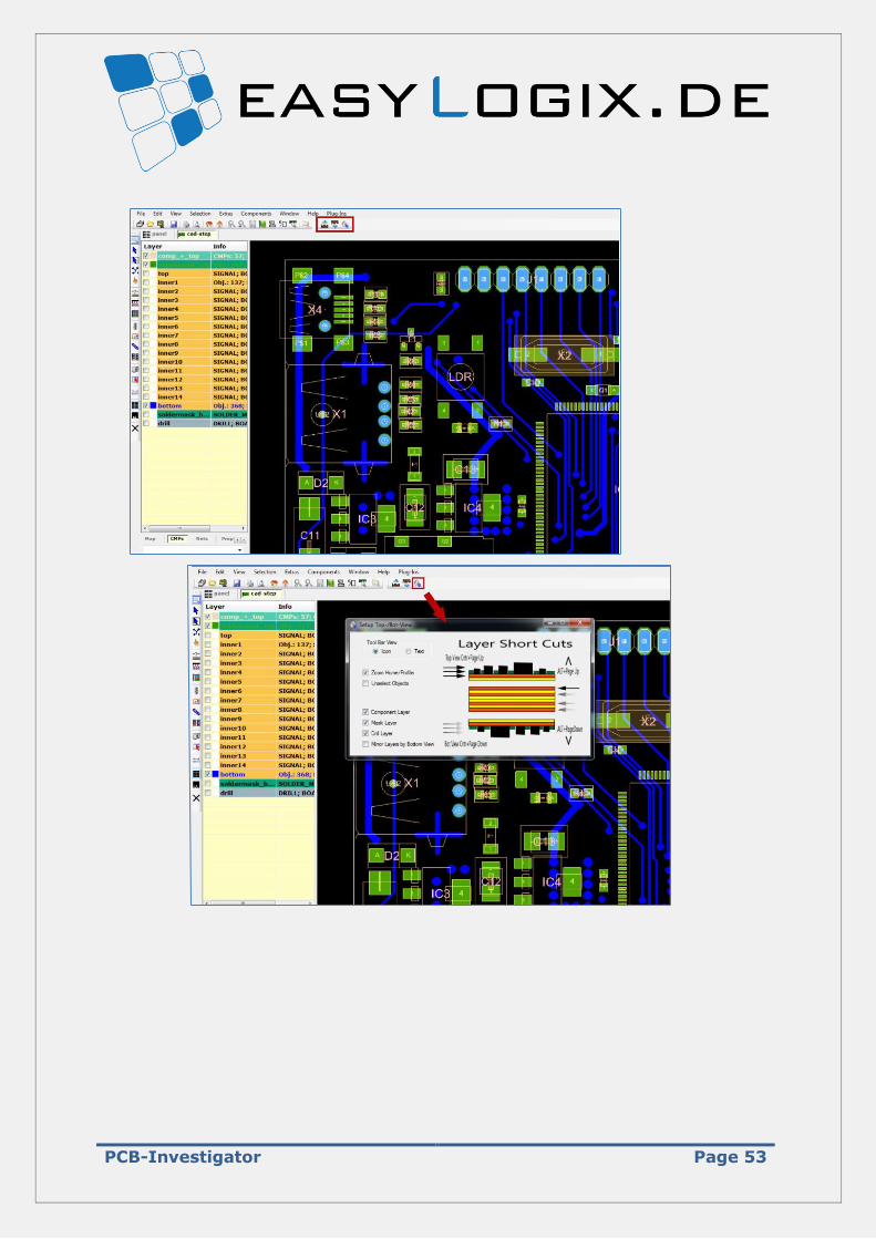
6.19 Short Cut Top/Buttom View
The Short Cut Top Bottom View Plug-In is a free Plug-In, that makes your
workflow more effective. The two icons on the tool bar allow a one-click-
switch from Top to Bottom view. As you can see in the setup-screenshot, key
shortcuts for a quick switch are available as well.
The setup offers different possibilities like defining the concerned layers or
mirroring the layers by Bottom View.
PCB-Investigator Page 53
PCB-Investigator Page 54
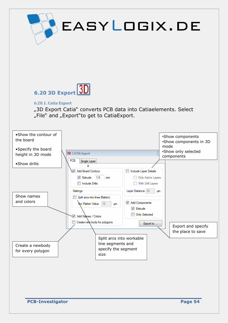
6.20 3D Export
6.20.1. Catia Export
„3D Export Catia“ converts PCB data into Catiaelements. Select
„File“ and „Export“to get to CatiaExport.
Export and specify
the place to save
•Show components
•Show components in 3D
mode
•Show only selected
components
Create a newbody
for every polygon
Show names
and colors
•Show the contour of
the board
•Specify the board
height in 3D mode
•Show drills
Split arcs into workable
line segments and
specify the segment
size
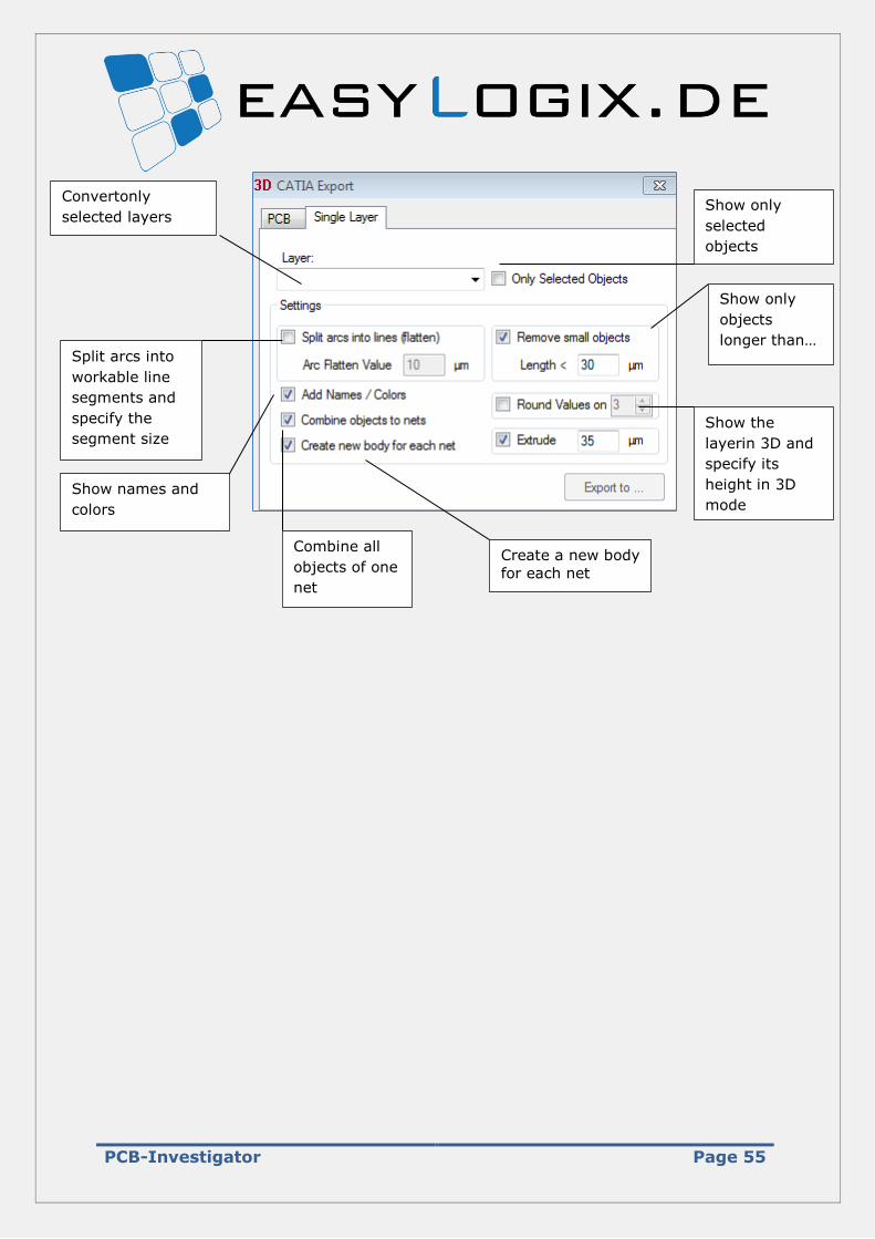
PCB-Investigator Page 55
Show only
selected
objects
Show only
objects
longer than…
Show the
layerin 3D and
specify its
height in 3D
mode
Create a new body
for each net
Combine all
objects of one
net
Show names and
colors
Split arcs into
workable line
segments and
specify the
segment size
Convertonly
selected layers
PCB-Investigator Page 56
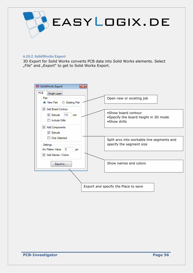
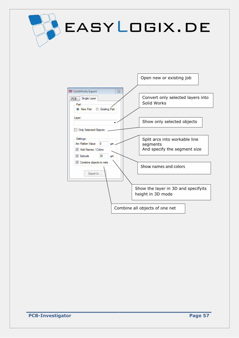
6.20.2. SolidWorks Export
3D Export for Solid Works converts PCB data into Solid Works elements. Select „File“ and „Export“ to get to Solid Works Export.
Open new or existing job
•Show board contour
•Specify the board height in 3D mode
•Show drills
Split arcs into workable line segments and
specify the segment size
Show names and colors
Export and specify the Place to save
PCB-Investigator Page 57
Open new or existing job
Convert only selected layers into
Solid Works
Show only selected objects
Split arcs into workable line
segments
And specify the segment size
Show names and colors
Show the layer in 3D and specifyits
height in 3D mode
Combine all objects of one net