Passive Wireless Sensors Fabricated by Direct‐ Writing for ... · Passive Wireless Sensors...
49
Passive Wireless Sensors Fabricated by Direct‐ Writing for Temperature and Health Monitoring of Energy Systems in Harsh‐Environments Graduate Researcher Team: Michael Comparetto a Nandhini Ranganathan b Co‐PI Team: Dr. Daryl Reynolds a Dr. Edward M. Sabolsky b Dr. Kostas Sierros b a Lane Department of Computer Science and Electrical Engineering b Department of Mechanical and Aerospace Engineering West Virginia University (WVU) 1
-
Upload
truongdung -
Category
Documents
-
view
222 -
download
0
Transcript of Passive Wireless Sensors Fabricated by Direct‐ Writing for ... · Passive Wireless Sensors...

Passive Wireless Sensors Fabricated by Direct‐Writing for Temperature and Health Monitoring of
Energy Systems in Harsh‐Environments
Graduate Researcher Team: Michael ComparettoaNandhini Ranganathanb
Co‐PI Team: Dr. Daryl Reynoldsa
Dr. Edward M. SabolskybDr. Kostas Sierrosb
aLane Department of Computer Science and Electrical EngineeringbDepartment of Mechanical and Aerospace Engineering
West Virginia University (WVU)
1

Background‐ Harsh Environment Sensing Needs
Online monitoring of energy systems in extreme conditions is required for mining/drilling, transportation, aviation, energy, chemical synthesis, and manufacturing applications.
Harsh‐environments include: High temperature (1000oC‐2000oC) High pressure (up to 1000 psi) Various pO2 levels Corrosive conditions (molten inorganics or reactive gasses)
Ability to monitor: Temperature Stress/strain within energy or reactor components Failure events Overall health
2
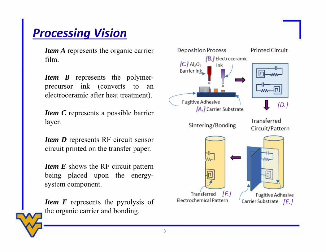
Processing Vision
3
Item A represents the organic carrierfilm.
Item B represents the polymer-precursor ink (converts to anelectroceramic after heat treatment).
Item C represents a possible barrierlayer.
Item D represents RF circuit sensorcircuit printed on the transfer paper.
Item E shows the RF circuit patternbeing placed upon the energy-system component.
Item F represents the pyrolysis ofthe organic carrier and bonding.
[D.]
[E.][F.]

1) Investigate phase formation, sintering/grain growth, and electrical properties of polymer‐derived electroceramic composites between 500‐1700 C.
2) Define processes to direct‐write through ink‐jet and robo‐casting the electroceramic composites onto oxide and polymer surfaces.
3) Develop methods to form monolithic “peel‐and‐stick” preforms that will efficiently transfer the sensor circuit to ceramic surfaces after thermal treatment.
4) Design of RF passive wireless LCR circuits and receiver (reader) antennas for communication and testing at temperature up to 1700C.
5) Demonstrate the passive wireless sensor system developed for temperature and stress/strain measurements on a SOFC repeat unit and a singular gas turbine blade prototype as example applications.
Program Objectives
4

Dr. Edward M. Sabolsky (WVU Mechanical and Aerospace Engineering) will act as PI of the program (both technical and administrative), and will be responsible for ceramics processing and sensor testing.
Dr. Kostas Sierros (WVU Mechanical and Aerospace Engineering) will lead development of micro‐patterning and robo‐casting of ceramic materials, and will be the co‐developer of the printing inks and direct‐writing tasks.
Dr. Daryl Reynolds (WVU Computer Engineering) will lead the electronics design, interfacing and circuitry, in addition to the development of the passive wireless communication and testing.
Dr. Andrew Nix (WVU Mechanical and Aerospace Engineering) 15 years of experience in turbine blade testing, and he will consult on the turbine blade demonstration testing.
Dr. Matthew Seabaugh and Mr. Gene Arkenburg (Nexceris LLC) are Director of Product Development and SOFC Group Leader, respectively. Assist in testing technology on SOFC platform.
Drs. Timothy Yosenick and Kristen Brosnan (GE Global Research) are Materials Scientist and Manager of Ceramic Structures and Processing Laboratory, respectively. Consult and mentor team for turbine blade application and demonstration.
R&D Team (Co‐PIs)
5

6
Major Milestones:Materials/Sensor FabricationM1‐ (Task 2) Down‐select composite composition for Task 3. (June 2016)M2‐ (Task 3) Define basic ink/paste formulation for printing. (June 2016)M3‐ (Task 3) Completed baseline sensor printing on oxide substrates. (January 2017)M4‐ (Task 3) First demo of pattern transfer. (March 2017)M5‐ (Task 3) First demo of circuit pattern transfer. (September 2017)
Passive Wireless Circuit Modeling and TestingM6‐ (Task 4) Completed design and testing of sensor circuit. (Sept. 2016)M7‐ (Task 4) Completed wireless coupling modeling for applications. (March 2017)
*Roughly 6‐9 Months behind on schedule due to timing for bringing graduate students into the program.
Nandhini Ranganathan (Ph.D. student)‐ materials/sensor research (started Jan. 2017)
Michael Comparetto (M.S. student)‐ electronics/wireless research (started ~Mar. 2016)
Task 2.0:Fabrication and Characterization of Polymer‐Derived Electroceramic
Composites.(Sabolsky, Ranganathan)
7

Task 2.0 Objective:
Investigate phase formation, sintering/grain growth, and electrical properties of electroceramiccomposites between 500‐1700 C.
8

Task 2.0 Approach:
Subtask 2.1 Synthesis of Multifunctional Electroceramic Compositesthrough Polymer‐Derived Precursors.‐ Silicon‐containing polymers suchas polysilane, polycarbosilanes, and polycarbosiloxanes will beinvestigated as precursors to fabricate various electroceramiccompositions. This will include the addition of fillers and reactive salts.
Subtask 2.2 Thermal Processing of Composite Compositions.‐ Sampleswill be pressed into bars, and also screen‐printed onto Al2O3 or ZrO2dense substrates (for initial observation on shrinkage effects). Thermalprocessing the materials in various atmospheres (air, inert, reducingatmosphere) will be completed up to 1700ºC.
Subtask 2.3 Composite Material Testing and Characterization.‐ Electricaltesting (at high‐temperature) and phase/chemistry characterization willbe completed on the polymer‐derived electroceramic composites.
9

Task 2.0 Current status:
Subtask 2.1 Synthesis of Multifunctional Electroceramic Compositesthrough Polymer‐Derived Precursors.‐ Silicon‐containing polymer Poly di‐ methyl siloxane (PDMS) is
investigated as precursor Fabricated various electroceramic compositions As a risk mitigation approach, lanthanum nickelate is also synthesized
and characterized.
Subtask 2.2 Thermal Processing of Composite Compositions.‐ Samples are pressed into cubes for initial observation on shrinkage
effects Screen‐printed onto ytrria stabilized zirconia substrates to initiate task 4 Thermal processing the materials in inert atmosphere is done at 1500˚C.
Subtask 2.3 Composite Material Testing and Characterization.‐ Phase/chemistry characterization is completed on the polymer‐derived
electroceramic composites.
10

Polymer‐Derived Ceramics (PDCs):
Polymers with silicon backbone attached to oxygen, carbon, nitrogen or boron atoms
Thermal processing with metals yield silicates, silicon carbides, silicon nitrides, silicon borates which are ceramic in nature.
ISSUES:Off‐gassing of short organic molecules and potentially CO/CO2
Large volumetric shrinkageCracking, voids, and delamination (if formed as films)
11

System 1: Polymer Derived Ceramics (PDCs)
• Molar ratios of Si in PDMS and molybdenum are varied to synthesize PDCs of different compositions
• Molybdenum to silicon molar ratios 1:1, 2:1, 3:1 and 4:1 are synthesized and characterized
• PDCs are fired at a constant temperature of 1500˚C in Argon atmosphere
Mold
Density study
Mix
Add crosslinking agent
Poly di‐ methyl siloxane (PDMS)
elastomer
Molybdenum Powder(2 um)
Injection Mold samples
Cure
SEM and XRD
Density study
12
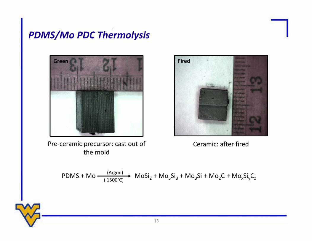
Green Fired
Pre‐ceramic precursor: cast out of the mold
Ceramic: after fired
PDMS/Mo PDC Thermolysis
PDMS + Mo MoSi2 + Mo5Si3 + Mo3Si + Mo2C + MoxSiyCz(Argon)
( 1500˚C)
13

14
As molar ratio of molybdenum is increased, both linear and volumetric shrinkage reduces due to:• Decreasing organic matter in the sample• Increasing molybdenum that forms composites with silicon in the polymer
PDMS/Mo PDC: Linear and volumetric shrinkage
020406080
100
0.0 1.0 2.0 3.0 4.0 5.0
Shrin
kage
(%)
Molar composition of Mo …
020406080
100
0.0 1.0 2.0 3.0 4.0 5.0
Shrin
kage
(%)
Molar composition of Mo …
Linear Shrinkage Volumetric Shrinkage

As molar ratio of molybdenum is increased, • Weight loss decreases since there is less organic matter that decomposes and more composites are formed
• Density increases because, of less organic decomposition, there is less voids and more densification
020406080
100
0 2 4 6Perc
ent t
heor
etic
al
dens
ity (%
)
Molar composition of Mo in the sample
PDMS/Mo PDC: Weight loss and Densification
020406080
100
0 2 4 6
Wei
ght l
oss
(%)
Molar composition of Mo in the sample
Weight loss Densification
15

16
XRD analysis of PDMS/Mo PDCs
• Major phase Mo and minor phases are Mo2C and Mo3Si
• Major phase Mo3Si and minor phases are Mo5Si3 and Mo
20 30 40 50 60 70
Inte
nsity
(-)
Mo:Si=1:1Mo3SiMo2CMo
20 30 40 50 60 70
Inte
nsity
(-)
Mo:Si=4:1Mo3SiMoMo5Si3
* Silicides are metallic in nature; carbides are semiconducting in nature.
2 theta (deg.) 2 theta (deg.)

17
SEM Micrographs of PDMS/Mo‐based PDCs
• Grain sizes are smaller • Grains are interconnected on 3D matrix
• More gray regions‐ Mo, Lighter gray regions‐ Mo2C
50 um
Mo:Si = 1:1
50 um
Mo:Si = 4:1
• Grain sizes are larger• Less voids, interconnected on 3D matrix
• More gray regions‐ Mo3Si, Lighter gray regions‐ Mo5Si3
porosity
Mo3Si
Mo5Si3
porosity
Mo
Mo2C

System 2: Conductive oxide‐ Lanthanum Nickelate
Lanthanum Carbonate Nickel Oxide
Attrition Mill
Calcine
Attrition Mill
Particle size characterize
Formulate ink suspension
18
20 40 60
Inte
nsity
(-)
2 Theta (deg.)
La2NiO4
X‐Ray Diffraction of lanthanum nickelate

Task 2.0 Summary:
19
Task 2.0 Near‐term Future Work:
Synthesized different silicide‐carbide electroceramics using PDMS and molybdenum Characterized Phase formation Characterized Thermal processing Quantified shrinkage and Densification
Synthesized lanthanum nickelate and characterized
Synthesize: Silicide‐carbide systems with active (W, Ta) and inactive (Al2O3, ZrO2) fillers Silicide‐carbide systems using different silicon containing polymer precursors
Effects of thermal processing Study Phase formation

Task 3.0:Direct‐Writing, Patterning, and Transfer of the Sensor System.
(Sierros/Sabolsky/Ranganathan)
20

Task 3.0 Objectives:
To define processes to direct‐write through ink‐jet and robo‐casting the polymer‐derived electroceramic composites onto oxide and polymer surfaces.
To develop a method to transfer the pattern from an organic film to a ceramic surface and bond after thermal treatment.
21

Task 3.0 Approach:
Subtask 3.1 Direct‐Writing Ink Development.‐ Develop inks within a permissible surface tension and viscosity level. Direct‐writing with Nordson EFD Performus VI robo‐printer.
Subtask 3.2 Direct‐Writing/Patterning and Drying Characterization.‐General process for droplet deposition, drying, and thermolysis will be defined, which includes methods to alter the wetting and drying characteristics of the deposited composite solutions.
Subtask 3.3 Thermal Processing Development and Structure Tailoring.‐ Ink deposited directly on oxide surfaces will undergo thermal treatment defined by thermal schedules in Task 2 as a starting point.
Subtask 3.4 Baseline Sensor Testing and Design Optimization.‐ Three initial sensor configurations (without passive communication circuit) will be designed, with focus on temperature and strain measurements. The electrical performance testing will be completed at high‐temperature (500‐1700C).
Subtask 3.5 “Peel‐and‐Stick” Development.‐ Investigate methods to transfer the sensor circuit/system to the active energy system component, which will be represented by alumina and zirconia substrates.
22
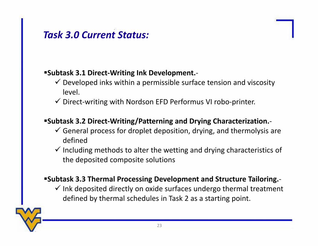
Task 3.0 Current Status:
23
Subtask 3.1 Direct‐Writing Ink Development.‐ Developed inks within a permissible surface tension and viscosity
level. Direct‐writing with Nordson EFD Performus VI robo‐printer.
Subtask 3.2 Direct‐Writing/Patterning and Drying Characterization.‐ General process for droplet deposition, drying, and thermolysis are
defined Including methods to alter the wetting and drying characteristics of
the deposited composite solutions
Subtask 3.3 Thermal Processing Development and Structure Tailoring.‐ Ink deposited directly on oxide surfaces undergo thermal treatment
defined by thermal schedules in Task 2 as a starting point.

(a) Direct writing Ag ink for flexible
electrodes
Initial Robo‐Casting Evaluation:
(b) Nozzle-based robotic deposition (NBRD) system
and ink printing.
Ink formulation
Ink characterization
Wetting,Bonding on substrate
Viscosity,Surface tension
Print parameters optimization
Process Variables:Tip geometryGauge sizePressureLine speedHeight
Characterization
Two Systems Initially Evaluated Last Quarter:1) PDMS/Mo Ink (PDMS is the vehicle)2) LNO Suspension Ink (Terpineol vehicle)
24

050000
100000150000200000250000300000350000400000450000
0 0.2 0.4 0.6 0.8 1 1.2 1.4 1.6
Visc
osity
(cP)
Shear rate (s-1)
4:1 polymer pre‐ceramic precursor rheology
25
System 1: PDMS/Mo Ink Rheology
Brookfield DV‐II+ Pro (plate‐on‐plate)
Key Rheology Parameters:1) Shear thinning in order to
extrude ink and lock the pattern2) Viscosity between 300 P – 200 P
is desired at shear rates ~0.3 s‐13) Optimal wetting to retain
dimensions

• 4:1 composition printed and thermolysed at 1500 ˚C• Thickness of the line is 1 mm• Tip type‐ stainless steel, Gauge size‐ 22, Pressure of extrusion‐30 psi, Line speed‐ 10mm/s and Height‐ ½ diameter of the tip
Unfired PDC Fired PDC
26
Initial Printing Evaluation of PDMS/Mo Precursor

• LNO particulate suspensions are shear thinning as expected with apparent viscosity in workable range of 12 P (at shear rate of ~5 s‐1)
• Screen printing of inductor and capacitor using lanthanum nickelate ink on yttria stabilized zirconia substrate
02000400060008000
10000120001400016000
0 5 10 15 20 25 30
Visc
osity
(cP)
Shear rate (s-1)
System 2: Conductive oxide‐ Lanthanum Nickelate
Inductor on YSZ Capacitor on YSZ
27

Task 3.0 Summary:
Task 3.0 Near‐term Future Work:
Direct‐write preceramic precursor onto oxide substrates and bond Screen print (to initiate task 4) silver ink and conductive oxide
suspension and bond to the surface
Robo‐ cast preceramic ink precursor onto oxide substrates and optimize firing temperature for optimum density
Achieve print resolution <100 um to print next generation LCR circuits
28

Task 4.0: Passive Wireless Communication
Circuit Design and Testing.(Reynolds/Comparetto)
29

Task 4.0 Objectives:
• To design and model a passive wireless LCR circuit and receiver (reader) antennas for communication.
• To fabricate and test the sensor design and circuit at room temperature and up to 1700C.
30
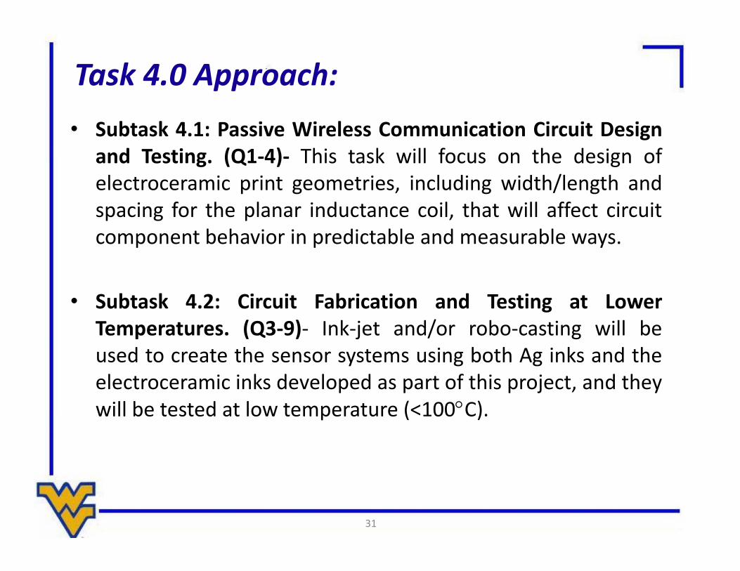
Task 4.0 Approach:• Subtask 4.1: Passive Wireless Communication Circuit Design
and Testing. (Q1‐4)‐ This task will focus on the design ofelectroceramic print geometries, including width/length andspacing for the planar inductance coil, that will affect circuitcomponent behavior in predictable and measurable ways.
• Subtask 4.2: Circuit Fabrication and Testing at LowerTemperatures. (Q3‐9)‐ Ink‐jet and/or robo‐casting will beused to create the sensor systems using both Ag inks and theelectroceramic inks developed as part of this project, and theywill be tested at low temperature (<100C).
31

Task 4.0 Current Status:• Built 3D and 2D models and simulations of sensors in ANSYS
Software• Built a low temperature testbed
• Generated a data set of temperature signatures for low temperature
• Performed preliminary low temperature passive wireless temperature sensing tests
• Verified that preliminary sensors can accurately measure their environment’s temperature
32

ANSYS Software
• What is ANSYS Software?– ANSYS Maxwell is a premier low frequency electromagnetic field
simulator– The software utilizes finite element analysis to simulate the
inductance, mutual inductance, capacitance, EM fields, and many other key features of our 3D or 2D models of our sensors
• Why is this important to the project?– Reduces costs– Adds flexibility– Provides sensitivity analysis– Provides control of the environment– High speed calculations and solutions– Helps design experimental plans to test
33

ANSYS Designs
• Square Planar Inductor • Interdigitated Capacitor
34
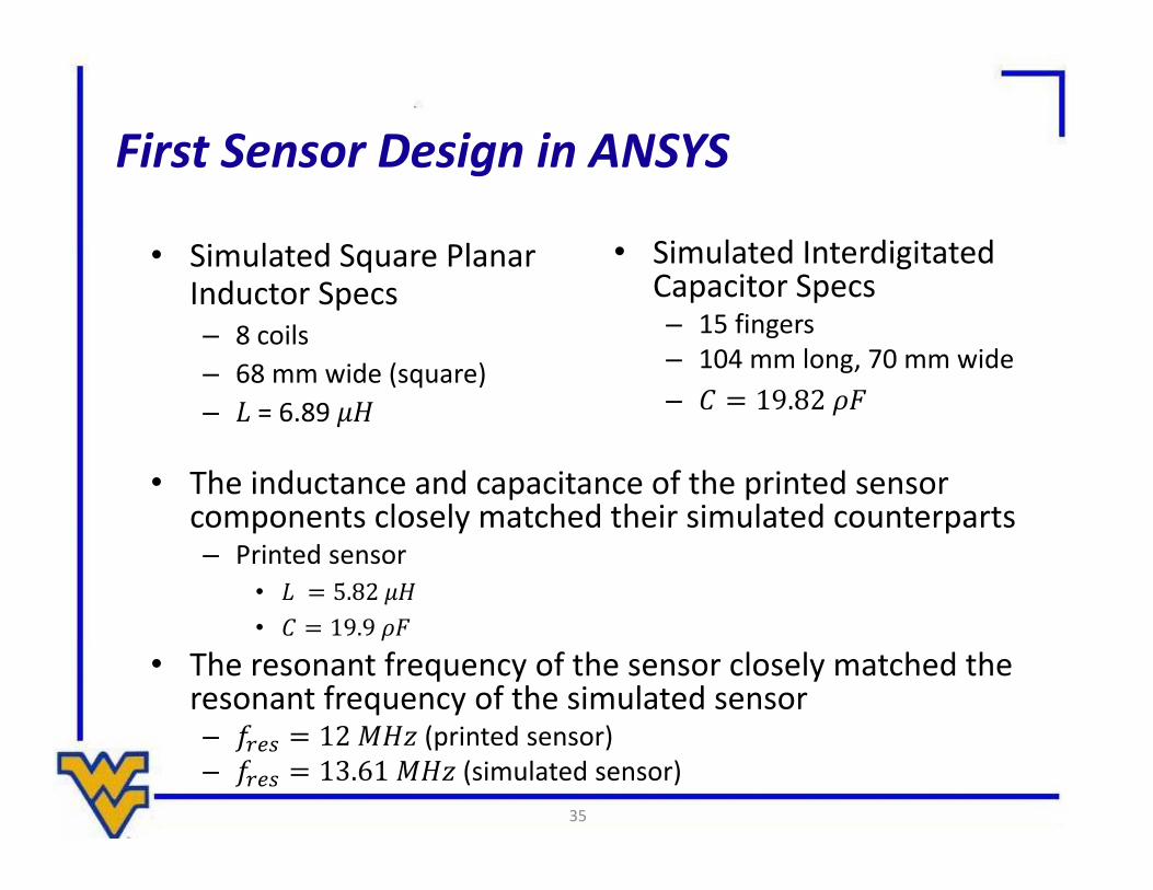
First Sensor Design in ANSYS
• The inductance and capacitance of the printed sensor components closely matched their simulated counterparts– Printed sensor
• 5.82• 19.9
• The resonant frequency of the sensor closely matched the resonant frequency of the simulated sensor– 12 (printed sensor)– 13.61 (simulated sensor)
• Simulated Interdigitated Capacitor Specs– 15 fingers– 104 mm long, 70 mm wide– 19.82
• Simulated Square Planar Inductor Specs– 8 coils– 68 mm wide (square)– = 6.89
35

ANSYS EM simulation
• Simulation of the EM field around the square planar inductor
36

ANSYS Sensor Development
• Because we have laid the ground work in building the 3D simulations of our sensor– We can now quickly change the models of our sensors and tailor them to what we need
2 in by 2 in Sensor Design 1 in by 1 in Sensor Design
37

Challenges Faced in Wireless Communications
1
1
38

Passive Wireless Temperature Sensor
• Preliminary passive wireless low temperature senor– Silver Ink on reflective
paper– Next phase of temperature
testing will use ceramic based sensors.
39

Passive Wireless Temperature Sensing Testbed
Signal GeneratorTransmit and Receive SensorsSpectrum Analyzer
Hot Plate
40
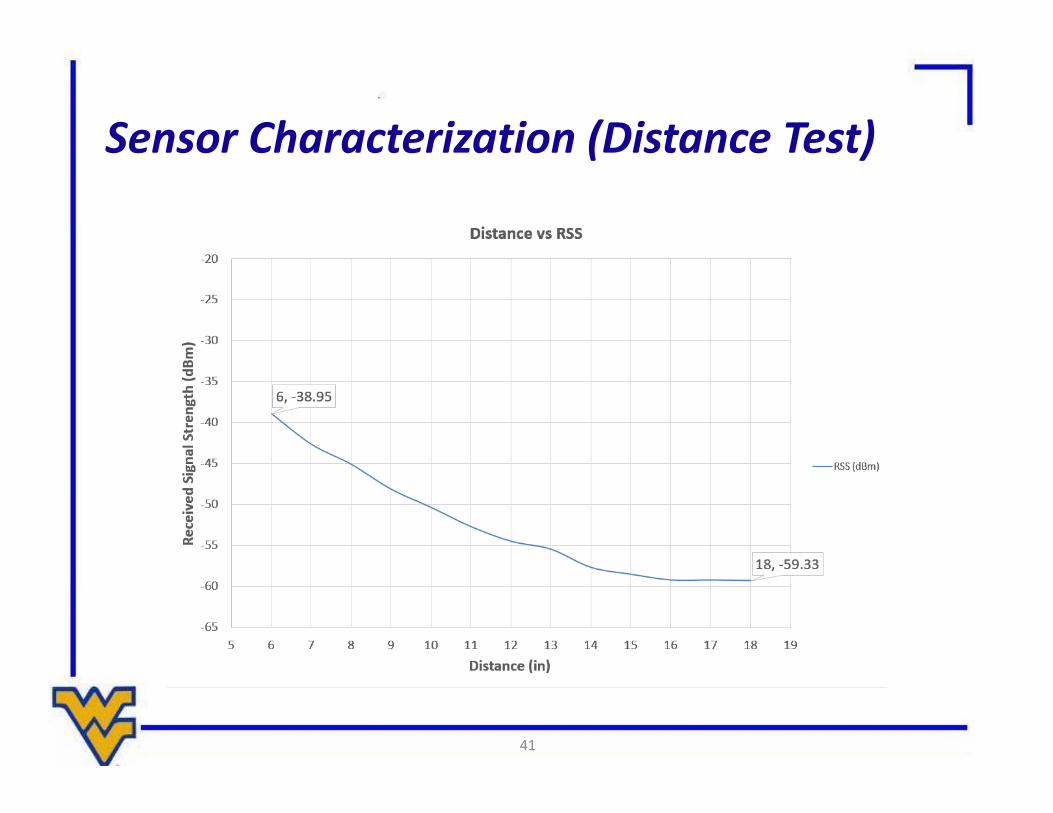
Sensor Characterization (Distance Test)
41

Sensor Characterization (Frequency Response)
42

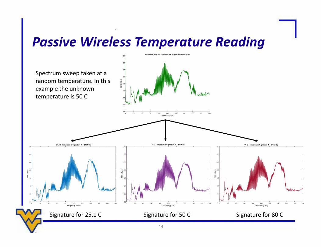
Passive Wireless Temperature Reading
• We use a large band of spectrum (many degrees of freedom) to measure temperature– This is a more robust method– Allows for the application of advanced signal processing methods from fields
like wireless communications, Radar, digital image processing, Radio Astronomy
• In the past, other works have used peak tracking (few degrees of freedom)– Heavily reliant on the peak’s sensitivity to changes in temperature
• Method 1: Correlation– ∗ – where is the signature waveform for temperature , is the unknown
temperature frequency sweep, and is the estimated temperature– Choose the temperature signature the maximizes the correlation
• This is the closest match to the unknown temperature
43
Passive Wireless Temperature Reading
Spectrum sweep taken at a random temperature. In this example the unknown temperature is 50 C
Signature for 25.1 C Signature for 50 C Signature for 80 C
44

Passive Wireless Temperature Reading
Method Correlation Abs. Error
25.1 C 0.9990 1078
50 C 0.9997 542.1
80 C 0.9994 803.3
Spectrum sweep taken at a random temperature. In this example the unknown temperature is 50 C
25.1 C
50 C
80C
45

Absolute Difference between Unknown Temperature and Temperature Signatures
25.1 C
80 C
50 C
46
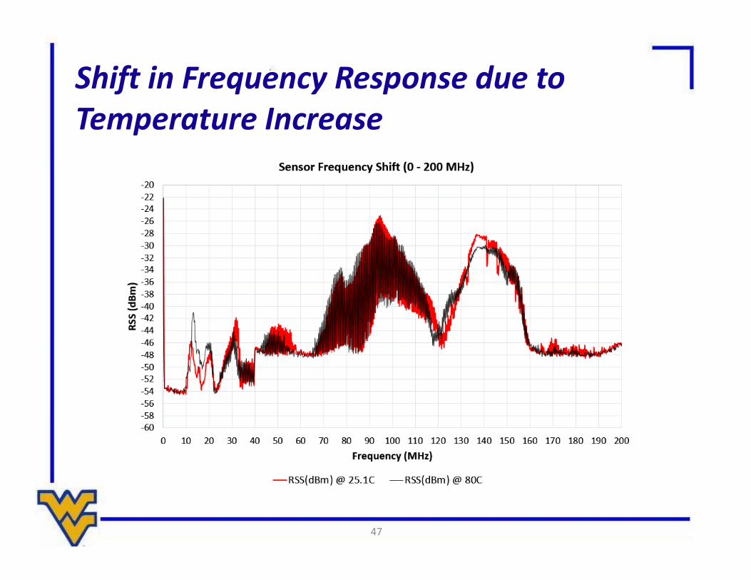
Shift in Frequency Response due to Temperature Increase
47
Task 4.0 Summary:
48
Task 4.0 Near‐term Future Work:
• Completed preliminary low temperature passive wireless temperature sensing– Built 3D models and simulations of sensor designs– Created a low temperature sensing testbed– Demonstrated ability to accurately sense the temperature of the sensor’s environment
– Verified the accuracy of the 3D models and simulations
• Continue to build 3D models of sensor to fit inside of 2in and 1in squares
• Build a high temperature testbed– Generate a high temperature database– Start running high temperature sensing tests

We would like to thank U.S. Department of Energy (DOE) forsanctioning this project DE‐FE0026171.
Jessica Mullen, project manager at U. S. Department of Energy,is greatly appreciated for her insight and valuable guidance.
We also would like to acknowledge Dr. Wei Ding, Dr. MarcelaRedigolo and Mr. Harley Hart for their cooperation andvaluable assistance in the WVU Shared Facilities.
Kindly acknowledge Faculty and staff of West VirginiaUniversity for their support.
Acknowledgments:
49