Partial Discharge Analysis
49
Simulation of Partial Discharge Patterns Using PSPICE SUBMITTED BY: KUNTAL SATPATHI (07/EE/02) INDRANIL DEBNATH (07/EE/08) SUVRA KANTI PAL (07/EE/18) SOURAV BISWAS (07/EE/22) SUPRIYO MONDAL (07/EE/35) HALDIA INSTITUTE OF TECHNOLOGY SUBMITTED FOR THE DEGREE OF BACHELOR OF TECHNOLOGY IN THE DEPARTMENT OF ELECTRICAL ENGINEERING
-
Upload
kuntal-satpathi -
Category
Documents
-
view
110 -
download
8
description
PD analysis due to voids in dielectrics
Transcript of Partial Discharge Analysis

1
Simulation of Partial Discharge Patterns Using
PSPICE
SUBMITTED BY:
KUNTAL SATPATHI (07/EE/02)
INDRANIL DEBNATH (07/EE/08)
SUVRA KANTI PAL (07/EE/18)
SOURAV BISWAS (07/EE/22)
SUPRIYO MONDAL (07/EE/35)
HALDIA INSTITUTE OF TECHNOLOGY
SUBMITTED FOR THE DEGREE OF
BACHELOR OF TECHNOLOGY IN THE DEPARTMENT OF
ELECTRICAL ENGINEERING

2
CONTENTS
Topic Page No.
CHAPTER 1
1.1 Partial Discharge Analysis 5
1.2 Causes of Partial Discharge 5
1.3 Partial Discharge Emissions 6
1.4 Effect of PD on Electrical Insulation Health 6
1.5 PD as a symptom of ageing 7
1.6 Benefits of PD monitoring 7
1.7 Classification of Partial Discharge 8
1.7.1 External Partial Discharge 10
1.7.2 Internal Partial Discharge 10
1.8 Literature Survey 11
1.9 Present Work 12
CHAPTER 2
2.1 Partial Discharge Equivalent Circuit 13
2.2 Simulation Model 22
2.2.1 Explanation of the Model 22
2.3 Parameters on which Partial Discharge Depends 23
2.3.1 Physics behind Partial Discharge 23
CHAPTER 3
3 Simulation Results 25
3.1 Simulation results for different supply voltages 25
3.1.1 Variation of average number of breakdown with
supply voltage
29
3.2 Simulation results for voids of different sizes 30
3.3 Simulation results for different residual voltage 35
3.4 Simulation results for different discharge
inception voltages
38
3.5 Simulation results for different permittivity of the
dielectric
41
3.6 Simulation results for different supply frequency 43
3.7 Verifications of results with that of Field Based
Results
46
CHAPTER 4
4.1 Conclusion 48
4.2 Future Scope of the Work 48
4.3 References 49

3
To
The Head of the Department
Department of Electrical Engineering
Haldia Institute of Technology
HIT/ ICARE Complex
P. O.: Hatiberia, Haldia
Midnapore(E), West Bengal-721 657
Respected Sir,
In accordance with the requirements of the degree of Bachelor of Technology in the department of Electrical
Engineering, Haldia Institute of Technology, we present the following thesis entitled “Simulation of Partial
Discharge Patterns Using Pspice”. This work was performed under the supervision of Mr. Prithwiraj Das.
We declare that the work submitted in this thesis is our own and the text and reference has not been previously
submitted for a degree at the institute.
Yours Sincerely,
………………………………………..
KUNTAL SATPATHI (07/EE/02)
UNIVERSITY ROLL NO.: O71030116002
…………………………………………
INDRANIL DEBNATH (07/EE/08)
UNIVERSITY ROLL NO.: 071030116008
……………………………………….…
SUVRA KANTI PAL (07/EE/18)
UNIVERSITY ROLL NO.: 071030116018
…………………………………………..
SOURAV BISWAS (07/EE/22)
UNIVERSITY ROLL NO.: 071030116022
……………………………………………
SUPRIYO MONDAL (07/EE/35)
UNIVERSITY ROLL NO.: 071030116035

4
ACKNOWLEDGEMENT
Apart from the efforts of us, the success of this project depends largely on the encouragement
and guidance of many others. We take this opportunity to express our gratitude to the people who
have been instrumental in the successful completion of this project.
First and foremost, we really take this opportunity to express our gratitude to our project guide,
Mr. Prithwiraj Das, Department of Electrical Engineering, H.I.T., Haldia. His precious guidance,
suggestions and encouragement throughout the project, which helped us a lot to our project work.
We are also thankful to Dr. Prithwiraj Purkait, Head of the Department, Electrical
Engineering Department, H.I.T., Haldia, for his encouragement and also give us this opportunity to
do this project work.
We are highly grateful for their constant support and help.
5
CHAPTER 1
1.1 PARTIAL DISCHARGE ANALYSIS
Partial discharges are electrical “sparks” that do not completely bridge the electrodes and
which exist in nearly all high voltage electrical machinery. The phenomena results in high frequency,
low voltage signals on the phase leads. Over time, the degradation and discharges become larger until
a full discharge is obtained leading to failure of the equipment. Partial discharges are small electrical
sparks that occur within the electric insulation of switchgear, cables, transformers, and windings in
large motors and generators. Partial Discharge Analysis is a proactive diagnostic approach that uses
partial discharge (PD) measurements to evaluate the integrity of this equipment. Each discrete PD is a
result of the electrical breakdown of an air pocket within the insulation. PD measurements can be
taken continuously or intermittently and detected on-line or off-line. PD results are used to reliably
predict which electrical equipment is in need of maintenance. Just as every material has a
characteristic tensile strength, each material also has an electrical breakdown (dielectric) strength that
represents the electrical intensity necessary for current to flow and an electrical discharge to take
place. Common insulating materials such as epoxy, polyester, and polyethylene have very high
dielectric strengths. Conversely, air has a relatively low dielectric strength. Electrical breakdown in
air causes an extremely brief (lasting only fractions of a nanosecond) electric current to flow through
the air pocket. The measurement of partial discharge is, in fact, the measurement of these breakdown
currents.
Electric equipment can suffer from a variety of manufacturing defects or operating problems
that impair its mechanical reliability. The electrical insulation of motors and generators is susceptible
to:
Thermal stress
Chemical Attack
Abrasion due to excessive oil movement
In all cases, these stresses will weaken the bonding properties of the epoxy or polyester resins
that coat and insulate the windings. As a result, an air pocket develops in the windings. Not only do
partial discharge levels provide early warning of imminent equipment failure, but partial discharge
also accelerates the breakdown process. The excessive arcing between ground and conductor within
the insulation will, in time, compromise the dielectric strength and mechanical integrity of the
winding insulation. Once this happens, a ground fault or a phase-to-phase fault is inevitable.
1.2 CAUSES OF PARTIAL DISCHARGE
Partial discharge can occur at any point in the insulation system, where the electric field
strength exceeds the breakdown strength of that portion of the insulating material. Partial discharge
can occur in voids within solid insulation, across the surface of insulating material due to

6
contaminants or irregularities, within gas bubbles in liquid insulation or around an electrode in gas
(corona activity).
Partial discharge may originate at one of the electrode or occur in a cavity in the dielectric. The
air or gas cavities are one of the most wide spread types of localized defect. Due to the fact that the
dielectric permittivity of air is few times less than the dielectric filed intensity in the gas layer can
considerably exceed the average field intensity in the insulator.
Therefore in the number of cases ionization process start even the working voltage. The sum
total of this ionization process is called the “partial discharge” since they cover a small part of total
distance between the electrodes. Once begin PD causes progressive deterioration of insulating
materials ultimately leading to electric breakdown. PD can be prevented through careful design and
material is confirmed using PD detector equipment during the manufacturing stage as well as
periodically through the equipments useful life. PD prevention and detection are essential to ensure
reliable, long term operation of HV equipment used by electric power utilities.
1.3 PARTIAL DISCHARGE EMISSIONS
Partial discharges emit energy as:
Electromagnetic emissions, in the form of radio waves, light and heat
Acoustic emissions, in the audible and ultrasonic ranges
Ozone and nitrous oxide gases
1.4 EFFECT OF PD ON ELECTRICAL INSULATION HEALTH
PDs as ionization events produce different forms of energy and many types of reactive
chemical species (electrons, ions, excited species, meta-stables, acidic by-products, etc). Insulating
materials (dielectrics) in contact with PDs experience faster aging rates as thermal, mechanical and
chemical degradations take place at the corona-to-insulation interface. The PDs can then in
combination with operating and environmental stresses, “electrostatically” machine paths between the
high voltage and ground. The gradual reduction in voltage withstand capability will ultimately lead to
the failure of the insulation system during a voltage surge or a severe load swing for example.
Vibration and contamination are also known to exacerbate the effects of PD on insulation and
accelerate ageing.

7
1.5 PD AS A SYMPTOM OF AGEING:
It is often wrongly believed that PD by itself can quickly fail a medium or high voltage
micaceous insulation system. While corona by itself contributes to that it is the combination of
multiple stresses as highlighted above that creates fast insulation degradation. PD events serve as very
useful indicators of how far degradation has progressed and are how fast it is progressing. An
advanced PD data interpretation and a careful diagnostics work is always needed for a reliable
machine health assessment. PD activity can be very sensitive to contamination due oil, conductive
dust such as metal or carbon powder. It can also detect winding vibration and winding support system
issues. Excessive thermal stress can also lead to a gradual degradation of stress grading systems
leading to excessive local corona around the non linear voltage grading coating.
1.6 BENEFITS OF PD MONITORING:
Electrical equipments are among the most expensive and critical assets in power and process
plants. Their impact is great on profit and revenue generation. Their production and management cost
is high, and failures almost always lead to catastrophic losses. Electrical systems are being operated at
higher stress levels (thermal and cycling), even while systems are aging - which affects both the life
and the reliability of the assets. Whether continuous or periodic PD testing can enable true Condition
Based Maintenance (CBM) and reduce both operating and repair costs of electrical assets. If
performed over the long term and a reliable trend established PD testing can help:
Eliminate unplanned outages and lost profit due to system downtime
Reduce maintenance costs by extending time between planned outages
Increase availability and operating efficiency through greater system reliability
Improve risk management and reduce catastrophic failures
Improve worker safety
Today‟s asset managers are facing the increased challenge of maximizing profit from their aging
electrical infrastructure with fewer qualified technical in-house resources, stricter regulatory
requirements for worker safety, and shrinking maintenance budgets. Advances in technology,
including the use of Partial Discharge testing, are giving maintenance managers new tools to achieve
improved reliability and performance of critical electrical assets.
8
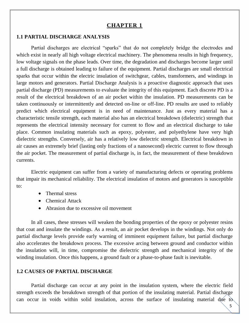
1.7 CLASSIFICATION OF PARTIAL DISCHARGE
There are various types of partial discharges.
1. Corona Discharge- these occur due to non-uniform field on the sharp edges of the conductor
subjected to high voltage especially when the insulation provided is air or gas or liquid.
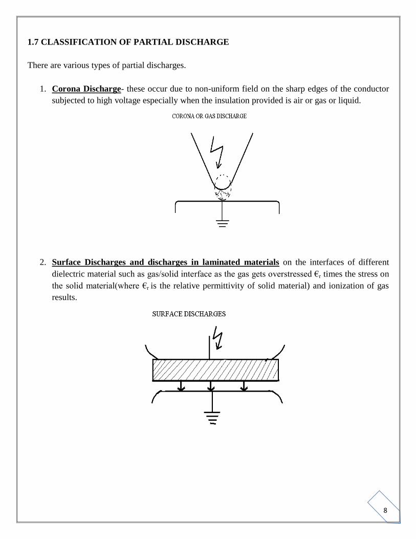
2. Surface Discharges and discharges in laminated materials on the interfaces of different
dielectric material such as gas/solid interface as the gas gets overstressed €r times the stress on
the solid material(where €r is the relative permittivity of solid material) and ionization of gas
results.
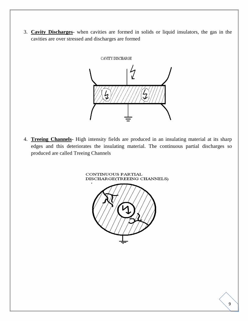
9
3. Cavity Discharges- when cavities are formed in solids or liquid insulators, the gas in the
cavities are over stressed and discharges are formed
4. Treeing Channels- High intensity fields are produced in an insulating material at its sharp
edges and this deteriorates the insulating material. The continuous partial discharges so
produced are called Treeing Channels

10
1.7.1 External Partial Discharge
External Partial Discharge is the process which occurs external to the equipment e.g. on
overhead lines, on armature.
1.7.2 Internal Partial Discharge
It is a process of electrical discharge which occurs inside a closed system (discharge in voids,
treeing, etc). This kind of classification is essential for the PD measuring system as external
discharges can be nicely distinguished from internal discharges. Partial discharge measurement has
been used to assess the life expectancy of insulating materials. Even though there is no well defined
relationship, yet it gives sufficient idea of the insulating property of the material. Partial discharges on
insulation can be measured not only by electrical methods but by optical, acoustic and chemical
methods also. The measuring principles are based on energy conversion process associated with
electric discharges such as emission of electromagnetic waves, light, noise, or formation of chemical
compounds. The oldest method and simplest but less sensitive method is the method of listening to
hissing sound coming out of partial discharge. A high value of loss factor tanδ is an indication of
occurrence of partial discharge in the material. This is also not a reliable measurement as the
additional losses generated due to application of of high voltage are localized and can be very small
in comparison to the volume of losses resulting from polarization process. Optical methods are used
for only transparent materials. Acoustic detection methods using ultrasonic transducers have,
however, been used with some success. The most modern and the most accurate methods are the
electrical methods. The main objective here is to separate impulse currents associated with Partial
Discharge from any other phenomenon.

11
1.8 LITERATURE SURVEY
The PD analysis being very important regarding the industrial point of view, it is continuously
being monitored in the industry. Also there are various methods of determining the PD analysis. Tests
and research has been carried out to determine the PD analysis. The PD analysis can be done by
various methods such as using wavelet transform, MATLAB, PSPICE.
Even many MNCs such as General Electric, Schneider Electric have developed certain
methods to determine the partial discharge and they also assist their customers. GE provides various
installations and testing option for PD measurements. Using phase resolved data acquisition the
insulation experts continuously monitor the equipments.
Using Principal Component Analysis (PCA) the research regarding the PD patterns has been
carried out in the transformer windings. Also partial discharge analyzer DDX-9101 is used with the
PCA. The PD analysis is done by locating fault in transformer and other electrical equipments.
Detection of fault location and discharge magnitude of the equipment is done by PD analyzer DDX-
9101. In this partial discharge analyzer, direct partial discharge magnitude, voltage level and wave
shape is got by which one can easily analyze the fault location.
Also mathematical models based on MATLAB have been used for investigating the partial
discharge processes in single layer solid insulation. There are chosen and calculated parameters of the
model. There are done evaluation of model marginal parameters, and their influence upon the final
results.

12
1.9 PRESENT WORK
Here we are trying to simulate the PD patterns and study its properties by using PSPICE. The
void is represented by the capacitor with parallel resistor. The BJT has been used as a switching
device. The BJT is initiated by the Schmitt trigger when the upper threshold voltage is reached, and
the BJT is switched off when the lower threshold voltage is reached in the Schmitt trigger. The
voltage follower circuit is cascaded with the Schmitt trigger to avoid loading effect.
The upper and the lower threshold voltages are determined by variation of the resistances. The
n-p-n and p-n-p transistors are used for the switching purpose in positive and negative half cycles.
Once the upper threshold voltage is reached the capacitor which represents the void,
discharges and thus the voltage across the capacitor reduces till the voltage reduces below the lower
threshold voltage. Then again the voltage rises and same process repeats.
The voltage follower circuit is used following the Schmitt trigger and then an amplifier is used
which gives sufficient voltage to trigger the base of the transistor.
13
CHAPTER 2
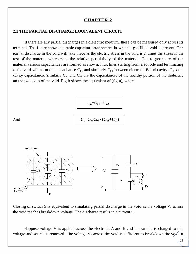
2.1 THE PARTIAL DISCHARGE EQUIVALENT CIRCUIT
If there are any partial discharges in a dielectric medium, these can be measured only across its
terminal. The figure shows a simple capacitor arrangement in which a gas filled void is present. The
partial discharge in the void will take place as the electric stress in the void is €r times the stress in the
rest of the material where €r is the relative permittivity of the material. Due to geometry of the
material various capacitances are formed as shown. Flux lines starting from electrode and terminating
at the void will form one capacitance Cb1 and similarly Cb2 between electrode B and cavity. Cc is the
cavity capacitance. Similarly Ca1 and Ca2 are the capacitances of the healthy portion of the dielectric
on the two sides of the void. Fig-b shows the equivalent of (fig-a), where
Ca=Ca1 +Ca2
And Cb=Cb1Cb2 / (Cb1+Cb2)
Closing of switch S is equivalent to simulating partial discharge in the void as the voltage Vc across
the void reaches breakdown voltage. The discharge results in a current ic
Suppose voltage V is applied across the electrode A and B and the sample is charged to this
voltage and source is removed. The voltage Vc across the void is sufficient to breakdown the void. It
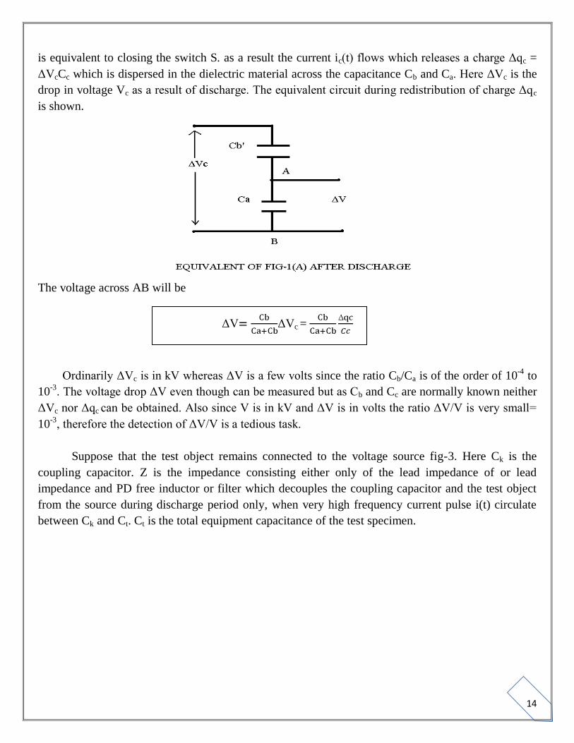
14
is equivalent to closing the switch S. as a result the current ic(t) flows which releases a charge Δqc =
ΔVcCc which is dispersed in the dielectric material across the capacitance Cb and Ca. Here ΔVc is the
drop in voltage Vc as a result of discharge. The equivalent circuit during redistribution of charge Δqc
is shown.
The voltage across AB will be
ΔV ΔVc =
Ordinarily ΔVc is in kV whereas ΔV is a few volts since the ratio Cb/Ca is of the order of 10-4
to
10-3
. The voltage drop ΔV even though can be measured but as Cb and Cc are normally known neither
ΔVc nor Δqc can be obtained. Also since V is in kV and ΔV is in volts the ratio ΔV/V is very small=
10-3
, therefore the detection of ΔV/V is a tedious task.
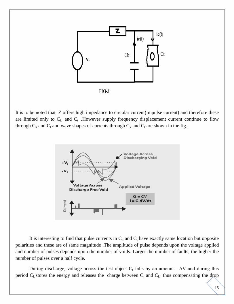
Suppose that the test object remains connected to the voltage source fig-3. Here Ck is the
coupling capacitor. Z is the impedance consisting either only of the lead impedance of or lead
impedance and PD free inductor or filter which decouples the coupling capacitor and the test object
from the source during discharge period only, when very high frequency current pulse i(t) circulate
between Ck and Ct. Ct is the total equipment capacitance of the test specimen.
15
It is to be noted that Z offers high impedance to circular current(impulse current) and therefore these
are limited only to Ck and Ct .However supply frequency displacement current continue to flow
through Ck and Ct and wave shapes of currents through Ck and Ct are shown in the fig.
It is interesting to find that pulse currents in Ck and Ct have exactly same location but opposite
polarities and these are of same magnitude .The amplitude of pulse depends upon the voltage applied
and number of pulses depends upon the number of voids. Larger the number of faults, the higher the
number of pulses over a half cycle.
During discharge, voltage across the test object Ct falls by an amount ∆V and during this
period Ck stores the energy and releases the charge between Ct and Ck thus compensating the drop
Vs
16
∆V . The equivalent capacitance of the test specimen is Ct=Ca+Cb assuming Cc is negligibly small. If
Ck>> Ct then the charge transfer is given by
qc= = (Ca+Cb) ∆V
Now, ΔV ΔVc
ΔV
Therefore, ΔVc
SO, q = Cb ΔVc
If q is known as apparent charge as it is not equal to the charge locally involved Cc∆Vc.This charge q
is more realistic than calculating ∆V, as q is independent of Ca whereas ∆V depends upon Ca.
In practice the condition Ck>> Ct is never satisfied as the Ck will over load the supply and it will be
uneconomical. However Ck is slightly greater than Ct ,the sensitivity of measurement is reduced as
the compensating current ic(t) becomes small. If Ct is comparable to Ck and ∆V is drop in voltage of
Ct the transfer of charge between Ct and Ck result in common voltage ∆V‟.
ΔV‟= = =
∆V‟ is the net rise of voltage of parallel combination of Ck and Ct and therefore the charge qm
transferred to Ct from Ck will be
qm =Ck∆V‟
The charge qm is referred as measurable charge.
=
In order to have high sensitivity of measurement i.e. high qm it is clear that Ck should be large
compared to C=. but we know that there are disadvantage in having high value of Ck. There fore this
method of PD has limited applications.
17
The measurements of PD current pulses provide important information concerning the
discharge processes in a test specimen. The time response of an electric discharge depends mainly on
the nature of fault and design of insulating material. The shape of the circular current is an indication
of the physical discharge process at the fault location in the test object. The principle of measurement
of PD current is shown in the fig.
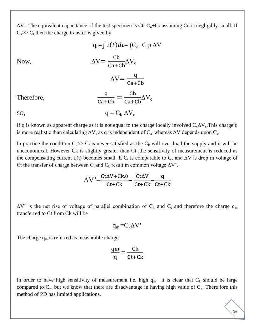
Here C indicates the stray capacitance between the lead of Ct and the earth, the input
capacitance of amplifier and other stray capacitances. The function of high pass amplifier is to
suppress the current iK(t) and Ic(t) and to further amplify the short duration current pulse. The delay
cable is electrically disconnected from R. Suppose during a partial discharge a short duration pulse
current (δt) is produced and results in apparent charge q on Ct which will be redistributed between C,
Ct and Ck. The circuit for the same is given by:
Potential across Ct =

18
Therefore voltage across C will be
V= . = Ct
= =
And because of resistance R the expression for voltage across R will be
V(t) =
R
The voltage across the resistance R indicates a fast rise and is followed by an exponential decay. The
circuit elements have just deferred the original current wave shape especially the wave tail side of the
wave and therefore the measurement of pulse current i(t) is a difficult task.
Also the PD pulse current gets corrupted due to the various
interferences present in the system. The power frequency displacement current ik(t) and it(t) are the

19
major sources of interferences. Higher harmonics in the supply and pulse current in the thyristorised
control circuits are always present which will interfere with the PD currents. On load taps in a
transformer, carbon brushes in generator are yet other sources of noise in the circuits.
Mainly interference can be classified as follows:-
Pulse shaped noise signals: These are due to impulse phenomenon similar to PD currents.
Harmonic signals:- These are mainly due to power supply and thyristorized controller.
We are taking apparent charges as the index level of the partial discharges which is
integration of PD pulse currents. Therefore continuous alternating current of any frequency
would disturb the integration process of measuring circuit and hence it is important that these
currents must be suppressed before the mixture of currents is passed through the integrating
circuits. The solution of the problem is obtained by using filter circuits which may be
completely independent of integrating circuits.
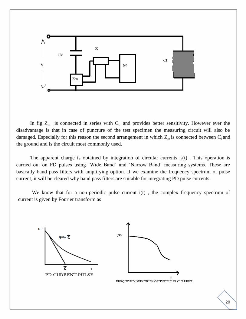
In the following fig. two different ways in which the measuring impedance Zm can be
connected in the circuits.
20
In fig Zm is connected in series with Ct and provides better sensitivity. However ever the
disadvantage is that in case of puncture of the test specimen the measuring circuit will also be
damaged. Especially for this reason the second arrangement in which Zm is connected between Ct and
the ground and is the circuit most commonly used.
The apparent charge is obtained by integration of circular currents ic(t) . This operation is
carried out on PD pulses using „Wide Band‟ and „Narrow Band‟ measuring systems. These are
basically band pass filters with amplifying option. If we examine the frequency spectrum of pulse
current, it will be cleared why band pass filters are suitable for integrating PD pulse currents.
We know that for a non-periodic pulse current i(t) , the complex frequency spectrum of
current is given by Fourier transform as

21
Here the current is approximated by an exponentially decaying curve, neither i(t) not I(jw)
vanish and so a new measure of pulse width required. The time constant is a measure of the width
of i(t) , a line tangent to i(t) , a line tangent to i(t) at t=0 intersects the line i=0 at t= .as shown in
the fig.
From the above expression and fig. it is clear that w 0 I(jw)I0 which means that dc
content of the frequency spectrum equals apparent charge in the pulse current. Therefore the
frequency spectrum of PD pulse current contains complete information concerning the apparent
charge in low frequency range. In order to have proper integration of the pulse current, the time
constant of the pulse should be greater than the time constant of measuring circuit or the band
width (upper cut off frequency) of the measuring system should be much lower than that of spectrum
of pulse currents to be measured.
22
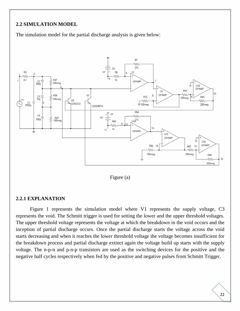
2.2 SIMULATION MODEL
The simulation model for the partial discharge analysis is given below:
Figure (a)
2.2.1 EXPLANATION
Figure 1 represents the simulation model where V1 represents the supply voltage, C3
represents the void. The Schmitt trigger is used for setting the lower and the upper threshold voltages.
The upper threshold voltage represents the voltage at which the breakdown in the void occurs and the
inception of partial discharge occurs. Once the partial discharge starts the voltage across the void
starts decreasing and when it reaches the lower threshold voltage the voltage becomes insufficient for
the breakdown process and partial discharge extinct again the voltage build up starts with the supply
voltage. The n-p-n and p-n-p transistors are used as the switching devices for the positive and the
negative half cycles respectively when fed by the positive and negative pulses from Schmitt Trigger.

23
2.3 PARAMETERS ON WHICH PARTIAL DISCHARGE DEPENDS
The various parameters on which partial discharge depends are:
Supply voltage
Area of the void
Supply frequency
Upper threshold voltage of the Schmitt trigger
Lower threshold voltage of the Schmitt trigger.
2.3.1 PHYSICS BEHIND THE PARTIAL DISCHARGE
Dependence on supply voltage:
The partial discharge patterns are dependent on the magnitude of the supply voltage.
The greater the supply voltage more is the slope and early the partial discharge occurs. And if
the supply voltage is reduced the slope decreases and there is some delay in partial discharge.
Dependence on the supply frequency:
The partial discharge is also dependent on the supply frequency. If we raise the supply
frequency, the rate of change of the voltage becomes high and the partial discharge occurs at
lower voltage.
Dependence on the upper and lower threshold voltage:
The partial discharge patterns are also dependent on the upper threshold voltage and the
lower threshold voltage (of the Schmitt trigger used here). The PD patterns are mainly
dependent on the difference of the upper and the lower threshold voltage as the charge
transfer is dependent on the difference:
Q α (VUT-VLT)
More is the difference between VUT and VLT more early the PD occurs. If we fix the
VUT and start increasing the VLT the PD starts at higher voltage and vice versa. Same case
occurs when we fix the VLT and start decreasing VUT.
24
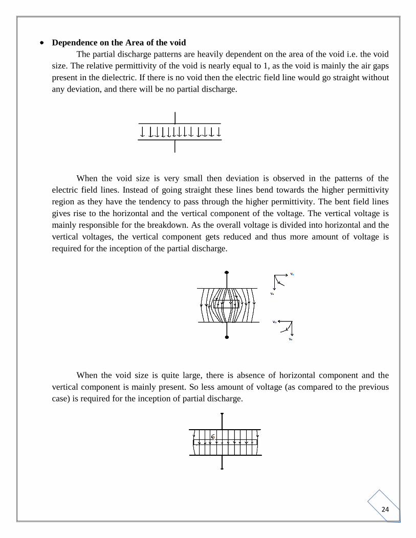
Dependence on the Area of the void
The partial discharge patterns are heavily dependent on the area of the void i.e. the void
size. The relative permittivity of the void is nearly equal to 1, as the void is mainly the air gaps
present in the dielectric. If there is no void then the electric field line would go straight without
any deviation, and there will be no partial discharge.
When the void size is very small then deviation is observed in the patterns of the
electric field lines. Instead of going straight these lines bend towards the higher permittivity
region as they have the tendency to pass through the higher permittivity. The bent field lines
gives rise to the horizontal and the vertical component of the voltage. The vertical voltage is
mainly responsible for the breakdown. As the overall voltage is divided into horizontal and the
vertical voltages, the vertical component gets reduced and thus more amount of voltage is
required for the inception of the partial discharge.
When the void size is quite large, there is absence of horizontal component and the
vertical component is mainly present. So less amount of voltage (as compared to the previous
case) is required for the inception of partial discharge.
25
CHAPTER 3
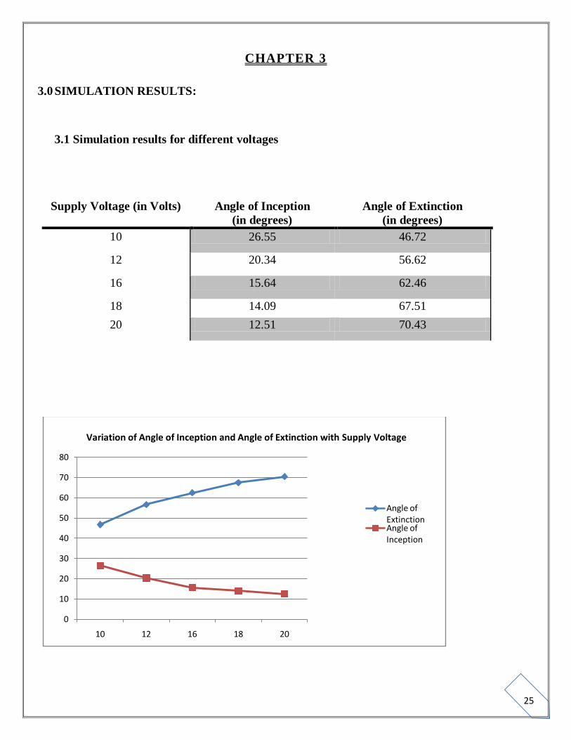
3.0 SIMULATION RESULTS:
3.1 Simulation results for different voltages
Supply Voltage (in Volts) Angle of Inception
(in degrees)
Angle of Extinction
(in degrees)
10 26.55 46.72
12 20.34 56.62
16 15.64 62.46
18 14.09 67.51
20 12.51 70.43
0
10
20
30
40
50
60
70
80
10 12 16 18 20
Angle of ExtinctionAngle of Inception
Variation of Angle of Inception and Angle of Extinction with Supply Voltage
26
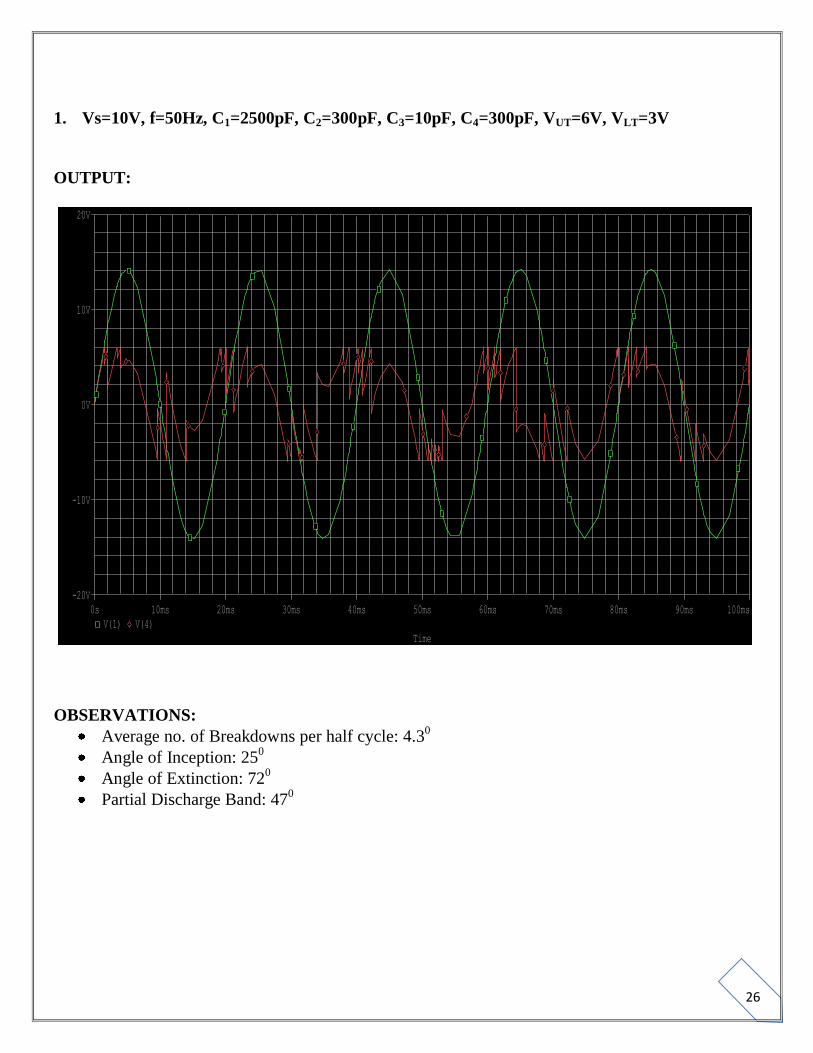
1. Vs=10V, f=50Hz, C1=2500pF, C2=300pF, C3=10pF, C4=300pF, VUT=6V, VLT=3V
OUTPUT:
OBSERVATIONS:
Average no. of Breakdowns per half cycle: 4.30
Angle of Inception: 250
Angle of Extinction: 720
Partial Discharge Band: 470
Time
0s 10ms 20ms 30ms 40ms 50ms 60ms 70ms 80ms 90ms 100ms
V(1) V(4)
-20V
-10V
0V
10V
20V

27
2. Vs=12V, C1=2500pF, C2=300pF, C3=10pF, C4=300pF, VUT=6V, VLT=3V
OUTPUT:
OBSERVATIONS:
Average no. of Breakdowns per half cycle: 5
Angle of Inception: 20.340
Angle of Extinction: 79.830
Partial Discharge Band: 59.490
Time
0s 10ms 20ms 30ms 40ms 50ms 60ms 70ms 80ms 90ms 100ms
V(1) V(4)
-20V
-10V
0V
10V
20V
28
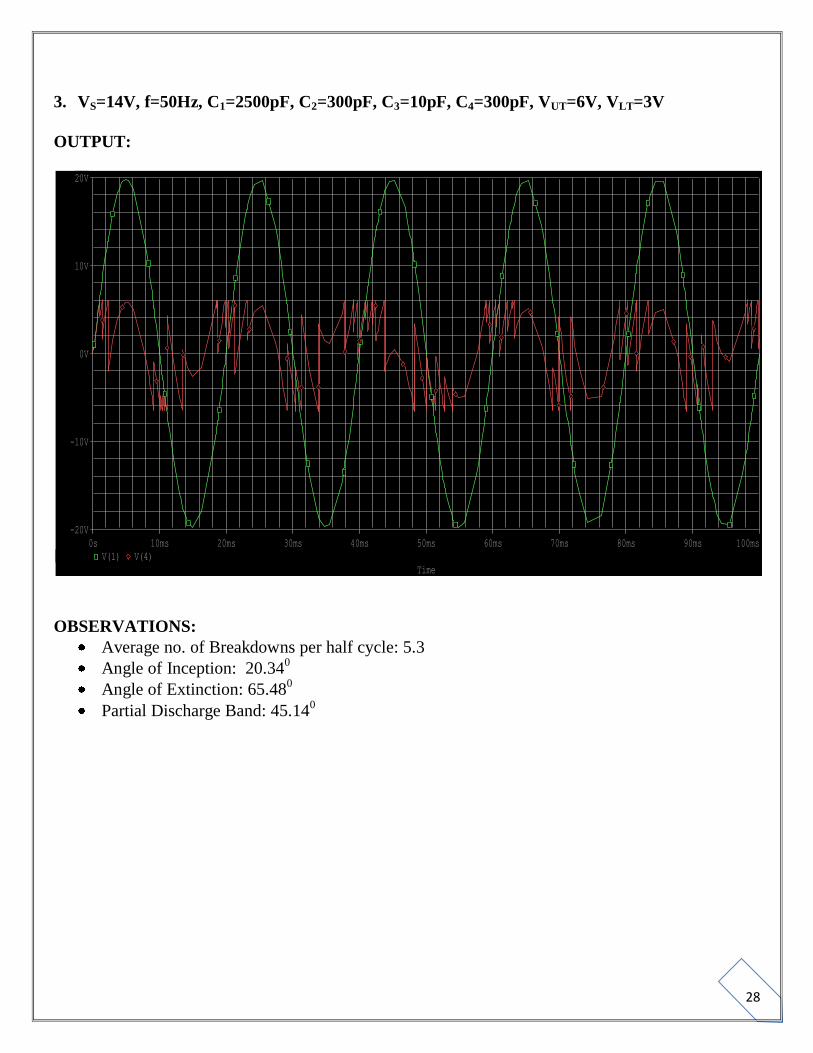
3. VS=14V, f=50Hz, C1=2500pF, C2=300pF, C3=10pF, C4=300pF, VUT=6V, VLT=3V
OUTPUT:
OBSERVATIONS:
Average no. of Breakdowns per half cycle: 5.3
Angle of Inception: 20.340
Angle of Extinction: 65.480
Partial Discharge Band: 45.140
Time
0s 10ms 20ms 30ms 40ms 50ms 60ms 70ms 80ms 90ms 100ms
V(1) V(4)
-20V
-10V
0V
10V
20V
29
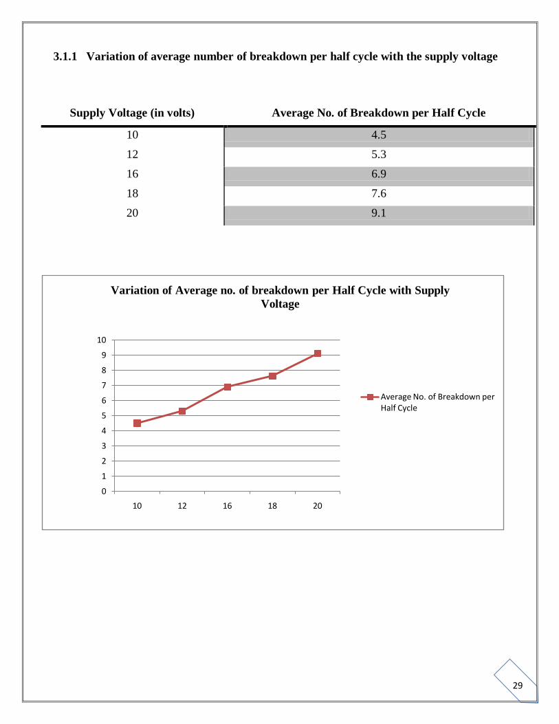
3.1.1 Variation of average number of breakdown per half cycle with the supply voltage
Supply Voltage (in volts) Average No. of Breakdown per Half Cycle
10 4.5
12 5.3
16 6.9
18 7.6
20 9.1
0
1
2
3
4
5
6
7
8
9
10
10 12 16 18 20
Average No. of Breakdown per Half Cycle
Variation of Average no. of breakdown per Half Cycle with Supply
Voltage
30
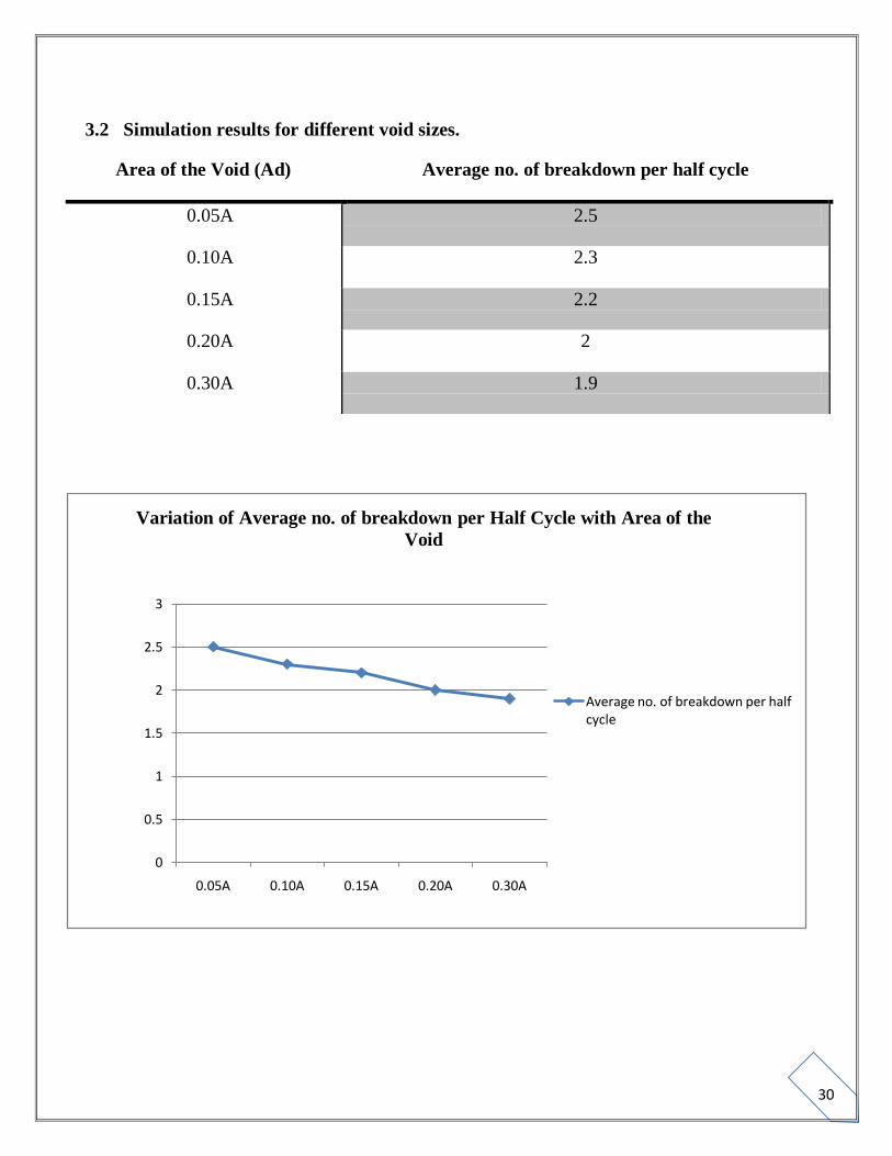
3.2 Simulation results for different void sizes.
Area of the Void (Ad) Average no. of breakdown per half cycle
0.05A 2.5
0.10A 2.3
0.15A 2.2
0.20A 2
0.30A 1.9
0
0.5
1
1.5
2
2.5
3
0.05A 0.10A 0.15A 0.20A 0.30A
Average no. of breakdown per half cycle
Variation of Average no. of breakdown per Half Cycle with Area of the
Void

31
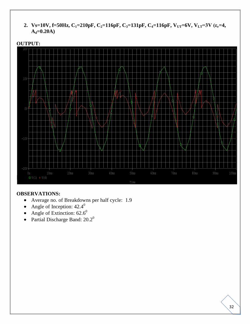
1. Vs=10V, f=50Hz, C1=210pF, C2=115pF, C3=170pF, C4=115pF, VUT=6V, VLT=3V (εr=3,
Ad=0.20A)
OUTPUT:
OBSERVATIONS:
Average no. of Breakdowns per half cycle: 1.7
Angle of Inception: 43.830
Angle of Extinction: 51.460
Partial Discharge Band: 7.630
Time
0s 10ms 20ms 30ms 40ms 50ms 60ms 70ms 80ms 90ms 100ms
V(1) V(4)
-20V
-10V
0V
10V
20V
32
2. Vs=10V, f=50Hz, C1=210pF, C2=116pF, C3=131pF, C4=116pF, VUT=6V, VLT=3V (εr=4,
Ad=0.20A)
OUTPUT:
OBSERVATIONS:
Average no. of Breakdowns per half cycle: 1.9
Angle of Inception: 42.40
Angle of Extinction: 62.60
Partial Discharge Band: 20.20
Time
0s 10ms 20ms 30ms 40ms 50ms 60ms 70ms 80ms 90ms 100ms
V(1) V(4)
-20V
-10V
0V
10V
20V

33
3. Vs=10V, f=50Hz, C1=100pF, C2=100pF, C3=145pF, C4=100pF, VUT=6V, VLT=3V (εr=3,
Ad=0.30A)
OUTPUT:
OBSERVATIONS:
Average no. of Breakdowns per half cycle: 1.4
Angle of Inception: 23.340
Angle of Extinction: 61.050
Partial Discharge Band: 37.710
Time
0s 10ms 20ms 30ms 40ms 50ms 60ms 70ms 80ms 90ms 100ms
V(1) V(4)
-20V
-10V
0V
10V
20V

34
4. Vs=10V, f=50Hz, C1=190pF, C2=180pF, C3=200pF, C4=180pF, VUT=6V, VLT=3V (εr=4,
Ad=0.30A)
OUTPUT:
OBSERVATIONS:
Average no. of Breakdowns per half cycle: 2.3
Angle of Inception: 39.130
Angle of Extinction: 53.220
Partial Discharge Band: 14.090
Time
0s 10ms 20ms 30ms 40ms 50ms 60ms 70ms 80ms 90ms 100ms
V(1) V(4)
-20V
-10V
0V
10V
20V
35
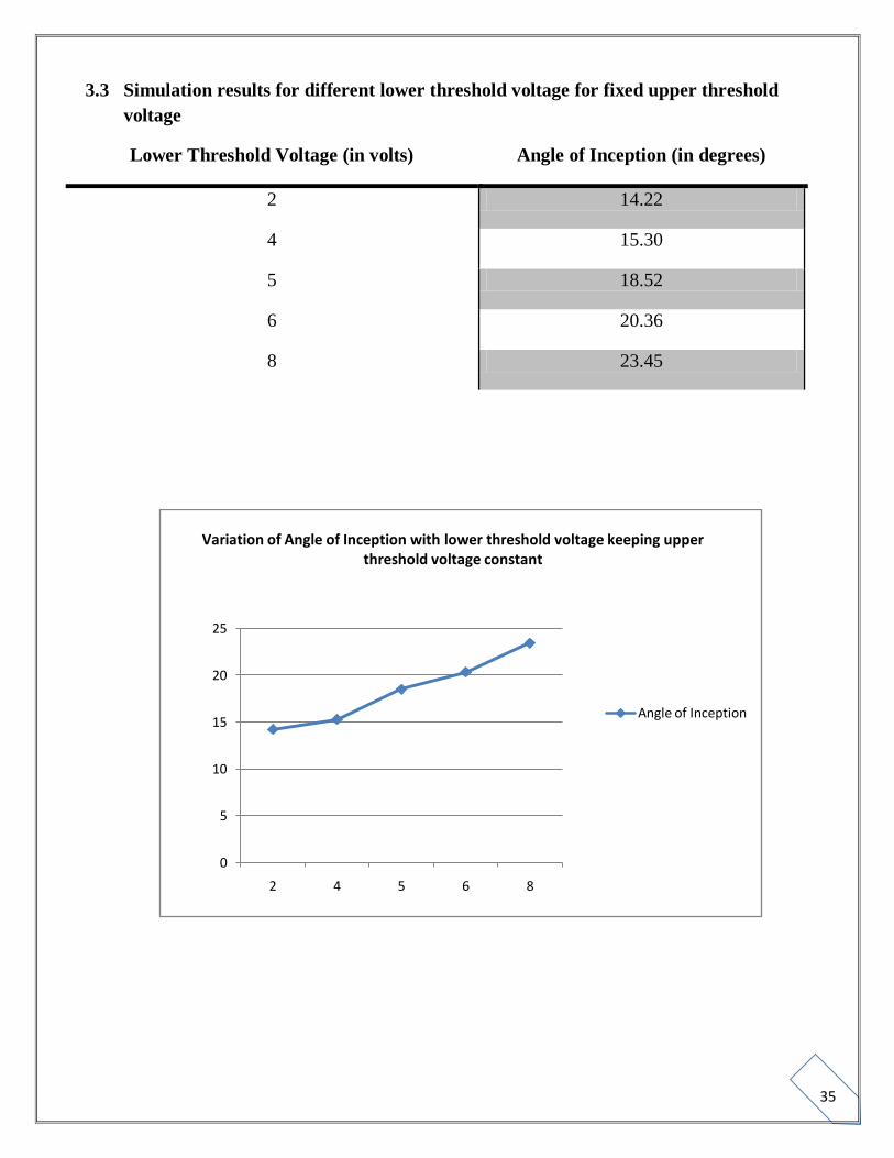
3.3 Simulation results for different lower threshold voltage for fixed upper threshold
voltage
Lower Threshold Voltage (in volts) Angle of Inception (in degrees)
2 14.22
4 15.30
5 18.52
6 20.36
8 23.45
0
5
10
15
20
25
2 4 5 6 8
Angle of Inception
Variation of Angle of Inception with lower threshold voltage keeping upper threshold voltage constant
36
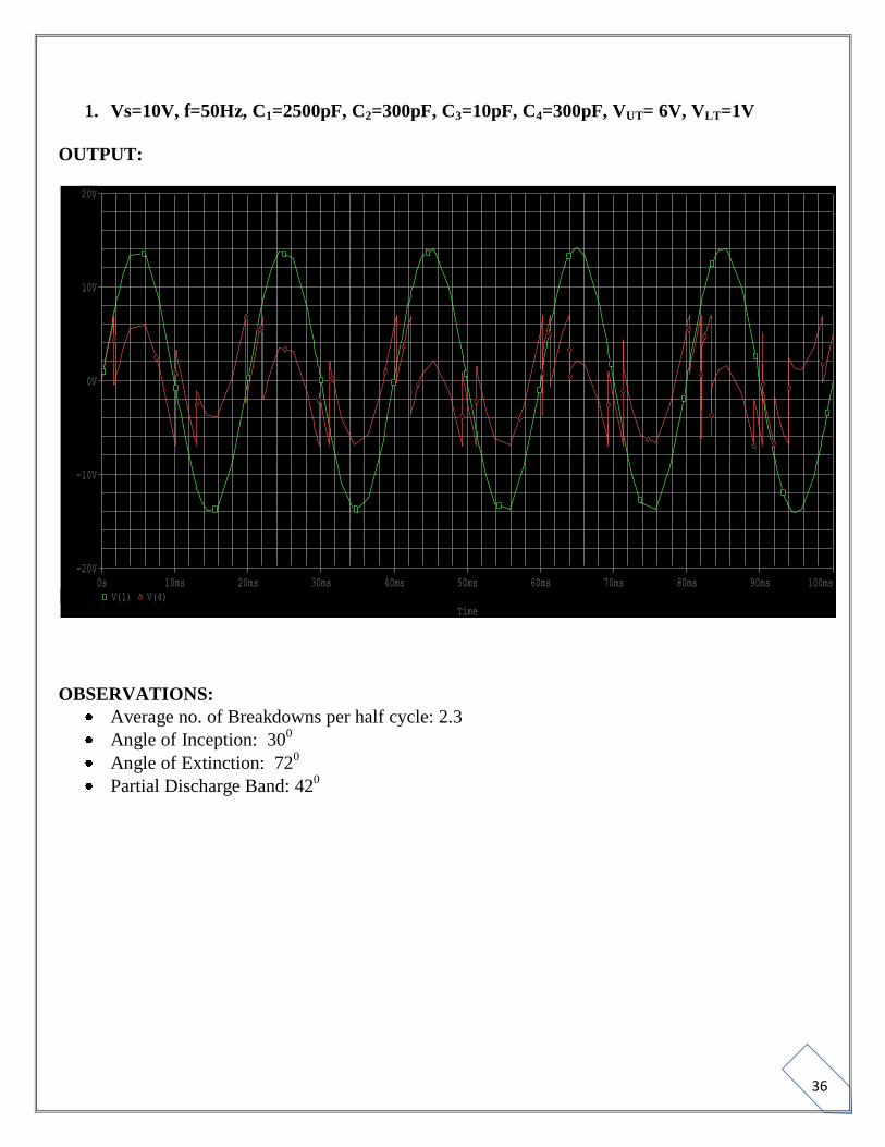
1. Vs=10V, f=50Hz, C1=2500pF, C2=300pF, C3=10pF, C4=300pF, VUT= 6V, VLT=1V
OUTPUT:
OBSERVATIONS:
Average no. of Breakdowns per half cycle: 2.3
Angle of Inception: 300
Angle of Extinction: 720
Partial Discharge Band: 420
Time
0s 10ms 20ms 30ms 40ms 50ms 60ms 70ms 80ms 90ms 100ms
V(1) V(4)
-20V
-10V
0V
10V
20V

37
2. Vs=10V, f=50Hz, C1=2500pF, C2=300pF, C3=10pF, C4=300pF, VUT= 6V, VLT=2V
OUTPUT:
OBSERVATIONS:
Average no. of Breakdowns per half cycle: 2.8
Angle of Inception: 280
Angle of Extinction: 68.40
Partial Discharge Band: 40.40
Time
0s 10ms 20ms 30ms 40ms 50ms 60ms 70ms 80ms 90ms 100ms
V(1) V(4)
-20V
-10V
0V
10V
20V
38
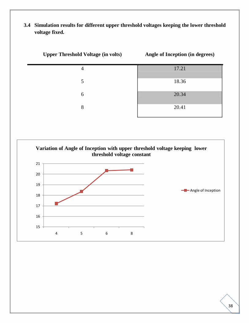
3.4 Simulation results for different upper threshold voltages keeping the lower threshold
voltage fixed.
Upper Threshold Voltage (in volts) Angle of Inception (in degrees)
4 17.21
5 18.36
6 20.34
8 20.41
15
16
17
18
19
20
21
4 5 6 8
Angle of Inception
Variation of Angle of Inception with upper threshold voltage keeping lower
threshold voltage constant

39
1. Vs=10V, f=50Hz, C1=2500pF, C2=300pF, C3=10pF, C4=300pF, VUT=5V, VLT=2V
OUTPUT:
OBSERVATIONS:
Average no. of Breakdowns per half cycle: 4.0
Angle of Inception: 24.80
Angle of Extinction: 540
Partial Discharge Band: 29.20
Time
0s 10ms 20ms 30ms 40ms 50ms 60ms 70ms 80ms 90ms 100ms
V(1) V(4)
-20V
-10V
0V
10V
20V

40
2. Vs=10V, f=50Hz, C1=2500pF, C2=300pF, C3=10pF, C4=300pF, VUT=7V, VLT=2V
OUTPUT:
OBSERVATIONS:
Average no. of Breakdowns per half cycle: 2.6
Angle of Inception: 31.320
Angle of Extinction: 60.960
Partial Discharge Band: 29.640
Time
0s 10ms 20ms 30ms 40ms 50ms 60ms 70ms 80ms 90ms 100ms
V(1) V(4)
-20V
-10V
0V
10V
20V

41
3.5 Simulation results for different values of permittivity
1. Vs=10V, f=50Hz, C1=230pF, C2=55pF, C3=85pF, C4=55pF, VUT=6V, VLT=3V, εr=3
OUTPUT:
OBSERVATIONS:
Average no. of Breakdowns per half cycle: 1.2
Angle of Inception: 360
Angle of Extinction: 67.50
Partial Discharge Band: 31.50
Time
0s 10ms 20ms 30ms 40ms 50ms 60ms 70ms 80ms 90ms 100ms
V(1) V(4)
-20V
-10V
0V
10V
20V
42
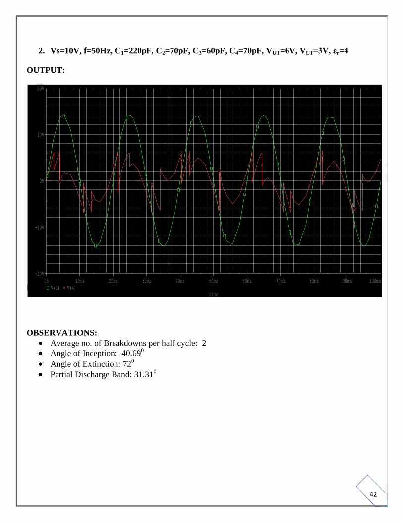
2. Vs=10V, f=50Hz, C1=220pF, C2=70pF, C3=60pF, C4=70pF, VUT=6V, VLT=3V, εr=4
OUTPUT:
OBSERVATIONS:
Average no. of Breakdowns per half cycle: 2
Angle of Inception: 40.690
Angle of Extinction: 720
Partial Discharge Band: 31.310
Time
0s 10ms 20ms 30ms 40ms 50ms 60ms 70ms 80ms 90ms 100ms
V(1) V(4)
-20V
-10V
0V
10V
20V
43
3.6 Simulation results for different values of frequency
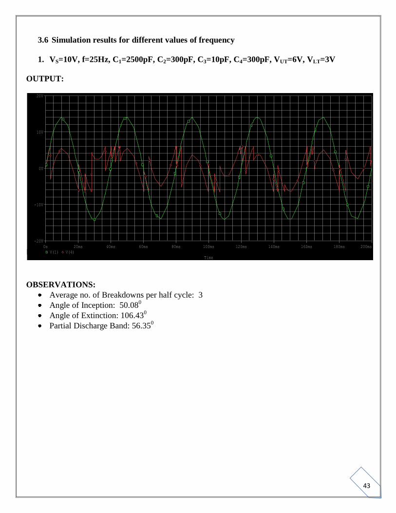
1. VS=10V, f=25Hz, C1=2500pF, C2=300pF, C3=10pF, C4=300pF, VUT=6V, VLT=3V
OUTPUT:
OBSERVATIONS:
Average no. of Breakdowns per half cycle: 3
Angle of Inception: 50.080
Angle of Extinction: 106.430
Partial Discharge Band: 56.350
Time
0s 20ms 40ms 60ms 80ms 100ms 120ms 140ms 160ms 180ms 200ms
V(1) V(4)
-20V
-10V
0V
10V
20V
44
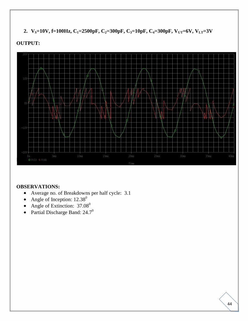
2. VS=10V, f=100Hz, C1=2500pF, C2=300pF, C3=10pF, C4=300pF, VUT=6V, VLT=3V
OUTPUT:
OBSERVATIONS:
Average no. of Breakdowns per half cycle: 3.1
Angle of Inception: 12.380
Angle of Extinction: 37.080
Partial Discharge Band: 24.70
Time
0s 5ms 10ms 15ms 20ms 25ms 30ms 35ms 40ms
V(1) V(4)
-20V
-10V
0V
10V
20V

45
3. VS=10V, f=200Hz, C1=2500pF, C2=300pF, C3=10pF, C4=300pF, VUT=6V, VLT=3V
OUTPUT:
OBSERVATIONS:
Average no. of Breakdowns per half cycle: 3.6
Angle of Inception: 6.370
Angle of Extinction:11.070
Partial Discharge Band: 4.70
Time
0s 2ms 4ms 6ms 8ms 10ms 12ms 14ms 16ms
V(1) V(4)
-20V
-10V
0V
10V
20V
46
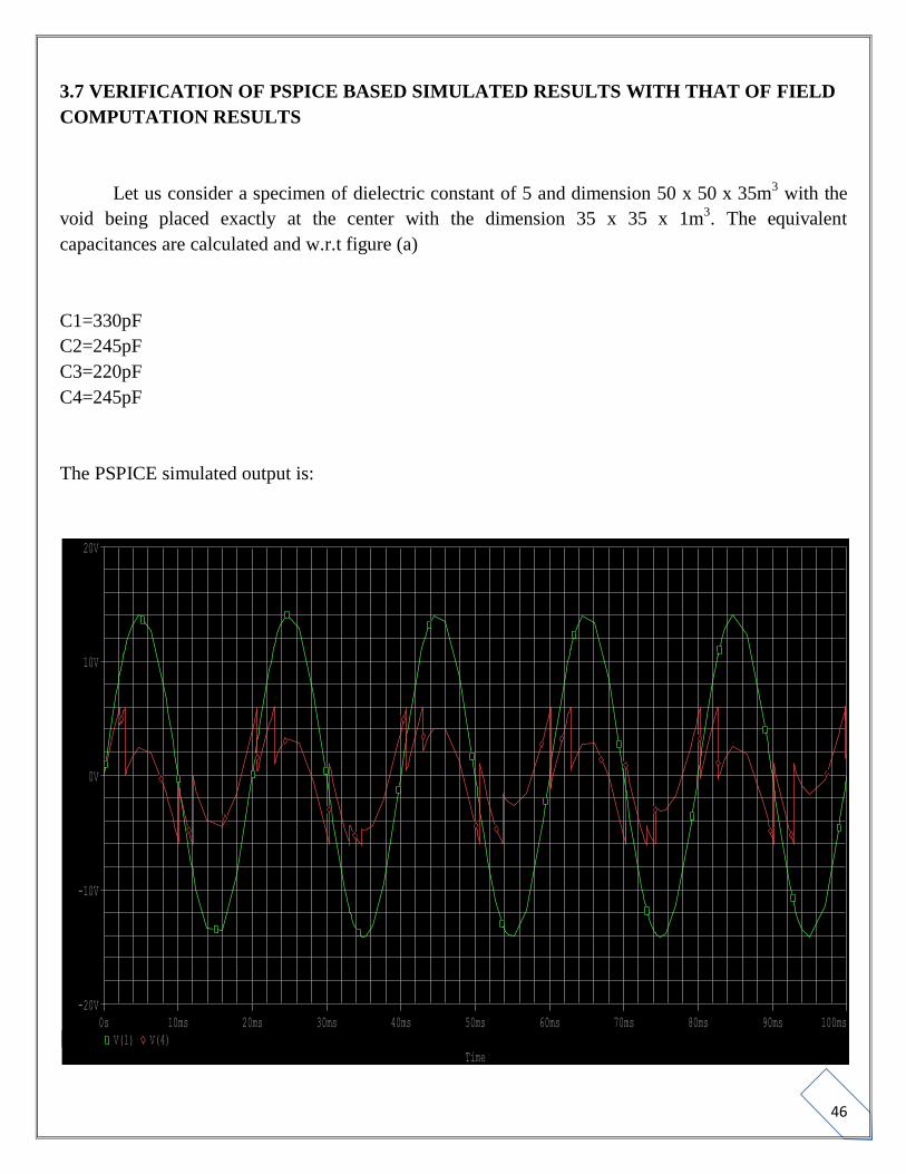
3.7 VERIFICATION OF PSPICE BASED SIMULATED RESULTS WITH THAT OF FIELD
COMPUTATION RESULTS
Let us consider a specimen of dielectric constant of 5 and dimension 50 x 50 x 35m3 with the
void being placed exactly at the center with the dimension 35 x 35 x 1m3. The equivalent
capacitances are calculated and w.r.t figure (a)
C1=330pF
C2=245pF
C3=220pF
C4=245pF
The PSPICE simulated output is:
Time
0s 10ms 20ms 30ms 40ms 50ms 60ms 70ms 80ms 90ms 100ms
V(1) V(4)
-20V
-10V
0V
10V
20V

47
The results obtained by this particular method have been compared with the results obtained from a
C++ program, which is based on field computation results. In a C++ program language following
parameters are considered-
Critical voltage for discharge inception
Residual voltage for discharge extinction
Critical voltage for discharge propagation
Size of the void
Location of the void within dielectric
The results are compared in terms of angle of inception obtained. It can be seen from the table:
Angle of inception by PSPICE (in
degree)
Angle of inception by C++
The results obtained are quite close which validates the model in particular sense.

48
CHAPTER 4
4.1 CONCLUSION
From the above simulation model we see that the partial discharge largely depends on the supply
voltage, supply frequency, size of the void, upper threshold voltage and the lower threshold
voltage.
From the observations we see that with the increase of supply voltage the angle of inception
decreases as the slope of the voltage profile is increased and the PD occurs earlier. Also the
average numbers of breakdown rises i.e. the more amount of PD patterns are observed.
Increase of supply frequency causes more rate of change of voltage profile so the PD patterns
occur earlier. Also the average number of breakdown per half cycle increases.
As the size of the void is small, more amount of voltage is needed for inception of PD patterns as
the voltage gets divided into horizontal and vertical components and the vertical components are
responsible for the breakdown. So as the void size increases the horizontal component of the
voltage decreases and the vertical component increases so PD patterns starts early.
As the upper threshold voltage rises, the PD patterns starts later as more time is required to reach
that high voltage. And PD patterns start earlier when the upper threshold voltage is lower.
The PD patterns depend on the difference between the upper threshold voltage and the lower
threshold voltage. So as the lower threshold voltage is increased keeping the upper threshold
voltage fixed, the PD pattern starts later and vice versa.
4.2 FUTURE SCOPE
Here only the PSPICE simulated model is represented. The hardware model can be made and
compared with the simulated model.
To simulate partial discharge patterns for multiple voids, spherical voids and cylindrical voids.
The angle of extinction can be matched with the C++ language.

49
4.3 REFERENCES
SPICE: Users guide and reference, edition 1.3 by Michael B. Steer
High Voltage Engineering by C.L. Wadha
Partial Discharge theory and applications to electrical equipment by Gabe Paoletti
Investigation of the Voltage Influence on Partial Discharge Characteristic Parameters in
Solid Insulation by P. Valatka, V. Sučila
High-voltage test techniques – Partial discharge measurements