Pages SPI Nand flash controller Application Note for 1Gb/2Gb … Application N… · Resume 7Ah X...
31
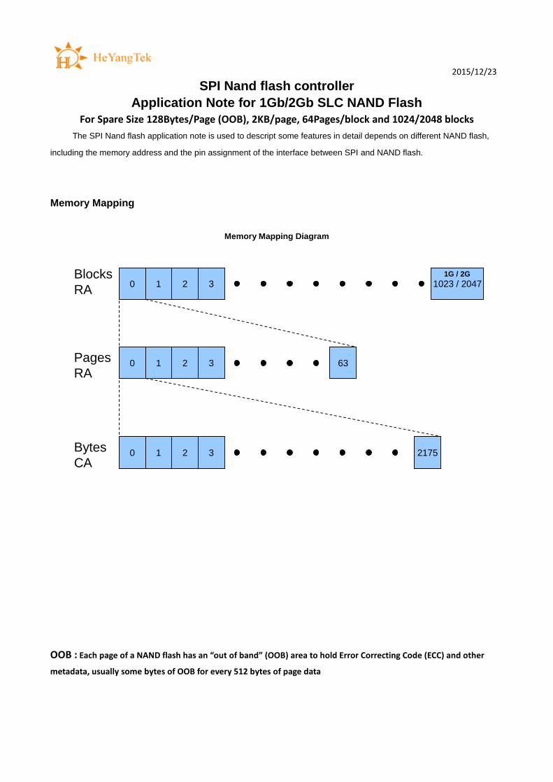
2015/12/23 SPI Nand flash controller Application Note for 1Gb/2Gb SLC NAND Flash For Spare Size 128Bytes/Page (OOB), 2KB/page, 64Pages/block and 1024/2048 blocks The SPI Nand flash application note is used to descript some features in detail depends on different NAND flash, including the memory address and the pin assignment of the interface between SPI and NAND flash. Memory Mapping Memory Mapping Diagram OOB : Each page of a NAND flash has an “out of band” (OOB) area to hold Error Correcting Code (ECC) and other metadata, usually some bytes of OOB for every 512 bytes of page data 0 1 2 3 1023 / 2047 0 1 2 3 63 0 1 2 3 2175 Blocks RA Pages RA Bytes CA 1G / 2G
Transcript of Pages SPI Nand flash controller Application Note for 1Gb/2Gb … Application N… · Resume 7Ah X...
2015/12/23
SPI Nand flash controller
Application Note for 1Gb/2Gb SLC NAND Flash
For Spare Size 128Bytes/Page (OOB), 2KB/page, 64Pages/block and 1024/2048 blocks
The SPI Nand flash application note is used to descript some features in detail depends on different NAND flash,
including the memory address and the pin assignment of the interface between SPI and NAND flash.
Memory Mapping
Memory Mapping Diagram
OOB : Each page of a NAND flash has an “out of band” (OOB) area to hold Error Correcting Code (ECC) and other
metadata, usually some bytes of OOB for every 512 bytes of page data
0 1 2 3 1023 / 2047
0 1 2 3 63
0 1 2 3 2175
Blocks
RA
Pages
RA
Bytes
CA
1G / 2G

2015/12/23
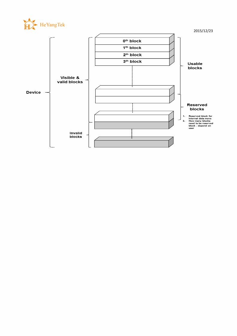
Application Note – A : Invalid blocks (bad blocks)
The device of SPI Nand flash occasionally contains invalid blocks, Therefore, user need find invalid block
out and manage these invalid blocks.
2048B 128BBlock
1 page (program unit) = (2K+128) bytes
1 block (Erase unit) = (2K+128)*64 pages = (128K+8K) bytes
1 G device = (128K+8K)*1024 blocks = (128MB+8MB)
or
2 G device = (128K+8K)*2048 blocks = (256MB+16MB)
Device
Page1 G: 1024 Blocks
2 G: 2048 Blocks
64 Pages
2015/12/23
2015/12/23
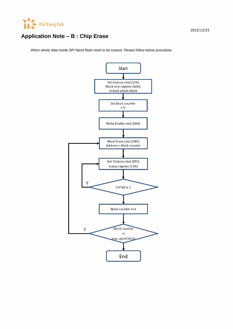
Application Note – B : Chip Erase
When whole data inside SPI Nand flash need to be erased. Please follow below procedure.

2015/12/23
Application Note – C : Program after erase
In SPI Nand flash, the block is the min. erase unit so users want to program data to SPI Nand flash.

2015/12/23
Application Note – D : Read Data

2015/12/23
Application Note – E : Internal Data Move without Updated Data

2015/12/23
Application Note – F : Internal Data Move with Updated Data

2015/12/23
Application Note – G : Update new data into used block of SPI Nand flash
Users want to update new data into a block of SPI Nand flash which has been programmed before. The
below flow has to be followed.
If the xth page and (x+1) page of yth block will to be updated

2015/12/23

2015/12/23
Application Note – H :
IF page size = 2KB and spare size = 128B and ECC : 14 bits/512B
Then page data format as below
2KB/Page and ECC
System
Partition
Block
Page0
Page1
Page62
Page63
Byte0
~
byte511
Byte512
~
byte1023
Byte1536
~
Byte2047
Byte2048 ~ Byte2079
Byte2080 ~ Byte2111
Byte2144 ~ Byte2175Don’t care
Byte0
Byte1
Byte2
Byte3
Byte4
Byte5
Byte6
Byte7
Don’t care
(4 bytes)
Logic block address
(2 bytes)
Version of code
(2 bytes)
Don’t care
(24 bytes)
Page Size Spare Size ECC Cap User Data Meta Data ECC Data Unprotected Data
2048 Bytes 128 Bytes
0 Bit 512 Bytes x4 32 Bytes x4 0 --
2 Bits 512 Bytes x4 28 Bytes x4 4 Bytes x4
1st to 4th byte in meta data
are unprotected by ECC.
4 Bits 512 Bytes x4 24 Bytes x4 8 Bytes x4
6 Bits 512 Bytes x4 22 Bytes x4 10 Bytes x4
8 Bits 512 Bytes x4 18 Bytes x4 14 Bytes x4
14 Bits 512 Bytes x4 8 Bytes x4 24 Bytes x4
Default ECC : 14bits/512B

2015/12/23
Application Note – I : Partition and User area (1)
2015/12/23
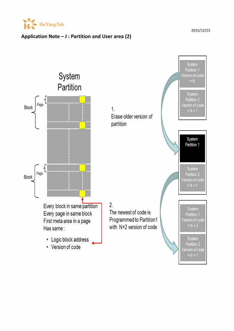
Application Note – J : Partition and User area (2)
2015/12/23
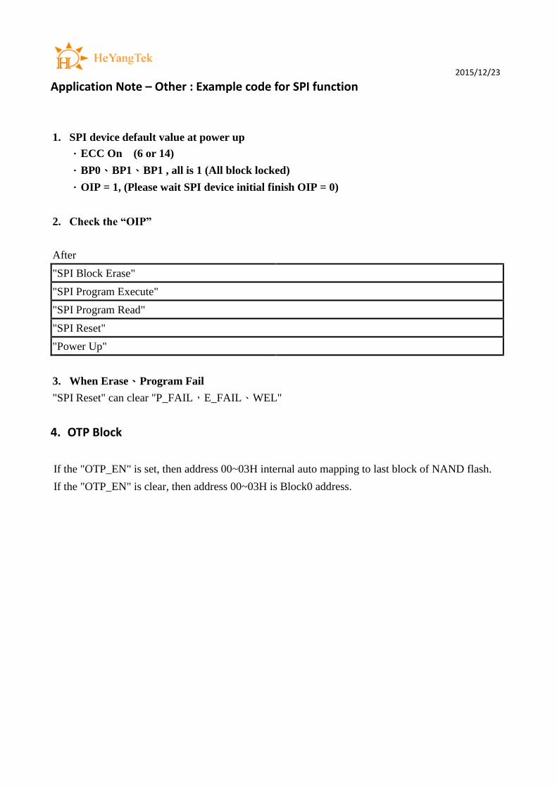
Application Note – Other : Example code for SPI function
1. SPI device default value at power up
.ECC On (6 or 14)
.BP0、BP1、BP1 , all is 1 (All block locked)
.OIP = 1, (Please wait SPI device initial finish OIP = 0)
2. Check the “OIP”
After
"SPI Block Erase"
"SPI Program Execute"
"SPI Program Read"
"SPI Reset"
"Power Up"
3. When Erase、Program Fail
"SPI Reset" can clear "P_FAIL,E_FAIL、WEL"
4. OTP Block
If the "OTP_EN" is set, then address 00~03H internal auto mapping to last block of NAND flash.
If the "OTP_EN" is clear, then address 00~03H is Block0 address.

2015/12/23
Application Note – Other : Example code for SPI function
Note: The content code is similar to C code , but not real C code.
Address : The address is comprised of a column address with 2 bytes and a row address with 3 bytes.
The "row address" identifies the page, block.
The "column address" identifies the byte within a page to access.
//----------------------------------------------------------------------------------------------------------------------------- ---
#define SPI_CS //SPI device Chip Select ( 0:Active 1:Inactive)
#define SPI_SI //(8 bit register) Host send data to SPI device
#define SPI_SO //(8 bit register) Host received data from SPI device
#define NOP //Nothing, if need waiting for Host SPI active.
//Address transform to Row Address
//Define SPI NAND Flash : Block 512, Page 128
//Data Type declaration
unsigned long Row_Address;
unsigned long Column_Address;
unsigned char xStatusReg;
unsigned char xDataBuffer[2048];
//Block & Page number transform to NAND flash address//
//Note: Except Column address.
void AddressTrans(unsigned long Block, unsigned int Page)
{
Row_Address = (Block<<6)|Page; //Base on 64 pages.
}
2015/12/23
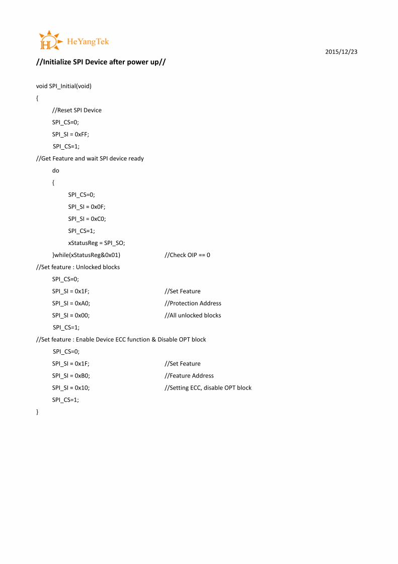
//Initialize SPI Device after power up//
void SPI_Initial(void)
{
//Reset SPI Device
SPI_CS=0;
SPI_SI = 0xFF;
SPI_CS=1;
//Get Feature and wait SPI device ready
do
{
SPI_CS=0;
SPI_SI = 0x0F;
SPI_SI = 0xC0;
SPI_CS=1;
xStatusReg = SPI_SO;
}while(xStatusReg&0x01) //Check OIP == 0
//Set feature : Unlocked blocks
SPI_CS=0;
SPI_SI = 0x1F; //Set Feature
SPI_SI = 0xA0; //Protection Address
SPI_SI = 0x00; //All unlocked blocks
SPI_CS=1;
//Set feature : Enable Device ECC function & Disable OPT block
SPI_CS=0;
SPI_SI = 0x1F; //Set Feature
SPI_SI = 0xB0; //Feature Address
SPI_SI = 0x10; //Setting ECC, disable OPT block
SPI_CS=1;
}

2015/12/23
//SPI Erase function//
unsigned int SPI_Erase(unsigned int Block)
{
Row_Address = AddressTrans(Block, 0);
//Write Enable
SPI_CS=0;
SPI_SI = 0x06; //Write Enable Command
SPI_CS=1;
//Erase and Block Address
SPI_CS=0;
SPI_SI = 0xD8; //Erase Command
SPI_SI = Row_Address>>16; //A23~A16
SPI_SI = Row_Address>>8; //A15~A8;
SPI_SI = Row_Address; //A7~A0;
SPI_CS=1;
//Get Feature and wait SPI device ready
do
{
SPI_CS=0;
SPI_SI = 0x0F;
SPI_SI = 0xC0;
SPI_CS=1;
xStatusReg = SPI_SO;
}while(xStatusReg&0x01)
return ((xStatusReg>>2)&0x01); //return Erase Success = 0, or Fail = 1;
}

2015/12/23
//SPI Program function//
unsigned int SPI_Program(unsigned int Block, unsigned int Page)
{
Row_Address = AddressTrans(Block, Page);
//Write Enable
SPI_CS=0;
SPI_SI = 0x06; //Write Enable
SPI_CS=1;
//Data Load to SPI device cache buffer
SPI_CS=0;
SPI_SI = 0x02; //Program Load
SPI_SI = Column_Address>>8; //A15~A8;
SPI_SI = Column_Address; //A7~A0;
//Host send Data to SPI device
for(int i=0;i<2048;i++)
{
SPI_SI = xDataBuffer[i];
}
SPI_CS=1;
//Execute Program
SPI_CS=0;
SPI_SI = 0x10; //Program Execute
SPI_SI = Row_Address>>16; //A23~A16
SPI_SI = Row_Address>>8; //A15~A8;
SPI_SI = Row_Address; //A7~A0;
SPI_CS=1;
//Get Feature and wait SPI device ready
do
{
SPI_CS=0;
SPI_SI = 0x0F; //Get Feature
SPI_SI = 0xC0; //Status Address
SPI_CS=1;
xStatusReg = SPI_SO;
}while(xStatusReg&0x01)
return ((xStatusReg>>3)&0x01); //return Program Success = 0, or Fail = 1;
}

2015/12/23
//SPI Read function//
void SPI_Read(unsigned int Block, unsigned int Page)
{
Row_Address = AddressTrans(Block, Page);
//Read Page data to SPI device catch buffer
SPI_CS=0;
SPI_SI = 0x13; //Page Read (to Cache)
SPI_SI = Row_Address>>16; //A23~A16
SPI_SI = Row_Address>>8; //A15~A8;
SPI_SI = Row_Address; //A7~A0;
SPI_CS=1;
//Get Feature and wait SPI device ready
do
{
SPI_CS=0;
SPI_SI = 0x0F; //Get Feature
SPI_SI = 0xC0; //Status Address
SPI_CS=1;
xStatusReg = SPI_SO;
}while(xStatusReg&0x01)
//Read Data form SPI device cache buffer
SPI_CS=0;
SPI_SI = 0x03; //Read from Cache
SPI_SI = Column_Address>>8; //A15~A8;
SPI_SI = Column_Address; //A7~A0;
SPI_SI = 0x00 //Dummy Byte;
//Host received data from SPI device
for(int i=0;i<2048;i++)
{
xDataBuffer[i] = SPI_SO;
}
SPI_CS=1;
}
2015/12/23
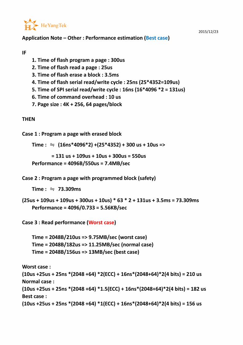
Application Note – Other : Performance estimation (Best case)
IF
1. Time of flash program a page : 300us
2. Time of flash read a page : 25us
3. Time of flash erase a block : 3.5ms
4. Time of flash serial read/write cycle : 25ns (25*4352=109us)
5. Time of SPI serial read/write cycle : 16ns (16*4096 *2 = 131us)
6. Time of command overhead : 10 us
7. Page size : 4K + 256, 64 pages/block
THEN
Case 1 : Program a page with erased block
Time : ≒ (16ns*4096*2) +(25*4352) + 300 us + 10us =>
= 131 us + 109us + 10us + 300us = 550us
Performance = 4096B/550us = 7.4MB/sec
Case 2 : Program a page with programmed block (safety)
Time : ≒ 73.309ms
(25us + 109us + 109us + 300us + 10us) * 63 * 2 + 131us + 3.5ms = 73.309ms
Performance = 4096/0.733 = 5.56KB/sec
Case 3 : Read performance (Worst case)
Time = 2048B/210us => 9.75MB/sec (worst case)
Time = 2048B/182us => 11.25MB/sec (normal case)
Time = 2048B/156us => 13MB/sec (best case)
Worst case :
(10us +25us + 25ns *(2048 +64) *2(ECC) + 16ns*(2048+64)*2(4 bits) = 210 us
Normal case :
(10us +25us + 25ns *(2048 +64) *1.5(ECC) + 16ns*(2048+64)*2(4 bits) = 182 us
Best case :
(10us +25us + 25ns *(2048 +64) *1(ECC) + 16ns*(2048+64)*2(4 bits) = 156 us
2015/12/23
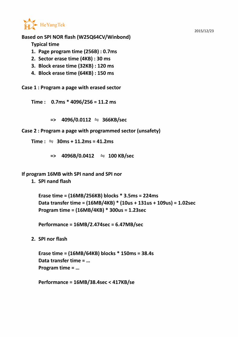
Based on SPI NOR flash (W25Q64CV/Winbond)
Typical time
1. Page program time (256B) : 0.7ms
2. Sector erase time (4KB) : 30 ms
3. Block erase time (32KB) : 120 ms
4. Block erase time (64KB) : 150 ms
Case 1 : Program a page with erased sector
Time : 0.7ms * 4096/256 = 11.2 ms
=> 4096/0.0112 ≒ 366KB/sec
Case 2 : Program a page with programmed sector (unsafety)
Time : ≒ 30ms + 11.2ms = 41.2ms
=> 4096B/0.0412 ≒ 100 KB/sec
If program 16MB with SPI nand and SPI nor
1. SPI nand flash
Erase time = (16MB/256KB) blocks * 3.5ms = 224ms
Data transfer time = (16MB/4KB) * (10us + 131us + 109us) = 1.02sec
Program time = (16MB/4KB) * 300us = 1.23sec
Performance = 16MB/2.474sec = 6.47MB/sec
2. SPI nor flash
Erase time = (16MB/64KB) blocks * 150ms = 38.4s
Data transfer time = …
Program time = …
Performance = 16MB/38.4sec < 417KB/se

2015/12/23
Application Note – Other : Cross reference (Winbond : W25Q256FV)
Instruction set Table 1-1 (Standard/Dual/Quad SPI, 3-Byte & 4-Byte Address Mode)
SPI NOR flash (W25Q SPI NAND flash
Data Input Output Byte1 Byte2 Byte3 Byte4 Byte5 Byte6 Byte7 Command
Op
code Application Note
Clock Number (0-7) (8-15) (16-23) (24-31) (32-39) (40-47) (48-55)
Write Enable 06h
Write
Enable 06H
Volatile SR Write
Enable 50h X No Support
Write Disable 04h
Write
Disable 04h
Read Status Register1 05h S7-0 Get Feature 0Fh
Ref. datasheet
-Get feature
Write Status Register1 01h S7-0 Set Feature 1Fh
Ref. datasheet
-Set feature
Read Status Register 2 35h S15-8 Get Feature 0Fh
Ref. datasheet
-Get feature
Write Status Register2 31h S15-8
Set Feature 1Fh Ref. datasheet
-Set feature
Read Status Register3 15h S23-16
Get Feature 0Fh Ref. datasheet
-Get feature
Write Status Register3 11h S23-16
Set Feature 1Fh Ref. datasheet
-Set feature
Read Extended Addr.
Register C8h EA
X No Support
Write Extended Addr.
Register C5h EA
X No Support
Chip Erase C7h/60
h
X Ref. App. Note -F
Erase/Program
Suspend 75h
X No Support
Erase/Program
Resume 7Ah
X No Support
Power-down B9h Sleep Mode. 5Fh Ref. App. Note -D
Release Power-down
/ ID ABh Du Du Du ID
X No Support

2015/12/23
Manufacturer/Device
ID 90h Du Du 00h MF ID
Read ID 9Fh Ref. datasheet
-Read ID
JEDEC ID 9Fh MF ID ID X No Support
Global Block Lock 7Eh
X Ref. datasheet
-Block Protection
Global Block Unlock 98h
X Ref. datasheet
-Block Protection
Enter QPI Mode 38h X No Support
Enter 4-Bytes Address
Mode B7h
X No Support
Exit 4-Byte Address
Mode E9h
X No Support
Enable Reset 66h X No Support
Reset Device 99h Reset FFh
Read Data
With 4-Byte Address 13h Addr4 Addr3 Addr2 Addr1 Data
X No Support
Fast Read
With 4-Byte Address 0Ch Addr4 Addr3 Addr2 Addr1 Du Data
X No Support
Fast Read Dual
Output with 4-Byte
Address
3Ch Addr4 Addr3 Addr2 Addr1 Du Data
X No Support
Fast Read Quad
Output with 4-Byte
Address
6Ch Addr4 Addr3 Addr2 Addr1 Du Data
X No Support
Instruction set Table 1-2 (Standard/Dual/Quad SPI, 3-Byte & 4-Byte Address Mode)
SPI NOR flash SPI NAND flash
Data Input Output Byte1 Byte2 Byte3 Byte4 Byte5 Byte6 Byte7 Command
Op
code Application Note
Clock Number (0-7) (8-11) (12-15) (16-19) (20-23) (24-27) (28-31)
Fast Read Dual IO
with 4-Byte Address BCh Addr4 Addr3 Addr2 Addr1 M Data X No Support
Instruction set Table 1-3 (Standard/Dual/Quad SPI, 3-Byte & 4-Byte Address Mode)
SPI NOR flash SPI NAND flash
Data Input Output Byte1 Byte2 Byte3 Byte4 Byte5 Byte6 Byte7 Command
Op
code Application Note
Clock Number (0-7) (8-9) (10-11) (12-13) (14-15) (16-17) (18-19)

2015/12/23
Fast Read Quad IO
with 4-Byte Address ECh Addr4 Addr3 Addr2 Addr1 Du Du X No Support

2015/12/23
Instruction set Table 2-1 (Standard/Dual/Quad SPI, 3-Byte Address Mode)
SPI NOR Flash SPI NAND Flash
Data Input Output Byte1 Byte2 Byte3 Byte4 Byte5 Byte6 Command
Op
code Application Note
Clock Number (0-7) (8-15) (16-23) (24-31) (32-39) (40-47)
Read Unique ID 4Bh Du Du Du Du UID X No Support
Page Program
02h Addr3 Addr2 Addr1 Data Data Program
Load 02h
Ref. datasheet
-Program operations
Ref. App. Note –G/H
Quad Page Program
32h Addr3 Addr2 Addr1 Data Data Quad Page
Program 32h
Ref. datasheet
-Program operations
Ref. App. Note –G/H
Sector Erase (4KB) 20h Addr3 Addr2 Addr1 X No Support
Block Erase (32KB) 52h Addr3 Addr2 Addr1 X No Support
Block Erase (64KB) D8h Addr3 Addr2 Addr1
Block Erase
(block Size) D8h *Ref. App. Note –G
Read Data 03h Addr3 Addr2 Addr1
Read from
Cache X 1 IO 03h
*Ref. App. Note –I
*Page size only
Fast Read
0Bh Addr3 Addr2 Addr1 Du Data
Read from
Cache X 1 IO 0Bh
*Ref. App. Note -I
*No need dummy
clocks between
address and data
Fast Read Dual
Output 3Bh Addr3 Addr2 Addr1 Du Data
Read from
Cache X 2 IO
*Ref. App. Note –I
*No need dummy
clocks between
address and data
Fast Read Quad
Output 6Bh Addr3 Addr2 Addr1 Du Data
Read from
Cache X 4 IO
*Ref. App. Note -I
*No need dummy
clocks between
address and data
Read SFDP Register 5Ah Addr3 Addr2 Addr1 Du Data X No Support
Erase Security
Register 44h Addr3 Addr2 Addr1
X
*Ref. datasheet
-One-Time
Programmable(OTP)
function
Program Security
Register 42h Addr3 Addr2 Addr1 Data Data
X *Ref. datasheet

2015/12/23
-One-Time
Programmable(OTP)
function
Read Security Register
48h Addr3 Addr2 Addr1 Du Data
X
*Ref. datasheet
-One-Time
Programmable(OTP)
function
Individual Block Lock 36h Addr3 Addr2 Addr1
X *Ref. datasheet
-Get/Set Feature
Individual Block
Unlock 39h Addr3 Addr2 Addr1
X *Ref. datasheet
-Get/Set Feature
Read Block Lock 3Dh
Addr3 Addr2 Addr1 Data
X *Ref. datasheet
-Get/Set Feature
Instruction set Table 2-2 (Standard/Dual/Quad SPI, 3-Byte Address Mode)
SPI NOR flash SPI NAND flash
Data Input Output Byte1 Byte2 Byte3 Byte4 Byte5 Byte6 Byte7 Command
Op
code Application Note
Clock Number (0-7) (8-11) (12-15) (16-19) (20-23) (24-27) (28-31)
Fast Read Dual I/O
BBh Addr3 Addr2 Addr1 Du Data
Read from
Cache Dual
IO
BBh
*2 bytes address
*Ref. App. Note –
I
Mftr./Device ID Dual
I/O 92h Addr3 Addr2 Addr1 Du MF Data X No Support
2015/12/23
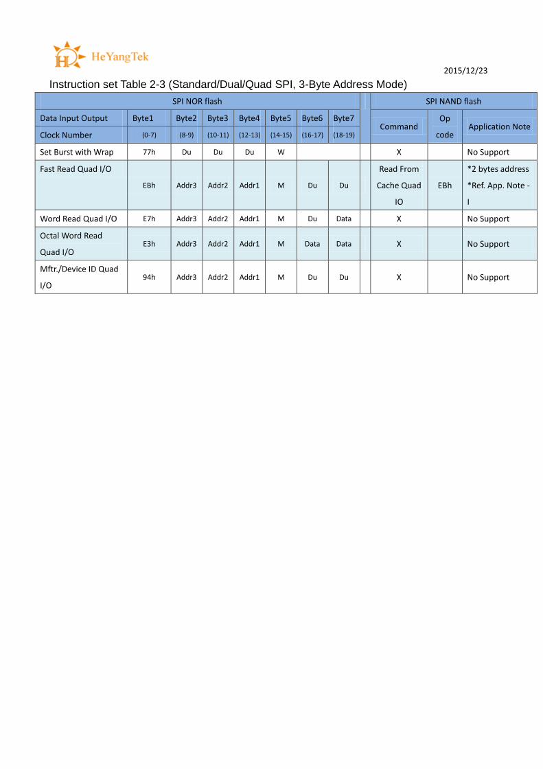
Instruction set Table 2-3 (Standard/Dual/Quad SPI, 3-Byte Address Mode)
SPI NOR flash SPI NAND flash
Data Input Output Byte1 Byte2 Byte3 Byte4 Byte5 Byte6 Byte7 Command
Op
code Application Note
Clock Number (0-7) (8-9) (10-11) (12-13) (14-15) (16-17) (18-19)
Set Burst with Wrap 77h Du Du Du W X No Support
Fast Read Quad I/O
EBh Addr3 Addr2 Addr1 M Du Du
Read From
Cache Quad
IO
EBh
*2 bytes address
*Ref. App. Note -
I
Word Read Quad I/O E7h Addr3 Addr2 Addr1 M Du Data X No Support
Octal Word Read
Quad I/O E3h Addr3 Addr2 Addr1 M Data Data X No Support
Mftr./Device ID Quad
I/O 94h Addr3 Addr2 Addr1 M Du Du X No Support
2015/12/23
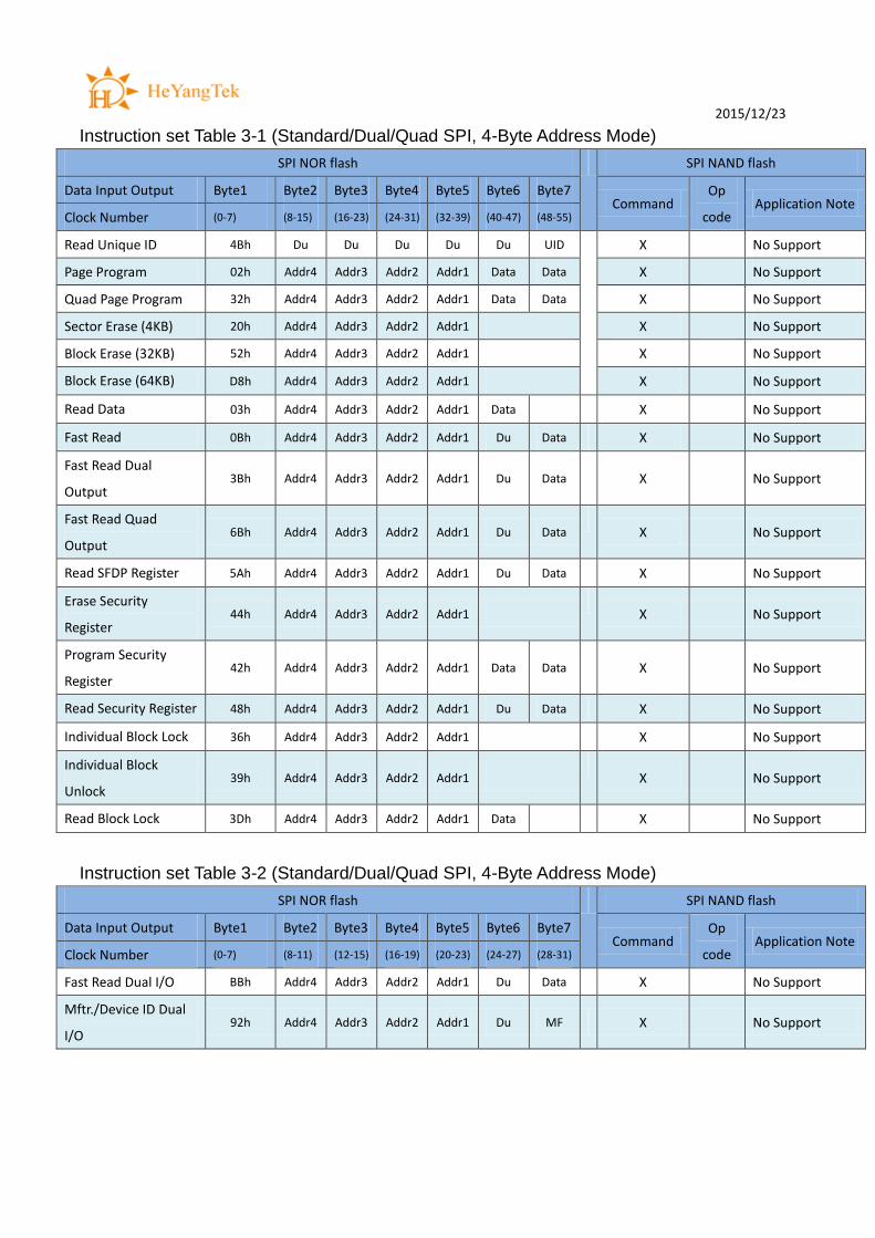
Instruction set Table 3-1 (Standard/Dual/Quad SPI, 4-Byte Address Mode)
SPI NOR flash SPI NAND flash
Data Input Output Byte1 Byte2 Byte3 Byte4 Byte5 Byte6 Byte7 Command
Op
code Application Note
Clock Number (0-7) (8-15) (16-23) (24-31) (32-39) (40-47) (48-55)
Read Unique ID 4Bh Du Du Du Du Du UID X No Support
Page Program 02h Addr4 Addr3 Addr2 Addr1 Data Data X No Support
Quad Page Program 32h Addr4 Addr3 Addr2 Addr1 Data Data X No Support
Sector Erase (4KB) 20h Addr4 Addr3 Addr2 Addr1 X No Support
Block Erase (32KB) 52h Addr4 Addr3 Addr2 Addr1 X No Support
Block Erase (64KB) D8h Addr4 Addr3 Addr2 Addr1 X No Support
Read Data 03h Addr4 Addr3 Addr2 Addr1 Data X No Support
Fast Read 0Bh Addr4 Addr3 Addr2 Addr1 Du Data X No Support
Fast Read Dual
Output 3Bh Addr4 Addr3 Addr2 Addr1 Du Data
X
No Support
Fast Read Quad
Output 6Bh Addr4 Addr3 Addr2 Addr1 Du Data
X No Support
Read SFDP Register 5Ah Addr4 Addr3 Addr2 Addr1 Du Data X No Support
Erase Security
Register 44h Addr4 Addr3 Addr2 Addr1
X No Support
Program Security
Register 42h Addr4 Addr3 Addr2 Addr1 Data Data
X
No Support
Read Security Register 48h Addr4 Addr3 Addr2 Addr1 Du Data X No Support
Individual Block Lock 36h Addr4 Addr3 Addr2 Addr1 X No Support
Individual Block
Unlock 39h Addr4 Addr3 Addr2 Addr1
X No Support
Read Block Lock 3Dh Addr4 Addr3 Addr2 Addr1 Data X No Support
Instruction set Table 3-2 (Standard/Dual/Quad SPI, 4-Byte Address Mode)
SPI NOR flash SPI NAND flash
Data Input Output Byte1 Byte2 Byte3 Byte4 Byte5 Byte6 Byte7 Command
Op
code Application Note
Clock Number (0-7) (8-11) (12-15) (16-19) (20-23) (24-27) (28-31)
Fast Read Dual I/O BBh Addr4 Addr3 Addr2 Addr1 Du Data X No Support
Mftr./Device ID Dual
I/O 92h Addr4 Addr3 Addr2 Addr1 Du MF X No Support

2015/12/23
Instruction set Table 3-3 (Standard/Dual/Quad SPI, 4-Byte Address Mode)
SPI NOR flash SPI NAND flash
Data Input Output Byte1 Byte2 Byte3 Byte4 Byte5 Byte6 Byte7 Command
Op
code Application Note
Clock Number (0-7) (8-9) (10-11) (12-13) (14-15) (16-17) (18-19)
Set Burst with Wrap 77h Du Du Du Du W X No Support
Fast Read Quad I/O EBh Addr4 Addr3 Addr2 Addr1 M Du X No Support
Word Read Quad I/O E7h Addr4 Addr3 Addr2 Addr1 M Du X No Support
Octal Word Read
Quad I/O E3h Addr4 Addr3 Addr2 Addr1 M Data X No Support
Mftr./Device ID Quad
I/O 94h Addr4 Addr3 Addr2 Addr1 M Du X
No Support
Instruction set Table 4 (QPI Instruction, 3-Byte & 4-Byte Address Mode)
SPI NOR flash SPI NAND flash
Data Input Output Byte1 Byte2 Byte3 Byte4 Byte5 Byte6 Command
Op
code Application Note
Clock Number (0,1) (2,3) (4,5) (6,7) (8,9) (10,11)
Write Enable 06h X No Support
Volatile SR Write
Enable 50h X
No Support
Write Disable 04h X No Support
Read Status Register1 05h S7-0 X No Support
Write Status Register1 01h S7-0 X No Support
Read Status Register2 35h S15-8 X No Support
Write Status Register2 31h S15-8 X No Support
Read Status Register3 15h S23-16 X No Support
Write Status Register3 11h S23-16 X No Support
Read Extended Addr.
Register C8h EA
X No Support
Write Extended Addr.
Register C5h EA
X No Support
Chip Erase C7h/60
h
X No Support
Erase/Program
Suspend 75h
X No Support
Erase/Program
Resume 7Ah
X No Support
Power-down B9h X No Support
2015/12/23
Release Power-down
/ ID C0h P
X
No Support
Manufacturer/Device
ID ABh Du Du Du ID
X No Support
JEDEC ID 90h Du Du 00h MF ID X No Support
Global Block Lock 9Fh MF ID15 ID7 X No Support
Global Block Unlock 98h X No Support
Exit QPI Mode FFh X No Support
Enter 4-Bytes Address
Mode B7h
X No Support
Exit 4-Byte Address
Mode E9h
X No Support
Enable Reset 66h X No Support
Reset Device 99h X No Support
Instruction set Table 5 (QPI Instructions, 3-Byte Address Mode)
SPI NOR Flash SPI NAND Flash
Data Input Output Byte1 Byte2 Byte3 Byte4 Byte5 Byte6 Command
Op
code Application Note
Clock Number (0,1) (2,3) (4,5) (6,7) (8,9) (10,11)
Page Program 02h Addr3 Addr2 Addr1 Data Data X No Support
Sector Erase (4KB) 20h Addr3 Addr2 Addr1 X No Support
Block Erase (32KB) 52h Addr3 Addr2 Addr1 X No Support
Block Erase (64KB) D8h Addr3 Addr2 Addr1 X No Support
Fast Read 0Bh Addr3 Addr2 Addr1 Du Data X No Support
Burst Read with Wrap 0Ch Addr3 Addr2 Addr1 Du Data X No Support
Fast Read Quad I/O EBh Addr3 Addr2 Addr1 M Data X No Support
Individual Block Lock 36h Addr3 Addr2 Addr1 X No Support
Individual Block
Unlock 39h Addr3 Addr2 Addr1
X No Support
Read Block Lock 3Dh Addr3 Addr2 Addr1 L Data X No Support
Instruction set Table 6 (QPI Instructions, 4-Byte Address Mode)
SPI NOR flash SPI NAND flash
Data Input Output Byte1 Byte2 Byte3 Byte4 Byte5 Byte6 Byte7 Command
Op
code Application Note
Clock Number (0,1) (2,3) (4,5) (6,7) (8,9) (10,11) (12,12)
Page Program 02h Addr4 Addr3 Addr2 Addr1 Data Data X No Support
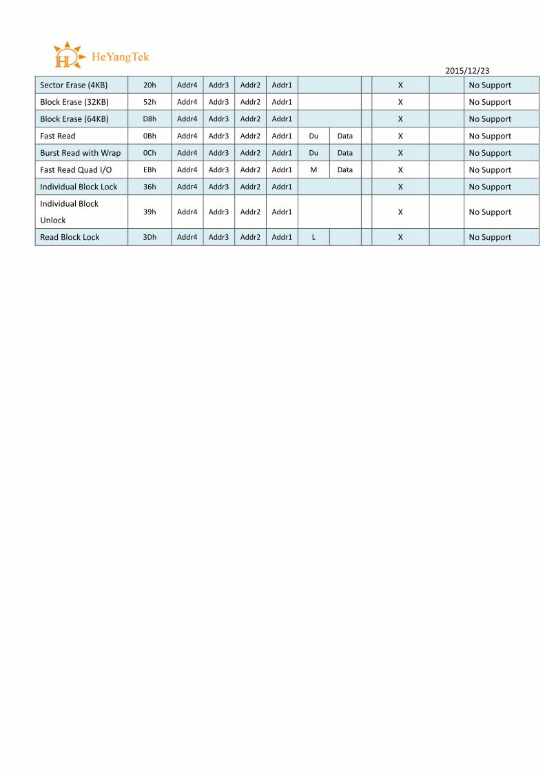
2015/12/23
Sector Erase (4KB) 20h Addr4 Addr3 Addr2 Addr1 X No Support
Block Erase (32KB) 52h Addr4 Addr3 Addr2 Addr1 X No Support
Block Erase (64KB) D8h Addr4 Addr3 Addr2 Addr1 X No Support
Fast Read 0Bh Addr4 Addr3 Addr2 Addr1 Du Data X No Support
Burst Read with Wrap 0Ch Addr4 Addr3 Addr2 Addr1 Du Data X No Support
Fast Read Quad I/O EBh Addr4 Addr3 Addr2 Addr1 M Data X No Support
Individual Block Lock 36h Addr4 Addr3 Addr2 Addr1 X No Support
Individual Block
Unlock 39h Addr4 Addr3 Addr2 Addr1 X No Support
Read Block Lock 3Dh Addr4 Addr3 Addr2 Addr1 L X No Support


![MAINTENANCE MANUAL YAMADA AIR-OPERATED DIAPHRAGM … 032M-12.pdf · DP-5F -----5 DP-5FH ... Loosen four fittings located on the top and bottom of the out chamber assembly. [Fig. 5.6]](https://static.fdocuments.us/doc/165x107/601d6ae94c876e16f256f7c4/maintenance-manual-yamada-air-operated-diaphragm-032m-12pdf-dp-5f-5-dp-5fh.jpg)


![HE 5FH ACB?9M #(!,,%.'%p · 2017. 1. 10. · wñ e hsþih pmri xlexªw jsv ]sy xs nsmr mr hve[mrk fmxw erh eðmrk [svhw erh wsyrh iòigxw l.iv. mechh mrstepclrss . created date: 5/16/2012](https://static.fdocuments.us/doc/165x107/60d705c0438a1b0bea4768ae/he-5fh-acb9m-p-2017-1-10-w-e-hsih-pmri-xlexw-jsv-sy-xs-nsmr.jpg)