PADI IoT Stamp - Pine64files.pine64.org/doc/PADI/documentation/padi-iot-stamp-datasheet.pdf · PADI...
13
PADI IoT Stamp Datasheet PADI IoT Stamp Datasheet Revision 1.0 1
-
Upload
vuongkhanh -
Category
Documents
-
view
217 -
download
3
Transcript of PADI IoT Stamp - Pine64files.pine64.org/doc/PADI/documentation/padi-iot-stamp-datasheet.pdf · PADI...

PADI IoT Stamp Datasheet
PADI IoT Stamp
Datasheet
Revision 1.0
1

PADI IoT Stamp Datasheet
Table of Contents
1. Introduction......................................................................................................................................31.1 Characteristics................................................................................................................................4
1.2 Specifications.................................................................................................................................5
2. Pinout................................................................................................................................................63. Dimension.........................................................................................................................................74. Functional Description.....................................................................................................................84.1 MCU...............................................................................................................................................8
4.2. Memory.........................................................................................................................................8
4.2.1 SRAM and ROM.........................................................................................................................84.2.2 SPI Flash......................................................................................................................................84.3 Maximum Operating Conditions....................................................................................................8
4.4 Recommended Operating Conditions.............................................................................................8
4.5 Digital Port Characteristics.............................................................................................................9
5. RF Parameters..................................................................................................................................96. Power Consumption.......................................................................................................................107. Temperature Drift...........................................................................................................................118. Installation Notes............................................................................................................................12Disclaimer...........................................................................................................................................13
2

PADI IoT Stamp Datasheet
1. Introduction
PADI IoT Stamp, powered by Realtek RTL8710AF, is a highly integrated, single-chip, low power WiFi controller with built-in antenna. The stamp combines an ARM Cortex M3, integrated Flash and RAM, WLAN MAC, WLAN baseband, RF balun, PA, LNA receiver, SAW filter and power management module. Designed for makers with high speed SPI/I2C/UART interfaces for IoTapplications with minimum Printed Circuit Board (PCB) area requirement. The PADI IoT Stamp is even smaller than a US stamp.
Realtek RTL8710AF high performance wireless SOC provides endless possibilities in designing mobile, low power IoT devices at the lowest cost. It can be used as a standalone self-contained WiFi device solution and can also be run as slave module with other MCU as host.
RTL8710AF built-in cache improves system performance and reduces memory requirements. With on board 1MB Flash, PADI IoT stamp can be programmed to run custom firmware that can communicate with external sensors or chipset through various interface ports such as SPI, UART, I2C, PWM and GPIO.
3

PADI IoT Stamp Datasheet
1.1 Characteristics
802.11 b/g/n, CMOS MAC, Baseband PHY
Built-in low power 32-bit CPU as application processor
Built-in TCP/IP protocol stack
Built-in TR Switch, balun, LN, Power Amplifier and Matching Network
Built-in PLL, VLDO and Power Management Components
MO, 2x1 MIMO
A-MPDU, A-MSDU aggregation and 0.4s Guard Interval
WiFi @ 2.4 GHz, Support WPA/WPA2 Security Mode
Support STA/AP/STA+AP Module
Support Smart Config function (include Android and iOS devices)
SPI , UART, I2C, PWM, GPIO
Deep Sleep current 10uA, Shutdown current below 5uA
Wake up, connect and transfer data packets within 2ms
802.11b mode +17dBm Output Power
Standby power below 1.0mW (DTIM3)
Operating Temperature Range: -20oC ~ 85oC
4

PADI IoT Stamp Datasheet
1.2 Specifications
WirelessWiFi Standard:Frequency Range:
802.11 b/g/n2.4 GHz - 2.5 GHz (2400 MHz - 2483.5 MHz)
Hardware
SoC :CPU :ROM / RAM / FLASH :SPI :UART :PWM :I2C :GPIO :Operating Voltage :Operating Temperature :Dimensions :Wireless Network Mode :
Realtek RTL8710AFARM Cortex M3 (83 MHz)1MB / 512KB / 1MBUp to 1 (41.5 Mbps)Up to 3 (2 x 4 Mbps + 1 x 38400 bps)Up to 4Up to 1 (3.4 Mbps)Up to 19 (including 10 GPIO_INT)3.0 V ~ 3.6 V (recommended 3.3 V)-20 ~ 85 ℃ ℃24 mm x 16 mm x 0.8 mmStation / SoftAP / SoftAP + Station
Software
Bitrate :Hash :Security Standard :Encryption :Firmware Update :OS :Development Tools:Network Protocol :User Configuration :
802.11b: 11 Mbps , 802.11g: 54 Mbps , 802.11n: 150 MbpsMD5 / SHA / HMAC-SHAWPA / WPA2WEP / TKIP / AESUART / OTA / JTAGFreeRTOS, ARM® mbed™ (future planning)IAR, openOCD, J-LinkTCP / UDP / HTTP / FTPAT Commands, Cloud Server, Android / iOS APP
5
PADI IoT Stamp Datasheet
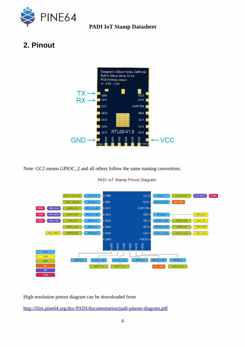
2. Pinout
Note: GC2 means GPIOC_2 and all others follow the same naming convention.
High resolution pinout diagram can be downloaded from
http://files.pine64.org/doc/PADI/documentation/padi-pinout-diagram.pdf
6

PADI IoT Stamp Datasheet
3. Dimension
PADI IoT Stamp dimensions are 24 mm x 16 mm x 3 mm with 3 dBi on-board PCB antenna. The soldering pad size on the bottom layer is 0.9 mm x 1.0 mm.
7

PADI IoT Stamp Datasheet
4. Functional Description
4.1 MCU
Realtek RTL8710AF is a highly integrated, single-chip, low power WiFi 802.11 b/g/n controller with ARM Cortex M3. It also provides some peripheral interface with configurable GPIO.
4.2. Memory
4.2.1 SRAM and ROM
Realtek RTL8710AF has a built-in memory controller for ROM and SRAM. The MCU can access the memory controller by iBus, dBus and AHB interface. These interfaces can access the ROM or SRAM unit as memory arbiters to determine the access sequence. Based on current SDK SRAM usage, the usable SRAM space is more 48 KB.
4.2.2 SPI Flash
PADI IoT Stamp has integrated 1 MB of SPI Flash for custom firmware. External SPI Flash is not supported.
4.3 Maximum Operating Conditions
Operating Conditions Standard Value Units
Storage Temperature -40 to 125 oC
Soldering Temperature 260 oC
Voltage Supply IPC/JEDEC J-STD-020 +3.0 to +3.6 V
4.4 Recommended Operating Conditions
Operating Conditions Label Min Typical Max Units
Operating Temperature -20 20 85 oC
Voltage Supply VDD 3.0 3.3 3.6 V
8

PADI IoT Stamp Datasheet
4.5 Digital Port Characteristics
Port Label Min Typical Max Units
Input Logic Level Low VIL -0.3 0.25VDD V
Input Logic Level High VIH 0.75VDD VDD+0.3 V
Output Logic Level Low VOL N 0.1VDD V
Output Logic Level High VOH 0.8VDD N V
Note: If not specified, the default test condition is VDD = 3.3V, Operating Temperature = 20 oC
5. RF Parameters
Parameters Typical Units
Input Frequency 2412 – 2483.5 MHz
Input Resistance 50 Ω
Output Power 802.11b >17 dBm
802.11g > 15 dBm
802.11n (HT20) > 14 dBm
802.11 (HT40) > 14 dBm
Rx Sensitivity 11M ≤ -76 dBm
54M ≤ -65 dBm
65M (HT20) ≤ -64 dBm
150M (HT40) ≤ -61 dBm
9

PADI IoT Stamp Datasheet
6. Power Consumption
The following power consumption data was measured based on a 3.3 V power supply operating in 25oC using an internal voltage regulator.
All measurements were performed in the absence of the SAW filter, at antenna interface.
All transmitted data is based on a 90% duty cycle, measured in continuous transmission mode.
Mode Min Typical Max Units
Transmitting 802.11b, CCK 11Mbps,POUT= +17dBm
87 mA
Transmitting 802.11g, OFDM 54Mbps, POUT= +15dBm
180 mA
Transmitting 802.11n (HT20), MCS7, POUT= +14dBm
168 mA
Transmitting 802.11n (HT40), MCS7, POUT= +14dBm
148 mA
Receiving 802.11b, packet size 1024 bytes, -76dBm
68 mA
Receiving 802.11g, packet size 1024 bytes, -65dBm
68 mA
Receiving 802.11n, packet size 1024 bytes, -64dBm
68 mA
Modem-Sleep1 15 mA
Light-Sleep2 0.9 mA
Deep-Sleep3 10 µA
Normal Standby 30 mA
Note 1: Modem - Sleep is applied to applications that require CPU in continuous working condition,such as PWM or I2S applications and etc. When WiFi is connected, if there are no data transfer activities, WiFi Modem circuit will be shut down according to 802.11 standards (such as U – APSD) to save power. For example, in DTIM3, which awakens 3ms after every 300 ms sleep time to receive AP Beacon packets and so on, the overall average current consumption is about 15 mA.
Note 2: Light - Sleep is applied to applications where the CPU can be suspended, such as the WiFi switch. When WiFi is connected, if there are no data transfer activities, WiFi Modem circuit will be
10

PADI IoT Stamp Datasheet
shut down according to 802.11 standards (such as U - APSD) and CPU will be suspended to save power. For example, in DTIM3, awake 3ms after every 300 ms sleep time to receive AP Beacon packets and so on, the overall average current consumption is about 0.9 mA.
Note 3: Deep - Sleep is applied to applications that do not require WiFi connection to be active all the time. The application only sends a packet after long time interval, such as in a measurement temperature sensor that only needs to connect every 100 seconds. For example, with the application awake 0.3 s – 1 s to connect AP after every 300 s sleep time, the overall average current consumption can be much lower than 1 mA.
7. Temperature Drift
Temperature Drift TS Max - TL Max 3oC / sec
PreheatTS MinTS TypicalTS MaxT
150oC175oC200oC60 ~ 180 sec
Drift Up (TL to TP) Max 3oC / sec
Temperature (TL) / Time (T) 217oC / 60 ~ 150 sec
Temperature Peak (TP) Max 260oC, duration 10 sec
Target Temperature Peak (Target TP) 260oC +0/-5oC
Actual Peak (tP) 5oC Duration 20 ~ 40 sec
Drift Down Max 6oC / sec
Duration to drift up from 25oC to TP (t) Max 8 minutes
11

PADI IoT Stamp Datasheet
8. Installation Notes
Antenna radiation space is very important. The quality of the environment will affect the transmission distance. Metal or other objects such as motors, cameras, speakers and etc. will directly affect the performance of the antenna, which is equivalent to shielding. PADI IoT Stamp uses on-board PCB antenna which has design requirements depending on the surrounding environment. Don't place any components that will affect antenna performance within 5-10 mm around the antenna and 3 - 5 mm below the antenna. Don’t lay out high frequency signal lines and placing components under the IoT Stamp.
12
PADI IoT Stamp Datasheet
Disclaimer
Pine Microsystems reserves all rights to this document and the information contained herein. Trademarks, logos, names, and designs described herein in whole or in part be subject to intellectualproperty right.
The information, all all content included herein are provided “as is”, with no warranty of any kind, either express or implied, is made in relation to the accuracy, reliability for a particular purpose or content of this document. This document may be revised by Pine Microsystems at any time.
Copyright (c) 2016, Pine Microsystems
13