Pad Crater Project “Idea Project” -...
16
Pad Crater Project “Definition Stage” Joe Smetana Alcatel-Lucent For Member Meeting 2/9/2011 San Jose, CA
Transcript of Pad Crater Project “Idea Project” -...

Pad Crater Project “Definition Stage”
Joe Smetana
Alcatel-Lucent
For Member Meeting 2/9/2011
San Jose, CA

The issue(s)
• Pad Cratering defects are a significant challenge with Pb-free PCB materials and/or Pb-free solders, particularly associated with large BGA devices
• Pad Pull or Ball shear testing has not shown to consistently represent the actual propensity for pad cratering of a material and in some cases can give misleading and/or opposite results from what actually occurs in real assemblies
• A way is needed to rank order materials that is directly related to actual pad cratering

Project Overview
• Create a relatively simple test vehicle with a single large BGA assembled in the middle – 6 or 8 layers, thickness .093
• Fabricate the bare boards from multiple different materials – Include a significant variety of materials, filled and unfilled
– Include materials that have also done “well” in HDPUG Pb-free materials projects
– Don’t test materials that have done poorly in HDPUG Pb-free materials projects
– Other materials as suggested by members
• Perform bend to break testing to rank order the materials – Design TV to virtually ensure trace breaks simultaneous with laminate.
– Spherical bend testing preferred or 4-point bend?
– Other
– Will need to include some amount of strain gage measurements
– Both Single Bend to Break and Repeated Load to Break
• On the same boards ALSO perform HPP testing for a correlation to actual pad cratering. – How valuable is it?
No support for this so far

What this Project will Provide
• Rank order of materials to Pad Cratering in mechanical bend testing
– At selected strain rate • 3000-3500 uε/sec (sweet spot)
– At single bend to break
– At repeated load to break • 60-70%? (TBD) lowest single bend to break load
• Correlation or lack thereof of HPP testing to mechanical bend to break testing
– Currently no support for this

Bend to Break Testing
• Meadville to support Bend to Break
testing
– Need to better define this
– 3000-3500 uε/sec is the sweet spot to
minimize scatter in the results ...
• 1000 and lower introduces a different
failure mode, 6000-7000 exhibits twice the
scatter in the results ... this is typical of
behavior seen in a brittle material.

Simplified Bend to Break Test
This will not
necessarily catch
the first break
point, but should
correlate to it and
should properly
rank order the
materials.

Key Issues
• Define the test component – Practical Components A-PBGA680-1.0mm-35mm-DC-LF-305
• PBGA 680 35x35mm Perimeter+ BGA, 1mm pitch
• 689 x 689 mil die size
• Quote of 1000 for $10,700.00
• Define the materials to be tested – Compare filled vs. unfilled, FR4 – brominated and HF,
Selected High speed materials
– Look at “cap” technologies – such as Zeta
– Select “good” materials (HDPUG Pb-free Materials 1 and 2) • Material suppliers need to supply the materials at no cost
– First Draft/Proposed Material List follows
• Define/Design the Test Board (ALU/Meadville)
• Define the required sample size – 10? Single Bend to Break
– 20? Repeated Bend to Break

Proposed Component
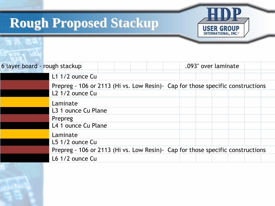
Rough Proposed Stackup
6 layer board - rough stackup
Prepreg - 106 or 2113 (Hi vs. Low Resin)- Cap for those specific constructions
Prepreg - 106 or 2113 (Hi vs. Low Resin)- Cap for those specific constructions
.093" over laminate
Prepreg L4 1 ounce Cu Plane
Laminate L5 1/2 ounce Cu
L6 1/2 ounce Cu
L1 1/2 ounce Cu
L2 1/2 ounce Cu
Laminate L3 1 ounce Cu Plane

Design Rough
Header
for
event
detector
attach
BGA at 45 degrees to allow for either spherical or 4 point bend
Need the following
specifics defined:
• Minimum distance
from component to
board edges?
•What type of
header or board
connector is needed
the event detector?
BGA pattern duplicated on bottom side using either VIP or SMD
pads for comparison

Considerations for Pad Cratering Test
• Materials – Filled vs Unfilled Hi Tg Phenolic Resin
– Halogen Free
– Dicy
– Mid Tg
– High Speed
– Cap Layers
• Resin Content/Glass style effect on outer layers – 106 vs. 2116 between L1-2 and N-N-1
• Pad Size – Normal vs. enlarged solder mask defined pads,
– Enlarged pads at corners
– Microvia in Pad vs. No Microvia in pad (including Dogbone Microvia vs Dogbone Through Via),
– Conformal Microvia vs Filled Micro via Note - With a single design can only do 1 of the options

Preliminary Material List (part 1)
• High Tg Filled Phenolic FR4s – Isola 370HR
– EMC EM-827
– Panasonic R1755V
– Shenzen Pacific (PIC) FL-170
– ITEQ IT-180i
– Panasonic R2125
– Grace GA-170LE
• High Tg Non-filled Phenolic FR4s – Isola 370 Turbo
– Shengyi S1170
– TUC TU-722
• High Tg Halogen Free FR4s – Grace GA-HF-17
– ITEQ IT-170GRA
– EMC EM-370(D) or EMC-370 (one but not both)
– Panasonic R1577 (Megtron 2)
– Shengyi S1165
– Ventec VT-447
– TUC TU-862HF
– Hitachi MCL-HE-679G
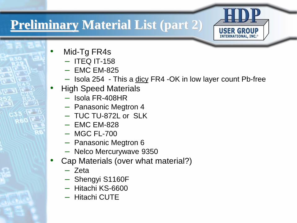
Preliminary Material List (part 2)
• Mid-Tg FR4s – ITEQ IT-158
– EMC EM-825
– Isola 254 - This a dicy FR4 -OK in low layer count Pb-free
• High Speed Materials – Isola FR-408HR
– Panasonic Megtron 4
– TUC TU-872L or SLK
– EMC EM-828
– MGC FL-700
– Panasonic Megtron 6
– Nelco Mercurywave 9350
• Cap Materials (over what material?) – Zeta
– Shengyi S1160F
– Hitachi KS-6600
– Hitachi CUTE

What this Project WILL NOT DO
(as currently planned)
• It will not provide data that necessarily
correlates to pad cratering occurring by
thermo-mechanical stresses – such in
reflow/cooldown as material properties
above Tg will be very different from
those at room temperature.
• If someone has an idea of how to test
this… speak up! It is a critical issue.

Where are we on this Project?
• We have held a few preliminary
meetings and some off-line
discussions with key players
– Everything is currently “draft” and
subject to change
– Delayed “active pursuit” of this project
while we finished the Pb-free materials
project
– Ready for regular meetings to resolve
open issues and move forward

Project Milestones
• Define the full extent of the Project - Team
• Define the test vehicle - Team – Component
– Board (layers, thickness, size, etc.)
• Design the Test Vehicle - ALU
• Determine materials to test - Team
• Determine the required sample sizes - Team
• Material suppliers provide materials at no cost in return for rank ordering (coded)
• Fabricators to build the test vehicle - TBD
• Procure components – Sun +?
• Assemble Test vehicles – Celestica/Flextronics?
• Bend to break testing- Meadville
• Hot Pin Pull testing (assuming we include this)
• Data analysis and reporting