
PACSnumbers: 71.55.-i,71.15.Nc,71.55.Eq71.55.Gs,71.38.-k · nonradiative capture at defects in...
20
arXiv:1407.4197v1 [cond-mat.mtrl-sci] 16 Jul 2014 First-principles theory of nonradiative carrier capture via multiphonon emission Audrius Alkauskas, Qimin Yan, and Chris G. Van de Walle Materials Department, University of California, Santa Barbara, California 93106-5050, USA (Dated: July 17, 2014) We develop a practical first-principles methodology to determine nonradiative carrier capture coefficients at defects in semiconductors. We consider transitions that occur via multiphonon emis- sion. Parameters in the theory, including electron-phonon coupling matrix elements, are computed consistently using state-of-the-art electronic structure techniques based on hybrid density functional theory. These provide a significantly improved description of bulk band structures, as well as defect geometries and wavefunctions. In order to properly describe carrier capture processes at charged centers, we put forward an approach to treat the effect of long-range Coulomb interactions on scattering states in the framework of supercell calculations. We also discuss the choice of initial conditions for a perturbative treatment of carrier capture. As a benchmark, we apply our theory to several hole-capturing centers in GaN and ZnO, materials of high technological importance in which the role of defects is being actively investigated. Calculated hole capture coefficients are in good agreement with experimental data. We discuss the insights gained into the physics of defects in wide-band-gap semiconductors, such as the strength of electron-phonon coupling and the role of different phonon modes. PACS numbers: 71.55.-i, 71.15.Nc, 71.55.Eq 71.55.Gs, 71.38.-k I. INTRODUCTION Point defects drastically affect the performance of semiconductor devices. In particular, they can act as charge traps and/or recombination centers. In electronic applications, such as in high-electron mobility transis- tors, charge traps deteriorate the performance of the de- vice and can lead to so-called device dispersion. 1 In most cases charge trapping, or capture, occurs nonradiatively, i.e., without the emission of a photon. In optoelectronic applications, such as in light-emitting diodes or photo- voltaic cells, defects can act as recombination centers for charge carriers. This so-called Shockley-Read-Hall (SRH) recombination 2 is detrimental, as it decreases the efficiency of the device. SRH recombination can also af- fect electronic devices that rely on minority carrier trans- port, e.g., bipolar transistors. SRH recombination is a sequence of two carrier capture processes: one carrier is captured, and then the other carrier recombines with it. 2 For both charge traps and recombination centers, the important question is: what are the carrier capture coef- ficients (cross sections)? For deep centers the nonradiative carrier capture oc- curs via multiphonon emission (MPE). 2–4 The main idea behind MPE is that the transition between the delocal- ized bulk state and the localized defect state can occur within the first order of electron-phonon coupling because of a large local lattice relaxation associated with the change of the charge state of the defect. 2–4 The phonon selection rule Δn = ±1 is relieved, and emission of more than one phonon becomes possible. Many researchers have contributed to the theoretical foundations of MPE over the past six decades. 4–15 These investigations have revealed that the results of calculations are extremely sensitive to (i) the adopted theoretical model and (ii) the details of the electronic structure of the defect, with different approaches yielding variations of capture coeffi- cients over many orders of magnitude. 16 Concerning aspect (i), earlier theoretical works 4–15 have made it clear that there is no single theoretical model that is valid in all cases. A number of fac- tors have to be considered in choosing the appropri- ate description, 4–15 including the hierarchy of differ- ent time scales (carrier capture times vs. phonon life- times and periods of lattice vibrations), the strength of electron-phonon coupling (linear vs. higher-order cou- pling schemes), the choice of a good starting point for perturbation theory (electron and phonon wavefunc- tions), and the number of different phonon modes that have to be considered. This choice of description has to be considered for each type of defect individually, a practice we will follow in the current paper as well. Aspect (ii), i.e., incomplete knowledge of the atomic and electronic structure of the defect, turned out to be an equally important issue. If this structure is not known, not only does it affect the result within a given theoretical model, but it impedes the choice of the correct model it- self. Aspect (ii) is thus closely linked to aspect (i). When the objective was to understand general trends and inter- pret experimental findings, calculations based on models that did not take the specifics of the atomic and the elec- tronic structure into account were often very successful. An example of such work is the seminal paper of Henry and Lang 4 on nonradiative carrier capture in GaP and GaAs, semiconductors with room-temperature band gaps of 2.22 and 1.42 eV, 17 respectively. The authors theoreti- cally determined the temperature dependence of capture cross sections and provided an estimate of the range of high-temperature asymptotic values of these cross sec- tions. Using a semi-classical description of carrier cap- ture, they could explain the exponential dependence of cross sections on temperature for many defects in both
Transcript of PACSnumbers: 71.55.-i,71.15.Nc,71.55.Eq71.55.Gs,71.38.-k · nonradiative capture at defects in...
arX
iv:1
407.
4197
v1 [
cond
-mat
.mtr
l-sc
i] 1
6 Ju
l 201
4
First-principles theory of nonradiative carrier capture via multiphonon emission
Audrius Alkauskas, Qimin Yan, and Chris G. Van de WalleMaterials Department, University of California, Santa Barbara, California 93106-5050, USA
(Dated: July 17, 2014)
We develop a practical first-principles methodology to determine nonradiative carrier capturecoefficients at defects in semiconductors. We consider transitions that occur via multiphonon emis-sion. Parameters in the theory, including electron-phonon coupling matrix elements, are computedconsistently using state-of-the-art electronic structure techniques based on hybrid density functionaltheory. These provide a significantly improved description of bulk band structures, as well as defectgeometries and wavefunctions. In order to properly describe carrier capture processes at chargedcenters, we put forward an approach to treat the effect of long-range Coulomb interactions onscattering states in the framework of supercell calculations. We also discuss the choice of initialconditions for a perturbative treatment of carrier capture. As a benchmark, we apply our theoryto several hole-capturing centers in GaN and ZnO, materials of high technological importance inwhich the role of defects is being actively investigated. Calculated hole capture coefficients are ingood agreement with experimental data. We discuss the insights gained into the physics of defectsin wide-band-gap semiconductors, such as the strength of electron-phonon coupling and the role ofdifferent phonon modes.
PACS numbers: 71.55.-i, 71.15.Nc, 71.55.Eq 71.55.Gs, 71.38.-k
I. INTRODUCTION
Point defects drastically affect the performance ofsemiconductor devices. In particular, they can act ascharge traps and/or recombination centers. In electronicapplications, such as in high-electron mobility transis-tors, charge traps deteriorate the performance of the de-vice and can lead to so-called device dispersion.1 In mostcases charge trapping, or capture, occurs nonradiatively,i.e., without the emission of a photon. In optoelectronicapplications, such as in light-emitting diodes or photo-voltaic cells, defects can act as recombination centersfor charge carriers. This so-called Shockley-Read-Hall(SRH) recombination2 is detrimental, as it decreases theefficiency of the device. SRH recombination can also af-fect electronic devices that rely on minority carrier trans-port, e.g., bipolar transistors. SRH recombination is asequence of two carrier capture processes: one carrieris captured, and then the other carrier recombines withit.2 For both charge traps and recombination centers, theimportant question is: what are the carrier capture coef-ficients (cross sections)?
For deep centers the nonradiative carrier capture oc-curs via multiphonon emission (MPE).2–4 The main ideabehind MPE is that the transition between the delocal-ized bulk state and the localized defect state can occurwithin the first order of electron-phonon coupling becauseof a large local lattice relaxation associated with thechange of the charge state of the defect.2–4 The phononselection rule ∆n = ±1 is relieved, and emission of morethan one phonon becomes possible. Many researchershave contributed to the theoretical foundations of MPEover the past six decades.4–15 These investigations haverevealed that the results of calculations are extremelysensitive to (i) the adopted theoretical model and (ii)the details of the electronic structure of the defect, with
different approaches yielding variations of capture coeffi-cients over many orders of magnitude.16
Concerning aspect (i), earlier theoretical works4–15
have made it clear that there is no single theoreticalmodel that is valid in all cases. A number of fac-tors have to be considered in choosing the appropri-ate description,4–15 including the hierarchy of differ-ent time scales (carrier capture times vs. phonon life-times and periods of lattice vibrations), the strength ofelectron-phonon coupling (linear vs. higher-order cou-pling schemes), the choice of a good starting pointfor perturbation theory (electron and phonon wavefunc-tions), and the number of different phonon modes thathave to be considered. This choice of description hasto be considered for each type of defect individually, apractice we will follow in the current paper as well.
Aspect (ii), i.e., incomplete knowledge of the atomicand electronic structure of the defect, turned out to bean equally important issue. If this structure is not known,not only does it affect the result within a given theoreticalmodel, but it impedes the choice of the correct model it-self. Aspect (ii) is thus closely linked to aspect (i). Whenthe objective was to understand general trends and inter-pret experimental findings, calculations based on modelsthat did not take the specifics of the atomic and the elec-tronic structure into account were often very successful.An example of such work is the seminal paper of Henryand Lang4 on nonradiative carrier capture in GaP andGaAs, semiconductors with room-temperature band gapsof 2.22 and 1.42 eV,17 respectively. The authors theoreti-cally determined the temperature dependence of capturecross sections and provided an estimate of the range ofhigh-temperature asymptotic values of these cross sec-tions. Using a semi-classical description of carrier cap-ture, they could explain the exponential dependence ofcross sections on temperature for many defects in both
2
GaAs and GaP, which proved that for these systems car-rier capture was indeed due to multiphonon emission.However, their model was unable to offer specific predic-tions for individual defects, and provided little insightinto exceptions to the general trends. In addition, theseas well as other early calculations required empirical in-put as well as drastic simplifications regarding the lo-cal electronic structure and the nature of relevant latticevibrations. This seriously limited the predictive power,especially for applications to new materials.
With the advent of accurate electronic structure meth-ods, mostly based on density functional theory (DFT)and related techniques, the situation is very differentnow.18,19 State-of-the-art approaches, such as hybridfunctionals, provide a very good description of both bulkband gaps and localized defect states.20 The availabilityof these methods, combined with the general knowledgeof MPE acquired over the past six decades, raises thequestion whether nonradiative carrier capture rates cannow be determined completely from first principles, al-lowing them to be used predictively, and whether suchcalculations can expand our insights into the physics ofdefects. This provides the motivation for our work.
Some progress has already been made in thisarea. Schanovsky and co-workers studied nonra-diative hole trapping at defects in SiO2 and ad-dressed the vibrational part of the problem usingfirst-principles calculations,21,22 but actual values ofthe electron-phonon matrix elements remained undeter-mined. McKenna and Blumberger23 studied the re-lated problem of electron transfer between defect stateswithin the Marcus theory,24 and determined the electron-phonon coupling matrix element between two localizeddefect states in MgO directly from electronic structurecalculations. Shi and Wang25 were the first to addressboth the vibrational and the electron-phonon part of thecarrier-capture problem completely from electronic struc-ture calculations. They presented an algorithm to cal-culate electron-phonon matrix elements at defects, andapplied the methodology to study hole capture at theZnGa-VN complex in GaN. Despite some important con-tributions, this study also had some limitations. First,the theory was applied to a defect for which direct experi-mental data is not available.26 Second, both ground-stategeometries of the defect and electron-phonon matrix el-ements were determined using a semilocal functionalwithin the so-called generalized gradient approximation(GGA). Such functionals underestimate bulk band gapsand tend to over-delocalize defect wavefunctions. As dis-cussed in Sec. III, more accurate approaches are availablethat overcome these drawbacks. Third, as we analyze inSec. V, the theoretical approach used in Ref. 25, the so-called adiabatic formulation within the Condon approx-imation, can be questioned for describing nonradiativecapture at defects.10,12
Overall, it is clear that the current status of modelingnonradiative capture at defects in solids is still unsatis-factory, especially when contrasted with the impressive
advances in treating electron-phonon coupling in defect-free crystals,27,28 or in describing nonradiative processesin molecules.29
In this work we present calculations of carrier cap-ture rates via MPE entirely from first principles. Theelectronic structure, the vibrational properties, and theelectron-phonon coupling are determined from accurateelectronic structure techniques, in particular hybrid den-sity functional theory. Specifically, we present a methodto calculate electron-phonon coupling matrix elementsat defects consistently within the hybrid functional ap-proach. Our calculations yield absolute carrier cap-ture rates without any fitting parameters. We applythe methodology to a set of defects in GaN and ZnO,wide-band-gap semiconductors with T=0 K band gapsof 3.5030 and 3.44 eV,31 respectively. We first study CN
in GaN and LiZn in ZnO because optical signatures ofthese two defects are well established32–38 and nonradia-tive capture coefficients are available.35 We also apply ourmethodology to the ZnGa-VN defect in GaN to compareour results with those of Ref. 25.This paper is organized as follows. The problem of
nonradiative carrier capture is described in Section II. InSection III we outline the theoretical formulation of theMPE, present technical details of our computational tool-box, and discuss how various quantities are calculated.In Section IV we present results for selected defects inGaN and ZnO and compare with available experimentaldata and other computational approaches. In Section Vwe critically analyze our approach and discuss insightsgained into defect physics in GaN and ZnO. Section VIconcludes the paper.
II. DEFINITION OF THE PROBLEM
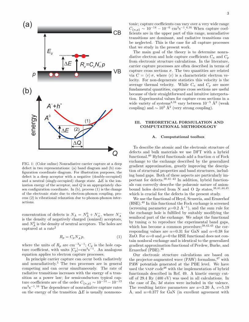
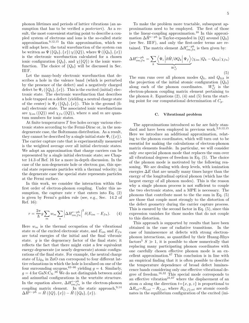
Without loss of generality, let us consider nonradia-tive carrier capture of a hole by an acceptor defect.The process is illustrated in Fig. 1 in two different rep-resentations: (a) a band diagram, and (b) a configu-ration coordinate (cc) diagram. In the latter, a one-dimensional generalized coordinateQ is used to representatomic relaxations.16 The excited state of the system cor-responds to the negatively charged acceptor and a holein the valence band (A−+h+), while the ground statecorresponds to the neutral state of the acceptor (A0).The equilibrium geometries of the two charge states aredifferent. ∆E is the energy difference between the twostates.Carrier capture consists of two elementary steps:
an energy-conserving transition between two electronicstates, process (1), and vibrational relaxation, process(2), in Fig. 1(b). Vibrational relaxation occurs on atimescale of a few picoseconds,39 while the electronictransition is much slower.4 Thus, the electronic transi-tion is the bottleneck for nonradiative capture, and inthis work we will only consider process (1).Let p be the density of holes in the system. The total
3
VB
CB
R = N pp p AC_
DE
Q
A h_
++
energ
y
(a)
(b)
DE
A0
DQ
Eg
(1)
(2)
p
FIG. 1: (Color online) Nonradiative carrier capture at a deepdefect in two representations: (a) band diagram and (b) con-figuration coordinate diagram. For illustration purposes, thedefect is a deep acceptor with a negative (doubly-occupied)and a neutral (singly-occupied) charge state. ∆E is the ion-ization energy of the acceptor, and Q is an appropriately cho-sen configuration coordinate. In (b), process (1) is the changeof the electronic state due to electron-phonon coupling, pro-cess (2) is vibrational relaxation due to phonon-phonon inter-actions.
concentration of defects is NA = N0A + N−
A , where N−A
is the density of negatively charged (ionized) acceptors,and N0
A is the density of neutral acceptors. The holes arecaptured at a rate2
Rp = CpN−A p, (1)
where the units of Rp are cm−3s−1; Cp is the hole cap-ture coefficient, with units [Cp]=cm3s−1. An analogousequation applies to electron capture processes.In principle carrier capture can occur both radiatively
and nonradiatively.5 The two processes are in generalcompeting and can occur simultaneously. The rate ofradiative transitions increases with the energy of a tran-sition as a power law; for semiconductors typical cap-ture coefficients are of the order Cn,p ∼ 10−14 − 10−13
cm3s−1.16 The dependence of nonradiative capture rateson the energy of the transition ∆E is usually nonmono-
tonic; capture coefficients can vary over a very wide rangeCn,p ∼ 10−14 − 10−6 cm3s−1.4,16 When capture coef-ficients are in the upper part of this range, nonradiativetransitions are dominant, and radiative transitions canbe neglected. This is the case for all capture processesthat we study in the present work.The main goal of the theory is to determine nonra-
diative electron and hole capture coefficients Cn and Cp
from electronic structure calculations. In the literature,carrier capture processes are often described in terms ofcapture cross sections σ. The two quantities are relatedvia C = 〈v〉 σ, where 〈v〉 is a characteristic electron ve-locity. For non-degenerate statistics this velocity is theaverage thermal velocity. While Cn and Cp are morefundamental quantities, capture cross sections are usefulbecause of their straightforward and intuitive interpreta-tion. Experimental values for capture cross sections in awide variety of systems4,16 vary between 10−5 A2 (weakcoupling) and ∼ 103 A2 (very strong coupling).
III. THEORETICAL FORMULATION AND
COMPUTATIONAL METHODOLOGY
A. Computational toolbox
To describe the atomic and the electronic structure ofdefects and bulk materials we use DFT with a hybridfunctional.40 Hybrid functionals add a fraction α of Fockexchange to the exchange described by the generalizedgradient approximation, greatly improving the descrip-tion of structural properties and band structures, includ-ing band gaps. Both of these aspects are particularly im-portant for defects.38,41–43 In addition, hybrid function-als can correctly describe the polaronic nature of anion-bound holes derived from N and O 2p states,38,41,44,45
which is crucial for the defects in the present study.We use the functional of Heyd, Scuseria, and Ernzerhof
(HSE).40 In this functional the Fock exchange is screened(screening parameter µ=0.2 A−1), and the sum rule forthe exchange hole is fulfilled by suitably modifying thesemilocal part of the exchange. We adapt the functionalby tuning α to reproduce the experimental band gaps,which has become a common procedure;38,42,43 the cor-responding values are α=0.31 for GaN and α=0.38 forZnO. For α=0 and µ=0 the HSE functional does not con-tain nonlocal exchange and is identical to the generalizedgradient approximation functional of Perdew, Burke, andErnzerhof (PBE).46
Our electronic structure calculations are based onthe projector-augmented wave (PAW) formalism,47 withPAW potentials generated at the PBE level. We haveused the vasp code48 with the implementation of hybridfunctionals described in Ref. 49. A kinetic energy cut-off of 29.4 Ry (400 eV) was used in all calculations. Inthe case of Zn, 3d states were included in the valence.The resulting lattice parameters are a=3.20 A, c=5.19A, and u=0.377 for GaN (in excellent agreement with
4
the experimental50 values 3.19 A, 5.20 A, and 0.377, re-spectively); and a=3.24 A, c=5.21 A, and u=0.379 forZnO (experimental50 values 3.25 A, 5.20 A, and 0.382).Defects were modeled using the supercell
methodology.18 The defect calculations used 96-atom wurtzite supercells, with the lattice parametersoptimized at the HSE level. In the calculation offormation energies of charged defects, as well as charge-state transition levels (ionization potentials), finite-sizecorrections as proposed in Ref. 51 were included. TheBrillouin zone was sampled at one special k-point.52
For test systems, these calculations produce results fordefect levels within 0.03 eV of those obtained with a2×2×2 mesh.While most of our calculations were performed using
the PAW methodology, it makes calculations of electron-phonon coupling matrix elements quite cumbersome.Such calculations are greatly facilitated within the plane-wave pseudopotential (PW-PP) formalism,53 which weadopted for this purpose. Norm-conserving Troullier-Martins pseudopotentials (PPs)54 were generated at thePBE level using the fhi98pp program.55 3d states wereincluded in the valence for both Zn and Ga. The energycutoff for plane-wave expansion of wavefunctions was setto 80 Ry in GaN and 100 Ry in ZnO. We used the cpmdcode,56 with the implementation of hybrid functionalsdiscussed in Refs. 57, 58, and 59. Brillouin-zone sam-pling in these calculations was performed using a singleΓ point. In order to reproduce experimental band gaps,α values of 0.38 for GaN and 0.47 for ZnO had to beused in these PP calculations, i.e., larger than in thePAW calculations. We attribute this to the generationof PPs at the PBE level, rather than consistently withhybrid functionals (cf. Refs. 43,58–61). However, for pa-rameters for which direct comparisons can be made, suchas total energy differences, equilibrium atomic configura-tions, or vibrational frequencies, the PW-PP calculationsare in gratifyingly good agreement with the PAW results;for instance, charge-state transition levels for the defectsconsidered here differ by 0.09 eV or less.
B. Derivation of the capture coefficient
Let us consider a hole capture process at a single ac-ceptor, as in Fig. 1; the discussion can be easily adaptedto other cases. Let V be a large volume that contains Pholes, their density being p = P/V , and M−
A the totalnumber of hole-capturing defects in the appropriate neg-ative charge state, with a density of N−
A=M−A /V . The
total density of defects is NA = N0A + N−
A . Under non-equilibrium steady-state conditions, both electrons andholes can be present in the system. Mobile carriers screenthe Coulomb potential of impurities, with a screeninglength λ. (For neutral impurities, λ would be the ex-tent of their short-range potential.) A few distances λaway from each impurity the potential essentially van-ishes. We will assume that λ3NA ≪ 1, implying that the
region where the potential is not negligible constitutes avery small part of the solid. Since the hole density nearthe impurity is obviously different from p, this assump-tion means that the hole density in the space where thepotential of impurity atoms can be neglected is equal tothe average density, i.e., p. A similar condition λ3p ≪ 1(i.e., λ ≪ p−1/3) allows us to assume that two holes donot interact with the same impurity at the same time.Computationally the most convenient quantity to cal-
culate is the capture rate of one hole at one defect in thewhole volume V . Let the capture rate for such processbe r ([r]=s−1). The capture rate of P holes at all iden-tical M−
A defects (all in their negative charge states) in
volume V is then γp=rM−AP ([γ]=s−1). We can rewrite
this equation as (γp/V ) = rV × (M−A /V ) × (P/V ) =
(rV )N−A p. By comparing this equation with Eq. (1), and
noting that, by definition γp/V = Rp is the capture rateper unit volume, we see that the hole capture coefficientis given by:
Cp = V r. (2)
From now on consider only one hole being captured byone defect.The general idea behind nonradiative processes due to
multiphonon emission is closely related to the conceptof electron-phonon coupling in bulk solids.62 We brieflyreview the main ideas, emphasizing the aspects specificto defects. The many-body Hamiltonian of the entiresystem of electrons and ions is
H = TI + Te + VII + Vee + VIe, (3)
where T represents kinetic energy, V represents Coulombinteraction, and the subscript “e” is for electrons and“I ” for ions. For an isolated system at zero temperaturethe solution of the Schrodinger equation HΨn = EnΨn
yields the energy spectrum En and many-body wave-functions Φn (Q, x). x represents all electronicdegrees of freedom and Q represent all ionic coordi-nates (which can be transformed to phonon coordinatesin the harmonic approximation). In most practical situ-ations, however, it is more useful to describe the systemnot via eigenstates of the full Hamiltonian H , but viaeigenstates of a simpler Hamiltonian H0 that encodesthe essential physics of the system.62 Eigenstates of H0
can be written as a product of the electronic and theionic part. The term ∆H = H − H0 is then the per-turbation that causes transitions between eigenstates ofH0. These transitions should be rare in order to ensurethat the Hamiltonian H0 captures the essential physicsof the system.62 The part of ∆H that is due to the ionsand that induces transitions between different electronicstates, such as in the case of nonradiative carrier capture,is the electron-phonon coupling ∆He−ph. The remainingpiece describes electron-electron and phonon-phonon in-teractions that are not discussed further.The time scale associated with carrier capture pro-
cesses in semiconductors is usually much larger than both
5
phonon lifetimes and periods of lattice vibrations (an as-sumption that has to be verified a posteriori). As a re-sult, the most convenient starting point to describe a cou-pled system of electrons and ions is the so-called staticapproximation.9,12,15 In this approximation, which wewill adopt here, the total wavefunction of the system canbe written as Ψ (Q0, x)χ(Q), where Ψ (Q0, x)is the electronic wavefunction calculated for a chosenionic configuration Q0, and χ(Q) is the ionic wave-function. The choice of Q0 will be discussed in Sec.III F.Let the many-body electronic wavefunction that de-
scribes a hole in the valence band (which is perturbedby the presence of the defect) and a negatively chargeddefect be Ψi (Q0, x). This is the excited (initial) elec-tronic state. The electronic wavefunction that describesa hole trapped on a defect (yielding a neutral charge stateof the center) is Ψf (Q0, x). This is the ground (fi-nal) electronic state. The associated ionic wavefunctionsare χim (Q) and χfn (Q), where n and m are quan-tum numbers for ionic states.At finite temperatures T free holes occupy various elec-
tronic states according to the Fermi-Dirac or, in the non-degenerate case, the Boltzmann distribution. As a result,they cannot be described by a single initial state Ψi (x).The carrier capture rate that is experimentally measuredis the weighted average over all initial electronic states.We adopt an approximation that charge carriers can berepresented by a single initial electronic state; see Chap-ter 14.3 of Ref. 16 for a more in-depth discussion. In thecase of the non-degenerate hole or electron gas, this spe-cial state represents particles with a thermal velocity; inthe degenerate case the special state represents particlesat the Fermi surface.In this work, we consider the interaction within the
first order of electron-phonon coupling. Under this as-sumption, the capture rate r that enters into Eq. (2)is given by Fermi’s golden rule (see, e.g., Sec. 14.2 ofRef. 16):
r =2π
~g∑
m
wm
∑
n
∣∣∣∆H
e−phim;fn
∣∣∣
2
δ(Eim − Efn). (4)
Here wm is the thermal occupation of the vibrationalstate m of the excited electronic state, and Eim and Efn
are total energies of the initial and the final vibronicstate. g is the degeneracy factor of the final state; itreflects the fact that there might exist a few equivalentenergy-degenerate (or nearly degenerate) atomic configu-rations of the final state. For example, the neutral chargestate of LiZn in ZnO can correspond to four different lat-tice relaxations in which the hole is localized on one of thefour surrounding oxygens,63–66 yielding g = 4. Similarly,g = 4 for GaN:CN.
38 We do not distinguish between axialand azimuthal configurations in the wurtzite structure.
In the equation above, ∆He−phim;fn is the electron-phonon
coupling matrix element. In the static approach,9,14
∆He−ph = H (Q, x)− H (Q0, x).
To make the problem more tractable, subsequent ap-proximations need to be employed. The first of thoseis the linear-coupling approximation.16 In this approxi-mation ∆He−ph is Taylor-expanded in Q around Q0(see Sec. III F), and only the first-order terms are re-
tained. The matrix element ∆He−phim;fn is then given by:
∆He−phim;fn =
∑
k
⟨
Ψi
∣∣∣∂H/∂Qk
∣∣∣Ψf
⟩
︸ ︷︷ ︸
Wkif
〈χim |Qk −Q0;k|χfn〉
(5)The sum runs over all phonon modes Qk, and Q0;k isthe projection of the initial atomic configuration Q0along each of the phonon coordinates. W k
if is theelectron-phonon coupling matrix element pertaining tothe phonon k. Equations (2), (4) and (5) form the start-ing point for our computational determination of Cp.
C. Vibrational problem
The approximations introduced so far are fairly stan-dard and have been employed in previous work.2,9,12,15
Here we introduce an additional approximation, relat-ing to the phonon coordinates, which will turn out to beessential for making the calculations of electron-phononmatrix elements feasible. In particular, we will consideronly one special phonon mode that replaces the sum overall vibrational degrees of freedom in Eq. (5). The choiceof the phonon mode is motivated by the following rea-soning. We are dealing with deep levels, with ionizationenergies ∆E that are usually many times larger than theenergy of the longitudinal optical phonon (which has thelargest energy of all phonon modes). This is the reasonwhy a single phonon process is not sufficient to couplethe two electronic states, and a MPE is necessary. Thephonons that contribute most to the the sum in Eq. (5)are those that couple most strongly to the distortion ofthe defect geometry during the carrier capture process.This is ensured by the second factor in Eq. (5), since thisexpression vanishes for those modes that do not coupleto this distortion.This approach is supported by results that have been
obtained in the case of radiative transitions. In thecase of luminescence at defects with strong electron-phonon interactions, as quantified by their Huang-Rhysfactors5 S ≫ 1, it is possible to show numerically thatreplacing many participating phonon coordinates withone carefully chosen effective phonon mode is an ex-cellent approximation.67 This conclusion is in line withan empirical finding that it is often possible to describethe temperature dependence of broad defect lumines-cence bands considering only one effective vibrational de-gree of freedom.16,32 This special mode corresponds toan effective vibration21,67 where the displacement of anatom α along the direction t=x, y, z is proportional to∆Rαt=Ri;αt − Rf ;αt, where Ri,f;αt are atomic coordi-nates in the equilibrium configuration of the excited (ini-
6
tial) and the ground (final) state. In this one-dimensionalmodel the generalized configuration coordinate Q for val-ues of atomic positions Rαt that correspond to this dis-placement is
Q2 =∑
α,t
mα (Rαt −Rf ;αt)2, (6)
where mα are atomic masses. The geometry of theground state (final state f) corresponds to Q=0, whilethe geometry of the excited state (initial state i) corre-sponds to Q=∆Q with
(∆Q)2 =∑
α,t
mα∆R2αt, (7)
In this description the configuration coordinate of Eq.(6) has units of amu1/2A (amu - atomic mass unit). Wewill give a brief description of changes of the defect ge-ometry encoded in ∆Q when discussing specific systemsin Section IV. The plot that shows the total energiesin the ground and the excited states Ei,f as a func-tion of Q is called the configuration coordinate diagram(cc diagram)16; we have shown a schematic example inFig. 1(b). The frequency of the effective vibration in theground and the excited state is given as
Ω2i,f =
∂2Ei,f
∂Q2. (8)
An auxiliary quantity (∆R)2=∑
α,t ∆R2αt, allows to de-
fine the modal mass of the vibration via ∆Q=M1/2∆R.21
The knowledge of M is useful for interpreting the valueof Ω for different defects.67 A very useful dimensionlessquantity is the Huang-Rhys factor, defined as5,67
Si,f =1
2~(∆Q)2Ωi,f. (9)
The case S ≫ 1 corresponds to large lattice relaxationsassociated with the change of the charge state. We notethat the special mode Q is not an eigenstate of the vi-brational Hamiltonian, but it serves as a very useful ap-proximation and has a clear physical meaning. Possibleerrors introduced by the use of the one-dimensional ap-proximation are critically reviewed in Sec. VB.
D. Electron-phonon matrix elements
Thanks to the one-dimensional (1D) approximation de-scribed in Sec. III C we have to determine only a singleelectron-phonon coupling matrix element:
Wif =⟨
Ψi
∣∣∣ ∂H/∂Q
∣∣∣Ψf
⟩
. (10)
At this stage, Ψi,f are still many-electron wavefunc-
tions, and H is the many-body Hamiltonian of the sys-tem. In an independent-particle picture corresponding
to the (generalized) Kohn-Sham approach of DFT, wewill assume that the many-body Hamiltonian and many-electron wavefunctions in Eq. (10) can be replaced by
their single-particle counterparts h and ψi,f, i.e.:
Wif =⟨
ψi
∣∣∣ ∂h/∂Q
∣∣∣ψf
⟩
. (11)
Whereas wavefunctions Ψi,f describe the entire elec-tronic system, single-particle wavefunctions ψi,f havea different meaning: ψi corresponds to the hole in thevalence band perturbed by the presence of the defect,and ψf is the localized defect state. Indeed, for pertur-bation theory to be physically meaningful, both statesψi,f have to be eigenstates of the same Hamiltonian:the initial state has to correspond to the perturbed holestate rather than a hole state in an unperturbed bulkmaterial.To calculate electron-phonon matrix elements we use
hybrid functionals within the PW-PP approach, as dis-
cussed in Sec. III A. Therefore, h contains nonlocal Fockexchange, as well as the nonlocal part of pseudopoten-tials. These terms would have to be calculated explicitlyif Eq. (11) were used. To avoid such a cumbersome pro-cedure, it is extremely convenient to use an alternativeexpression that follows directly from perturbation theory[e.g., Eq. (28) in Ref. 27]:
Wif =
⟨
ψi
∣∣∣∣∣
∂h
∂Q
∣∣∣∣∣ψf
⟩
= (εi − εf)
⟨
ψi
∣∣∣∣
∂ψf
∂Q
⟩
(12)
In this expression the main effort in calculating the ma-trix element boils down to the calculation of the deriva-tive ∂ψf/∂Q. This is accomplished by evaluating thederivative numerically via finite differences, as discussedfor specific defects in Sec. III F.
E. Bulk scattering states
The methodology outlined in Sec. III B above relieson calculating the capture rate r for one hole, with a fi-nite velocity, at one defect in the entire (large) volumeV . The role of all other carriers is to screen the long-range Coulomb interaction between the hole and the de-fect. The electron-phonon coupling matrix element forone special phonon mode is determined via Eq. (12), andthe capture coefficient Cp is subsequently determined viaEqs. (2), (4) and (5). Only one phonon coordinate isretained in expression (5).The problem with this formulation is the following.
Actual calculations are performed for a system with arelatively small volume, the supercell with a volume Vthat is constrained by computational limitations. Whilethere is plenty of evidence that the localized defect stateψf is accurately represented in such supercell calcula-tions, this is not necessarily the case for the initial per-turbed bulk state ψi. In particular, if the capturing cen-ter is charged, the screened Coulomb interaction between
7
the defect and the carrier significantly affects the captureprocesses. Such interactions are not well represented inthe supercell calculation. Let us picture, as an example,a charged carrier with a vanishing kinetic energy beingcaptured at a repulsive center. As the size of the sys-tem V grows, the particle is expelled further and furtheraway from the defect. In the limit of an infinite volumeV , and zero kinetic energy of the charge carrier, the cap-ture rate would tend to zero. However, in the supercellof volume V the carrier cannot be expelled to infinity,and the capture rate remains finite, which is an incorrectphysical result. Similar considerations also apply to at-tractive centers and emphasize the need of the correctionterm, which we discuss here.Let the electron-phonon coupling matrix element cal-
culated in the computational supercell be Wif . It is cal-culated via the equation, similar to Eq. (12):
Wif =
⟨
ψi
∣∣∣∣∣
∂h
∂Q
∣∣∣∣∣ψf
⟩
= (εi − εf )
⟨
ψi
∣∣∣∣
∂ψf
∂Q
⟩
(13)
Here, ψi is the bulk wavefunction in the supercell of vol-ume V , chosen to be at the Γ point of the supercell. Letthe corresponding carrier capture coefficient, determinedvia equations analogous to Eqs. (2)-(5), whereby all theparameters of the real system are substituted with cor-responding values from the supercell calculation, be Cp.Similar to the procedure proposed in Refs. 68 and 69 weexpress the actual capture coefficient as
Cp = f (n, p, T ) Cp, (14)
where f (n, p, T ) is a dimensionless scaling factor that de-pends on the reference calculation used to determine thematrix element Wif , the charge state of the defect, as wellas environmental parameters: electron density n, holedensity p, and temperature T . Bonch-Bruevich68 andlater Passler69 provided analytic expressions of f(n, p, T )for both repulsive and attractive centers. In the presentSection we derive an expression of f(n, p, T ) in the con-text of our supercell approach. Our analysis follows thatof Passler,69 but is adapted for use in conjunction withsupercell calculations of defects.The function f(n, p, T ) can in principle be constructed
using a first-principles approach. However, such a cal-culation would be very cumbersome and not particularlyuseful at this point, keeping in mind that other, more lim-iting approximations have already been made. Insteadwe employ a model calculation to determine f(n, p, T ).Let us assume that the perturbed bulk wavefunction ψi
in the real physical system can be described as a productof the wavefunction that reflects the atomic-scale behav-ior ξi and the envelope wavefunction φi that changes ona scale larger than the unit cell: ψi = ξiφi. We chose thenormalization condition for φi to be the same as for ψi. ξiis a fast-varying dimensionless function. Such a descrip-tion is in the spirit of the effective-mass approximation.70
The electron-phonon coupling matrix element Wif can
then be expressed as
Wif ≈ φi(0)
⟨
ξi
∣∣∣∣∣
∂h
∂Q
∣∣∣∣∣ψf
⟩
= φi(0)wif , (15)
where φi(0) is the value of the envelope wavefunctionat the defect site, and a new matrix element wif wasintroduced. According to the methodology described inSecs. III B, III C, and III D [Eqs. (2), (4), (5), (11), and(15)] the capture coefficient is then proportional to
Cp ∼ V |φi(0)|2 |wif |2. (16)
Here, V is the large volume of the material introduced inSec. III B. In the region where the potential of impuritiesis negligible |φi| = 1/
√V . Because of the interaction
with the impurity, |φi(0)| can have a different value.Let us assume that the perturbed bulk state in the
computational supercell can also be written in terms ofa similar product, i.e., ψi = φiξi. Because of its local-ized nature, the defect wavefunction ψf is the same in
the supercell of volume V as in a large volume V . Bydefinition, the same holds for the “atomic” part of thebulk wavefunction ξi. As a result,
Wif =
⟨
ψi
∣∣∣∣∣
∂h
∂Q
∣∣∣∣∣ψf
⟩
(17a)
≈ φi(0)
⟨
ξi
∣∣∣∣∣
∂h
∂Q
∣∣∣∣∣ψf
⟩
= φi(0)wif (17b)
Accordingly:
Cp ∼ V |φi(0)|2|wif |2. (18)
Therefore, from Eqs. (14), (16), and (18):
f (n, p, T ) =V |φi(0)|2
V |φi(0)|2. (19)
In practice, we use the following procedure. The valueV [φi(0)]
2 is determined by considering a scattering prob-lem for a particle with a finite momentum k,71 whichwe take to be the thermal momentum kT for the non-degenerate case. Far from the scattering center the wave-function is normalized as required by the formulation ofour problem (V [φi(r)]
2 = 1 for r → ∞). Within thes-wave approximation,71 the value of the wavefunctionat the origin is determined by a numerical integrationof the Schrodinger equation for the l=0 angular momen-tum component of the scattering wavefunction with anasymptotic form that corresponds to our normalization.The scattering potential that we use is
V (r) =Z
ε0rerf(r/r0) exp(−r/λ). (20)
Here ε0 is the low-frequency dielectric constant of thehost material, r0 is the extent of the defect wavefunc-tion, and λ is the screening length due to the presence
8
of other charge carriers, as discussed at the beginningof Sec. III B. In the case of a non-degenerate gas we usethe Debye-Huckel screening length that depends on Tand on the carrier densities n, p, explaining the overalldependence of f on these parameters. At room temper-ature, the hole gas is non-degenerate up to densities ofp ∼ 1019cm−3 in both GaN and ZnO.The value of V [φi(0)]
2 is obtained by consideration ofthe scattering problem with the potential in Eq. (20).We determine r0 by comparing the behavior of the bulkwavefunction in the presence of a charged defect in the ac-tual supercell calculation with the wavefunction obtainedfrom a model supercell calculation within the effective-mass approximation. r0 is chosen so that the behavior ofthe envelope wavefunction in the model supercell calcu-lation accurately represents the behavior of the envelopefunction in a real calculation. This model supercell cal-culation also yields the value of V |φi(0)|2.For an attractive Coulomb potential the problem can
be solved analytically.69,71 When k ≪ 1/a∗B, where a∗B is
the effective Bohr radius in the material, f(k) ∼ 1/k (seeEq. (4.4) in Ref. 69). We find numerically that a similarform f = A/k describes very accurately the behavior ofcarriers also for the potential of the form Eq. (20) whenthe center is attractive (Z < 0). We find that f dependsvery weakly on λ, which in its turn depends on carrierdensity, and thus we can use density-independent scalingfunction. In our formulation k is the average thermalmomentum of holes and A is a constant. For the non-degenerate hole gas ~k = (3kBmT )
1/2 (kB is the Boltz-mann constant), and thus the scaling function dependsonly on temperature:
f(T ) =C
T 1/2, (21)
where C is a constant determined numerically. For thetwo attractive centers considered in the present study(GaN:CN and ZnO:LiZn) we found C ≈ 150 K1/2 when
the electron-phonon matrix element Wif is determinedfor a neutral charge state for reasons discussed in Sec.III F. In the scattering problem, we assumed effective holemasses mh=1.0 for GaN,72,73 and 0.6 for ZnO.74 For at-tractive centers and temperatures considered in this work(T < 1000 K) f > 1.This result is intuitive and can be explained as follows.
Close to the defect the wavefunction of the hole has alarger amplitude with respect to its asymptotic value faraway from the defect; in the classical reasoning, the holespends more time near the defect due to Coulomb at-traction. The function f reflects this enhancement. Forexample, the factor f is about 10 at room temperature.The third defect considered in our work, GaN:(ZnGa-
VN), captures holes in a neutral charge state (see Sec.IVC), thus there are no long-range Coulomb interactionsbetween the defect and the hole. However, the electron-phonon coupling matrix element is calculated in the pos-itively charged state (96-atom supercell), as discussed inSec. III F. In this case we find f = 1.05. This implies
that in the supercell calculation the hole is repelled fromthe defect more than in the actual situation.In the case of repulsive centers f depends sensitively
both on temperature (f ∼ exp(−a/T 1/3),68 and on thedensity of charge carriers. Repulsive centers are not con-sidered in this work.
F. Initial state for perturbation theory
The actual quantity that is calculated is the capture co-efficient Cp that corresponds to our computational setup.The expression can be derived from Eqs. (2), (4), and (5),whereby all quantities correspond to the parameters inthe supercell calculation (rather than the actual system)and only one phonon mode is retained in Eq. (5):
Cp = V2π
~gW 2
if
∑
m
wm
∑
n
|〈χim|Q−Q0|χfn〉|2
×δ(∆E +m~Ωi − n~Ωf ). (22)
Wif is given via Eq. (13). For numerical evaluation, theδ function is replaced by a smearing function of finitewidth, a practice also employed in calculating lumines-cence lineshapes.67 In this section we address the fol-lowing questions: (i) which atomic configuration Q0should we choose as a starting point for perturbationtheory and (ii) for which charge state should we calcu-
late the electron-phonon matrix element Wif in Eqs. (13)and (22)?During a nonradiative process the carrier in a delocal-
ized state is captured to a localized defect state. Thus,in the configuration Q0 a single-particle defect levelshould be well defined and be in the bulk band gap.This is the single most important criterion for the choiceof Q0. Let us consider acceptor defects GaN:CN andZnO:LiZn as an example. As before, we study the captureof a hole by a negatively charged acceptor [process (1) inFig. 1(b)]. Actual first-principles calculations show thatin the case of neutral acceptors in their equilibrium ge-ometries there is indeed one clearly distinguishable emptydefect level in the band gap, representing a trapped hole.In contrast, in the case of the negatively charged de-fect in its equilibrium geometry the supercell calcula-tion produces one or more diffuse single-particle defectstates that have moved down in energy and that couplestrongly with bulk states. However, when the calcula-tion is performed for the same negatively charged accep-tor but rather in the equilibrium geometry of the neutralsystem, one doubly-occupied single-particle defect statemoves up in energy and into the band gap. A defect stateto which the hole is being captured can be clearly iden-tified again. The bottom line is that, when Q0 corre-sponds to the equilibrium geometry of the neutral chargestate, a single-particle defect state can be clearly identi-fied in both the neutral and the negative charge states.This choice of Q0 thus yields good single-particle wave-functions for perturbation theory.
9
For this particular choice of Q0 the electron-phonon
coupling constant Wif can be then calculated for eitherthe neutral or the negatively charged state. We find thatthe Wif values calculated for the two states differ byabout 5%. However, a different charge state for the cal-culation of the electron-phonon coupling matrix elementyields a different scaling function f , as discussed in Sec.III E [Eq. (19)]. In the end, the calculated capture ratesare within 1% of each other. This result is reassuring,and also tells us something about the physics: the de-fect wavefunction does not change much when the defectstate is filled with an electron.
If the band structure is such that the highest occupiedstates correspond to several closely spaced valence bands(which is the case for the most commonly used semicon-ductors) attention needs to be devoted to the choice ofthe valence band that represents the hole wave function.For example, the highest occupied states at the zone cen-ter of wurtzite-phase semiconductors, such as GaN andZnO, consist of the heavy-hole (HH), light-hole (LH), andcrystal-field split-off (CH) bands.75 The splitting betweenLH and HH is mainly due to the spin-orbit interactions,and is only a few meV for these two materials. Crystal-field effects are larger, and the CH band is ∼20 meVbelow the valence-band maximum (VBM) in GaN, and∼60 meV in ZnO.76 Strain or effects of confinement inquantum wells could modify the splitting and ordering ofthese bands, and in an actual sample, the density of holesin each band is determined by the thermal occupation.For example, in bulk ZnO the CH band will be muchless populated with holes than the other two bands atroom temperature, and this can be relevant experimen-tally (see Sec. IVB). Since we do not know a priori whichvalence band(s) will play the most important role in spe-cific experimental situations, we explicitly calculate theelectron-phonon coupling to all three valence bands inthe supercell.
The use of the supercell itself introduces an additionalcomplication, since the splitting between the bands andtheir ordering can be significantly affected by the de-fect. We find that the valence band that interacts moststrongly with the defect state is always pushed below theother two bands. However, while the precise energeticposition of the bands may be affected, we find that thecharacter of the valence bands is generally retained in de-fect supercells, allowing us to meaningfully calculate theelectron-phonon coupling matrix elements for the sepa-rate valence bands. While these matrix elements couldin principle be explicitly employed in calculations thatreflect specific experimental conditions, for purposes ofreporting our results in the present paper the matrix ele-ment of Eq. (10) that enters into the final calculations isdefined as the mean-square average of the three separatematrix elements.
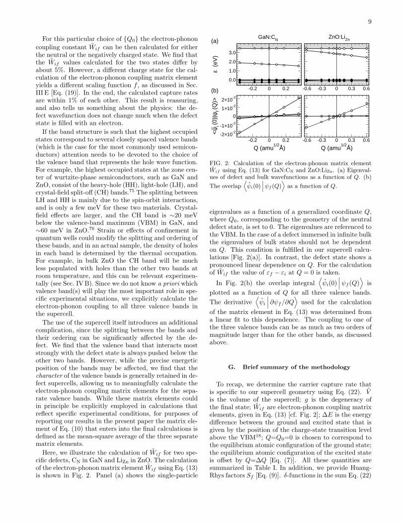
Here, we illustrate the calculation of Wif for two spe-cific defects, CN in GaN and LiZn in ZnO. The calculationof the electron-phonon matrix element Wif using Eq. (13)is shown in Fig. 2. Panel (a) shows the single-particle
-0.2 0 0.2
Q (amu1/2
Å)
-2×10⁻²
-1×10⁻²
0
1×10⁻²
2×10⁻²
<ψ
i (0)|
ψf (Q
)>
-0.2 0 0.2
0.0
1.0
2.0
3.0
ε (
eV)
-0.6 -0.3 0 0.3 0.6
Q (amu1/2
Å)
-0.6 -0.3 0 0.3 0.6
GaN:CNZnO:LiZn
~
(a)
(b)
FIG. 2: Calculation of the electron-phonon matrix elementWif using Eq. (13) for GaN:CN and ZnO:LiZn. (a) Eigenval-ues of defect and bulk wavefunctions as a function of Q. (b)
The overlap⟨
ψi(0)∣
∣
∣ψf (Q)⟩
as a function of Q.
eigenvalues as a function of a generalized coordinate Q,where Q0, corresponding to the geometry of the neutraldefect state, is set to 0. The eigenvalues are referenced tothe VBM. In the case of a defect immersed in infinite bulkthe eigenvalues of bulk states should not be dependenton Q. This condition is fulfilled in our supercell calcu-lations [Fig. 2(a)]. In contrast, the defect state shows apronounced linear dependence on Q. For the calculationof Wif the value of εf − εi at Q = 0 is taken.
In Fig. 2(b) the overlap integral⟨
ψi(0)∣∣∣ψf (Q)
⟩
is
plotted as a function of Q for all three valence bands.
The derivative⟨
ψi
∣∣∣ ∂ψf/∂Q
⟩
used for the calculation
of the matrix element in Eq. (13) was determined froma linear fit to this dependence. The coupling to one ofthe three valence bands can be as much as two orders ofmagnitude larger than for the other bands, as discussedabove.
G. Brief summary of the methodology
To recap, we determine the carrier capture rate thatis specific to our supercell geometry using Eq. (22). Vis the volume of the supercell; g is the degeneracy ofthe final state; Wif are electron-phonon coupling matrixelements, given in Eq. (13) [cf. Fig. 2]; ∆E is the energydifference between the ground and excited state that isgiven by the position of the charge-state transition levelabove the VBM18; Q=Q0=0 is chosen to correspond tothe equilibrium atomic configuration of the ground state;the equilibrium atomic configuration of the excited stateis offset by Q=∆Q [Eq. (7)]. All these quantities aresummarized in Table I. In addition, we provide Huang-Rhys factors Sf [Eq. (9)]. δ-functions in the sum Eq. (22)
10
are replaced by Gaussians with widths σ=0.8~Ωf .67
Finally, the actual carrier capture coefficient Cp is ob-
tained via Cp = fCp [Eq. (14)] with the scaling functionf . As discussed in Sec. III E, the calculation of f mayrequire a simulation in its own right; for the case of holecapture by a negatively charged defect, when the refer-ence system is that of the neutral charge state, we use theform Eq. (21) for f . This is the situation that occurs inthe examples of GaN:CN and ZnO:LiZn, to be discussedin Secs. IVA and IVB. For the case of hole capture bya neutral defect, which applies to GaN:(ZnGa-VN) to bediscussed in Sec. IVC, the reference system is that ofa positive charge state and f = 1.05 for our particularsupercell.
IV. RESULTS
To illustrate our methodology, we study two defectsin GaN, namely carbon on the nitrogen site (GaN:CN)and a complex of zinc on a gallium site with a nitro-gen vacancy (GaN:(ZnGa-VN)), as well as one defect inZnO, namely lithium on the zinc site (ZnO:LiZn). Exper-imental identification of defects is often very difficult andfrequently controversial. In order to check our methodol-ogy, we wanted to identify benchmark cases where the ex-perimental situation is clear-cut. GaN:CN and ZnO:LiZnserve this purpose.Although the focus is on nonradiative transitions, lu-
minescence experiments are frequently used to analyzerates of the various processes, radiative as well as non-radiative. There is general consensus that GaN:CN givesrise to a yellow luminescence band,36,78,79 and ZnO:LiZnto an orange luminescence band.37,66 These two bandsarise due to the recombination of an electron in the con-duction band and a hole bound to a defect. In both ofthese cases the acceptor level is in the lower part of theband gap.Nonradiative hole capture rates for deep acceptors can
be determined from luminescence experiments in the fol-lowing way.80 In n-type samples photo-generated holesare captured by acceptors in a predominantly nonradia-tive process (this conclusion stems from the fact that theresulting capture rates are orders of magnitude higherthan possible radiative capture rates, as discussed in Sec.II). Subsequently, these captured holes recombine withelectrons in the conduction band, a process believed tobe predominantly radiative, giving rise to the aforemen-tioned luminescence bands.80
When the temperature is increased, the radiative tran-sition is quenched because captured holes are re-emittedback into the valence band. Therefore, the measurementof the thermal quenching of a particular luminescenceband as a function of temperature provides informationabout the hole emission coefficient Qp. The parame-ters needed to determine Qp using this procedure arethe radiative lifetime τrad = 1/Cnn, measured separatelyfrom time-dependent photoluminescence decay, and the
quantum efficiency of the band with respect to all otherrecombination channels.80 The hole capture coefficientCp is determined from Qp using the detailed balanceequation.2,80 For acceptors in GaN and ZnO nonradia-tive hole capture coefficients determined in this way aresummarized in Ref.35.The GaN:(ZnGa-VN) defect, finally, has been included
in order to compare our approach to that of Ref. 25,where nonradiative hole capture at this defect was stud-ied.
A. CN in GaN
1. GaN:CN and yellow luminescence
Carbon is one of most abundant impurities in GaN,especially if grown by metal organic chemical vapor de-position, where organic precursors are used. A clear linkhas been established36,78 between the concentration ofcarbon and the intensity of a yellow luminescence (YL)band that peaks at about 2.2 eV. Contrary to earliersuggestions of carbon being a shallow acceptor, Lyons etal. have shown, using hybrid density functional calcula-tions, that carbon on the nitrogen site is in fact a deepacceptor.79 Calculations77,79,81 yield a (0/−) charge-statetransition level ∆E=0.9-1.1 eV above the VBM. In con-junction with a large lattice relaxation this correspondsto a peak very close to 2.2 eV for the optical transi-tion whereby a neutral defect captures an electron fromthe conduction band. Recently we have employed first-principles calculations to determine effective parameters(average phonon frequencies and the Huang-Rhys fac-tors, see Sec. III C and Table I) that describe the shapeand temperature dependence of luminescence bands. Inthe case of CN excellent agreement with experimentalresults35,36 was demonstrated.67
2. Configuration coordinate diagram
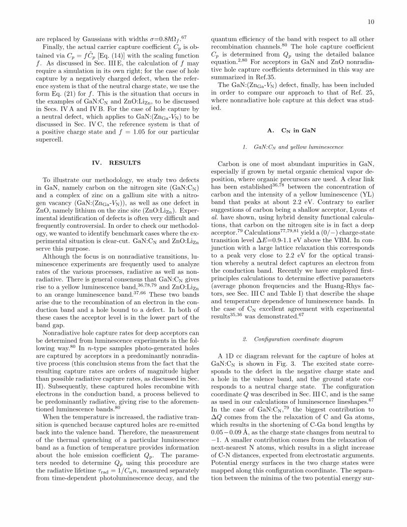
A 1D cc diagram relevant for the capture of holes atGaN:CN is shown in Fig. 3. The excited state corre-sponds to the defect in the negative charge state anda hole in the valence band, and the ground state cor-responds to a neutral charge state. The configurationcoordinate Q was described in Sec. III C, and is the sameas used in our calculations of luminescence lineshapes.67
In the case of GaN:CN,79 the biggest contribution to
∆Q comes from the the relaxation of C and Ga atoms,which results in the shortening of C-Ga bond lengths by0.05−0.09 A, as the charge state changes from neutral to−1. A smaller contribution comes from the relaxation ofnext-nearest N atoms, which results in a slight increaseof C-N distances, expected from electrostatic arguments.Potential energy surfaces in the two charge states weremapped along this configuration coordinate. The separa-tion between the minima of the two potential energy sur-
11
TABLE I: Key parameters for the three defects studied in this work: total mass-weighted distortions ∆Q [Eq. (7)], ionizationenergies ∆E, energies of effective vibrations ~Ωi,f [Eq. (8)] (charge state is given in parentheses), Huang-Rhys factors for the
final state [Eq. (9)], degeneracy factor g of the final state [cf. Eq. (4)), electron-phonon coupling matrix elements Wif [Eq. (13)and Fig. 2; the charge state of the defect for which the matrix element is calculated is shown in parentheses], and volume of
the supercell V in first-principles calculations.
∆Q (amu1/2A) ∆E (eV) ~Ωi (meV) ~Ωf (meV) Sf g Wif (eV/amu1/2A) V (A3)Defect theory expt.GaN:CN 1.61 1.02 (this work) 0.85a 42 (−) 36 (0) 10 4 6.4× 10⁻² (0) 1100ZnO:LiZn 3.22 0.80b, 0.49c, 0.46d 0.53e 36 (−) 25 (0) 28 4 3.9× 10⁻² (0) 1136GaN:(ZnGa-VN) 3.33 0.90f, 0.88 (this work) − 26 (0) 22 (+) 30 1 1.0 × 10⁻² (+) 1100
aRef.77bRef.64cRef.65dRef.66eRef.33fRef.25
-2 -1 0 1 2 3 4
Q (amu1/2
Å)
-0.5
0
0.5
1
1.5
2
ener
gy (
eV)
CN + h+
CN
∆Q
0∆E
_
GaN:CN
∆Erel
∆Eb
FIG. 3: (Color online) Calculated 1D cc diagram for hole cap-ture at the CN defect in GaN [process (1) in Fig. 1(b)]. Sym-bols: calculated values; solid line: parabolic fit. The defect inits negative charge state captures a hole, thus becoming neu-tral. ∆E is the energy difference between the minima of thetwo potential energy curves, ∆Erel is the relaxation energy inthe ground state, ∆Eb is the “classical” barrier for the nonra-diative process, and ∆Q is the displacement between the twopotential energy curves [Eq. (7)].
faces ∆E corresponds to the energy of the (0/−) charge-state transition level with respect to the VBM. Our cal-culated value for ∆E=1.02 eV is slightly larger than theone reported in Ref. 79 due to more stringent convergencecriteria. The minima of the two potential energy surfacesare offset horizontally by ∆Q=1.61 amu1/2A [Eq. (7)].An important parameter is the relaxation energy in theground state ∆Erel [Fig. 3]. For C0
N calculations yield∆Erel=0.37 eV.
The two potential energy curves intersect at ∆Eb=0.73eV above the minimum of the excited state. We mightthus expect that the nonradiative carrier capture is atemperature-activated process, since the coupling be-
tween two potential energy surfaces is always most ef-ficient close to the crossing point.3
3. Calculated hole capture coefficients
The real situation is not so straightforward becauseof the occurrence of two competing factors. On the onehand, when the temperature is raised, higher-lying vi-brational levels χim of the excited electronic state [seeEqs. (4) and (22)] become populated. Vibrational lev-els that are closer in energy to the crossing point of thetwo potential energy curves yield larger contributions tothe overall rate. Thus, if this was the only factor, thenonradiative capture rate for GaN:CN would increase asa function of temperature. On the other hand, however,the scaling factor f(T ) decreases with temperature, asper Eq. (21), because an increasingly faster hole has lesschance of being captured by a negative acceptor.It is instructive to consider the first effect separately.
In Fig. 4 we show the calculated nonradiative hole cap-ture rate if the second effect is completely neglected, i.e.,for f = 1. This is the capture rate Cp that is discussedin Section III E. The process is indeed temperature-activated. At high temperatures, the dependence is oftenfitted to a function of the form
Cp(T ) = C0 + C1exp(−∆E′b/kT ) (23)
with a temperature-independent part and a temperature-activated part. The use of such a form is at the core ofthe famous Mott-Seitz formula for temperature quench-ing of luminescence bands.3 The fit is shown in Fig. 4.From the fit one can derive an effective barrier ∆E′
b=0.23eV, which is significantly smaller than the “classical” bar-rier ∆Eb=0.73 eV. This is a typical result and happensbecause of the quantum-mechanical tunneling3 that isconsidered in the quantum treatment but absent in aclassical description.The actual hole capture coefficient, including the scal-
ing factor [Eq. (21)], is presented in Fig. 5 (solid black
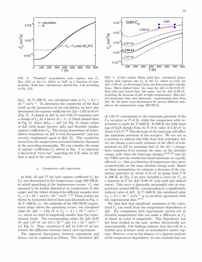
12
0 100 200 300 400 500 600 700 800T (K)
1×10⁻¹⁰
1×10⁻⁹
1×10⁻⁸
Cp (
cm3 /s
) calculationfit
C0 + C1exp(-∆Eb/kT)~
,
FIG. 4: “Nominal” nonradiative hole capture rate Cp
[Eq. (22)] at the CN defect in GaN as a function of tem-perature. Solid line: calculations; dotted line: a fit accordingto Eq. (23).
line). At T=300 K, our calculated value is Cp = 3.1 ×10⁻⁹ cm3s−1. To determine the sensitivity of the finalresult on the parameters of our calculation, we have alsodetermined the capture coefficient for ∆E=1.02±0.05 eV(Fig. 5). A change in ∆E by just 0.05 eV translates intoa change of Cp by a factor of ∼ 3− 4 (black dashed linesin Fig. 5). Since ∆Erel < ∆E (cf. Fig. 3), larger valuesof ∆E yield larger barriers ∆Eb and therefore smallercapture coefficients Cp. The strong dependence of nonra-diative transitions on ∆E is well documented,3 and wasrecently emphasized again in Ref. 25. This sensitivitystems from the temperature-activated behavior discussedin the preceding paragraphs. We can consider the rangeof capture coefficients Cp shown in Fig. 5 to representa theoretical “error bar” regarding the 0 K value of ∆Ethat is used in the calculation.
4. Comparison with experiment
In Refs. 35 and 77 the hole capture coefficient Cp forCN was determined in the temperature range 500-700 K,at which quenching of the luminescence occurs. Cp wasassumed to be weakly dependent on temperature in thisrange, and the values obtained for different samples wereCp = 3× 10⁻⁷ and 6× 10⁻⁷ cm3s−1.35 These results areshown by horizontal dotted lines and diamonds in Fig. 5.At T=600 K, i.e., the midpoint of the 500-700 K temper-ature range where the quenching occurs, our calculatedvalue for ∆E = 1.02 eV is Cp = 3.1 × 10⁻⁸ cm3s−1,i.e., about an order of magnitude smaller than the exper-imental result. The corresponding values for ∆E=0.97eV and 1.07 eV are 8.0 × 10⁻⁸ and 1.0 × 10⁻⁸ cm3s−1
(cf. Fig. 5). Thus, variations of ∆E by 0.05 eV do notremove the difference between theory and experiment.The apparent discrepancy between experiment and
theory can be explained as follows. The calculated ∆E
100 200 300 400 500 600 700 800T (K)
1×10⁻¹⁰
1×10⁻⁹
1×10⁻⁸
1×10⁻⁷
1×10⁻⁶
Cp (
cm3 /s
)
0.89 eV
* 1.02 eV
expt.GaN:CN
0.97 eV
1.07 eV
FIG. 5: (Color online) Black solid line: calculated nonra-diative hole capture rate Cp at the CN defect in GaN, for∆E=1.02 eV, as determined from our first-principles calcula-tions. Black dashed lines: the same for ∆E=1.02±0.05 eV.Red solid and dotted line: the same, but for ∆E=0.89 eV,modeling the decrease of ∆E at high temperatures. Blue dot-ted horizontal lines and diamonds: experimental data fromRef. 35; the latter were determined for several different sam-ples in the temperature range 500-700 K.
of 1.02 eV corresponds to the ionization potential of theCN acceptor at T=0 K, while the comparison with ex-periment is made for T≈600 K. At 600 K the bulk bandgap of GaN shrinks from its T=0 K value of 3.50 eV toabout 3.24 eV.30 This decrease of the band gap will affectthe ionization potential of the acceptor. We are not ina position to address this fully from first principles, butwe can obtain a zero-order estimate of the effect of tem-perature on ∆E by assuming that (i) the (0/−) charge-state transition level remains the same on the absoluteenergy scale when the band gap changes,43,81,82 and (ii)the VBM and the conduction-band minimum are equallyaffected, i.e., that as a function of temperature they movesymmetrically on the same absolute energy scale. Basedon these assumptions we estimate a decrease of the ion-ization potential by about 0.13 eV in going from 0 Kto 600 K. In Fig. 5 we have included a curve for Cp asa function of T for ∆E=0.89 eV (red solid and dashedcurve). This curve is physically meaningful only at tem-peratures around 600 K, corresponding to a significantlyreduced value of ∆E. At T=600 K, the calculated valueCp = 3.1 × 10⁻⁷ cm3s−1 is in excellent agreement withthe experimental data.35,77
We thus find that significant variations of the calcu-lated Cp can result from the temperature dependence of∆E. For comparison with experiments carried out atelevated temperatures this can make a difference in Cp
of about an order of magnitude. This dependence hasnot been studied in the past, neither theoretically norexperimentally. Our findings indicate that this will be afruitful area of future work on nonradiative carrier cap-ture. However, even in the absence of a rigorous analysisof the temperature dependence, we can conclude that our
13
calculated values of Cp are in very good agreement withexperimental data.
B. LiZn in ZnO
1. ZnO:LiZn and orange luminescence
LiZn in ZnO is one of the most studied defects in ZnO.While it was initially hoped that LiZn might be a shal-low acceptor leading to p-type doping, it is now clearthat this defect is a very deep acceptor. Meyer et al.
suggested that LiZn gives rise to a broad orange lumi-nescence (OL) band peaking at about 2.1 eV.37 The ion-ization energy was deduced to be at least 0.5 eV. Theanalysis based on the thermal quenching of luminescencelines confirms this and yields values for the ionizationpotential ∆E = 0.46 − 0.55 eV;33,35 the different val-ues are for different ZnO samples. Recent theoreticalwork based on the application of the generalized Koop-man’s theorem83 and on hybrid density functionals63–66
has confirmed that LiZn is indeed a deep acceptor witha ionization energy >0.3 eV. The neutral charge state ofthe defect corresponds to a small polaron bound to anoxygen atom that is adjacent to Li.
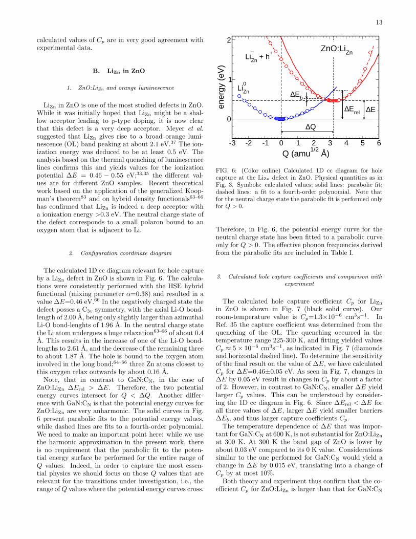
2. Configuration coordinate diagram
The calculated 1D cc diagram relevant for hole captureby a LiZn defect in ZnO is shown in Fig. 6. The calcula-tions were consistently performed with the HSE hybridfunctional (mixing parameter α=0.38) and resulted in avalue ∆E=0.46 eV.66 In the negatively charged state thedefect posses a C3v symmetry, with the axial Li-O bond-length of 2.00 A, being only slightly larger than azimuthalLi-O bond-lenghts of 1.96 A. In the neutral charge statethe Li atom undergoes a huge relaxation63–66 of about 0.4A. This results in the increase of one of the Li-O bond-lengths to 2.61 A, and the decrease of the remaining threeto about 1.87 A. The hole is bound to the oxygen atominvolved in the long bond;64–66 three Zn atoms closest tothis oxygen relax outwards by about 0.16 A.Note, that in contrast to GaN:CN, in the case of
ZnO:LiZn ∆Erel > ∆E. Therefore, the two potentialenergy curves intersect for Q < ∆Q. Another differ-ence with GaN:CN is that the potential energy curves forZnO:LiZn are very anharmonic. The solid curves in Fig.6 present parabolic fits to the potential energy values,while dashed lines are fits to a fourth-order polynomial.We need to make an important point here: while we usethe harmonic approximation in the present work, thereis no requirement that the parabolic fit to the poten-tial energy surface be performed for the entire range ofQ values. Indeed, in order to capture the most essen-tial physics we should focus on those Q values that arerelevant for the transitions under investigation, i.e., therange of Q values where the potential energy curves cross.
-3 -2 -1 0 1 2 3 4 5 6
Q (amu1/2
Å)
0
1
2
ener
gy (
eV)
LiZn + h+
LiZn
0
_
∆Q
∆E
ZnO:LiZn
∆Erel
∆Eb
FIG. 6: (Color online) Calculated 1D cc diagram for holecapture at the LiZn defect in ZnO. Physical quantities as inFig. 3. Symbols: calculated values; solid lines: parabolic fit;dashed lines: a fit to a fourth-order polynomial. Note thatfor the neutral charge state the parabolic fit is performed onlyfor Q > 0.
Therefore, in Fig. 6, the potential energy curve for theneutral charge state has been fitted to a parabolic curveonly for Q > 0. The effective phonon frequencies derivedfrom the parabolic fits are included in Table I.
3. Calculated hole capture coefficients and comparison with
experiment
The calculated hole capture coefficient Cp for LiZnin ZnO is shown in Fig. 7 (black solid curve). Ourroom-temperature value is Cp=1.3×10⁻⁶ cm3s−1. InRef. 35 the capture coefficient was determined from thequenching of the OL. The quenching occurred in thetemperature range 225-300 K, and fitting yielded valuesCp ≈ 5× 10⁻⁶ cm3s−1, as indicated in Fig. 7 (diamondsand horizontal dashed line). To determine the sensitivityof the final result on the value of ∆E, we have calculatedCp for ∆E=0.46±0.05 eV. As seen in Fig. 7, changes in∆E by 0.05 eV result in changes in Cp by about a factorof 2. However, in contrast to GaN:CN, smaller ∆E yieldlarger Cp values. This can be understood by consider-ing the 1D cc diagram in Fig. 6. Since ∆Erel < ∆E forall three values of ∆E, larger ∆E yield smaller barriers∆Eb, and thus larger capture coefficients Cp.The temperature dependence of ∆E that was impor-
tant for GaN:CN at 600 K, is not substantial for ZnO:LiZnat 300 K. At 300 K the band gap of ZnO is lower byabout 0.03 eV compared to its 0 K value. Considerationssimilar to the one performed for GaN:CN would yield achange in ∆E by 0.015 eV, translating into a change ofCp by at most 10%.Both theory and experiment thus confirm that the co-
efficient Cp for ZnO:LiZn is larger than that for GaN:CN
14
100 200 300 400 500 600 700T (K)
1×10⁻⁷
1×10⁻⁶
1×10⁻⁵
Cp (
cm3 /s
)
* 0.46 eV
expt.ZnO:LiZn
0.41 eV
0.51 eV
FIG. 7: (Color online) Solid black line: calculated nonradia-tive hole capture coefficient Cp at the LiZn defect in ZnO, for∆E=0.46 eV, as determined from our first-principles calcula-tions. Black dashed lines: the same, but for ∆E=0.46±0.05eV. Blue dashed lines and diamonds: experimental data fromRef. 33.
by about an order of magnitude. The main reason is thefact that the potential energy curves for ZnO:LiZn inter-sect close to the minimum of the excited state (Fig. 6),rendering the nonradiative process more likely even atlow temperatures. In addition, we find that the tem-perature dependence of Cp is significantly weaker forZnO:LiZn than in the case of GaN:CN. This is becausethe “classical” barrier ∆Eb for the nonradiative transi-tion is very small for ZnO:LiZn (Fig. 6).Overall, we can again conclude that first-principles cal-
culations of hole capture coefficients at ZnO:LiZn agreevery favorably with experimental data.
C. ZnGa-VN in GaN
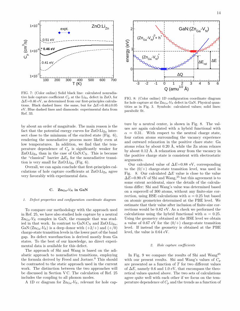
1. Defect properties and configuration coordinate diagram
To compare our methodology with the approach usedin Ref. 25, we have also studied hole capture by a neutralZnGa-VN complex in GaN, the example that was stud-ied in that work. In contrast to GaN:CN and ZnO:LiZn,GaN:(ZnGa-VN) is a deep donor with (+2/+) and (+/0)charge-state transition levels in the lower part of the bandgap. Its defect wavefunction is derived mostly from Gastates. To the best of our knowledge, no direct experi-mental data is available for this defect.The approach of Shi and Wang is based on the adi-
abatic approach to nonradiative transitions, employingthe formula derived by Freed and Jortner.8 This shouldbe contrasted to the static approach used in the currentwork. The distinction between the two approaches willbe discussed in Section VC. The calculation of Ref. 25includes the coupling to all phonon modes.A 1D cc diagram for ZnGa-VN, relevant for hole cap-
-3 -2 -1 0 1 2 3 4 5 6
Q (amu1/2
Å)
0
1
2
ener
gy (
eV) (ZnGa-VN) + h
+
(ZnGa-VN)+
0
∆Q
∆E
GaN:(ZnGa-VN)
∆Erel
FIG. 8: (Color online) 1D configuration coordinate diagramfor hole capture at the ZnGa-VN defect in GaN. Physical quan-tities as in Fig. 3. Symbols: calculated values; solid lines:parabolic fit.
ture by a neutral center, is shown in Fig. 8. The val-ues are again calculated with a hybrid functional withα = 0.31. With respect to the neutral charge state,four cation atoms surrounding the vacancy experienceand outward relaxation in the positive chare state: Gaatoms relax by about 0.20 A, while the Zn atom relaxesby about 0.12 A. A relaxation away from the vacancy inthe positive charge state is consistent with electrostaticarguments.Our calculated value of ∆E=0.88 eV, corresponding
to the (0/+) charge-state transition level, was used inFig. 8. Our calculated ∆E value is close to the value∆E=0.90 eV of Shi and Wang,25 but this agreement is tosome extent accidental, since the details of the calcula-tions differ: Shi and Wang’s value was determined basedon a supercell of 300 atoms, without any finite-size cor-rection, using HSE calculations with α = 0.25 but basedon atomic geometries determined at the PBE level. Weestimate that their value after inclusion of finite-size cor-rections would be 0.82 eV. As a check we performed thecalculations using the hybrid functional with α = 0.25.Using the geometry obtained at the HSE level we obtaina value of 0.67 eV for the (0/+) charge-state transitionlevel. If instead the geometry is obtained at the PBElevel, the value is 0.64 eV.
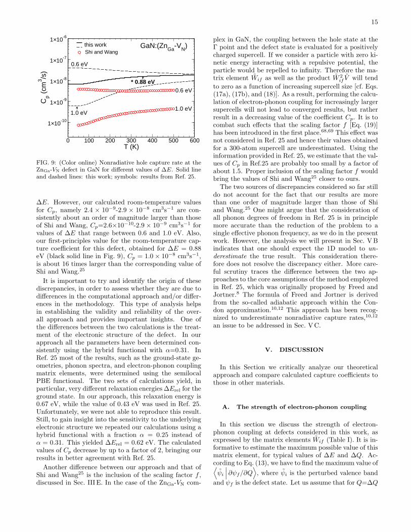
2. Hole capture coefficients
In Fig. 9 we compare the results of Shi and Wang25
with our present results. Shi and Wang’s values of Cp
are presented as a function of T for two different valuesof ∆E, namely 0.6 and 1.0 eV, that encompass the theo-retical values quoted above. The two sets of calculationsagree quite well with each other if we focus on the tem-perature dependence of Cp and the trends as a function of
15
0 100 200 300 400 500 600T (K)
1×10⁻¹⁰
1×10⁻⁹
1×10⁻⁸
1×10⁻⁷
1×10⁻⁶
Cp (
cm3 /s
) a aShi and Wang
GaN:(ZnGa-VN)
0.6 eV
1.0 eV
0.6 eV
1.0 eV
* 0.88 eV
this work
FIG. 9: (Color online) Nonradiative hole capture rate at theZnGa-VN defect in GaN for different values of ∆E. Solid lineand dashed lines: this work; symbols: results from Ref. 25.
∆E. However, our calculated room-temperature valuesfor Cp, namely 2.4 × 10⁻⁹-2.9 × 10⁻⁸ cm3s−1 are con-sistently about an order of magnitude larger than thoseof Shi and Wang, Cp=2.6×10⁻¹⁰-2.9 × 10⁻⁹ cm3s−1 forvalues of ∆E that range between 0.6 and 1.0 eV. Also,our first-principles value for the room-temperature cap-ture coefficient for this defect, obtained for ∆E = 0.88eV (black solid line in Fig. 9), Cp = 1.0 × 10⁻⁸ cm3s−1,is about 16 times larger than the corresponding value ofShi and Wang.25
It is important to try and identify the origin of thesediscrepancies, in order to assess whether they are due todifferences in the computational approach and/or differ-ences in the methodology. This type of analysis helpsin establishing the validity and reliability of the over-all approach and provides important insights. One ofthe differences between the two calculations is the treat-ment of the electronic structure of the defect. In ourapproach all the parameters have been determined con-sistently using the hybrid functional with α=0.31. InRef. 25 most of the results, such as the ground-state ge-ometries, phonon spectra, and electron-phonon couplingmatrix elements, were determined using the semilocalPBE functional. The two sets of calculations yield, inparticular, very different relaxation energies ∆Erel for theground state. In our approach, this relaxation energy is0.67 eV, while the value of 0.43 eV was used in Ref. 25.Unfortunately, we were not able to reproduce this result.Still, to gain insight into the sensitivity to the underlyingelectronic structure we repeated our calculations using ahybrid functional with a fraction α = 0.25 instead ofα = 0.31. This yielded ∆Erel = 0.62 eV. The calculatedvalues of Cp decrease by up to a factor of 2, bringing ourresults in better agreement with Ref. 25.
Another difference between our approach and that ofShi and Wang25 is the inclusion of the scaling factor f ,discussed in Sec. III E. In the case of the ZnGa-VN com-
plex in GaN, the coupling between the hole state at theΓ point and the defect state is evaluated for a positivelycharged supercell. If we consider a particle with zero ki-netic energy interacting with a repulsive potential, theparticle would be repelled to infinity. Therefore the ma-trix element Wif as well as the product W 2
if V will tend
to zero as a function of increasing supercell size [cf. Eqs.(17a), (17b), and (18)]. As a result, performing the calcu-lation of electron-phonon coupling for increasingly largersupercells will not lead to converged results, but ratherresult in a decreasing value of the coefficient Cp. It is tocombat such effects that the scaling factor f [Eq. (19)]has been introduced in the first place.68,69 This effect wasnot considered in Ref. 25 and hence their values obtainedfor a 300-atom supercell are underestimated. Using theinformation provided in Ref. 25, we estimate that the val-ues of Cp in Ref.25 are probably too small by a factor ofabout 1.5. Proper inclusion of the scaling factor f wouldbring the values of Shi and Wang25 closer to ours.The two sources of discrepancies considered so far still
do not account for the fact that our results are morethan one order of magnitude larger than those of Shiand Wang.25 One might argue that the consideration ofall phonon degrees of freedom in Ref. 25 is in principlemore accurate than the reduction of the problem to asingle effective phonon frequency, as we do in the presentwork. However, the analysis we will present in Sec. VBindicates that one should expect the 1D model to un-
derestimate the true result. This consideration there-fore does not resolve the discrepancy either. More care-ful scrutiny traces the difference between the two ap-proaches to the core assumptions of the method employedin Ref. 25, which was originally proposed by Freed andJortner.8 The formula of Freed and Jortner is derivedfrom the so-called adiabatic approach within the Con-don approximation.10,12 This approach has been recog-nized to underestimate nonradiative capture rates,10,12
an issue to be addressed in Sec. VC.
V. DISCUSSION
In this Section we critically analyze our theoreticalapproach and compare calculated capture coefficients tothose in other materials.
A. The strength of electron-phonon coupling
In this section we discuss the strength of electron-phonon coupling at defects considered in this work, asexpressed by the matrix elements Wif (Table I). It is in-formative to estimate the maximum possible value of thismatrix element, for typical values of ∆E and ∆Q. Ac-cording to Eq. (13), we have to find the maximum value of⟨
ψi
∣∣∣ ∂ψf/∂Q
⟩
, where ψi is the perturbed valence band
and ψf is the defect state. Let us assume that for Q=∆Q
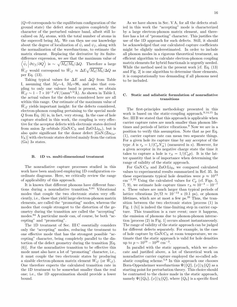
16
(Q=0 corresponds to the equilibrium configuration of theground state) the defect state acquires completely thecharacter of the perturbed valence band, albeit still lo-calized on Md atoms, with the total number of atoms inthe supercell being Mb. We can then use our knowledgeabout the degree of localization of ψi and ψf , along withthe normalization of the wavefunctions, to estimate thematrix element. Replacing the derivative by its finite-difference expression, we see that the maximum value of⟨
ψi
∣∣∣ ∂ψf/∂Q
⟩
is ∼√
Md/Mb/∆Q. Therefore a large
Wif would correspond to Wif ≈ ∆E√
Md/Mb/∆Q asper Eq. (13).Taking typical values for ∆E and ∆Q from Table
I, assuming that Md∼4, Mb=96, and also that cou-pling to only one valence band is present, we obtainWif ∼ 1− 7× 10⁻² eV/(amu1/2A). As shown in Table I,the actual values for the defects considered here are allwithin this range. Our estimate of the maximum value ofWif yields important insight: for the defects considered,electron-phonon coupling pertaining to the special modeQ from Eq. (6) is, in fact, very strong. In the case of holecapture studied in this work, the coupling is very effec-tive for the acceptor defects with electronic states derivedfrom anion 2p orbitals (GaN:CN and ZnO:LiZn), but isalso quite significant for the donor defect [GaN:(ZnGa-VN)] with electronic states derived mainly from the cation(Ga) 3s states.
B. 1D vs. multi-dimensional treatment
The nonradiative capture processes studied in thiswork have been analyzed employing 1D configuration co-ordinate diagrams. Here, we critically review the rangeof applicability of this approach.It is known that different phonons have different func-
tions during a nonradiative transition.8,84 Vibrationalmodes that couple the two electronic states very effi-ciently, i.e., those that yield large electron-phonon matrixelements, are called the “promoting” modes, whereas themodes that couple strongest to the distortion of the ge-ometry during the transition are called the “accepting”modes.84 A particular mode can, of course, be both “ac-cepting” and “promoting”.The 1D treatment of Sec. III C essentially considers
only the “accepting” modes, reducing the treatment toone effective mode that has the strongest possible “ac-cepting” character, being completely parallel to the dis-tortion of the defect geometry during the transition [Eq.(6)]. For the nonradiative transition to be effective thismode must also have a lot of “promoting” character, i.e.,it must couple the two electronic states by producinga sizable electron-phonon matrix element Wif (or Wif ).One therefore expects the calculated transition rate inthe 1D treatment to be somewhat smaller than the realone; i.e., the 1D approximation should provide a lowerbound.
As we have shown in Sec. VA, for all the defects stud-ied in this work the “accepting” mode is characterizedby a large electron-phonon matrix element, and there-fore has a lot of “promoting” character. This justifies theuse of the 1D approach for such defects. Still, it shouldbe acknowledged that our calculated capture coefficientsmight be slightly underestimated. In order to includeall phonon modes in a rigorous theoretical treatment, anefficient algorithm to calculate electron-phonon couplingmatrix elements for hybrid functionals is urgently needed.While the method used in the present work [cf. Eq. (13)and Fig. 2] is one algorithm to determine those elements,it is computationally too demanding if all phonons needto be included.
C. Static and adiabatic formulation of nonradiative
transitions
The first-principles methodology presented in thiswork is based on the static-coupling approach.9,14,15 InSec. III B we stated that this approach is applicable whencarrier capture rates are much smaller than phonon life-times and periods of lattice vibrations.9 Now we are in aposition to verify this assumption. Note that as per Eq.(1), carrier capture rate can mean two separate things.For a given hole its capture time by any acceptor of thetype A is τp = 1/(CpN
−A ) (measured in s). However, for
a given acceptor in its negative charge state the time ittakes to capture a hole is τA = 1/(Cpp). It is the lat-ter quantity that is of importance when determining therange of validity of the static approach.For GaN:CN and ZnO:LiZn we compared calculated
values to experimental results summarized in Ref. 35. Inthese experiments typical hole densities were p ≈ 1013
cm−3.32 Using the calculated values for Cp (cf. Figs. 5,7, 9), we estimate hole capture times τA ≈ 10−4 − 10−7
s. These values are much larger than typical periods oflattice vibrations 2π/Ω ≈ 10−13 s (0.1 ps), or phononlifetimes, which are at most a few ps.39 Thus, the tran-sition between the two electronic states [process (1) inFig. 1 (b)] is indeed the time-limiting step in carrier cap-ture. This transition is a rare event; once it happens,the emission of phonons due to phonon-phonon interac-tion [process (2) in Fig. 1] occurs almost instantaneously.The range of validity of the static approach can be judgedfor different defects separately. For example, in the caseof hole capture by GaN:CN at room temperature, we es-timate that the static approach is valid for hole densitiesup to p ∼ 1019 − 1020 cm−3.In parallel with the static approach, which we advo-
cate and justified above, a lot of theoretical work onnonradiative carrier capture employed the so-called adi-abatic coupling scheme.5,8 In this approach one choosesBorn-Oppenheimer wavefunctions Ψ(Q, x)χQ as astarting point for perturbation theory. This choice shouldbe contrasted to the choice made in the static approach,namely Ψ(Q0, x)χQ, where Q0 is a specific fixed
17
atomic configuration (see Sec. III B). Many early formu-lations based on the adiabatic approach also assumedthat electron-phonon matrix elements were independentof Q,5,8 which is the Condon approximation for nonra-diative transitions. However, already in the 1970s it wasnoticed that the adiabatic approach within the Condonapproximation yielded capture rates significantly smallerthan the static approach applied to the same system.9
This result was very surprising at the time; indeed, itwas expected that far from the intersection of potentialenergy surfaces the two descriptions should yield verysimilar physics.
The issue was resolved in the early 1980s by Huang,10
Gutsche and co-workers,11,12 and Burt.13 The discrep-ancy was found to originate in an inconsistent applica-tion of the adiabatic approach. These authors demon-strated that within the leading order the adiabatic ap-proach does give the same answer as the static approach,provided the adiabatic approach is applied consistently.This can be achieved in one of two ways: (i) by go-ing beyond the Condon approximation in the adiabatictreatment10; or (ii) by considering all non-diagonal termsin the Hamiltonian.12 In particular, erroneous omissionof non-diagonal terms can lead to significantly smallervalues of capture rates in the adiabatic approach.12 Thiswas exactly the problem of prior theoretical treatmentsthat were based on the adiabatic approach together withthe Condon approximation.5,8
The discussion up to this point applies to the casewhere nonradiative transitions occur far from the inter-section of two potential energy surfaces. However, whentransitions close to the crossing point are important (asis the case for ZnO:LiZn and GaN:CN, cf. Figs. 6 and8) the adiabatic approach within the Condon approxi-mation fails altogether. In the adiabatic approach, anavoided crossing occurs between the two potential en-ergy surfaces, leading to a strong variation of electronicwavefunctions and making potential energy surfaces veryanharmonic. In such a situation, adiabatic wavefunctionsare probably not a good starting point for perturbationtheory.9 The static coupling scheme, on the other hand,is still applicable in the regime close to the intersectionof the potential energy surfaces.9,14
In our opinion, the application of the adiabatic cou-pling scheme in Ref. 25, versus the static scheme em-ployed in the present work, is the major reason for thedifferences between our results and those of Ref. 25 (Fig.9). The results of Ref. 25 were obtained based on theformula of Freed and Jortner,8 which uses the adiabaticcoupling scheme within the Condon approximation andwill thus tend to underestimate the values for capturecoefficients.10–13
The theoretical foundations of nonradiative capturedue to multi-phonon emission were laid in Refs. 4–15. References 10–13, in particular, contain impor-tant lessons about the proper application of various ap-proaches. Unfortunately, activity in this field stagnated,partly due to the difficulty of obtaining sufficiently accu-
rate results with the computational methods that wereavailable at the time. The current power of accurate elec-tronic structure methods creates a fertile environment inwhich to achieve the goal of a quantitative determinationof carrier capture rates completely from first principles.This analysis, which finds its roots in similar discus-
sions of 1970s and 1980s, relates to the underlying the-ory to describe nonradiative capture and does not under-mine the achievements of Ref. 25. Most importantly, inRef. 25 a new efficient algorithm to calculate electron-phonon coupling was proposed. The algorithm considersall phonon degrees of freedom and can be in principleused also in conjunction with the static approach used inthe current work. A further extension of the algorithmto hybrid functionals is currently highly desirable.
D. Comparison with other materials
It is instructive to compare our results of capture coef-ficients to those in other materials. However, one shouldkeep in mind that for any given defect the resulting cap-ture rate depends on many parameters, including: (i)details of the cc diagram, for example “classical” barri-ers for nonradiative capture ∆Eb (cf. Figs. 3, 6, 8); (ii)the strength of electron-phonon coupling [Eqs. (4) and(22)]; (iii) the charge state of the defect [cf. Eqs. (14) and(21)]; (iv) temperature. Furthermore, many experimen-tal papers report capture cross sections σ rather thancapture coefficients C. As discussed in Sec. II, the twoare related via C = 〈v〉σ, where 〈v〉 is a characteristiccarrier velocity. In the case of non-degenerate carrierstatistics the characteristic velocity is the average ther-mal velocity 〈v〉 ∼
√T , which introduces an additional
temperature-dependent prefactor in the expression for σ.These considerations indicate that the comparison of car-rier capture characteristics of different defects in differentmaterials should be approached with caution. However,some conclusions can still be drawn.Let us consider a specific material, and look at carrier
capture cross sections for a wide range of defects. Thosecross sections will depend on the specific defect, as wellas on temperature. However, one could argue that themaximum value of capture cross section across all defectsand across all temperature ranges (say, for temperatureswhere non-degenerate carrier statistics apply), would beindicative of the strength of electron-phonon coupling inthe host material.In their seminal paper, Henry and Lang studied cap-
ture cross sections at defects in GaP and GaAs.4 Themeasurements were performed by deep-level transientspectroscopy over the temperature range 100-600 K, com-parable to the temperature range discussed in the presentwork. Both electron and hole capture was studied. Cap-ture cross sections at various defects ranged from 10−5
to about 100 A2 for these temperatures. One could cau-tiously conclude that ∼100 A2 is the maximum capturecross section for any defect system in GaP and GaAs.
18
For the three defects studied in the present work, cal-culated hole capture cross sections vary from 0.1 to 200A2 in GaN (Figs. 5 and 9), and from 1000 to 2000 A2
in ZnO (Fig. 7) for a similar temperature range. In par-ticular, we find σ = 180 A2 in GaN:CN at T=600 K, andσ = 1000 A2 for ZnO:LiZn at T = 225 K. As discussed inSec. IV, these results are in agreement with the exper-imental data of Ref. 35. While our data set is limited,it is clear that carrier capture cross sections in ZnO andGaN tend to be larger than those in GaP and GaAs. Weattribute this to the larger strength of electron-phononinteractions in wide-band-gap materials such as GaN andZnO, compared to GaP and GaAs. This strength directlyaffects the matrix elements, as discussed in Sec. VA.These trends for nonradiative capture at defects are
in accord with the knowledge of electron-phonon inter-actions in bulk solids. Let us take the interaction of freecarriers with longitudinal optical (LO) phonons as an ex-ample. This strength of this interaction can be charac-terized by a dimensionless factor, the Frohlich parameterαF = e2/~
√
m/(2~ωLO)(1/ε∞ − 1/ε0) (in SI units).85
For holes, αF ≈ 0.15 in GaAs and αF ≈ 0.2 in GaP,while αF is about 1.0 in GaN and 1.5 in ZnO, indeedindicative of stronger interaction.
VI. CONCLUSIONS
In conclusion, we have developed a first-principlesmethodology to study nonradiative carrier capture bymeans of multiphonon emission at defects in semiconduc-tors. All the parameters, including the electron-phononcoupling, have been determined consistently using hybriddensity functional calculations, which yield accurate bulkband structures as well as defect properties. Significantsimplifications occur due to the implementation of a 1Dmodel, for which we provided extensive justification, andwhich also yields useful insights into the defect physics.
We applied our methodology to several hole-capturingcenters in GaN and ZnO. The resulting capture coef-ficients are large, and in agreement with experimentaldata. We conclude that state-of-the-art electronic struc-ture techniques, when combined with reliable method-ological approaches, are capable of accurately describingcarrier capture processes. The methodology thus allowsgenerating reliable information for defects for which ex-perimental information is incomplete—which seems tobe the case for the majority of defects that are poten-tially relevant for charge trapping or SRH recombinationin semiconductor devices. The combination of a first-principles approach with experiment can also be a pow-erful aid in the identification of defects. Finally, our first-principles approach allows making predictions for newmaterials for which no experimental data is as yet avail-able.
Acknowledgements
We acknowledge M. A. Reshchikov for valuable inter-actions and providing us with a preprint of Ref. 35. Wealso thank L. Shi and L.-W. Wang for sharing their datafor GaN:(ZnGa − VN), A. Carvalho for providing the Lipseudopotential, and C. E. Dreyer, F. Giustino, A. Jan-otti, J. L. Lyons, J. S. Speck, S. Keller, and C. Weis-buch for fruitful discussions. A.A. was supported bythe Office of Science of of the U.S. Department of En-ergy (Grant No. de-sc0010689), and by the Swiss NSF(PA00P2 134127) during the initial phase of the project.Q.Y. was supported by the UCSB Solid State Lightingand Energy Center. Computational resources were pro-vided by the National Energy Research Scientific Com-puting Center, which is supported by the DOE Office ofScience under Contract No. DE-AC02-05CH11231, andby the Extreme Science and Engineering Discovery En-vironment (XSEDE), supported by NSF (OCI-1053575and NSF DMR07-0072N).
1 U. K. Mishra, P. Parikh, and Y.-F. Wu, Proc. IEEE 90,1022 (2002).
2 V. N. Abakumov, V. I. Perel’, and I. N. Yassievich,Nonradiative Recombinations in Semiconductors (North-Holland, Amsterdam, 1991).
3 B. Di Bartolo (ed.), Advances in Nonradiative Processes in
Solids (Plenum Press, New York, 1991).4 C. H. Henry and D. V. Lang, Phys. Rev. B 15, 989 (1977).5 K. Huang and A. Rhys, Proc. Royal Soc. 204, 406 (1950).6 R. Kubo and I. Toyozawa, Prog. Theor. Phys. 13, 160(1955).
7 H. Gummel and M. Lax, Annals of Phys. 2, 28 (1957).8 K. F. Freed and J. Jortner, J. Chem. Phys. 52, 6272 (1970).9 R. Passler, Phys. Status Solidi (b) 68, 69 (1975).
10 K. Huang, Scientia Sinica 14, 27 (1981).11 E. Gutsche, Phys. Status Solidi 109, 583 (1982).12 K. Peuker, R. Enderlein, A. Schenk, and E. Gutsche, Phys.
Status Solidi 109, 599 (1982).
13 M. G. Burt, J. Phys. C: Solid State Phys. 16, 4137 (1983).14 R. Passler, Czech. J. Phys. 32, 846 (1982).15 D. Goguenheim and M. Lannoo, J. Appl. Phys. 68, 1059
(1990).16 A. M. Stoneham, Theory of Defects in Solids (Oxford Uni-
versity Press, 1975).17 W. H. Strehlow and E. L. Cook, J. Phys. Chem. Ref. Data
2, 163 (1973).18 C. Freysoldt, B. Grabowski, T. Hickel, J. Neugebauer, G.
Kresse, A. Janotti, and C. G. Van de Walle, Rev. Mod.Phys. 86, 253 (2014).
19 Theory of Defects in Semiconductors, edited by D. A.Drabold and S. Estreicher (Springer, 2007).
20 Advanced Calculations for Defects in Materials, edited byA. Alkauskas, P. Deak, J. Neugebauer, A. Pasquarello, andC. G. Van de Walle (Wiley, Weinheim, 2011).
21 F. Schanovsky, W. Gos, and T. Grasser, J. Vac. Sci. Tech-nol. B 29, 01A201 (2011).
19
22 F. Schanovsky, O. Baumgartner, V. Sverdlov, and T.Grasser, J. Comput. Electron. 11, 218 (2012).
23 K. P. McKenna and J. Blumberger, Phys. Rev. B 86,245110 (2012).
24 R. A. Marcus, Rev. Mod. Phys. 65, 599 (1993).25 L. Shi and L.-W. Wang, Phys. Rev. Lett. 109, 245501
(2012).26 M. A. Reshchikov, A. A. Kvasov, M. F. Bishop, T. Mc-
Mullen, A. Usikov, V. Soukhoveev, and V. A. Dmitriev,Phys. Rev. B 84, 075212 (2011).
27 S. Baroni, S. de Gironcoli, and A. Dal Corso, Rev. Mod.Phys. 73, 515 (2001).
28 F. Giustino, M. L. Cohen, and S. G. Louie, Phys. Rev. B76, 165108 (2007).
29 R. Borrelli and A. Peluso, J. Chem. Phys. 119, 8437(2003).
30 N. Nepal, J. Li, M. L. Nakarmi, J. Y. Lin, and H. X. Jiang,Appl. Phys. Lett. 87, 242104 (2005).
31 D. C. Reynolds, D. C. Look, B. Jogai, C. W. Litton, G.Cantwell, and W. C. Harsch, Phys. Rev. B 60, 2340 (1999)
32 M. A. Reshchikov and H. Morkoc, J. Appl. Phys. 97,061301 (2005).
33 M. A. Reshchikov, H. Morkoc, B. Nemeth, J. Nause, J.Xie, B. Hertog, and A. Osinsky, Physica B 401-402, 358(2007).
34 M. A. Reshchikov, J. Garbus, G. Lopez, M. Ruchala, B.Nemeth, and J. Nause, Mater. Res. Soc. Symp. Proc. 957,0957-K07-19 (2007).
35 M. A. Reshchikov, AIP Conf. Proc. 1583, 127 (2014).36 T. Ogino and M. Aoki, Jap. J. Appl. Phys. 19, 2395 (1980).37 B. K. Meyer, H. Alves, D. M. Hofmann, W. Kriegsies, D.
Forster, F. Bertram, J. Christen, A. Hoffmann, M. Strass-burg, M. Dworzak, U. Haboeck, and A. V. Rodina, Phys.Status Solidi B 241, 231 (2004)
38 J. L. Lyons, A. Janotti, and C. G. Van de Walle, Appl.Phys. Lett. 97, 1521088 (2009).
39 A. Matulionis, J. Liberis, I. Matulioniene, M. Ramonas,E. Sermuksnis, J. H. Leach, M. Wu, X. Ni, X. Li, and H.Morkoc, Appl. Phys. Lett. 95, 192102 (2009).
40 J. Heyd, G. E. Scuseria, and M. Ernzerhof, J. Chem. Phys.118, 8207 (2003); ibid. 124, 219906 (2006).
41 G. Pacchioni, F. Frigoli, D. Ricci, and J. A. Weil, Phys.Rev. B 63, 054102 (2000).
42 P. Deak, A. Gali, A. Solyom, A. Buruzs, and Th. Frauen-heim, J. Phys.: Condens. Mat. 17, S2141 (2005).
43 A. Alkauskas, P. Broqvist, and A. Pasquarello, Phys. Rev.Lett. 101, 046405 (2008); Phys. Status Solidi B 248, 775(2011).
44 J. L. Lyons, A. Janotti, and C. G. Van de Walle, Phys.Rev. Lett. 108, 156403 (2012).
45 J. L. Lyons, A. Janotti, and C. G. Van de Walle, Jap. J.Appl. Phys. 52, 08JJ04 (2013).
46 J. P. Perdew, K. Burke, and M. Ernzerhof, Phys. Rev.Lett. 77, 3865 (1996).
47 P. E. Blochl, Phys. Rev. B 50, 17953 (1994).48 G. Kresse and J. Furthmuller, Phys. Rev. B 54, 11169
(1996); G. Kresse and D. Joubert, Phys. Rev. B 59, 1758(1999).
49 J. Paier, M. Marsman, K. Hummer, G. Kresse, I. C. Ger-ber, amd J. G. Angyan, J. Chem. Phys. 124, 154709(2006).
50 Semiconductors: Basic Data, 2nd ed., edited by O.Madelung (Springer, Berlin, 1996).
51 C. Freysoldt, J. Neugebauer, and C. G. Van de Walle,
Phys. Rev. Lett. 102, 016402 (2009); Phys. Status Sol.B 248, 1067 (2011).
52 A. Baldereschi, Phys. Rev. B 7, 5212 (1973).53 J. Ihm, A. Zunger, and M.-L. Cohen, J. Phys. C: Solid
State Phys. 12, 4409 (1979).54 N. Troullier and J. L. Martins, Phys. Rev. B 43, 1993
(1991).55 M. Fuchs and M. Scheffler, Comput. Phys. Commun. 119,
67 (1999).56 CPMD, Copyright IBM Corp 1990-2006, Copyright MPI
fur Festkorperforschung Stuttgart 1997-2001; J. Hutterand A. Curioni, ChemPhysChem 6, 1788 (2005).
57 T. Todorova, A. P. Seitsonen, J. Hutter, I. F. W. Kuo, andC. J. Mundy, J. Phys. Chem. B 110, 3685 (2006).
58 P. Broqvist, A. Alkauskas, and A. Pasquarello, Phys. Rev.B 80, 085114 (2009).
59 H.-P. Komsa, P. Broqvist, and A. Pasquarello, Phys. Rev.B 81, 205118 (2010).
60 A. Alkauskas, P. Broqvist, F. Devynck, and A. Pasquarello,Phys. Rev. Lett. 101, 106802 (2008).
61 X. Wu, E. J. Walter, A. M. Rappe, R. Car, and A. Selloni,Phys. Rev. B 80, 115201 (2009).
62 L. Hedin and S. Lundqvist, in Solid State Physics (Ed. F.Seitz, D. Turnbull and H. Ehrenreich), Vol. 23, 1 (1970)
63 M.-H. Du and S.-B. Zhang, Phys. Rev. B 80, 115217(2009).
64 A. Carvalho, A. Alkauskas, A. Pasquarello, A. K. Tagant-sev, and N. Setter, Phys. Rev. B 80, 195205 (2009).
65 T. S. Bjørheim, S. Erdal, K. M. Johansen, K. E. Knutsen,and T. Norby, J. Phys. Chem. C 116, 23764 (2012).
66 J. L. Lyons, A. Janotti, and C. G. Van de Walle, in prepa-ration (2014).
67 A. Alkauskas, J. L. Lyons, D. Steiauf, and C. G. Van deWalle, Phys. Rev. Lett. 109, 267401 (2012).
68 V. L. Bonch-Bruevich, Fiz. Tverd. Tella, Sbornik II, 182(1959).
69 R. Passler, Phys. Status Solidi B 78, 625 (1976).70 W. Kohn, Phys. Rev. 105, 509 (1957).71 L. D. Landau and L. M. Lifshitz, Quantum Mechanics.
Non-relativistic theory (Butterworth-Heinemann, 1981).72 J. J. Pankove, S. Bloom, and G. Harbecke, RCA Rev. 36,
163 (1975).73 B. Santic, Semicond. Sci. Technology 18, 219 (2003)74 K. Hummer, Phys. Status Solidi (b) 56, 249 (1973).75 I. Vurgaftman and J. R. Meyer, chapter 2 in Nitride Semi-
conductor Devices, Ed. J. Piprek, (Wiley-VCH, 2007).76 Q. Yan, P. Rinke, M. Winkelnkemper, A. Qteish, D. Bim-
berg, M. Scheffler, and C. G. Van de Walle, Semicond. Sci.Technol. 26, 014307 (2011).
77 D. O. Demchenko, I. C. Diallo, and M. A. Reshchikov,Phys. Rev. Lett. 110, 087404 (2013).
78 C. H. Seager, D. R. Tallant, J. Yu, and W. Gotz, J. ofLumin. 106, 115 (2004).
79 J. L. Lyons, A. Janotti, and C. G. Van de Walle, Appl.Phys. Lett. 97, 152108 (2010).
80 M. A. Reshchikov, in Photoluminescence: Applications,
Types and Efficacy, Ed. M. A. Case and B. C. Stout (NovaScience, New York, 2012).
81 J. L. Lyons, A. Janotti, and C. G. Van de Walle, Phys.Rev. B 89, 035204 (2014).
82 W. Chen and A. Pasquarello, Phys. Rev. B 88, 115104(2013).
83 S. Lany and A. Zunger, Phys. Rev. B 80, 085202 (2009).84 A. M. Stoneham, Rep. Prog. Phys. 44, 1251 (1981).
20
85 See, e.g., p. 62 of B. K. Ridley, Quantum Processes in
Semiconductors (Clarendon Press, 1999).


![TheUcenterandthepoint-ionmethodhalogenuros alcalinos que110 habían sido considerados. Losvalores obtenidos secomparan con los queseoblienen delaleyde¡vey[21]. PACS: 61.70.-r; 71.55.-i;](https://static.fdocuments.us/doc/165x107/6010ece791b7fe76ac2f7e13/theucenterandthepoint-ionmethod-halogenuros-alcalinos-que110-haban-sido-considerados.jpg)