Packaging Technologies for Flash Memory - SEMICON … · JCET Confidential Significant...
23
Packaging Technologies for Flash Memory Steve X. Liang, SVP/CTO 3/2017@Semicon China, Shanghai
Transcript of Packaging Technologies for Flash Memory - SEMICON … · JCET Confidential Significant...

Packaging Technologies for Flash Memory
Steve X. Liang, SVP/CTO
3/2017@Semicon China, Shanghai
JCET Confidential
• Worldwide Semiconductor and Memory
• China’s Memory Industry Growth
• 2D to 3D NAND Ramping-Up
• Packaging Technologies for Memory
• JCET Memory Packaging Portfolio
2

JCET Confidential
Global Semiconductor and Memory Market
Memory Contributes To One-fourth Of World Wide Semiconductor Consumption
Source : Micron / Gartner 4Q15
3
2015
JCET Confidential
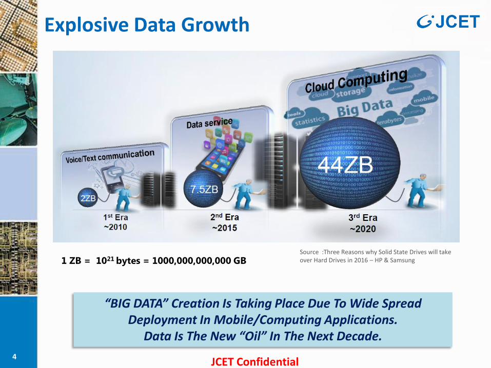
Explosive Data Growth
1 ZB = 1021 bytes = 1000,000,000,000 GB
“BIG DATA” Creation Is Taking Place Due To Wide Spread Deployment In Mobile/Computing Applications.
Data Is The New “Oil” In The Next Decade.
Source :Three Reasons why Solid State Drives will take over Hard Drives in 2016 – HP & Samsung
4
JCET Confidential
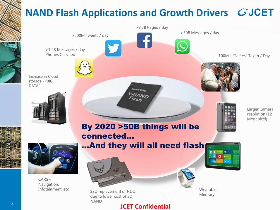
NAND Flash Applications and Growth Drivers
5
>50B Messages / day
>8.7B Pages / day
>500M Tweets / day
>1.2B Messages / day
Phones Checked 100M+ “Selfies” Taken / Day
Larger Camera
resolution (12
Megapixel)
Wearable
Memory
Increase in Cloud
storage - “BIG
DATA”
By 2020 >50B things will be
connected…
…And they will all need flash
SSD replacement of HDD
due to lower cost of 3D
NAND
CARS –
Navigation,
Infotainment, etc

JCET Confidential
China’s Memory Consumptions
6 Source : TrendForce, Oct 2015
Chinese Domestic DRAM And NAND Flash Consumption Is Dramatically Increasing With The Rise Of PCs Smartphones. China Consume ~ 30% Of World’s Memory Production And
Most Of Them Are Imported

JCET Confidential
China’s NAND Flash Significant Growth
7
Source : Trendforce, Apr 2016

JCET Confidential
Memory Device Technology Advance
8
2004 2006 2008 2010 2012 2014 2016 2002 2000 2020 2018
130nm 128 MB 90nm
512 MB 50nm 1 GB
34nm 4 GB
25nm 8 GB
16nm 16 GB
3D (48L) 32 GB
INTEL NAND Wafer node scaling
SAMSUNG NAND Wafer node scaling
Planar NAND
120nm 128 MB
90nm 256 MB
70nm 512 MB
60nm 1 GB
50nm 2 GB
40nm 4 GB
19nm 16 GB
3D NAND 32 GB
3D NAND
2022
Emerging
24L 48L 72L 3D ReRAM
3D NAND Technology Provides Economic Benefits Of Scaling Significantly Drive Down $/Bit Cost
JCET Confidential
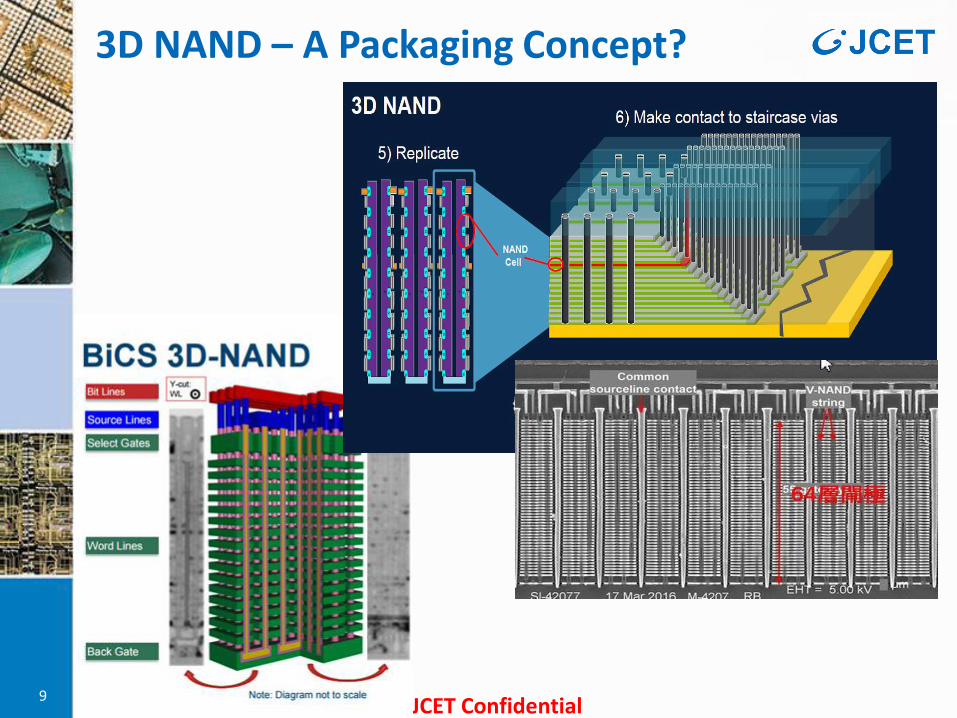
3D NAND – A Packaging Concept?
9
JCET Confidential
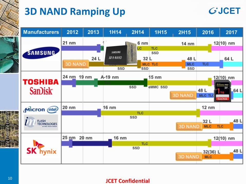
3D NAND Ramping Up
10

JCET Confidential
11
Memory and NAND Packaging
SD -SiP
MicroSD
USB-SiP
eMCP
eMMC
REMOVABLE MOBILE / WEARABLE CLIENT SSD ENTERPRISE SSD AUTOMOTIVE
FBGA-SD
UFS
FLIP CHIP (SSD Controller)
Single chip eWLB
TSOP
TSOP
SD -SiP
MicroSD
G
G FBGA-SD

JCET Confidential
Overview of JCET Group
12
Founded in 1972 and listed on Shanghai Stock Exchange in 2003
Significant manufacturing scale with factories strategically located in China, Singapore and Korea
Experienced R&D team driving innovations in advanced technologies with the largest Intellectual Property (IP) portfolio in the OSAT industry
Comprehensive product portfolio from discrete, wirebond and flip chip packages to advanced wafer level and System-in-Package (SiP) solutions
Largest OSAT in China and 3rd largest OSAT in the world
JCET Confidential
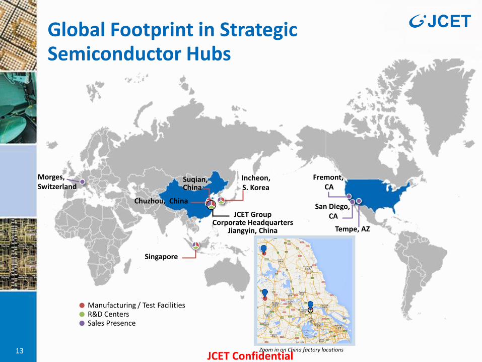
Global Footprint in Strategic Semiconductor Hubs
13
Incheon, S. Korea
JCET Group Corporate Headquarters
Jiangyin, China
Fremont, CA
Tempe, AZ
San Diego, CA
Morges, Switzerland
Singapore
Manufacturing / Test Facilities R&D Centers Sales Presence
Chuzhou, China
Suqian, China
Zoom in on China factory locations

JCET Confidential
Significant Manufacturing Scale
14
Plant R&D Only SCL
Plant JCET/JCAP
Low Power Discrete Factory Chuzhou, Anhui Province
120K m2 / 1,292K ft2 mfg
Leaded, discrete package and test
Campus 1: JCET HQ, JCAP B1 Middle Binjiang Road, Jiangyin
61K m2 / 661K ft2 mfg
Bumping, wafer level pkg & test
1
5
Power Package Factory Suqian, Jiangsu Province
50K m2 / 538K ft2 mfg
Power package and test
4
Qingpu (Shanghai), China
Incheon (IFEZ) South Korea
Singapore
Jiangyin, China
Suqian, Jiangsu, China
4 6
3
5
Chuzhou, Anhui, China
Singapore (SCS) Yishun
75K m2 / 808K ft2
Advanced wafer level packaging, laminate, QFN & test
China (SCC) Quingpu District, Shanghai
91K m2 / 983K ft2
Leaded, laminate, stacked die, flip chip & memory cards
Relocating to Jiangyin by Sep 2017 (JSCC)
South Korea (SCK2, SCK3, SCK4) Incheon (IFEZ)
SCK3/3+: 227K m² / 2,445K ft²
SCK2: 20K m² / 212K ft²
SCK4: 7.5K m² / 81K ft²
Flip chip, Laminate (CSP, stacked die), SiP, pre-stack, SLT & final test
7
3
Singapore (SCS-WD) Woodlands
4.75K m2 / 51K ft2
R&D Center
8
6
8 7
2
Campus 3: SiP, MISpak, JCAP B2, Xinshun, SJsemi and JSCC Changshan Road, Jiangyin
187K m2 / 2,010K ft2 mfg
SiP, MISpak, flip chip, leaded, laminate, bumping, WLCSP, test & MIS
2
1
√
√
√ √
JCET Confidential 15
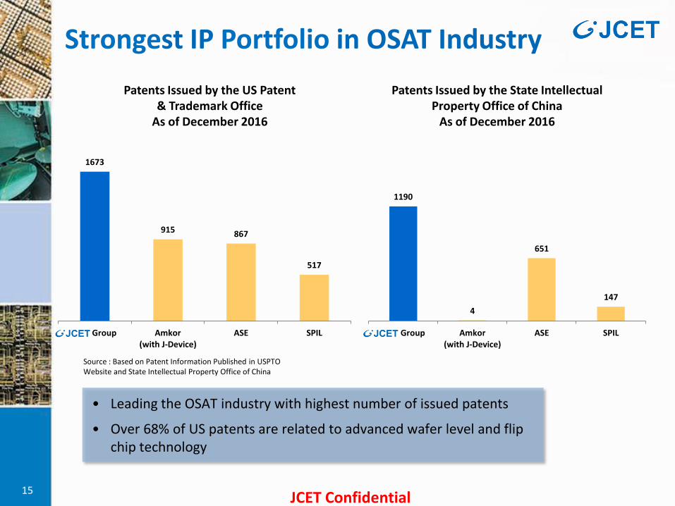
Source : Based on Patent Information Published in USPTO Website and State Intellectual Property Office of China
Patents Issued by the US Patent & Trademark Office
As of December 2016
Patents Issued by the State Intellectual Property Office of China
As of December 2016
1673
915 867
517
JCET Group Amkor (with J-Device)
ASE SPIL
1190
4
651
147
JCET Group Amkor (with J-Device)
ASE SPIL
Strongest IP Portfolio in OSAT Industry
• Leading the OSAT industry with highest number of issued patents
• Over 68% of US patents are related to advanced wafer level and flip chip technology

JCET Confidential
Patent Innovations Ranked among the Top 20 Semiconductor Equipment Manufacturing Companies Worldwide
• As a member of the JCET group of compannies, STATS ChipPAC has been ranked 8th in the Semiconductor Equipment Manufacturing scorecard, and the highest ranking among Outsourced Semiconductor Assembly and Test (OSAT)s in the 2016 published by the Institute of Electrical and Electronics Engineers (IEEE).
• This is the seventh consecutive year that the company has been recognized in the annual scorecards since 2010.

JCET Confidential
JCET Memory Package Trends
PoP FBGA LGA
L=1.4mm, T=1.2mm, V=1.0mm, W=0.8mm, U=0.65mm, X=0.50mm
FBGA-SD4(4D+3W) FBGA-SD5(5D+2W)
FBGA-PoPt-SD4(4D+1W)
Micro SD 4+1 SD SiP
FBGA-SD4(4D+0W)
FBGA-PoPt-SD4
FBGA-PoPt-SD3(3D+2W)
FBGA-PoPt-SD2(2D)
HVM
FBGA-SD6, eMMC
FBGA-SD8(8D+0W)
Development
WFBGA-PoPt-SD4
TFBGA-SD7, 30 um WT, 1.03mm PGK T
TFBGA-SD8, 35 um WT, 1.13mm PGK T
VFBGA-SiP-SD8
Dual Driver USB 8+1
TFBGA-SD8, 25 um WT, 1.13mm PGK T
VFBGA-SiP-SD8
VFBGA-MD6 VFBGA-MD7
VFBGA-SiP-SD9
22-pin Connector 9-pin Connector R LED
SD-SiP
XL/MC-eWLB
JCET Confidential
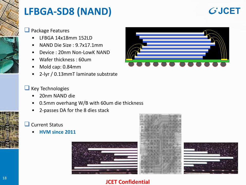
LFBGA-SD8 (NAND)
Package Features
• LFBGA 14x18mm 152LD
• NAND Die Size : 9.7x17.1mm
• Device : 20nm Non-LowK NAND
• Wafer thickness : 60um
• Mold cap: 0.84mm
• 2-lyr / 0.13mmT laminate substrate
Key Technologies
• 20nm NAND die
• 0.5mm overhang W/B with 60um die thickness
• 2-passes DA for the 8 dies stack
Current Status
• HVM since 2011
18

JCET Confidential
Package Features • VFBGA-SD6 11.5x13mm 153LD
• Nand flash Die Size: 10.33x8.12mm
• DDR Die Size: 6.32x2.69mm
• Controller Die Size: 6.79X1.82mm
• 0.13mm, 3-lyr coreless substrate
Key Technologies • 0.13T odd layer substrate handing
• SSB loop for die to die and die to substrate
• Warpage control w/ 3L substrate
Current Status
• HVM since 2012
Memory Stack Die – Mixed (FBGA-SD6) NAND + DDR + Controller

JCET Confidential
FLGA-SD9 (USB)
Package Features
• FLGA 11.1x16mm
• Memory Die Size : 8.2x11.1mm
• Controller Die Size: 2.9x2.4mm
• Device : 19nm Non-LowK + 65nm Lowk Controller
• Wafer thickness : 68um x 8 dies + 150um Controller
• 2-lyr / 0.21mmT laminate substrate
Key Technologies
• 19nm NAND die
• 8-Die Stack with Die-to-die bonding
• One-pass for the 8 NAND dies stack
Current Status
• HVM

JCET Confidential
Package Features
• FBGA 11.5x13mm 221LD e-MCP
• 4.115x1.385(Controller) : 60um
• 9.647x8.070(DRAM) : 75um
• 1.208x7.171(Nand) : 60um
• 9.00x8.00 (Film spacer) : 53um
• 2-lyr / 0.41mmT laminate substrate
Key Technologies
• 60um NAND flash die
• Film spacer application
• Dolmen and NAND cascade structure
Current Status
• HVM from ‘2016
Memory Stacked-Die – VFBGA-SD7
JCET Confidential
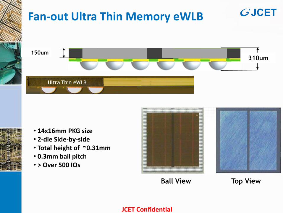
Fan-out Ultra Thin Memory eWLB
• 14x16mm PKG size • 2-die Side-by-side • Total height of ~0.31mm • 0.3mm ball pitch • > Over 500 IOs
Ball View Top View
150um 310um

Date
23
Innovations for Value

![Shadowofnoncommutativegeometry inspiredblackhole … · 2018. 9. 13. · arXiv:1501.06298v2 [gr-qc] 17 Aug 2015 Prepared for submissionto JCAP Shadowofnoncommutativegeometry inspiredblackhole](https://static.fdocuments.us/doc/165x107/5fefe2ff48056003df57d984/shadowofnoncommutativegeometry-inspiredblackhole-2018-9-13-arxiv150106298v2.jpg)