![MM PAPER-1 PCM MM Roll No. AA · 2019-04-05 · 1-AA ] [ 3 ] [ P.T.O. MM MM MM MM MM MM MM MM MM MM MM MM MM 002. Two children Ramesh (on path ARB) and Sohan (on path ASB), travel](https://static.fdocuments.us/doc/165x107/5ea35c4e77202f22f01a32c1/mm-paper-1-pcm-mm-roll-no-aa-2019-04-05-1-aa-3-pto-mm-mm-mm-mm-mm.jpg)
Packaging - Outlines and Dimensionsww1.microchip.com/downloads/en/PackagingSpec/00049AF.pdf ·...
126
© 2006 Microchip Technology Inc. DS00049AF Packaging Specification
Transcript of Packaging - Outlines and Dimensionsww1.microchip.com/downloads/en/PackagingSpec/00049AF.pdf ·...

© 2006 Microchip Technology Inc. DS00049AF
PackagingSpecification

Note the following details of the code protection feature on Microchip devices:
• Microchip products meet the specification contained in their particular Microchip Data Sheet.
• Microchip believes that its family of products is one of the most secure families of its kind on the market today, when used in the intended manner and under normal conditions.
• There are dishonest and possibly illegal methods used to breach the code protection feature. All of these methods, to our knowledge, require using the Microchip products in a manner outside the operating specifications contained in Microchip’s Data Sheets. Most likely, the person doing so is engaged in theft of intellectual property.
• Microchip is willing to work with the customer who is concerned about the integrity of their code.
• Neither Microchip nor any other semiconductor manufacturer can guarantee the security of their code. Code protection does not mean that we are guaranteeing the product as “unbreakable.”
Code protection is constantly evolving. We at Microchip are committed to continuously improving the code protection features of ourproducts. Attempts to break Microchip’s code protection feature may be a violation of the Digital Millennium Copyright Act. If such actsallow unauthorized access to your software or other copyrighted work, you may have a right to sue for relief under that Act.
Information contained in this publication regarding deviceapplications and the like is provided only for your convenienceand may be superseded by updates. It is your responsibility toensure that your application meets with your specifications.MICROCHIP MAKES NO REPRESENTATIONS OR WAR-RANTIES OF ANY KIND WHETHER EXPRESS OR IMPLIED,WRITTEN OR ORAL, STATUTORY OR OTHERWISE,RELATED TO THE INFORMATION, INCLUDING BUT NOTLIMITED TO ITS CONDITION, QUALITY, PERFORMANCE,MERCHANTABILITY OR FITNESS FOR PURPOSE.Microchip disclaims all liability arising from this information andits use. Use of Microchip’s products as critical components inlife support systems is not authorized except with expresswritten approval by Microchip. No licenses are conveyed,implicitly or otherwise, under any Microchip intellectual propertyrights.
DS00049AF-page ii Advance Info
Trademarks
The Microchip name and logo, the Microchip logo, Accuron, dsPIC, KEELOQ, microID, MPLAB, PIC, PICmicro, PICSTART, PRO MATE, PowerSmart, rfPIC, and SmartShunt are registered trademarks of Microchip Technology Incorporated in the U.S.A. and other countries.
AmpLab, FilterLab, Migratable Memory, MXDEV, MXLAB, PICMASTER, SEEVAL, SmartSensor and The Embedded Control Solutions Company are registered trademarks of Microchip Technology Incorporated in the U.S.A.
Analog-for-the-Digital Age, Application Maestro, dsPICDEM, dsPICDEM.net, dsPICworks, ECAN, ECONOMONITOR, FanSense, FlexROM, fuzzyLAB, In-Circuit Serial Programming, ICSP, ICEPIC, Linear Active Thermistor, MPASM, MPLIB, MPLINK, MPSIM, PICkit, PICDEM, PICDEM.net, PICLAB, PICtail, PowerCal, PowerInfo, PowerMate, PowerTool, Real ICE, rfLAB, rfPICDEM, Select Mode, Smart Serial, SmartTel, Total Endurance, UNI/O, WiperLock and Zena are trademarks of Microchip Technology Incorporated in the U.S.A. and other countries.
SQTP is a service mark of Microchip Technology Incorporated in the U.S.A.
All other trademarks mentioned herein are property of their respective companies.
© 2006, Microchip Technology Incorporated, Printed in the U.S.A., All Rights Reserved.
Printed on recycled paper.
rmation © 2006 Microchip Technology Inc.
Microchip received ISO/TS-16949:2002 quality system certification for its worldwide headquarters, design and wafer fabrication facilities in Chandler and Tempe, Arizona and Mountain View, California in October 2003. The Company’s quality system processes and procedures are for its PICmicro® 8-bit MCUs, KEELOQ® code hopping devices, Serial EEPROMs, microperipherals, nonvolatile memory and analog products. In addition, Microchip’s quality system for the design and manufacture of development systems is ISO 9001:2000 certified.

Packaging Index
CERAMIC SIDE-BRAZED DUAL IN-LINE FAMILY
8-Lead Ceramic Side-Brazed Dual In-line with Window (JW) – 300 mil Body ...................................... 314-Lead Ceramic Side-Brazed Dual In-line with Window (JW) – 300 mil Body .................................. 428-Lead Ceramic Side-Brazed Dual In-line with Window (JW) – 300 mil Body .................................... 5
CERAMIC DUAL IN-LINE (CERDIP) FAMILY
8-Lead Ceramic Dual In-line (JA) – 300 mil Body (CERDIP) ................................................................ 78-Lead Ceramic Dual In-line with Window (JW) – 300 mil Body (CERDIP) .......................................... 814-Lead Ceramic Dual In-line (JD) – 300 mil Body (CERDIP) .............................................................. 914-Lead Ceramic Dual In-line with Window (JW) – 300 mil Body (CERDIP) ...................................... 1016-Lead Ceramic Dual In-line (JE) – 300 mil Body (CERDIP) ............................................................ 1118-Lead Ceramic Dual In-line with Window (JW) – 300 mil Body (CERDIP) ...................................... 1220-Lead Ceramic Dual In-line with Window (JW) – 300 mil Body (CERDIP) ...................................... 1324-Lead Ceramic Dual In-line (JG) – 600 mil Body (CERDIP) ............................................................ 1428-Lead Ceramic Dual In-line (JJ) – 600 mil Body (CERDIP) ............................................................. 1528-Lead Ceramic Dual In-line with Window (JW) – 300 mil Body (CERDIP) ...................................... 1628-Lead Ceramic Dual In-line with Window (JW) – 600 mil Body (CERDIP) ...................................... 1740-Lead Ceramic Dual In-line (JK) – 600 mil Body (CERDIP) ............................................................ 1840-Lead Ceramic Dual In-line with Window (JW) – 600 mil Body (CERDIP) ...................................... 19
CERAMIC CHIP CARRIER (CERQUAD) FAMILY
68-Lead Ceramic Leaded (CL) Chip Carrier with Window – Square (CERQUAD) ............................. 2184-Lead Ceramic Leaded (CL) Chip Carrier with Window – Square (CERQUAD) ............................. 22
SMALL-OUTLINE TRANSISTOR FAMILY
3-Lead Plastic Transistor Outline (TO) (TO-92) .................................................................................. 233-Lead Plastic Small Outline Transistor Header (MB) (SOT-89)......................................................... 245-Lead Plastic Small Outline Transistor Header (MT) (SOT-89) ......................................................... 255-Lead Plastic Transistor Outline (AB) (TO-220)................................................................................. 265-Lead Thin Small Outline Transistor (OS) (TSOT) ............................................................................ 273-Lead Plastic Small Outline Transistor (TT) (SOT-23)....................................................................... 283-Lead Plastic Small Outline Transistor (TT) (SOT-23A) .................................................................... 293-Lead Plastic Small Outline Transistor (DB) (SOT-223) .................................................................... 304-Lead Plastic Small Outline Transistor (RC) (SOT-143).................................................................... 315-Lead Plastic Small Outline Transistor (OT) (SOT-23) ...................................................................... 326-Lead Plastic Small Outline Transistor (CH or OT) (SOT-23)............................................................ 333-Lead Plastic Small Outline Transistor (LB) (SC-70) ......................................................................... 345-Lead Plastic Small Outline Transistor (LT) (SC-70) ......................................................................... 35Leadless Wedge Module Plastic Small-Outline Transistor (WM) (SOT-385) ...................................... 36
DOUBLE DECA-WATT PACKAGE (DDPAK) FAMILY
3-Lead Plastic (EB) (DDPAK).............................................................................................................. 375-Lead Plastic (ET) (DDPAK) .............................................................................................................. 387-Lead Plastic (EK) (DDPAK).............................................................................................................. 39
© 2006 Microchip Technology Inc. DS00049AF-page iii

Packaging Index
PLASTIC DUAL IN-LINE (PDIP) FAMILY
8-Lead Plastic Dual In-line (P) – 300 mil Body (PDIP).........................................................................4114-Lead Plastic Dual In-line (P) – 300 mil Body (PDIP)....................................................................... 4216-Lead Plastic Dual In-line (P) – 300 mil Body (PDIP)....................................................................... 4318-Lead Plastic Dual In-line (P) – 300 mil Body (PDIP)....................................................................... 4420-Lead Plastic Dual In-line (P) – 300 mil Body (PDIP)....................................................................... 4524-Lead Plastic Dual In-line (P) – 600 mil Body (PDIP)....................................................................... 4624-Lead Skinny Plastic Dual In-line (SP) – 300 mil Body (PDIP) ........................................................ 4728-Lead Skinny Plastic Dual In-line (SP) – 300 mil Body (PDIP) ........................................................ 4828-Lead Plastic Dual In-line (P) – 600 mil Body (PDIP)....................................................................... 4940-Lead Plastic Dual In-line (P) – 600 mil Body (PDIP)....................................................................... 5064-Lead Shrink Plastic Dual In-line (SS) – 750 mil Body (PDIP) ......................................................... 51
PLASTIC LEADED CHIP CARRIER (PLCC) FAMILY
20-Lead Plastic Leaded Chip Carrier (L) – Square (PLCC)................................................................. 5328-Lead Plastic Leaded Chip Carrier (L) – Square (PLCC)................................................................. 5432-Lead Plastic Leaded Chip Carrier (L) – Rectangle (PLCC) ............................................................5544-Lead Plastic Leaded Chip Carrier (L) – Square (PLCC)................................................................. 5668-Lead Plastic Leaded Chip Carrier (L) – Square (PLCC)................................................................. 5784-Lead Plastic Leaded Chip Carrier (L) – Square (PLCC)................................................................. 58
PLASTIC SMALL-OUTLINE (SOIC/SOIJ) FAMILY
8-Lead Plastic Small-Outline (SN) – Narrow, 150 mil Body (SOIC)..................................................... 5914-Lead Plastic Small-Outline (SL) – Narrow, 150 mil Body (SOIC) ................................................... 6016-Lead Plastic Small-Outline (SL) – Narrow 150 mil Body (SOIC) ................................................... 618-Lead Plastic Small-Outline (SM) – Medium, 208 mil Body (SOIJ).................................................... 6216-Lead Plastic Small-Outline (SO) – Wide, 300 mil Body (SOIC)...................................................... 6318-Lead Plastic Small-Outline (SO) – Wide, 300 mil Body (SOIC)...................................................... 6420-Lead Plastic Small-Outline (SO) – Wide, 300 mil Body (SOIC)...................................................... 6524-Lead Plastic Small-Outline (SO) – Wide, 7.50 mm (.300 mil) Body (SOIC) ................................... 6628-Lead Plastic Small-Outline (SO) – Wide, 300 mil Body (SOIC)...................................................... 67
PLASTIC QUAD FLATPACK (QFN) AND PLASTIC DUAL FLATPACK (DFN) FAMILY
8-Lead Plastic Dual-Flat, No-Lead Package (MC) 2x3x0.9 mm Body (DFN) – Saw Singulated ......... 698-Lead Plastic Dual-Flat, No-Lead Package (MF) 6x5 mm Body (DFN-S) – Punch Singulated.......... 708-Lead Plastic Dual-Flat, No-Lead Package (MF) 3x3x0.9 mm Body (DFN) – Saw Singulated.......... 718-Lead Plastic Dual-Flat, No-Lead Package (MD) 4x4x0.9 mm Body (DFN-S) – Saw Singulated...... 728-Lead Plastic Dual-Flat, No-Lead Package (MF) 6x5 mm Body (DFN-S) – Saw Singulated............. 7310-Lead Plastic Dual-Flat, No-Lead Package (MF) 3x3x0.9 mm Body (DFN) – Saw Singulated........748-Lead Plastic Dual-Flat, No-Lead Package (ML) 4x4 mm Body (QFN) – Saw Singulated ................ 7516-Lead Plastic Quad-Flat No-Lead Package (ML) 4x4x0.9 mm Body (QFN) – Saw Singulated ....... 7620-Lead Plastic Quad-Flat No-Lead Package (ML) 4x4x0.9 mm Body, Saw Singulated (QFN) ......... 7728-Lead Plastic Quad-Flat No-Lead Package (ML) 6x6 mm Body (QFN) –
With 0.55 mm Contact Length (Saw Singulated) ..................................................................7828-Lead Plastic Quad-Flat No-Lead Package (ML) 6x6x0.9 mm Body (QFN-S) –
With 0.40 mm Contact Length (Saw Singulated) ..................................................................7944-Lead Plastic Quad-Flat No-Lead Package (ML) 8x8 mm Body (QFN) ........................................... 80
DS00049AF-page iv © 2006 Microchip Technology Inc.

Packaging Index
PLASTIC MICRO SMALL-OUTLINE (MSOP) FAMILY
8-Lead Plastic Micro Small-Outline Package (MS) (MSOP)................................................................ 8110-Lead Plastic Micro Small-Outline Package (MS) (MSOP).............................................................. 82
PLASTIC SHRINK SMALL-OUTLINE (SSOP) FAMILY
16-Lead Plastic Small-Outline Package Narrow Body (QR) (QSOP).................................................. 8320-Lead Plastic Shrink Small-Outline (SS) – 209 mil Body, 5.30 mm (SSOP)................................... 8424-Lead Plastic Shrink Small-Outline (SS) – (SSOP) ........................................................................ 8528-Lead Plastic Shrink Small-Outline (SS) – 209 mil Body, 5.30 mm (SSOP).................................... 86
PLASTIC THIN SHRINK SMALL-OUTLINE (TSSOP) FAMILY
8-Lead Plastic Thin Shrink Small-Outline (ST) – 4.4 mm Body (TSSOP) ........................................... 8714-Lead Plastic Thin Shrink Small-Outline (ST) – 4.4 mm Body (TSSOP) ......................................... 8820-Lead Plastic Thin Shrink Small-Outline (ST) – 4.4 mm Body (TSSOP) ......................................... 89
PLASTIC THIN SMALL-OUTLINE (TSOP) AND VERY SMALL OUTLINE (VSOP) FAMILY
28-Lead Plastic Thin Small-Outline (TS) – 5 x 20 mm Body (TSOP) .................................................. 9128-Lead Plastic Very Small Outline (VS) – 8 x 13.4 mm Body (VSOP) .............................................. 92
PLASTIC LOW-PROFILE QUAD FLATPACK (LQFP) FAMILY
32-Lead Plastic Low-Profile Quad Flatpack (PL) 7x7x1.4 mm Body,1.0/0.10 mm Lead Form (LQFP) ........................................................................................... 93
PLASTIC METRIC-QUAD FLATPACK (MQFP) FAMILY
44-Lead Plastic Metric-Quad Flatpack (PQ) 10x10x2 mm Body, 1.6/0.15 mm Lead Form (MQFP)... 9564-Lead Metric-Quad Flatpack (KU) 14x14x2.7 mm Body, 1.6/0.25 mm Lead Form (MQFP)............ 96
PLASTIC QUAD FLATPACK (PQFP) FAMILY
44-Lead Plastic Quad Flatpack (KW) 10x10x2.0 mm Body, 1.95/0.25 mm Lead Form (PQFP)......... 97
PLASTIC THIN-QUAD FLATPACK (TQFP) FAMILY
32-Lead Plastic Thin-Quad Flatpack (PT) 7x7x1 mm Body, 1.0/0.10 mm Lead Form (TQFP) ........... 9944-Lead Plastic Thin-Quad Flatpack (PT) 10x10x1 mm Body, 1.0/0.10 mm Lead Form (TQFP) ..... 10064-Lead Plastic Thin-Quad Flatpack (PT) 10x10x1 mm Body, 1.0/0.10 mm Lead Form (TQFP) ..... 10164-Lead Plastic Thin-Quad Flatpack (PT) 14x14x1 mm Body, 1.0/0.10 mm Lead Form (TQFP) ..... 10280-Lead Plastic Thin-Quad Flatpack (PT) 12x12x1 mm Body, 1.0/0.10 mm Lead Form (TQFP) ..... 10380-Lead Plastic Thin-Quad Flatpack (PT) 14x14x1 mm Body, 1.0/0.10 mm Lead Form (TQFP) ..... 104100-Lead Plastic Thin-Quad Flatpack (PT) 12x12x1 mm Body, 1.0/0.10 mm Lead Form (TQFP) ... 105100-Lead Plastic Thin-Quad Flatpack (PF) 14x14x1 mm Body, 1.0/0.10 mm Lead Form (TQFP) ... 106
© 2006 Microchip Technology Inc. DS00049AF-page v

Packaging Index
NOTES:
DS00049AF-page vi © 2006 Microchip Technology Inc.

PACKAGINGOutlines and Parameters
PART NUMBER SUFFIX DESIGNATIONS:XXXXXXXXXX – XX X/XX XXX
QTP, SQTP or ROM Code; Special Requirements
Package:1C = 1000 pF COB Module, .75 mm MF = Dual-Flat, No Leads (DFN-S)3C = 330 pF COB Module, .45 mm ML = Quad Flat No Leads (QFN)L = Plastic Leaded Chip Carrier (PLCC) MS = Plastic Micro Small Outline (MSOP)P = Plastic DIP MT = 5-Lead SOT-89 Small Outline TransistorS = Die in Waffle Pack OS = 5-Lead Thin Small Outline TransistorW = Die in Wafer Form OT = 5-Lead SOT-23 Small Outline TransistorAB = 5-lead TO-220 PF = 100-Lead Plastic Quad Flatpack (TQFP)CB = Chip on Board (COB) PQ = Plastic Metric-Quad Flatpack (MQFP)CH/OT = 6-Lead SOT-23 PL = Plastic Low-Profile Quad Flatpack (LQFP)CL = Windowed CERQUAD PT = Plastic Thin-Quad Flatpack (TQFP)DB/RC = Plastic Small Outline Transistor (SOT) QR = Plastic Small Outline Narrow Body (QSOP)EB = 3-lead DDPAK SB = Bumped Die in Waffle PackEK = 7-lead DDPAK SL = 14-lead Small Outline (150 mil)ET = 5-lead DDPAK SM = 8-lead Small Outline (207 mil)JA = 8-Lead Non-Windowed CERDIP SN = 8-lead Small Outline (150 mil)JD = 14-Lead Non-Windowed CERDIP SO = Plastic Small Outline (SOIC) (300 mil)JE = 16-Lead Non-Windowed CERDIP SP = Plastic Skinny DIPJG = 24-Lead Non-Windowed CERDIP SS = Plastic Shrink Small OutlineJJ = 28-Lead Non-Windowed CERDIP ST = Thin Shrink Small Outline (4.4 mm)JK = 40-Lead Non-Windowed CERDIP TO = Transistor OutlineJW = Windowed CERDIP TS = Thin Small Outline (8mm x 20 mm)KU = Metric-Quad Flatpack (MQFP) TT = 3-Lead SOT-23 Small Outline TransistorKW = Plastic Quad Flatpack (PQFP) VS = Very Small Outline (8 mm x 12 mm)LB = 3-Lead SC-70 WB = Bumped Wafer (11 mil)LT = 5-Lead SC-70 WF = Sawed Wafer on Frame (7 mil)MB = 3-Lead SOT-89 WFB = Bumped, Sawed Wafer on FrameMC = Dual-Flat, No Leads (DFN) WM = SOT-385 Leadless Module
Process Temperature:Blank = 0°C to +70°C E (Extended) = -40°C to +125°CI (Industrial) = -40°C to +85°C
Speed: OR Crystal Frequency Designator for PICmicro® MCUs-90 = 90 ns LP = DC to 20 MHz, High-Speed Crystal Oscillator-10 = 100 ns RC = DC to 2 MHz, XT and RC Oscillator Support-12 = 120 ns XT = DC to 4 MHz Internal, XT, RC Osc Support-15 = 150 ns HS = DC to 200 kHz, LP Oscillator Support-17 = 170 ns 02 = DC to 10 MHz, HS Oscillator Support-20 = 200 ns 04 = DC to 20 MHz, High-Speed Crystal Oscillator-25 = 250 ns 04 = DC to 2 MHz, XT and RC Oscillator Support-30 = 300 ns 10 = DC to 4 MHz Internal, XT, RC Osc Support
Option:T = Tape and Reel Shipments F = 200 μsBlank = twc = 1 ms X = Rotated pinout
Device Type: (Up to 10 digits)AA = 1.8V EEPROM Memory LCE = Low-Power CMOS/EPROM/EEPROM MCUC = CMOS EPROM MCU LCR = Low-Power CMOS ROM MCUCE = CMOS EPROM/EEPROM MCU LCS = Low-Power SecurityCR = CMOS ROM MCU LF = Low-Power Flash MCUF = Flash MCU LV = Low VoltageHC = High Speed 24 = 2-Wire (I2C™)HV = High Voltage 25 = SPI™
© 2006 Microchip Technology Inc. DS00049AF-page 1

Packaging
NOTES:
DS00049AF-page 2 © 2006 Microchip Technology Inc.

Packaging Diagrams and Parameters
8-Lead Ceramic Side-Brazed Dual In-line with Window (JW) – 300 mil Body
7.116.866.60.280.270.260ULid Width11.6811.4311.18.460.450.440TLid Length
4.344.224.09.171.166.161WWindow Diameter8.237.877.52.324.310.296eBOverall Row Spacing §0.510.460.41.020.018.016BLower Lead Width1.521.401.27.060.055.050B1Upper Lead Width0.300.250.20.012.010.008cLead Thickness3.813.563.30.150.140.130LTip to Seating Plane
13.4613.2112.95.530.520.510DOverall Length7.627.377.11.300.290.280E1Package Width1.140.890.64.045.035.025A1Standoff3.633.122.62.143.123.103A2Top of Body to Seating Plane4.704.193.68.185.165.145ATop to Seating Plane
2.54.100pPitch88nNumber of Pins
MAXNOMMINMAXNOMMINDimension LimitsMILLIMETERSINCHES*Units
2
1
D
n
T
E1
U
W
c
eB
L
A2
B
B1
A
A1
p
* Controlling Parameter§ Significant Characteristic
JEDEC Equivalent: MS-015Drawing No. C04-083
© 2006 Microchip Technology Inc. DS00049AF-page 3

Packaging Diagrams and Parameters
14-Lead Ceramic Side-Brazed Dual In-line with Window (JW) – 300 mil Body
7.116.866.60.280.270.260ULid Width11.6811.4311.18.460.450.440TLid Length4.344.224.09.171.166.161WWindow Diameter8.237.877.52.324.310.296eBOverall Row Spacing §0.510.460.41.020.018.016BLower Lead Width1.421.371.32.056.054.052B1Upper Lead Width0.300.250.20.012.010.008cLead Thickness3.813.563.30.150.140.130LTip to Seating Plane
17.9617.7817.60.707.700.693DOverall Length7.627.377.11.300.290.280E1Package Width1.140.890.64.045.035.025A1Standoff3.563.052.54.140.120.100A2Top of Body to Seating Plane4.624.113.61.182.162.142ATop to Seating Plane
2.54.100pPitch1414nNumber of Pins
MAXNOMMINMAXNOMMINDimension LimitsMILLIMETERSINCHES*Units
T
W
U
c
eB
2
1
D
n
E1
p
A2
L
A1
A
B1
B
* Controlling Parameter§ Significant CharacteristicJEDEC Equivalent: MS-015Drawing No. C04-107
DS00049AF-page 4 © 2006 Microchip Technology Inc.

Packaging Diagrams and Parameters
28-Lead Ceramic Side-Brazed Dual In-line with Window (JW) – 300 mil Body
7.497.246.99.295.285.275ULid Width12.9512.7012.45.510.500.490TLid Length
4.344.224.09.171.166.161WWindow Diameter8.237.877.52.324.310.296eBOverall Row Spacing §0.510.460.41.020.018.016BLower Lead Width1.321.271.22.052.050.048B1Upper Lead Width0.300.250.20.012.010.008cLead Thickness3.813.563.30.150.140.130LTip to Seating Plane
35.9235.5635.201.4141.4001.386DOverall Length7.627.377.11.300.290.280E1Package Width1.521.271.02.060.050.040A1Standoff3.943.432.92.155.135.115A2Top of Body to Seating Plane5.034.483.94.198.177.155ATop to Seating Plane
2.54.100pPitch2828nNumber of Pins
MAXNOMMINMAXNOMMINDimension LimitsMILLIMETERSINCHES*Units
c
eB
2
1
D
n
T
W
U
E1
p
A2
LA1
A
B1
B
* Controlling Parameter§ Significant CharacteristicJEDEC Equivalent: MS-015Drawing No. C04-084
© 2006 Microchip Technology Inc. DS00049AF-page 5

Packaging Diagrams and Parameters
NOTES:
DS00049AF-page 6 © 2006 Microchip Technology Inc.

Packaging Diagrams and Parameters
8-Lead Ceramic Dual In-line (JA) – 300 mil Body (CERDIP)
10.169.158.13.400.360.320eBOverall Row Spacing
0.510.460.41.020.018.016BLower Lead Width
1.651.401.14.065.055.045B1Upper Lead Width
0.380.290.20.015.012.008cLead Thickness
5.084.133.18.200.163.125LTip to Seating Plane
10.169.789.40.400.385.370DOverall Length
7.626.735.84.300.265.230E1Ceramic Pkg. Width
8.137.757.37.320.305.290EShoulder to Shoulder Width
1.020.770.51.040.030.020A1Standoff §
5.084.574.06.200.180.160ATop to Seating Plane
2.54.100pPitch
88nNumber of Pins
MAXNOMMINMAXNOMMINDimension Limits
MILLIMETERSINCHES *Units
JEDEC Equivalent: MS-030Drawing No. C04-010
* Controlling Parameter
1
2
n
E1
c
eB
E
p
L
A2
B
B1
A
A1
§ Significant Characteristic
D
© 2006 Microchip Technology Inc. DS00049AF-page 7

Packaging Diagrams and Parameters
8-Lead Ceramic Dual In-line with Window (JW) – 300 mil Body (CERDIP)
10.169.158.13.400.360.320eBOverall Row Spacing
0.510.460.41.020.018.016BLower Lead Width
1.651.401.14.065.055.045B1Upper Lead Width
0.380.290.20.015.012.008cLead Thickness
5.084.133.18.200.163.125LTip to Seating Plane
10.169.789.40.400.385.370DOverall Length
7.626.735.84.300.265.230E1Ceramic Pkg. Width
8.137.757.37.320.305.290EShoulder to Shoulder Width
1.020.770.51.040.030.020A1Standoff §
5.084.574.06.200.180.160ATop to Seating Plane
2.54.100pPitch
88nNumber of Pins
MAXNOMMINMAXNOMMINDimension Limits
MILLIMETERSINCHES *Units
JEDEC Equivalent: MS-030Drawing No. C04-027
* Controlling Parameter
Window Diameter W .267 .270 .273 6.866.78 6.93
1
2
D
n
E1
c
eB
E
p
L
A2
B
B1
A
A1
W
§ Significant Characteristic
DS00049AF-page 8 © 2006 Microchip Technology Inc.

Packaging Diagrams and Parameters
14-Lead Ceramic Dual In-line (JD) – 300 mil Body (CERDIP)
10.419.148.25.410.360.325eBOverall Row Spacing
0.530.460.38.021.018.015BLower Lead Width
1.651.401.14.065.055.045B1Upper Lead Width
0.360.300.20.014.012.008cLead Thickness
5.084.143.18.200.163.125LTip to Seating Plane
19.8119.3019.10.780.760.752DOverall Length
7.527.327.11.296.288.280E1Ceramic Pkg. Width
8.257.757.37.325.305.290EShoulder-to-Shoulder Width
1.020.760.38.040.030.015A1Standoff §
5.084.574.06.200.180.160ATop to Seating Plane
2.54.100pPitch
1818nNumber of Pins
MAXNOMMINMAXNOMMINDimension Limits
MILLIMETERSINCHES*Units
JEDEC Equivalent: MS-030Drawing No. C04-002
* Controlling Parameter
Revised 09-16-05
§ Significant Characterist ic
1
2
D
n
E1
c
eB
E
p
L
A2
B
B1
A
A1
© 2006 Microchip Technology Inc. DS00049AF-page 9

Packaging Diagrams and Parameters
14-Lead Ceramic Dual In-line with Window (JW) – 300 mil Body (CERDIP)
10.419.148.25.410.360.325eBOverall Row Spacing
0.530.460.38.021.018.015BLower Lead Width
1.651.401.14.065.055.045B1Upper Lead Width
0.360.300.20.014.012.008cLead Thickness
5.084.143.18.200.163.125LTip to Seating Plane
19.8119.3019.10.780.760.752DOverall Length
7.527.327.11.296.288.280E1Ceramic Pkg. Width
8.257.757.37.325.305.290EShoulder to Shoulder Width
1.020.760.38.040.030.015A1Standoff §
5.084.574.06.200.180.160ATop to Seating Plane
2.54.100pPitch
1414nNumber of Pins
MAXNOMMINMAXNOMMINDimension Limits
MILLIMETERSINCHES *Units
JEDEC Equivalent: MS-030 ACDrawing No. C04-099
* Controlling Parameter
Window Diameter W .170.125 3.18.210 4.32 5.33
1
2
D
n
E1
c
eB
E
p
L
A2
B
B1
A
A1
W
§ Significant Characteristic
DS00049AF-page 10 © 2006 Microchip Technology Inc.

Packaging Diagrams and Parameters
16-Lead Ceramic Dual In-line (JE) – 300 mil Body (CERDIP)
10.419.148.25.410.360.325eBOverall Row Spacing
0.530.460.38.021.018.015BLower Lead Width
1.651.401.14.065.055.045B1Upper Lead Width
0.360.300.20.014.012.008cLead Thickness
5.084.143.18.200.163.125LTip to Seating Plane
19.8119.3019.10.780.760.752DOverall Length
7.527.327.11.296.288.280E1Ceramic Pkg. Width
8.257.757.37.325.305.290EShoulder to Shoulder Width
1.020.760.38.040.030.015A1Standoff §
5.084.574.06.200.180.160ATop to Seating Plane
2.54.100pPitch
1818nNumber of Pins
MAXNOMMINMAXNOMMINDimension Limits
MILLIMETERSINCHES *Units
JEDEC Equivalent: MS-030Drawing No. C04-003
* Controlling Parameter
1
2
n
E1
c
eB
E
p
L
A2
B
B1
A
A1
§ Significant Characteristic
D
© 2006 Microchip Technology Inc. DS00049AF-page 11

Packaging Diagrams and Parameters
18-Lead Ceramic Dual In-line with Window (JW) – 300 mil Body (CERDIP)
3.30 3.56 3.815.335.084.83.210.200.190W2Window Length
.150.140.130W1Window Width10.809.788.76.425.385.345eBOverall Row Spacing §
0.530.470.41.021.019.016BLower Lead Width1.521.401.27.060.055.050B1Upper Lead Width0.300.250.20.012.010.008cLead Thickness3.813.493.18.150.138.125LTip to Seating Plane
23.3722.8622.35.920.900.880DOverall Length7.497.377.24.295.290.285E1Ceramic Pkg. Width8.267.947.62.325.313.300EShoulder to Shoulder Width0.760.570.38.030.023.015A1Standoff4.194.063.94.165.160.155A2Ceramic Package Height4.954.644.32.195.183.170ATop to Seating Plane
2.54.100pPitch1818nNumber of Pins
MAXNOMMINMAXNOMMINDimension LimitsMILLIMETERSINCHES*Units
1
2
D
n
W2
E1
W1
c
eB
E
p
L
A2
B
B1
A
A1
* Controlling Parameter§ Significant CharacteristicJEDEC Equivalent: MO-036Drawing No. C04-010
DS00049AF-page 12 © 2006 Microchip Technology Inc.

Packaging Diagrams and Parameters
20-Lead Ceramic Dual In-line with Window (JW) – 300 mil Body (CERDIP)
4.24 4.32 4.39.173.170.167WWindow Diameter
10.419.788.25.410.385.325eBOverall Row Spacing
0.580.480.38.023.019.015BLower Lead Width
1.521.401.27.060.055.050B1Upper Lead Width
0.300.250.20.012.010.008cLead Thickness
5.083.513.18.200.138.125LTip to Seating Plane
24.6424.1323.93.970.950.942DOverall Length
7.527.327.11.296.288.280E1Ceramic Pkg. Width
8.257.957.82.325.313.308EShoulder to Shoulder Width
0.760.580.38.030.023.015A1Standoff
4.454.063.56.175.160.140A2Ceramic Package Height
5.084.654.32.200.183.170ATop to Seating Plane
2.54.100pPitch
2020nNumber of Pins
MAXNOMMINMAXNOMMINDimension Limits
MILLIMETERSINCHES *Units
1
2
D
n
E1
c
eB
E
p
L
A2
B
B1
A
A1
JEDEC Equivalent: MS-030
Drawing No. C04-115
* Controlling Parameter
W
© 2006 Microchip Technology Inc. DS00049AF-page 13

Packaging Diagrams and Parameters
24-Lead Ceramic Dual In-line (JG) – 600 mil Body (CERDIP)
18.0316.7615.88.710.660.625eBOverall Row Spacing
0.580.460.38.023.018.015BLower Lead Width
1.651.401.14.065.055.045B1Upper Lead Width
0.360.300.20.014.012.008cLead Thickness
5.084.143.18.200.163.125LTip to Seating Plane
32.2631.7531.551.2701.2501.242DOverall Length
13.4113.2113.00.528.520.512E1Ceramic Pkg. Width
15.88--15.44.625--.608EShoulder to Shoulder Width
----0.38----.015A1Standoff §4.45--3.56.175--.140A2Ceramic Package Height
5.724.834.32.225.190.170ATop to Seating Plane
2.54.100pPitch
2824nNumber of Pins
MAXNOMMINMAXNOMMINDimension Limits
MILLIMETERSINCHES *Units
JEDEC Equivalent: MS-032Drawing No. C04-004
* Controlling Parameter§ Significant Characteristic
2
1
D
n
E1
c
E
eBp
A2
L
B1
BA1
A
DS00049AF-page 14 © 2006 Microchip Technology Inc.

Packaging Diagrams and Parameters
28-Lead Ceramic Dual In-line (JJ) – 600 mil Body (CERDIP)
18.0316.7615.88.710.660.625eBOverall Row Spacing
0.580.460.38.023.018.015BLower Lead Width
1.651.401.14.065.055.045B1Upper Lead Width
0.380.300.20.015.012.008cLead Thickness
5.084.143.18.200.163.125LTip to Seating Plane
37.3436.8336.631.4701.4501.442DOverall Length
13.4113.2113.00.528.520.512E1Ceramic Pkg. Width
15.88--15.44.625--.608EShoulder to Shoulder Width
----0.38----.015A1Standoff §4.45--3.56.175--.140A2Ceramic Package Height
5.724.834.32.225.190.170ATop to Seating Plane
2.54.100pPitch
2828nNumber of Pins
MAXNOMMINMAXNOMMINDimension Limits
MILLIMETERSINCHES *Units
JEDEC Equivalent: MS-032Drawing No. C04-006
* Controlling Parameter
§ Significant Characteristic
2
1
D
n
E1
c
E
eBp
A2
L
B1
BA1
A
© 2006 Microchip Technology Inc. DS00049AF-page 15

Packaging Diagrams and Parameters
28-Lead Ceramic Dual In-line with Window (JW) – 300 mil Body (CERDIP)
3.30 3.56 3.817.877.627.37.310.300.290W2Window Length
.150.140.130W1Window Width10.809.788.76.425.385.345eBOverall Row Spacing §
0.530.470.41.021.019.016BLower Lead Width1.651.461.27.065.058.050B1Upper Lead Width0.300.250.20.012.010.008cLead Thickness3.683.563.43.145.140.135LTip to Seating Plane
37.7237.0236.321.4851.4581.430DOverall Length7.497.377.24.295.290.285E1Ceramic Pkg. Width8.267.947.62.325.313.300EShoulder to Shoulder Width0.760.570.38.030.023.015A1Standoff4.194.063.94.165.160.155A2Ceramic Package Height4.954.644.32.195.183.170ATop to Seating Plane
2.54.100pPitch2828nNumber of Pins
MAXNOMMINMAXNOMMINDimension LimitsMILLIMETERSINCHES*Units
2
1
D
n
W2
W1
E1
E
eB p
A2
L
B1B
A1
A
* Controlling Parameter
c
§ Significant CharacteristicJEDEC Equivalent: MO-058Drawing No. C04-080
DS00049AF-page 16 © 2006 Microchip Technology Inc.

Packaging Diagrams and Parameters
28-Lead Ceramic Dual In-line with Window (JW) – 600 mil Body (CERDIP)
7.377.116.86.290.280.270WWindow Diameter18.0316.7615.49.710.660.610eBOverall Row Spacing §
0.580.510.41.023.020.016BLower Lead Width1.651.461.27.065.058.050B1Upper Lead Width0.300.250.20.012.010.008cLead Thickness3.813.493.18.150.138.125LTip to Seating Plane
37.8537.0836.321.4901.4601.430DOverall Length13.3613.2113.06.526.520.514E1Ceramic Pkg. Width15.8815.2415.11.625.600.595EShoulder to Shoulder Width
1.520.950.38.060.038.015A1Standoff4.194.063.94.165.160.155A2Ceramic Package Height5.725.334.95.225.210.195ATop to Seating Plane
2.54.100pPitch2828nNumber of Pins
MAXNOMMINMAXNOMMINDimension LimitsMILLIMETERSINCHES*Units
2
1
D
n
E1
W
c
E
eBp
A2
L
B1
BA1
A
* Controlling Parameter§ Significant CharacteristicJEDEC Equivalent: MO-103Drawing No. C04-013
© 2006 Microchip Technology Inc. DS00049AF-page 17

Packaging Diagrams and Parameters
40-Lead Ceramic Dual In-line (JK) – 600 mil Body (CERDIP)
21
D
n
c
eB
E
p
L
B1B
A2
E1
18.0316.7615.88.710.660.625eBOverall Row Spacing
0.580.460.38.023.018.015BLower Lead Width
1.651.401.14.065.055.045B1Upper Lead Width
0.360.300.20.014.012.008cLead Thickness
5.084.143.18.200.163.125LTip to Seating Plane
52.5852.0751.872.0702.0502.042DOverall Length
13.4113.2113.00.528.520.512E1Ceramic Pkg. Width
15.8815.3714.99.625.605.590EShoulder to Shoulder Width
1.521.020.51.060.040.020A1Standoff §4.57--3.56.180--.140A2Ceramic Package Height
5.724.834.32.225.190.170ATop to Seating Plane
2.54.100pPitch
4040nNumber of Pins
MAXNOMMINMAXNOMMINDimension Limits
MILLIMETERSINCHES *Units
JEDEC Equivalent: MS-103Drawing No. C04-008
* Controlling Parameter§ Significant Characteristic
DS00049AF-page 18 © 2006 Microchip Technology Inc.

Packaging Diagrams and Parameters
40-Lead Ceramic Dual In-line with Window (JW) – 600 mil Body (CERDIP)
9.148.898.64.360.350.340WWindow Diameter18.0316.7615.49.710.660.610eBOverall Row Spacing §
0.580.510.41.023.020.016BLower Lead Width1.401.331.27.055.053.050B1Upper Lead Width0.360.280.20.014.011.008cLead Thickness3.683.563.43.145.140.135LTip to Seating Plane
52.3252.0751.822.0602.0502.040DOverall Length13.3613.2113.06.526.520.514E1Ceramic Pkg. Width15.8815.2415.11.625.600.595EShoulder to Shoulder Width
1.521.140.76.060.045.030A1Standoff4.194.063.94.165.160.155A2Ceramic Package Height5.725.214.70.225.205.185ATop to Seating Plane
2.54.100pPitch4040nNumber of Pins
MAXNOMMINMAXNOMMINDimension LimitsMILLIMETERSINCHES*Units
21
D
n
c
eB
E
pB1
B
* Controlling Parameter§ Significant CharacteristicJEDEC Equivalent: MO-103Drawing No. C04-014
E1
W
A2 A
A1
© 2006 Microchip Technology Inc. DS00049AF-page 19

Packaging Diagrams and Parameters
NOTES:
DS00049AF-page 20 © 2006 Microchip Technology Inc.

Packaging Diagrams and Parameters
68-Lead Ceramic Leaded (CL) Chip Carrier with Window – Square (CERQUAD)
45°
A3
A
B1 B
D2E2
E
E1
#leads=n1
2n 1
A2
A1
D1 D
R CH1 x 45°
R .010 MIN.
C
R .020 MIN.
DETAIL
L1
E3 D3
DETAIL
p
9.919.659.40.390.380.370WWindow Diameter
0.530.480.43.021.019.017BLower Lead Width
0.810.740.66.032.029.026B1Upper Lead Width
0.250.180.15.010.007.006CLead Thickness
1717n1Pins each side
20.32 REF.800 REFD3Overall Lead Centers
20.32 REF.800 REFE3Overall Lead Centers
24.5124.1323.62.965.950.930D1Ceramic Package Length
24.5124.1323.62.965.950.930E1Ceramic Package Width
25.2725.1525.02.995.990.985DOverall Package Length
25.2725.1525.02.995.990.985EOverall Package Width
0.760.640.51.030.025.020RCorner Radius (Others)
1.271.020.76.050.040.030CH1Corner Chamfer (1)
1.020.890.76.040.035.030A3Side One Chamfer Dim.
3.052.542.29.120.100.090A1Lead Height
3.35 REF.132 REFA2Package Thickness
4.834.373.94.190.172.155AOverall Height
1.27.050pPitch
6868nNumber of Pins
MAXNOMMINMAXNOMMINDimension Limits
MILLIMETERSINCHES*Units
JEDEC Equivalent: MO-087 Revised 07-22-05
* Controlling Parameter
E2Footprint
Footprint D2
Lead Length L1
.880
.006
.880
.910
-
.910
.940
-
.940
-
23.11
23.1122.35
0.15
22.35 23.88
23.88
-
REF: Reference Dimension, usually without tolerance, for information purposes only.Notes:
See ASME Y14.5M
Drawing No. C04-097
W
© 2006 Microchip Technology Inc. DS00049AF-page 21

Packaging Diagrams and Parameters
84-Lead Ceramic Leaded (CL) Chip Carrier with Window – Square (CERQUAD)
45°A3
A
B1B
D2E2
EE1
#leads=n1
CH1 x 45°R 2n 1
A2 A1
D1 D
D3E3
L1
C
DETAIL
DETAIL
R .020 MIN.
R .010 MIN.p
.120
MAX
.190
.040 REF
.025
1.195
1.195
1.165
1.140
.010
.032.021
Units INCHES*Dimension Limits
Package Thickness
Side One Chamfer Dim.
Corner Radius (others)
Ceramic Package Width
Ceramic Package Length
Window Diameter
Lower Lead Width
Upper Lead Width
Number of Pins
Pitch
Overall Height
Lead Height
Corner Chamfer (1)
Overall Package Width
Overall Package Length
Footprint
Footprint
Lead Thickness
B1
.026 .029
.017
WB
.019
.395 .400
.155
.090
1.185
1.185
1.130
1.080
.006
CH1
R
E1
D1
E2
D2
C
E
D
A2
A1
A3
A
p
nMIN
1.190
1.190
1.150
1.110
1.110
.007
.100
.132 REF
.050
.172
.035
NOM
84
MILLIMETERS
0.66 0.74 0.81
0.43
.405 10.03 10.16
0.48
10.29
0.53
3.35 REF
NOM
4.37
30.23
30.23
29.21
29.31
28.19
0.18
30.10
30.10
28.70
27.43
0.15
MIN
3.94
2.29
1.02 REF
30.35
30.35
29.59
28.96
0.25
0.64
MAX
4.83
2.54
0.89
1.27
84
3.05
Pins each side n1 21 21
1.130 1.150 1.165
1.080 1.140
29.5928.70
28.9628.1927.43
.040.030 0.76 1.02
- - - -
Overall Lead Centers
Overall Lead Centers D3 1.00 REF 25.40 REF
E3 1.00 REF 25.40 REF
Lead Length L1 .006 - - 0.15 - -
REF: Reference Dimension, usually without tolerance, for information purposes only.
Revised 07-22-05JEDEC Equivalent: MO-087See ASME Y14.5M
* Controlling ParameterNotes:
Drawing No. C04-112
W
DS00049AF-page 22 © 2006 Microchip Technology Inc.

Packaging Diagrams and Parameters
3-Lead Plastic Transistor Outline (TO) (TO-92)
432432Mold Draft Angle Bottom654654
0.560.480.41.022.019.016BLead Width0.510.430.36.020.017.014cLead Thickness
2.412.292.16.095.090.085RMolded Package Radius4.954.644.32.195.183.170DOverall Length4.954.714.45.195.186.175E1Overall Width3.943.623.30.155.143.130ABottom to Package Flat
1.27.050pPitch33nNumber of Pins
MAXNOMMINMAXNOMMINDimension LimitsMILLIMETERSINCHES*Units
R
n1
3
p
L
B
A
c
1
D
2
E1
Tip to Seating Plane L .500 .555 .610 12.70 14.10 15.49
* Controlling Parameter
Mold Draft Angle Top
Notes:Dimensions D and E1 do not include mold flash or protrusions. Mold flash or protrusions shall not exceed .010” (0.254mm) per side.JEDEC Equivalent: TO-92Drawing No. C04-101
α
β
αβ
© 2006 Microchip Technology Inc. DS00049AF-page 23

Packaging Diagrams and Parameters
3-Lead Plastic Small Outline Transistor Header (MB) (SOT-89)
0.560.43.022.017BLead 2 Width
0.480.35.019.014cLead Thickness
1.831.62.072.064D1Tab Length
4.604.40.181.173DOverall Length
2.292.13.090.084E1Molded Package Width at Top
4.253.94.167.155HOverall Width
1.601.40.063.055AOverall Height
3.00 BSC.118 BSCp1Outside Lead Pitch
1.50 BSC.059 BSCpPitch
MAXMINMAXMINDimension Limits
MILLIMETERS*INCHESUnits
Dimensions D and E1 do not include mold flash or protrusions. Mold flash or protrusions shall not exceed .005" (0.127mm) per side.
Notes:
JEDEC Equivalent: TO-243
Revised 09-19-03
* Controlling Parameter
Foot Length L .035 .047 0.89 1.20
Leads 1 & 3 Width B1 .014 .019 0.36 0.48
Molded Package Width at Base E .090 .102 2.29 2.60
Tab Corner Radii R 0.254.010
BSC: Basic Dimension. Theoretically exact value shown without tolerances.
See ASME Y14.5M
p1
p
A
C
E
H
D D1
B1
L
E1
B1
B
1
2
3
R
Drawing No. C04-029
DS00049AF-page 24 © 2006 Microchip Technology Inc.
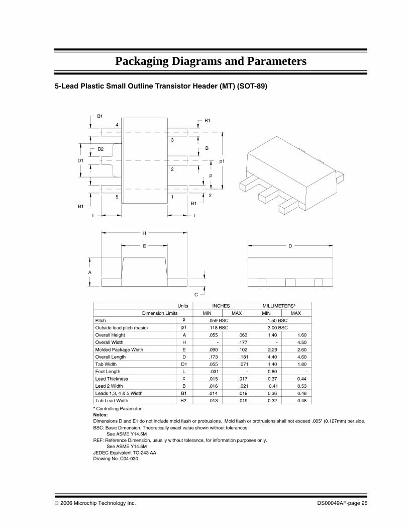
Packaging Diagrams and Parameters
5-Lead Plastic Small Outline Transistor Header (MT) (SOT-89)
0.530.41.021.016BLead 2 Width
0.440.37.017.015cLead Thickness
1.801.40.071.055D1Tab Width
4.604.40.181.173DOverall Length
4.50.177HOverall Width
1.601.40.063.055AOverall Height
3.00 BSC.118 BSCp1Outside lead pitch (basic)
1.50 BSC.059 BSCpPitch
MAXMINMAXMINDimension Limits
MILLIMETERS*INCHESUnits
Dimensions D and E1 do not include mold flash or protrusions. Mold flash or protrusions shall not exceed .005" (0.127mm) per side.Notes:* Controlling Parameter
Foot Length L .031 0.80
Leads 1,3, 4 & 5 Width B1 .014 .019 0.36 0.48
Molded Package Width E .090 .102 2.29 2.60
- -
--
Tab Lead Width B2 .013 .019 0.32 0.48
BSC: Basic Dimension. Theoretically exact value shown without tolerances.
REF: Reference Dimension, usually without tolerance, for information purposes only.See ASME Y14.5M
See ASME Y14.5M
JEDEC Equivalent TO-243 AA
D1
H
L
B1
B
B1
p
p1
E
C
A
1 2
2
3
L
B1
B1
4
5
B2
D
Drawing No. C04-030
© 2006 Microchip Technology Inc. DS00049AF-page 25

Packaging Diagrams and Parameters
5-Lead Plastic Transistor Outline (AB) (TO-220)
L H1
Q
E
β
e1
e
C1
J1
F
A
D
α (5°)
ØPEJECTOR PIN
e3
Drawing No. C04-036
Notes:Dimensions D and E1 do not include mold flash or protrusions. Mold flash or protrusions shall not exceed .010" (0.254 mm) per side.JEDEC equivalent: TO-220
* Controlling Parameter
Mold Draft Angle
Lead Width
Lead Thickness
α
C1
β
.014
Dimension Limits
Overall Height
Lead Length
Overall Width
Lead Pitch
A
L
E
.540
MIN
e
Units
.060
INCHES*
.022 0.36 0.56
MILLIMETERS
.190
.560 13.72
MINMAX
4.83
14.22
MAX
.160 4.06
3° 7° 3° 7°
Overall Length D
1.020.64.040.025
Overall Lead Centers e1 .263
.385
.560
.273 6.68 6.93
.072 1.52 1.83
.415 9.78 10.54
.590 14.22 14.99
Through Hole Diameter P .146 .156 3.71 3.96
J1Base to Bottom of Lead .090 2.29.115 2.92
Through Hole Center Q .103 2.87.113 2.62
Flag Thickness F .045 1.40.055 1.14
Flag Length H1 .234 6.55.258 5.94
Space Between Leads e3 .030 1.02.040 0.76
Revised 08-01-05
DS00049AF-page 26 © 2006 Microchip Technology Inc.

Packaging Diagrams and Parameters
5-Lead Thin Small Outline Transistor (OS) (TSOT)
1
p
DB
n
E
E1
L
c
β
φ
α
A2A
A1
p1
12°10°4°12°10°4°βMold Draft Angle Bottom
12°10°4°12°10°4°αMold Draft Angle Top
0.450.30.018.012BLead Width
0.200.150.09.008.006.004cLead Thickness
8°4°0°8°4°0°φFoot Angle
0.500.400.30.020.016.012LFoot Length
2.90.114DOverall Length
1.60.063E1Molded Package Width
3.002.802.60.118.110.102EOverall Width
0.100.050.01.004.002.000A1Standoff
0.900.870.84.035.034.033A2Molded Package Thickness
1.00.039AOverall Height
1.90 BSC..075 BSC.p1Outside lead pitch
0.95 BSC..037 BSC.pPitch
55nNumber of Pins
MAXNOMMINMAXNOMMINDimension Limits
MILLIMETERS*INCHESUnits
Dimensions D and E1 do not include mold flash or protrusions. Mold flash or protrusions shall not exceed .005" (0.127mm) per side.
Notes:
Drawing No. C04-128
* Controlling Parameter
BSC: Basic Dimension. Theoretically exact value shown without tolerances.
See ASME Y14.5MRevised 9-14-05
© 2006 Microchip Technology Inc. DS00049AF-page 27

Packaging Diagrams and Parameters
3-Lead Plastic Small Outline Transistor (TT) (SOT-23)
10°5°0°10°5°0°βMold Draft Angle Bottom
10°5°0°10°5°0°αMold Draft Angle Top
0.510.440.37.020.017.015BLead Width
0.180.140.09.007.006.004cLead Thickness
10°5°0°10°5°0°φFoot Angle
0.550.450.35.022.018.014LFoot Length
3.042.922.80.120.115.110DOverall Length
1.401.301.20.055.051.047E1Molded Package Width
2.642.372.10.104.093.083EOverall Width
0.100.060.01.004.002.000A1Standoff
1.020.950.88.040.037.035A2Molded Package Thickness
1.121.010.89.044.040.035AOverall Height
1.92.076p1Outside lead pitch (basic)
0.96.038pPitch
33nNumber of Pins
MAXNOMMINMAXNOMMINDimension Limits
MILLIMETERSINCHES*Units
.Dimensions D and E1 do not include mold flash or protrusions. Mold flash or protrusions shall not exceed .005" (0.127mm) per side
Notes:
JEDEC Equivalent: TO-236
* Controlling Parameter
BSC: Basic Dimension. Theoretically exact value shown without tolerances.
REF: Reference Dimension, usually without tolerance, for information purposes only.See ASME Y14.5M
See ASME Y14.5M
Drawing No. C04-104 Revised 07-19-05
2
1
p
DB
n
E
E1
L
c
βφ
α
A2A
A1
p1
DS00049AF-page 28 © 2006 Microchip Technology Inc.
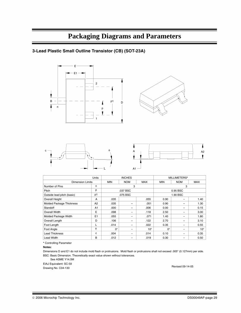
Packaging Diagrams and Parameters
3-Lead Plastic Small Outline Transistor (CB) (SOT-23A)
2
1
p
DB
n
E
E1
L
c φA2A
A1
p1
0.50–0.30.019–.012BLead Width
0.35–0.10.014–.004cLead Thickness
–φFoot Angle
0.55–0.35.022–.014LFoot Length
3.10–2.70.122–.106DOverall Length
1.80–1.40.071–.055E1Molded Package Width
3.00–2.50.118–.098EOverall Width
0.15–0.00.006–.000A1Standoff
1.30–0.90.051–.035A2Molded Package Thickness
1.40–0.90.055.035AOverall Height
1.90 BSC.075 BSCp1Outside lead pitch (basic)
0.95 BSC.037 BSCpPitch
33nNumber of Pins
MAXNOMMINMAXNOMMINDimension Limits
MILLIMETERS*INCHESUnits
Dimensions D and E1 do not include mold flash or protrusions. Mold flash or protrusions shall not exceed .005" (0.127mm) per side.
Notes:
EIAJ Equivalent: SC-59
* Controlling Parameter
10°0°10°–0°
Drawing No. C04-130 Revised 09-14-05
See ASME Y14.5MBSC: Basic Dimension. Theoretically exact value shown without tolerances.
© 2006 Microchip Technology Inc. DS00049AF-page 29

Packaging Diagrams and Parameters
3-Lead Plastic Small Outline Transistor (DB) (SOT-223)
0.850.65.033.026bLead Width
0.350.23.014.009cLead Thickness
6.706.30.264.248DOverall Length
7.30.287EOverall Width
1.80–.071–AOverall Height
4.60 BSC.181 BSCe1Outside lead pitch (basic)
2.30 BSC.091 BSCePitch
MAXMINMAXMINDimension Limits
MILLIMETERS*INCHESUnits
Dimensions D and E1 do not include mold flash or protrusions. Mold flash or protrusions shall not exceed .005" (0.127mm) per side.Notes:* Controlling Parameter
Molded Package Width E1 .130 .146 3.30 3.70
.264 6.70
Tab Lead Width b2 .114 .124 2.90 3.15
BSC: Basic Dimension. Theoretically exact value shown without tolerances. See ASME Y14.5M
JEDEC Equivalent TO-261 AA
Foot Length .035L 0.90– ––
.118
.030
.012
.256
.138
–
.276
3.00
–
0.30
0.76
–
3.50
6.50
7.00
NOM NOM
Lead Angle
Mold Draft Angle, Top
Mold Draft Angle, Bottom
φ
αβ
–
0.37
–
10°
0°
10° 10°16°–
10°
16°
–
–
–
10°
16°
10°
16°
Molded Package Height 1.651.55.063 .065A2 .061 1.60
Standoff –.001A1 .004– 0.02 0.10
Drawing No. C04-032 Revised 09-13-05
b2
D
E1 E
ee1
1
A
A1
A2
α
β
φ
Lb
c
DS00049AF-page 30 © 2006 Microchip Technology Inc.

Packaging Diagrams and Parameters
4-Lead Plastic Small Outline Transistor (RC) (SOT-143)
E
D
E1
A
A1
E2
(L1)
L
Φ c
b2 (3X) b
e1
e/2
e
1
4
2
3
§ Significant Characteristic
Drawing No. C04-031
Notes:Dimensions D and E1 do not include mold flash or protrusions. Mold flash or protrusions shall not exceed .010" (0.254mm) per side.
JEDEC equivalent: TO-253
* Controlling Parameter
.063 REF(L1)Footprint
Foot Angle
Leads 2, 3 & 4 Width
Lead Thickness c
b
Φ.003
0
–
–
Dimension Limits
Overall Height
Molded Package Thickness
Molded Package Width
Foot Length
Standoff §
Overall Width
Number of Pins
Pin 1 Offset
A
L
E1
A1
E
A2
.016 .020
.051
.002
.030
–
.035
MIN
e1
n
Units
.008 BSC
NOM
4
INCHES
1.60 REF
–
–
.008
8°
0.08
0
0.20
8°
MILLIMETERS*
0.20 BSC
0.90
1.30
0.50
–
.048
.024
.042
.006
0.40
0.05
0.75
MINMAX NOM
1.22
0.60
0.15
1.07
MAX
4
.031 – 0.80 –
– –
– –
Overall Length D .114 2.90
0.500.30.020.012
Pitch e .076 BSC 1.92 BSC
Lead 1 Width b1 .030 0.76– .035 – 0.89
.083
.047
.110
2.10
1.20
2.80
.104
.055
.120
2.64
1.40
3.04
Revised 08-12-05
© 2006 Microchip Technology Inc. DS00049AF-page 31

Packaging Diagrams and Parameters
5-Lead Plastic Small Outline Transistor (OT) (SOT-23)
1
p
DB
n
E
E1
L
c
β
φ
α
A2A
A1
p1
10501050bMold Draft Angle Bottom
10501050aMold Draft Angle Top
0.500.430.35.020.017.014BLead Width
0.200.150.09.008.006.004cLead Thickness
10501050fFoot Angle
0.550.450.35.022.018.014LFoot Length
3.102.952.80.122.116.110DOverall Length
1.751.631.50.069.064.059E1Molded Package Width
3.002.802.60.118.110.102EOverall Width
0.150.080.00.006.003.000A1Standoff
1.301.100.90.051.043.035A2Molded Package Thickness
1.451.180.90.057.046.035AOverall Height
1.90.075p1Outside lead pitch (basic)
0.95.038pPitch
55nNumber of Pins
MAXNOMMINMAXNOMMINDimension Limits
MILLIMETERSINCHES*Units
Dimensions D and E1 do not include mold flash or protrusions. Mold flash or protrusions shall not exceed .005" (0.127mm) per side.Notes:
EIAJ Equivalent: SC-74ADrawing No. C04-091
* Controlling Parameter
Revised 09-12-05
DS00049AF-page 32 © 2006 Microchip Technology Inc.

Packaging Diagrams and Parameters
6-Lead Plastic Small Outline Transistor (CH or OT) (SOT-23)
1
DB
n
E
E1
L
c
β
φ
α
A2A
A1
p1
10501050βMold Draft Angle Bottom
10501050αMold Draft Angle Top
0.500.430.35.020.017.014BLead Width
0.200.150.09.008.006.004cLead Thickness
10501050φFoot Angle
0.550.450.35.022.018.014LFoot Length
3.102.952.80.122.116.110DOverall Length
1.751.631.50.069.064.059E1Molded Package Width
3.002.802.60.118.110.102EOverall Width
0.150.080.00.006.003.000A1Standoff
1.301.100.90.051.043.035A2Molded Package Thickness
1.451.180.90.057.046.035AOverall Height
1.90 BSC.075 BSCp1Outside lead pitch
0.95 BSC.038 BSCpPitch
66nNumber of Pins
MAXNOMMINMAXNOMMINDimension Limits
MILLIMETERSINCHES*Units
Dimensions D and E1 do not include mold flash or protrusions. Mold flash or protrusions shall not exceed .005" (0.127mm) per side.Notes:
JEITA (formerly EIAJ) equivalent: SC-74A
* Controlling Parameter
Drawing No. C04-120
BSC: Basic Dimension. Theoretically exact value shown without tolerances. See ASME Y14.5M
Revised 09-12-05
© 2006 Microchip Technology Inc. DS00049AF-page 33

Packaging Diagrams and Parameters
3-Lead Plastic Small Outline Transistor (LB) (SC-70)
0.400.15.016.006bLead Width
0.250.08.010.003cLead Thickness
0.460.21.018.008LFoot Length
2.251.80.089.071DOverall Length
1.351.15.053.045E1Molded Package Width
2.401.80.094.071EOverall Width
.0100.00.0004.000A1Standoff
1.000.80.039.031A2Molded Package Thickness
1.100.80.043.031AOverall Height
1.30 BSCp1Outside lead pitch
0.65 BSCpPitch
33Number of Pins
MAXMINMAXMINDimension Limits
MILLIMETERS*INCHESUnits
Dimensions D and E1 do not include mold flash or protrusions. Mold flash or protrusions shall not exceed .005" (0.127mm) per side.Notes:
JEITA (EIAJ) Equivalent: SC70
Drawing No. C04-060
* Controlling Parameter
L
b
E1
E
p
c
p1 D
1
2
3
A A2
A1
.026 BSC
.051 BSC
Updated 10-07-05
BSC: Basic Dimension. Theoretically exact value shown without tolerances.See ASME Y14.5M
DS00049AF-page 34 © 2006 Microchip Technology Inc.

Packaging Diagrams and Parameters
5-Lead Plastic Small Outline Transistor (LT) (SC-70)
0.300.15.012.006BLead Width
0.180.10.007.004cLead Thickness
0.300.10.012.004LFoot Length
2.201.80.087.071DOverall Length
1.351.15.053.045E1Molded Package Width
2.401.80.094.071EOverall Width
0.100.00.004.000A1Standoff
1.000.80.039.031A2Molded Package Thickness
1.100.80.043.031AOverall Height
0.65 (BSC).026 (BSC)pPitch
55nNumber of Pins
MAXNOMMINMAXNOMMINDimension Limits
MILLIMETERS*INCHESUnits
Dimensions D and E1 do not include mold flash or protrusions. Mold flash or protrusions shall not exceed .005" (0.127mm) per side.
Notes:
JEITA (EIAJ) Standard: SC-70Revised 07-19-05
* Controlling Parameter
Top of Molded Pkg toQ1 .004 .016 0.10 0.40
Lead Shoulder
BSC: Basic Dimension. Theoretically exact value shown without tolerances.See ASME Y14.5M
L
E1
E
c
D
1
Bp
A2 A
Q1
n
A1
Drawing No. C04-061
© 2006 Microchip Technology Inc. DS00049AF-page 35

Packaging Diagrams and Parameters
Leadless Wedge Module Plastic Small Outline Transistor (WM) (SOT-385)
1.201.101.00CH2Chamfer Distance, Vertical
12.2012.1012.00.480.476.472DOverall Length6.206.106.002.44.240.236EOverall Width
3.053.002.90.120.118.114AOverall HeightMAXNOMMINMAXNOMMINDimension Limits
MILLIMETERS*INCHESUnits
D
E
F
J
A
Width at Tapered End J .173 .177 .181 4.40 4.50 4.60Length of Flat F .193 .197 .200 4.90 5.00 5.10
CH1 x 45°
Chamfer Distance, Horizontal CH1 .039 .043 .047 1.00 1.10 1.20
CH2 x 45 °
.047.043.039
Bottom of Package to Chamfer 2.102.001.90.083.079.075A1
A1
TYP.
TYP.
4 6 8864864Mold Draft Angle Top
Mold Draft Angle Bottom 4 6 8* Controlling ParameterNotes:Dimensions D, E, F and J do not include mold flash or protrusions. Mold flash or protrusions shall not exceed .010” (0.254mm) per side. Drawing No. C04-109
α
β
βα
DS00049AF-page 36 © 2006 Microchip Technology Inc.

Packaging Diagrams and Parameters
3-Lead Plastic (EB) (DDPAK)
BOTTOM VIEW
TOP VIEW
E
D
b
b1
E1
D2
A
A1
c2
c L
D1
e
α
φ
(5X)
L3
1
§ Significant Characteristic
Revised 07-19-05
Notes:
Mold Draft Angle
Dimensions D and E do not include mold flash or protrusions. Mold flash or protrusions shall not exceed .010" (0.254mm) per side.
α 7°
Pitch
Number of Pins
Overall Width
Standoff §
Molded Package Length
Exposed Pad Width
Overall Height
MAX
Units
Dimension Limits
A1
E1
D
E
e
A
.000
.256 REF
INCHES*
1.00 BSC
MIN
3
NOM MAX
.010 0.00
6.50 REF
MILLIMETERS
.183
MIN
3
2.54 BSC
NOM
0.25
4.65
JEDEC equivalent: TO-252
4.50.170
.005 0.13
Foot Length L .068 -- .110 1.73 -- 2.79
Foot Angle φ -- -- 8°
b1 .049 .050 .051 1.24 1.27 1.30
.177
* Controlling Parameter
4.32
.385 .398 .410 9.78 10.11 10.41
Overall Length D1
Upper Lead Width
Lead Thickness c .014 .020 .026 0.36 0.51 0.66
Pad Thickness c2 .045 -- .055 1.14 -- 1.40
Lower Lead Width .037b .026 .032 0.66 0.81 0.94
3° --
8°
7°3°
--
--
--
Exposed Pad Length D2 .303 REF 7.70 REF
Pad Length L3 .045 -- .067 1.701.14 --
.370.330 .350 9.408.38 8.89
.577.549 .605 15.3713.94 14.66
BSC: Basic Dimension. Theoretically, exact value shown without tolerances.
REF: Reference Dimension, usually without tolerance, for information purposes only.See ASME Y14.5M
See ASME Y14.5M
Drawing No. C04-011
© 2006 Microchip Technology Inc. DS00049AF-page 37

Packaging Diagrams and Parameters
5-Lead Plastic (ET) (DDPAK)
BOTTOM VIEWTOP VIEW
E
D
b
E1
D2
A
A1
c2
c L
D1
e
α
Φ
(5X)
e
L3
1
§ Significant Characteristic
Revised 07-19-05
Notes:
Mold Draft Angle
Dimensions D and E do not include mold flash or protrusions. Mold flash or protrusions shall not exceed .010" (0.254mm) per side.
α 7°
Pitch
Number of Pins
Overall Width
Standoff §
Molded Package Length
Exposed Pad Width
Overall Height
MAX
Units
Dimension Limits
A1
E1
D
E
e
A
.398
.000
.256 REF
INCHES*
.067 BSC
MIN
5
NOM MAX
.010 0.00
10.11
6.50 REF
MILLIMETERS
.183
MIN
5
1.70 BSC
NOM
0.25
4.65
JEDEC equivalent: TO-252
4.50.170
.005 0.13
Foot Length L .068 .089 .110 1.73 2.26 2.79
Foot Angle Φ -- -- 8°
.177
* Controlling Parameter
4.32
.385 .410 9.78 10.41
.330 .350 .370 8.38 8.89 9.40
Overall Length D1 .549 .577 .605 13.94 14.66 15.37
Lead Thickness c .014 .020 .026 0.36 0.51 0.66
Pad Thickness c2 .045 -- .055 1.14 -- 1.40
Lead Width .037b .026 .032 0.66 0.81 0.94
3° --
8°
7°3°
--
--
--
Exposed Pad Length D2 .303 REF 7.75 REF
Pad Length L3 .045 -- .067 1.14 -- 1.70
BSC: Basic Dimension. Theoretically exact value shown without tolerances.
REF: Reference Dimension, usually without tolerance, for information purposes only.See ASME Y14.5M
See ASME Y14.5M
Drawing No. C04-012
DS00049AF-page 38 © 2006 Microchip Technology Inc.

Packaging Diagrams and Parameters
7-Lead Plastic (EK) (DDPAK)
BOTTOM VIEW
TOP VIEW
E
D
b
E1
D2
A
A1
c2
c L
D1
α
Φ
(5X)
e
L3
1
§ Significant Characteristic
Notes:
Mold Draft Angle
Dimensions D and E do not include mold flash or protrusions. Mold flash or protrusions shall not exceed .010" (0.254mm) per side.
α 7°
Pitch
Number of Pins
Overall Width
Standoff §
Molded Package Length
Exposed Pad Width
Overall Height
MAX
Units
Dimension Limits
A1
E1
D
E
e
A
.398
.000
.256 REF
INCHES*
.050 BSC
MIN
5
NOM MAX
.010 0.00
10.11
6.50 REF
MILLIMETERS
.183
MIN
5
1.27 BSC
NOM
0.25
4.65
JEDEC equivalent: TO-252
4.50.170
.005 0.13
Foot Length L .068 .089 .110 1.73 2.26 2.79
Foot Angle Φ -- -- 8°
.177
* Controlling Parameter
4.32
.385 .410 9.78 10.41
.330 .350 .370 8.38 8.89 9.40
Overall Length D1 .549 .577 .605 13.94 14.66 15.37
Lead Thickness c .014 .020 .026 0.36 0.51 0.66
Pad Thickness c2 .045 -- .055 1.14 -- 1.40
Lead Width .037b .026 .032 0.66 0.81 0.94
3° --
8°
7°3°
--
--
--
Exposed Pad Length D2 .303 REF 7.75 REF
L3 .045 -- .067 1.701.14 --Pad Length
BSC: Basic Dimension. Theoretically exact value shown without tolerances.
REF: Reference Dimension, usually without tolerance, for information purposes only.See ASME Y14.5M
See ASME Y14.5M
Drawing No. C04-015
© 2006 Microchip Technology Inc. DS00049AF-page 39

Packaging Diagrams and Parameters
NOTES:
DS00049AF-page 40 © 2006 Microchip Technology Inc.

Packaging Diagrams and Parameters
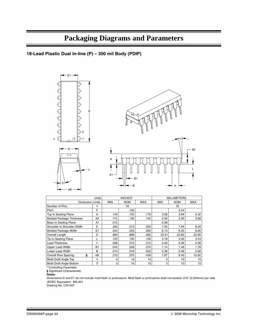
8-Lead Plastic Dual In-line (P) – 300 mil Body (PDIP)
B1
B
A1
A
L
A2
p
α
E
eB
β
c
E1
n
D
1
2
Units INCHES* MILLIMETERSDimension Limits MIN NOM MAX MIN NOM MAX
Number of Pins n 8 8Pitch p .100 2.54Top to Seating Plane A .140 .155 .170 3.56 3.94 4.32Molded Package Thickness A2 .115 .130 .145 2.92 3.30 3.68Base to Seating Plane A1 .015 0.38Shoulder to Shoulder Width E .300 .313 .325 7.62 7.94 8.26Molded Package Width E1 .240 .250 .260 6.10 6.35 6.60Overall Length D .360 .373 .385 9.14 9.46 9.78Tip to Seating Plane L .125 .130 .135 3.18 3.30 3.43Lead Thickness c .008 .012 .015 0.20 0.29 0.38Upper Lead Width B1 .045 .058 .070 1.14 1.46 1.78Lower Lead Width B .014 .018 .022 0.36 0.46 0.56Overall Row Spacing § eB .310 .370 .430 7.87 9.40 10.92Mold Draft Angle Top α 5 10 15 5 10 15Mold Draft Angle Bottom β 5 10 15 5 10 15* Controlling Parameter
Notes:Dimensions D and E1 do not include mold flash or protrusions. Mold flash or protrusions shall not exceed .010” (0.254mm) per side. JEDEC Equivalent: MS-001Drawing No. C04-018
§ Significant Characteristic
© 2006 Microchip Technology Inc. DS00049AF-page 41

Packaging Diagrams and Parameters
14-Lead Plastic Dual In-line (P) – 300 mil Body (PDIP)
E1
n
D
1
2
eB
β
E
c
A
A1
B
B1
L
A2
p
α
Units INCHES* MILLIMETERSDimension Limits MIN NOM MAX MIN NOM MAX
Number of Pins n 14 14Pitch p .100 2.54Top to Seating Plane A .140 .155 .170 3.56 3.94 4.32Molded Package Thickness A2 .115 .130 .145 2.92 3.30 3.68Base to Seating Plane A1 .015 0.38Shoulder to Shoulder Width E .300 .313 .325 7.62 7.94 8.26Molded Package Width E1 .240 .250 .260 6.10 6.35 6.60Overall Length D .740 .750 .760 18.80 19.05 19.30Tip to Seating Plane L .125 .130 .135 3.18 3.30 3.43Lead Thickness c .008 .012 .015 0.20 0.29 0.38Upper Lead Width B1 .045 .058 .070 1.14 1.46 1.78Lower Lead Width B .014 .018 .022 0.36 0.46 0.56Overall Row Spacing § eB .310 .370 .430 7.87 9.40 10.92Mold Draft Angle Top α 5 10 15 5 10 15
β 5 10 15 5 10 15Mold Draft Angle Bottom* Controlling Parameter
Notes:Dimensions D and E1 do not include mold flash or protrusions. Mold flash or protrusions shall not exceed .010” (0.254mm) per side. JEDEC Equivalent: MS-001Drawing No. C04-005
§ Significant Characteristic
DS00049AF-page 42 © 2006 Microchip Technology Inc.

Packaging Diagrams and Parameters
16-Lead Plastic Dual In-line (P) – 300 mil Body (PDIP)
2
1
D
n
E1
c
β
eB
E
α
p
L
A2
B
B1
A
A1
1510515105βMold Draft Angle Bottom
1510515105αMold Draft Angle Top
10.929.407.87.430.370.310eBOverall Row Spacing
0.560.46.036.022.018.014BLower Lead Width
1.781.461.14.070.058.045B1Upper Lead Width
0.380.290.20.015.012.008cLead Thickness
3.433.303.18.135.130.125LTip to Seating Plane
19.3019.0518.80.760.750.740DOverall Length
6.606.356.10.260.250.240E1Molded Package Width
8.267.947.62.325.313.300EShoulder to Shoulder Width
0.38.015A1Base to Seating Plane
3.683.302.92.145.130.115A2Molded Package Thickness
4.323.943.56.170.155.140ATop to Seating Plane
2.54.100pPitch
1616nNumber of Pins
MAXNOMMINMAXNOMMINDimension Limits
MILLIMETERSINCHES*Units
Dimensions D and E1 do not include mold flash or protrusions. Mold flash or protrusions shall not exceed .010" (0.254mm) per side.Notes:
JEDEC Equivalent: MS-001Revised 07-21-05
* Controlling Parameter
Drawing No. C04-017
© 2006 Microchip Technology Inc. DS00049AF-page 43
Packaging Diagrams and Parameters
18-Lead Plastic Dual In-line (P) – 300 mil Body (PDIP)
1510515105βMold Draft Angle Bottom1510515105αMold Draft Angle Top
10.929.407.87.430.370.310eBOverall Row Spacing §0.560.460.36.022.018.014BLower Lead Width1.781.461.14.070.058.045B1Upper Lead Width0.380.290.20.015.012.008cLead Thickness3.433.303.18.135.130.125LTip to Seating Plane
22.9922.8022.61.905.898.890DOverall Length6.606.356.10.260.250.240E1Molded Package Width8.267.947.62.325.313.300EShoulder to Shoulder Width
0.38.015A1Base to Seating Plane3.683.302.92.145.130.115A2Molded Package Thickness4.323.943.56.170.155.140ATop to Seating Plane
2.54.100pPitch1818nNumber of Pins
MAXNOMMINMAXNOMMINDimension LimitsMILLIMETERSINCHES*Units
1
2
D
n
E1
c
eB
β
E
α
p
A2
L
B1
B
A
A1
* Controlling Parameter
Notes:Dimensions D and E1 do not include mold flash or protrusions. Mold flash or protrusions shall not exceed .010” (0.254mm) per side. JEDEC Equivalent: MS-001Drawing No. C04-007
§ Significant Characteristic
DS00049AF-page 44 © 2006 Microchip Technology Inc.
Packaging Diagrams and Parameters
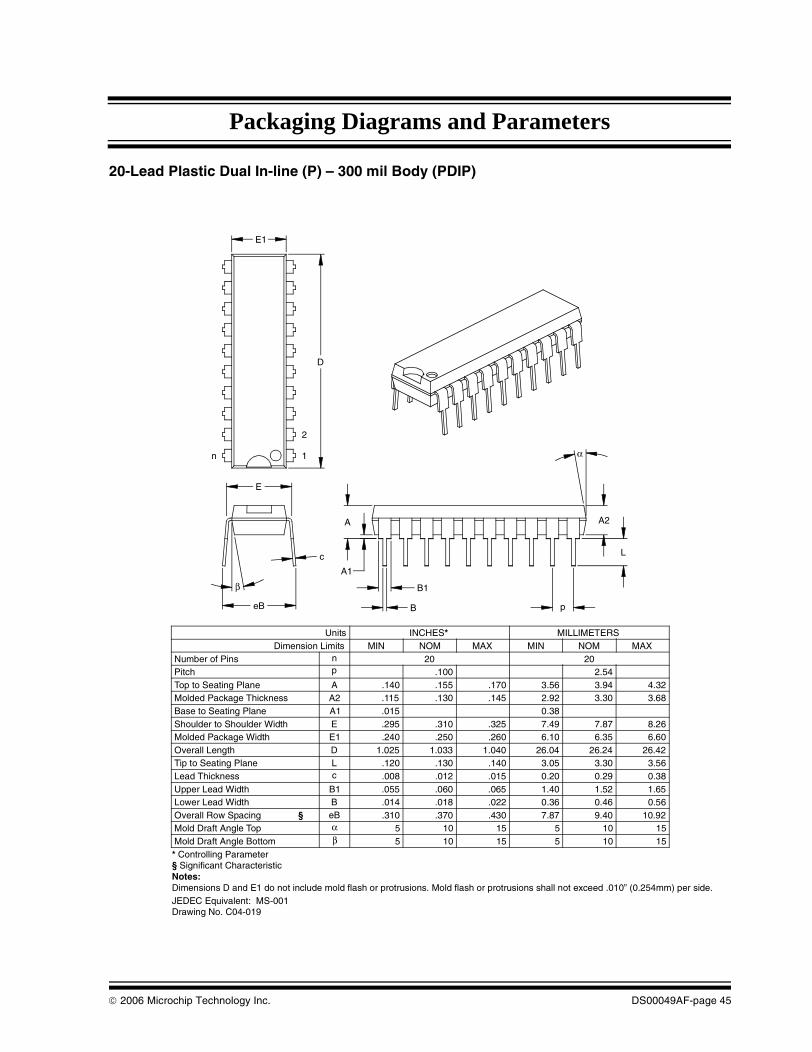
20-Lead Plastic Dual In-line (P) – 300 mil Body (PDIP)
1510515105βMold Draft Angle Bottom1510515105αMold Draft Angle Top
10.929.407.87.430.370.310eBOverall Row Spacing §0.560.460.36.022.018.014BLower Lead Width1.651.521.40.065.060.055B1Upper Lead Width0.380.290.20.015.012.008cLead Thickness3.563.303.05.140.130.120LTip to Seating Plane
26.4226.2426.041.0401.0331.025DOverall Length6.606.356.10.260.250.240E1Molded Package Width8.267.877.49.325.310.295EShoulder to Shoulder Width
0.38.015A1Base to Seating Plane3.683.302.92.145.130.115A2Molded Package Thickness4.323.943.56.170.155.140ATop to Seating Plane
2.54.100pPitch2020nNumber of Pins
MAXNOMMINMAXNOMMINDimension LimitsMILLIMETERSINCHES*Units
1
2
D
n
E1
c
β
eB
E
α
p
A2
L
B1
B
A
A1
* Controlling Parameter
Notes:Dimensions D and E1 do not include mold flash or protrusions. Mold flash or protrusions shall not exceed .010” (0.254mm) per side. JEDEC Equivalent: MS-001Drawing No. C04-019
§ Significant Characteristic
© 2006 Microchip Technology Inc. DS00049AF-page 45

Packaging Diagrams and Parameters
24-Lead Plastic Dual In-line (P) – 600 mil Body (PDIP)
1510515105βMold Draft Angle Bottom1510515105αMold Draft Angle Top
17.2716.5115.75.680.650.620eBOverall Row Spacing §0.560.460.36.022.018.014BLower Lead Width1.781.270.76.070.050.030B1Upper Lead Width0.380.290.20.015.012.008cLead Thickness3.433.303.05.135.130.120LTip to Seating Plane
31.8831.7531.621.2551.2501.245DOverall Length14.2213.8413.46.560.545.530E1Molded Package Width15.8815.2415.11.625.600.595EShoulder to Shoulder Width
0.38.015A1Base to Seating Plane4.063.813.56.160.150.140A2Molded Package Thickness4.834.454.06.190.175.160ATop to Seating Plane
2.54.100pPitch2424nNumber of Pins
MAXNOMMINMAXNOMMINDimension LimitsMILLIMETERSINCHES*Units
c
β
eB
E
2
1
D
n
E1
α
p
L
A2
B
A
A1B1
* Controlling Parameter
Notes:Dimensions D and E1 do not include mold flash or protrusions. Mold flash or protrusions shall not exceed .010” (0.254mm) per side. JEDEC Equivalent: MS-011Drawing No. C04-081
§ Significant Characteristic
DS00049AF-page 46 © 2006 Microchip Technology Inc.

Packaging Diagrams and Parameters
24-Lead Skinny Plastic Dual In-line (SP) – 300 mil Body (PDIP)
A2
2
1
D
n
E1
c
eB
E
β
α
p
L
B
B1
A
A1
1510515105βMold Draft Angle Bottom
1510515105αMold Draft Angle Top
10.929.407.87.430.370.310eBOverall Row Spacing
0.560.460.36.022.018.014BLower Lead Width
1.521.331.14.060.053.045B1Upper Lead Width
0.380.290.20.015.012.008cLead Thickness
3.303.183.05.130.125.120LTip to Seating Plane
31.8831.7531.621.2551.2501.245DOverall Length
6.606.356.10.260.250.240E1Molded Package Width
8.267.877.49.325.310.295EShoulder to Shoulder Width
0.38.015A1Base to Seating Plane
3.683.302.92.145.130.115A2Molded Package Thickness
4.063.813.56.160.150.140ATop to Seating Plane
2.54.100pPitch
2424nNumber of Pins
MAXNOMMINMAXNOMMINDimension Limits
MILLIMETERSINCHES*Units
Dimensions D and E1 do not include mold flash or protrusions. Mold flash or protrusions shall not exceed .010" (0.254mm) per side.Notes:
JEDEC Equivalent: MS-001 AFDrawing No. C04-043
* Controlling Parameter
Revised 09-14-05
© 2006 Microchip Technology Inc. DS00049AF-page 47

Packaging Diagrams and Parameters
28-Lead Skinny Plastic Dual In-line (SP) – 300 mil Body (PDIP)
1510515105βMold Draft Angle Bottom
1510515105αMold Draft Angle Top
10.928.898.13.430.350.320eBOverall Row Spacing §
0.560.480.41.022.019.016BLower Lead Width
1.651.331.02.065.053.040B1Upper Lead Width
0.380.290.20.015.012.008cLead Thickness
3.433.303.18.135.130.125LTip to Seating Plane
35.1834.6734.161.3851.3651.345DOverall Length
7.497.246.99.295.285.275E1Molded Package Width
8.267.877.62.325.310.300EShoulder to Shoulder Width
0.38.015A1Base to Seating Plane
3.433.303.18.135.130.125A2Molded Package Thickness
4.063.813.56.160.150.140ATop to Seating Plane
2.54.100pPitch
2828nNumber of Pins
MAXNOMMINMAXNOMMINDimension Limits
MILLIMETERSINCHES*Units
2
1
D
n
E1
c
eB
β
E
α
p
L
A2
B
B1
A
A1
Notes:
JEDEC Equivalent: MO-095Drawing No. C04-070
* Controlling Parameter
Dimension D and E1 do not include mold flash or protrusions. Mold flash or protrusions shall not exceed .010” (0.254mm) per side.
§ Significant Characteristic
DS00049AF-page 48 © 2006 Microchip Technology Inc.

Packaging Diagrams and Parameters
28-Lead Plastic Dual In-line (P) – 600 mil Body (PDIP)
1510515105βMold Draft Angle Bottom1510515105αMold Draft Angle Top
17.2716.5115.75.680.650.620eBOverall Row Spacing §0.560.460.36.022.018.014BLower Lead Width1.781.270.76.070.050.030B1Upper Lead Width0.380.290.20.015.012.008cLead Thickness3.433.303.05.135.130.120LTip to Seating Plane
37.2136.3235.431.4651.4301.395DOverall Length14.2213.8412.83.560.545.505E1Molded Package Width15.8815.2415.11.625.600.595EShoulder to Shoulder Width
0.38.015A1Base to Seating Plane4.063.813.56.160.150.140A2Molded Package Thickness4.834.454.06.190.175.160ATop to Seating Plane
2.54.100pPitch2828nNumber of Pins
MAXNOMMINMAXNOMMINDimension LimitsMILLIMETERSINCHES*Units
2
1
D
n
E1
c
β
eB
E
α
p
L
A2
BA1
A
B1
* Controlling Parameter
Notes:Dimensions D and E1 do not include mold flash or protrusions. Mold flash or protrusions shall not exceed .010” (0.254mm) per side. JEDEC Equivalent: MO-011Drawing No. C04-079
§ Significant Characteristic
© 2006 Microchip Technology Inc. DS00049AF-page 49

Packaging Diagrams and Parameters
40-Lead Plastic Dual In-line (P) – 600 mil Body (PDIP)
1510515105βMold Draft Angle Bottom1510515105αMold Draft Angle Top
17.2716.5115.75.680.650.620eBOverall Row Spacing §0.560.460.36.022.018.014BLower Lead Width1.781.270.76.070.050.030B1Upper Lead Width0.380.290.20.015.012.008cLead Thickness3.433.303.05.135.130.120LTip to Seating Plane
52.4552.2651.942.0652.0582.045DOverall Length14.2213.8413.46.560.545.530E1Molded Package Width15.8815.2415.11.625.600.595EShoulder to Shoulder Width
0.38.015A1Base to Seating Plane4.063.813.56.160.150.140A2Molded Package Thickness4.834.454.06.190.175.160ATop to Seating Plane
2.54.100pPitch4040nNumber of Pins
MAXNOMMINMAXNOMMINDimension LimitsMILLIMETERSINCHES*Units
A2
12
D
n
E1
c
βeB
E
α
p
L
B
B1
A
A1
* Controlling Parameter
Notes:Dimensions D and E1 do not include mold flash or protrusions. Mold flash or protrusions shall not exceed .010” (0.254mm) per side. JEDEC Equivalent: MO-011Drawing No. C04-016
§ Significant Characteristic
DS00049AF-page 50 © 2006 Microchip Technology Inc.
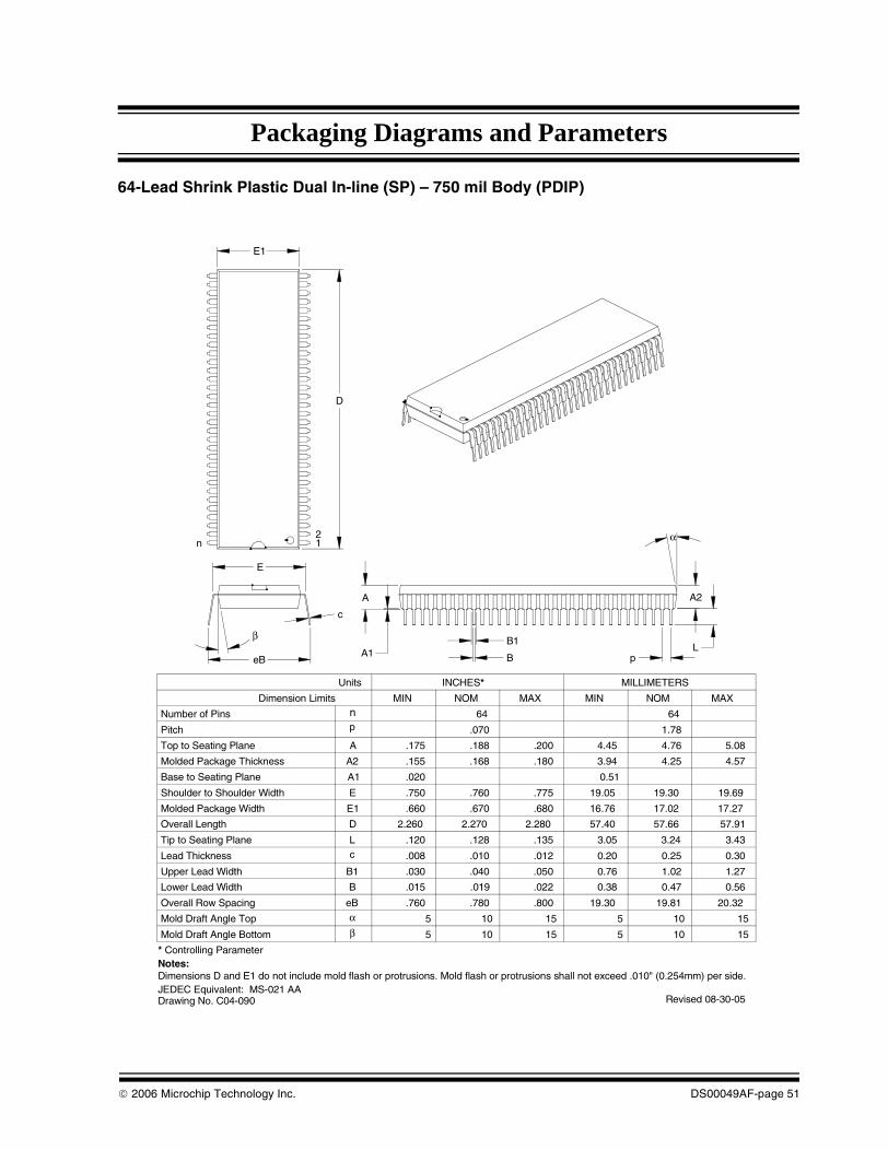
Packaging Diagrams and Parameters
64-Lead Shrink Plastic Dual In-line (SP) – 750 mil Body (PDIP)
A2
c
β
eB
E
12
D
n
E1
α
pL
B1
B
A
A1
1510515105βMold Draft Angle Bottom
1510515105αMold Draft Angle Top
20.3219.8119.30.800.780.760eBOverall Row Spacing
0.560.470.38.022.019.015BLower Lead Width
1.271.020.76.050.040.030B1Upper Lead Width
0.300.250.20.012.010.008cLead Thickness
3.433.243.05.135.128.120LTip to Seating Plane
57.9157.6657.402.2802.2702.260DOverall Length
17.2717.0216.76.680.670.660E1Molded Package Width
19.6919.3019.05.775.760.750EShoulder to Shoulder Width
0.51.020A1Base to Seating Plane
4.574.253.94.180.168.155A2Molded Package Thickness
5.084.764.45.200.188.175ATop to Seating Plane
1.78.070pPitch
6464nNumber of Pins
MAXNOMMINMAXNOMMINDimension Limits
MILLIMETERSINCHES*Units
Dimensions D and E1 do not include mold flash or protrusions. Mold flash or protrusions shall not exceed .010" (0.254mm) per side.Notes:
JEDEC Equivalent: MS-021 AARevised 08-30-05
* Controlling Parameter
Drawing No. C04-090
© 2006 Microchip Technology Inc. DS00049AF-page 51

Packaging Diagrams and Parameters
NOTES:
DS00049AF-page 52 © 2006 Microchip Technology Inc.

Packaging Diagrams and Parameters
20-Lead Plastic Leaded Chip Carrier (L) – Square (PLCC)
10501050βMold Draft Angle Bottom10501050αMold Draft Angle Top
0.530.510.33.021.020.013BLower Lead Width0.810.740.66.032.029.026B1Upper Lead Width0.330.270.20.013.011.008cLead Thickness
55n1Pins per Side
8.597.877.16.338.310.282D2Footprint Length8.597.877.16.338.310.282E2Footprint Width9.048.978.89.356.353.350D1Molded Package Length9.048.978.89.356.353.350E1Molded Package Width
10.039.919.78.395.390.385DOverall Length10.039.919.78.395.390.385EOverall Width
0.510.380.25.020.015.010CH2Corner Chamfer (others)1.271.141.02.050.045.040CH1Corner Chamfer 11.421.241.07.056.049.042A3Side 1 Chamfer Height
0.51.020A1Standoff §4.063.873.68.160.153.145A2Molded Package Thickness4.574.394.19.180.173.165AOverall Height
1.27.050pPitch2020nNumber of Pins
MAXNOMMINMAXNOMMINDimension LimitsMILLIMETERSINCHES*Units
β
A2
c E2
2
DD1
n
#leads=n1
E
E1
1
αA3
A
B1
35°
Bp
D2
CH1 x 45°
A1
.028 .035 0.71 0.89
CH2 x 45°
* Controlling Parameter
Notes:Dimensions D and E1 do not include mold flash or protrusions. Mold flash or protrusions shall not exceed .010” (0.254mm) per side. JEDEC Equivalent: MO-047Drawing No. C04-064
§ Significant Characteristic
© 2006 Microchip Technology Inc. DS00049AF-page 53

Packaging Diagrams and Parameters
28-Lead Plastic Leaded Chip Carrier (L) – Square (PLCC)
10501050βMold Draft Angle Bottom10501050αMold Draft Angle Top
0.530.510.33.021.020.013BLower Lead Width0.810.740.66.032.029.026B1Upper Lead Width0.330.270.20.013.011.008cLead Thickness
77n1Pins per Side
10.9210.6710.41.430.420.410D2Footprint Length10.9210.6710.41.430.420.410E2Footprint Width11.5811.5111.43.456.453.450D1Molded Package Length11.5811.5111.43.456.453.450E1Molded Package Width12.5712.4512.32.495.490.485DOverall Length12.5712.4512.32.495.490.485EOverall Width
0.250.130.00.010.005.000CH2Corner Chamfer (others)1.401.140.89.055.045.035CH1Corner Chamfer 10.790.660.53.031.026.021A3Side 1 Chamfer Height
0.51.020A1Standoff §4.063.873.68A2Molded Package Thickness4.574.394.19.180.173.165AOverall Height
1.27.050pPitch2828nNumber of Pins
MAXNOMMINMAXNOMMINDimension LimitsMILLIMETERSINCHES*Units
A2
c
E2
2
DD1
n
#leads=n1
E
E1
1
A3
A
B1
32°
B
p
D2
CH1 x 45°CH2 x 45 °
β
α
A1
.145 .153 .160.028 .035 0.71 0.89
* Controlling Parameter
Notes:Dimensions D and E1 do not include mold flash or protrusions. Mold flash or protrusions shall not exceed .010” (0.254mm) per side.
JEDEC Equivalent: MO-047Drawing No. C04-026
§ Significant Characteristic
DS00049AF-page 54 © 2006 Microchip Technology Inc.

Packaging Diagrams and Parameters
32-Lead Plastic Leaded Chip Carrier (L) – Rectangle (PLCC)
α
β
CH2 x 45° CH1 x 45°
10501050βMold Draft Angle Bottom10501050αMold Draft Angle Top
0.530.430.33.021.017.013BLower Lead Width0.810.740.66.032.029.026B1Upper Lead Width0.330.250.20.013.010.008cLead Thickness
99n2Pins along Length77n1Pins along Width
13.7212.9512.19.540.510.480D2Footprint Length11.1810.419.65.440.410.380E2Footprint Width14.0513.9713.89.553.550.547D1Molded Package Length11.5111.4311.35.453.450.447E1Molded Package Width15.1114.9914.86.595.590.585DOverall Length12.5712.4512.32.495.490.485EOverall Width
0.250.130.00.010.005.000CH2Corner Chamfer (others)1.401.140.89.055.045.035CH1Corner Chamfer 10.790.660.53.031.026.021A3Side 1 Chamfer Height
0.51.020A1Standoff §A2Molded Package Thickness
3.563.373.18.140.133.125AOverall Height
1.27.050pPitch3232nNumber of Pins
MAXNOMMINMAXNOMMINDimension LimitsMILLIMETERSINCHES*Units
A2
c
E2
2
DD1
n
#leads=n1
E
E1
1
A3
A1
A
B132°
B
p
D2
.105 .113 .120 2.67 2.87 3.05.028 .035 0.71 0.89
* Controlling Parameter
Notes:Dimensions D and E1 do not include mold flash or protrusions. Mold flash or protrusions shall not exceed .010” (0.254mm) per side. JEDEC Equivalent: MO-016Drawing No. C04-023
§ Significant Characteristic
© 2006 Microchip Technology Inc. DS00049AF-page 55
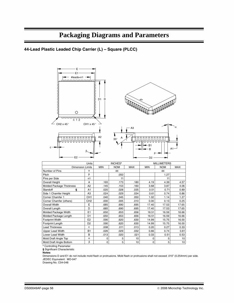
Packaging Diagrams and Parameters
44-Lead Plastic Leaded Chip Carrier (L) – Square (PLCC)
CH2 x 45° CH1 x 45°
10501050βMold Draft Angle Bottom10501050αMold Draft Angle Top
0.530.510.33.021.020.013B0.810.740.66.032.029.026B1Upper Lead Width0.330.270.20.013.011.008cLead Thickness
1111n1Pins per Side
16.0015.7514.99.630.620.590D2Footprint Length16.0015.7514.99.630.620.590E2Footprint Width16.6616.5916.51.656.653.650D1Molded Package Length16.6616.5916.51.656.653.650E1Molded Package Width17.6517.5317.40.695.690.685DOverall Length17.6517.5317.40.695.690.685EOverall Width
0.250.130.00.010.005.000CH2Corner Chamfer (others)1.271.141.02.050.045.040CH1Corner Chamfer 10.860.740.61.034.029.024A3Side 1 Chamfer Height
0.51.020A1Standoff §A2Molded Package Thickness
4.574.394.19.180.173.165AOverall Height
1.27.050pPitch4444nNumber of Pins
MAXNOMMINMAXNOMMINDimension LimitsMILLIMETERSINCHES*Units
β
A2
c
E2
2
DD1
n
#leads=n1
E
E1
1
α
p
A3
A35°
B1B
D2
A1
.145 .153 .160 3.68 3.87 4.06.028 .035 0.71 0.89
Lower Lead Width
* Controlling Parameter
Notes:Dimensions D and E1 do not include mold flash or protrusions. Mold flash or protrusions shall not exceed .010” (0.254mm) per side. JEDEC Equivalent: MO-047Drawing No. C04-048
§ Significant Characteristic
DS00049AF-page 56 © 2006 Microchip Technology Inc.

Packaging Diagrams and Parameters
68-Lead Plastic Leaded Chip Carrier (L) – Square (PLCC)
10501050βMold Draft Angle Bottom10501050αMold Draft Angle Top
0.530.510.33.021.020.013BLower Lead Width0.810.740.66.032.029.026B1Upper Lead Width0.330.270.20.013.011.008cLead Thickness
1717n1Pins per Side
23.6223.3722.61.930.920.890D2Footprint Length23.6223.3722.61.930.920.890E2Footprint Width24.3324.2324.13.958.954.950D1Molded Package Length24.3324.2324.13.958.954.950E1Molded Package Width25.2725.1525.02.995.990.985DOverall Length25.2725.1525.02.995.990.985EOverall Width
0.250.130.00.010.005.000CH2Corner Chamfer (others)1.271.141.02.050.045.040CH1Corner Chamfer 10.860.740.61.034.029.024A3Side 1 Chamfer Height
0.51.020A1Standoff §A2Molded Package Thickness
4.574.394.19.180.173.165AOverall Height
1.27.050pPitch68nNumber of Pins
MAXNOMMINMAXNOMMINDimension LimitsMILLIMETERSINCHES*Units
β
A2
c
E2
2
DD1
n
#leads=n1
E
E1
1α
pB
A3
A
B1
32°
D2
68
A1
.145 .153 .160 3.68 3.87 4.06.028 .035 0.71 0.89
CH1 x 45 °CH2 x 45°
* Controlling Parameter
Notes:Dimensions D and E1 do not include mold flash or protrusions. Mold flash or protrusions shall not exceed .010” (0.254mm) per side. JEDEC Equivalent: MO-047Drawing No. C04-049
§ Significant Characteristic
© 2006 Microchip Technology Inc. DS00049AF-page 57

Packaging Diagrams and Parameters
84-Lead Plastic Leaded Chip Carrier (L) – Square (PLCC)
10501050βMold Draft Angle Bottom10501050αMold Draft Angle Top
0.530.510.33.021.020.013BLower Lead Width0.810.740.66.032.029.026B1Upper Lead Width0.330.270.20.013.011.008cLead Thickness
1721n1Pins per Side
28.7028.1927.691.1301.1101.090D2Footprint Length28.7028.1927.691.1301.1101.090E2Footprint Width29.4129.3129.211.1581.1541.150D1Molded Package Length29.4129.3129.211.1581.1541.150E1Molded Package Width30.3530.2330.101.1951.1901.185DOverall Length30.3530.2330.101.1951.1901.185EOverall Width
0.510.380.25.020.015.010CH2Corner Chamfer (others)1.271.141.02.050.045.040CH1Corner Chamfer 11.271.141.02.050.045.040A3Side 1 Chamfer Height
0.51.020A1Standoff §A2Molded Package Thickness
4.574.394.19.180.173.165AOverall Height
1.27.050pPitch68nNumber of Pins
MAXNOMMINMAXNOMMINDimension LimitsMILLIMETERSINCHES*Units
β
A2
c
E2
2
DD1
n
#leads=n1
E
E1
1α
pB
A3
A
B1
45°
D2
84
A1
.145 .153 .160 3.68 3.87 4.06.028 .035 0.71 0.89
CH1 x 45 °CH2 x 45°
* Controlling Parameter
Notes:Dimensions D and E1 do not include mold flash or protrusions. Mold flash or protrusions shall not exceed .010” (0.254mm) per side. JEDEC Equivalent: MO-047Drawing No. C04-093
§ Significant Characteristic
DS00049AF-page 58 © 2006 Microchip Technology Inc.

Packaging Diagrams and Parameters
8-Lead Plastic Small Outline (SN) – Narrow, 150 mil Body (SOIC)
Foot Angle φ 0 4 8 0 4 8
1512015120βMold Draft Angle Bottom1512015120αMold Draft Angle Top
0.510.420.33.020.017.013BLead Width0.250.230.20.010.009.008cLead Thickness
0.760.620.48.030.025.019LFoot Length0.510.380.25.020.015.010hChamfer Distance5.004.904.80.197.193.189DOverall Length3.993.913.71.157.154.146E1Molded Package Width6.206.025.79.244.237.228EOverall Width0.250.180.10.010.007.004A1Standoff §1.551.421.32.061.056.052A2Molded Package Thickness1.751.551.35.069.061.053AOverall Height
1.27.050pPitch88nNumber of Pins
MAXNOMMINMAXNOMMINDimension LimitsMILLIMETERSINCHES*Units
2
1
D
n
p
B
E
E1
h
Lβ
c
45°
φ
A2
α
A
A1
* Controlling Parameter
Notes:Dimensions D and E1 do not include mold flash or protrusions. Mold flash or protrusions shall not exceed .010” (0.254mm) per side.
JEDEC Equivalent: MS-012Drawing No. C04-057
§ Significant Characteristic
© 2006 Microchip Technology Inc. DS00049AF-page 59

Packaging Diagrams and Parameters
14-Lead Plastic Small Outline (SL) – Narrow, 150 mil Body (SOIC)
Foot Angle φ 0 4 8 0 4 8
1512015120βMold Draft Angle Bottom1512015120αMold Draft Angle Top
0.510.420.36.020.017.014BLead Width0.250.230.20.010.009.008cLead Thickness
1.270.840.41.050.033.016LFoot Length0.510.380.25.020.015.010hChamfer Distance8.818.698.56.347.342.337DOverall Length3.993.903.81.157.154.150E1Molded Package Width6.205.995.79.244.236.228EOverall Width0.250.180.10.010.007.004A1Standoff §1.551.421.32.061.056.052A2Molded Package Thickness1.751.551.35.069.061.053AOverall Height
1.27.050pPitch1414nNumber of Pins
MAXNOMMINMAXNOMMINDimension LimitsMILLIMETERSINCHES*Units
2
1
D
p
nB
E
E1
h
L
c
β
45°
φ
α
A2A
A1
* Controlling Parameter
Notes:Dimensions D and E1 do not include mold flash or protrusions. Mold flash or protrusions shall not exceed .010” (0.254mm) per side. JEDEC Equivalent: MS-012Drawing No. C04-065
§ Significant Characteristic
DS00049AF-page 60 © 2006 Microchip Technology Inc.

Packaging Diagrams and Parameters
16-Lead Plastic Small Outline (SL) – Narrow 150 mil Body (SOIC)
Foot Angle φ 0 4 8 0 4 8
1512015120βMold Draft Angle Bottom1512015120αMold Draft Angle Top
0.510.420.33.020.017.013BLead Width0.250.230.20.010.009.008cLead Thickness
1.270.840.41.050.033.016LFoot Length0.510.380.25.020.015.010hChamfer Distance
10.019.919.80.394.390.386DOverall Length3.993.903.81.157.154.150E1Molded Package Width6.206.025.79.244.237.228EOverall Width0.250.180.10.010.007.004A1Standoff §1.551.441.32.061.057.052A2Molded Package Thickness1.751.551.35.069.061.053AOverall Height
1.27.050pPitch1616nNumber of Pins
MAXNOMMINMAXNOMMINDimension LimitsMILLIMETERSINCHES*Units
α
A2
E1
1
2
L
h
nB
45°
E
p
D
φ
β
c
A1
A
* Controlling Parameter
Notes:Dimensions D and E1 do not include mold flash or protrusions. Mold flash or protrusions shall not exceed .010” (0.254mm) per side. JEDEC Equivalent: MS-012Drawing No. C04-108
§ Significant Characteristic
© 2006 Microchip Technology Inc. DS00049AF-page 61

Packaging Diagrams and Parameters
8-Lead Plastic Small Outline (SM) – Medium, 208 mil Body (SOIJ)(JEITA/EIAJ Standard, Formerly called SOIC)
Foot Angle 0 4 8 0 4 8
1512015120Mold Draft Angle Bottom
1512015120Mold Draft Angle Top
0.510.430.36.020.017.014BLead Width
0.250.230.20.010.009.008cLead Thickness
0.760.640.51.030.025.020LFoot Length
5.335.215.13.210.205.202DOverall Length
5.385.285.11.212.208.201E1Molded Package Width
8.267.957.62.325.313.300EOverall Width
0.250.130.05.010.005.002A1Standoff
1.98.078A2Molded Package Thickness
2.03.080AOverall Height
1.27.050pPitch
88nNumber of Pins
MAXNOMMINMAXNOMMINDimension Limits
MILLIMETERSINCHES *Units
A2A
A1L
c
2
1
D
n
p
B
E
E1
.070 .075
.069 .074
1.78
1.75
1.97
1.88
Drawing No. C04-056
* Controlling ParameterNotes:Dimensions D and E1 do not include mold flash or protrusions. Mold flash or protrusions shall not exceed 0.10" (0.254mm) per side.
β
α
φ
βα
φ
DS00049AF-page 62 © 2006 Microchip Technology Inc.

Packaging Diagrams and Parameters
16-Lead Plastic Small Outline (SO) – Wide, 300 mil Body (SOIC)
Foot Angle φ 0 4 8 0 4 8
1512015120βMold Draft Angle Bottom1512015120αMold Draft Angle Top
0.510.420.36.020.017.014BLead Width0.330.280.23.013.011.009cLead Thickness
1.270.840.41.050.033.016LFoot Length0.740.500.25.029.020.010hChamfer Distance
10.4910.3010.10.413.406.398DOverall Length7.597.497.39.299.295.291E1Molded Package Width
10.6710.3410.01.420.407.394EOverall Width0.300.200.10.012.008.004A1Standoff §2.392.312.24.094.091.088A2Molded Package Thickness2.642.502.36.104.099.093AOverall Height
1.27.050pPitch1616nNumber of Pins
MAXNOMMINMAXNOMMINDimension LimitsMILLIMETERSINCHES*Units
Lβ
c
φ
h
45°
1
2
D
p
n
B
E1
E
α
A2
A1
A
* Controlling Parameter
Notes:Dimensions D and E1 do not include mold flash or protrusions. Mold flash or protrusions shall not exceed .010” (0.254mm) per side. JEDEC Equivalent: MS-013Drawing No. C04-102
§ Significant Characteristic
© 2006 Microchip Technology Inc. DS00049AF-page 63

Packaging Diagrams and Parameters
18-Lead Plastic Small Outline (SO) – Wide, 300 mil Body (SOIC)
Foot Angle φ 0 4 8 0 4 8
1512015120βMold Draft Angle Bottom1512015120αMold Draft Angle Top
0.510.420.36.020.017.014BLead Width0.300.270.23.012.011.009cLead Thickness
1.270.840.41.050.033.016LFoot Length0.740.500.25.029.020.010hChamfer Distance
11.7311.5311.33.462.454.446DOverall Length7.597.497.39.299.295.291E1Molded Package Width
10.6710.3410.01.420.407.394EOverall Width0.300.200.10.012.008.004A1Standoff §2.392.312.24.094.091.088A2Molded Package Thickness2.642.502.36.104.099.093AOverall Height
1.27.050pPitch1818nNumber of Pins
MAXNOMMINMAXNOMMINDimension LimitsMILLIMETERSINCHES*Units
Lβ
c
φ
h
45°
1
2
D
p
nB
E1
E
α
A2
A1
A
* Controlling Parameter
Notes:Dimensions D and E1 do not include mold flash or protrusions. Mold flash or protrusions shall not exceed 010” (0.254mm) per side. JEDEC Equivalent: MS-013Drawing No. C04-051
§ Significant Characteristic
DS00049AF-page 64 © 2006 Microchip Technology Inc.

Packaging Diagrams and Parameters
20-Lead Plastic Small Outline (SO) – Wide, 300 mil Body (SOIC)
* Controlling Parameter
Notes:Dimensions D and E1 do not include mold flash or protrusions. Mold flash or protrusions shall not exceed .010” (0.254mm) per side. JEDEC Equivalent: MS-013Drawing No. C04-094
Foot Angle φ 0 4 8 0 4 8
1512015120βMold Draft Angle Bottom1512015120αMold Draft Angle Top
0.510.420.36.020.017.014BLead Width0.330.280.23.013.011.009cLead Thickness
1.270.840.41.050.033.016LFoot Length0.740.500.25.029.020.010hChamfer Distance
13.0012.8012.60.512.504.496DOverall Length7.597.497.39.299.295.291E1Molded Package Width
10.6710.3410.01.420.407.394EOverall Width0.300.200.10.012.008.004A1Standoff §2.392.312.24.094.091.088A2Molded Package Thickness2.642.502.36.104.099.093AOverall Height
1.27.050pPitch2020nNumber of Pins
MAXNOMMINMAXNOMMINDimension LimitsMILLIMETERSINCHES*Units
h
L
c
β
45°
φ
1
2
D
p
nB
E
E1
α
A2A
A1
§ Significant Characteristic
© 2006 Microchip Technology Inc. DS00049AF-page 65

Packaging Diagrams and Parameters
24-Lead Plastic Small Outline (SO) – Wide, 7.50 mm (.300 mil) Body (SOIC)
2
1
D
e
n
B
E
E1
L
c
β
h
φA2
α
A
A1
h
Foot Angle φ 0° 8° 0° 8°
15°5°15°5°βMold Draft Angle Bottom
15°5°15°5°αMold Draft Angle Top
0.510.31.020.012BLead Width
0.330.20.013.008cLead Thickness
1.270.40.050.016LFoot Length
0.750.25.030.010hChamfer Distance
15.40 BSC.607 BSCDOverall Length
7.50 BSC.295 BSCE1Molded Package Width
10.30 BSC.406 BSCEOverall Width
0.300.10.012.004A1Standoff
2.552.05.100.081A2Molded Package Thickness
2.652.35.104.093AOverall Height
1.27 BSC.050 BSCePitch
2424nNumber of Pins
MAXNOMMINMAXNOMMINDimension Limits
MILLIMETERS*INCHESUnits
Dimensions D and E1 do not include mold flash or protrusions. Mold flash or protrusions shall not exceed .010" (0.254mm) per side.Notes:
JEDEC Equivalent: MS-013 ADRevised 07-19-05
* Controlling Parameter per JEDEC MS-103 Revision C.
-- --
-- --
-- --
-- --
-- --
-- --
-- --
-- --
-- --
-- --
BSC: Basic Dimension. Theoretically exact value shown without tolerances.See ASME Y14.5M
Drawing No. C04-025
DS00049AF-page 66 © 2006 Microchip Technology Inc.

Packaging Diagrams and Parameters
28-Lead Plastic Small Outline (SO) – Wide, 300 mil Body (SOIC)
Foot Angle Top φ 0 4 8 0 4 8
1512015120βMold Draft Angle Bottom1512015120αMold Draft Angle Top
0.510.420.36.020.017.014BLead Width0.330.280.23.013.011.009cLead Thickness
1.270.840.41.050.033.016LFoot Length0.740.500.25.029.020.010hChamfer Distance
18.0817.8717.65.712.704.695DOverall Length7.597.497.32.299.295.288E1Molded Package Width
10.6710.3410.01.420.407.394EOverall Width0.300.200.10.012.008.004A1Standoff §2.392.312.24.094.091.088A2Molded Package Thickness2.642.502.36.104.099.093AOverall Height
1.27.050pPitch2828nNumber of Pins
MAXNOMMINMAXNOMMINDimension LimitsMILLIMETERSINCHES*Units
21
D
p
n
B
E
E1
L
c
β
45°
h
φ
A2
α
A
A1
* Controlling Parameter
Notes:Dimensions D and E1 do not include mold flash or protrusions. Mold flash or protrusions shall not exceed .010” (0.254mm) per side. JEDEC Equivalent: MS-013Drawing No. C04-052
§ Significant Characteristic
© 2006 Microchip Technology Inc. DS00049AF-page 67

Packaging Diagrams and Parameters
NOTES:
DS00049AF-page 68 © 2006 Microchip Technology Inc.

Packaging Diagrams and Parameters
8-Lead Plastic Dual-Flat, No-Lead Package (MC) 2x3x0.9 mm Body (DFN) – Saw Singulated
L
E2
A3
A1A
TOP VIEW
D
E
EXPOSED
PADMETAL
D2
BOTTOM VIEW
2 1
b pn
(NOTE 3)
EXPOSEDTIE BAR
PIN 1
(NOTE 1)
ID INDEXAREA
(NOTE 2)
CONFIGURATIONCONTACT
ALTERNATEDETAIL
K
3. Package may have one or more exposed tie bars at ends.BSC: Basic Dimension. Theoretically exact value shown without tolerances.
REF: Reference Dimension, usually without tolerance, for information purposes only.
JEDEC Equivalent MO-229 VCED-2See ASME Y14.5M
See ASME Y14.5M
MILLIMETERS*
0.50 BSC
2.00 BSC
0.20 REF.
3.00 BSC
1. Pin 1 visual index feature may vary, but must be located within the hatched area.
.039.035.031 0.80AOverall Height
2. Exposed pad may vary according to die attach paddle size.
* Controlling Parameter
Contact Length §
Notes:
Contact Width
Standoff
Overall Width
Overall Length
Contact Thickness
Exposed Pad Width
Exposed Pad Length
.010.008
L
b .012 0.20
.001
.008 REF.
.079 BSC
–
–
.118 BSC
D
.051
.059
D2
E2
E
.000
A3
A1
.069
.075
1.30**
1.50**
.002 0.00
Dimension Limits
Pitch
Number of Pins
INCHES
.020 BSC
MINn
e
NOM
Units
8
MAX MIN
1.000.90
0.25 0.30
–
–
1.75
1.90
0.02 0.05
8
NOM MAX
Contact-to-Exposed Pad §
.012
K
.016 0.40.020 0.30 0.50
** Not within JEDEC parameters§ Significant Characteristic
.008 – – 0.20 ––
DWG No. C04-123
Revised 09-12-05
© 2006 Microchip Technology Inc. DS00049AF-page 69

Packaging Diagrams and Parameters
8-Lead Plastic Dual-Flat, No-Lead Package (MF) 6x5 mm Body (DFN-S) – Punch Singulated
NOM
.050 BSC
INCHES
.194 BSC
.184 BSC
.226 BSC
.236 BSC
.008 REF.
Dimensions D and E1 do not include mold flash or protrusions. Mold flash or protrusions shall not exceed .010" (0.254mm) per side.
DOverall Width
JEDEC equivalent: Pending
Notes:
JEDEC Equivalent MO-220
Molded Package Width
Lead Width
* Controlling Parameter
Mold Draft Angle Top
Tie Bar Width
Lead Length
Rα
B
L
D1
.014
.020
Dimension Limits
Molded Package Thickness
Pitch
Overall Height
Overall Length
Molded Package Length
Base Thickness
Standoff
Number of Pins
A3
E1
E
A2
A1
A
.000
Units
np
MIN
5.99 BSC
.019
12°
.030
.014
.016
.024
0.35
0.50
.356
0.40
0.60
5.74 BSC
12°
0.47
0.75
MILLIMETERS*
.039
.002
.031.026
.0004
.033
0.00
8
MAX MIN
1.27 BSC
0.20 REF.
4.92 BSC
4.67 BSC
0.85
0.01
0.65 0.80
0.05
1.00
MAXNOM
8
Exposed Pad Length E2
Exposed Pad Width D2 .085 .091 .097 2.16 2.31 2.46
.152 .158 .163 3.85 4.00 4.15
BSC: Basic Dimension. Theoretically exact value shown without tolerances.
REF: Reference Dimension, usually without tolerance, for information purposes only.See ASME Y14.5M
See ASME Y14.5M
Revised 07-19-05
TOP VIEW
1 2
A2
A
BOTTOM VIEW
n
E
E1
PIN 1
pB
EXPOSEDMETAL
PADS
D2
E2
A1A3
α
L
INDEX
D1 D
R
Drawing No. C04-113
DS00049AF-page 70 © 2006 Microchip Technology Inc.

Packaging Diagrams and Parameters
8-Lead Plastic Dual-Flat, No-Lead Package (MF) 3x3x0.9 mm Body (DFN) – Saw Singulated
D2
E
A1 A
A3
TOP VIEW
EXPOSEDMETAL
PAD
BOTTOM VIEW
2 1ID INDEX
PIN 1
D
L
E2
pbn
AREA(NOTE 1)
TIE BAR(NOTE 3)
EXPOSED
ALTERNATE EXPOSEDPAD CONFIGURATIONS
(NOTE 2)
K
2. Exposed pad varies according to die attach paddle size.
BSC: Basic Dimension. Theoretically exact value shown without tolerances.
REF: Reference Dimension, usually without tolerance, for information purposes only.
NOMINCHES
.026 BSC
.118 BSC.008 REF.
.118 BSC
3. Package may have one or more exposed tie bars at ends.
1. Pin 1 visual index feature may vary, but must be located within the hatched area.
JEDEC equivalent: M0-229
See ASME Y14.5M
See ASME Y14.5M
* Controlling Parameter
Revised 09-07-05
Exposed Pad Width
Number of Pins
Contact ThicknessOverall Length
Overall Height
Exposed Pad Length
Contact Length §Contact Width
Overall Width
Notes:
Standoff
Pitch
UnitsDimension Limits
D2
Lb
E2D
A1A3E
A
p
.043
.059
.008
.009
.000.031
MINn
MILLIMETERS*
.061
.092
.016
.012
.001
.035
.063
.096
.020
.015
.002
.039
8MAX
3.00 BSC0.20 REF.
0.65 BSC
3.00 BSC1.09
0.200.231.50
0.800.00
1.55
0.400.302.37
0.020.90
MIN NOM8
2.45
0.500.37
1.60
0.051.00
MAX
Contact-to-Exposed Pad § .008K – –– 0.20 –
§ Significant Characteristic
Drawing No. C04-062
© 2006 Microchip Technology Inc. DS00049AF-page 71

Packaging Diagrams and Parameters
8-Lead Plastic Dual-Flat, No-Lead Package (MD) 4x4x0.9 mm Body (DFN) – Saw Singulated
Exposed Pad Length
Exposed Pad Width
* Controlling Parameter
Contact Width
Drawing No. C04-131
Notes:
Overall Width
D2
E2
L
b
D
.016.008.009.127
.091
.012
Number of Pins
Standoff
Contact Thickness
Overall Length
Overall Height
Pitch pn
Units
A
A1
E
A3
Dimension Limits
8
.000 .001.008 REF.
.029.031 BSC
MININCHES
NOM
0.400.30
0.20.020
.144
.015
.112
0.233.23
2.30
0.500.383.65
2.85
0.020.75
0.20 REF.
0.80 BSC
MILLIMETERS*
.002
.0390.00
MINMAX NOM8
0.051.00
MAX
3. Exposed pad dimensions vary with paddle size.
1. Package may have one or more exposed tie bars at ends.2. Pin 1 visual index feature may vary, but must be located within the hatched area.
0.90.035
JEDEC equivalent: Not RegisteredRevised 9-14-05
.106
.138 3.50
2.70
BSC: Basic Dimension. Theoretically exact value shown without tolerances.See ASME Y14.5M
REF: Reference Dimension, usually without tolerance, for information purposes only.See ASME Y14.5M
.152 .157 .163 3.85 4.00 4.15
.152 .157 4.003.85.163 4.15(Note 3)
(Note 3)
K .008 – –0.20– –Contact Length §Contact-to-Exposed Pad §
§ Significant Characteristic
D2
E
A1 A
A3
TOP VIEW
EXPOSEDMETAL
PAD
BOTTOM VIEW
2 1
INDEX AREAPIN 1
D
L
E2
pb
n
(NOTE 1)
TIE BAR(NOTE 3)
EXPOSED
SIDE VIEW
(NOTE 2)
DS00049AF-page 72 © 2006 Microchip Technology Inc.

Packaging Diagrams and Parameters
8-Lead Plastic Dual-Flat, No-Lead Package (MF) 6x5 mm Body (DFN-S) – Saw Singulated
Notes:
JEDEC Equivalent: M0-220
Drawing No. C04-122
*
© 2006 Microchip Technology Inc. DS00049AF-page 73

Packaging Diagrams and Parameters
10-Lead Plastic Dual-Flat, No-Lead Package (MF) 3x3x0.9 mm Body (DFN)–Saw Singulated
E2
D
A1
A
A3
TOP VIEW
EXPOSEDMETAL
PAD
BOTTOM VIEW
2 1
ID INDEX
PIN 1
E
L
D2
pb
n
AREA
(NOTE 1)
TIE BAR
(NOTE 3)
EXPOSED
(NOTE 2)
K
BSC: Basic Dimension. Theoretically exact value shown without tolerances.
REF: Reference Dimension, usually without tolerance, for information purposes only.
INCHES
NOM
.020 BSC
.008 REF.
3. Package may have one or more exposed tie bars at ends.
1. Pin 1 visual index feature may vary, but must be located within the hatched area.
JEDEC equivalent: Not Registered
See ASME Y14.5M
See ASME Y14.5M
* Controlling Parameter
Revised 09-12-05
Standoff
Number of Pins
Overall Height
Contact Length §
Lead Width
Exposed Pad Width
Exposed Pad Length
Overall Width
Lead Thickness
Overall Length
Notes:
Pitch
Dimension Limits
(Note 3)
(Note 3)
L
D2
b
E
E2
D
A1
A3
.051
.012
.008
.000
.112
.082
.112
MIN
Units
e
A
n
.031
.065
.016
.010
.001
.118
.094
.118
.067
.020
.015
.002
.124
.096
.124
MAX
.035
10
.039
0.20 REF.
0.30
0.18
1.30
0.00
2.08
2.85
2.85
0.40
0.25
1.65
0.02
3.00
3.00
2.39
0.50 BSC
MILLIMETERS*
0.80
MIN
10
0.90
NOM
0.50
0.30
1.70
0.05
2.45
3.15
3.15
1.00
MAX
2. Exposed pad varies according to die attach paddle size.
Contact-to-Exposed Pad § K .008 — — 0.20 — —
§ Significant Characteristic
Drawing No. C04-063
DS00049AF-page 74 © 2006 Microchip Technology Inc.

Packaging Diagrams and Parameters
8-Lead Plastic Quad Flat No Lead Package (ML) 4x4 mm Body (QFN) – Saw Singulated
Exposed Pad Length
Exposed Pad Width
Contact Length
* Controlling Parameter
Contact Width
Drawing No. C04-300
Notes:
Package may have one or more exposed tie bars at ends.
Overall Width
D2
E2
L
b
D
.016.008
.009
.127
.091
.012
Number of Pins
Standoff
Contact Thickness
Overall Length
Overall Height
Pitch pn
Units
A
A1
E
A3
Dimension Limits
8
.000 .001
.008 REF.
.029
.031 BSC
MIN
INCHES
NOM
0.40
0.30
0.20.020
.144
.015
.112
0.23
3.23
2.30
0.50
0.38
3.65
2.85
0.02
0.75
0.20 REF.
0.80 BSC
MILLIMETERS*
.002
.039
0.00
MINMAX NOM
8
0.05
1.00
MAX
3.
1. Pin 1 visual index feature may vary, but must be located within the hatched area.Exposed pad dimensions vary with paddle size.2.
0.90.035
JEDEC equivalent: MO-229Revised 7-27-05
.106
.138 3.50
2.70
BSC: Basic Dimension. Theoretically exact value shown without tolerances.See ASME Y14.5M
REF: Reference Dimension, usually without tolerance, for information purposes only.See ASME Y14.5M
.152 .157 .163 3.85 4.00 4.15
.152 .157 4.003.85.163 4.15
D2
E
A1 A
A3
TOP VIEW
EXPOSEDMETAL
PAD
BOTTOM VIEW
2 1
INDEX AREAPIN 1
D
L
E2
pb
n
(NOTE 1)
TIE BAR(NOTE 3)
EXPOSEDSIDE VIEW
(NOTE 2)
© 2006 Microchip Technology Inc. DS00049AF-page 75

Packaging Diagrams and Parameters
16-Lead Plastic Quad Flat No Lead Package (ML) 4x4x0.9 mm Body (QFN) – Saw Singulated
2
1
n
D
E E2
D2
e
b
L
A A3
EXPOSEDMETAL
PAD
OPTIONALINDEXAREA
TOP VIEW BOTTOM VIEW
(NOTE 2)
(NOTE 1)
A1
K
BSC: Basic Dimension. Theoretically exact value shown without tolerances.
REF: Reference Dimension, usually without tolerance, for information purposes only.
JEDEC equivalent: M0-220 VGGC-3
See ASME Y14.5M
See ASME Y14.5M
* Controlling Parameter
Notes:
INCHES
NOM
.026 BSC
.008 REF
Number of Pins
Overall Height
Overall Width
Contact Width
Overall Length
Contact-to-Exposed Pad §
Exposed Pad Width
Exposed Pad Length
Contact Thickness
Pitch
Standoff
Units
Dimension Limits
e
E2
b
K
D2
D
A3
E
A1
A
.090**
.010
.008
.152
.090
.152
.000
.031
MINn
MIN
–
.157
.012
–
–
.035
.157
.001
.110
.014
.163
.110
–
.039
.163
.002
MAX
16
0.65 BSC
0.20 REF
2.29**
3.85
0.25
2.29
0.20
0.80
3.85
0.00
–
0.30
4.00
–
–
0.90
4.00
0.02
NOM
MILLIMETERS*
16
2.80
0.35
4.15
2.80
–
1.00
4.15
0.05
MAX
2. Exposed pad varies according to die attach paddle size.1. Pin 1 visual index feature may vary, but must be located within the hatched area.
§ Significant Characteristic
Contact Length § L .012 .016 0.30.020 0.40 0.50
** Outside JEDEC Specification
Drawing No. C04-127 Revised 09-13-05
DS00049AF-page 76 © 2006 Microchip Technology Inc.

Packaging Diagrams and Parameters
20-Lead Plastic Quad Flat No Lead Package (ML) 4x4x0.9 mm Body (QFN) – Saw Singulated
2
1
n
D
E E2
D2
e
b
L
A
A1
A3
EXPOSEDMETAL
PAD
OPTIONALINDEXAREA
TOP VIEW BOTTOM VIEW
(NOTE 1)
(NOTE 2)
2
1
K
INCHESNOM
.020 BSC
.008 REF
JEDEC equivalent: Not Registered
* Controlling Parameter
Number of Pins
Overall Height
Overall Width
Contact Width
Overall Length
Contact Length §
Exposed Pad Width
Exposed Pad Length
Contact Thickness
Notes:
Standoff
Pitch
UnitsDimension Limits
bL
D2D
A3
E2E
AA1
.007
.012
.102
.102
.000.031
MINne
MIN
.010
.016
.157 BSC.106
.106.157 BSC
.035.001
.012
.110
.020
.039
.110
.002
MAX20
0.20 REF
0.182.60
0.30
0.80
2.60
0.00
0.25
4.00 BSC2.70
0.40
0.90
4.00 BSC2.70
0.02
NOMMILLIMETERS*
0.50 BSC20
0.302.80
0.50
1.00
2.80
0.05
MAX
REF: Reference Dimension, usually without tolerance, for information purposes only.
BSC: Basic Dimension. Theoretically exact value shown without tolerances.
See ASME Y14.5M
See ASME Y14.5M
1. Pin 1 visual index feature may vary, but must be located within the hatched area.2. Exposed pad varies according to die attach paddle size.
.008Contact-to-Exposed Pad § K – – –0.20 –
§ Significant Characteristic
Drawing No. C04-126 Revised 09-12-05
© 2006 Microchip Technology Inc. DS00049AF-page 77

Packaging Diagrams and Parameters
28-Lead Plastic Quad Flat No Lead Package (ML) 6x6 mm Body (QFN) – With 0.55 mm Contact Length (Saw Singulated)
bD2D
PAD OUTLINEALTERNATE
SEE DETAIL
A1
A DETAIL
TOP VIEW
OPTIONALINDEXAREA
1
2
L
BOTTOM VIEW
n
E
METALPAD
ALTERNATE
EXPOSED
INDICATORSINDEX
e
E2
(NOTE 1)
(NOTE 2)
K
Contact Width
§ Significant Characteristic
Notes:
JEDEC equivalent: MO-220
β .009 .011 .013 0.23 0.28 0.33
Pitch
Number of Pins
Overall Width
Standoff
Overall Length
Overall Height
MAX
Units
Dimension Limits
A1
D
E
n
e
A
.000
INCHES
.026 BSC
MIN
28
NOM MAX
.002 0.00
6.00
MILLIMETERS*
.039
MIN
28
0.65 BSC
NOM
0.05
1.000.90.035
.001 0.02
Contact Length § L .018 .022 .024 0.45 0.55 0.65
E2
D2
Exposed Pad Width
Exposed Pad Length
.153 .167 .169 3.89 4.24 4.29
.031 0.80
5.90 6.10.240.236.232
.232 .236 6.00.240 5.90 6.10
.153 .167 4.24.169 3.89 4.29
Contact Thickness A3 .008 REF 0.20 REF
REF: Reference Dimension, usually without tolerance, for information purposes only.
BSC: Basic Dimension. Theoretically exact value shown without tolerances.
See ASME Y14.5M
See ASME Y14.5M
1. Pin 1 visual index feature may vary, but must be located within the hatched area.2. Exposed pad varies according to die attach paddle size.
Contact-to-Exposed Pad § K .008 – –0.20– –
* Controlling Parameter
Revised 09-12-05Drawing No. C04-105
DS00049AF-page 78 © 2006 Microchip Technology Inc.

Packaging Diagrams and Parameters
28-Lead Plastic Quad Flat No Lead Package (MM) 6x6x0.9 mm Body (QFN-S) – With 0.40 mm Contact Length (Saw Singulated)
E2E
D D2
2
1
2
1
e
b
K
n
L
EXPOSEDMETAL
PAD(NOTE 2)
OPTIONALINDEXAREA(NOTE 1)
ALTERNATE INDEX
INDICATORS
SEE DETAIL
BOTTOM VIEWTOP VIEW
A
A1DETAIL
ALTERNATEPAD OUTLINE
INCHES
NOM
.026 BSC
Number of Pins
Overall Width
Overall Length
Overall Height
Contact Length §
Exposed Pad Width
Exposed Pad Length
* Controlling Parameter
Lead Width
Notes:
Standoff
Pitch
D2 .144
.232
.013
.012
b
L
D
Units
Dimension Limits
A1
E2
MIN
.000
.144
.232E
A
e
n
.031
.015
.016
.236
.146
.240
.148
.017
.020
3.65
5.90
0.33
0.30
0.38
0.40
6.00
3.70
MAX
.001
.146
.236
.035
28
.002
.039
.148
.240
MILLIMETERS*
0.65 BSC
3.65
0.00
0.80
5.90
MIN
6.00
0.90
0.02
3.70
NOM
28
3.75
6.10
0.43
0.50
1.00
0.05
3.75
6.10
MAX
BSC: Basic Dimension. Theoretically exact value shown without tolerances.See ASME Y14.5M
1. Pin 1 visual index feature may vary, but must be located within the hatched area.2. Exposed pad varies according to die attach paddle size.
.008Contact-to-Exposed Pad § K –– – 0.20 –
§ Significant Characteristic
Drawing No. C04-124
Revised 1-12-06
© 2006 Microchip Technology Inc. DS00049AF-page 79

Packaging Diagrams and Parameters
44-Lead Plastic Quad Flat No Lead Package (ML) 8x8 mm Body (QFN)
D2D
TOP VIEW
n
1
LE2
BOTTOM VIEW
B
E
2
PIN 1INDEX ON
EXPOSED PAD
(NOTE 1)INDEX AREA
OPTIONAL
DETAIL: CONTACT VARIANTS
(PROFILE MAY VARY)
p
A1
A
A3
EXPOSEDMETAL PAD
(NOTE 2)
K
INCHES
NOM
.026 BSC
.010 REF
BSC: Basic Dimension. Theoretically exact value shown without tolerances.
REF: Reference Dimension, usually without tolerance, for information purposes only.
Number of Contacts
Overall Height
See ASME Y14.5M
See ASME Y14.5M
Contact Width
* Controlling Parameter
Overall Width
Overall Length
Contact Length §
Exposed Pad Width
Exposed Pad Length
JEDEC equivalent: M0-220
Base Thickness
Notes:
Pitch
Standoff
Units
Dimension Limits
A1
A
B
D
E2
D2
A3
p
.000
.309
.309
.236
.236
.014
.008
L
E
.031
MINn
.258
.013
.016
.315
.258
.315
.035
.001
.260
.321
.013
.019
.260
.002
.039
.321
MAX
44
0.65 BSC
0.25 REF
7.85
5.99
5.99
0.35
0.20
0.80
7.85
0
0.33
8.00
0.40
6.55
6.55
0.90
0.02
8.00
MILLIMETERS*
MIN NOM
44
8.15
6.60
6.60
0.48
0.35
1.00
0.05
8.15
MAX
1. Pin 1 visual index feature may vary, but must be located within the hatched area.2. Exposed pad varies according to die attach paddle size.
Contact-to-Exposed-Pad § K .014 - -0.20- -
§ Significant Characteristic
Revised 09-12-05Drawing No. C04-103
DS00049AF-page 80 © 2006 Microchip Technology Inc.

Packaging Diagrams and Parameters
8-Lead Plastic Micro Small Outline Package (MS) (MSOP)
D
A
A1L
c
α
A2
E1
E
p
B n 1
2
φ
β
F
Dimensions D and E1 do not include mold flash or protrusions. Mold flash or protrusions shall not exceed .010" (0.254mm) per side.
.037 REFFFootprint (Reference)
Notes:
Revised 07-21-05
* Controlling Parameter
Mold Draft Angle Top
Mold Draft Angle Bottom
Foot Angle
Lead Width
Lead Thickness
β
α
c
B
φ
.003
.009
.006
.012
Dimension Limits
Overall Height
Molded Package Thickness
Molded Package Width
Overall Length
Foot Length
Standoff
Overall Width
Number of Pins
Pitch
A
L
E1
D
A1
E
A2
.016 .024
.118 BSC
.118 BSC
.000
.030
.193 BSC
.033
MIN
p
n
Units
.026 BSC
NOM
8
INCHES
0.95 REF
-
-
.009
.016
0.08
0.22
0°
0.23
0.40
8°
MILLIMETERS*
0.65 BSC
0.85
3.00 BSC
3.00 BSC
0.60
4.90 BSC
.043
.031
.037
.006
0.40
0.00
0.75
MINMAX NOM
1.10
0.80
0.15
0.95
MAX
8
- -
-
15°5° -
15°5° -
JEDEC Equivalent: MO-187
0° - 8°
5°
5° -
-
15°
15°
--
- -
BSC: Basic Dimension. Theoretically exact value shown without tolerances.
REF: Reference Dimension, usually without tolerance, for information purposes only.See ASME Y14.5M
See ASME Y14.5M
Drawing No. C04-111
© 2006 Microchip Technology Inc. DS00049AF-page 81

Packaging Diagrams and Parameters
10-Lead Plastic Micro Small Outline Package (MS) (MSOP)
Dimensions D and E1 do not include mold flash or protrusions. Mold flash or protrusions shall not exceed .010" (0.254 mm) per side.
.037 REFFFootprint
Notes:
Revised 09-16-05
* Controlling Parameter
Mold Draft Angle Top
Mold Draft Angle Bott om
Foot Angle
Lead Width
Lead Thickness
βα
c
B
φ
.003
.006
–
.009
Dimension Limits
Overall Height
Molded Package Thickness
Molded Package Width
Overall Length
Foot Length
Standoff
Overall Width
Number of Pins
Pitch
A
L
E1
D
A1
E
A2
.016 .024
.118 BSC
.118 BSC
.000
.030
.193 BSC
.033
MIN
pn
Units
.020 BSC
NOM
10
INCHES
0.95 REF
–
0.23
.009
.012
0.08
0.15
–
–
0.23
0.30
MILLIMETERS*
0.50 BSC
0.85
3.00 BSC
3.00 BSC
0.60
4.90 BSC
.043
.031
.037
.006
0.40
0.00
0.75
MINMAX NOM
1.10
0.80
0.15
0.95
MAX
10
5° 15°
5° 15°
–
– –
0° – 8°
5° –
5° –
15°
15°
JEDEC Equivalent: MO-187 BA
8°0°
BSC: Basic Dimension. Theoretically exact value shown without tolerances.
REF: Reference Dimension, usually witho ut tolerance, for information purposes only.See ASME Y14.5M
See ASME Y14.5M
Drawing No. C04-021
E
L
D
β
B
p
E1
n
φ
α
A2
1
2
c
A1
A
(F)
DS00049AF-page 82 © 2006 Microchip Technology Inc.

Packaging Diagrams and Parameters
16-Lead Plastic Small Outline Package Narrow Body (QR) (QSOP)
§ Significant Characteristic
Revised 08-16-05
Notes:
Mold Draft Angle
Dimensions D and E do not include mold flash or protrusions. Mold flash or protrusions shall not exceed .010" (0.254mm) per side.
α 15°
Pitch
Number of Pins
Overall Width
Standoff §
Overall Length
Molded Package Width
Overall Height
MAX
Units
Dimension Limits
A1
E1
D
E
e
A
.236 BSC
.004
INCHES*
.025 BSC
MIN
16
NOM MAX
.010 0.10
5.99 BSC
MILLIMETERS
.069
MIN
16
0.64 BSC
NOM
0.25
1.75
JEDEC equivalent: MO-137 AB
–.053
– –
Footprint F .041 REF 1.04 REF
Foot Angle Φ 0° – 8°
–
* Controlling Parameter
1.35
.193 BSC 4.90 BSC
Lead Thickness c .006 – .011 0.15 – 0.28
.012.008 – 0.20 – 0.30
5° –
8°
15°5°
0°
–
–
L .016 – .050 1.270.41 –Foot Length
BSC: Basic Dimension. Theoretically exact value shown without tolerances.
REF: Reference Dimension, usually without tolerance, for information purposes only.See ASME Y14.5M
See ASME Y14.5M
Molded Package Height A2 .049 – .065 1.24 – 1.65
Lead Width b
.010Chamfer Distance h – .020 0.25 – 0.51
.154 BSC 3.91 BSC
e b
D
E1E
hh
A
α
LA1
A2cφ
X4
X4α
F
Drawing No. C04-024
© 2006 Microchip Technology Inc. DS00049AF-page 83

Packaging Diagrams and Parameters
20-Lead Plastic Shrink Small Outline (SS) – 209 mil Body, 5.30 mm (SSOP)
* Controlling Parameter
Notes:
Dimensions D and E1 do no include mold flash or protrusions. Mold flash or protrusions shall not exceed 010" (0.254mm) per side.
JEDEC Equivalent: MO-150
Drawing No. C04-072
Revised 8-27-04
Units
Dimension Limits
Number of Pins
Pitch
Overall Height
Molded Package Thickness
Standoff
Overall Width
Molded Package Width
Overall Length
Foot Length
Lead Thickness
Foot Angle
Lead Width B .009 –
–
–
––
––––A
p
n
.02620
.065
20
MAXNOMMIN
MILLIMETERS*
––
–
0.38
8°4°0°8°
.010 0.09 0.25
0.950.750.550.370.300.22L
D .272 .283 .295 6.90 7.20 7.50
5.605.305.00.220.209.197E1
E .291 .307 .323 7.40
0.05.002A1
A2 .065 .069 .073
.079
1.65 1.75 1.85
2.00
7.80 8.20
4°0°
c .004φ
.015 0.22
INCHES
A1
A2
D
2
E
p
B
n
c
E1
1
L
A
MIN NOM MAX
φ
DS00049AF-page 84 © 2006 Microchip Technology Inc.

Packaging Diagrams and Parameters
24-Lead Plastic Shrink Small Outline (SS) – (SSOP)
2
1
D
p
n
B
E1
E
L
cφ
A2
A1
A
NOM
INCHES
Dimensions D and E1 do not include mold flash or protrusions. Mold flash or protrusions shall not exceed .010" (0.254mm) per side.
Overall Length
Overall Width
Overall Height
Number of Pins
Lead Width
Foot Angle
Lead Thickness
Foot Length
Molded Package Width
Molded Package Thickness
JEDEC Equivalent: MO-150
Drawing No. C04-132
* Controlling Parameter
Notes:
Standoff
Pitch
φ
B
cL
0°
.010
.004
.025
Units
Dimension Limits MIN
A
E
E1
D
A2
A1
np
.068
.318
.205
.301
.002
.066
MILLIMETERS*
–
4°
.006
.030
.015
.037
8°
–
0.25
0.09
0.63
0°
0.15
0.75
4°
–
.073
.068
.323
.209
.307
.005
.026 BSC.
24
.078
.070
.008
.328
.212
.311
MAX
1.73
8.07
5.20
7.65
0.05
1.68
MIN
1.86
0.13
8.20
5.30
7.80
1.73
0.65 BSC.
NOM
24
8°
0.38
–
0.95
1.78
1.99
0.21
8.33
5.38
7.90
MAX
Revised 9-14-05
See ASME Y14.5MBSC: Basic Dimension. Theoretically exact value shown without tolerances.
© 2006 Microchip Technology Inc. DS00049AF-page 85

Packaging Diagrams and Parameters
28-Lead Plastic Shrink Small Outline (SS) – 209 mil Body, 5.30 mm (SSOP)
E1
p
B
n
D
21
E
c
L
A
A1A2
φ
0.38-0.22.015-.009BLead Width
8°4°0°8°4°0°φFoot Angle
0.25-0.09.010-.004cLead Thickness
0.950.750.55.037.030.022LFoot Length
10.5010.209.90.413.402.390DOverall Length
5.605.305.00.220.209.197E1Molded Package Width
8.207.807.49.323.307.295EOverall Width
--0.05--.002A1Standoff
1.851.751.65.073.069.065A2Molded Package Thickness
2.0--.079--AOverall Height
0.65.026pPitch
2828nNumber of Pins
MAXNOMMINMAXNOMMINDimension Limits
MILLIMETERS *INCHESUnits
Dimensions D and E1 do not include mold flash or protrusions. Mold flash or protrusions shall not exceed .010" (0.254mm) per side.
Notes:
Drawing No. C04-073 Revised 1-12-06
* Controlling Parameter
DS00049AF-page 86 © 2006 Microchip Technology Inc.
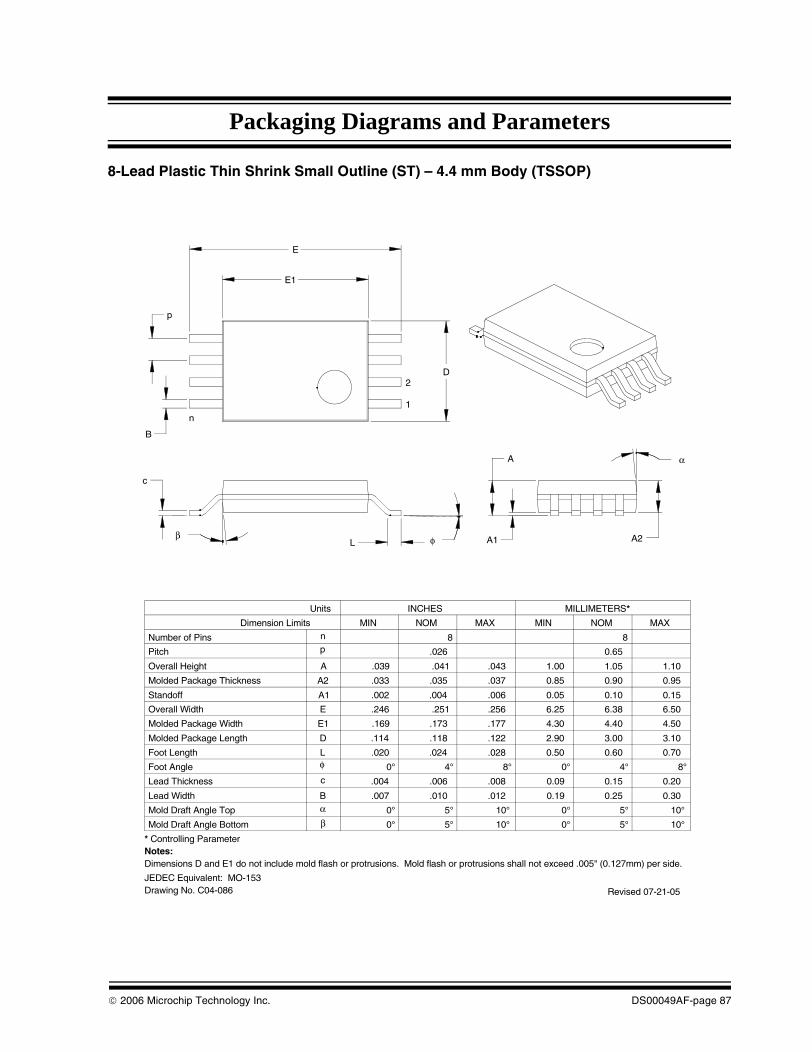
Packaging Diagrams and Parameters
8-Lead Plastic Thin Shrink Small Outline (ST) – 4.4 mm Body (TSSOP)
α
A2
A
A1L
c
β φ
1
2D
n
p
B
E
E1
10°5°0°10°5°0°βMold Draft Angle Bottom
10°5°0°10°5°0°αMold Draft Angle Top
0.300.250.19.012.010.007BLead Width
0.200.150.09.008.006.004cLead Thickness
0.700.600.50.028.024.020LFoot Length
3.103.002.90.122.118.114DMolded Package Length
4.504.404.30.177.173.169E1Molded Package Width
6.506.386.25.256.251.246EOverall Width
0.150.100.05.006.004.002A1Standoff
0.950.900.85.037.035.033A2Molded Package Thickness
1.101.051.00.043.041.039AOverall Height
0.65.026pPitch
88nNumber of Pins
MAXNOMMINMAXNOMMINDimension Limits
MILLIMETERS*INCHESUnits
Foot Angle φ 0° 4° 8° 0° 4° 8°
Dimensions D and E1 do not include mold flash or protrusions. Mold flash or protrusions shall not exceed .005" (0.127mm) per side.Notes:
JEDEC Equivalent: MO-153
Revised 07-21-05
* Controlling Parameter
Drawing No. C04-086
© 2006 Microchip Technology Inc. DS00049AF-page 87

Packaging Diagrams and Parameters
14-Lead Plastic Thin Shrink Small Outline (ST) – 4.4 mm Body (TSSOP)
Lβ
c φ
2
1
D
nB
p
E1
E
α
A2A1
A
8°4°0°8°4°0°φFoot Angle
βMold Draft Angle Bottom
12° REFαMold Draft Angle Top
0.300.250.19.012.010.007BLead Width
0.200.150.09.008.006.004cLead Thickness
0.700.600.50.028.024.020LFoot Length
5.105.004.90.201.197.193DMolded Package Length
4.504.404.30.177.173.169E1Molded Package Width
6.506.386.25.256.251.246EOverall Width
0.150.100.05.006.004.002A1Standoff
0.950.900.85.037.035.033A2Molded Package Thickness
1.101.051.00.043.041.039AOverall Height
0.65 BSC.026 BSCpPitch
1414nNumber of Pins
MAXNOMMINMAXNOMMINDimension Limits
MILLIMETERS*INCHESUnits
Dimensions D and E1 do not include mold fla sh or protrusions. Mold flash or protrusions shall not exceed .005" (0.127mm) per side.Notes:
JEDEC Equivalent: MO-153 AB-1
Revised: 08-17-05
* Controlling Parameter
BSC: Basic Dimension. Theoretically exact value shown without tolerances.
REF: Reference Dimension, usually without tole rance, for information purposes only.See ASME Y14.5M
See ASME Y14.5M
Drawing No. C04-087
12° REF
12° REF
12° REF
DS00049AF-page 88 © 2006 Microchip Technology Inc.

Packaging Diagrams and Parameters
20-Lead Plastic Thin Shrink Small Outline (ST) – 4.4 mm Body (TSSOP)
Foot Angle φ 0 4 8 0 4 8
10501050βMold Draft Angle Bottom10501050αMold Draft Angle Top
0.300.250.19.012.010.007BLead Width0.200.150.09.008.006.004cLead Thickness
0.700.600.50.028.024.020LFoot Length6.606.506.40.260.256.252DMolded Package Length4.504.404.30.177.173.169E1Molded Package Width6.506.386.25.256.251.246EOverall Width0.150.100.05.006.004.002A1Standoff §0.950.900.85.037.035.033A2Molded Package Thickness1.10.043AOverall Height
0.65.026pPitch2020nNumber of Pins
MAXNOMMINMAXNOMMINDimension LimitsMILLIMETERS*INCHESUnits
1
2
D
p
n
B
E1
E
Lβ
c
φ
α
A2
A1
A
* Controlling Parameter
Notes:Dimensions D and E1 do not include mold flash or protrusions. Mold flash or protrusions shall not exceed .005” (0.127mm) per side.
JEDEC Equivalent: MO-153Drawing No. C04-088
§ Significant Characteristic
p
© 2006 Microchip Technology Inc. DS00049AF-page 89

Packaging Diagrams and Parameters
NOTES:
DS00049AF-page 90 © 2006 Microchip Technology Inc.

Packaging Diagrams and Parameters
28-Lead Plastic Thin Small Outline (TS) – 5 x 20 mm Body (TSOP)
.020
A1
A
A2
α
φβ
c
L
E
p
Bn
D
12
Units INCHES MILLIMETERS*Dimension Limits MIN NOM MAX MIN NOM MAX
Number of Pins n 28 28Pitch p 0.50Overall Height A .051 1.30Molded Package Thickness A2 .037 .039 .041 0.95 1.00 1.05Standoff § A1 .002 .006 .010 0.05 0.15 0.25Overall Width E .780 .787 .795 19.80 20.00 20.20Molded Package Width E1 .720 .724 .728 18.30 18.40 18.50Molded Package Length D .307 .315 .323 7.80 8.00 8.20Foot Length L .020 .024 .028 0.50 0.60 0.70
Lead Thickness c .004 .006 .008 0.10 0.15 0.20Lead Width B .006 .008 .010 0.15 0.20 0.25Mold Draft Angle Top α 0 5 10 0 5 10Mold Draft Angle Bottom β 0 5 10 0 5 10
840840φFoot Angle
3 x p
.039 .045 0.99 1.14
* Controlling Parameter
Notes:Dimensions D and E1 do not include mold flash or protrusions. Mold flash or protrusions shall not exceed .005” (0.127mm) per side.
EIAJ Equivalent: IC-74-2-3Drawing No. C04-067
§ Significant Characteristic
E1
© 2006 Microchip Technology Inc. DS00049AF-page 91

Packaging Diagrams and Parameters
28-Lead Plastic Very Small Outline (VS) – 8 x 13.4 mm Body (VSOP)
Foot Angle φ 0 3 5 0 3 5
10501050βMold Draft Angle Bottom10501050αMold Draft Angle Top
0.230.200.17.009.008.007BLead Width0.160.150.14.006.006.006cLead Thickness
0.700.500.30.028.020.012LFoot Length8.108.007.90.319.315.311DMolded Package Length
11.9011.8011.70.469.465.461E1Molded Package Width13.6013.4013.20.535.528.520EOverall Width
0.05.002A1Standoff §1.051.000.95.041.039.037A2Molded Package Thickness1.29.051AOverall Height
0.55.022pPitch2828nNumber of Pins
MAXNOMMINMAXNOMMINDimension LimitsMILLIMETERS*INCHESUnits
A2
α
A
A1Lβ
c
φ
12
nD
p
B
E
E1
.045
.005 .010
1.14
0.13 0.25
.039 0.99
* Controlling Parameter
Notes:Dimensions D and E1 do not include mold flash or protrusions. Mold flash or protrusions shall not exceed .005” (0.127mm) per side. Drawing No. C04-075
§ Significant Characteristic
DS00049AF-page 92 © 2006 Microchip Technology Inc.

Packaging Diagrams and Parameters
32-Lead Plastic Low-Profile Quad Flatpack (PL) 7x7x1.4 mm Body, 1.0/0.10 mm Lead Form (LQFP)
.039 REF.FFootprint
Units INCHES MILLIMETERS*
Dimension Limits MIN NOM MAX MIN NOM MAX
Number of Pins N 32 32
Pitch e .031 BSC. 0.80 BSC
Overall Height A - - .063 - - 1.60
Molded Package Thickness A2 .053 .055 .057 1.35 1.40 1.45
Standoff A1 .002 - .006 0.05 - 0.15
Foot Length L .018 .024 .030 0.45 0.60 0.75
Foot Angle φ 0° 3.5° 7° 0° 3.5° 7°
Overall Width E .354 BSC. 9.00 BSC.
Overall Length D .354 BSC. 9.00 BSC.
Molded Package Width E1 .276 BSC. 7.00 BSC.
Molded Package Length D1 .276 BSC. 7.00 BSC.
Lead Thickness c .004 - .008 0.09 - 0.20
Lead Width b .012 .015 .018 0.30 0.37 0.45
Mold Draft Angle Top α 11° 12° 13°
Mold Draft Angle Bottom β 11° 12° 13°
Dimensions D1 and E1 do not include mold flash or protrusions. Mold flash or protrusions shall not exceed .010" (0.254mm) per side.Notes:
JEDEC Equivalent: MS-026 BBA Revised 08-26-05
* Controlling Parameter
1.00 REF.
11°
11° 13°
13°
12°
12°
BSC: Basic Dimension. Theoretically exact value shown without tolerances.
REF: Reference Dimension, usually without tolerance, for information purposes only.See ASME Y14.5M
See ASME Y14.5M
1. Pin 1 visual feature may vary, but must be located within the hatched area.2. Chamfers at corners are optional; size may vary
D
1 2
Nb
e
E1 E
D1
Note 1
c
L A1
A2
A
β
α
φ
F
Note 2
Drawing No. C04-045
© 2006 Microchip Technology Inc. DS00049AF-page 93
Packaging Diagrams and Parameters
NOTES:
DS00049AF-page 94 © 2006 Microchip Technology Inc.
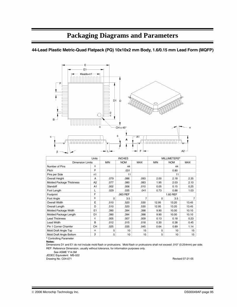
Packaging Diagrams and Parameters
44-Lead Plastic Metric-Quad Flatpack (PQ) 10x10x2 mm Body, 1.6/0.15 mm Lead Form (MQFP)
21
n
D1 D
B
p
E
E1
#leads=n1
c
β
φ
α
A2
A
CH x 45°
L F
A1
1510515105βMold Draft Angle Bottom
1510515105αMold Draft Angle Top
0.450.380.30.018.015.012BLead Width
0.230.180.13.009.007.005cLead Thickness
1111n1Pins per Side
10.1010.009.90.398.394.390D1Molded Package Length
10.1010.009.90.398.394.390E1Molded Package Width
13.4513.2012.95.530.520.510DOverall Length
13.4513.2012.95.530.520.510EOverall Width
73.5073.50φFoot Angle
1.030.880.73.041.035.029LFoot Length
0.250.150.05.010.006.002A1Standoff
2.102.031.95.083.080.077A2Molded Package Thickness
2.35.093AOverall Height
0.80.031pPitch
4444nNumber of Pins
MAXNOMMINMAXNOMMINDimension Limits
MILLIMETERS*INCHESUnits
Pin 1 Corner Chamfer
Footprint F
CH .025 .035 .045 0.64 0.89 1.14
Dimensions D1 and E1 do not include mold flash or protrusions. Mold flash or protrusions shall not exceed .010" (0.254mm) per side.Notes:
JEDEC Equivalent: MS-022Revised 07-21-05
* Controlling Parameter
.079 .086 2.00 2.18
REF: Reference Dimension, usually without tolerance, for information purposes only.See ASME Y14.5M
Drawing No. C04-071
1.60 REF.063 REF
A
© 2006 Microchip Technology Inc. DS00049AF-page 95

Packaging Diagrams and Parameters
64-Lead Metric-Quad Flatpack (KU) 14x14x2.7 mm Body, 1.6/0.25 mm Lead Form (MQFP)
D
E1
e
B
c
2
n
1
A
A1A2
E
D1
φ
α
FβL
§ Significant Characteristic
Revised 07-21-05
Notes:
Dimensions D1 and E1 do not include mold flash or protrusions. Mold flash or protrusions shall not exceed .010" (0.254mm) per side.
JEDEC equivalent: MS-022 BE.
* Controlling Parameter
.063 REFFFootprint
Mold Draft Angle Top
Mold Draft Angle Bottom
Foot Angle
Lead Width
Lead Thickness
βα
c
B
φ
.004
0°
Dimension Limits
Overall Height
Molded Package Thickness
Molded Package Width
Molded Package Length
Foot Length
Standoff §
Overall Width
Number of Pins
Pitch
A
L
E1
D1
A1
E
A2
.029 .035
.551 BSC
.551 BSC
.000
.098
.677 BSC
.106
MIN
e
n
Units
.031 BSC
NOM
64
INCHES
1.60 REF
.009
6°
0.11
0°
0.23
7°
MILLIMETERS*
0.80 BSC
2.70
14.00 BSC
14.00 BSC
0.88
17.20 BSC
.124
.041
.114
.010
0.73
0.00
2.50
MINMAX NOM
3.15
1.03
0.25
2.90
MAX
64
5°
5° 16° 5° 16°
16° 5° 16°
Overall Length D .677 BSC 17.20 BSC
0.450.29.018.011
Formerly TelCom PQFP package.
2.50 --.098 --
-- --
----
----
----
----
----
BSC: Basic Dimension. Theoretically exact value shown without tolerances.
REF: Reference Dimension, usually without tolerance, for information purposes only.See ASME Y14.5M
See ASME Y14.5M
Drawing No. C04-022
DS00049AF-page 96 © 2006 Microchip Technology Inc.

Packaging Diagrams and Parameters
44-Lead Plastic Quad Flatpack (KW) 10x10x2.0 mm Body, 1.95/0.25 mm Lead Form (PQFP)
CHAMFER VARIES
D
E1
E
p
c
B
D1
n
L
21
FA1
AA2
α
β
φ
1.95 REF..077 REF.FFootprint
Units INCHES MILLIMETERS*
Dimension Limits MIN NOM MAX MIN NOM MAX
Number of Pins n 44 44
Pitch p .031 BSC 0.80 BSC
Overall Height A - - .096 - - 2.45
Molded Package Thickness A2 .077 .079 .083 1.95 2.00 2.10
Standoff § A1 .010 - - 0.25 - -
Foot Length L .029 .035 .041 0.73 0.88 1.03
Foot Angle φ 0° 3.5° 7° 0° 3.5° 7°
Overall Width E .547 BSC 13.90 BSC
Overall Length D .547 BSC 13.90 BSC
Molded Package Width E1 .394 BSC 10.00 BSC
Molded Package Length D1 .394 BSC 10.00 BSC
Lead Thickness c .004 - .009 0.11 - 0.23
Lead Width B .012 - .018 0.30 - 0.45
Mold Draft Angle Top α 5° - 16° 5° - 16°
Mold Draft Angle Bottom β 5° - 16° 5° - 16°
Dimensions D and E1 do not include mold flash or protrusions. Mold flash or protrusions shall not exceed .010" (0.254mm) per side.Notes:
JEDEC Equivalent: MO-112 AA-1 Revised 07-21-05
* Controlling Parameter§ Significant Characteristic
BSC: Basic Dimension. Theoretically exact value shown without tolerances.
REF: Reference Dimension, usually without tolerance, for information purposes only.See ASME Y14.5M
See ASME Y14.5M
Drawing No. C04-119
© 2006 Microchip Technology Inc. DS00049AF-page 97

Packaging Diagrams and Parameters
NOTES:
DS00049AF-page 98 © 2006 Microchip Technology Inc.

Packaging Diagrams and Parameters
32-Lead Thin-Quad Flatpack (PT) 7x7x1.0 mm Body, 1.0/0.10 mm Lead Form (TQFP)
1.00 REF.039 REFFFootprint
Units INCHES MILLIMETERS*
Dimension Limits MIN NOM MAX MIN NOM MAX
Number of Leads N 32 32
Lead Pitch e .031 BSC 0.80 BSC
Overall Height A – – .047 – – 1.20
Standoff A1 .002 – .006 0.05 – 0.15
Molded Package Thickness A2 .037 .039 .041 0.95 1.00 1.05
Foot Length L .018 .024 .030 0.45 0.60 0.75
Foot Angle φ 0° 3.5° 7° 0° 3.5° 7°
Overall Width E .354 BSC 9.00 BSC
Overall Length D .354 BSC 9.00 BSC
Molded Package Width E1 .276 BSC 7.00 BSC
Molded Package Length D1 .276 BSC 7.00 BSC
Leads per Side 8 8
Lead Thickness c .004 .006 .008 0.09 0.15 0.20
Lead Width b .012 .015 .017 0.30 0.37 0.45
Mold Draft Angle Top α 11° 12° 13° 11° 12° 13°
Mold Draft Angle Bottom β 11° 12° 13° 11° 12° 13°
Dimensions D1 and E1 do not include mold flash or protrusions. Mold flash or protrusions shall not exceed .010" (0.254mm) per side.Notes:
JEDEC Equivalent: MS-026 ABARevised 09-15-05
* Controlling Parameter
REF: Reference Dimension, usually without tolerance, for information purposes only.See ASME Y14.5M
BSC: Basic Dimension. Theoretically exact value shown without tolerances.See ASME Y14.5M
1. Pin 1 visual index feature may vary, but must be located within the hatched area.2. Chamfers at corners are optional; size may vary.
D1
D
EE1
1 2 3
N
c φ
L F
A2
A1
A
e
b
α
β
NOTE 1
NOTE 2
Drawing No. C04-074
© 2006 Microchip Technology Inc. DS00049AF-page 99

Packaging Diagrams and Parameters
44-Lead Plastic Thin-Quad Flatpack (PT) 10x10x1 mm Body, 1.0/0.10 mm Lead Form (TQFP)
F
A
A1 A2
α
E
E1
#leads=n1
p
B
D1 D
n
12
φ
c
βL
CH x 45°
1.140.890.64.045.035.025CHPin 1 Corner Chamfer
1.00 REF..039 REF.FFootprint (Reference)
Units INCHES MILLIMETERS*Dimension Limits MIN NOM MAX MIN NOM MAX
Number of Pins n 44 44
Pitch p .031 0.80
Overall Height A .039 .043 .047 1.00 1.10 1.20
Molded Package Thickness A2 .037 .039 .041 0.95 1.00 1.05
Standoff A1 .002 .004 .006 0.05 0.10 0.15
Foot Length L .018 .024 .030 0.45 0.60 0.75
Foot Angle φ 0 3.5 7 0 3.5 7
Overall Width E .463 .472 .482 11.75 12.00 12.25
Overall Length D .463 .472 .482 11.75 12.00 12.25
Molded Package Width E1 .390 .394 .398 9.90 10.00 10.10
Molded Package Length D1 .390 .394 .398 9.90 10.00 10.10
Pins per Side n1 11 11
Lead Thickness c .004 .006 .008 0.09 0.15 0.20
Lead Width B .012 .015 .017 0.30 0.38 0.44
Mold Draft Angle Top α 5 10 15 5 10 15
Mold Draft Angle Bottom β 5 10 15 5 10 15
Dimensions D and E1 do not include mold flash or protrusions. Mold flash or protrusions shall not exceed .010" (0.254mm) per side.Notes:
JEDEC Equivalent: MS-026Revised 07-22-05
* Controlling Parameter
REF: Reference Dimension, usually without tolerance, for information purposes only.See ASME Y14.5M
Drawing No. C04-076
DS00049AF-page 100 © 2006 Microchip Technology Inc.

Packaging Diagrams and Parameters
64-Lead Plastic Thin-Quad Flatpack (PT) 10x10x1 mm Body, 1.0/0.10 mm Lead Form (TQFP)
1510515105βMold Draft Angle Bottom
1510515105αMold Draft Angle Top
0.270.220.17.011.009.007BLead Width
0.230.180.13.009.007.005cLead Thickness
1616n1Pins per Side
10.1010.009.90.398.394.390D1Molded Package Length
10.1010.009.90.398.394.390E1Molded Package Width
12.2512.0011.75.482.472.463DOverall Length
12.2512.0011.75.482.472.463EOverall Width
73.5073.50φFoot Angle
0.750.600.45.030.024.018LFoot Length
0.250.150.05.010.006.002A1Standoff
1.051.000.95.041.039.037A2Molded Package Thickness
1.201.101.00.047.043.039AOverall Height
0.50.020pPitch
6464nNumber of Pins
MAXNOMMINMAXNOMMINDimension Limits
MILLIMETERS*INCHESUnits
Footprint F .039 REF. 1.00 REF.
Pin 1 Corner Chamfer CH .025 .035 .045 0.64 0.89 1.14
REF: Reference Dimension, usually without tolerance, for information purposes only.
Revised 07-22-05
Dimensions D and E1 do not include mold flash or protrusions. Mold flash or protrusions shall not exceed .010" (0.254mm) per side.
See ASME Y14.5M
* Controlling Parameter
JEDEC Equivalent: MS-026
Notes:
c
21
n
DD1
B
p
#leads=n1
E1
E
A2A1
A
L
CH x 45°
β
φ
α
F
Drawing No. C04-085
© 2006 Microchip Technology Inc. DS00049AF-page 101

Packaging Diagrams and Parameters
64-Lead Plastic Thin-Quad Flatpack (PT) 14x14x1 mm Body, 1.0/0.10 mm Lead Form (TQFP)
A2
a
A1A
c
(F)L
fb
D
E
#leads=n1
E1
p
B
D1
n
12
Dimensions D1 and E1 do not include mold flash or protrusions. Mold flash or protrusions shall not exceed .010" (0.254mm) per side.
.630 BSC
NOM
INCHES
.630 BSC
.551 BSC
.551 BSC
Overall Width
Overall Length
Foot Angle
Foot Length
Pins per Side
Overall Height
Number of Pins
Lead Width
Drawing No. C04-066
Lead Thickness
Molded Package Thickness
* Controlling Parameter
JEDEC Equivalent: MS-026
Mold Draft Angle Bottom
Mold Draft Angle Top
Molded Package Width
Molded Package Length
Footprint
Notes:
Pitch
Standoff
11β
Dimension Limits
αB
D1
E1
c
φ
D
E
(F)
L
11
.012
.004
.018
0
MIN
A
A1
A2
n1
p
Units
n
.037
.002
121112 13
12
.015
3.5
.039 REF
.024
.018
.008
13
.030
7
16
.031 BSC
.039
64
.041
.006
.047
MAX
16.00 BSC
16.00 BSC
14.00 BSC
14.00 BSC
0.30
0.09
11
0.45
0
0.37
12
1.00 REF
0.60
3.5
MILLIMETERS*
0.95
0.05
MIN
0.80 BSC
1.00
16
NOM
64
13
0.45
0.20
13
0.75
7
1.05
0.15
1.20
MAX
Revised 09-14-05
BSC: Basic Dimension. Theoretically exact value shown without tolerances. See ASME Y14.5M
DS00049AF-page 102 © 2006 Microchip Technology Inc.

Packaging Diagrams and Parameters
80-Lead Plastic Thin-Quad Flatpack (PT) 12x12x1 mm Body, 1.0/0.10 mm Lead Form (TQFP)
F
EE1
#leads=n1
p
B
D1 D
n
12
φ
c
βL
A
A1 A2
αCH x 45°
1.101.00.043.039
1.140.890.64.045.035.025CHPin 1 Corner Chamfer
1.00 REF..039 REF.FFootprint
Units INCHES MILLIMETERS*Dimension Limits MIN NOM MAX MIN NOM MAX
Number of Pins n 80 80
Pitch p .020 BSC 0.50 BSC
Overall Height A .047 1.20
Molded Package Thickness A2 .037 .039 .041 0.95 1.00 1.05
Standoff A1 .002 .004 .006 0.05 0.10 0.15
Foot Length L .018 .024 .030 0.45 0.60 0.75
Foot Angle φ 0° 3.5° 7° 0° 3.5° 7°
Overall Width E .551 BSC 14.00 BSC
Overall Length D .551 BSC 14.00 BSC
Molded Package Width E1 .472 BSC 12.00 BSC
Molded Package Length D1 .472 BSC 12.00 BSC
Pins per Side n1 20 20
Lead Thickness c .004 .006 .008 0.09 0.15 0.20
Lead Width B .007 .009 .011 0.17 0.22 0.27
Mold Draft Angle Top α 5° 10° 15° 5° 10° 15°
Mold Draft Angle Bottom β 5° 10° 15° 5° 10° 15°
Notes:
JEDEC Equivalent: MS-026Revised 07-22-05
* Controlling Parameter
REF: Reference Dimension, usually without tolerance, for information purposes only.
BSC: Basic Dimension. Theoretically exact value shown without tolerances.
Dimensions D1 and E1 do not include mold flash or protrusions. Mold flash or protrusions shall not exceed .010" (0.254mm) per side.
See ASME Y14.5M
See ASME Y14.5M
Drawing No. C04-092
© 2006 Microchip Technology Inc. DS00049AF-page 103

Packaging Diagrams and Parameters
80-Lead Plastic Thin-Quad Flatpack (PF) 14x14x1 mm Body, 1.0/0.10 mm Lead Form (TQFP)
D
E1
#leads=n1
p
B
L
φ
β
c
2
n
1
(F)
A
A1
α
A2
E
D1
Dimensions D1 and E1 do not include mold flash or protrusions. Mold flash or protrusions shall not exceed .010" (0.254mm) per side.
.630 BSC
NOM
INCHES
.630 BSC
.551 BSC
.551 BSC
Overall Width
Overall Length
Foot Angle
Foot Length
Pins per Side
Overall Height
Number of Pins
Lead Width
Revised 09-16-05
Lead Thickness
Molded Package Thickness
* Controlling Parameter
JEDEC Equivalent: MS-026
Mold Draft Angle Bottom
Mold Draft Angle Top
Molded Package Width
Molded Package Length
Footprint
Notes:
Pitch
Standoff
β
Dimension Limits
αB
D1
E1
c
φ
D
E
F
L
11°
.011
.004
.018
0°
MIN
A
A1
A2
n1
p
Units
n
.037
.002
12°
.013
3.5°
.039 REF.
.024
.015
.008
13°
.030
7°
20
.026
.039
80
.041
.006
.047
MAX
16.00 BSC
16.00 BSC
14.00 BSC
14.00 BSC
0.27
0.09
0.45
0°
0.32
1.00 REF.
0.60
3.5°
MILLIMETERS*
0.95
0.05
MIN
0.65
1.00
20
NOM
80
0.37
0.20
0.75
7°
1.05
0.15
1.20
MAX
13°12°11°
12°11° 11°13° 12° 13°
REF: Reference Dimension, usually without tolerance, for information purposes only.
BSC: Basic Dimension. Theoretically exact value shown without tolerances.
See ASME Y14.5M
See ASME Y14.5M
Drawing No. C04-116
DS00049AF-page 104 © 2006 Microchip Technology Inc.

Packaging Diagrams and Parameters
100-Lead Plastic Thin-Quad Flatpack (PT) 12x12x1 mm Body, 1.0/0.10 mm Lead Form (TQFP)
F
EE1
#leads=n1
B
D1 D
n
12
φ
c
β L
A
A1A2
αCH x 45°
p
1.101.00.043.039
1.00 REF..039 REF.FFootprint (Reference)
Units INCHES MILLIMETERS*
Dimension Limits MIN NOM MAX MIN NOM MAX
Number of Pins n 100 100
Pitch p .016 BSC 0.40 BSC
Overall Height A .047 1.20
Molded Package Thickness A2 .037 .039 .041 0.95 1.00 1.05
Standoff A1 .002 .004 .006 0.05 0.10 0.15
Foot Length L .018 .024 .030 0.45 0.60 0.75
Foot Angle φ 0° 3.5° 7° 0° 3.5° 7°
Overall Width E .551 BSC 14.00 BSC
Overall Length D .551 BSC 14.00 BSC
Molded Package Width E1 .472 BSC 12.00 BSC
Molded Package Length D1 .472 BSC 12.00 BSC
Pins per Side n1 25 25
Lead Thickness c .004 .006 .008 0.09 0.15 0.20
Lead Width B .005 .007 .009 0.13 0.18 0.23
Mold Draft Angle Top α 5° 10° 15° 5° 10° 15°
Mold Draft Angle Bottom β 5° 10° 15° 5° 10° 15°
Dimensions D1 and E1 do not include mold flash or protrusions. Mold flash or protrusions shall not exceed .010" (0.254mm) per side.Notes:
JEDEC Equivalent: MS-026
* Controlling Parameter
BSC: Basic Dimension. Theoretically exact value shown without tolerances.
REF: Reference Dimension, usually without tolerance, for information purposes only.See ASME Y14.5M
See ASME Y14.5MRevised 07-22-05
Drawing No. C04-100
© 2006 Microchip Technology Inc. DS00049AF-page 105

Packaging Diagrams and Parameters
100-Lead Plastic Thin-Quad Flatpack (PF) 14x14x1 mm Body, 1.0/0.10 mm Lead Form (TQFP)
D
D1
E
E1
#leads=n1
p
B
L
φ
βc
2
n
1
F
A
A1
α
A2
Dimensions D1 and E1 do not include mold flash or protrusions. Mold flash or protrusions shall not exceed .010" (0.254mm) per side.
.630 BSC
NOM
INCHES
.630 BSC
.551 BSC
.551 BSC
Overall Width
Overall Length
Foot Angle
Foot Length
Pins per Side
Overall Height
Number of Pins
Lead Width
Revised 07-21-05
Lead Thickness
Molded Package Thickness
* Controlling Parameter
JEDEC Equivalent: MS-026
Mold Draft Angle Bottom
Mold Draft Angle Top
Molded Package Width
Molded Package Length
Footprint
Notes:
Pitch
Standoff
11°β
Dimension Limits
αB
D1
E1
c
φ
D
E
F
L
11°
.007
.004
.018
0°
MIN
A
A1
A2
n1
p
Units
n
.037
.002
12°11°12° 13°
12°
.009
3.5°
.039 REF
.024
.011
.008
13°
.030
7°
25
.020 BSC
.039
100
.041
.006
.047
MAX
16.00 BSC
16.00 BSC
14.00 BSC
14.00 BSC
0.17
0.09
11°
0.45
0°
0.22
12°
1.00 REF
0.60
3.5°
MILLIMETERS*
0.95
0.05
MIN
0.50 BSC
1.00
25
NOM
100
13°
0.27
0.20
13°
0.75
7°
1.05
0.15
1.20
MAX
REF: Reference Dimension, usually without tolerance, for information purposes only.
BSC: Basic Dimension. Theoretically exact value shown without tolerances.
See ASME Y14.5M
See ASME Y14.5M
Drawing No. C04-110
DS00049AF-page 106 © 2006 Microchip Technology Inc.

PACKAGINGProduct Tape and Reel Specifications
FIGURE 1: EMBOSSED CARRIER DIMENSIONS (8, 12, 16, AND 24 MM TAPE ONLY)
TopCoverTape
K0
P
W
B0
A0
TABLE 1: CARRIER TAPE/CAVITY DIMENSIONS
CaseOutline
Package Type
CarrierDimensions
CavityDimensions Output
QuantityUnits
ReelDiameter in
mmWmm
Pmm
A0mm
B0mm
K0mm
SN SOIC .150” 8L 12 8 6.4 5.2 2.1 3300 330
SO SOIC .300” 16L 16 12 10.9 10.7 3.0 1000 330
SO SOIC .300” 18L 2424
1216
10.911.1
13.312.0
3.02.8
16001100
330330
SO SOIC .300” 20L 24 12 10.9 13.3 3.0 1600 330
SO SOIC .300” 24L 24 12 10.9 16.0 3.0 1000 330
SO SOIC .300” 28L 2424
1212
10.911.1
18.318.5
3.03.0
16001600
330330
L PLCC 28L 24 16 13.0 13.0 4.9 750 330
L PLCC 32L 24 16 13.1 15.5 3.9 900 330
L PLCC 44L 3232
2424
18.018.0
18.018.0
4.95.0
500500
330
L PLCC 68L 44 32 25.6 25.6 5.8 300 330
L PLCC 84L 44 36 30.7 30.7 5.8 200 330
SM SOIC .208” 8L 16 12 8.3 5.7 2.3 2100 330
SL SOIC .150” 14L 16 8 6.5 9.5 2.1 2600 330
SL SOIC .150” 16L 16 8 6.5 10.3 2.1 2600 330
TS TSOP 28L/32L 32 16 8.6 20.6 2.1 1500 330
SS SSOP 20L 16 12 8.4 7.7 2.5 1600 330
SS SSOP 28L 24 12 8.4 10.9 2.4 2100 330
PQ MQFP 44L 24 24 14.2 14.2 2.8 900 330
PT TQFP 44L/64L 24 16 12.4 12.4 2.2 1200 330
VS VSOP 28L 24 12 8.7 13.9 2.1 2500 330
© 2006 Microchip Technology Inc. DS00049AF-page 107
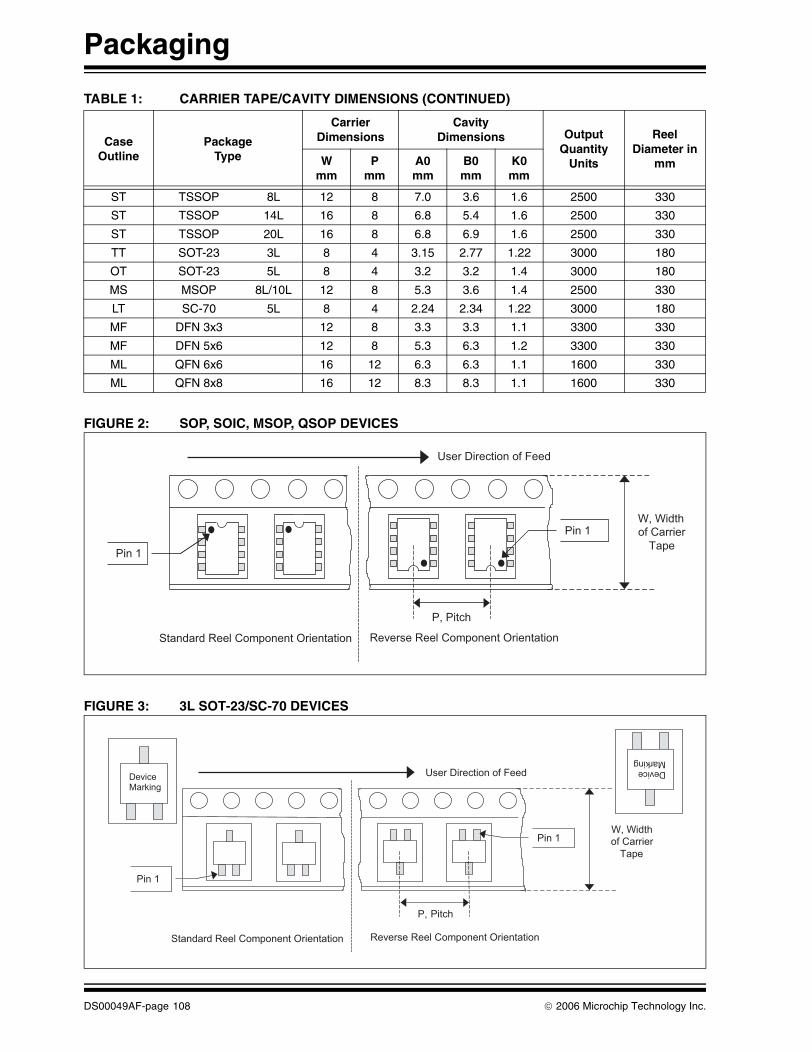
Packaging
FIGURE 2: SOP, SOIC, MSOP, QSOP DEVICES
FIGURE 3: 3L SOT-23/SC-70 DEVICES
ST TSSOP 8L 12 8 7.0 3.6 1.6 2500 330
ST TSSOP 14L 16 8 6.8 5.4 1.6 2500 330
ST TSSOP 20L 16 8 6.8 6.9 1.6 2500 330
TT SOT-23 3L 8 4 3.15 2.77 1.22 3000 180
OT SOT-23 5L 8 4 3.2 3.2 1.4 3000 180
MS MSOP 8L/10L 12 8 5.3 3.6 1.4 2500 330
LT SC-70 5L 8 4 2.24 2.34 1.22 3000 180
MF DFN 3x3 12 8 3.3 3.3 1.1 3300 330
MF DFN 5x6 12 8 5.3 6.3 1.2 3300 330
ML QFN 6x6 16 12 6.3 6.3 1.1 1600 330
ML QFN 8x8 16 12 8.3 8.3 1.1 1600 330
TABLE 1: CARRIER TAPE/CAVITY DIMENSIONS (CONTINUED)
CaseOutline
Package Type
CarrierDimensions
CavityDimensions Output
QuantityUnits
ReelDiameter in
mmWmm
Pmm
A0mm
B0mm
K0mm
User Direction of Feed
P, Pitch
Pin 1
Pin 1
Reverse Reel Component Orientation
W, Width
of Carrier
Tape
Standard Reel Component Orientation
User Direction of Feed
P,
Pitch
Standard Reel Component Orientation Reverse Reel Component Orientation
W, Width
of Carrier
Tape
Pin 1
Pin 1
DeviceMarking
DeviceMarking
DS00049AF-page 108 © 2006 Microchip Technology Inc.

Packaging
FIGURE 4: 5L SOT-23/SC-70 DEVICES
FIGURE 5: 6L SOT-23 DEVICES
User Direction of Feed
P, Pitch
Standard Reel Component Orientation Reverse Reel Component Orientation
W, Width
of Carrier
Tape
Pin 1
Pin 1
DeviceMarking
Pin 1
User Direction of Feed
Standard Reel Component Orientation Reverse Reel Component Orientation
W, Width
of Carrier
Tape
Pin 1
DeviceMarking
P, Pitch
© 2006 Microchip Technology Inc. DS00049AF-page 109

Packaging
FIGURE 6: 3L SOT-223 DEVICES
FIGURE 7: PLCC DEVICES
Pin 1
User Direction of Feed
P, Pitch
Standard Reel Component Orientation Reverse Reel Component Orientation
W, Width
of CarrierTape
Pin 1
DeviceMarking
User Direction of Feed
P, Pitch
Standard Reel Component Orientation Reverse Reel Component Orientation
W, Width
of CarrierTape
Pin 1
Pin 1
DS00049AF-page 110 © 2006 Microchip Technology Inc.

Packaging
FIGURE 8: MQFP DEVICES
FIGURE 9: 4L SOT-143 DEVICES
User Direction of Feed
P, Pitch
Standard Reel Component Orientation Reverse Reel Component Orientation
W, Width
of Carrier
TapePin 1
Pin 1
DeviceMarking
P, Pitch
W, Width
of Carrier
Tape
User Direction of Feed
Pin 1
Standard Reel Component Orientation Reverse Reel Component Orientation
Pin 1
© 2006 Microchip Technology Inc. DS00049AF-page 111

Packaging
FIGURE 10: 3L/5L/7L DDPAK AND 3L DPAK DEVICES
FIGURE 11: SOT-89 DEVICES
FIGURE 12: DFN/QFN DEVICES
P, Pitch
Standard Reel Component Orientation Reverse Reel Component Orientation
Leaded
side should
be placed
toward
sprocket
hole Leaded side
should be placed
opposite to
sprocket hole
User Direction of Feed
W, Width
of Carrier
Tape
Device
Marking
Pin 1
User Direction of Feed
P, Pitch
Standard Reel Component Orientation Reverse Reel Component Orientation
W, Width
of Carrier
TapePin 1
User Direction of Feed
Pin 1
DS00049AF-page 112 © 2006 Microchip Technology Inc.

Packaging
FIGURE 13: TO-92 DEVICES
3 LEAD
TO-92
2 LEAD
TO-92
Device
Marking
Device
Marking
P, Pitch
W, Width of
Carrier Tape
W, Width of
Carrier Tape
Standard Reel
Component Orientation
Reverse Reel
Component Orientation
W6
F
P1F2
P2
F1D
H1
HH0
© 2006 Microchip Technology Inc. DS00049AF-page 113

Packaging
DIMENSIONS AND TOLERANCES
All component taping diagrams, dimensions, toler-ances and component positioning requirements arethose which are specified per EIA Standard EIA-481,current revision.
For the 8-lead SOIC EIAJ Type II Package and 16 mmCarrier Tape width, the component taping diagrams,dimensions and tolerances and component positioningrequirements are those which are specified per EIAJStandard RC-1009B, current revision.
DS00049AF-page 114 © 2006 Microchip Technology Inc.

PACKAGINGThermal Characteristics
THERMAL CHARACTERISTICS
Characteristic Symbol Value Unit
Average Junction Temperature TJ TA + (PD x Θja) °C
Ambient Temperature TA User Determined °C
Total Power Dissipation1 PD PINT + PI/O W
Device Internal Power Dissipation PINT IDD X VDD W
I/O Pin Power Dissipation PI/O User Determined W
© 2006 Microchip Technology Inc. DS00049AF-page 115

Packaging
THERMAL RESISTANCE
Note 1: Approximate value, disregarding PI/O.
2: All thermal resistance values are estimated and are dependent on die and materials used. Variables includedie and leadframe paddle sizes. Relative values are taken in still air.
Item Leads Package Package BodyΘJc
(°C/W)ΘJa
(°C/W)
Package ThermalResistance(2)
8 PDIP .300” 41.2 84.6
14 PDIP .300” 32.5 69.8
16 PDIP .300” 34.1 69.9
18 PDIP .300” 29.4 65.9
20 PDIP .300” 28.1 62.4
24 PDIP .600” 21 63
28 PDIP .600” 31.4 59.1
28 SPDIP .300” 29 60
40 PDIP .600” 24.7 47.2
8 SOIC .150” 38.8 163
8 SOIC .208” 27.98 117.55
16 SOIC .300” 24.8 89.6
18 SOIC .300” 24.6 63.6
20 SOIC .300” 24.2 85.2
28 SOIC .300” 23.8 80.2
8 MSOP .118” 39.1 206.3
8 TSSOP 4.4 mm 36.6 123.7
14 TSSOP 4.4 mm 31.7 100.4
20 TSSOP 4.4 mm 17 90.2
28 TSSOP 4.4 mm 13.3 75.5
20 SSOP .209” 32.2 108.1
28 SSOP .209” 23.9 89.4
3 SOT-23 110.12 336
5 SOT-23 81 255.9
3 TO-92 66.3 131.9
20 PLCC 37.6 62.5
28 PLCC 25.4 50.4
32 PLCC 22.7 52.4
44 PLCC 20.6 45.4
68 PLCC 16.1 39.3
84 PLCC 11.4 35.8
44 TQFP 10x10x1 mm 14.5 45.79
64 TQFP 10x10x1 mm 24.4 76.6
80 TQFP 12x12x1 mm 24.4 69.4
100 TQFP 14x14x1 mm 24.4 50
44 MQFP 10x10x2 mm 14.8 57.8
DS00049AF-page 116 © 2006 Microchip Technology Inc.

PACKAGINGOverview of Microchip Die/Wafer Support
INTRODUCTION
Microchip Technology Inc. devices are available inwafer form and in die form. All products sold in die orwafers have been characterized and qualified accord-ing to the requirements of Microchip Technology Inc.Specifications SPI-41014, “Characterization andQualification of Integrated Circuits” and QCI-39000,“Worldwide Quality Conformance Requirements”.
PRODUCT INTEGRITY
Product supplied in die or wafer form are fully testedand characterized. Die or Wafers are inspected toMicrochip Technology Inc. Specification, QCI-30014.
ORDERING INFORMATION
Die sales must be conducted by contacting yourMicrochip Sales Office.
To order or obtain information (on pricing or delivery)for a specific device, use one of the following partnumbers:
Devices in Waffle PackDEVICE_NUMBER/S
Devices in Wafer formDEVICE_NUMBER/WDEVICE_NUMBER/WF
where DEVICE_NUMBER is the device that yourequire. The S specifies die in a waffle pack, while a Wspecifies wafer sales and WF specifies sawn wafer onframes.
ELECTRICAL SPECIFICATIONS
The functional and electrical specifications of Microchipdevices in die form are identical to those of a packagedversion. Please refer to individual data sheets forcomplete details.
QTP
Quick-Turnaround-Production (QTP) applies only toEPROM and EEPROM microcontrollers.
With QTP devices, the program memory array is onlytested against the code provided. This method ensuresthat the device will operate correctly as programmed,but does not ensure that every program memory bit canbe programmed to every state.
EPROM
EPROM devices are supplied as fully erasedprogrammable parts that are UV erasable and re-programmable by the user (except for QTP and SQTPdevices).
EEPROM
EEPROM devices may not be supplied in a fully erasedstate, but are reprogrammable by the user (except forQTP and SQTP devices).
ROM
ROM devices are supplied as fully programmed parts(program memory only). These are notreprogrammable by the user.
DIE MECHANICAL SPECIFICATIONS
Refer to the individual data sheet for thesespecifications.
CAUTION
Some EEPROM devices use EPROM cells fordevice configuration. Exposure to ultraviolet lightmust be avoided. Exposure to ultraviolet lightmay cause the device to operate improperly.
Extreme care is urged in the handling andassembly of these products since they aresusceptible to damage from electro-staticdischarge.
Note: Do not erase QTP devices and programthem with a different code.
© 2006 Microchip Technology Inc. DS00049AF-page 117

Packaging
BOND PAD COORDINATES
The die figures have associated bond pad coordinates.These coordinates assist in the attaching of the bondwire to the die. All the dimensions of these coordinatesare in micrometers (μm) unless otherwise specified.The origin for the coordinates is the center of the die,as shown in Figure 1. Refer to the Microchip DieSpecification sheet for openings and pitch.
FIGURE 1: DIE COORDINATE ORIGIN
The die is capable of thermosonic gold or ultrasonicwire bonding. Die meet the minimum conditions ofMIL-STD 883, Method 2011 on “Bond Strength(Destructive Bond Pull Test)”. The Bond Padmetallization is silicon doped aluminum.
SUBSTRATE BONDING
Substrate bonding may be required on certain productfamilies. For more information, refer to the diespecification sheet.
SHIPPING OPTIONS
Die Form Shipping
Microchip product in die form can be shipped in wafflepack. The waffle pack has sufficient cavity area torestrain the die, while maintaining their orientation. Lintfree paper inserts are placed over the waffle packs, andeach pack is secured with a plastic locking clip. Groupsof waffle packs are assembled into sets for shipment. Alabel with lot number, quantity and part number isattached.
These waffle packs are hermetically sealed in bags.
Wafer Form
Products may also be shipped in wafer form (see order-ing information). Wafers are shipped in a wafer tub. Thetub is padded with non-conductive foam. Lint freepaper inserts are placed around each wafer. A labelwith lot number, quantity and part number is attached.
Sawn Wafer on Frames
Products may also be shipped on wafer frames. Wafersare mounted on plastic frames and 100% sawnthrough. Sawn wafer on frames may be shipped in bulk(25 wafers per carrier) or in a single wafer in a carrier.A label with lot number, quantity and part number isattached with each shipment.
Storage Procedures
Temperature and humidity greatly affect the storage lifeof die. It is recommended that the die be used as soonas possible after receipt.
Upon receipt, the sealed bags should be stored in acool and dry environment (25°C and 25% relativehumidity). In these conditions, sealed bags have a shelflife of 12 months. Temperatures or humidities greaterthan these will reduce the storage life.
Once a bag containing waffle packs has been opened,the devices should be assembled and encapsulatedwithin 48 hours (assuming 25°C and 25% humidity).
Origin (0,0)
DIE
Bottom Left(x,y) † Top Right
(x,y) †
† All dimensions in μm unless specified otherwise.
DS00049AF-page 118 © 2006 Microchip Technology Inc.

© 2006 Microchip Technology Inc. DS00049AF-page 119
Packaging
APPENDIX A: REVISION HISTORY
Revision AE (September 2005)
The following is the list of modifications:
1. Added Appendix A: Revision History.2. Revised dimensions D2 and E2 in the 8-Lead
Plastic, No Lead (MC) 2x3x0.9 mm body (DFN)– Saw Singulated package diagram
3. Corrected graphic format in all packagingdiagrams.
4. Added the following Packages:• 16-Lead Plastic Small Outline Narrow Body
(QSOP)• 4-Lead Plastic Small Outline Transistor
(SOT-143)• 3-Lead Plastic Small Outline Transistor
(SOT-223)• 32-Lead Thin Quad Flatpack 7x7x1mm Body
1.0/0.10 Lead Form (TQFP)• 3-Lead SC-70 package diagram corrected.
5. The following package diagrams were replaced:• Drawing C04-142 replaced by C04-128
(5-Lead Small Outline Transistor) (TSOT)• Drawing C04-300 replaced by C04-132
(24-Lead Plastic Shrink Small Outline) (SSOP)
6. Added Part Number Designators DB, RC andQR to Part Number Suffix Designations table.
Revision AF (January 2006)
The following is the list of modifications:
1. Revised 28-Lead Plastic Shrink Small Outline(SS) – 209 mil body, 5.30 mm (SSOP)
2. Revised 28-Lead Plastic Quad Flat No Lead(MM) 6x6x0.9 mm body (QFN-S) with 0.40 mmContact Length (Saw Singulated)

DS00049AF-page 120 © 2006 Microchip Technology Inc.
AMERICASCorporate Office2355 West Chandler Blvd.Chandler, AZ 85224-6199Tel: 480-792-7200 Fax: 480-792-7277Technical Support: http://support.microchip.comWeb Address: www.microchip.com
AtlantaAlpharetta, GA Tel: 770-640-0034 Fax: 770-640-0307
BostonWestborough, MA Tel: 774-760-0087 Fax: 774-760-0088
ChicagoItasca, IL Tel: 630-285-0071 Fax: 630-285-0075
DallasAddison, TX Tel: 972-818-7423 Fax: 972-818-2924
DetroitFarmington Hills, MI Tel: 248-538-2250Fax: 248-538-2260
KokomoKokomo, IN Tel: 765-864-8360Fax: 765-864-8387
Los AngelesMission Viejo, CA Tel: 949-462-9523 Fax: 949-462-9608
San JoseMountain View, CA Tel: 650-215-1444Fax: 650-961-0286
TorontoMississauga, Ontario, CanadaTel: 905-673-0699 Fax: 905-673-6509
ASIA/PACIFICAustralia - SydneyTel: 61-2-9868-6733 Fax: 61-2-9868-6755
China - BeijingTel: 86-10-8528-2100 Fax: 86-10-8528-2104
China - ChengduTel: 86-28-8676-6200 Fax: 86-28-8676-6599
China - FuzhouTel: 86-591-8750-3506 Fax: 86-591-8750-3521
China - Hong Kong SARTel: 852-2401-1200 Fax: 852-2401-3431
China - QingdaoTel: 86-532-8502-7355Fax: 86-532-8502-7205
China - ShanghaiTel: 86-21-5407-5533 Fax: 86-21-5407-5066
China - ShenyangTel: 86-24-2334-2829Fax: 86-24-2334-2393
China - ShenzhenTel: 86-755-8203-2660 Fax: 86-755-8203-1760
China - ShundeTel: 86-757-2839-5507 Fax: 86-757-2839-5571
China - WuhanTel: 86-27-5980-5300Fax: 86-27-5980-5118
China - XianTel: 86-29-8833-7250Fax: 86-29-8833-7256
ASIA/PACIFICIndia - BangaloreTel: 91-80-2229-0061 Fax: 91-80-2229-0062
India - New DelhiTel: 91-11-5160-8631Fax: 91-11-5160-8632
India - PuneTel: 91-20-2566-1512Fax: 91-20-2566-1513
Japan - YokohamaTel: 81-45-471- 6166 Fax: 81-45-471-6122
Korea - GumiTel: 82-54-473-4301Fax: 82-54-473-4302
Korea - SeoulTel: 82-2-554-7200Fax: 82-2-558-5932 or 82-2-558-5934
Malaysia - PenangTel: 60-4-646-8870Fax: 60-4-646-5086
Philippines - ManilaTel: 63-2-634-9065Fax: 63-2-634-9069
SingaporeTel: 65-6334-8870Fax: 65-6334-8850
Taiwan - Hsin ChuTel: 886-3-572-9526Fax: 886-3-572-6459
Taiwan - KaohsiungTel: 886-7-536-4818Fax: 886-7-536-4803
Taiwan - TaipeiTel: 886-2-2500-6610 Fax: 886-2-2508-0102
Thailand - BangkokTel: 66-2-694-1351Fax: 66-2-694-1350
EUROPEAustria - WelsTel: 43-7242-2244-399Fax: 43-7242-2244-393Denmark - CopenhagenTel: 45-4450-2828 Fax: 45-4485-2829
France - ParisTel: 33-1-69-53-63-20 Fax: 33-1-69-30-90-79
Germany - MunichTel: 49-89-627-144-0 Fax: 49-89-627-144-44
Italy - Milan Tel: 39-0331-742611 Fax: 39-0331-466781
Netherlands - DrunenTel: 31-416-690399 Fax: 31-416-690340
Spain - MadridTel: 34-91-708-08-90Fax: 34-91-708-08-91
UK - WokinghamTel: 44-118-921-5869Fax: 44-118-921-5820
WORLDWIDE SALES AND SERVICE
10/31/05