Packaging a 150W bipolar ECL microprocessor - … · Packaging a 150 W Bipolar ECL Microprocessor...
46
M A R C H 1 9 9 2 WRL Research Report 92/1 Packaging a 150 W Bipolar ECL Microprocessor William R. Hamburgen John S. Fitch d i g i t a l Western Research Laboratory 250 University Avenue Palo Alto, California 94301 USA
Transcript of Packaging a 150W bipolar ECL microprocessor - … · Packaging a 150 W Bipolar ECL Microprocessor...
M A R C H 1 9 9 2
WRLResearch Report 92/1
Packaginga 150 WBipolar ECLMicroprocessor
William R. HamburgenJohn S. Fitch
d i g i t a l Western Research Laboratory 250 University Avenue Palo Alto, California 94301 USA

The Western Research Laboratory (WRL) is a computer systems research group thatwas founded by Digital Equipment Corporation in 1982. Our focus is computer scienceresearch relevant to the design and application of high performance scientific computers.We test our ideas by designing, building, and using real systems. The systems we buildare research prototypes; they are not intended to become products.
There is a second research laboratory located in Palo Alto, the Systems Research Cen-ter (SRC). Other Digital research groups are located in Paris (PRL) and in Cambridge,Massachusetts (CRL).
Our research is directed towards mainstream high-performance computer systems. Ourprototypes are intended to foreshadow the future computing environments used by manyDigital customers. The long-term goal of WRL is to aid and accelerate the developmentof high-performance uni- and multi-processors. The research projects within WRL willaddress various aspects of high-performance computing.
We believe that significant advances in computer systems do not come from any singletechnological advance. Technologies, both hardware and software, do not all advance atthe same pace. System design is the art of composing systems which use each level oftechnology in an appropriate balance. A major advance in overall system performancewill require reexamination of all aspects of the system.
We do work in the design, fabrication and packaging of hardware; language processingand scaling issues in system software design; and the exploration of new applicationsareas that are opening up with the advent of higher performance systems. Researchers atWRL cooperate closely and move freely among the various levels of system design. Thisallows us to explore a wide range of tradeoffs to meet system goals.
We publish the results of our work in a variety of journals, conferences, researchreports, and technical notes. This document is a research report. Research reports arenormally accounts of completed research and may include material from earlier technicalnotes. We use technical notes for rapid distribution of technical material; usually thisrepresents research in progress.
Research reports and technical notes may be ordered from us. You may mail yourorder to:
Technical Report DistributionDEC Western Research Laboratory, WRL-2250 University AvenuePalo Alto, California 94301 USA
Reports and notes may also be ordered by electronic mail. Use one of the followingaddresses:
Digital E-net: DECWRL::WRL-TECHREPORTS
Internet: [email protected]
UUCP: decwrl!wrl-techreports
To obtain more details on ordering by electronic mail, send a message to one of theseaddresses with the word ‘‘help’’ in the Subject line; you will receive detailed instruc-tions.
Packaging a 150 W Bipolar ECL Microprocessor
William R. Hamburgen
John S. Fitch
March, 1992
d i g i t a l Western Research Laboratory 250 University Avenue Palo Alto, California 94301 USA


Abstract
Recent developments in computer-aided design have enabled highly automated layout of customECL circuits. These layouts have a much higher circuit and power density than gate arraydesigns. It is now possible to place an entire ECL microprocessor, including floating point unitand cache memory, on one large die. To demonstrate the capability of supporting such a die, webuilt and tested low-cost, air-cooled single-chip packaging for a 12.6 mm x 15.4 mm die. OurPPGA package supplied the required current and maintained junction temperatures at less than100° C while dissipating 150 W. This required innovation in five areas: die metalization,bondwire layout, PPGA package design, die attach, and cooling by a thermosiphon.
This is a preprint of a paper that will be presented at thend42 Electronic Components and Technology Conference,
San Diego, Caifornia, May, 18-20, 1992.
Copyright 1992 IEEE
i

ii
Table of ContentsNomenclature vii1. Introduction 12. Die Metalization 43. Bondwire Layout 8
3.1. Bondwire Pitch 93.2. Power Bondwire Resistance 103.3. Power Bondwire Fusing 103.4. Signal Bondwires 16
4. PPGA (Plastic Pin Grid Array) 185. Die Attach 206. Thermosiphon Cooling 227. Conclusions 258. Acknowledgements 25References 27
iii

iv
List of FiguresFigure 1: Package for 150W bipolar ECL microprocessor die. 2Figure 2: Bottom view of package assembly. 3Figure 3: Test die in cavity of PPGA package. 5Figure 4: 40 µm thick gold test pattern with 101.6 µm wide lines. End view 6
@100× (top), 25.4µm drawn space @1000× (bottom).Figure 5: Defects rate for gold plating process with various line spacings and 7
plating thicknesses.Figure 6: Two-row non-staggered gold ball bonding @15×. 9Figure 7: Film coefficient vs wire diameter. 11Figure 8: Fusing currents for single wires and arrays of wires. Dashed lines are 13
the short and long wire models.Figure 9: SEM photo showing bondwire loop clearances @100×. 17Figure 10: Exploded view of package assembly. 20Figure 11: Section view of the condenser tube sealed on the boiler by the shape 23
memory ring. The land feature is 0.3 mm high.Figure 12: Land penetration into the condenser tube versus tube hardness. This 23
land was made of nickel-plated OFHC copper.Figure 13: Junction-to-air thermal resistance as a function of die power, with 24
copper-finned condenser and 7 liter/s airflow.
v

vi
Nomenclature
A wire surface area R lumped resistance of the sheet ofsurface sheetpower bondwires on the long edgeC long wire fusing current coef-1 of the dieficient
R resistance of a single bondwirewireC short wire fusing current coef-2t die metal layer thicknessficient
∆T surface to ambient temperatureD bondwire diameterdifference
h convection or film coefficient∆T wire melting point to ambient tem-meltI fusing current for the sheet offuse,sheet perature differencepower bondwires on the long edgeV -5.2V supply voltageof the die cc
V ground voltageI fusing current for a single eefusebondwire V -2V input terminating voltagett
I current in a single power bondwire ∆V voltage dropwire
k thermal conductivity W busbar or stripe widthstripeL bondwire length W die width (narrow dimension)wire dieL die length (long dimension)die
Nu Nuselt number (dimesionless con-vection coefficient)
P busbar or stripe pitchGreek Symbols
P ideal pitch (‘‘perfect bonder’’ideal α ideal P / D ratiomodel) ideal
α realistic P / D ratioP realistic pitch (‘‘real bonder’’ realrealmodel) Ψ die current demand per unit area
Q power or heat generated in a wire ρ resistivityin
Q power or heat transferred out of aoutwire
vii

viii

PACKAGING A 150 W BIPOLAR ECL MICROPROCESSOR
1. Introduction
In traditional multichip processor implementations, the inter-chip signaling delay increases thebasic machine cycle time. While multichip modules can partially mitigate this effect, the ad-ditional complexity tends to increase costs and time-to-market. As cycle times continue to drop,this off-chip signaling penalty will become still more onerous.
Over the last twenty years, microprocessors have evolved to include more and more systemfunctions on a single die. As device feature sizes shrank to 1.0 µm, and die sizes increased to
2over 1 cm , it became possible to put an entire processor, including floating point unit, memorymanagement, and cache memory, on a single CMOS (complementary metal-oxide semiconduc-tor) die [14]. By using this fully integrated microprocessor design approach, the performancepenalty due to off-chip signaling latency is small; off-chip delays affect execution speed only onoccasions when the processor is stalled by an on-chip cache miss. Examples of the fully in-tegrated approach include most of today’s fastest microprocessors, including Intel’s i486 [11]and Digital’s recently announced 21064 RISC microprocessor [5]. This trend toward increasedintegration has sounded the death knell for multichip processor implementations. Shortly evenmainframe computers - the last bastion of the older, multichip design style - will be built usingfully integrated microprocessors [7].
Today mainframes are almost universally built with emitter coupled logic (ECL). ECL is avery fast logic family with superior load driving capabilities. However, in its usual gate array orstandard cell form, ECL has a lower layout density than custom CMOS. This lower density andECL’s high static power dissipation have made it uninteresting for microprocessor applicationsthus far.
A custom ECL approach offers the potential for extremely high performance microprocessors,but such die would dissipate well over 100 W. Even single-chip packaging presents a con-siderable challenge, particularly in power distribution and cooling. ECL’s small 600 mV signalswings (compared to 3.3V for modern CMOS) call for correspondingly small supply voltagevariations. The size and high watt density of these die, preclude conventional power distributionstrategies. Similarly, acoustic noise considerations preclude using a conventional solid metalheatsink; either a phase-change or pumped-liquid cooling system would be required.
To demonstrate the capability of supporting such a die, we built and tested low-cost, air-cooled, single-chip packaging for a 12.6 mm x 15.4 mm ECL microprocessor. (Figures 1 and 2).The system uniformly distributed 30 A and maintained junction temperatures of less than 100° Cwhile dissipating 150 W. It also provided 348 signal pins in a field-replaceable package. Thisrequired innovations in five areas:
• die metalization
• bondwire layout
• plastic pin grid array (PPGA) package design
• die attach
• cooling with a thermosiphon
1

PACKAGING A 150 W BIPOLAR ECL MICROPROCESSOR
With the exception of the die attach and thermosiphon filling and sealing, conventionalmanufacturing processes were used. Cost of the complete package assembly, exclusive of thedie, is less than $300 in small quantities, and would be less than half that in volume production.
While our work was directed toward meeting the demands of ECL designs, some of thesepackaging techniques may eventually prove useful even for CMOS. Today’s fastest and mostpower-hungry CMOS microprocessors dissipate only 30 W, [5] but history suggests that higherdissipations are inevitable.
lead-photo
6.3" x 4.4"
Figure 1: Package for 150W bipolar ECL microprocessor die.
2

PACKAGING A 150 W BIPOLAR ECL MICROPROCESSOR
bottom-view
6.3" x 4.4"
Figure 2: Bottom view of package assembly.
3

PACKAGING A 150 W BIPOLAR ECL MICROPROCESSOR
2. Die Metalization
For a large, high-powered die, the design of the packaging must begin with consideration ofthe local distribution of power to the logic cells. Our CAD methodology uses polysilicon for theshortest connections within cells, with metal 1 (M1) primarily used for the remaining intracel-lular routing. Metal 2 (M2) and most of metal 3 (M3) form an x,y signal layer pair used forconnections between cells. The remainder of the M3 layer and all of metal 4 (M4) form an x,ypower layer pair.
Non voltage-compensated logic is the fastest and densest ECL design style, but it demandsthat power and ground voltages be held within a 15 mV range over the entire chip. To minimizevoltage variation, the M4 layer must be thick and consist of an array of stripes on a pitch P, thatcross the narrow dimension of the die W (Figure 3).die
Each stripe has width W . The stripes alternate between supply (V = -5.2V) and returnstripe ee(V = ground) to minimize supply inductance and to bring power and ground close to every cellccin the die. Thus, each stripe supplies current to a region 2 P wide. Each end of each stripe has apower bondwire, supplying half the stripe; the current crossing the middle of a stripe is zero.Assuming the die has a uniform current demand per unit area, Ψ, the current per bondwire, I ,wireis determined by:
I = ΨW P (1)wire die
We obtain the M4 voltage drop ∆V, by integrating dV from the end of the stripe to the center.For M4 with resistivity ρ and thickness t, we have,
1 P ρ 2∆V = Ψ W (2)die4 W tstripe
2The W term reflects the strong incentive to run the M4 stripes across the narrow die dimen-diesion. Note that W / P is the percent utilization of M4, and ρ / t is the M4 sheet resistancestripe(Ω/square).
2Our die will require 30 A, for an average flux Ψ = 15.5 A/cm . We’ll assume the M4−8aluminum is 2.5 µm thick and has resistivity ρ = 4.2×10 Ω-m @ 100° C (sheet resistance = 17
mΩ/square). If the utilization W / P = 0.95, ∆V for our 12.6 mm wide die will be 110 mV.stripeThis greatly exceeds the 15 mV budget.
Another issue is electromigration. Even with this unusually thick aluminum, the average cur-rent flux at the end of a stripe (Ψ W P / tW ) is 0.82 mA/µm. This average value is alreadydie stripedangerously close to exceeding the 1-2 mA/µm electromigration limits typical for aluminumthin-films, and current crowding at the bondpads and non-uniform current demand from stripe-to-stripe will push the peak value even higher. To avoid these potentially crippling problems, abetter metal system would be needed for M4.
4

PACKAGING A 150 W BIPOLAR ECL MICROPROCESSOR
die-photo
6.3" x 4.4"
Figure 3: Test die in cavity of PPGA package.
5

PACKAGING A 150 W BIPOLAR ECL MICROPROCESSOR
To meet this need, we used a process developed for tape automated bonding (TAB) bumps toplate thick gold busbars that entirely covered all M4 aluminum. To test an existing gold platingprocess which had originally been developed to plate 25 µm thick bumps, we made a mask witha gold pattern intended to be identical to our final die.
chev-end-close
chev-end
7.2" x 4.5"
Figure 4: 40 µm thick gold test pattern with 101.6 µm wide lines.End view @100× (top), 25.4µm drawn space @1000× (bottom).
6

PACKAGING A 150 W BIPOLAR ECL MICROPROCESSOR
This mock die had 81 busbars, each 127 µm wide, on a 177.8 µm pitch. Included were fourchevron-shaped resolution test patterns (Figure 4), each with a different linewidth (101.6, 127,152.4 and 177.8 µm mask dimensions). Within each test pattern, a range of spaces were tested(25.4, 38.1, 50.8, 63.5, and 76.2 µm mask dimensions). Four different gold thicknesses weretested (10, 20, 30, and 40 µm).
While the photos show apparently good lithography with 40 µm gold, Figure 5 shows that atthis thickness, shorts were abundant at all but the largest spaces. This was primarily due to the
*incomplete resist removal and barrier metal etchback . With 10 µm and 20 µm thick gold, noshorts were found, even at the smallest line spacings. The 960 mm of line spaces on each mockdie site bore out these test pattern results. The 50.8 µm spaces between the busbars had substan-tial defects only with the 40 µm thick plating, and the 10 and 20 µm thick samples were defectfree. On this basis, we selected a 25 µm gold thickness for subsequent work. The thick gold
−8busbars on top of the M4, and gold’s low resistivity (at 100° C, typically 3.5×10 Ω-m for−8plated gold vs 4.2×10 Ω-m for aluminum thin-film) reduced edge-to-center voltage drop from
110 mV to 11 mV, comfortably within the 15 mV specification.
20 7030 40 50 60Stripe Spacing (microns)
0
0.3
0.05
0.1
0.15
0.2
0.25
0.3
Shor
ts/m
m o
f L
ine-
Spac
e L
engt
h
40 micron thick gold
30 micron thick gold
NOTE: 10 and 20 micron thick gold had no shorts
Figure 5: Defects rate for gold plating process withvarious line spacings and plating thicknesses.
*We believe minor process improvements would reduce or eliminate these defects
7

PACKAGING A 150 W BIPOLAR ECL MICROPROCESSOR
3. Bondwire Layout
Engineering the bondwires was one of the principal challenges in packaging our die. Exceptin transfer-molded packages, most VLSI assembly is done with 33 µm diameter aluminum wireswith wedge bonding. Aluminum wires are easy to bond at room temperature, and offer goodcompatibility with the usual aluminum bondpad metallurgy. However, aluminum oxidizes andhas a higher resistivity and a lower melting point than gold (660° C vs 1064 ° C). Because ofthis, usual practice limits the current per wire to 200 mA. Just providing the 30 A to our diewould require 300 of these aluminum power wires! We also have an additional 348 signals andanother 100 or so I/O reference wires. Considering that 33 µm wires are seldom bonded onpitches less than 100 µm, it was clear that on a die this size, conventional wire bonding practicewould not suffice. A higher wiring density was needed. We briefly considered TAB, but thecomplexity, lead time, and cost made it unattractive for low volume research prototypes.
To increase bondwire density, other designers have tried staggering the pads around the edgeof the die [23]. While this can accommodate wider bonding tools and bonds, it increases wire-to-wire shorting risk. This is particularly true with multi-tier packages and their poor tier-to-tierregistration. With wedge bonding, the shallow wire departure angle at the first bond means thatto alleviate this potential for shorting, the spacing between rows on the die must be increased,making wires longer and consuming die real estate. Consequently, wedge bonding developmenthas focused on single row bonding. Pitches of 40 µm have been demonstrated with 10 µmdiameter gold wires [19]. This specialized technique would not offer adequate current capacityfor our die. Gold ball bonds, however, have a vertical departure angle, so they do not incur arow spacing penalty. In fact, looping heights can be controlled sufficiently that even staggeringthe pads is unnecessary. This two-row, non-staggered, gold ball bonding is the approach weselected and developed (Figure 6).
Our design analysis begins by examining bondwire selection to minimize voltage drop, andfollows with an analysis of fusing current, including experimental data for arrays of closely-spaced wires. We’ll then look at how the signal wires are accommodated, and show how weused a test die to verify the current capacity of our bondwire array.
8

PACKAGING A 150 W BIPOLAR ECL MICROPROCESSOR
two-row
Figure 6: Two-row non-staggered gold ball bonding @15×.
3.1. Bondwire Pitch
Design rules usually specify some minimum centerline separation between any twobondwires; an ideal wire-bonder would be able to bond wires onto a substrate at this pitch. If, asis frequently the case, the design rule specifies the minimum wire spacing in terms of wirediameter, we can define this ideal pitch as:
P = α D (3)ideal ideal
Any real bonder, however, has limitations that may require choosing a larger than ideal pitch:
• Positioning errors - Real bonders have finite positioning errors.
• Non-ideal bond or bond tool size - The ball bond may be larger than ideal or lop-sided, requiring a larger pitch to avoid shorts. Also, the capillary tip diameter maylimit how close an adjacent bond can be placed without capillary contact with theneighboring wire.
• Pad size - Pad sizes and potential for damage to overlapping passivation are impor-tant when the pad metal is lower than the surrounding materials. This is not the casebonding to our thick gold.
Using K&S model 1484 bonders to ball bond 33 µm gold wires, Shu [22] reported 30 ppmball shorting rates at a 109 µm pitch, and sub part-per-billion rates at a 127 µm pitch. Thus, thisbonding process has virtually no shorting defects at P/D=3.85. We can idealize this real processby equation 4, and assume that it’s valid locally over a range of wire diameters, withα = 3.85.real
P = α D (4)real real
9

PACKAGING A 150 W BIPOLAR ECL MICROPROCESSOR
3.2. Power Bondwire Resistance
Like die metalization, bondwires contribute voltage drop. However, if the die demands equalcurrent from all bondwires, they will all have the same voltage drop. This can be offset byincreasing the supply voltage. This differs from die metalization, where voltage differences oc-cur even with a uniform current demand. The degree to which bondwires contribute to voltagenonuniformity across the die depends on the variation of flux demand across the die.
Wire resistance is inversely proportional to the diameter squared,2R = 4 ρ L / π D (5)wire wire
where ρ = wire resistivity. On a die edge with length L , we can fit L /P wires. Bydie die realEquation 4, for the entire edge, the resistance of the sheet of power bondwires, R , is in-sheetversely proportional to the wire diameter.
R = 4 ρ L α / π L D (6)sheet wire real die
Large wires keep the resistance low, and the corresponding large pitch makes wafer probingeasier. However, there are a number of reasons why using the largest possible wire diametermay not be desirable:
• Economics - There are economic benefits to using conventionally configured VLSIbonders, which have limited wire diameter capacity. Ideally, the same bonder couldbe used both for power and signal wires.
• Die area - As wire diameter grows, the bondpad region consumes an increasingfraction of the die area. For example, using the real bonder model (Equation 4), andassuming the bondpad region width equals the pad pitch, 100 µm diameter wiresimply a 385 µm wide bondpad region on each of the long edges of the die. On our12.6 mm wide die, these oversized power bondpads alone would consume 6% of thedie area!
• M3 voltage drop - The bondwire and hence the M4 stripe pitch, directly affectsvoltage drops on the M3 power straps. The more current each M3 strap must carry,the wider it must become to avoid excessive current density or voltage drop. Sincethese M3 power straps consume precious signal routing channels, it may bedesirable to reduce the bondwire diameter and pitch to obtain adequate signalroutability on M3.
• Inductance - For a given L , L , and α, 2-dimensional modeling shows that thedie wiretotal inductance of the bondwire sheet is proportional to the bondwirediameter [20]. This is not of great importance with ECL’s constant currents, but alow supply inductance is critical for squeezing the highest speeds from CMOS logic.
3.3. Power Bondwire Fusing
Wire resistance causes self heating, and at the fusing current, the wire melts and disconnects.Bondwire heat is removed by a combination of conduction to the ends, radiation and convectionto the surrounding fluid and by conduction to the molding compound in an over-molded pack-age. In logic families with small static and large dynamic current demands, such as CMOS,understanding the transient thermal response of bondwires is necessary. Recent research hasemphasized such transient thermal analysis. Coxon et al. [4] gave closed-form solutions for
10

PACKAGING A 150 W BIPOLAR ECL MICROPROCESSOR
transient and steady state heat transfer under a variety of assumptions and boundary conditions.**These solutions were compared with experimental data by A. N. Peddy . The work highlighted
the importance of accounting for property variations - in particular, the temperature coefficientof electrical resistivity for the wire. Hill et al. used this analysis by Coxon et al., to calculate thetransient temperature rise of gold wires, and made infra-red measurements to confirm themodels [8]. They obtained good correlation and noted that temperature rise was highly sensitiveto the actual diameter of the wire used. However, ECL is a constant current logic family, andour fusing analysis need only consider the constant current case.
For long wires, convection dominates, and the fusing current is independent of wire length.Conduction out the ends cannot help cool the middle of a long wire. Due to gold’s extraor-dinarily low emissivity, radiation contributes little, < 1% for 25 µm diameter wires at the1064° C melting point [4].
Free convection over these thin wires occurs at very low Rayleigh numbers. For this regime,Holman suggests a constant Nusselt number independent of wire diameter [10].
Nu = hD / k = 0.4 (7)air
Therefore, the convection or film coefficient h varies inversely with the wire diameter,
h = 0.4 k / D (8)air
Air’s thermal conductivity midway between room temperature and gold’s 1064° C melting pointis k = 0.059 W/m-K. Figure 7 shows that this idealized relationship correlates well withairvalues suggested by Coxon et al. [4].
10 1000100Wire Diameter (microns)
100
1000
Film
Coe
ffic
ient
(W
/m^2
-K)
Holman, Nu = 0.4
Coxon et al. - gold wires
Figure 7: Film coefficient vs wire diameter.
**These experiments were described in a technical report which we were unable to obtain: "Fusing bond wirestudy," Hughes IDC 5687.0733B/014, Aug 7, 1978. Awkward et al. [1] cited this same report as an "Inter-departmental Correspondence, Hughes Aircraft Corp."
11

PACKAGING A 150 W BIPOLAR ECL MICROPROCESSOR
By combining the wire surface area A = π L D, with Equation 8, we may write ansurface wireexpression for the power, or heat, transferred out of a long wire, which is independent of the wirediameter!
Q = h A ∆T (9)out surface
= 0.4 π k L ∆Tair wire
For a current I , the power generated in the wire is,wire2 2 2Q = I R = 4 I ρ L / π D (10)in wire wire wire wire
by Equation 5. Since Q = Q , we can combine Equations 9 and 10, and evaluate at the melt-in outing temperature to determine the fusing current of a long wire in air:
I = π D √0.1 k ∆T / ρ = C D (11)fuse air melt 1−8At gold’s 1064° C melting point, ρ = 13.7×10 Ω-m, therefore C = 21,000 A/m. By equation1
4, the number of bondwires that fit on the die edge varies inversely with wire diameter, so forlong wires, the maximum current that can be delivered to the edge of the die is independent ofthe wire diameter.
I = L C / α (12)fuse,sheet die 1 real
Thus, for α = 3.85, sheets of long gold wires will fuse at 5.45 A per mm of die edge length,realregardless of the diameter chosen.
As a wire becomes shorter, conduction to the ends begins to reduce the wire midpoint tem-perature. With very short wires, the contribution of convection becomes negligible. By ignoringconvection cooling entirely, we can approximately model wire behavior by one-dimensionalconduction with uniform internal heat generation, in a material with constant properties. Sub-stituting our wire geometry into a solution from Holman [10], gives:
2I = π √ k ∆T / 2 ρ D / L (13)fuse wire melt wire2= C D /L2 wire
At the fusing current, the temperature along the wire varies from ambient temperature at thewire ends, to the melting point at the center. Temperature dependent properties vary accord-ingly, and numerical methods are necessary to accurately account for such propertyvariation [1]. From the one-dimensional wire temperature profile, we know the average wire
2temperature rise ∆T = ∆T . With the wire ends assumed to be at 100° C, (the maximumave melt3
specified die temperature), ∆T = 743° C. By interpolation of handbook data for gold [21], weave-8find average properties k = 270 W/m-K and ρ = 9.05×10 Ω-m. Thus, for short gold wireswire
6with 100° C ends, C = 3.77 ×10 A/m.2
By equating Equations 11 and 13 we find that the crossover point between the long-wire andshort-wire models occurs at L / D = C / C . For gold wires, this is L / D = 180. Since gold wire2 1bonding rules usually limit L / D to less than this, we’d expect the short wire models to apply tomost practical bonding problems.
Again, by equation 4, the number of bondwires that fit on the die edge varies inversely with2wire diameter. For short wires, by Equation 13, the fusing current varies as D . Thus, the max-
12
PACKAGING A 150 W BIPOLAR ECL MICROPROCESSOR
imum current that can be supplied to the edge of a die by short bondwires is proportional to thewire diameter.
π LdieI = √k ∆T / 2 ρ D (14)fuse,sheet wire meltα Lreal wire
This dependence is similar to the scaling law for wire resistance (Equation 6). For sheets ofshort bondwires, both fusing current and resistance improve in direct proportion to wirediameter. Which constraint will be binding depends on the supply current and voltage unifor-mity specifications for a particular design.
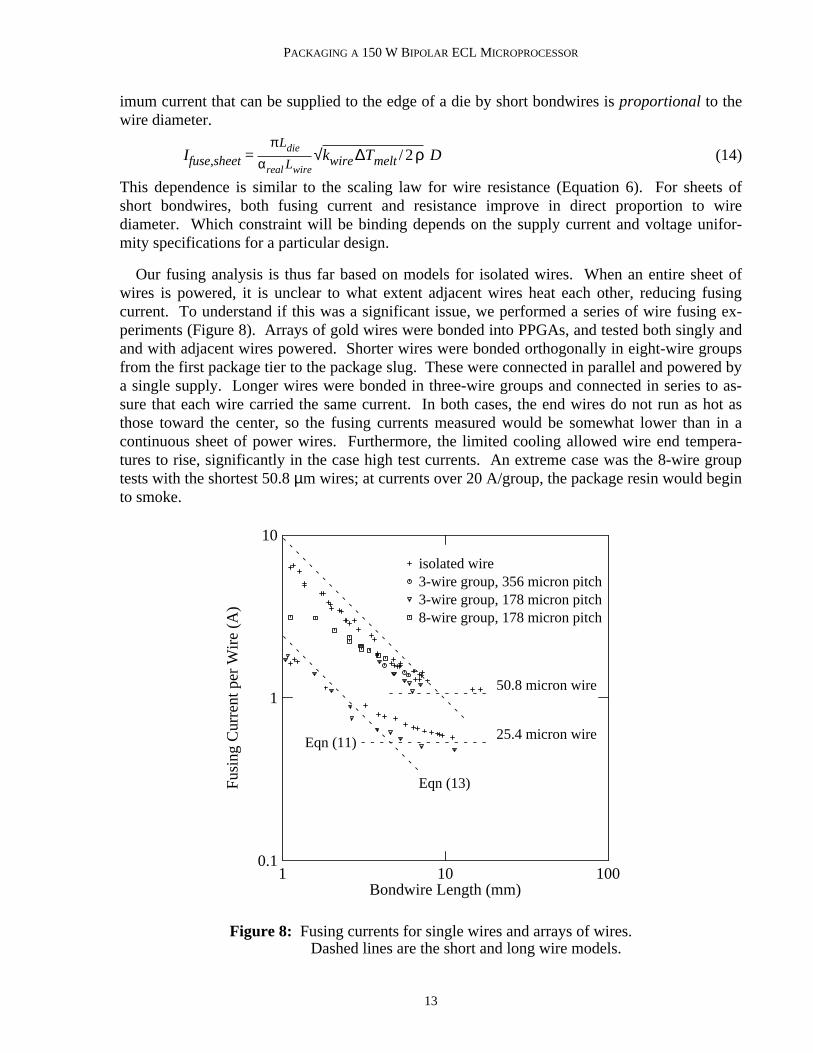
Our fusing analysis is thus far based on models for isolated wires. When an entire sheet ofwires is powered, it is unclear to what extent adjacent wires heat each other, reducing fusingcurrent. To understand if this was a significant issue, we performed a series of wire fusing ex-periments (Figure 8). Arrays of gold wires were bonded into PPGAs, and tested both singly andand with adjacent wires powered. Shorter wires were bonded orthogonally in eight-wire groupsfrom the first package tier to the package slug. These were connected in parallel and powered bya single supply. Longer wires were bonded in three-wire groups and connected in series to as-sure that each wire carried the same current. In both cases, the end wires do not run as hot asthose toward the center, so the fusing currents measured would be somewhat lower than in acontinuous sheet of power wires. Furthermore, the limited cooling allowed wire end tempera-tures to rise, significantly in the case high test currents. An extreme case was the 8-wire grouptests with the shortest 50.8 µm wires; at currents over 20 A/group, the package resin would beginto smoke.
1 10010Bondwire Length (mm)
0.1
10
1
Fusi
ng C
urre
nt p
er W
ire
(A)
isolated wire3-wire group, 356 micron pitch3-wire group, 178 micron pitch8-wire group, 178 micron pitch
Eqn (11)
Eqn (13)
50.8 micron wire
25.4 micron wire
Figure 8: Fusing currents for single wires and arrays of wires.Dashed lines are the short and long wire models.
13
PACKAGING A 150 W BIPOLAR ECL MICROPROCESSOR
As the dashed lines in Figure 8 show, test data from long isolated wires was in good agree-ment with Equation 11. The short isolated wires fused at about 75% of the current predicted bythe Equation 13. This suggests that the wire ends were reaching temperatures higher than the100° C that we had assumed.
Our data shows that heating by adjacent wires is of little importance for the shortest wires, butreduces fusing current by up to 30% in the transition to the long wire regime.
The remaining question is the selection of a fusing current safety factor. For gold bondwiresenveloped by organic encapsulants, the encapsulant’s thermal expansion and decompositioncharacteristics affect the value chosen [8]. But for our free-standing gold wires, the choice isless obvious.
During our testing, we made several observations relevant to the choice of a safety factor. Aslight reddish glow could be seen on gold wires just below the fusing current. A wire could beoperated for hours at this current level without any apparent change, but would blow instantlywhen the current was increased. This suggests that the sort of thermally activated failuremechanisms that are important in aluminum, are less so in gold. Gold has no native oxides, so aslong as physical loads are modest, and there is no interdiffusion of other species, gold wires
***might perform quite adequately at just below the melting point. It has been shown that athigh temperatures, gold wires anneal or recrystalize, and grains grow to form a characteristic‘‘bamboo’’ structure, with grain sizes larger than the wire diameter [9]. While this leads to lowstrength and high elongation limits, and causes early failure in molded packages, it is unclearwhether such microstructural changes preclude safe, high temperature operation for a wire con-strained only at its ends.
Under 40× magnification, bondwires jumped visibly due to thermal expansion when suddenlypowered to 1/3 of their fusing current. This was observed for a wide range of wire lengths.Staying below this threshold assures that wires will not move as current is applied, possiblycausing shorts. While this 3× safety factor is not a particularly satisfying criteria, in the absenceof other data, we chose it for specifying the maximum design current. Clearly, further work isneeded to understand and quantify the risks of operating free-standing gold wires at high tem-peratures and currents.
***As an extreme example, fusing wires would occasionally repair themselves! As we approached the fusingcurrent, stepping up the current in small increments, a wire would repeatedly collapse, shorten, and resolidify,forming a callus at the break site.
14

PACKAGING A 150 W BIPOLAR ECL MICROPROCESSOR
As a final check of our fusing current models, we took a ‘‘mock’’ die created during our diemetalization evaluations, and wirebonded it into our PPGA. The measured diameter of thepower wires was 47 µm. The V wires - the longer power wires - measured 3.0 mm long.eeFigure 8 shows that at this wire length and our 178 µm pitch, adjacent wire heating effects arenegligible. Using Equation 13, we predicted that the eighty V wires would fuse at 224 A.ee
The predicted total current capacity was verified by shorting the on-chip busbars together witha silver-filled epoxy and supplying current to the package pins through a socket. External cool-ing kept the die under 150° C. The V bondwires failed at 164 A, noticeably scorching theeepackage in the neighborhood of the bondfingers. This current was 73% of the value predicted byEquation 13, and in good agreement with our earlier fusing experiments. Since a 150 W dierequires only 29 A @ 5.2 V, it would appear that our margins are ample and wires have reservecapacity for non-uniform power demands.
15
PACKAGING A 150 W BIPOLAR ECL MICROPROCESSOR
3.4. Signal Bondwires
Our bondwire analysis has thus far assumed that the long sides of the die were used entirelyfor supplying power to the die core, relegating all the signal leads to the two short ends of thedie. This is not enough for I/O-hungry microprocessors. A second row of pads is needed aroundthe entire edge of the die. While putting the power pads in the outer row might appear attractive,owing to the shorter resultant bondwires, doing so would demand necking the busbars down tofit between the inner row signal pads. The large spaces required for gold busbar plating wouldlead to a layout that is little denser than a single row. To avoid this, we put the busbar bondpadsand their 162 power wires on the inner row. The 348 signals and 108 I/O reference wires oc-cupied the entire outer row plus the inner row on the narrow ends of the die (Figure 3). Theinner row had a 177.8 µm pitch to accommodate large power wires; by Equation 4, we’d expectto be able to bond at least 46 µm diameter wires on this pitch. The outer row had a 152.4 µmpitch, generous considering we planned to use 33 µm wire. By Equation 4, we’d expect to beable to bond at least 40 µm diameter wires on this pitch.
The wires were bonded in two completely separate arrays. Outer row wires went only to thefirst package tier and inner row wires went only to the second tier. Bondwires did not cross fromouter row on die to second tier on package, and vice versa. This simplified inspection and repairafter the first tier had been bonded. Provided there is sufficient control of wire looping, ourmethodology also allowed the pitches of the two rows to be completely independent. Figure 9shows how the clearance between the rows of bondwires allowed for package tier mis-registration and for arbitrary bondpad pitch on the die. While the two pitches are independent,choosing an appropriate ratio between them simplifies routing die signals to the outer row ofpads.
Between the outer pad row and the scribe street, we provide terminating resistors for the 203input signals. This is the lowest power-density portion of die.
Wafer probing strategy depends on bondpad layout. It would be very difficult to place a probetip on every pad in both rows during wafer testing. Instead we probe only a single row aroundeach diesite: the power connections on the long sides, and half the signals on the ends. Withthese probes, the die could be fully powered, data transferred by use of boundary scan, and thedie exercised with clock and control signals.
16

PACKAGING A 150 W BIPOLAR ECL MICROPROCESSOR
loop-clear
Figure 9: SEM photo showing bondwire loop clearances @100×.
17

PACKAGING A 150 W BIPOLAR ECL MICROPROCESSOR
4. PPGA (Plastic Pin Grid Array)
We chose a plastic package rather than conventional cofired alumina ceramic primarily for thehigh performance of the copper metallization. Plastic pin grid array (PPGA) packaging isgradually gaining acceptance and offers many advantages over conventional ceramic pin gridarray (CPGA) construction [18]. Our 504-pin PPGA is built from copper-clad bizmaliamide-triazine (BT) laminates, plated with soft gold to facilitate wirebonding, and pinned in a 25 x 25array on a 100 mil grid to fit a standard ZIF (zero insertion force) socket. The BT’s 175° C glasstransition temperature makes it possible to wirebond at the high temperatures which are impor-tant for good gold-to-gold bonds. This all-gold interconnect system - die pad, bondwire,bondfinger and pin - is advantageous from a galvanic corrosion viewpoint.
While alumina CPGAs are strong and provide a hermetic environmental seal, PPGAs offerseveral advantages over ceramic:
• Smaller bond pad pitch - PPGAs offer fine patterning; 50 µm minimum lines andspaces are permitted in the package bondpad (bondfinger) area, so a PPGA can ac-commodate as many wires in two tiers as a CPGA can in four. This means shorterwires and a more robust bonding process. While CPGAs have recently becomeavailable with a thin film signal layer on the outermost tier, this doesn’t help us; thefine pitch is needed on the first tier, which handles the signal bondwires from theouter rows on the die.
• Lower sheet resistance package planes - The sheet resistance of each copperpower plane in our PPGA is about 1 mΩ per square. Ceramic planes are typicallyan order of magnitude higher. While CPGAs offer smaller via obstructions and alow incremental cost for adding supplemental planes, it is difficult to overcome thelimitations of the high-resistivity refractory metal conductors.
• Wrap-around die cavity plating - Each layer pair in a PPGA can have plated-through holes (PTH) formed prior to lamination. This PTH metal allows wrapping aconnection from one side of a power plane layer pair, around the die cavity wall, tothe other power plane. This creates a low inductance and resistance connectionfrom the bottom plane to the bondfingers, and allows one PPGA tier to replace twoon a CPGA. It also offers a convenient way to distribute the input terminating volt-age (V = -2.0 V) to the first tier.tt
• Compatible with copper slug - Our thermosiphon technology requires that the met-al die attach ‘‘slug’’ at the bottom of the package cavity also function as the ther-mosiphon boiler. Thermal conductivity, thermosiphon sealing and material com-patibility considerations require the boiler to be made of copper. Attaching a copperboiler directly to a CPGA is difficult, and using an intermediate package slug wouldadversely affect cooling.
• Improved signal integrity - The PPGA’s lower dielectric constant and line resis-tance reduces parasitics. In fact, quite unlike CPGAs, the challenge with PPGAs isgetting a low enough line impedance! An etch-after-plating process produces stub-free signal lines. Plate-though-the-pins and electroless plating processes are becom-ing available to offer stub-free lines for CPGAs.
• Lower tooling and part costs - For comparable complexity, PPGAs can be up to anorder of magnitude less expensive than CPGAs to tool, and finished part costs aresubstantially lower as well.
18

PACKAGING A 150 W BIPOLAR ECL MICROPROCESSOR
For maximum fusing current, the PPGA cavity must be laid out to keep the power bondwiresshort. Minimizing bondwire length requires careful attention to process limitations andcapabilities: clearances, tolerances, and so on. Unfortunately, there are no big terms to engineerinto insignificance, each of many small ones must be painstakingly minimized.
Even with fine patterning of the PPGA metal, laying out the bondfingers for orthogonal bond-ing (having the same pad pitch on package and die) was difficult. This was particularly true forthe 152.4 µm pitch pad on the outer row of the die. Radial bonding (having a larger pitch on thepackage than on the die) would not have helped much due to the shortness of our bondwires andthe size of the die [12]. Instead, we staggered the bondfingers on the package. While this madethe first package tier wider, we felt that the benefit of adequate bondfinger width outweighed theliability of lengthening the bondwires to the second tier. Radial bonding on the second tier wasrejected since varying power wire lengths would have caused varying fusing currents and in-creased voltage variations on the die.
Pads for adhesive bonding 504-size decoupling capacitors were provided on the second bondtier immediately adjacent the bondwires, for the lowest possible series inductance (Figure 3).We also provided mounting holes at the edge of the package for subminiature microwave con-necters for diagnostic signals.
The 156 power pins are dispersed evenly through the pin field, both to spread their heat intothe motherboard, and to improve signal integrity. There are 83 V (ground) pins, 61 V pinscc eeand 12 V (terminating voltage) pins. The V pins are most heavily loaded, but with a 30 Att eesupply, each pin averages only 0.49 A. At these high current levels, however, the motherboardmust feed power symmetrically to the pin field to ensure uniform voltages across the die.
19
PACKAGING A 150 W BIPOLAR ECL MICROPROCESSOR
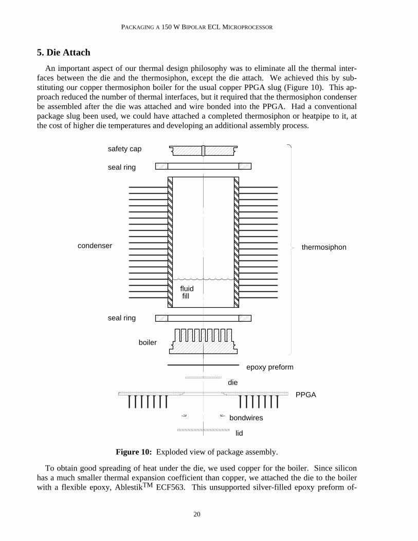
5. Die Attach
An important aspect of our thermal design philosophy was to eliminate all the thermal inter-faces between the die and the thermosiphon, except the die attach. We achieved this by sub-stituting our copper thermosiphon boiler for the usual copper PPGA slug (Figure 10). This ap-proach reduced the number of thermal interfaces, but it required that the thermosiphon condenserbe assembled after the die was attached and wire bonded into the PPGA. Had a conventionalpackage slug been used, we could have attached a completed thermosiphon or heatpipe to it, atthe cost of higher die temperatures and developing an additional assembly process.
fluid fill
seal ring
seal ring
PPGA
die
condenser thermosiphon
lid
bondwires
boiler
epoxy preform
safety cap
Figure 10: Exploded view of package assembly.
To obtain good spreading of heat under the die, we used copper for the boiler. Since siliconhas a much smaller thermal expansion coefficient than copper, we attached the die to the boiler
TMwith a flexible epoxy, Ablestik ECF563. This unsupported silver-filled epoxy preform of-
20

PACKAGING A 150 W BIPOLAR ECL MICROPROCESSOR
fered high thermal conductivity, a low elastic modulus and adequate adhesion. Using preformseliminated the need to develop paste dispensing programs. The bondline could be easily con-trolled by varying the pressure applied during cure. Final bondlines were typically 10 to 20%less than the original 75 µm preform thickness. Acoustic and infrared studies of the epoxy jointindicated void- and delamination-free joints after repeated liquid thermal shocks from -65° C to150° C [6]. At an estimated 1.9 W/m-K, the epoxy thermal conductivity was high enough tokeep the die attach thermal resistance below 0.15° C/W.
Since the epoxy was electrically conductive, the entire thermosiphon was connected to thesame -5.2 volt DC potential as the backside of the ECL die. The thermosiphon would have to becovered by a plastic shroud to protect service personnel. Dielectric materials, such as ceramics,were considered for the boiler or for isolation layers on the boiler / epoxy interface. This wouldallow the condenser to be grounded, but at the cost of higher die operating temperatures.
The die and PPGA were simultaneously bonded to the boiler, using a single epoxy preformand bonding fixture (see Figure 10). The following die attach process was used:
• Electroless nickel plated boiler placed in fixture with flat side facing upward.
• Epoxy preform placed on boiler.
• PPGA placed onto fixture locating features and lowered onto epoxy.
• Die placed in cavity on exposed epoxy, located by tabs that are part of the PPGA.
• Pressure distribution pad placed on die.
• Spring mechanism pressed on pad, squeezing die into epoxy. A second springpressed PPGA into epoxy.
• Fixtured assembly heated to 130° C for two hours.
To distribute the pressure evenly across the large die, we used an elastomer pad with aTMKapton polyimide film backing. This pad was bonded to a steel backing plate that was
guided by two of the PPGA pins. This accurately located the pad to the die. A springmechanism pushed on this backing plate through a steel ball bonded to the exact center of theplate. The ball assured that during cure, the load remained accurately centered and perpendicularto the die. By changing springs, the pressure on either the die or the PPGA-to-boiler joint couldbe independently adjusted about the 400 kPa nominal value. Under these high cure pressures,the locating tabs in the PPGA cavity proved important in preventing the die from squirming outof position.
The Kapton polyimide layer ensured that the gold bond pads on the die would not be con-taminated during die attach. Several metal foils were also evaluated for this purpose; all marredthe die surface to some extent. Based on surface examination with laser microprobe massspectrometry (LIMS), tantalum and Kapton did not transfer contaminants to the gold during asimulated curing cycle. The Ni foil was marginal, and Ti, Co, V, and W all substantially con-taminated the gold. Kapton was selected for its low cost and ease of handling.
A temperature controller and cartridge heaters in the bonding fixture brought the assembly tothe desired cure temperature. To reduce oxidation and void formation, we experimented withmaintaining a vacuum on the fixture as the epoxy heated and began to flow. This proved un-necessary since atmospheric cure conditions gave reliable and void-free bonds.
21
PACKAGING A 150 W BIPOLAR ECL MICROPROCESSOR
6. Thermosiphon Cooling
A thermosiphon is a phase-change heatsink consisting of a sealed vessel containing a volatileliquid. When heat is supplied to the bottom end - the boiler or evaporator - the liquid vaporizesand moves to the cooled portion - the condenser. There it condenses, giving up its energy to theair passing over the external fins. The condensate then returns to the heated end where it repeatsthe cycle (Figure 10). A thermosiphon is essentially a wickless heatpipe [13]. It relies ongravity, rather than the capillary forces of a wick, to return condensate to the boiler. The wickcan limit the performance of a heatpipe [2]. We chose a thermosiphon instead of a heatpipebecause of its simplicity and the large heat fluxes it could handle. We used a mercury tip switchto interrupt power to prevent overheating should the thermosiphon inadvertently be tipped upsidedown. A thermosiphon is more expensive than a solid metal heatsink, but in VLSI packagingapplications it becomes attractive when die power exceeds 50 to 100 W. At these power levels, asolid heatsink would have to be very large and would require significant air flow. Because it hasno apparent moving parts, the casual observer views the thermosiphon as nothing more than anefficient air-cooled heatsink.
We built our thermosiphon by combining the package boiler with spirally finned coppertubing as the condenser. The nickel-plated copper boiler that holds the die had fins cut into oneside for the boiling surface of the thermosiphon. The fin geometry was chosen after boilingstudies of water at subatmospheric pressures [15]. We built condensers of 2.85 cm diametercopper tubing with two types of fins. Copper fins spirally wrapped and brazed onto the tubeprovided the best thermal performance, while tension-wrapped aluminum fins provided thelightest condenser. All fins had an outside diameter of 5.4 cm and a pitch of 4 fins per cm. Thecondenser was 12 cm long to accommodate two adjacent 60 mm diameter fans and to allow theassembly to fit inside a standard desk-top box. The two fans, in parallel, quietly supplied 7liters/s (≈17 c.f.m.) of air at a static pressure drop of 18 Pa (0.07 inches of H O).2
A safety cap plugged the condenser end of the thermosiphon. This nickel-plated copper caphad a hole drilled through it which was plugged with a low temperature solder. Should thethermosiphon be exposed to a fire or some other high temperature fault condition, the solderwould melt and release the internal pressure before vessel rupture.
The choice of operating fluid significantly affects thermosiphon performance. Water is adesirable working fluid for a thermosiphon since it has such a high heat of vaporization, highthermal conductivity, and is nontoxic and nonflammable. However, from our earlier studies, wefound that at subatmospheric pressures and at our heat fluxes, the boiling behavior of water be-came sporadic. [16] By adding a small amount of alcohol to the water, the surface tension andthermodynamic conditions changed significantly enough to provide steady boiling. In fact, atcertain mixture ratios, the critical heat flux could be improved above that of pure water by 100%![17] A mixture of 22% propanol in water, by volume, was chosen for our thermosiphon becauseof performance characteristics, its non-toxicity and because at this concentration, the U.S.Department of Transportation does not classify it as a flammable or combustible liquid.
Cleanliness of assembled parts was essential because non-condensable gases and other con-taminants degrade the performance of a thermosiphon. Scale on the hot regions of the ther-mosiphon could hinder boiling performance, ionics could cause corrosion, and noncondensablegases could gather in the cooled end, blanketing condenser surface. In order to avoid trapping
22

PACKAGING A 150 W BIPOLAR ECL MICROPROCESSOR
solder fluxes or additional materials in the thermosiphon, an intrinsically clean sealing techniquewas used. The copper tube of the condenser was hermetically sealed onto the boiler and cap by ashape memory ring supplied by Raychem Corp. When electrically heated to 180° C, this nickel-titanium alloy ring shrinks by roughly 5% in diameter. This squeezed the tube onto a smallpositive feature, or sealing land, on the outside diameter of the boiler and cap [3] (Figure 11). A
Figure 11: Section view of the condenser tube sealed on the boilerby the shape memory ring. The land feature is 0.3 mm high.
soft tube material and hard sealing land were essential to achieve a plastically deformed seal withgood land penetration into the tube (Figure 12). A helium leak detector verified that with an-nealed copper tubing and a precipitation-hardened chrome-copper boiler and cap, reliable sealswere obtained, even after twenty -65° C to 150° C thermal shock cycles.
20 7030 40 50 60Tube Hardness (Rockwell 45 T)
0
0.2
0.05
0.1
0.15
0.2
Seal
ing
Lan
d Pe
netr
atio
n (
mm
)
Figure 12: Land penetration into the condenser tube versus tubehardness. This land was made of nickel-plated OFHC copper.
23

PACKAGING A 150 W BIPOLAR ECL MICROPROCESSOR
The following assembly procedure was used for the thermosiphon:
• Boiler, with PPGA and wire-bonded die, attached to condenser using shape memoryring.
• Liquid mixture added to condenser.
• Chip powered to boil and degas liquid. Boiling continues to purge gases from con-denser.
• At desired fill volume (~20%) and desired alcohol-water mixture (22% alcohol byvolume), safety cap sealed in place with a second shape memory ring.
Sealing the condenser while the liquid was boiling ensured a saturated state inside the ther-mosiphon. This minimized the internal operating pressure, and hence operating temperature.
To check cooling system performance, we used a test die with TaN thin-film resistor patternsbetween and underneath the gold busbars. The resistor layer was patterned so that when the testdie was wirebonded into a package, it duplicated the current draw and power dissipation of a livepart. We coated a thin layer of filled silicone to the surface of the die, to increase its emissivityfor infrared temperature measurements. Figure 13 shows the performance of the entire coolingsystem at various die powers and constant air flow. The nonlinear behavior was due to thechanging internal pressure, which caused boiling variations as the heat flux changed. The flatportion of the curve corresponds to steady nucleate boiling. In this power range, thethermosiphon’s thermal resistance, from the boiler to the cooling air, was below 0.32° C/W. Theflat portion of the performance curve in Figure 13 may be shifted significantly by changing thesurface area of the boiler.
0 30050 100 150 200 250Die Power (W)
0
1.2
0.2
0.4
0.6
0.8
1
The
rmal
Res
ista
nce
(C/W
)
Figure 13: Junction-to-air thermal resistance as a function of diepower, with copper-finned condenser and 7 liter/s airflow.
24

PACKAGING A 150 W BIPOLAR ECL MICROPROCESSOR
7. Conclusions
While much work remains to formally qualify this packaging approach, it appears to offer alow-cost solution for powering, cooling, and connecting high wattage microprocessor die. Thenecessary technologies include:
• Thick gold busbars across the surface of the die to uniformly distribute large supplycurrents.
• Two-row, non-staggered ball bonding around the edge of the die, for good signaland power distribution.
• PPGA package with low sheet resistance copper planes for distributing power, andfine patterning capabilities for dense bondfinger pitch.
• Low modulus silver-filled epoxy die attach directly to the copper heatsink.
• Thermosiphon with alcohol-water fill for quiet air-cooling.
Many variations are possible to meet differing requirements, but thick die metal, double-rowwire bonding, a minimum number of thermal interfaces, and phase-change cooling are all essen-tial ingredients.
Future work may include investigating the behavior of gold wires at sustained high current,obtaining die coatings with good adhesion and environmental protection, performing long-termthermosiphon tests, and developing enhancements to handle larger die and higher power levels.
8. Acknowledgements
We wish to acknowledge the vital contribution of Wade R. McGillis, who conducted the fun-damental boiling studies that guided our thermosiphon fluid selection and boiler fin design.Norm Jouppi was our key resource in defining the project and guiding packaging design deci-sions. The authors also wish to thank Betsy Fitch and Mary Jo Doherty for reviewing themanuscript and providing their many critical comments and corrections.
25

PACKAGING A 150 W BIPOLAR ECL MICROPROCESSOR
26
PACKAGING A 150 W BIPOLAR ECL MICROPROCESSOR
References[1] K. A. Awkward and R. D. Lewis.
Model for Determining Thermal Profiles of Bond Wires Using ‘‘PSPICE’’ Analysis.In 7th SEMI-THERM Proceedings 1991, pages 86-90. SEMI-THERM Conference,
Phoenix, Arizona, February, 1991.
[2] B. K. Bage and G. P. Peterson.A Review of Entrainment Limits in Thermosyphons and Heat Pipes.In Porous Media, Mixtures, and Multiphase Heat Transfer. Winter Annual Meeting,
ASME, San Francisco, December, 1989.
[3] T. Borden.Shape Memory Alloys Form a Tight Fit.Mechanical Engineering 113, No. 10:66-72, 1991.
[4] M. Coxon, C. Kershner and D. M. McEligot.Transient Current Capacities of Bond Wires in Hybrid Microcircuits.IEEE Trans. Components, Hybrids, and Manufacturing Technology
CHMT-9(3):279-285, September, 1986.
[5] D. Dobberpuhl et al. (1992).A 200MHz 64 Bit Dual Issue CMOS Microprocessor.In Proceedings of the 1992 International Solid-State Circuits Conference. San Francisco,
California, February, 1992.
[6] J. S. Fitch.A Comparison of Acoustic and Infrared Inspection Techniques for Die Attach.In I-THERM III Proceedings 1992, pages 159-164. I-THERM Conference, Austin,
Texas, February, 1992.
[7] J. L. Hennesey and N. P. Jouppi.Computer Technology and Architecture: An Evolving Interaction.Computer 24(9):18-29, September, 1991.
[8] G. J. Hill, B. C. Roberts and C. P. Strudwick.Safe Operating Limits for Backdriving in ATE.In Proceedings of the 1987 International Test Conference, pages 798-804. IEEE, 1987.
[9] R. Hofbeck, K. Hausmann, B. Ilscher and H. U. Kunzi.Fatigue of Very Thin Copper and Gold Wires.Scripta Metallurgica 20:1601-1605, 1986.
[10] J. P. Holman.Heat Transfer.McGraw-Hill, Washington , 1976 - 4th Ed.ISBN 0-07-029598-0.
[11] J. Schultz.A CMOS 100Mhz Microprocessor.In Proceedings 1991 IEEE International Solid State Circuits Conference, pages 90-91.
IEEE, San Francisco, February, 1991.
27
PACKAGING A 150 W BIPOLAR ECL MICROPROCESSOR
[12] W. E. Jahsman.Lead Frame and Wire Length Limitations to Bond Densification.Journal of Electronic Packaging 111(4):289-293, December, 1989.
[13] A. D. Kraus and A. Bar-Cohen.Thermal Analysis and Control of Electronic Equipment.Hemisphere, Washington , 1983.ISBN 0-07-035416-2.
[14] L. Kohn and S. Fu.A 1,000,000 Transistor Microprocessor.In Proceedings 1989 IEEE International Solid State Circuits Conference, pages 54-55.
IEEE, New York, February, 1989.
[15] W. R. McGillis, V. P. Carey, J. S. Fitch and W. R. Hamburgen.Pool Boiling Enhancement Techniques for Water at Low Pressure.In Proceedings of the Seventh IEEE Semiconductor Thermal Measurement and Manage-
ment Symposium, pages 64-72. 1991 IEEE Semiconductor Thermal Measurementand Management Symposium - SEMI-THERM, Phoenix, Arizona, February, 1991.
[16] W. R. McGillis, V. P. Carey, J. S. Fitch and W. R. Hamburgen.Pool Boiling on Small Dissipating Elements at Subatmospheric Pressure.In Proceedings on Phase Change Heat Transfer, pages 27-36. 1991 ASME National
Heat Transfer Conference, Minneapolis,Minnesota, July, 1991.
[17] W. R. McGillis, J. S. Fitch, V. P. Carey and W. R. Hamburgen.Boiling Binary Mixtures at Subatmospheric Pressure.In I-THERM III Proceedings 1992, pages 127-136. I-THERM Conference, Austin,
Texas, February, 1992.
[18] T. Miwa, K. Otsuka, et al.High Reliability and Low Cost Design in Plastic PGA Package with High Performance.In Proceedings 41st Electronic Components & Technology Conference, pages 183-189.
IEEE, Atlanta, Georgia, May, 1991.
[19] Y. Ohno, et al.Development of Ultra Fine Wire for Fine Pitch Bonding.In Proceedings 41st Electronic Components & Technology Conference, pages 519-523.
IEEE, Atlanta, Georgia, May, 1991.
[20] D. Priore, Digital Equipment Corp., personal communication, September, 1990.September, 1990.
[21] E. M. Savitskii (ed).Handbook of Precious Metals.Hemisphere, New York, 1989.ISBN 0-89116-709-9.
[22] B. Shu.Fine Pitch Wire Bonding Development Using a New Multipurpose, Multi-pad Pitch Test
Die.In Proceedings 41st Electronic Components & Technology Conference, pages 511-518.
IEEE, Atlanta, Georgia, May, 1991.
28

PACKAGING A 150 W BIPOLAR ECL MICROPROCESSOR
[23] D. Tanksalvala, et. al.A 90Mhz CMOS RISC CPU Designed for Sustained Performance.In Proceedings 1990 IEEE International Solid State Circuits Conference, pages 52-53.
IEEE, San Francisco, February, 1990.
29

PACKAGING A 150 W BIPOLAR ECL MICROPROCESSOR
30

PACKAGING A 150 W BIPOLAR ECL MICROPROCESSOR
WRL Research Reports
‘‘Titan System Manual.’’ ‘‘MultiTitan: Four Architecture Papers.’’
Michael J. K. Nielsen. Norman P. Jouppi, Jeremy Dion, David Boggs, Mich-
WRL Research Report 86/1, September 1986. ael J. K. Nielsen.
WRL Research Report 87/8, April 1988.‘‘Global Register Allocation at Link Time.’’
David W. Wall. ‘‘Fast Printed Circuit Board Routing.’’
WRL Research Report 86/3, October 1986. Jeremy Dion.
WRL Research Report 88/1, March 1988.‘‘Optimal Finned Heat Sinks.’’
William R. Hamburgen. ‘‘Compacting Garbage Collection with Ambiguous
WRL Research Report 86/4, October 1986. Roots.’’
Joel F. Bartlett.‘‘The Mahler Experience: Using an Intermediate WRL Research Report 88/2, February 1988.
Language as the Machine Description.’’
David W. Wall and Michael L. Powell. ‘‘The Experimental Literature of The Internet: An
WRL Research Report 87/1, August 1987. Annotated Bibliography.’’
Jeffrey C. Mogul.‘‘The Packet Filter: An Efficient Mechanism for WRL Research Report 88/3, August 1988.
User-level Network Code.’’
Jeffrey C. Mogul, Richard F. Rashid, Michael ‘‘Measured Capacity of an Ethernet: Myths and
J. Accetta. Reality.’’
WRL Research Report 87/2, November 1987. David R. Boggs, Jeffrey C. Mogul, Christopher
A. Kent.‘‘Fragmentation Considered Harmful.’’ WRL Research Report 88/4, September 1988.Christopher A. Kent, Jeffrey C. Mogul.
WRL Research Report 87/3, December 1987. ‘‘Visa Protocols for Controlling Inter-Organizational
Datagram Flow: Extended Description.’’‘‘Cache Coherence in Distributed Systems.’’ Deborah Estrin, Jeffrey C. Mogul, Gene Tsudik,Christopher A. Kent. Kamaljit Anand.WRL Research Report 87/4, December 1987. WRL Research Report 88/5, December 1988.
‘‘Register Windows vs. Register Allocation.’’ ‘‘SCHEME->C A Portable Scheme-to-C Compiler.’’David W. Wall. Joel F. Bartlett.WRL Research Report 87/5, December 1987. WRL Research Report 89/1, January 1989.
‘‘Editing Graphical Objects Using Procedural ‘‘Optimal Group Distribution in Carry-Skip Ad-Representations.’’ ders.’’
Paul J. Asente. Silvio Turrini.WRL Research Report 87/6, November 1987. WRL Research Report 89/2, February 1989.
‘‘The USENET Cookbook: an Experiment in ‘‘Precise Robotic Paste Dot Dispensing.’’Electronic Publication.’’ William R. Hamburgen.
Brian K. Reid. WRL Research Report 89/3, February 1989.WRL Research Report 87/7, December 1987.
31
PACKAGING A 150 W BIPOLAR ECL MICROPROCESSOR
‘‘Simple and Flexible Datagram Access Controls for ‘‘Link-Time Code Modification.’’
Unix-based Gateways.’’ David W. Wall.
Jeffrey C. Mogul. WRL Research Report 89/17, September 1989.
WRL Research Report 89/4, March 1989.‘‘Noise Issues in the ECL Circuit Family.’’
Jeffrey Y.F. Tang and J. Leon Yang.‘‘Spritely NFS: Implementation and Performance ofWRL Research Report 90/1, January 1990.Cache-Consistency Protocols.’’
V. Srinivasan and Jeffrey C. Mogul.‘‘Efficient Generation of Test Patterns UsingWRL Research Report 89/5, May 1989.
Boolean Satisfiablilty.’’
Tracy Larrabee.‘‘Available Instruction-Level Parallelism for Super-WRL Research Report 90/2, February 1990.scalar and Superpipelined Machines.’’
Norman P. Jouppi and David W. Wall.‘‘Two Papers on Test Pattern Generation.’’WRL Research Report 89/7, July 1989.Tracy Larrabee.
WRL Research Report 90/3, March 1990.‘‘A Unified Vector/Scalar Floating-Point Architec-
ture.’’‘‘Virtual Memory vs. The File System.’’Norman P. Jouppi, Jonathan Bertoni, and DavidMichael N. Nelson.W. Wall.WRL Research Report 90/4, March 1990.WRL Research Report 89/8, July 1989.
‘‘Efficient Use of Workstations for Passive Monitor-‘‘Architectural and Organizational Tradeoffs in theing of Local Area Networks.’’Design of the MultiTitan CPU.’’
Jeffrey C. Mogul.Norman P. Jouppi.WRL Research Report 90/5, July 1990.WRL Research Report 89/9, July 1989.
‘‘A One-Dimensional Thermal Model for the VAX‘‘Integration and Packaging Plateaus of Processor9000 Multi Chip Units.’’Performance.’’
John S. Fitch.Norman P. Jouppi.WRL Research Report 90/6, July 1990.WRL Research Report 89/10, July 1989.
‘‘1990 DECWRL/Livermore Magic Release.’’‘‘A 20-MIPS Sustained 32-bit CMOS Microproces-Robert N. Mayo, Michael H. Arnold, Walter S. Scott,sor with High Ratio of Sustained to Peak Perfor-
Don Stark, Gordon T. Hamachi.mance.’’WRL Research Report 90/7, September 1990.Norman P. Jouppi and Jeffrey Y. F. Tang.
WRL Research Report 89/11, July 1989.‘‘Pool Boiling Enhancement Techniques for Water at
Low Pressure.’’‘‘The Distribution of Instruction-Level and MachineWade R. McGillis, John S. Fitch, WilliamParallelism and Its Effect on Performance.’’
R. Hamburgen, Van P. Carey.Norman P. Jouppi.WRL Research Report 90/9, December 1990.WRL Research Report 89/13, July 1989.
‘‘Writing Fast X Servers for Dumb Color Frame Buf-‘‘Long Address Traces from RISC Machines:fers.’’Generation and Analysis.’’
Joel McCormack.Anita Borg, R.E.Kessler, Georgia Lazana, and DavidWRL Research Report 91/1, February 1991.W. Wall.
WRL Research Report 89/14, September 1989.
32

PACKAGING A 150 W BIPOLAR ECL MICROPROCESSOR
‘‘A Simulation Based Study of TLB Performance.’’ ‘‘Packaging a 150 W Bipolar ECL Microprocessor.’’
J. Bradley Chen, Anita Borg, Norman P. Jouppi. William R. Hamburgen, John S. Fitch,.
WRL Research Report 91/2, November 1991. WRL Research Report 92/1, March 1992.
‘‘Analysis of Power Supply Networks in VLSI Cir-
cuits.’’
Don Stark.
WRL Research Report 91/3, April 1991.
‘‘TurboChannel T1 Adapter.’’
David Boggs.
WRL Research Report 91/4, April 1991.
‘‘Procedure Merging with Instruction Caches.’’
Scott McFarling.
WRL Research Report 91/5, March 1991.
‘‘Don’t Fidget with Widgets, Draw!.’’
Joel Bartlett.
WRL Research Report 91/6, May 1991.
‘‘Pool Boiling on Small Heat Dissipating Elements in
Water at Subatmospheric Pressure.’’
Wade R. McGillis, John S. Fitch, William
R. Hamburgen, Van P. Carey.
WRL Research Report 91/7, June 1991.
‘‘Incremental, Generational Mostly-Copying Gar-
bage Collection in Uncooperative Environ-
ments.’’
G. May Yip.
WRL Research Report 91/8, June 1991.
‘‘Interleaved Fin Thermal Connectors for Multichip
Modules.’’
William R. Hamburgen.WRL Research Report 91/9, August 1991.
‘‘Experience with a Software-defined Machine Ar-
chitecture.’’
David W. Wall.
WRL Research Report 91/10, August 1991.
‘‘Network Locality at the Scale of Processes.’’
Jeffrey C. Mogul.
WRL Research Report 91/11, November 1991.
33

PACKAGING A 150 W BIPOLAR ECL MICROPROCESSOR
WRL Technical Notes
‘‘TCP/IP PrintServer: Print Server Protocol.’’ ‘‘Systems for Late Code Modification.’’
Brian K. Reid and Christopher A. Kent. David W. Wall.
WRL Technical Note TN-4, September 1988. WRL Technical Note TN-19, June 1991.
‘‘TCP/IP PrintServer: Server Architecture and Im- ‘‘Unreachable Procedures in Object-oriented Pro-
plementation.’’ gramming.’’
Christopher A. Kent. Amitabh Srivastava.
WRL Technical Note TN-7, November 1988. WRL Technical Note TN-21, November 1991.
‘‘Smart Code, Stupid Memory: A Fast X Server for a ‘‘Cache Replacement with Dynamic Exclusion’’
Dumb Color Frame Buffer.’’ Scott McFarling.
Joel McCormack. WRL Technical Note TN-22, November 1991.
WRL Technical Note TN-9, September 1989.‘‘Boiling Binary Mixtures at Subatmospheric Pres-
‘‘Why Aren’t Operating Systems Getting Faster As sures’’
Fast As Hardware?’’ Wade R. McGillis, John S. Fitch, William
John Ousterhout. R. Hamburgen, Van P. Carey.
WRL Technical Note TN-11, October 1989. WRL Technical Note TN-23, January 1992.
‘‘Mostly-Copying Garbage Collection Picks Up ‘‘A Comparison of Acoustic and Infrared Inspection
Generations and C++.’’ Techniques for Die Attach’’
Joel F. Bartlett. John S. Fitch.
WRL Technical Note TN-12, October 1989. WRL Technical Note TN-24, January 1992.
‘‘Limits of Instruction-Level Parallelism.’’
David W. Wall.
WRL Technical Note TN-15, December 1990.
‘‘The Effect of Context Switches on Cache Perfor-
mance.’’
Jeffrey C. Mogul and Anita Borg.WRL Technical Note TN-16, December 1990.
‘‘MTOOL: A Method For Detecting Memory Bot-
tlenecks.’’
Aaron Goldberg and John Hennessy.
WRL Technical Note TN-17, December 1990.
‘‘Predicting Program Behavior Using Real or Es-
timated Profiles.’’
David W. Wall.WRL Technical Note TN-18, December 1990.
34