P6800 Series Logic Analyzer Probes Instruction Manualdownload.tek.com/manual/077014102web.pdf ·...
89
xx P6800 Series Logic Analyzer Probes ZZZ Instruction Manual *P077014102* 077-0141-02
Transcript of P6800 Series Logic Analyzer Probes Instruction Manualdownload.tek.com/manual/077014102web.pdf ·...

xx
P6800 SeriesLogic Analyzer Probes
ZZZ
Instruction Manual
*P077014102*
077-0141-02


P6800 SeriesLogic Analyzer Probes
ZZZ
Instruction Manual
xx
www.tektronix.com077-0141-02

Copyright © Tektronix. All rights reserved. Licensed software products are owned by Tektronix or its subsidiariesor suppliers, and are protected by national copyright laws and international treaty provisions.
Tektronix products are covered by U.S. and foreign patents, issued and pending. Information in this publicationsupersedes that in all previously published material. Specifications and price change privileges reserved.
TEKTRONIX and TEK are registered trademarks of Tektronix, Inc.
MagniVu, iView, PatGenVu, PowerFlex, QuickStart, and TLAVu are unregistered trademarks of Tektronix, Inc.
Contacting Tektronix
Tektronix, Inc.14200 SW Karl Braun DriveP.O. Box 500Beaverton, OR 97077USA
For product information, sales, service, and technical support:In North America, call 1-800-833-9200.Worldwide, visit www.tektronix.com to find contacts in your area.

Warranty
Tektronix warrants that this product will be free from defects in materials and workmanship for a period of one (1)year from the date of shipment. If any such product proves defective during this warranty period, Tektronix, at itsoption, either will repair the defective product without charge for parts and labor, or will provide a replacementin exchange for the defective product. Parts, modules and replacement products used by Tektronix for warrantywork may be new or reconditioned to like new performance. All replaced parts, modules and products becomethe property of Tektronix.
In order to obtain service under this warranty, Customer must notify Tektronix of the defect before the expiration ofthe warranty period and make suitable arrangements for the performance of service. Customer shall be responsiblefor packaging and shipping the defective product to the service center designated by Tektronix, with shippingcharges prepaid. Tektronix shall pay for the return of the product to Customer if the shipment is to a location withinthe country in which the Tektronix service center is located. Customer shall be responsible for paying all shippingcharges, duties, taxes, and any other charges for products returned to any other locations.
This warranty shall not apply to any defect, failure or damage caused by improper use or improper or inadequatemaintenance and care. Tektronix shall not be obligated to furnish service under this warranty a) to repair damageresulting from attempts by personnel other than Tektronix representatives to install, repair or service the product;b) to repair damage resulting from improper use or connection to incompatible equipment; c) to repair any damageor malfunction caused by the use of non-Tektronix supplies; or d) to service a product that has been modified orintegrated with other products when the effect of such modification or integration increases the time or difficultyof servicing the product.
THIS WARRANTY IS GIVEN BY TEKTRONIX WITH RESPECT TO THE PRODUCT IN LIEU OF ANYOTHER WARRANTIES, EXPRESS OR IMPLIED. TEKTRONIX AND ITS VENDORS DISCLAIM ANYIMPLIED WARRANTIES OF MERCHANTABILITY OR FITNESS FOR A PARTICULAR PURPOSE.TEKTRONIX’ RESPONSIBILITY TO REPAIR OR REPLACE DEFECTIVE PRODUCTS IS THE SOLEAND EXCLUSIVE REMEDY PROVIDED TO THE CUSTOMER FOR BREACH OF THIS WARRANTY.TEKTRONIX AND ITS VENDORS WILL NOT BE LIABLE FOR ANY INDIRECT, SPECIAL, INCIDENTAL,OR CONSEQUENTIAL DAMAGES IRRESPECTIVE OF WHETHER TEKTRONIX OR THE VENDOR HASADVANCE NOTICE OF THE POSSIBILITY OF SUCH DAMAGES.
[W2 – 15AUG04]


Table of Contents
Preface .. . . . . . . . . . . . . . . . . . . . . . . . . . . . . . . . . . . . . . . . . . . . . . . . . . . . . . . . . . . . . . . . . . . . . . . . . . . . . . . . . . . . . . . . . . . . . . . . . . . . . . . . . . . . . . vRelated Documentation .. . . . . . . . . . . . . . . . . . . . . . . . . . . . . . . . . . . . . . . . . . . . . . . . . . . . . . . . . . . . . . . . . . . . . . . . . . . . . . . . . . . . . . vCommonly Used Terms .. . . . . . . . . . . . . . . . . . . . . . . . . . . . . . . . . . . . . . . . . . . . . . . . . . . . . . . . . . . . . . . . . . . . . . . . . . . . . . . . . . . . . vi
Operating Basics. . . . . . . . . . . . . . . . . . . . . . . . . . . . . . . . . . . . . . . . . . . . . . . . . . . . . . . . . . . . . . . . . . . . . . . . . . . . . . . . . . . . . . . . . . . . . . . . . . . . 1Product Description. . . . . . . . . . . . . . . . . . . . . . . . . . . . . . . . . . . . . . . . . . . . . . . . . . . . . . . . . . . . . . . . . . . . . . . . . . . . . . . . . . . . . . . . . . . . 1
P6810 General Purpose Probe .. . . . . . . . . . . . . . . . . . . . . . . . . . . . . . . . . . . . . . . . . . . . . . . . . . . . . . . . . . . . . . . . . . . . . . . . . . 2P6810 Leadset Adapters and Accessories . . . . . . . . . . . . . . . . . . . . . . . . . . . . . . . . . . . . . . . . . . . . . . . . . . . . . . . . . . . . . . 3P6860 High-Density Probe . . . . . . . . . . . . . . . . . . . . . . . . . . . . . . . . . . . . . . . . . . . . . . . . . . . . . . . . . . . . . . . . . . . . . . . . . . . . . . 5P6864 High-Density 4X Probe . . . . . . . . . . . . . . . . . . . . . . . . . . . . . . . . . . . . . . . . . . . . . . . . . . . . . . . . . . . . . . . . . . . . . . . . . . 6P6880 High-Density Differential Probe . . . . . . . . . . . . . . . . . . . . . . . . . . . . . . . . . . . . . . . . . . . . . . . . . . . . . . . . . . . . . . . . 7Mictor-on-PCB to P6860 Compression Adapter . . . . . . . . . . . . . . . . . . . . . . . . . . . . . . . . . . . . . . . . . . . . . . . . . . . . . . 8Compression-on-PCB to P6434 Mictor Adapter . . . . . . . . . . . . . . . . . . . . . . . . . . . . . . . . . . . . . . . . . . . . . . . . . . . . . 10
Attaching Probe Labels . . . . . . . . . . . . . . . . . . . . . . . . . . . . . . . . . . . . . . . . . . . . . . . . . . . . . . . . . . . . . . . . . . . . . . . . . . . . . . . . . . . . . . 12Connecting the Probes to the Logic Analyzer . . . . . . . . . . . . . . . . . . . . . . . . . . . . . . . . . . . . . . . . . . . . . . . . . . . . . . . . . . . . . 12Cleaning the P686x and P6880 Compression Footprints. . . . . . . . . . . . . . . . . . . . . . . . . . . . . . . . . . . . . . . . . . . . . . . . . 13Cleaning the P686x and P6880 Probe Heads .. . . . . . . . . . . . . . . . . . . . . . . . . . . . . . . . . . . . . . . . . . . . . . . . . . . . . . . . . . . . . 14Storing the P686x and P6880 Probe Heads .. . . . . . . . . . . . . . . . . . . . . . . . . . . . . . . . . . . . . . . . . . . . . . . . . . . . . . . . . . . . . . . 15Connecting the Probes to the Target System.. . . . . . . . . . . . . . . . . . . . . . . . . . . . . . . . . . . . . . . . . . . . . . . . . . . . . . . . . . . . . . 16
Connecting the P6810 General Purpose Probe . . . . . . . . . . . . . . . . . . . . . . . . . . . . . . . . . . . . . . . . . . . . . . . . . . . . . . . 16Connecting the P686x High Density and P6880 Differential Probes . . . . . . . . . . . . . . . . . . . . . . . . . . . . . . 18Connecting the Mictor-on-PCB to P6860 Compression Adapter (Applies to P6860 Probe
Only). . . . . . . . . . . . . . . . . . . . . . . . . . . . . . . . . . . . . . . . . . . . . . . . . . . . . . . . . . . . . . . . . . . . . . . . . . . . . . . . . . . . . . . . . . . . . . . . . . 21Connecting the Compression-on-PCB to P6434 Mictor Adapter. . . . . . . . . . . . . . . . . . . . . . . . . . . . . . . . . . . 21
Reference . . . . . . . . . . . . . . . . . . . . . . . . . . . . . . . . . . . . . . . . . . . . . . . . . . . . . . . . . . . . . . . . . . . . . . . . . . . . . . . . . . . . . . . . . . . . . . . . . . . . . . . . . . . 23Designing an Interface Between the P6800 Probes and a Target System.. . . . . . . . . . . . . . . . . . . . . . . . . . . . . . 23
Signal Fixturing Considerations. . . . . . . . . . . . . . . . . . . . . . . . . . . . . . . . . . . . . . . . . . . . . . . . . . . . . . . . . . . . . . . . . . . . . . . . 23Signal Names . . . . . . . . . . . . . . . . . . . . . . . . . . . . . . . . . . . . . . . . . . . . . . . . . . . . . . . . . . . . . . . . . . . . . . . . . . . . . . . . . . . . . . . . . . . . . 28Land Footprints . . . . . . . . . . . . . . . . . . . . . . . . . . . . . . . . . . . . . . . . . . . . . . . . . . . . . . . . . . . . . . . . . . . . . . . . . . . . . . . . . . . . . . . . . . 44Mechanical Considerations . . . . . . . . . . . . . . . . . . . . . . . . . . . . . . . . . . . . . . . . . . . . . . . . . . . . . . . . . . . . . . . . . . . . . . . . . . . . . 48Electrical Considerations. . . . . . . . . . . . . . . . . . . . . . . . . . . . . . . . . . . . . . . . . . . . . . . . . . . . . . . . . . . . . . . . . . . . . . . . . . . . . . . . 55
Specifications . . . . . . . . . . . . . . . . . . . . . . . . . . . . . . . . . . . . . . . . . . . . . . . . . . . . . . . . . . . . . . . . . . . . . . . . . . . . . . . . . . . . . . . . . . . . . . . . . . . . . . 61Mechanical and Electrical Specifications . . . . . . . . . . . . . . . . . . . . . . . . . . . . . . . . . . . . . . . . . . . . . . . . . . . . . . . . . . . . . . . . . . 61
Maintenance.. . . . . . . . . . . . . . . . . . . . . . . . . . . . . . . . . . . . . . . . . . . . . . . . . . . . . . . . . . . . . . . . . . . . . . . . . . . . . . . . . . . . . . . . . . . . . . . . . . . . . . . 63Probe Calibration . . . . . . . . . . . . . . . . . . . . . . . . . . . . . . . . . . . . . . . . . . . . . . . . . . . . . . . . . . . . . . . . . . . . . . . . . . . . . . . . . . . . . . . . . . . . . 63Strategy .. . . . . . . . . . . . . . . . . . . . . . . . . . . . . . . . . . . . . . . . . . . . . . . . . . . . . . . . . . . . . . . . . . . . . . . . . . . . . . . . . . . . . . . . . . . . . . . . . . . . . . . 63Functional Check . . . . . . . . . . . . . . . . . . . . . . . . . . . . . . . . . . . . . . . . . . . . . . . . . . . . . . . . . . . . . . . . . . . . . . . . . . . . . . . . . . . . . . . . . . . . . 63Inspection and Cleaning.. . . . . . . . . . . . . . . . . . . . . . . . . . . . . . . . . . . . . . . . . . . . . . . . . . . . . . . . . . . . . . . . . . . . . . . . . . . . . . . . . . . . . 64Repackaging Instructions . . . . . . . . . . . . . . . . . . . . . . . . . . . . . . . . . . . . . . . . . . . . . . . . . . . . . . . . . . . . . . . . . . . . . . . . . . . . . . . . . . . . 64
P6800 Series Logic Analyzer Probes Instruction Manual i

Table of Contents
Replaceable Parts . . . . . . . . . . . . . . . . . . . . . . . . . . . . . . . . . . . . . . . . . . . . . . . . . . . . . . . . . . . . . . . . . . . . . . . . . . . . . . . . . . . . . . . . . . . . . . . . . . 65Parts Ordering Information .. . . . . . . . . . . . . . . . . . . . . . . . . . . . . . . . . . . . . . . . . . . . . . . . . . . . . . . . . . . . . . . . . . . . . . . . . . . . . . . . . 65Using the Replaceable Parts List . . . . . . . . . . . . . . . . . . . . . . . . . . . . . . . . . . . . . . . . . . . . . . . . . . . . . . . . . . . . . . . . . . . . . . . . . . . . 66
Index
List of FiguresFigure i: Differential input amplitude . . . . . . . . . . . . . . . . . . . . . . . . . . . . . . . . . . . . . . . . . . . . . . . . . . . . . . . . . . . . . . . . . . . . . . . . . . . viFigure ii: Probe example. . . . . . . . . . . . . . . . . . . . . . . . . . . . . . . . . . . . . . . . . . . . . . . . . . . . . . . . . . . . . . . . . . . . . . . . . . . . . . . . . . . . . . . . . viiFigure 1: P6810 General Purpose probe .. . . . . . . . . . . . . . . . . . . . . . . . . . . . . . . . . . . . . . . . . . . . . . . . . . . . . . . . . . . . . . . . . . . . . . . . 2Figure 2: P6810 probe leadset adapters and accessories . . . . . . . . . . . . . . . . . . . . . . . . . . . . . . . . . . . . . . . . . . . . . . . . . . . . . . . 4Figure 3: P6860 High-Density probe.. . . . . . . . . . . . . . . . . . . . . . . . . . . . . . . . . . . . . . . . . . . . . . . . . . . . . . . . . . . . . . . . . . . . . . . . . . . . 5Figure 4: P6864 High-Density 4X probe . . . . . . . . . . . . . . . . . . . . . . . . . . . . . . . . . . . . . . . . . . . . . . . . . . . . . . . . . . . . . . . . . . . . . . . . 6Figure 5: P6880 High-Density Differential probe . . . . . . . . . . . . . . . . . . . . . . . . . . . . . . . . . . . . . . . . . . . . . . . . . . . . . . . . . . . . . . 7Figure 6: Mictor-on-PCB to P6860 Compression adapter . . . . . . . . . . . . . . . . . . . . . . . . . . . . . . . . . . . . . . . . . . . . . . . . . . . . . 9Figure 7: 34-Channel Compression-on-PCB to P6434 Mictor adapter. . . . . . . . . . . . . . . . . . . . . . . . . . . . . . . . . . . . . . 10Figure 8: Clearance for probe connection using Compression-on-PCB to P6434 Mictor adapter . . . . . . . 11Figure 9: Connecting the probes to the logic analyzer . . . . . . . . . . . . . . . . . . . . . . . . . . . . . . . . . . . . . . . . . . . . . . . . . . . . . . . . 13Figure 10: Cleaning the probe heads . . . . . . . . . . . . . . . . . . . . . . . . . . . . . . . . . . . . . . . . . . . . . . . . . . . . . . . . . . . . . . . . . . . . . . . . . . . . 14Figure 11: Storing the probe heads . . . . . . . . . . . . . . . . . . . . . . . . . . . . . . . . . . . . . . . . . . . . . . . . . . . . . . . . . . . . . . . . . . . . . . . . . . . . . . 15Figure 12: Connecting the P6810 probe to the target system.. . . . . . . . . . . . . . . . . . . . . . . . . . . . . . . . . . . . . . . . . . . . . . . . 17Figure 13: Press-in Nuts installation .. . . . . . . . . . . . . . . . . . . . . . . . . . . . . . . . . . . . . . . . . . . . . . . . . . . . . . . . . . . . . . . . . . . . . . . . . . . 19Figure 14: Connecting the P686x and P6880 probes to the target system .. . . . . . . . . . . . . . . . . . . . . . . . . . . . . . . . . 20Figure 15: P6810 General-Purpose probe land footprint. . . . . . . . . . . . . . . . . . . . . . . . . . . . . . . . . . . . . . . . . . . . . . . . . . . . . . 44Figure 16: P686x High-Density probe land footprint . . . . . . . . . . . . . . . . . . . . . . . . . . . . . . . . . . . . . . . . . . . . . . . . . . . . . . . . . 45Figure 17: High-Density probe land footprint in a typical pass-through signal path layout
configuration .. . . . . . . . . . . . . . . . . . . . . . . . . . . . . . . . . . . . . . . . . . . . . . . . . . . . . . . . . . . . . . . . . . . . . . . . . . . . . . . . . . . . . . . . . . . . . . . . . 45Figure 18: Example layouts of the High-Density compression compared to the mictor land footprints 46Figure 19: P6880 Differential probe land footprint. . . . . . . . . . . . . . . . . . . . . . . . . . . . . . . . . . . . . . . . . . . . . . . . . . . . . . . . . . . . 47Figure 20: High-Density Differential probe land footprint in a typical pass-through signal path layout
configuration .. . . . . . . . . . . . . . . . . . . . . . . . . . . . . . . . . . . . . . . . . . . . . . . . . . . . . . . . . . . . . . . . . . . . . . . . . . . . . . . . . . . . . . . . . . . . . . . . . 47Figure 21: Land footprint requirements for the P686x and P6880 probes (top view) . . . . . . . . . . . . . . . . . . . . . 49Figure 22: Land footprint requirements for the 34-channel Compression-on-PCB to P6434 Mictor
adapter . . . . . . . . . . . . . . . . . . . . . . . . . . . . . . . . . . . . . . . . . . . . . . . . . . . . . . . . . . . . . . . . . . . . . . . . . . . . . . . . . . . . . . . . . . . . . . . . . . . . . . . . . 51Figure 23: Land footprint requirements for the 17-channel Compression-on-PCB to P6434 Mictor
adapter . . . . . . . . . . . . . . . . . . . . . . . . . . . . . . . . . . . . . . . . . . . . . . . . . . . . . . . . . . . . . . . . . . . . . . . . . . . . . . . . . . . . . . . . . . . . . . . . . . . . . . . . . 51Figure 24: Physical attachment requirements for the P6810 probe .. . . . . . . . . . . . . . . . . . . . . . . . . . . . . . . . . . . . . . . . . 52Figure 25: Nut Bar design .. . . . . . . . . . . . . . . . . . . . . . . . . . . . . . . . . . . . . . . . . . . . . . . . . . . . . . . . . . . . . . . . . . . . . . . . . . . . . . . . . . . . . . . 53
ii P6800 Series Logic Analyzer Probes Instruction Manual

Table of Contents
Figure 26: Press-in Nut design. . . . . . . . . . . . . . . . . . . . . . . . . . . . . . . . . . . . . . . . . . . . . . . . . . . . . . . . . . . . . . . . . . . . . . . . . . . . . . . . . . . 54Figure 27: Single podlet load model . . . . . . . . . . . . . . . . . . . . . . . . . . . . . . . . . . . . . . . . . . . . . . . . . . . . . . . . . . . . . . . . . . . . . . . . . . . . 55Figure 28: Eight-channel leadset (barrel connectors) . . . . . . . . . . . . . . . . . . . . . . . . . . . . . . . . . . . . . . . . . . . . . . . . . . . . . . . . . 56Figure 29: One-channel leadset (barrel connector) . . . . . . . . . . . . . . . . . . . . . . . . . . . . . . . . . . . . . . . . . . . . . . . . . . . . . . . . . . . . 57Figure 30: Eight-channel differential leadset. . . . . . . . . . . . . . . . . . . . . . . . . . . . . . . . . . . . . . . . . . . . . . . . . . . . . . . . . . . . . . . . . . . 57Figure 31: High-Density and High-Density Differential probe load model . . . . . . . . . . . . . . . . . . . . . . . . . . . . . . . . 58Figure 32: Mictor-on-PCB to Compression adapter load model . . . . . . . . . . . . . . . . . . . . . . . . . . . . . . . . . . . . . . . . . . . . . 58Figure 33: Compression-on-PCB to P6434 Mictor adapter load model. . . . . . . . . . . . . . . . . . . . . . . . . . . . . . . . . . . . . 59Figure 34: P6810 General Purpose probe accessories. . . . . . . . . . . . . . . . . . . . . . . . . . . . . . . . . . . . . . . . . . . . . . . . . . . . . . . . . 67Figure 35: P6860 High-Density probe accessories . . . . . . . . . . . . . . . . . . . . . . . . . . . . . . . . . . . . . . . . . . . . . . . . . . . . . . . . . . . . 68Figure 36: P6864 High-Density 4X probe accessories . . . . . . . . . . . . . . . . . . . . . . . . . . . . . . . . . . . . . . . . . . . . . . . . . . . . . . . . 69Figure 37: P6880 High-Density Differential probe accessories . . . . . . . . . . . . . . . . . . . . . . . . . . . . . . . . . . . . . . . . . . . . . . 70Figure 38: Compression-on-PCB to P6434 Mictor Adapter parts . . . . . . . . . . . . . . . . . . . . . . . . . . . . . . . . . . . . . . . . . . . 71Figure 39: P6810 optional accessories . . . . . . . . . . . . . . . . . . . . . . . . . . . . . . . . . . . . . . . . . . . . . . . . . . . . . . . . . . . . . . . . . . . . . . . . . . 72
P6800 Series Logic Analyzer Probes Instruction Manual iii

Table of Contents
List of Tables
Table 1: Logic analyzer clock and qualifier availability . . . . . . . . . . . . . . . . . . . . . . . . . . . . . . . . . . . . . . . . . . . . . . . . . . . . . . 24Table 2: 2X Demultiplexing source-to-destination channel assignments . . . . . . . . . . . . . . . . . . . . . . . . . . . . . . . . . . . 26Table 3: 4X Demultiplexing source-to-destination channel assignments . . . . . . . . . . . . . . . . . . . . . . . . . . . . . . . . . . . 26Table 4: P6810 Probe signal connections on 136- and 102-channel modules for probe 4 and probe 3 .. 28Table 5: P6810 Probe signal connections on 102- and 136-channel modules for probe 2 and probe 1 .. 29Table 6: P6810 Probe signal connections on 68- and 34-channel modules . . . . . . . . . . . . . . . . . . . . . . . . . . . . . . . . . 30Table 7: P6860 High-Density Probe channel mapping on 136- and 102-channel modules . . . . . . . . . . . . . . . 31Table 8: P6860 High-Density Probe channel mapping on 68- and 34-channel modules . . . . . . . . . . . . . . . . . . 32Table 9: P6864 High-Density 4X Probe channel mapping on 34-, 68-, 102- and 136-channel modules 33Table 10: P6880 High-Density Differential Probe channel mapping on 136- and 102-channel modules for
probe 4 and probe 3. . . . . . . . . . . . . . . . . . . . . . . . . . . . . . . . . . . . . . . . . . . . . . . . . . . . . . . . . . . . . . . . . . . . . . . . . . . . . . . . . . . . . . . . . . . 34Table 11: P6880 High-Density Differential Probe channel mapping on 136- and 102-channel modules for
probe 2 and probe 1. . . . . . . . . . . . . . . . . . . . . . . . . . . . . . . . . . . . . . . . . . . . . . . . . . . . . . . . . . . . . . . . . . . . . . . . . . . . . . . . . . . . . . . . . . . 35Table 12: P6880 High-Density Differential Probe channel mapping on 68- and 34-channel modules . . 36Table 13: Channel mapping for 136- and 102-channel modules . . . . . . . . . . . . . . . . . . . . . . . . . . . . . . . . . . . . . . . . . . . . . 37Table 14: Channel mapping for 68-channel module. . . . . . . . . . . . . . . . . . . . . . . . . . . . . . . . . . . . . . . . . . . . . . . . . . . . . . . . . . . 38Table 15: Channel mapping for 34-channel module. . . . . . . . . . . . . . . . . . . . . . . . . . . . . . . . . . . . . . . . . . . . . . . . . . . . . . . . . . . 41Table 16: P6810 General Purpose Probe performance with single podlet and leadsets . . . . . . . . . . . . . . . . . . . 56Table 17: Mechanical and electrical specifications . . . . . . . . . . . . . . . . . . . . . . . . . . . . . . . . . . . . . . . . . . . . . . . . . . . . . . . . . . . . 61Table 18: Environmental specifications. . . . . . . . . . . . . . . . . . . . . . . . . . . . . . . . . . . . . . . . . . . . . . . . . . . . . . . . . . . . . . . . . . . . . . . . . 62Table 19: Parts list column descriptions . . . . . . . . . . . . . . . . . . . . . . . . . . . . . . . . . . . . . . . . . . . . . . . . . . . . . . . . . . . . . . . . . . . . . . . . 66Table 20: P6810 replaceable parts list. . . . . . . . . . . . . . . . . . . . . . . . . . . . . . . . . . . . . . . . . . . . . . . . . . . . . . . . . . . . . . . . . . . . . . . . . . . 67Table 21: P6860 replaceable parts list. . . . . . . . . . . . . . . . . . . . . . . . . . . . . . . . . . . . . . . . . . . . . . . . . . . . . . . . . . . . . . . . . . . . . . . . . . . 68Table 22: P6864 replaceable parts list. . . . . . . . . . . . . . . . . . . . . . . . . . . . . . . . . . . . . . . . . . . . . . . . . . . . . . . . . . . . . . . . . . . . . . . . . . . 69Table 23: P6880 replaceable parts list. . . . . . . . . . . . . . . . . . . . . . . . . . . . . . . . . . . . . . . . . . . . . . . . . . . . . . . . . . . . . . . . . . . . . . . . . . . 70Table 24: Compression-on-PCB to P6434 Mictor Adapter parts . . . . . . . . . . . . . . . . . . . . . . . . . . . . . . . . . . . . . . . . . . . . 71Table 25: P6810 optional accessories . . . . . . . . . . . . . . . . . . . . . . . . . . . . . . . . . . . . . . . . . . . . . . . . . . . . . . . . . . . . . . . . . . . . . . . . . . . 72
iv P6800 Series Logic Analyzer Probes Instruction Manual

PrefaceThis document provides information on using and servicing the P6800 serieslogic analyzer probes.
Related DocumentationThe following table lists related documentation available for your instrument. Thedocumentation is available on the TLA Documentation CD and on the TektronixWeb site www.Tektronix.com/manuals.
For documentation not specified in the table, contact your local Tektronixrepresentative.
Related DocumentationItem Purpose LocationTLA Quick Start User Manuals High-level operational overview
Online Help In-depth operation and UI help
Installation Quick Reference Cards High-level installation information
Installation Manuals Detailed first-time installation information
XYZs of Logic Analyzers Logic analyzer basics
Declassification and Securitiesinstructions
Data security concerns specific tosanitizing or removing memory devicesfrom Tektronix products
Application notes Collection of logic analyzer applicationspecific notes
Product Specifications & PerformanceVerification Procedures
TLA Product specifications andperformance verification procedures
TPI.NET Documentation Detailed information for controlling thelogic analyzer using .NET
Field upgrade kits Upgrade information for your logicanalyzer
Optional Service Manuals Self-service documentation for modulesand mainframes
P6800 Series Logic Analyzer Probes Instruction Manual v

Preface
Commonly Used TermsRefer to the following list of commonly used terms throughout the manual.
Compression Footprint A connectorless, solderless contact between your PCB and the P6860 and P6880Probes. Connection is obtained by applying pressure between your PCB andthe probe through a Z-axis elastomer.
Differential InputAmplitude Definition
For differential signals, the magnitude of the difference voltage Vmax–Vmin (andVmin–Vmax) must be greater than or equal to 150 mV. (See Figure i.)
Figure i: Differential input amplitude
Functional CheckProcedure
Functional check procedures verify the basic functionality of the probes byconfirming that the probes recognize signal activity at the probe tips.
Keepout Area The area of the printed circuit board in which only probe components may bemounted.
Module The unit that plugs into a mainframe which provides instrument capabilities suchas logic analysis.
Module End The end of the probe which plugs into the module unit.
vi P6800 Series Logic Analyzer Probes Instruction Manual

Preface
PCB An acronym for Printed Circuit Board; also known as Etched Circuit Board (ECB).
Podlet A circuit contained in a flex lead and attached to a probe which providessquare-pin connections to the circuit under test for one data acquisition channeland a reference pin.
Podlet Holder A removable clip that groups eight individual podlets into a single 8-wide P6810Probe assembly. This provides ease when connecting to a row of 2 x 8 2.54 mm(0.100 in) square pins.
Probe The device that connects a module with a target system.
Figure ii: Probe example
Probe Adapter A device that connects the LA module probe to a target system.
Probe Head The end of the probe is connected to the target system or probe adapter. (SeeFigure ii.)
SMT KlipChip An interface device for attaching logic analyzer probes to components with amaximum lead diameter of 2.413 mm (0.095 in) and stackable on component leadcenters of 1.27 mm (0.050 in).
P6800 Series Logic Analyzer Probes Instruction Manual vii

Preface
Way Station An intermediate probe part is used to connect the heads of the P6810 and P6880Probes to a single ribbon cable. (See Figure ii.)
Z-axis eLastomer Silicone-based material containing vertical wires that conduct only in the z-axis.
viii P6800 Series Logic Analyzer Probes Instruction Manual

Operating BasicsThis section provides a brief description of the Tektronix P6800 Logic AnalyzerProbes and adapters, information on attaching color-coded probe labels, and probeand adapter connection instructions from the logic analyzer to the target system.
Product DescriptionThe P6800 Logic Analyzer Probes connect a TLA7Axx and TLA7Bxx SeriesLogic Analyzer modules to a target system. The P6800 probes can be used withboth TLA7Axx and TLA7Bxx modules. The P6810, P6860, and P6880 probesconsist of 34 channels, while the P6864 probe consists of 17 channels.
NOTE. References to TLA7Axx Series Logic Analyzers also apply to TLA7BxxSeries Logic Analyzers unless stated.
You can connect the P6810 probe to the target system through podlet holders orleadsets. In addition, a variety of leadsets, SMT KlipChips and adapters aid inyour connection to the target system.
The P6860 probe can be connected using a compression land pattern or a Mictorconnector using the Mictor-on-PCB to P6434 to Compression adapter.
The P6880 probe is designed for connection only to the compression land patternconfigured for differential signals. The P6880 is not compatible with either theMictor-on-PCB to P6860 probe adapter or the Compression-on-PCB to P6434probe adapter.
The P6864 probe can be connected through the use of the compression landpattern. Note that the P6864 is designed to minimize the needed area on thecircuit board for connections when using the quarter-channel mode in the logicanalyzer module.
P6800 Series Logic Analyzer Probes Instruction Manual 1

Operating Basics
P6810 General PurposeProbe
The P6810 Probe is a 34-channel, general purpose probe. (See Figure 1.)
Figure 1: P6810 General Purpose probe
NOTE. Remember to connect the ground lead of the way station to the targetsystem to improve signal integrity.
The following list details the capabilities and qualities of the P6810 Probe:
34 individual active channel podlets
Differential and single-ended data, clock and qualification inputs
2 mm (0.079 in) and 2.54 mm (0.1 in) podlet and leadset connection capability
Maximum nondestructive input voltage
Leadset support for both single-ended and differential applications
Podlet holder for 8-channel applications
Color-coded signal connectors
–2.5 V to +5 V input operating range
Minimal loading of <1 pF and 20 kΩ to ground
2 P6800 Series Logic Analyzer Probes Instruction Manual

Operating Basics
Operation in normal or inverted polarity is acceptable
Any common mode voltage is acceptable so long as the maximum positivevoltage does not exceed +5 V and the maximum negative voltage does notexceed –2.5 V
NOTE. Single podlet input capacitance is 0.7 pF, but in a group, each podlet willhave 1 pF input capacitance.
P6810 Leadset Adaptersand Accessories
Leadsets enhance flexible access to the target system signals by allowingsingle-pin podlet connections of signals and grounds. This allows the separationof ground and signal connections, providing flexible access to the PCB andbackplane connections where signals are not easily accessible together. Thefollowing leadsets and accessories accompany the P6810 General Purpose Probe.
1-Channel single-ended and differential leadset. Supports individualleadset connections to backplanes and other connection points requiringsingle-ended 2 mm (0.079 in) and 2.54 mm (0.1 in) connections. Both leadscontain 150 Ω damping resistors in the lead tips.
8-Channel single-ended leadset. Supports individual leadset connectionsto backplanes and other multiple, dense, single-end connections in a2 mm (0.079 in) and/or 2.54 mm (0.1 in) pin array. Two common groundconnections for all input signals. The positive leads contain 150 Ω dampingresistors and the leadset housing contains a 150 Ω damping resistor in theground path of each channel.
8-Channel differential leadset (optional accessory). Supports individualleadset connections to backplanes and other multiple, dense, differentialconnections in a 2 mm (0.079 in) and/or 2.54 mm (0.1 in) pin array. Individual+ and − leads for each differential signal input. All leads contain 150 Ωdamping resistors in the lead tips.
SMT KlipChip. An interface device for attaching logic analyzer probesto components with a maximum lead diameter of 2.413 mm (0.095 in) anda stackable on lead center of 1.27 mm (0.050 in).
Podlet holders. Removable clip that groups eight individual podlets into asingle 8-wide probe assembly. This provides ease when connecting to a rowof 2 x 8 2.54 mm (0.1 in) square pins.
P6800 Series Logic Analyzer Probes Instruction Manual 3

Operating Basics
Figure 2: P6810 probe leadset adapters and accessories
4 P6800 Series Logic Analyzer Probes Instruction Manual

Operating Basics
P6860 High-Density Probe The P6860 Probe is a 34-channel, high-density probe. (See Figure 3.) It consistsof two independent probe heads of 17 channel connectors each (16 data and1 clock/qualifier).
Figure 3: P6860 High-Density probe
The following list details the capabilities and qualities of the P6860 Probe:
Differential or single-ended clock and qualification inputs
Single-ended data inputs
Compression contact eliminates need for built-in connector
Land pattern supports direct signal pass-through
Supports PCB thickness of 1.27 mm to 3.81 mm (0.050 in to 0.150 in)
Consists of two independent probe heads of 17 channels each (16 data and1 clock/qualifier)
Narrow 17-channel probe head makes for easier placement and layout
2X mode, (for example, 1:2 demultiplexing) uses single-probe head
4X mode, (for example, 1:4 demultiplexing) uses one-half of the probe head
Similar channel density to current Mictor connectors
Color-coded keyed signal connectors
Adapter supports Mictor-based connections
−2.5 V to +5 V input operating range
Minimal loading of 0.7 pF @ 20 kΩ to ground loading
P6800 Series Logic Analyzer Probes Instruction Manual 5

Operating Basics
Operation in normal or inverted polarity is acceptable (clock only)
Any common mode voltage is acceptable so long as the maximum positivevoltage does not exceed +5 V and the maximum negative voltage does notexceed −2.5 V (clock only)
P6864 High-Density 4XProbe
The P6864 Probe is a 17-channel, high-density 4X probe. (See Figure 4.) Itconsists of a single independent probe head containing 17 channel connectors (16data and 1 clock/qualifier) and two module connectors.
Figure 4: P6864 High-Density 4X probe
The following list details the capabilities and qualities of the P6864 probe:
Differential or single-ended clock and qualification inputs
Single-ended data inputs
Compression contact eliminates need for built-in connector
Land pattern supports direct signal pass-through
Supports PCB thickness of 1.27 mm to 3.81 mm (0.050 in to 0.150 in)
Consists of one independent probe head containing 17 channels (16 data and1 clock/qualifier)
Narrow 17-channel probe head makes for increased placement and layoutdensity when using 4X mode, (for example, 1:4 demultiplexing)
Color-coded keyed signal connectors
6 P6800 Series Logic Analyzer Probes Instruction Manual

Operating Basics
−2.5 V to +5 V input operating range
Minimal loading of 0.7 pF @ 20 kΩ to ground loading
Operation in normal or inverted polarity is acceptable (clock only)
Any common mode voltage is acceptable so long as the maximum positivevoltage does not exceed +5 V and the maximum negative voltage does notexceed −2.5 V (clock only)
P6880 High-DensityDifferential Probe
The P6880 Probe is a 34-channel, high-density differential probe. (See Figure 5.)It consists of four independent probe heads of 8/9 channels each.
Figure 5: P6880 High-Density Differential probe
The following list details the capabilities and qualities of the P6880 Probe:
High-density probe mechanical packaging at half the channel density in theprobe head
Differential data, clock and qualification inputs (single-ended signals may beprobed if negative input is grounded)
Same compression land pattern as High-Density Probe eliminates need forbuilt-in connector
Land pattern supports direct signal pass-through
Supports PCB thickness of 1.27 mm to 3.81 mm (0.050 in to 0.150 in)
P6800 Series Logic Analyzer Probes Instruction Manual 7

Operating Basics
Consists of four probe heads supporting 8/9 channels each (nine withclock/qualifier) for a total of 34 channels
2X mode (1:2 demultiplexing) uses two probe heads to minimize requiredboard real estate
4X mode (1:4 demultiplexing) uses one probe head to minimize requiredboard real estate
Color-coded keyed signal connectors
−2.5 V to +5 V input operating range
Minimal loading of 0.7 pF @ 20 kΩ to ground loading
Operation in normal or inverted polarity is acceptable
Any common mode voltage is acceptable so long as the maximum positivevoltage does not exceed +5 V and the maximum negative voltage does notexceed −2.5 V
NOTE. You can find more information about the P6880 probe routing and pinout in the P6880 Differential Probe Land Footprint section. (See Figure 20 onpage 47.)
Mictor-on-PCB to P6860Compression Adapter
TheMictor-on-PCB to P6860 Compression adapter allows existing microprocessorsupport packages and your hardware designs with embedded Mictor connectors tobe connected to the P6860 High-Density Probe. (See Figure 6 on page 9.)
The CLK pin on the Mictor is connected to the CLK+ pin of the compressionfootprint. The CLK− pin of the compression footprint is tied to ground. Thisallows the differential clock input of the P6860 probe to function as a single-endedsignal.
This adapter supports standard Mictor connector footprints and signal connectionson older logic analyzer designs.
Differential qualification and clock signals are not supported through theMictor-on-PCB to Compression adapter due to Mictor footprint limitations (only+ side of clock and qualifier signals are supported).
The Mictor adapter adds 2.7 pF to the high-density compression probe load of0.7 pF for a combined adapter and probe capacitance load of 3.4 pF.
8 P6800 Series Logic Analyzer Probes Instruction Manual

Operating Basics
Figure 6: Mictor-on-PCB to P6860 Compression adapter
NOTE. The compression adapter is labeled with J1 and J2 signal identifiers toassist you with correctly locating the probe heads on the compression adapter.(See Figure 6.) Each probe-head label contains channel information that youcompare with information contained in the Signal-name column to determine thesignal to which you connect the probe head. (See Table 13 on page 37.)
You can find more information about comparing the clearances between theP6434 and P6800 probes in the Compression-on-PCB to P6434 Mictor Adaptersection. (See Figure 8 on page 11.)
P6800 Series Logic Analyzer Probes Instruction Manual 9

Operating Basics
Compression-on-PCB toP6434 Mictor Adapter
The Compression-on-PCB to P6434 Mictor adapter allows the TLA5000,TLA6xx, and TLA7Lx/Mx/Nx/Px/Qx logic analyzers using a P6434 Probe to takeadvantage of the new compression footprint. (See Figure 7 on page 10.) This alsoeliminates the need for Mictor connectors in your target system.
NOTE. To use the P6434 adapter, do not install press-in nuts. However, if boardthickness is > .093 in, you will need to install press-in nuts before migratingto P6800 probes.
Two different screw lengths are required to accommodate the 1.27 mm to 3.81 mm(0.050 in to 0.150 in) PCB thickness range.
This adapter requires the use of the Compression-on-PCB to P6434 Mictoradapter land footprint. (See Figure 22 on page 51.)
The Compression-on-PCB to Mictor adapter adds 1.5 pF to the P6434 probe loadof 2.0 pF for a combined adapter and probe capacitance load of 3.5 pF.
Figure 7: 34-Channel Compression-on-PCB to P6434 Mictor adapter
10 P6800 Series Logic Analyzer Probes Instruction Manual

Operating Basics
You can compare the clearance between the P6434 Probe connection and theP6434 Probe connection using the 34-Channel Compression-on-PCB to P6434Mictor adapter. (See Figure 8 on page 11.) Note that the difference in clearancebetween the P6434 Probe connection and the P6434 Probe connection using theCompression-on-PCB to P6434 Mictor adapter is 3.68 mm (0.145 in).
NOTE. In addition to the 34-Channel Compression-on-PCB to P6434 Mictoradapter, Tektronix also offers a 17-Channel Compression to Mictor adapter.This 17-channel adapter is identical to the 34-channel adapter except that theposts that go through the circuit board are mounted such that it can connect to asingle 17-channel footprint instead of two 17-channel footprints in a side-by-sideconfiguration. See the Replaceable Parts section of this manual for an illustrationof both adapters). (See Figure 38 on page 71.)
Figure 8: Clearance for probe connection using Compression-on-PCB to P6434 Mictor adapter
P6800 Series Logic Analyzer Probes Instruction Manual 11

Operating Basics
Attaching Probe LabelsWhen you purchase a TLA7Axx logic analyzer module, you receive the probeswith all labels already attached.
However, if you purchase additional probes for the logic analyzer module, you willneed to apply the color-coded labels. You will find a detailed description of howto attach the labels in the following instructions on the TLA Documentation CD:
P6810 General Purpose Logic Analyzer Probe Label Instructions
P6860 High Density Logic Analyzer Probe Label Instructions
P6864 High Density 4X Logic Analyzer Probe Label Instructions
P6880 High Density Differential Logic Analyzer Probe Label Instructions
Connecting the Probes to the Logic AnalyzerConnect the probes to the logic analyzer according to the following steps. (SeeFigure 9.)
1. Identify the beveled edges of the connector inside the module end of the probe.
2. Align the beveled edges of the connector to its mating connector on the logicanalyzer module and press into place.
3. Use care to evenly tighten both screws on the module end of the probe untilthey are snug. First slightly tighten both screws, then snug each screw to4 in-lbs (max).
NOTE. All P6800 series Logic Analyzer probes can be connected to the logicanalyzer when it is powered on. In addition, all P6800 series Logic Analyzerprobes connect to the logic analyzer in exactly the same manner.
12 P6800 Series Logic Analyzer Probes Instruction Manual

Operating Basics
Figure 9: Connecting the probes to the logic analyzer
Cleaning the P686x and P6880 Compression Footprints
CAUTION. To avoid electrical damage, always turn off the power of your targetsystem before cleaning the compression footprint.
Before you connect the probe to the target system, you must properly cleanthe compression footprints on your board. Follow these steps to clean thecompression footprints:
1. Use a lint-free cloth moistened with isopropyl alcohol and gently wipe thefootprint surface.
2. Remove any remaining lint using a nitrogen air gun.
NOTE. Use alcohol sparingly and be sure that you have removed any remaininglint or residue with the nitrogen air gun.
P6800 Series Logic Analyzer Probes Instruction Manual 13

Operating Basics
Cleaning the P686x and P6880 Probe HeadsBefore connecting the P686x and P6880 Probes to the target system, ensure thatthe probe heads are free from dust, dirt, and contaminants. If necessary, clean theprobe heads according to the following steps.
CAUTION. Static discharge can damage semiconductor components in the probehead. Always wear a grounded antistatic wrist strap whenever handling the probehead. Also verify that anything to which the probe head is connected does notcarry a static charge.
NOTE. Never clean the elastomers. Always replace them instead. Refer to theReplaceable Parts section of this manual for information on ordering parts.
1. Remove the elastomer holder.
2. Moisten a cotton swab with isopropyl alcohol.
Figure 10: Cleaning the probe heads
3. Gently wipe the edge print pads of the hybrid.
4. Remove any remaining lint using a nitrogen air gun.
5. Put the elastomer holder back in place.
CAUTION. Be careful not to touch the elastomers to avoid damaging the probecontacts. Also, do not reverse the elastomer as this will transfer contaminants.
14 P6800 Series Logic Analyzer Probes Instruction Manual

Operating Basics
Storing the P686x and P6880 Probe HeadsTo protect the elastomer, it is important to properly store the probe heads when theprobes are not in use. (See Figure 11.)
1. Locate the keying pin on the probe end and align it to the keying pin hole onthe nut bar.
2. While holding the probe end at a perpendicular angle to the nut bar, looselyattach both probe head screws.
Figure 11: Storing the probe heads
P6800 Series Logic Analyzer Probes Instruction Manual 15

Operating Basics
Connecting the Probes to the Target SystemConnecting the P6810
General Purpose ProbeTo perform the steps that follow, connect the probe to the target system. (SeeFigure 12 on page 17.) You can connect the probe heads to the target systemwithout turning off the power to the target system.
CAUTION. To avoid damaging the probe and target system, always positionthe probe perpendicularly to the mating connector and then connect the probe.Incorrect handling of the probe while connecting it to the target system can resultin damage to the probe or to the mating connector in the target system.
1. Connect the probe end to the square pins on the PCB.
2. If you are using the single-ended leadset, connect the negative input to groundon the PCB. If you are using the optional differential leadset, connect thepositive side of the podlet to the positive side of the signal on the PCB, andthe negative side of the podlet to the negative side of the signal.
3. Connect the way station ground to ground on the PCB.
16 P6800 Series Logic Analyzer Probes Instruction Manual

Operating Basics
Figure 12: Connecting the P6810 probe to the target system
P6800 Series Logic Analyzer Probes Instruction Manual 17

Operating Basics
Connecting the P686xHigh Density and P6880
Differential Probes
Connect the P686x High-Density and P6880 Differential Probes to the targetsystem. (See Figure 14 on page 20.) You can connect the probes to the targetsystem without turning off the power to the target system.
Installing the Correct Elastomer Holder. If the PCB is ≤ .093 in, use the thinelastomer holder with the nut bar. If the PCB is > .093 in, use the thick elastomerholder with the press-in nuts.
Nut Bar
1. Press the nut bar backing plate into the two holes on the underside of thecompression footprint on the PCB.
2. Locate the keying pin on the probe end and align it to the keying pin holeon the PCB.
3. While holding the probe end perpendicularly to the PCB, finger-tighten(typically, ½ in-lbs) both probe head screws until snug, not to exceed 1 in-lbs.You are encouraged to use a torque wrench to ensure proper tightness to theprobe-head screws.
CAUTION. When attaching the probe head to the target system, you must use careto evenly tighten probe head screws until they are snug. First tighten both screwsuntil the nut bar makes contact with the board surface, then snug each screw to1 in-lbs (max). Under-tightening the probe head screws can result in intermittence.Over-tightening can result in damage to the elastomer holder and stripped screws.
18 P6800 Series Logic Analyzer Probes Instruction Manual

Operating Basics
Press-in Nuts
1. Install the press-in nuts on the PCB by following the manufacturer’sinstallation procedure. You can find more details on press-in nut installationin the following illustration. (See Figure 13 on page 19.)
Figure 13: Press-in Nuts installation
2. Locate the keying pin on the probe end and align it to the keying pin holeon the PCB.
3. While holding the probe end perpendicularly to the PCB, finger tighten(typically, 1/2 in-lbs) both probe head screws until snug, not to exceed 1 in-lbs.You are encouraged to use a torque wrench to ensure proper tightness to theprobe-head screws.
CAUTION. When attaching the probe head to the target system, you must use careto evenly tighten probe head screws until they are snug. First slightly tighten bothscrews, then snug each screw to 1 in-lbs (max). Under-tightening the probe headscrews can result in intermittence. Over-tightening can result in damage to theelastomer holder and stripped screws.
P6800 Series Logic Analyzer Probes Instruction Manual 19

Operating Basics
Figure 14: Connecting the P686x and P6880 probes to the target system
NOTE. The compression adapter is labeled with J1 and J2 signal identifiers toassist you with correctly locating the probe heads on the compression adapter.(See Figure 6 on page 9.) Each probe-head label contains channel informationthat you can compare with information contained in the Signal-name column todetermine the signal to which you connect the probe head. (See Table 13 onpage 37.)
20 P6800 Series Logic Analyzer Probes Instruction Manual

Operating Basics
Connecting theMictor-on-PCB to P6860
Compression Adapter(Applies to P6860 Probe
Only)
The Mictor-on-PCB to P6860 Compression adapter allows existing applications ofolder logic analyzer modules and probes to connect to the compression footprint.(See Figure 6 on page 9.) You can connect the adapter to the target system withoutturning off the target system. Connect the adapter according to the following steps.
NOTE. Be sure to use the thin elastomer holder. A thin elastomer is black anddoes not have the protruding rib. (See Figure 14 on page 20.)
1. While holding the first probe end perpendicularly to the adapter, place theprobe end into the adapter and finger-tighten the screws until snug, not toexceed 1 in.-lbs.
2. Connect the second probe end to the adapter in the same manner.
3. Press the connected probe ends and adapter into the existing Mictor connectoron the PCB.
This adapter supports standard Mictor connector footprints and signal connectionson older logic analyzer designs.
The differential qualification and clock signals are not supported through theMictor-on-PCB to P6860 Compression adapter due to the Mictor footprintlimitations (only + side of clock and qualifier signals are supported).
The Mictor adapter adds 2.7 pF to the High-Density Compression probe load of0.7 pF for a combined adapter and probe capacitance load of 3.4 pF.
Connecting theCompression-on-PCB
to P6434 Mictor Adapter
The Compression-on-PCB to P6434 Mictor adapter allows you to connect thecompression footprint to the Mictor connector pins used by the P6434 Probe. (SeeFigure 7 on page 10.) You can connect the adapter to the target system withoutturning off the target system. Connect the adapter according to the following steps.
NOTE. To use this adapter do not install press-in nuts. However if board thicknessis >.093 in, you will need to install press-in nuts before migrating to P6800 probes.
1. Place the adapter perpendicularly on top of the compression footprint.
2. Place the backing plate on the underside of the PCB.
P6800 Series Logic Analyzer Probes Instruction Manual 21

Operating Basics
3. Connect the backing plate by sliding the two screws into the existing screwholes from the underside of the PCB and finger-tighten (typically, 1/2 in-lbs)the screws until snug, not to exceed 1 in-lbs. You are encouraged to use atorque wrench to ensure proper tightness to the probe head screws.
CAUTION. When attaching the probe head to the target system, you must use careto evenly tighten probe head screws until they are snug. First slightly tighten bothscrews, then snug each screw to 1 in-lbs (max). Under-tightening the probe headscrews can result in intermittence. Over-tightening can result in damage to theelastomer holder and stripped screws.
4. Plug the P6434 Probe into the adapter.
Screws of two different lengths are provided to attach the adapter to your PCB.The length of the screw you need depends on the thickness of the PCB (0.050 into 0.150 in).
This adapter requires use of the Compression-on-PCB to P6434 Mictoradapter land footprint. For further dimensional information, refer to theCompression-on-PCB to P6434 Mictor adapter land footprint section. (SeeFigure 22 on page 51.)
22 P6800 Series Logic Analyzer Probes Instruction Manual

ReferenceThis section provides reference information and specifications for the P6810General Purpose, P6860 High-Density, P6864 High-Density 4X, and P6880High-Density Differential Probes.
Designing an Interface Between the P6800 Probes and a Target SystemOnce you have determined which probe is required, use the following informationto design the appropriate connector into your target system board. The followingtopics are in this section:
Signal fixturing considerations
Signal connections (signal names and land footprints)
Mechanical considerations
Electrical considerations
Signal FixturingConsiderations
This section contains the following information to consider for signal fixturing:
Clocks and qualifiers
Merged modules and source synchronous clocking
Demultiplexing multiplexed busses
Half-channel and quarter-channel clocking modes (Internal 2X and 4X)
Probing analog signals
Range recognition
Clocks and Qualifiers. Every logic analyzer has some special purpose inputchannels. Inputs designated as clocks can cause the analyzer to store data.Qualifier channels can be logically AND’ed and OR’ed with clocks to furtherdefine when the analyzer should latch data from the system under test. Routing theappropriate signals from our design to these inputs ensures that the logic analyzercan acquire data correctly. Unused clocks can be used as qualifier signals.
Depending on the channel width, each TLA7Axx Series logic analyzer modulewill have different set of clock and qualifier channels. The following table showsthe clock and qualifier channel availablility for each module.
P6800 Series Logic Analyzer Probes Instruction Manual 23

Reference
Table 1: Logic analyzer clock and qualifier availabilityClock inputs Qualifier inputsModuleCLK:0 CLK:1 CLK:2 CLK:3 QUAL:0 QUAL:1 QUAL:2 QUAL:3
TLA7AA1TLA7AA2, TLA7AB2,TLA7AC2, andTLA7BB2TLA7AA3, TLA7AC3,and TLA7BB3TLA7AA4, TLA7AB4,TLA7AC4, TLA7BB4,and TLA7BC4
All clock and qualifier channels are stored. The analyzer always stores the logicstate of these channels every time it latches data.
Since clock and qualifier channels are stored in the analyzer memory there is noneed to double probe these signals for timing analysis. When switching from stateto timing analysis modes all of the clock and qualifier signals will be visible. Thisalso allows you to route regular signals, those not needed for clocking, to thesechannels when they are not being used for their special purpose.
It is a good practice to take advantage of these channels to increase your optionsfor when you will latch data. Routing several of your design’s clocks and strobesto the analyzer clock inputs will provide you with a greater flexibility in the logicanalyzer clocking setup menus.
As an example, look at a microprocessor with a master clock, a data strobe, andan address strobe. Routing all three of these signals to analyzer clock inputs willenable you to latch data on the processor master clock, only when data is strobed,or only when address is strobed. Some forethought in signal routing can greatlyexpand the ways in which you can latch and analyze data.
A microprocessor also provides a good example of signals that can be usefulas qualifiers. There are often signals that indicate data reads versus data writes(R/W), signals that show when alternate bus masters have control of the processorbusses (DMA), and signals that show when various memory devices are beingused (ChipSel). All of these signals are good candidates for assignment toqualifier channels.
By logically AND’ing the clock with one of these qualifiers you can programthe analyzer to store only data reads or data writes. Using the DMA signal as aqualifier provides a means of filtering out alternate bus master cycles. Chip selectscan limit data latching to specific memory banks, I/O ports, or peripheral devices.
Merged Module Sets and Source Synchronous Clocking. TLA7Axx analyzermodules that are 102-channels or 136-channels wide can be merged together toact as a single logic analyzer with a larger channel count. Up to five modulescan be merged to provide up to a 680-channel analyzer. A unique feature of the
24 P6800 Series Logic Analyzer Probes Instruction Manual

Reference
TLA7Axx module is that it supports source synchronous clocking. Combiningthese two capabilities provide some additional considerations for signal routing.
Source synchronous clocking is a method which manages the skew between thesystem clock and the data bus by requiring the sending device to drive an actualclock or strobe signal along with the data that is very tightly coupled with it interms of skew. The receiving device then uses this strobe to capture the data.
A variant of this scheme is being applied to large microprocessor busses, wherethe bus is split into smaller, more easily managed groups that each have their owndedicated strobe. Although the timing relationship between a particular clock andits associated data group is very tight, the timing between the different groups canvary greatly and changes depending on which device has control of the bus.
Many source synchronous designs use wide busses. It is not uncommon to requirea set of merged logic analyzer modules to provide the channel count needed inprobing larger source synchronous systems. While all of the modules in a mergedset can use their clock inputs independently if needed, you must remember thatthere are a maximum of four clock inputs on a 136 channel wide module.
To see the importance of this we will once again use a microprocessor systemas an example. A Tektronix logic analyzer processor has a 32-bit address busand a 64-bit data bus. The data bus is split into four 16-bit subgroups that haveindependent source synchronous clocks. For the logic analyzer to correctlyacquire data from this system it will need five clock inputs, one for the addressbus and one each for the four 16-bit data bus subgroups.
To acquire both busses the analyzer would need at least 96 channels (32 addressand 64 data). However, a single 102-channel card does not have the required fiveclock inputs. By merging two 102-channel modules into a set you can obtainthe needed number of clock inputs. Route the address bus to one module in theset and route the data bus, along with its four source synchronous clocks, to thesecond module in the set.
Demultiplexing Multiplexed Busses. The TLA7Axx module supports both 2Xand 4X demultiplexing. Each signal on a dual or quad multiplexed bus can bedemultiplexed into its own logic analyzer channel. Refer to the following tables todetermine which channel groups to connect to feed the test data to channels in thetarget system. (See Table 2.) (See Table 3.)
P6800 Series Logic Analyzer Probes Instruction Manual 25

Reference
Table 2: 2X Demultiplexing source-to-destination channel assignmentsPrime channels receiving target system test dataBase connecting
channel groups TLA7AA4 TLA7AA3 TLA7AA2 TLA7AA1 TLA7AB4 TLA7AB2A3:7-0 D3:7-0 D3:7-0 C3:7-0 C3:7-0 D3:7-0 C3:7-0A2:7-0 D2:7-0 D2:7-0 C2:7-0 C2:7-0 D2:7-0 C2:7-0A1:7-0 D1:7-0 D1:7-0 D1:7-0 — D1:7-0 D1:7-0A0:7-0 D0:7-0 D0:7-0 D0:7-0 — D0:7-0 D0:7-0C3:7-0 C1:7-0 C1:7-0 — — C1:7-0 —C2:7-0 C0:7-0 C0:7-0 — — C0:7-0 —E3:7-0 E1:7-0 — — — E1:7-0 —E2:7-0 E0:7-0 — — — E0:7-0 —CLK:0 QUAL:1 QUAL:1 — — QUAL:1 —CLK:1 QUAL:0 QUAL:0 — — QUAL:0 —CLK:2 QUAL:3 — — — QUAL:3 —CLK:3 QUAL:2 — — — QUAL:2 —
Table 3: 4X Demultiplexing source-to-destination channel assignmentsPrime channels receiving target system test dataBase connecting
channel groups TLA7AA4 TLA7AA3 TLA7AA2 TLA7AA1 TLA7AB4 TLA7AB2C3:7-0 C2:7-0
C1:7-0C0:7-0
C2:7-0C1:7-0C0:7-0
A3:7-0A2:7-0C2:7-0
A3:7-0A2:7-0C2:7-0
C2:7-0C1:7-0C0:7-0
A3:7-0A2:7-0C2:7-0
A1:7-0 A0:7-0D1:7-0D0:7-0
A0:7-0D1:7-0D0:7-0
A0:7-0D1:7-0D0:7-0
— A0:7-0D1:7-0D0:7-0
A0:7-0D1:7-0D0:7-0
A3:7-0 A2:7-0D3:7-0D2:7-0
A2:7-0D3:7-0D2:7-0
— — A2:7-0D3:7-0D2:7-0
—
E3:7-0 E2:7-0E1:7-0E0:7-0
— — — E2:7-0E1:7-0E0:7-0
—
CLK:3 CLK:2QUAL:3QUAL:2
— — — CLK:2QUAL:3QUAL:2
—
CLK:1 CLK:0QUAL:1QUAL:0
CLK:0QUAL:1QUAL:0
— — CLK:0QUAL:1QUAL:0
—
When demultiplexing data there is no need to connect the destination channels tothe multiplexed bus. Data from the source channels are routed to the destinationchannels internal to the logic analyzer. You can find more information aboutthe mapping of source channels to destination channels in the DemultiplexingMultiplexed Busses section. (See Table 2.) (See Table 3.)
26 P6800 Series Logic Analyzer Probes Instruction Manual

Reference
Demultiplexing affects only the main memory for the destination channels. Thismeans that the MagniVu memory is filled with data from whatever is connected tothe demultiplexing destination channel probe inputs. This provides an opportunityto acquire high resolution MagniVu data on a few extra channels. Connecting thedemultiplexing destination channels to other signals will allow viewing of theiractivity in the MagniVu memory but not the main memory.
Half-Channel and Quarter-Channel Clocking Modes. Half-channel clocking modeprovides double the normal 500 MHz sample rate on one half of the channels.By trading half of the analyzers channels the remaining channels can be sampledat a 1 GHz rate with double the memory depth. Quarter-channel clockingmode provides quadruple the normal 500 MHz sample rate on one fourth ofthe channels. By trading three-fourths of the analyzers channels the remainingchannels can be sampled at a 2 GHz rate with quadruple the memory depth.
For both of the high resolution timing modes use the same demultiplexing channelrouting. (See Table 2.) (See Table 3.) By taking care to assign critical signals tothe demultiplexing source channels you can obtain extra timing resolution wheremost needed. Since demultiplexing affects only the main memory you will stillhave the MagniVu data available for all of the signals that are disconnected fromthe main memory when you switch to the high resolution timing modes.
Probing Analog Signals. TLA7Axx module provides visibility of analog signalswith iView. iView routes the actual signal seen by each channel’s probe through ahigh bandwidth path to an analog multiplexer inside of the logic analyzer module.From the logic analyzer interface you can route any input channel to one of thefour output connectors on the module. By connecting the analyzer iView analogprobe outputs to your oscilloscope you can see the analog characteristics of anysignal probed by the logic analyzer.
Sometimes there are analog signals that would be convenient to have fixtured foreasier probing. Signals such as A/D Converter inputs, D/A Converter outputs, lowvoltage power supplies, termination voltages, and oscillator outputs are just a fewexamples. Routing these signals to unused logic analyzer inputs provides a quickmethod of viewing their activity without ever picking up a oscilloscope probe.
Take care to ensure that such signals are voltage limited and will not exceedthe maximum nondestructive input voltage for the logic analyzer probes of±15 Vpeak.
Range Recognition. When using range recognizers, the probe groups and probechannels must be in hardware order. Probe groups must be used from themost-significant probe group to the least-significant probe group based on thefollowing order:
C3 C2 C1 C0 E3 E2 E1 E0 A3 A2 D3 D2 A1 A0 D1 D0 Q3 Q2 Q1 Q0 CK3CK2 CK1 CK0
P6800 Series Logic Analyzer Probes Instruction Manual 27

Reference
Probe channels must be from the most-significant channel to the least-significantchannel based on the following order:
7 6 5 4 3 2 1 0
The above example assumes a 136-channel LA module. The missing channels inLA modules with fewer than 136 channels are ignored. With merged modules,range recognition extends across the first three modules: the master modulecontains the most-significant channels.
Signal Names For more information on signal connections for the P6810, P6860, P6864, andP6880 Probes, refer to the tables starting on this page. Match the alpha characterthat precedes the channel identifier (for example, E3:7) to the probe head label.This will simplify probe connections to the logic analyzer when you use thefollowing tables.
Table 4: P6810 Probe signal connections on 136- and 102-channel modules for probe 4 and probe 3Signalname Podlet
Probe 4 way station for 136-channel moduleonly
Probe 3 way station for 136- and 102-channelmodules
Clk/Qual Clk/Qual Q3- Q2- CK0- Q0-Clk/Qual+ Clk/Qual Q3+ Q2+ CK0+ Q0+Data 7- 7 E3:7- E2:7- E1:7- E0:7- A3:7- A2:7- D3:7- D2:7-Data 7+ 7 E3:7+ E2:7+ E1:7+ E0:7+ A3:7+ A2:7+ D3:7+ D2:7+Data 6- 6 E3:6- E2:6- E1:6- E0:6- A3:6- A2:6- D3:6- D2:6-Data 6+ 6 E3:6+ E2:6+ E1:6+ E0:6+ A3:6+ A2:6+ D3:6+ D2:6+Data 5- 5 E3:5- E2:5- E1:5- E0:5- A3:5- A2:5- D3:5- D2:5-Data 5+ 5 E3:5+ E2:5+ E1:5+ E0:5+ A3:5+ A2:5+ D3:5+ D2:5+Data 4- 4 E3:4- E2:4- E1:4- E0:4- A3:4- A2:4- D3:4- D2:4-Data 4+ 4 E3:4+ E2:4+ E1:4+ E0:4+ A3:4+ A2:4+ D3:4+ D2:4+Data 3- 3 E3:3- E2:3- E1:3- E0:3- A3:3- A2:3- D3:3- D2:3-Data 3+ 3 E3:3+ E2:3+ E1:3+ E0:3+ A3:3+ A2:3+ D3:3+ D2:3+Data 2- 2 E3:2- E2:2- E1:2- E0:2- A3:2- A2:2- D3:2- D2:2-Data 2+ 2 E3:2+ E2:2+ E1:2+ E0:2+ A3:2+ A2:2+ D3:2+ D2:2+Data 1- 1 E3:1- E2:1- E1:1- E0:1- A3:1- A2:1- D3:1- D2:1-Data 1+ 1 E3:1+ E2:1+ E1:1+ E0:1+ A3:1+ A2:1+ D3:1+ D2:1+Data 0- 0 E3:0- E2:0- E1:0- E0:0- A3:0- A2:0- D3:0- D2:0-Data 0+ 0 E3:0+ E2:0+ E1:0+ E0:0+ A3:0+ A2:0+ D3:0+ D2:0+
You can find more information on 2X and 4X demultiplexing channel assignmentsin the Demultiplexing Multplexed Buses section. (See Table 2 on page 26.) (SeeTable 3 on page 26.)
28 P6800 Series Logic Analyzer Probes Instruction Manual

Reference
Any differential input, either the differential clock/qualifiers on the P686xHigh-density Probe, or all differential data and clock/qualifiers on the P6810General Purpose Differential Probe and P6880 High-density Differential Probe,may have their negative input pin grounded and be used as a single-ended input.
Table 5: P6810 Probe signal connections on 102- and 136-channel modules for probe 2 and probe 1Signalname
Podlet Probe 2 way station for 136- and 102-channelmodules
Probe 1 way station for 136- and 102-channelmodules
Clk/Qual- Clk/Qual- CK1- CK2- CK3- Q1-Clk/Qual+ Clk/Qual+ CK1+ CK2+ CK3+ Q1+Data 7- 7 A1:7- A0:7- D1:7- D0:7- C3:7- C2:7- C1:7- C0:7-Data 7+ 7 A1:7+ A0:7+ D1:7+ D0:7+ C3:7+ C2:7+ C1:7+ C0:7+Data 6- 6 A1:6- A0:6- D1:6- D0:6- C3:6- C2:6- C1:6- C0:6-Data 6+ 6 A1:6+ A0:6+ D1:6+ D0:6+ C3:6+ C2:6+ C1:6+ C0:6+Data 5- 5 A1:5- A0:5- D1:5- D0:5- C3:5- C2:5- C1:5- C0:5-Data 5+ 5 A1:5+ A0:5+ D1:5+ D0:5+ C3:5+ C2:5+ C1:5+ C0:5+Data 4- 4 A1:4- A0:4- D1:4- D0:4- C3:4- C2:4- C1:4- C0:4-Data 4+ 4 A1:4+ A0:4+ D1:4+ D0:4+ C3:4+ C2:4+ C1:4+ C0:4+Data 2+ 2 A1:2+ A0:2+ D1:2+ D0:2+ C3:2+ C2:2+ C1:2+ C0:2+Data 3- 3 A1:3- A0:3- D1:3- D0:3- C3:3- C2:3- C1:3- C0:3-Data 3+ 3 A1:3+ A0:3+ D1:3+ D0:3+ C3:3+ C2:3+ C1:3+ C0:3+Data 2- 2 A1:2- A0:2- D1:2- D0:2- C3:2- C2:2- C1:2- C0:2-Data 1- 1 A1:1- A0:1- D1:1- D0:1- C3:1- C2:1- C1:1- C0:1-Data 1+ 1 A1:1+ A0:1+ D1:1+ D0:1+ C3:1+ C2:1+ C1:1+ C0:1+Data 0- 0 A1:0- A0:0- D1:0- D0:0- C3:0- C2:0- C1:0- C0:0-Data 0+ 0 A1:0+ A0:0+ D1:0+ D0:0+ C3:0+ C2:0+ C1:0+ C0:0+
You can find more information on 2X and 4X demultiplexing channel assignmentsin the Demultiplexing Multplexed Buses section. (See Table 2 on page 26.) (SeeTable 3 on page 26.)
Any differential input, either the differential clock/qualifiers on the P686xHigh-density Probe, or all differential data and clock/qualifiers on the P6810General Purpose Differential Probe and P6880 High-density Differential Probe,may have their negative input pin grounded and be used as a single-ended input.
P6800 Series Logic Analyzer Probes Instruction Manual 29

Reference
Table 6: P6810 Probe signal connections on 68- and 34-channel modulesSignalname
Podlet Probe 2 way station for 68-channel module only Probe 1 way station for 34-channelmodule only
Clk/Qual Clk/Qual CK1- CK2- CK3-Clk/Qual+ Clk/Qual CK1+ CK2+ CK3+Data 7- 7 A1:7- A0:7- D1:7- D0:7- C3:7- C2:7- A2:7-Data 7+ 7 A1:7+ A0:7+ D1:7+ D0:7+ C3:7+ C2:7+ A2:7+Data 6- 6 A1:6- A0:6- D1:6- D0:6- C3:6- C2:6- A2:6-Data 6+ 6 A1:6+ A0:6+ D1:6+ D0:6+ C3:6+ C2:6+ A2:6+Data 5- 5 A1:5- A0:5- D1:5- D0:5- C3:5- C2:5- A2:5-Data 5+ 5 A1:5+ A0:5+ D1:5+ D0:5+ C3:5+ C2:5+ A2:5+Data 4- 4 A1:4- A0:4- D1:4- D0:4- C3:4- C2:4- A2:4-Data 4+ 4 A1:4+ A0:4+ D1:4+ D0:4+ C3:4+ C2:4+ A2:4+Data 3- 3 A1:3- A0:3- D1:3- D0:3- C3:3- C2:3- A2:3-Data 3+ 3 A1:3+ A0:3+ D1:3+ D0:3+ C3:3+ C2:3+ A2:3+Data 2- 2 A1:2- A0:2- D1:2- D0:2- C3:2- C2:2- A2:2-Data 2+ 2 A1:2+ A0:2+ D1:2+ D0:2+ C3:2+ C2:2+ A2:2+Data 1- 1 A1:1- A0:1- D1:1- D0:1- C3:1- C2:1- A2:1-Data 1+ 1 A1:1+ A0:1+ D1:1+ D0:1+ C3:1+ C2:1+ A2:1+Data 0- 0 A1:0- A0:0- D1:0- D0:0- C3:0- C2:0- A2:0-Data 0+ 0 A1:0+ A0:0+ D1:0+ D0:0+ C3:0+ C2:0+ A2:0+
You can find more information on 2X and 4X demultiplexing channel assignmentsin the Demultiplexing Multplexed Buses section. (See Table 2 on page 26.) (SeeTable 3 on page 26.)
Any differential input, either the differential clock/qualifiers on the P686xHigh-density Probe, or all differential data and clock/qualifiers on the P6810General Purpose Differential Probe and P6880 High-density Differential Probe,may have their negative input pin grounded and be used as a single-ended input.
30 P6800 Series Logic Analyzer Probes Instruction Manual

Reference
Table 7: P6860 High-Density Probe channel mapping on 136- and 102-channel modules
Signalname
Padname
Probe 4 head for136-channel moduleonly Probe 3 head for 136- and 102-channel modules
Clk/Qual- A15 Q3- Q2- CK0- Q0- CK1- CK2- CK3- Q1-GND A14 GND GND GND GND GND GND GND GNDClk/Qual+ A13 Q3+ Q2+ CK0+ Q0+ CK1+ CK2+ CK3+ Q1+Data 15 B12 E3:7 E1:7 A3:7 D3:7 A1:7 D1:7 C3:7 C1:7GND B11 GND GND GND GND GND GND GND GNDData 14 B10 E3:6 E1:6 A3:6 D3:6 A1:6 D1:6 C3:6 C1:6Data 13 A12 E3:5 E1:5 A3:5 D3:5 A1:5 D1:5 C3:5 C1:5GND A11 GND GND GND GND GND GND GND GNDData 12 A10 E3:4 E1:4 A3:4 D3:4 A1:4 D1:4 C3:4 C1:4Data 11 B9 E3:3 E1:3 A3:3 D3:3 A1:3 D1:3 C3:3 C1:3GND B8 GND GND GND GND GND GND GND GNDData 10 B7 E3:2 E1:2 A3:2 D3:2 A1:2 D1:2 C3:2 C1:2Data 9 A9 E3:1 E1:1 A3:1 D3:1 A1:1 D1:1 C3:1 C1:1GND A8 GND GND GND GND GND GND GND GNDData 8 A7 E3:0 E1:0 A3:0 D3:0 A1:0 D1:0 C3:0 C1:0Data 7 B6 E2:7 E0:7 A2:7 D2:7 A0:7 D0:7 C2:7 C0:7GND B5 GND GND GND GND GND GND GND GNDData 6 B4 E2:6 E0:6 A2:6 D2:6 A0:6 D0:6 C2:6 C0:6Data 5 A6 E2:5 E0:5 A2:5 D2:5 A0:5 D0:5 C2:5 C0:5GND A5 GND GND GND GND GND GND GND GNDData 4 A4 E2:4 E0:4 A2:4 D2:4 A0:4 D0:4 C2:4 C0:4Data 3 B3 E2:3 E0:3 A2:3 D2:3 A0:3 D0:3 C2:3 C0:3GND B2 GND GND GND GND GND GND GND GNDData 2 B1 E2:2 E0:2 A2:2 D2:2 A0:2 D0:2 C2:2 C0:2Data 1 A3 E2:1 E0:1 A2:1 D2:1 A0:1 D0:1 C2:1 C0:1GND A2 GND GND GND GND GND GND GND GNDData 0 A1 E2:0 E0:0 A2:0 D2:0 A0:0 D0:0 C2:0 C0:0
You can find more information on 2X and 4X demultiplexing channel assignmentsin the Demultiplexing Multplexed Buses section. (See Table 2 on page 26.) (SeeTable 3 on page 26.)
Any differential input, either the differential clock/qualifiers on the P686xHigh-density Probe, or all differential data and clock/qualifiers on the P6810General Purpose Differential Probe and P6880 High-density Differential Probe,may have their negative input pin grounded and be used as a single-ended input.
P6800 Series Logic Analyzer Probes Instruction Manual 31

Reference
Table 8: P6860 High-Density Probe channel mapping on 68- and 34-channel modulesSignal name Pad name Probe 2 head for 68-channel module only Probe 1 head for 34-channel module onlyClk/Qual- A15 CK1- CK2- CK3- CK0-GND A14 GND GND GND GNDClk/Qual+ A13 CK1 CK2 CK3 CK0Data 15 B12 A1:7 D1:7 C3:7 A3:7GND B11 GND GND GND GNDData 14 B10 A1:6 D1:6 C3:6 A3:6Data 13 A12 A1:5 D1:5 C3:5 A3:5GND A11 GND GND GND GNDData 12 A10 A1:4 D1:4 C3:4 A3:4Data 11 B9 A1:3 D1:3 C3:3 A3:3GND B8 GND GND GND GNDData 10 B7 A1:2 D1:2 C3:2 A3:2Data 9 A9 A1:1 D1:1 C3:1 A3:1GND A8 GND GND GND GNDData 8 A7 A1:0 D1:0 C3:0 A3:0Data 7 B6 A0:7 D0:7 C2:7 A2:7GND B5 GND GND GND GNDData 6 B4 A0:6 D0:6 C2:6 A2:6Data 5 A6 A0:5 D0:5 C2:5 A2:5GND A5 GND GND GND GNDData 4 A4 A0:4 D0:4 C2:4 A2:4Data 3 B3 A0:3 D0:3 C2:3 A2:3GND B2 GND GND GND GNDData 2 B1 A0:2 D0:2 C2:2 A2:2Data 1 A3 A0:1 D0:1 C2:1 A2:1GND A2 GND GND GND GNDData 0 A1 A0:0 D0:0 C2:0 A2:0
You can find more information about 2X and 4X demultiplexing channelassignments in the Demultiplexing Multplexed Buses section. (See Table 2 onpage 26.) (See Table 3 on page 26.)
Any differential input, either the differential clock/qualifiers on the P686xHigh-density Probe, or all differential data and clock/qualifiers on the P6810General Purpose Differential Probe and P6880 High-density Differential Probe,may have their negative input pin grounded and be used as a single-ended input.
32 P6800 Series Logic Analyzer Probes Instruction Manual

Reference
Table 9: P6864 High-Density 4X Probe channel mapping on 34-, 68-, 102- and 136-channel modules
Land pattern34- and 68-channel moduleprobe labeling 102- and 136-channel module probe labeling
Signal name Pad name Probe Probe 1 Probe 2Clk/Qual - A15 CK3- CK3- CK1-Gnd A14 GND GND GNDClk/Qual + A13 CK3+ CK3+ CK1+D15 B12 A1-0 1 E3-0 2 A3-0Gnd B11 GND GND GNDD14 B10 A1-1 1 E3-1 A3-1D13 A12 C3-7 C3-7 A1-7Gnd A11 GND GND GNDD12 A10 C3-6 C3-6 A1-6D11 B9 A1-2 1 E3-2 2 A3-2Gnd B8 GND GND GNDD10 B7 A1-3 1 E3-3 2 A3-3D9 A9 C3-5 C3-5 A1-5Gnd A8 GND GND GNDD8 A7 C3-4 C3-4 A1-4D7 B6 A1-4 1 E3-4 2 A3-4Gnd B5 GND GND GNDD6 B4 A1-5 1 E3-5 2 A3-5D5 A6 C3-3 C3-3 A1-3Gnd A5 GND GND GNDD4 A4 C3-2 C3-2 A1-2D3 B3 A1-6 1 E3-6 2 A3-6Gnd B2 GND GND GNDD2 B1 A1-7 1 E3-7 2 A3-7D1 A3 C3-1 C3-1 A1-1Gnd A2 GND GND GNDD0 A1 C3-0 C3-0 A1-01 Unavailable with a 34 channel module2 Unavailable with a 102 channel module
NOTE. The P6864 probe is usable in 4X demultiplex mode only
P6800 Series Logic Analyzer Probes Instruction Manual 33

Reference
Table 10: P6880 High-Density Differential Probe channel mapping on 136- and 102-channel modules for probe 4and probe 3Signalname
Padname
Probe 4 head for 136-channel module only Probe 3 head for 102-channel module only
Clk/Qual- A15 Q3- Q2- CK0- Q0-GND A14 GND GND GND GND GND GND GND GNDClk/Qual+ A13 Q3+ Q2+ CK0+ Q0+Data 7+ B12 E3:7+ E2:7+ E1:7+ E0:7+ A3:7+ A2:7+ D3:7+ D2:7+GND B11 GND GND GND GND GND GND GND GNDData 7- B10 E3:7- E2:7- E1:7- E0:7- A3:7- A2:7- D3:7- D2:7-Data 6- A12 E3:6- E2:6- E1:6- E0:6- A3:6- A2:6- D3:6- D2:6-GND A11 GND GND GND GND GND GND GND GNDData 6+ A10 E3:6+ E2:6+ E1:6+ E0:6+ A3:6+ A2:6+ D3:6+ D2:6+Data 5+ B9 E3:5+ E2:5+ E1:5+ E0:5+ A3:5+ A2:5+ D3:5+ D2:5+GND B8 GND GND GND GND GND GND GND GNDData 5- B7 E3:5- E2:5- E1:5- E0:5- A3:5- A2:5- D3:5- D2:5-Data 4- A9 E3:4- E2:4- E1:4- E0:4- A3:4- A2:4- D3:4- D2:4-GND A8 GND GND GND GND GND GND GND GNDData 4+ A7 E3:4+ E2:4+ E1:4+ E0:4+ A3:4+ A2:4+ D3:4+ D2:4+Data 3+ B6 E3:3+ E2:3+ E1:3+ E0:3+ A3:3+ A2:3+ D3:3+ D2:3+GND B5 GND GND GND GND GND GND GND GNDData 3- B4 E3:3- E2:3- E1:3- E0:3- A3:3- A2:3- D3:3- D2:3-Data 2- A6 E3:2- E2:2- E1:2- E0:2- A3:2- A2:2- D3:2- D2:2-GND A5 GND GND GND GND GND GND GND GNDData 2+ A4 E3:2+ E2:2+ E1:2+ E0:2+ A3:2+ A2:2+ D3:2+ D2:2+Data 1+ B3 E3:1+ E2:1+ E1:1+ E0:1+ A3:1+ A2:1+ D3:1+ D2:1+GND B2 GND GND GND GND GND GND GND GNDData 1- B1 E3:1- E2:1- E1:1- E0:1- A3:1- A2:1- D3:1- D2:1-Data 0- A3 E3:0- E2:0- E1:0- E0:0- A3:0- A2:0- D3:0- D2:0-GND A2 GND GND GND GND GND GND GND GNDData 0+ A1 E3:0+ E2:0+ E1:0+ E0:0+ A3:0+ A2:0+ D3:0+ D2:0+
You can find more information about 2X and 4X demultiplexing channelassignments in the Demultiplexing Multplexed Buses section. (See Table 2 onpage 26.) (See Table 3 on page 26.)
Any differential input, either the differential clock/qualifiers on the P686xHigh-density Probe, or all differential data and clock/qualifiers on the P6810General Purpose Differential Probe and P6880 High-density Differential Probe,may have their negative input pin grounded and be used as a single-ended input.
34 P6800 Series Logic Analyzer Probes Instruction Manual
Reference
Table 11: P6880 High-Density Differential Probe channel mapping on 136- and 102-channel modules for probe 2and probe 1Signalname
Padname
Probe 2 head Probe 1 head
Clk/Qual- A15 CK1- CK2- CK3- Q1-GND A14 GND GND GND GND GND GND GND GNDClk/Qual+ A13 CK1+ CK2+ CK3+ Q1+Data 7+ B12 A1:7+ A0:7+ D1:7+ D0:7+ C3:7+ C2:7+ C1:7+ C0:7+GND B11 GND GND GND GND GND GND GND GNDData 7- B10 A1:7- A0:7- D1:7- D0:7- C3:7- C2:7- C1:7- C0:7-Data 6- A12 A1:6- A0:6- D1:6- D0:6- C3:6- C2:6- C1:6- C0:6-GND A11 GND GND GND GND GND GND GND GNDData 6+ A10 A1:6+ A0:6+ D1:6+ D0:6+ C3:6+ C2:6+ C1:6+ C0:6+Data 5+ B9 A1:5+ A0:5+ D1:5+ D0:5+ C3:5+ C2:5+ C1:5+ C0:5+GND B8 GND GND GND GND GND GND GND GNDData 5- B7 A1:5- A0:5- D1:5- D0:5- C3:5- C2:5- C1:5- C0:5-Data 4- A9 A1:4- A0:4- D1:4- D0:4- C3:4- C2:4- C1:4- C0:4-GND A8 GND GND GND GND GND GND GND GNDData 4+ A7 A1:4+ A0:4+ D1:4+ D0:4+ C3:4+ C2:4+ C1:4+ C0:4+Data 3+ B6 A1:3+ A0:3+ D1:3+ D0:3+ C3:3+ C2:3+ C1:3+ C0:3+GND B5 GND GND GND GND GND GND GND GNDData 3- B4 A1:3- A0:3- D1:3- D0:3- C3:3- C2:3- C1:3- C0:3-Data 2- A6 A1:2- A0:2- D1:2- D0:2- C3:2- C2:2- C1:2- C0:2-GND A5 GND GND GND GND GND GND GND GNDData 2+ A4 A1:2+ A0:2+ D1:2+ D0:2+ C3:2+ C2:2+ C1:2+ C0:2+Data 1+ B3 A1:1+ A0:1+ D1:1+ D0:1+ C3:1+ C2:1+ C1:1+ C0:1+GND B2 GND GND GND GND GND GND GND GNDData 1- B1 A1:1- A0:1- D1:1- D0:1- C3:1- C2:1- C1:1- C0:1-Data 0- A3 A1:0- A0:0- D1:0- D0:0- C3:0- C2:0- C1:0- C0:0-GND A2 GND GND GND GND GND GND GND GNDData 0+ A1 A1:0+ A0:0+ D1:0+ D0:0+ C3:0+ C2:0+ C1:0+ C0:0+
You can find more information about 2X and 4X demultiplexing channelassignments in the Demultiplexing Multplexed Buses section. (See Table 2 onpage 26.) (See Table 3 on page 26.)
Any differential input, either the differential clock/qualifiers on the P686xHigh-density Probe, or all differential data and clock/qualifiers on the P6810General Purpose Differential Probe and P6880 High-density Differential Probe,may have their negative input pin grounded and be used as a single-ended input.
P6800 Series Logic Analyzer Probes Instruction Manual 35

Reference
Table 12: P6880 High-Density Differential Probe channel mapping on 68- and 34-channel modulesSignalname
Padname
Probe 2 head for 68-channel module only Probe 1 head 34-channel module only
Clk/Qual- A15 CK1- CK2- CK3- CK0-GND A14 GND GND GND GND GND GND GND GNDClk/Qual+ A13 CK1- CK2- CK3+ CK0+Data 7+ B12 A1:7+ A0:7+ D1:7+ D0:7+ C3:7+ C2:7+ A3:7+ A2:7+GND B11 GND GND GND GND GND GND GND GNDData 7- B10 A1:7- A0:7- D1:7- D0:7- C3:7- C2:7- A3:7- A2:7-Data 6- A12 A1:6- A0:6- D1:6- D0:6- C3:6- C2:6- A3:6- A2:6-GND A11 GND GND GND GND GND GND GND GNDData 6+ A10 A1:6+ A0:6+ D1:6+ D0:6+ C3:6+ C2:6+ A3:6+ A2:6+Data 5+ B9 A1:5+ A0:5+ D1:5+ D0:5+ C3:5+ C2:5+ A3:5+ A2:5+GND B8 GND GND GND GND GND GND GND GNDData 5- B7 A1:5- A0:5- D1:5- D0:5- C3:5- C2:5- A3:5- A2:5-Data 4- A9 A1:4- A0:4- D1:4- D0:4- C3:4- C2:4- A3:4- A2:4-GND A8 GND GND GND GND GND GND GND GNDData 4+ A7 A1:4+ A0:4+ D1:4+ D0:4+ C3:4+ C2:4+ A3:4+ A2:4+Data 3+ B6 A1:3+ A0:3+ D1:3+ D0:3+ C3:3+ C2:3+ A3:3+ A2:3+GND B5 GND GND GND GND GND GND GND GNDData 3- B4 A1:3- A0:3- D1:3- D0:3- C3:3- C2:3- A3:3- A2:3-Data 2- A6 A1:2- A0:2- D1:2- D0:2- C3:2- C2:2- A3:2- A2:2-GND A5 GND GND GND GND GND GND GND GNDData 2+ A4 A1:2+ A0:2+ D1:2+ D0:2+ C3:2+ C2:2+ A3:2+ A2:2+Data 1+ B3 A1:1+ A0:1+ D1:1+ D0:1+ C3:1+ C2:1+ A3:1+ A2:1+GND B2 GND GND GND GND GND GND GND GNDData 1- B1 A1:1- A0:1- D1:1- D0:1- C3:1- C2:1- A3:1- A2:1-Data 0- A3 A1:0- A0:0- D1:0- D0:0- C3:0- C2:0- A3:0- A2:0-GND A2 GND GND GND GND GND GND GND GNDData 0+ A1 A1:0+ A0:0+ D1:0+ D0:0+ C3:0+ C2:0+ A3:0+ A2:0+
You can find more information about 2X and 4X demultiplexing channelassignments in the Demultiplexing Multplexed Buses section. (See Table 2 onpage 26.) (See Table 3 on page 26.)
Any differential input, either the differential clock/qualifiers on the P686xHigh-density Probe, or all differential data and clock/qualifiers on the P6810General Purpose Differential Probe and P6880 High-density Differential Probe,may have their negative input pin grounded and be used as a single-ended input.
36 P6800 Series Logic Analyzer Probes Instruction Manual

Reference
Table 13: Channel mapping for 136- and 102-channel modules
Compression Mictor136-channelmodule only 136- and 102-channel modules
Signal namePadname
Mictor pinnumber
Adapter 4/probe head 4
Adapter 3/probe head 3
Adapter 2/probe head 2
Adapter 1/probe head 1
J1 Clk/Qual- A15 NC NC NC NC NCGND A14 GND GND GND GND GNDJ1 Clk/Qual+ A13 5 Q3 Q0 CK0 CK3J1 Data 15 B12 7 E3:7 D3:7 A3:7 C3:7GND B11 GND GND GND GND GNDJ1 Data 14 B10 9 E3:6 D3:6 A3:6 C3:6J1 Data 13 A12 11 E3:5 D3:5 A3:5 C3:5GND A11 GND GND GND GND GNDJ1 Data 12 A10 13 E3:4 D3:4 A3:4 C3:4J1 Data 11 B9 15 E3:3 D3:3 A3:3 C3:3GND B8 GND GND GND GND GNDJ1 Data 10 B7 17 E3:2 D3:2 A3:2 C3:2J1 Data 9 A9 19 E3:1 D3:1 A3:1 C3:1GND A8 GND GND GND GND GNDJ1 Data 8 A7 21 E3:0 D3:0 A3:0 C3:0J1 Data 7 B6 23 E2:7 D2:7 A2:7 C2:7GND B5 GND GND GND GND GNDJ1 Data 6 B4 25 E2:6 D2:6 A2:6 C2:6J1 Data 5 A6 27 E2:5 D2:5 A2:5 C2:5GND A5 GND GND GND GND GNDJ1 Data 4 A4 29 E2:4 D2:4 A2:4 C2:4J1 Data 3 B3 31 E2:3 D2:3 A2:3 C2:3GND B2 GND GND GND GND GNDJ1 Data 2 B1 33 E2:2 D2:2 A2:2 C2:2J1 Data 1 A3 35 E2:1 D2:1 A2:1 C2:1GND A2 GND GND GND GND GNDJ1 Data 0 A1 37 E2:0 D2:0 A2:0 C2:0J2 Clk/Qual- A15 NC NC NC NC NCGND A14 GND GND GND GND GNDJ2 Clk/Qual+ A13 6 Q2 CK2 CK1 Q1J2 Data 15 B12 8 E1:7 D1:7 A1:7 C1:7GND B11 GND GND GND GND GNDJ2 Data 14 B10 10 E1:6 D1:6 A1:6 C1:6J2 Data 13 A12 12 E1:5 D1:5 A1:5 C1:5
P6800 Series Logic Analyzer Probes Instruction Manual 37

Reference
Table 13: Channel mapping for 136- and 102-channel modules (cont.)
Compression Mictor136-channelmodule only 136- and 102-channel modules
Signal namePadname
Mictor pinnumber
Adapter 4/probe head 4
Adapter 3/probe head 3
Adapter 2/probe head 2
Adapter 1/probe head 1
GND A11 GND GND GND GND GNDJ2 Data 12 A10 14 E1:4 D1:4 A1:4 C1:4J2 Data 11 B9 16 E1:3 D1:3 A1:3 C1:3GND B8 GND GND GND GND GNDJ2 Data 10 B7 18 E1:2 D1:2 A1:2 C1:2J2 Data 9 A9 20 E1:1 D1:1 A1:1 C1:1GND A8 GND GND GND GND GNDJ2 Data 8 A7 22 E1:0 D1:0 A1:0 C1:0J2 Data 7 B6 24 E0:7 D0:7 A0:7 C0:7GND B5 GND GND GND GND GNDJ2 Data 6 B4 26 E0:6 D0:6 A0:6 C0:6J2 Data 5 A6 28 E0:5 D0:5 A0:5 C0:5GND A5 GND GND GND GND GNDJ2 Data 4 A4 30 E0:4 D0:4 A0:4 C0:4J2 Data 3 B3 32 E0:3 D0:3 A0:3 C0:3GND B2 GND GND GND GND GNDJ2 Data 2 B1 34 E0:2 D0:2 A0:2 C0:2J2 Data 1 A3 36 E0:1 D0:1 A0:1 C0:1GND A2 GND GND GND GND GNDJ2 Data 0 A1 38 E0:0 D0:0 A0:0 C0:0
You can find more information about 2X and 4X demultiplexing channelassignments in the Demultiplexing Multplexed Buses section. (See Table 2 onpage 26.) (See Table 3 on page 26.)
Any differential input, either the differential clock/qualifiers on the P686xHigh-density Probe, or all differential data and clock/qualifiers on the P6810General Purpose Differential Probe and P6880 High-density Differential Probe,may have their negative input pin grounded and be used as a single-ended input.
Table 14: Channel mapping for 68-channel moduleCompression land pattern Mictor land pattern Channel moduleSignal name Pad name Mictor pin number Adapter 1/
probe head 1Adapter 2/probe head 1
J1 Clk/Qual- A15 NC NC NCGND A14 GND GND GND
38 P6800 Series Logic Analyzer Probes Instruction Manual

Reference
Table 14: Channel mapping for 68-channel module (cont.)
Compression land pattern Mictor land pattern Channel moduleSignal name Pad name Mictor pin number Adapter 1/
probe head 1Adapter 2/probe head 1
J1 Clk/Qual+ A13 5 CK0 CK3J1 Data 15 B12 7 A3:7 C3:7GND B11 GND GND GNDJ1 Data 14 B10 9 A3:6 C3:6J1 Data 13 A12 11 A3:5 C3:5GND A11 GND GND GNDJ1 Data 12 A10 13 A3:4 C3:4J1 Data 11 B9 15 A3:3 C3:3GND B8 GND GND GNDJ1 Data 10 B7 17 A3:2 C3:2J1 Data 9 A9 19 A3:1 C3:1GND A8 GND GND GNDJ1 Data 8 A7 21 A3:0 C3:0J1 Data 7 B6 23 A2:7 C2:7GND B5 GND GND GNDJ1 Data 6 B4 25 A2:6 C2:6J1 Data 5 A6 27 A2:5 C2:5GND A5 GND GND GNDJ1 Data 4 A4 29 A2:4 C2:4J1 Data 3 B3 31 A2:3 C2:3GND B2 GND GND GNDJ1 Data 2 B1 33 A2:2 C2:2J1 Data 1 A3 35 A2:1 C2:1GND A2 GND GND GNDJ1 Data 0 A1 37 A2:0 C2:0J2 Clk/Qual+ A15 NC NC NCGND A14 GND GND GNDJ2 Clk/Qual+ A13 6 CK1 CK2J2 Data 15 B12 8 A1:7 D1:7GND B11 GND GND GNDJ2 Data 14 B10 10 A1:6 D1:6J2 Data 13 A12 12 A1:5 D1:5GND A11 GND GND GNDJ2 Data 12 A10 14 A1:4 D1:4J2 Data 11 B9 16 A1:3 D1:3
P6800 Series Logic Analyzer Probes Instruction Manual 39

Reference
Table 14: Channel mapping for 68-channel module (cont.)
Compression land pattern Mictor land pattern Channel moduleSignal name Pad name Mictor pin number Adapter 1/
probe head 1Adapter 2/probe head 1
GND B8 GND GND GNDJ2 Data 10 B7 18 A1:2 D1:2J2 Data 9 A9 20 A1:1 D1:1GND A8 GND GND GNDJ2 Data 8 A7 22 A1:0 D1:0J2 Data 7 B6 24 A0:7 D0:7GND B5 GND GND GNDJ2 Data 6 B4 26 A0:6 D0:6J2 Data 5 A6 28 A0:5 D0:5GND A5 GND GND GNDJ2 Data 4 A4 30 A0:4 D0:4J2 Data 3 B3 32 A0:3 D0:3GND B2 GND GND GNDJ2 Data 2 B1 34 A0:2 D0:2J2 Data 1 A3 36 A0:1 D0:1GND A2 GND GND GNDJ2 Data 0 A1 38 A0:0 D0:0
You can find more information about 2X and 4X demultiplexing channelassignments in the Demultiplexing Multplexed Buses section. (See Table 2 onpage 26.) (See Table 3 on page 26.)
Any differential input, either the differential clock/qualifiers on the P686xHigh-density Probe, or all differential data and clock/qualifiers on the P6810General Purpose Differential Probe and P6880 High-density Differential Probe,may have their negative input pin grounded and be used as a single-ended input.
40 P6800 Series Logic Analyzer Probes Instruction Manual

Reference
Table 15: Channel mapping for 34-channel moduleCompression land pattern Mictor land pattern Channel moduleSignal name Pad name Mictor pin number Adapter 1/probe head 1J1 Clk/Qual- A15 NC NCGND A14 GND GNDJ1 Clk/Qual+ A13 5 CK3J1 Data 15 B12 7 C3:7GND B11 GND GNDJ1 Data 14 B10 9 C3:6J1 Data 13 A12 11 C3:5GND A11 GND GNDJ1 Data 12 A10 13 C3:4J1 Data 11 B9 15 C3:3GND B8 GND GNDJ1 Data 10 B7 17 C3:2J1 Data 9 A9 19 C3:1GND A8 GND GNDJ1 Data 8 A7 21 C3:0J1 Data 7 B6 23 C2:7GND B5 GND GNDJ1 Data 6 B4 25 C2:6J1 Data 5 A6 27 C2:5GND A5 GND GNDJ1 Data 4 A4 29 C2:4J1 Data 3 B3 31 C2:3GND B2 GND GNDJ1 Data 2 B1 33 C2:2J1 Data 1 A3 35 C2:1GND A2 GND GNDJ1 Data 0 A1 37 C2:0J2 Clk/Qual+ A15 NC NCGND A14 GND GNDJ2 Clk/Qual+ A13 6 CK0J2 Data 15 B12 8 A3:7GND B11 GND GNDJ2 Data 14 B10 10 A3:6J2 Data 13 A12 12 A3:5GND A11 GND GNDJ2 Data 12 A10 14 A3:4
P6800 Series Logic Analyzer Probes Instruction Manual 41

Reference
Table 15: Channel mapping for 34-channel module (cont.)
Compression land pattern Mictor land pattern Channel moduleSignal name Pad name Mictor pin number Adapter 1/probe head 1J2 Data 11 B9 16 A3:3GND B8 GND GNDJ2 Data 10 B7 18 A3:2J2 Data 9 A9 20 A3:1GND A8 GND GNDJ2 Data 8 A7 22 A3:0J2 Data 7 B6 24 A2:7GND B5 GND GNDJ2 Data 6 B4 26 A2:6J2 Data 5 A6 28 A2:5GND A5 GND GNDJ2 Data 4 A4 30 A2:4J2 Data 3 B3 32 A2:3GND B2 GND GNDJ2 Data 2 B1 34 A2:2J2 Data 1 A3 36 A2:1GND A2 GND GNDJ2 Data 0 A1 38 A2:0
You can find more information about 2X and 4X demultiplexing channelassignments in the Demultiplexing Multplexed Buses section. (See Table 2 onpage 26.) (See Table 3 on page 26.)
Any differential input, either the differential clock/qualifiers on the P686xHigh-density Probe, or all differential data and clock/qualifiers on the P6810General Purpose Differential Probe and P6880 High-density Differential Probe,may have their negative input pin grounded and be used as a single-ended input.
Special Considerations for the Adapters. Consider the following issues whenyou use either the Compression-on-PCB to P6434 Mictor adapter or theMictor-on-PCB to P6860 Compression adapters.
Use of the Compression-on-PCB to P6434 Mictor and Mictor-on-PCB toP6860 Compression adapters on existing 68- and 34-channel embeddedconfigurations and supports may require exchanging the P6860 Probe headsor P6434 module connector ends to accommodate all older Tektronix logicanalyzer signal connection alternatives. For additional information on P6434and P6800 probe-to-module orientation refer to the following:
P6810 General Purpose Logic Analyzer Probe Label Instructions
P6860 High Density Logic Analyzer Probe Label Instructions
42 P6800 Series Logic Analyzer Probes Instruction Manual

Reference
P6880 High Density Differential Logic Analyzer Probe Label Instructions
P6864 High Density 4X Logic Analyzer Probe Label Instructions
P6434 Probe Label Instructions
On the Compression-on-PCB to P6434 Mictor adapter, the negative side of thedifferential clock/qualifiers are left floating (N/C) to allow a differential clocksignal to be connected to the compression footprint and still be probed by aP6434. However, the P6434 will only see the CLK+ side of the differentialline. This also allows the P6860 Probes to be connected in the future andprovide true differential clock/qualifier support.
On the Mictor-on-PCB to P6860 Compression adapter, the negative side ofthe differential clock/qualifier inputs on the compression connection side areinternally grounded to support viewing the single-ended clock/qualifier inputssupported by the P6434 Probe and older Tektronix logic analyzers.
P6800 Series Logic Analyzer Probes Instruction Manual 43

Reference
Land Footprints The following section shows the land footprints for the P6810, P686x, and P6880Probes. These figures contain the signal to land pattern assignments.
P6810 Probe Land Footprint. The P6810 General Purpose Probe land footprint.(See Figure 15.) Pin spacing allows for spacing tolerance between 8-channelpodlet holder and clock/qualifier podlet configurations. Negative inputs ofdifferential signals may be grounded to support single-ended signal inputs.
Figure 15: P6810 General-Purpose probe land footprint
P686x Probe Land Footprint. The following two figures show the land footprintfor the P686x High-Density Probe and an example of the High-Density Probe landfootprint in a typical pass-through signal path layout configuration. (See Figure 16on page 45.) This type of configuration optimizes minimal probe loading. Anexample layout of the High-Density Compression and Mictor land footprints isalso shown. (See Figure 18 on page 46.)
44 P6800 Series Logic Analyzer Probes Instruction Manual

Reference
Figure 16: P686x High-Density probe land footprint
Figure 17: High-Density probe land footprint in a typical pass-through signal pathlayout configuration
P6800 Series Logic Analyzer Probes Instruction Manual 45

Reference
Figure 18: Example layouts of the High-Density compression compared to themictor land footprints
P6880 Differential Probe Land Footprint. The following two figures show the landfootprint for the P6880 High-Density Differential Probe and an example of theHigh-Density Differential Probe land footprint in a typical pass-through signalpath layout configuration. (See Figure 19 on page 47.) (See Figure 20 on page 47.)
NOTE. Because the land pattern is the same between P6880 and P6860 probes,you can also use the P6860 probe to look at both sides of the differential signalusing two separate input channels on the P6860 probe.
46 P6800 Series Logic Analyzer Probes Instruction Manual

Reference
Figure 19: P6880 Differential probe land footprint
Figure 20: High-Density Differential probe land footprint in a typical pass-through signal path layout configuration
P6800 Series Logic Analyzer Probes Instruction Manual 47
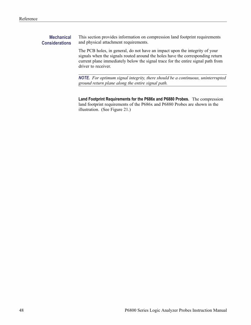
Reference
MechanicalConsiderations
This section provides information on compression land footprint requirementsand physical attachment requirements.
The PCB holes, in general, do not have an impact upon the integrity of yoursignals when the signals routed around the holes have the corresponding returncurrent plane immediately below the signal trace for the entire signal path fromdriver to receiver.
NOTE. For optimum signal integrity, there should be a continuous, uninterruptedground return plane along the entire signal path.
Land Footprint Requirements for the P686x and P6880 Probes. The compressionland footprint requirements of the P686x and P6880 Probes are shown in theillustration. (See Figure 21.)
48 P6800 Series Logic Analyzer Probes Instruction Manual

Reference
Figure 21: Land footprint requirements for the P686x and P6880 probes (top view)
P6800 Series Logic Analyzer Probes Instruction Manual 49

Reference
Special Considerations
WARNING. To avoid personal injury due to electric shock, always turn off thepower on your target system before cleaning the compression footprint.
Cleanliness is important for a reliable connection. (See page 13, Cleaning theP686x and P6880 Compression Footprints.)
Line boxes around the pin groupings are the via keepout areas (not part of theactual land footprint).
Solder mask is required between all land pads in the component keepout area.
All signal runs in the keepout areas are required to maintain PCB and soldermask tolerances to ensure that no exposed runs or metal exist between pads.This requirement avoids the risk of shorting signal runs.
Solder mask hardness of at least 8H (pencil hardness) and thickness of atleast 0.0762 mm to 0.1270 mm (0.0003 to 0.0005 in) has been verified forseveral hundred cycles without appreciable wear from the compressioncontact cycling.
The compression land footprint design was verified on the immersion goldprocess.
Land Footprint Requirements for the Compression-on-PCB to P6434 MictorAdapter. The following two figures show the land footprint requirements of theCompression-on-PCB to P6434 Mictor adapter. (See Figure 22 on page 51.)(See Figure 23 on page 51.) This compression adapter converts from the newcompression footprint to the existing P6434 Mictor-based 34-channel probe.
Refer to the P6434 Mass Termination Probe Manual for the Mictor land footprintspecification. The recommended channel mappings for the Compression-on-PCBto P6434 Mictor adapter and Mictor-on-PCB to Compression adapter is listed.(See Table 13 on page 37.)
50 P6800 Series Logic Analyzer Probes Instruction Manual

Reference
Figure 22: Land footprint requirements for the 34-channel Compression-on-PCBto P6434 Mictor adapter
Figure 23: Land footprint requirements for the 17-channel Compression-on-PCBto P6434 Mictor adapter
P6800 Series Logic Analyzer Probes Instruction Manual 51
Reference
Special Considerations
Two compression land footprints must be spaced as per the mechanicaldimensions specified to support the compression adapter.
Placement of the compression land footprints is only constrained with use ofthe compression adapter, not in normal usage of the TLA7Axx logic analyzerwith a High-Density Probe.
The P6434 Probe and older logic analyzer modules do not support differentialsignals. Therefore, the compression adapter cannot be used to supportdifferential signals beyond capturing each side of the differential signalindependently in a single-ended manner.
The compression adapter will add capacitance to the P6434 Probe inputcapacitance. The Mictor adapter adds 2.7 pF to the High-Density Compressionprobe load of 0.7 pF for a combined adapter capacitance load of 3.4 pF.
The TLA7Axx logic analyzer with the P6860 High-Density Probe will connectdirectly to the compression land footprint to support high performance datacapture and viewing needs.
The TLA7Axx logic analyzer with the P6880 High-Density Differential Probewill also connect directly to the compression land footprint to support highperformance differential signal capture and viewing needs.
Physical Attachment Requirements for the P6810 Probe. The physical dimensionsof the P6810 General Purpose Probe. (See Figure 24.)
Figure 24: Physical attachment requirements for the P6810 probe
52 P6800 Series Logic Analyzer Probes Instruction Manual

Reference
Physical Attachment Requirements for the P686x and P6880 Probes. Theconnector-less P686x High-Density Probe and P6880 High-Density DifferentialProbe interconnects are designed to accommodate PCB thickness ranging from1.27 mm to 3.81 mm (0.050 in to 0.150 in). To accommodate this range, thereare two versions of the design.
Nut bar–If the PCB thickness is 1.27 mm to 2.36 mm (0.050 in to 0.093 in),use the nut bar with the thin elastomer. (See Figure 25.)
Press-in nut–If the PCB thickness is 2.36 mm to 3.81 mm (0.093 in to0.150 in), use the press-in nut with the thick elastomer. (See Figure 26 onpage 54.)
Figure 25: Nut Bar design
P6800 Series Logic Analyzer Probes Instruction Manual 53

Reference
Special Considerations for the Nut Bar Design
The nut bar backing plate is required to maintain PCB flatness, which supportsthe compression connection.
The nut bar snaps in and out of the PCB without the use of tools.
Nut bars are reusable and are not required to be a permanent part of the PCB.
The elastomer used is independent and replaceable.
Additional nut bars and both thick and thin elastomer holders may be orderedfrom Tektronix.
Figure 26: Press-in Nut design
Special Considerations for the Press-in Nut Design
The PEM® KF2 2-56 or equivalent press-in nut must be inserted into the PCB.
The elastomer used is independent and replaceable.
Physical Attachment Requirements for the Compression-on-PCB to P6434 Mictorand Mictor-on-PCB to P6860 Compression Adapters. You can get the mechanicaldimensions of the adapters in the Mictor-on-PCB to P6860 Compression Adaptersection. (See Figure 6 on page 9.) (See Figure 7 on page 10.)
54 P6800 Series Logic Analyzer Probes Instruction Manual

Reference
Electrical Considerations This section provides information on transmission lines and load models forthe P6810 General Purpose, P686x High-Density, and P6880 High-DensityDifferential Probes.
The low frequency model is typically adequate for rise and fall times of 1 nsor greater in a typical 25 Ω source impedance environment (50 Ω runs with apass-through connection). For source impedance outside this range, and/or riseand fall times less than 1 ns, use the high frequency model to determine if asignificant difference is obtained in the modeling result.
The compression land pattern pad is not part of the load model. Make sure thatyou include the compression land pad and in the modeling.
Transmission Lines. Due to the high performance nature of the interconnect,ensure that stubs, which are greater than 1/4 length of the signal rise time, bemodeled as transmission lines.
P6810 General Purpose Probe Load Model. The following electrical modeldisplays a single podlet load model of the General Purpose Probes. (SeeFigure 27.)
Figure 27: Single podlet load model
P6800 Series Logic Analyzer Probes Instruction Manual 55

Reference
The characteristics listed in the following table apply to single podlets and theleadsets shown in the illustrations. (See Figure 28.) (See Figure 29.) (SeeFigure 30.) Note the differences in the characteristics when podlets are usedwith leadsets.
Table 16: P6810 General Purpose Probe performance with single podlet and leadsetsCharacteristic Single podlet only Single podlet with leadsetsMaximum clock speed 450 MHz when used with TLA7Axx modules
1.4 GHz when used with TLA7Bxx modules50 MHz (single-ended leadset), one groundlead connected90 - 100 MHz (single-ended leadset), twoground leads connected150 - 200 MHz (differential leadset)
AC loading Refer to the single podlet load model. (SeeFigure 27 on page 55.)
< 5 pF per channel as seen by the deviceunder test
DC loading 20 kΩ to ground 20 kΩ to groundIsolation N/A. Each signal lead on the eight-channel leadset
contains a 150 Ω series termination near theend of the barrel connector to minimize signalreflections.
Dimensions (See Figure 24 on page 52.) (See Figure 28.) (See Figure 29 on page 57.)(See Figure 30 on page 57.)
Recommended usage High-performance probing for single-endedor differential signals.
TTL and CMOS levels only. Ground leadsshould be connected to ground of the SUT.Not recommended for signals with edge rates> 1 V/ns.
Figure 28: Eight-channel leadset (barrel connectors)
56 P6800 Series Logic Analyzer Probes Instruction Manual

Reference
Figure 29: One-channel leadset (barrel connector)
Figure 30: Eight-channel differential leadset
P686x High-Density and P6880 High-Density Differential Probes Load Model. Thefollowing electrical model includes a low-frequency and high-frequency modelof the High-Density and High-Density Differential Probes. (See Figure 31.) Forthe Differential Probe, the load model is applied to both the + side and the –side of the signal.
P6800 Series Logic Analyzer Probes Instruction Manual 57

Reference
Figure 31: High-Density and High-Density Differential probe load model
The differential load for the P686x clock input and the P6880 probe can bemodeled by attaching the single line model to each side (+ and –) of the differentialsignal. The + and – sides of the differential signal are well insulated in the probehead up to and including the differential input stage.
Mictor-on-PCB to P6860 Compression Adapter Load Model. Refer the followingillustration for an electrical model of the Mictor-on-PCB to P6860 Compressionadapter. (See Figure 32.) The pad cap is the capacitance of the 0.016 in x 0.032 inpad of the P6860/P6880 compression land footprint. The capacitive load dependsupon the distance to the underlying conductors.
Figure 32: Mictor-on-PCB to Compression adapter load model
58 P6800 Series Logic Analyzer Probes Instruction Manual

Reference
Compression-on-PCB to P6434 Mictor Adapter Load Model. Refer to the followingillustration for an electrical model of the Compression-on-PCB to P6434 Mictoradapter. (See Figure 33.) The pad cap is the capacitance of the 0.016 in x 0.032 inpad of the P6860/P6880 compression land footprint. The capacitive load dependsupon the distance to the underlying conductors.
Figure 33: Compression-on-PCB to P6434 Mictor adapter load model
P6800 Series Logic Analyzer Probes Instruction Manual 59

Reference
60 P6800 Series Logic Analyzer Probes Instruction Manual

Specifications
Mechanical and Electrical SpecificationsThe mechanical and electrical specifications for the P6810, P686x, and P6880Probes are listed. (See Table 17.) The electrical specifications apply when theprobe is connected between a compatible logic analyzer and a target system.
Refer to the Tektronix Logic Analyzer Family Product Specifications document(Tektronix part number 071-1344-xx) available on the Tektronix Logic AnalyzerFamily Product Documentation CD or downloadable from the Tektronix Web sitefor a complete list of specifications, including overall system specifications.
Table 17: Mechanical and electrical specificationsCharacteristic P6810 P6860/P6864 P6880Threshold accuracy ±(35 mV ±1% of
setting)±(35 mV ±1% ofsetting)
±(35 mV ±1% ofsetting)
Input resistance 20 kΩ ±1% 20 kΩ ±1% 20 kΩ ±1%Input capacitance <1.0 pF 1 0.7 pF (typical) 0.7 pF (typical)Minimum digitalsignal swing
300 mVsingle-ended
300 mVsingle-ended
150 mV differentialeach side
Maximumnondestructiveinput signal to probe
±15 V ±15 V ±15 V
Delay from probetip to module inputconnector
7.70 ns ±80 ps 7.70 ns ±60 ps 7.70 ns ±80 ps
Probe length 1.8 m (6 ft) 1.8 m (6 ft) 1.8 m (6 ft)Operating range +5 V to –2.5 V +5 V to –2.5 V +5 V to –2.5 V1 P6810 single podlet input capacitance is 0.7 pF, but podlets in a group will have 1 pF input capacitance.
NOTE. Because the length of all three probes are electrically similar, they can beinterchanged without problems.
P6800 Series Logic Analyzer Probes Instruction Manual 61

Specifications
The probes are designed to meet Tektronix standard 062-2847-00 class 5. Theenvironmental specifications for all three probes are listed. (See Table 18.)
Table 18: Environmental specificationsCharacteristic P6810, P6860/P6864, and P6880Temperature
Operating 0 °C to +50 °CNonoperating –51 °C to 71 °C
Humidity 10 °C to 30 °C, 95% relative humidity30 °C to 40 °C, 75% relative humidity40 °C to 50 °C, 45% relative humidity
AltitudeOperating 10,000 ft (3,048 m)Nonoperating 40,000 ft (12,192 m)
Electrostatic immunity 6 kV
62 P6800 Series Logic Analyzer Probes Instruction Manual

MaintenanceThe P6810, P686x, and P6880 Probes do not require scheduled or periodicmaintenance. Refer to the Functional Check section below to verify the basicfunctionality of the probes.
To confirm that the probes meet or exceed the performance requirements forpublished specifications with a compatible logic analyzer module, refer to theTLA7ACx Logic Analyzer Module Service Manual and follow the procedureslisted under performance verification procedures.
Probe CalibrationIf you are performing the probe calibration yourself, refer to the TLA7ACxLogic Analyzer Module Service Manual for the complete calibration procedure.Otherwise, return the probe to the local Tektronix service center.
StrategyExcept for the elastomer holders, the P6810, P686x, and P6880 Probes containno user-replaceable parts. If probe failure occurs, return the entire probe to yourTektronix representative for repair.
Functional CheckConnect the logic analyzer probes to an active signal source. Open the Setupwindow for the module where the probes are attached. Check for signal activity inthe Setup window for the attached probe.
P6800 Series Logic Analyzer Probes Instruction Manual 63

Maintenance
Inspection and Cleaning
CAUTION. To prevent damage during the probe connection process, do not touchthe exposed edge of the elastomer.
To maintain a reliable electrical contact, keep the probes free of dirt, dust, andcontaminants. Remove dirt and dust with a soft brush. For more extensivecleaning, use only a damp cloth. Never use abrasive cleaners or organic solvents.
Repackaging InstructionsUse the original packaging, if possible, to return or store the probes. If theoriginal packaging is not available, use a corrugated cardboard shipping carton.Add cushioning material to prevent the probes from moving inside the shippingcontainer.
Enclose the following information when shipping the probe to a Tektronix Center.
Owner’s address
Name and phone number of a contact person
Type of probe
Reason for return
Full description of the required
64 P6800 Series Logic Analyzer Probes Instruction Manual
Replaceable PartsThis chapter contains a list of the replaceable components for the P6810, P686xand P6880 Probes. Use this list to identify and order replacement parts.
Parts Ordering InformationReplacement parts are available through your local Tektronix field office orrepresentative.
Changes to Tektronix products are sometimes made to accommodate improvedcomponents as they become available and to give you the benefit of the latestimprovements. Therefore, when ordering parts, it is important to include thefollowing information in your order.
Part number
Instrument type or model number
Instrument serial number
Instrument modification number, if applicable
If you order a part that has been replaced with a different or improved part, yourlocal Tektronix field office or representative will contact you concerning anychange in part number.
P6800 Series Logic Analyzer Probes Instruction Manual 65

Replaceable Parts
Using the Replaceable Parts ListReplaceable Parts The P6810 probe contains no user-replaceable parts, while the P686x and P6880
compression probes contain only the elastomer as a replaceable part. If probefailure occurs, return the entire probe to your Tektronix representative for repair.
Refer to the following list for replaceable items:
Table 19: Parts list column descriptionsColumn Column name Description1 Figure & index number Items in this section
reference figure and indexnumbers to the explodedview illustrations that follow.
2 Tektronix part number Use this part number whenordering replacement partsfrom Tektronix.
3 and 4 Serial number Column three indicatesthe serial number at whichthe part was first effective.Column four indicates theserial number at which thepart was discontinued. Noentries indicate that thepart is good for all serialnumbers.
5 Qty This indicates the quantityof parts used.
6 Name & description An item name is separatedfrom the description by acolon (:). Because of spacelimitations, an item namemay sometimes appear asincomplete. Use the U.S.Federal Catalog handbookH6-1 for further item nameidentification.
Abbreviations Abbreviations conform to American National Standard ANSI Y1.1-1972.
66 P6800 Series Logic Analyzer Probes Instruction Manual

Replaceable Parts
Table 20: P6810 replaceable parts listFigure& indexnumber
Tektronix partnumber
Serialno.effective
Serial no.discont’d Qty Name & description
34–1 010-6810-10 1 GENERAL PURPOSE PROBE (INCLUDES SHEETOF LABELS AND LABELING INSTRUCTIONS)
-5 352-1097-XX 4 PODLET HOLDERP6810 STANDARD ACCESSORIES
-2 196-3471-XX 2 P6810 LEADSET, 1 CH SINGLE-ENDED ANDDIFFERENTIAL
-3 196-3470-XX 4 P6810 LEADSET, 8 CH SINGLE-ENDEDSMG50 2 ADAPTER KIT; BAG OF 20 KLIPCHIP ADAPTER (40
TOTAL)071-1122-XX 1 MANUAL, TECH; INSTRUCTIONS, P6810 GENERAL
PURPOSE LOGIC ANALYZER PROBE LABEL
-4
335-0345-XX 1 P6810 PROBE, SHEET OF LABELS
Figure 34: P6810 General Purpose probe accessories
P6800 Series Logic Analyzer Probes Instruction Manual 67

Replaceable Parts
Table 21: P6860 replaceable parts listFigure& indexnumber
Tektronix partnumber
Serialno.effective
Serial no.discont’d Qty Name & description
35–1 010-6860-10 1 P6860 PROBE (INCLUDES SHEET OF LABELS ANDPROBE LABELING INSTRUCTIONS)
P6860 STANDARD ACCESSORIES-2 020-2451-XX 1 P6860 THIN ELASTOMER HOLDER ASSEMBLY,
(used with Nut Bar), BAG OF 2 (BLACK) (TOTAL OF 2ELASTOMER ASSEMBLIES)
020-2452-XX 1 P6860 THICK ELASTOMER HOLDER ASSEMBLY,(used with Press-in nuts), BAG OF 2 (GRAY) (TOTALOF 2 ELASTOMER ASSEMBLIES)
071-1123-XX 1 MANUAL, TECH; INSTRUCTIONS, P6860 HIGHDENSITY LOGIC ANALYZER PROBE LABEL
335-0346-XX 1 P6860 PROBE, SHEET OF LABELS
-3
220-0255-XX 1 NUT BAR ASSEMBLY
Figure 35: P6860 High-Density probe accessories
68 P6800 Series Logic Analyzer Probes Instruction Manual

Replaceable Parts
Table 22: P6864 replaceable parts listFigure& indexnumber
Tektronix partnumber
Serialno.effective
Serial no.discont’d Qty Name & description
36–1 010-6864-10 1 P6864 PROBE (INCLUDES SHEET OF LABELS ANDPROBE LABELING INSTRUCTIONS)
P6864 STANDARD ACCESSORIES-2 020-2451-XX 1 THIN ELASTOMER HOLDER ASSEMBLY, (used
with Nut Bar), BAG OF 2 (BLACK) (TOTAL OF 2ELASTOMER ASSEMBLIES)
020-2452-XX 1 THICK ELASTOMER HOLDER ASSEMBLY, (usedwith Press-in nuts), BAG OF 2 (GRAY) (TOTAL OF 2ELASTOMER ASSEMBLIES)
071-1313-XX 1 MANUAL, TECH; INSTRUCTIONS, P6864 HIGHDENSITY 4X LOGIC ANALYZER PROBE LABEL
335-1017-XX 1 P6864 PROBE, SHEET OF LABELS
-3
220-0255-XX 1 NUT BAR ASSEMBLY
Figure 36: P6864 High-Density 4X probe accessories
P6800 Series Logic Analyzer Probes Instruction Manual 69

Replaceable Parts
Table 23: P6880 replaceable parts listFigure& indexnumber
Tektronix partnumber
Serialno.effective
Serial no.discont’d Qty Name & description
37–1 010-6880-10 1 P6880 PROBE SET (INCLUDES SHEET OF LABELSAND PROBE LABELING INSTRUCTIONS)
P6880 STANDARD ACCESSORIES-2 020-2451-XX 2 P6880 THIN ELASTOMER HOLDER ASSEMBLY, (used
with the Nut Bar), BAG OF 2 (BLACK) (TOTAL OF 4ELASTOMER ASSEMBLIES)
020-2452-XX 2 P6880 THICK ELASTOMER HOLDER ASSEMBLY,(used with the Press-in nuts), BAG OF 2 (TEK SILVERGRAY). TOTAL OF 4 ELASTOMER ASSEMBLIES.
071-1124-XX 1 MANUAL, TECH; INSTRUCTIONS, P6880 HIGHDENSITY DIFFERENTIAL LOGIC ANALYZER PROBELABEL
335-0697-XX 1 SHEET OF LABELS, P6880 PROBE
-3
220-0255-XX 1 NUT BAR ASSEMBLY
Figure 37: P6880 High-Density Differential probe accessories
70 P6800 Series Logic Analyzer Probes Instruction Manual

Replaceable Parts
Table 24: Compression-on-PCB to P6434 Mictor Adapter partsFigure& indexnumber
Tektronix partnumber
Serialno.effective
Serial no.discont’d Qty Name & description
P6860 and P6880 OPTIONAL ACCESSORIES38–1 020-2453-00 1 NUT BAR ASSEMBLY, BAG OF 2-2 020-2455-XX 1 17 CH COMPRESSION-ON-PCB TO P6434 MICTOR
ADAPTER-3 020-2456-XX 1 34 CH COMPRESSION-ON-PCB TO P6434 MICTOR
ADAPTER-4 020-2457-XX 1 34 CH MICTOR-ON-PCB TO P6860 COMPRESSION
ADAPTER-5 352-1095-XX 1 ELASTOMER ASSEMBLY
Figure 38: Compression-on-PCB to P6434 Mictor Adapter parts
P6800 Series Logic Analyzer Probes Instruction Manual 71

Replaceable Parts
Table 25: P6810 optional accessoriesFigure& indexnumber
Tektronix partnumber
Serialno.effective
Serial no.discont’d Qty Name & description
39–1 196-3472-XX 4 P6810 LEADSET, 8 CH DIFFERENTIAL
Figure 39: P6810 optional accessories
72 P6800 Series Logic Analyzer Probes Instruction Manual

Index
Symbols and Numbers1-Channel single-ended and
differential leadset, 38-Channel differential leadset, 38-Channel single-ended and
differential leadset, 3
AAdapters
Compression on PCB toMictor, 10
Mictor on PCB toCompression, 8
CCalibration
probe, 63Cleaning
compression footprints, 13inspection and, 64probe heads, 14
ClockingSource Synchronus*, 24
Clocks, 23Commonly used terms, viCompression footprint, viCompression on PCB to Mictor
adapter, 10Connecting
probes to logic analyzer, 12probes to target system, 16
DDesigning an interface, 23
electrical considerations, 55land footprints, 44mechanical
considerations, 48signal names, 28
Differential input amplitudedefinition, vi
Documentationrelated, v
EElastomer holder, 18
installing Nutblock, 18installing Press-in nuts, 19
Electrical considerationsCompression-on-PCB to
P6434 Mictor adapter, 59Mictor-on-PCB to
Compression adapter, 58P6810 General Purpose Probe
load model, 55P686x Probe and P6880 Probe
load model, 57Transmission lines, 55
Electrical specifications, 61
FFootprints, land, 44
P6810 General PurposeProbe, 44
P686x High DensityProbe, 44
P6880 High DensityDifferential Probe, 46
Functional check, vi, 63
GGeneral Purpose Probe, P6810, 2
HHigh Density 4X Probe
P6864, 6High Density Differential Probe,
P6880, 7High Density Probe, P6860, 5High resolution timing modes, 27
Holderpodlet, vii
IInspection and cleaning, 64Installing
elastomer holder, 18
KKeepout area, vi
LLand footprints, 44
P6810 General PurposeProbe, 44
P686x High DensityProbe, 44
P6880 High DensityDifferential Probe, 46
Leadsets, 3impact on P6810 probe
performance, 56Load model
Compression-on-PCB toP6434 Mictor adapter, 59
Mictor-on-PCB toCompression adapter, 58
P6810 General PurposeProbe, 55
P686x and P6880 Probe, 57Logic analyzer
connecting probes, 12
MMaintenance, 63
functional check, 63inspection and cleaning, 64probe calibration, 63repackaging instructions, 64strategy, 63
P6800 Series Logic Analyzer Probes Instruction Manual 73

Index
Mechanical considerationsland footprint requirements for
the Compression on PCBto Mictor adapter, 50
land footprint requirementsfor the P686x and P6880Probes, 48
physical attachmentrequirements for P6810Probe, 52
physical attachmentrequirements for P686xand P6880 Probes, 53
physical attachmentrequirements for theCompression on PCBto Mictor and Mictoron PCB to Compressionadapters, 54
Mechanical specifications, 61Merged module, 24Mictor on PCB to Compression
adapter, 8
NNutblock, 18
OOrdering parts information, 65
PP6434 Mictor adapter, 10P6810 General Purpose Probe, 2
8-Channel differentialleadset, 3
8-Channel single-ended anddifferential leadset, 3
accessories, 3land footprints, 44leadsets, 3load model, 55performance
characteristics, 56single-ended and differential
leadset, 3
P6810 Probe General PurposeProbephysical attachment
requirements, 52P6860 High Density Probe, 5P6864 High Density 4X Probe, 6P686x and P6880 Probe
load model, 57P686x and P6880 Probes
cleaning the compressionfootprints, 13
cleaning the probe heads, 14land footprint
requirements, 48physical attachment
requirements for, 53storing the probe heads, 15
P686x High Density Probeland footprints, 44
P6880 High Density DifferentialProbe, 7land footprints, 46
Partsordering information, 65using the replaceable parts
list, 66PCB (printed circuit board), viiPodlet, viiPodlet holder, viiPress-in nuts, 19
Probesadapter, defined, viicalibration, 63cleaning the P686x and
P6880 Compressionfootprints, 13
cleaning the P686x and P6880probe heads, 14
connecting probes to the logicanalyzer, 12
connecting probes to the targetsystem, 16
head, defined, viiP6810 General Purpose
Probe, 2P6860 High Density Probe, 5P6864 High Density 4X
Probe, 6P6880 High Density
Differential Probe, 7product description, 1returning, 64storing, 64
Probing analog signals, 27Product description
Compression on PCB toMictor adapter, 10
Mictor on PCB toCompression adapter, 8
P6810 Leadset adapters andaccessories, 3
P6860 High Density Probe, 5P6864 High Density 4X
Probe, 6P6880 High Density
Differential Probe, 7
QQualifiers, 23
RRange recognition, 27Related documentation, vRepackaging instructions, 64
74 P6800 Series Logic Analyzer Probes Instruction Manual
Index
Requirementsland footprint for the
Compression on PCBto Mictor adapter, 50
land footprints for the P686xand P6880 Probes, 48
physical attachment for theCompression on PCBto Mictor and Mictoron PCB to Compressionadapters, 54
physical attachment for theP6810 Probe, 52
physical attachment forthe P686x and P6880Probes, 53
Returning probes, 64
SSignal connections, 23Signal fixturing, 23Signal names, 28SMT KlipChip, viiSpecifications
electrical, 61mechanical, 61
Storing probes, 64strategy, 63
TTarget system
connecting probes, 16Timing modes
High resolution, 27
Transmission Lines, 55
WWay station, viii
ZZ-axis elastomer, viii
P6800 Series Logic Analyzer Probes Instruction Manual 75