
P C C A R D S TA ND A R D - search read.pudn.comread.pudn.com/downloads60/ebook/208725/PC Card...
273
P C C A R D S TA N D A R D Volume 2 Electrical Specification
Transcript of P C C A R D S TA ND A R D - search read.pudn.comread.pudn.com/downloads60/ebook/208725/PC Card...

P C C A R D S TA N D A R D
Volume 2
Electrical Specification

PCMCIAJEIDA
©1999, PCMCIA/JEIDAAll rights reserved.
No part of this publication may bereproduced, stored in a retrievalsystem, or transmitted, in any form orby any means, mechanical,electronic, photocopying, recordingor otherwise, without prior writtenpermission of PCMCIA and JEIDA.Printed in the United States ofAmerica.
PCMCIA (Personal ComputerMemory Card InternationalAssociation)2635 North First Street, Suite 209San Jose, CA 95134 USA+1-408-433-2273+1-408-433-9558 (Fax)
JEIDA (Japan Electronic IndustryDevelopment Association)Kikai Shinko Kaikan, 3-5-8, ShibakoenMinato-ku, Tokyo 105, JAPAN+81-3-3433-1923+81-3-3433-6350 (Fax)
The PC Card logo and PC Card aretrademarks of PCMCIA, registered inthe United States. The PC Card logoand PC Card are trademarks ofJEIDA, registered in Japan.
PCMCIA HAS BEEN NOTIFIED BYCERTAIN THIRD PARTIES THATTHE IMPLEMENTATION OF THESTANDARD WILL REQUIRE ALICENSE FROM THOSE THIRDPARTIES TO AVOIDINFRINGEMENT OF THEIRRIGHTS. PCMCIA HAS OBTAINEDFROM SOME, BUT NOT ALL , OFTHOSE PARTIES A GRANT OFIMMUNITY THAT PCMCIA WILLEXTEND TO YOU, CONTINGENTUPON YOUR ENTERING INTOAND DELIVERING TO PCMCIATHE RECIPROCAL GRANT OFIMMUNITY AGREEMENTCONTAINED ELSEWHERE INTHIS STANDARD.
IMPORTANT:In order to receive the Grant ofImmunity, the owner of thisStandard must sign and return theenclosed Registration Card to:PCMCIA2635 North First Street, Suite 209San Jose, CA 95134 USA
NEITHER PCMCIA NOR JEIDAMAKES ANY WARRANTY,EXPRESS OR IMPLIED, WITHRESPECT TO THE STANDARD,INCLUDING AS TO NON-INFRINGEMENT,MERCHANTABILITY OR FITNESSFOR A PARTICULAR PURPOSE.THIS STANDARD IS PROVIDED TOYOU ÒAS IS.Ó
Document No. 0299-02-2000
First Printing, February 1999

ELECTRICAL SPECIFICATION
© 1999 PCMCIA/JEIDA iii
CONTENTS
1. Overview ______________________________________________11.1 Summary of Electrical Specification Changes....................................................................2
1.1.1 PCMCIA 2.0/JEIDA 4.1 (September 1991).......................................................................................................................2
1.1.2 PCMCIA 2.1/JEIDA 4.2 (July 1993)....................................................................................................................................2
1.1.3 PC Card Standard February 1995 Release (Release 5.0) ............................................................................................2
1.1.4 PC Card Standard March 1995 Update (Release 5.01)...............................................................................................3
1.1.5 PC Card Standard May 1995 Update (Release 5.02)...................................................................................................3
1.1.6 PC Card Standard November 1995 Update (Release 5.1)..........................................................................................3
1.1.7 PC Card Standard May 1996 Update (Release 5.2) .....................................................................................................3
1.1.8 PC Card Standard 6.0 Release (March 1997) .................................................................................................................3
1.1.9 PC Card Standard 6.1 Release (April 1998)....................................................................................................................3
1.1.10 PC Card Standard 7.0 Release (February 1999)..........................................................................................................3
1.2 Conventions .........................................................................................................................31.2.1 Signal Naming............................................................................................................................................................................4
1.2.2 Numeric Representation..........................................................................................................................................................4
1.2.3 Bit Action Representation.......................................................................................................................................................4
1.2.4 Signal Summary........................................................................................................................................................................4
2. Common Pin Description________________________________52.1 Power and Ground Pins ......................................................................................................5
2.1.1 VCC and GND Pins....................................................................................................................................................................5
2.1.2 VPP1 and VPP2 Pins...................................................................................................................................................................5
2.2 Interface Configuration Pins ...............................................................................................62.2.1 Card Detect Pins (CD[2::1]# and CCD[2::1]#)..................................................................................................................6
2.2.2 Voltage Sense Pins (VS[2::1]# and CVS[2::1]) .................................................................................................................6
3. Card Type Detection Mechanism _________________________73.1 PC Card Encodings .............................................................................................................7
3.2 Socket Key Selection ............................................................................................................8
3.3 Graceful Rejection in 16Ðbit PC Card Only Sockets...........................................................8
3.4 Determining Card Type in CardBus PC Card Capable Sockets........................................9
4. 16-bit PC Card Electrical Interface _______________________114.1 Compatibility Issues .........................................................................................................11
4.1.1 RESET and WAIT# Support................................................................................................................................................11
4.1.2 VS1# replaces RFSH (pin 43)...............................................................................................................................................11
4.2 Pin Assignments................................................................................................................11
4.3 16-bit PC Card Features....................................................................................................14

CONTENTS
iv ©1999 PCMCIA/JEIDA
4.3.1 Memory Address Space........................................................................................................................................................14
4.3.2 Memory Only Interface .........................................................................................................................................................15
4.3.3 I/O Address Space..................................................................................................................................................................15
4.3.4 I/O Interface ..............................................................................................................................................................................16
4.3.5 Custom Interfaces ....................................................................................................................................................................16
4.3.6 Configurable Cards................................................................................................................................................................17
4.4 Signal Description..............................................................................................................174.4.1 Address BUS (A[25::0]).........................................................................................................................................................17
4.4.2 Data BUS (D[15::0]) ................................................................................................................................................................17
4.4.3 Card Enable (CE[2::1]#)........................................................................................................................................................17
4.4.4 Output Enable (OE#) ..............................................................................................................................................................18
4.4.5 Write Enable (WE#)................................................................................................................................................................18
4.4.6 Ready (READY).......................................................................................................................................................................18
4.4.7 Interrupt Request (IREQ#) [I/O and Memory Interface]...........................................................................................19
4.4.7.1 Interrupt Request Routing......................................................................................................................................19
4.4.7.2 Level and Pulsed Mode Interrupt Support......................................................................................................20
4.4.7.2.1 Level Mode Interrupt Signal ......................................................................................................................20
4.4.7.2.2 Pulsed Mode Interrupt Signal....................................................................................................................20
4.4.8 Card Detect (CD[2::1]#) .........................................................................................................................................................21
4.4.9 Write Protect (WP) [Memory Only Interface]................................................................................................................21
4.4.10 I/O Is 16 Bit Port (IOIS16#) [I/O and Memory Interface].....................................................................................21
4.4.11 Attribute Memory Select (REG#)....................................................................................................................................21
4.4.12 Battery Voltage Detect (BVD[2::1]) [Memory Only Interface].............................................................................22
4.4.13 Status Changed (STSCHG#) [I/O and Memory Interface] ....................................................................................22
4.4.14 Audio Digital Waveform (SPKR#) [I/O and Memory Interface].......................................................................22
4.4.15 Program and Peripheral Voltages (VPP[2::1]) ............................................................................................................23
4.4.16 Voltage and Ground (VCC & GND)...............................................................................................................................23
4.4.16.1 Socket VCC for CIS Read......................................................................................................................................23
4.4.16.2 PC Card VCC for CIS Read..................................................................................................................................24
4.4.16.3 Changing PC Card VCC........................................................................................................................................24
4.4.17 Voltage Sense (VS[2::1]#) ...................................................................................................................................................24
4.4.18 I/O Read (IORD#) [I/O and Memory Interface] .......................................................................................................25
4.4.19 I/O Write (IOWR#) [I/O and Memory Interface] .....................................................................................................25
4.4.20 Card Reset (RESET).............................................................................................................................................................26
4.4.21 Extend Bus Cycle (WAIT#)................................................................................................................................................26
4.4.22 Input Port Acknowledge (INPACK#) [I/O and Memory Interface] ...................................................................26
4.5 DMA Signals Replacing I/O Interface Signals.................................................................264.5.1 DMA Request (DREQ#).........................................................................................................................................................26
4.5.2 DMA Acknowledge (DACK) [replaces REG#].............................................................................................................27
4.5.3 DMA Read (IOWR#)..............................................................................................................................................................27
4.5.4 DMA Write (IORD#)..............................................................................................................................................................27
4.5.5 Terminal Count (TC#)............................................................................................................................................................27
4.6 Memory Function...............................................................................................................274.6.1 Common Memory Function.................................................................................................................................................27

ELECTRICAL SPECIFICATION
© 1999 PCMCIA/JEIDA v
4.6.1.1 Common Memory Read Function for PC Cards ...........................................................................................27
4.6.1.2 Common Memory Write Function for PC Cards ..........................................................................................28
4.6.1.3 Common Memory Write Function for OTPROM, EPROM and Flash Memory...............................28
4.6.2 Attribute Memory Function.................................................................................................................................................28
4.6.2.1 Attribute Memory Read Function ......................................................................................................................29
4.6.2.2 Attribute Memory Write Function .....................................................................................................................29
4.6.2.3 Attribute Memory Write Function for Dual Supply OTPROM, EPROM and Flash Memory.....29
4.6.3 Write Protect Function...........................................................................................................................................................30
4.7 Timing Functions...............................................................................................................304.7.1 Common Memory Read Timing........................................................................................................................................30
4.7.2 Common and Attribute Memory Write Timing..........................................................................................................32
4.7.2.1 Common Memory Write Timing........................................................................................................................33
4.7.3 Attribute Memory Read Timing Specification.............................................................................................................33
4.7.4 Attribute Memory Write Timing Specification............................................................................................................33
4.7.5 Memory Timing Diagrams.................................................................................................................................................34
4.8 DMA Function...................................................................................................................354.8.1 DMA Read Function (Memory Read - I/O Write) ......................................................................................................36
4.8.2 DMA Read Timing (Memory Read - I/O Write).........................................................................................................36
4.8.3 DMA Write Function (I/O Read - Memory Write) .....................................................................................................37
4.8.4 DMA Write Timing (I/O Read - Memory Write)........................................................................................................38
4.9 Electrical Interface .............................................................................................................394.9.1 Signal Interface.........................................................................................................................................................................39
4.9.2 Memory Address Decoding................................................................................................................................................40
4.9.2.1 Function Configuration Registers Address Decoding................................................................................41
4.9.3 I/O Address Space Decoding .............................................................................................................................................41
4.9.3.1 Independent I/O Address Window..................................................................................................................41
4.9.3.2 Overlapping I/O Address Window..................................................................................................................42
4.10 Card Detect......................................................................................................................43
4.11 Battery Voltage Detect ....................................................................................................43
4.12 Power-up and Power-down............................................................................................444.12.1 Power-up/Power-down Timing.....................................................................................................................................44
4.12.2 Average Current During Card Configuration............................................................................................................45
4.12.3 Data Retention........................................................................................................................................................................46
4.12.4 Supplement ..............................................................................................................................................................................46
4.13 I/O Function....................................................................................................................464.13.1 I/O Transfer Function.........................................................................................................................................................46
4.13.2 I/O Input Function for I/O Cards...................................................................................................................................46
4.13.3 I/O Output Function for I/O Cards................................................................................................................................47
4.13.4 I/O Read (Input) Timing Specification.........................................................................................................................48
4.13.5 I/O Write (Output) Timing Specification.....................................................................................................................50
4.14 Function Configuration ...................................................................................................514.14.1 Overview..................................................................................................................................................................................51
4.14.2 Single Function PC Cards...................................................................................................................................................51

CONTENTS
vi ©1999 PCMCIA/JEIDA
4.14.3 Multiple Function PC Cards..............................................................................................................................................51
4.14.4 Function Configuration Registers (FCRs).....................................................................................................................52
4.15 Card Configuration .........................................................................................................534.15.1 Configuration Option Register.........................................................................................................................................54
4.15.2 Configuration and Status Register .................................................................................................................................56
4.15.3 Pin Replacement Register ...................................................................................................................................................58
4.15.4 Socket and Copy Register...................................................................................................................................................59
4.15.5 Extended Status Register ...................................................................................................................................................59
4.15.6 I/O Base Registers (0 .. 3) ...................................................................................................................................................60
4.15.7 I/O Limit Register ................................................................................................................................................................60
4.15.8 Power Management Support Register...........................................................................................................................61
4.15.9 Address Extension Registers............................................................................................................................................62
4.16 Indirect Access to PC Card Memory ..............................................................................64
5. CardBus PC Card Electrical Interface ____________________ 675.1 CardBus PC Card Signal Description...............................................................................67
5.1.1 Pin Assignments.......................................................................................................................................................................68
5.1.2 Signal/Pin Description..........................................................................................................................................................72
5.1.2.1 System Pins.................................................................................................................................................................72
5.1.2.2 Address and Data Pins..........................................................................................................................................72
5.1.2.3 Interface Control Pins..............................................................................................................................................73
5.1.2.4 Arbitration Pins (Bus Masters Only) ................................................................................................................73
5.1.2.5 Error Reporting Pins...............................................................................................................................................74
5.1.2.6 Interrupt Request Pin...............................................................................................................................................74
5.1.2.7 Additional Signals ..................................................................................................................................................74
5.1.3 Central Resource Functions..................................................................................................................................................75
5.2 CardBus PC Card Operation............................................................................................755.2.1 Bus Commands........................................................................................................................................................................75
5.2.1.1 Command Definition..............................................................................................................................................75
5.2.1.2 Command Usage Rules..........................................................................................................................................77
5.2.2 CardBus PC Card Protocol Fundamentals....................................................................................................................78
5.2.2.1 Basic Transfer Control ...........................................................................................................................................79
5.2.2.2 Addressing.................................................................................................................................................................79
5.2.2.3 Byte Alignment..........................................................................................................................................................81
5.2.2.4 Bus Driving and Turnaround..............................................................................................................................8 1
5.2.3 Bus Transactions .....................................................................................................................................................................82
5.2.3.1 Read Transaction .....................................................................................................................................................82
5.2.3.2 Write Transaction....................................................................................................................................................84
5.2.3.3 Transaction Termination......................................................................................................................................84
5.2.3.3.1 Master Initiated Termination....................................................................................................................85
5.2.3.3.2 Target Initiated Termination.....................................................................................................................87
5.2.4 Arbitration.................................................................................................................................................................................91
5.2.5 Arbitration Signaling Protocol ..........................................................................................................................................91
5.2.5.1 Fast Back-to-Back Transactions.........................................................................................................................93
ELECTRICAL SPECIFICATION
© 1999 PCMCIA/JEIDA vii
5.2.5.2 CardBus PC Card Idle Condition.......................................................................................................................95
5.2.5.3 Latency.........................................................................................................................................................................95
5.2.5.3.1 Managing Latency on CardBus PC Card..............................................................................................95
5.2.5.3.2 Low Latency Design Guidelines...............................................................................................................96
5.2.6 Exclusive Access ......................................................................................................................................................................97
5.2.6.1 Starting an Exclusive Access................................................................................................................................99
5.2.6.2 Continuing an Exclusive Access.......................................................................................................................100
5.2.6.3 Accessing a Locked Agent..................................................................................................................................101
5.2.6.4 Completing an Exclusive Access......................................................................................................................102
5.2.6.5 Supporting CBLOCK# and Write-back Cache Coherency......................................................................102
5.2.6.6 Complete Bus Lock................................................................................................................................................103
5.2.7 Other Bus Operations..........................................................................................................................................................103
5.2.7.1 Device Selection......................................................................................................................................................103
5.2.7.2 Special Cycle............................................................................................................................................................104
5.2.7.3 Address/Data Stepping......................................................................................................................................105
5.2.7.4 Configuration Cycle..............................................................................................................................................106
5.2.7.4.1 Generating Configuration Cycles..........................................................................................................108
5.2.7.4.1.1 Configuration Mechanism...........................................................................................................108
5.2.7.4.1.2 Generating Special Cycles with the Configuration Mechanism ....................................110
5.2.8 Error Functions .....................................................................................................................................................................110
5.2.8.1 Parity..........................................................................................................................................................................110
5.2.8.2 Error Reporting......................................................................................................................................................112
5.2.8.2.1 Parity Error Response and Reporting on CPERR#..........................................................................112
5.2.8.2.2 Error Response and Reporting on CSERR#.......................................................................................113
5.2.9 Cache Support ........................................................................................................................................................................114
5.2.10 Clock Control.......................................................................................................................................................................116
5.2.10.1 Clock Frequency...................................................................................................................................................116
5.2.10.2 Clock Control Protocol......................................................................................................................................116
5.2.10.2.1 Clock Stop or Slow down......................................................................................................................117
5.2.10.2.2 Clock Restart or Speed up......................................................................................................................117
5.2.10.2.3 Maintaining the Interface Clock..........................................................................................................118
5.2.11 Status Changed Notification..........................................................................................................................................119
5.2.11.1 Card Status Changed.........................................................................................................................................119
5.2.11.2 System and Interface Wake up .......................................................................................................................119
5.2.11.3 Register Descriptions.........................................................................................................................................121
5.2.11.3.1 Function Event Register ..........................................................................................................................121
5.2.11.3.2 Function Event Mask Register..............................................................................................................123
5.2.11.3.3 Function Present State Register ............................................................................................................125
5.2.11.3.4 Force Event Capability............................................................................................................................126
5.2.11.3.5 Default Field Values ................................................................................................................................128
5.2.12 Card Audio..........................................................................................................................................................................128
5.2.13 Special Design Considerations.....................................................................................................................................129
5.2.13.1 Multiple Retry Termination............................................................................................................................129
5.3 CardBus PC Card Electrical Specification......................................................................1295.3.1 Overview.................................................................................................................................................................................129

CONTENTS
viii ©1999 PCMCIA/JEIDA
5.3.1.1 Dynamic vs. Static Drive Specification .........................................................................................................130
5.3.2 Component Specifications .................................................................................................................................................130
5.3.2.1 3.3 V Signaling Environment............................................................................................................................131
5.3.2.1.1 DC Specifications.........................................................................................................................................131
5.3.2.1.2 AC Specifications.........................................................................................................................................132
5.3.2.1.3 CSTSCHG Buffer Specification...............................................................................................................132
5.3.2.1.4 CCLK AC Specifications ...........................................................................................................................132
5.3.2.1.5 Maximum AC Ratings and Device Protection (CCLK) .................................................................133
5.3.2.1.6 Noise Considerations.................................................................................................................................134
5.3.2.2 Timing Specification............................................................................................................................................135
5.3.2.2.1 Clock Specifications....................................................................................................................................135
5.3.2.2.2 Timing Parameters .....................................................................................................................................136
5.3.2.2.3 Measurement and Test Conditions.......................................................................................................137
5.3.2.3 Vendor Provided Specifications......................................................................................................................138
5.3.3 System (Motherboard) Specifications ..........................................................................................................................138
5.3.3.1 Clock Skew...............................................................................................................................................................138
5.3.3.2 Reset............................................................................................................................................................................139
5.3.3.3 Pull-ups......................................................................................................................................................................140
5.3.3.3.1 Pull-up Values for Control Signals .......................................................................................................141
5.3.3.3.2 Pull-up Values for Card Detect and Voltage Sense Pins ...............................................................141
5.3.3.3.3 Pull-up Resistor Requirements................................................................................................................142
5.3.3.4 Power Sequencing..................................................................................................................................................145
5.3.3.5 System Timing Budget ........................................................................................................................................145
5.3.3.6 Physical Requirements.........................................................................................................................................145
5.3.3.6.1 Routing and Layout of Four Layer Boards .......................................................................................145
5.3.3.6.2 Motherboard Impedance..........................................................................................................................145
5.3.4 CardBus PC Card Specifications ....................................................................................................................................146
5.3.4.1 Power Requirements.............................................................................................................................................146
5.3.4.1.1 Decoupling.....................................................................................................................................................146
5.3.4.1.2 External Power Supplies...........................................................................................................................146
5.3.4.2 Physical Requirements.........................................................................................................................................146
5.3.4.2.1 Trace Length Limits ...................................................................................................................................146
5.3.4.2.2 Impedance......................................................................................................................................................146
5.3.4.2.3 Signal Loading.............................................................................................................................................147
5.4 CardBus PC Card Programming Model.........................................................................1475.4.1 Overview.................................................................................................................................................................................147
5.4.2 Card Organization ..............................................................................................................................................................147
5.4.2.1 Configuration Space.............................................................................................................................................152
5.4.2.1.1 Command.......................................................................................................................................................155
5.4.2.1.2 Status................................................................................................................................................................156
5.4.2.1.3 Cache Line size .............................................................................................................................................158
5.4.2.1.4 Latency Timer...............................................................................................................................................158
5.4.2.1.5 Header Type..................................................................................................................................................159
5.4.2.1.6 Built-in Self Test (BIST).............................................................................................................................159
5.4.2.1.7 Base Address Register...............................................................................................................................159

ELECTRICAL SPECIFICATION
© 1999 PCMCIA/JEIDA ix
5.4.2.1.8 CIS Pointer......................................................................................................................................................161
5.4.2.1.9 Expansion ROM Base Address Register ............................................................................................162
5.4.2.1.10 Cap_Ptr .........................................................................................................................................................163
5.4.2.1.11 Interrupt Pin ................................................................................................................................................163
5.4.2.1.12 Tuple Space..................................................................................................................................................163
5.4.2.1.13 Register Summary....................................................................................................................................164
5.4.2.2 Memory Space ........................................................................................................................................................165
5.4.2.3 I/O Space..................................................................................................................................................................166
5.4.2.4 Expansion ROM.....................................................................................................................................................166
5.5 Requirements For CardBus PC Cards and Sockets........................................................1685.5.1 Overview.................................................................................................................................................................................168
5.5.2 Software Requirements ......................................................................................................................................................168
5.5.2.1 Socket Services........................................................................................................................................................168
5.5.2.2 Card Services ..........................................................................................................................................................169
5.5.2.3 System Resource Availability...........................................................................................................................169
5.5.2.4 System Resource Determination ......................................................................................................................169
5.5.2.5 Enabler Support .....................................................................................................................................................170
5.5.3 Card Requirements ..............................................................................................................................................................170
5.5.3.1 Configuration Space.............................................................................................................................................170
5.5.3.2 Required CIS............................................................................................................................................................170
5.5.3.3 Required Signals....................................................................................................................................................171
5.5.3.4 Pull-up/Pull-down Resistors............................................................................................................................171
5.5.3.5 CSTSCHG Support ................................................................................................................................................171
5.5.3.6 Power Consumption .............................................................................................................................................172
5.5.3.7 I/O Space Support .................................................................................................................................................172
5.5.4 Socket Requirements............................................................................................................................................................172
5.5.4.1 16-bit PC Card Support .......................................................................................................................................172
5.5.4.2 Address Spaces ......................................................................................................................................................173
5.5.4.2.1 Memory Space ..............................................................................................................................................173
5.5.4.2.2 I/O Support....................................................................................................................................................174
5.5.4.2.2.1 CardBus PC Card with Memory Mapped I/O....................................................................174
5.5.4.2.2.2 CardBus PC Card with I/O Space ............................................................................................174
5.5.4.2.2.3 ISA Support Implications.............................................................................................................175
5.5.4.3 Interrupt Handling and Routing......................................................................................................................175
5.5.4.3.1 Functional Interrupts (CINT#) ................................................................................................................175
5.5.4.3.2 Status Change Events.................................................................................................................................175
5.5.4.4 Register Descriptions...........................................................................................................................................176
5.5.4.4.1 Socket EVENT Register.............................................................................................................................176
5.5.4.4.2 Socket MASK Register...............................................................................................................................177
5.5.4.4.3 Socket PRESENT STATE Register ........................................................................................................178
5.5.4.4.4 FORCE Event Capability ..........................................................................................................................181
5.5.4.4.5 CONTROL Register ....................................................................................................................................183
5.5.4.5 VPP[2::1] Power Requirements ..........................................................................................................................183
5.5.4.6 Card Insertion and Removal.............................................................................................................................184
5.5.4.6.1 Card Insertion...............................................................................................................................................184

CONTENTS
x ©1999 PCMCIA/JEIDA
5.5.4.6.2 Card Removal...............................................................................................................................................185
5.5.4.7 Power Cycling the Interface ...............................................................................................................................186
5.5.4.7.1 Signal Requirements...................................................................................................................................186
5.5.4.7.2 CSTSCHG Requirements...........................................................................................................................186
5.5.4.7.3 In-Rush Current ............................................................................................................................................186
5.5.4.8 Required Pins ..........................................................................................................................................................187
5.5.4.9 Clock Stopping Support.......................................................................................................................................187
5.5.4.10 Special Cycle Support ........................................................................................................................................187
5.5.4.11 Actions When Adapter Is Reset......................................................................................................................187
6. PCI Bus Power Management Interface for CardBus Cards 1896.1 Introduction.....................................................................................................................189
6.1.1 Goals of this Specification.................................................................................................................................................189
6.1.2 Target Audience....................................................................................................................................................................190
6.1.3 Overview/Scope...................................................................................................................................................................190
6.1.4 Glossary of Terms................................................................................................................................................................192
6.1.5 Related Documents ..............................................................................................................................................................193
6.1.6 Conventions Used in this Chapter ..................................................................................................................................194
6.2 CardBus Power Management Overview.........................................................................1946.2.1 CardBus Power Management States.............................................................................................................................194
6.2.1.1 CardBus Function Power States.......................................................................................................................195
6.2.1.2 Bus Power States....................................................................................................................................................195
6.2.1.3 Device-Class Specifications ...............................................................................................................................195
6.2.1.4 Bus Support for CardBus Function Power Management........................................................................196
6.3 CardBus Power Management Interface..........................................................................1976.3.1 Capabilities List Data Structure .....................................................................................................................................198
6.3.1.1 Capabilities List Cap_Ptr Location................................................................................................................199
6.3.2 Power Management Register Block Definition.........................................................................................................200
6.3.2.1 Capability Identifier - Cap_ID (Offset = 0)...................................................................................................200
6.3.2.2 Next Item Pointer - Next_Item_Ptr (Offset = 1) ...........................................................................................201
6.3.2.3 PMC - Power Management Capabilities (Offset = 2)................................................................................201
6.3.2.4 PMCSR - Power Management Control/Status (Offset = 4) ....................................................................202
6.3.2.5 PMCSR_BSE - PMCSR PCI-to-PCI Bridge Support Extensions (Offset=6) Ð Not Used inCardBus Cards - Reserved....................................................................................................................................204
6.3.2.6 Data (Offset = 7) .....................................................................................................................................................205
6.4 CardBus Bus Power States .............................................................................................2076.4.1 CardBus B0 State - Fully On.............................................................................................................................................207
6.4.2 CardBus B1 State..................................................................................................................................................................208
6.4.3 CardBus B2 State..................................................................................................................................................................208
6.4.4 CardBus B3 State - Off........................................................................................................................................................208
6.4.5 CardBus Bus Power State Transitions .........................................................................................................................209
6.4.6 CardBus Clocking Considerations................................................................................................................................209
6.4.7 Control/Status of CardBus Bus Power Management States................................................................................210
6.4.7.1 Control of Secondary Bus Power Source and Clock.................................................................................210

ELECTRICAL SPECIFICATION
© 1999 PCMCIA/JEIDA xi
6.5 CardBus Function Power Management States...............................................................2116.5.1 CardBus Function D0 State...............................................................................................................................................211
6.5.2 CardBus Function D1 State...............................................................................................................................................212
6.5.3 CardBus Function D2 State...............................................................................................................................................212
6.5.4 CardBus Function D3 State...............................................................................................................................................212
6.5.4.1 Software Accessible D3 (D3hot).........................................................................................................................213
6.5.4.2 Power Off (D3cold)..................................................................................................................................................213
6.5.5 CardBus Function Power State Transitions ...............................................................................................................213
6.5.6 CardBus Card Function Power Management Policies ...........................................................................................215
6.5.6.1 State Transition Recovery Time Requirements ..........................................................................................219
6.6 CardBus Cards and Power Management.......................................................................2196.6.1 CardBus Card Context .......................................................................................................................................................222
6.6.2 PME_En/PME_Status and CardBus Cards ..............................................................................................................223
6.7 Power Management Events.............................................................................................2246.7.1 Auxiliary Power for D3cold Power Management Events .......................................................................................224
6.8 Software Support for PCI Power Management..............................................................2256.8.1 Identifying CardBus Function Capabilities................................................................................................................225
6.8.2 Placing CardBus Functions in a Low Power State...................................................................................................226
6.8.2.1 Buses...........................................................................................................................................................................226
6.8.2.2 D3 State .....................................................................................................................................................................226
6.8.3 Restoring PCI Functions From a Low Power State ..................................................................................................226
6.8.3.1 Dx States and the DSI Bit....................................................................................................................................226
6.8.3.2 D1 and D2 States ...................................................................................................................................................226
6.8.3.3 D3 State .....................................................................................................................................................................226
6.8.4 Wake Events ...........................................................................................................................................................................227
6.8.4.1 Wake Event Support .............................................................................................................................................227
6.8.4.2 The D0 "Initialized" State From a Wake Event...........................................................................................227
6.8.5 Get Capabilities.....................................................................................................................................................................228
6.8.6 Set Power State ......................................................................................................................................................................228
6.8.7 Get Power Status...................................................................................................................................................................228
6.9 Other Considerations.......................................................................................................228
7. Special Cycle Messages________________________________2297.1 Message Encodings..........................................................................................................229
7.2 Use of Specific Encodings ...............................................................................................229
8. CardBus PC Card Connector Test Methodology__________2318.1 Background......................................................................................................................231
8.2 Test Hardware Recommendations..................................................................................2318.2.1 General Recommendations...............................................................................................................................................231
8.2.2 Host-side Requirements .....................................................................................................................................................232
8.2.3 Card-side Recommendations ..........................................................................................................................................232
8.2.4 Measurement Equipment Recommendations ............................................................................................................232

CONTENTS
xii ©1999 PCMCIA/JEIDA
8.3 Test Board Considerations..............................................................................................2328.3.1 Host-side Implementation.................................................................................................................................................233
8.3.2 Card-side Implementation................................................................................................................................................234
8.4 Measurement Methodology.............................................................................................2358.4.1 Finding the Worst Case Ground Bounce......................................................................................................................235
9. PC Card Custom Interfaces____________________________ 2379.1 Custom Interface Requirements......................................................................................237
9.1.1 Purpose/Overview...............................................................................................................................................................237
9.1.2 Compatibility.........................................................................................................................................................................237
9.1.3 Pin Assignments....................................................................................................................................................................237
9.1.4 Features ....................................................................................................................................................................................237
9.1.5 Signal Description................................................................................................................................................................237
9.1.6 Functions..................................................................................................................................................................................238
9.1.7 Timing......................................................................................................................................................................................238
9.1.8 Electrical Interface ...............................................................................................................................................................238
9.1.9 Specific Signals and Functions........................................................................................................................................238
9.2 ZV Port Custom Interface (0141H).................................................................................2399.2.1 Overview.................................................................................................................................................................................239
9.2.2 Compatibility.........................................................................................................................................................................239
9.2.3 Pin Assignments....................................................................................................................................................................241
9.2.4 Features ....................................................................................................................................................................................243
9.2.5 Signal Description................................................................................................................................................................243
9.2.5.1 PCLK..........................................................................................................................................................................243
9.2.5.2 VSYNC.......................................................................................................................................................................243
9.2.5.3 HREF..........................................................................................................................................................................243
9.2.5.4 Y[7::0] .........................................................................................................................................................................243
9.2.5.5 UV[7::0] .....................................................................................................................................................................243
9.2.5.6 LRCLK.......................................................................................................................................................................243
9.2.5.7 SDATA......................................................................................................................................................................244
9.2.5.8 SCLK..........................................................................................................................................................................244
9.2.5.9 MCLK........................................................................................................................................................................244
9.2.6 Functions..................................................................................................................................................................................245
9.2.7 Timing......................................................................................................................................................................................245
9.2.7.1 Video Interface Timing .......................................................................................................................................245
9.2.7.2 Audio Interface Timing.......................................................................................................................................246
9.2.8 Electrical Interface ...............................................................................................................................................................246
9.2.9 Specific Signals and Functions........................................................................................................................................247
9.2.10 PC Card Connector Test Methodology......................................................................................................................247
9.3 DVB CI Port Custom Interface (0241h) .........................................................................2499.3.1 Overview.................................................................................................................................................................................249
9.3.2 Compatibility.........................................................................................................................................................................250
9.3.3 Pin Assignments....................................................................................................................................................................251
9.3.4 Features ....................................................................................................................................................................................252

ELECTRICAL SPECIFICATION
© 1999 PCMCIA/JEIDA xiii
9.3.5 Signal Description................................................................................................................................................................253
9.3.5.1 MDI[7::0]...................................................................................................................................................................253
9.3.5.2 MISTRT.....................................................................................................................................................................253
9.3.5.3 MIVAL......................................................................................................................................................................253
9.3.5.4 MDO[7::0].................................................................................................................................................................253
9.3.5.5 MOSTRT...................................................................................................................................................................253
9.3.5.6 MOVAL....................................................................................................................................................................253
9.3.5.7 MCLKI.......................................................................................................................................................................253
9.3.5.8 MCLKO.....................................................................................................................................................................253
9.3.6 Functions..................................................................................................................................................................................254
9.3.7 Timing......................................................................................................................................................................................254
9.3.8 Electrical Interface ...............................................................................................................................................................256
9.3.9 Specific Signals and Functions........................................................................................................................................256


ELECTRICAL SPECIFICATION
© 1999 PCMCIA/JEIDA xv
FIGURESFigure 3Ð1 CCD[2::1]# and CVS[2::1] Connections.....................................................................10
Figure 5-1 CardBus PC Card Basic Read Operation ...................................................................83
Figure 5-2 CardBus PC Card Basic Write Operation...................................................................84
Figure 5-3 CardBus PC Card Master Initiated Termination........................................................85
Figure 5-4 CardBus PC Card Master-abort Termination.............................................................87
Figure 5-5 Target Initiated Termination .......................................................................................90
Figure 5-6 CardBus PC Card Basic Arbitration...........................................................................92
Figure 5-7 Arbitration for Back-to-Back Access...........................................................................94
Figure 5-8 Components of Access Latency ..................................................................................95
Figure 5-9 CardBus PC Card Starting an Exclusive Access......................................................100
Figure 5-10 CardBus PC Card Continuing an Exclusive Access...............................................101
Figure 5-11 CardBus PC Card Accessing a Locked Agent........................................................102
Figure 5-12 CDEVSEL# Assertion..............................................................................................103
Figure 5-13 Address Stepping ....................................................................................................106
Figure 5-14 Type 0 and Type 1 Configuration Accesses ...........................................................107
Figure 5-15 Layout of CONFIG_ADDRESS Register ................................................................108
Figure 5-16 Bridge Translation for Type 0 Configuration Cycles..............................................109
Figure 5-17 Parity Operation ......................................................................................................111
Figure 5-18 CardBus PC Card Clock Stop or Slow Down.........................................................117
Figure 5-19 CardBus PC Card Clock Start or Speed up............................................................118
Figure 5-20 Maintaining CardBus PC Card Clock.....................................................................119
Figure 5-21: CardBus PC Card Function Event Register ...........................................................122
Figure 5-22: Function Event Mask Register ................................................................................123
Figure 5-23: Function Present State Register ..............................................................................125
Figure 5-24: Function Force Event Register.................................................................................127
Figure 5-25 V/I Curves for 3.3 V Signaling................................................................................133
Figure 5-26 Test Waveform for 3.3 V Signaling (CCLK) ...........................................................134
Figure 5-27 CardBus PC Card Clock Waveform .......................................................................135
Figure 5-28 Output Timing Measurement Conditions ..............................................................137
Figure 5-29 Input Timing Measurement Conditions..................................................................137
Figure 5-30 Clock Skew Diagram ...............................................................................................139
Figure 5-31 Reset Timing.............................................................................................................140

FIGURES
xvi ©1999 PCMCIA/JEIDA
Figure 5-32 Card with Memory and I/O Space in Host System with no Separate I/O Space149
Figure 5-33 Memory-only Card in Host System.........................................................................150
Figure 5-34 I/O Space-only Card in a Host System with a Separate I/O Space.....................151
Figure 5-35 Card and Host with All Spaces Described .............................................................152
Figure 5-36 CardBus PC Card Configuration Space .................................................................154
Figure 5-37 COMMAND Register Layout..................................................................................155
Figure 5-38: STATUS Register Layout .......................................................................................157
Figure 5-39 BIST Register............................................................................................................159
Figure 5-40 Base Address Register Mapping for Memory Space ..............................................160
Figure 5-41 Base Address Register Mapping for I/O Space .....................................................161
Figure 5-42 CIS POINTER Layout .............................................................................................161
Figure 5-43 Expansion ROM Base Address Register Layout ....................................................163
Figure 5-44 Socket EVENT Register............................................................................................176
Figure 5-45 Socket MASK Register .............................................................................................177
Figure 5-46 Socket PRESENT STATE Register...........................................................................179
Figure 5-47 Socket FORCE Register............................................................................................181
Figure 5-48 Socket CONTROL Register......................................................................................183
Figure 6-1: Operating System Directed Power Management System Architecture ..................191
Figure 6-2: Example "Originating Devices" ................................................................................192
Figure 6-3: Standard PCI Configuration Space Header Type 0 ................................................197
Figure 6-4: Capabilities Linked List............................................................................................199
Figure 6-5: Power Management Register Block ..........................................................................200
Figure 6-6: PCI Bus PM State Transitions..................................................................................209
Figure 6-7: PCI Function Power Management State Transitions...............................................214
Figure 6-8: Non-Bridge CardBus Function Power Management Diagram................................216
Figure 6-9: CardBus Card Power Management Diagram..........................................................220
Figure 6-10: Vcc to VAUX Transitioning .......................................................................................225
Figure 8Ð1 Host-side Test Board Layout ...................................................................................233
Figure 8Ð2 Card-side Test Board Layout...................................................................................234
Figure 9-1 Example ZV Port Implementation............................................................................239
Figure 9-2 ZV Port Signals on PC Card Socket ..........................................................................242
Figure 9-3: 1A I2S Format - MCLK = 256fs................................................................................244
Figure 9-4: 1B I2S Format - MCLK = 384fs ................................................................................244
Figure 9-5 Video Interface Timing ..............................................................................................245

ELECTRICAL SPECIFICATION
© 1999 PCMCIA/JEIDA xvii
Figure 9-6 Audio Interface Timing .............................................................................................246
Figure 9-7 Host-side Test Board Layout....................................................................................248
Figure 9-8: Example DVB CI Port Implementation...................................................................249
Figure 9-9: Transport Stream Interface Chaining between Modules .........................................250
Figure 9-10: DVB CI Port Signals on PC Card Socket ...............................................................252
Figure 9-11: Transport Data Stream Interface Timing...............................................................255


ELECTRICAL SPECIFICATION
© 1999 PCMCIA/JEIDA xix
TABLESTable 3Ð1 Card Detect and Voltage Sense Connections.................................................................8
Table 5Ð1 CardBus PC Card List of Signals ................................................................................68
Table 5Ð2 PC Card Pin 1 to Pin 34 Assignments.........................................................................70
Table 5Ð3 PC Card Pin 35 to Pin 68 Assignments.......................................................................71
Table 5Ð4 CardBus PC Card Commands ....................................................................................75
Table 5Ð5 Address Bus Encoding.................................................................................................80
Table 5Ð6 Common Access Field Definitions.............................................................................107
Table 5Ð7 DC Specification for 3.3 V Signaling..........................................................................131
Table 5Ð8 AC Specifications for 3.3 V Signaling........................................................................132
Table 5Ð9 AC Specification for 3.3 V Signaling (CCLK)............................................................133
Table 5Ð10 CardBus PC Card Clock Specifications...................................................................135
Table 5Ð11 3.3 V Timing Parameters..........................................................................................136
Table 5Ð12 Measurement and Test Condition Parameters........................................................137
Table 5Ð13 Clock Skew Parameters............................................................................................138
Table 5Ð14 Minimum and Maximum Pull-up Resistor Values (3.3 V signaling).....................141
Table 5Ð15 Pull-up/Pull-down Resistor Requirements .............................................................143
Table 5Ð16 Pull-up/Pull-down Resistor Requirements .............................................................144
Table 5Ð17 COMMAND Register Field Definitions ...................................................................156
Table 5Ð18 STATUS Register Field Definition............................................................................158
Table 5Ð19 BIST Register Fields..................................................................................................159
Table 5Ð20 Meaning of the Type Fields for a Memory Base Address Register .........................160
Table 5Ð21 Address Space Indicator Values..............................................................................162
Table 5Ð22 Address Space Offset Values ..................................................................................162
Table 5Ð23 Configuration Space Register Usage Summary ......................................................165
Table 5Ð24 Expansion ROM Image Header ...............................................................................166
Table 5Ð25 CardBus PC Card Data Structure Fields ................................................................167
Table 5Ð26 Code Type Descriptions...........................................................................................168
Table 5Ð27 Socket EVENT Register Fields..................................................................................177
Table 5Ð28 Socket MASK Register Fields ...................................................................................178
Table 5Ð29 Socket PRESENT STATE Register Fields.................................................................180
Table 5Ð30 Socket FORCE Register Fields..................................................................................182
Table 5Ð31 Socket CONTROL Register Fields............................................................................183

TABLES
xx ©1999 PCMCIA/JEIDA
Table 6-1: PCI Status Register ....................................................................................................198
Table 6-2: Capabilities Pointer - Cap_Ptr...................................................................................198
Table 6-3: PCI Configuration Space Header Type / Cap_Ptr mappings.................................199
Table 6-4: Capability Identifier - Cap_ID ..................................................................................200
Table 6-5: Next Item Pointer - Next_Item_Ptr...........................................................................201
Table 6-6: Power Management Capabilities Ð PMC for CardBus Cards ..................................202
Table 6-7: Power Management Control/Status - PMCSR .........................................................204
Table 6-8: PMCSR Bridge Support Extensions - PMCSR_BSE..................................................205
Table 6-9: Data Register..............................................................................................................205
Table 6-10: Power Consumption/Dissipation Reporting..........................................................206
Table 6-11: CardBus Bus Power Management States................................................................207
Table 6-12: PCI Bus Power and Clock Control ..........................................................................210
Table 6-13: State Diagram Summary.........................................................................................215
Table 6-14: D0 CardBus Card Power Management Policies .....................................................217
Table 6-15: D1 CardBus Card Power Management Policies .....................................................217
Table 6-16: D2 CardBus Card Power Management Policies .....................................................217
Table 6-17: D3hot CardBus Card Power Management Policies..................................................218
Table 6-18: D3cold CardBus Card Power Management Policies.................................................218
Table 6-19: CardBus Function State Transition Delays.............................................................219
Table 6-20: CardBus Card Power Management Policies ...........................................................221
Table 6-21: PME_En / PME_Status Summary in a CardBus Card..........................................223
Table 9-1 ZV Port Interface Pin Assignments ............................................................................241
Table 9-2 AC Parameters for Video Signals ...............................................................................246
Table 9-3 AC Parameters for Audio Signals ..............................................................................246
Table 9-4 ZV Port Electrical Interface.........................................................................................247
Table 9-5: DVB CI Port Interface Pin Assignments ...................................................................251
Table 9-6: Timing Relationship Limits........................................................................................255

ELECTRICAL SPECIFICATION
© 1999 PCMCIA/JEIDA 1
1 . O V E R V I E W
The Electrical Specification describes the connector pinout, interface protocol, signalingenvironment, interface timings, programming model, and specifics of card insertion, removal,power up, and configuration. It is organized in three sub-sections dealing with items common to allinterfaces, 16Ðbit PC Card interface specifics, and CardBus PC Card interface specifics.
The PC Card Standard continues an evolutionary process by providing additional capabilitiesthereby expanding the variety of PC Cards that can be supported. This release enables many typesof PC Cards ranging from 16Ðbit slave cards to 32Ðbit bus master cards, including multiple points inbetween such as 16Ðbit slave DMA and 32Ðbit slave cards. These capabilities provide higherperformance levels than previously available as well as new features such as card-to-card transferswithout intervention by the host CPU.
As a result, the spectrum of applications which can be supported by PC Cards has again beenbroadened. Just as PCMCIA 2.0 / JEIDA 4.1 evolved the PCMCIA 1.0 / JEIDA 4.0 memory onlyinterface by adding I/O capability, this new release evolves to include the capabilities outlinedbelow.
The capabilities of 16Ðbit PC Cards have been expanded and now provide:
• 16 bit data / 26 bit addressing.
• 20 MBytes/sec peak bandwidth at 100 ns cycle rate.
• support of 8Ðbit and 16Ðbit Slave DMA.
• compatibility with PCMCIA 2.1 / JEIDA 4.2 and earlier releases and CardBus PC Card Sockets.
• hardware detection of card voltage requirements (5 V, 3.3 V, X.X1 V).
• operation at 5 V, 3.3 V and X.X V voltage levels.
• support of multiple function cards.
• a Card Information Structure (CIS) with expanded capabilities to identify functions and dataformats. (See the Metaformat Specification.)
• a specification for current draw and time to READY.
There is an emerging class of applications which require higher performance - either 32Ðbitbandwidth, reduced latency via bus master capability, or both. However, there still exists a class ofapplications which remain better suited for the 16Ðbit environment because it already offerssufficient performance. This new release of the PC Card Standard has resolved this dilemma bydeveloping the CardBus PC Card interface which enables these new functions and still acceptscards developed to the 16Ðbit PC Card interface.
The CardBus PC Cards provide:
• 32Ðbit multiplexed address/data with parity.
• 132 MBytes/sec peak bandwidth at 33 MHz clock frequency.
• support for Bus Masters on PC Cards.
• synchronous interface.
• 3.3 V and lower voltage operation.
1 X.X V is less than 3.3 V

OVERVIEW
2 ©1999 PCMCIA/JEIDA
• support for remote system and/or interface wake up even when the interface is powered down.
• interface power management.
• compatibility with existing (PCMCIA 2.x/JEIDA 4.x) and new 16-bit PC Cards.
• the same PC Card mechanical form factors defined for all PC Cards.
• an enhanced 68-pin connector which provides improved signal grounding/noise reduction -- inaddition to CardBus PC Cards, the socket connector accepts all 16Ðbit PC Cards.
• ability to mix CardBus PC Cards and 16Ðbit PC Cards in sockets controlled by the sameCardBus PC Card adapter.
• hardware detection of the card type installed (CardBus PC Card vs. 16Ðbit PC Card).
• hardware detection of card voltage requirements (5 V, 3.3 V, X.X V2, Y.Y V3)
1.1 Summary of Electrical Specification Changes
1.1.1 PCMCIA 2.0/JEIDA 4.1 (September 1991)• added the I/O and Memory interface.
• defined the RESET signal.
• defined the WAIT# signal.
1.1.2 PCMCIA 2.1/JEIDA 4.2 (July 1993)The electrical section of the PCMCIA 2.1/JEIDA 4.2 release provided corrections to PCMCIA2.0/JEIDA 4.1.
1.1.3 PC Card Standard February 1995 Release (Release 5.0)• added the CardBus PC Card interface.
• changed the signal naming convention to denote an active-low signal with a Ò#Ó, (-REG is nowREG#).
• renamed the RDY/-BSY signal READY (with no change in function).
• redefined RFSH as voltage sense one (VS1#).
• defined the only RFU pin in the I/O and Memory interface as voltage sense two (VS2#).
• changed the I/O read (input) timing Ñ data delay from WAIT# rising, td(WT), from 35 ns to 0ns.
• defined DMA transfer cycles and use of signals for cards and sockets capable of DMAoperations.
• defined multiple voltage operation with initial operation at voltages other than 5 V.
• defined Multiple Function 16-bit PC Cards Ñ more than one set of configuration registers.
• defined the signal OFF states (use of pull-ups and switched VCC).
2 X.X V is less than 3.3 V3 Y.Y V is less than X.X V
ELECTRICAL SPECIFICATION
© 1999 PCMCIA/JEIDA 3
• specified the Card Configuration Register initialization sequence.
1.1.4 PC Card Standard March 1995 Update (Release 5.01)• general editorial corrections
1.1.5 PC Card Standard May 1995 Update (Release 5.02)• clarification of Power Waveforms at Power-on
1.1.6 PC Card Standard November 1995 Update (Release 5.1)• addition of Custom Interfaces for PC Cards
• addition of Indirect CIS Addressing for PC Cards
• clarifications for Multifunction PC Cards
1.1.7 PC Card Standard May 1996 Update (Release 5.2)• addition of the Zoomed Video (ZV) Port PC Card Custom Interface
1.1.8 PC Card Standard 6.0 Release (March 1997)• addition of the Thermal Ratings system for PC Cards
1.1.9 PC Card Standard 6.1 Release (April 1998)• The addition of the Small PC Card form factor, which adheres to the PC Card Standard
Electrical Specification except that the CardBus interface is not supported.
• addition of a Power Management interface for CardBus cards
1.1.10 PC Card Standard 7.0 Release (February 1999)• addition of the Digital Video Broadcasting (DVB) Port PC Card Custom Interface
• addition of the PC Card Memory Paging mechanism to extend the size of PC Card commonmemory space beyond 64 Mbytes
• corrections to the Power Management interface for CardBus cards
1.2 ConventionsThis section is intended to give general descriptions of notation conventions used in this document.(See also the Overview and Glossary.)
1.2.1 Signal NamingAll signals are named with respect to their asserted state as follows:
a) Each signal which is not a logic signal, such as VCC, has a name which does not end with a "#"character.

OVERVIEW
4 ©1999 PCMCIA/JEIDA
b) Each logic signal whose name does not end with a "#" character has logic high as the assertedstate and logic low as the negated state.
c) Each logic signal whose name ends with a "#" character has logic low as the asserted state andlogic high as the negated state.
1.2.2 Numeric RepresentationNumbers are expressed as follows:
a) Individual bits are expressed as "0" for zero, "1" for one, or "X" for "any value".
b) Groups of bits (fields) are expressed in hexadecimal number which begin with one or moredigits and are followed by an "H". Each digit represents 4 bits and is indicted by the characters"0" through "9" and "A" through "F" giving each digit a value of 0 to 15 (decimal). An "X" isused to indicate a digit of "any value". The number of bits in the field determines how manybits in the hexadecimal number are significant.
1.2.3 Bit Action RepresentationBits of a register are said to be set when they are made equal to "1" and to be reset when they aremade equal to "0" .
1.2.4 Signal SummarySignal Types:
in Input is a standard input-only signal.
out Totem Pole Output is a standard active driver.
i/o Input/Output is a bi-directional signal.
h/z High-Z is an output or I/O pin driver which is in the high impedance state when it is disabled.
s/h/z Sustained High-Z is an active low High-Z signal owned and driven by one and only one agent at a time.The agent that drives an s/h/z pin low must drive it high for at least one clock before letting it float. A newagent cannot start driving a s/h/z signal any sooner than one clock after the previous owner places it in aHigh-Z state. A pull-up is required to sustain the inactive state until another agent drives it, and must beprovided by the central resource.
o/d Open Drain allows multiple devices to share a signal as a wire-OR.
DC DC refers to power or ground pins which are not used for any information transfer.

ELECTRICAL SPECIFICATION
© 1999 PCMCIA/JEIDA 5
2 . C O M M O N P I N D E S C R I P T I O N
A number of pins have the same function for all three interfaces specified in this release: VCC,VPP[2::1], and GND. Several other pins are used for the same purpose in all three interfaces andhave similar function in terms of providing information about card presence, card type, and VCC
requirements. Signals whose function is specific to an interface are described in their respectivesections.
2.1 Power and Ground PinsPower and ground for all PC Card interfaces must be provided by the host system. PC Cards maynot apply any voltage to VCC, VPP[2::1], or GND. Refer to the Metaformat Specification forinformation on describing the cardÕs VCC and VPP[2::1] requirements in the Card InformationStructure.
2.1.1 VCC and GND PinsThe two 16Ðbit PC Card interfaces support 5 V, 3.3 V and X.X V VCC voltages while the CardBusPC Card interface supports 3.3 V, X.X V and Y.Y V VCC voltages. Deciding whether the sockethardware must support 5 V is a function of the interfaces being supported, the availability of 5 V inthe system, and which cards need to be enabled. Sockets are not required to support 5V VCC
operation. The connector places the two VCC pins (17 and 51) and four GND pins (1, 34, 35 and 68)at symmetrical positions on the connector.
The voltage level on VCC cannot be changed until the Card Information Structure (CIS) of the cardhas been read and other permissible values have been determined. If the CIS indicates the cardcould be operated at a different voltage level, the host can change to the new voltage level.
To change VCC, the host shall direct the socket to discharge the PC Card connectorÕs VCC andVPP[2::1] to ground, then power-up the card at the new voltage. Further, care should be takenwhen dynamically changing the voltage applied to VCC or VPP[2::1] so that power supply shorts donot occur. The host must recognize that the card will retain no knowledge of the power-up at theprevious VCC and all configuration and other initialization must be done following the secondpower-up. If any Card Detect pin is negated at any time, the host system must recognize that thecard may have been replaced and repeat the entire power-up sequence.
2.1.2 VPP1 and VPP2 PinsThe VPP[2::1] (pins 18 and 52) supply signals are used optionally on the card for PC Card operation.VPP[2::1] must be initially powered up at the voltage indicated by the voltage sense pins whichmeans systems are required to be able to supply the VCC level on the VPP[2::1] pins. The voltagelevel on VPP[2::1] cannot be changed until the Card Information Structure (CIS) of the card has beenread and other permissible values have been determined. The voltage applied to the VPP[2::1] pinsof a card must never be greater than the VPP[2::1] level appropriate for the card. If the appropriateVPP[2::1] voltage for a card cannot be determined, the voltage applied to the VPP[2::1] pins must notexceed VCC.
Regardless of how PC Cards use VPP[2::1], the respective planes on the card must never be shortedtogether or shorted to VCC. The host is not required to account for shorted power planes in thedesign of its power supplies or power delivery schemes.

COMMON PIN DESCRIPTION
6 ©1999 PCMCIA/JEIDA
When the VPP[2::1] value required by a card is unavailable in a system, the system may reject thecard.
2.2 Interface Configuration PinsThe Card Detect pins, CD[2::1]# or CCD[2::1]# and Voltage Sense pins, VS[2::1]# or CVS[2::1] areused by the host system to establish the presence/absence of a PC Card in a socket and the voltagerequirements of the card. For CardBus PC Cards, these pins are also used to distinguish between16Ðbit PC Card and CardBus PC Cards. Careful attention should be given to the followingdiscussions since subtle, but very important, differences in the usage of these pins exist between the16Ðbit PC Card and CardBus PC Card interfaces.
2.2.1 Card Detect Pins (CD[2::1]# and CCD[2::1]#)The Card Detect pins provide a means for sockets to detect PC Card insertion and removal events.These pins are at opposite ends of the connector to ensure a valid insertion (i.e. guarantees bothsides of the card are firmly seated).
From the socketÕs perspective, the Card Detect pins function the same for all three interfaces (16-bitPC Card Memory-only, 16-bit PC Card I/O and Memory, and CardBus PC Card) - they are inputspulled high through a resistor. The host socket interface circuitry shall provide a 10 KΩ or largerpull-up resistor to VCC on each of these signal pins. Host sockets shall only report valid insertionswhen both Card Detect pins are detected low (CD[2::1]# or CCD[2::1]#). Failure to do so may causeelectrical damage to PC Cards.
Cards implementing the 16Ðbit PC Card interface must connect CD1# and CD2# to groundinternally on the PC Card causing the socketÕs inputs to be pulled low whenever a card is inserted.CardBus PC Cards also cause the socketÕs CCD[2::1]# inputs to be pulled low upon insertion. (See3.4 Determining Card Type in CardBus PC Card Capable Sockets.) However, CardBus PC Cards alsouse the CCD[2::1]# pins in conjunction with CVS[2::1] to encode card type information. (See alsoFigure 3Ð1 CCD[2::1]# and CVS[2::1] Connections.)
2.2.2 Voltage Sense Pins (VS[2::1]# and CVS[2::1])The Voltage Sense signals notify the socket of the cardÕs VCC requirements for initial power up andconfiguration. (See also 3.3 Graceful Rejection in 16-bit PC Card Only Sockets.) CardBus PC Cardsalso use the CVS[2::1] pins in conjunction with CCD[2::1]# to encode card type information. (See also3.4 Determining Card Type in CardBus PC Card Capable Sockets.)

ELECTRICAL SPECIFICATION
© 1999 PCMCIA/JEIDA 7
3 . C A R D T Y P E D E T E C T I O N M E C H A N I S M
The card interface (16Ðbit PC Card vs. CardBus PC Card) must be detected before the socket notifiesCard Services of an insertion event. To initially power up a PC Card and determine itscharacteristics, VCC and VPP[2::1] must be at a voltage indicated by the Voltage Sense pins. Thissection describes how sockets determine the card interface and initial voltage requirements.
If the Card Information Structure (CIS) indicates that the card can operate at voltages other than thevoltage at which it was initially powered up, the host system may change the card's VCC, andVPP[2::1] accordingly.
3.1 PC Card EncodingsThis specification provides the ability to support VCC values of 5 V, 3.3 V, X.X V (where X.X V < 3.3V), Y.Y V (where Y.Y V < X.X V), and various combinations of each. PC Cards must indicate thevoltage(s) at which their CIS can be read by connecting the Card Detect and Voltage Sense pins.(See 2. Common Pin Description.) The CIS on a card shall be capable of being read at the VCC levelindicated by the Voltage Sense pins. Any voltage combinations not listed in Table 3Ð1 are notsupported (i.e., the 16Ðbit PC Card interface does not support Y.Y V operation and the CardBus PCCard interface does not support 5 V CardBus PC Card operation; a CardBus PC Card socket maysupport 5 V 16-bit PC Card operation..)
PC Cards must implement one of two physical keys shown, 5 V or Low Voltage (LV) key. (See thePhysical Specification.) Any card capable of having its CIS read at 5 V shall be keyed with the 5 Vkey. Any card not capable of having its CIS read at 5 V shall be keyed with the LV key.

CARD TYPE DETECTION MECHANISM
8 ©1999 PCMCIA/JEIDA
Table 3Ð1 Card Detect and Voltage Sense Connections
CD2#/CCD2# CD1#/CCD1# VS2#/CVS2 VS1#/CVS1 Card Type
(pin 67) (pin 36) (pin 57) (pin 43) Key Interface Voltage
ground ground open open 5 V 16Ðbit PC Card 5 V
ground ground open ground 5 V 16Ðbit PC Card 5 V and 3.3 V
ground ground ground ground 5 V 16Ðbit PC Card 5 V, 3.3 V andX.X V
ground ground open ground LV 16Ðbit PC Card 3.3 V
ground connect to CVS1 open connect to CCD1# LV CardBus PC Card 3.3 V
ground ground ground ground LV 16Ðbit PC Card 3.3 V andX.X V
connect to CVS2 ground connect to CCD2# ground LV CardBus PC Card 3.3 V andX.X V
connect to CVS1 ground ground connect to CCD2# LV CardBus PC Card 3.3 V, X.X Vand Y.Y V
ground ground ground open LV 16Ðbit PC Card X.X V
connect to CVS2 ground connect to CCD2# open LV CardBus PC Card X.X V
ground connect to CVS2 connect to CCD1# open LV CardBus PC Card X.X V andY.Y V
connect to CVS1 ground open connect to CCD2# LV CardBus PC Card Y.Y V
ground connect to CVS1 ground connect to CCD1# reserved
ground connect to CVS2 connect to CCD1# ground reserved
3.2 Socket Key SelectionA 5 V only socket shall be keyed with the 5 V key which allows only cards with the 5 V key to beinserted. Such a socket shall always apply initial VCC at 5 V and need not sense the VS[2::1]#signals. Note that this type of socket is restricted to the 16Ðbit PC Card interface since 5 V onlyCardBus PC Cards are not supported.
Sockets which provide 3.3 V or lower voltage VCC levels must implement the Low Voltage (LV)socket. (See the Physical Specification.) This key allows the insertion of both 5 V keyed and LowVoltage keyed cards. A socket capable of accepting a card with a Low Voltage key must implementcold insertion (i.e., ensure that VCC and VPP[2::1] are removed from the socket and signals areplaced in the High-Z state, without software intervention, before the next PC Card is inserted). Lowvoltage sockets must only treat the Voltage Sense pins as valid when both Card Detect pins areasserted low. Failure to require both Card Detect pins to be low may result in falsely decoding acardÕs VCC requirements.
If the Voltage Sense pins indicate a VCC value the socket is capable of providing, the socket shallallow the application of that VCC level to the card. If Voltage Sense pins indicate values of VCC thesocket is not capable of providing, the card inputs shall not be driven, the card shall not bepowered, and the user may be notified.
3.3 Graceful Rejection in 16Ðbit PC Card Only SocketsSockets which do not support the CardBus PC Card interface must tie their VS1# and VS2# inputshigh through a pull-up resistor. These sockets may assume that all valid insertions (i.e., both CardDetect pins low) are 16Ðbit PC Card interface cards and ignore the interrogation protocol required

ELECTRICAL SPECIFICATION
© 1999 PCMCIA/JEIDA 9
for the CardBus PC Card interface. This is because a CardBus PC Card always ties one Card Detectpin to a Voltage Sense pin instead of to ground causing it to only pull one of the Card Detect inputslow. If a 16Ðbit PC Card only socket senses only one Card Detect input low, the user may benotified that one of the following conditions exists:
1. A card has not been inserted correctly or completely, or
2. The card inserted is of a type not supported by this socket (i.e., CardBus PC Card).
3.4 Determining Card Type in CardBus PC Card CapableSocketsSince a valid CardBus PC Card insertion (i.e., CCD[2::1]# pins are sampled low at the same timeafter having been debounced) can only be detected when both CVS[2::1] pins are low, sockets mustalways drive their CVS[2::1] outputs low when PC Card removal occurs.
Once a valid insertion is detected and before power is applied, the socket must interrogate the PCCard to determine if it is a CardBus PC Card or 16Ðbit PC Card. This interrogation consists ofdetermining which CCD[2::1]# and CVS[2::1] pins are shorted to ground or each other and whichare not connected by alternately driving each CVS[2::1] output high and monitoring what happensto the CCD[2::1]# and CVS[2::1] inputs. At the completion of this interrogation, the socket mustagain drive the CVS[2::1] pins low. This means the socket must drive the CVS[2::1] pins low at alltimes except when determining the card type and VCC requirements.
An example of how the socketÕs state machine, CCD[2::1]# and CVS[2::1] pins, and the connectormight be connected is provided. (See Figure 3Ð1 CCD[2::1]# and CVS[2::1] Connections.) Note thatthe CVS[2::1] resistors could be integrated into their drivers so that each only consumes a single pinon the socket controller.
RCD
RCD
RVS
RVS
CCD1#
CVS1_DRVCVS1
CVS2_DRVCVS2
CCD2#
DEBOUNCECONNECTOR
SOCKETSTATE
MACHINE
PC CARD SIDE
Figure 3Ð1 CCD[2::1]# and CVS[2::1] Connections
A series of steps is required to identify and configure a card upon insertion into a CardBus PC Cardcapable socket. (See 5.5.4.6.1 Card Insertion.)

CARD TYPE DETECTION MECHANISM
10 ©1999 PCMCIA/JEIDA

ELECTRICAL SPECIFICATION
© 1999 PCMCIA/JEIDA 11
4 . 1 6 - B I T P C C A R D E L E C T R I C A L I N T E R F A C E
4.1 Compatibility Issues
4.1.1 RESET and WAIT# SupportThe PCMCIA 1.0 / JEIDA 4.0 Standard defined the Memory Only interface without the Card Reset(RESET) input and Extended Bus Cycle (WAIT#) output signals. Host systems built to the PCMCIA1.0 / JEIDA 4.0 interface have the RESET and WAIT# pins as no connects. When a PCMCIA 2.0 /JEIDA 4.1 Memory Card is inserted into the socket of a PCMCIA 1.0 / JEIDA 4.0 host system, theRESET signal will appear asserted continuously. In order to be backward compatible a PCMCIA 2.1/ JEIDA 4.2 Memory Card inserted into the socket of a PCMCIA 1.0 / JEIDA 4.0 host system mustappear to the host system on Power-on, after the 20 ms VCC settling time, as a PCMCIA 1.0 / JEIDA4.0 compliant card in its initial default power-on state.
PC Cards which are not intended for operation in PCMCIA 1.0 / JEIDA 4.0 host system sockets (e.g.I/O cards or mixed I/O and Memory cards) need not present a valid CIS while RESET is asserted,and shall not reply to read commands or act on write commands while RESET is asserted.
PCMCIA 2.0 / JEIDA 4.1 and later host system sockets, upon recognizing a PCMCIA 2.0 / JEIDA4.1 or later PC Card, can subsequently take advantage of the RESET and WAIT# signals employedon the card.
4.1.2 VS1# replaces RFSH (pin 43)PCMCIA 2.1 / JEIDA 4.1 and earlier releases of the Standard named pin 43 RFSH. This pin is nowredefined as VS1#.
Note: Any PC Card that implemented the previously incompletely defined function on pin 43 (as aninput) may now be inserted into a socket that implements VS1#, which may falsely detect thepower-up voltage. Powering up such cards to the proper voltage is not defined by this Standard.
4.2 Pin AssignmentsFor 16-bit PC Card interface sockets, CE[2::1]#, VPP[2::1], WP, CD[2::1]#, WAIT#, VS[2::1]#, andBVD[2::1] shall not be connected between PC Cards. These signals that are outputs from the cardmust not be directly connected to any other signal source within the host. Further, card outputsmust not be wire-ORÕd or wire-ANDÕd with any host signals. Sockets supporting both 16-bit PCCard and CardBus PC Card interfaces shall further observe CardBus PC Card constraints. (See 5.1.1Pin Assignments and also 5.3 CardBus PC Card Electrical Specification.)
The READY signal shall not be connected between cards when the 16-bit PC Card interface socketsupports both I/O and Memory interfaces. READY shall not be wire-ORÕd or wire-ANDÕd with anyhost signals.
In systems which switch VCC individually to cards, no signal shall be directly connected betweencards other than ground.

16-BIT PC CARD ELECTRICAL INTERFACE
12 ©1999 PCMCIA/JEIDA
Table 4Ð1 16-bit PC Card Pin 1 To Pin 34 Assignments
Memory Only Card Interface(Always available at card insertion)
I/O and Memory Card Interface(Available only after card and socket are configured)
Pin Signal I/O 2 Function Pin Signal I/O 2 Function
1 GND DC Ground 1 GND DC Ground
2 D3 I/O Data bit 3 2 D3 I/O Data bit 3
3 D4 I/O Data bit 4 3 D4 I/O Data bit 4
4 D5 I/O Data bit 5 4 D5 I/O Data bit 5
5 D6 I/O Data bit 6 5 D6 I/O Data bit 6
6 D7 I/O Data bit 7 6 D7 I/O Data bit 7
7 CE1# I Card Enable 7 CE1# I Card Enable
8 A10 I Address bit 10 8 A10 I Address bit 10
9 OE# I Output Enable 9 OE# I Output Enable
10 A11 I Address bit 11 10 A11 I Address bit 11
11 A9 I Address bit 9 11 A9 I Address bit 9
12 A8 I Address bit 8 12 A8 I Address bit 8
13 A13 I Address bit 13 13 A13 I Address bit 13
14 A14 I Address bit 14 14 A14 I Address bit 14
15 WE# I Write Enable 15 WE# I Write Enable
16 1 READY O Ready 16 1 IREQ# O Interrupt Request
17 VCC DC in Supply Voltage 17 VCC DC in Supply Voltage
18 1 VPP1 DC in Programming SupplyVoltage 1
18 1 VPP1 DC in Programming andPeripheral Supply 1
19 A16 I Address bit 16 19 A16 I Address bit 16
20 A15 I Address bit 15 20 A15 I Address bit 15
21 A12 I Address bit 12 21 A12 I Address bit 12
22 A7 I Address bit 7 22 A7 I Address bit 7
23 A6 I Address bit 6 23 A6 I Address bit 6
24 A5 I Address bit 5 24 A5 I Address bit 5
25 A4 I Address bit 4 25 A4 I Address bit 4
26 A3 I Address bit 3 26 A3 I Address bit 3
27 A2 I Address bit 2 27 A2 I Address bit 2
28 A1 I Address bit 1 28 A1 I Address bit 1
29 A0 I Address bit 0 29 A0 I Address bit 0
30 D0 I/O Data bit 0 30 D0 I/O Data bit 0
31 D1 I/O Data bit 1 31 D1 I/O Data bit 1
32 D2 I/O Data bit 2 32 D2 I/O Data bit 2
33 1 WP O Write Protect 33 1 IOIS16# O I/O Port Is 16-bit
34 GND DC Ground 34 GND DC Ground
1. Use of pin changes between the Memory Only and the I/O and Memory interface.2. "I" indicates signal is input to PC Card, "O" indicates signal is output from PC Card.

ELECTRICAL SPECIFICATION
© 1999 PCMCIA/JEIDA 13
Table 4Ð2 16-bit PC Card Pin 35 To Pin 68 Assignments
Memory Only Card Interface(Always available at card insertion)
I/O and Memory Card Interface(Available only after card and socket are configured)
Pin Signal I/O 2 Function Pin Signal I/O 2 Function
35 GND DC Ground 35 GND DC Ground
36 CD1# O Card Detect 36 CD1# O Card Detect
37 D11 I/O Data bit 11 37 D11 I/O Data bit 11
38 D12 I/O Data bit 12 38 D12 I/O Data bit 12
39 D13 I/O Data bit 13 39 D13 I/O Data bit 13
40 D14 I/O Data bit 14 40 D14 I/O Data bit 14
41 D15 I/O Data bit 15 41 D15 I/O Data bit 15
42 CE2# I Card Enable 42 CE2# I Card Enable
43 4 VS1# O Voltage Sense 1 43 4 VS1# O Voltage Sense 1
44 1 RFU Reserved 44 1 IORD# I I/O Read
45 1 RFU Reserved 45 1 IOWR# I I/O Write
46 A17 I Address bit 17 46 A17 I Address bit 17
47 A18 I Address bit 18 47 A18 I Address bit 18
48 A19 I Address bit 19 48 A19 I Address bit 19
49 A20 I Address bit 20 49 A20 I Address bit 20
50 A21 I Address bit 21 50 A21 I Address bit 21
51 VCC DC in Supply Voltage 51 VCC DC in Supply Voltage
52 1 VPP2 DC in Programming SupplyVoltage 2
52 1 VPP2 DC in Programming andPeripheral Supply 2
53 A22 I Address bit 22 53 A22 I Address bit 22
54 A23 I Address bit 23 54 A23 I Address bit 23
55 A24 I Address bit 24 55 A24 I Address bit 24
56 A25 I Address bit 25 56 A25 I Address bit 25
575 VS2# O Voltage Sense 2 57 VS2# O Voltage Sense 2
58 3 RESET I Card Reset 58 RESET I Card Reset
59 3 WAIT# O Extend bus cycle 59 WAIT# O Extend bus cycle
60 1 RFU Reserved 60 1 INPACK# O Input Port Acknowledge
61 1 REG# I Register select 61 1 REG# I Register select & I/OEnable
62 1 BVD2 O Battery Voltage Detect 2 62 1 SPKR# O Audio Digital Waveform
63 1 BVD1 O Battery Voltage Detect 1 63 1 STSCHG# O Card Status Changed
64 D8 I/O Data bit 8 64 D8 I/O Data bit 8
65 D9 I/O Data bit 9 65 D9 I/O Data bit 9
66 D10 I/O Data bit 10 66 D10 I/O Data bit 10
67 CD2# O Card Detect 67 CD2# O Card Detect
68 GND DC Ground 68 GND DC Ground
1. Use of pin changes between the Memory Only and the I/O and Memory interface.2. ÒIÓ indicates signal is input to PC Card, ÒOÓ indicates signal is output from PC Card.3. RESET and WAIT# are RFU in PCMCIA 1.0 / JEIDA 4.0 version of the Standard. These signals are
required in PCMCIA 2.0 / JEIDA 4.1 and all later versions of the Standard.4. VS1# was named RFSH in PCMCIA 2.1 / JEIDA 4.2 and earlier versions of the Standard.5. VS2# was RFU in PCMCIA 2.1 / JEIDA 4.2 and earlier versions of the Standard.

16-BIT PC CARD ELECTRICAL INTERFACE
14 ©1999 PCMCIA/JEIDA
4.3 16-bit PC Card Features
Table 4Ð3 Features of 16-bit PC Card Asynchronous Interface
Item Feature
Access Random access
Data Bus Bus 16 bits/8 bits
Memory Types MaskROM, OTPROM, EPROM, EEPROM, Flash-Memory, SRAM
Memory Capacity1 Without Address Extension Registers: 64 MBytes A[25::0] maximum
With 8-bit Address Extension Registers: 234 bytes with 1 Address Extension Register, 233
bytes with 2 Address Extension Registers, 232 bytes with 4 Address Extension Registers;
With 16-bit Address Extension Registers: 242 bytes with 1 Address Extension Register, 241
bytes with 2 Address Extension Registers and 240 bytes with 4 Address Extension Registers;
With the ÒCommon Memory Address ExtensionÓ field of the Configuration Option Register: 232
bytes
REG# function Attribute Memory for storing card identification
I/O Address Space 64 MBytes A[25::0] maximum (64 KBytes for PC compatible architectures)
I/O Space Decoding Overlapping I/O Address Window: card performs partial selection decoding
Independent I/O Address Window: system performs entire selection decoding
I/O Interrupts One Interrupt Request signal per card. Routed to specific interrupt level by the host system
1. Even though the Address Extension Registers provide for addressing beyond 4 Gbytes of CommonMemory, the Card Services Specification as of the PC Card Standard Release 6.1 supports a maximumCommon Memory size of 4 Gbytes.
4.3.1 Memory Address SpaceA Common Memory space as large as 242 bytes can be supported by a PC Card. The exact size ofthe memory space depends on the number of registers on the card which support addressextension. A separate memory address space is permitted for each memory card installed in asystem.
When the card neither contains an Address Extension Register nor uses the Configuration OptionRegister (COR) for address extension, the cardÕs memory size is limited to 64 Mbytes (usingsignals A[25::0]).
With a memory paging architecture based on one or more registers providing an addressextension, the card can support more than 64 Mbytes of memory. When a single 8-bit AddressExtension Register is present on the card, 234 bytes of Common Memory can be addressed. Withtwo and four 8-bit Address Extension Registers present on the card, the system can address 233
and 232 bytes, respectively, of Common Memory. When a single 16-bit Address ExtensionRegister is present on the card, 242 bytes of Common Memory can be addressed. With two andfour 16-bit Address Extension Registers present on the card, the system can address 241 and 240
bytes, respectively, of Common Memory. The COR can be used to address up to 232 CommonMemory bytes.
The Common Memory may be accessed by a host system for memory read and write operations.A host Direct-Memory Access controller may access data using Common Memory read or writecycles when Common Memory is mapped into the host Direct-Memory Access controllerÕs addressspace.

ELECTRICAL SPECIFICATION
© 1999 PCMCIA/JEIDA 15
There is an additional 64 MB address space for Attribute Memory which is selected by the REG#signal at the interface. This memory space is inappropriate for DMA operations because onlyeven-byte addresses are populated.
The Attribute Memory space may be divided into areas for:
1. Card Information Structure Ñ a description of the card's capabilities and specifications and(optionally) its use. (See also the Metaformat Specification.)
2. Configuration Registers Ñ an optional set of registers which allow the card to be configuredby the system.
3. Reserved Area Ñ the portion of the Attribute Memory space which has not yet beenspecified.
The size of each of these areas is determined by the card vendor. The Card Information Structuremust begin at address 0 but need not be a single, contiguous region. It is recommended that theCard Information Structure and the Function Configuration registers be located at relatively lowaddresses to ensure their accessibility by all hosts.
4.3.2 Memory Only InterfaceThe Memory Only interface supports memory cards, but does not include signals which supportI/O Cards. The signals READY, WP, and BVD[2::1] are present on the Memory Only interfacebut replaced by other signals when the I/O interface is selected. PC Cards and systems which aredesigned to the PCMCIA 1.0 / JEIDA 4.0 version of the Standard do not support the RESET orWAIT# signals.
The Memory Only interface is the default selected in both the socket and the card whenever acard is inserted into a socket, and immediately following the application of VCC or the RESETsignal to a card. This interface is required in all PCMCIA 2.0 / JEIDA 4.0 release or later compliantsystems.
After a PC Card's Card Information Structure has been interpreted, the card and the socket maybe configured, if appropriate, to use the I/O interface. (See 4.3.4 I/O Interface.)
4.3.3 I/O Address SpaceThe hardware interface supports a single I/O address space of 64 MB (signals A[25::0]) forperipheral device access. The I/O address space is shared and divided among all the cards installedin the system. However, many system architectures (such as the x86 architectures found in manyPersonal Computers) support only a 64 KByte I/O address space.
I/O registers (ports) may be 8 or 16 bits wide. An IOIS16# signal is activated by each I/O cardwhen the address at the interface corresponds to a 16-bit I/O register. This permits hardware in asystem to adjust the access width (8 or 16 bits) to match the size of I/O port being addressed. Whena 16-bit operation is attempted to an 8-bit I/O port, the system hardware may divide the operationinto two consecutive 8-bit operations as is done in Personal Computer systems (PCÕs) that supportthe ISA bus structure.
Peripheral cards may be designed such that the host system alone determines when the card isselected. Alternatively, both the host and card may play a role in determining when the latter isselected. The card includes information in the Card Information Structure which tells the host theaddress decoding the card may be configured to perform. The host then programs the card toperform a particular decoding using the card's Configuration registers.

16-BIT PC CARD ELECTRICAL INTERFACE
16 ©1999 PCMCIA/JEIDA
To ensure compatibility in peripheral cards which completely emulate existing fixed addressperipherals, the cards may decode a portion of the address space. For example, a card might decodeonly A[9::0] and respond only when a range of addresses corresponding to the peripheral's registersare selected. Correspondingly, the system could decode address lines A[9::8] and simultaneouslyselect all the appropriately configured peripheral cards only when A[9::8] is asserted. A peripheralcard drives the Input Port Acknowledge signal (INPACK#) low when an input port on the card isbeing accessed. This allows any data buffers in the host between the card and the host's internal busto be activated during the access.
Peripheral cards must be configured by the system before their I/O address space becomesaccessible. It is recommended that new devices which do not require software compatibility withexisting drivers decode only enough address lines to address the number of I/O portsimplemented. Furthermore, they should allow the system to locate them arbitrarily in the I/Oaddress space, thereby eliminating conflicts with other I/O devices.
4.3.4 I/O InterfaceThe I/O interface requires that the Memory Only interface also be implemented within the samesocket, and that the Memory Only interface be selected in the socket when no card is inserted andimmediately following card reset and the application of VCC to the card. The I/O interface containsall the signals in the Memory Only interface with the exception of the READY, WP, and BVD[2::1]signals.
The I/O interface also supports the following additional signals, some of which replace MemoryOnly signals not supported by the I/O interface: Interrupt Request (IREQ#), I/O Port is 16 bits(IOIS16#), I/O Read strobe (IORD#), I/O Write strobe (IOWR#), Input Port Acknowledge(INPACK#), audio digital wave form intended for a speaker (SPKR#), and a card Status Changed(STSCHG#) signal.
The Extend Bus Cycle (WAIT#) and Card Reset (RESET) signals, which are not required in aPCMCIA 1.0 / JEIDA 4.0 release Memory Only interface, are required for both the Memory Onlyand the I/O and Memory interfaces in all systems supporting the PCMCIA 2.0 / JEIDA 4.1 releaseor later, including this version of the PC Card Standard.
Peripheral cards must be configured by the system before their I/O interface becomes active. Beforeconfiguring a card, the system must examine the card's Card Information Structure to determine theI/O address space, interrupt request, and other requirements of the possible card configurations.The system uses this information to select the best configuration from those available in the card, asdetermined by the system's hardware and software capabilities, as well as the requirements of othercards installed concurrently. If no card configuration is suitable for the system, because the cardrequires resources which are not available in the system, or which have already been assigned bythe system to other cards, the system may reject the card without configuring it.
Unless otherwise specified, all signals must be implemented by the system to be compliant with theI/O portion of the Standard. Since systems with 8-bit data buses are not required to implement16-bit data buses or 16-bit operations, such 8-bit systems must keep the CE2# signal in the negatedstate at all times.
4.3.5 Custom InterfacesSystems may provide custom interfaces through a standard socket. Custom interfaces are expected tosupport enhanced features, such as internal bus extensions, or customized signals not applicableacross architectures. A card or a socket may support more than one custom interface.

ELECTRICAL SPECIFICATION
© 1999 PCMCIA/JEIDA 17
A custom interface is handled by the system and the card in a manner similar to an I/O andMemory interface. Both the socket and the card must use a Memory Only interface when a card isinserted, or when power is removed from a card. After a card is powered up, the system reads thecard's Card Information Structure. If the card is found to support a custom interface also supportedby the host socket, the card and the socket may be configured to the custom interface mode. Thecard is configured using the Configuration Index field of the Configuration Option register. (See 4.15Card Configuration and see also TPCE_IF: Interface Description Field in the MetaformatSpecification for the configuration entry tuple [CISTPL_CFTABLE_ENTRY].)
4.3.6 Configurable CardsCertain memory and all peripheral cards may be configured by the system. This is to ensure thatcards incompatible with the system, or with other cards installed in the system, are eithercompatibly reconfigured, or rejected, if a compatible configuration is not available on the card.
The system adjusts the card using the Function Configuration registers. These are located in thecard's Attribute Memory space, at the location indicated in the card's Card Information Structure.(See 4.15 Card Configuration.)
4.4 Signal DescriptionSignal names followed by a pound sign, (#), are asserted when the line is low, VOL max or below,and negated when the line is high, VOH min or above. All other signals are asserted when high,VOH min or above, and negated when low, VOL max or below. (See Table 4Ð18 PC Card LogicLevels.)
All signals are grouped under four classifications: I (Input), O (Output), I/O (Bi-directional), and R(Reserved). Input signals are those driven by the host and output signals are those driven by thePC Card.
All pins identified as ground shall be connected to signal ground at the host. Signal pins identifiedas RFU in all interface modes supported by a host system or PC Card shall have no connection atthe host system or the card, respectively.
4.4.1 Address BUS (A[25::0])Signals A[25::0] are address bus input lines which enable direct address of up to 64 MB of memoryon the card. Signal A0 is not used in memory word access mode. During I/O word access cycles A0must be negated. Signal A25 is the most significant bit; bit number (and significance) decrease toA0.
4.4.2 Data BUS (D[15::0])Signals D[15::0] constitute the bi-directional data bus. The most significant bit is D15. Bit number(and significance) decrease downward to D0. The data path to memory space is 16 bits. The datapath to I/O space is 8 or 16 bits.
4.4.3 Card Enable (CE[2::1]#)The CE[2::1]# lines are active low, Card Enable, input signals. The CE1# input enables evennumbered address bytes and CE2# enables odd numbered address bytes. A multiplexing schemebased on A0 and CE1# allows 8-bit hosts to access all data on D[7::0] if desired. (See Table 4Ð7Common Memory Write Function.)

16-BIT PC CARD ELECTRICAL INTERFACE
18 ©1999 PCMCIA/JEIDA
To ensure data retention on battery backed-up SRAM cards, and permit power-up initialization ofperipheral cards, a minimum of 20 ms must elapse after:
1. the application of VCC to the card, or
2. RESET signal negated (in systems which support the RESET signal), whichever event occurslatest.
The Card Enables are used to access both Common and Attribute Memory, and to access I/O. (Seealso 4.6.1.1 Common Memory Read Function and 4.13 I/O Function.)
4.4.4 Output Enable (OE#)The OE# line is an active low, input signal used to gate Memory Read data from a memory card.Hosts must negate the OE# signal during write operations.
4.4.5 Write Enable (WE#)The WE# input signal is used for strobing Memory Write data into the memory card. This line isalso used for memory cards employing programmable memory technologies. (See also theMetaformat Specification.)
4.4.6 Ready (READY)The Ready function is provided by the READY signal when the card and the host socket areconfigured as a Memory Only interface. When a host socket and the card inserted into it are bothconfigured for the I/O interface, the READY function is provided by the RREADY status bit in thecard's Pin Replacement register. When the Pin Replacement register is not implemented on a cardconfigured for the I/O interface, the Ready function is continuously in the ready condition. Thefollowing descriptions of the READY signal apply equally to both the READY signal of the MemoryOnly interface and to the RREADY bit in the Pin Replacement register of a card configured for theI/O interface. (See also 4.15.3 Pin Replacement Register.)
The READY signal is a status signal polled by the host, or used by the socket to generate aninterrupt on the Busy-to-Ready transition or on both transitions. It is intended to indicate thecompletion of potentially lengthy operations within a PC Card. It is not intended to delay thecompletion of a machine cycle at the PC Card interface or on the host's internal bus, the WAIT#signal is available for that purpose.
The READY line is negated by the PC Card to indicate that the PC Card circuits are busy andunable to accept some data transfer operations. The READY signal is negated while the card is busyprocessing a previous command or performing initialization. The signal READY is asserted whenthe PC Card is ready to accept a new data transfer command.
When independent, unrelated sources for the READY signal are present on a PC Card, READYsignal shall be negated while any of the unrelated sources of the READY on the card require theblocking of certain host accesses and are indicating busy. A group of related devices on the card andmanaged by the same host software shall be treated collectively as a single independent source ofREADY.
A PC Card is permitted to process subsequent operations from the host while the READY signal isnegated if its internal circuits allow proper operation. It is the responsibility of the card or devicevendor to communicate (through CIS descriptions or other means) those operations which arepermitted to a card while the READY signal is negated . In the absence of any such knowledge, thehost shall not attempt any access to the card while the READY signal is negated.
ELECTRICAL SPECIFICATION
© 1999 PCMCIA/JEIDA 19
The host must not access a card until a minimum of 20 ms has passed after VCC is stable, and, forPCMCIA 2.0 / JEIDA 4.1 release and later systems, after the RESET signal is negated. In addition,the card's READY line must be asserted before the initial access. If the card will not be initializedand ready for operations at the end of the 20 ms waiting period, the READY signal will be negatedwithin 10 µs of RESET or application of VCC to the card. A card that requires more than 20 ms forinternal initialization before access shall negate READY until it is ready for initial access, a period oftime which is not to exceed five seconds following the time at which the RESET signal is negated (orif no RESET is implemented, VCC is stable).
The PCMCIA 1.0 / JEIDA 4.0 release required that cards containing battery backed-up SRAM notbe accessed before 20 ms after stable power is applied. However, some systems otherwiseconforming to the PCMCIA 1.0 / JEIDA 4.0 release may access a card before the end of theinitialization period. Therefore, it is recommended that during the initialization period the PCCard's Card Information Structure contain the correct card description. If that is not possible, then itshould contain a valid CIS description of a null or ROM device. This will prevent the PCMCIA 1.0 /JEIDA 4.0 release system from presuming that the card is an uninitialized SRAM card.
Note: a PCMCIA 1.0 / JEIDA 4.0 release system will never remove the resetcondition (as RESET is not connected in such a system).
If the card will require more than 10 µs to enter the sleep mode, or to return to operating conditionfollowing card wakeup, the READY signal will be negated within 10 µs after the power down bit inthe Configuration and Status register is changed. Following card wakeup the host must not accessthe card until a minimum of 10 µs has passed and the card's READY line is asserted. If a cardrequires more than 10 µs following wakeup, and before the card is ready for operation, the cardshall negate READY until the card is ready for operation.
When a card and its socket have been configured for the I/O interface, the READY status may beavailable in the Pin Replacement register and the signal is replaced on interface pin 16 with theIREQ# (Interrupt Request) signal. (See also 4.4.7 Interrupt Request (IREQ#) [I/O and MemoryInterface].)
4.4.7 Interrupt Request (IREQ#) [I/O and Memory Interface]Interrupt Request is asserted by an I/O Card to indicate to the host system that a PC Card devicerequires host software service. The interrupt signal at the interface is routed by the system to one ofthe interrupt request signals on the system's internal bus. The signal is negated when no interruptis requested.
The Interrupt Request signal is available only when the card and the interface are configured forthe I/O and Memory interface. (See also the Metaformat Specification.)
4.4.7.1 Interrupt Request Routing
A general purpose host system should be able to route each card's interrupt request to any of theinterrupt request levels used for installable devices within the system. A host system which hasdedicated hardware and software may support only a subset of interrupt request levels necessaryfor the application. Driver software customization will be necessary to support I/O cards in adedicated system environment.

16-BIT PC CARD ELECTRICAL INTERFACE
20 ©1999 PCMCIA/JEIDA
Note: For PC compatible computers it is recommended that IREQ# from the cardbe able to be routed to at least the interrupt signals shown in Table 4Ð4 andFigure 4-1.
Table 4Ð4 IREQ# Interrupt Signals
Function AT IRQ XT IRQ
Communications 2 (COM2) IRQ3 IRQ3
Communications 1 (COM1) IRQ4 IRQ4
Fixed Disk IRQ14 IRQ5
Floppy Disk IRQ6 IRQ6
Parallel Port (LPT1) IRQ7 IRQ7
Network/Other IRQ10 Not Available
Network IRQ
Parallel IRQ
Floppy Disk IRQ
Fixed Disk IRQ
COM1 IRQ
COM2 IRQ
InterruptSelect from
System
Interruptfrom Card Personal
ComputerBlock
Diagram
Figure 4-1 Recommended PC Compatible Interrupt Request Signals
4.4.7.2 Level and Pulsed Mode Interrupt Support
The Interrupt Request may be either a pulse or a level mode dependent upon the needs of thesystem.
I/O cards designed to operate in a variety of machines should support both level and pulse modeinterrupts. Therefore, it is recommended that I/O cards support both of these modes.
The host system selects the mode of interrupt, level or pulsed, through the Function Configurationregisters. Refer to Section 4.15, Card Configuration, for further information.
4.4.7.2.1 Level Mode Interrupt Signal
A level mode interrupt is asserted by placing the Interrupt Request signal in the asserted state untilthe interrupt has been serviced by the system. The interrupt request signal is then held in thenegated state. The level mode interrupt is standard in PC-compatible systems using the MicroChannel Architecture, as well as in many non-PC-compatible systems.
PC Cards must support the level interrupt request mode.
4.4.7.2.2 Pulsed Mode Interrupt Signal
A pulsed mode interrupt is asserted by placing a pulse on the interrupt line. Pulsed modeinterrupts are generally utilized by systems using the "ISA" Personal Computer bus architecture inwhich interrupts are edge sensitive. The pulse width must be at least 0.5 µs.

ELECTRICAL SPECIFICATION
© 1999 PCMCIA/JEIDA 21
Note: The pulsed mode interrupt may be lost when more than one interruptingdevice shares an interrupt request signal at the system bus, and standardsystem and application software is used. Interrupt requests may be lost ifthey arrive at the system before a prior request on the shared interruptrequest signal has been fully serviced.
4.4.8 Card Detect (CD[2::1]#)The CD[2::1]# signals provide for proper detection of PC Card insertion. The signal pins are atopposite ends of the connector to ensure a valid detection (i.e., ensuring both sides of the card arefirmly inserted). The CD[2::1]# signals are connected to ground internally on the PC Card and willbe forced low whenever a card is placed in a host socket. The host socket interface circuitry shallprovide 10 KΩ or larger pull-up resistors to VCC on each of these signal pins.
Host sockets shall decode both CD[2::1]# pins when detecting PC Card presence. Failure to do somay cause electrical damage to PC Cards.
4.4.9 Write Protect (WP) [Memory Only Interface]The WP output signal is used to reflect the status of the PC Card's Write Protect switch. If the WriteProtect switch is present, the WP signal will be asserted by the card when the switch is enabled,and negated when the switch is disabled. If the memory card has no Write Protect switch, the cardwill connect this line to GND or VCC depending on the condition of the card memory. For example,if the card can always be written to, the pin will be connected to GND, and if the card ispermanently Write Protected, the pin will be connected to VCC.
When a card or socket is configured for the I/O interface, the Write Protect status may be availablein the Pin Replacement register, and the signal is replaced in the interface by the I/O Port is 16 bits(IOIS16#) signal. (See 4.4.10 I/O Is 16 Bit Port (IOIS16#) [I/O and Memory Interface].)
4.4.10 I/O Is 16 Bit Port (IOIS16#) [I/O and Memory Interface]The IOIS16# output signal is asserted when the address at the socket corresponds to an I/O addressto which the card responds, and the I/O port addressed is capable of 16-bit access.
When this signal is not asserted during a 16-bit I/O access, the system will generate 8-bit referencesto the even and odd byte of the 16-bit port being accessed.
4.4.11 Attribute Memory Select (REG#)When the REG# signal is asserted, access is limited to Attribute Memory (OE# or WE# active) andto the I/O space (IORD# or IOWR# active). Attribute Memory is a separately accessed section ofcard memory and is generally used to record card capacity and other configuration and attributeinformation. Attribute Memory is also used to access standardized Function Configuration registers.The REG# signal is kept negated for all Common Memory accesses.
The timing of Attribute Memory may be different than that of Common Memory. When AttributeMemory is accessed, only data signals D[7::0] are valid and signals D[15::8] shall be ignored.Signals CE[2::1]# and A0 are still valid, but it is only possible to select even numbered addresses. Acombination of signals CE[2::1]# and A0 that requests an odd numbered byte will result in invaliddata on the bus. (See Table 4Ð8 Attribute Memory Read Function.)
I/O space is used to access peripheral devices via the IORD# and IOWR# strobe signals. Systemswhich generate the IORD# and IOWR# strobe signals during DMA operations must keep REG# in
16-BIT PC CARD ELECTRICAL INTERFACE
22 ©1999 PCMCIA/JEIDA
a negated state during 16-bit PC Card DMA transfers to prevent spurious I/O accesses while amemory address is present on the address lines.
The host system will use REG# as DMA acknowledge when the socket and PC Card are configuredfor 16-bit PC Card DMA I/O operations. (See 4.5 DMA Signals Replacing I/O Interface Signals.)
4.4.12 Battery Voltage Detect (BVD[2::1]) [Memory Only Interface]The signals BVD[2::1] are generated by the PC Card as an indication of the condition of its battery.
Both signals are asserted while the battery is in good condition. A replacement warning condition issignaled by BVD1 asserted and BVD2 negated. If BVD1 is negated, with BVD2 either asserted ornegated, the battery is no longer providing operational voltage. (See Table 4Ð20 Battery VoltageDetect.)
When the I/O and Memory interface is selected, the BVD[2::1] signals are replaced at the interfaceby the card Status Changed (STSCHG#) and the Audio Digital Waveform (SPKR#) signals,respectively. The battery voltage status information may be available in the card's Pin Replacementregister while the I/O interface is configured.(See also 4.4.13 Status Changed (STSCHG#) [I/O andMemory Interface] and 4.4.14 Audio Digital Waveform (SPKR#) [I/O and Memory Interface].)
4.4.13 Status Changed (STSCHG#) [I/O and Memory Interface]Status Changed (STSCHG#) is an optional signal used to alert the system to changes in the Ready(READY), Write Protect (WP), or Battery Voltage (BVD[2::1]) conditions or a change to a Ò1Ó state ofbits [7::4] (when enabled by the respective Enable bit [3::0]) in the Extended Status register of thecard while the I/O and Memory interface is configured.
STSCHG# is held negated if the function is not supported by the card or when the SigChg bit in theConfiguration and Status register is false (reset to 0). When the SigChg bit is true (set to 1), theStatus Changed signal is asserted when the Changed bit in the Function Configuration and Statusregister is true (set to 1), and the signal is negated when the Changed bit is false (reset to 0). TheChanged bit is the logical OR result of the individual changed bits Ñ CBVD1, CBVD2, CWProt, andCREADY Ñ in the Pin Replacement register and the upper four bits [7::4] in the optional ExtendedStatus register. The Extended Status register upper four bits [7::4] are only included when thecorresponding Extended Status register enable bits, the lower four bits [3::0] have been set high(logic 1).
The system mechanism used for BVD1 fail detection may be used to detect a change of statussignals. Therefore, cards which are configured for I/O operation may continue to notify the systemof changes of these status signals although the status signals no longer appear as independentsignals on the card interface.
While the card and socket are configured for the Memory Only interface, the BVD1 signal isavailable on this pin. (See 4.15.3 Pin Replacement Register.)
4.4.14 Audio Digital Waveform (SPKR#) [I/O and Memory Interface]This Binary Audio signal is an optional signal which may be available only when the card and thesocket have been configured for the I/O interface. It provides a single amplitude, on-off, (binary)audio wave form intended to drive the host's loudspeaker. The signal to the speaker should begenerated by taking the exclusive-OR function of the SPKR# signals from all those cards providingBinary Audio, and from the system speaker source. When no audio signal is present, or if the carddoes not support the Binary Audio function, the SPKR# signal shall be held negated.

ELECTRICAL SPECIFICATION
© 1999 PCMCIA/JEIDA 23
PC Cards which supply the Binary Audio function are also required to support the Audio Enable bitin the Function Configuration and Status register. This allows the system to selectively enable ordisable the audio function. (See 4.15.2 Configuration and Status Register.)
It is recommended that systems support the Binary Audio function.
While the card and socket are configured for the Memory Only interface, the BVD2 signal isavailable on this pin. (See 4.15.3 Pin Replacement Register.)
4.4.15 Program and Peripheral Voltages (VPP[2::1])The VPP[2::1] signals supply programming voltages for programmable memory operation, oradditional supply voltages for peripheral cards. These pins are to be connected to the VCC voltagelevel until the Card Information Structure (CIS) of the card has been read and other permissiblevalues for VPP[2::1] have been determined. VPP[2::1] voltages are used on the card for PeripheralCard operation and for altering programmable memory on the card. The voltage applied to theVPP[2::1] pins of a card must never be greater than the program and peripheral voltage levelappropriate for the card. If the appropriate program and peripheral voltage level voltage for a cardcannot be determined, the voltage applied to the VPP[2::1] pins must not exceed VCC. (See also theMetaformat Specification, the Card Services Specification, and the Socket Services Specification.)
Systems are required to be able to supply the VCC level on the VPP[2::1] pins. It is recommendedthat systems be able to supply at least the program and peripheral voltage level voltage of +12 V±5% in addition to the VCC level. For low power applications it is recommended that the system beable to apply a low logic level to VPP[2::1]. When the program and peripheral voltage levelrequired by a card is unavailable in a system, the system may reject the card.
4.4.16 Voltage and Ground (VCC & GND)The VCC and GND input pins have been placed at symmetrical positions on the memory card. Twopower pins (17 and 51) and four ground pins (1, 34, 35 and 68) are employed to reduce theimpedance between the memory card and the system.
4.4.16.1 Socket VCC for CIS Read
A 5 V only socket shall be keyed with the 5 V key. This key will only allow the insertion of cardswith the 5 V key. Such a socket shall always apply initial VCC at 5 V and need not sense theVS[2::1]# signals.
A socket may be keyed with the Low Voltage key. Power to the card must be off and the cardinputs not driven before the card is inserted. This key will allow the insertion of both 5 V keyedand Low Voltage keyed cards. A socket capable of accepting a card with a Low Voltage key shallimplement cold insertion (i.e., turn VCC off and switch signals to high impedance or 0 V to emptysockets), and treat the VS[2::1]# pins as valid when CD[2::1]# are both asserted. Failure to requireboth CD[2::1]# pins to be asserted may result in falsely decoding a cardÕs VCC requirements.
If only one of CD[2::1]# pins is asserted, the user may be notified that one of the followingconditions exists:
• PC Card is of a type not supported by this socket, or
• card is not inserted correctly or completely.
All Low Voltage keyed socket hardware shall ensure that voltages on VCC and VPP[2::1] areremoved from the socket, without software intervention, before the next PC Card is inserted into the

16-BIT PC CARD ELECTRICAL INTERFACE
24 ©1999 PCMCIA/JEIDA
socket. If the socket hardware automatically applies power to a PC Card after insertion, it shall notapply a voltage other than indicated by the Voltage Sense pins (VS[2::1]#).
If VS[2::1]# indicate a VCC value the socket is capable of providing, the socket shall apply that VCC
level to the PC Card. If VS[2::1]# indicate no value of VCC the socket is capable of providing, thecard inputs shall not be driven, the card shall not be powered and the user may be notified. (SeeTable 4Ð5 Vcc at Initial Power-Up and CIS Read.)
4.4.16.2 PC Card VCC for CIS Read
Any PC Card capable of having CIS read at 5 V shall be keyed with the 5 V key. VS[2::1]# shall beimplemented in the PC Card to indicate the values of VCC at which the PC Card CIS can be read.(See Table 4Ð5 Vcc at Initial Power-Up and CIS Read.)
Any PC Card not capable of having CIS read at 5 V shall be keyed with the Low Voltage key.VS[2::1]# shall be implemented in the PC Card to indicate the values of VCC at which the PC CardCIS can be read.
Having applied the proper VCC, the host system shall read the PC CardÕs Card InformationStructure to determine the cardÕs characteristics. For example, if the host system can provide both 5V and 3.3 V VCC, the card is powered at 3.3 V, and the cardÕs CIS indicates that the card can alsooperate at 5 V , the host system can change the card VCC to 5 V.
The CIS on a PC Card shall be readable at all VCC levels indicated by the CIS and voltage sensepins.
4.4.16.3 Changing PC Card VCC
To change VCC, the host shall direct the socket to discharge the PC Card connectorÕs VCC andVPP[2::1] to ground, then power-up the card at the new voltage. Further, care should be takenwhen dynamically changing the voltage applied to VCC or VPP[2::1] so that power supply shorts donot occur. The host must recognize that the card will retain no knowledge of the power-up at theprevious VCC and all configuration and other initialization must be done following the secondpower-up. If any Card Detect pin is negated at any time, the host system must recognize that thecard may have been replaced and repeat the entire power-up sequence.
4.4.17 Voltage Sense (VS[2::1]#)The Voltage Sense signals are intended to notify the socket of the PC CardÕs CIS VCC requirement.(See Table 4Ð5 Vcc at Initial Power-Up and CIS Read and see also Table 4Ð19 Electrical Interface.)
W A R N I N G
The socket must not actively drive VS1# or VS2# when determining a validcard insertion (i.e., both CD1# and CD2# pins low). If a socket chooses todrive VS1# or VS2#, it must set both of them at high-impedance before finaldetermination of a valid card insertion. Failure to do so can lead to falselydecoding the VCC requirements and signal protocol of PC Cards.

ELECTRICAL SPECIFICATION
© 1999 PCMCIA/JEIDA 25
Table 4Ð5 VCC at Initial Power-Up and CIS Read
Card Type VS1# VS2# Socket Type VCC at initial power-up and CIS read
5 V key NC 1 NC 1 5 V key 5 V
5 V only CIS Low Voltage key - 5 V available 5 V
Low Voltage key - no 5 V available Shall not be powered-up - user may be notified
Low Voltage key ground NC 1 5 V key Shall not fit into socket
3.3 V only CIS Low Voltage key - 3.3 V available 3.3 V
Low Voltage key - no 3.3 V available Shall not be powered-up - user may be notified
5 V key ground NC 1 5 V key 5 V
3.3 V and 5 V CIS Low Voltage key - only 3.3 V available 3.3 V
Low Voltage key - 3.3 V and 5 Vavailable
3.3 V
Low Voltage key - no 3.3 V or 5 Vavailable
Shall not be powered-up - user may be notified
Low Voltage key NC 1 ground 5 V key Shall not fit into socket
X.X 1 V only CIS Low Voltage key - X.X V available X.X 1 V
Low Voltage key - no X.X V available Shall not be powered-up - user may be notified
Low Voltage key ground ground 5 V key Shall not fit into socket
X.X 1 and 3.3 V CIS Low Voltage key - Only X.X V available X.X 1 V
Low Voltage key - Only 3.3 V available 3.3 V
Low Voltage key - 3.3 V and X.X Vavailable
X.X 1 V or 3.3 V
5 V key ground ground 5 V key 5 V
X.X 1 V, 3.3 V and5 V CIS
Low Voltage key - Only X.X V available X.X 1 V
Low Voltage key - X.X V, 3.3 V, 5 Vavailable
X.X 1 V or 3.3 V
Low Voltage key - 3.3 V and 5 Vavailable
3.3 V
X.X V is less than 3.3 V.1. NC indicates no connection in the card.
4.4.18 I/O Read (IORD#) [I/O and Memory Interface]The IORD# signal is made active to read data from the card's I/O space. The REG# signal and atleast one of CE[2::1]# must also be active for the I/O transfer to take place. A PC Card will notrespond to the IORD# signal until it has been configured for I/O operation by the system.
4.4.19 I/O Write (IOWR#) [I/O and Memory Interface]The IOWR# signal is made active to write data to the card's I/O space. The REG# signal and atleast one of CE[2::1]# must also be active for the I/O transfer to take place. A PC Card will notrespond to the IOWR# signal until it has been configured for I/O operation by the system.
4.4.20 Card Reset (RESET)The RESET signal clears the Configuration Option register thus placing a card in an unconfigured(Memory Only interface) state. It also signals the beginning of any additional card initialization. Thesystem must place the RESET signal in a High-Z state during card power-up (including both VCC

16-BIT PC CARD ELECTRICAL INTERFACE
26 ©1999 PCMCIA/JEIDA
turn-on and hot insertion). The signal must remain high impedance for at least 1 ms after VCC
becomes valid. All configurable cards (including all I/O Cards) must monitor RESET and return tothe unconfigured state when RESET is active. A card remains in the unconfigured state until theConfiguration Option register has been written with a valid configuration.
PC Cards requiring RESET must enter the unconfigured state each time power is applied. Forexample:
1. the card may generate a power-on RESET internally, or
2. the RESET signal may be pulled up to VCC through a ≥100 Kê resistor on cards requiring reset.
This ensures that when a card is inserted into a socket it is reset before the signal pins make contactwith the socket, and the card is reset (continuously) when placed into a PCMCIA 1.0 / JEIDA 4.0release compatible socket.
RESET must not be connected between PC Cards unless all PC Cards are reset when any card hasVCC power removed.
4.4.21 Extend Bus Cycle (WAIT#)The WAIT# signal is asserted by a PC Card to delay completion of the memory access or I/O accesscycle then in progress.
4.4.22 Input Port Acknowledge (INPACK#) [I/O and Memory Interface]The Input Acknowledge output signal is asserted when the PC Card is selected and can respond toan I/O read cycle at the address on the address bus. This signal is used by the host to control theenable of any input data buffer between the card and the host system data bus. This signal must beinactive until the card is configured.
Note: In cases where a card is configured to respond to I/O read cycles at alladdresses, the INPACK# signal may be asserted whenever the CardEnable (CE[2::1]#) inputs are asserted.
4.5 DMA Signals Replacing I/O Interface Signals
4.5.1 DMA Request (DREQ#)The DMA Request signal is only available when a PC Card and socket are configured for DMAoperations. A PC Card asserts DREQ# to indicate to the host that it is requesting service. The PCCard asserts DREQ# until the host responds by asserting DACK.
A PC Card may use any one of the following three pins for DREQ#: SPKR#, INPACK# orIOIS16#. A PC Card indicates the pin used for DREQ# in the Miscellaneous Features Field of theselected card configuration. (See also the Metaformat Specification and the Card ServicesSpecification.)
PC Cards and sockets are not required to support DMA operations. However, to be compliant withthis specification, a PC Card socket supporting DMA operations must be able to receive DREQ#from a PC Card on any of the following three pins: SPKR#, INPACK# or IOIS16#. Socketimplementations which do not support all three pins for DREQ# are not compliant with thisspecification's requirements for DMA operations.
ELECTRICAL SPECIFICATION
© 1999 PCMCIA/JEIDA 27
4.5.2 DMA Acknowledge (DACK) [replaces REG#]A DMA operation is indicated when DACK is active and either IORD# or IOWR# is active. Thehost asserts DACK during all DMA operations. The host uses REG# for DACK. DACK is notasserted for non-DMA I/O operations.
The DMA Acknowledge signal is only available when the PC Card and the socket are configuredfor DMA operations.
4.5.3 DMA Read (IOWR#)The host asserts IOWR# to write data to a PC Card's I/O space. During DMA read operations thehost asserts DACK and IOWR# to transfer data from system memory to a PC Card.
To respond to DMA read requests, the PC Card must be configured for I/O and DMA operations.
4.5.4 DMA Write (IORD#)The host asserts IORD# to read data from a PC Card's I/O space. During DMA write operations thehost asserts DACK and IORD# to transfer data from a PC Card to system memory.
To respond to DMA write requests, the PC Card must be configured for I/O and DMA operations.
4.5.5 Terminal Count (TC#)The host signals terminal count for DMA read operations by asserting WE#. The host signalsterminal count for DMA write operations by asserting OE#.
4.6 Memory Function
4.6.1 Common Memory FunctionThis section describes the functions of the Common Memory area.
4.6.1.1 Common Memory Read Function for PC Cards
A memory card can be configured with different types of memory devices (such as SRAM,MaskROM, etc.), however, the Read function shares common signal state sequencing.
To access Common Memory, the signal REG# shall be kept inactive, and the signal OE# shall beactive during the Read cycle. Signals CE[2::1]# control the activation of the Memory Card and A0control byte ordering on the data bus lines D[15::0]. (See Table 4Ð6 Common Memory ReadFunction.)
When both CE[2::1]# are inactive, the card is in standby mode. When either CE[2::1]# becomeasserted, the memory card is activated and ready for data transfers. When CE1# is active and CE2#is not active, Byte Access mode is enabled (8-bit transfers). Both the even byte data and odd bytedata outputs will be valid in data bus lines D[7::0]. The selection of an even byte or an odd byte iscontrolled by A0.
When using word access (16-bit transfers), both CE1# and CE2# are asserted, and the even-bytedata and odd-byte data outputs are valid in data bus lines D[15::0]. During Word mode, A0 isignored.

16-BIT PC CARD ELECTRICAL INTERFACE
28 ©1999 PCMCIA/JEIDA
Odd-Byte-Only access is enabled when CE1# is negated and CE2# asserted. During Odd-Byte-Onlyaccess, only data lines D[15::8] contain valid data, and A0 is ignored.
Table 4Ð6 Common Memory Read Function
Function Mode REG# CE2# CE1# A0 OE# WE# VPP2 VPP1 D[15::8] D[7::0]
Standby Mode X H H X X X VCC 1 VCC
1 High-Z High-Z
Byte Access (8 bits) H
H
H
H
L
L
L
H
L
L
H
H
VCC 1
VCC 1
VCC 1
VCC 1
High-Z
High-Z
Even-Byte
Odd-Byte
Word Access (16 bits) H L L X L H VCC 1 VCC
1 Odd-Byte Even-Byte
Odd-Byte-Only Access H L H X L H VCC 1 VCC
1 Odd-Byte High-Z
X indicates any value.
1. Additional VPP[2::1] values for Read Function are permitted when cards use VPP[2::1] voltages asadditional power supply levels rather than only for programmable memory. However, no voltage levelother than VCC may be applied to the VPP[2::1] pins until a card has been identified as supportingalternate program and peripheral voltage levels by reading its Card Information Structure. (See 4.4.15Program and Peripheral Voltages (Vpp[2::1]).)
4.6.1.2 Common Memory Write Function for PC Cards
During Write mode, the function of signals REG#, CE[2::1]# and A0 are the same as in the Readmode.
During Write mode, signal OE# must be negated, and signal WE# is asserted. A memory card canperform Write operations in three modes: Byte access, Word access, and Odd-Byte-Only access.
Table 4Ð7 Common Memory Write Function
Function Mode REG# CE2# CE1# A0 OE# WE# VPP2 VPP1 D[15::8] D[7::0]
Standby Mode X H H X X X VCC 1 VCC
1 X X
Byte Access (8 bits) H
H
H
H
L
L
L
H
H
H
L
L
VCC 1
VCC 1
VCC 1
VCC 1
X
X
Even-Byte
Odd-Byte
Word Access (16 bits) H L L X H L VCC 1 VCC
1 Odd-Byte Even-Byte
Odd Byte Only Access H L H X H L VCC 1 VCC
1 Odd-Byte X
X indicates any value.1. Additional VPP[2::1] values for Write Function are permitted when cards use VPP[2::1] voltages as
additional power supply levels rather than only for programmable memory. However, no voltage levelother than VCC may be applied to the VPP[2::1] pins until a card has been identified as supportingalternate program and peripheral voltage levels by reading its Card Information Structure. (See 4.4.15Program and Peripheral Voltages (Vpp[2::1]).)
4.6.1.3 Common Memory Write Function for OTPROM, EPROM and Flash Memory
OTPROM, EPROM and Flash Memory devices may have additional requirements. Refer to theJEDIC ID information for CIS information.
4.6.2 Attribute Memory FunctionAttribute Memory is an optional space intended for storing PC Card identification and configurationinformation, and does not require a large address space. Attribute Memory is limited to 8-bit wideaccess for economic reasons.

ELECTRICAL SPECIFICATION
© 1999 PCMCIA/JEIDA 29
4.6.2.1 Attribute Memory Read Function
For the Attribute Memory Read function, signals REG# and OE# must be active during the readcycle. As in the Common Memory Read function, the signals CE[2::1]# control the even byte andodd byte address, but only even byte data is valid during the Attribute Memory Read function.
Table 4Ð8 Attribute Memory Read Function
Function Mode REG# CE2# CE1# A0 OE# WE# VPP2 VPP1 D[15::8] D[7::0]
Standby Mode X H H X X X VCC 1 VCC
1 High-Z High-Z
Byte Access (8 bits) L
L
H
H
L
L
L
H
L
L
H
H
VCC 1
VCC 1
VCC 1
VCC 1
High-Z
High-Z
Even-Byte
Not Valid
Word Access (16 bits) L L L X L H VCC 1 VCC
1 Not Valid Even-Byte
Odd Byte Only Access L L H X L H VCC 1 VCC
1 Not Valid High-Z
X indicates any value.1. Additional VPP[2::1] values for Read Function are permitted when cards use VPP[2::1] voltages as
additional power supply levels rather than only for programmable memory. However, no voltage levelother than VCC may be applied to the VPP[2::1] pins until a card has been identified as supportingalternate program and peripheral voltage levels by reading its Card Information Structure. (See 4.4.15Program and Peripheral Voltages (Vpp[2::1]).)
4.6.2.2 Attribute Memory Write Function
While writing to Attribute Memory, signals REG# and WE# must be kept asserted for the entirecycle while the signal OE# is negated for the entire cycle.
Table 4Ð9 Attribute Memory Write Function
Function Mode REG# CE2# CE1# A0 OE# WE# VPP2 VPP1 D[15::8] D[7::0]
Standby Mode X H H X X X VCC 1 VCC
1 X X
Byte Access (8 bits) L
L
H
H
L
L
L
H
H
H
L
L
VCC 1
VCC 1
VCC 1
VCC 1
X
X
Even-Byte
X
Word Access (16 bits) L L L X H L VCC 1 VCC
1 X Even-Byte
Odd Byte Only Access L L H X H L VCC 1 VCC
1 X X
X indicates any value.1. Additional VPP[2::1] values for Write Function are permitted when cards use VPP[2::1] voltages as
additional power supply levels rather than only for programmable memory. However, no voltage levelother than VCC may be applied to the VPP[2::1] pins until a card has been identified as supportingalternate program and peripheral voltage levels by reading its Card Information Structure. (See 4.4.15Program and Peripheral Voltages (Vpp[2::1]).)
4.6.2.3 Attribute Memory Write Function for Dual Supply OTPROM, EPROM andFlash Memory
OTPROM, EPROM and Flash Memory devices may have additional requirements. Refer to theJEDIC ID information for CIS information.

16-BIT PC CARD ELECTRICAL INTERFACE
30 ©1999 PCMCIA/JEIDA
4.6.3 Write Protect FunctionThe following table describes the Write Protection options and corresponding Write Protect (WP)switch and signal states. (See also the Metaformat Specification.)
Table 4Ð10 Write Protect Function
Memory Write ProtectCombinations on Card
WP Switch WP Signal Minimum Card Information Contents Related to WriteProtect
Always Write Enabled None Low No WP Information Needed - Memory follows WP signalwhich is always negated (Disabled). Optionally the CIS mayspecify all devices as always write enabled.
Never Write Enabled None High No WP Information Needed - Memory follows WP signalwhich is always High (Enabled). Optionally the CIS mayspecify all devices as never write enabled.
Switch Controlled Enabled
Disabled
High
Low
No WP Information Needed - Memory folllows WP signal.
Always/Never None Low CIS must specify devices (addresses) which ignore the WPsignal and are never write enabled. The remaining devicesfollow the WP signal and are therefore always write enabled.
Always/Switch Enabled
Disabled
High
Low
CIS must specify devices (addresses) which ignore the WPsignal and are always write enabled. The remaining devicesfollow the WP signal.
Never/Switch Enabled
Disabled
High
Low
CIS must specify devices (addresses) which ignore the WPsignal and are never write enabled. The remaining devicesfollow the WP signal.
Always/Never/Switch Enabled
Diabled
High
Low
CIS must specify both devices (addresses) which ignore theWP signal and are always write enabled as well as thedevices which ignore the WP signal and are never writeenabled. The remaining devices follow the WP signal.
4.7 Timing FunctionsThis section describes Common and Attribute Memory Access Timing.
4.7.1 Common Memory Read TimingThere are several types of memory cards, SRAM, OTPROM, etc., and within a memory card,several types of memory devices may be mounted. To maintain compatibility among several typesof memory devices, read timing specifications are common.

ELECTRICAL SPECIFICATION
© 1999 PCMCIA/JEIDA 31
Table 4Ð11 Common Memory Read Timing Specification for all Types of Memory
Speed Version 600 ns 1,2 250 ns 3 200 ns 150 ns 100 ns
Item Symbol IEEESymbol
Min Max Min Max Min Max Min Max Min Max
Read Cycle Time tcR t AVAV 600 2 250 5 200 150 100
Address Access Time 4 ta(A) t AVQV 600 2 250 3 200 150 100
Card Enable Access Time ta (CE) t ELQV 600 2 250 3 200 150 100
Output Enable AccessTime
ta(OE) t GLQV 300 2 125 3 100 75 50
Output Disable Time fromOE#
tdis(OE) t GHQZ 150 100 90 75 50
Output Enable Time fromCE#
ten(CE) t ELQNZ 5 5 5 5 5
Data Valid from AddChange 4
tv(A) t AXQX 0 0 0 0 0
Address Setup Time 5 tsu(A) t AVGL 100 30 20 20 10
Address Hold Time 5 th(A) t GHAX 35 20 20 20 15
Card Enable Setup Time 5 tsu(CE) t ELGL 0 0 0 0 0
Card Enable Hold Time 5 th(CE) t GHEH 35 20 20 20 15
WAIT# Valid from OE# 5 tv(WT-OE) t GLWTV 100 35 35 35 35
WAIT# Pulse Width 6 tw(WT) tWTLWTH
12 µs 12 µs 12 µs 12 µs 12 µs
Data Setup for WAIT#Released 6
tv WT) t QVWTH 0 0 0 0 0
1. 600 ns cycle times apply for 3.3 V operating voltage.2. 3.3 V timing for cycles >600 ns are equal to value given + (cycle time-600). All other parameters are
identical.3. 5 V timing for cycles >250 ns are equal to value given + (cycle time-250). All other parameters are
identical.4. The REG# signal timing is identical to address signal timing.5. These timings are specified for hosts and cards which support the WAIT# signal.6. These timings specified only when WAIT# is asserted within the cycle.7. All timings measured at the PC Card. Skews and delays from the system driver/receiver to the PC
Card must be accounted for by the system.

16-BIT PC CARD ELECTRICAL INTERFACE
32 ©1999 PCMCIA/JEIDA
4.7.2 Common and Attribute Memory Write TimingThe write timing specifications for Common and Attribute memory are the same.
Table 4Ð12 Common and Attribute Memory Write Timing Specifications
Speed Version 600 ns 1,2 250 ns 3 200 ns 150 ns 100 ns
Item Symbol IEEESymbol
Min Max Min Max Min Max Min Max Min Max
Write Cycle Time tcW t AVAV 600 2 250 3 200 150 100
Write Pulse Width tw(WE) t WLWH 300 2 150 3 120 80 60
Address Setup Time 4 tsu(A) t AVWL 50 30 20 20 10
Address Setup Timefor WE# 4
tsu(A-WEH) t AVWH 350 2 180 3 140 100 70
Card Enable SetupTime for WE#
tsu(CE-WEH) t ELWH 300 2 180 3 140 100 70
Data Setup Time forWE#
t(D-WEH) t DVWH 150 2 80 3 60 50 40
Data Hold Time th(D) t WMDX 70 30 30 20 15
Write Recover Time trec(WE) t WMAX 70 30 30 20 15
Output Disable Timefrom WE#
tdis(WE) t WLQZ 150 100 90 75 50
Output Disable Timefrom OE#
tdis(OE) t GHQZ 150 100 90 75 50
Output Enable Timefrom WE#
ten(WE) t WHQNZ 5 5 5 5 5
Output Enable Timefrom OE#
ten(OE) t GLQNZ 5 5 5 5 5
Output Enable Setupfrom WE#
tsu(OE-WE) t GHWL 35 10 10 10 10
Output Enable Holdfrom WE#
th(OE-WE) t WHGL 35 10 10 10 10
Card Enable SetupTime 5
tsu(CE) t ELWL 0 0 0 0 0
Card Enable HoldTime 5
th(CE) t GHEH 35 20 20 20 15
WAIT# Valid fromWE# 5
tv(WT-WE) t WLWTV 100 35 35 35 35
WAIT# Pulse Width 6 tw(WT) t WTLWTH 12 µs 12 µs 12 µs 12 µs 12 µs
WE# High fromWAIT# Released 6
tv(WT) t WTHWH 0 0 0 0 0
1. 600 ns cycle times apply for 3.3 V operating voltage.2. 3.3 V timing for cycles >600 ns are equal to value given + (cycle time-600). All other parameters are
identical.3. 5 V timing for cycles >250 ns are equal to value given + (cycle time-250). All other parameters are
identical.4. The REG# signal timing is identical to address signal timing.5. These timings are specified for hosts and cards which support the WAIT# signal.6. These timings specified only when WAIT# is asserted within the cycle.7. All timings measured at the PC Card. Skews and delays from the system driver/receiver to the PC
Card must be accounted for by the system.

ELECTRICAL SPECIFICATION
© 1999 PCMCIA/JEIDA 33
4.7.2.1 Common Memory Write Timing
The programming specification of various memory devices are not standardized. Moreover,programming specifications may vary among different generations of the same device.Consequently, it is not practical to set standardized programming specifications for these memorydevices.
4.7.3 Attribute Memory Read Timing SpecificationThe Attribute MemoryÕs access time is defined as 300 ns at 5 V VCC or 600 ns at 3.3 V VCC.Detailing timing specifications are shown below.
Table 4Ð13 Attribute Memory Read Timing Specification for all types of Memory
Speed Version 300 ns 600 nsItem Symbol IEEE Symbol Min Max Min Max
Read Cycle Time tcR t AVAV 300 600
Address Access Time ta (A) t AVQV 300 600
Card Enable Access Time ta (CE) t ELQV 300 600
Output Enable Access Time ta (OE) t GLQV 150 300
Output Disable Time from OE# tdis (OE) t GHQZ 100 150
Output Enable Time from OE# ten (OE) t GLQNZ 5 5
Data Valid from Add Change tv (A) t AXQX 0 0
Address Setup Time 1 tsu (A) t AVGL 30 100
Address Hold Time 1 th (A) t GHAX 20 35
Card Enable Setup Time 1 tsu (CE) t ELGL 0 0
Card Enable Hold Time 1 th (CE) t GHEH 20 35
WAIT# Valid from OE 1 tv (WT-OE) t GLWTV 35 100
WAIT# Pulse Width 2 tw (WT) t WTLWTH 12 us 12 us
Data Setup for WAIT# Released 2 tv (WT) t QVWTH 0 0
1. These timing are specified for hosts and PC Cards which support the WAIT# signal.2. These timings specified only when WAIT# is asserted within the cycle.
4.7.4 Attribute Memory Write Timing SpecificationIn the absence of other information, Attribute Memory Write timing shall be 250 ns SRAM timingfor 5 V operation and 600 ns timing for 3.3 V operation.

16-BIT PC CARD ELECTRICAL INTERFACE
34 ©1999 PCMCIA/JEIDA
4.7.5 Memory Timing Diagrams
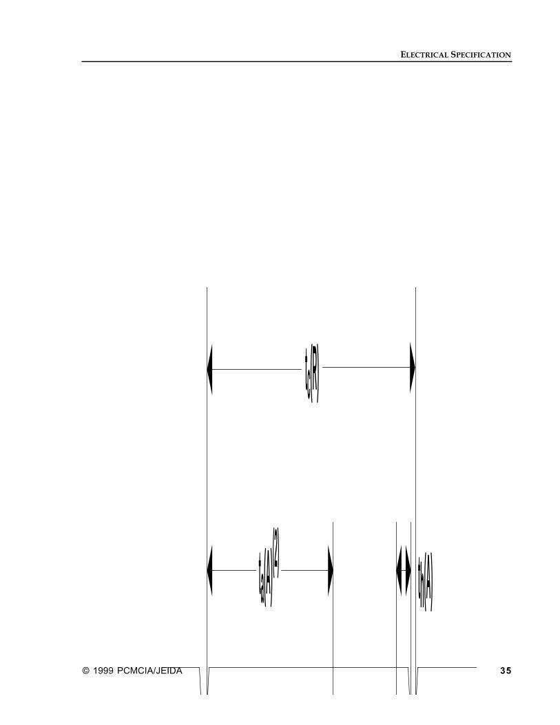
ELECTRICAL SPECIFICATION
© 1999 PCMCIA/JEIDA 35
ta(A)(2)
tc(R)
th(A)

16-BIT PC CARD ELECTRICAL INTERFACE
36 ©1999 PCMCIA/JEIDA
1. Shaded areas may be high or low.2. Applies to card only when WAIT# is negated by card. However, the host shall always provide at leastthis access time before sampling data.3. Applies only when WAIT# is asserted by card.
Figure 4-2 Read Timing Diagram
CE#
D[15::0](Dout)
NOTE 1 NOTE 1
OE#
DATA INPUT ESTABLISHEDD[15::0](Din)
WE#
WAIT#
A[25::0], REG#
NOTE 2
NOTE 3
NOTE 4NOTE 4
tsu(CE-WEH)
tsu(CE)
tcW
tsu(A-WEH) th(CE)
tw(WE)tsu(A) trec(WE)
tsu(OE-WE)
tv(WT-WE)
tw(WT)
tv(WT)
th(OE-WE)
tsu(D-WEH) th(D)
tdis(OE)tdis(WE)
ten(WE)
ten(OE)
1. Shaded areas may be high or low.2. When the data I/O pin is in the output state, no signals shall be applied to the data pins (D[15::0] by the host system.3. Minimum write pulse width must be met whether or not WAIT# is asserted by card.4. May be high or low for write timing, but restrictions on OE# from previous figures apply.
Figure 4-3 Write Timing Diagram
4.8 DMA FunctionThis section describes DMA transfer cycles for PC Cards and sockets capable of DMA operations.DMA operations are described with respect to system memory access. During a DMA write, data istransferred from PC Card I/O space to system memory. During a DMA read, data is transferredfrom system memory to PC Card I/O space.
Address lines to the PC Card are ignored during DMA operations.
The movement of one byte or word of data during a DMA operation, is termed a bus cycle. Severalbus cycles make up a DMA transaction.

ELECTRICAL SPECIFICATION
© 1999 PCMCIA/JEIDA 37
When a PC Card and socket are configured for DMA operations, the DACK (REG#) signal is usedto distinguish between a DMA cycle and a normal I/O cycle. For a normal I/O cycle, the REG#signal is asserted for the complete bus cycle. For a DMA transfer cycle, the REG# signal is negatedduring the entire DMA bus cycle.
4.8.1 DMA Read Function (Memory Read - I/O Write)A PC Card requests a DMA read operation by asserting DREQ#. The host responds by assertingDACK. The host asserts DACK during the entire DMA bus cycle. The host asserts IOWR# totransfer data. When the DMA transfer is complete, the host asserts TC#(WE#) during the last buscycle of the DMA transaction.
Table 4Ð14 DMA Read (Memory Read - I/O Write)
Function DACK DREQ# 1 CE2# CE1# A[25::0] OE# WE# IORD# IOWR# D[15::8] D[7::0]
Standbymode
X X H H X X X X X X X
Byte Access
(8-bit)
H L H L X H TC# H L X BYTEDATA
WordAccess
H L L L X H TC# H L HIGHBYTE
LOWBYTE
1. PC Cards signal DREQ# using one of the following three (3) pins: SPKR#, INPACK# or IOIS16#.
4.8.2 DMA Read Timing (Memory Read - I/O Write)
td DREQ (DACK)th DREQ (DACK) td DREQ (IOWR)
DREQ#
tsu DA(IOWR) th DA (IOWR)
DACK (REG#)
tsu CE (IOWR) th CE (IOWR)
CE#
tw (IOWR)
IOWR#
td (IOWR) th (IOWR)
D[15::0]
tsu (TC) tw (TC) th (TC)
TC# (WE#)
Figure 4-4 DMA Read Timing Diagram

16-BIT PC CARD ELECTRICAL INTERFACE
38 ©1999 PCMCIA/JEIDA
Table 4Ð15 DMA Read Timing Parameters
Item Symbol IEEE Min Max
DREQ# active to DACK active td DREQ (DACK) 10,000
DREQ# hold from DACK active th DREQ (DACK) 0
DREQ# inactive to IOWR# inactive td DREQ (IOWR) 0
Data setup to IOWR# inactive td(IOWR) 100
Data hold from IOWR# inactive th(IOWR) 30
IOWR# Width tw(IOWR) 165
DACK setup to IOWR# active tsu DA (IOWR) 5
DACK hold from IOWR# inactive th DA (IOWR) 5
CE# setup to IOWR# active tsu CE (IOWR) 5
CE# hold from IOWR# inactive th CE (IOWR) 20
IOWR# active to TC# active tsu (TC) 10
TC# Width tw (TC) 40
TC# inactive to IOWR# inactive th (TC) 10
All timing in ns.
4.8.3 DMA Write Function (I/O Read - Memory Write)A PC Card requests a DMA cycle by asserting DREQ#. If the PC Card is granted the DMA request,the host acknowledges the request by beginning the DMA cycle. DACK is held high by the hostduring the entire DMA bus cycle. The host asserts IORD# to transfer data. When the DMA transferis complete, the host asserts TC#(OE#) during the last bus cycle of the DMA transaction.
Table 4Ð16 DMA Write (I/O Read - Memory Write)
Function DACK DREQ# 1 CE2# CE1# A[25::0] OE# WE# IORD# IOWR# D[15::8] D[7::0]
Standbymode
X X H H X X X X X X X
Byte Access
(8-bit)
H L H L X TC# H L H X BYTEDATA
WordAccess
H L L L X TC# H L H HIGHBYTE
LOWBYTE
1. PC Cards signal DREQ# using one of the following three (3) pins: SPKR#, INPACK# or IOIS16#.

ELECTRICAL SPECIFICATION
© 1999 PCMCIA/JEIDA 39
4.8.4 DMA Write Timing (I/O Read - Memory Write)
td DREQ (DACK)th DREQ (DACK) td DREQ (IORD)
DREQ#
tsu DA(IORD) th DA (IORD)
DACK (REG#)
tsu CE (IORD) th CE (IORD)
CE#
tw (IORD)
IORD#
td (IORD) th (IORD)
D[15::0]
tsu (TC) tw (TC) th (TC)
TC# (OE#)
Figure 4-5 DMA Write Timing Diagram
Table 4Ð17 DMA Write Timing Parameters
Item Symbol IEEE Min Max
DREQ# active to DACK active td DREQ (DACK) 10,000
DREQ# hold from DACK active th DREQ (DACK) 0
DREQ# inactive to IORD# inactive td DREQ (IORD) 0
Data Delay from IORD# active td(IORD) 100
Data hold from IORD# inactive th(IORD) 0
IORD# Width tw(IORD) 165
DACK setup to IORD# active tsu DA (IORD) 5
DACK hold from IORD# inactive th DA (IORD) 5
CE# setup to IORD# active tsu CE (IORD) 5
CE# hold from IORD# inactive th CE (IORD) 20
IORD# active to TC# active tsu (TC) 10
TC# Width tw (TC) 40
TC# inactive to IORD# inactive th (TC) 10
All timing in ns.

16-BIT PC CARD ELECTRICAL INTERFACE
40 ©1999 PCMCIA/JEIDA
4.9 Electrical Interface
4.9.1 Signal InterfaceElectrical specifications must be maintained to ensure data reliability.
The 5 V PC Card logic levels shall be per JEDEC 7. The 3.3 V PC Card logic levels shall be perJEDEC 8-1A. (See Table 4Ð18 PC Card Logic Levels.)
Table 4Ð18 PC Card Logic Levels
DC Levels Host Card
Parameter Conditions Min Max
VIH VCC = 5 V ± 5% 2.4 V VCC + 0.25 V TTL or CMOS
VIL VCC = 5 V ± 5% 0.0 V 0.8 V TTL or CMOS
VOH VCC = 5 V ± 5% 2.8 V (0.9 VCC) 1 VCC TTL or CMOS
VOL VCC = 5 V ± 5% 0.0 V 0.5 V (0.1 VCC) 1 TTL or CMOS
VIH VCC = 3.3 V ± 0.3 V 2.0 V VCC + 0.3 V TTL or CMOS
VIL VCC = 3.3 V ± 0.3 V -0.3 V 0.8 V TTL or CMOS
VOH VCC = 3.3 V ± 0.3 V 2.4 V (VCC - 0.2 V) 1 TTL or CMOS
VOL VCC = 3.3 V ± 0.3 V 0.4 V (0.2 V) 1 TTL or CMOS
Note: All logic levels per JEDEC 7 and 8Ð1A. This table is for reference only.1. For CMOS loads.

ELECTRICAL SPECIFICATION
© 1999 PCMCIA/JEIDA 41
Table 4Ð19 Electrical Interface
Item Signal Card Host Card Output Format
Control Signal CE1#CE2#REG#IORD#IOWR#
pull-up to VCC R _ 10 KΩ and mustbe sufficient to keep inputs inactivewhen the pins are not connected atthe host. 3
OE#WE#
pull-up to VCC R _ 10 KΩ *3
RESET pull-up to VCC R _ 100 KΩ *3
Status Signal READYINPACK#WAIT#WP
pull-up to VCC
R _ 10 KΩ 4
Address A[25::0] pull-down R _ 100 KΩ * 5
Data Bus D[15::0] pull-down R _ 100 KΩ * 2
Card Detect CD[2::1]# connected to GND in the card pull-up to VCC
R _ 10 KΩ
Voltage Sense VS1#VS2#
See Table 4Ð5 Vcc at InitialPower-Up and CIS Read.
pull-up to VCC
10 KΩ ≤ R ≤ 100 KΩ
Battery/Detect BVD[2::1] pull-up 1 asserted or negated
* Resistor is optional.1. BVD2 was not defined in the JEIDA 3.0 release. Systems fully supporting JEIDA release 3 SRAM
cards must pull-up pin 62 (BVD2) to avoid sensing their batteries as "Low".2. Data Signals: The host and each card shall present a load no larger than 50 pF at a DC current 450 µA
low state and 150 µA high state. The host and each card shall be able to drive at least the following loadwhile meeting all AC timing requirements: 100 pF with DC current 1.6 mA low state and 300 µA highstate. This permits the host to wire two sockets in parallel without derating the card access speeds.
3. Control Signals: Each card shall present a load to the socket no larger than 50 pF at a DC current of 700µA low state and 150 µA high state, including pull-up resistor. The socket shall be able to drive at leastthe following load while meeting all AC timing requirements: (the number of sockets wired in parallel)multiplied by (50 pF with DC current 700 µA low state and 150 µA high state per socket).
4. Status Signals: The socket shall present a load to the card no larger than 50 pF at a DC current of 400µA low state and 100 µA high state, including pull-up resistor. The card shall be able to drive at leastthe following load while meeting all AC timing requirements: 50 pF at a DC current of 400 µA low stateand 100 µA high state.
5. Address Signals: Each card shall present a load of no more than 100 pF at a DC current of 450A µA lowstate and 150 µA high state. The host shall be able to drive at least the following load while meeting allAC timing requirements: (the number of sockets wired in parallel) multiplied by ( 100 pF with DCcurrent 450 µA low state and 150 µA high state per socket).
4.9.2 Memory Address DecodingThe 26 address signals at the PC Card connector can directly address only 64 MBytes of memory.However, a set of Function Configuration Registers (consisting of four 16-bit Address ExtensionRegisters or the Configuration Option Register) provides the means for an extended PC Cardmemory space containing as many as 242 PC Card Common Memory locations.
The PC Card's external address bus is comprised of A[25::0] with A0 being the LSB and A25 theMSB. Address bit A0 is ignored when the card is asserted in word access mode.
In the case of SRAM without Attribute Memory, address decoding is required as follows:
1. Minimum memory unit is 16 KBytes
2. Memory address starts from 00H
3. Memory units exist continuously.

16-BIT PC CARD ELECTRICAL INTERFACE
42 ©1999 PCMCIA/JEIDA
4.9.2.1 Function Configuration Registers Address Decoding
PC Cards that can be configured by the system, including cards which support I/O and those whichexceed nominal system requirements, contain Function Configuration registers located in theAttribute Memory space. The Function Configuration registers are a set of numbered, standardized,8-bit registers. These registers are addressed at consecutive even-byte addresses starting at the BaseAddress indicated in the Configuration Tuple. Whether a Function Configuration register numberN is present on the card or not, the location of the register is always given by: Base Address + 2 * N.(See also 4.14 Function Configuration and 4.15 Card Configuration.)
4.9.3 I/O Address Space DecodingDuring I/O operations, the I/O address spaces of each PC Card may be either Independent orOverlapping. An Independent I/O address window is a portion of the system's I/O space which isassigned solely to a single PC Card and not shared with any other system resource. Each systemmust be able to allocate to each card an independent I/O address window of at least 8 bytes ofcontiguous address space. The window must begin exactly on an 8-byte boundary. An OverlappingI/O address window is a portion of the system's I/O space which is assigned to any combination ofPC Cards and other system resources. When the Overlapping window method is used by the card,the card responds to only a limited number of the I/O addresses in the window. Also with thismethod, the card may permit the system to choose from a selection of addresses to which the cardcan respond.
During a card reset, and immediately following a card reset, a card will not respond to any I/Oread or I/O write cycles until it has been configured.
PC Cards which implement I/O functions may use either an Independent or Overlapping Windowor permit selecting between the two methods. The types of I/O address decoding performed by thecard, as well as the specific range of addresses to which the card will respond (in Overlapping I/OWindow mode), are described in the Card Configuration Table located within the Card InformationStructure. To select a particular card configuration, the system writes the index number of one tableentry into the Function Configuration Index field of the Configuration Option register. (See also 4.15Card Configuration, the Card Services Specification and the Metaformat Specification.)
In order to be able to accommodate cards which require a higher number of I/O ports, such asLAN, VGA, multi-function cards and game cards, it is recommended that the system reserve 128contiguous bytes of its I/O space.
4.9.3.1 Independent I/O Address Window
Independent I/O Address windows for PC Cards provide a straightforward mechanism for I/Ospace allocation among PC Cards and other system resources installed in the system. The methodcan be applied to systems which permit I/O drivers to determine the card's I/O port assignment atexecution time.
For each PC Card socket, the system must reserve a minimum of 8 contiguous bytes of its I/Oaddress space starting at a Base Address with A0 through A2 all zero.
Note: This should not be interpreted as preventing a system from actuallyallocating a smaller or discontiguous space to a particular I/O card whoseI/O space requires such configuration.
The location of the Independent I/O Address Window for each PC Card socket may be fixedpermanently, or may be allocated when an I/O card is detected in the socket. The system mustinclude a software method permitting driver software (or application software, if I/O is permittedfrom applications) to determine a card's I/O space Base Address.
ELECTRICAL SPECIFICATION
© 1999 PCMCIA/JEIDA 43
Cards which use the Independent I/O Address Window need decode only enough address lines todistinguish among the I/O ports actually implemented on the card. When two identical cards areinstalled in the system, they automatically reside at different addresses. They rely upon the systemto provide sufficient address decoding to prevent conflicts with other installed devices, and may belocated anywhere in the I/O space of the system.
An example of this concept is used in the EISA bus. Each EISA card slot is uniquely assignedthe first 256 bytes of a corresponding 1 KByte of I/O space.
4.9.3.2 Overlapping I/O Address Window
The Overlapping I/O Address Window is provided for those systems whose I/O drivers have theirI/O addresses bound before execution time. This includes both systems for which execution timebinding is not possible, and those having existing drivers which do not take advantage of executiontime binding of I/O addresses.
The system assigns the same block(s) of its I/O space to each PC Card using the Overlapping I/OAddress Window. Other resources in the system may also use portions of the block. Each card andsystem resource is responsible for decoding addresses within the block and responding to I/O onlywithin a unique subset of those addresses. This mechanism relies on the cards and system resourceshaving non-overlapping subsets of addresses to which they respond.
When each PC Card is installed in a system that uses an Overlapping I/O Address Window, theaddresses used by the card must be compared with the addresses used by other installed PC Cards,and the addresses used by other system resources. If the addresses conflict, the new card may begracefully rejected by the system.
A PC Card may allow operation at several alternative sets of addresses. The host selects the desiredalternative from the Card Configuration Table and informs the card by writing the configurationentry of the selected entry to the Function Configuration registers. (See also 4.15 CardConfiguration.)
A desktop personal computer example of Overlapping I/O Address Windows occurs in bothISA and EISA bus-based computers. In these systems all expansion slots are selected during I/Oaccesses to the last 768 bytes of each 1 KByte of I/O space. The expansion cards individuallydetermine to which addresses within that range they will respond. The specific set of addressesis often set by configuration switches, or jumpers, on the expansion card. A service technician isresponsible for ensuring, during installation, that no address conflicts will occur.

16-BIT PC CARD ELECTRICAL INTERFACE
44 ©1999 PCMCIA/JEIDA
4.10 Card DetectPC Cards provide a means of allowing the system to detect card insertion and removal. Signal linesCD[2::1]# are connected to GND in the card. A pull-up resistor must be connected to CD[2::1]# onthe system side.
Vcc
A
Vcc
B
CD1#
CD2#
Host System PC Card
R ≥ 10K Ω
R ≥ 10K Ω
Figure 4-6 Card Detect
4.11 Battery Voltage DetectIt is critical for the system's data integrity to be able to determine the status of the on-card battery.The card provides two status signals for this purpose: BVD[2::1]. A Memory card contains one ortwo voltage comparators and one or two reference voltages. A Memory card compares the batteryvoltage with the reference voltages. Battery status is expressed on 2 digital signal lines, BVD[2::1].If signal BVD2 is not supported, it is held to VCC through a pull-up resistor on the card.
Table 4Ð20 Battery Voltage Detect
BVD1 BVD2 1 COMMENT
H H Battery Operational
H L Battery needs to be replaced.
L H Battery is not providing operational voltage.
L L Battery is not providing operational voltage.
1 If BVD2 is not supported, BVD2 is held to VCC and only one reference voltage is required.

ELECTRICAL SPECIFICATION
© 1999 PCMCIA/JEIDA 45
4.12 Power-up and Power-down
4.12.1 Power-up/Power-down TimingTo retain data in an SRAM Card during power-up or power-down cycles, and to permit peripheralcards to perform power-up initialization, a timing specification is defined as follows.
Table 4Ð21 Power-up/Power-down Timing
Value
Item Symbol Condition Min Max Unit
Card Enable signal level 1 Vi (CE) 0 V ≤ VCC < 2.0 V 0 ViMAX V
2.0 V ≤ VCC < VIH VCC-0.1 ViMAX
VIH ≤ VCC VIH ViMAX
Card Enable Setup Time tsu (VCC) 20 ms
RESET Setup Time tsu (RESET) 20 ms
Card Enable Recover Time trec (VCC) 0.001 ms
VCC Rising Time 2 tpr 10% Ñ> 90% of VCC 0.1 100 ms
VCC Falling Time 2 tpf 90% of VCC Ñ> 10% 3.0 300 ms
RESET Width tw (RESET) 10 us
th (Hi-z RESET) 1 ms
ts (Hi-z RESET) 0 ms
Off time when changing VCC
leveltoff 100 ms
Off level when changing VCC
levelVoff 0.8 V
1. ViMAX means Absolute Maximum Voltage for Input in the period of 0 V ≤ VCC < 2.0 V, Vi (CE) is only 0V ~ ViMAX
2. The tpr and tpf are defined as "linear waveform" in the period of 10% to 90% or vice-versa, Even if thewave form is not "linear waveform", its rising and falling time must be meet this specification.
Peak current at start-up (in-rush current) is determined by ramp time and card capacitance. Sincepeak current is host platform design specific, the design can be optimized within the range definedin Table 4Ð21 Power-up/Power-down Timing for the capability of the platform. Host platforms thatsupport the full range of PC Cards shall assume a 150 µF maximum capacitance before host access(see Section 4.12.2 Average Current During Card Configuration).
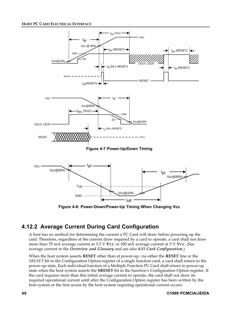
16-BIT PC CARD ELECTRICAL INTERFACE
46 ©1999 PCMCIA/JEIDA
2V
VIH
Vcc
Vcc @ 90%
tpr
tsu (RESET)
2V
VIHtrec (Vcc)
tpfVcc
CE1#, CE2#
RESET
Hi-z
th (Hi-z RESET)
tsu (Vcc)
tw (RESET)
CE1#, CE2#
tsu (RESET)
Hi-z
ts (Hi-z RESET)
tw(RESET)
Vcc@10%
Vcc@10%
Vcc@90%
RESET
Figure 4-7 Power-Up/Down Timing
tpr
Vcc
Vcc@10%
Vcc@90%
GND
Voff
tpf
Vcc@90%
toff
Figure 4-8: Power-Down/Power-Up Timing When Changing Vcc
4.12.2 Average Current During Card ConfigurationA host has no method for determining the current a PC Card will draw before powering up thecard. Therefore, regardless of the current draw required by a card to operate, a card shall not drawmore than 70 mA average current at 3.3 V VCC or 100 mA average current at 5 V VCC. (Seeaverage current in the Overview and Glossary and see also 4.15 Card Configuration.)
When the host system asserts RESET other than at power-up, via either the RESET line or theSRESET bit in the Configuration Option register of a single function card, a card shall return to thepower-up state. Each individual function of a Multiple Function PC Card shall return to power-upstate when the host system asserts the SRESET bit in the functionÕs Configuration Option register. Ifthe card requires more than this initial average current to operate, the card shall not draw itsrequired operational current until after the Configuration Option register has been written by thehost system or the first access by the host system requiring operational current occurs.

ELECTRICAL SPECIFICATION
© 1999 PCMCIA/JEIDA 47
4.12.3 Data RetentionThis specification does not guarantee data retention in memory cards that conform to it. Theconditions in the preceding tables indicate the minimum requirements to ensure data retention. PCCard and system vendors may have to negotiate with each other to determine the detailed methodof guaranteeing data retention for specific memory card models.
4.12.4 SupplementDuring card insertion or removal, with power active, the PC Card data retention capability willdepend on the individual memory card model, the manufacturer's environmental specifications,and other conditions. Therefore, data retention during card insertion or removal when under poweris implementation dependent.
To prevent the situation wherein the PC Card is inadvertently powered while the socket power isOFF, the following requirements shall be fulfilled:
1. When a socketÕs VCC power is switched OFF while a card is in the socket, all socket to cardsignals for that socket shall be less than the voltage presented on the VCC pins on the socketplus +0.3 V at all times.
2. All pull-up resisters on the socket signals except VS[2::1]#, and CD[2::1]# shall be connected toswitched VCC and shall not be active when the socket is powered OFF.
3. The PC Card shall not drive any signals from any other, non-VCC, voltage source (e.g. backupbattery) when the PC Card is powered OFF. (This is a concern primarily in the case ofBVD[2::1] signals tied directly to an SRAM backup battery.)
4.13 I/O FunctionThis section describes the operation and configuration of I/O cards inserted into a PC Card socket.
4.13.1 I/O Transfer FunctionThis section describes the operation of I/O transfer cycles (Input and Output Instructions) on I/Ocards.
4.13.2 I/O Input Function for I/O CardsI/O input transfers from I/O cards may be either 8-bit or 16-bit.
When a 16-bit transfer is attempted from a 16-bit port, the signal IOIS16# must be asserted by theI/O card. Otherwise, the IOIS16# signal must be negated. When a 16-bit transfer is attempted, andthe IOIS16# signal is not asserted by the card, the system generates a pair of 8-bit references toaccess the word's even byte and odd byte.
An I/O card may extend the length of an input cycle by asserting the WAIT# signal at the start ofthe cycle.
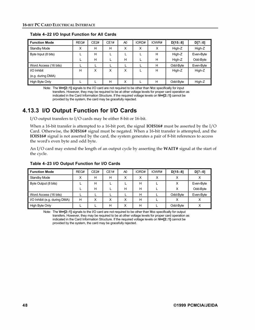
16-BIT PC CARD ELECTRICAL INTERFACE
48 ©1999 PCMCIA/JEIDA
Table 4Ð22 I/O Input Function for All Cards
Function Mode REG# CE2# CE1# A0 IORD# IOWR# D[15::8] D[7::0]
Standby Mode X H H X X X High-Z High-Z
Byte Input (8 bits) L
L
H
H
L
L
L
H
L
L
H
H
High-Z
High-Z
Even-Byte
Odd-Byte
Word Access (16 bits) L L L L L H Odd-Byte Even-Byte
I/O Inhibit
(e.g. during DMA)
H X X X L H High-Z High-Z
High Byte Only L L H X L H Odd-Byte High-Z
Note: The VPP[2::1] signals to the I/O card are not required to be other than VCC specifically for inputtransfers. However, they may be required to be at other voltage levels for proper card operation asindicated in the Card Information Structure. If the required voltage levels on VPP[2::1] cannot beprovided by the system, the card may be gracefully rejected.
4.13.3 I/O Output Function for I/O CardsI/O output transfers to I/O cards may be either 8-bit or 16-bit.
When a 16-bit transfer is attempted to a 16-bit port, the signal IOIS16# must be asserted by the I/OCard. Otherwise, the IOIS16# signal must be negated. When a 16-bit transfer is attempted, and theIOIS16# signal is not asserted by the card, the system generates a pair of 8-bit references to accessthe word's even byte and odd byte.
An I/O card may extend the length of an output cycle by asserting the WAIT# signal at the start ofthe cycle.
Table 4Ð23 I/O Output Function for I/O Cards
Function Mode REG# CE2# CE1# A0 IORD# IOWR# D[15::8] D[7::0]
Standby Mode X H H X X X X X
Byte Output (8 bits) L
L
H
H
L
L
L
H
H
H
L
L
X
X
Even-Byte
Odd-Byte
Word Access (16 bits) L L L L H L Odd-Byte Even-Byte
I/O Inhibit (e.g. during DMA) H X X X H L X X
High Byte Only L L H X H L Odd-Byte X
Note: The VPP[2::1] signals to the I/O card are not required to be other than VCC specifically for outputtransfers. However, they may be required to be at other voltage levels for proper card operation asindicated in the Card Information Structure. If the required voltage levels on VPP[2::1] cannot beprovided by the system, the card may be gracefully rejected.

ELECTRICAL SPECIFICATION
© 1999 PCMCIA/JEIDA 49
4.13.4 I/O Read (Input) Timing Specification
A[25::0]
REG#
CE#
IORD#
INPACK#
IOIS16#
WAIT#
D[15::0]
tsu REG (IORD)
tsu CE (IORD)
th REG (IORD)
th CE(IORD)
tw (IORD)
tsu A (IORD)
th A (IORD)
tdf INPACK (IORD)
tdr INPACK(ADR)
tdf IOIS16 (ADR)
tdr IOIS16(ADR)
tdf WT (IORD) tw (WT)
tdr(WT)td (IORD)
th (IORD)
All timings are measured at the PC Card.Skews and delays from the host system driver/receiver to the PC Card must be accounted for by thesystem design.Minimum time for WAIT# negated to IORD# negated is 0 ns, but minimum IORD# width must still bemet.D[15::0] signifies data provided by the PC Card to the host system.
Figure 4-9 I/O Read Timing

16-BIT PC CARD ELECTRICAL INTERFACE
50 ©1999 PCMCIA/JEIDA
Table 4Ð24 I/O Read(Input) Timing Specification for All I/O Cards
Item Symbol IEEE Symbol Min Max
Data Delay after IORD# td (IORD) t IGLQV 100
Data Hold following IORD# th (IORD) t IGHQX 0
IORD# Width Time tw IORD t IGLIGH 165
Address Setup before IORD# tsu A (IORD) t AVIGL 70
Address Hold following IORD# th A (IORD) t IGHAX 20
CE# Setup before IORD# tsu CE (IORD) t ELIGL 5
CE# Hold following IORD# th CE (IORD) t IGHEH 20
REG# Setup before IORD# tsu REG (IORD) t RGLIGL 5
REG# Hold following IORD# th REG (IORD) t IGHRGH 0
INPACK# Delay Falling from IORD# tdf INPACK (IORD) t IGLIAL 0 45
INPACK# Delay Rising from IORD# tdr INPACK (IORD) t IGHIAH 45
IOIS16# Delay Falling from Address tdf IOIS16 (ADR) t AVISL 35
IOIS16# Delay Rising from Address tdr IOIS16 (ADR) t AVISH 35
WAIT# Delay Falling from IORD# tdfWT (IORD) t IGLWTL 35
Data Delay from WAIT# Rising tdr(WT) t WTHQV 0
WAIT# Width Time tw (WT) t WTLWTH 12,000
All timing in ns.The maximum load on WAIT#, INPACK# and IOIS16# are 1 LSTTL with 50 pF total load.

ELECTRICAL SPECIFICATION
© 1999 PCMCIA/JEIDA 51
4.13.5 I/O Write (Output) Timing Specification
A[25::0]
REG#
CE#
IOWR#
IOIS16#
WAIT#
D[15::0]
tsu REG (IOWR)
tsu CE (IOWR)
th REG (IOWR)
th CE(IOWR)
tw (IOWR)
tsu A (IOWR)
th A (IOWR)
tdf IOIS16 (ADR)
tdr IOIS16(ADR)
tdf WT (IOWR)
tw (WT)
tdr IOWR (WT)
th (IOWR)
tsu (IOWR)
All timings are measured at the PC Card.Skews and delays from the host system driver/receiver to the PC Card must be accounted for by thesystem design.Minimum time for WAIT# negated to IORD# negated is 0 ns, but minimum IOWR# timing must still bemet.D[15::0] signifies data provided by the host system to the PC Card.
Figure 4-10 I/O Write Timing

16-BIT PC CARD ELECTRICAL INTERFACE
52 ©1999 PCMCIA/JEIDA
Table 4Ð25 I/O Write(Output) Timing Specification for All I/O Cards
Item Symbol IEEE Symbol Min Max
Data Setup before IOWR# tsu (IOWR) t DVIWL 60
Data Hold following IOWR# th (IOWR) t IWHDX 30
IOWR# Width Time tw IOWR t IWLIWH 165
Address Setup before IOWR# tsu A (IOWR) t AVIWL 70
Address Hold following IOWR# th A (IOWR) t IWHAX 20
CE# Setup before IOWR# tsu CE (IOWR) t ELIWL 5
CE# Hold following IOWR# th CE (IOWR) t IWHEH 20
REG# Setup before IOWR# tsu REG (IOWR) t RGLIWL 5
REG# Hold following IOWR# th REG (IOWR) t IWHRGH 0
IOIS16# Delay Falling from Address tdf IOIS16 (ADR) t AVISL 35
IOIS16# Delay Rising from Address tdr IOIS16 (ADR) t AVISH 35
WAIT# Delay Falling from IOWR# tdf WT (IOWR) t IWLWTL 35
WAIT# Width Time tw (WT) t WTLWTH 12,000
IOWR# high from WAIT# High tdr IOWR (WT) t WTHIWH 0
All timing in ns.The maximum load on WAIT#, INPACK# and IOIS16# are 1 LSTTL with 50 pF total load.
4.14 Function Configuration
4.14.1 OverviewThe characteristics of some 16-bit PC Cards are configurable. Such PC Cards use FunctionConfiguration registers to control their characteristics and return status. All Function Configurationregisters shall be read/write and one byte wide. All such registers shall be located on even byteaddresses to ensure single cycle access by both eight (8) and sixteen (16) bit host systems.
4.14.2 Single Function PC CardsSingle Function PC Cards shall have a single configuration tuple describing a single set of FunctionConfiguration registers. (See the Metaformat Specification.) All PC Card configuration shall beperformed using this set of Function Configuration registers.
4.14.3 Multiple Function PC CardsMultiple Function PC Cards shall have a separate set of Configuration registers for each function onthe card. Multiple Function PC Cards shall use a combination of a global CIS common to allfunctions on the card and a separate function-specific CIS specific to each function on the card. Theglobal CIS describes features that are common to all functions on the card. Each function-specific CISdescribes features specific to a particular function on the PC Card. A CISTPL_LONGLINK_MFCtuple in the global CIS describes the location of a function-specific CIS for each function on the PCCard. (See the Metaformat Specification.)

ELECTRICAL SPECIFICATION
© 1999 PCMCIA/JEIDA 53
Note: A CISTPL_FUNCID with a TPLFID_FUNCTION field reset to zero (0) shallnot be placed in the CIS of a Multiple Function PC Card. This tuple isreserved for vendor-specific multiple function PC Cards that do not followthe multiple function PC Card definitions in the Standard.
4.14.4 Function Configuration Registers (FCRs)This section describes a PC Card's Function Configuration registers. These registers allow the host toconfigure the function(s) provided by a PC Card. Configurable PC Cards shall implement aConfiguration Option register for each function on the card. Memory cards with more than 64Mbytes of memory must implement either the Configuration Option register or a number ofAddress Extension Registers, with the exact register(s) denoted by the configuration informationprovided by the CISTPL_EXTDEVICE tuple (described in the Metaformat Specification). All otherFunction Configuration registers are optional.
Table 4Ð26 Function Configuration Registers
Offset 7 6 5 4 3 2 1 0
0 Configuration Option Register
SRESET LevIREQ Function Configuration Index / Common Memory Address Extension
2 Configuration and Status Register
Changed SigChg IOIs8 RFU Audio PwrDwn Intr IntrAck
4 Pin Replacement Register
CBVD1 CBVD2 CREADY CWProt RBVD1 RBVD2 RREADY RWProt
6 Socket and Copy Register
RFU Copy Number Socket Number
8 Extended Status Register
Event3 Event2 Event1 Req Attn Enable3 Enable2 Enable1 Req AttnEnable
10 I/O Base 0
12 I/O Base 1
14 I/O Base 2
16 I/O Base 3
18 I/O Limit
20 Power Management Support Register
RFU(0) RFU(0) RFU(0) RFU(0) StateRestored
Begin/DoneState
Operation
Save/Restore
State
Stored StateExists
22 Address Extension Register 0 Low
24 Address Extension Register 0 High
26 Address Extension Register 1 Low
28 Address Extension Register 1 High
30 Address Extension Register 2 Low
32 Address Extension Register 2 High
34 Address Extension Register 3 Low
36 Address Extension Register 3 High

16-BIT PC CARD ELECTRICAL INTERFACE
54 ©1999 PCMCIA/JEIDA
4.15 Card ConfigurationEach configurable PC Card is identified by a Card Configuration Table in the card's CardInformation Structure. These cards must have one or more of a set of Function Configurationregisters which are used to control the configurable characteristics of the card. The configurablecharacteristics include the electrical interface, I/O address space, interrupt request, and powerrequirements of the card.
All of the Function Configuration registers shall be both readable and writable. The registers areeach one byte in size and located only on even-byte addresses to ensure their single cycle access byboth 8-bit and 16-bit systems.
These registers also provide a method for accessing some status information about a card. Theinformation may be used to arbitrate between multiple-interrupt sources on the same interruptrequest level. It may also be used to access status information which appears on pins 16, 33, 62 and63 (READY, WP, and BVD[2::1]) in Memory Only cards.
At every moment, the effect of a particular combination of configuration values shall be dependentonly on the current values in the registers. Card function configuration shall be independent of themanner in which the values were loaded into the registers.
With the exception of the transient states occurring during a socket/card configuration and thepotential initialization of a Socket and Copy register, the order of initializing the registers is notrestricted. (See 4.15.4 Socket and Copy Register.) Cards shall respond appropriately regardless ofthe order in which their registers have been initialized.
Regardless of the current draw required by a card to operate, a card shall not draw more than 70mA average current at 3.3 V VCC or 100 mA average current at 5 V VCC after being initiallypowered-up. (See average current in the Overview and Glossary and see also 4.12.2 AverageCurrent During Card Configuration.) While in this Power-up state, the card shall allow CIS to beread and Configuration registers to be accessed. If the card requires more than this initial averagecurrent to operate, the card shall not draw its required operational current until after theConfiguration Option register has been written by the host or the first access to other than CIS orConfiguration registers by the host requiring operational current occurs.
Table 4Ð27 Card Memory Spaces
CE1# REG# OE# WE# Address Offset A0 Selected Register or Space
H X X X X X Standby
L H L H X X Common Memory Read
L H H L X X Common Memory Write
L L L H X L CIS or Configuration Register Read
L L H L X L CIS or Configuration Register Write
L L X X X H Invalid Access

ELECTRICAL SPECIFICATION
© 1999 PCMCIA/JEIDA 55
Table 4Ð28 Function Configuration Registers
CE1# REG# OE# WE# Address Offset 1 A0 Selected Register RegisterNum
L L L H NNNN0H L Configuration Option Register Read 0
L L H L NNNN0H L Configuration Option Register Write 0
L L L H NNNN2H L Configuration and Status Register Read 1
L L H L NNNN2H L Configuration and Status Register Write 1
L L L H NNNN4H L Pin Replacement Register Read 2
L L H L NNNN4H L Pin Replacement Register Write 2
L L L H NNNN6H L Socket and Copy Register Read 3
L L H L NNNN6H L Socket and Copy Register Write 3
L L L H NNNN8H L Extended Status Register Read 4
L L H L NNNN8H L Extended Status Register Write 4
L L L H NNNN0H + 14H L Power Management Register Read 10
L L H L NNNN0H + 14H L Power Management Register Write 10
L L L H NNNN0H + 16H L Address Extension Register 0 Low Read 11
L L H L NNNN0H + 16H L Address Extension Register 0 Low Write 11
L L L H NNNN0H + 18H L Address Extension Register 0 High Read 12
L L H L NNNN0H + 18H L Address Extension Register 0 High Write 12
L L L H NNNN0H + 1AH L Address Extension Register 1 Low Read 13
L L H L NNNN0H + 1AH L Address Extension Register 1 Low Write 13
L L L H NNNN0H + 1CH L Address Extension Register 1 High Read 14
L L H L NNNN0H + 1CH L Address Extension Register 1 High Write 14
L L L H NNNN0H + 1EH L Address Extension Register 2 Low Read 15
L L H L NNNN0H + 1EH L Address Extension Register 2 Low Write 15
L L L H NNNN0H + 20H L Address Extension Register 2 High Read 16
L L H L NNNN0H + 20H L Address Extension Register 2 High Write 16
L L L H NNNN0H + 22H L Address Extension Register 3 Low Read 17
L L H L NNNN0H + 22H L Address Extension Register 3 Low Write 17
L L L H NNNN0H + 24H L Address Extension Register 3 High Read 18
L L H L NNNN0H + 24H L Address Extension Register 3 High Write 18
1. NNNN0H is the Configuration registers Base Address specified in the TPCC_RADR field of theConfiguration Tuple. (See the Metaformat Specification.)
4.15.1 Configuration Option RegisterThe Configuration Option register is used to configure the card, provide an address extension toselect a 64 MByte page of Common Memory, and to issue a soft reset to the card. The register is aread/write register which contains three fields. The Configuration Option register must beimplemented in all configurable cards.
The Configuration Option register is required on PC Cards using the I/O interface and is optionalon PC Cards using the memory interface. The register configures a function on a PC Card and maybe used to issue a soft reset to the function or set the interrupt mode (Level or Pulse) used by thefunction.

16-BIT PC CARD ELECTRICAL INTERFACE
56 ©1999 PCMCIA/JEIDA
For memory PC Cards where it is not necessary to configure a function on the PC Card, theConfiguration Option registerÕs Common Memory Address Extension field can serve to provide sixaddress extension bits. The six address extension bits when combined with the PC Cards 26 addresssignals (A[25::0]), would allow for the addressing of as much as 4 Gigabytes of Common Memoryfor PC Cards employing a 64 MByte paging architecture. The CORÕs Common Memory AddressExtension field would select the various 64 MByte pages while the A[25::0] signals would select aspecific memory location within a selected page.
The Configuration Option register is organized as follows:
Table 4Ð29 Configuration Option Register
D7 D6 D5 D4 D3 D2 D1 D0
SRESET LevIREQ Function Configuration Index / Common Memory Address Extension
Field Type Description
SRESET R/W If the host sets this field to one (1), the PC Card shall place the function in reset state. This isequivalent to the host asserting RESET, except this field is not reset to zero (0) as it is when the hostasserts RESET. When the host returns this field to zero (0), the function shall enter the sameunconfigured, reset state as the card does following a power-up and hardware reset.
LevIREQ R/W If a PC card is using the I/O interface and this field is set to one (1), the PC Card shall generate LevelMode interrupts.
If a PC card is using the I/O interface and this field is set to zero (0), the PC Card shall generate PulseMode interrupts, if they are supported by the card. A PC Card indicates it supports Pulse Modeinterrupts in the Interrupt Request Description Structure of a Function Configuration Table Entry Tuple.
If a PC Card has multiple I/O functions, all functions using interrupts on the PC Card shall use thesame interrupt mode. This must be enforced by host software.
If a PC Card is not using the I/O interface, this field is undefined.
FunctionConfiguration
Index
R/W When the host system sets this field to the value of the Configuration Entry Number field of aConfiguration Table Entry Tuple the function shall enter the configuration described by that tuple. Thisfield shall be reset to zero (0) by the PC Card when the host sets the SRESET field to one (1) or thehost asserts RESET.
If this field is set to zero (0) explicitly by the host or implicitly by SRESET or RESET, the PC Cardshall use the Memory Only interface and I/O cycles from the host shall be ignored by the card.
When a PC Card configuration requires an interface other than memory (including CustomInterfaces), the socket controller must be programmed for that interface before the ConfigurationOption Register is set. The Card Information Structure (CIS) must be readable as specified in theMetaformat Specification no matter what interface is in use.
On multiple function PC Cards, bits in this field enable the following functionality:
Bit 0 Enable Function - If this bit is reset to zero (0), the function is disabled. If this bit is set to one(1), the function is enabled.
Bit 1 Enable Base and Limit Registers - If this bit is reset to zero (0) and Bit 0 is set to one (1), allI/O addresses on the host system are passed to the function. If this is set to one (1) and Bit 0is set to one (1), only I/O addresses that are qualified by the Base and Limit registers arepassed to the function. If Bit 0 is reset to zero (0), this bit is undefined.
Bit 2 Enable IREQ# routing - If this bit is reset to zero (0) and Bit 0 is set to one (1), this functionshall not generate interrupt requests on the PC Card's IREQ# line. If this is set to one (1) andBit 0 is set to one (1), this function shall generate interrupt requests on the PC Card's IREQ#line. If Bit 0 is reset to zero (0), this bit is undefined.
Bit 3 .. 5 are reserved for vendor implementation.
Common MemoryAddress Extension
R/W For a memory card with > 64 MBytes of Common Memory and using 64 MByte paging this field canbe used to provide six address extension bits which select a 64 MByte page within a CommonMemory space as large as 4 Gigabytes. The selection of the Common Memory Address Extensionfield option for use with 64 MByte paging as well as the exact size of Common Memory is specified bythe CISTPL_EXTDEVICE tuple.

ELECTRICAL SPECIFICATION
© 1999 PCMCIA/JEIDA 57
The timing of the Soft Reset must meet the same constraints as the timing of hardware reset. Toclear the Soft Reset Bit (1->0) in the Configuration Option register, the host shall write a 00H to theregister. This procedure ensures that the proper final result will occur in the register regardless ofwhether the card treats the write as occurring during the reset (and clears bits 6-0 regardless of thevalues written) or treats the write as occurring at the end of the reset (and allows bits 6-0 to be setaccording to the values written).
After clearing the Soft Reset bit, the host shall follow the same protocol as is used for hardware reset.The host must observe the Ready condition of the READY signal before proceeding in there-initialization of the card. After the Socket and Copy register has been written, the host can writethe Configuration Option register with the desired configuration value.
4.15.2 Configuration and Status RegisterThe Configuration and Status register is an optional register. If present, the register allowsadditional control over a function's configuration and reports status related to the function'sconfiguration.
Table 4Ð30 Configuration and Status Register
D7 D6 D5 D4 D3 D2 D1 D0
Changed SigChg IOIs8 RFU Audio PwrDwn Intr IntrAck

16-BIT PC CARD ELECTRICAL INTERFACE
58 ©1999 PCMCIA/JEIDA
Field Type Description
Changed R/O If a PC Card is using the I/O interface, the function's Pin Replacement register is present and one ormore of the state change signals in the Pin Replacement register are set to one (1), or one Event bitsin the Extended Status register are set (1) and the corresponding Enable bit is set (1), the function shallset this field to one (1).
If a PC Card is not using the I/O interface or the function's Pin Replacement register is not present,this field is undefined and should be ignored.
SigChg R/W This field serves as a gate for STSCHG#.
If a PC Card is using the I/O interface and both the Changed and SigChg fields are set to one (1), thefunction shall assert STSCHG#.
If a PC Card is using the I/O interface and this field is reset to zero (0), the function shall not assertSTSCHG#.
If a PC Card is not using the I/O interface or the function's Pin Replacement register is not present,this field is undefined and should be ignored.
IOIs8 R/W The host sets this field to one (1) when it can provide I/O cycles only with an 8-bit D[7::0] data path.The card is guaranteed that accesses to 16-bit registers will occur as two byte accesses rather thanas a single 16-bit access.
RFU Reserved. Must be zero (0).
Audio R/W This bit is set to one (1) to enable audio information on SPKR# when the card is configured.
PwrDwn R/W When the host sets this field to one (1), the function shall enter a power-down state, if such a stateexists.
While this field is one (1), the host shall not access the function. The host shall return this field to zero(0) before attempting to access the function.
The host shall set this field only if the PC Card is indicating it is ready.
If a PC Card function does not have a power-down state, the function shall ignore this field.
Intr R/O
or
R/W
Interrupt Request/Acknowledge - This field reports whether the function is requesting interruptservicing and may be used to acknowledge the host system is ready to process another interruptrequest from the PC Card.
The function shall set this field to one (1) when it is requesting interrupt service. The function shall setthis field to zero (0) when it is not requesting interrupt service.
Writes to this field are ignored when the IntrAck field of all Configuration and Status Registers on thePC Card are reset to zero (0).
If the host system writes a zero (0) to this field in any Configuration and Status Register on the PCCard when the IntrAck field of any Configuration and Status Register is set to one (1) and any functionon the PC Card is requesting interrupt servicing, the PC Card must create an additional interruptnotification to the host system.
IntrAck R/W Interrupt Acknowledge - This field changes the response characteristics of the Intr field on MultipleFunction PC Cards that have multiple sets of configuration registers. This field is used to enable ahardware/software protocol that permits the PC CardÕs IREQ# signal to be shared by multiplefunctions on the card. Single function PC Cards ignore this field on writes and always return zero (0).
If the IntrAck field of every Configuration and Status Register on a Multiple Function PC Card is resetto zero (0), writes to the Intr field are ignored.
If the IntrAck field of any Configuration and Status Register on a Multiple Function PC Card is set toone (1):
• the host system must acknowledge it is ready to receive additional interrupts from the PC Cardby writing a zero (0) to the Intr field of any Configuration and Status Register after the hostsystem has completed an entire interrupt processing cycle.
• the PC Card must create an additional interrupt notification to the host system when the hostsystem writes a zero (0) to the Intr field in any Configuration and Status Register on the PC Cardand any function on the PC Card enabled for interrupt reporting and sharing is requestinginterrupt service.
Host software must insure the IntrAck field is set to one (1) for all functions sharing the PC CardÕsIREQ# signal using the above described protocol.
The Configuration and Status register must be implemented if the card generates audio, sharesinterrupts or requires other status information available in the register.

ELECTRICAL SPECIFICATION
© 1999 PCMCIA/JEIDA 59
4.15.3 Pin Replacement RegisterThe Pin Replacement register is used to provide the card status information which was provided onpins 16, 33, 62 and 63 in the Memory Only interface.
The register may be read and written, however, when written the lower 4 bits act as mask bits forchanging the corresponding bit of the upper 4 bits.
The upper 4 bits are set when the corresponding bit in the lower 4 bits changes state.
Table 4Ð31 Pin Replacement Register
D7 D6 D5 D4 D3 D2 D1 D0
CBVD1 CBVD2 CREADY CWProt RBVD1 RBVD2 RREADY RWProt
Field Description
CBVD1 This bit is set (1) when the corresponding bit, RBVD1, changes state. This bit may also be written by the host.
CBVD2 This bit is set (1) when the corresponding bit, RBVD2, changes state. This bit may also be written by the host.
CREADY This bit is set to one when the bit RREADY changes state. This bit may also be written by the host.
CWProt This bit is set to one when the bit RWProt changes state. This bit may also be written by the host.
RBVD1 When read, this bit represents the internal state of the Battery Voltage Detect circuits which would be on theBVD1 pin.
When this bit is written as 1 the corresponding CBVD1 bit is also written. When this bit is written as 0, theCBVD1 bit is unaffected.
RBVD2 When read, this bit represents the internal state of the Battery Voltage Detect circuits which would be on theBVD2 pin.
When this bit is written as 1 the corresponding CBVD2 bit is also written. When this bit is written as 0, theCBVD2 bit is unaffected.
RREADY When read, this bit represents the internal state of the READY signal. This bit may be used to determine the stateof READY as that pin has been reallocated for use as Interrupt Request on IO Cards.
When this bit is written as 1 the corresponding "changed" bit is also written. When this bit is written as 0, thecorresponding changed bit is unaffected.
RWProt This bit represents the state of the WP signal. This signal may be used to determine the state of the Write Protectswitch when pin 33 is being used for IOIS16#.
When this bit is written as 1 the corresponding "changed" bit is also written. When this bit is written as 0, thecorresponding changed bit is unaffected.
The Pin Replacement register must be implemented if the card needs to provide information aboutREADY, WP or the BVD[2::1] status when implementing the I/O interface.
4.15.4 Socket and Copy RegisterThis is an optional read/write register which the PC Card may use to distinguish between similarcards installed in a system. This register, if present, is always written by the system before writingthe card's Function Configuration Index field in the Configuration Option register.
Table 4Ð32 Socket and Copy Register Organization
D7 D6 D5 D4 D3 D2 D1 D0
Reserved Copy Number Socket Number

16-BIT PC CARD ELECTRICAL INTERFACE
60 ©1999 PCMCIA/JEIDA
Field Description
Reserved This bit is reserved for future standardization. This bit must be set to zero (0) by software when the register iswritten.
Copy Number PC Cards which indicate in their CIS that they support more than one copy of identically configured cards, shouldhave a copy number (0 to MAX twin cards, MAX = n-1) written back to the Socket and Copy register.
This field indicates to the card that it is the n'th copy of the card installed in the system which is identicallyconfigured. The first card installed receives the value 0. This permits identical cards designed to do so to share acommon set of I/O ports while remaining uniquely identifiable. and consecutively ordered.
Socket Number This field indicates to the PC Card that it is located in the n'th socket. The first socket is numbered 0. Thispermits any cards designed to do so to share a common set of I/O ports while remaining uniquely identifiable.
4.15.5 Extended Status RegisterThis is an optional register that will be located at offset 08H. The register will contain informationabout the changes in the cards status. The Extended Status register bit assignments are definedbelow:
Table 4Ð33 Extended Status Register Organization
D7 D6 D5 D4 D3 D2 D1 D0
Event3 Event2 Event1 Req Attn Enable3 Enable2 Enable1 Req AttnEnable
Field Description
Event3 Reserved for future expansion/definition, must be reset (0)
Event2 Reserved for future expansion/definition, must be reset (0)
Event 1 Reserved for future expansion/definition, must be reset (0)
Req Attn This bit is latched within one(1) ms of an event occurring on the PC Card, (such as the start of each cycle of thering frequency to indicate the presence of ringing on the phone line in the case of a modem card). When this bit isset to a one (1), and the Req Attn Enable bit is set to a one (1), the Changed bit in the Configuration and Statusregister will also be set to a one (1), and if the SigChg bit in the Configuration and Status register has also beenset by the host, then the STSCHG# pin (63) will be asserted. The host writing a one (1) to this bit will reset it tozero (0). Writing a zero (0) to this bit will not have any effect.
Enable3 Reserved for future expansion/definition, must be reset (0)
Enable2 Reserved for future expansion/definition, must be reset (0)
Enable1 Reserved for future expansion/definition, must be reset (0)
Req Attn Enable Setting this bit to a one (1) enables the setting of the Changed bit in the Configuration and Status register when theReq Attn bit is set. When this bit is reset to a zero (0), this feature is disabled. The state of the Req Attn bit is notaffected by the Req Attn Enable bit.
The register may be read or written. The upper 4 bits are latched to a one (1) when thecorresponding event occurs on the PC Card (for example in the case of the Req Attn bit, whenringing occurs on the phone line on a modem card). When one of these upper four bits is latchedand the corresponding enable bit in the lower nibble is also set, the Changed bit in theConfiguration and Status register will be set, and if the SigChg bit in the Configuration and Statusregister is also set, (and the card is configured for I/O mode) then the STSCHG# pin (63) will beasserted. The host writing a one (1) to one of the upper 4 bits will clear that bit. Writing a zero toone of the upper 4 bits will have no effect. The lower four bits will return their current state whenthey are read. All bits of this register are cleared to zero (0) at power-up(VCC), by RESET orSRESET.

ELECTRICAL SPECIFICATION
© 1999 PCMCIA/JEIDA 61
Setting one of the lower 4 bits enables the corresponding upper bit to be OR'ed into the Changed bitin the Configuration and Status register. When these lower bits are cleared, the setting of theChanged bit is disabled for the corresponding event. The state of the upper bits is not affected by thevalue written to the lower bits.
The host will determine the presence of this register by reading the TPCC_RMSK Configurationregister Presence Mask of the Card Configuration Tuple. (See the Metaformat Specification.)
4.15.6 I/O Base Registers (0 .. 3)The I/O Base registers are optional on single function PC Cards. They are required on multiplefunction PC Cards. The I/O Base registers determine the base address of the I/O range used toaccess function specific registers on the PC Card. These registers allow the PC Card's functionspecific registers to be placed anywhere in the host system's I/O address space. The registers arewritten in little-endian order with the least significant byte of the base I/O address written to I/OBase 0.
The number of I/O Base Address registers implemented depends on the number of address linesthe PC Card decodes. For example, if the function on the PC Card only decodes sixteen (16) addresslines, only the first two registers need to be implemented.
Table 4Ð34 I/O Base Registers
Offset D7 D6 D5 D4 D3 D2 D1 D0
10 I/O Base 0
12 I/O Base 1
14 I/O Base 2
16 I/O Base 3
Field Type Description
I/O Base (0 .. 3) R/W Base I/O address used by function on PC Card.
4.15.7 I/O Limit RegisterThe I/O Limit register is an optional register. It is only implemented on PC Cards that use I/O BaseAddress registers. If the function on the PC Card always uses the same number of I/O registers inall configurations, this register may be omitted (even on PC Cards with I/O Base Address registers).
This register specifies the number of address lines used by the function. Each bit in the registerrepresents an I/O address line. This allows two (2) to two hundred and fifty-six (256) I/O ports to beused by a function. If a bit in the register is set to one (1), all bits of lesser significance in the registermust also be set to one (1).
Table 4Ð35 I/O Limit Register
Offset D7 D6 D5 D4 D3 D2 D1 D0
18 I/O Limit

16-BIT PC CARD ELECTRICAL INTERFACE
62 ©1999 PCMCIA/JEIDA
Field Type Description
I/O Limit R/W Bit-mapped register indicating the number of I/O address lines decoded by the function on the PCCard.
4.15.8 Power Management Support RegisterThe Power Management Support Register is used in conjunction with the CISTPL_PWR_MGMNTtuple (see the Metaformat Specification) by host software to preserve the state of a PC Card functionwhen power is removed from a socket and then later power is restored. Before socket power isremoved, the host commands the PC Card function to perform a save state operation by first settingthe Save/Restore state field to one (1) and the Begin/Done State Operation field to one (1). The host shallallow the PC Card function up to the period of time indicated by the PWR_TIME field in theCISTPL_PWR_MGMNT tuple to complete the save state operation before power is removed from thesocket. The PC Card function indicates the operation is complete by clearing the Begin/Done StateOperation field to zero (0). After socket power is restored, the PC Card function restores a saved statewithin the period of time indicated by the PWR_TIME field in the CISTPL_PWR_MGMNT tuplewhen the host clears the Save/Restore state field to zero (0) and sets the Begin/Done State Operationfield to one (1).
Field Description
Stored State Exists When set, indicates the PC Card function has preserved a state within the card that can be restored.
This field is cleared to zero (0) by the PC Card function when the saved state is restored or the function isconfigured.
Save/RestoreState
When commanded by the host to begin a Save/Restore State operation, this field instructs the function to savestate if set to one (1) or restore state if cleared to zero (0).
Begin/Done StateOperation
When set to one (1) by the host, this field commands the function to begin a save or restore state operation. Uponcompleting the save or restore state operation and the function is ready for operation, this field is cleared to zero(0) by the PC Card function.
If the PC Card function has not completed itÕs part of the operation within its specified save/restore time andindicated successful completion by clearing this field, the host shall assume the operation has failed.
State Restored This field is set to one (1) by the PC Card function when a restore state operation is successfully completed.
This field is cleared to zero (0) by the PC Card function when a state is saved or the function is configured.
RFU(0) Reserved, cleared to zero
RFU(0) Reserved, cleared to zero
RFU(0) Reserved, cleared to zero
RFU(0) Reserved, cleared to zero
There are two methods of PC Card function state preservation defined: one method stores stateinformation within the card, the other relies on the host to store the functionÕs state information.
In the first method (when the CISTPL_PWR_MGMNT tuple PWR_METHOD field is 80H), the PCCard function stores state information on the card and indicates that the function has stored a validstate by setting the Stored State Exists field to one (1). The host responsibility is limited to indicatingwhen to save state and when to restore state. Whenever the PC Card function is configured by thehost or a saved configuration state is restored, the function shall clear the Stored State Exists field tozero (0).
In the second method (when the CISTPL_PWR_MGMNT tuple PWR_METHOD field is 00H or 01H)the PC Card function outputs state information to a buffer area on the card during a save stateoperation and restores state information from the buffer area during a restore state operation. The

ELECTRICAL SPECIFICATION
© 1999 PCMCIA/JEIDA 63
host is responsible for storing the contents of the buffer after the PC Card function indicates the savestate operation is complete and before the card is powered down. After re-powering the PC Cardand before starting the functionÕs restore state operation, the host reloads the saved buffer contentsinto the buffer area.
For either method, the PC Card is responsible for restoring the state of the functionÕs internalsincluding the state of the functionÕs Configuration Registers. In a restore sequence, the hostÕsresponsibilities are to restore the state of the socket, verify that the PC Card in the socket has notbeen removed from the socket since state was saved, reload the functionÕs state buffer (only when abuffer method is used), and command the PC Card function to restore its state. When a restore stateoperation is successfully completed the PC Card function shall set the State Restored field to one (1).The last two host steps, reload the PC Card functionÕs state buffer and command the function torestore its state, are repeated for each function on a Multiple Function PC Card.
The PC Card function shall save state when commanded to do so by the host regardless of havingpreviously saved state.
4.15.9 Address Extension RegistersThis optional set of Function Configuration Registers provides a means for a system to access morethan 64 MBytes of Common Memory space on a PC Card. The 26 address signals at the PC Cardconnector can directly address only 64 MBytes of memory. The Address Extension Registers providean address extension which allows the host system to address locations within an extended PC Cardmemory space containing as many as 242 PC Card Common Memory locations with 8-bit registers.(Additionally, as described in Section 4.15.1 Configuration Option Register, the ConfigurationOption Register may be used to provide 6 address extension bits as an alternative to the AddressExtension Registers.)
Eight Function Configuration Register locations in attribute memory have been assigned to theAddress Extension Registers. The Address Extension Register locations are organized in pairs toallow for 4 16-bit Address Extension Registers. However, either one, two or four Address ExtensionRegisters may appear on a PC Card and these registers may be either 8-bit or 16-bit. The highestnumbered (offset) register of a Function Configuration Register pair is the upper byte of theAddress Extension Register.
When four Address Extension Registers are present on the PC Card, the A[23::0] card addresssignals select a byte or word location within a 16 MByte page of memory while one of the fourregisters provides an address extension to select the 16 MByte page. The address extension for thepage is defined in terms of extended address signals, starting with MA24 as the least significant bit.The extended address signals appear in the Address Extension Registers as follows:
Register Offset 7 6 5 4 3 2 1 0
22, 26, 30 & 34 Address Extension Register 0, 1, 2 & 3 Low
MA31 MA30 MA29 MA28 MA27 MA26 MA25 MA24
24, 28, 32 & 36 Address Extension Register 0, 1, 2 & 3 High
MA39 MA38 MA37 MA36 MA35 MA34 MA33 MA32
During a memory cycle the cardÕs A24 and A25 address input signals select which one of the fourAddress Extension Registers provides the extended address signals to memory. The registerselection is defined as follows:

16-BIT PC CARD ELECTRICAL INTERFACE
64 ©1999 PCMCIA/JEIDA
A25 A24 Selected Register
0 0 Address Extension Register 0
0 1 Address Extension Register 1
1 0 Address Extension Register 2
1 1 Address Extension Register 3
When two Address Extension Registers are present on the PC Card, the A[24::0] card addresssignals select a byte or word location within a 32 MByte page of memory while one of the tworegisters provides an address extension to select the 32 MByte page. The address extension for thepage is defined in terms of extended address signals, starting with MA25 as the least significant bit.The extended address signals appear in the Address Extension Registers as follows:
Register Offset 7 6 5 4 3 2 1 0
22 & 26 Address Extension Register 0 & 1 Low
MA32 MA31 MA30 MA29 MA28 MA27 MA26 MA25
24 & 28 Address Extension Register 0 & 1 High
MA40 MA39 MA38 MA37 MA36 MA35 MA34 MA33
During a memory cycle the cardÕs A25 address input signal selects which one of the two AddressExtension Registers provides the extended address signals to memory. The register selection isdefined as follows:
A25 Selected Register
0 Address Extension Register 0
1 Address Extension Register 1
When only one Address Extension Register is present on the PC Card, the A[25::0] card addresssignals select a byte or word location within a 64 MByte page of memory while the register providesan address extension to select the 64 MByte page. The address extension for the page is defined interms of extended address bits, starting with MA26 as the least significant bit. The extended addressbits appear in the Address Extension Register 0 as follows:
Register Offset 7 6 5 4 3 2 1 0
22 Address Extension Register 0 Low
MA33 MA32 MA31 MA30 MA29 MA28 MA27 MA26
24 Address Extension Register 0 High
MA41 MA40 MA39 MA38 MA37 MA36 MA35 MA34
The exact number of Function Configuration Registers supported by a PC Card is specified by theTPCC_RMSK byte of the CISTPL_CONFIG tuple. Thus, a PC CardÕs Card Information Structure(CIS) indicates which Address Extension Registers are present. However, software can alsodetermine used and unused register locations by writing the registers first with a pattern of all 1Õsand then with a pattern of all 0Õs, each time reading the register locations to determine whereregisters actually exist to store the pattern. Unused register bytes are reserved for unused extendedaddress signals and return either all '0' bits or all '1' bits when read. The Address Extension RegisterHigh bytes need be present on a PC Card only for Common Memory spaces requiring more thanthe eight address extension bits provided by a single 8-bit register.

ELECTRICAL SPECIFICATION
© 1999 PCMCIA/JEIDA 65
When an Address Extension Register is provided by a PC Card, the associated Address ExtensionRegister Low byte is always present (as indicated by TPCC_RMSK). However, not all 8 bits of anAddress Extension Register are required to be implemented for address extension. Unused registerbits are reserved for unused extended address signals and return either all 0Õs or all 1Õs when read.
Even though the Address Extension Registers can provide an address extension which addressesbeyond 4 GBytes of Common Memory, the Card Services Specification as of the PC Card StandardRelease 6.1 supports a maximum Common Memory size of 4 GBytes.
Upon card power-up the PC Card initializes its Address Extension Registers to form a contiguous 64MByte area in Common Memory. The contiguous 64 MByte area provides a single 64 MByte area ofmemory which non-extended PC host software (without address extension knowledge) can address.To form the contiguous 64 MByte area, each register is set to the registerÕs number, i.e., AddressExtension Register 0 is set to 0, Address Extension Register 1 is set to 1, Address Extension Register2 is set to 2, and Address Extension Register 3 is set to 3. After the registers have been initialized,the host processor can write a register with the address extension of any page in the cardÕs memoryarray.
4.16 Indirect Access to PC Card MemoryThis optional register set, located in common memory space, enables an indirect access mechanismfor 16-bit PC Cards. (See CISTPL_INDIRECT in the Metaformat Specification.) This mechanismrequires only four (4) address lines to provide access to spaces equivalent to the standard 16-bit PCCard Attribute and Common Memory spaces. All registers may be read or written.
The actual size of any indirect access spaces is determined by the card vendor as it is for standardCommon Memory and Attribute Memory spaces.
Table 4Ð36 Indirect Access Registers
Offset D7 D6 D5 D4 D3 D2 D1 D0
2 Control_lo
Reserved Byte Gran Auto Inc Space
3 Control_hi
Reserved
4 .. 7 Address
8 .. 9 Data

16-BIT PC CARD ELECTRICAL INTERFACE
66 ©1999 PCMCIA/JEIDA
Field Description
Control_hiControl_lo
This sixteen (16) bit register controls read and write accesses through the Data register at the address present inthe Address register.
Space 0 = Indirect Attribute Space 1 = Indirect Common Space
Auto Inc 0 = do not adjust Address when a read or write access is made to Data. 1 = adjust Address according to the Byte Gran setting on each Data access.
Byte Gran This field is ignored when the Auto Inc field is zero (0).
0 = add two (2) to Address following each Data access. 1 = add one (1) to Address following each Data access.
Reserved These register bits are reserved and must be set to zero.
Address This register indicates the current twenty-six (26) bit address that will be used on the next Data access.
Data Reading this sixteen (16) bit register will fetch the sixteen (16) bit value at the indirect address indicated by theSpace setting in the Control register using the current value of Address. If the Space setting indicates indirectAttribute Space, only the even byte data is valid.
Writing a value to this register will present a write operation to card memory at the indirect address indicated bythe Space setting in the Control register and the current value of Address.

ELECTRICAL SPECIFICATION
© 1999 PCMCIA/JEIDA 67
5 . C A R D B U S P C C A R D E L E C T R I C A L
I N T E R F A C E
The CardBus PC Card Interface provides a high performance 32-bit/bus master capability for full-size PC Cards. As briefly discussed in the Overview section of this specification, CardBus PC Cardintroduces many new features and functions. The specification text uses many terms which may benew to prior PC Card Standard users. See the Overview and Glossary to aid in understandingthese terms. While every attempt has been made to explain functions and operations withinrelevant sections of the specification, the following concepts apply and should be understood prior toassimilation of the CardBus PC Card specification details:
• CardBus PC Cards may include, in any combination:
32-bit bus masters, also referred to as transaction initiators, and
32-bit bus slaves, also referred to as transaction targets (may be a memory slave, an I/O slave,or both).
• CardBus PC Card sockets must be able to support operations with, or gracefully reject, anyCardBus PC Card and/or any 16-bit PC Card within the capabilities/limitations of the hostsystem (i.e., a system that is incapable of providing 5.0 volts cannot support 5 V 16-bit PCCards)
The user of this specification should read and understand section 5.5 Requirements For CardBus PCCards and Sockets and should also consider the following from the Guidelines Volume prior to anyimplementation:
• Enabler Capabilities and Behavior
• Card-Application Interaction
• CardBus PC Card/PCI Common Silicon Requirements
• CardBus PC Card Operational Scenarios
Additionally, users should consider the following section:
• 8. CardBus PC Card Connector Test Methodology (Appendix B)
5.1 CardBus PC Card Signal DescriptionThe CardBus PC Card interface requires a minimum of 46 signals for a target-only device and aminimum of 49 signals for a master to handle data and addressing, interface control, arbitration,and other functions. Also, there are several optional signals, depending on the functions supportedby CardBus PC Card agents. In addition, two Card Detect (CCD[2::1]#), two Voltage Sense(CVS[2::1]) signals, and four ground (GND), two VCC, and two VPP[2::1] pins are defined. Refer tothe Required Signals section of this specification for the lists of required and optional signals/pins forCardBus PC Cards and CardBus PC Card sockets.
All signals are organized in functional groups:
• System signals
• Address and Data signals
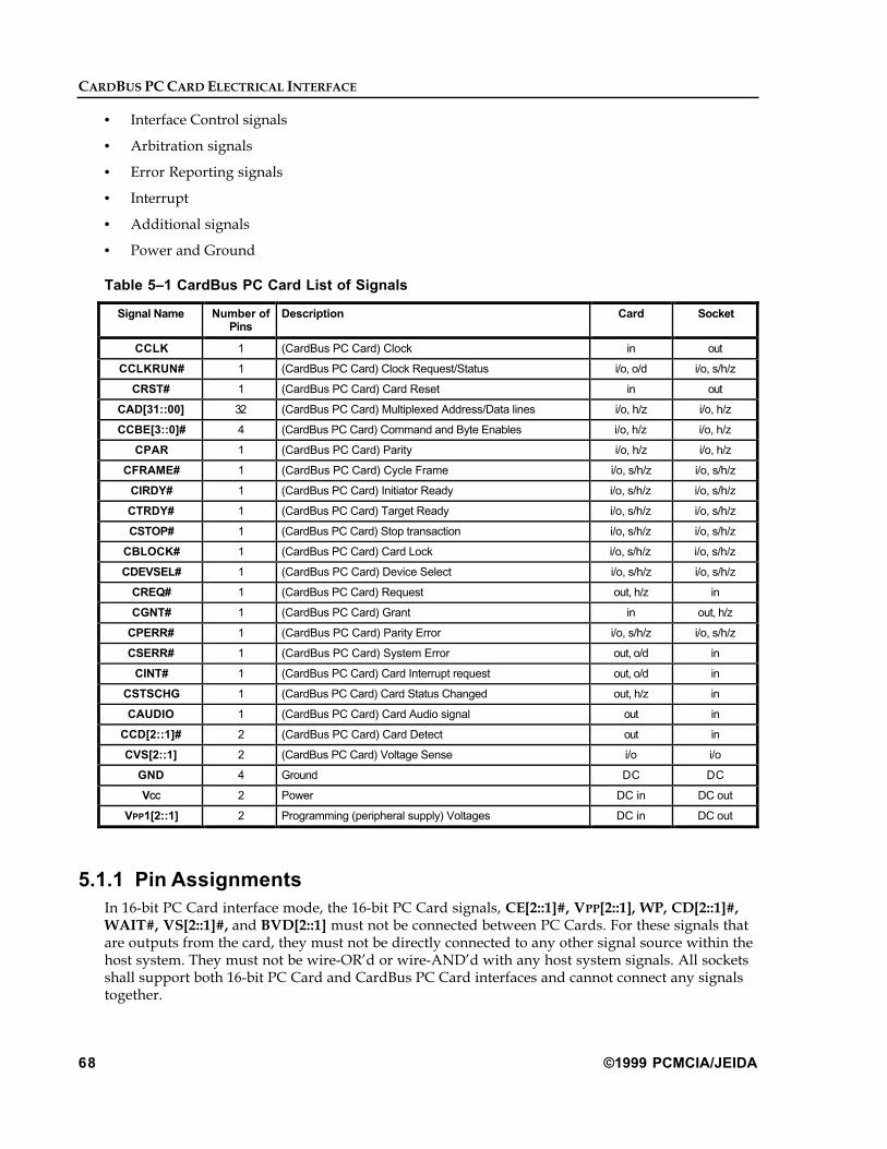
CARDBUS PC CARD ELECTRICAL INTERFACE
68 ©1999 PCMCIA/JEIDA
• Interface Control signals
• Arbitration signals
• Error Reporting signals
• Interrupt
• Additional signals
• Power and Ground
Table 5Ð1 CardBus PC Card List of Signals
Signal Name Number ofPins
Description Card Socket
CCLK 1 (CardBus PC Card) Clock in out
CCLKRUN# 1 (CardBus PC Card) Clock Request/Status i/o, o/d i/o, s/h/z
CRST# 1 (CardBus PC Card) Card Reset in out
CAD[31::00] 32 (CardBus PC Card) Multiplexed Address/Data lines i/o, h/z i/o, h/z
CCBE[3::0]# 4 (CardBus PC Card) Command and Byte Enables i/o, h/z i/o, h/z
CPAR 1 (CardBus PC Card) Parity i/o, h/z i/o, h/z
CFRAME# 1 (CardBus PC Card) Cycle Frame i/o, s/h/z i/o, s/h/z
CIRDY# 1 (CardBus PC Card) Initiator Ready i/o, s/h/z i/o, s/h/z
CTRDY# 1 (CardBus PC Card) Target Ready i/o, s/h/z i/o, s/h/z
CSTOP# 1 (CardBus PC Card) Stop transaction i/o, s/h/z i/o, s/h/z
CBLOCK# 1 (CardBus PC Card) Card Lock i/o, s/h/z i/o, s/h/z
CDEVSEL# 1 (CardBus PC Card) Device Select i/o, s/h/z i/o, s/h/z
CREQ# 1 (CardBus PC Card) Request out, h/z in
CGNT# 1 (CardBus PC Card) Grant in out, h/z
CPERR# 1 (CardBus PC Card) Parity Error i/o, s/h/z i/o, s/h/z
CSERR# 1 (CardBus PC Card) System Error out, o/d in
CINT# 1 (CardBus PC Card) Card Interrupt request out, o/d in
CSTSCHG 1 (CardBus PC Card) Card Status Changed out, h/z in
CAUDIO 1 (CardBus PC Card) Card Audio signal out in
CCD[2::1]# 2 (CardBus PC Card) Card Detect out in
CVS[2::1] 2 (CardBus PC Card) Voltage Sense i/o i/o
GND 4 Ground DC DC
VCC 2 Power DC in DC out
VPP1[2::1] 2 Programming (peripheral supply) Voltages DC in DC out
5.1.1 Pin AssignmentsIn 16-bit PC Card interface mode, the 16-bit PC Card signals, CE[2::1]#, VPP[2::1], WP, CD[2::1]#,WAIT#, VS[2::1]#, and BVD[2::1] must not be connected between PC Cards. For these signals thatare outputs from the card, they must not be directly connected to any other signal source within thehost system. They must not be wire-ORÕd or wire-ANDÕd with any host system signals. All socketsshall support both 16-bit PC Card and CardBus PC Card interfaces and cannot connect any signalstogether.

ELECTRICAL SPECIFICATION
© 1999 PCMCIA/JEIDA 69
The READY signal must not be connected between cards when the 16-bit PC Card interface socketsupports both I/O and Memory interfaces. It must not be wire-ORÕd or wire-ANDÕd with any hostsystem signals.
In systems which switch VCC individually to cards, no signal shall be directly connected betweencards other than ground.

CARDBUS PC CARD ELECTRICAL INTERFACE
70 ©1999 PCMCIA/JEIDA
Table 5Ð2 PC Card Pin 1 to Pin 34 Assignments
16-bit PC Card Interface CardBus PC Card Interface
Memory-Only I/O and Memory
Pin Signal I/O Notes Signal I/O Signal I/O Notes
1 GND DC GND DC GND DC
2 D3 I/O D3 I/O CAD0 I/O
3 D4 I/O D4 I/O CAD1 I/O
4 D5 I/O D5 I/O CAD3 I/O
5 D6 I/O D6 I/O CAD5 I/O
6 D7 I/O D7 I/O CAD7 I/O
7 CE1# I CE1# I CCBE0# I/O
8 A10 I A10 I CAD9 I/O
9 OE# I OE# I CAD11 I/O
10 A11 I A11 I CAD12 I/O
11 A9 I A9 I CAD14 I/O
12 A8 I A8 I CCBE1# I/O
13 A13 I A13 I CPAR I/O
14 A14 I A14 I CPERR# I/O
15 WE# I WE# I CGNT# I
16 READY O 1 IREQ# O CINT# O
17 VCC DC in VCC DC in VCC DC in
18 VPP1 DC in VPP1 DC in VPP1 DC in
19 A16 I A16 I CCLK I
20 A15 I A15 I CIRDY# I/O
21 A12 I A12 I CCBE2# I/O
22 A7 I A7 I CAD18 I/O
23 A6 I A6 I CAD20 I/O
24 A5 I A5 I CAD21 I/O
25 A4 I A4 I CAD22 I/O
26 A3 I A3 I CAD23 I/O
27 A2 I A2 I CAD24 I/O
28 A1 I A1 I CAD25 I/O
29 A0 I A0 I CAD26 I/O
30 D0 I/O D0 I/O CAD27 I/O
31 D1 I/O D1 I/O CAD29 I/O
32 D2 I/O D2 I/O RFU 2
33 WP O 1 IOIS16# O CCLKRUN# I/O
34 GND DC GND DC GND DC
"I" indicates signal is input to PC Card, "O" indicates signal is output from PC Card.1. Use of pin changes between the 16-bit PC Card Memory-Only and the I/O and Memory interface.2. Reserved for future use by the CardBus PC Card interface. CardBus PC Card sockets support both the
16-bit PC Card and CardBus PC Card interfaces therefore, the signals must be connected as definedfor the 16-bit PC Card interface when the CardBus PC Card adapter has detected a valid 16-bit PCCard insertion event.

ELECTRICAL SPECIFICATION
© 1999 PCMCIA/JEIDA 71
Table 5Ð3 PC Card Pin 35 to Pin 68 Assignments
16-bit PC Card Interface CardBus PC Card Interface
Pin Memory-Only I/O and Memory
Signal I/O Notes Signal I/O Signal I/O Notes
35 GND DC GND DC GND DC
36 CD1# O CD1# O CCD1# O
37 D11 I/O D11 I/O CAD2 I/O
38 D12 I/O D12 I/O CAD4 I/O
39 D13 I/O D13 I/O CAD6 I/O
40 D14 I/O D14 I/O RFU 2
41 D15 I/O D15 I/O CAD8 I/O
42 CE2# I CE2# I CAD10 I/O
43 VS1# O 4 VS1# O CVS1 I/O
44 RFU 1 IORD# I CAD13 I/O
45 RFU 1 IOWR# I CAD15 I/O
46 A17 I A17 I CAD16 I/O
47 A18 I A18 I RFU 2
48 A19 I A19 I CBLOCK# I/O
49 A20 I A20 I CSTOP# I/O
50 A21 I A21 I CDEVSEL# I/O
51 VCC DC in VCC DC in VCC DC in
52 VPP2 DC in VPP2 VPP2 DC in
53 A22 I A22 I CTRDY# I/O
54 A23 I A23 I CFRAME# I/O
55 A24 I A24 I CAD17 I/O
56 A25 I A25 I CAD19 I/O
57 VS2# 5 VS2# CVS2 I/O
58 RESET I 3 RESET I CRST# I
59 WAIT# O 3 WAIT# O CSERR# O
60 RFU 1 INPACK# O CREQ# O
61 REG# I 1 REG# I CCBE3# I/O
62 BVD2 O 1 SPKR# O CAUDIO O
63 BVD1 O 1 STSCHG# O CSTSCHG O
64 D8 I/O D8 I/O CAD28 I/O
65 D9 I/O D9 I/O CAD30 I/O
66 D10 I/O D10 I/O CAD31 I/O
67 CD2# O CD2# O CCD2# O
68 GND DC GND DC GND DC
3. RESET and WAIT# are RFU in PCMCIA 1.0 / JEIDA 4.0 version of the Standard. These signals arerequired in PCMCIA 2.0 / JEIDA 4.1 and all later versions of the Standard.
4. VS1# was named RFSH in PCMCIA 2.1 / JEIDA 4.2 and earlier versions of the Standard.5. VS2# was RFU in PCMCIA 2.1 / JEIDA 4.2 and earlier versions of the Standard.

CARDBUS PC CARD ELECTRICAL INTERFACE
72 ©1999 PCMCIA/JEIDA
5.1.2 Signal/Pin Description
5.1.2.1 System Pins
CCLK input tocard
CardBus PC Card Clock provides timing for all transactions on the CardBus PC Card interface and isan input to every CardBus PC Card device. All other CardBus PC Card signals, except CRST# (uponassertion), CCLKRUN#, CINT#, CSTSCHG, CAUDIO, CCD[2::1]#, and CVS[2::1], are sampled onthe rising edge of CCLK, and all timing parameters are defined with respect to this edge. CardBus PCCard operates up to 33ÊMHz. Also, the clock can be stopped in the low state. (See 5.3.2.2.1 ClockSpecifications and see also 5.2.10 Clock Control.)
CCLKRUN# i/o, o/dfor card
CardBus PC Card Clock Run is a signal which is used by cards to request starting (or speeding up)the CardBus PC Card clock, CCLK. CCLKRUN# also indicates the clock status. For PC Cards,CCLKRUN# is an open drain output and also an input. For the host system, it is a Sustained High-Zstate I/O signal. A CardBus PC Card requests the host system to start, speed up or maintain theinterface clock by assertion of CCLKRUN#. The host system is responsible for maintainingCCLKRUN# asserted, and for driving it high to the negated state.
CRST# input tocard
CardBus PC Card Reset is used to bring CardBus PC Card specific registers, sequencers, andsignals to a consistent state. What effect CRST# has on an agent beyond the CardBus PC Cardsequencer is beyond the scope of this specification, except for the reset states of required CardBus PCCard configuration registers. Anytime CRST# is asserted, all CardBus PC Card output signals mustbe driven to their benign state. In general, this means they must be in a High-Z state. CSERR#, CINT#,and CCLKRUN# (open drain) are floated. CREQ# must be in a High-Z state (it cannot be driven lowor high during reset). CGNT# must be negated. To prevent CAD[31::00], CCBE[3::0]#, and CPARsignals from floating during reset, the central resource may drive these lines during reset but only to alow voltage level, they may not be driven high. CVS[2::1] must be driven low. The states ofCCD[2::1]#, and CSTSCHG are not affected by CRST#. The CSTSCHG signal may actually pulsewhile CRST# is asserted.
CRST# may be asynchronous to CCLK when asserted. Negation of CRST# is synchronous to CCLK
5.1.2.2 Address and Data Pins
CAD[31::00] i/o, h/z CardBus PC Card Address and Data are multiplexed on the same CardBus PC Card pins. A bustransaction consists of an address phase followed by one or more data phases. CardBus PC Cardsupports both read and write bursts.
The address phase is the clock cycle in which CFRAME# is asserted. During the address phase,CAD[31::00] contain a physical address (32 bits). For I/O, this is a byte address; for configuration andmemory it is a DWORD address. During data phases, CAD[07::00] contain the least significant byte(LSB) and CAD[31::24] contain the most significant byte (MSB)4. Write data is stable and valid whenCIRDY# is asserted and read data is stable and valid when CTRDY# is asserted. Data is transferredduring those clocks where both CIRDY# and CTRDY# are asserted.
CCBE[3::0]# i/o, h/z CardBus PC Card Command and Byte Enables are multiplexed on the same CardBus PC Card pins.During the address phase of a transaction, CCBE[3::0]# define the bus command (refer to the BusCommands section of this specification for bus command definitions). During the data phase,CCBE[3::0]# are used as Byte Enables. The Byte Enables are valid for the entire data phase anddetermine which byte lanes carry meaningful data. CCBE[0]# applies to byte 0 (LSB) and CCBE[3]#applies to byte 3 (MSB).
CPAR i/o, h/z CardBus PC Card Parity is even5 parity across CAD[31::00] and CCBE[3::0]#. Parity generation isrequired by all CardBus PC Card agents. CPAR is stable and valid one clock after the address phase.For data phases CPAR is stable and valid one clock after either CIRDY# is asserted on a writetransaction or CTRDY# is asserted on a read transaction. Once CPAR is valid, it remains valid untilone clock after the completion of the current data phase. (CPAR has the same timing as CAD[31::00]but delayed by one clock.) The master drives CPAR for address and write data phases; the targetdrives CPAR for read data phases.
4Bit order follows the convention where: bit 0 is LSB and bit 31 is MSB.5 The number of "1"s on CAD[31::00] , CCBE[3::0]# , and CPAR equal an even number.

ELECTRICAL SPECIFICATION
© 1999 PCMCIA/JEIDA 73
5.1.2.3 Interface Control Pins
CFRAME# i/o, s/h/z CardBus PC Card Cycle Frame is driven by the current master to indicate the beginning and durationof a transaction. CFRAME# is asserted to indicate that a bus transaction is beginning. WhileCFRAME# is asserted, data transfers continue. When CFRAME# is negated, the transaction is in thefinal data phase.
CIRDY# i/o, s/h/z CardBus PC Card Initiator Ready indicates the initiating agent's (bus master's) ability to complete thecurrent data phase of the transaction. CIRDY# is used in conjunction with CTRDY#. A data phase iscompleted on any clock both CIRDY# and CTRDY# are sampled asserted. During a write, CIRDY#indicates that valid data is present on CAD[31::00]. During a read, it indicates the master is preparedto accept data. Wait cycles are inserted until both CIRDY# and CTRDY# are asserted together.
CTRDY# i/o, s/h/z CardBus PC Card Target Ready indicates the agent's (selected target's) ability to complete the currentdata phase of the transaction. CTRDY# is used in conjunction with CIRDY#. A data phase is completedon any clock both CTRDY# and CIRDY# are sampled asserted. During a read, CTRDY# indicates thatvalid data is present on CAD[31::00]. During a write, it indicates the target is prepared to accept data.Wait cycles are inserted until both CIRDY# and CTRDY# are asserted together.
CSTOP# i/o, s/h/z CardBus PC Card Stop indicates the current target is requesting the master to stop the currenttransaction.
CBLOCK# i/o, s/h/z CardBus PC Card Lock is an optional signal which indicates an atomic operation that may requiremultiple transactions to complete. When CBLOCK# is asserted, non-exclusive transactions mayproceed to an address that is not currently locked. A grant to start a transaction on CardBus PC Carddoes not guarantee control of CBLOCK#. Control of CBLOCK# is obtained under its own protocol inconjunction with CGNT#. It is possible for different agents to use CardBus PC Card while a singlemaster retains ownership of CBLOCK#. If a CardBus PC Card implements shared memory, it mustalso implement CBLOCK# and guarantee complete access exclusion in that memory. Host bridgesthat have system memory behind them must also implement CBLOCK#.
CDEVSEL# i/o, s/h/z CardBus PC Card Device Select, when actively driven, indicates the driving device has decoded itsaddress as the target of the current access. As an input, CDEVSEL# indicates whether any device onthe bus has been selected.
5.1.2.4 Arbitration Pins (Bus Masters Only)
CREQ# out, h/zfor card
CardBus PC Card Request indicates to the arbiter that this agent desires use of the bus. Every masterhas its own CREQ#.
CGNT# out, h/zforsocket
CardBus PC Card Grant indicates to the agent that access to the bus has been granted. Every masterhas its own CGNT#.

CARDBUS PC CARD ELECTRICAL INTERFACE
74 ©1999 PCMCIA/JEIDA
5.1.2.5 Error Reporting Pins
The error reporting pins are required by all devices.
CPERR# i/o, s/h/z CardBus PC Card Parity Error is only for the reporting of data parity errors during all CardBus PCCard transactions except a Special Cycle. The CPERR# pin is sustained tri-state and must be drivenactive by the agent receiving data two clocks following the data when a data parity error is detected.The minimum duration of CPERR# is one clock for each data phase that a data parity error is detected.If sequential data phases each have a data parity error, the CPERR# signal will be asserted for morethan a single clock. CPERR# must be driven high for one clock before being tri-stated as with allsustained tri-state signals. There are no special conditions when a data parity error may be lost orwhen reporting of an error may be delayed. An agent cannot report a CPERR# until it has claimed theaccess by asserting CDEVSEL# and completed a data phase.
CSERR# out, o/dfor card
CardBus PC Card System Error is for reporting address parity errors, data parity errors on the SpecialCycle command, or any other system error where the result could be catastrophic. If an agent does notwant a non-maskable interrupt (NMI) to be generated, a different reporting mechanism is required.CSERR# is pure open drain and is actively driven for a single CardBus PC Card clock by the agentreporting the error. The assertion of CSERR# is synchronous to the clock and meets the setup and holdtimes of all bused signals. However, the restoring of CSERR# to the negated state is accomplished bya weak pull-up (same value as used for s/h/z) which is provided by the system designer and not by thesignaling agent or central resource. This pull-up may take two to three clock periods to fully restoreCSERR#. The agent that reports CSERR#s to the operating system does so anytime CSERR# issampled asserted.
5.1.2.6 Interrupt Request Pin
CINT# out, o/dfor card
Card Interrupt Request is an optional signal which is defined as level sensitive, and asserted low(negative true), using an open drain output driver. The assertion and negation of CINT# isasynchronous to CCLK. Single function and multi-function6 cards are supported. The system vendor isfree to combine the various CINT# signals from CardBus PC Card connectors in any way to connectthem to the interrupt controller. This means the device driver may not make any assumptions aboutinterrupt sharing. All CardBus PC Card device drivers must be able to share an interrupt (chaining)with any other logical device, including functions on the same multi-function card.
CINT# is asserted while the INTR field of the Function Event Mask Register is set (1) and either orboth the INTR field of the Function Event Register is set (1) or the INTR field of the Function PresentState Register is set (1). (See 5.2.11.3 Register Descriptions)
5.1.2.7 Additional Signals
CSTSCHG out, h/zfor card
Card Status Changed is an optional signal used to alert the system to changes in the READY, WP, orBVD[2::1] conditions of the card. It is also used for the system and/or CardBus PC Card interfaceWake up. CSTSCHG is asynchronous to CCLK.
CSTSCHG is asserted while any field in the Function Event Mask Register other than INTR is set (1)and the field of the same name in the Function Event Register is set (1). (See 5.2.11.3 RegisterDescriptions)
CAUDIO outfor card
Card Audio is an optional digital audio output signal from a PC Card to the system's speaker. CardBusPC Card supports two types of audio signals: a single amplitude, binary waveform, and/or Pulse WidthModulation (PWM) encoded signal. CAUDIO has no relationship to CCLK
CCD[2::1]#,CVS[2::1]#,VCC,VPP[2::1]GND
(See 2. Common Pin Description.)
6 When several independent functions are integrated into a single PC Card, it is referred to as a multi-function card.
Each function on a multi-function card has its own configuration space.

ELECTRICAL SPECIFICATION
© 1999 PCMCIA/JEIDA 75
5.1.3 Central Resource FunctionsThroughout this specification the term central resource is used to describe CardBus PC Card supportfunctions supplied by the host system, typically in the host CardBus PC Card adapter or in aCardBus PC Card compliant bridge. These functions may include, but are not limited to, thefollowing:
• Central Arbitration,
• Required signal pull-ups or "keepers" (See 5.3.3.3 Pull-ups.),
• Default ownership of the interface, and
• CardBus PC Card Clock control.
5.2 CardBus PC Card OperationThe CardBus PC Card specification requires strong ordering of all transactions and operands acrossthe interface.
5.2.1 Bus CommandsBus Commands indicate to the target the type of transaction the master is requesting. BusCommands are encoded on the CCBE[3::0]# lines during the address phase.
5.2.1.1 Command Definition
CardBus PC Card Bus Command encodings and types are as listed below, followed by a briefdescription of each. Note that the command encodings are as viewed on the bus where a "1"indicates a high voltage and "0" is a low voltage. Byte Enables are asserted when 0.
Table 5Ð4 CardBus PC Card Commands
CCBE[3::0]# Command type
0000000100100011010001010110011110001001101010111100110111101111
AllocatedSpecial CycleI/O ReadI/O WriteReservedReservedMemory ReadMemory WriteReservedReservedConfiguration ReadConfiguration WriteMemory Read MultipleAllocatedMemory Read LineMemory Write and Invalidate
Allocated indicates that the command encoding is not defined for CardBus PC Card, and must not bedefined as other environments use the encoding. The purpose of allocated command encodings is tomaintain compatibility between CardBus PC Card and other environments. CardBus PC Cardtargets must not alias allocated commands with other commands. Targets must not respond toallocated encodings. If an allocated encoding is used on the interface, the access typically will beterminated with master-abort.
CARDBUS PC CARD ELECTRICAL INTERFACE
76 ©1999 PCMCIA/JEIDA
The Special Cycle command provides a simple message broadcast mechanism on CardBus PC Card.It is designed to be used as an alternative to physical signals when sideband communication isnecessary. (See 5.2.7.2 Special Cycle.)
The I/O Read command is used to read data from an agent mapped in I/O address space.CAD[31::00] provide a byte address. All 32 bits must be decoded. The Byte Enables indicate thesize of the transfer and must be consistent with the byte address.
The I/O Write command is used to write data to an agent mapped in I/O address space. All 32 bitsmust be decoded. The Byte Enables indicate the size of the transfer and must be consistent with thebyte address.
Reserved command encodings are reserved for future use. CardBus PC Card targets must not aliasreserved commands with other commands. Targets must not respond to reserved encodings. If areserved encoding is used on the interface, the access typically will be terminated with master-abort.
The Memory Read command is used to read data from an agent mapped in the memory addressspace. The target is free to do an anticipatory read for this command only if it can guarantee thatsuch a read will have no side effects. Furthermore, the target must ensure the coherency (whichincludes ordering) of any data retained in temporary buffers after this CardBus PC Card transactionis completed. Such buffers must be invalidated before any synchronization events (e.g., updatingan I/O Status register or memory flag) are passed through this access path.
The Memory Write command is used to write data to an agent mapped in the memory address space.When the target returns "ready," it has assumed responsibility for the coherency (which includesordering) of the subject data. This can be done either by implementing this command in a fullysynchronous manner, or by insuring any software transparent posting buffer will be flushed beforesynchronization events (e.g., updating an I/O Status register or memory flag) are passed throughthis access path. This implies that the master is free to create a synchronization event immediatelyafter using this command.
The Configuration Read command is used to read the configuration space of each agent. An agent isselected when its CFRAME# signal is asserted and CAD[1::0] are 00. During the address phase of aconfiguration cycle, CAD[7::2] address one of the 64 DWORD registers (where byte enables addressthe byte(s) within each DWORD) in the configuration space of each device and CAD[31::11] arelogical don't cares. CAD[10::08] indicate which device of a multi-function agent is being addressed.
The Configuration Write command is used to transfer data to the configuration space of each agent.An agent is selected when the CFRAME# signal is asserted and CAD[1::0] are 00. During theaddress phase of a configuration cycle, the CAD[7::2] lines address the 64 DWORD (where byteenables address the byte(s) within each DWORD) configuration space of each device andCAD[31::11] are logical don't cares. CAD[10::08] indicate which device of a multi-function agent isbeing addressed.
The Memory Read Multiple command is semantically identical to the Memory Read command exceptthat it additionally indicates that the master may intend to fetch more than one cache line beforedisconnecting. The memory controller should continue pipelining memory requests as long asCFRAME# is asserted. This command is intended to be used with bulk sequential data transferswhere the memory system (and the requesting master) might gain some performance advantage bysequentially reading ahead an additional cache line when a software transparent buffer is availablefor temporary storage.
The Memory Read Line command is semantically identical to the Memory Read command except thatit additionally indicates that the master intends to complete more than two 32-bit CardBus PC Carddata phases. This command is intended to be used with bulk sequential data transfers where thememory system (and the requesting master) might gain some performance advantage by reading

ELECTRICAL SPECIFICATION
© 1999 PCMCIA/JEIDA 77
up to a cache line boundary in response to the request rather than a single memory cycle. As withthe Memory Read command, pre-fetched buffers must be invalidated before any synchronizationevents are passed through this access path.
The Memory Write and Invalidate command is semantically identical to the Memory Write commandexcept that it additionally guarantees a minimum transfer of one complete cache line; i.e., themaster intends to write all bytes within the addressed cache line in a single CardBus PC Cardtransaction. The master may allow the transaction to cross a cache line boundary only if it alsointends to transfer the entire next line. This command requires implementation of a configurationregister in the master indicating the cache line size. A target containing memory which might becacheable by the host system is also required to implement the Cache Line Size register. (See 5.2.9Cache Support and 5.4.2.1 Configuration Space.) The target containing cacheable memory mustaccept a full cache line before disconnecting the transaction if it completes the first data phase. Thiscommand allows a memory performance optimization by invalidating a dirty line in a write-backcache without requiring the actual write-back cycle, thus shortening access time. (See also 5.2.3.3.1Master Initiated Termination.)
5.2.1.2 Command Usage Rules
All CardBus PC Card agents are required to respond as a target to configuration (read and write)commands. All other commands are optional. Command execution order on the CardBus PC Card isguaranteed for I/O (read and write) commands. CardBus PC Card targets that contain relocatablefunctions or registers are required to allow them to be mapped to memory space through theconfiguration registers. This is to provide for the option of using the device in configurations whereI/O space is not available. When such mapping is done, command execution order will beguaranteed by the system designer whether the device is used in I/O or memory space. Memoryreads and writes to a mapped device constitute "memory mapped I/O."
A master may implement the optional commands as needed. A target may also implement theoptional commands as needed, but if it implements basic memory commands, it must support allthe memory commands, including Memory Write and Invalidate, Memory Read Line, and MemoryRead Multiple. This means that, if the target intends to complete the first data phase, it musttranslate the requested command to a memory command it has implemented. For example, a targetmight not implement the Memory Read Line command; however, it must accept the request (if theaddress is decoded for a memory access) and treat it as a Memory Read command. Similarly, a non-cacheable target might not implement the Memory Write and Invalidate command, but must acceptthe request (if the address is decoded for a memory access) and treat it as a Memory Writecommand.
For block data transfer to/from system memory, Memory Write and Invalidate and Read MemoryLine are the recommended commands for masters capable of supporting them. The Memory Reador Memory Write commands can be used if for some reason the master is not capable of using theperformance optimizing commands.
For masters using Memory Read commands, any length access will work for all commands,however the preferred use is shown below. While Write and Invalidate is the only command thatrequires implementation of the Cache Line Size register, it is strongly suggested the Memory Readcommands use it as well. In all cases, the bridge is responsible for the correctness of any latent data.Preferred use is shown for both cases (with and without using the Cache Line Size register).
The preferred use when using the Cache Line Size register is:
Memory Read command use when bursting one half or less of a cache line
Memory Read Line command use when bursting more than one half of a cache line to three cache lines
Memory Read Multiple command use when bursting more than three cache lines

CARDBUS PC CARD ELECTRICAL INTERFACE
78 ©1999 PCMCIA/JEIDA
The preferred use when not using the Cache Line Size register is:
Memory Read command use when bursting two or less data transfers
Memory Read Line command use when bursting 3 to 12 data transfers
Memory Read Multiple command use when doing long bursts (13 or more data transfers)
5.2.2 CardBus PC Card Protocol FundamentalsThe basic bus transfer mechanism on CardBus PC Card is a burst. A burst is composed of anaddress phase and one or more data phases. CardBus PC Card supports bursts in both memory andI/O address spaces. The host bridge (that resides between the host processor and CardBus PC Card)may merge (or assemble) memory write accesses into a single transaction when no side effects exist.A device indicates no side effects (allow prefetching of read data and merging of write data in anyorder) by setting the prefetch bit in the Base Address register (refer to the Base Address Registersection of this specification). A bridge may distinguish where merging is allowed and where it isnot by an address range which could be provided by configuration software during initialization.Merging of data into that buffer must stop (and the buffer flushed) when a subsequent write occursthat is not prefetchable or a read occurs to any range. Write transactions following either of thesetwo events may be merged with subsequent writes, but not to previously merged data, even if inthe prefetchable range.
The host bridge may always combine sequential DWORDs (memory write) generated by theprocessor into bursts as long as the implied address ordering (associated with each DWORD) is thesame. For example, the bridge may create a burst when the processor write sequence is DWORD 0,DWORD 2, and DWORD 3. The CardBus PC Card burst sequence could be DWORD 0, DWORD 1(no byte enables), DWORD 2 and complete the burst with DWORD 3. Combining is allowedanytime the next DWORD address is more significant than the previous one. The bridge mayconvert single Processor (memory) read requests into a read burst (reading ahead of the processor)when the read will not cause a side effect in the addressed target.
Since I/O accesses from the processor cannot be combined, they will normally only have a singledata phase. Currently, no known processor or bus master generates bursts in I/O space. However,if in the future some new device is capable of generating meaningful I/O bursts (e.g., accessing aFIFO port), it will not be precluded. There is no implied addressing on I/O bursts. When I/Obursts are done, the target and master must understand the implied addressing. CardBus PC Carddevices that do not deal with multiple I/O data phases must disconnect the access after the first dataphase. To ensure that I/O devices will operate correctly, bridges may never merge or combinesequential I/O accesses into a single CardBus PC Card access or burst. All I/O accesses must appearon CardBus PC Card exactly as the processor generated them. (If a target of an I/O access is selectedby its address but the byte enables indicate a transfer larger than the device supports, the targetterminates with target-abort.)
All signals are sampled on the rising edge of the clock7. Each signal has a setup and hold aperturewith respect to the rising clock edge, in which transitions are not allowed. Outside this aperture,signal values or transitions have no significance. This aperture occurs only on qualified rising clockedges for CAD[31::00] and CPAR8 signals,9 and on every rising clock edge for CBLOCK#,CIRDY#, CTRDY#, CFRAME#, CDEVSEL#, CSTOP#, CREQ#, CGNT#, CSERR# (only onassertion), CRST# (only on negation), and CPERR#. CCBE[3::0]#, as bus commands, are qualifiedon the clock edge that CFRAME# is first asserted. CCBE[3::0]#, as byte enables, are qualified on
7 The exceptions are CINT#, CSTSCHG#, CCLKRUN# , CAUDIO , CCD[2::1]# , and CVS[2::1] which are
discussed inthe Signal Definition Section.8 CPAR is treated like a CAD line delayed by one clock.9 The notion of qualifying CAD signals is fully defined in 5.2.7.3 Address/Data Stepping.

ELECTRICAL SPECIFICATION
© 1999 PCMCIA/JEIDA 79
each rising clock edge following the completion of an address phase or data phase. CINT#,CSTSCHG, CCLKRUN#, CAUDIO, CCD[2::1]#, and CVS[2::1] are not qualified or synchronous.
5.2.2.1 Basic Transfer Control
The fundamentals of all CardBus PC Card data transfers are controlled with three signals. (SeeFigure 5-1 CardBus PC Card Basic Read Operation.)
CFRAME# is driven by the master to indicate the beginning and end of a transaction.
CIRDY# is driven by the master, allowing it to force wait cycles.
CTRDY# is driven by the target, allowing it to force wait cycles.
The interface is IDLE when both CFRAME# and CIRDY# are negated. The first clock edge onwhich CFRAME# is asserted is the address phase, and the address and bus command code aretransferred on that clock edge. The next clock edge begins the first of one or more data phases,during which data is transferred between master and target on each clock edge for which bothCIRDY# and CTRDY# are asserted. Wait cycles may be inserted in a data phase by either themaster or the target with CIRDY# and CTRDY# signals respectively.
The source of the data is required to assert its CXRDY# signal unconditionally when data is valid(CIRDY# on a write transaction, CTRDY# on a read transaction). The receiving agent may assert itsCXRDY# as it chooses.
Once a master has asserted CIRDY# it cannot change CIRDY# or CFRAME# until the current dataphase completes regardless of the state of CTRDY#. Once a target has asserted CTRDY# orCSTOP# it cannot change CDEVSEL#, CTRDY#, or CSTOP# until the current data phasecompletes. Neither the master nor the target can change its mind once it has committed to the datatransfer.
At such time as the master intends to complete only one more data transfer (which could beimmediately after the address phase), CFRAME# is negated and CIRDY# is asserted indicating themaster is ready. After the target indicates the final data transfer (CTRDY# is asserted), the interfacereturns to the IDLE state with both CFRAME# and CIRDY# negated.
5.2.2.2 Addressing
CardBus PC Card defines three physical address spaces. The memory and I/O address spaces arecustomary. The configuration address space has been defined to support CardBus PC Cardhardware configuration. (See also 5.2.7.4.1 Generating Configuration Cycles.)
CardBus PC Card targets that contain relocatable functions or registers are required to allow them tobe mapped to memory space through the Base Address registers located in the CardBus PC Cardconfiguration space. This is to provide for the option of using the device in system configurationswhere I/O space is not available.
Address decoding on CardBus PC Card is distributed, i.e., done on every device. This obviates theneed for central decode logic, or for device select signals. Each agent is responsible for its ownaddress decode. CardBus PC Card supports two styles of address decoding, positive and subtractive.Positive decoding is faster since each device is looking for accesses in the address range(s) that it hasbeen assigned. Subtractive decoding can be implemented by only one device on the bus, since itaccepts all accesses not positively decoded by some other agent. This decode mechanism is slowersince it must give all other bus agents a "first right of refusal" on the access. However, it is veryuseful for an agent that must respond to a highly fragmented address space. Targets that performeither positive or negative decode must not respond (assert CDEVSEL#) to reserved or allocated buscommands.

CARDBUS PC CARD ELECTRICAL INTERFACE
80 ©1999 PCMCIA/JEIDA
The information contained in the two low order address bits (CAD[1::0]) varies by address space. Inthe I/O address space, all 32 CAD lines are used to provide a full byte address. This allows anagent requiring byte level address resolution to complete address decode and claim the cycle10
without waiting an extra cycle for the byte enables (thus delaying all subtractive decode cycles byan extra clock). CAD[1::0] are used for the generation of CDEVSEL# only and indicate the leastsignificant valid byte involved in the transfer. For example, if CCBE0# were asserted thenCAD[1::0] would be 00; if only CCBE3# were asserted, then CAD[1::0] would be 11. Once a targethas claimed an I/O access (using CAD[1::0]), it then determines if it can complete the entire accessas indicated in the byte enables. If all the selected bytes are not in the selected target's addressrange, the entire access cannot be completed. In this case, the target does not transfer any data, butterminates with a target-abort.
The table below summarizes the encoding of CAD[1::0].
Table 5Ð5 Address Bus Encoding
CAD1 CAD0 CCBE3# CCBE2# CCBE1# CCBE0#
0 0 X X X 0
0 1 X X 0 1
1 0 X 0 1 1
1 1 0 1 1 1
The above table is for decode purposes only and only applies to a device that does not control allbytes within a single I/O DWORD. Such devices must terminate the cycle with target abort for anybyte enable/CAD[1::0] combination not in the above table. However, devices that "own" all bytesin the I/O DWORD do not have to check for illegal byte enable/CAD[1::0] combinations. Instead,they may ignore CAD1 and CAD0 (i.e., claim the cycle based on the DWORD address and performthe operation described by the byte enables). Note that any combination of byte enables is valid,including none. (A device may restrict which combination of byte enables its device driver mayuse.)
All targets are required to check CAD[1::0] during a memory command transaction, and eitherprovide the requested burst order, or execute a target disconnect with or after the first data phase.Implementation of linear burst ordering is required by all devices that can support bursting.Implementing other burst order modes is not required. In the memory address space, accesses aredecoded to a DWORD address using CAD[31::02]. In linear incrementing mode, the address isassumed to increment by one DWORD after each data phase until the transaction is terminated.
During Memory commands, CAD[1::0] have the following meaning:
CAD1 CAD0 Burst Order
0 0 Linear address incrementing
0 1 Reserved (disconnect after first data phase)
1 X Reserved (disconnect after first data phase)
In the configuration address spaces, accesses are decoded to a DWORD address using CAD[7::2]. Anagent determines that it is the target of the access (asserts CDEVSEL#) when a configurationcommand is decoded and CAD[1::0] are 00. Otherwise, the agent ignores the current transaction. Abridge determines that a configuration access is for a device behind it by decoding a configuration
10 Standard PC address assignments in the I/O space are such that separate physical devices may share the same
DWORD address. This means that in certain cases a full byte address is required for the device to claim the access(assert CDEVSEL# ).

ELECTRICAL SPECIFICATION
© 1999 PCMCIA/JEIDA 81
command, its bridge number, and that CAD[1::0] are 01. For more details about configurationaccesses refer to the (See also 5.2.7.4.1 Generating Configuration Cycles.)
5.2.2.3 Byte Alignment
Byte lane swapping is not done on CardBus PC Card since all CardBus PC Card compliant devicesmust connect to all 32 address/data bits for address decode purposes. This means that bytes willalways appear in their natural byte lane, based upon byte address.
Furthermore, CardBus PC Card does not support automatic bus sizing. In general, software is awareof the characteristics of the target device and only issues appropriate length accesses.
The byte enables alone are used to determine which bytes carry meaningful data. The byte enablesare free to change between data phases but must be valid on the edge of the clock that starts eachdata phase and must stay valid for the entire data phase. (See Figure 5-1 CardBus PC Card BasicRead Operation) and note that data phases begin on clocks 3, 5, and 7. Changing byte enablesduring a read burst transaction is generally not useful, but is permitted.) The master is free tochange the byte enables on each new data phase (although the read diagram does not show this). Ifthe master changes byte enables on a read transaction, it does so with the same timing as would beused in a write transaction. If byte enables are important for the target on a read transaction, thetarget must wait for the byte enables to be valid on each data phase before completing the transfer;otherwise, it must return all bytes.
Targets are only required to return the bytes indicated by the byte enables. However, if a targetsupports prefetching of data (see the Socket Service Specification) it must return all bytes regardlessof which byte enables are asserted. Prefetching should not be enabled if there are side effects, e.g.data loss or a status change because of the access. A target should not return bytes not indicated bythe byte enables if reading those bytes has any side effects.
CardBus PC Card allows any contiguous or non-contiguous combination of byte enables. If no byteenables are asserted, the target of the access must complete the transaction by asserting CTRDY#and providing parity if a read request. The target of an access where no byte enables are assertedmust complete the current data phase without any permanent change. On a read transaction, thismeans that data or status are not changed. If completing the access has no affect on the data orstatus, then the target may complete the access by either providing data or not. The target (on aread) must provide parity across CAD[31::0] and CCBE[3::0]# regardless of the state of the byteenables. On a write transaction, the data is not stored but CPAR is valid.
However, some targets may not be able to properly interpret non-contiguous patterns (e.g. bridgesthat interface to 8- and 16-bit slaves). If this occurs, a target (bus bridge) may optionally report anillegal pattern as an asynchronous error (CSERR#) or, if capable, break the transaction into two 16-bit transactions that are legal for the intended agent. On an I/O access, the target is required tosignal target-abort if unable to complete the entire access defined by the byte enables.
5.2.2.4 Bus Driving and Turnaround
A turnaround cycle is required on all signals that may be driven by more than one agent. Theturnaround cycle is required to avoid contention when one agent stops driving a signal and anotheragent begins. This is indicated on the timing diagrams as two arrows pointing at each others' tail.This turnaround cycle occurs at different times for different signals. For instance, CIRDY#,CTRDY#, CDEVSEL#, and CSTOP# use the address phase as their turnaround cycle. CFRAME#,CCBE[3::0]#, and CAD[31::00] use the IDLE cycle between transactions as their turnaround cycle.The turnaround cycle for CBLOCK# occurs one clock after the current owner releases it. CPERR#has a turnaround cycle on the fourth clock after the last data phase, which is three clocks after the

CARDBUS PC CARD ELECTRICAL INTERFACE
82 ©1999 PCMCIA/JEIDA
turnaround cycle for the CAD lines. An IDLE cycle is when both CFRAME# and CIRDY# arenegated (e.g., clock 9 in Figure 5-1).
All CAD lines must be driven to stable values during every address and data phase. Even bytelanes not involved in the current data transfer must physically drive stable (albeit meaningless)data onto the bus. The motivation is for parity calculations and to keep input buffers on byte lanesnot involved in the transfer from switching at the threshold level and more generally to facilitatefast, metastability free latching. In power sensitive applications, it is recommended that, in theinterest of minimizing bus switching power consumption, byte lanes not being used in the currentbus phase should be driven with the same data as contained in the previous bus phase. Inapplications that are not power sensitive, the agent driving the CAD lines may drive whatever itdesires on unused byte lanes. Parity must be calculated on all bytes regardless of the byte enables.
5.2.3 Bus TransactionsTiming diagrams show the relationship of significant signals involved in 32-bit transactions. When asignal is drawn as a solid line, it is actively being driven by the current master or target. When asignal is drawn as a dashed line, no agent is actively driving it. However, it may still be assumedto contain a stable value if the dashed line is at the high rail. High-Z signals are indicated to haveindeterminate values when the dashed line is between the two rails (e.g., CAD or CCBE# lines).When a solid line becomes a dotted line, it indicates the signal was actively driven and now isHigh-Z. When a solid line makes a low to high transition and then becomes a dotted line, itindicates the signal was actively driven high to precharge the bus, and then switched to the High-Zstate. The cycles before and after each transaction will be discussed in the arbitration section.
5.2.3.1 Read Transaction
Figure 5-1 illustrates a read transaction and starts with an address phase which occurs whenCFRAME# is asserted for the first time and occurs on clock 2. During the address phaseCAD[31::00] contain a valid address and CCBE[3::0]# contain a valid bus command.

ELECTRICAL SPECIFICATION
© 1999 PCMCIA/JEIDA 83
CFRAME#
CCLK
CTRDY#
CIRDY#
CAD
CDEVSEL#
CCBE# BE#'s
ADDRESSPHASE
DATAPHASE
DATAPHASE
DATAPHASE
BUS CMD
DATA-1 DATA-2 DATA-3ADDRESS
DA
TA
TR
AN
SF
ER
DA
TA
TR
AN
SF
ER
DA
TA
TR
AN
SF
ER
WA
IT
WA
IT
WA
IT
BUS TRANSACTION
1 2 3 4 5 6 7 8 9
Figure 5-1 CardBus PC Card Basic Read Operation
The first clock of the first data phase is clock 3. During the data phase CCBE# indicate which bytelanes are involved in the current data phase. A data phase may consist of a data transfer and waitcycles. The CCBE# output buffers must remain enabled (for both read and writes) from the firstclock of the data phase through the end of the transaction. This ensures CCBE# are not left floatingfor long intervals.
The first data phase on a read transaction requires a turnaround-cycle (enforced by the target viaCTRDY#). In this case the address is valid on clock 2 and then the master stops driving CAD. Theearliest the target can provide valid data is clock 4. The target must drive the CAD lines followingthe turnaround cycle when CDEVSEL# is asserted. Once enabled, the output buffers must stayenabled through the end of the transaction. (This ensures CAD are not left floating for longintervals.)
A data phase completes when data is transferred, which occurs when both CIRDY# and CTRDY#are asserted on the same clock edge. (CTRDY# cannot be driven until CDEVSEL# is asserted.)When either is negated a wait cycle is inserted and no data is transferred. As noted in the diagram,data is successfully transferred on clocks 4, 6, and 8, and wait cycles are inserted on clocks 3, 5, and7. The first data phase completes in the minimum time for a read transaction. The second data phaseis extended on clock 5 because CTRDY# is negated. The last data phase is extended becauseCIRDY# was negated on clock 7.
The master knows at clock 7 that the next data phase is the last. However, because the master is notready to complete the last transfer (CIRDY# is negated on clock 7), CFRAME# stays asserted. Onlywhen CIRDY# is asserted can CFRAME# be negated, which occurs on clock 8.

CARDBUS PC CARD ELECTRICAL INTERFACE
84 ©1999 PCMCIA/JEIDA
5.2.3.2 Write Transaction
Figure 5-2 illustrates a write transaction. The transaction starts when CFRAME# is asserted for thefirst time which occurs on clock 2. A write transaction is similar to a read transaction except noturnaround cycle is required following the address phase because the master provides both addressand data. Data phases work the same for both read and write transactions.
CFRAME#
CCLK
CTRDY#
CIRDY#
CAD
CDEVSEL#
CCBE#
ADDRESSPHASE
DATAPHASE
DATAPHASE
DATAPHASE
BE#'s-3
1 2 3 4 5 6 7 8 9
ADDRESS
BUS CMD
DATA-3D
AT
A T
RA
NS
FE
R
DA
TA
TR
AN
SF
ER
WA
IT
WA
IT
DATA-1 DATA-2
WA
IT
DA
TA
TR
AN
SF
ER
BE#'s-1 BE#'s-2
BUS TRANSACTION
Figure 5-2 CardBus PC Card Basic Write Operation
In Figure 5-2, the first and second data phases complete with zero wait cycles. However, the thirddata phase has three wait cycles inserted by the target. Notice both agents insert a wait cycle onclock 5. CIRDY# must be asserted when CFRAME# is negated indicating the last data phase.
The data transfer was delayed by the master on clock 5 because CIRDY# was negated. Althoughthis allowed the master to delay data, it did not allow the byte enables to be delayed. The last dataphase is signaled by the master on clock 6, but does not complete until clock 8.
5.2.3.3 Transaction Termination
Termination of a CardBus PC Card transaction may be initiated by either the master or the target.While neither can actually stop the transaction unilaterally, the master remains in ultimate control,bringing all transactions to an orderly and systematic conclusion regardless of what caused thetermination. All transactions are concluded when CFRAME# and CIRDY# are both negated,indicating an IDLE cycle (e.g., clock 9 in Figure 5-2).
5.2.3.3.1 Master Initiated Termination
The mechanism used in master initiated termination is for CFRAME# to be negated when CIRDY#is asserted. This signals the target that the final data phase is in progress. The final data transfer

ELECTRICAL SPECIFICATION
© 1999 PCMCIA/JEIDA 85
occurs when both CIRDY# and CTRDY# are asserted. The transaction reaches completion whenboth CFRAME# and CIRDY# are negated (IDLE bus condition).
The master may initiate termination using this mechanism for one of two reasons:
Completion refers to termination when the master has concluded its intended transaction. This is the most commonreason for termination.
Timeout refers to termination when the master's CGNT# line is negated and its internal Latency Timer hasexpired. The intended transaction is not necessarily concluded. The timer may have expired because oftarget induced access latency, or because the intended operation was very long. (See 5.2.5.3.1Managing Latency on CardBus PC Card.)
A Memory Write and Invalidate transaction is not governed by the Latency Timer. A master that initiatesa transaction with the Memory Write and Invalidate command ignores the Latency Timer until a cacheline boundary. When the transaction reaches a cache line boundary and the Latency Timer has expired(and CGNT# is negated), the master must terminate the transaction. If a Memory Write and Invalidatetransaction is terminated by the target, the master completes the transaction (the rest of the cache line)as soon as possible (adhering to the CSTOP# protocol) using the Memory Write command (since theconditions to issue Memory Write and Invalidate are no longer true).
A modified version of this termination mechanism allows the master to terminate the transactionwhen no target responds. This abnormal termination is referred to as master-abort. Although it maycause a fatal error for the application originally requesting the transaction, the transaction completesgracefully, thus preserving normal CardBus PC Card operation for other agents.
Two examples of normal completion are shown in Figure 5-3.The final data transfer is indicatedwhen CFRAME# is negated and when both CIRDY# and CTRDY# are asserted which occurs atclock 3. The bus reaches an IDLE condition when CIRDY# is negated which occurs on clock 4.Because the transaction has completed, CTRDY# is negated on clock 4 also. Note that CTRDY# isnot required to be asserted on clock 3, but could have delayed the final data transfer (andtransaction termination) until it is ready by delaying the final assertion of CTRDY#. If the targetdoes that, the master is required to keep CIRDY# asserted until the final data transfer occurs.
CCLK
CTRDY#
CIRDY#
T/O
T/O
CFRAME#
CGNT#
1 2 3 4 1 2 3 4
Figure 5-3 CardBus PC Card Master Initiated Termination
Both sides of Figure 5-3 could have been caused by a timeout termination. On the left side,CFRAME# is negated on clock 3 because the timer expires, CGNT# is negated, and the master isready (CIRDY# asserted) for the final transfer. Because CGNT# was negated when the timerexpired continued use of the bus is not allowed except when using the Memory Write andInvalidate command, which must be stopped at the cache line boundary. Termination then proceeds

CARDBUS PC CARD ELECTRICAL INTERFACE
86 ©1999 PCMCIA/JEIDA
as normal. If CTRDY# is negated on clock 2, that data phase continues until CTRDY# is asserted.CFRAME# and CIRDY# must remain asserted until the data phase completes.
The right-hand example shows a timer expiring on clock 1. Because the master is not ready totransfer data (CIRDY# is negated on clock 2), CFRAME# is required to stay asserted. CFRAME# isnegated on clock 3 because the master is ready (CIRDY# is asserted) to complete the transaction onclock 3. The master must be driving valid data (write) or be capable of receiving data (read)whenever CIRDY# is asserted. This delay in termination should not be extended more than two orthree cycles. Also note that the Latency Timer has no meaning unless CGNT# is negated.
Master-abort termination, as shown in Figure 5-4, is an abnormal case (except for configuration orSpecial Cycle commands) of master initiated termination. A master determines that there will be noresponse to a transaction if CDEVSEL# remains negated on clock 6. (For a complete description ofCDEVSEL# operation, refer to the 5.2.7.1 Device Selection). The master must assume that the targetof the access is incapable of dealing with the requested transaction or that the address was bad.Once the master has detected the missing CDEVSEL# (clock 6 in this example), CFRAME# isnegated on clock 7, and CIRDY# on clock 8. The earliest a master can terminate a transaction withmaster-abort is five clocks after CFRAME# was first sampled asserted, which occurs when themaster attempts a single data transfer. However, the master may take longer to negate CFRAME#and terminate the access. The master must support the CFRAME# − CIRDY# relationship on alltransactions which includes master-abort. CFRAME# cannot be negated before CIRDY# is assertedand CIRDY# must remain asserted for at least one clock after CFRAME# is negated, even when thetransaction is terminated with master-abort.
Alternatively, CIRDY# could be negated on clock 7, if CFRAME# was negated as in the case of atransaction with a single data phase. The master will normally not retry this access. (Refer to5.2.8.2.2 Error Response and Reporting on CSERR#). Note that if CDEVSEL# had been asserted onclocks 3, 4, 5, or 6 of this example, it would indicate the request had been acknowledged by anagent, and master-abort termination would not be permissible.
The host bus bridge, in a PC compatible system, and any CardBus PC Card-to-CardBus PC Cardbridge must return all 1's on a read transaction and discard data on a write transaction whenterminated with master-abort. The bridge is required to set the master-abort detected field in itsstatus register. Other master devices may report this condition as an error by signaling CSERR#when the master cannot report the error through its device driver. Prefetching of read data by abridge must be totally transparent to the system. This means that when a prefetched transaction isterminated with master-abort, the bridge must simply stop the transaction and continue normaloperation without reporting. This occurs when a transaction is not claimed by a target.

ELECTRICAL SPECIFICATION
© 1999 PCMCIA/JEIDA 87
CTRDY#
CDEVSEL#
CIRDY#
CCLK
CFRAME#
NO RESPONSE
ACKNOWLEDGEFAST MED SLOW SUB
1 2 3 4 5 6 7 8
Figure 5-4 CardBus PC Card Master-abort Termination
In summary, the following general rules govern CFRAME# and CIRDY# in all CardBus PC Cardtransactions.
1. CFRAME# and its corresponding CIRDY# define the busy/IDLE state of the bus: when eitheris asserted, the bus is busy; when both are negated, the bus is IDLE.
2. Once CFRAME# has been negated, it cannot be reasserted during the same transaction.
3. CFRAME# cannot be negated unless CIRDY# is asserted. (CIRDY# must always be asserted onthe first clock edge that CFRAME# is negated.)
4. Once a master has asserted CIRDY#, it cannot change CIRDY# or CFRAME# until the currentdata phase completes.
5.2.3.3.2 Target Initiated Termination
The mechanism used in target initiated termination is the CSTOP# signal. The target assertsCSTOP# to request that the master terminate the transaction. Once asserted, CSTOP# remainsasserted until CFRAME# is negated. The relationship between CIRDY# and CTRDY# isindependent of the relationship between CSTOP# and CFRAME#. That is, data may or may not betransferred during the target's request for termination; this depends solely on the state of CIRDY#and CTRDY#. However, when CSTOP# is asserted and CTRDY# is negated, it indicates the targetwill not transfer any more data, and the master therefore does not wait for a final data transfer as itwould in a completion termination.
The target may initiate termination using this mechanism for one of two reasons:
Retry refers to termination requested because the target is currently in a state which makes it unable to processthe transaction. This may include the possibility of deadlock, some non-CardBus PC Card resource busycondition, or an exclusive access locked condition. Retry means the target terminates the transaction andno data was transferred.
Disconnect refers to termination requested because the target is unable to respond within the latency guidelines ofCardBus PC Card (which is four CardBus PC Card clocks). Note that this is not usually done on the firstdata phase (refer to 5.2.5.3.1 Managing Latency on CardBus PC Card). Disconnect means the targetterminated the transaction with or after the data that was transferred.
Cacheable targets must not disconnect a Memory Write and Invalidate command except at cache lineboundaries, whether caching is currently enabled or not. Therefore, a snooping agent may alwaysassume a Memory Write and Invalidate command will complete without being disconnected when theaccess is to a cacheable memory range.

CARDBUS PC CARD ELECTRICAL INTERFACE
88 ©1999 PCMCIA/JEIDA
A modified version of this mechanism allows the target to terminate a transaction in which a fatalerror has occurred, or to which the target will never be able to respond. This abnormal terminationis referred to as target-abort. Although it may cause a fatal error for the application originallyrequesting the transaction, the transaction completes gracefully, thus preserving normal CardBusPC Card operation for other agents.
Most targets will be required to implement at least retry capability, but any other versions of targetinitiated termination are optional for targets. Masters must be capable of properly dealing withthem all. Retry is also optional to very simple targets that 1) do not support exclusive (locked)accesses, 2) cannot detect possible deadlock or livelock conditions, and 3) cannot get into a statewhere they may need to reject an access.
Three examples of disconnect are shown in Figure 5-5. Each example shows the same relationshipbetween CSTOP# and CFRAME#, namely that:
• Disconnect is signaled when CSTOP# is asserted and is held asserted until CFRAME#is negated.
• CFRAME# is negated as soon as possible after CSTOP# is asserted. Example C showsthis taking an extra cycle because CIRDY# could not be asserted immediately afterCSTOP# was asserted.
• CSTOP# is negated the cycle immediately following CFRAME# being negated.
In addition, these three disconnect examples show that CDEVSEL# is always asserted whenCSTOP# is asserted; otherwise, a target-abort is indicated.
These three examples show three different possibilities for data transfer in association with adisconnect. Notice that the target can determine whether or not data is transferred after CSTOP# isasserted. Data transfer takes place on every cycle where both CIRDY# and CTRDY# are asserted,independent of the state of CSTOP#. If the target wants to do one more data transfer and then stop,it asserts CTRDY# and CSTOP# at the same time.
In Figure 5-5, examples A and B show two different disconnects where data is transferred afterCSTOP# is asserted. In both cases, the target declares its intent to do another data transfer byhaving CTRDY# asserted at the time CSTOP# is asserted. In example A, the data is transferredafter CFRAME# is negated (on clock 3) because the master was not ready (CIRDY# negated onclock 2).
In example B, the data is transferred before CFRAME# is negated (on clock 2). If CTRDY# wasasserted when CSTOP# was asserted, CTRDY# must be negated when the current data phasecompletes. The target cannot negate CSTOP# and continue the transaction. A master restarts anytransaction terminated with retry or disconnect at a later time starting with the address of the nextuntransferred data. The target, upon detecting that data was transferred, removes CTRDY# since itintends to transfer no more data. Notice that this means no data is transferred in the final dataphase. If the target had kept CTRDY# asserted during clock 3, and delayed the assertion ofCSTOP# until clock 3, then data would have been transferred on both clock 2 and clock 3.However, the target cannot complete more than one data transfer after CSTOP# is asserted, as isdemonstrated by example A.
Once CSTOP# is asserted, it must stay asserted until CFRAME# is negated. If the target requires await cycle in the last data phase, it must delay the assertion of CSTOP# until it is ready to completethe transaction.
Example C shows a case in which data is not transferred after CSTOP# is asserted because CTRDY#is negated. Note that in this example, the negation of CFRAME# is delayed until CIRDY# could beasserted. This is also an example of retry, which is actually a special case of disconnect where nodata transfer occurs at all. A common example of retry is when the target is currently locked for

ELECTRICAL SPECIFICATION
© 1999 PCMCIA/JEIDA 89
exclusive access by another master. Another example is when the target needs to acquire access tosome other non-CardBus PC Card resource before allowing the transaction to proceed. (Care needsto be taken in this case to ensure that there are no conditions where the retry itself could generate adeadlock condition.) The master must negate its CREQ# signal when the current transaction isterminated by the target. The master must negate CREQ# for a minimum of two CardBus PC Cardclocks, one being when the bus goes to the IDLE state (at the end of the transaction where CSTOP#was asserted) and either the clock before or the clock after the IDLE state. If the master intends tocomplete the transaction, it must reassert its CREQ# immediately following the two clocks it wasnegated or a potential starvation condition may occur. If the master does not intend to complete thetransaction (because it was prefetching or a higher priority internal request needs to be serviced),the agent only asserts CREQ# whenever it needs to use the interface again.
The lower right example in Figure 5-5 shows target-abort, which is when CSTOP# is asserted andCDEVSEL# is negated. This indicates the target requires the transaction to be terminated anddoesn't want the transaction tried again. Additionally, if any data has already been transferred inthe current transaction, it may have been corrupted. (Refer to 5.2.8.2.2 Error Response andReporting on CSERR#). CDEVSEL# must be asserted for one or more clock cycles and CTRDY#must be negated before target-abort can be signaled.

CARDBUS PC CARD ELECTRICAL INTERFACE
90 ©1999 PCMCIA/JEIDA
CSTOP#
CTRDY#
CDEVSEL#
CFRAME#
CIRDY#
CSTOP#
CTRDY#
CDEVSEL#
CFRAME#
CIRDY#
CCLK
CCLK
Disconnect - A Disconnect - B
Target-AbortDisconnect - C / Retry
1 2 3 4 1 2 3 4
1 2 3 41 2 3 4 5
Figure 5-5 Target Initiated Termination
In summary, the following general rules govern CFRAME#, CIRDY#, CTRDY#, and CSTOP# inall CardBus PC Card transactions.
1. Whenever CSTOP# is asserted, CFRAME# must be negated as soon as possible pursuant to therules for the negation of CFRAME# (i.e., CIRDY# must be asserted). The negation ofCFRAME# should occur as soon after CSTOP# is asserted as possible, preferably within two orthree cycles. The target must not assume any timing relationship between CSTOP# assertionand CFRAME# negation, but must keep CSTOP# asserted until CFRAME# is negated. Whenthe master samples CSTOP# asserted, it must negate CFRAME# on the first cycle thereafter inwhich CIRDY# is asserted. This assertion of CIRDY# (and therefore CFRAME# negation) mayoccur as a consequence of the normal CIRDY# behavior of the master (had the currenttransaction not been target terminated), and be delayed zero or more cycles depending on

ELECTRICAL SPECIFICATION
© 1999 PCMCIA/JEIDA 91
when the master is prepared to complete a data transfer. Alternatively, the master may assertCIRDY# immediately (even without being prepared to complete a data transfer) if CTRDY# isnegated, thus indicating there will be no further data transfer.
2. Once asserted, CSTOP# must remain asserted until CFRAME# is negated, whereupon,CSTOP# must be negated.
3. During the final data phase of a transaction (CFRAME# negated and CIRDY# asserted), anyclock edge on which either CSTOP# or CTRDY# is asserted becomes the last cycle of thetransaction, and CIRDY# is negated on the following clock edge. (This creates an IDLE cycleand defines the end of the transaction.)
4. The master must retry an access that was target terminated (except target-abort) with theaddress of the next untransferred data if it intends to complete the access. If the device wasprefetching, it may elect not to retry the access.
5. Once a target has asserted CTRDY# or CSTOP#, it cannot change CDEVSEL#, CTRDY#, orCSTOP# until the current data phase completes.
5.2.4 ArbitrationIn order to minimize access latency, the CardBus PC Card arbitration approach is access basedrather than time slot based. That is, a bus master must arbitrate for each access it performs on thebus. CardBus PC Card uses a central arbitration scheme, where each master agent has uniquerequest (CREQ#) and grant (CGNT#) signals. A simple request-grant handshake is used to gainaccess to the bus. Arbitration is "hidden", which means it occurs during the previous access so thatno CardBus PC Card bus cycles are consumed due to arbitration, except when the bus is IDLE.
A specific arbitration algorithm must be implemented by the central arbiter, e.g., rotating priority,fair, etc. Since the arbitration algorithm is fundamentally not part of the bus specification, systemdesigners may elect to modify it, but must provide for the latency requirements of their selectedI/O controllers and for add-in cards. Refer to 5.2.5.3.2 Low Latency Design Guidelines forinformation on latency guidelines. The bus allows back-to-back transactions by the same agent andallows flexibility for the arbiter to prioritize and weight requests. An arbiter can implement anyscheme as long as only a single CGNT# is asserted on any clock.
5.2.5 Arbitration Signaling ProtocolAn agent requests the bus by asserting its CREQ#. Agents must use CREQ# only to signal a trueneed to use the bus. An agent must never use CREQ# to "park" itself on the bus. When the arbiterdetermines an agent may use the bus, it asserts the agent's CGNT#.
The arbiter may negate an agent's CGNT# on any clock. An agent must ensure its CGNT# isasserted on the clock edge it wants to start a transaction. If CGNT# is negated, the transaction mustnot proceed. Once asserted, CGNT# may be negated according to the following rules.
1. If CGNT# is negated and CFRAME# is asserted, the bus transaction is valid and will continue.
2. One CGNT# can be negated coincident with another CGNT# being asserted if the bus is not inthe IDLE state. Otherwise, a one clock delay is required between the negation of a CGNT# andthe assertion of the next CGNT#, or else there may be contention on the CAD lines and CPAR.(This refers to internal arbitration conditions in a CardBus PC Card adapter while requests arepresent from the system bus and a card or from multiple cards.)

CARDBUS PC CARD ELECTRICAL INTERFACE
92 ©1999 PCMCIA/JEIDA
3. While CFRAME# is negated, CGNT# may be negated at any time in order to service a higherpriority11 master, or in response to the associated CREQ# being negated.
Figure 5-6 illustrates basic arbitration. Two agents (e.g., two cards supported by the same CardBusPC Card adapter) are used to illustrate how an arbiter may alternate bus accesses.
CCLK
CFRAME#
CAD
CREQ#-a
CREQ#-b
CGNT#-a
CGNT#-b
access - A access - B
ADDRESS DATA ADDRESS DATA
71 2 3 5 64
Figure 5-6 CardBus PC Card Basic Arbitration
CREQ#-a is asserted prior to or at clock 1 to request use of the interface. Agent A is granted access tothe bus because CGNT#-a is asserted at clock 2. Agent A may start a transaction at clock 2 becauseCFRAME# and CIRDY# are negated and CGNT#-a is asserted. Agent A's transaction starts whenCFRAME# is asserted on clock 3. Since agent A desires to perform another transaction, it leavesCREQ#-a asserted.
When CFRAME# is asserted on clock 3, the arbiter determines agent B should go next and assertsCGNT#-b and negates CGNT#-a on clock 4.
When agent A completes its transaction on clock 4, it relinquishes the bus. CardBus PC Card agentscan determine the end of the current transaction when both CFRAME# and CIRDY# are negated.Agent B becomes the owner on clock 5 (because CFRAME# and CIRDY# are negated) andcompletes its transaction on clock 7.
Notice that CREQ#-b is negated and CFRAME# is asserted on clock 6 indicating agent B requiresonly a single transaction. The arbiter grants the next transaction to agent A because its CREQ# isstill asserted.
The current owner of the bus keeps CREQ# asserted when it requires additional transactions. If noother requests are asserted or the current master has highest priority, the arbiter continues to grantthe bus to the current master.
CGNT# gives an agent access to the bus for a single transaction. If an agent desires another access,it should continue to assert CREQ#. An agent may negate CREQ# anytime, but the arbiter mayinterpret this to mean the agent no longer requires use of the bus and may negate its CGNT#. Anagent should negate CREQ# in the same clock CFRAME# is asserted if it only wants to do a single
11 Higher priority here does not imply a fixed priority abitration, but refers to the agent that would win arbitration
at a given instant in time.

ELECTRICAL SPECIFICATION
© 1999 PCMCIA/JEIDA 93
transaction. When a transaction is terminated by a target (CSTOP# asserted), the master mustnegate its CREQ# for a minimum of two CardBus PC Card clocks, one being when the bus goes tothe IDLE state (at the end of the transaction where CSTOP# was asserted) and either the clockbefore or the clock after the IDLE state. If the master intends to complete the transaction, it mustreassert its CREQ# following the negation of CREQ# or a potential starvation condition may occur. Ifthe master does not intend to continue (because it was prefetching or a higher priority internalrequest needs to be serviced), the agent asserts CREQ# whenever it needs to use the interfaceagain. This allows another agent to use the interface while the previous target prepares for the nextaccess.
The arbiter can assume the current master is broken if it has not started an access after its CGNT#has been asserted (its CREQ# is also asserted), and the bus is IDLE for eight CardBus PC Cardclocks. However, the arbiter may remove CGNT# at any time to service a higher priority agent.
5.2.5.1 Fast Back-to-Back Transactions
There are two types of fast back-to-back transactions that can be initiated by the same master, thosethat access the same agent and those that do not. Fast back-to-back transactions are allowed onCardBus PC Card when contention on CTRDY#, CDEVSEL#, or CSTOP# is avoided.
The first type of fast back-to-back support places the burden of avoiding contention on the master,while the second places the burden on all potential targets. The master may remove the IDLE cyclebetween transactions when it can guarantee that no contention occurs. This can be accomplishedwhen the master's second transaction is to the same target as the first and the first transaction is awrite. This type of fast back-to-back transaction requires the master to understand the addressboundaries of the potential target, otherwise contention may occur. This type of fast back-to-back isoptional for a master but must be decoded by a target.
The second type of fast back-to-back support places the burden of no contention on all potentialtargets. The Fast Back-to-Back Capable field in the Status register may be hardwired to a logical one(high) if and only if the device, while acting as a bus target, meets the following two requirements:
1. The target must not miss the beginning of a bus transaction, nor lose the address, when thattransaction is started without a bus IDLE state preceding the transaction. In other words, thetarget is capable of following a bus state transition from a final data transfer (CFRAME# high,CIRDY# low) directly to an address phase (CFRAME# low, CIRDY# high) on consecutive clockcycles. Note that the target may or may not be selected on either or both of these transactions,but must track bus states nonetheless.
2. The target must avoid signal conflicts on CDEVSEL#, CTRDY#, and CSTOP#. If the target doesnot implement the fastest possible CDEVSEL# assertion time, this guarantee is alreadyprovided. For those targets that do perform zero wait state decodes, the target must delayassertion of these three signals for a single clock, except in either one of the following twoconditions:
a. The current bus transaction was immediately preceded by a bus IDLE state. That is, this is not aback-to-back transaction, or,
b. The current target had driven CDEVSEL# on the previous bus transaction. That is, this is a back-to-back transaction involving the same target as the previous transaction.
For masters that want to perform fast back-to-back transactions that are supported by the targetmechanism, the Fast Back-to-Back Enable field in the Command register is required. (This optionalfield is only meaningful in devices that act as bus masters.) It is a read/write field whenimplemented. When set to a one (high), the bus master may start a CardBus PC Card transactionusing fast back-to-back timing without regard to which target is being addressed, provided theprevious transaction was a write transaction issued by the current bus master. If this field is set to a

CARDBUS PC CARD ELECTRICAL INTERFACE
94 ©1999 PCMCIA/JEIDA
zero (low) or not implemented, the master may perform fast back-to-back only if it can guaranteethat the new transaction goes to the same target as the previous one (master based mechanism).
This field would presumably be set by the system configuration routine, after ensuring that alltargets on the same bus had the Fast Back-to-Back Capable field set.
Note that the master based fast back-to-back mechanism does not allow these fast cycles to occurwith separate targets, while the target based mechanism does.
If the target is unable to provide both of the guarantees specified above, it must not implement thisfield and it will automatically be returned as a zero when the Status register is read. However, it isrecommended that all targets implement the target based fast back-to-back capability.
Under all other conditions, the master must insert a minimum of one IDLE bus state. (There isalways at least one IDLE bus state between transactions by different masters.) Note multi-portedtargets should only lock themselves when they are truly locked during fast back-to-backtransactions (refer to 5.2.6 Exclusive Access for more information).
During a fast back-to-back transaction, the master starts the next transaction immediately without anIDLE bus state. The last data phase completes when CFRAME# is negated, and CIRDY# andCTRDY# are asserted. The current master starts another transaction on the same clock the last datais transferred for the previous transaction.
It's important to note that agents not involved in a fast back-to-back transaction sequence cannot(and generally need not) distinguish intermediate transaction boundaries using only CFRAME#and CIRDY# (there is no bus IDLE cycle). During fast back-to-backs only, the master and targetinvolved need to distinguish these boundaries. When the last transaction is over, all agents will seean IDLE cycle. However, those that do support the target based mechanism must be able todistinguish the completion of all CardBus PC Card transactions and be able to detect all addressphases.
In Figure 5-7, the master completes a write on clock 3 and the address phase of the next transactionoccurs on clock 4. The target must begin sampling CFRAME# on the clock following the completionof the current data transaction. Targets must be able to decode back-to-back operations while amaster may optionally support this function. A target is free to retry the request after it has claimedownership by asserting CDEVSEL#.
CCLK
CFRAME#
CAD
CGNT#
CREQ#
CIRDY#
CTRDY#
ADDRESS DATA ADDRESS DATA
71 2 3 5 64
Figure 5-7 Arbitration for Back-to-Back Access

ELECTRICAL SPECIFICATION
© 1999 PCMCIA/JEIDA 95
5.2.5.2 CardBus PC Card Idle Condition
The CardBus PC Card central resource, typically embedded in the host CardBus PC Card adapter, isthe default owner of the interface. When no agent is using or requesting the bus, the centralresource ensures that the CardBus PC Card signals are in stable states and prevented from floating.
When the bus becomes IDLE and no CGNT# is asserted, the central resource must enable itsCAD[31::00], CCBE[3::0]#, and (one clock later) CPAR output buffers within eight CardBus PC Cardclocks, while two or three clocks is recommended. (Refer to parity discussion for description oftiming relationship of CPAR to CAD.) The central resource is not required to turn on all buffers in asingle clock. However, if the host system supports the Clock Control Protocol (refer to 5.2.10 ClockControl), the central resource must enable its CAD[31::00], CCBE[3::0]#, and CPAR output buffersbefore stopping the CardBus PC Card clock. Refer to 5.3 CardBus PC Card Electrical Specificationfor a description of how to maintain valid levels on other CardBus PC Card signals.
The CardBus PC Card arbiter must not assert CGNT# to an agent located on a PC Card unlessCREQ# is asserted by the agent. Note that the default owner of the interface, the central resource orthe CardBus PC Card adapter, may start a transaction at any time while it owns the bus (providedthat the clock is not stopped).
Given the above, minimum arbitration latency achievable on CardBus PC Card from bus IDLE is asfollows:
• Driven by the adapter: zero clocks for adapter, two clocks for others
• Not driven: one clock
5.2.5.3 Latency
CardBus PC Card is a low latency, high throughput interface. This section describes the CardBus PCCard mechanisms that help control worst case latency. Although latencies in a stand alone CardBusPC Card environment can be predicted with relatively high precision, the inclusion of a standardexpansion bus (ISA, EISA, MC, or NuBus ), and other system effects, make latency predictionmuch more difficult.
5.2.5.3.1 Managing Latency on CardBus PC Card
Figure 5-8 depicts the different time components that a device sees as part of access latency. The firstportion, arbitration latency, is the time that the master waits after having asserted CREQ# until itreceives CGNT#. This time is a function of the arbitration algorithm, the priority of the requestingdevice, and system utilization. For the highest priority device, this time, typically, will be twoCardBus PC Card clocks. The next component, bus acquisition latency, is how long the device has towait for the bus to become free. The last component, target latency, is the amount of time that thetarget takes to assert CTRDY# for the first data transfer.
Arbitration Latency Bus Acquisition Latency Target Latency
Master assertsCREQ#
Master receivesCGNT#
Master assertsCFRAME#
Target assertsTRDY#
Figure 5-8 Components of Access Latency

CARDBUS PC CARD ELECTRICAL INTERFACE
96 ©1999 PCMCIA/JEIDA
A CardBus PC Card master can burst indefinitely so long as the target can source/sink the data,and no other agent requests the bus. However, CardBus PC Card specifies two mechanisms that capa master's tenure in the presence of other requests, so that predictable bus acquisition latency can beachieved. These are defined as follows:
Master Latency Timer (LT): Each master's LT is cleared and suspended whenever it is notasserting CFRAME#. When a master asserts CFRAME#, it enables its LT to count. If the masternegates CFRAME# prior to count expiration, LT is meaningless. Otherwise, once the countexpires (count = "T" clocks), the master must initiate transaction termination (refer to 5.2.3.3.1Master Initiated Termination) as soon as its CGNT# is removed. In essence, "T" represents aminimum guaranteed time slice (measured in CardBus PC Card clocks) allotted to the master,after which it must surrender tenure as soon as its CGNT# is removed. (Actual termination doesnot occur until the target is ready.)
Target Initiated Termination (Specifically Disconnect): A target must manipulate CTRDY# andCSTOP# so as to end the transaction upon consummation of data phase "N" (where N=1, 2, 3,...), if incremental latency to data phase "N+1" is greater than eight clocks. For example, assumea CardBus PC Card master read from a target takes a minimum of eight clocks. Applying therule for N = 1, the latency to data phase 2 is eight clocks, thus the target must terminate uponcompletion of data phase 1 (i.e., a target this slow must break attempted bursts on data phaseboundaries).
Note that neither mechanism restricts latency to the first data phase. (See also 5.2.5.3.2 Low LatencyDesign Guidelines). For example, assume that in a particular system, there is no target so slow that itdelays CTRDY# by more than T+8 clocks for the first data phase to complete. Given thisassumption and the mechanisms above, it can be shown that the longest transaction the master willexecute is T+8 clocks (assuming its CGNT# is removed before its LT expires).
In effect, T represents a trade-off between throughput (relatively high values) and latency (lowvalues). For example, T = 40 accommodates a burst of 32 data phases (128 bytes in a 32-bit/clocktransaction) if both master and target are capable of 0 wait cycle bursts (assuming an eight clocklatency to first data). Reducing T to 20 would likely break the burst every 12 to 14 transfers, butwould constrain the maximum transaction to 28 clocks.
5.2.5.3.2 Low Latency Design Guidelines
CardBus PC Card accommodates both throughput and latency sensitive devices. On occasion,unusually long accesses are tolerable as long as typical latency is short. CardBus PC Card featuressuch as unlimited length bursts (for high bandwidth block I/O) favor such high throughputdevices. On the other hand, a 10 Mbits/second LAN device consumes a small fraction of CardBusPC Card bandwidth. To keep such a device economical (minimize data buffer requirements),CardBus PC Card features like access-based arbitration and master Latency Timers help to boundworst case latency. For example, a buffered FDDI device, otherwise capable of a 128-DWORD burstin a single access, can be forced by its Latency Timer to break the transfer into several small pieces,allowing shallow-buffer, latency sensitive devices access to the bus more often. High throughputand low latency are often at odds with one another. Accordingly, it is important that CardBus PCCard components and systems be intelligently designed to minimize risk of latency-relatedinteroperability problems, and to facilitate reasonable price/performance trade-offs.
To facilitate such designs, and, in general, to encourage good design practices, the guidelines listedbelow are recommended for target interface design. In the following, "single layer" refers to aCardBus PC Card target that provides immediate access to the selected resource, i.e., a single portmemory. "Multi-layer" refers to a target that must acquire an independently arbitrated resource toprovide access to the selected resource, i.e., CardBus PC Card-to-bus bridges (e.g., CardBus PCCard-to-CardBus PC Card, CardBus PC Card-to-Host Memory, etc.) or dual port memory.

ELECTRICAL SPECIFICATION
© 1999 PCMCIA/JEIDA 97
1. Single layer targets should constrain first data phase latency to sixteen clocks. If a temporaryinternal state (e.g., DRAM refresh, full queue of previously posted writes) would otherwisestretch the access beyond eight clocks, retry immediately.
2. Multi-layer targets should retry an access that collides with a busy resource. For example, anaccess to a system bus slave while the system bus is owned by another master should beimmediately retried. (The cycle would likely have to be retried anyhow to avoid deadlock, sowhy wait?) Likewise, an access to a DRAM frame buffer currently consumed by screen refreshshould be retried.
3. Multi-layer targets (especially bus-to-bus bridges) should exercise great care in write bufferstrategy. Write buffers make it difficult to bound latency, since strong ordering requirementstypically mandate that all writes queued to a bus be completed before an access going the otherway is allowed.
To facilitate making sound system level tradeoffs, component vendors should clearly documentdevice latency behavior. (A common tradeoff is to disallow specific ill-behaved standard busadapters in a real-time application.) Master devices should spell out both latency expectations andthe consequences of latency violation. Target devices should specify worst case response, as well asall events that can cause a retry or disconnect. If a target's latency is paced by external factors (e.g.,how long an ISA adapter stretches a cycle) this should be clearly stated.
5.2.6 Exclusive AccessCardBus PC Card provides a non-blocking exclusive access mechanism which allows non-exclusiveaccesses to proceed in the face of exclusive accesses. This is referred to as a resource lock, and allowsan agent to hold a hardware lock across several accesses without interfering with non-exclusive,real-time data transfer, such as video. The mechanism is based on locking only the CardBus PCCard resource to which the original locked access was targeted. This mechanism is fully compatiblewith existing software exclusion techniques used on devices implementing a bus lock. The CardBusPC Card exclusive access model supports read-modify-write operations.
CBLOCK# is required on any device providing system memory. Specifically, if the deviceimplements shared memory, then it must also implement CBLOCK#, and guarantee completeaccess exclusion in that memory, i.e., if there is a master local to that memory, it must also honor thelock. Host CardBus PC Card bridges that have system memory behind them must also implementCBLOCK#.
The CBLOCK# signal indicates an exclusive access is underway. The assertion of CGNT# does notguarantee control of CBLOCK#. Control of CBLOCK# is obtained under its own protocol inconjunction with CGNT#. When using a resource lock, agents performing non-exclusive accesses arefree to proceed even while another master retains ownership of CBLOCK#. However whencompatibility dictates, the arbiter can optionally convert a resource lock into a bus lock by grantingthe agent that owns CBLOCK# exclusive access of the bus until CBLOCK# is released. Refer to5.2.6.6 Complete Bus Lock for more details.
In a resource lock, exclusivity of an access is guaranteed by the target of the access, not by excludingall other agents from accessing the bus. The granularity of the lock is defined to be the length of theinitial exclusive read transaction. The master cannot rely on any addresses outside the initial readrange to be locked. A target is required to lock as minimum the address range read by the masterin the initial exclusive read transaction and up to a maximum of the entire resource.
A target that supports CBLOCK# on CardBus PC Card must adhere to the following rules:
1. The target of an access locks itself when CBLOCK# is negated during the address phase.

CARDBUS PC CARD ELECTRICAL INTERFACE
98 ©1999 PCMCIA/JEIDA
2. Once lock is established, the target remains locked until it samples both CFRAME# andCBLOCK# negated together or it signals target-abort.
3. The target guarantees exclusivity to the owner of CBLOCK# (once lock is established) of at leastthe number of bytes read in the initial exclusive access.12 This includes accesses that do notoriginate on CardBus PC Card for multiport devices.
All CardBus PC Card targets that support exclusive accesses must sample CBLOCK# with address.If the target of the access performs medium or slow decode, it must latch CBLOCK# during theaddress phase to determine if the access is a lock operation when decode completes. The target of atransaction marks itself locked if CBLOCK# is negated during the address phase. If a target waits tosample CBLOCK# until it asserts CDEVSEL#, it cannot distinguish if the current access is a lockedtransaction or one that occurs concurrently with a locked access. An agent may store "state" todetermine if the access is locked but this requires latching CBLOCK# on consecutive clocks andcomparing to determine if the access is locked. The simpler way is for the target to mark itselflocked on any access it claims where CBLOCK# is negated during the address phase. A lockedtarget remains in the locked state until both CFRAME# and CBLOCK# are negated. To allow otheraccesses to a multiport device, the target may sample CBLOCK# the clock following the addressphase to determine if the device is really locked. When CBLOCK# is negated during the addressphase and is asserted the clock following the address phase, the multiport device is locked and mustensure exclusivity to the CardBus PC Card master. When CBLOCK# is negated during the addressphase and the clock following the address phase, the target is not locked, and is free to respond toother requests. A currently locked target may only accept requests when CBLOCK# is negatedduring the address phase. A currently locked target will respond by asserting CSTOP# withCTRDY# negated (retry) to all transactions when CBLOCK# is asserted during the address phase.
To summarize, a target of an access locks itself on any access it claims when CBLOCK# is negatedduring the address phase. It unlocks itself anytime CFRAME# and CBLOCK# are both negated. Itmay seem confusing for the target to lock itself on a transaction that is not locked. However, from animplementation point of view, it is a simple mechanism that uses combinatorial logic and alwaysworks. The device will unlock itself at the end of the transaction when it detects CFRAME# andCBLOCK# both negated. A target can also remember state (which is useful for a multiport device)to determine if it is truly locked or not. The target is truly locked when CBLOCK# is negatedduring the address phase and asserted on the following clock.
The arbiter must be in some type of "fairness" algorithm when CBLOCK# is asserted; otherwise, alivelock may occur.
Existing software that does not support the CardBus PC Card lock usage rules has a potential of notworking correctly. CardBus PC Card resident memory that supports CBLOCK# and desires to bebackward compatible to existing software is recommended to implement complete resource lock.Refer to 5.2.6.5 Supporting CBLOCK# and Write-back Cache Coherency for details of how to avoiddeadlocks.
A master that uses CBLOCK# on CardBus PC Card must adhere to the following rules:
1. A master can access only a single resource during a lock operation.
2. A lock cannot straddle a device boundary.
3. First transaction of lock operation must be a read transaction.
4. Only the address range accessed in the initial read can be assumed to be locked.
5. CBLOCK# must be asserted the clock following the address phase and kept asserted tomaintain control.
12 The maximum is the complete resource.

ELECTRICAL SPECIFICATION
© 1999 PCMCIA/JEIDA 99
6. CBLOCK# must be released if retry is signaled before a data phase has completed and the lockhas not been established.13
7. CBLOCK# must be released whenever an access is terminated by target-abort or master-abort.
8. CBLOCK# must be negated for a minimum of one IDLE cycle between consecutive lockoperations.
Since different processors and system architectures support different, and often incompatible,exclusion protocols, both software and hardware designers should use only generally accepted,compatible constructs. Given the nature of a resource lock, the bus protocol will ensure that correctlywritten software exclusion algorithms will function over CardBus PC Card. Other system constraints,such as processor protocols and other system busses, however, make it only possible to guaranteethat read-and-set operations (a read-modify-write where the data bits are all 1's) are universallyaccepted by the systems. This is sufficient to implement semaphores, and thus to implement allother forms of exclusion in software.
Furthermore, it is an unreasonable burden, not to mention a potentially significant performancedegradation, to ensure that arbitrary transaction combinations under lock operate correctly. Basedon this, the following rules are defined for transactions initiated by a bus master residing on aCardBus PC Card:
1. First transaction of an exclusive access must be a Memory Read transaction14.
2. An exclusive sequence may contain only one Memory Write transaction.
3. If an exclusive sequence includes a Memory Write, then the Memory Write must be the lasttransaction.
4. All Memory Read and Memory Write transactions must be DWORD aligned.
5. If an exclusive sequence contains multiple Memory Read transactions, and ends with a MemoryWrite transaction, then the write is not guaranteed to be atomic with respect to any of theMemory Reads.
These rules should not be construed as defining the only behavior for exclusive accesses allowed ina system. However, a card designer cannot assume that the system supports other transactionsequences for exclusive operations.
5.2.6.1 Starting an Exclusive Access
When an agent needs to do an exclusive operation, it checks the internally tracked state ofCBLOCK# before asserting CREQ#. The master marks CBLOCK# busy anytime CBLOCK# isasserted and not busy when both CFRAME# and CBLOCK# are negated. If CBLOCK# is busy, theagent should delay the assertion of CREQ# until CBLOCK# is available.
While waiting for grant, the master continues to monitor CBLOCK#. If CBLOCK# is ever busy, themaster negates CREQ#, because another agent has gained control of CBLOCK#.
When the master is granted access to the bus and CBLOCK# is not busy, ownership of CBLOCK#has occurred. The master is free to perform an exclusive operation when the current transactioncompletes and is the only agent on the bus that can drive CBLOCK#. Any other agent must notdrive CBLOCK#, even when it is the current master.
13 Once lock has been established, the master retains ownership of CBLOCK# when terminated with retry or
disconnect.14Note that any one command, Memory Read, Memory Read Line, or Memory Read Multiple, represents a single
transaction. However, prefetching is not recommended for the command which establishes an exclusive access toa target unless a complete resource lock is implemented.

CARDBUS PC CARD ELECTRICAL INTERFACE
100 ©1999 PCMCIA/JEIDA
Figure 5-9 illustrates starting an exclusive access. CBLOCK# is negated during the address phase torequest a lock operation which must be initiated with a read command. CBLOCK# must be assertedthe clock following the address phase, which is on clock 3, to keep the target in the locked statewhich allows the current master to retain ownership of CBLOCK# beyond the end of the currenttransaction.
CCLK
CFRAME#
CAD
CBLOCK#
CIRDY#
CTRDY#
ADDRESS DATA
1 2 3 54
Figure 5-9 CardBus PC Card Starting an Exclusive Access
A locked operation is not established on the bus until completion of the first data phase of the firsttransaction (CIRDY# and CTRDY# asserted). If the target retries the first transaction without a dataphase completing, not only must the master terminate the transaction but it must also releaseCBLOCK#. Once the first data phase completes, the exclusive operation is established, and themaster keeps CBLOCK# asserted until either the lock operation completes or an error (master- ortarget-abort) causes an early termination. Target termination by retry or disconnect is a normaltermination even when a lock operation is established. When a master is terminated by the targetwith disconnect or retry after the lock has been established, the target is indicating it is currentlybusy and unable to complete the requested data phase. The target will accept the access when it isnot busy and continue to honor the lock by excluding all other accesses. The master continues tocontrol CBLOCK#. Non-exclusive accesses to unlocked targets on CardBus PC Card are allowed tooccur while CBLOCK# is asserted. When the exclusive access is complete, CBLOCK# is negatedand other masters may vie for ownership.
5.2.6.2 Continuing an Exclusive Access
Figure 5-10 shows a master continuing an exclusive access. However, this access may or may notcomplete the exclusive operation. When the master is granted access to the bus, it starts anotherexclusive access to the target it previously locked. CBLOCK# is negated during the address phaseto re-establish the lock. The locked device accepts and responds to the request. CBLOCK# isasserted on clock 3 to keep the target in the locked state and allow the current master to retainownership of CBLOCK# beyond the end of the current transaction.
When the master is continuing the lock operation, it continues to assert CBLOCK#. When themaster completes the lock operation, it negates CBLOCK# after the last data phase which occurs onclock 5 (refer to 5.2.6.4 Completing an Exclusive Access for more information on completing anexclusive access).
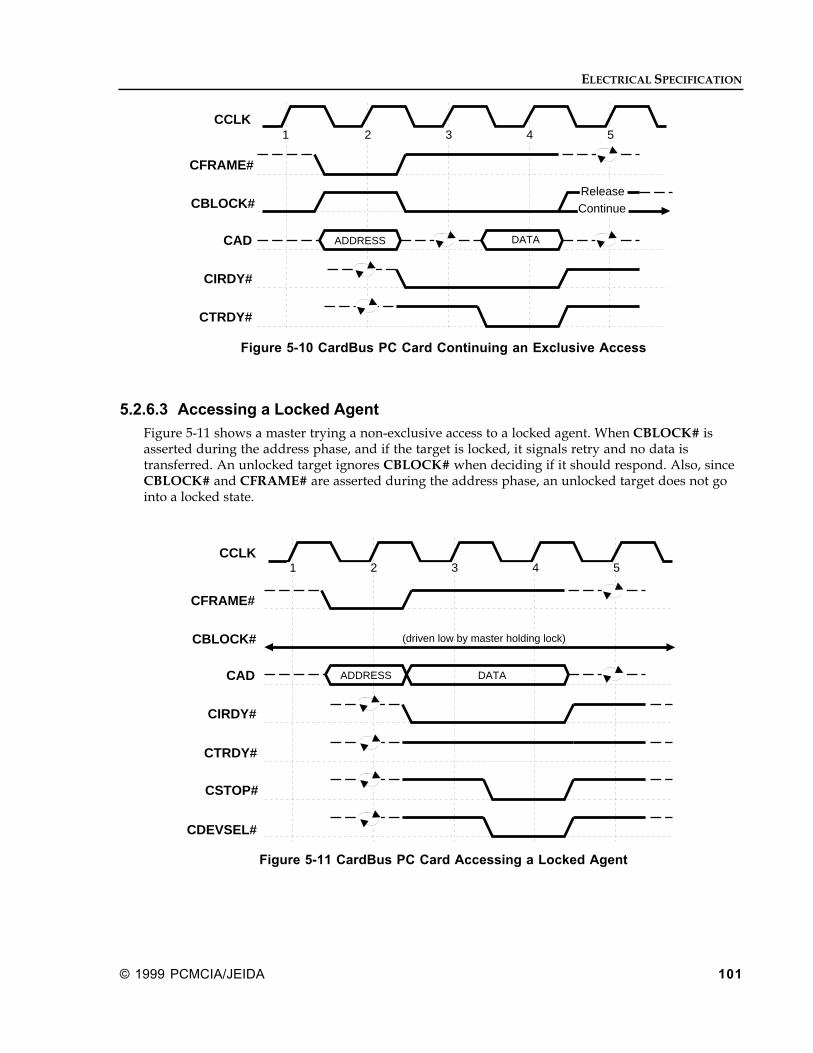
ELECTRICAL SPECIFICATION
© 1999 PCMCIA/JEIDA 101
CCLK
CFRAME#
CAD
CBLOCK#
CIRDY#
CTRDY#
ReleaseContinue
ADDRESS DATA
1 2 3 54
Figure 5-10 CardBus PC Card Continuing an Exclusive Access
5.2.6.3 Accessing a Locked Agent
Figure 5-11 shows a master trying a non-exclusive access to a locked agent. When CBLOCK# isasserted during the address phase, and if the target is locked, it signals retry and no data istransferred. An unlocked target ignores CBLOCK# when deciding if it should respond. Also, sinceCBLOCK# and CFRAME# are asserted during the address phase, an unlocked target does not gointo a locked state.
CCLK
CFRAME#
CAD
CBLOCK#
ADDRESS DATA
CIRDY#
CTRDY#
(driven low by master holding lock)
CSTOP#
CDEVSEL#
1 2 3 54
Figure 5-11 CardBus PC Card Accessing a Locked Agent

CARDBUS PC CARD ELECTRICAL INTERFACE
102 ©1999 PCMCIA/JEIDA
5.2.6.4 Completing an Exclusive Access
During the final transfer of an exclusive operation, CBLOCK# is negated so the target will acceptthe request, and then re-asserted until the exclusive access terminates successfully. The master maynegate CBLOCK# at anytime when the exclusive operation has completed. However, it isrecommended (but not required) that CBLOCK# be negated with the negation of CIRDY#following the completion of the last data phase of the locked operation. Releasing CBLOCK# at anyother time may result in a subsequent transaction being terminated with retry unnecessarily. Alocked agent unlocks itself whenever CBLOCK# and CFRAME# are negated.
If a master wants to execute two independent exclusive operations on the bus, it must ensure aminimum of one clock between operations where both CFRAME# and CBLOCK# are negated. (Forexample, the fast back-to-back case depicted in Figure 5-7 (clock 3) would be illegal.) This ensuresany target locked by the first operation is released prior to starting the second operation. (An agentmust unlock itself when CFRAME# and CBLOCK# are both negated on one clock edge.)
5.2.6.5 Supporting CBLOCK# and Write-back Cache Coherency
The resource lock as described earlier has a potential of deadlock when the host system is using awrite-back cache. A deadlock may occur if software allows locks to cross a cache line boundary whenwrite-back caching is supported and a complete resource lock is used. An example of this potentialdeadlock is where the lock spans memory locations corresponding to the host system cache lines nand n+1. Cache line n+1 has been modified in the cache. A master establishes a resource (memory)lock by reading location corresponding to cache line n. The locked operation continues by readinglocation corresponding to cache line n+1. The snoop (of n+1) results in a hit to modified line in thehost system's write-back cache. However, the cache writeback of the modified line fails because thetarget only accepts accesses from the owner of CBLOCK#. This results in a deadlock because theread cannot occur until the modified line is written back and the writeback cannot occur untilCBLOCK# ownership is released.
5.2.6.6 Complete Bus Lock
The CardBus PC Card resource lock can be converted into a complete bus lock by having the arbiternot grant the bus to any other agent while CBLOCK# is asserted. When the first access of the lockedsequence is retried, then the master must negate both its CREQ# and CBLOCK#. When the firstaccess completes normally, then the complete bus lock has been established and the arbiter will notgrant the bus to any other agent. If the arbiter granted the bus to another agent when the completebus lock was being established, the arbiter must remove the other grant to ensure that complete buslock semantics are observed. A complete bus lock may have a significant impact on the performanceof the system, particularly the video subsystem. All non-exclusive accesses will not proceed while alocked operation is in progress.
As with the complete resource lock and write-back cacheable memory, potential of a deadlock existsfor complete bus lock. The arbiter that supports complete bus lock must grant the bus to the cache toperform a writeback due to a snoop to a modified line when a lock is in progress.
5.2.7 Other Bus Operations
5.2.7.1 Device Selection
CDEVSEL# is driven by the target of the current transaction as shown in Figure 5-12. CDEVSEL#may be driven one, two, or three clocks following the address phase and its timing is indicated in

ELECTRICAL SPECIFICATION
© 1999 PCMCIA/JEIDA 103
the configuration space Status register. CDEVSEL# must be asserted with or prior to the edge atwhich the target enables its CTRDY#, CSTOP#, or data (read). In other words, a target must assertCDEVSEL# (claim the transaction) before it is allowed to issue any other target response. In all casesexcept one, once a target asserts CDEVSEL# it must not negate CDEVSEL# until CFRAME# isnegated (CIRDY# is asserted) and the last data phase has completed. With normal mastertermination, CDEVSEL# negation must be coincident with the negation of CTRDY#. The exceptionis the target-abort.
CTRDY#
CDEVSEL#
CIRDY#
CCLK
CFRAME#
NO RESPONSE
ACKNOWLEDGEFAST MED SLOW SUB
1 2 3 4 5 6 7 8
Figure 5-12 CDEVSEL# Assertion
If no agent asserts CDEVSEL# within three clocks of CFRAME#, the agent doing subtractive decodemay claim and assert CDEVSEL#. If the system does not have a subtractive decode agent, themaster never sees CDEVSEL# asserted and terminates the transaction per the master-abortmechanism (refer to 5.2.3.3.1 Master Initiated Termination).
A target must do a full decode before driving/asserting CDEVSEL#, or any other target responsesignal. It is illegal to drive CDEVSEL# prior to a complete decode and then let the decodecombinationally resolve on the bus. (This could cause contention.) A target must qualify the CADlines with CFRAME# before CDEVSEL# can be asserted on commands other than configuration. Atarget must qualify CCBE# and CAD[1::0] with CFRAME# before CDEVSEL# can be asserted on aConfiguration command.
It's expected that most (perhaps all) target devices will be able to complete a decode and assertCDEVSEL# within one or two clocks of CFRAME# being asserted (fast and medium in the figure).
Once CDEVSEL# has been asserted, it cannot be negated until the last data phase has completed,except to signal target-abort.
If the first access maps into the targets address range, it asserts CDEVSEL# to claim the access. But ifthe master attempts to continue the burst access across the resource boundary, the target is requiredto signal disconnect.
When a target claims an I/O access, and the byte enables indicate one or more bytes of the accessare outside the target's address range, it must signal target-abort. To deal with this type of I/Oaccess problem, a subtractive decode device (e.g., expansion bus bridge) may do one of thefollowing:
• do positive decode (by including a byte map) on addresses for which different devices sharecommon DWORDs, additionally using byte enables to detect this problem and signal target-abort.

CARDBUS PC CARD ELECTRICAL INTERFACE
104 ©1999 PCMCIA/JEIDA
• pass the full access to the expansion bus, where the portion of the access that cannot be servicedwill be ignored. (This occurs only when first addressed target resides on the expansion bus andthe other is on CardBus PC Card.)
5.2.7.2 Special Cycle
The Special Cycle command provides a simple message broadcast mechanism on CardBus PC Card.In addition to communicating processor status, it may also be used for logical sideband signalingbetween CardBus PC Card agents, when such signaling does not require the precise timing orsynchronization of physical signals.
A good paradigm for the Special Cycle command is that of a "logical wire" which only signals singleclock pulses; i.e., it can be used to set and reset flip flops in real time, implying that delivery isguaranteed. This allows the designer to define necessary sideband communication withoutrequiring additional pins. As with sideband signaling in general, implementation of Special Cyclecommand support is optional.
The Special Cycle command contains no explicit destination address, but is broadcast to all agents.Each receiving agent must determine whether the message is applicable to it. CardBus PC Cardagents will never assert CDEVSEL# in response to a Special Cycle command. This means that thereis no target handshaking of any kind on these transactions, and subtractive decoding bridges mustnot pass this bus operation on to their secondary bus. Special Cycle commands will not propagateacross bridges.
A Special Cycle command may contain optional, message dependent data, which is not interpretedby the CardBus PC Card interface itself, but is passed, as necessary, to the hardware applicationconnected to the CardBus PC Card interface. In most cases, explicitly addressed messages should behandled in one of the three physical address spaces on CardBus PC Card, and not with the SpecialCycle command.
Using a message dependent data field can break the logical wire paradigm mentioned above, andcreate delivery guarantee problems. However, since targets only accept messages they recognizeand understand, the burden is placed on them to fully process the message in the minimumdelivery time (six bus clocks) or to provide any necessary buffering for messages they accept.Normally this buffering is limited to a single flip flop. This allows delivery to be guaranteed. Insome cases it may not be possible to buffer or process all messages that could be received. In thiscase there is no guarantee of delivery.
A Special Cycle command is like any other bus command where there is an address phase and adata phase. The address phase starts like all other commands with the assertion of CFRAME# andcompletes like all other commands when CFRAME# and CIRDY# are negated. The uniqueness ofthis command compared to the others is that no agent responds with the assertion of CDEVSEL#.This command is basically a broadcast to all agents, and interested agents accept the command andprocess the request.
The address phase contains no valid information other than the command field. There is no explicitaddress. However, CAD[31::00] are driven to a stable level and parity is generated. During thedata phase CAD[31::00] contain the message type and an optional data field. The message isencoded on the least significant sixteen lines namely CAD[15::00]. The optional data field is encodedon the most significant sixteen lines namely CAD[31::16] and is not required on all messages. Themaster of a Special Cycle command can insert wait states like any other command while the targetcannot (since there is no explicit target). The message and associated data are only valid on the firstclock CIRDY# is asserted. The information contained in and the timing of subsequent data phases ismessage dependent.

ELECTRICAL SPECIFICATION
© 1999 PCMCIA/JEIDA 105
During the address phase, CCBE[3::0]# = 0001 (Special Cycle) and CAD[31::00] are driven torandom values and must be ignored. During the data phase, CCBE[3::0]# are asserted andCAD[31::00] are as follows:
CAD[15::00] Encoded message
CAD[31::16] Message dependent (optional) data field
The CardBus PC Card bus sequencer starts this command like all others and terminates it with amaster-abort. The hardware application provides all the information like for any other commandand starts the bus sequencer. When the sequencer reports that the access terminated with a master-abort, the hardware application knows the access completed. In this case, the Received Master Abortfield in the configuration space Status register must not be set. The quickest a Special Cyclecommand can complete is five clocks. One additional clock is required for the turnaround cyclebefore the next access. Therefore, a total of six CardBus PC Card clocks is required from thebeginning of a Special Cycle to the beginning of another access.
There are 64 KBytes of messages. The message encodings are defined and described in AppendixA.
5.2.7.3 Address/Data Stepping
The ability of an agent to spread assertion of qualified signals over several clocks is referred to asstepping. This notion allows an agent with weak output buffers to drive a set of signals to a validstate over several clocks (continuous stepping), thereby reducing the ground current load generatedby each buffer. An alternative approach allows an agent with strong output buffers to drive a subsetof them on each of several clock edges until they are all driven (discrete stepping), thereby reducingthe number of signals that must be switched simultaneously.
Either approach allows an agent to trade off performance for cost (fewer power/ground pins). Whenusing the continuous stepping approach, care must be taken to avoid mutual coupling betweencritical control signals that must be sampled on each clock edge and the stepped signals that may betransitioning on a clock edge.
Stepping is only permitted on CAD[31::00] and CPAR because they are always qualified by controlsignals; i.e., these signals are only considered valid on clock edges for which they are qualified.CAD's are qualified by CFRAME# in address phases, and by CIRDY# or CTRDY# in data phases(depending on which direction data is being transferred). CPAR is implicitly qualified on each clockafter which CAD was qualified.
Figure 5-13 illustrates a master delaying the assertion of CFRAME# until it has successfully drivenall CAD lines. The master is both permitted and required to drive CAD and CCBE# onceownership has been granted and the bus is IDLE. But it may take multiple clocks to drive a validaddress before asserting CFRAME#. However, by delaying assertion of CFRAME#, the masterruns the risk of losing its turn on the bus. As with any master, CGNT# must be asserted on theclock edge before CFRAME# is asserted. If CGNT# were negated, on the clock edges marked A,the master is required to immediately High-Z its signals because the arbiter has granted the bus toanother agent. (The new master would be at a higher priority level.) If CGNT# were negated onthe clock edges marked B or C, CFRAME# will have already been asserted, and the transactioncontinues.

CARDBUS PC CARD ELECTRICAL INTERFACE
106 ©1999 PCMCIA/JEIDA
CFRAME#
CCLK
CAD
CGNT#
CIRDY#
BE#'s-0CCBE#
1 2 3 4 5 6 7 8 9
ADDRESS DATA-0
A A CB
BUS CMD
Figure 5-13 Address Stepping
5.2.7.4 Configuration Cycle
The CardBus PC Card definition provides for totally software driven initialization and configurationvia a separate configuration address space. CardBus PC Card devices are required to provide 256bytes of configuration space for this purpose. Register descriptions are provided in the CardBus PCCard Programming Model section of this specification. This section describes the bus commands foraccessing the CardBus PC Card configuration space.
As previously discussed, each device decodes its own addresses for normal accesses. However,accesses in the configuration address space require device selection decoding to be done by the hostCardBus PC Card adapter. The configuration read and write cycle signals and timing are the sameas for other read and write commands. A CardBus PC Card device is a target of a configurationcommand (read or write) only if CAD[1::0] are 00 during the address phase of the command.Internal addressing of the 64-DWORD register space is done by CAD[7::2] and the byte enables.The Configuration command, like other commands, allows accesses of a byte, word, DWORD, or asa burst operation. The rest of the transaction is the same as other commands, including alltermination semantics. If no agent responds, the request is terminated via master-abort (refer to5.2.3.3.1 Master Initiated Termination).

ELECTRICAL SPECIFICATION
© 1999 PCMCIA/JEIDA 107
To support hierarchical buses, two types of configuration access are used. They have the followingformats which show the interpretation of CAD lines during the address phase of a configurationaccess:
BusNumber
FunctionNumber
RegisterNumber 0 0Reserved
01278101131
Type 0
FunctionNumber
RegisterNumber 0 1Reserved
01278101131
Type 1
DeviceNumber
15162324
Figure 5-14 Type 0 and Type 1 Configuration Accesses
Type 1 and Type 0 configuration accesses are differentiated by the values on the CAD[1::0] pins. AType 0 configuration cycle (when CAD[1::0] = "00") is used to select a device on the bus where thecycle is being run. A Type 1 configuration cycle (when CAD[1::0] = "01") is used to pass aconfiguration request on to another bus.
The Register Number and Function Number fields have the same meaning for both configurationtypes, while Device Number and Bus Number are used only in Type 1 accesses. Reserved fieldsmust be ignored by targets.
Table 5Ð6 Common Access Field Definitions
Register Number is an encoded value used to index a DWORD in configuration space of the intended target.
Function Number is an encoded value used to select one of eight possible functions on a device.
Device Number is an encoded value used to select 1 of 32 devices on a given bus.
Bus Number is an encoded value used to select 1 of 256 buses in a system.
Bridges (e.g., Host-to-CardBus PC Card) that need to generate a Type 0 configuration cycle use theDevice Number to select a CardBus PC Card device. The Function Number is provided onCAD[10::08]. The Register Number is provided on CAD[7::2]. CAD[1::0] must be 00 for a Type 0configuration access.
Type 0 configuration accesses are not propagated beyond the local CardBus PC Card and must beclaimed by a local device or terminated with master-abort.
If the target of a configuration access resides on another bus (not the local CardBus PC Card), a Type1 configuration access must be used. Type 1 accesses are ignored by all targets except CardBus PCCard-to-CardBus PC Card bridges. These devices decode the Bus Number field to determine if thedestination of the configuration access is residing behind the bridge. If the Bus Number is not for abus behind the bridge, the access is ignored. The bridge claims the access if the access is to a busbehind the bridge. If the Bus Number is not to the secondary bus of the bridge, the access is simplypassed through unchanged. If the Bus Number matches the secondary bus number, the bridgeconverts the access into a Type 0 configuration access. The bridge changes CAD[1::0] to 00 andpasses CAD[10::02] through unchanged. The Device Number is decoded to select one of 32 deviceson the local bus, and the bridge initiates a configuration access to that device.

CARDBUS PC CARD ELECTRICAL INTERFACE
108 ©1999 PCMCIA/JEIDA
Devices that respond to Type 0 configuration cycles are separated into two classes. The first class(single function device) uses only CAD[1::0] (00) to determine whether or not to respond. Thesecond class of device (multi-function device) understands the Function Number field and usesCAD[1::0] (00), as well as the encoded value on CAD[10::08] to determine whether or not torespond. The two classes are differentiated by an encoding in the configuration space header.
Multi-function devices are required to do a full decode on CAD[10::08], and only respond to theconfiguration cycle if they have implemented the configuration space registers for the selectedfunction. They are also required to always implement function 0 in the device. Implementing otherfunctions is optional and may be assigned in any order (i.e., a two-function device must respond tofunction 0, but can choose any of the other possible function numbers (1-7) for the second function).
Configuration code will probe the bus in Device Number order (i.e., Function Number will bezero). If a single function device is detected, no more functions for that Device Number will bechecked. If a multi-function device is detected, then all remaining Function Numbers will bechecked.
5.2.7.4.1 Generating Configuration Cycles
Systems must provide a mechanism that allows CardBus PC Card configuration cycles to begenerated by software. This mechanism is typically located in the host bridge or the host CardBusPC Card adapter. For PC-AT compatible systems, the mechanism for generating configurationcycles is defined and specified below. For other system architectures there is presently nospecification.
Host bridges and host CardBus PC Card adapters to be used in PC-AT compatible systems mustimplement this mechanism for generating CardBus PC Card configuration cycles.
5.2.7.4.1.1 Configuration Mechanism
Two DWORD I/O locations are used in this mechanism. The first DWORD location (CF8H)references a read/write register that is named CONFIG_ADDRESS. The second DWORD address(CFCH) references a register named CONFIG_DATA. The general mechanism for accessingconfiguration space is to write a value into CONFIG_ADDRESS that specifies a particular CardBusPC Card in the system, device on that bus, and configuration register in that device being accessed.A read or write to CONFIG_DATA will then cause the bridge to translate that CONFIG_ADDRESSvalue to the requested configuration cycle on that CardBus PC Card.
DeviceNumber
FunctionNumber
RegisterNumber 0 0Reserved
01278101130
BusNumber
1516232431
Enable bit (Ô1Õ = enabled, Ô0Õ = disabled)
Figure 5-15 Layout of CONFIG_ADDRESS Register
The CONFIG_ADDRESS register is 32 bits with the format shown in Figure 5-15 Figure. Bit 31 is anenable flag for determining when accesses to CONFIG_DATA should be translated to configurationcycles on CardBus PC Card. Bits 30 to 24 are reserved, read-only, and must return 0's when read.Bits 23 through 16 choose a specific CardBus PC Card bus in the system. Bits 15 through 11 choose aspecific device on the bus. Bits 10 through 8 choose a specific function in a device (if the devicesupports multiple functions). Bits 7 through 2 choose a DWORD in the device's configuration space.Bits 1 and 0 are read-only and must return 0's when read.

ELECTRICAL SPECIFICATION
© 1999 PCMCIA/JEIDA 109
Anytime a host bridge sees a full DWORD I/O write to CONFIG_ADDRESS, the bridge must latchthe data into its CONFIG_ADDRESS register. On full DWORD I/O reads to CONFIG_ADDRESS,the bridge must return the data in CONFIG_ADDRESS. Any other types of accesses to this address(non-DWORD) must be treated like a normal I/O access and no special action should be taken.Therefore, the only I/O space consumed by this register is a DWORD at the given address. I/Odevices using BYTE or WORD registers are not affected because the cycles will be passed onunchanged.
When a bridge sees an I/O access that falls inside the DWORD beginning at CONFIG_DATAaddress, it checks the enable bit and the BUS NUMBER in the CONFIG_ADDRESS register. Ifconfiguration cycle translation is enabled and the BUS NUMBER matches the bridge's bus numberor any bus number behind the bridge, then a configuration cycle translation must be done.
There are two types of translation that take place. The first, Type 0, is a translation where the devicebeing addressed is on the CardBus PC Card bus connected to the bridge. The second, Type 1, occurswhen the device is on another bus somewhere behind this bridge.
For Type 0 translations (see Figure 5-16), the bridge does a decode of the Device Number field toaccess the appropriate device15 and performs a configuration cycle on CardBus PC Card, whereCAD[1::0] is 00. Bits 10 - 8 of CONFIG_ADDRESS are copied to CAD[10::8] on CardBus PC Card asan encoded value which may be used by components which contain multiple functions. CAD[7::2]are also copied from the CONFIG_ADDRESS register. Figure 5-16 shows the translation from theCONFIG_ADDRESS register to CAD lines on CardBus PC Cards.
ReservedBus
NumberDeviceNumber
FunctionNumber
RegisterNumber
0 0
012781011151623243031
CONFIG_ADDRESSREGISTER
Undefined 0 0
01101131
CardBus PC CardCAD LINES
Selects a CardBus PC Card
Figure 5-16 Bridge Translation for Type 0 Configuration Cycles
For Type 1 translations, the bridge directly copies the contents of the CONFIG_ADDRESS registeronto the CardBus PC Card CAD lines during the address phase of a configuration cycle makingsure that CAD[1::0] is 01.
In both cases, byte enables for the data transfers must be directly copied from the processor bus.
For systems with peer bridges on the processor bus, one peer bridge would typically be designatedto always handshake accesses to the CONFIG_ADDRESS register. Other bridges would snoop thedata written to this register. Accesses to the CONFIG_DATA register are typically handshaken bythe bridge doing the configuration translation.
15 If the Device Number field contains an invalid device number, the bridge must complete the processor access
normally, dropping the data on writes and returning all ones on reads.

CARDBUS PC CARD ELECTRICAL INTERFACE
110 ©1999 PCMCIA/JEIDA
Host bridges and CardBus PC Card-to-CardBus PC Card bridges typically require two configurationspace registers whose contents are used to determine when the bridge does configuration cycletranslation. One register (Bus Number) specifies the bus number of the CardBus PC Card directlybehind the bridge, and the other register (Subordinate Bus Number) specifies the number of the lasthierarchical bus behind the bridge.16 POST code is responsible for initializing these registers toappropriate values.
5.2.7.4.1.2 Generating Special Cycles with the Configuration Mechanism
This section defines how host bridges that implement the Configuration Mechanism for accessingconfiguration space should allow software to generate Special Cycles. Host bridges are not requiredto provide a mechanism for allowing software to generate Special Cycles.
When the CONFIG_ADDRESS register gets written with a value such that the Bus Number matchesthe bridge's bus number, the Device Number is all 1's, the Function Number is all 1's, and theRegister Number has a value of zero, then the bridge is primed to do a Special Cycle the next timethe CONFIG_DATA register is written. When the CONFIG_DATA register is written, the bridgegenerates a Special Cycle encoding (rather than configuration write) on the CCBE[3::0]# pins duringthe address cycle, and drives the data from the I/O write onto CAD[31::00] during the first datacycle. Reads to CONFIG_DATA, after CONFIG_ADDRESS has been set up this way, haveundefined results. The bridge can treat it as a normal configuration cycle operation (i.e. generate aType 0 configuration cycle on CardBus PC Card). This will terminate with a master-abort and theprocessor will have all 1's returned.
If the Bus Number field of CONFIG_ADDRESS does not match the bridge's bus number, then thebridge passes the write through CONFIG_DATA on to CardBus PC Card as a Type 1 configurationcycle just like anytime the bus numbers don't match.
5.2.8 Error FunctionsCardBus PC Card provides for parity and other system errors to be detected and reported. CardBusPC Card error coverage may range from devices that have no interest in errors (particularly parityerrors) to agents that detect, signal, and recover from errors. This allows agents that recover fromparity errors to avoid affecting the operation of agents that do not. To allow this range of flexibility,the generation of parity is required on all transactions by all agents. The detection and reporting oferrors is also required.
The discussion of errors is divided into the following two sections covering parity generation anddetection, and error reporting. Each section explains what is optional and what is required for eachfunction.
5.2.8.1 Parity
Parity on CardBus PC Card provides a mechanism to determine transaction by transaction if themaster is successful in addressing the desired target and if the data transfer occurred correctly. Toensure that the correct bus operation is performed, the four command lines are included in theparity calculation. To ensure that correct data is transferred, the four byte enables are also includedin the parity calculation. The agent that is responsible for driving CAD[31::00] on any given busphase is also responsible for driving even parity on CPAR.
During address and data phases, parity covers the CAD[31::00] and CCBE[3::0]# lines regardless ofwhether or not all lines carry meaningful information. Byte lanes not actually transferring data are
16 Host bridges that do not allow peer bridges do not need either of these registers since the bus behind the bridge is,
by definition, bus 0 and all other CardBus PC Card buses are subordinate to bus 0.

ELECTRICAL SPECIFICATION
© 1999 PCMCIA/JEIDA 111
still required to be driven with stable (albeit meaningless) data and are included in the paritycalculation. During Configuration or Special Cycle commands, some (or all) address lines are notdefined but are required to be driven to stable values and are included in the parity calculation.
Parity is generated according to the following rules:
• Parity is calculated in the same way on all CardBus PC Card transactions regardless ofthe type or form.
• The number of "1"s on CAD[31::00], CCBE[3::0]#, and CPAR equals an even number.
• Parity generation is not optional; it must be done by all CardBus PC Card compliantdevices.
On any given bus phase, CPAR is driven by the agent that drives CAD[31::00] and lags thecorresponding address or data by one clock. Figure 5-17 illustrates a read and write transaction withparity. The master drives CPAR for the address phases on clock 3 and 7. The target drives CPARfor the data phase on the read transaction (clock 5) while the master drives CPAR for the data phaseon the write transaction (clock 8). Note that other than the one clock lag, CPAR behaves exactly likeCAD[31::00] including wait states and turnaround cycles.
CFRAME#
CCLK
CAD
CPAR
CPERR#
1 2 3 4 5 6 7 8 9
ADDRESS DATA ADDRESS DATA
Figure 5-17 Parity Operation
Parity must be checked to determine if the master successfully addressed the desired target and ifdata transferred correctly. Checking of parity on CardBus PC Card is required except in one class ofdevices listed in 5.2.8.2 Error Reporting. Agents that support parity checking must always set theDetected Parity Error field in the configuration space Status register when a parity error is detected.Any additional action beyond setting this field is conditional upon the Parity Error Response field inthe configuration space Command register and is discussed in the error reporting section.
Any agent may check and signal an address parity error on CSERR#. Only the master may reporta read data parity error and only the selected target may signal a write data parity error.
5.2.8.2 Error Reporting
As mentioned, CardBus PC Card provides for the detection and signaling of both parity and othersystem errors. It is intended that parity errors be reported up through the access and device driverchain whenever possible. This error reporting chain from target to bus master to device driver todevice manager to operating system is intended to allow error recovery options to be implementedat any level. Since it is generally not possible to associate system errors with a specific access chain,they are reported directly to the system level.

CARDBUS PC CARD ELECTRICAL INTERFACE
112 ©1999 PCMCIA/JEIDA
Two signals are used in the CardBus PC Card error reporting scheme. CPERR# is used exclusivelyfor reporting data parity errors on all transactions except Special Cycle commands. It is a sustainedtri-state signal and is bussed to all CardBus PC Card agents. Bus protocol assures that CPERR# willnever be simultaneously driven by multiple bus agents and that proper signal turn around timesare observed to avoid any driver contention.
CSERR# is used for other error signaling, including address parity, and data parity on SpecialCycle commands, and may optionally be used on any other non-parity or system errors. It is anopen drain signal that is wire-ORÕed with all other CardBus PC Card agents and, therefore, may besimultaneously driven by multiple agents. Since open drain signaling cannot guarantee stablelevels on every clock edge, once CSERR# is asserted its logical value must be assumed to beindeterminate until the signal is sampled in the negated state on at least two successive clock edges.
Both CPERR# and CSERR# are required pins since parity error signaling on CardBus PC Card isrequired. Note that all agents are required to generate parity.
Use of CSERR# to signal non-parity errors is optional. It must be assumed, however, that signalingon CSERR# will generate an NMI and is, therefore, fatal. Consequently, care should be taken inusing CSERR#.
The following sections cover the responsibility placed on each bus agent regarding signaling on theCPERR# and CSERR# pins.
5.2.8.2.1 Parity Error Response and Reporting on CPERR#
This section describes proper response to, and reporting of, data parity errors in all bus operationsexcept Special Cycle commands. All address parity errors, as well as Special Cycle command dataparity errors are reported on the CSERR# signal, and are described in the next section. Allreferences to parity errors in this section are by implication limited strictly to data parity (exceptSpecial Cycle commands).
CardBus PC Card uses the CPERR# pin to signal a data parity error between connected devices onCardBus PC Card (except on Special Cycle commands). Only the master of a corrupted data transferis allowed to report parity errors to software, using mechanisms other than CPERR#. Targets alwayssignal data parity errors back to the master on CPERR#. This gives the originator of the access, ateach hardware or software level, the prerogative of recovery.
Except for setting the Parity Error Detected field, all parity error signaling and response iscontrolled by the Parity Error Response field. This field is required except in the previously listed(excluded) devices. If the field is cleared, the agent ignores all parity errors and completes thetransaction as though parity was correct. If the field is set, the agent is required to assert CPERR#when a parity error is detected; additional error response is device dependent. In all cases, theDetected Parity Error field must be set.
An agent must always assert CPERR# two CardBus PC Card clocks after a data transfer in which anerror occurred, as shown in Figure 5-17. The agent receiving data is free to assert CPERR# when aparity error is detected (which may occur before data is transferred).17 Once CPERR# is asserted, itmust remain asserted until two clocks following the actual transfer. A master knows a data parityerror occurred anytime CPERR# is asserted but only knows the transfer was error free two clocksfollowing the transfer.
In the case of multiple data transfers without intervening wait states, CPERR# will be qualified onmultiple consecutive clocks accordingly, and may be asserted in any or all of them. Since CPERR#is a sustained tri-state signal, it must be actively driven to the correct value on each qualified clock
17 On a write transaction, this can occur when CIRDY# is asserted and the target is inserting wait states. On a read
transaction, this occurs when CTRDY# is asserted and the master is inserting wait states.

ELECTRICAL SPECIFICATION
© 1999 PCMCIA/JEIDA 113
edge. To return it to nominal state at the end of each bus operation, it must be actively driven highfor one clock period, starting two clocks after the CAD bus turnaround cycle (e.g., clock 7 in Figure5-17.) The CPERR# turnaround cycle occurs one clock later (clock 8 in Figure 5-17.) CPERR# maynever be driven (enabled) for the current cycle until at least three clocks after the address phase.
When a master detects a data parity error and asserts CPERR# (on a read transaction) or samplesCPERR# asserted (on a write transaction) it must set the Data Parity Detected field (Status register,bit 8), and can either continue the transaction or terminate it. A target of a transaction that detects aparity error can either continue the operation or cause it to be stopped via target termination.Targets never set the Data Parity Reported field. When CPERR# is asserted, it is recommended thatboth the master and target complete the transaction. CPERR# is only an output signal for targetswhile masters use CPERR# as both an input and output.
When the master of the access becomes aware that a parity error has occurred on its transaction, it isrequired to inform the system. It is recommended that the master inform its device driver of theerror by generating an interrupt (or modifying a status register or flag to mention a few options). Ifnone of these options is available to the device, it may, as a last recourse, pass responsibility of theerror to the operating system by asserting CSERR#. Note that the system designer may elect toreport all parity errors to the operating system by converting all CPERR# error signals intoCSERR# error signals in the central resource.
5.2.8.2.2 Error Response and Reporting on CSERR#
CSERR# is used to signal all address parity errors, data parity errors on Special Cycle commands(since these are broadcast writes), and all errors other than parity errors. Any agent can check andsignal address parity errors on CSERR#, regardless of intended master and target. CSERR# mayonly be asserted when the SERR Enable field in the Command register is set to a logical one (high),regardless of the error type. When an agent asserts CSERR# it is required to set the SignaledSystem Error field in the configuration space Status register, regardless of the error type. Inaddition, if the error type is parity (e.g., address parity), the Parity Error Detected field must be setin all cases, but reporting on CSERR# is conditioned on the Parity Error Response field in theCommand register.
A selected agent that detects an address parity error should do one of the following:claim the transaction and terminate with target-abort, or not claim the cycle and let it terminate withmaster-abort. The target is not allowed to terminate with retry or disconnect because an addressparity error was detected.
CSERR# has no timing relationship to any CardBus PC Card transaction.18 However, errors shouldbe signaled as quickly as possible, preferably within two clocks of detection. The only agentinterested in CSERR# (as an input) is the central resource that converts a low pulse into a signal tothe processor. How the central resource signals the processor is system dependent, but could includegenerating an NMI, high priority interrupt, or setting a status field or flag. However, the agent thatasserts CSERR# must be willing for the central resource to generate an NMI. Otherwise, the errorshould be reported by a different mechanism (e.g., an interrupt, status register, or flag).
When the Parity Error Response field is enabled, and the SERR Enable field enabled, an agent mayassert CSERR# under the following conditions:
• Address parity error, or data parity error on Special Cycles detected.
• The detection of a parity error that is not reported by some other mechanism (current busmaster only).
18 Except for CCLK .

CARDBUS PC CARD ELECTRICAL INTERFACE
114 ©1999 PCMCIA/JEIDA
When the SERR Enable field is enabled, an agent may assert CSERR# under the followingconditions:
• The master (which does not have a driver) was involved in a transaction that was abnormallyterminated.
• A catastrophic error that left the agent questioning its ability to operate correctly.
Note that master-abort is not an abnormal condition for bridges during Configuration and SpecialCycle commands. CSERR# should not be used for these conditions or for normally recoverablecases. The assertion of CSERR# should be done with deliberation and care since the result may bean NMI. Target-abort is generally an abnormal target termination and may be reported (only bythe master) as an error by signaling CSERR# when the master cannot report the error through itsdevice driver.
5.2.9 Cache SupportIn a mobile or a small desktop system, part or all of the system memory may reside on CardBus PCCard. This may include read only program modules as well as RAM, both of which must becacheable by the processor. Also, supporting XIP (eXecute In Place) of software stored on PC Cardsis an important part of the CardBus PC Card standard. To make XIP viable, the XIP memory on PCCards must be cacheable, otherwise the execution performance would suffer considerably. However,supporting cacheability of the memory residing on PC Cards, and providing a mechanism formaintaining the memory and processor cache's data consistency involves some system and CardBusPC Card interface design trade offs. CardBus PC Cards may contain cacheable memory. Thecacheability rules are optimized for systems using removable PC Cards.
The CardBus PC Card memory caching option assumes:
• A consistent, common, flat physical address space is maintained in the system, i.e. a givenaddress has a unique destination and an access of that address produces the same resultsregardless of the access origin. This allows for the host system and bus masters on PC Cards toaccess the system memory and memory on PC Cards, any memory mapped into the commonaddress space, in a uniform way.
Note that this provision does not preclude some private memory spaces in the host system or onPC Cards. Also note that special memory mapping cases, like the DOS Compatibility Hole, areoutside the scope of this specification.
• The host system, the system master, is responsible for memory mapping and memoryallocation, including the memory on PC Cards.
• The host system's cache coherency must be maintained as if agents on the bus master cardswould be accessing the host system memory.
The first two rules for caching memory in the CardBus PC Card environment (and in the system)are generic. They are as following:
1. An agent's private memory is not a shared memory, and, in general, it is not visible to otheragents in the system. It is cacheable by the corresponding agent without any limitationspertaining to presence of CardBus PC Card in the system. An agent (a device or a function ofthe device) can cache its own private memory. This memory must not be shared with otheragents (devices) in the system. The agent is responsible for maintaining its cache and memorydata consistency.
2. Non-modifiable code or data (ROM) can be cacheable, providing that corresponding code ordata in the cache(s) is write protected. If an agent cannot guarantee write protection of thecached ROM data in its own cache, then this data is not cacheable by that agent.

ELECTRICAL SPECIFICATION
© 1999 PCMCIA/JEIDA 115
For a read/write shared memory on PC Cards, the following cacheability discipline and requirementsmust be met:
1. The host system may cache memory on a CardBus PC Card if the card configuration allows it(e.g., as set in the card's Configuration Space), with hardware maintained data consistency.
2. All accesses to memory Cacheable by the host system must be visible to the host system formaintaining its cache coherency.
3. An agent on a CardBus PC Card may cache only the card's on-board (local19) memory. If theagent on the CardBus PC Card caches its local memory, that memory must not be cacheable bythe host system (e.g., disallowed in the card's Configuration Space). Cacheability of the card'smemory by the host system or by the local agent must be configured by the host system duringinitialization of the card.
4. If an agent on the CardBus PC Card caches its local memory, it is responsible for its cache andthe memory data consistency when any other agent accesses that local memory.
In general, if the CardBus PC Card and the system bus do not operate concurrently, all CardBus PCCard addresses should be visible on the system bus. Otherwise, the host CardBus PC Card adaptermust forward addresses in the cacheable range to the system bus for snooping. Also, card's addressrange(s) which represent memory mapped I/O are not cacheable, while other regions of the card'smemory might be cacheable.
Any function in a CardBus PC Card device that contains memory that might be cacheable by thehost system, must implement a writable Cache Line Size register (refer to the CardBus PC CardProgramming Model Section of this specification). Contents of this register cannot be hard-wired toany value. It must be written by the host system during the function configuration. If a non-zerovalue is written into the Cache Line Size register, the agent must disconnect all types of memorytransactions (all Memory commands) crossing the cache line boundaries. If zero value is written tothe Cache Line Size register, the agent is released from maintaining the memory caching discipline,i.e. it does not have to disconnect CardBus PC Card transactions on the cache line boundaries.
If the Cache Line Size register is written to 0, it is the responsibility of the host system software tomaintain the host system's cache coherency with respect to the memory on the card, or disablecaching of that memory.
An agent containing memory that is not cacheable by the host system, may hard-wire the contentsof the Cache Line Size register to zero.
5.2.10 Clock Control
5.2.10.1 Clock Frequency
The host system is allowed to vary the CardBus PC Card clock frequency, implement a single,constant clock frequency, or stop the clock without software notification to CardBus PC Card devices.The host system can change the clock frequency only when the CardBus PC Card interface is idle.The clock (CCLK) can be stopped by the host system only while the CardBus PC Card interface isidle, and no bus request (CREQ#20) or lock (CBLOCK#) is asserted by a CardBus PC Card agent.The clock can be stopped only in a low state, and the clock line must remain low until the clock is
19 Private and local memory are not synonyms here. Private memory is not a shared memory. The term local (on-
board) memory designates physical memory location, e.g. on a PC Card with another CardBus PC Card agent.The local memory, however, could be logically shared by two or more agents in the system.
20CGNT# is not being considered here because it may never be asserted to a card unless the card's CREQ# isasserted. The CardBus PC Card central resource (e.g., the host CardBus PC Card adapter) is the default bus owner.
CARDBUS PC CARD ELECTRICAL INTERFACE
116 ©1999 PCMCIA/JEIDA
restarted. The minimum clock cycle time and the minimum clock high and low parameters mustnot be violated, and the clock edges must be monotonic. (See 5.3 CardBus PC Card ElectricalSpecification for the clock specifications).
The provisions for variable clock frequency and for stopping the interface clock require the CardBusPC Card device's interface logic to maintain its state. The device cannot rely on any particularfrequency of the clock across the interface.
5.2.10.2 Clock Control Protocol
The CardBus PC Card clock control protocol is implemented using an optional CCLKRUN# signal.
A PC Card asserts CCLKRUN# to request the host system:
• To restore the interface clock to a normal operating frequency21 if it is stopped or running belowthis frequency.
• To keep the clock running while an internal process on the card is in progress.
The host system drives the CCLKRUN# line as following:
• Negates CCLKRUN# to indicate that the clock is about to be stopped or slowed to a non-operational frequency. The host system should not negate CCLKRUN# if it is not going to stopor slow down the clock.
• Asserts CCLKRUN# when the interface clock is either: running at a normal operatingfrequency, or about to be started (or brought up to a normal operating frequency)
The CCLKRUN# signal is functional only while power on the CardBus PC Card interface is on.When the power is off, the CCLKRUN# line has no meaning.
A PC Card which does not implement the CCLKRUN# signal must leave this pin unconnected. Ahost system which does not implement this clock control protocol must always assert theCCLKRUN# signal.
Devices are not allowed to pulse CCLKRUN# continuously to indicate non-static implementation oftheir logic, thus preventing the host system from stopping the clock.
5.2.10.2.1 Clock Stop or Slow down
The host system (the CardBus PC Card adapter or the clock resource) drives CCLKRUN# low whileCCLK is running at a normal operating frequency (refer to Figure 5-18). Before stopping the clockor slowing the clock down to a non-operational frequency, the host system synchronously drivesCCLKRUN# high for one clock period, and then switches its driver to the High-Z state. A lowcurrent pull-up (a keeper) must be provided by the host system to prevent the line from floating.Implementations may disable the pull-up when the host system samples CCLKRUN# low.
CCLK continues to run unchanged for a minimum of four clock periods after CCLKRUN# isnegated. In addition, CCLK must not be stopped before the card can request it to continue byasserting CCLKRUN# (refer to 5.2.10.2.3 Maintaining the Interface Clock). For example, after clock8 (in the timing diagrams, Figure 5-18 and Figure 5-20), the host system may stop or slow down theclock if the requirements specified in 5.2.10.2.3 are met.
CardBus PC Card devices are required to maintain their states while the interface clock is stopped orthe clock frequency is changed.
21Normal operating frequency is any frequency at which transactions can be executed across the interface. It does not
necessarily mean the maximum CCLK frequency. It is up to the host's discretion to establish the operatingfrequency of the interface at a given time.

ELECTRICAL SPECIFICATION
© 1999 PCMCIA/JEIDA 117
CIRDY#
CCLK
CFRAME#
CCLKRUN#
DRIVEN BY HOST PULL-UP ENABLED
1 2 3 4 65 7 8 9
Figure 5-18 CardBus PC Card Clock Stop or Slow Down
5.2.10.2.2 Clock Restart or Speed up
To request restoration of the interface clock, a device asserts the CCLKRUN# signal asynchronously.The device holds CCLKRUN# asserted until it detects two rising edges of CCLK (refer to Figure 5-19 .) After the second clock edge, the device must disable its open drain driver.
After detecting the assertion of CCLKRUN#, the host system starts the clock if the clock wasstopped, or brings it to an operating frequency if the clock was slowed down.
The host system drives CCLKRUN# low at any time after it detects that the line is asserted by theCardBus PC Card device, but not later than on clock 3 (in the timing diagram, Figure 5-19 .) Thehost system may disable the pull-up on the CCLKRUN# line at this time.
The host system must not drive CCLKRUN# high earlier than on clock 5.
The device may not assert (start driving) CCLKRUN# if it is already driven low by the host system.The device must not assert CCLKRUN# unless the line has been negated for two successive clocks,e.g., before the clock was stopped.
It is expected that a device which has asserted CCLKRUN# for gaining bus mastership would assertCREQ# no later than four clocks after the clock is restarted. Otherwise, the clock can be stoppedagain by the host system.
The host system should provide low latency clock restoration to the interface upon assertion ofCCLKRUN# (typically, not more than a few cycles of its internal clock) since this latency wouldnegatively impact the interface performance. The intent of this protocol is to provide a low latencyclock control which is transparent to the host system software, and which would have no apparentimpact on the system performance.

CARDBUS PC CARD ELECTRICAL INTERFACE
118 ©1999 PCMCIA/JEIDA
CCLK
CCLKRUN#
CREQ#
PULL-UP ENABLED
DRIVEN BY CARD
DRIVEN BY HOST
1 2 3 4 5 6
Figure 5-19 CardBus PC Card Clock Start or Speed up
5.2.10.2.3 Maintaining the Interface Clock
Certain devices may require the interface clock to be active for completing some internal processesafter a CardBus PC Card transaction is already completed. This is accomplished by having thedevice assert CCLKRUN# after it has been negated for two successive CardBus PC Card clocks(refer to Figure 5-20.) The device must assert CCLKRUN# within a certain time window to avoidinterruption of the clock stream. In Figure 5-20 , the device samples CCLKRUN# high on clock 4,and must drive CCLKRUN# low no later than one Tval after clock 6, but not earlier than after theturn around cycle which occurs after clock 4. The device keeps CCLKRUN# asserted for two clocks(clocks 6 and 7, or clocks 7 and 8), and must disable its open drain driver after the second clock.
The host system must provide a non-interrupted clock when the device asserts CCLKRUN# in thetime specified above. The system designer should take into account:
1. All delays in the path to the systemÕs function controlling the clock and to the clock source.
2. The time required to synchronize CCLKRUN#. The clock resource must not stop the clockbefore a synchronized version of the CCLKRUN# signal received from the device can begenerated.
3. The host system must drive CCLKRUN# low on the CardBus PC Card interface no later than onclock 8. (The host system may drive the line low at any time after it detects that CCLKRUN# isasserted by the CardBus PC Card device.)
The host system must not drive CCLKRUN# high earlier than on the fourth clock edge after theCCLKRUN# line was first sampled asserted.
The device may not drive CCLKRUN# if it is already driven low by the host system. The devicemust not assert CCLKRUN# unless it has sampled the line high on a CCLK rising edge, and mustnot drive CCLKRUN# on the same clock edge on which the line is first sampled high.

ELECTRICAL SPECIFICATION
© 1999 PCMCIA/JEIDA 119
CCLKRUN#
DRIVEN BY HOST DRIVEN BY HOST
CFRAME#
CIRDY#
CCLK
PULL-UP ENABLED
DRIVEN BY CARD
1 2 3 4 5 6 7 8 9
Figure 5-20 Maintaining CardBus PC Card Clock
5.2.11 Status Changed Notification
5.2.11.1 Card Status Changed
Card Status Changed (CSTSCHG) is an optional signal which is used by PC Cards to notify the hostsystem about such events as changes in the Ready (READY), Write Protect (WP), or Battery VoltageDetect (BVD[2::1]) conditions of the card. (See 4.4.14 Status Changed (STSCHG#) [I/O and MemoryInterface].) CSTSCHG on CardBus PC Card is a level sensitive interrupt which is separate anddistinct from the functional interrupt CINT#. The CSTSCHG signal on CardBus PC Card is assertedhigh, unlike its 16-bit PC Card (STSCHG#) equivalent, and it is asynchronous to the CardBus PCCard clock.
Each function on a CardBus PC Card provides a set of four 32-bit registers: Function Event, FunctionEvent Mask, Function Present State, and Function Force Event. These registers are located inmemory space at the location given by the CISTPL_CONFIG_CB tuple in the function's CardInformation Structure (CIS). The order of the four 32-bit registers is: offset + 0: Function Event; offset+ 4: Function Event Mask; offset + 8: Function Present State; offset +12: Function Force Event. Fordescription of the registers, refer to 5.2.11.3 Register Descriptions.
These registers are sometimes optional in CardBus PC Cards that do not implement the CSTSCHGsignal. In that case, TPCC_ADDR (CISTPL_CONFIG_CB) must have the Address Space Indicatorfield set to zero (0) (see also the Metaformat Specification).
When the CSTSCHG signal is implemented these registers support Status Changed Notification.When the CINT# signal is implemented these registers support Functional Interrupt Notification.When neither CSTSCHG or CINT# signals are implemented these registers provide a consistentinterface to CardBus PC Card system software.
5.2.11.2 System and Interface Wake up
The CardBus PC Card specification defines an optional system and interface Wakeup protocol usingthe CSTSCHG line. This protocol allows a CardBus PC Card to request that the system powers upand configures the interface when the interface is powered off. When the interface is powered up,the CSTSCHG line is used to signal the Card Status Changed events.

CARDBUS PC CARD ELECTRICAL INTERFACE
120 ©1999 PCMCIA/JEIDA
When the CardBus PC Card interface is powered off, the power required to drive the CSTSCHGsignal must come from either an external source or from some power source on the card itself (e.g., alocal battery).
In its negated state, CSTSCHG signal is held low. When an external event occurs, the card drives asingle positive pulse on the CSTSCHG line. Optionally, the card may drive CSTSCHG as a highlevel or series of pulses until the interface is powered up (or until CRST# is negated by the hostsystem). Note that when the CardBus PC Card interface is powered up, the Status Changed issignaled on the CSTSCHG line as a level, not a pulse.
Battery powered cards assert the CSTSCHG signal for a minimum duration of 1 ms to minimizeenergy drain from on card batteries (especially when the host system is completely powered off ordoes not support the Wakeup protocol).
The host system, which implements this Wakeup protocol, must be able to latch a single CSTSCHGpulse of the minimum duration. The host system cannot rely on continuous assertion or series ofCSTSCHG pulses to be driven by the card when the interface is powered off.
The host system can mask the CSTSCHG signal on a particular card or on several cards using theFunction Event Mask register(s).
In order to prevent the system from spurious wake up due to the CSTSCHG signal during a powerdown process, the system must assert the CardBus PC Card reset (CRST#) before and throughoutpowering off the CardBus PC Card interface (See also 5.3.3.2 Reset and 5.5.4.7.2 CSTSCHGRequirements.)(see the CardBus PC Card Electrical Specification and the Requirements for Cards andSockets sections for CRST# parameters and power cycling requirements).
Upon detecting of the CSTSCHG signal assertion, the host system which supports this Wakeupprotocol is expected to:
• Return the system to an operational state
• Power up and configure the CardBus PC Card interface
The host system must assert the CardBus PC Card reset (CRST#) while powering up the interface.
After the interface is powered up and configured, the CSTSCHG line assumes its original CardStatus Changed signaling functionality.
The CSTSCHG signal driven by the card must be current-limited to prevent damage to the card orthe host system. The required signal parameters are specified in the CardBus PC Card ElectricalSpecification section.
A CardBus PC Card which uses the CSTSCHG line for a system and/or the interface wake up,must implement the Function Event, Function Event Mask, Function Present State and FunctionForce Event registers. Signaling Wakeup on the CSTSCHG line is allowed only if the Wakeup(WKUP) field is set and the mask field corresponding to the wake up event is set in the FunctionEvent Mask register by the host system.
All fields corresponding to the wake up events in the Function Event, Function Event Mask,Function Present State and Function Force Event registers, must retain their settings throughoutpower cycling of the CardBus PC Card interface. Also, these fields are not effected by the CardBusPC Card reset (CRST#).
After the CardBus PC Card interface is powered up and configured, the card must signal the CardStatus Changed interrupt (assert CSTSCHG as a level) if an event field (WP, READY, BVD[2::1]) isset in the Function Event register and the corresponding mask field is set in the Function EventMask register.

ELECTRICAL SPECIFICATION
© 1999 PCMCIA/JEIDA 121
The host system is responsible for reading and clearing the event field(s) in the Function Eventregister. The host system is also responsible for setting or clearing the fields in the Function EventMask register.
If a Card Status Changed event can occur either when the CardBus PC Card interface is powered upor powered down, and the card has an auxiliary power source, then the Wakeup functionality mustbe implemented on the card.
The requirements of retaining the field settings throughout power cycling or reset, however, do notapply to the cards which do not have any auxiliary power source. Such cards cannot implement thesystem or interface Wakeup protocol. The host system must not accept spurious signaling on theCSTSCHG line during power cycling of the interface as a valid Status Changed interrupt or thesystem Wakeup event.
5.2.11.3 Register Descriptions
The Function Event, Function Event Mask, Function Present State, and Function Force Eventregisters have some corresponding fields with the same names. These fields reflect the events whichcan cause the system (or the CardBus PC Card interface) wake up to be signaled on the CSTSCHGline. With the exception of the Interrupt request field, these fields also reflect the events which aresignaled to the host system as Status Changed interrupt on the CSTSCHG line when the interfacepower is on.
When a capability is not implemented, writes to the associated status register field(s) are ignored.
Refer to the table in 5.2.11.3.5 Default Field Values for the values of status register fields returnedwhen a register is read and the associated capabilities are not implemented.
5.2.11.3.1 Function Event Register
A CardBus PC Card uses each card function's Function Event register to generate Status Changedinterrupts or the host system Wakeup which are signaled on the CSTSCHG line. The fields in thisregister, when set, indicate that a change in the function status has occurred. A field in this registeris set when the corresponding field in the Function Present State register changes its value. TheFunction Event register can be read or written. Writing "1's" into a field clears the field, writing "0's"has no effect. Card Services must read this register and the Function Present State register todetermine the cause of the interrupt. Card Services is responsible for clearing the appropriate fieldsafter determining why the status changed interrupt occurred.

CARDBUS PC CARD ELECTRICAL INTERFACE
122 ©1999 PCMCIA/JEIDA
Reserved Reserved
01234514151631
Interrupt (INTR)
General Wakeup (GWAKE)
Battery Voltage Detect 1 (BVD1)
Battery Voltage Detect 2 (BVD2)
Ready/Busy (READY)
Write Protect (WP)
Figure 5-21: CardBus PC Card Function Event Register
Bit Field Name Description
0 WP Write Protect bit field is set (1) whenever the WP field in the Function Present Stateregister changes state. Writing a 1 to this field by the host system clears the field.Writing a 0 has no effect. If the function can generate system/interface Wakeup whenWP changes state, then this field must not be affected by CRST# or power cycling ofthe interface. Otherwise, the state after reset is 0.
1 READY Ready bit field is set (1) whenever the READY field in the Function Present Stateregister changes from the busy state to the ready state. Writing a 1 to this field by thehost system clears the field. Writing a 0 has no effect. If the function can generatesystem/interface Wakeup when READY changes from busy to the ready state, thenthis field must not be affected by CRST# or power cycling of the interface. Otherwise,the state after reset is 0.
2 BVD2 Battery Voltage Detect 2 bit field is set (1) whenever the BVD2 field in the FunctionPresent State register changes state. Writing a 1 to this field by the host systemclears the field. Writing a 0 has no effect. If the function can generate system/interfaceWakeup when BVD2 changes state, then this field must not be affected by CRST# orpower cycling of the interface. Otherwise, the state after reset is 0.
3 BVD1 Battery Voltage Detect 1 bit field is set (1) whenever the BVD1 field in the FunctionPresent State register changes state. Writing a 1 to this field by the host systemclears the field. Writing a 0 has no effect. If the function can generate system/interfaceWakeup when BVD1 changes state, then this field must not be affected by CRST# orpower cycling of the interface. Otherwise, the state after reset is 0.
4 GWAKE General Wakeup bit field is set (1) whenever the GWAKE field in the FunctionPresent State register changes its state from 0 to 1. Writing a 1 to this field by the hostsystem clears the field. Writing a 0 has no effect. This field is used to generate asystem or interface Wakeup upon event(s) which are not represented by INTR, WP,READY, BVD2, or BVD1 fields. If GWAKE field is implemented in the FunctionPresent State register, then it must also be implemented in this Function Eventregister and it must not be affected by CRST# or power cycling of the interface.Otherwise, this field must be treated as reserved.
5-14 Reserved These fields are reserved for future use.
15 INTR Interrupt bit field is set (1) when the INTR field in the Function Force Event Registeris set. The host system clears the INTR field by writing a 1 to this field. Writing a 0 tothis field has no effect. If the function can generate Wakeup when this field is set, thenthis field must not be affected by CRST# or power cycling of the interface. Otherwise,the state after reset is 0.
16-31 Reserved These fields are reserved for future use.

ELECTRICAL SPECIFICATION
© 1999 PCMCIA/JEIDA 123
5.2.11.3.2 Function Event Mask Register
This register gives software the ability to control what events in the function cause the StatusChanged interrupts or the host system Wakeup. When a field is set in this register, it enables thecorresponding field in the Function Event register to cause a Status Changed interrupt or the systemWakeup. Also, the Function Event Mask register provides capability to separately mask the systemWakeup signaling. Since each function on a CardBus PC Card contains its own set of registers, themasking is independent for each function on the card. This register can be read or written.
Reserved Reserved
01234514151631
Interrupt (INTR)
General Wakeup (GWAKE)
Battery Voltage Detect, BVD[2::1]
Write Protect (WP)
Ready/Busy (READY)
Wakeup (WKUP)
13 67
Binary Audio Enable (BAM)
PWM Audio Enable (PWM)
Figure 5-22: Function Event Mask Register
Bit Field Name Description
0 WP Write Protect mask. When cleared (0), setting of the WP field in the Function Eventregister will not cause the Status Changed interrupt or the system Wakeup. Settingthis field to 1, enables the WP field in the Function Event register to generate theStatus Changed interrupt (and the system Wakeup if the WKUP field in this FunctionEvent Mask register is also set). If the function can generate Wakeup when the WPfield in the Function Event register is set, then this field must not be affected byCRST# or power cycling of the interface. Otherwise, the state after reset is 0.
1 READY Ready mask. When cleared (0), setting of the READY field in the Function Eventregister will not cause the Status Changed interrupt or the system Wakeup. Settingthis field to 1, enables the READY field in the Function Event register to generate theStatus Changed interrupt (and the system Wakeup if the WKUP field in this FunctionEvent Mask register is also set). If the function can generate Wakeup when theREADY field in the Function Event register is set, then this field must not be affectedby CRST# or power cycling of the interface. Otherwise, the state after reset is 0.
2-3 BVD[2::1] Battery Voltage Detect [2::1] mask. When cleared (00), setting of the BVD1 or BVD2field in the Function Event register will not cause the Status Changed interrupt or thesystem Wakeup. Setting this field (11), enables the BVD1 or BVD2 field in theFunction Event register to generate the Status Changed interrupt (and the systemWakeup if the WKUP field in this Function Event Mask register is also set).Encodings 01 and 10 are not valid for this field. If the function can generate Wakeupwhen the BVD1 or BVD2 field in the Function Event register is set, then this fieldmust not be affected by CRST# or power cycling of the interface. Otherwise, the stateafter reset is 00.

CARDBUS PC CARD ELECTRICAL INTERFACE
124 ©1999 PCMCIA/JEIDA
Bit Field Name Description
4 GWAKE General Wakeup mask. When cleared (0), setting of the GWAKE field in the FunctionEvent register will not cause the system/interface Wakeup. Setting this field to 1,enables the GWAKE field in the Function Event register to generate the systemWakeup if the WKUP field in this Function Event Mask register is also set. If GWAKEfield is implemented in the Function Event and Function Present State registers, thenit must also be implemented in this Function Event Mask register and it must not beaffected by CRST# or power cycling of the interface. Otherwise, this field must betreated as reserved.
5 BAM Binary Audio Enable field. When cleared (0), Binary Audio Mode is disabled. Whenset (1), Binary Audio signal is enabled on the CAUDIO pin. If the PWM Audio Enablefield is also set, the state of the CAUDIO pin is undetermined. The state after reset is0.
6 PWM PWM Audio Enable field. When cleared (0), PWM Audio Mode is disabled. When set(1), PWM Audio encoded signal is enabled on the CAUDIO pin. If the BAM field isalso set, the state of the CAUDIO pin is undetermined. The state after reset is 0.
7-13 Reserved These fields are reserved for future use.
14 WKUP Wakeup mask. When cleared (0), the Wakeup function is disabled, i.e., setting a fieldin the Function Event register will not cause the function to signal the system Wakeupeven if the corresponding event mask field is set in this Function Event MaskRegister. Setting this field to 1, enables the fields in the Function Event register togenerate the system/interface Wakeup on the CSTSCHG line (if the correspondingevent mask field is also set in this Function Event Mask Register). If the function cangenerate system/interface Wakeup, then this field must be implemented and must notbe affected by CRST# or power cycling of the interface. Otherwise, this field must betreated as reserved.
15 INTR Interrupt mask. When cleared (0), setting of the INTR field in either the FunctionPresent State register or the Function Event register will neither cause assertion ofthe functional interrupt on the CINT# line while the CardBus PC Card interface ispowered up, nor the system Wakeup while the interface is powered off. Setting thisfield to 1, enables the INTR field in both the Function Present State register and theFunction Event register to generate the functional interrupt (and the system Wakeup ifthe corresponding WKUP field in this Function Event Mask register is also set). If thefunction can generate Wakeup when the INTR field in either the Function PresentState register or the Function Event register is set, then this field must not be affectedby CRST# or power cycling of the interface. Otherwise, the state after reset is 0.
16-31 Reserved These fields are reserved for future use.
5.2.11.3.3 Function Present State Register
This read-only register reflects the current state of the function.
Reserved Reserved
01234514151631
Interrupt (INTR)
General Wakeup (GWAKE)
Battery Voltage Detect, BVD[2::1]
Write Protect (WP)
Ready/Busy (READY)
Figure 5-23: Function Present State Register

ELECTRICAL SPECIFICATION
© 1999 PCMCIA/JEIDA 125
Bit Field Name Description
0 WP Write Protect bit field reflects the current state of the Write Protect switch. When it isset (1), the card is write protected (not writeable). When this field is 0, the card is notwrite protected. If a memory card has no Write Protect switch but the card is alwayswriteable, this field must be 0 (e.g., connected to GND). If the card is never writeable,the field must be 1 (e.g., connected to VCC). This field is not affected by CRST#. If thefunction can generate Wakeup when WP changes state, then this field must not beaffected by power cycling of the interface.( See 4.6.3 Write Protect Function andsee also the Metaformat Specification.)
1 READY READY bit field reflects the current state of the function. When it is set (1), thefunction is ready to perform a new operation, e.g., accept a data transfer command.When this field is 0, the function is busy, e.g., processing a previous command orperforming initialization. This field is not affected by CRST#. If the function cangenerate Wakeup when READY changes state, then this field must not be affected bypower cycling of the interface.
2-3 BVD[2::1] Battery Voltage Detect [2::1] field reflects the current state of the card's battery. Thestatus is encoded as following:
BVD2 BVD1
1 1 Battery operational
0 1 Battery needs to be replaced
X 0 Battery is not providing operational voltage
This field is not affected by CRST#. If the function can generate Wakeup whenBVD[2::1] changes state, then this field must not be affected by power cycling of theinterface.
4 GWAKE General Wakeup field reflects the current state of the Wakeup event(s) which are notrepresented by INTR, WP, READY, or BVD[2::1] fields. This field remains set (1),until the condition which caused the Wakeup request has been serviced. It is cleared(0) by the function when the event has been serviced. This field is not affected byCRST# or power cycling of the interface.
5-14 Reserved These fields are reserved for future use.
15 INTR Interrupt field represents the internal state of a function specific interrupt request. Thisfield remains set (1), until the condition which caused the interrupt request has beenserviced. It is cleared (0) by the function when the event has been serviced. The valueof INTR field is available even if the interrupts have not been configured. This field isnot affected by CRST#. If the function can generate Wakeup when the interruptoccurs, then this field must not be affected by power cycling of the interface.
16-31 Reserved These fields are reserved for future use.
5.2.11.3.4 Force Event Capability
This provides the ability to simulate events by forcing values in the Function Event register,primarily for debug purposes. This is done by generating writes to the Function Force Eventregister. Note that this is not a physically implemented register. Rather, it is an address at whichthe Function Event register can be written. The effect of a write to this address will be reflected inthe Function Event register. However if the function is active, other events on the card may alter thecontents of the Function Event register before it is read.

CARDBUS PC CARD ELECTRICAL INTERFACE
126 ©1999 PCMCIA/JEIDA
Reserved Reserved
01234514151631
Interrupt (INTR)
General Wakeup (GWAKE)
Battery Voltage Detect 1 (BVD1)
Write Protect (WP)
Ready/Busy (READY)
Battery Voltage Detect 2 (BVD2)
Figure 5-24: Function Force Event Register
Bit Field Name Description
0 WP Write Protect. Writing a 1 to this bit field simulates a change in the state of the WriteProtect switch, and sets the WP field in the Function Event register. However, theWP field in the Function Present State register is not affected and continues to reflectthe current state of the switch (if it exists). Writing a 0 to this field has no effect.
1 READY Ready. Writing a 1 to this bit field sets the READY field in the Function Eventregister. However, the READY field in the Function Present State register is notaffected and continues to reflect the actual state of the function. Writing a 0 to this fieldhas no effect.
2 BVD2 Battery Voltage Detect 2. Writing a 1 to this bit field sets the BVD2 field in theFunction Event register. However, the BVD2 field in the Function Present Stateregister is not affected and continues to reflect the current state of the battery. Writinga 0 to this field has no effect. 0.
3 BVD1 Battery Voltage Detect 1. Writing a 1 to this bit field sets the BVD1 field in theFunction Event register. However, the BVD1 field in the Function Present Stateregister is not affected and continues to reflect the current state of the battery. Writinga 0 to this field has no effect.
4 GWAKE General Wakeup. Writing a 1 to this bit field sets the GWAKE field in the FunctionEvent register. However, the GWAKE field in the Function Present State register isnot affected and continues to reflect the current state of the Wakeup request. Writing a0 to this field has no effect.
5-14 Reserved These fields are reserved for future use.
15 INTR Interrupt. Writing a 1 to this bit field sets the INTR field in the Function Event register.However, the INTR field in the Function Present State register is not affected andcontinues to reflect the current state of the functional interrupt. Writing a 0 to this fieldhas no effect.
16-31 Reserved These fields are reserved for future use.

ELECTRICAL SPECIFICATION
© 1999 PCMCIA/JEIDA 127
5.2.11.3.5 Default Field Values
The following table indicates the value of each field that shall be returned when the Function Event,Function Event Mask, or Function Present State registers are read and the capability associated withthe field is not implemented in the CardBus PC Card.
Bit Field Name Function Event Register Function Event MaskRegister
Function Present StateRegister
0 WP clear (0) clear (0) clear (0)
1 READY clear (0) clear (0) set (1)
2 BVD2 clear (0) clear (0) set (1)
3 BVD1 clear (0) clear (0) set (1)
4 GWAKE clear (0) clear (0) clear (0)
5 BAM Reserved (0) clear (0) Reserved (0)
6 PWM Reserved (0) clear (0) Reserved (0)
7 - 13 Reserved Reserved (0) Reserved (0) Reserved (0)
14 WKUP Reserved (0) clear (0) Reserved (0)
15 INTR clear (0) clear (0) clear (0)
16 - 31 Reserved Reserved (0) Reserved (0) Reserved (0)
5.2.12 Card AudioCardBus PC Card supports two types of audio signals: a single amplitude, Binary waveform,and/or Pulse Width Modulation (PWM) encoded signal.
The CAUDIO signal may be available only when both the PC Card and the host system supportthe same type of audio functions, and when both the card and the system's socket have beenconfigured to enable the signal. CAUDIO provides an interface to the system's speaker using one ofthe two protocols, depending on capabilities of the host system and the PC Card.
In the Binary Audio mode, this signal is identical to the SPKR# signal definition given for 16-bit PCCards (i.e., it provides a single-amplitude, on-off (binary), audio waveform intended to drive thehost system's loudspeaker). The signal to the speaker should be generated by taking an exclusive-OR of the CAUDIO signals (SPKR# signals from 16-bit PC Cards) from all those cards providingBinary Audio. When no audio signal is present, or if the card does not support the Binary Audiomode, the CAUDIO signal shall be held inactive low.
In the Pulse Width Modulation (PWM) mode, CAUDIO provides a PWM encoded signal on a 22.05KHz carrier. The portion of each 45.3515 µs period during which the signal is held high correspondsto a voltage between GND and VCC, i.e., a 50% duty cycle represents 0.5 VCC, and a constant lowsignal represents 0.0 Vcc (or GND). This relation holds at the system-side decoding point. Theinverse relationship is true for the card's encoder if the audio signal being encoded is from ananalog source. Similarly, if the card's source for the PWM waveform is a digital representation, thenthe input values from 0 to 255 are encoded into a corresponding duty cycle, i.e., 255 gives DC VCC,0 gives DC GND, and 127 gives a 50% duty cycle waveform.
A PC Card would normally generate the PWM encoded signal using one of two methods. In thefirst method, a set of stored 8-bit values and an 8-bit counter running at 5.6448 MHz (or a 22.05 KHzrollover frequency) are used. Comparing the two magnitudes creates the PWM signal.

CARDBUS PC CARD ELECTRICAL INTERFACE
128 ©1999 PCMCIA/JEIDA
The second method for generating a PWM signal is using an analog input. The analog input and a"ramp wave" are used as inputs to a comparator, and the output is the PWM signal. If the rampwave is generated by ramping a digital-to-analog converter (DAC), this method can also be used toconvert the signal to a store-able digital format.
On the system side, the PWM signal is fed into an integrator to re-create the analog waveform.Several signals can be summed through multiple isolation capacitors at the input node of theintegrator, or by summing outputs of multiple integrators. The integrator should work over thefrequency range of 50 Hz to 10 KHz.
PC Cards which support the Binary Audio mode are required to support the Binary Audio Enablefield in the Card Function Event Mask Register and the TPCE_CBMI field in the ConfigurationTable Entry Tuple, CISTPL_CFTABLE_ENTRY_CB. PC Cards which support the PWM Audio modeare required to support the PWM Audio Enable field in the Card Function Event Mask Register andthe TPCE_CBMI field in the Configuration Table Entry Tuple, CISTPL_CFTABLE_ENTRY_CB. Thisallows the system to selectively enable, disable, and configure the audio functions on a card by cardbasis.
5.2.13 Special Design ConsiderationsThis section describes other topics related to CardBus PC Card, which are not part of the basicoperation of the interface.
5.2.13.1 Multiple Retry Termination
A host CardBus PC Card bridge, in general, should implement a counter such that when the countexpires, the bridge does not retry an access. The counter is incremented (decremented) when anaccess is terminated with retry. The counter is reset whenever the master transfers data. This is not arequirement but is recommended to guarantee that an access will not continue to be terminatedwith retry, thereby preventing the processor from handling an interrupt that could be indicating anerror condition.
5.3 CardBus PC Card Electrical Specification
5.3.1 OverviewThis section defines all the electrical characteristics and constraints of CardBus PC Card components,systems, and cards, including pin assignment on the PC card connector. The CardBus PC Cardelectrical definition provides for a 3.3 V signaling environment. This should not be confused with 5V and 3.3 V component technologies. A "5 V component" can be designed to work in a 3.3 Vsignaling environment and vice versa; component technologies can be mixed in either signalingenvironment. The signaling environments cannot be mixed.
However, supporting 16-bit PC Cards as well as CardBus PC Cards in the same socket implies thatthe CardBus PC Card adapter must contain universal buffers capable of supporting 5 V, 3.3 V, andeventually lower voltage PC Cards. This means that the CardBus PC Card adapter must use thesignaling convention of the PC Card in the socket (3.3 V or lower for CardBus PC Cards, 5 V orlower for 16-bit PC Cards).
Supporting 16-bit PC Cards also means that CardBus PC Card's interconnect between the adapterand the component on the PC Card must not have traces for signals in common between twosockets. Protocol differences between CardBus PC Cards and 16-bit PC Cards make it impossible forboth cards to function on the same bus at the same time.

ELECTRICAL SPECIFICATION
© 1999 PCMCIA/JEIDA 129
Finally, it means that the 68-pin connector must be used. This connector provides a limited numberof ground pins, creating a di/dt noise problem that is aggravated by CardBus PC Card's need toswitch a high speed, 32-bit interface over it. This necessitates managing di/dt noise across theinterface so that a clean ground reference can be maintained on the card.
5.3.1.1 Dynamic vs. Static Drive Specification
The need to control di/dt noise forces the use of buffers with edge rates slow enough that theinterconnect on the motherboard and PC Card do not exhibit transmission line characteristics.However, CCLK needs to deliver crisp, monotonic edges to the PC Card. Usage of the same buffertype prescribed for the address/data and control signals would result in uncontrollable clock skew.Therefore CCLK uses a fast edge rate driver sized to switch the bus half way to the required high orlow voltage. As this electrical wave propagates down the bus and reflects off the unterminated endback to the point of origin, the initial voltage excursion is doubled to achieve the required voltagelevel. The bus driver is actually in the middle of its switching range during this propagation time.
During each edge, CCLK spends this relatively large proportion of time in transient switching,where DC current is minimal, so the typical approach of specifying buffers based on its DC currentsourcing capability is not useful. Instead, it is specified in terms of its AC switching characteristics.Specifically, the voltage to current relationship (V/I curve) of the driver through its active switchingrange is the primary means of specification. These V/I curves are targeted at achieving acceptableswitching behavior in point-to-point configurations with one load on the motherboard and one onthe PC Card. If the motherboard implementation uses stubs, it must ensure that CCLK edge raterequirement are satisfied.
5.3.2 Component SpecificationsThis section specifies the electrical and timing parameters for CardBus PC Card components, both onthe PC Card and on the motherboard. The 3.3 V environment is based on VCC relative switchingvoltages, and is an optimized CMOS approach. The intent of the electrical specification is thatcomponents connect directly together, whether on the planar or a PC Card, without any externalbuffers or other "glue."
The CardBus PC Card interconnect is estimated as a capacitive load and the address/data andcontrol signal output buffers are specified with respect to driving this load. The rise and fall timesspecified provide a range that can deliver signal edge rates that meet timing requirements whilekeeping the di/dt noise within reasonable bounds.
The CCLK output buffer is specified in terms of its V/I curves. Limits on acceptable V/I curvesprovide for a maximum output impedance that can achieve an acceptable first step voltage intypical configurations, and for a minimum output impedance that keeps the reflected wave withinreasonable bounds. Pull-up and pull-down sides of the buffer have separate V/I curves, which areprovided with the parametric specifications. The effective buffer strength is primarily specified byan AC drive point, which defines an acceptable first step voltage, both high going [Voh(AC)], andlow going [Vol(AC)], together with required currents to achieve that voltage in typicalconfigurations. The DC drive point specifies steady state conditions that must be maintained, but ina CMOS environment these are minimal, and do not indicate real output drive strength. Theshaded areas on the V/I curves shown in Figure 5-25 define the allowable range for outputcharacteristics.
The sign on all current parameters (direction of current flow) is referenced to a ground inside thecomponent, i.e., positive currents flow into the component while negative currents flow out of thecomponent.

CARDBUS PC CARD ELECTRICAL INTERFACE
130 ©1999 PCMCIA/JEIDA
5.3.2.1 3.3 V Signaling Environment
5.3.2.1.1 DC Specifications
Table 5Ð7 summarizes the DC specifications for 3.3 V signaling.
Table 5Ð7 DC Specification for 3.3 V Signaling
Symbol Parameter Condition Min Max Units Notes
VCC Supply Voltage 3.0 3.6 V
Icc Supply current 1 A 1
Icc(CIS) Supply current CIS reads
Config reads
Config writes
70 mA 2
Vih Input High Voltage 0.475 VCC VCC + 0.5 V
Vil Input Low Voltage -0.5 0.325 VCC V
Vitoh Input Device Turn-off Voltage(high)
0.7 VCC V 3
Vitol Input Device Turn-off Voltage (low) 0.2 VCC V
Iil Input Leakage Current 0 < Vin < VCC +10 µA 4
Voh Output High Voltage Iout = -150 µA 0.9 VCC V
Vol Output Low Voltage Iout = 700 µA 0.1 VCC V
Ccard Card Input Pin Capacitance 5 17 pF 5
Chost System Load Capacitance 5 22 pF 6
Cclk Card CCLK Pin Capacitance 10 22 pF 7
1. This is determined solely by the maximum current capacity of the VCC pins on the connector.2. This only applies to configuration accesses immediately following power-up and reset. Higher current
may be drawn after permission has been given by the host system. Since CIS can be located in configspace, expansion ROM, and/or memory space, CIS reads to all of these spaces must meet thisrequirement. However, writes to memory space do not.
3. This specification must be guaranteed by design, and is only important to devices built for abattery-operated environment. It is the Vin value at which current through the input totem pole isessentially shut off.
4. Input leakage currents include High-Z output leakage for all bi-directional buffers with High-Z outputs.CCD1#, CCD2#, CVS1, and CVS2 do not have to meet leakage requirements.
5. The max value assumes 5 pF for the card trace, 10 pF for the buffer, and 2 pF for the connector andvias. The min value assumes 1 pF for the card trace, 3 pF for the buffer, and 1 pF for the connector andvias. CCD[2::1]#, CVS1, and CVS2 do not have to meet the minimum capacitance requirement.
6. The max value assumes 10 pF for the motherboard trace, 10 pF for the buffer, and 2 pF for theconnector and vias. The min value assumes 1 pF for the motherboard trace, 3 pF for the buffer, and 1pF for the connector and vias.
7. CCLK values account for longer trace length and additional input capacitance on the input buffer.
5.3.2.1.2 AC Specifications
Inputs are required to be clamped to both ground and VCC (3.3 V) rails. When dual power rails areused, parasitic diode paths could exist from one supply to another. These diode paths can becomesignificantly forward biased (conducting) if one of the power rails does not meet specificationsmomentarily. Diode clamps to a power rail, as well as output pull-up devices, must be able towithstand short circuit current until drivers can be placed in a High-Z state. (See also 5.3.3.2 Reset.)

ELECTRICAL SPECIFICATION
© 1999 PCMCIA/JEIDA 131
Table 5Ð8 AC Specifications for 3.3 V Signaling
Symbol Parameter Condition Min Max Units Notes
trcb Output Rise Time 0.2 Vcc - 0.6 Vcc 0.25 1.0 V / ns 1
tfcb Output Fall Time 0.6 Vcc - 0.2 Vcc 0.25 1.0 V / ns 1
Icl Low Clamp Current -3< Vin < -1 -25+(Vin+1)/0.015 mA
Ich High Clamp Current VCC+4> Vin > VCC+1 25+(Vin-VCC-1)/0.015 mA
1. This does not apply to CCLK. Minimum and maximum rates are measured with the minimumcapacitive load a driver will see (7 pF). The values ensure the fastest edge rate will not switchrail-to-rail faster than 3.6 ns.
5.3.2.1.3 CSTSCHG Buffer Specification
As noted in 5.2 CardBus PC Card Operation, the CSTSCHG pin can be used by the CardBus PCCard to remotely power up the system. Because the system could be powered off, the potentialexists for this pin to be shorted to GND through parasitic diodes. The design of the CardBus PCCard's output buffer and the system's input buffer must ensure no electrical damage results. Thefollowing rules provide a framework to ensure that CSTSCHG buffers are implemented properly:
1. The short circuit output current of the CardBus PC Card's CSTSCHG output buffer must neverexceed 1 mA.
2. The ESD diodes in the socket's CSTSCHG input buffer must be able to withstand a sustainedforward bias current of 1 mA when VCC = 0 V and Vin = 3.6 V. The input must be designed tosustain this for an infinite amount of time.
5.3.2.1.4 CCLK AC Specifications
Table 5Ð9 summarizes the AC specifications for 3.3 V signaling on CCLK. This buffer may berealized by using the output buffer specified in the PCI Local Bus Specification, Revision 2.0 witha 47 Ω ±10% series termination resistor assuming the motherboard trace impedance is between 60Ω and 90 Ω. The CardBus PC Card trace impedance is specified in 5.3.4.2.2 Impedance. A detailedset of AC and DC characteristics are provided in that specification.

CARDBUS PC CARD ELECTRICAL INTERFACE
132 ©1999 PCMCIA/JEIDA
Table 5Ð9 AC Specification for 3.3 V Signaling (CCLK)
Symbol Parameter Condition Min Max Units Notes
Ioh(AC) Switching 0< Vout<0.3 VCC -5 VCC Eqt'n mA 1
Current High 0.3 VCC< Vout<0.9 VCC -7.1( VCC-Vout) A mA 1, 2
(Test Point) Vout = 0.7 VCC -11.7 VCC mA 2
Iol(AC) Switching VCC> Vout>0.6 VCC 6.7 VCC Eqt'n mA 1
Current Low 0.6 VCC> Vout>0.1 VCC 11.2 Vout B mA 1, 2
(Test Point) Vout = 0.46 VCC 9 VCC mA 2
trclk Unloaded OutputRise Time
0.2 VCC - 0.6 VCC 1 4 V / ns
tfclk Unloaded OutputFall Time
0.6 VCC - 0.2 VCC 1 4 V / ns
1. Refer to V/I curves in Figure 5-25.2. Maximum current requirements must be met as drivers pull beyond the first step voltage (AC drive
point). Equations defining these maximums (A, B) are provided with the respective diagrams in Figure5-25.. The equation defined maximum should be met by design. In order to facilitate component testing,a maximum current test point is defined for each side of the output driver.
DCdrive point
Current (mA)-5 Vcc
Vcc
Vol
tage
0.9Vcc
-0.5 6.7 Vcc
Vcc
1.5 11.9 Vcc
0.3Vcc
Pull Up
-13.8 VccCurrent (mA)
Vol
tage
DC drivepoint
AC drivepoint
Pull Down
60 Ω load line
AC drivepoint
testpoint
0.1Vcc
0.6Vcc
60 Ω load line
0.5 Vcc
testpoint
Equation A: Equation B:
Ioh = (35.8/VCC)*(Vout-VCC)*(Vout+0.4 VCC)
for VCC > Vout > 0.7 VCC
Iol = (36.2/VCC)*Vout*(VCC-Vout)
for 0V < Vout < 0.46 VCC
Figure 5-25 V/I Curves for 3.3 V Signaling
5.3.2.1.5 Maximum AC Ratings and Device Protection (CCLK)
A maximum AC test specification is included here as a testing recommendation, because the CCLKinterconnect contains many reactive elements, and in general must be treated as a non-terminated,transmission line environment. The basic premise of the environment requires that a signal reflectat the end of the line and return to the driver before the signal is considered switched.

ELECTRICAL SPECIFICATION
© 1999 PCMCIA/JEIDA 133
As a consequence of this environment, under certain conditions of drivers, device topology, boardimpedance, etc., the open circuit voltage at the pins of CardBus PC Card devices will exceed theground to VCC voltage range expected by a considerable amount. The technology used toimplement CardBus PC Card can vary from vendor to vendor, so it can not be assumed that thetechnology is naturally immune to these effects. This test specification provides a synthetic worstcase AC environment, against which the long term reliability of a device can be evaluated.
These inputs to the CardBus PC Card should be capable of continuous exposure to the following test.The test is conducted with the equivalent of a zero impedance voltage source driving a seriesresistor directly into CCLK. The waveform provided by the voltage source (or open circuit voltageincluding the resistor) and the resistor value is provided in Figure 5-26. This test covers the ACoperating conditions only; DC conditions are specified elsewhere.
4 nS(max)
11 nS(min)
30.0 nS(33 MHz)
Overshoot Test WaveformVoltage Source Impedance
R = 29 Ω
Undershoot Test WaveformVoltage Source Impedance
R = 28 Ω
- 3.5 V
+ 7.1 V
V
DUT
TestSetup
R
7.1 V, p-to-p(minimum)
7.1 V, p-to-p(minimum)
0 V
+ 3.6 V
Figure 5-26 Test Waveform for 3.3 V Signaling (CCLK)
5.3.2.1.6 Noise Considerations
As noted earlier, the primary consideration in designing a buffer for CardBus PC Card is managingthe di/dt noise caused by the limited number of AC return paths (VCC and GND) on the 68-pinconnector. The technique(s) used to reduce this noise may exceed the signal edge rates specified inTable 5Ð8 under some conditions. For example, adding source resistance to the P-channel andN-channel devices of a series of strong buffers will deliver performance which meets the descriptionabove when many signals are switching but will exhibit fast edge rates when just a few switch. Thisis acceptable as long as the overall current being driven across the connector remains constant, i.e.as long as many signals switching slowly is equivalent to a few signals switching quickly.
Note that this also means that the technique used to slow the edge rates must actually reduce theCardBus PC Card's di/dt requirements. Methods which slow the edge rate but create large shuntcurrents through the output stage will simply replace the switching current with VCC currentwithout correcting the di/dt noise problem.

CARDBUS PC CARD ELECTRICAL INTERFACE
134 ©1999 PCMCIA/JEIDA
In all cases, di/dt noise shall not exceed Vil. (See Table 5Ð7 DC Specification for 3.3 V Signaling.)The grounded shroud connector is required for CardBus PC Card implementations. (See thePhysical Specification and see also Appendix-B, 8. CardBus PC Card Connector TestMethodology.)
5.3.2.2 Timing Specification
5.3.2.2.1 Clock Specifications
The clock waveform must be delivered to each CardBus PC Card component in the system. In thecase of CardBus PC Cards, compliance with the clock specifications is measured at the cardcomponent, not at the connector slot. Figure 5-27 shows the clock waveform and requiredmeasurement points. Table 5Ð10 summarizes the clock specifications.
thightlow
0.325 Vcc
tcyc
0.475 Vcc
3.3 Volt Clock
0.4 Vcc 0.4 Vcc, p-to-p(minimum)
0.6 Vcc
0.2 Vcc
Figure 5-27 CardBus PC Card Clock Waveform
Table 5Ð10 CardBus PC Card Clock Specifications
Symbol Parameter Min Max Units Notes
tcyc CCLK Cycle Time 30 ∞ ns 1
thigh CCLK High Time 12 ns
tlow CCLK Low Time 12 ns
- CCLK Slew Rate 1 4 V / ns 2
1. In general, all CardBus PC Card components must work with any clock frequency up to 33 MHz. Theclock frequency may be changed at any time during the operation of the system so long as the clockedges remain clean (monotonic) and the minimum cycle and high and low times are not violated. If theclock is stopped, it must be in a low state. A variance on this specification is allowed for the CardBusPC Card adapter which may operate the CardBus PC Card interface at any single fixed frequency up to33 MHz, and may enforce a policy of no frequency changes.
2. Rise and fall times are specified in terms of the edge rate measured in V / ns. This slew rate must bemet across the minimum peak-to-peak portion of the clock waveform (See Figure 5-27.)

ELECTRICAL SPECIFICATION
© 1999 PCMCIA/JEIDA 135
5.3.2.2.2 Timing Parameters
Table 5Ð11 provides the timing parameters for the 3.3 V signaling environment.
Table 5Ð11 3.3 V Timing Parameters
Symbol Parameter Min Max Units Notes
tval CCLK to Signal Valid Delay 2 18 ns 1, 2
ton Float to Active Delay 2 ns 1
toff Active to Float Delay 28 ns 1
tsu Input Set up Time to CCLK 7 ns 3
th Input Hold Time from CCLK 0 ns 3
trst Reset Active Time After Power Stable 1 ms 4
trst-clk Reset Active Time After CCLK Stable 100 clocks 4
trst-off Reset Active to Output float delay 40 ns 4, 5
tpulse CSTSCHG remote wakeup pulse width 1 ms 6
1. tval includes the time to propagate data from internal registers to the output buffer and drive the output toa valid level. Minimum tval is measured from CCLK crossing Vtest to the signal crossing Vih onfalling edges and Vil on rising edges. Maximum tval is measured from CCLK crossing Vtest to thesignal's last transition out of the threshold region (Vil for falling edges, Vih for rising edges).
2. Minimum times are specified with 0 pF equivalent load; maximum times are specified with 30 pFequivalent load. Actual test capacitance may vary, but results should be correlated to thesespecifications. Systems which exceed this capacitance, due to long traces between the socket andadapter, must reduce the CCLK frequency appropriately.
3. tsu and th are measured at Vth for rising edges and Vtl for falling edges.
4. CRST# is asserted asynchronously and negated synchronously with respect to CCLK. "CCLK Stable"means that VCC is within tolerances (See Table 5Ð7 DC Specification for 3.3 V Signaling.) andCCLK is meeting specifications (See Table 5Ð10 CardBus PC Card Clock Specifications.). (Seealso 5.3.3.2 Reset.)
5. See 5.1.2 Signal/Pin Description for the CardBus PC Card and adapter signals which must be in aHigh-Z state.
6. This parameter only applies when signaling remote wakeup over the CSTSCHG pin. All other statuschange information must be signaled by asserting CSTSCHG until the resultant interrupt is serviced.
5.3.2.2.3 Measurement and Test Conditions
CCLK
OUTPUTDELAY
High-ZOUTPUT
Vtest
tval(min)
tval(max)
VihVil
Vth
Vtl
toff
ton
Vtest Vtest
Figure 5-28 Output Timing Measurement Conditions

CARDBUS PC CARD ELECTRICAL INTERFACE
136 ©1999 PCMCIA/JEIDA
CCLK Vtest
Vth
Vtl
INPUTinputsvalid
Vih
Vil
Vth
Vtl
Vmax
tsuth
Figure 5-29 Input Timing Measurement Conditions
Table 5Ð12 Measurement and Test Condition Parameters
Symbol 3.3 V Signaling Units Notes
Vth 0.6 VCC V 1
Vtl 0.2 VCC V 1
Vih 0.475 VCC V
Vil 0.325 VCC V
Vtest 0.4 VCC V
Vmax 0.4 VCC V 1
1. The input test for the 3.3 V environment is done with 0.125 VCC of overdrive. Timing parameters mustbe met with no more overdrive than this. Vmax specifies the maximum peak-to-peak waveformallowed for testing input timing.
5.3.2.3 Vendor Provided Specifications
In the time frame of CardBus PC Card, many system vendors will do board-level electricalsimulation of CardBus PC Card components. This will ensure that system implementations aremanufacturable and that components are used correctly. To help facilitate this effort, as well asprovide complete information, component, connector, and PC Card vendors should make thefollowing information available in their data sheets:
• Pin capacitance for all pins
• Pin inductance for all pins
• Output V/I curves. Two curves should be given for each output type used: one for drivinghigh, the other for driving low. Both should show best-typical-worst curves. Also,"beyond-the-rail" response is critical, so the voltage range should span -3 to 7 V for 3.3 Vsignaling. Note that AC switching characteristics may be necessary depending on how thebuffer is designed.
• Input V/I curves. A V/I curve of the input structure when the output is in a High-Z state is alsoimportant. This plot should also show best-typical-worst curves over the range of -3 to 7 V.
• Unloaded rise/fall times for each output type
• Complete absolute maximum data, including operating and non-operating temperature, DCmaximums, etc.

ELECTRICAL SPECIFICATION
© 1999 PCMCIA/JEIDA 137
5.3.3 System (Motherboard) Specifications
5.3.3.1 Clock Skew
The maximum allowable clock skew between the CardBus PC Card and the CardBus PC Cardadapter is 2 ns. This specification applies not only at a single threshold point, but at all points on theclock edge that fall in the switching range defined in Table 5Ð12 and Figure 5-30. The maximumskew is measured between any two components22, not to the connector. To correctly evaluate clockskew, the system designer must take into account clock distribution on the CardBus PC Card, whichis specified in Section 5.3.4.
Table 5Ð13 Clock Skew Parameters
Symbol 3.3 V Signaling Units
Vtest 0.4 VCC V
tskew 2 (max) ns
CCLK(@Device #1)
CCLK(@Device #2)
VtestVih
tskew
tskew
tskew
VtestVil
Vil
Vih
Figure 5-30 Clock Skew Diagram
5.3.3.2 Reset
The assertion of the CardBus PC Card reset signal (CRST#) is asynchronous with respect to CCLKwhile the negation is synchronous. Both edges of the CRST# signal must be monotonic through theinput switching range. The CardBus PC Card specification does not preclude the implementation ofa fully synchronous CRST#, if desired. (See Table 5Ð11 3.3 V Timing Parameters.) The Tfailparameter provides for system reaction to any of the power rails failing to meet specificationsmomentarily. If this occurs, parasitic diode paths could short circuit active output buffers elsewherein the system. Therefore, CRST# is asserted upon power failure in order to float the output buffers.
The value of tfail is 500 ns (maximum) from any power rail going out of specification, i.e. exceedingspecified tolerances by more than 500 mV.
The system must assert CRST# during power up, power down, or in the event of a power failure.After CRST# is asserted, CardBus PC Card components are not considered reset until both trst andtrst-clk parameters have been met. (See Figure 5-31.)
22There may be an additional source of clock skew with which the system designer need be concerned. This occurs
between two components that have clock input trip points at opposite ends of the Vil - Vih range. In certaincircumstances, this can add to the clock skew measurement as described here. In all cases, total clock skew mustbe limited to the specified number.

CARDBUS PC CARD ELECTRICAL INTERFACE
138 ©1999 PCMCIA/JEIDA
100 ms (typ)
Vnominal - X%POWER
CCLK
PWR_GOOD
CRST#
CARDBUSPC CARDSIGNALS
High-Z
trst-off
tfail
) (
) (
trst-clk
) (
trst
Figure 5-31 Reset Timing
5.3.3.3 Pull-ups
CardBus PC Card control signals must always contain stable values when no agent is activelydriving the bus. This includes CFRAME#, CTRDY#, CIRDY#, CDEVSEL#, CSTOP#, CSERR#,CREQ#, CGNT#, CPERR#, CINT#, CSTSCHG and, when used, CBLOCK#, CCLKRUN#, andCAUDIO.
This is often accomplished through the use of pull-up resistors on the motherboard. However, theexistence of 16-bit PC Cards and protocol in this interface complicates this because some of thepull-ups needed on the host system for CardBus PC Card conflict with pull-downs required on 16-bitPC Cards. Therefore, the system designer must eliminate the need for these pull-ups, use"switchable" pull-ups which can be disconnected when 16-bit PC Cards are present, or use analternative means such as gated input structures. Note that pull-up resistors are always required forCSERR# and CINT# because they are open-drain outputs.
Whatever scheme is chosen, the system designer must
1. ensure stable values on all signals at all times when a transaction is not in progress. Thisguarantees that cycles are not falsely detected and that input structures will not oscillate due toinput voltages remaining in the threshold region for long periods of time.
2. ensure that floating inputs, caused by an empty socket, do not create a crossover current in theadapter's input structure. This requirement applies to all adapter inputs, not just the controlsignals.

ELECTRICAL SPECIFICATION
© 1999 PCMCIA/JEIDA 139
The pull-up resistors on certain CardBus PC Card signals can be removed when the followingconditions are met:
1. The pull-up on CRST# may be eliminated, alleviating current draw when an 16-bit PC Card ispresent, if the adapter guarantees the signal will not be in a High-Z state when a CardBus PCCard is present.
2. The pull-down on CSTSCHG may be eliminated as long as the adapter implements the pull-uprequired for 16-bit PC Cards and ensures that remote wakeup isn't falsely signaled when thesocket is empty.
3. The pull-up on CCLKRUN# may be eliminated if clock stopping is not implemented and theadapter never places this signal in a High-Z state. In this case, the adapter would always drivethis signal low when a CardBus PC Card is present.
4. The pull-ups on CIRDY#, CTRDY#, CDEVSEL#, and CSTOP# may be eliminated if theadapter ensures the signal is always driven when the bus is idle. In this case, the adapter mustbegin driving these signals when the bus is sampled idle and set them to a High-Z state, asappropriate, during the address phase.
5. The pull-up on CPERR# may be eliminated if the adapter ensures the signal is always drivenwhen the bus is idle. In this case, the adapter must begin driving on the fourth clock after thelast data phase and set it to a High-Z state, as appropriate, two clocks after CFRAME# issampled asserted.
6. The pull-up on CBLOCK# may be eliminated if the adapter ensures the signal is always drivenwhen the bus is idle. In this case, the adapter must begin driving one clock after the CardBusPC Card releases it and set it to a High-Z state during the same cycle CGNT# is asserted.
5.3.3.3.1 Pull-up Values for Control Signals
The minimum pull-up resistance value allowed, Rmin, is primarily driven by Iol, the DC lowoutput current, whereas the number of loads only has a secondary effect. On the other hand, themaximum value allowed, Rmax, is primarily driven by the number of loads present. The range ofresistance values allowed for the 3.3 V signaling environment are provided in Table 5Ð14.
Table 5Ð14 Minimum and Maximum Pull-up Resistor Values (3.3 V signaling)
Signaling Rail Rmin Rmax
3.3 V 4.8 KΩ 45 KΩ
5.3.3.3.2 Pull-up Values for Card Detect and Voltage Sense Pins
The CCD1# and CCD2# pins require pull-up resistors either on the motherboard or integrated inthe socket adapter. The maximum resistance implemented must be sufficient to hold the CCD1#and CCD2# inputs at a valid Voh level when no PC Card is present and the CCD[2::1]# pin isdrawing its maximum rated leakage current. The minimum resistance implemented isrecommended to be consistent with Table 4Ð19 Electrical Interface, but the actual value is a functionof how much power drain is desired when a PC Card is present. The equations for calculating thisare:

CARDBUS PC CARD ELECTRICAL INTERFACE
140 ©1999 PCMCIA/JEIDA
Rcd(max) = Vih(min)/Iil(max)
where Vih(min) and Iil(max) are for the adapter's CCD[2::1]# pins
Rcd(min) = recommended to be greater than 10 KΩ.
The adapter must implement CVS1 and CVS2 so that a valid Vol can be delivered to the CCD1#and CCD2# inputs of the socket adapter. The ON resistance of the CVS[2::1] pins is a function of theRcd resistance, the leakage characteristics of the CCD[2::1]# and CVS[2::1] pins, and the inputthreshold used for those pins. The ON resistance of the CVS[2::1] pin driving low in a CardBus PCCard adapter can be calculated using the following relationship:
Rvsl(min) = 0
Rvsl(max) = (Vil(max))(Rcd(min))/(VCC(max) - Vil(max))
where Vil(max) is for the adapter's CCD[2::1]# and CVS[2::1] inputs
Rcd(min) is the minimum value used for Rcd
VCC(max) is 3.6 V for the 3.3 V signaling environment
When driving high, the CVS[2::1] output's on resistance must be:
1. Small enough to deliver a valid Voh level to the CVS[2::1] and CCD[2::1]# inputs, and
2. Large enough so that the socket adapter's CVS1 and CVS2 buffers are not damaged byexcessive currents when the inserted PC card has one of the CVS[2::1] pins shorted to ground.
Note that the time required to achieve a valid Voh is related to on resistance by the RC timeconstant of the CVSX and CCDX# interconnect. The ON resistance of the CVSX pin driving high canbe calculated using the following relationship:
Rvsh(max) = Vih(min)/(Iil(max) for CCDX# + Iil(max) for CVS[2::1])
Rvsh(min) = function of the CVS[2::1] output buffer specification
5.3.3.3.3 Pull-up Resistor Requirements
The signal differences between the 16-bit PC Card and CardBus PC Card interfaces can lead todifferent requirements regarding the location of pull-up and pull-down resistors on both the hostsystem and on cards. The location and type (pull-up, pull-down) of resistor for each connector pin issummarized in the following table. Refer to Table 4Ð19 Electrical Interface for specific resistancevalues.

ELECTRICAL SPECIFICATION
© 1999 PCMCIA/JEIDA 141
Table 5Ð15 Pull-up/Pull-down Resistor Requirements
Pin Name Host Resistors PC Card Resistors
16-bit PC Card Interface CardBus PC 16-bit PC CardBus & 16-bit PC CardBus PC
Memory-Only I/O and Memory Card Interface Card Only 16-bit PCCard
Card Card
GND GND GND
D3 D3 CAD0 pull-down
D4 D4 CAD1 pull-down
D5 D5 CAD3 pull-down
D6 D6 CAD5 pull-down
D7 D7 CAD7 pull-down
CE1# CE1# CCBE0# pull-up
A10 A10 CAD9 pull-down
OE# OE# CAD11 pull-up
A11 A11 CAD12 pull-down
A9 A9 CAD14 pull-down
A8 A8 CCBE1# pull-down
A13 A13 CPAR pull-down
A14 A14 CPERR# Note 2 pull-down
WE# WE# CGNT# pull-up pull-up
READY IREQ# CINT# pull-up pull-up
VCC VCC VCC
VPP1 VPP1 VPP1
A16 A16 CCLK pull-down
A15 A15 CIRDY# Note 2 pull-down
A12 A12 CCBE2# pull-down
A7 A7 CAD18 pull-down
A6 A6 CAD20 pull-down
A5 A5 CAD21 pull-down
A4 A4 CAD22 pull-down
A3 A3 CAD23 pull-down
A2 A2 CAD24 pull-down
A1 A1 CAD25 pull-down
A0 A0 CAD26 pull-down
D0 D0 CAD27 pull-down
D1 D1 CAD29 pull-down
D2 D2 RFU pull-down
WP IOIS16# CCLKRUN# Note 2
GND GND GND
1. The pull-up can be integrated into the adapter's CVS[2::1] output buffers.2. The CardBus PC Card interface does not require the host system pull-up if the conditions outlined in
5.3.3.3 Pull-ups are met. However, support for 16-bit PC Card interface cards still necessitates thepresence of the resistor.

CARDBUS PC CARD ELECTRICAL INTERFACE
142 ©1999 PCMCIA/JEIDA
Table 5Ð16 Pull-up/Pull-down Resistor Requirements
Pin Name Host Resistors PC Card Resistors
16-bit PC Card Interface CardBus PC 16-bit PC CardBus & 16-bit PC CardBus PC
Memory-Only I/O and Memory Card Interface Card Only 16-bit PCCard
Card Card
GND GND GND
CD1# CD1# CCD1# pull-up pull-up
D11 D11 CAD2 pull-down
D12 D12 CAD4 pull-down
D13 D13 CAD6 pull-down
D14 D14 RFU pull-down
D15 D15 CAD8 pull-down
CE2# CE2# CAD10 pull-up
VS1# VS1# CVS1 pull-up Note 1
RFU IORD# CAD13 pull-up
RFU IOWR# CAD15 pull-up
A17 A17 CAD16 pull-down
A18 A18 RFU pull-down
A19 A19 CBLOCK# Note 2 pull-down
A20 A20 CSTOP# Note 2 pull-down
A21 A21 CDEVSEL# Note 2 pull-down
VCC VCC VCC
VPP2 VPP2 VPP2
A22 A22 CTRDY# Note 2 pull-down
A23 A23 CFRAME# pull-down pull-up
A24 A24 CAD17 pull-down
A25 A25 CAD19 pull-down
VS2# VS2# CVS2 pull-up Note 1
RESET RESET CRST# Note 2 pull-up
WAIT# WAIT# CSERR# pull-up pull-up
RFU INPACK# CREQ# pull-up pull-up
REG# REG# CCBE3# pull-up
BVD2 SPKR# CAUDIO Note 3 pull-up
BVD1 STSCHG# CSTSCHG pull-up Note 2
D8 D8 CAD28 pull-down
D9 D9 CAD30 pull-down
D10 D10 CAD31 pull-down
CD2# CD2# CCD2# pull-up pull-up
GND GND GND
1. The pull-up can be integrated into the adapter's CVS[2::1] output buffers.2. The CardBus PC Card interface does not require the host system pull-up if the conditions outlined in the
5.3.3.3 Pull-ups are met. However, support for 16-bit PC Card interface cards still necessitates thepresence of the resistor.
3. PC Cards must pull-up BVD2 (pin 62) to avoid sensing a battery low condition.

ELECTRICAL SPECIFICATION
© 1999 PCMCIA/JEIDA 143
5.3.3.4 Power Sequencing
The system must assert CRST# both at power up, and whenever the VCC rail does not meetspecifications. During reset, all CardBus PC Card signals are driven to their benign state. (See also5.1.2 Signal/Pin Description.)
5.3.3.5 System Timing Budget
When computing a total CardBus PC Card load model, careful attention must be paid to maximumtrace length and loading of CardBus PC Cards. (See 5.3.4.2 Physical Requirements.) Also, themaximum pin capacitance must be assumed for PC Cards, whereas the actual pin capacitance maybe used for the CardBus PC Card adapter.
The total clock period can be divided into three segments. Valid output delay (tval) and input setuptime (tsu) are specified by the component specifications while total clock skew (tskew) is a systemparameter.
Due to edge rate constraints, CardBus PC Cards will not operate in a transmission line environment,making propagation time across the interface negligible. This means that signal timing can bemeasured anywhere on the net with equivalent results. This allows system designers to directlyvalidate interface timings at the connector for all signals except CCLK. CCLK must be compensatedfor the routing delay on the CardBus PC Card.
5.3.3.6 Physical Requirements
Traces between the CardBus socket connector pad and the CardBus PC Card adapter may bestubbed as long as loading and etch characteristics are not compromised and the stub is shortenough that it does not behave as a transmission line. All stubs shall have a length of 2 inches (50.8mm) or less.
5.3.3.6.1 Routing and Layout of Four Layer Boards
All CardBus PC Card interface signals are required to be referenced to the host system suppliedrails. However, some motherboards may employ a split power plane especially in light of the coldinsertion requirements. While this is a standard technique, routing high speed signals directly overthis plane split can cause signal integrity problems. The split in the plane disrupts the AC returnpath for the signal, creating an impedance discontinuity.
A recommended solution is to arrange the signal level layouts so that no high speed signal (e.g.,CCLK) is referenced to both planes. Signal traces should remain entirely over one plane or theother. Signals that must cross from one domain to the other should be routed on the opposite side ofthe board so they are referenced to the ground plane, which is not split. If this is not possible, andsignals must be routed over the plane split, the two planes should be capacitively tied together(motherboard plane decoupled directly to CardBus PC Card plane) with 0.01 µF high-speedcapacitors for each four signals crossing the split, and that the capacitor be placed not more that 0.25inches (6.35 mm) from the point the signals cross the split.
5.3.3.6.2 Motherboard Impedance
There is no bare board impedance specification for motherboards. However, the length and signalvelocity must allow a valid logic level to be presented at the far end of the trace within the specifiedamount of time. Because of the edge rate restrictions in this specification, CardBus PC Card will notbe operating in a transmission line environment. Therefore, the system designer must make sure

CARDBUS PC CARD ELECTRICAL INTERFACE
144 ©1999 PCMCIA/JEIDA
the capacitance presented by the motherboard trace, any stubbed components, and the CardBus PCCard adapter does not exceed the capacitance specified in Table 5Ð7.
5.3.4 CardBus PC Card Specifications
5.3.4.1 Power Requirements
5.3.4.1.1 Decoupling
Under typical conditions, the VCC plane to ground plane capacitance will provide adequatedecoupling for the VCC connector pins. The maximum trace length from a connector pad to theVCC/GND plane via shall be 0.25 inches (6.35 mm) assuming a 20 mil trace width. However,additional local decoupling will still be needed for components on the PC Card.
5.3.4.1.2 External Power Supplies
All signals which pass through the CardBus PC Card connector shall switch between the groundand VCC levels which are provided to the interface by the host system. Those supplies shall be usedto provide the current sink/source capacity for all such signals and reference for semiconductorsubstrates and clamping diodes which may be forward biased by CardBus PC Card interfacesignals. Any signal translation to/from signals referenced to other power supplies must beperformed by the PC Card/system maker in such a way that it is invisible to the interface. The hostsystem VCC may be used to power PC Card functions other than the interface, but no other powersupply may be used to power the interface.
CSTSCHG, used to initiate remote wakeup, is exempt from this rule since it must be referenced toan external power supply. This CardBus PC Card output must always use the 3.3 V signalingconvention to avoid interoperability problems.
5.3.4.2 Physical Requirements
5.3.4.2.1 Trace Length Limits
Trace lengths from the CardBus PC Card connector pad to the CardBus PC Card device are asfollows:
• The maximum trace lengths for all interface signals are limited to 1.5 inches (38.1 mm).
• The trace length for the CCLK signal is 2.5 inches ± 0.1 inches (63.5 + 2.54 mm) and must berouted to only one load.
5.3.4.2.2 Impedance
The unloaded characteristic impedance (Z0) of the signal traces on the CardBus PC Card shall becontrolled to be in the 60 - 90Ω range. The trace velocity must be between 150 and 190 ps/inch (381and 483 ps/cm).

ELECTRICAL SPECIFICATION
© 1999 PCMCIA/JEIDA 145
5.3.4.2.3 Signal Loading
CardBus PC Card signals must be limited to one load on the expansion card. Violation of CardBusPC Card trace length or loading limits will compromise system signal integrity. It is specifically aviolation of this specification for CardBus PC Cards to:
• Attach an expansion ROM directly (or via bus transceivers) to any CardBus PC Card pins.
• Attach two or more devices on a CardBus PC Card, unless they are placed behind a CardBus PCCard-to-CardBus PC Card bridge.
• Attach any logic (other than a single CardBus PC Card device) that snoops CardBus PC Cardpins.
• Use CardBus PC Card component sets that place more than one load on each CardBus PC Cardpin; e.g., separate address and data path components.
• Use a CardBus PC Card component that has more than 10 pF capacitance per pin (12 pF forCCLK).
5.4 CardBus PC Card Programming Model
5.4.1 OverviewCardBus PC Cards operate in a dynamic environment similar to 16-bit PC Cards. The CardBus PCCard system programming environment extends the existing 16-bit PC Card software model asrequired to support the new features of CardBus PC Card. Additionally, the CardBus PC Cardprogramming model continues to support 16-bit PC Cards.
This section describes the organization of a CardBus PC Card which drives many of the decisionsconcerning programming model design.
5.4.2 Card OrganizationA CardBus PC Card's organization may be viewed in the following hierarchy:
• The card is divided into one or more functions. There may be up to 8 functions associated with acard. If implemented, functions 0-7 must each have a separate configuration space.
• Each function is composed of one or more of the following physical spaces:
1. configuration space (required to be present)
2. memory space
3. I/O space
4. expansion ROM
• Each function has the following defined and standardized logical spaces. All logical spaces areaccessible by software clients. (See the Card Services Specification.)
1. configuration header space Ñ corresponds physically to the first 64 bytes of the configurationspace.
2. status registers Ñ located physically in memory space. (See also 5.2.11.3 RegisterDescriptions)
A CardBus PC Card is required to have at least one function. Each function is required toimplement a configuration space. The presence and location of other functions and physical spaces

CARDBUS PC CARD ELECTRICAL INTERFACE
146 ©1999 PCMCIA/JEIDA
on the card is determined via a combination of the presence of configuration space registers and thedescriptions included in the function's CIS.
For CardBus PC Card systems, 16-bit PC Card mappings are supported on the same adapter withBase Address Register mappings. Note that 16-bit PC Card mappings only apply to 16-bit PC Cardsand Base Address Register mappings only apply to CardBus PC Cards.
CardBus PC Card has a 32-bit uniform address space, meaning that a given address, as presented toboth cards and system, refers to a unique location in this address space. It does not, for example,refer to some offset within an individual card space. This eases the addressing required for busmastering by allowing the bus master to present addresses which do not require further translation.An actual host system address space may be less than that which would be created by a full 32-bitaddress space. In this case the actual address space is still uniform, but cards must be mapped intothe reduced address space; any CardBus PC Card address bits which exceed the host system addressspace must be 0.
There is no simple direct analogy between CardBus PC Card memory spaces and 16-bit PC CardCommon and Attribute Memory address spaces. Instead, each CardBus PC Card space isindividually mappable via its corresponding Base Address Register. In addition, to supportprocessor independence, all CardBus PC Card I/O spaces must be mappable into host memoryspace. This requires that a Memory Base Address Register be provided for each I/O Base AddressRegister or set of I/O Base Address Registers. A card space is mapped into the host system addressspace by assigning a host system address to the Base Address Register for the card space. Thus theBase Address Register uniquely identifies the card space's location in the global system addressspace. Card spaces do not share their host system addresses with other card spaces. A card space isnot mappable in finer granularity than that described by its associated Base Address Register, evenwhen a portion of the card space described by the Base Address Register is unpopulated.
The following figures provide mapping examples of the various spaces on a CardBus PC Card usingthe Base Address Register mapping paradigm. A Base Address Register maps the beginning of agiven card address space into Host System address space.

ELECTRICAL SPECIFICATION
© 1999 PCMCIA/JEIDA 147
Device
DependentRegion
Host System
HostSystemMemoryAddressSpace
Memory Base Address Register
I/O Base Address Register
Memory Base Address Register
Memory Base Address Register
Expansion ROM Base Address
MemorySpace 2
I/O Space
Memory Space 1
ExpansionROM
Card
Figure 5-32 Card with Memory and I/O Space in Host System with no Separate I/O Space
Figure 5-32 shows a card with I/O space in a host system having no separate host I/O space,requiring that the card space be memory-mapped. This is accomplished by using the memory BaseAddress Register corresponding to that space, rather than the I/O Base Address Register which isnot supported by the host system. These Base Address Registers must be provided in order, withthe I/O Base Address Register (or Registers) immediately preceding the memory Base AddressRegister, to avoid inadvertent double mapping, i.e. there may be a memory Base Address Registerfollowing each I/O Base Address Register to map the I/O space, or a contiguous set of I/O BaseAddress Registers may be followed by a single memory Base Address Register which maps all ofthe I/O spaces described by the set.
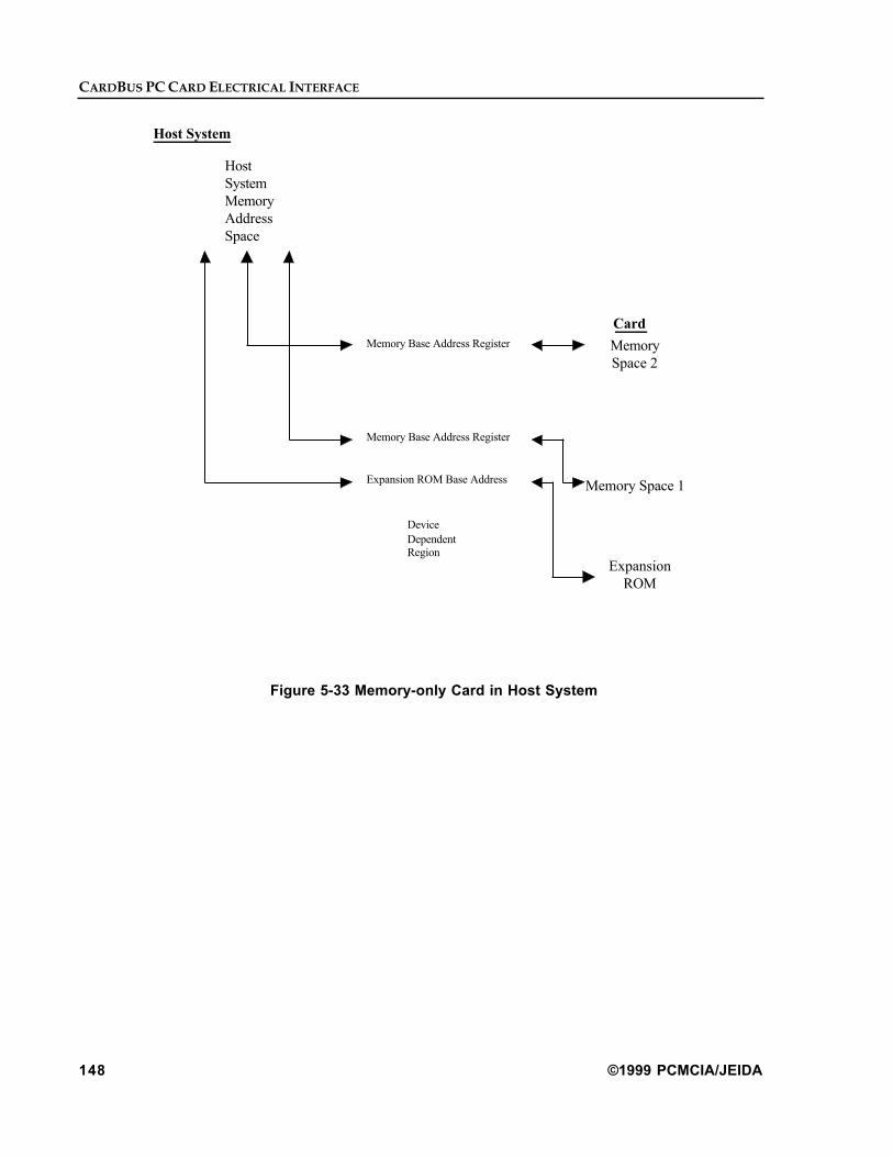
CARDBUS PC CARD ELECTRICAL INTERFACE
148 ©1999 PCMCIA/JEIDA
Device
DependentRegion
Host System
HostSystemMemoryAddressSpace
Memory Base Address Register
Memory Base Address Register
Expansion ROM Base Address
MemorySpace 2
Memory Space 1
ExpansionROM
Card
Figure 5-33 Memory-only Card in Host System

ELECTRICAL SPECIFICATION
© 1999 PCMCIA/JEIDA 149
A PC Card is not required to have any I/O spaces, and thus might contain only memory spaces, asin Figure 5-33. In this example, an expansion ROM is included, which is another optionalcomponent of a CardBus PC Card.
Device
DependentRegion
Host System
HostSystemMemoryAddressSpace
I/O Base Address Register
Memory Base Address Register
Memory Base Address Register
I/O Space 1
I/O Space 2
Card
HostSystemI/OAddressSpace
I/O Base Address Register
Figure 5-34 I/O Space-only Card in a Host System with a Separate I/O Space
Figure 5-34 depicts a card that has I/O spaces and no memory spaces in a system with a separatehost I/O space. Note that the card I/O space could be memory-mapped as in Figure 5-32.

CARDBUS PC CARD ELECTRICAL INTERFACE
150 ©1999 PCMCIA/JEIDA
Device
DependentRegion
Host System
HostSystemMemoryAddressSpace
Memory Base Address Register
I/O Base Address Register
Memory Base Address Register
Memory Base Address Register
Expansion ROM Base Address
MemorySpace 2
I/O Space
Memory Space 1
ExpansionROM
Card
HostSystemI/OAddressSpace
Figure 5-35 Card and Host with All Spaces Described
Figure 5-35 shows a card having all of the allowable card spaces, and using both host systemmemory space and a separate host I/O space.
The programming model for CardBus PC Card takes into consideration all of the above spaces, bothin describing what types of configuration information may reside where and in defining how cardand system software may gain access to a given space. Tuples may reside in any card space exceptI/O space and the first 64 bytes of configuration space. For complete information on tuple definitionsand tuple chain traversal, see the Metaformat Specification.
Each function on a CardBus PC Card has a set of four status registers associated with it. (See 5.2CardBus PC Card Operation.) These registers are located in that function's memory space at thelocation given by the CISTPL_CONFIG_CB tuple in that function's CIS. (See the MetaformatSpecification.)
5.4.2.1 Configuration Space
The CardBus PC Card configuration space is a 256 byte memory region which is accessed during aconfiguration access cycle. Configuration space is divided into two parts:

ELECTRICAL SPECIFICATION
© 1999 PCMCIA/JEIDA 151
• a mandatory 64 byte predefined header.
• a device-dependent region which is always physically present, but which might not beimplemented by the card and used by its software.
Cards have a separate configuration space for each implemented function.
The CardBus PC Card configuration space is as described in Figure 5-36. Following the figure eachelement is defined. "Reserved" indicates that the register is reserved for future use. "Allocated"indicates that the register is not defined for CardBus PC Card and must not be redefined as otherenvironments may use the register. The purpose of the "Allocated" registers is to maintaincompatibility between CardBus PC Card and other environments. CardBus PC Card systemsoftware must not make use of any of the information which may be stored in these "Allocated"fields.

CARDBUS PC CARD ELECTRICAL INTERFACE
152 ©1999 PCMCIA/JEIDA
All unimplemented registers must return all 0's when read. Registers which are marked "Allocated"may contain readable values. However, these values will be ignored by all CardBus PC Cardsoftware and no programmatic interface is provided with which to access them.
Allocated Allocated
Status Command
00h
Allocated Allocated 08h
BIST Latency Timer 0Ch
Base Address Register 10h
38h
04h
Header Type Cache Line Size
Base Address Register 14h
Base Address Register 18h
Base Address Register 1Ch
Base Address Register 20h
Base Address Register 24h
CIS Pointer 28h
Reserved 2Ch
Expansion ROM Base Address 30h
Reserved 34h
Reserved
3Ch
Beginning of Device Dependent Space 40h
Tuple Space
Tuple Space
AllocatedInterrupt PinAllocatedAllocated
44h
End of Device Dependent Space FFh
Pre-Defined Header64 bytes
Device Dependent Space192 bytes
31 16 15 0
Cap_Ptr
Figure 5-36 CardBus PC Card Configuration Space
CardBus PC Card header fields and registers are defined in the following sections. (See also5.4.2.1.13 Register Summary.)

ELECTRICAL SPECIFICATION
© 1999 PCMCIA/JEIDA 153
5.4.2.1.1 Command
This register specifies a function's ability to generate and respond to the different access cyclespossible for CardBus PC Card. When this register has a value of 0, the function accepts onlyconfiguration accesses. Configuration accesses are required to be supported by all functions on allcards as a minimum level of functionality.
Individual fields in the Command register may or may not be implemented depending on afunction's use. For instance, functions for which no I/O accesses are possible should not implement awritable field at location 0. After a card is mapped into the host system, system software will enablethe appropriate accesses (memory and/or I/O) by setting the memory and/or I/O bits in theCommand register. After the CRST# signal is asserted, all fields in the Command register are reset(given a value of 0). Additionally, after the card reset is complete, the Fast Back-to-Back Enable fieldwill contain an appropriate value based on the capabilities of the system. At this time (after the cardis reset) the client and/or the system software may reconfigure the card as necessary. Figure 5-37shows the layout of the register and Table 5Ð17 explains the meanings of the different fields in theCommand register.
01234567891015
Reserved
Fast Back-to-Back Enable
SERR# Enable
Wait Cycle Control
Parity Error Response
VGA Palette Snoop
Memory Write and Invalidate Enable
Special Cycles
Bus Master
Memory Space
I/O Space
Figure 5-37 COMMAND Register Layout

CARDBUS PC CARD ELECTRICAL INTERFACE
154 ©1999 PCMCIA/JEIDA
Table 5Ð17 COMMAND Register Field Definitions
Bit Field Name Description
0 I/O Space Specifies whether a function responds to I/O space accesses. If reset, the functiondoes not respond to I/O space accesses. If set, the function responds to I/O spaceaccesses. If the Memory Space field is reset and this field is reset, then the card isaccepting only configuration accesses.
1 Memory Space Specifies whether a function responds to memory space accesses. If reset, thefunction does not respond to memory space accesses. If set, the function responds tomemory space accesses. If the I/O Space field is reset and this field is reset, then thecard is accepting only configuration accesses.
2 Bus Master Specifies whether a function can act as a master on the bus. If reset, the function maynot generate bus accesses. If set, the function may behave as a bus master.
3 Special Cycles Specifies whether a function responds to Special Cycle operations. If reset, thefunction ignores all Special Cycle operations. If set, the function may monitor SpecialCycle operations.
4 Memory Write andInvalidate Enable
Specifies whether this master may generate the Memory Write and Invalidatecommand. If reset, Memory Write must be used. If set, masters may generate thecommand. This field must be implemented by masters that can generate the MemoryWrite and Invalidate command.
5 VGA Palette Snoop Specifies how palette registers are handled by VGA compatibles. If reset, the functionshould treat palette accesses like all other accesses. If set, special palette snoopingbehavior is enabled (i.e. the function must not respond). VGA compatibles mustimplement this field.
6 Parity Error Response Specifies how the function responds to parity errors. If reset, the function must ignoreany parity error that it detects and continue normal operation. If set, when a parityerror is detected, the function must take whatever action is defined for it in that event.All functions must implement this bit field. Functions must generate parity even if theirparity checking mechanism is disabled.
7 Wait Cycle Control This controls whether or not a card does address/data stepping. If reset, the card doesnot do stepping. If set, the card does stepping. If a card always does stepping, or neverdoes it, then this field may be read-only. For cards that can do either, however, thefield must be read/write and must be initialized to 1 after the card is reset. This fieldhas the same value for all of the functions on a card.
8 SERR# Enable This controls whether or not the SERR# output buffer is enabled. If reset, the SERR#output buffer is disabled. If set, the SERR# output buffer is enabled. All functions mustimplement this field. This field and the Parity Error Response field at location 6 mustboth be set in order for address parity errors to be reported.
9 Fast Back-to-BackEnable
This controls whether or not a master can do fast back-to-back transactions todifferent devices. This will be set by system software if the adapter and the card arefast back-to-back capable. If reset, fast back-to-back transactions are only allowed tothe same agent. If set, the master is allowed to generate fast back-to-backtransactions to different agents.
10-15 Reserved.
5.4.2.1.2 Status
This register holds run-time status information for bus related events. (See Figure 5-38: STATUSRegister Layout and Table 5Ð18 STATUS Register Field Definition.) Functions implement fieldsbased on the presence of functionality, and should not implement fields they will not use. Forinstance, a function which acts as a target but will never signal target-abort, should not implementthe Signaled Target Abort field at location 11.
This register can be read without side-effects. Writes are slightly different in that fields can be reset,but not set. A field is reset whenever the register is written and the data in the correspondinglocation is a 1. For instance, to clear the field at location 14 and not affect any other fields, write thevalue 0100000000000000B to the register. After a card reset all implemented fields in this register arereset, except for the DEVSEL# Timing and Fast Back-to-Back Capable bit fields which are read-only.

ELECTRICAL SPECIFICATION
© 1999 PCMCIA/JEIDA 155
06715
Reserved
Extended Capabilites Support
Fast Back-to-Back Capable
Data Parity Dectecte
CDEVSEL# Timing
Signaled Target Abort
Received Target Abort
Received Master Abort
Received System Error
Detected Parity Error
14 13 12 11 10 9 8
00 - fast01 - medium10 - slow
5 4
Figure 5-38: STATUS Register Layout
Table 5Ð18 STATUS Register Field Definition
Bit Field Name Description
0-3 Reserved
4 Extended CapabilitesSupport
If set, indicates this device supports the PCI Extended Capabilities feature and theCapabilities Pointer at offset 34h should be used to locate the offset to the first datastructure. See the PCI Bus Power Management Specification for CardBusCards section for further definition of extended capability.
5-6 Reserved
7 Fast Back-to-BackCapable
This read-only field indicates whether or not the target is capable of accepting fastback-to-back transactions when the transactions are not to the same agent. If reset,the function cannot accept these transactions. If set, the function can accept thesetransactions.
8 Data Parity Detected This field is only implemented by bus masters. If set, then three conditions must havebeen met: (1) the bus agent asserted CPERR# itself or observed CPERR# asserted;(2) the agent setting the bit field acted as the bus master for the operation in which theerror occurred; (3) the Parity Error Response bit field (Command Register) is set.
9-10 CDEVSEL# Timing This field encodes the timing of CDEVSEL#. The three allowable timings are encodedas 00b for fast, 01b for medium, and 10b for slow (11b is reserved). This field is read-only and must indicate the slowest time in which a card asserts CDEVSEL# for anybus command except Configuration Read and Configuration Write.
11 Signaled Target Abort This field must be set by a target whenever it terminates a transaction with target-abort. Functions that will never signal target-abort do not need to implement this field.
12 Received Target Abort This field must be set by a master whenever its transaction is terminated with target-abort. All masters must implement this field.
13 Received Master Abort This field must be set by a master whenever its transaction, except for SpecialCycles, is terminated with master-abort. All masters must implement this field.
14 Signaled System Error This field must be set whenever the function asserts CSERR#.
15 Detected Parity Error This field must be set by the function whenever it detects a parity error, even if parityerror handling is disabled.

CARDBUS PC CARD ELECTRICAL INTERFACE
156 ©1999 PCMCIA/JEIDA
5.4.2.1.3 Cache Line size
This register specifies the system cache line size in units of 32-bit words. This register must beimplemented by masters that can generate the Memory Write and Invalidate command. Functionsparticipating in the caching protocol use this register to know how to disconnect burst accesses atcache line boundaries. The default value of this register when the card is reset, is 0. This register isset by Card Services to inform the card what size is supported by the system. A size of 0 generallyindicates that the memory spaces of this function is not cacheable, i.e. software must guaranteecoherency if it is cached. Since this register indicates the level of system support, all cacheablefunctions on a card will have the same value for Cache Line Size, which is defined by the system.
5.4.2.1.4 Latency Timer
This register specifies, in units of bus clocks, the value of the Latency Timer for this bus master. Thisregister must be implemented as writable by any master that can burst more than two data phases.This register may be implemented as read-only for cards that burst two or fewer data phases, butthe hardwired value must be limited to 16 or less. A typical implementation would be to build thefive high-order bits (leaving the bottom three as read-only), resulting in a timer granularity of eightclocks. The default value of the non-read-only fields of this register when the card is reset is 0.
5.4.2.1.5 Header Type
This register identifies the layout of bytes 10H through 3FH in configuration space and also whetheror not the card contains multiple functions. Bit 7 in this register is used to identify a multi-functioncard. If reset, then the card has a single function. If set, Bit 7 indicates that the card has multiplefunctions. Bits 6 through 0 specify the layout of bytes 10H through 3FH. One encoding, 00H, isdefined and specifies the layout of the pre-defined header space shown in Figure 5-36. This headerlayout allows compatible information to be stored for both CardBus PC Card configuration spacesand those used by other environments. The remaining encodings (1-127) are reserved for futureuse.
Each function on the card has a configuration space including the pre-defined header. Every cardmust contain function 0.
5.4.2.1.6 Built-in Self Test (BIST)
This optional register is used for control and status of BIST. Functions that do not support BIST mustalways return a value of 0 (i.e., treat it as a reserved register). A function whose BIST is invokedshould not prevent normal operation of the bus. Figure 5-39 shows the layout for the BIST register.Table 5Ð19 defines the BIST register fields.
067
Reserved
Start BIST
BIST Capable
Completion Code
5 4 3
Figure 5-39 BIST Register

ELECTRICAL SPECIFICATION
© 1999 PCMCIA/JEIDA 157
Table 5Ð19 BIST Register Fields
Bit Field Name Description
7 BIST Capable If reset, function is not BIST capable. If set, function supports BIST.
6 Start BIST If reset, BIST is complete. If set, invoke BIST. Test fails if BIST is not complete after 2seconds.
5-4 Reserved. Only reset is supported.
3-0 Completion Code A value of 0 means the function has passed its test. Non-zero values mean the testfailed. Function-specific failure codes can be encoded in the non-zero value.
5.4.2.1.7 Base Address Register
These registers provide the beginning Host System address for mapping CardBus PC Card memoryand I/O spaces into the Host System. Such mappings use Base Address Register windows. Thereare a maximum of six Base Address Registers per configuration space. A Base Address Registermay refer to either a memory or an I/O mapping. Since it is not required that all CardBus PC Cardhost systems implement a separate I/O space, any I/O space on a CardBus PC Card must be able tobe mapped into the host system memory address space, i.e., memory-mapped I/O.
A Base Address Register that contains a zero value, in bits (31:4), is in a disabled state. No accessshall be accepted by a card for a Base Address Register with bits (31:4) set to zero. All base addressregisters must be have bits (31:4) set to zero by assertion of CRST#.
CardBus PC Card does not require that any Base Address Registers be implemented in a CardBusPC Card function. However, the only way to access memory or I/O space on a CardBus PC Cardfrom a host system is via the Base Address Registers. The layout for a Base Address Registerreferring to a memory mapping is given in Figure 5-40.
0
Base Address
Prefetchable
Type
Memory Space Indicator
0
123431
Figure 5-40 Base Address Register Mapping for Memory Space
The Prefetchable field is set by the card if the following are all true:
• There are no side effects on reads.
• The function returns all bytes on reads regardless of the byte enables.
• Host bridges can merge processor writes into this range without causing errors.
The field must be reset otherwise. Any function that has memory which behaves like normalmemory, but will not be participating in CardBus PC Card's caching protocol, should mark therange as prefetchable. A linear frame buffer in a graphics device is an example of a range whichshould be marked prefetchable.
The Type field indicates valid placements in memory space for the mapping. The values aredefined as below in Table 5Ð20.

CARDBUS PC CARD ELECTRICAL INTERFACE
158 ©1999 PCMCIA/JEIDA
Table 5Ð20 Meaning of the Type Fields for a Memory Base Address Register
Bits 2/1 Meaning
00 Base Address Register is 32 bits wide and mapping can be done anywhere in the 32-bit memory space.
01 Base Address Register is 32 bits wide but must be mapped below 1M (Real Mode mapping) in memoryspace.
10 Allocated.
11 Reserved
Bits 0-3 of a memory Base Address Register are read only. This results in 16 byte alignment forCardBus PC Card base memory addresses. The number of upper bits that a function's configurationspace actually implements in this Base Address Register depends on how much of the address spaceto which the memory associated with that Base Address Register will respond. In other words, thenumber of upper bits implemented indicates directly the size of the mapping required and leads toa power-of-2 sizing and alignment for the mapping.
The layout for a Base Address Register referring to an I/O mapping is given in Figure 5-41.
0
Base Address
Reserved
I/O Space Indicator
1
1231
0
Figure 5-41 Base Address Register Mapping for I/O Space
Bits 0-1 of an I/O Base Address Register are read only. This results in 4 byte alignment for CardBusPC Card I/O addresses. The function may in fact decode all 32 bits of a presented address, whichallows a one (1) byte granularity to be supported without waiting the extra cycle for a byte enable.(See also 5.2.2.2 Addressing.) The number of upper bits that a function's configuration space actuallyimplements in this Base Address Register depends on how much of the I/O space to which thisfunction will respond. In other words, the number of upper bits implemented indicates directly thesize of the mapping required and leads to a power-of-2 sizing and alignment for the mapping.
All CardBus PC Cards implementing I/O spaces must to be able to be memory-mapped as well asmapped via I/O Base Address Registers. Therefore, for those cards implementing an I/O spacethere will be, as well as any I/O Base Address Registers mapping that space(s), at least 1 memoryBase Address Register to also map the space. The memory Base Address Register associated withthe I/O space(s) immediately follows the I/O space(s)'s I/O Base Address Register(s) inconfiguration space.
There are six DWORD locations allocated for Base Address Registers, with the first starting at offset10H.
5.4.2.1.8 CIS Pointer
This read-only register points to where the CIS begins, in one of the following spaces:
• configuration space Ñ must begin in device-dependent space at or after location 40H.
• memory space Ñ may be in any of the memory spaces.
• Expansion ROM space Ñ may be in any of the images.

ELECTRICAL SPECIFICATION
© 1999 PCMCIA/JEIDA 159
Each configuration space of a multi-function card must have its own CIS, pointed to by the CISPointer in its configuration space. The encoding for this pointer is given below in Figure 5-42.
0
Address Space Offset
ROM Image Address Space Indicator
1232731 28
Figure 5-42 CIS POINTER Layout
The Address Space Indicator field indicates in which of this function's address spaces the CIS begins.The encoding for this field is given below in Table 5Ð21.
Table 5Ð21 Address Space Indicator Values
Value Meaning
0 CIS begins in device-dependent configuration space.
1-6 The CIS begins in the memory address space governed by one of the six Base Address Registers. For example,if the value is 2, then the CIS begins in the memory address space governed by Base Address Register 2.
7 The CIS begins in the Expansion ROM space.
The value of the Address Space Offset gives the offset, into the address space indicated by theAddress Space Indicator field, at which the CIS begins. (See Table 5Ð22 Address Space OffsetValues.)
Table 5Ð22 Address Space Offset Values
Address Space Indicator Space Type Address Space Offset Values
0 configuration space 40H ≤ value ≤ F8H. The address in device-dependentconfiguration space at which the CIS starts.
x; 1 ≤ x ≤ 6 memory space 0 ≤ value ≤ FFFF FFF8H. This is the offset into the memoryaddress space governed by Base Address Register x.Adding this value to the value in the Base Address Registergives the location of the start of the CIS.
7 expansion ROM 0 ≤ image ≤ FH, 0 ≤ value ≤ 0FFF FFF8H. This is the offsetinto the expansion ROM address space governed by theExpansion ROM Base Register. The image number is inthe uppermost nibble of the Address Space Offset. Thevalue consists of the remaining bytes.
The image is the image number used as the locationreference for the start of the CIS. The value is the offset ofthe start of the CIS from the base of that image. Adding thisoffset plus the starting offset of the image to the value in theExpansion ROM Base Register gives the location of thestart of the CIS.
Note that the above definition ensures that no properly implemented CIS Pointer register will everhave the value 0. It is required that each function in a multi-function CardBus PC Card have thisregister implemented and that the pointer indicates the location of a valid CIS. (See 5.5.3.2 RequiredCIS.)

CARDBUS PC CARD ELECTRICAL INTERFACE
160 ©1999 PCMCIA/JEIDA
5.4.2.1.9 Expansion ROM Base Address Register
The 4-byte register at offset 30H in configuration space is defined to handle the base address andsize information for an expansion ROM. Figure 5-43 shows how this register is organized. Theregister functions exactly like a 32-bit Base Address Register except that the encoding and usage ofthe lower bits is different. The number of bits, out of the upper 21 bits, that a function'sconfiguration space actually implements depends on what address alignment the function supports.Functions that support an expansion ROM must implement this register.
0
Expansion ROM Base Address Reserved
Address Decode Enable
11031 11
Figure 5-43 Expansion ROM Base Address Register Layout
The field at location 0 in the register is used to control whether or not the function accepts accesses toits expansion ROM. When set, this field indicates that address decoding is enabled using theparameters in the other part of the register. This allows a function to be used with or without anexpansion ROM depending on system configuration. When reset, the function's expansion ROMaddress space is disabled. The Memory Space field in the Command register has precedence overthe Expansion ROM Enable field. A function will only respond to accesses to its expansion ROM ifboth the Memory Space field and the Expansion ROM Base Address Enable field are set.
Since the Expansion ROM Base Address Register controls all accesses to the Expansion ROM, aCardBus PC Card device must also respond to a write access to the Expansion ROM, even if theExpansion ROM is a read-only device. A CardBus PC Card device responds to such write accesses asif it was a successful transaction (CDEVSEL# and CTRDY# asserted, with CSTOP# negated). Thewrite data should be ignored and should not affect the operation of the CardBus PC Carddevice.(See also 5.4.2.4 Expansion ROM.)
An Expansion ROM Base Address Register that contains a zero value, in bits (31:11), is in a disabledstate. No access shall be accepted by a card for the Expansion ROM Base Address Register with bits(31:4) set to zero. The Expansion ROM Base Address Registers must be have bits (31:11) set to zeroby assertion of CRST#.
5.4.2.1.10 Cap_Ptr
The 8-bit Capabilities Pointer at location 34h is used to point to the beginning of the first PCIdefined Extended Capabilities data structure. It represents an offset from the beginning of the PCIConfiguration Space into the Configuration Space where the first data structure will be found.
If the PCI Extended Capabilities feature is not implemented, this value is 0.
See the PCI Bus Power Management Specification for CardBus Cards section for further definitionof extended capability.
5.4.2.1.11 Interrupt Pin
The Interrupt Pin register tells whether or not the function uses the interrupt pin. Functions whichdo use the interrupt pin must set this register. Functions which don't use the interrupt pin mustreset this register. This register is read-only. Note that when multiple functions exist on a CardBus

ELECTRICAL SPECIFICATION
© 1999 PCMCIA/JEIDA 161
PC Card and more than one uses the interrupt pin and these functions are concurrently enabled, thefunctions share the interrupt pin.
5.4.2.1.12 Tuple Space
The device-dependent configuration space of a CardBus PC Card may contain a tuple chain. Thistuple chain may start anywhere on or after 40H in configuration space and must be contiguous untila CISTPL_END is reached. This tuple chain may contain a LongLink tuple to another tuple chain inanother space associated with that function. Tuple space must begin with a CISTPL_LINKTARGETtuple. (See the Metaformat Specification.)
5.4.2.1.13 Register Summary
All of the registers defined above may be accessed by CardBus PC Card system software.Additionally, for some of the registers, the CardBus PC Card system software will provide the clientwith an access API. (See the Card Services Specification.) Table 5Ð23 below gives a summary of theusage characteristics of the configuration space registers. The columns in Table 5Ð23 have thefollowing meanings:
Register the name of the register in CardBus PC Card configuration space.
Field if applicable, the separately accessible field in the register.
Mandatory YES - the register or field is required.
NO - the register or field is optional, based on the function.
Function Unique YES - within a multi-function card, each function could give this register or field a different value.
NO - it is required that this register or field be given the same value by all functions on the card. Infact, it would be possible to alias all of the occurrences of this register or field in all of the functions tothe same physical register.
Interface Control YES - this register or field either gives information about or controls the card to system interface.
NO - this register or field does not give information about or control the card to system interface.
System Software(Read/Write)
YES - CardBus PC Card system software is expected to read from or write to this register or field.
NO - CardBus PC Card system software is not expected to read from or write to this register orfield.
Client Software(Read/Write)
YES - the function's client software is allowed to read from or write to this register or field. (See theCard Services Specification.)
NO - the function's client software does not access this register or field. The knowledge provided bythis register or field may be available to the client via the Card Services interface. However, theclient does not directly read from this register or field.

CARDBUS PC CARD ELECTRICAL INTERFACE
162 ©1999 PCMCIA/JEIDA
Table 5Ð23 Configuration Space Register Usage Summary
Register Mandatory Function Interface System Software Client Software
Field Unique Control Read Write Read Write
Command YES
I/O Space YES YES YES YES YES NO NO
Memory Space YES YES YES YES YES NO NO
Bus Master YES YES YES YES YES YES YES
Special Cycles YES YES YES YES YES NO NO
Memory Write andInvalidate Enable
YES YES YES YES YES YES YES
VGA Palette Snoop NO YES YES YES YES YES YES
Parity Error Response YES YES YES YES YES NO NO
Wait Cycle Control YES NO YES YES YES NO NO
SERR# Enable YES YES YES YES YES NO NO
Fast Back-to-BackEnable
YES NO YES YES YES NO NO
Status YES
Extended CapabilitySupport
NO YES NO YES NO YES NO
Fast Back-to-BackEnable
YES NO YES YES YES NO NO
Data Parity Detected NO YES YES YES YES NO NO
DEVSEL# Timing YES NO YES YES NO NO NO
Signaled Target Abort NO YES YES YES YES NO NO
Received Target Abort NO YES YES YES YES NO NO
Received Master Abort NO YES YES YES YES NO NO
Signaled System Error NO YES YES YES YES NO NO
Detected Parity Error YES YES YES YES YES NO NO
Cache Line Size YES NO YES YES YES NO NO
Latency Timer YES NO YES YES YES NO NO
Header Type YES NO NO YES NO NO NO
BIST NO YES NO NO NO YES YES
Base Address Register NO YES YES YES YES YES NO
Expansion ROM BaseRegister
NO YES YES YES YES YES NO
Interrupt Pin YES YES YES YES NO NO NO
CIS Pointer YES YES NO YES NO YES NO
5.4.2.2 Memory Space
While there is no Attribute Memory, as defined for 16-bit PC Cards, on CardBus PC Cards, CardBusPC Cards' memory space(es) could be viewed as 16-bit PC Card-like Common Memory. EachCardBus PC Card memory device is mapped into host system address space via one of the six BaseAddress Registers in configuration space.
Because CardBus PC Card sockets support 16-bit PC Cards, the CardBus PC Card programmingmodel must support 16-bit PC Card memory mapping mechanisms as well as the Base AddressRegister mappings used for CardBus PC Cards. This includes the 16-bit PC Card window mapping

ELECTRICAL SPECIFICATION
© 1999 PCMCIA/JEIDA 163
where a window of a given size is requested between a card offset address and a host system baseaddress.
Whether the memory space is mapped into host system address space via a 16-bit PC Card-likemapping from a 16-bit PC Card or a Base Address Register mapping from a CardBus PC Card, it isimportant that the card software manage the mapping. (See the Card Services Specification.)
Tuple chains may appear anywhere in memory space. Any tuple chains in memory space, unlikethose in configuration space, may be mapped directly into the host system address space andaccessed by the client, although the Card Services tuple parsing routines are still the preferredaccess mechanism partly because those tuple chains in CardBus PC Card configuration space cannotbe directly mapped into the host system address space.
5.4.2.3 I/O Space
When used in CardBus PC Card systems which implement a separate host system I/O space, cardsare assigned I/O addresses. (See the Card Services Specification.)
5.4.2.4 Expansion ROM
An expansion ROM may be mapped into the host system address space via the Expansion ROMBase Address Register in the configuration space. The ROM consists of one or more images, each ofwhich may apply to different system and processor architectures. Each image must start on a 512-byte boundary and must contain the CardBus PC Card expansion ROM header. The starting pointof each image within the expansion ROM depends on the size of previous images. The last image ina ROM has a special encoding in the header to identify it as the last image.
If an expansion ROM is present, as indicated by the Expansion ROM Base Address Register, thenthere may be tuple chains in any of the images.
At the beginning of each expansion ROM image is an expansion ROM header, as described inTable 5Ð24, below. All of the registers in the expansion ROM Image Header and in the CardBus PCCard Data Structure, unless otherwise stated, are required to be present, with legal values.
Table 5Ð24 Expansion ROM Image Header
Offset Length Value Description
0H 1 55H ROM Signature, byte 1
1H 1 AAH ROM Signature, byte 2
2H-17H 16 variable Reserved (processor architecture uniquedata)
18H-19H 2 variable Pointer to CardBus PC Card Data Structure(defined in Table 5Ð25). This pointer musthave a value of at least 20H, in order not toconflict with the placement of the imageheader.
ROM Signature - this is a two-byte field containing 55H in the first byte and AAH in the secondbyte. This signature must be the first two bytes of the ROM address space for each image of theROM.
Pointer to CardBus PC Card Data Structure - this is a two-byte pointer in little endian format whichpoints to the CardBus PC Card Data Structure. The reference point for this pointer is the beginningof the ROM image.

CARDBUS PC CARD ELECTRICAL INTERFACE
164 ©1999 PCMCIA/JEIDA
The CardBus PC Card Data Structure must be located within the first 64 KBytes of the ROM imageand must be DWORD aligned. The CardBus PC Card Data Structure contains the informationsummarized in Table 5Ð25. Details of each field are given after the figure. "Reserved" in thediagram below indicates that the register is reserved for future use. "Allocated" indicates that theregister is not defined for CardBus PC Card and must not be redefined as other environments mayuse the register. The purpose of the "Allocated" registers is to maintain compatibility betweenCardBus PC Card and other environments. CardBus PC Card system software will not make use ofany of the information which may be stored in these fields.
Table 5Ð25 CardBus PC Card Data Structure Fields
Offset Length Description
0H 4 Signature, the string "PCIR"
4H 4 Allocated
8H 2 Pointer to Vital Product Data
AH 2 CardBus PC Card Data Structure Length
CH 1 CardBus PC Card Data Structure Revision
DH 3 Allocated
10H 2 Image Length
12H 2 Revision Level of Code/Data
14H 1 Code Type
15H 1 Indicator
16H 2 Reserved
Signature - these four bytes provide a unique signature for the CardBus PC Card Data Structure.The string "PCIR" is the signature with "P" being at offset 0, "C" at offset 1, etc.
Pointer to Vital Product Data - the Pointer to Vital Product Data (VPD) is a 16-bit field which is theoffset from the start of the ROM image and points to the VPD. This field is in little-endian format.The VPD must be within the first 64 KBytes of the ROM image. A value of 0 indicates that no VPDis in the ROM image. The content of the VPD structure is not currently defined.
CardBus PC Card Data Structure Length - this is a 16-bit field which defines the length of the datastructure from the start of the data structure (the first byte of the Signature field). This field is inlittle-endian format and is in units of bytes.
CardBus PC Card Data Structure Revision - this is an 8-bit field which identifies the data structurerevision level. This revision level is 0.
Image Length - this is a two-byte field which represents the length of the image. This field is inlittle-endian format and gives the value in units of 512 bytes.
Revision Level - this is a two-byte field which contains the revision level of the code in the ROMimage.
Code Type - this is a 1-byte field which identifies the type of code contained in this section of theROM. The code may be executable binary for a specific processor and system architecture orinterpretive code. Table 5Ð26 describes the available Code Types.

ELECTRICAL SPECIFICATION
© 1999 PCMCIA/JEIDA 165
Table 5Ð26 Code Type Descriptions
Type Description
0 Intel Architecture, PC-AT compatible
1 Open Firmware Standard23
2-FFH Reserved
Indicator - bit 7 in this field tells whether or not this is the last image in the ROM. If reset, anotherimage follows. If set, this is the last image. Bits 0-6 are reserved.
5.5 Requirements For CardBus PC Cards and Sockets
5.5.1 OverviewThis chapter describes the minimum hardware and software interfaces that PC Card and systemdesigners can rely on for basic compatibility across PC Cards, systems, and related software. Theseinterfaces ensure that the CardBus PC Card can meet the PCMCIA/JEIDA goal of PC Cardinteroperability.
5.5.2 Software RequirementsCardBus PC Card allows PC Cards and sockets to be accessed by multiple PC Card-aware devicedrivers, configuration utilities, and applications with efficient and non-conflicting use of systemresources. The primary components of the software interface are Socket Services and Card Services.Socket Services provides the lowest-level function set for socket hardware adapter control. CardServices allocates resources and coordinates PC Card-related activities for higher-level clients. Bothcomponents can be developed as a single module as long as all functions described are available.
5.5.2.1 Socket Services
Socket Services functionality must be provided. It is the lowest level software layer, providing onlysocket-control functions and low-level PC Card functions accessible through control of CardBus PCCard sockets. The services provide hardware-independent control functions that are used tomanipulate implementation-dependent hardware. This isolates higher-level software from mosthardware implementation dependencies allowing different socket implementations to be supportedby a common client. Socket Services is the only interface defined and supported by the PC CardStandard.
Once Card Services is loaded, Card Services has exclusive use of Socket Services. After CardServices is initialized, any software using Socket Services will receive an error status when accessingSocket Services functions directly. This allows the CardBus PC Card-compatible software to operatewithout conflicts and gain control of host system resources. (See also the Socket ServicesSpecification.)
23 Open Firmware is a processor architecture and system architecture independent standard for dealing with device
specific option ROM code. Documentation for Open Firmware is available in the IEEE P1275-1994 Standard forBoot (Initialization, Configuration) Firmware Core Requirements and Practices.

CARDBUS PC CARD ELECTRICAL INTERFACE
166 ©1999 PCMCIA/JEIDA
5.5.2.2 Card Services
Card Services is the only required software interface for managing CardBus PC Cards in CardBusPC Card-compliant systems. It provides the capability of client registration for card event call backsand meets the minimal requirements for manipulating CardBus PC Card-compliant host systeminterfaces. The Card ServicesÕ specification explicitly defines a guaranteed minimum set of cardcontrol functions on which higher-level software and associated PC Cards can rely. Most of the CardServices functions are used by clients only for installation and configuration.
It is important to recognize that more than one type of adapter can be present in any given system.One adapter could be part of the motherboard and another adapter could be plugged into a systemexpansion slot. In this case, there will typically be several implementations of Socket Services, oneimplementation to control each adapter type. However, even if there is more than one SocketServices handler, there can be only one Card Services implementation present in a system. CardServices is the central coordinator for clients to acquire system and socket resources (e.g., mappingwindows, system mappable address space, etc.). The hardware notification of PC Card insertion andstatus change events from all adapters goes to a single Card Services handler. (See also the CardServices Specification.)
5.5.2.3 System Resource Availability
Multiple CardBus PC Card-aware device drivers, utilities, and applications share system resourcesin providing for PC Card access. Therefore, CardBus PC Card compliance cannot guarantee that anygiven client of Card Services will always be granted a requested resource. If Card Services is unableto provide resources to a client due to resource availability limitations, it returns a failure indication.In this case, the client can try to operate with different or fewer resources or may simply report thatit is unable to provide its function.
5.5.2.4 System Resource Determination
Each implementation of Card Services must have some implementation-dependent way todetermine the system hardware resources (e.g., memory address space, I/O address space,interrupts) present in a given system. Card Services must know what system I/O and memoryaddress space is usable by the adapter hardware, what system I/O and memory address space isunused, what interrupts can be steered by the adapter hardware, and what interrupts are unused.
Note that automated processes to determine system resource availability are usually not 100%accurate. Also the system configuration could change rendering a pre-initialized table obsolete. As aresult, there must be the ability for later adjustment of the Card Services resource table.
Therefore, CardBus PC Card-compliant systems must provide the following:
an automated method of initializing CardServices with the available resources (those not
preassigned)
or a Card Services that is preinitialized with theavailable resources
and
a method of later modifying the Card Services set of available resources based on the changing configuration ofnon-PC Card components in the host system.24
24This method does not have to be supported if an automated process can guarantee 100% accuracy in dynamically
determining system resource availability and it is used to initialize Card Services whenever resources change.

ELECTRICAL SPECIFICATION
© 1999 PCMCIA/JEIDA 167
5.5.2.5 Enabler Support
The purpose of an enabler is to allow a single piece of software to configure and unconfigure a PCCard to prevent the redundancy of every PC Card requiring separate and unique configurationsoftware.
Enablers recognize PC Cards in one of two ways. First, they may recognize a card specifically frominformation in the Card Information Structure (CIS) that is unique to that card. For example, someenablers use combinations of the manufacturer string and product string from the VERS_1 tuple andthe Manufactuer ID and Function ID tuples. Second, enablers may recognize a PC Card solely fromits Function ID tuple. For most Data/FAX modems, a Function ID that indicates the PC Card has aserial interface causes the card to be configured as the next available COM port.
Once a card is configured, it may be used by software that is or is not aware that the functionality islocated on a PC Card. If the software is PC Card-aware, it may piggy-back on the efforts of theenabler and use the card's functionality until the card is removed and the enabler releases thesystem resources used by the card.
If the software is not PC Card-aware, it must locate the card's resources where the enabler mappedthem into the host system's address space. For most cards this means assuming the PC Card isplaced at the same locations typically used by standard ISA peripherals that perform the samefunctions.
Some cards offer functionality that use configuration files to describe where they are located insystem memory address space. As an example, network adapters have a NET.CFG orPROTOCOL.INI file describing the IRQ level, I/O address range and memory range used toaddress the adapter. In this case, the enabler must place the PC Card's resources as indicated in theconfiguration file.
It is recommended that CardBus PC Card software implementations provide for the support ofenablers. (See also Guidelines.)
5.5.3 Card RequirementsIn order for a socket to reliably recognize a PC Card and configure it, all CardBus PC Cards mustmeet certain minimum functionality requirements. This section outlines this minimum functionalityfor CardBus PC Cards.
5.5.3.1 Configuration Space
All CardBus PC Cards are required to implement configuration space for each function (see theCardBus PC Card Programming Model section of this specification). All other spaces, memory, I/O,and expansion ROM, are optional.
Common silicon (CardBus PC Card interface components designed for use on both PC cards andPCI) must implement configuration space as outlined in the "CardBus PC Card/PCI Common SiliconRequirements" guideline. This document specifies how to construct configuration space such that it isusable both by CardBus PC Card and PCI in addition to documenting electrical and protocolconsiderations.
5.5.3.2 Required CIS
CardBus PC Cards must implement a minimum set of tuples per function. (See the MetaformatSpecification.)

CARDBUS PC CARD ELECTRICAL INTERFACE
168 ©1999 PCMCIA/JEIDA
5.5.3.3 Required Signals
All CardBus PC Cards must implement the following signals:
Address and Data: CAD[31::0]CCBE[3::0]#CPAR
Interface Control: CFRAME#CTRDY#CIRDY#CSTOP#CDEVSEL#
Error Reporting: CPERR#CSERR#
System: CCLKCRST#
Card and Voltage Detect: CCD[2::1]#CVS[2::1]
Power and Ground: GND (four pins)VCC (two pins)
CardBus PC Cards with bus master capability must also implement:
Arbitration: CREQ#CGNT#CCLKRUN#
The following signals are optional:
CINT# for CardBus PC Cards requiring interrupt services
CSTSCHG for CardBus PC Cards which generate status changed events or remote wakeup
CBLOCK# for CardBus PC Cards containing shared memory (See 5.2.6.5 Supporting CBLOCK# and Write-back Cache Coherency.)
CAUDIO for CardBus PC Cards using the system's speaker
VPP1, VPP2 for CardBus PC Cards requiring this additional supply
The remote wakeup capability is optional even for CardBus PC Cards which implement theCSTSCHG pin. All connector pins associated with signals which aren't implemented must be no-connects on the PC Card.
5.5.3.4 Pull-up/Pull-down Resistors
When a PC Card is removed from the socket, there will be periods when the connector contactsbounce causing signals on the interface to glitch. During these times, the interface signals will float,possibly leading to false initiation or detection of cycles by the CardBus PC Card.
Therefore, CGNT# (for bus masters) and CFRAME# (on all cards) must be pulled-up to VCC on theCardBus PC Card using the resistor values specified in 5.3.3.3.1 Pull-up Values for Control Signals.The CGNT# resistor ensures the CardBus PC Card never initiates a cycle. The CFRAME# resistorensures that it never falsely detects a cycle.
5.5.3.5 CSTSCHG Support
CSTSCHG can be generated from a number of different sources, e.g., WP, BVD[2::1], READY, orremote wakeup. CardBus PC Cards do not have to implement all of the fields in the associated

ELECTRICAL SPECIFICATION
© 1999 PCMCIA/JEIDA 169
registers, just those which apply to the particular function. For example, LAN functions typicallywon't implement the write-protect switch but memory cards would.
There are additional requirements on CSTSCHG support when implementing PCI Bus PowerManagement for CardBus. Refer to the PCI Bus Power Management for CardBus Cards section forCardBus card specifics and the PC Card Host System Specification for additional details.
5.5.3.6 Power Consumption
The maximum power allowed for any CardBus PC Card is a function of the maximum current thatcan be supplied by the VCC pins.
It is anticipated that some systems either cannot or will not provide the full power budget. For thisreason, CardBus PC Cards must not consume more than Icc(CIS) (see 5.3.2.1.1 DC Specifications)when reading the CIS and for configuration space reads and writes after power-up or reset. All otherfunctions can be suspended, if necessary. This power saving state can be achieved in a variety ofways. For example:
• Circuitry on the PC Card can be disabled on power-up or reset until re-enabled via an access toconfiguration space.
• Clock rates on the CardBus PC Card can be reduced, which reduces performance but does notlimit functionality.
• Power planes to non-critical parts could be shut off with a FET, which could limit functionalcapability.
Any CardBus PC Card which requires more than Icc(CIS) during normal operation must report this,along with the maximum current it requires, in the CIS. This is done using a power descriptionstructure. (See the Metaformat Specification.)
5.5.3.7 I/O Space Support
Any addresses on a CardBus PC Card that can be mapped into I/O space must also be mappableinto memory space. This means that CardBus PC Cards which utilize I/O space must alsoimplement a memory base address register(s) to facilitate memory-mapped I/O. It is the system'sresponsibility to configure the appropriate base address register. Refer to the Configuration Spacesection of this specification for details on where I/O and memory-mapped I/O base addressregisters must be placed.
5.5.4 Socket RequirementsThis section outlines the minimum functionality that must exist in a CardBus PC Card socket. Thisfunctionality may be integrated in the socket adapter silicon but is not required to be.
5.5.4.1 16-bit PC Card Support
All CardBus PC Card adapters must provide support for 16-bit PC Cards. Refer to 5.5.4.6 CardInsertion and Removal and the following sections for how the adapter must deal with configuringthe interface to utilize the correct protocol. The CardBus PC Card interface does not impose anyadditional constraints on adapters than is already implied by the 16-bit PC Card specification. Forexample, CardBus PC Card adapters implemented in 3.3 V-only systems are not required to support5 V 16-bit PC Cards.

CARDBUS PC CARD ELECTRICAL INTERFACE
170 ©1999 PCMCIA/JEIDA
5.5.4.2 Address Spaces
The CardBus PC Card interface supports three basic address spaces: memory, I/O, andconfiguration. Configuration space is accessed using an address independent mechanism whichtreats each function's configuration space as being unique. Therefore, configuration space does nothave to be mapped into the system address space. As a result, the socket adapter only needs to beconcerned with mapping memory and I/O spaces.
Implementations, including systems with hierarchical bus topologies, must ensure that CardServices can correctly map CardBus PC Card adapters and cards into the system address space.These implementations must also accommodate the dynamic insertion/removal characteristicsfundamental to PC Cards. The solution to these issues is system dependent and outside the scope ofthis document.
5.5.4.2.1 Memory Space
A CardBus PC Card's memory space is classified as either:
cacheable which uses hardware mechanisms to guarantee coherency. The availability and capability of this hardwaremechanism is a function of the system architecture. This may impact the performance of card-to-card transferssince addresses must be presented to the snooping agents before letting the transaction proceed.
prefetchable which is not being cached but doesn't exhibit side effects when read.
non-cacheable which is generally not cacheable (i.e. software must guarantee coherency if it is). If this memory exhibits sideeffects when read, it may not be prefetchable or cacheable under any circumstances. It has the samecharacteristics as memory mapped I/O space.
The CardBus PC Card adapter must provide a means to decode accesses from the system intendedfor its PC Card interfaces and those from CardBus PC Cards intended for the system. In many cases,system bus constraints will dictate that the adapter function as a system bus-to-CardBus PC Cardbridge. In these cases, the adapter must provide a base address register and limit address registerfor each supported space (cacheable, prefetchable, and non-cacheable).
All CardBus PC Card adapters must provide support for prefetchable memory. In the bridgedimplementation mentioned above, this means the adapter must provide each socket with aminimum of two prefetchable base and limit register pairs for each socket supported. A mechanismmust also be provided to disable prefetching, on a per window basis, to allow support of non-cacheable memory and/or memory mapped I/O. If that cacheable space is supported, the adaptermust provide additional base and limit register pairs for that space. These registers are alsorequired on a per socket basis.
Note: Each Base and Limit register pair may be reassignable from socket to socket, but may not beshared across multiple sockets simultaneously.
The resources they point to must be mappable anywhere in the available system memory space.The adapter must provide at least 32 KBytes of contiguous memory to each socket and also must beable to map larger memory blocks into available system memory space. The top 20 bits of theprefetchable base and limit registers correspond to address bits CAD[31::12] of a memory address.For the purposes of address decoding the adapter assumes that address bits CAD[11::0] of the baseaddress are zero. Similarly, it assumes that address bits CAD[11::0] of the limit address are FFFH.This forces a prefetchable address range to be aligned to a 4 KByte boundary and to have a sizegranularity of 4 KBytes. The low four bits of the prefetchable memory base and limit registers arerequired to be read only and must return a value of 0 to indicate only 32-bit addressing issupported. The returned value of 01 is allocated and must not be used by CardBus PC Cardadapters.
Note that some system buses, particularly in hierarchical topologies, specify bridges which requirethe assignment (i.e., the base address value) to be above 1 MB. Therefore, it is recommended that

ELECTRICAL SPECIFICATION
© 1999 PCMCIA/JEIDA 171
CardBus PC Card follow the convention of placing memory in upper memory whenever theCardBus PC Card adapter does not reside on the primary system bus.
The address spaces of a CardBus PC Card with multiple address spaces may be interleaved withanother CardBus PC Card's spaces only if all the affected cards reside on the same adapter and theadapter provides a mechanism to allow this. Since the CardBus PC Card interface requires eachaddress to have a unique destination, this mechanism must allow the mapping to be done such thatthe spaces do not overlap.
5.5.4.2.2 I/O Support
All CardBus PC Card adapters must support either memory-mapped I/O or both memory-mappedI/O and I/O space. The selection will depend largely on the system architecture the adapter isintended to be used in. The requirement to also support memory-mapped I/O, if I/O space issupported, is driven by the potential emergence of memory-mapped I/O only cards. Supportingboth modes may also position the adapter to be sold into multiple system architectures.
5.5.4.2.2.1 CardBus PC Card with Memory Mapped I/O
The adapter must provide at least 4 KBytes of contiguous memory for each socket and must be ableto map larger memory blocks into available system memory space. The top 20 bits of the base andlimit registers correspond to address bits CAD[31::12] of a memory address. For the purposes ofaddress decoding the adapter assumes that address bits CAD[11::0] of the base address are zero.Similarly, it assumes that address bits CAD[11::0] of the limit address are FFFH. This forces amemory mapped I/O address range to be aligned to a 4 KByte boundary and to have a sizegranularity of 4 KBytes. The low four bits of the memory-mapped I/O base and limit registers arerequired to be read only and return zero when read.
Note that some system buses, particularly in hierarchical topologies, specify bridges which requirethe assignment (i.e., the base address value) to be above 1 MB. Therefore, it is recommended thatCardBus PC Card follow the convention of placing memory-mapped I/O in upper memorywhenever the CardBus PC Card adapter does not reside on the primary system bus.
5.5.4.2.2.2 CardBus PC Card with I/O Space
CardBus PC Card adapters which support I/O space must also provide each socket with a minimumof:
• two I/O base address registers
• two I/O limit address registers
Each register must have 4 byte granularity and power-of-two alignment. The adapter must provideat least 1 byte of I/O space for each socket. The lower two bits are read only and encode whetherthe adapter supports 16 or 32 bit I/O addressing. If these bits have the value 0, then the adaptersupports only 16 bit addressing and assumes that the upper 16 address bits, CAD[31::16], of the I/Obase address register are zero. In this case, the I/O address range supported by the adapter will berestricted to the first 64 KBytes of I/O address space.
If the lower two bits of the I/O base and I/O limit registers are 01, then the adapter supports 32-bitI/O address decoding and the upper 16 bits of the base and limit registers hold the upper 16 bits,corresponding to CAD[31::16], of the 32-bit I/O address space. When the I/O base and limitregisters indicate support for 32-bit I/O address decoding, the I/O address range may be anywherein the 4 GB CardBus PC Card I/O address range.

CARDBUS PC CARD ELECTRICAL INTERFACE
172 ©1999 PCMCIA/JEIDA
Note that some system buses, particularly in hierarchical topologies, specify bridges which decodeI/O addresses on 4 KByte boundaries. This means that Card Services must be aware of where eachCardBus PC Card function physically resides in the system so valid I/O assignments can be made.
5.5.4.2.2.3 ISA Support Implications
CardBus PC Card adapters in systems which support the ISA expansion bus must also support anISA mode which defaults to the disabled state whenever the adapter is reset. The system softwareresponsible for configuring this mode must enable it in systems with an ISA bus. This is a historicalartifact of ISA's 10-bit I/O addressing capability and the convention of using the two most significantbits to indicate motherboard devices. Further, other system buses which support a 16-bit I/Oaddressing mode decode the upper six bits for additional register selection. This created a situationwhere the lower 256 bytes of every 1 KByte block were aliases of ISA addresses.
Therefore, when this mode is enabled, the adapter will only forward transactions downstream (fromthe system bus to CardBus PC Card) when they are in the top 768 bytes of each naturally aligned 1KByte address block. Conversely, I/O transactions on CardBus PC Card in the top 768 bytes of any1 KByte block will be forwarded upstream (from CardBus PC Card to the system bus). This resultsin I/O address decoding on the CardBus PC Card interface that is similar to EISA slot decoding.Note that this mode only affects the I/O address decoding. It does not affect the adapter'sprefetching, posting, ordering, or error handling behavior.
5.5.4.3 Interrupt Handling and Routing
5.5.4.3.1 Functional Interrupts (CINT#)
A CardBus PC Card socket must have at least one system interrupt for routing PC Card functionalinterrupts (CINT#). Since CardBus PC Cards must support sharable interrupts, hardware does nothave to provide a separate functional interrupt for each socket. Therefore, an implementation couldprovide only a single functional interrupt, shared by all CardBus PC Card sockets, and still becompliant although it would pay an interrupt latency penalty.
Any interrupt request lines which are available to the CardBus PC Card interface must be reportedto Card Services during its initialization. Note that there is a distinction between the ability to routean interrupt and the availability of that interrupt. The system shall not report any interrupt, thatcannot be routed to, as being available.
5.5.4.3.2 Status Change Events
CardBus PC Card adapters must provide a second system interrupt for signaling Status Changedevents such as card insertion, removal, and CSTSCHG assertion. This interrupt routing must bedistinct from functional interrupts, i.e., Card Services must only receive Status Changed interrupts,never functional ones.
The adapter must generate the Status Changed interrupt for at least each of the conditions listedbelow:
• PC Card insertion event
• PC Card removal event
• CardBus PC Card asserted CSTSCHG
• PC Card power-up completed

ELECTRICAL SPECIFICATION
© 1999 PCMCIA/JEIDA 173
Further, the adapter must make the following status information, associated with status changeevents, available to Card Services:
• if a removal event caused a failed transaction or left data in the adapter's buffers
• if an inserted PC Card cannot be supported by the hardware
• what type of PC Card was inserted (16-bit PC Card vs. CardBus PC Card)
Note that a CardBus PC Card may assert CSTSCHG as a pulse to request remote wakeup when theCardBus PC Card interface is powered down. If the system supports remote wakeup, the socketmust capture this event.
There are significant additional requirements for the adapter (PCI to CardBus Bridge) whensupporting PCI Bus Power Management for CardBus. See the PC Card Host System Specificationfor additional information for adapter (PCI to CardBus Bridge) requirements.
5.5.4.4 Register Descriptions
CardBus PC Card adapters must contain a number of registers to manage status changed events,remote wakeup events, PC Card insertion/removal, and status information about the PC Card inthe socket. The adapter must provide Event, Mask, Present State, Force, and Control registers foreach socket it supports. These registers and the fields that they contain are described in thefollowing sections. Note that space from the host system's address space must be allocated for theseregisters.
5.5.4.4.1 Socket EVENT Register
The adapter uses the socket Event register to generate status changed interrupts. The fields in thisregister indicate that a change in socket status has occurred. Card Services must read this registerand the socket Present State register to determine the cause of the interrupt. Card Services isresponsible for clearing the appropriate fields after determining why the status changed interruptoccurred.
Reserved
31 4 3 2 1 0
Interface power cycle completed (PowerCycle)
CCD2# changed state (CCD2#)
CCD1# changed state (CCD1#)
CSTSCHG pin was asserted (CSTSCHG)
Figure 5-44 Socket EVENT Register

CARDBUS PC CARD ELECTRICAL INTERFACE
174 ©1999 PCMCIA/JEIDA
Table 5Ð27 Socket EVENT Register Fields
Bit Field Name Description
0 CSTSCHG This field is set (1) whenever the CSTSCHG field in the Present State registerchanges state. It is cleared by writing it to 1. The state after the adapter has been resetis 0.
Also, see PC Card Host System Specification for additional CSTSCHGrequirements when supporting PCI Bus Power Management for CardBus.
1 CCD1# This field is set (1) whenever the CCD1# field in the Present State register changesstate. It is cleared by writing it to 1. The state after the adapter has been reset is 0.
2 CCD2# This field is set (1) whenever the CCD2# field in the Present State register changesstate. It is cleared by writing it to 1. The state after the adapter has been reset is 0.
3 PowerCycle This field is set (1) by the adapter when it detects that the interface has finishedpowering up or powering down. Note that the Present State register must be read tosee if it was successful. This field is cleared by writing it to 1. The state after theadapter has been reset is 0.
4-31 Reserved These fields are reserved for future use.
5.5.4.4.2 Socket MASK Register
This register gives software the ability to control what events cause the status changed interrupt tobe generated. It inhibits the corresponding fields in the socket Event register from causing a statuschanged interrupt.
Also, see the PC Card Host System Specification for additional CSTSCHG requirements whensupporting PCI Bus Power Management for CardBus.
Reserved
Interface Power Cycle Completed (PowerCycle)
Card insertion/removal (CardDetect)
CSTSCHG pin was asserted (CSTSCHG)
31 01234
Figure 5-45 Socket MASK Register

ELECTRICAL SPECIFICATION
© 1999 PCMCIA/JEIDA 175
Table 5Ð28 Socket MASK Register Fields
Bit Field Name Description
0 CSTSCHG When cleared (0), the assertion of CSTSCHG by the card will not cause a statuschanged interrupt to occur although the CSTSCHG field in the Event register will beset. It is set by writing it to 1. It must be cleared whenever the socketed PC card isremoved or when the adapter is reset.
Also, see the PC Card Host System Specification for additional CSTSCHGrequirements when supporting PCI Bus Power Management for CardBus.
1-2 CardDetect This field masks the CCD1# and CCD2# fields in the Event register so that insertionand removal events will not cause a status changed interrupt to occur. Note thatthe CCD1# and CCD2# fields in the Event register will still be set. The meaningof the bits is:
00 Masks the CCD1# and CCD2# fields in the Event register. Insertion and removalevents will not cause a status changed interrupt. This is the default state afterthe adapter is reset.
01 Undefined
10 Undefined
11 Unmasks the CCD1# and CCD2# fields in the Event register. Insertion andremoval events will cause a status changed interrupt.
3 PowerCycle When cleared (0), the status changed event signaling the power up process hascompleted will not be generated although the PowerCycle field in the Event registerwill be set. It is set by writing it to 1. The state after the adapter has been reset is 0.
4-31 Reserved These fields are reserved for future use.
5.5.4.4.3 Socket PRESENT STATE Register
This read-only register reflects the current state of the socket. Some of the fields are reflections ofinterface signals while others are flags set to indicate conditions associated with a status changedevent. This register may be written using the Force event capability described in 5.5.4.4.4 FORCEEvent Capability.

CARDBUS PC CARD ELECTRICAL INTERFACE
176 ©1999 PCMCIA/JEIDA
Reserved
Socket can supply Y.Y V (YVsocket)
Socket can supply X.X V (XVsocket)
Socket can supply 3.3 V (3Vsocket)
Socket can supply 5.0 V (5Vsocket)
Card can accept Vcc=Y.Y V (YVcard)
Card can accept Vcc=X.X V (XVcard)
Card can accept Vcc=3.3 V (3Vcard)
Card can accept Vcc=5.0 V (5Vcard)
Illegal Vcc value requested (BadVccReq)
Card removal caused data loss (DataLost)
Unrecognized card inserted (NotACard)
Reserved
CardBus PC Card inserted (CBcard)
16-bit PC Card inserted (16card)
Power applied successfully (PowerCycle)
State of CCD2# pin (CCD2#)
State of CCD1# pin (CCD1#)
State of CSTSCHG pin (CSTSCHG)
012345678910111213142728293031
Figure 5-46 Socket PRESENT STATE Register

ELECTRICAL SPECIFICATION
© 1999 PCMCIA/JEIDA 177
Table 5Ð29 Socket PRESENT STATE Register Fields
Bit Field Name Description
0 CSTSCHG This field reflects the current state of the CSTSCHG pin on the interface. 1 indicatesCSTSCHG is asserted, 0 indicates it is negated.
1 CCD1# This field reflects the current state of the CCD1# pin on the interface. 1 indicatesCCD1# is High (card is not present), 0 indicates CCD1# is low (card is present).Since the CCD1# pin could be shorted to either CVS1 or CVS2, the value stored hereis for when the CVS[2::1] pins are held low.
2 CCD2# This field reflects the current state of the CCD2# pin on the interface. 1 indicatesCCD2# is High (card is not present), 0 indicates CCD2# is low (card is present).Since the CCD2# pin could be shorted to either CVS1 or CVS2, the value stored hereis for when the CVS[2::1] pins are held low.
3 PowerCycle When set (1), indicates that the interface is powered up, i.e. the power up processwas successful. When cleared (0), indicates that the interface is powered down, i.e.the power up process was not successful. This field is updated by the adapter tocommunicate the status of each power up/power down request.
4 16card When set (1), indicates that the card inserted was an 16-bit PC Card. This value doesnot have to be updated until a non-16-bit PC Card (e.g. CardBus PC Card orunrecognized card) is inserted. When set, the adapter must configure the socketinterface for 16-bit PC Card. Setting this field disables the adapter's voltage checkinghardware so extreme care must be taken when writing the Control register or thehardware could be damaged.
5 CBcard When set (1), indicates that the card inserted was a CardBus PC Card. This valuedoes not have to be updated until a non-CardBus PC Card (e.g. 16-bit PC Card orunrecognized) is inserted. When set, the adapter must configure the socket interfacefor CardBus PC Card.
6 Reserved This field is reserved for future use.
7 NotACard When set (1), indicates that the type of card inserted could not be determined. Thisvalue does not have to be updated until a recognizable card (e.g. 16-bit PC Card orCardBus PC Card) is inserted.
8 DataLost When set (1), indicates that a PC card removal event may have caused data to belost either because a transaction was not completed properly or data was left in theadapter's buffers. It must be cleared by Card Services when the removal event statuschanged interrupt is serviced.
9 BadVccReq When set (1), indicates that software attempted to apply a VCC voltage to a socket thatwas outside the range detected using the CVS[2::1] and CCD[2::1]# pins.
10 5VCard When set (1), indicates that the card inserted will function at VCC=5.0 V. Whencleared (0), indicates that the card will not function at VCC=5.0 V. This is determinedby interrogating the voltage sense and card detect pins. When a CardBus PC Card ispresent, the adapter must not allow the socket to be powered up at VCC=5.0 V.
11 3VCard When set (1), indicates that the card inserted will function at VCC=3.3 V. Whencleared (0), indicates that the card will not function at VCC=3.3 V. This is determinedby interrogating the voltage sense and card detect pins. When a CardBus PC Card ispresent, and this bit is cleared, the adapter must not allow the socket to be poweredup at VCC=3.3 V.
12 XVCard When set (1), indicates that the card inserted will function at VCC= X.X V. Whencleared (0), indicates that the card will not function at VCC= X.X V. This is determinedby interrogating the voltage sense and card detect pins. When a CardBus PC Card ispresent, and this bit is cleared, the adapter must not allow the socket to be poweredup at VCC= X.X V.
13 YVCard When set (1), indicates that the card inserted will function at VCC= Y.Y V. Whencleared (0), indicates that the card will not function at VCC= Y.Y V. This is determinedby interrogating the voltage sense and card detect pins. When a CardBus PC Card ispresent, and this bit is cleared, the adapter must not allow the socket to be poweredup at VCC= Y.Y V.
14-27 Reserved These fields are reserved for future use.
28 5Vsocket When set (1), indicates that the socket can supply VCC=5.0 V. When cleared (0),indicates that the socket cannot supply VCC=5.0 V.
29 3Vsocket When set (1), indicates that the socket can supply VCC=3.3 V. When cleared (0),indicates that the socket cannot supply VCC=3.3 V.
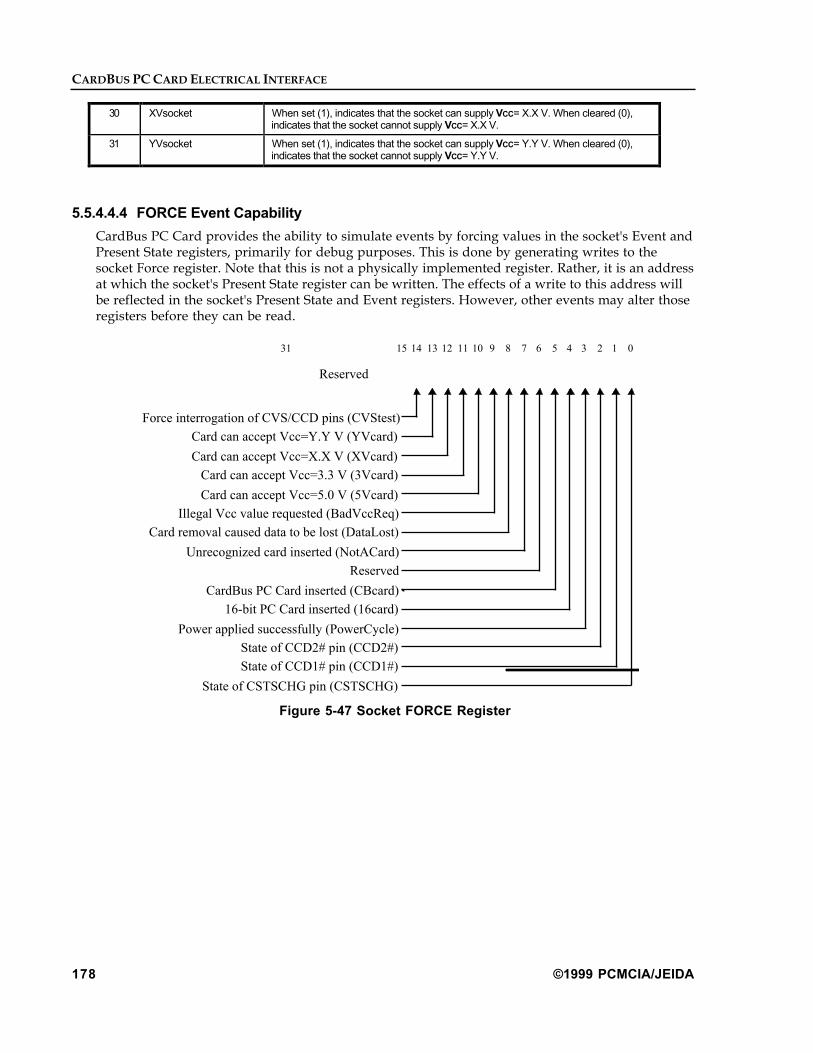
CARDBUS PC CARD ELECTRICAL INTERFACE
178 ©1999 PCMCIA/JEIDA
30 XVsocket When set (1), indicates that the socket can supply VCC= X.X V. When cleared (0),indicates that the socket cannot supply VCC= X.X V.
31 YVsocket When set (1), indicates that the socket can supply VCC= Y.Y V. When cleared (0),indicates that the socket cannot supply VCC= Y.Y V.
5.5.4.4.4 FORCE Event Capability
CardBus PC Card provides the ability to simulate events by forcing values in the socket's Event andPresent State registers, primarily for debug purposes. This is done by generating writes to thesocket Force register. Note that this is not a physically implemented register. Rather, it is an addressat which the socket's Present State register can be written. The effects of a write to this address willbe reflected in the socket's Present State and Event registers. However, other events may alter thoseregisters before they can be read.
Reserved
Card can accept Vcc=Y.Y V (YVcard)
Card can accept Vcc=X.X V (XVcard)
Card can accept Vcc=3.3 V (3Vcard)
Card can accept Vcc=5.0 V (5Vcard)
Illegal Vcc value requested (BadVccReq)
Card removal caused data to be lost (DataLost)
Unrecognized card inserted (NotACard)
Reserved
CardBus PC Card inserted (CBcard)
16-bit PC Card inserted (16card)
Power applied successfully (PowerCycle)
State of CCD2# pin (CCD2#)
State of CCD1# pin (CCD1#)
State of CSTSCHG pin (CSTSCHG)
0123456789101112131431 15
Force interrogation of CVS/CCD pins (CVStest)
Figure 5-47 Socket FORCE Register

ELECTRICAL SPECIFICATION
© 1999 PCMCIA/JEIDA 179
Table 5Ð30 Socket FORCE Register Fields
Bit Field Name Description
0 CSTSCHG Writing a 1 to this field simulates the assertion of the CSTSCHG pin. This results inthe Event register's CSTSCHG field being set. Note that the CSTSCHG field in thePresent State register is not affected and continues to reflect the present state of theCSTSCHG pin. Writing a 0 has no meaning.
1 CCD1# Writing a 1 to this field causes the CCD1# field in the Event register to be set. Notethat the CCD1# field in the Present State register is not affected and continues toreflect the present state of the CCD1# pin. Writing a 0 has no meaning.
2 CCD2# Writing a 1 to this field causes the CCD2# field in the Event register to be set. Notethat the CCD2# field in the Present State register is not affected and continues toreflect the present state of the CCD2# pin. Writing a 0 has no meaning.
3 PowerCycle Writing a 1 to this field simulates the successful completion of a power cycle event bycausing the PowerCycle field in the Event register to be set. Note that thePowerCycle field in the Present State register is not affected and continues to reflectthe present state of the interface power. Writing a 0 has no meaning.
4 16card Writes to this field cause the 16-bit PC Card field in the Present State register to bewritten. If a card is present in the socket (i.e. CCD1# and CCD2# are asserted),writes to this bit field are ignored.
5 CBcard Writes to this field cause the CBcard field in the Present State register to be written. Ifa card is present in the socket (i.e. CCD1# and CCD2# are asserted), writes to thisbit field are ignored.
6 Reserved This field is reserved for future use.
7 NotACard Writes to this field cause the NotAcard field in the Present State register to be written.If a card is present in the socket (i.e. CCD1# and CCD2# are asserted), writes to thisbit field are ignored.
8 DataLost Writes to this field cause the DataLost field in the Present State register to be written.
9 BadVccReq Writes to this field cause the BadVccReq field in the Present State register to bewritten.
10 5VCard Writes to this field cause the 5VCard field in the Present State register to be written.Setting this field disables the socket's ability to power up VCC until the CVStest field isset in the Force register.
11 3VCard Writes to this field cause the 3VCard field in the Present State register to be written.Setting this field disables the socket's ability to power up VCC until the CVStest field isset.
12 XVCard Writes to this field cause the XVCard field in the Present State register to be written.Setting this field disables the socket's ability to power up VCC until the CVStest field isset.
13 YVCard Writes to this field cause the YVCard field in the Present State register to be written.Setting this field disables the socket's ability to power up VCC until the CVStest field isset.
14 CVStest When written to a 1, causes the adapter to interrogate the CVS[2::1] and CCD[2::1]#pins and update the nVCard fields in the Present State register. This action also re-enables the socket to power up VCC if the nVCard fields had been previously forced.
15-31 Reserved These fields are reserved for future use.

CARDBUS PC CARD ELECTRICAL INTERFACE
180 ©1999 PCMCIA/JEIDA
5.5.4.4.5 CONTROL Register
This register provides control of what voltages should be applied to VPP[2::1] and VCC.
02346731
Reserved
Vcc Requested (VccControl)
Reserved
Vpp Requested (VppControl)
Figure 5-48 Socket CONTROL Register
Table 5Ð31 Socket CONTROL Register Fields
Bit Name Description
0-2 VppControl This field is used to request VPP[2::1] voltages:
000 Requested VPP[2::1] voltage = power off
001 Requested VPP[2::1] voltage = 12.0 V
010 Requested VPP[2::1] voltage = 5.0 V
011 Requested VPP[2::1] voltage = 3.3 V
100 Requested VPP[2::1] voltage = X.X V
101 Requested VPP[2::1] voltage = Y.Y V
110 Reserved
111 Reserved
3 Reserved This field is reserved for future use.
4-6 VccControl This field is used to request VCC voltages:
000 Requested VCC voltage = power off
001 Reserved
010 Requested VCC voltage = 5.0 V
011 Requested VCC voltage = 3.3 V
100 Requested VCC voltage = X.X V
101 Requested VCC voltage = Y.Y V
110 Reserved
111 Reserved
7-31 Reserved These fields are reserved for future use.
5.5.4.5 VPP[2::1] Power Requirements
VCC, VPP1, and VPP2 must be initially powered up at the voltage indicated by the CVS[2::1] pins.Other voltages can be applied to VPP1 and VPP2 only after the allowed values have beendetermined from the PC Card's Card Information Structure. (See the Metaformat Specification.)However, if the PC Card was previously configured and the socket can guarantee that no cardchange has taken place, VPP[2::1] may be powered up at the desired voltage instead of VCC.

ELECTRICAL SPECIFICATION
© 1999 PCMCIA/JEIDA 181
5.5.4.6 Card Insertion and Removal
5.5.4.6.1 Card Insertion
The CardBus PC Card interface requires Cold socket insertion. This allows the adapter to properlyconfigure its interface to the correct protocol (16-bit PC Card vs. CardBus PC Card) and determinethe correct voltage for VCC. Card Detect, CCD[2::1]#, and Card Voltage Sense, CVS[2::1], signalsare allowed to be active in this cold state, but must not cause any damage to PC Cards and systems.When a PC Card insertion is detected, the adapter must:
1. Debounce the CCD[2::1]# pins when a low on the card detect lines occurs.
2. Interrogate the CVS[2::1] and CCD[2::1]# pins to determine the type of PC Card inserted(CardBus PC Card or 16-bit PC Card) and its VCC requirements. (See 3. Card Type DetectionMechanism). The results will be reflected in the CBcard, 16card, NotACard, and nVCard fieldsof the socket's Present State register.
3. Set up its logic to match the protocol required by the PC Card inserted (16-bit PC Card orCardBus PC Card). If the adapter chose to drive outputs low to the empty socket, it must High-Zor power off all signals25 at this time in preparation for power up activities. No signals may beactively driven High to an unpowered PC Card except CVS1 and CVS2.
4. Notify Card Services that an insertion event occurred by generating a Status Changed interrupt.The adapter must ensure that the interface is setup for the correct card type before the statuschanged interrupt is serviced.
5. Card Services determines the cause of the status changed interrupt (insertion event in thisscenario) by reading the socket's Event register. After identifying the socket, Card Servicesreads the socket's Present State register to obtain PC Card type and VCC requirementinformation. The power up process will not proceed beyond this point until Card Services givespermission. Automatic power up upon insertion, i.e., without software involvement, isforbidden.
W A R N I N G :
If a 16-bit PC Card was inserted, then the adapter should proceed withpowering-up the interface as described in 4.4.16.1 Socket Vcc for CISRead.
1. Card Services notifies Socket Services of the voltage requirements. Socket Services writes theappropriate register(s) in the adapter to specify the requested VCC and VPP[2::1] value.
2. The adapter must keep glitches on the CSTSCHG input from causing the CSTSCHG field to beset in the socket's Event register during the power-up process by disabling this field. This mustbe done from card insertion until the "Power Up Complete" condition is reached.
3. If the requested voltage is supported by the PC card and can be supplied to the socket, theadapter applies that voltage to the socket's VCC and VPP[2::1]26 pins. If the requested voltage isoutside the range decoded from the card's CVS[2::1] pins or is not available in the system, theadapter must set the BadVccReq field in the socket's Present State register and must not applypower to the VCC pins. When servicing the status changed interrupt, Card Services must alsoread the socket's Present State register to ensure power was successfully applied. Note that this
25CVS1 and CVS2 must not be set to a High-Z state or the CCD# pins will indicate a card removal event for
CardBus PC Cards. If a CardBus PC Card was inserted, CRST# must be driven low.26The requirements for applying power to Vpp are specified in 5.5.4.5 Vpp[2::1] Power Requirements.

CARDBUS PC CARD ELECTRICAL INTERFACE
182 ©1999 PCMCIA/JEIDA
requires the adapter to be aware of the voltages available so that illegal requests can bedetected. CRST# must remain asserted throughout the power up process.
4. The adapter sets the PowerCycle field in the socket's Event register to cause a status changedinterrupt to inform Card Services that the power up process is complete. Note that if an illegalvoltage was requested, no power up will actually occur.
5. After recognizing that the power up process is complete, Card Services clears the socket'sEVENT Register to eliminate spurious interrupt events arising from powering up the interface(e.g., glitches on CSTSCHG from CardBus PC Cards not supporting remote wakeup).
6. Card Services instructs the socket to negate CRST#. Note that software must ensure that thetimings outlined in 5.3 CardBus PC Card Electrical Specification have been met. Also, softwarealone controls the negation of CRST# but hardware will automatically assert CRST# in mostcircumstances.
7. Card Services proceeds with the CardBus PC Card configuration process as defined in 5.4CardBus PC Card Programming Model. (See also the Card Services Specification.)
5.5.4.6.2 Card Removal
CardBus PC Card adapters must consider a PC Card removed when either of the CCD[2::1]# signalsis negated, even if only momentarily. When this condition is detected and a 16-bit PC Card ispresent, the adapter must take action as defined in 4.4.1.7 Socket Vcc for CIS Read. If a CardBus PCCard is present, the adapter must:
1. Immediately idle the bus by asserting CRST# even if the final data phase has not beencompleted, driving CGNT# high, and driving CFRAME# high one clock later to allow for aturn-around cycle. This immediate assertion is necessary since contact bounce issues make itimpossible to reliably execute cycles across the interface. CRST# must remain assertedthroughout the power down process.
Only by physically locking the card in, or providing an imminent removal indication, cancycles be reliably completed and the need to immediately assert CRST# be avoided. Note thatthe imminent removal warning must occur at least 256 CCLK periods before card removalbegins.
2. Drive CAD, CCBE[3::0]#, CPAR, CVS1, and CVS2 low, in addition to CRST#, and set theother outputs to a High-Z state. The adapter must not drive any signal High to an unpoweredsocket.
3. Disable the socket's remote wakeup capability by clearing the CSTSCHG field in the socket'sMask register. The adapter must also disable the CSTSCHG field in the socket's Event registerto keep glitches on CSTSCHG from causing false status changed events. This action could betaken in parallel with steps 1-3.
4. Remove power, VCC and VPP[2::1], from the connector. This action must be automatic; it mustnot wait for the involvement of software. Note that CGNT# must be set to a High-Z state ordriven low before power is removed.
5. Update the CCD1# and CCD2# fields in the socket's Present State register to set correspondingfields in the socket's Event register and generate a status changed interrupt notifying CardServices of the removal event. If a transaction on the CardBus PC Card interface was aborted bythe CRST# assertion or data was stranded in the adapter's buffers, the adapter must also set theDataLost field in its Present State register.

ELECTRICAL SPECIFICATION
© 1999 PCMCIA/JEIDA 183
The dynamic removal of a card creates a window of time, between theremoval event and when the status changed interrupt is serviced, whereclients may attempt to access non-existent resources. In many systems, theattempted accesses must be completed before pending interrupts can beserviced. This means that the adapter must accept writes to the removedcard and return "false" data on reads (all one's for x86 architecture systems)from it. If a new card is inserted, the adapter would have to continueaccepting transactions to the previous card but not forwarding them on. Theonly exception is in systems which provide another mechanism to deal withaccesses during this status changed interrupt latency window.
When a socket is in the Cold state, any externally powered CardBus PC Card must appear at theCardBus PC Card interface like a CardBus PC Card without an external power source. Oneexception to this rule is for CSTSCHG which can be driven across the interface by CardBus PCCards complying with the remote system wakeup protocol.
5.5.4.7 Power Cycling the Interface
It is recommended for the host system to discharge the CardBus PC Card connector's VCC andVPP[2::1] to ground as soon as the power is switched off. Further, care should be taken whendynamically changing the voltage applied to VCC or VPP[2::1] so that power supply shorts do notoccur. The safest implementation is to ensure that all power supply changes transition through 0V.
5.5.4.7.1 Signal Requirements
When powering up or powering down the CardBus PC Card interface, the adapter must holdCRST# asserted throughout the process. (See 5.3.3.2 Reset.) The CardBus PC Card adapter's inputsmust not react to voltages on its inputs for the duration of the power up or power down process(except for the CCD[2::1]# and CVS[2::1] pins).
When CRST# is asserted, the interface signals must be driven to their benign state. (See 5.1.2Signal/Pin Description.) After the interface has been powered down, the adapter may drive theinterface signals low. The adapter must not drive any signal High to an unpowered socket.
5.5.4.7.2 CSTSCHG Requirements
The adapter must default to ignoring the CSTSCHG signal during the power up and power downprocedures. This is necessary because CardBus PC Cards which don't implement remote wakeupmay glitch this pin while VCC transitions. However, this could cause a remote wakeup pulse to bemissed during power down events. Therefore, if the adapter supports remote wakeup and theCardBus PC Card in the socket has implemented it, Card Services, either on its own or at thedirection of a client, must explicitly enable this capability. The adapter reverts to this default modewhenever it is reset or the CardBus PC Card is removed.
5.5.4.7.3 In-Rush Current
During the PC Card power up process, a significant amount of capacitance will be instantaneouslyadded to the power supply's load, drawing a large amount of current. This is referred to as "in-rush"current. It is the responsibility of the system designer to ensure that this does not pull VCC out of itsspecified tolerance range by either current limiting the supply to the socket or other appropriatemeans.
CARDBUS PC CARD ELECTRICAL INTERFACE
184 ©1999 PCMCIA/JEIDA
5.5.4.8 Required Pins
The implementation of CAUDIO is recommended but not required. All other signals are required.(See 5.1.2 Signal/Pin Description.)
However, a simplified implementation is allowed for CCLKRUN#. If the adapter is implemented ina system which will not stop the clock, the adapter may simply assert CCLKRUN# when CRST# isnot asserted and set CCLKRUN# set to a High-Z state when CRST# is asserted.
5.5.4.9 Clock Stopping Support
CardBus PC Card adapters that are going to participate in the clock control protocol (CCLKRUN#)must be able to communicate with the clock source. The mechanisms required are system busdependent but the following behavior must be present in all adapters:
1. The adapter must be able to restart CCLK when a transaction originates on the system bus, oranother CardBus PC Card, and needs to cross the affected CardBus PC Card interface.
2. The adapter must forward "don't stop the clock" requests from the CardBus PC Card to the clocksource in a manner that ensures the clock stream isn't interrupted when the CardBus PC Cardmeets the CCLKRUN# specification.
3. The adapter must ensure that the latency involved in restarting the clock doesn't become visibleto software. Note that this has implications on the system design since the adapter doesn'tnecessarily have full control of the clock resource.
4. The adapter must not allow the clock to stop before the time specified in the CCLKRUN#protocol.
5.5.4.10 Special Cycle Support
CardBus PC Card adapters do not have to respond to, or generate special cycles on the CardBus PCCard interface. This capability has been defined to allow communication in the event sufficient pinsdo not exist on the interface.
5.5.4.11 Actions When Adapter Is Reset
When the system resets the CardBus PC Card adapter, the adapter must:
1. Quit accepting transactions on its system bus and CardBus PC Card interfaces.
2. Flush write buffers to its CardBus PC Card interfaces. Flush read buffers when the masterresides on one of its CardBus PC Card interfaces. Any read data intended for masters elsewherein the system should be deleted.

ELECTRICAL SPECIFICATION
© 1999 PCMCIA/JEIDA 185
6 . P C I B U S P O W E R M A N A G E M E N T I N T E R F A C E
F O R C A R D B U S C A R D S
6.1 IntroductionSince its introduction in 1993, PCI has become a very popular bus. It is used in a wide variety ofcomputer systems sold today ranging from laptops to large servers. Its bandwidth and efficientsupport for multiple masters has allowed it to sustain high performance applications while at thesame time, its low pin count and high integration factor has enabled very low cost solutions.
Power Management in the current PC platform is performed by a combination of BIOS and SystemManagement Mode (SMM) code utilizing hardware unique to each platform. While this strategy hassuccessfully brought the PC platform into the mobile environment it is beset with problems becauseof the fact that there is no standard way to truly determine when the system is busy and when it isactually idle. The operating system does have this information so it makes sense to give it theresponsibility for power management. The reason that this has not happened up to now is a lack ofstandards to provide the operating system with the required information that would allow it tocontrol the hardware in a platform independent way. This specification addresses this need.
While the PCI Local Bus Specification is quite complete with a solid definition of protocols, electricalcharacteristics and mechanical form factors, no provision was made in the original specification forsupporting power management functionality. This specification addresses this requirement bydefining four distinct power states for the PCI bus and four distinct power states for PCI functions aswell as an interface for controlling these power states.
6.1.1 Goals of this SpecificationThe goal of this specification is to establish a standard set of PCI peripheral power managementhardware interfaces and behavioral policies. Once established this infrastructure enables anoperating system to intelligently manage the power of PCI functions, and buses.
Detailed Goals for PCI Power Management Interface:
• Enable multiple PCI function power levels
• Establish a standard for PCI function wakeup events
• Establish a standard for reporting power management capabilities
• Establish a standard mechanism for controlling a PCI function's power state
• Establish a standard mechanism for controlling a PCI bus's power state
• Minimal impact to the PCI Local Bus Specification
• Backwards compatible with PCI Bus Revision 2.1, and 2.0 compliant designs
• Preserve the designerÕs ability to deliver differentiated products
• Provide a single architecture for all markets from mobile through server

PCI BUS POWER MANAGEMENT INTERFACE FOR CARDBUS CARDS
186 ©1999 PCMCIA/JEIDA
Key Attributes of this Specification:
• Enhances the PCI BusÕs Plug and Play capabilities by comprehending power management.
• Standardized power state definitions
• Standardized register interface in PCI configuration space
• Standardized wake events
6.1.2 Target AudienceThis chapter is intended to address the needs of developers of CardBus cards. This chapter describesthe hardware requirements of such devices to allow the power management of those devices in anoperating system directed power management environment.
Software developers are also a targeted audience for this specification. Specifically, developers ofoperating systems and device drivers need to understand the power management interfacespresented by compliant devices to be able to manage them.
6.1.3 Overview/ScopeIn order to implement a power managed system under the direction of the operating system, alarge array of tightly coupled hardware, and software ingredients needs to be defined andintegrated. The following diagram outlines, at a high level, this set of required architecturalbuilding blocks.

ELECTRICAL SPECIFICATION
© 1999 PCMCIA/JEIDA 187
OSPM specifications. Device driversspecifications. PM policy specifications
Platform ArchitectureIntegration
Specification
I/O BusPower Management
Specifications
USB
IEEE1394
PCI
Device-ClassPower Management
Specifications
Audio
Storage
Graphics
PCI toCardBusBridge
Function
SCOPE ofSpecification
Config Regs Config Regs
Function
Config Regs
Host PCI Bus
CardBus CardBus
Figure 6-1: Operating System Directed Power Management System Architecture
The scope of this specification is sharply focused on establishing a standard set of interfaces that arerequired to power manage PCI-to-CardBus Bridges, buses, devices, CardBus cards and functions.
Any PCI based component can use the mechanisms described in this specification.
Devices which can only be implemented on the motherboard are power managed in motherboard-specific ways (such as ACPI), and as such, fall outside the scope of this specification. Dockingbridges, for example fall into the motherboard devices category because the physical dockingbridge component always resides logically on the motherboard, and is never deployed as an add-incard. As such Docking bridges are not covered by this specification.
The PCI Bus Power Management Interface Specification describes requirements for implementingpower management for PCI functions which are capable of being used on an add-in card.

PCI BUS POWER MANAGEMENT INTERFACE FOR CARDBUS CARDS
188 ©1999 PCMCIA/JEIDA
6.1.4 Glossary of TermsBus Segment Reset Bus Segment Reset is defined as the hardware reset signal that is taken as actual physical
input to a given component within a system. The Bus Segment Reset signal for a CardBuscard is the CRST# signal.
Legacy PCI Devices A class of CardBus cards built before the PCI Bus Power Management Interface Specificationfor CardBus was added to the PC Card Standard and are PC Card Standard February1995 compliant. Legacy CardBus cards are assumed to be in the D0 power managementstate whenever power is applied to them.
Operating System Throughout this specification, the terms ÒOperating SystemÓ and Òsystem softwareÓ refer tothe combination of power management services, device drivers, user mode services, and/orkernel mode services.
Originating Device From the perspective of the operating system (Host CPU), the first bridge componentencountered with a PCI bus downstream of it is defined as the Originating Device for that PCIbus segment. For a CardBus card, the originating device is the PCI-to-CardBus bridgecontrolling its bus (see figure below)
CPU
Host Bridge
PCI to CardBusBridge
Primary Bus I/F
Secondary Bus I/F
PCI Bus I/F
PCI Bus(0)
CardBus bus
Originating Devicefor bus(0)
Originating Devicefor CardBus bus
Host Bus I/F
Figure 6-2: Example "Originating Devices"

ELECTRICAL SPECIFICATION
© 1999 PCMCIA/JEIDA 189
PCI-to-CardBus Bridge PCI-to-CardBus bridges couple the PCI bus and the CardBus bus together. They arecharacterized by a primary bus interface, and a secondary bus interface.
CardBus card (or device) A physical card consisting of one load on the CardBus bus. This single CardBus card maycontain up to 8 CardBus Functions.
CardBus Function A set of functionality inside a CardBus card represented by one 256 byte configuration space.Each CardBus function within a device generally has a separate software driver.
PCI Function Context The variable data held by the CardBus function, usually volatile. Function context refers tosmall amounts of information held internal to the function. Function Context is not limited onlyto the contents of the functionÕs PCI registers, but rather refers also to the operational states ofthe function including state machine context, power state, execution stack (in some cases),etc. For example, for a PCI-to-CardBus Bridge, the internal status and mask registers and theVcc control signals would be a special case of Function Context which must be preserved.
PME Context Power Management Event Context is defined as the functional state information and logicrequired to generated Power Management Events (PMEs), report PME status, and enablePMEs.
Power Management Mechanisms in software and hardware to minimize system power consumption, managesystem thermal limits and maximize system battery life. Power management involvestradeoffs among system speed, noise, battery life, and AC power consumption.
Power Management Event (PME) A power management event is the process by which a CardBus function can request achange of its power consumption state. Typically a device uses a PME to request a changefrom a power savings state to the fully operational (and fully powered) state. However, adevice could use a PME to request a change to a lower power state. A power managementevent is requested via the assertion of the PME# signal. For a CardBus card, assertion ofCSTSCHG (and STSCHG# for a PC Card) are translated to the host systemÕs PME#through the PCI-to-CardBus bridge . The power management policies of the systemultimately dictate what action is taken as a result of a power management event.
Primary or Ordinate Bus The primary bus of a CardBus card refers to the bus that is topologically closest to the CPUthat is running the operating system.
Restore Time Restore time is defined as the time required to fully restore a CardBus function to its fullyoperational state from a power saving mode of operation. It is measured as the total elapsedtime between when the system software request for restoration occurs to when the function isfully configured and activated.
Secondary or Subordinate Bus The secondary bus of a CardBus card refers to the bus that is topologically farthest from theCPU that is running the operating system.
Sleeping State A computer state where the computer consumes a small amount of power, user modethreads are not being executed, and the system ÒappearsÓ to be off (from an end userÕsperspective, the display is off, etc.). Latency for returning to the Working state varies on thewakeup environment selected prior to entry of this state (for example, should the systemanswer phone calls, etc.). Work can be resumed without rebooting the OS because largeelements of system context are saved by the hardware and the rest by system software. It isnot safe to disassemble the machine in this state.
Soft Off State A computer state where the computer consumes a minimal amount of power. No user modeor system mode code is run. This state requires a large latency in order to return to theWorking state. The systemÕs context will not be preserved by the hardware. The systemmust be restarted to return to the Working state. It is not safe to disassemble the machine.
Wakeup Event An event which can be enabled to wake the system from a Sleeping or Soft Off state to aWorking state to allow some task to be performed.
Working State A computer state where the system dispatches user mode (application) threads and theyexecute. In this state, devices (peripherals) are dynamically having their power statechanged. The user will be able to select (through some user interface) variousperformance/power characteristics of the system to have the software optimize forperformance or battery life. The system responds to external events in real time. It is not safeto disassemble the machine in this state.
6.1.5 Related DocumentsPCI Local Bus Specification, Revision 2.1, June 1, 1995, PCI Special Interest Group
PCI to PCI Bridge Architecture Specification, Revision 1.0, April 5, 1994, PCI Special InterestGroup
PCI Mobile Design Guide, Revision 1.0, October 27, 1994, PCI Special Interest Group

PCI BUS POWER MANAGEMENT INTERFACE FOR CARDBUS CARDS
190 ©1999 PCMCIA/JEIDA
PCI Bus Power Management Specification, Revision 1.0, Mar 18, 1997, PCI Special Interest Group
PC Card Standard, April 1998 (Release 6.1), PCMCIA/JEIDA
Advanced Configuration and Power Interface Specification Revision 1.0, Intel Corporation,Microsoft Corporation and Toshiba
Toward the ÒOnNowÓ Machine: The Evolution of the PC Platform, Microsoft Technology Brief,April 1996, Microsoft Corporation
Device Power Management, Microsoft Technology Brief, April 1996, Microsoft Corporation
Device Class Power Management Reference Specifications, Draft Proposals, 1996, MicrosoftCorporation
OnNow Design Initiative and ACPI, Microsoft Web Page with links to many of the documentsabove, 1996, Microsoft Corporation
OnNow Power Management and the Win32 Driver Model, 1996, Microsoft Corporation
PCI Hot-Plug Specification, PCI Special Interest Group
6.1.6 Conventions Used in this ChapterSeveral conventions are used in this chapter to help make it more readable. These are listed below.
• Power states are shown in bold italic text as in D0.
• Register names are shown in bold text as in PMCSR.
• Names of bits or fields within registers are in italic text as in PowerState.
• Signal names are all capitalized and bold as in PME#.
• All numbers are represented in decimal unless followed by a small letter.
• Hexadecimal numbers are represented with a following ÒHÓ (e.g. DCH).
• Binary numbers are represented with a following ÒBÓ (e.g. 10B).
6.2 CardBus Power Management Overview
6.2.1 CardBus Power Management StatesPower management states are defined as varying, distinct levels of power savings. PowerManagement states are denoted by a state number. Throughout this chapter power managementstates for both CardBus buses and CardBus functions will be defined, specified and discussed. Powermanagement states for PCI buses, by convention, are prefixed with a ÒBÓ, and end in the powermanagement state number (0-3). The higher the number the more aggressive the intended powersavings. Similarly for CardBus functions the power management state is prefixed with a ÒDÓ, andends with the power management state number (0-3). Intended power savings increase with thepower management state number.
6.2.1.1 CardBus Function Power States
Up to four power states are defined for each CardBus function in the system. These are D0-D3 withD0 being the maximum powered state, and D3 being the minimum powered state. D1 and D2power management states enable intermediate power savings states between the D0 (on) and D3(off) power management states.

ELECTRICAL SPECIFICATION
© 1999 PCMCIA/JEIDA 191
While the concept of these power states is universal for all functions in the system, the meaning, orintended functional behavior when transitioned to a given power management state is dependentupon the type (or class) of the function.
6.2.1.2 Bus Power States
The power management state of a bus can be characterized by certain attributes of the bus at agiven time such as whether or not power is supplied, the speed of the clock, and what types of busactivities are allowed. These states are referred to as B0, B1, B2 and B3.
This specification defines a mechanism that enables explicit control of a CardBus busÕ power andCardBus clock as a function the power management state of its originating device. The mechanismcan be disabled (see 6.3.2.5 PMCSR_BSE - PMCSR PCI-to-PCI Bridge Support Extensions(Offset=6) Ð Not Used in CardBus Cards - Reserved, and 6.4.7.1 Control of Secondary Bus PowerSource and Clock).
6.2.1.3 Device-Class Specifications
The PCI Bus Power Management Interface Specification standardizes the power managementhardware interface for the CardBus Bus, and CardBus cards. However CardBus functions belongingto different device classes may behave differently when operating in the same power managementstate. This is the notion of Device-Class specific power management policy. For example, the list ofcapabilities that an audio subsystem would support in a given power management state would mostlikely be different than the list of capabilities supported by a graphics controller operating in thesame power management state.
While Device-Class Power Management Specifications fall outside the scope of this specification,they are mentioned here to inform the reader of their important relationship to the interfacesdefined in this chapter. Each class of device must have its own class specific set of powermanagement policies to define their intended behavior while in each of the power managementstates.
For a fully integrated power management system, these class-specific power management policiesmust also be standardized. Each major device type must have a ÒDevice-Class Power ManagementSpecificationÓ that all manufacturers can use as a guide to facilitate the seamless integration of theirpower managed products into a system.

PCI BUS POWER MANAGEMENT INTERFACE FOR CARDBUS CARDS
192 ©1999 PCMCIA/JEIDA
Device-Class Specifications will generally cover the following areas:
Device-class power characteristics Each class of CardBus function should have a standard definition for each function powermanagement state. This should include target power consumption levels, command responselatencies, and state-change latencies. Implementation details for achieving these levels (suchas whether an entire functional block is powered-off or the clock is stopped) might beimportant to a particular device class and, if so, should be specified. If any of thesecharacteristics are in conflict with the requirements of the bus specifications, the function maynot be able to implement that state on that particular bus.
Minimum Device-Class powercapabilities
Each class of CardBus function should have a standard set of power capabilities appropriateto the class. An example might be to require support either for all four power states or forsome lesser number. Requirements might also be specified for accuracy and frequency ofpower status updates. Finally, there might be class-specific requirements for Wakeupcapabilities. For example, all modems should be able to wake the PC from D1, and so on.
Device-class functionalcharacteristics
Each class of CardBus function should have a standard definition of the available subset offunctioning capabilities and features in each power state. For example, the network adaptercan receive, but cannot transmit; the sound card is fully functional except that the power ampsare off; and so on.
Device-class Wakeup characteristics Each class of CardBus function should have a standard definition of its Wakeup policy,including a recommended resume latency specification. This includes specifying the variousclass-specific events that can wake up the system, and the power states from which theWakeup can be signaled, with implementation details and examples where appropriate.
6.2.1.4 Bus Support for CardBus Function Power Management
Four base capabilities enable a robust power management solution. The capabilities are defined as:
Get Capabilities operation This operation informs the operating system of the power management capabilities andfeatures of a given function. It is performed as a part of the Operating SystemÕs deviceenumeration27 and uses the information it receives to help determine the power managementpolicies to implement in the system. Information required from the function include whichpower states are implemented, and the functionÕs Wakeup capabilities.
Set Power State operation This operation puts the function into a specific power management state and enables powermanagement features based on the global system power management policy and thefunctionÕs specific capabilities. This includes setting the function to wake the system from asleeping state if certain events occur.
Get Power Status operation This operation returns information about the current power state of the CardBus function.
Wakeup operation This is a mechanism for having a CardBus function wake the system from a sleeping state onspecified events.
While individual CardBus functions must support only the first three capabilities with wakeupbeing optional, all basic power management operations must be supported by the bus architectureto ensure that CardBus functions on the bus can be power managed.
For multi-function CardBus cards there is a common portion of bus interface logic that physicallybinds each of the supported functions to the CardBus bus. This common logicÕs power consumptionis explicitly reported if supported, using the Data register of Function 0. For further detail on thereporting of CardBus function power consumption, see 6.3.2.6 Data (Offset = 7).
Control of the common logic is handled by the multi-function device in a software transparentfashion. For further power savings in a runtime environment, the enabling and disabling of someportion of this common CardBus bus interface logic is the responsibility of the multi-functioncomponent hardware. This implicit power control, if implemented, may be based upon the powerstates of the functions behind it. As an example one might consider a hardware administered logiccontrol policy where the common logic can not be internally powered down unless all of thefunctions hosted by the device have been placed in the D3hot state first.
27 The CardBus function provides power management capabilities reporting through a standard register definition
as specified in this document.

ELECTRICAL SPECIFICATION
© 1999 PCMCIA/JEIDA 193
6.3 CardBus Power Management InterfaceThe four basic power management operations that have been defined are: Capabilities Reporting,Power Status Reporting, Setting Power State and System Wakeup. Of these four capabilities all arerequired of each function with the exception of wakeup event generation. This section describes theformat of the registers in CardBus configuration space which are used by these operations.
The Status and Capabilities Pointer (Cap_Ptr) fields have been highlighted to indicate where thePCI Power Management features appear in the standard Configuration Space Header.
Device ID Vendor ID 00h
Status (with bit 4 set to 1) Command 04h
Class Code Revision ID 08h
BIST Header Type Latency Timer Cache Line Size 0Ch
10h
14h
Base Address Registers 18h
1Ch
20h
24h
CardBus CIS Pointer 28h
Subsystem ID Subsystem Vendor ID 2Ch
Expansion ROM Base Address 30h
Reserved Cap_Ptr(type 0) 34h
Reserved 38h
Max_Lat Min_Gnt Interrupt Pin Interrupt Line 3Ch
Figure 6-3: Standard PCI Configuration Space Header Type 0
Software must have a standard method of determining if a specific function is designed inaccordance with this specification. This is accomplished by using a bit in the CardBus cardÕs PCIStatus register to indicate the presence of the Capabilities List and a single byte in the standardCardBus card PCI Configuration Space Header which acts as a pointer to a linked list of additionalcapabilities. Software can then traverse the list looking for the proper ID for CardBus card PCIPower Management (Cap_ID=01H). If there is no Capabilities List (New Capabilities bit in the Statusregister = 0) or if the list does not contain an item with the proper ID, the function does not supportthe CardBus PCI Power Management interface described in this chapter and the Operating Systemwill assume that the function only supports the D0 and D3cold power management states. TheseLegacy CardBus functions may also require a device specific initialization sequence after anytransition from D3cold to D0 (see 6.8.3 Restoring PCI Functions From a Low Power State).
6.3.1 Capabilities List Data StructureThe New Capabilities bit in the PCI Status Register (offset=06h) indicates whether or not the subjectfunction implements a linked list of extended capabilities. Specifically, if bit 4 is set, the Cap_Ptrregister is implemented to give the offset in configuration space for the first item in the list.

PCI BUS POWER MANAGEMENT INTERFACE FOR CARDBUS CARDS
194 ©1999 PCMCIA/JEIDA
Table 6-1: PCI Status Register
Bits DefaultValue
Read/Write Description
15:05 -- -- Definition given in PCI Local Bus Specification Revision 2.1
04 1B Read Only New Capabilities - This bit indicates whether this function implements a listof extended capabilities such as PCI Power Management. When set this bitindicates the presence of New Capabilities. A value of 0 means that thisfunction does not implement New Capabilities.
03:00 0H Read Only Reserved
The location of the Capabilities Pointer (Cap_Ptr) depends on the CardBus cardÕs PCI header type.See 6.3.1.1 Capabilities List Cap_Ptr Location for Header Type specific Cap_Ptr offsets.
Table 6-2: Capabilities Pointer - Cap_Ptr
Bits DefaultValue
Read/Write Description
07:00 XXH Read Only The Cap_Ptr provides an offset into the functionÕs CardBus cardÕs PCIConfiguration Space for the location of the first item in the Capabilities LinkedList. The Cap_Ptr offset is DWORD aligned so the two least significant bitsare always Ò0Ós.
If a function does not implement any capabilities with IDs defined by the PCI SIG, the NewCapabilities bit in the PCI Status register (bit 4) should read as Ò0Ó and the Cap_Ptr register shouldbe ignored. Values of 00h-3Fh are not valid values for the Cap_Ptr because they point into thestandard CardBus cardÕs PCI header. A CardBus function may choose any DWORD aligned offset asindicated in Table 6-3: PCI Configuration Space Header Type / Cap_Ptr mappings.
0 ID
Capability Y
ID
01h
Cap_Ptr
PM Regs
Capability X
8 bits
Standard PCI Config Header Type 0Offset 34h
Next Item
Next Item
Next Item
Figure 6-4: Capabilities Linked List
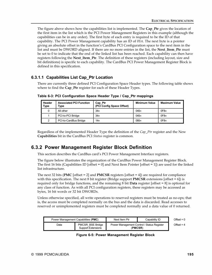
ELECTRICAL SPECIFICATION
© 1999 PCMCIA/JEIDA 195
The figure above shows how the capabilities list is implemented. The Cap_Ptr gives the location ofthe first item in the list which is the PCI Power Management Registers in this example (although thecapabilities can be in any order). The first byte of each entry is required to be the ID of thatcapability. The PCI Power Management capability has an ID of 01H. The next byte is a pointergiving an absolute offset in the functionÕs CardBus PCI Configuration space to the next item in thelist and must be DWORD aligned. If there are no more entries in the list, the Next_Item_Ptr mustbe set to 0 to indicate that the end of the linked list has been reached. Each capability can then haveregisters following the Next_Item_Ptr. The definition of these registers (including layout, size andbit definitions) is specific to each capability. The CardBus PCI Power Management Register Block isdefined in this specification.
6.3.1.1 Capabilities List Cap_Ptr Location
There are currently three defined PCI Configuration Space Header types. The following table showswhere to find the Cap_Ptr register for each of these Header Types.
Table 6-3: PCI Configuration Space Header Type / Cap_Ptr mappings
HeaderType
Associated PCI FunctionType
Cap_Ptr(PCI Config Space Offset)
Minimum Value Maximum Value
0 All other 34H 040H 0F8H
1 PCI-to-PCI Bridge 34H 040H 0F8H
2 PCI-to-CardBus Bridge 14H 080H 0F8H
Regardless of the implemented Header Type the definition of the Cap_Ptr register and the NewCapabilities bit in the CardBus PCI Status register is common.
6.3.2 Power Management Register Block DefinitionThis section describes the CardBus cardÕs PCI Power Management Interface registers.
The figure below illustrates the organization of the CardBus Power Management Register Block.The first 16 bits (Capabilities ID [offset = 0] and Next Item Pointer [offset = 1]) are used for the linkedlist infrastructure.
The next 32 bits (PMC [offset = 2] and PMCSR registers [offset = 4]) are required for compliancewith this specification. The next 8 bit register (Bridge support PMCSR extensions [offset = 6]) isrequired only for bridge functions, and the remaining 8 bit Data register [offset = 8] is optional forany class of function. As with all PCI configuration registers, these registers may be accessed asbytes, 16 bit words or 32 bit DWORDs.
Unless otherwise specified, all write operations to reserved registers must be treated as no-ops; thatis, the access must be completed normally on the bus and the data is discarded. Read accesses toreserved or unimplemented registers must be completed normally and a data value of 0 returned.
Power Management Capabilities (PMC) Next Item Ptr Capability ID Offset = 0
Data PMCSR_BSE BridgeSupport Extensions
Power Management Control / Status Register(PMCSR)
Offset = 4
Figure 6-5: Power Management Register Block

PCI BUS POWER MANAGEMENT INTERFACE FOR CARDBUS CARDS
196 ©1999 PCMCIA/JEIDA
The offset for each register is listed as an offset from the beginning of the linked list item which isdetermined either from the Cap_Ptr (If Power Management is the first item in the list) or theNext_Item_Ptr of the previous item in the list.
6.3.2.1 Capability Identifier - Cap_ID (Offset = 0)
The Capability Identifier, when read by system software as 01H indicates that the data structurecurrently being pointed to is the PCI Power Management data structure. Each function of a PCIdevice may have only one item in its capability list with Cap_ID set to 01H.
Table 6-4: Capability Identifier - Cap_ID
Bits DefaultValue
Read/Write Description
07:00 01H Read Only ID - This field, when Ò01HÓ identifies the linked list item as being the PCIPower Management Registers.
6.3.2.2 Next Item Pointer - Next_Item_Ptr (Offset = 1)
The Next Item Pointer Register describes the location of the next item in the functionÕs capabilitylist. The value given is an offset into the functionÕs CardBus cardÕs PCI Configuration space. If thefunction does not implement any other capabilities defined by the PCI SIG for inclusion in thecapabilities list, or if power management is the last item in the list, then this register must be set to00H.
Table 6-5: Next Item Pointer - Next_Item_Ptr
Bits DefaultValue
Read/Write Description
07:00 00H Read Only Next Item Pointer - This field provides an offset into the functionÕs PCIConfiguration Space pointing to the location of next item in the functionÕscapability list. If there are no additional items in the Capabilities List, thisregister is set to 00H.
6.3.2.3 PMC - Power Management Capabilities (Offset = 2)
The Power Management Capabilities register is a 16 bit read-only register which providesinformation on the capabilities of the function related to power management. The information in thisregister is generally static and known at design time.

ELECTRICAL SPECIFICATION
© 1999 PCMCIA/JEIDA 197
Table 6-6: Power Management Capabilities Ð PMC for CardBus Cards
Bits DefaultValue
Read/Write Description
15:11 DeviceSpecific
Read Only PME_Support - This five bit field indicates the power states in which thefunction may assert PME#. A value of 0B for any bit indicates that the functionis not capable of asserting the PME# signal while in that power state.
bit(11) XXXX1B Ð PME# can be asserted from D0
bit(12) XXX1XB Ð PME# can be asserted from D1
bit(13) XX1XXB Ð PME# can be asserted from D2
bit(14) X1XXXB Ð PME# can be asserted from D3hot
bit(15) 1XXXXB Ð PME# can be asserted from D3cold
10 DeviceSpecific
Read Only D2_Support - If this bit is a Ò1Ó, this function supports the D2 PowerManagement State.
Functions that do not support D2 must always return a value of Ò0Ó for this bit.
09 DeviceSpecific
Read Only D1_Support - If this bit is a Ò1Ó, this function supports the D1 PowerManagement State.
Functions that do not support D1 must always return a value of Ò0Ó for this bit.
08:06 000B Read Only Reserved
05 DeviceSpecific
Read Only DSI - For definition regarding the Device Specific Initialization bit, see the PCIBus Power Management Specification.
04 DeviceSpecific
Read Only Auxiliary Power Source (VAUX) -This bit is only meaningful if bit 15 (D3cold
supporting PME#) is a Ò1Ó. When this bit is also a Ò1Ó it indicates that supportfor PME# in D3cold requires auxiliary power supplied by the system by way ofa the slot Vcc pins and will consume less than 200 mA.
A Ò0Ó in this bit indicates that the function supplies its own auxiliary powersource.
If the function does not support PME# while in D3cold, bit(15)=0, then this fieldmust always return Ò0Ó.
03 0B Read Only PME Clock - When this bit is a Ò1Ó it indicates that the function relies on thepresence of the PCI clock for PME# operation. When this bit is a Ò0Ó itindicates that no PCI clock is required for the function to generate PME#.
Functions that do not support PME# generation in any state must return Ò0Ó forthis field.
02:00 001B Read Only Version - A value of 001B indicates that this function complies with theRevision 1.0 of the PCI Power Management Interface Specification.
6.3.2.4 PMCSR - Power Management Control/Status (Offset = 4)
This 16 bit register is used to manage the PCI functionÕs power management state as well as toenable/monitor power management events.
The Power Management Event support bits, PME_Status, and PME_En, are defined to be ÒstickyÓbits for functions that can generate power management events from D3cold, in that their states arenot affected by power on reset or transitions from D3cold to the D0 Uninitialized state. Preservation ofthese bits is typically achieved by either powering them with an auxiliary power source, or byusing non-volatile storage cells for them. The only way to clear out these bits is to have systemsoftware write to them with the appropriate values. For a CardBus card, setting PME_En in state D0really performs no additional function other than causing the CSTSCHG signal to be latched intothe PME_Status field of the PMCSR. However, in states D1, D2 and D3xxx, CSTSCHG can not beasserted unless PME_En is set. Again, this causes CSTSCHG, the CardBus cardÕs PME# signal, tobe latched into the PMCSRÕs PME_Status bit. These bits follow the ÒstickyÓ rules associated with anyPCI device. Only a software write to each bit or complete removal of all Vcc voltages, includingVAUX, will cause these bits to change state from a Ò1" to a "0".

PCI BUS POWER MANAGEMENT INTERFACE FOR CARDBUS CARDS
198 ©1999 PCMCIA/JEIDA
As mentioned previously, the PME Function Context is defined as the logic responsible foridentifying power management events, the logic responsible for generating the PME# (CSTSCHG)signal and the bits within this register that provide the standard system interface for thisfunctionality. PME Function Context also contains any device class specific status that must survivethe transition to the D0 Uninitialized state as well.
If a function supports PME# (CSTSCHG) generation from D3cold, its PME Function Context is notaffected by either a CardBus slot reset, CRST#, (hardware component reset), or the internal "soft" re-initialization that occurs when restoring a device from D3hot. This is because the functionÕs PowerManagement Event functionality itself may have been responsible for the wake event which causedthe transition back to D0. Therefore, the PME Function Context must be preserved for the systemsoftware to process.
If PME# (CSTSCHG) generation is not supported from D3cold then all PME Function Context isinitialized with the assertion of a bus segment reset.
Because a CardBus bus CRST# assertion does not necessarily clear all functionsÕ PME FunctionContext, (functions that support PME# (CSTSCHG) from D3cold), the system software is required toexplicitly initialize all PME Function Context, including the Power Management Event support bits,for all functions during initial operating system load. In terms of the PMCSR this means that duringthe initial operating system load each functionÕs PME_En bit must be written with a "0", and eachfunctionÕs PME_Status bit must be written with a "1" by system software as part of the process ofinitializing the system.

ELECTRICAL SPECIFICATION
© 1999 PCMCIA/JEIDA 199
Table 6-7: Power Management Control/Status - PMCSR
Bits Value at Reset Read/ Write Description
15 Sticky Bit,indeterminate attime of initial OSboot if functionsupports PME#(CSTSCHG) fromD3cold.
0B, if the functiondoes not supportPME#(CSTSCHG) fromD3cold.
Read/ Write-Clear
PME_Status - This bit is set when the function would normally assert thePME# (CSTSCHG) signal independent of the state of the PME_En bit.
Writing a "1" to this bit will clear it and cause the function to stop assertinga PME# (CSTSCHG) (if enabled). Writing a "0" has no effect.
This bit defaults to "0" if the function does not support PME# (CSTSCHG)generation from D3cold.
If the function supports PME# (CSTSCHG) from D3cold then this bit issticky and must be explicitly cleared by the operating system each time theoperating system is initially loaded.
14:13 Device Specific Read Only Data_Scale - This two bit read-only field indicates the scaling factor to beused when interpreting the value of the Data register. The value andmeaning of this field will vary depending on which data value has beenselected by the Data_Select field.
This field is required for CardBus cards.
See 6.3.2.6 Data (Offset = 7)for more details.
12:09 0000B Read Write Data_Select - This four bit field is used to select which data is to bereported through the Data register and Data_Scale field.
This field is required for CardBus cards.
See 6.3.2.6 Data (Offset = 7)for more details.
08 Sticky Bit,indeterminate attime of initial OSboot if functionsupports PME#(CSTSCHG) fromD3cold.
0B, if the functiondoes not supportPME#(CSTSCHG) fromD3cold.
Read/ Write PME_En - "1" enables the function to assert PME# (CSTSCHG). When"0" PME# (CSTSCHG) assertion is disabled.
This bit defaults to "0" if the function does not support PME# generationfrom D3cold.
If the function supports PME# (CSTSCHG) from D3cold then this bit issticky and must be explicitly cleared by the operating system each time theoperating system is initially loaded.
07:02 000000B Read Only Reserved
01:00 00B Read/ Write PowerState - This two bit field is used both to determine the current powerstate of a function and to set the function into a new power state. Thedefinition of the field values is given below.
00B - D0
01B - D1
10B - D2
11B - D3hot
If software attempts to write an unsupported, optional state to this field, thewrite operation must complete normally on the bus, however the data isdiscarded and no state change occurs.
6.3.2.5 PMCSR_BSE - PMCSR PCI-to-PCI Bridge Support Extensions (Offset=6) ÐNot Used in CardBus Cards - Reserved
PMCSR_BSE supports PCI bridge specific functionality and is required for all PCI-to-PCI and PCI-to-CardBus bridges.

PCI BUS POWER MANAGEMENT INTERFACE FOR CARDBUS CARDS
200 ©1999 PCMCIA/JEIDA
Table 6-8: PMCSR Bridge Support Extensions - PMCSR_BSE
Bits Value atReset
Read/Write Description
07 0 Read Only BPCC_En (Bus Power/Clock Control Enable) - Reserved
06 0 Read Only B2_B3# (B2/B3 support for D3hot) - Reserved
05:00 000000B Read Only Reserved
6.3.2.6 Data (Offset = 7)
The Data Register is an 8 bit read-only register that provides a mechanism for the function to reportstate dependent operating data such as power consumed or heat dissipation. Typically the datareturned through the Data register is a static copy (look up table, for example) of the functionÕsworst case "DC characteristics" data sheet. This data is required for CardBus cards.
Any type of data could be reported through this register, but only power usage is defined by thisversion of the specification. The Data_Select and Data_Scale fields must also be implemented.
Table 6-9: Data Register
Bits DefaultValue
Read/Write Description
07:00 00H Read Only Data - This register is used to report the state dependent data requested bythe Data_Select field. The value of this register is scaled by the value reportedby the Data_Scale field.
The Data register is used by writing the proper value to the Data_Select field in the PMCSR andthen reading the Data_Scale field and the Data register. The binary value read from Data is thenmultiplied by the scaling factor indicated by Data_Scale to arrive at the value for the desiredmeasurement. The table below shows which measurements are defined and how to interpret thevalues of each register.

ELECTRICAL SPECIFICATION
© 1999 PCMCIA/JEIDA 201
Table 6-10: Power Consumption/Dissipation Reporting
Value in Data_Select Data Reported Data_ScaleInterpretation
Units/Accuracy
0 D0 Power Consumed
1 D1 Power Consumed
2 D2 Power Consumed 0 = Unknown
3 D3 Power Consumed 1 = 0.1x Watts
4 D0 Power Dissipated 2 = 0.01x
5 D1 Power Dissipated 3 = 0.001x
6 D2 Power Dissipated
7 D3 Power Dissipated
8 Common logic powerconsumption (Multi-function PCIdevices, Function 0 only)
9-15 Reserved (function 0 of a multi-function device)
0 = Unknown 1-3 = TBD TBD
8-15 Reserved (single function PCIdevices, and other functions(greater than function 0) within amulti-function device)
0 = Unknown 1-3 = TBD TBD
When using the Data register as a window into the data sheet for the PCI function, data returnedmust comply with measurements derived from the following test environment:
• Bus Frequency: 33 MHz
• VCC: 3.3 VDC
The power measurements defined above have a dynamic range of 0 to 25.5 W with 0.1 Wresolution, 0 to 2.55 W with 0.01 W resolution or 0 to 255 mW with 1 mW resolution. Power shouldbe reported as accurately as possible. For example, the data returned for each state supported mustindicate the maximum power used by the function when in that particular state. The "PowerConsumed" values defined above must include all power consumed from the PCI power planesthrough the PCI connector pins. If the PCI card provides power to external devices that power mustbe included as well. It should not include any power derived from a battery or an external source.This information is useful for management of the power supply or battery.
The "Power Dissipated" values provide the amount of heat which will be released into the interiorof the computer chassis. This excludes any power delivered to external devices but must includeany power derived from a battery or external power source and dissipated inside the computerchassis. This information is useful for fine grained thermal management.
If a function allows a wide range of implementation options, the values reported through thisregister may need to be loadable through a serial EPROM or strapping option at reset much like theSubsystem Vendor ID and Subsystem ID registers
Multi-function devices implementing power reporting should report the power consumed by eachfunction in each corresponding functionÕs Configuration Space. In a multi-function device, thecommon logic power consumption is reported in function 0Õs Configuration Space through the Dataregister once the Data_Select field of the function 0Õs PMCSR has been programmed to "1000B". Thesum of the values reported should then be accurate for the condition of all functions in the devicebeing put in that state.

PCI BUS POWER MANAGEMENT INTERFACE FOR CARDBUS CARDS
202 ©1999 PCMCIA/JEIDA
Each function of each device on the card is responsible for reporting the power consumed by thatfunction.
6.4 CardBus Bus Power StatesThis section describes the different power states of the CardBus bus itself.
From a power management perspective, the CardBus bus can be characterized at any point in timeby one of four power management states. B0 corresponds to the bus being fully useable (full power,and clock frequency) and B3 meaning that the power to the bus has been switched off or isindeterminate. B1, and B2 represent intermediate power management states. The B1 bus powermanagement state is defined as a fully powered yet "enforced" idle28 CardBus bus with its clock freerunning. The B2 state carries forward the characteristics of the B1 state, but also has its clockstopped.
The table below shows a mapping of the four defined power states to key characteristics of the PCIbus.
Table 6-11: CardBus Bus Power Management States
CardBusBus States
Vcc Clock Bus Activity
B0 (Fully On) On Free running, CardBuscompliant
Any CardBus Transaction,Function Interrupt, or PME Event
B1 On Free running, CardBuscompliant
PME Event
B2 On Stopped PME Event
B3 Indeterminate exceptCRST# asserted andCCLK stopped low.Bus may be off if VCC
removed
Stopped PME Event
Each CardBus bus in a system has an originating device which can support one or more powerstates. In most cases this will be some kind of a bridge such as a PCI-to-CardBus Bridge.
The PC Card Standard defines a bus power (VCC) and clock control mechanism. For a CardBusbus, the clock control mechanism is CCLKRUN# and the Vcc control mechanism is the Vcc controlregisters.
6.4.1 CardBus B0 State - Fully OnAll buses support B0 by default.
A bus in B0 is capable of running any legal CardBus transaction.
Since B0 is the only CardBus Bus power management state where data transactions can take place,system software must ensure that a CardBus bus is in B0 before attempting to access any CardBusresources on that bus. If an access is attempted to a function residing downstream of a bus that is not
28 Enforced by the operating system which has previously programmed the functions residing on, and further
downstream of, that particular bus segment to power management states that would preclude normal CardBustransactions or functional interrupts from occurring.

ELECTRICAL SPECIFICATION
© 1999 PCMCIA/JEIDA 203
in B0, the transaction must be treated as if a "Master Abort" had occurred and error reportinghandled in the same manner.
It is the system softwareÕs responsibility to ensure that, prior to attempting to program the CardBusbus to a power management state other than B0, all CardBus card functions residing on thatCardBus bus have previously been programmed to a state that would preclude any further busactivity initiated by them. For new CardBus functions compliant with the CardBus PCI Bus PowerManagement Interface Specification this means that all functions must have been previouslyprogrammed to a power management state that, for each of them, has precluded any bus activity ontheir parts. For legacy CardBus functions system software must rely on other means such asdisabling the Bus Master Enable bit of the legacy functionÕs CardBus Command register to ensurethat the function does not attempt to initiate any bus transactions.
The busÕs originating device must always exit from B0 gracefully by first allowing the bus to settleinto the idle state.
6.4.2 CardBus B1 StateWhen a CardBus bus is in B1, Vcc is still applied to all devices on the bus. However no bustransactions are allowed to take place on the bus except type 0 configuration cycles. In the B1 state,the CardBus bus is idle with the clock running. Clock run may be asserted.
Before the CardBus bus can be in the B1 state, the CardBus card must be in device state D1, D2 orD3. The CardBus card is not allowed to initiate any transaction in these states except PME, therefore,the PCI-to-CardBus bridge device can use this information to intelligently apply more aggressivepower savings in the bridgeÕs design.
6.4.3 CardBus B2 StateWhen a CardBus bus is in B2, Vcc is still applied to all devices on the bus but the clock is stoppedusing the CCLKRUN# protocol if implemented, and held in the low state. All CardBus Bus signalsare required to be held at valid logic states at all times, consistent with the Electrical Specification.
The B2 state, if comprehended by the bridge design (see 6.4.7 Control/Status of CardBus BusPower Management States), provides the bridge function with information indicating that nofunctions residing on the bus will attempt to initiate any bus transactions, with the possibleexception of a power management event. Nor do any of the CardBus functions require a CardBusclock. This information could then be used to intelligently apply more aggressive power savings inthe bridge design. There is a minimum time requirement of 50 ms which must be provided bysystem software between when the bus is switched from B2 to B0 and when a device on the bus isaccessed to allow time for the clock to start up and the bus to settle.
6.4.4 CardBus B3 State - OffIn B3, Vcc may be removed from all devices and the CardBus card may be operating on VAUX whichmay be supplied through the CardBus slot Vcc pins and limited to 200 mA. When full Vcc isreapplied to the CardBus bus, CRST# must be asserted for that bus segment, and the bus broughtto an active, idle state in accordance with the Electrical Specification.
In the case of when the PCI-to-CardBus bridge in the D3cold state, after the bridge controller receivesits bus segment reset (RST#), the bridge controller must assert CRST# for its subordinate bussegments for slots having Vcc applied. Note that the bridge controller may not cause slot Vccsettings to change when returning to D0 from any power state except on a card removal event.

PCI BUS POWER MANAGEMENT INTERFACE FOR CARDBUS CARDS
204 ©1999 PCMCIA/JEIDA
B3 is exhibited by all PC Card Standard compliant systems when their power is removed. Aprogrammable interface for placing a bus in B3, or restoring it from B3 is optional.
6.4.5 CardBus Bus Power State TransitionsThe CardBus Bus Power States can be changed as shown in the figure below.
B0(On)
B2
B3
(Clock Stopped)
B1(Off)(Idle Bus)
Figure 6-6: PCI Bus PM State Transitions
A system reset always returns the CardBus bus to B0.
Removing all power always takes the bus to B3. All other bus state changes are made by software,which writes to the appropriate location in the busÕs originating device. These programmed functionpower state transitions implicitly have impact on the next power state for a particular bus. All busessupport B3 by default if power is removed from the system. A bridge may optionally support B3when its power state is programmed to D3hot.
6.4.6 CardBus Clocking ConsiderationsPCI-to-CardBus bridge functions, must either directly drive and control the clock to their secondarybus and/or provide sideband information to an external clock source for that bus segment. MobilePCI Clock Run protocol also meets this requirement.
Unless otherwise specified, all CardBus bus clocking is required to be Electrical Specificationcompliant.

ELECTRICAL SPECIFICATION
© 1999 PCMCIA/JEIDA 205
6.4.7 Control/Status of CardBus Bus Power Management StatesCardBus bus power management states, as defined in this specification, adhere to the general policythat a busÕs power state follows, or tracks, that of its originating deviceÕs power management state.So by writing to, or reading from, an originating bridge functionÕs PMCSR PowerState field theoperating system can explicitly set, or determine its CardBus busÕs power management state.
Behavioral policy for power managed CardBus functions on a given bus, as defined in 6.5.6CardBus Card Function Power Management Policies, dictates that a CardBus function must be atthe same or greater power management state as that of the bus it physically resides on. Forexample, a PCI-to-CardBus bridge whose secondary bus is in B1 could correctly assume that noCardBus functions on its secondary bus will attempt to initiate any bus traffic until the bridgeÕs stateis changed to D0 which would result in the secondary busÕs transition to B029. New PCI-to-CardBusbridge designs could take advantage of this information regarding its surroundings to potentiallyachieve further power savings in their designs.
6.4.7.1 Control of Secondary Bus Power Source and Clock
This section defines the standard mechanism that system software uses to control the clock, andpower source of a CardBus bus. This mechanism ties control of secondary bus power and clock to theoriginating deviceÕs power management state.
The following table defines the relationship between an originating PCI-to-CardBus bridgefunctionÕs power management state, and that of its secondary bus. The third column defines actionsthat must occur as a direct consequence of the originating deviceÕs PowerState field having beenprogrammed to the current power management state.
Table 6-12: PCI Bus Power and Clock Control
Originating DeviceÕs Bridge PMState
Secondary BusPM States
Resultant Actions by Bridge(either direct or indirect)
D0 B0 None or CCLKRUN#
D1 B1 none or CCLKRUN#
D2 B2 Clock stopped on secondary bus orCCLKRUN#
D3hot B3 Clock stopped and Vcc may beremoved from the slot.
(See definition of B2_B3# in Table 6-8)
D3cold B3 VAUX support only
CCLK stopped low
CRST# low
Note that the power management state of a CardBus bus segment follows that of its originatingbridgeÕs power management state with one exception. The D3hot state may cause its secondary busÕspower management state to transition to either B2 or B3.
Clock control for the PCI-to-CardBus bridgeÕs CardBus bus is accomplished using the Mobile PCIclock run protocol. When the PCI-to-CardBus bridge desires to stop the clock to the CardBus card, itrequests permission from the card. If the card supports stopping the clock, permission is granted asapplicable. When the CardBus card requires that the clock be started again, it uses the clock run
29 Bus activity wouldnÕt actually resume until the downstream functions were also programmed to states that
permitted bus transactions to occur.

PCI BUS POWER MANAGEMENT INTERFACE FOR CARDBUS CARDS
206 ©1999 PCMCIA/JEIDA
protocol to request that the CardBus clock be started from the PCI-to-CardBus bridge. This describesthe D0/B0 scenario. In CardBus card device states D1 and D2, the CardBus card can still requestthat the clock be started only if PME_EN is true. In device state D2, the CardBus card must becapable of the clock run request being denied because the PCI-to-CardBus bridge may not have aPCI clock to pass on to the CardBus bus. It is expected that the PCI-to-CardBus bridge use the clockrun protocol to stop the clock in when the PCI-to-CardBus bridge is placed in device state D2/B2.The clock run protocol cannot be exercised in device state D3.
6.5 CardBus Function Power Management StatesCardBus defines a device as a physical load on the CardBus bus. Each CardBus device can hostmultiple functions, each with its own CardBus configuration space. Since each CardBus function isan independent entity to the software, each function must implement its own power managementinterface. Each CardBus function can be in one of four power management states. All CardBus cardfunctions that adhere to this specification are required to support D0 and D3hot.
D1 and D2 are optional power management states for CardBus cards. These intermediate states areintended to afford the system designer more flexibility in balancing power savings, restore time,and low power feature availability tradeoffs for a given device class. The D1 state could, forexample, be supported as a slightly more power consuming state than D2, however one that yieldsmore available features and quicker restore time than could be realized from D2.
The D3 power management state constitutes a special category of power management state in that afunction could be transitioned into D3 either by software, or by physically removing power from itsCardBus device. In that sense the two D3 variants have been designated as D3hot and D3cold wherethe subscript refers to the presence or absence of Vcc respectively. Functions in D3hot can betransitioned to an uninitialized D0 state via software by writing to the functionÕs PMCSR register orby having itÕs Bus Segment Reset (CardBus CRST#) asserted. Functions in the D3cold state can onlybe transitioned to an uninitialized D0 state by reapplying Vcc and asserting Card Reset (CRST#) tothe functionÕs CardBus device.
CardBus cards which utilize the D3cold must consume less than 200ma of Vcc current when placed inthe D3 state with PME_En true.
CardBus functions operating in either D0, D1, D2, or D3hot are required to be compliant with theElectrical Specification.
6.5.1 CardBus Function D0 StateAll CardBus functions must support the D0 state.
A CardBus function must initially be put into D0 before being used. Upon entering D0 from poweron reset, or transition from D3hot, the device will be in an uninitialized state. Once initialized by thesystem software the function will be in the D0 active state. All CardBus functions must support D0and a reset will force all CardBus functions to the uninitialized D0 state. Legacy CardBus functionsbuilt prior to the CardBus Bus Power Management Interface specification are assumed to be in D0whenever power is applied to them. Transitioning from D0 unitialized to D0 active occurs when thefunctionÕs appropriate memory, I/O or bus master enable bits are enabled.
All of PCI and CardBus Configuration Space, interrupts and functions are fully functional.
6.5.2 CardBus Function D1 StateImplementation of the D1 power management state is optional.

ELECTRICAL SPECIFICATION
© 1999 PCMCIA/JEIDA 207
D1 is used as a light sleep state. Some functions may be processing background tasks such asmonitoring the network which actually requires most of the function to be active. Allowablebehavior for a given function in D1 is dictated by the Device-Class-Power ManagementSpecifications for that class of function.
All of PCI and CardBus Configuration Space is functional. Functional context is preserved but notaccessible, functional and CSTSCHG interrupts are not available. PME# is functional.
6.5.3 CardBus Function D2 StateImplementation of the D2 power management state is optional.
When a CardBus Function is not currently being used and probably will not be used for some time,it may be put into D2. This state requires the function to provide significant power savings whilestill retaining the ability to fully recover to its previous condition. In this state the only CardBus busoperation the CardBus card function is allowed to initiate is a power management event (PME). Thefunction is only required to respond to PCI configuration accesses (i.e. memory and I/O spaces aredisabled). Configuration Space must be accessible by system software while the function is in D2.
System software must restore the function to D0 active before memory or I/O space can be accessed.Initiated actions such as bus mastering and functional interrupt request generation can onlycommence after the function has been restored to the D0 active state.
There is a minimum recovery time requirement of 200 µs between when a function is programmedfrom D2 to D0 and when the function can be next accessed as a target (including CardBusConfiguration Accesses). If an access is attempted in violation of the specified minimum recoverytime, undefined system behavior may result.
All of CardBus PCI Configuration Space is functional.
6.5.4 CardBus Function D3 StateAll CardBus functions must support D3.
In this state function context need not be maintained. However if power management events (PME)are supported from D3 then PME context must be retained at a minimum. When the function isbrought back to D0 (the only legal state transition from D3) software will need to perform a fullreinitialization of the function including its CardBus PCI configuration space.
There is a minimum recovery time requirement of 10 ms (enforced by system software) betweenwhen a function is programmed from D3 to D0 and when the function is accessed (includingCardBus Configuration Accesses). This allows time for the function to reset itself and bring itself to apower-on condition. It is important to note that regardless of whether the function is transitioned toD0 from D3hot or D3cold, the end result from a software perspective is that the function will be in theD0 Uninitialized state.
All of PCI Configuration Space can be read and is valid. The PowerState, PME_En and PME_Statusbits must be functional. PME_En and PME_Status are functional only if the card supports PME in theD3 state.
6.5.4.1 Software Accessible D3 (D3hot)
Functions in D3hot must respond to configuration space accesses as long as power and clock aresupplied so that they can be returned to D0 by software.
When programmed to D0 the function performs the equivalent of a warm (soft) reset internally, andreturns to the D0 Uninitialized state without PCI RST# being asserted and without asserting

PCI BUS POWER MANAGEMENT INTERFACE FOR CARDBUS CARDS
208 ©1999 PCMCIA/JEIDA
CRST#. Other bus activity may be taking place during this time on the same CardBus bus segmentso the device that has returned to D0 Uninitialized state must ensure that all of its CardBus signaldrivers remain disabled for the duration of the D3hot to D0 Uninitialized state transition30.
The only function context that must be retained in D3hot and through the soft reset transition to theD0 Uninitialized state is the PME context.
There is a required delay of 10 ms when changing the state from D3 to D0 before the CardBus cardcan be accessed.
6.5.4.2 Power Off (D3cold)
If Vcc, including VAUX, is removed from a CardBus card device, all of its CardBus functions transitionimmediately to D3cold. All CardBus device functions support this state by default. When power isrestored, CardBus CRST# must be asserted and functions will return to D0 (D0 Uninitialized state)with a full PC Card Standard Electrical Specification compliant power-on reset sequence.Whenever the transition from D3 to D0 is initiated through assertion of CardBus CRST#, the power-on defaults will be restored to the function by hardware just as at initial power up. The functionmust then be fully initialized and reconfigured by software after making the transition to the D0uninitialized state.
Functions that support power management events from D3cold must preserve their PME contextthrough the D3cold to D0 transition. PME context takes precedence over initialization default contextwhen returning from a PME_En enabled D3cold state. The power required to do this must beprovided by some auxiliary power source assuming that no power is made available to the PCIdevice from the normal Vcc power plane.
If the host platform supports D3cold power management events, it must provide a minimum of 200mA of IAUX for each slot so indicated. CardBus cards have no method to determine when the cardÕsstate is D3cold and not D3hot. It is appropriate for the CardBus card to enter the D3cold state from theD3hot state when PME_En is true and the host CardBus bus enters state B3. The CardBus card canthen qualify the D3cold transition by PME_En true, CRST# low (asserted). By specification, when theCardBus bus transitions from B3 to B0, the bus continues to assert CRST# for 100 clocks, thus theCardBus card can utilize the transition of the bus to transition from D3cold to D0 uninitialized.
6.5.5 CardBus Function Power State TransitionsAll CardBus function power management state changes are explicitly controlled by software exceptfor hardware reset which brings all functions to the D0 Uninitialized state. The figure and tablebelow shows all supported state transitions. The unlabeled arcs represent a software initiated statetransition (Set Power State Operation).
4CardBus bus signal drivers must behave the same as if the component had received a CRST#.

ELECTRICAL SPECIFICATION
© 1999 PCMCIA/JEIDA 209
D0Active D2
D3hotD1 Vcc removedVaux applied
Power onReset
D3cold
D0Uninitialized
soft reset
CRST#
Figure 6-7: PCI Function Power Management State Transitions
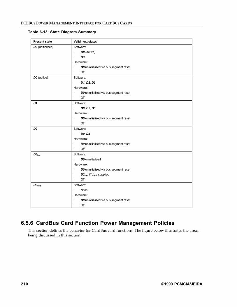
PCI BUS POWER MANAGEMENT INTERFACE FOR CARDBUS CARDS
210 ©1999 PCMCIA/JEIDA
Table 6-13: State Diagram Summary
Present state Valid next states
D0 (unitialized) Software:
á D0 (active)
á D3
Hardware:
á D0 uninitialized via bus segment reset
á Off
D0 (active) Software:
á D1, D2, D3
Hardware:
á D0 uninitialized via bus segment reset
á Off
D1 Software:
á D0, D2, D3
Hardware:
á D0 uninitialized via bus segment reset
á Off
D2 Software:
á D0, D3
Hardware:
á D0 uninitialized via bus segment reset
á Off
D3hot Software:
á D0 uninitialized
Hardware:
á D0 uninitialized via bus segment reset
á D3cold if VAUX supplied
á Off
D3cold Software:
á None
Hardware:
á D0 uninitialized via bus segment reset
á Off
6.5.6 CardBus Card Function Power Management PoliciesThis section defines the behavior for CardBus card functions. The figure below illustrates the areasbeing discussed in this section.

ELECTRICAL SPECIFICATION
© 1999 PCMCIA/JEIDA 211
PCI toCardBusBridge
Function
Config Regs
Function
SCOPE
Config Regs
CardBusCard
CardBusCard
Figure 6-8: Non-Bridge CardBus Function Power Management Diagram
The following tables define the behavior for a CardBus card function while operating in eachcombination of bus and functional power management states.
Legend:
CardBus Function PM State Current CardBus function power management state.
CardBus Bus PM State Current power management state of the CardBus functionÕs hosting CardBus bus segment.
Context Configuration register and functional state information that are required to be valid for thegiven power management state. The registers that must remain valid, and the features thatmust remain available for a given class of device are typically dictated by the correspondingDevice-class power management specification.
Power Power consumption
Access Delay The minimum required delay before attempting to access the CardBus function to change itspower state. If the bus is fully accessible (B0) then this delay is solely the result of the statetransition delay, or recovery time, following the last write to the functionÕs PowerState field. Ifthe bus is not in a fully accessible state (B1, B2 or B3) then the delay is characterized byeither the functionÕs state transition recovery time, or the time it takes to restore the bus to afully accessible state, whichever is greater.
Restore Time The total time from when a CardBus function transitions from its current power managementstate to the fully configured D0 active state. (Measurement beginning from either a write to thefunctionÕs PMCSR, or a bus segment reset).
Actions to Function Valid CardBus bus transactions that can be conducted with the function as the target of thetransaction.
Actions from Function Valid CardBus bus transactions, and/or operations that can be initiated by the function.

PCI BUS POWER MANAGEMENT INTERFACE FOR CARDBUS CARDS
212 ©1999 PCMCIA/JEIDA
Table 6-14: D0 CardBus Card Power Management Policies
CardBusBus PM
State
CardBusFunction PM
State
Context Power AccessDelay
RestoreTime
Actions toCardBus card
Actions from Function
B0 Legacy CardBusFunction (D0)
Full Full None None Any CardBusTransaction
Any CardBus Transactionor Interrupt
B0 D0(Uninitialized)
PMEContext*
<70mA Vcc: off -> on,245mA if transitioningfrom D3cold withPME_En true
None None CardBusConfig Cycles
None
B0 D0 (Active) Full Full None None Any CardBusTransaction
Any CardBus Transactionor Interrupt, PME*
B1-B3 D0 (Active) N/A** N/A** N/A** N/A** N/A** N/A**
Table 6-15: D1 CardBus Card Power Management Policies
CardBusBus PM
State
CardBusFunction PM
State
Context Power Access Delay RestoreTime
Actions toCardBus card
Actions from Function
B0 D1 Device ClassSpecific andPME Context*
< D0uninitialized
None DeviceClassSpecific
CardBusConfig Cycles
PME only*
B1 D1 Device ClassSpecific andPME Context*
< D0uninitialized
Busrestorationtime
DeviceClassSpecific
None PME only*
B2-B3 D1 N/A** N/A** N/A** N/A** N/A** N/A**
Table 6-16: D2 CardBus Card Power Management Policies
CardBusBus PM
State
CardBusFunction PM
State
Context Power Access Delay RestoreTime
Actions toCardBus card
Actions from Function
B0 D2 Device ClassSpecific andPME Context*
< next lowersupported PMstate, or < D0uninitialized
200 µs(Note 1)
DeviceClassSpecific
CardBusConfig Cycles
PME only*
B1 D2 Device ClassSpecific andPME Context*
< next lowersupported PMstate, or < D0uninitialized
Greater ofeither the busrestorationtime or 200 µs(Note 2)
DeviceClassSpecific
None PME only*
B2 D2 Device ClassSpecific andPME Context*
< next lowersupported PMstate, or < D0uninitialized
Greater ofeither the busrestorationtime or 200 µs(Note 2)
DeviceClassSpecific
none PME only*
B3 D2 N/A** N/A** N/A** N/A** N/A** N/A**

ELECTRICAL SPECIFICATION
© 1999 PCMCIA/JEIDA 213
Table 6-17: D3hot CardBus Card Power Management Policies
CardBusBusState
CardBusFunction PM
State
Context Power Access Delay RestoreTime
Actions toCardBus card
Actions from Function
B0 D3hot PME andfunctionalcontext*
< next lowersupported PMstate, or < D0uninitialized
10 ms(Note 1)
DeviceClassSpecific
CardBusConfig Cycles
PME only*
B1 D3hot PME andfunctionalcontext*
< next lowersupported PMstate, or < D0uninitialized
Greater ofeither the busrestorationtime or 10 ms(Note 2)
DeviceClassSpecific
none PME only*
B2 D3hot PME andfunctionalcontext*
< next lowersupported PMstate, or < D0uninitialized
Greater ofeither the busrestorationtime or 10 ms(Note 2)
DeviceClassSpecific
none PME only*
B3 D3hot PME andfunctionalcontext*
< next lowersupported PMstate, or < D0uninitialized
N/A N/A none PME only*
Table 6-18: D3cold CardBus Card Power Management Policies
CardBusBusState
CardBusFunction PM
State
Context Power Access Delay RestoreTime
Actions toCardBus card
Actions from Function
B3 D3cold PME contextonly*
VAUX N/A fullcontextrestore,or bootlatency
none PME only*
B3 Legacy CardBusFunction (D3)
none No Power N/A fullcontextrestore,or bootlatency
none none
Notes:* If PME is supported in this state** This combination of function and bus power management states is not allowed.*** Implies device specific, or slot specific power supplies which is outside the scope of this specification.Additional Notes:1. This condition is not typical. It specifies the case where the system software has programmed the
functionÕs PowerState field and then immediately decides to change its power state again. Typically thestate transition recovery time will have expired prior to a power state change request by software.
2. The more typical case where the bus must first be restored to B0 before being able access the functionresiding on the bus to request a change of its power state. State transition recovery time begins fromthe time of the last write to the functionÕs PowerState field. In this case the bus restoration time isdictated by state transition recovery times incurred in programming the busÕs originating device to D0which then transitions its bus to B0. Bus restoration time is typically the deciding factor in access delayfor this case. (see 6.5.6.1 State Transition Recovery Time Requirements)
When in D1, D2 or D3hot a CardBus function must not respond to CardBus transactions targeting itsI/O or memory spaces or assert a functional interrupt request.
A CardBus function cannot tell the state of its CardBus bus; therefore, it must always be ready toaccept a CardBus configuration access when in D1, D2 or D3hot.

PCI BUS POWER MANAGEMENT INTERFACE FOR CARDBUS CARDS
214 ©1999 PCMCIA/JEIDA
6.5.6.1 State Transition Recovery Time Requirements
The following table shows the minimum recovery times (delays) that must be guaranteed, byhardware in some cases and by system software in others, between the time that a function isprogrammed to change state and the time that the function is next accessed (including CardBusconfiguration space).
Table 6-19: CardBus Function State Transition Delays
Initial State Next State Minimum System Software Guaranteed Delays
D0 D1 0
D0 or D1 D2 200 µs
D0, D1 or D2 D3hot 10 ms
D1 D0 0
D2 D0 200 µs
D3hot D0 10 ms
6.6 CardBus Cards and Power ManagementWith power management under the direction of the operating system each class of devices (PCI andCardBus functions) must have a clearly defined criteria for feature availability as well as whatfunctional context must be preserved when operating in each of the power management states.Some example Device-Class specifications have been proposed as part of the Intel/Microsoft/ToshibaACPI Specification for various functions ranging from audio to network adapters. While definingDevice-Class specific behavioral policies for most functions is well outside of this specificationÕsscope, defining the required behavior for the CardBus interface function is within the scope of thisspecification. The definitions here apply to the PCI-to-CardBus cards.
The mechanisms for controlling the state of these function vary somewhat depending on which typeof originating device is present. The following sections describe how these mechanisms work forCardBus cards.
This section details the power management policies for CardBus card functions. The CardBus cardfunction can be characterized as a CardBus bus load.
The shaded regions in the figure below illustrate what will be discussed in this section.

ELECTRICAL SPECIFICATION
© 1999 PCMCIA/JEIDA 215
Config Regs
Function
Config Regs
Function
Config Regs
FunctionCardBus Segment
SCOPE
PCI
PCI toCardBus
Bridge
PCI Bus Segment
Figure 6-9: CardBus Card Power Management Diagram
The following table defines the relationship between a bridge functionÕs power management state,and that of its secondary bus. Also detailed are the resultant attributes of the secondary bus. Therightmost column of the table details a set of conditions that all "downstream" CardBus cardfunctions must be capable of withstanding when residing on a bus in a given state without theirapplication breaking in a way that cannot be gracefully recovered from.
It is the responsibility of the system software to ensure that only valid, workable combinations ofbus and downstream PCI-to-CardBus bridge and CardBus bus function power management statesare used for a given CardBus bus and the CardBus card functions residing on that bus.
Legend:
Bridge PM State Current CardBus function power management state of bridge function.
Secondary CardBus Bus State Current power management state of the originating deviceÕs CardBus bus segment.
Secondary CardBus Attributes The characteristics of the secondary bus for the current bus power management state.
Downstream Function Attributes Necessary attributes of a CardBus function residing on the secondary bus given thesecondary busÕs power management state.

PCI BUS POWER MANAGEMENT INTERFACE FOR CARDBUS CARDS
216 ©1999 PCMCIA/JEIDA
Table 6-20: CardBus Card Power Management Policies
Present state Valid next states CardBus Card Requirements in Present State
D0 (unitialized) Software:
á D0 (active)
á D3
Hardware:
á D0 uninitialized viaCardBus bus segmentreset
á Off
Vcc: On
Bus (including CCLK): Per PC Card Standard for appropriate card technology
Context (CardBus bus in B0)
PME_En false
No context, power on defaults
PME_En true
PME context
Power consumed by the CardBus card is < 70 mA if coming from no Vcc or VAUX, <245mA if PME_En true and returning from D3cold state
D0 (active) Software:
á D1
á D2
á D3
Hardware:
á D0 uninitialized viaPCI bus segment reset
á Off
Vcc: On
Bus (including CCLK): B0
CardBus clock is running unless Clock Run is asserted. If clock run is notfunctional in the PCI-to-CardBus bridge, clock is on
CardBus bus is fully functional
CardBus card functional and CardBusStatusChange interrupts are functional
All context, PCI and functional, is available.
Card responds appropriately to all CardBus bus cycles
Power consumed by the CardBus card is as specified by the vendor for the D0 / B0state
D1 Software:
á D0
á D2
á D3
Hardware:
á D0 uninitialized viaPCI bus segment reset
á Off
Vcc: On
Bus: B1
CardBus clock is running unless Clock Run is asserted. If clock run is notfunctional in the PCI-to-CardBus bridge, clock is on
CardBus bus is idle
CardBus card functional and CardBusStatusChange interrupts are not available
CardBus card PME# is available if PME_En is true
CardBus Card responsibilities:
All context, PCI and functional, is preserved; CardBus card PCI configurationspace is readable; functional context is not available; only CardBus card PowerManagement Control and Status Register PowerState bits are required to bewriteable
CardBus card only responds to CardBus type 0 cycles
Power consumed by the CardBus card is as specified by the vendor for the D1 / B1state but must be lower than the < 200mA
D2 Software:
á D0
á D3
Hardware:
á D0 uninitialized viaPCI bus segment reset
á Off
Vcc: On
Bus: B2
CardBus clock is not running unless Clock Run is required by CardBus card. Ifclock run is not functional in the PCI-to-CardBus bridge, clock is off
CardBus bus is idle
CardBus card functional and CardBusStatusChange interrupts are not available
CardBus card PME# is available if PME_En is true
CardBus card responsibilities:
All context, PCI and functional, is preserved; CardBus card PCI configurationspace is readable; functional context is not available
CardBus card only responds to CardBus type 0 cycles
Power consumed by the PCI-to-CardBus bridge is as specified by the vendorfor the D2 / B2 state but must be lower than the D1 / B1 state

ELECTRICAL SPECIFICATION
© 1999 PCMCIA/JEIDA 217
D3hot Software:
á D0 uninitialized
Hardware:
á D0 uninitialized viaPCI bus segment reset
á D3cold if VAUX supplied
á Off
Vcc: On
Bus: B3
CardBus clock is off
CardBus bus is indeterminate except CRST# and CCLK which must be low
Interrupts are not available
CardBus card PME# is available if PME_En is true
CardBus card responsibilities:
Only PME context is preserved if PME_En is true; CardBus card PCIconfiguration space is readable; functional PME context is not available; onlyCardBus card Power Management Control and Status Register PowerState,PME_En and PME_Status bits are required to be functional
CardBus card only responds to CardBus type 0 cycles
Power consumed by the PCI-to-CardBus bridge is as specified by the vendorfor the D3 / B3 state but must be lower than the D2 / B2 state
D3cold Software:
á None
Hardware:
á D0 uninitialized viaPCI bus segment reset
á Off
Vcc: Off, VAUX on if required
Bus: Off
CardBus clock is off
CardBus bus is indeterminate except CRST# and CCLK which must be low
Interrupts are not available
Card PME# is available if PME_En is true
CardBus card responsibilities:
Only PME context is preserved if PME_En is true
Does not respond to any PCI cycles
Power consumed by the CardBus card is required to be < 200 mA
6.6.1 CardBus Card ContextCardBus does not define a PME# signal, however it does define a signal with similar intendedusage. The Card Status Change signal will be used as a source for power management events for aCardBus card and /Status Change will be used for a PC Card. The PCI-to-CardBus Bridge will usethis event as one condition for assertion of PME#.
CardBus card CardBus PME context consists of the CardBus Function Event Register and theCardBus Function Event Mask Register.
6.6.2 PME_En/PME_Status and CardBus CardsA CardBus cardÕs PME_En has special requirements unlike a standard PCI device because there isno CardBus device driver defined in an ACPI operating system. In order to support powermanagement events using an ACPI operating systemÕs PCI device driver, the PME_En bit mustsupport generating a CSTSCHG for a CardBus card.
When the operating system sets PME_En true, this action must set (1) the GWAKE (bit 4) and WKUP(bit 14) bit fields in the CardBus Function Event Mask Register. Setting PME_En false must clear (0)GWAKE and WKUP as well. The CardBus function must continue to target the GWAKE bit in theFunction Event Register as the function general wakeup event. When enabled (PME_En true), aCSTSCHG event is latched into PME_Status and the CardBus cardÕs GWAKE bit in the FunctionEvent Register.
PME_En must make the CardBus card power management event functionality act as if the CardBuscard were a standard PCI device. PME_Status functionality maps to CardBusÕs CSTSCHG andPME_En functionality maps to CardBusÕs GWAKE / WKUP. Clearing the GWAKE / WKUP mask

PCI BUS POWER MANAGEMENT INTERFACE FOR CARDBUS CARDS
218 ©1999 PCMCIA/JEIDA
bits does not clear the PME_En bit in the PMCSR. If CSTSCHG is asserted, setting PME_En falsewill prevent the CSTSCHG pin from being asserted and clear the GWAKE and WKUP bits in theFunction Event Mask Register. Writing a "1" to the PME_Status bit will clear the GWAKE bit in theFunction Event Register and clearing the GWAKE bit in the Function Event Register clears thePME_Status bit in the PMCSR register.
Setting the Function Event Mask RegisterÕs READY (Ready/Busy), BVD1:2 (Battery Voltage detects)and WP (Write Protect) may also generate a CSTSCHG event, however, these bits are not requiredto track PME_En and BVD1, BVD2, READY and WP are not required to follow PME_Status. IfPME_En is false, changes in the CardBus card Function Event registers have no effect on PME_En /PME_Status.
It is imperative that each hardware configuration set be controlled by the appropriate softwarecontroller. It is expected that ACPI software configures power management in a CardBus card usingPME_En / PME_Status. Non-ACPI software should work with the CardBus Function Event registers.Furthermore, it is expected that a CardBus card configured through PME_En / PME_Status generatea PME# through the CardBusÕ bridge and a non-ACPI configured CardBus card generate aCSTSCHG through the CardBusÕ bridge.
Table 6-21: PME_En / PME_Status Summary in a CardBus Card
ACPI Operating System
CardBus PCIConfiguration
Space
Function Event Mask Register Function EventRegister
CardBus pin CardBus PCIConfiguration Space
PME_En GWAKE WKUP GWAKE CSTSCHG PME_Status
Default 0 Default 0 Default 0 Default 0 Default 0 Default 0
Written 1 Follows PME_En 0 0 0
1 1 1 0 0 0
1 1 1 1 1 Latches CSTSCHGchange
Written 0 Follows PME_En 1 0 1
DonÕt care DonÕt care DonÕt care 0 0 Written 1
Non-ACPI Operating System
No effect Per Electrical Specification No effect
The setting of the CardBus cardÕs PME_En enables the CSTSCHG signal to be active in states otherthan D0. Only if PME_En is true can the CardBus card assert CSTSCHG in device states D1, D2 andD3. CSTSCHG can be asserted with or without PME_En true in device state D0. If PME_En is true,then the assertion of CSTSCHG is latched into the CardBus cardÕs PCI Power ManagementPME_Status bit. There may be additional PME function context which must be preserved, but that isimplementation specific and is not addressed in this specification.
6.7 Power Management EventsThe Power Management Event (PME#) signal is defined as an open drain, active low signal that isto be driven low by a PCI function to request a change in its current power management stateand/or to indicate that a power management event has occurred. Since CardBus does not have a pinto dedicate to the PME# function, CardBusÕs CSTSCHG will implement the functionality. The leveland signal translation will be performed in the PCI-to-CardBus bridge.
. CardBus devices must be enabled by software before asserting this signal. Once asserted, thedevice must continue to drive the signal low until software explicitly clears the PME_Status or

ELECTRICAL SPECIFICATION
© 1999 PCMCIA/JEIDA 219
PME_En bit in the PMSCR register of the function. PME_STATUS and PME_En are only clearedwhen written with a "1".
PCI bus power management aware software will enable its use by setting the PME_En bit in thePMCSR. When a CardBus card function generates or detects an event which requires the system tochange its power state (e.g. the phone rings), the function will assert CSTSCHG. It must continue toassert CSTSCHG until software either clears the PME_En bit or clears the PME_Status bit in thePMCSR even if the source of the power management event is no longer valid (e.g. the phone stopsringing). This requirement is true even though the operating system software may clear the EventRegister bits which caused the PME. Some devices which are powered by a battery or some externalpower source may use this signal even when powered off. Such devices must maintain the value ofthe PME_Status bit through reset (CRST#).
6.7.1 Auxiliary Power for D3cold Power Management EventsPower managed systems that support PME generation while in the D3cold state may require anauxiliary power source. There are several ways to provide auxiliary power for any necessary "keepalive" circuitry including but not limited to:
1. On-Board Battery
2. AC "Brick" adapter, externally provided power source
3. Auxiliary power supplied by the system
In the case of the CardBus card, the auxiliary supply provided for the controller will be limited to200 mA provided via the Vcc pins as there are no pins available on the CardBus card connector thatcan be designated VAUX. The CardBus card must not consume more than 200 mA Icc when:
1. The CardBus card is programmed to the D3 state and
2. The CardBus clock is stopped and
3. The CardBus bus is idle and
4. The PME_Support bit 15, D3cold, bit is set
The transition from Vcc to VAUX can occur only after the above three conditions are implemented.Additionally, the transition from Vcc to VAUX must include the stable application of VAUX for aminimum of 50 ms prior to transitioning Vcc off. Likewise, when transitioning from off to on, VAUX
must remain stable for 50 ms after Vcc is up and stable. See Figure 6-10: Vcc to VAUX Transitioningfor more information.

PCI BUS POWER MANAGEMENT INTERFACE FOR CARDBUS CARDS
220 ©1999 PCMCIA/JEIDA
50ms
Vcc
CardBusgoinginactive
VAUX
Vcc transitions to VAUX
Figure 6-10: Vcc to VAUX Transitioning
6.8 Software Support for PCI Power ManagementThe PCI Power Management specification for CardBus defines the requirements for PCI andCardBus functions to be managed by an Operating System. The specification does not attempt todefine any sort of Power Management Policy. That is left up to the individual Operating System.However, it is necessary to address some of the basic assumptions that have been made regardingwhich aspects of power management are enforced by system software versus by hardware such thatthe functions might react appropriately. These assumptions fall into four basic categories:Identifying PCI and CardBus Function Capabilities, Placing PCI and CardBus Functions in a LowPower State, Restoring PCI and CardBus Functions from a Low Power State, and Wake Events.Within each of these areas, it has been assumed that the Operating System software will handlecertain power management functions in addition to itÕs basic power management policy. It must benoted that in the context of this chapter references to the Operating System software include anydevice drivers and other Operating System specific power management services.
6.8.1 Identifying CardBus Function CapabilitiesThe Operating System software is responsible for identifying all CardBus function powercapabilities by traversing the New Capabilities structure in CardBus cardÕs PCI Configuration space,and reading the Power Management Capabilities Register (PMC). It is the Operating SystemÕsresponsibility to ensure that it does not attempt to place a function into a power management statewhich the function does not support. If, for any reason, the Operating System software attempts toput a function into a power management state that the function does not support, the functionshould handle this gracefully31, and remain in whatever state it was in before the request. ThePowerState bits of the PMCSR will reflect the current state of the function, not the intended invalidstate which was written.
31 Finish the PCI transaction with normal completion and ignore the write data. This is NOT a hardware error
condition.

ELECTRICAL SPECIFICATION
© 1999 PCMCIA/JEIDA 221
6.8.2 Placing CardBus Functions in a Low Power StateWhen attempting to place a CardBus function in a low power state D1 - D3, it is the OperatingSystemÕs responsibility to ensure that the function has no pending (host initiated) transactions, or inthe case of a Bridge device, that there are no CardBus functions behind the bridge that require thebridge to be in the fully operational D0 state. Furthermore, it is the Operating SystemÕsresponsibility to notify any and all device drivers that are conducting peer-to-peer transfers to thetarget function that the target function will no longer be accessible. In other words, it is theOperating SystemÕs responsibility to ensure that no peer-to-peer activity occurs with the sleepingCardBus function as the target. If the Operating System and the PCI function both support WakeEvents, the Operating System should enable the functionÕs Power Management Event (PME# -CardBus cardÕs CSTSCHG) line via the PME_En bit in the functionÕs Power Management ControlRegister (PMCSR).
6.8.2.1 Buses
When attempting to place a CardBus Bus segment into a lower power management state (B1- B3)the Operating System must first ensure that all CardBus functions on that bus have been placed inan appropriate low power state.
6.8.2.2 D3 State
Prior to placing a CardBus function into D3, the Operating System must determine if it has thecapability to restore the function from this state. Restoration includes reinitializing the function. TheOperating System must make sure that it has the appropriate driver loaded for that function inorder to restore the functions to operation. If the Operating System is not capable of fullyreinitializing a device, then the Operating System should not put the device into D3. When placinga function into D3, the Operating System Software is required to disable I/O and memory space aswell as Bus Mastering via the CardBus PCI Command Register.
6.8.3 Restoring PCI Functions From a Low Power State
6.8.3.1 Dx States and the DSI Bit
For support of the DSI (Device Specific Initialization) bit, consult the PCI Bus Power ManagementSpecification.
6.8.3.2 D1 and D2 States
Restoring a function from D1 or D2 simply requires the Operating System to update the PowerStatefield of the PMCSR. System software must ensure that sufficient time elapses between when thePMCSR is updated and when the first access targeting that PCI function may occur.
6.8.3.3 D3 State
Restoring a function from D3 requires the Operating System to reinitialize the function, beginningwith, for the case of D3cold, restoring power to the device and initiating a PCI Bus Segment Reset.This is accomplished by either programming the hosting busÕs originating device to D0, or by otherACPI-type control methods. Full context must be restored to the function before it is capable ofresuming normal operation. For example reintialization includes, but is not necessarily limited torestoring the Base Address Registers, re-enabling the I/O and Memory spaces, re-enabling Bus
PCI BUS POWER MANAGEMENT INTERFACE FOR CARDBUS CARDS
222 ©1999 PCMCIA/JEIDA
Master capabilities, and unmasking any IRQs or PCI Interrupts as well as restoring the INT Lineregister. Furthermore, if the function has the DSI bit set, the Operating System is required toexecute whatever initialization code is necessary, either via the device driverÕs initialization code orexecuting POST.
6.8.4 Wake Events
6.8.4.1 Wake Event Support
PCI Power Management supports Wake events generated by functions on the PCI bus in which theCardBus cardÕs CSTSCHG becomes a PME# event. Assuming the Operating System supports WakeEvents, it is the system hardwareÕs responsibility to restore the Host processor subsystem to a statewhich will permit the Operating System to function (through ACPI or some other architecture). Ifthe sub-system is already in a D0 state, then the system hardware does not need to take any specialaction. The System is responsible for notifying the Operating System that a PCI Power ManagementEvent has occurred. It is expected that PME# will generate some form of System ConfigurationInterrupt (SCI), but whether this interrupt is handled by a device driver or an Operating Systemservice routine, is left up to the individual Operating System architecture.
Once the Operating System has been notified that a PCI PME has occurred, it is the OperatingSystemÕs responsibility to restore power to the primary PCI and CardBus bus and to restore it to theB0 state, then to restore power to any unpowered slots/devices, and finally query the PCI andCardBus functions that have been configured with PME# enabled to determine which function, orfunctions had generated PME#. If the generating device is a bridge device, the Operating Systemshould follow this procedure for any subsequent PCI bridges. Should PME# become deassertedbefore the Operating System identifies the device which generated it, or before the PME# isserviced, the Operating System must recover gracefully. Furthermore, the Operating System mustbe able to handle multiple PME#s generated by different functions simultaneously. Uponidentifying the source or sources of the PME#, it is up to the Operating System Power ManagementPolicy to identify the correct course of action with regard to waking the functions and/or the rest ofthe system.
6.8.4.2 The D0 "Initialized" State From a Wake Event
Before the Operating System returns a function to D0 which will require a re-initialization of thefunction, it must ensure that the Operating System not only has the information necessary to re-initialize the function, but also any information necessary to restore the function as well. Thisinformation is often client specific. As an example, assume a modemÕs client has set up a modemfunction in a specific state additional to default initialization (error correction, baud rate, modulationcharacteristics, etc.). The client/function then goes unused for an extended amount of time whichmay cause the power manager to place the modem in a D2 or perhaps even a D3 state.
When the client is called upon to interact with the modem (such as a ring-resume event), theOperating System will have transitioned the modem function to the D0 initialized state. Howeverrestoration of the modem function to D0 alone may not be sufficient for the function and client toperform the indicated task. It is manifest upon Device-Class specifications to include sufficientcontext save requirements for successful restoration of a function. The restoration must betransparent to the extent that the host application is unaware that a power state transition and theassociated restoration occurred.
Transitioning from D0 unitialized to D0 active is defined when the appropriate memory and IOwindows and busmastering enable bits are set by the operating system.

ELECTRICAL SPECIFICATION
© 1999 PCMCIA/JEIDA 223
6.8.5 Get CapabilitiesThe Get Capabilities operation is performed by the operating system as it is enumerating devices inthe system. Get Capabilities tells the Operating System information about what power managementfeatures the device supports. This includes which power states the device supports, whether or notthe device supports waking the machine and from what power states it is capable of wakeup.
6.8.6 Set Power StateThe Set Power State operation is used by the operating system to put a device into one of the fourpower states. The operating system will track the state of all devices in the system.
6.8.7 Get Power StatusThe Get Power Status operation is used by the operating system to determine the present state ofthe power configuration (power states & features). This operation will read the PMC and PMCSR toobtain this information. Software assumes that reported status information reflects the current state ofthe function. Therefore functions should update status information bits ONLY after carrying out theintended task.
6.9 Other ConsiderationsIn addition to supporting the minimum set of required mechanisms defined in this specification,designers of PCI devices and systems are encouraged to add additional power managementfunctionality, taking advantage of the optional headroom provided by this specification.
Designers are encouraged to design for low power consumption in all operating modes. The PCIMobile Design Guide makes several suggestions on designing for low power which are applicableto all devices. Even simple things such as minimizing current drain through pull-up resistors canadd up to real power savings.
Additional power saving techniques while in D0 are also encouraged as long as they aretransparent to the operating system.

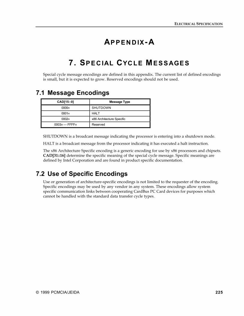
ELECTRICAL SPECIFICATION
© 1999 PCMCIA/JEIDA 225
A P P E N D I X - A
7 . S P E C I A L C Y C L E M E S S A G E S
Special cycle message encodings are defined in this appendix. The current list of defined encodingsis small, but it is expected to grow. Reserved encodings should not be used.
7.1 Message EncodingsCAD[15::0] Message Type
0000H SHUTDOWN
0001H HALT
0002H x86 Architecture Specific
0003H Ñ FFFFH Reserved
SHUTDOWN is a broadcast message indicating the processor is entering into a shutdown mode.
HALT is a broadcast message from the processor indicating it has executed a halt instruction.
The x86 Architecture Specific encoding is a generic encoding for use by x86 processors and chipsets.CAD[31::16] determine the specific meaning of the special cycle message. Specific meanings aredefined by Intel Corporation and are found in product specific documentation.
7.2 Use of Specific EncodingsUse or generation of architecture-specific encodings is not limited to the requester of the encoding.Specific encodings may be used by any vendor in any system. These encodings allow systemspecific communication links between cooperating CardBus PC Card devices for purposes whichcannot be handled with the standard data transfer cycle types.


ELECTRICAL SPECIFICATION
© 1999 PCMCIA/JEIDA 227
A P P E N D I X - B
8 . C A R D B U S P C C A R D C O N N E C T O R T E S T
M E T H O D O L O G Y
This appendix outlines a methodology which may be used to quantify the effect CardBus PC Cardand host connectors have on system noise levels. Connectors used for CardBus PC Cardimplementations shall provide sufficient signal ground return paths to support 33 MHz operation.The CardBus PC Card Electrical Specifications defines the criteria for 33 MHz operation, includingmaximum ground bounce noise for the interface.
8.1 BackgroundThere are many factors which contribute to overall signal quality and integrity across the CardBusPC Card interface, of which the CardBus PC Card connector is one of the most significant. Inaddition to the connector, several other factors may influence signal integrity across the interface.These include:
1. The quality of local and bulk decoupling on the host system and CardBus PC Card.
2. The output edge rate transmitted across the interface.
3. The frequency of operation.
4. The number of outputs switching simultaneously.
In order to understand the effect of any one variable in a system the effect of other variables mustbe minimized. The focus of this procedure is on the connector alone. This does not diminish theimportance of the other factors listed above, it just allows for a concise test procedure to bedocumented for the connector. This procedure or methodology, in conjunction with in-systemtesting, is intended to provide connector manufacturers with a standard for evaluation of theirproduct performance.
8.2 Test Hardware RecommendationsThis section defines the test hardware recommended for evaluation of the CardBus PC Cardconnector system. The CardBus PC Card connector system is comprised of a mated pair of CardBusPC Card connectors as specified by the Physical Specification. The test hardware for this systemincludes the connectors, mounting boards, interface circuitry and test/measurement equipmentnecessary to perform the evaluation. The test hardware should provide sufficient flexibility to meetthe recommendations defined in this appendix.
8.2.1 General Recommendations1. The test system should be on a stable platform and be capable of repeatable noise
measurements.
2. The design impedance of the boards should be matched to the CardBus PC Card drivers chosen,75 ohms is typical.
CARDBUS PC CARD CONNECTOR TEST METHODOLOGY
228 ©1999 PCMCIA/JEIDA
8.2.2 Host-side Requirements1. The power source should develop a clean VCC at voltages from 3.0 to 3.6 volts and have a
current rating of at least one ampere.
2. The test board should be capable of switching at least 45 outputs simultaneously into eachCardBus PC Card socket.
3. The test board should be capable of both driving and receiving signals.
4. It should be possible to measure ground bounce and VCC droop at all test points.
5. The output edge rate seen at the connector should be the maximum allowed by the CardBus PCCard specification.
6. It is recommended that series damping resistors be used to tune edge rates across the interface.
7. Either on or off board signal generation capable of 33 MHz speeds should be provided to drivethe CardBus PC Card interface I/O devices.
8. Test board construction and design should be consistent with current mobile computermethodology.
8.2.3 Card-side Recommendations1. The test board should be capable of driving or receiving at least 45 signals simultaneously.
2. It should be possible to measure ground bounce and VCC droop at all test points.
3. The output edge rate seen at the connector should be the maximum allowed by the CardBus PCCard specification.
4. It is recommended that series damping resistors be used to tune edge rates across the interface.
5. Either on or off board signal generation capable of 33 MHz speeds should be provided to drivethe CardBus PC Card interface I/O devices.
6. Test board construction and design should be consistent with current PC Card methodology.
7. The card boards should be capable of being stacked to accommodate 2 card vertical socketarrangements.
8.2.4 Measurement Equipment RecommendationsThe following test equipment considerations are recommended to support the test and measurementactivities:
Probe: Active FET probe 1.5 pF, 10X, 1 Megohm impedance
Probe GND: Less than 1" in length
Oscilloscope: HP54100 (or equivalent) Digitizing at 1 Gsample/S
8.3 Test Board ConsiderationsThis section provides block diagram layouts for both test boards and identifies the major attributesof each. The board layouts and features of each are provided as examples of a functional test setup.Individual adaptations and variations are acceptable as long as the results produced are comparableto those achievable with the described setup.

ELECTRICAL SPECIFICATION
© 1999 PCMCIA/JEIDA 229
8.3.1 Host-side ImplementationThe following features are descriptive of the test board used for the host side of the test setup(reference Figure B-1: Host-side Test Board Layout):
• Surface mount series resistance on all signal lines.
• Utilizes HP8180, or equivalent, word generator to drive I/O devices.
• Test points designed to accommodate 1 GHz FET probe.
• Maximum capacitive decoupling provided at the connector, the power source, and for everydevice.
• Matched trace lengths for simultaneous switching experimentation.
• Utilizes 16245, or equivalent, I/O drivers (24 mA output drive)
• Word wide control over OE# signals, allows for varied number of outputs switching.
• No vias between device pins and connector pins to maintain trace impedances which aredesigned for 75 ohms.
• Corner mounting holes provide for sturdy platform mounting.
• Three (3) pin headers allow for static high or low noise measurements at each test point.
• Crosstalk measurement points may be terminated or unterminated.
• Eight (8) 16245, or equivalent, devices allow for greater than 45 outputs switching into eachsocket at the same time.
CardBus PC Card
Connector
POWER SUPPLY
GROUND BOUNCEMEASUREMENT
GROUND BOUNCEMEASUREMENT
GROUND BOUNCEMEASUREMENT
SERIES RESISTOR TERMINATION– AS REQUIRED
I/O DRIVERDATA INPUT
I/O DRIVERDATA MONITOR
I/O DRIVERTRANSMIT/RECEIVE
CARD 0 AND 1
I/O DRIVERGROUND BOUNCE
CONTROL
I/O DRIVERS
I/O DRIVERS
Figure 8Ð1 Host-side Test Board Layout

CARDBUS PC CARD CONNECTOR TEST METHODOLOGY
230 ©1999 PCMCIA/JEIDA
8.3.2 Card-side ImplementationThe following features are descriptive of the test board used for the card side of the test setup (SeeFigure 8Ð2 Card-side Test Board Layout.):
• Surface mount series resistance on all signal lines.
• Utilizes HP8180 or equivalent word generator to drive I/O devices.
• Test points designed to accommodate 1 GHz FET probe.
• Maximum capacitive decoupling provided at the connector and for every device.
• Matched trace lengths for simultaneous switching experimentation.
• Utilizes TI VHC245, or equivalent, I/O drivers (8 mA output drive)
• Byte-wide control over OE# signals, allows for varied number of outputs switching.
• No vias between device pins and connector pins to maintain trace impedances. which aredesigned for 75 ohms
• Corner mounting holes provide for sturdy platform mount and board stacking capability.
• Three (3) pin headers allow for static high or low noise measurements at each test point.
• Crosstalk measurement points may be terminated or unterminated.
• Eight (8) TI VHC245, or equivalent, devices allow for greater than 45 outputs switching.
CardBus PC Card
Connector
GROUND BOUNCEMEASUREMENT
GROUND BOUNCEMEASUREMENT
GROUND BOUNCEMEASUREMENT
SERIES RESISTOR TERMINATION– AS REQUIRED
I/O DRIVERDATA INPUT
I/O DRIVERDATA MONITOR
I/O DRIVERTRANSMIT/RECEIVE
CARD 0 AND 1
I/O DRIVERGROUND BOUNCE
CONTROL
I/O DRIVERS
I/O DRIVERS
Figure 8Ð2 Card-side Test Board Layout

ELECTRICAL SPECIFICATION
© 1999 PCMCIA/JEIDA 231
8.4 Measurement MethodologyThe ground bounce measurements should always be taken in reference to the "local" ground. This"local" reference gives an accurate picture of what the receiving devices will "see" and respond to ina system. In a two card vertically mounted host system, four singular Card-Host driver-receiverpairings are possible, as follows:
Driver Receiver
Host Card 0
Host Card 1
Card 0 Host
Card 1 Host
8.4.1 Finding the Worst Case Ground BounceThe technique for finding a "worst case" is simply to try all available alternatives and use themeasurement point that provides the highest ground bounce measurement. The most importantaspect of this is in the design of the test system itself. The test system should provide multipleground bounce test points positioned as far away as possible from connector power and groundpins.
Host Conditions: Card conditions:
VCC = 3.6 V VCC = 3.6 V
Frequency = 1 MHz Frequency = 1 MHz
To find worst case ground bounce, all driver devices should be enabled. Then the data timing isadjusted so all outputs are actively switching simultaneously at frequency. In this configuration, thetest system is supporting at least 45 outputs switching across the CardBus PC Card interface. Groundbounce data may then be taken at each test point.
This technique may then be applied to each of the four singular combinations above. A true worstcase may be found by applying the two worst singular conditions for Cards 0 and 1 simultaneouslyacross the vertical CardBus PC Card connector and measuring as before. Now that the worst casemeasurement point has been located, the frequency may be ramped to 33 MHz and the groundbounce monitored to ensure proper operation to the maximum CardBus PC Card system frequency.


ELECTRICAL SPECIFICATION
© 1999 PCMCIA/JEIDA 233
A P P E N D I X - C
9 . P C C A R D C U S T O M I N T E R F A C E S
9.1 Custom Interface RequirementsThe features and capabilities of specific custom interfaces are described in this appendix. (See also4.3.5 Custom Interfaces.) This section, 9.1 and its subordinates, list the headings and describe thecontents of each paragraph required.
The title of paragraph 9.x, where x is two (2) and above, is the name for the custom interfacefollowed by the custom interface identification number in parenthesis. For example, Ò9.2 ZV Port(0141H).Ó
9.1.1 Purpose/OverviewDescribe the custom interface giving the primary purpose and an operational overview of theinterface.
9.1.2 CompatibilityThe addition of support for a custom interface does not relax any requirement in both the host andthe card associated with 16-bit PC Cards or CardBus PC Cards. PC Cards not using a custominterface shall not be adversely affected by the presence or state of a custom interface capabilityanywhere in the host.
Describe signals not available to cards using the custom interface while the custom interface isenabled. For example, a custom interface that redefines the SPKR# signal does not allow a PC Cardto use the optional 16-bit PC Card Binary Audio signal.
9.1.3 Pin AssignmentsDescribe all pin assignments.
9.1.4 FeaturesDescribe the features of the custom interface. As an example: ÒThis interface supports random accessto 16 Bytes of memory address per memory space using signals A[3::0].Ó
9.1.5 Signal DescriptionDescribe each signal as used while the custom interface is active. Identify each custom interfacesignal under one of four classifications: I (Input), O (Output), I/O (Bi-directional), and R (Reserved).Input signals are driven by the host and output signals are driven by the card.

PC CARD CUSTOM INTERFACES
234 ©1999 PCMCIA/JEIDA
9.1.6 FunctionsDescribe the functions for any and all address spaces available while the custom interface is active.
9.1.7 TimingDescribe the access timing for any and all address spaces available while the custom interface isactive.
9.1.8 Electrical InterfaceIdentify the characteristics of the electrical interface while the custom interface is active. Include logiclevels and address decoding mechanisms in describing the electrical interface.
9.1.9 Specific Signals and FunctionsProvide further discussion, as needed, of specific signals and functions available while the custominterface is active.

ELECTRICAL SPECIFICATION
© 1999 PCMCIA/JEIDA 235
9.2 ZV Port Custom Interface (0141H)The ZV Port is a single-source uni-directional video bus between a PC Card socket and a VGAcontroller. The ZV Port complies with CCIR601 timing to allow NTSC decoders to deliver real-timedigital video straight into the VGA frame buffer from a PC Card. The ZV Port also uses an industrystandard mechanism for transferring digital audio PCM data to a low cost DAC for conversion to ananalog signal.
9.2.1 OverviewThe following diagram shows the system level concept of the ZV Port. The diagram demonstrateshow TV in a window could be achieved in a portable computer with a low cost PC Card. An MPEG,or a teleconferencing card could also be plugged into the PC Card slot.
PCILocal Bus
PC CardHost
Adapter
VGA
ZV Port(Video)
256Kx16DRAM
19
AudioCodec PC Card Slot
NTSC/PALRF Signal
PC Card
VideoDecoder
Video
PC CardInterface
4
AudioPCMConverter
Amp
4
LCD CRTTV
SPEAKERS
AnalogEncoder
Motherboard
PCMAudioInput
19
Video & Control
Audio
Figure 9-1 Example ZV Port Implementation
9.2.2 CompatibilityThe addition of support for the ZV Port interface does not relax any requirement associated with 16-bit PC Cards or CardBus PC Cards in either the host or the card. PC Cards not using the ZV Portinterface shall be unaffected by the presence or state of the ZV Port interface capability anywhere inthe host.
PC Cards implementing the ZV Port interface shall present the 16-Bit PC Card memory onlyinterface following the application of VCC or the RESET signal. When either the 16-Bit PC Cardmemory only interface or the ZV Port interface is active the card shall support direct access to 16
PC CARD CUSTOM INTERFACES
236 ©1999 PCMCIA/JEIDA
Bytes (signals A[3::0]) of attribute and common memory space and provide access to two 64 Mbyteindirect memory spaces using registers in common memory. (See 4.16 Indirect Access to PC CardMemory.) Direct access to any address beyond the first 16 Bytes of attribute or common memory isundefined.
16-bit PC Card DMA operation shall not be supported in a socket when the ZV Port interface isactive because the entire set of pins over which the DREQ# signal can be routed, SPKR#,INPACK# or IOIS16#, are in use.
The I/O Is 16 Bit Port (IOIS16#) signal is not available when the ZV Port interface is active. PCCards supporting I/O operations while using the ZV Port interface shall indicate eight or 16 bit I/Oaccess via the TPCE_IO field in the CISTPL_CFTABLE_ENTRY tuple.
The Input Port Acknowledge (INPACK#) signal is not available when the ZV Port interface isactive.
The Audio Digital Waveform (SPKR#) signal is not available when the ZV Port interface is active;digital audio PCM is provided. (See 9.1.9 Specific Signals and Functions.)The Battery Voltage Detect2 (BVD2) signal may be available in the cardÕs Pin Replacement register while the ZV Portinterface is active. (See 4.15.3 Pin Replacement Register.)

ELECTRICAL SPECIFICATION
© 1999 PCMCIA/JEIDA 237
9.2.3 Pin AssignmentsThe following table shows the function of various PC Card signals when the ZV Port custominterface mode is set in the PC Card Host Adapter. PC Card signals not mentioned in the tablebelow, remain unchanged from the 16-bit PC Card I/O and Memory interface.
Table 9-1 ZV Port Interface Pin Assignments
PC CardPin
Number
I/O and MemoryInterface Signal
Name
I/O andMemory
I/O 1
ZV PortInterface Signal
Name
ZV PortI/O 1
Comments
8 A10 I HREF O Horizontal Sync to ZV Port
10 A11 I VSYNC O Vertical Sync to ZV Port
11 A9 I Y0 O Video Data to ZV Port YUV:4:2:2 format
12 A8 I Y2 O Video Data to ZV Port YUV:4:2:2 format
13 A13 I Y4 O Video Data to ZV Port YUV:4:2:2 format
14 A14 I Y6 O Video Data to ZV Port YUV:4:2:2 format
19 A16 I UV2 O Video Data to ZV Port YUV:4:2:2 format
20 A15 I UV4 O Video Data to ZV Port YUV:4:2:2 format
21 A12 I UV6 O Video Data to ZV Port YUV:4:2:2 format
22 A7 I SCLK O Audio SCLK PCM Signal
23 A6 I MCLK O Audio MCLK PCM Signal
24::25 A[5::4] I RESERVED RFU Put in three state by Host AdapterNo connection in PC Card
26::29 A[3::0] I ADDRESS[3::0] I Used for accessing PC Card
33 IOIS16# O PCLK O Pixel Clock to ZV Port
46 A17 I Y1 O Video Data to ZV Port YUV:4:2:2 format
47 A18 I Y3 O Video Data to ZV Port YUV:4:2:2 format
48 A19 I Y5 O Video Data to ZV Port YUV:4:2:2 format
49 A20 I Y7 O Video Data to ZV Port YUV:4:2:2 format
50 A21 I UV0 O Video Data to ZV Port YUV:4:2:2 format
53 A22 I UV1 O Video Data to ZV Port YUV:4:2:2 format
54 A23 I UV3 O Video Data to ZV Port YUV:4:2:2 format
55 A24 I UV5 O Video Data to ZV Port YUV:4:2:2 format
56 A25 I UV7 O Video Data to ZV Port YUV:4:2:2 format
60 INPACK# O LRCLK O Audio LRCLK PCM signal
62 SPKR# O SDATA O Audio PCM Data signal
1. "I" indicates signal is input to PC Card, "O" indicates signal is output from PC Card.
After HREF has started, the transfer of UV data always starts with the U component.UV[7::0] starts with U[7::0] at the first pixel of the line, then V[7::0], then U[7::0], É

PC CARD CUSTOM INTERFACES
238 ©1999 PCMCIA/JEIDA
The following diagram shows the PC Card socket and the location of the signals that carryvideo/audio signals when the PC Card and the Host Adapter are in ZV Port mode. This diagramshows the rationale behind selecting these signals to maintain signal integrity and minimize noise.
12
3536
GND GND
HREF
VSYNC
Y0Y2
Y3
Y1
Y5
Y4
Y6
Y7UV0
VPP
VCC
VPP
VCC
UV2
UV4
UV1UV3
UV7UV5UV6
Reserved
INPACK# (LRCLK)
SPKR# (SDATA)
A3
A2A1
A0
33PCLK
34
GND GND
6867
A6
A7
(MCLK)
(SCLK)
Figure 9-2 ZV Port Signals on PC Card Socket

ELECTRICAL SPECIFICATION
© 1999 PCMCIA/JEIDA 239
9.2.4 FeaturesIn the ZV Port interface mode, most of the host adapter control signals and data bus follow the samedata path to the card as it would for any other 16-bit PC Card in I/O and Memory mode. Theprimary difference is that the address signals A[25::4] are put in three state by the PC Card HostAdapter thereby restricting the Common Memory space address range to sixteen bytes and theAttribute Memory space address range to eight valid bytes. The unused address pins are used todefine the 19 pin ZV Port data bus, control signals, and 4 wire digital audio interface.
Because ZV Port restricts PC Card memory access to four address lines, A[3::0], cards implementingthe ZV Port interface will also implement indirect memory access. (See 4.16 Indirect Memory Accessand see also the Metaformat Specification.)
9.2.5 Signal DescriptionThis section describes the signal definitions of ZV Port. When the ZV Port custom interface isselected in the PC Card Host Adapter, address lines A[25::4] to the PC Card are either put in threestate by the Host Adapter or become inputs to the Host Adapter. The address lines A[25::4],BVD2/SPKR# and INPACK# signals are then replaced by ZV Port signals which carryvideo/audio data from the PC Card to the ZV Port.
The ZV Port interface has the following unique signals detailed in the sections below.
9.2.5.1 PCLK
This signal is used to clock valid data and HREF signal into the ZV Port. The maximum rate is 16MHz. During display time, rising edge of PCLK is used to clock the 16-bit pixel data into the ZVPort.
9.2.5.2 VSYNC
This signal supplies the vertical synchronization pulse to the ZV Port that displays the video data.
9.2.5.3 HREF
This signal supplies the horizontal synchronization pulse to the ZV Port that displays the videodata.
9.2.5.4 Y[7::0]
These signals are 8 bits of luminance data that are input to the ZV Port from the PC Card.
9.2.5.5 UV[7::0]
These signals are the 8 bits of chrominance data that are input to the ZV Port from the PC Card.
9.2.5.6 LRCLK
This signal determines which audio channel (left/right) is currently being input on the audio SerialData input line. LRCLK is low to indicate the left channel and high to indicate the right channel.Supported sample frequencies are shown in section 9.2.5.9 MCLK. For an MCLK frequency of 384Fsthe LRCLK to SCLK ration must be 48. For an MCLK frequency of 256Fs the LRCLK to SCLK rationmust be 32.

PC CARD CUSTOM INTERFACES
240 ©1999 PCMCIA/JEIDA
9.2.5.7 SDATA
This signal is the digital PCM signal that carries the audio information. Digital audio data istransferred using the I2S format.
I2S FormatThe I2S formats are shown below. The digital audio data is left channel-MSB justified to the high-to-low going edge of the LRCLK plus one SCLK delay.
LRCLK Left Channel Right Channel
SCLK
6 5 4 3 2 1 09 8 715 14 13 12 11 10 6 5 4 3 2 1 09 8 715 14 13 12 11 10SDATA
Figure 9-3: 1A I2S Format - MCLK = 256fs
LRCLK Left Channel Right Channel
SCLK
6 5 4 3 2 1 018 17 723 22 21 20 19SDATA 16 15 14 1312 11 10 9 8 6 5 4 3 2 1 018 17 723 22 21 20 19 16 15 14 1312 11 10 9 8
Figure 9-4: 1B I2S Format - MCLK = 384fs
9.2.5.8 SCLK
This signal is the serial digital audio PCM clock.
9.2.5.9 MCLK
This signal is the Master clock for the digital audio. MCLK is asynchronous to LRCLK, SDATAand SCLK.
The MCLK must be either 256x or 384x the desired Input Word Rate (IWR). IWR is the frequency atwhich words for each channel are input to the DAC and is equal to the LRCLK frequency. Thefollowing table illustrates several standard audio word rates and the required MCLK and LRCLKfrequencies.
The ZV Port audio DAC should support a MCLK frequency of 256 times and 384 times the inputword rate. This results in the frequencies shown below.
LRCLK (Hz)Sample Frequency
SCLK (MHz)32xfs
MCLK (MHz)256x
22050 0.7056 5.6448
32000 1.0240 8.1920
44100 1.4112 11.2896
48000 1.5360 12.2880

ELECTRICAL SPECIFICATION
© 1999 PCMCIA/JEIDA 241
LRCLK (Hz)Sample Frequency
SCLK (MHz)48xfs
MCLK (MHz)384x
22050 1.0584 8.4672
32000 1.5360 12.2880
44100 2.1168 16.9344
48000 2.3040 18.4320
9.2.6 FunctionsThere are no changes to the functions of the Common Memory and Attribute Memory areas whenthe ZV Port custom interface mode is set in the PC Card Host Adapter. (See 4.6 Memory Function.)The PC Card shall support direct access to 16 Bytes (signals A[3::0]) of attribute and commonmemory space and provide access to two 64 Mbyte indirect memory spaces using registers incommon memory. (See 4.16 Indirect Access to PC Card Memory.) Direct access to any addressbeyond the first 16 Bytes of attribute or common memory is undefined.
DMA Signals shall not replace I/O Interface Signals on a socket when the ZV Port custom interfacemode is set in the PC Card Host Adapter for that socket.
9.2.7 Timing
9.2.7.1 Video Interface Timing
The following timing diagram depicts the relationship amongst the ZV Port signals. The associatedvideo interface timing table shows the AC parameters associated with the ZV Port signals when theZV Port custom interface is in use.
VSYNC
HREF
PCLK
Y[7:0] / UV[7:0]
Even Field Odd Field
t5
t3
t2
t1
t4
t6
t7
1 20 END3
t6
t8
t8
t7
Figure 9-5 Video Interface Timing

PC CARD CUSTOM INTERFACES
242 ©1999 PCMCIA/JEIDA
Table 9-2 AC Parameters for Video Signals
Symbol Parameter Minimum Maximum
t1 PCLK fall time 4 ns 8 ns
t2 PCLK low time 20 ns
t3 PCLK rise time 4 ns 8 ns
t4 PCLK high time 20 ns
t5 PCLK cycle time 62.5 ns
t6 Y[7::0] / UV[7::0] / HREF setup time 30 ns
t7 Y[7::0] / UV[7::0] / HREF hold time 10 ns
t8 VSYNC setup / hold time to HREF 100 ns
Note: All video signals have a minimum rise and fall time of 4 ns and a maximum rise and fall time of 8 ns.Non-interlaced data asserts VSYNC at the Odd Field timing.
9.2.7.2 Audio Interface Timing
LRCLK
SCLK
SDATA
tslrd
tslrs
tsclkl
tsclkh
tsdhtsdlrs
Figure 9-6 Audio Interface Timing
Table 9-3 AC Parameters for Audio Signals
SYMBOL PARAMETER MIN
tslrd LRCLK delay 2ns
tslrs LRCLK setup 32ns
tsclkl bit clock low 22ns
tsclkh bit clock high 22ns
tsdlrs data setup 32ns
tsdh data hold 2ns
9.2.8 Electrical InterfacePC Card logic levels are unchanged when the ZV Port custom interface mode is set in the PC CardHost Adapter. (See 4.9.1 Signal Interface and Table 4-18 PC Card Logic Levels.)

ELECTRICAL SPECIFICATION
© 1999 PCMCIA/JEIDA 243
Table 9-4 ZV Port Electrical Interface
Item Signal Card Host
ZV Port Signals PCLKVSYNCHREFY[7::0]UV[7::0]LRCLKSDATASCLKMCLK
The card shall be able to drive aload of 50 pF at a DC current of 4mA in the low state and 700 µA inthe high state.
The host shall presenta load of no more than50 pF at a DC currentof 4 mA in the low stateand 700 µA in the highstate.
9.2.9 Specific Signals and FunctionsThe specific signals and functions of the ZV Port interface are discussed in the previous sections.
9.2.10 PC Card Connector Test MethodologyThis section notes changes in test methodology that should be observed when quantifying the effectof a ZV Port interface on system noise levels in a CardBus capable host. (See Appendix B: 8.CardBus PC Card Connector Test Methodology.)
The testing methods outlined in the appendix are the same, the test conditions are different. Inaddition to testing with the forty-five (45) CardBus signals that operate at 3.0 to 3.6 volts and afrequency of 33 MHz, the forty-five (45) ZV signals are added to the Host-side and Card-side testrequirements. The ZV Port interface also operates at 5 volts in addition to the 3.3 volt signalingenvironment used in CardBus and ZV has twenty-three (23) signals at 16.6 MHz and twenty-two(22) signals at 5.5 MHz.
Worst case ground bounce evaluation is expanded to include the ZV Port interface active atmaximum VCC (5.25 volts) and interactions with the forty-five (45) ZV signals.
The ZV Port interface in a CardBus PC Card capable host may be implemented using stubbedsignal traces when the stubs are short avoiding transmission line effects; any stub shall have amaximum length of 2 inches (50.8 mm). (See Figure 9-7 Host-side Test Board Layout.) Note that astubbed implementation allows vias between device pins and connector pins.

PC CARD CUSTOM INTERFACES
244 ©1999 PCMCIA/JEIDA
STACKEDCARDBUS
CONNECTOR
MIXED VOLTAGEPOWER SUPPLY
GROUND BOUNCEMEASUREMENT
GROUND BOUNCEMEASUREMENT
GROUND BOUNCEMEASUREMENT
SERIES RESISTOR TERMINATION– AS REQUIRED
I/O DRIVERDATA INPUT
I/O DRIVERDATA MONITOR
I/O DRIVERTRANSMIT/RECEIVE
CARD 0 AND 1
I/O DRIVERGROUND BOUNCE
CONTROL
I/O DRIVERS
I/O DRIVERS
INPUT BUFFER
I/O DRIVERS
Figure 9-7 Host-side Test Board Layout

ELECTRICAL SPECIFICATION
© 1999 PCMCIA/JEIDA 245
9.3 DVB CI Port Custom Interface (0241h)The DVB CI port is a bi-directional video and audio bus and a command control interface based onthe PC Card socket providing a DVB (Digital Video Broadcasting, European TV Standardizationbody) compliant Conditional Access System built into a PC Card or a PC Card adapter module. Themodule complements an IRD host system (Integrated Receiver Decoder) for receiving digitalencoded and scrambled TV applications. The Port complies with the specifications of EN 50221(CENELEC) laid out for timing of the interface to allow DVB compliant decoders to daisy chainscrambled data and to deliver unscrambled real-time MPEG-2 transport data streams straight intothe de-multiplexing and MPEG decoding process of the IRD.

PC CARD CUSTOM INTERFACES
246 ©1999 PCMCIA/JEIDA
9.3.1 OverviewThe IRD receiver for Digital Video Broadcasting services receives a digital data multiplex,structured according to the MPEG-2 specifications. Digital video data are received from a satellitetransponder, a cable system, from terrestrial transmitters or from telecommunications network.
After error correction this multiplex is fed via a descrambler, to recover scrambled services, to a de-multiplexer where the desired services - video, audio and data - are extracted and fed to theappropriate host decoder referred to as 'host' because of the variety of possible platforms which mayperform these operations. In the model of this process the descrambler and its associated controlfunctionality reside on a PC Card module which communicates with the host by means of the DVBCommon Interface which is defined on the PC Card physical layer as the DVB CI Port. Thefollowing block diagrams shows the system level concept of the DVB CI Port integrated into an IRDhost environment and demonstrate how a DVB Conditional Access is operated in principal forreceiving data streams.
Tuner Demodulator MPEG Decoder
DemultiplexerMicroprocessorRemote
Microprocessor
Host
Descrambler
ScrambledTransport Stream
DescrambledTransport Stream
Common Interface
RGB Out
Audio Out
RF In
Verifier
Control
Module
Verifier
SmartCard
(Optional)
Figure 9-8: Example DVB CI Port Implementation
Two logical interfaces, to be included on the same physical interface, are defined. The first interfaceis the MPEG-2 Transport Stream. The link and physical layers are defined in the Common Interfacespecification of EN 50221 and the higher layers are defined by MPEG. The second interface, thecommand interface, carries commands and data between the host and the module. Six layers aredefined in the Common Interface specification for this interface.
Note that a host can support more than one instance of this interface. In this case the MPEG-2Transport Stream interface is daisy-chained through all DVB CI sockets, as shown in Figure 9-9, andeach command interface is a separate logical connection to the host.

ELECTRICAL SPECIFICATION
© 1999 PCMCIA/JEIDA 247
HostCA module 1
CA module 2
CA module n
Figure 9-9: Transport Stream Interface Chaining between Modules
9.3.2 CompatibilityThe addition of support for the DVB CI Port interface does not relax any requirement associated with16-bit PC Cards or CardBus PC Cards in either the host or the card. However in case the host is notcapable of operating with PC Cards in a non-custom interface mode the card shall be gracefullyrejected by the host. PC Cards not using the DVB CI Port interface shall be unaffected by thepresence or state of the DVB CI Port interface capability anywhere in the host.
PC Cards implementing the DVB CI Port interface shall present the 16-bit PC Card memory onlyinterface following the application of VCC or the RESET signal. When either the 16-bit PC Cardmemory only interface or the DVB CI Port interface is active the card shall support direct access to 8kBytes (signals A[13::0]) of attribute memory. Access to any address beyond the first 8 kBytes ofattribute or common memory is possible by indirect addressing.
When operating in this configuration D[7::0] are retained as a byte-oriented I/O port, and thecapability to read the Attribute Memory is retained.
In DVB Common Interface Specification only two address lines are required for four Bytes of registerspace, but address lines A[13::0] are available to address Attribute Memory, if required. IOIS16# isnever asserted and the module ignores CE2#.
The Audio Digital Waveform (SPKR#) and the Status Changed (STSCHG#) signals are notavailable when the DVB CI Port custom interface mode is active. BVD1 and BVD2 shall remainÓhighÓ, the CE2# signal shall be ignored and interpreted by the module as always being in theÓhighÓ state. The IOIS16# signal is never asserted.

PC CARD CUSTOM INTERFACES
248 ©1999 PCMCIA/JEIDA
9.3.3 Pin AssignmentsThe following table shows the function of various PC Card signals when the DVB CI Port custominterface mode is set in the PC Card Host Adapter. PC Card signals not mentioned in the tablebelow, remain unchanged from the 16-bit PC Card I/O and Memory interface.
Table 9-5: DVB CI Port Interface Pin Assignments
PC CardPin
Number
I/O and MemoryInterface Signal Name
I/O andMemory
I/O1
DVB CI PortInterface Signal
Name
DVB CI PortI/O1
Comments
56 A25 I MDI7 I MPEG Data In 7
55 A24 I MDI6 I MPEG Data In 6
54 A23 I MDI5 I MPEG Data In 5
53 A22 I MDI4 I MPEG Data In 4
50 A21 I MDI3 I MPEG Data In 3
49 A20 I MDI2 I MPEG Data In 2
48 A19 I MDI1 I MPEG Data In 1
47 A18 I MDI0 I MPEG Data In 0
46 A17 I MISTRT I MPEG Data In Start
19 A16 I MIVAL I MPEG Data In Valid
20 A15 I MCLKI I MPEG Data Clock Input
14 A14 I MCLKO O MPEG Data Clock Output
41 D15 I/O MDO7 O MPEG Data Out 7
40 D14 I/O MDO6 O MPEG Data Out 6
39 D13 I/O MDO5 O MPEG Data Out 5
38 D12 I/O MDO4 O MPEG Data Out 4
37 D11 I/O MDO3 O MPEG Data Out 3
66 D10 I/O MDO2 O MPEG Data Out 2
65 D9 I/O MDO1 O MPEG Data Out 1
64 D8 I/O MDO0 O MPEG Data Out 0
63 BVD1 O MOSTRT O MPEG Data Out Start
62 BVD2 O MOVAL O MPEG Data Out Valid
1. "I" indicates signal is input to PC Card, "O" indicates signal is output from PC Card.

ELECTRICAL SPECIFICATION
© 1999 PCMCIA/JEIDA 249
The following diagram shows the PC Card socket and the location of the signals that carry digitalvideo-audio I/O-signals when the PC Card and the Host Adapter are set to the DVB CI Port custominterface mode.
12
3536
GND GND
MDO7
MISTRT
MDO6MDO5
MDI0
MDO4
MDI1
MDO3
MDO2
MDI2MDI3
VPP
VCC
VPP
VCC
MIVAL
MCLKI
MDI4
MDI5
MDI7MDI6
MDO1
SPKR# (MOVAL)
MOSTRT
33PCLK
34
GND GND
6867
MDO0
MCLKO
Figure 9-10: DVB CI Port Signals on PC Card Socket
9.3.4 FeaturesIn the DVB CI Port custom interface mode, most of the host adapter control signals and data busfollow the same signal path to the card as they would for any other 16-bit PC Card in I/O andMemory mode. The primary difference is that the address signals A[25::14] and the data signalsD[15::8] are used by the PC Card Host Adapter thereby restricting the Common Memory space(optional) address range to 16 kBytes and the Attribute Memory space address range to 8k validBytes (8 bit even access only).

PC CARD CUSTOM INTERFACES
250 ©1999 PCMCIA/JEIDA
9.3.5 Signal DescriptionThis section describes the signal definitions of DVB CI Port. When the DVB CI Port custom interfacemode is selected in the PC Card Host Adapter, address lines A[25::14] to the PC Card are put inhigh impedance state by the Host Adapter. The address lines A[25::14], the data lines D[15::8],BVD1/STSCHG# and BVD2/SPKR# signals are then replaced by DVB CI Port signals which carryvideo-audio data to and from the PC Card to the DVB CI Port.
The Port interface has the following unique signals detailed in the sections below.
9.3.5.1 MDI[7::0]
This is the MPEG data input to the module. It utilizes the pins assigned to A[25::18].
9.3.5.2 MISTRT
This signal is active to indicate the first Byte of a MPEG Transport packet on MDI[7:0]. It uses thepin assigned to A17.
9.3.5.3 MIVAL
This signal is active to indicate valid Bytes on MDI[7:0]. It uses the pin assigned to A16. As theinterface is clocked continuously, there is a need to indicate when valid data is present, as the waythe input is generated within the host means that there may be periods of non-valid data betweenor even within MPEG Transport packets.
9.3.5.4 MDO[7::0]
This is the MPEG Transport data output from the module. It uses the pins assigned to D[15::8].
9.3.5.5 MOSTRT
This signal is active to indicate the first Byte of a MPEG Transport packet on MDO[7::0]. It uses thepin assigned to BVD1.
9.3.5.6 MOVAL
This signal is active to indicate valid Bytes on MDO[7::0]. It uses the pin assigned to BVD2.
9.3.5.7 MCLKI
This signal is a continuously running clock input to the module during the period when theinterface is in this particular configuration. It clocks the MPEG Transport data into the module. Ituses the pin assigned to A15. The timing relationship between MCLKI and the input signal isshown in Figure 9-11 and the timing limits are given in Table 9-6.
9.3.5.8 MCLKO
This signal is a continuously running clock output from the module during the period when theinterface is in this particular configuration. It clocks the MPEG Transport data out of the module. Ituses pin 14, assigned to A14. The timing relationships between MCLKO and the output signal is

ELECTRICAL SPECIFICATION
© 1999 PCMCIA/JEIDA 251
shown in Figure 9-11 and the timing limits are given in Table 9-6. MCLKO may be a delayed copyof MCLKI but it could also be an entirely different clock signal with no relationship with MCLKI.
9.3.6 FunctionsThere are no changes to the functions of the Attribute Memory areas when the DVB CI Port custominterface mode is set in the PC Card Host Adapter. (See 4.6 Memory Function.) The PC Card shallsupport direct access to 8 kBytes (signals A[13::0]) of attribute memory space and shall supportaccess to any address beyond the first 8 kBytes of attribute or common memory by indirectaddressing.
When operating in this configuration D[7::0] are retained as a byte-oriented I/O port, and thecapability to read the Attribute Memory is retained. Since the DVB CI Port custom interface is 8 bitonly interface the Attribute Memory Bytes are at consecutive even addresses (0,2,4, etc.).
DMA Signals shall not replace I/O Interface Signals on a socket when the DVB CI Port custominterface mode is set in the PC Card Host Adapter for that socket. Common Memory space supportin the host is optional. There are changes to the functions of the I/O accesses. DVB CI Modules shalluse an independent I/O address window of 4 Bytes in space starting at address Ó00HÓ.
9.3.7 TimingTransport Stream Interface Timing
The following timing diagram depicts the relationship for Transport Stream Interface signals Table9-6 shows the AC parameters associated with the DVB CI Port signals when the DVB CI Port custominterface is in use.

PC CARD CUSTOM INTERFACES
252 ©1999 PCMCIA/JEIDA
MCLKI
MDI, MISTRT,MIVAL
tsu th
tclkp
tclkh
MDO, MOSTRT,MOVAL
toh
tclkl
MCLKO
tclkp
tclkh
tclkl
tosu
Figure 9-11: Transport Data Stream Interface Timing
Table 9-6: Timing Relationship Limits
SYMBOL PARAMETER MIN
tclkp Clock period 111 ns
tclkh Clock High time 40 ns
tclkl Clock Low time 40 ns
tsu Input Data Setup 15 ns
th Input Data Hold 10 ns
tosu Output Data Setup 20 ns
toh Output Data Hold 15 ns
MDI [7::0],MISTRT MVAL
MDO [7::0],MOSTRT, MVAL

ELECTRICAL SPECIFICATION
© 1999 PCMCIA/JEIDA 253
9.3.8 Electrical InterfacePC Card logic levels are according to the specifications when the DVB CI Port custom interface modeis set in the PC Card Host Adapter. (See 4.9.1 Signal Interface and Table 4-18 PC Card LogicLevels.)
9.3.9 Specific Signals and FunctionsThe specific signals of the DVB CI Port interface are addressed in the previous sections. Furtherspecifications addressing the operation and functions of a Conditional Access System and theCommand Interface hosted on the PC Card Module are laid down in the Standard of EN 50221.


![Certificate in Laptop Repairing - maharishiskills.commaharishiskills.com/wp-content/uploads/2019/03/... · • INTEGRATED CIRCUITS [IC] PCMCIA CARD &DVD DRIVE 1. What is pcmcia card?](https://static.fdocuments.us/doc/165x107/60845169f37fcd7f1b44f9e3/certificate-in-laptop-repairing-a-integrated-circuits-ic-pcmcia-card-dvd.jpg)