P B -M B M N A RFID D G K
190
PASSIVE BINARY-MODULATED BACKSCATTER IN MICROWAVE NETWORKS WITH APPLICATIONS TO RFID by DANIEL GREGORY KUESTER B.S., University of Colorado, 2007 B.M., University of Colorado, 2007 M.S., University of Colorado, 2010 A thesis submitted to the Faculty of the Graduate School of the University of Colorado in partial fulfillment of the requirements for the degree of Doctor of Philosophy Department of Electrical, Computer and Energy Engineering 2012
Transcript of P B -M B M N A RFID D G K

PASSIVE BINARY-MODULATED BACKSCATTER IN
MICROWAVE NETWORKS WITH APPLICATIONS TO RFID
by
DANIEL GREGORY KUESTER
B.S., University of Colorado, 2007
B.M., University of Colorado, 2007
M.S., University of Colorado, 2010
A thesis submitted to the
Faculty of the Graduate School of the
University of Colorado in partial fulfillment
of the requirements for the degree of
Doctor of Philosophy
Department of Electrical, Computer and Energy Engineering
2012

This thesis entitled:
Passive Binary-Modulated Backscatter in Microwave Networks with Applications to RFID
written by Daniel Gregory Kuester
has been approved for the Department of Electrical, Computer and Energy Engineering
Zoya Popovic
Josh Gordon
Date
The final copy of this thesis has been examined by the signatories, and we
Find that both the content and the form meet acceptable presentation standards
Of scholarly work in the above mentioned discipline.

Kuester, Daniel Gregory (Ph.D., Electrical Engineering)
Passive Binary-Modulated Backscatter in Microwave Networks with Applications to RFID
Thesis directed by Professor Zoya Popovic
This thesis solves the problem of inexpensive performance test and characterization for passive binary
backscatter communication. The approach examines link behavior in realistic environments, measurable
performance metrics to characterize this behavior, and testbed design for accurate test and measurement
of these parameters. The ultimate goal is to improve system design practices and support test standard
development.
The principal result is a theory of backscatter signaling based on linear microwave network theory
that is suitable for metrology, test engineering, and link analysis. The parameter is simple and clearly
defined for measurement and link analysis suitable in any linear propagation environment including
free space, line-of-sight, and deep fading. The theory is built on a clearly defined and justified BPSK
definition for arbitrary binary-modulated backscatter power. A measurable figure of merit is devel-
oped that gives an absolute lower bound on the modulation power in backscatter received by monostatic
transceivers from passive transponders.
The concepts are applied to passive monostatic UHF RFID operating in the far-field, which is the
most common use of passive backscatter. Measurements of commercial RFID readers and tags validate
the theory and confirm the utility of the figure of merit defined by this thesis. This becomes the basis
for a simple new method for specifying RFID device performance to maximize communication speed
by optimizing the backscatter link. The approach developed here is expected to gain importance in the
future as backscatter losses increase because of increased passive RFID communication range increases.
iii

Dedication
To my wife Kirsten. Thanks!

Acknowledgments
Professor Zoya Popovic, my doctoral thesis advisor in the Electrical, Computer and Energy Engineer-
ing Department at the University of Colorado, has overseen this writing and counseled my professional
development. The other students in her research group have been excellent friends and collaborators.
Prof. Dejan Filipovic also offered valuable advice as my masters degree academic advisor. Profs. Tim
Brown and Albin Gasiewski, were also kind to spend their time serving on my thesis committee.
These professors and countless others here at the university also contributed to my professional devel-
opment through hard work teaching during the past ten years. My education did not start at the university,
and I owe a lot of my career direction and interests to Roger Briggs, former physics teacher at Fairview
High School, and Brad White, former algebra teacher at Burbank Middle School (now at Fairview). My
less formal education in computers as powerful tools began in high school under the tutelage of my good
friend David Trowbridge, to whom I also owe an extended debt.
David Novotny and Jeff Guerrieri, with the RF fields group in the NIST electromagnetics division,
hired me to support the RFID project in the summer of 2007. They have supported and encouraged my
work, and its dissemination at conferences and in journals. Mr. Novotny was careful not to reflect too
much of his own grad school experience on me. Dr. Perry Wilson and Dr. Josh Gordon, also with the
RF fields group, surpassed their normal responsibilities at NIST by serving on my thesis committee. Dr.
Gordon, in particular, took extra time to represent the interests of NIST during my meetings with Prof.
Popovic. Dr. Randy Direen and Jason Coder were also very helpful when I needed an extra pair of hands.
Dr. Michael Souryal, with NIST in Gaithersburg, MD, and Dr. Leonardo Rinzani, in Building 1, were
also very enjoyable to work with.
v

Bert Coursey, recently retired from the Office of Science and Technology at the U. S. Department of
Homeland Security, personally ensured the funding of this work that lasted the duration of my graduate
career. I wish him a happy retirement.
Christoph Rosol, formerly with the Max Plank Institute for the History of Science, was extremely
helpful and informative about my historical queries.
The valuable support from my family and friends has made this endurance activity fulfilling and
sustainable for the past five and a half years. My parents deserve special blame for rearing their firstborn
in an environment that gave the impression this kind of thing could be a good idea. My sisters prevented
anything from going to my head, and humored my short foray into constitutional law.
My lovely wife Kirsten has been wonderful and patient and supportive. I borrowed some motivation
from her to write this, but now she can have it back. I’ll return the favor with a bit of strength for the next
months.
Dan Kuester, December 2012
vi

Contents
1 Introduction 3
1.1 Communication by Digitally-Modulated Backscatter . . . . . . . . . . . . . . . . . . . 4
1.1.1 Historical Work on Modulated Scattering . . . . . . . . . . . . . . . . . . . . . 4
1.1.2 Physical Operation . . . . . . . . . . . . . . . . . . . . . . . . . . . . . . . . . 7
1.2 Passive UHF RFID . . . . . . . . . . . . . . . . . . . . . . . . . . . . . . . . . . . . . 9
1.2.1 RFID Product Taxonomy and Jargon . . . . . . . . . . . . . . . . . . . . . . . . 9
1.2.2 Inventory and Automation in some Historical Context . . . . . . . . . . . . . . 11
1.2.3 Physical Layer Operation . . . . . . . . . . . . . . . . . . . . . . . . . . . . . . 14
1.2.4 Standards . . . . . . . . . . . . . . . . . . . . . . . . . . . . . . . . . . . . . . 20
1.3 Microwave and Communication Parameter Definitions . . . . . . . . . . . . . . . . . . 22
1.3.1 Real-valued, Analytic, and Time-Domain Voltages . . . . . . . . . . . . . . . . 22
1.3.2 Fourier Transform . . . . . . . . . . . . . . . . . . . . . . . . . . . . . . . . . 23
1.3.3 Pseudowave Scattering Parameters . . . . . . . . . . . . . . . . . . . . . . . . . 24
1.3.4 Power Wave Parameters . . . . . . . . . . . . . . . . . . . . . . . . . . . . . . 25
1.3.5 Time-Harmonic Linear Power Absorption and Mismatch . . . . . . . . . . . . . 27
1.4 Measurement Uncertainty . . . . . . . . . . . . . . . . . . . . . . . . . . . . . . . . . . 29
1.5 Thesis Scope and Structure . . . . . . . . . . . . . . . . . . . . . . . . . . . . . . . . . 32
2 Backscattered Receiver Signals and Power 36
2.1 Binary Load-Modulation States through Microwave Networks . . . . . . . . . . . . . . 37
2.1.1 Bistatic Operation . . . . . . . . . . . . . . . . . . . . . . . . . . . . . . . . . 39
2.1.2 Monostatic Operation . . . . . . . . . . . . . . . . . . . . . . . . . . . . . . . . 39
vii

2.2 Backscatter as a Receiver Signal . . . . . . . . . . . . . . . . . . . . . . . . . . . . . . 40
2.2.1 Signal Anatomy . . . . . . . . . . . . . . . . . . . . . . . . . . . . . . . . . . 40
2.2.2 Receiver Signals in the Time Domain . . . . . . . . . . . . . . . . . . . . . . . 41
2.2.3 Signal Decomposition . . . . . . . . . . . . . . . . . . . . . . . . . . . . . . . 42
2.2.4 Frequency-Modulated Encoding in Passive UHF RFID . . . . . . . . . . . . . . 43
2.2.5 Passive RFID Backscatter Modulation in the Frequency Domain . . . . . . . . . 44
2.3 Backscatter as Link Power: Z0-Matched Case . . . . . . . . . . . . . . . . . . . . . . . 49
2.3.1 Power in the Time Domain . . . . . . . . . . . . . . . . . . . . . . . . . . . . . 49
2.3.2 Power in the Frequency Domain . . . . . . . . . . . . . . . . . . . . . . . . . . 50
2.3.3 Power Absorption and Frequency-Independent Mismatch . . . . . . . . . . . . . 51
2.3.4 Frequency-Dependent Mismatch Effects . . . . . . . . . . . . . . . . . . . . . . 54
2.3.5 Power Envelope Detection and Self-Jamming Interference . . . . . . . . . . . . 55
2.3.6 Power Conservation at Network Interfaces . . . . . . . . . . . . . . . . . . . . . 57
2.4 Summary . . . . . . . . . . . . . . . . . . . . . . . . . . . . . . . . . . . . . . . . . . 59
3 Passive Backscatter Link Power Characterization 61
3.1 Reader-Loaded Link Model . . . . . . . . . . . . . . . . . . . . . . . . . . . . . . . . . 63
3.2 The Forward Link as a Microwave Network . . . . . . . . . . . . . . . . . . . . . . . . 63
3.2.1 Propagation Power and Loss . . . . . . . . . . . . . . . . . . . . . . . . . . . . 63
3.2.2 Tag Turn-on as a Nonlinear Operating Point . . . . . . . . . . . . . . . . . . . . 64
3.2.3 Power Delivery to the Tag Chip Load . . . . . . . . . . . . . . . . . . . . . . . 65
3.3 Return Link Loss and Efficiency . . . . . . . . . . . . . . . . . . . . . . . . . . . . . . 69
3.3.1 Modulation Efficiency . . . . . . . . . . . . . . . . . . . . . . . . . . . . . . . 69
3.3.2 Link Power and Loss . . . . . . . . . . . . . . . . . . . . . . . . . . . . . . . . 70
3.3.3 Reader Mismatch Effects on Backscatter . . . . . . . . . . . . . . . . . . . . . 70
3.4 Free Field Tag Performance Characterization . . . . . . . . . . . . . . . . . . . . . . . 72
3.4.1 Power harvesting performance: sensitivity . . . . . . . . . . . . . . . . . . . . . 72
3.4.2 Backscatter Performance: BPSK Radar Cross-Section . . . . . . . . . . . . . . 74
viii

3.4.3 Backscatter Performance: Carrier Radar Cross-Section . . . . . . . . . . . . . . 75
3.4.4 Backscatter Performance: Other tag RCS models in the literature . . . . . . . . . 78
3.5 A Tag Backscatter Metric for Arbitrary Propagation Loss . . . . . . . . . . . . . . . . . 79
3.5.1 Bistatic Case . . . . . . . . . . . . . . . . . . . . . . . . . . . . . . . . . . . . 80
3.5.2 Monostatic Case . . . . . . . . . . . . . . . . . . . . . . . . . . . . . . . . . . 81
3.5.3 Model Limitations from Underlying Assumptions . . . . . . . . . . . . . . . . . 81
3.6 Comparison of Tag Backscatter Metrics . . . . . . . . . . . . . . . . . . . . . . . . . . 82
3.7 Application to Bounding Monostatic Backscatter Power . . . . . . . . . . . . . . . . . . 83
3.8 Summary . . . . . . . . . . . . . . . . . . . . . . . . . . . . . . . . . . . . . . . . . . 84
4 Binary-Modulated Backscatter Signal Detection and Power Calibration 85
4.1 Reference Backscatter Power for Tag Calibration . . . . . . . . . . . . . . . . . . . . . 86
4.1.1 Reference Backscatter at Coaxial Reader Ports . . . . . . . . . . . . . . . . . . 86
4.1.2 Reference Backscatter Over the Air . . . . . . . . . . . . . . . . . . . . . . . . 87
4.1.3 Reference Modulation Through a Coupler . . . . . . . . . . . . . . . . . . . . . 95
4.2 Reference Backscatter Power for Reader Tests . . . . . . . . . . . . . . . . . . . . . . . 97
4.2.1 Approaches to Varying Backscatter . . . . . . . . . . . . . . . . . . . . . . . . 97
4.2.2 Realized Circuit and Calibration Procedure . . . . . . . . . . . . . . . . . . . . 98
4.3 Testbed Design . . . . . . . . . . . . . . . . . . . . . . . . . . . . . . . . . . . . . . . 101
4.4 Measurement of Backscattered Power for Passive RFID . . . . . . . . . . . . . . . . . . 102
4.4.1 Detection and Signal Processing . . . . . . . . . . . . . . . . . . . . . . . . . . 102
4.4.2 Combined Uncertainty . . . . . . . . . . . . . . . . . . . . . . . . . . . . . . . 106
4.5 Summary . . . . . . . . . . . . . . . . . . . . . . . . . . . . . . . . . . . . . . . . . . 108
5 Measurement of Passive Backscatter Performance 109
5.1 Introduction . . . . . . . . . . . . . . . . . . . . . . . . . . . . . . . . . . . . . . . . . 109
5.2 Uncertainty: How Good is “Good Enough?” . . . . . . . . . . . . . . . . . . . . . . . . 110
5.2.1 Measurements Uncertainty of σ∆ vs. Pbs . . . . . . . . . . . . . . . . . . . . . 111
ix

5.2.2 Measurements Uncertainty of B vs. min(Pbs) . . . . . . . . . . . . . . . . . . . 112
5.3 Prior Art: Anechoic RCS Measurements in ISO 18047-6 . . . . . . . . . . . . . . . . . 114
5.3.1 Procedure: ISO 18047-6 (2006 version) . . . . . . . . . . . . . . . . . . . . . . 114
5.3.2 Procedure: ISO 18047-6 (2011 version) . . . . . . . . . . . . . . . . . . . . . . 116
5.4 Multiple Reflection Errors in RCS Calibrations . . . . . . . . . . . . . . . . . . . . . . 116
5.4.1 Measurements in an Anechoic Environment . . . . . . . . . . . . . . . . . . . . 119
5.4.2 Storage Room Results . . . . . . . . . . . . . . . . . . . . . . . . . . . . . . . 122
5.5 Measurement of B . . . . . . . . . . . . . . . . . . . . . . . . . . . . . . . . . . . . . 126
5.5.1 Nonlinearity Sweeps . . . . . . . . . . . . . . . . . . . . . . . . . . . . . . . . 126
5.5.2 Tag Turn-on Power Level Errors . . . . . . . . . . . . . . . . . . . . . . . . . . 128
5.5.3 Tag Detuning Sweeps . . . . . . . . . . . . . . . . . . . . . . . . . . . . . . . 128
5.5.4 Combined Uncertainty . . . . . . . . . . . . . . . . . . . . . . . . . . . . . . . 129
5.6 Validation of B Theory and Measurements . . . . . . . . . . . . . . . . . . . . . . . . . 130
5.7 Summary . . . . . . . . . . . . . . . . . . . . . . . . . . . . . . . . . . . . . . . . . . 133
6 Test and Analysis for Reliable Passive UHF RFID Communication 136
6.1 Introduction . . . . . . . . . . . . . . . . . . . . . . . . . . . . . . . . . . . . . . . . . 136
6.2 Reliability in an AWGN-limited Channel . . . . . . . . . . . . . . . . . . . . . . . . . 138
6.2.1 Remote Measurability . . . . . . . . . . . . . . . . . . . . . . . . . . . . . . . 138
6.2.2 Error Rates and Inventory Rates . . . . . . . . . . . . . . . . . . . . . . . . . . 139
6.3 Reader Tests . . . . . . . . . . . . . . . . . . . . . . . . . . . . . . . . . . . . . . . . . 142
6.4 Tag Tests . . . . . . . . . . . . . . . . . . . . . . . . . . . . . . . . . . . . . . . . . . 146
6.4.1 Tests under Detuning Conditions . . . . . . . . . . . . . . . . . . . . . . . . . . 146
6.4.2 Minimum Power Bounds from Measurements . . . . . . . . . . . . . . . . . . . 148
6.4.3 Performance Trends . . . . . . . . . . . . . . . . . . . . . . . . . . . . . . . . 152
6.5 System Reliability and Design . . . . . . . . . . . . . . . . . . . . . . . . . . . . . . . 154
6.5.1 Link Analysis Example and Validation . . . . . . . . . . . . . . . . . . . . . . . 154
6.6 Summary . . . . . . . . . . . . . . . . . . . . . . . . . . . . . . . . . . . . . . . . . . 156
x

7 Conclusion 157
7.1 Thesis Contributions . . . . . . . . . . . . . . . . . . . . . . . . . . . . . . . . . . . . 158
7.2 Other Contributions . . . . . . . . . . . . . . . . . . . . . . . . . . . . . . . . . . . . . 159
7.3 Future Work . . . . . . . . . . . . . . . . . . . . . . . . . . . . . . . . . . . . . . . . . 160
A Backscatter Link Variables and Notation 170
xi

List of Tables
1.1 Comparison of AIDC tools based on human-made targets . . . . . . . . . . . . . . . . . 14
2.1 Power flow for a Z0-matched interrogator connected to a backscatter modulator . . . . . 58
3.1 Typical link power parameters in free-space analysis . . . . . . . . . . . . . . . . . . . 62
3.2 Sources of carrier leakage for systems operating in free space . . . . . . . . . . . . . . . 76
3.3 Examples of co-polarized boresight |A| (based on [96, pp. 103-104]) . . . . . . . . . . . 77
4.1 Modulator components . . . . . . . . . . . . . . . . . . . . . . . . . . . . . . . . . . . 89
4.2 Test Signal Parameters . . . . . . . . . . . . . . . . . . . . . . . . . . . . . . . . . . . 102
4.3 Estimated Backscattered Power Measurement Uncertainty Estimate (−60 dBm < Pbs <−20 dBm, 10 dBm < Pbs < 30 dBm, k = 2) . . . . . . . . . . . . . . . . . . . . . . . . 106
5.1 Measured |∆τ21|2 for some unintended events in the test zone . . . . . . . . . . . . . . 116
5.2 Regression information from Fig. 5.4 within 895-935MHz . . . . . . . . . . . . . . . . 119
5.3 Estimates of worst-case standing wave error relative to ideal free space . . . . . . . . . . 122
5.4 Testbed specifications, 860-960 MHz . . . . . . . . . . . . . . . . . . . . . . . . . . . . 129
5.5 Expanded uncertainty estimates for reported B . . . . . . . . . . . . . . . . . . . . . . 131
6.1 Measured reader sensitivity for 5 commercial fixed readers at 33 dBm with various oper-
ating modes . . . . . . . . . . . . . . . . . . . . . . . . . . . . . . . . . . . . . . . . . 143
6.2 Worst-case contribution of multipath and detuning to σ∆ and B uncertainty . . . . . . . 148
6.3 Tag sample distribution . . . . . . . . . . . . . . . . . . . . . . . . . . . . . . . . . . . 151
A.1 Passive UHF RFID Link Parameters . . . . . . . . . . . . . . . . . . . . . . . . . . . . 172
xii

List of Figures
1.1 Historical backscatter modulation devices: (a) The first German identify friend or foe
(IFF) system, the FuG 25a Erstling [6], (b) a replica of Léon Theremin’s covert listening
device “The Thing,” [7] (c) Stockman’s mechanically modulated backscatter device [8] . 6
1.2 Circuit topologies of (a) active (transmitting) modulation and (b) passive (backscattering)
modulation. The backscattering topology effectively moves the local oscillator (LO) out
of the transponder into the reader. The LO and radio frequency (RF) signals in the
backscatter modulation are incident and reflected waves sharing the same port. . . . . . . 8
1.3 The (a) Lebombo bone, discovered in the 1970s near the Swaziland border [18, p. 12],
and (b) Ishango bone, discovered in 1950 by J. de Heinzelin near the Nile headwaters.
[19]. Both show prehistoric records of counting. . . . . . . . . . . . . . . . . . . . . . . 12
1.4 Herman Hollerith’s 1890 punchcard reader in the Computer History Museum in Moun-
tain View, CA, US. [20, 21]. . . . . . . . . . . . . . . . . . . . . . . . . . . . . . . . . 13
1.5 The two links of half-duplex ISO 18000-6C radio frequency identification (RFID) com-
munication, shown for the monostatic (shared transmit and receive antenna) case. In the
forward link (a), a reader sends a modulated request to a tag, which rectifies the incident
wave to power its circuitry. In the return link (b), the tag reflects a modulated reply to
the reader. . . . . . . . . . . . . . . . . . . . . . . . . . . . . . . . . . . . . . . . . . 15
1.6 Examples of simple RF frontends for readers and tags. Forward link modulation is based
on ASK, requiring only power envelope detection in the tag. Return link modulation is
generated by shorting the tag antenna load to reflect back to the reader, which detects the
backscatter with an IQ demodulator. . . . . . . . . . . . . . . . . . . . . . . . . . . . . 16
1.7 General architecture adaptive isolator (a) and a realized prototype constructed by the
author in (b). A computer operates the variable attenuation and phase shift over GPIB
with a DC power supply, adjusting with a steepest descent algorithm until the leaked
carrier signal is minimized. The substrate is a 30 cm × 30 cm square. . . . . . . . . . . . 19
1.8 In this thesis, for (a) arbitrary generator and load, voltages V are defined at (b) the inter-
face between them. This is different from (c) Thevenin-equivalent source voltage. . . . . 28
2.1 Reflection and transmission coefficients presented to a Z0-matched interrogator (a) dis-
connected from and (b,c) loading the 3-port pseudowave network [E] in monostatic
and bistatic. The modulator switches between ρL → ρL1, ρL2 (impedances ZL →ZL1, ZL2). . . . . . . . . . . . . . . . . . . . . . . . . . . . . . . . . . . . . . . . . 38
xiii

2.2 Examples of digital modulation constellation diagrams, comparing ideal (a) amplitude-
shift keying and (b) biphase-shift keying against (c) signals received at a interrogator
with realistic leaked components. . . . . . . . . . . . . . . . . . . . . . . . . . . . . . . 42
2.3 A digitally modulated baseband backscatter signal can be decomposed into V (t) =Vbs(t) + Vleak as (a) offset amplitude-shift keying (ASK) or (b) offset phase-shift key-
ing (PSK). . . . . . . . . . . . . . . . . . . . . . . . . . . . . . . . . . . . . . . . . . . 43
2.4 RFID tag backscatter digital encoding for FM0 and the various allowed Miller parame-
ters M = 2, 4, 8 [1]. . . . . . . . . . . . . . . . . . . . . . . . . . . . . . . . . . . . 45
2.5 Spectral representation of the modulation component for a simplified ASK square pulse
train and backscattered FM0 tag modulation for the arbitrary hexadecimal value DEADBEEF
in (a) the time domain and (b) the frequency domain. . . . . . . . . . . . . . . . . . . . 46
2.6 Spectral representation of the modulation component for a simplified ASK square pulse
train and backscattered FM0 tag modulation for the arbitrary hexadecimal value DEADBEEF
in (a) the time domain and (b) the frequency domain. . . . . . . . . . . . . . . . . . . . 48
2.7 The network model of Fig. 2.1 with arbitrary interrogator mismatch (a) disconnected, (b)
loading the modulator input at port 3, and (c) fully connected. . . . . . . . . . . . . . . 52
2.8 Cumulative distribution of harmonic power in a rectangular pulse train with 50% duty
cycle switching at the 640 kHz maximum rate of electronic product code (EPC) class 1
generation 2 (C1G2) tag backscatter. . . . . . . . . . . . . . . . . . . . . . . . . . . . . 54
2.9 Reflection coefficient magnitudes (a) plotted as a power and phase envelope, and (b) with
leaked interference removed by separating BPSK leakage and modulation components.
Gtag = 0 dBi, Grd = 6 dBi, E11 = 0.1∠45, and Φtag = Φrd = 0. The circled arrows
indicate the axis that applies to the encircled trace. . . . . . . . . . . . . . . . . . . . . . 56
3.1 Linearized S-parameter model of reader and tag signaling. In return modulation, the tag
chip switches between ρL,R (impedances ZL,R). The tag antenna, loaded slightly by the
reader, presents ρ3 (impedance Z3) to the chip. Backscatter at ports 1 and 2 is produced
by interaction between the tag antenna and the switching chip load. . . . . . . . . . . . 63
3.2 The network interface between a tag antenna and chip is not well-defined. Impedances
from (a) simulations or measurements in a test fixture do not describe (b) additional
circuit effects introduced by bonding the chip to the antenna. The convention in this
work is to incorporate these additional effects into the chip impedances. . . . . . . . . . 67
3.3 The DC supply voltage within an EPC C1G2/ISO 18000-6C tag during a communication
round [90]. . . . . . . . . . . . . . . . . . . . . . . . . . . . . . . . . . . . . . . . . . 67
3.4 Absolute worst-case upper and lower bounds for ηtx/ηrx when |E11|2 < −5 dB for the
values of |ρI1|2 shown. Realistic “far-field” values of path loss are above approximately
15 dB. . . . . . . . . . . . . . . . . . . . . . . . . . . . . . . . . . . . . . . . . . . . . 71
3.5 Definition of antenna pattern orientations θ and φ and polarization unit vector u, follow-
ing [96, p. 33]. The example polarization is specific to linear-polarized antennas like the
dipole shown. . . . . . . . . . . . . . . . . . . . . . . . . . . . . . . . . . . . . . . . . 72
xiv

3.6 Orientations of reader and tag antennas for (a) monostatic or (b) bistatic operation, illus-
trated on a two-dimensional projection. The θ, φ, and u of each antenna are as defined
in Fig. 3.5. . . . . . . . . . . . . . . . . . . . . . . . . . . . . . . . . . . . . . . . . . . 73
4.1 Simple reference modulation circuit shown as a simplified schematic (a), with direct
realization (b), enclosure in a rugged shielded box (c), and integrated with a horn antenna
(d). The load ZL1 is intended to connect with a matched 50Ω instrument such as a power
sensor or network analyzer, to measure power delivered to the backscatter reference and
serve as a matched reflection state for modulation. The device is mounted in a 33 cm ×18 cm × 5 cm shielded box with ±5V DC biasing inputs, and bias tees to improve DC
to RF isolation. . . . . . . . . . . . . . . . . . . . . . . . . . . . . . . . . . . . . . . . 88
4.2 Layout of the testbed antennas, DUT tag, and reference backscatter in the test zone
for over-the-air reference backscatter. Shapes with hashed edges represent styrofoam
structures. . . . . . . . . . . . . . . . . . . . . . . . . . . . . . . . . . . . . . . . . . . 89
4.3 Spectrum analyzer traces of (a) unmodulated carrier leakage into the receive antenna,
then (b) load-modulated at 20 kHz with the device in Fig. 4.1. In both cases, the signal
generator transmitted the carrier at 12.1 dBm to the modulator antenna, placed boresight
approximately 50 cm from a pair of transmit and receive antennas with 8 ± 1 dBi gain. . 92
4.4 Validation of the reference backscatter with a network analyzer in a semi-anechoic test
environment, computed with measurements of the network coefficients in (2.6). The
curves agree to ±0.1 dB over the 860-960 MHz tag response bandwidth. . . . . . . . . 93
4.5 Calibration circuit for measuring Ptx and generating reference backscatter to calibrate
monostatic or bistatic Pbs from a DUT in the propagation environment. Both Ptx and
Pbs are referenced to the coupler input at either of ports 1 and 2. One-way loss through
the coupler between port 1 or 2 and the antenna is less then 1 dB. . . . . . . . . . . . . . 95
4.6 Network analyzer calibration measurement of the change in transmission coefficient
∆τ21 between ports 1 and 2 of the reference load modulation device of Fig. 4.5. Antenna
ports and port 3 are terminated by matched loads. The “validation” curve is computed
from measurements of each term of (2.6), with separate incident and return transmission
coefficients, and the “direct” measurement is simply vector subtraction of measured τ21in each switch state. . . . . . . . . . . . . . . . . . . . . . . . . . . . . . . . . . . . . . 96
4.7 Potential test circuit topologies for adjusting reference backscatter signals. The control
point for varying the backscatter is marked with the orange circle. . . . . . . . . . . . . 97
4.8 Test setup for measuring reader sensitivity, based on circuit 1) of Fig. 4.7. Adjusting the
attenuator varies the backscattered power received by the reader from the tag emulator.
Each device is coaxial and matched to 50Ω with at least 20 dB of return loss. . . . . . . 99
4.9 Test setup topology, with modulated power measurements of tag and reference scatter
are referenced to the indicated calibration plane. The calibration circuit is illustrated in
Fig. 4.5. . . . . . . . . . . . . . . . . . . . . . . . . . . . . . . . . . . . . . . . . . . . 101
4.10 Illustration of gating applied to (a) coupled transmit power Pref , and (b) DUT and ref-
erence backscatter baseband voltages Vdut and Vref . Forward-link transmit modulation
is shown coupled in (a), and leaked in (b) before measurements (performed during the
shaded periods). . . . . . . . . . . . . . . . . . . . . . . . . . . . . . . . . . . . . . . . 103
xv

4.11 A demodulated trace from a transaction at 910 MHz with an ISO/IEC 18000-6C tag
received by a spectrum analyzer. It shows leaked interrogation modulation from the
forward link, the tag response from the reverse link, and reference backscatter from the
calibration device introduced in this paper. In use, the reference backscatter is only
turned on when it is being measured, to avoid interfering with the tag. . . . . . . . . . . 103
4.12 Measurements of backscattered power comparing detected DUT and reference backscat-
ter power and the DUT power after calibration. The both the reference and DUT applied
160 kHz modulation to a 910 MHz carrier according to table 4.4.1. . . . . . . . . . . . . 105
4.13 Reference backscatter linearity errors measured by sweeping transmit power and mea-
suring the reference backscattered power. The backscatter reference load-modulated
910 MHz carrier reflections at 160 kHz with the circuit described in Fig. 4.1. Devia-
tion from linearity below 32 dBm input power was less than 0.1 dB. . . . . . . . . . . . 107
5.1 Fractional uncertainty added in stochastic models of Pbs (√
Var(Pbs)/Var(1/L2) by
measurement uncertainties in σ∆ via (a) various representative σ∆ uncertainties swept
with 1/L2 standard deviation in equation (5.4), and (b) for strong multipath, Var(1/L2) ≫Var(σ∆), by equation (5.6). . . . . . . . . . . . . . . . . . . . . . . . . . . . . . . . . . 113
5.2 Scattering measurement setup. In the forward link configuration (a), a full two-port
measurement was performed with the network analyzer, calibrated to the S-parameter
reference planes shown; measurements of |E31|2 are taken to describe link losses. In the
reverse link measurement (b), measurements of the 1-port reflection coefficients ρ(1)1 and
ρ(2)1 give difference |∆ρ1|2. This emulates ISO/IEC 18047-6 tests and gives transmission
loss via L ≈ 1/|E31|2. . . . . . . . . . . . . . . . . . . . . . . . . . . . . . . . . . . . 118
5.3 The measurement setup in the semi-anechoic chamber. The LP reader antenna is shown
attached to the mounting structure on the left, and the target dipole is on the right. . . . . 120
5.4 Measurements of antenna-mode scattering (1/L2) and mixed antenna- and structural-
mode scattering |∆ρ1|4 and scattering measurements against range with (a) the 8 dBi LP
patch and (b) the 8 dBi CP patch antennas. The curves are fitted to free field r depen-
dence. Regression information across 895-935 MHz are in Table 5.2. . . . . . . . . . . . 121
5.5 A reverberant environment. The ceiling, walls, and floor are steel-reinforced concrete.
There is a large outdoor-facing window above the frame of the photograph, a large work-
bench and wall in the rear, shelving containing with test equipment on the right and left. . 123
5.6 LP transciever antenna backscatter loss, measured in the environment pictured in Fig. 5.5.
Normalization is against the anechoic results of Fig. 5.4, at each separation distance r.
“Antenna and structural mode” scattering is |∆ρ1|2 found by adding and removing the
shorted dipole RCS standard; “antenna-mode only” scattering is |E31|4 ≈ 1/L2. . . . . . 124
5.7 CP transciever antenna backscatter loss, measured in the environment pictured in Fig. 5.5.
Normalization is against the anechoic results of Fig. 5.4, at each separation distance r.
“Antenna and structural mode” scattering is |∆ρ1|2 found by adding and removing the
shorted dipole RCS standard; “antenna-mode only” scattering is |E31|4 ≈ 1/L2. . . . . . 125
5.8 Dynamic range tests of transmit and reference backscatter power, combining 860, 910,
and 960 MHz results. Transmitting -2 dBm to +29 dBm, linearity and noise errors are less
than 0.1 dB. Backscatter noise is not zero-mean because the normalization is skewed by
high-power compression. . . . . . . . . . . . . . . . . . . . . . . . . . . . . . . . . . . 127
xvi

5.9 Mean and standard deviation of B measured at 8 positions in the test zone, from 60 cm
to 120 cm (approx. 2λ to 4λ) away from testbed antennas in 7.5 cm (approx. λ/4) steps.
At worst, standard deviation is below 0.1 dB, which we believe is dominated by noise. . . 130
5.10 Connectorized “validation tag,” stub-matched to 50Ω. Measurements are calibrated at
the dashed line. The 15 cm dipole has an integrated wideband 2:1 balun and |ρR| <−10 dB across 860-960 MHz. . . . . . . . . . . . . . . . . . . . . . . . . . . . . . . . . 131
5.11 Measurement configuration for (a) ρR, which is calibrated against (b) ρL. Power at
network interfaces (dotted lines) are calibrated at Ptx0 by power sensor. . . . . . . . . . 132
5.12 Measured efficiency of the tag pictured in Fig. 5.10, at turn-on and at p = 0.8 dB. Mea-
sured data shown in the 50Ω smith chart in (a) were used to compute matching and
modulation efficiencies ηL0 and ηmod in (b). . . . . . . . . . . . . . . . . . . . . . . . . 133
5.13 Validation of (3.28) by measurements of B. The setup detailed in Section ?? gives
“testbed” B. “On-tag” B are from parameters in Fig. 5.12. Measurements in (a) an
anechoic chamber normalize (b) detuning by an aluminum plate. All curves agree within
the 0.5 dB testbed uncertainty. . . . . . . . . . . . . . . . . . . . . . . . . . . . . . . . 134
6.1 Frame error rates for various noise figure values, for a sequence of Nb = 100 bits. . . . . 140
6.2 Measured inventory speed swept with Pbs at each reader’s mode nearest fm = 250 kbps.
In all cases, the normalized inventory speed fell from 90% to 10% over a backcsattered
power range of 7 dB to 10 dB. . . . . . . . . . . . . . . . . . . . . . . . . . . . . . . . 143
6.3 Noise figure performance of tested RF modes of each reader, shown with base link fre-
quency (i.e., the encoded signal switching rate, or first sideband separation from the
carrier). Readers’ noise figures tended to be best at high BLF, except reader 2. . . . . . . 144
6.4 Measurements of reader rejection of BPSK interference (e.g., from other tags). Modu-
lation power is swept for the interference, which is BPSK FM0 FFFF... repeated at
the tag backscatter data rate. The signal is fixed at -40 dBm responding at the backscat-
ter data rate determined by the reader. Reader 1 exhibits problems even at very high
signal-to-interference ratio (SIR). . . . . . . . . . . . . . . . . . . . . . . . . . . . . . . 145
6.5 Measurements of B for a commercial passive tag sample measured in an anechoic envi-
ronment swept with (a) frequency (placed on polystyrene foam and a wooden box) and
(b) power (on polystyrene). . . . . . . . . . . . . . . . . . . . . . . . . . . . . . . . . . 146
6.6 Comparison of the stability of B against backscatter power loss Pbs/Ptx for the passive
tag of Fig. 6.5 above an aluminum plate. . . . . . . . . . . . . . . . . . . . . . . . . . . 147
6.7 A shelf covered in metallic antenna mounting equipment to test detuning shown (a) from
behind, with the 10 test positions for the tagged object and (b) from the side. Tests were
performed on two tagged objects shown in (c): a polystyrene block (left), and a wooden
test equipment box (right). . . . . . . . . . . . . . . . . . . . . . . . . . . . . . . . . . 149
6.8 Measured (a) detuning effects in the storage room of Fig. 6.7, with the tag placed on
polystyrene foam and wood, normalized to measurements in a semi-anechoic chamber.
Measurements of (b) tag turn-on power and (c) backscattered power in the same positions
are plotted to demonstrate the enhanced stability of (a). . . . . . . . . . . . . . . . . . . 150
xvii

6.9 Frequency dependence of minimum backscattered power from the tag sample into a
monostatic reader in any environment, highlighting two example points. Estimates use
measured B from Fig. 6.5 with 2.5 dB margin to account for measurement uncertainty
and tag impedance detuning effects by the environment. . . . . . . . . . . . . . . . . . . 151
6.10 Minimum transmit power to turn on various tags, Ptx0, each at fixed 1.3 m from the
8 dBi linearly-polarized (LP) patch antenna. The size of each circle is proportional to
the size of the tag. The black line at each point shows the range of measured B across
860-960 MHz. Each color represents a different manufacturer. . . . . . . . . . . . . . . 153
6.11 Measurements of B for 20 sample tags, measured in an anechoic chamber plotted against
estimated year of manufacture. The size of each circle is proportional to the size of the
tag. The black line at each point shows the range of measured B across 860-960 MHz.
Each color represents a different manufacturer. . . . . . . . . . . . . . . . . . . . . . . 153
6.12 Workflow to optimize system design for reliable backscatter communication in low-
interference channels. If tag and reader circuit performance optimization and transmit
power reduction are inadequate, then stochastic diversity schemes can be a fallback op-
tion to improve reliability. . . . . . . . . . . . . . . . . . . . . . . . . . . . . . . . . . 155
6.13 Inventory rates reported in communication with two of the readers in Table. 6.3, mea-
sured in a warehouse environment. Rates are averaged across all channels that contain
detected tag responses. . . . . . . . . . . . . . . . . . . . . . . . . . . . . . . . . . . . 155
7.1 Response of a single passive UHF RFID tag chip to two tones. Interrogation modulation
is supplied to a connectorized chip at 900 MHz. . . . . . . . . . . . . . . . . . . . . . . 161
7.2 Normalized backscattered modulation power from a passive UHF RFID chip at a 2nd
tone. The first tone, including the chip interrogation request, is at the same power level
at 900 MHz. . . . . . . . . . . . . . . . . . . . . . . . . . . . . . . . . . . . . . . . . . 161
xviii

List of Acronyms
AIDC automatic identification and data capture
AWGN additive white gaussian noise
ASK amplitude-shift keying
BER bit error rate
BLF base link frequency
BPSK binary phase-shift keying
BIPM Bureau International des Poids et Mesures
C1G2 class 1 generation 2
CRC cyclic redundancy check
CW continuous-wave
DUT device under test
EIRP effective isotropic radiated power
EPC electronic product code
FER frame error rate
FET field-effect transistor
IFF identify friend or foe
IQ in-phase and quadrature
LLRP low-level reader protocol
LNA low-noise amplifier
LO local oscillator
LP linearly-polarized
NIST National Institute of Standards and Technol-
ogy
PLL phase-locked loop
PR-ASK phase-reversing amplitude-shift keying
PSD power spectral density
PSK phase-shift keying
RCS radar cross-section
RF radio frequency
RFID radio frequency identification
RSSI received signal strength indicator
RMS root mean square
SIR signal-to-interference ratio
SNR signal-to-noise ratio
UHF ultra-high frequency
1

UPC universal product code
2

Chapter 1
Introduction
If we steal thoughts from the moderns, it will be cried down as
plagiarism; if from the ancients it will be cried up as erudition.
Charles Caleb Colton,
Lacon: or, Many things in few words (1824)
When you take stuff from one writer, it’s plagiarism, but when you
take it from many writers, it’s called research.
John Burke (1938)
Stealing from one author is plagiarism; from many authors, research.
Walter Moers, The City of Dreaming Books (2007)
The goal of the work in this thesis is detailed development of analysis tools and measurement prac-
tices for ensuring adequate signal power in communication by binary-modulated backscatter. The ap-
proach is centered on testing with supporting network theory, and on connection and comparison to older
work to shed light on some common inconsistencies in technical literature.
The dominant use of passive backscatter communication today is ultra-high frequency (UHF) radio
frequency identification (RFID), specified in the (approximately) harmonized EPC Global Class 1 and
3

ISO/IEC 18000-6C communication standards [1, 2]. The passive backscatter theory and test methods
developed here are applied extensively to passive UHF RFID to stay grounded in reality and offer im-
mediate applicable benefits. Concepts in this thesis, however, apply more broadly to any communication
based on passive binary-modulated backscatter.
1.1 Communication by Digitally-Modulated Backscatter
Backscatter for communication is uncommon. Receivers must detect weak backscatter modulation and
reject strong interference leaked from the transmitter. This can be overcome in part by adding adaptive
carrier cancellation at the cost of greater design complexity. Receiver hardware for “long-distance”
backscatter communication (more than about 10 m) is therefore more complex than communication by
transmission.
, Still, backscatter communication can benefit a transponder by use of very little power during com-
munication.
1.1.1 Historical Work on Modulated Scattering
Scattered modulation sidebands can be caused by 1) Doppler shift, so that the radar receiver effectively
detects radial motion between radar antennas and at least part of the target, or 2) deliberate design of
a human-made target that modulates the reflections. In modern RFID, this is achieved by electronics
attached to an antenna called load modulation.
Work during the second world war showed early interest in modulation sidebands scattered from both
radar targets and loaded antennas. A significant problem to be solved was identify friend or foe (IFF) —
discriminating between friendly and enemy aircraft on radar [3, pp. 119-122]. The German Luftwaffe first
developed a crude approach to IFF: multiple aircraft performed synchronous roll maneuvers, collectively
reflecting signature Doppler sidebands, but only toward the sides of the aircraft. By 1941, they replaced
this method with an active transmitting IFF transponder on each aircraft, the FuG 25a Erstling, illustrated
in Fig. 1.1a. Wattson-Watt in Britain tried load modulation with a dipole antenna stretched across the
wings of a fighter aircraft in the late 1930s. By mechanically or electronically shorting and unshorting
4

the antenna over time, airmen would reflect signal codes to identify themselves to British radar operators.
Received signals at radar stations were very weak, however, so (like the Germans) the British developed
active transponders to transmit IFF codes.
Later work in more sensitive radar systems identified more sources of Doppler sidebands in electro-
magnetic reflections off of aircraft. These include mechanical vibrations [4] and rotating propellers [5].
These factors must be mitigated in modern stealth aircraft to minimize detectability to radar.
By the mid-1940s, Russian inventor Léon Theremin developed a covert passive spy device based
on load modulation of acoustic audio [9][10, p. 7]. Soviet children presented the American ambassador
in Moscow with a United States State Department seal, which he placed in his office at the embassy.
Hidden inside the seal was an antenna loaded by a piezoelectric crystal. When illuminated by a powerful
UHF radio source across the street, reflected signals from the antenna were modulated with the acoustic
audio in the ambassador’s office. The listening device later became known in the American press as
“The Thing,” pictured in Fig. 1.1b. Downconversion to audio with a direct conversion receiver let Soviet
agents listen to conversations in the ambassador’s office. Theremin’s device was not discovered until the
1950s; even then, Britain had to reverse engineer it, after the United States government failed.
The first public literature on communication by backscatter was published by Harry Stockman in
the late 1940s, working at what is now the Air Force Research Laboratories [8]. Presumably he did
not know about Theremin’s earlier work. Stockman discussed various approaches to load modulation
and modulation by translating or rotating reflectors mechanically. Initial experiments demonstrated a
mechanically rotated reflector approach, illustrated in Fig. 1.1c. The work was not sanctioned by the
laboratory, and Stockman was fired for improper use of Air Force property soon after publishing his
paper.
Load modulation also found use for field measurements, starting with Richmond’s 1955 paper [11].
Measuring transmission power loss between an antenna and a probe required feed cables to each, per-
turbing the measured field. Applying load modulation to the probe’s terminal with a compact battery
powered device removes one of those cables at the expense of dynamic range, since the received modu-
lation reflected from the modulation load is weak. The concept has more recently been extended (espe-
5

(a) Early 1940s
(b) Mid-1940s
(c) Late 1940s
Figure 1.1: Historical backscatter modulation devices: (a) The first German IFF system, the FuG 25a
Erstling [6], (b) a replica of Léon Theremin’s covert listening device “The Thing,” [7] (c) Stockman’s
mechanically modulated backscatter device [8]
6

cially by Bolomey) for near-field imaging of biological tissues with arrays of modulated field probes or
by mechanically scanning a single modulated field probe [12, pp. 1-30][13].
The first commercial applications of backscatter communication that are similar to RFID were patented
in the mid-1970s [14]. These were targeted at inventory management, making them true precursors to
modern RFID.
1.1.2 Physical Operation
Key optimization goals in passive backscatter are to 1) minimize power consumption and 2) maximize
the proportion of incident power that can be reflected as a communication signal.
Circuits that realize simple communication by transmission and backscatter are compared in Fig. 1.2.
Like up- and down-conversion in digital communication transmitters, the mixing process in backscatter
modulation is represented as a mixer. Instead of the usual 3 ports for LO, RF, and baseband, however,
the LO and RF become incident and reflected waves of a single combined port, so the “reflective mixer”
has only 2 ports.
In wireless backscatter communication, the LO is broadcast over the air as the carrier. Because there
is no other RF signal source, the reflected modulation from the reflective mixing in the transponder
appears to the transceiver as shifted to the carrier frequency. Any other transponder in the transceiver an-
tenna’s field of view that mixes another signal with the carrier adds its own modulation to the backscatter
signal received by the reader, causing interference.
Backscatter transponders, by receiving the LO over the air, do not need their own RF oscillator or
phase-locked loop (PLL). Removing these circuits reduces power consumption and total area (and there-
fore cost) of a tag chip. The penalty is that backscatter received by readers from tags is weak, limiting
communication range and increasing the complexity and cost of the transceiver. Thus, backscatter is
well suited for short range communication where hardware cost and complexity are concentrated in the
transceiver, and the transponder operates at very low power. Chapter 2 will show that received binary-
modulated backscatter can always be classified as binary phase-shift keying (BPSK).
Operation at short range and very low power makes backscatter transponders well suited to operate
7

Tag Reader
Tag Reader
Figure 1.2: Circuit topologies of (a) active (transmitting) modulation and (b) passive (backscattering)
modulation. The backscattering topology effectively moves the LO out of the transponder into the reader.
The LO and RF signals in the backscatter modulation are incident and reflected waves sharing the same
port.
8

passively by power harvesting. They may rectify some of the LO power to replace a battery as the
DC power supply to form a fully passive transponder — further reducing tag chip size and cost. An
alternative is a battery-assisted transponder, where the rectified LO helps recharge the battery. Power
supply requirements also limit reader-to-tag link range, consistent with the short range of backscatter
communication.
Digitally modulated backscatter can be realized by time-varying the impedance loading the transpon-
der antenna. A simple approach to binary modulation, used in RFID, is adding a FET in shunt at the
antenna load, so digital baseband data at the FET gate switches the antenna load between a short and
another load. Very recent work has investigated other n-ary modulation schemes as far as 4QAM [15],
and BPSK data rates as high as 30 Mbps [16].
1.2 Passive UHF RFID
The original stated purpose of passive UHF RFID was to automatically identify objects located near a
door or a human operator. The purpose is like that of barcodes, but with some added ability:
(1) Longer operating range (sometimes more than 10 m);
(2) Operation without line of sight through dielectrics;
(3) Both reading and writing of a few kilobits to chips on tagged objects; and
(4) Faster inventory (up to a few hundred tags per second).
The ability to write data to a tag can give RFID systems a limited memory for the state of a tagged object
without the need to consult a database. The memory could include physical location, sensor data like
ambient temperature and pressure, or description of the tagged object.
1.2.1 RFID Product Taxonomy and Jargon
Wireless systems that are the focus of this document are sometimes called EPC C1G2 or ISO 18000-
6C RFID, after the standards that define their operation. These are approximately equivalent, in that
9

ISO 18000-6C is kept harmonized with the EPC standard. Both standards are interchangeable for the
purposes of this thesis.
UHF RFID integrates work from several disciplines with different conventions and terminology: an-
tenna design, power harvesting, digital communication, radar, semiconductors, digital and analog circuit
design, and signal processing. In combining them, the RFID community has evolved its own jargon that
is reviewed briefly below.
A reader (sometimes called an interrogator) is a transceiver which transmits and receives signals
to communicate with tags. It “reads” data from any tags that respond, as its name implies, but can also
write data to tags. Some new commercial reader products enable localization, estimating the position
of the tag in space, with the phase of backscattered signals from tags and an array of reader receive
antennas.
A reader that relies on cables for power and external antennas is known as a fixed reader, because it
is typically immobile. In free space, these readers can communicate with the most sensitive passive tags
beyond 12 m from their antennas when transmitting at 36 dBm effective isotropic radiated power (EIRP).
A mobile reader (or handheld reader) is usually battery powered and integrated with a small antenna.
Because batteries limit practical transmit power and smaller antennas have less gain, mobile readers
usually can detect tags at significantly reduced range; as a correlary, research in this thesis demonstrates
that these readers have less strict sensitivity requirements when operating with passive tags.
A tag is a transponder that receives signals from a reader and responds with requested data. These
data are at minimum an identification number, but may also include user or sensor data stored in the tag’s
on-chip memory. Mass-produced tags embedded inside a human-readable paper label are called inlays,
and are typically produced by the office paper industry.
The power supply for a tag may be either a battery, in which case it is an active tag, or the incident
signal, in which case it is a passive tag. A fully active tag responds to reader communication by powered
transmission out of its antenna. More power-constrained passive tags respond with backscatter, by
modulating the impedance loading its antenna which creates modulation sidebands around reflections at
the reader. When a tag with a battery communicates with backscatter to reduce power consumption, it is
10

known as a battery-assisted passive (BAP) tag or a semi-passive tag. The most common type of these
tags in deployments is the passive tag, because it is least expensive.
1.2.2 Inventory and Automation in some Historical Context
The most basic motivation for RFID is to enable counting and tracking of collections of objects large
enough to require inventory. Humans have counted goods and belongings for millenia. The “Ishango
bone,” pictured in Fig. 1.3, was excavated in 1950 by the Belgian professor J. de Heinzelin [17]. It is
inscribed with ticks that demonstrate counting and possibly arithmetic. Archaeologists estimate that it is
a few tens of thousands of years old.
Over the tens of millenia since, the human population has grown by orders of magnitude. The number
of human-created objects has grown on a similar scale, thanks to industrialization and mass production.
In the past century, automatic counting has become increasingly common place.
Some early automatic identification and data capture (AIDC) machines were electrically powered
punchcard scanners that identified markings mechanically. One of the first was for the 1890 tabulating
machine invented by Herman Hollerith, pictured in Fig. 1.4. The reader pulled pins across a punchcard
above a grounded well of mercury, so that holes in the punchcard would short the pins. In 1890, United
States federal government used this machine to tally its census of all 60 million citizens — an inventory
of population. Each address was sent one punchcard, and each respondant mailed their card back to the
Census Bureau in Washington, D.C. Punch cards grew in ubiquity for input and storage when digital
computers were invented in the mid-20th century until magnetic storage and keyboards with video dis-
plays became increasingly common from the 1970s. Today, punch cards are still a highly visible part of
the voting process in elections in the United States and other countries.
Mid-20th century work in optical identification techniques [22–24] resulted in barcodes. Use of
the universal product code (UPC) for identifying consumer goods began in 1974. Widespread use of
barcodes began to allow monitoring large inventories with computer databases, which were particularly
useful for large organizations that could save the money by improving efficiency.
The somewhat vague term AIDC has recently been coined to encompass the practice of monitoring
11

(a)
(b)
Figure 1.3: The (a) Lebombo bone, discovered in the 1970s near the Swaziland border [18, p. 12], and
(b) Ishango bone, discovered in 1950 by J. de Heinzelin near the Nile headwaters. [19]. Both show
prehistoric records of counting.
.
12

(a)
(b)
Figure 1.4: Herman Hollerith’s 1890 punchcard reader in the Computer History Museum in Mountain
View, CA, US. [20, 21].
.
13
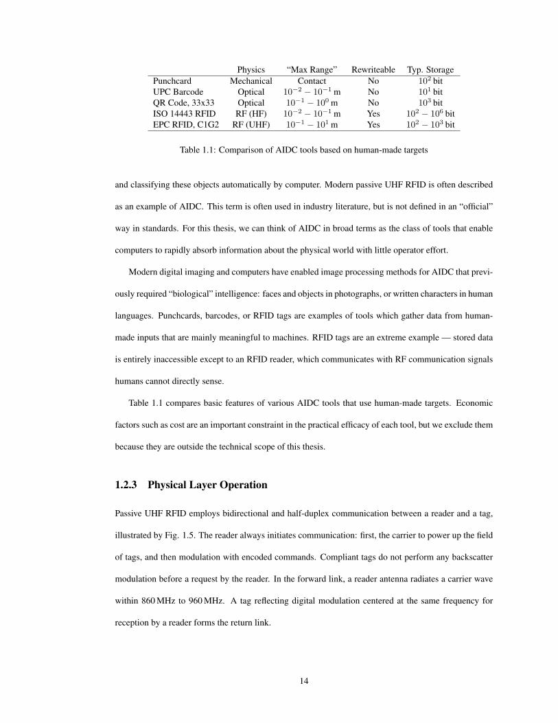
Physics “Max Range” Rewriteable Typ. Storage
Punchcard Mechanical Contact No 102 bit
UPC Barcode Optical 10−2 − 10−1 m No 101 bit
QR Code, 33x33 Optical 10−1 − 100 m No 103 bit
ISO 14443 RFID RF (HF) 10−2 − 10−1 m Yes 102 − 106 bit
EPC RFID, C1G2 RF (UHF) 10−1 − 101 m Yes 102 − 103 bit
Table 1.1: Comparison of AIDC tools based on human-made targets
and classifying these objects automatically by computer. Modern passive UHF RFID is often described
as an example of AIDC. This term is often used in industry literature, but is not defined in an “official”
way in standards. For this thesis, we can think of AIDC in broad terms as the class of tools that enable
computers to rapidly absorb information about the physical world with little operator effort.
Modern digital imaging and computers have enabled image processing methods for AIDC that previ-
ously required “biological” intelligence: faces and objects in photographs, or written characters in human
languages. Punchcards, barcodes, or RFID tags are examples of tools which gather data from human-
made inputs that are mainly meaningful to machines. RFID tags are an extreme example — stored data
is entirely inaccessible except to an RFID reader, which communicates with RF communication signals
humans cannot directly sense.
Table 1.1 compares basic features of various AIDC tools that use human-made targets. Economic
factors such as cost are an important constraint in the practical efficacy of each tool, but we exclude them
because they are outside the technical scope of this thesis.
1.2.3 Physical Layer Operation
Passive UHF RFID employs bidirectional and half-duplex communication between a reader and a tag,
illustrated by Fig. 1.5. The reader always initiates communication: first, the carrier to power up the field
of tags, and then modulation with encoded commands. Compliant tags do not perform any backscatter
modulation before a request by the reader. In the forward link, a reader antenna radiates a carrier wave
within 860 MHz to 960 MHz. A tag reflecting digital modulation centered at the same frequency for
reception by a reader forms the return link.
14

Figure 1.5: The two links of half-duplex ISO 18000-6C RFID communication, shown for the monostatic
(shared transmit and receive antenna) case. In the forward link (a), a reader sends a modulated request
to a tag, which rectifies the incident wave to power its circuitry. In the return link (b), the tag reflects a
modulated reply to the reader.
15

tx data
3 dB0o
3 dB90o
Irx data
3 dB
Q Simple reader RF frontend Tag RF frontend
tx data
Vdc+
Vdc-
rx data
Dickson chargepump
Figure 1.6: Examples of simple RF frontends for readers and tags. Forward link modulation is based
on ASK, requiring only power envelope detection in the tag. Return link modulation is generated by
shorting the tag antenna load to reflect back to the reader, which detects the backscatter with an IQ
demodulator.
RF Hardware
Block diagrams of simple but functional RF frontends of passive UHF RFID hardware are shown in
Fig. 1.6. Readers usually transmit between about 20 dBm to 30 dBm (peak) into an antenna with about
4 dBi to 8 dBi of gain. The lower bound of these numbers affects the desired read range and antenna
beam width, and the upper end is determined by national regulations. In the United States and Europe,
the product of these (sum of dB quantities) is limited to 35 dB to 36 dB, and available power into the
reader antenna is limited to about 30 dBm. Modern passive UHF RFID tag chips need to absorb around
-15 dBm to turn on. The transducer loss between a fixed reader’s coaxial RF output and a tag chip is
therefore limited to about 45 dB at 30 dBm transmit power or 35 dB loss at 20 dBm transmit power. This
is discussed more in Chapter 3.
After a brief power-up period, the reader modulates the carrier with data according to RFID protocols
at 40 kbps to 160 kbps. Modulation from the reader is usually amplitude-shift keying (ASK) or phase-
reversal ASK (ASK with 180 phase shift between binary symbols). At a fixed data rate, phase-reversing
amplitude-shift keying (PR-ASK) uses less bandwidth at a given data rate than the ASK. Standards
also permit single-sideband ASK, but this is rare in practice because it requires a more expensive IQ
modulator in the reader transmitter.
16

The tag rectifies some of the RF power that is available from its antennas to supply power. Rectifi-
cation is generally realized with a simple and compact but inefficient Dickson charge pump [25]. Since
there is no battery on the tag, the tag turns off soon after the reader carrier is turned off (assuming no
other source of strong radiation), unlike the more complicated but more capable sensor platforms with
batteries and power management (as proposed in, e.g., [26]). The ASK-based modulation from the reader
varies the transmit power and thus the power available for harvesting by the tag; the tag therefore needs
some shunted power supply capacitance to sustain power for up to about 10 µs during modulation.
The tag reflects power to the reader by shorting the shunted field-effect transistor (FET) at the antenna
terminals with the “tx data” signal. Switching between the short and the power harvesting state enables
data rates between 40 kbps and 640 kbps. Chapter 2 will demonstrate that this realizes the mixing as
illustrated by Fig. 1.2. Shorting the antenna to create this modulation also shorts the charge pump and
therefore the tag power supply. The buffer capacitor at the DC output sustains tag power here just as in
the forward link.
The LO in both links comes exclusively from inside the reader, which must set the carrier frequency
within the limitations of appropriate national RF emissions regulations. In the United States, a reader
carrier frequency must be at at one of 50 channels spread evenly between 902.75 MHz and 927.25 MHz,
switching (“hopping”) to each one and dwelling no more than 400 ms. In most of Europe, readers may
only transmit full power in one of 10 channels between 865.6 MHz and 867.6 MHz, and do not have to
hop but must wait for an unused channel before transmission. These are only examples; other areas of
the world have still different rules. Readers sold commercially are often able to operate in only one of
these regions. In contrast, passive tags are designed for matching and backscattering across the entire
860 MHz to 960 MHz band and are therefore usable internationally.
A challenge that was mitigated in some second-generation RFID reader products was desensitization
caused by a strong received carrier. Since the carrier does not convey data, it is not useful for commu-
nication. Unfortunately, some carrier leaks from the transmitter into the receiver, primarily because of
imperfect antenna matching and circulator isolation in monostatic systems or by antenna-to-antenna cou-
pling in bistatic systems. The result is that the leaked power may reasonably be over 60 dB stronger than
17

received modulation, so a low-noise amplifier (LNA) saturates and fails to amplify transponder signals.
The receiver desensitizing signal is known in the literature as simply the carrier, leakage, or the leaking
carrier.
The approach taken to solve this problem in long-range RFID readers is an adaptive feed-forward
cancellation, illustrated by Fig. 1.7a. Papers that propose these systems refer to them equivalently as a
leakage canceller [27, 28], isolator [29, 30], or carrier suppression system [31]. The ability to suppress
this carrier is characterized by its tx-rx isolation (in decibels) [27, 30, 32], which may be the absolute
system isolation (transmitter carrier power divided by receiver carrier power) or as relative improvement
realized by the isolator. The author built a prototype in 2007 during early work on detection, pictured
mounted next to bistatic antennas in Fig. 1.7b, which increased isolation by 60 dB.
Data Protocol and Capabilities
Signaling from the reader in the forward link controls the signal rate and timing of both the forward and
return links, and transmits commands to the field of tags. There are only a few simple commands:
(1) “Singulation:” an inventory of all or some of the tags that respond to the reader.
(2) “Read:” retrieving data from memory on one tag.
(3) “Write:” storing data into nonvolatile tag memory of one tag.
A reader usually performs singulation before a read or write command or any change of carrier frequency
to identify the tags that are available for reading or writing. For inventory purposes, singulation is the
most common command and by far the slowest.
Typical tags have a 96 bit identification number. At the maximum 640 kbps data rate, we can imagine
“ideal communication” (nonstop communication from one tag at a time with no symbols wasted on the
protocol) could singulate tags faster than 6000 per second. In practice, well-optimized singulation with
passive UHF RFID protocols are limited to a few hundred tags per second, and only in communication
with a large number of tags.
18

Ant 1
Ant 2
Detector
Vmag
Vph
Interrogation
ControlSystem
+
C
(a)
(b)
Figure 1.7: General architecture adaptive isolator (a) and a realized prototype constructed by the author
in (b). A computer operates the variable attenuation and phase shift over GPIB with a DC power supply,
adjusting with a steepest descent algorithm until the leaked carrier signal is minimized. The substrate is
a 30 cm × 30 cm square.
19

The reason for the inefficiency is that tags do not generally “know” when to answer to avoid collisions
(simultaneous responses), and a reader does not generally “know” which tags will respond. The solution
to this in passive UHF RFID standards is known as “slotted aloha.” Work since 2004 has investigated the
performance of slotted aloha with additive white gaussian noise (AWGN) [33], multipath fading [34],
and active interference [35]. Other authors have suggested more efficient alternative algorithms with
Markov process modeling [36] or CDMA [37], but so far standards have not adopted these approaches.
1.2.4 Standards
A significant motivation behind this work was to support standards development to promote robust, re-
liable, and interoperable communication in U.S. federal government RFID deployments. Most of this
effort is focused on test methods, which are less complete than the standards that define the communica-
tion protocol and standards.
Communication Protocol
Standards-compliant readers incorporate anticollision, the part of the protocol that enables the reader to
select one tag out of many to respond at a time.
Test Standards
Results from tests that comply with existing standards have the advantage of implicitly conveying mea-
surement details, giving a sense of the accuracy of the measurements and how they might help predict
behavior in realistic use. If the standards give methods that achieve low measurement uncertainty, careful
testing between different labs can validate conclusions by repeating the same tests in their own facili-
ties. At present, test methods in existing standards are continuing to improve, but do not yet detail test
methods necessary for complete device characterization.
Performance test standard ISO/IEC 18046-3 [38] outlines a general test for the threshold field strength
necessary to activate a tag, but offers no specific approach for determining field strength. Tag scattering,
which is becoming a more significant system range constraint as tags improve [39] and especially when
20

interference is present [40], is addressed only in protocol conformance test standards.
The 2006 version of standard ISO 18047-6 [41] prescribes a tag backscattering conformance test
characterized as the difference between the radar cross section values between the tag’s two load mod-
ulation states. The test method calibrates measurements of tag backscattering against the change in
received power caused by adding a thin rod to the test environment. Adding and removing the entire thin
rod calibration standard introduces systemic error by modulating the structural-mode scattering from
the rod, which interacts with multipath in the test environment differently [39] from a tag’s antenna-
mode [42][43] scattering. The use of such an electrically small calibration target requires faith in the
accuracy of the analysis used to compute its radar cross-section (RCS), which makes the measurement
result untraceable to fundamental physical standards of any national metrology laboratory. These errors
may make measurement results challenging to repeat between different testbeds, and as a result some
parties may choose not to undertake the expense of running the tests. This approach can introduce sig-
nificant systemic error by neglecting phase, though many existing papers have discussed how phase can
be included, e.g., [42][43][44].
The 2011 version of the ISO 18047-6 conformance test standard computes “Delta RCS” for a device-
under-test by inserting measurements of range and antenna gain parameters into the radar equation,
incorporating measured phase. The uncertainty of results from this approach has been estimated at
approximately 2 dB in a paper that used a similar approach [45]. With spectrum analyzer backscatter
measurements, however, drift and automatic realignments corrupt the relative accuracy of measurements
of tags taken at different times.
While calibration errors may not introduce problems in comparing tag performance, they will intro-
duce errors in measurements of the absolute signal levels in and out of a reader. To avoid this problem,
at the sacrifice of the generality offered by a “black box” tag characterization, results in this thesis are
from measurements of available power transmitted into and received from the test antennas. Transmitted
power is measured with a directional coupler and power sensor, and backscattered power is measured
with the calibration introduced in [46].
21

1.3 Microwave and Communication Parameter Definitions
1.3.1 Real-valued, Analytic, and Time-Domain Voltages
The veritable cornucopia of available communication test instruments takes advantage of a wide variety
of signal representations. Oscilloscopes show real-valued time domain voltage, spectrum analyzers show
the power spectrum in the frequency domain, and signal analyzers give baseband signals as complex
voltages in the time or frequency domains, as eye diagrams, or as constellations.
A very general tool that helps move between these is Gabor’s complex analytic signal [47]. In partic-
ular, given a general excitation that includes but is not limited to a sinusoidal carrier, the analytic signal
be expressed as a product of “instantaneous frequency” and the complex baseband vector.
Consider a real-valued receiver voltage, v(t). The corresponding complex analytic signal (also
known as complex envelope) is:
V(t) = v(t) + jH [v(t)], (1.1)
where the imaginary part is the Hilbert transformation of v(t),
H [v(t)] = p.v.
∫ +∞
−∞
v(t− τ)
πτdτ. (1.2)
The p.v. denotes Cauchy principal value integration. The inverse transformation from the analytic signal
back to the real-valued signal is v(t) = Re(V(t)).
The Hilbert transform defined here is not well-defined or analytically solvable for all classes of
continuous signals v(t). For narrowband digital signals, however, the transform has some simple key
properties:
(1) Linearity: For signals v1(t) and v2(t) and real constants k1 and k2,
H [k1v1(t) + k2v2(t)] = k1H [v1(t)] + k2H [v2(t)]. (1.3)
The transformation from v(t) to V(t) is therefore also linear.
(2) Sinusoidal transform pair [48][p. 18]:
H [cos(2πft+ φ)] = sin(2πft+ φ), (1.4)
22

for frequency and phase f and φ.
(3) Bedrosian’s product theorem [49, 50]: For two signals v1(t) and v2(t), if v1(t) has no spectral
energy above some frequency f , and v2(t) has no energy below f , then
H [v1(t)v2(t)] = v1(t)H [v2(t)]. (1.5)
This represents is behavior of an ideal lossless and mixing process.
Combining each identity with the definition of the analytic signal makes it possible to decompose
the communication signals into modulation and carrier components. In narrowband communication that
uses a sinusoidal signal as a carrier (like UHF RFID), the complex signal is related to the complex-valued
root mean square (RMS) baseband signal, V (t), as
V(t) =√2V (t)e2πfct. (1.6)
The exponential term is the sinusoidal case of the instantaneous frequency [51]. Other instantaneous
frequency signals are also valid if their spectral power is exclusively at higher frequencies than V (t) [49]
(though certain other cases are valid as well [50]). In the RF mixing process, the instantaneous frequency
represents the LO, the baseband represents the IF, and the analytic signal represents the RF (upconverted
baseband) signal in the communication mixing process.
1.3.2 Fourier Transform
This thesis follows the Fourier transform defined as
F [v](f) =
∫ +∞
−∞
v(t)e−j2πftdt. (1.7)
This is the definition followed by instrument manufacturers in terms of unitary frequency rather than
radial frequency [52–54], avoiding some normalizing factors. The corresponding inverse transform is
v(t) =
∫ +∞
−∞
F [v](f)ej2πftdf. (1.8)
23

This is related to the positive half-space of the transformed analytic signal as [48, p. 9]:
F [v](f) =
12F [V(t)](f), f > 0
F [V(t)](0), f = 0
12F [V(t)](−f) f < 0.
(1.9)
Spectrum analyzers often show power spectral density (PSD) defined only in the positive half-space
of the frequency domain. This includes power from negative frequency components “folded” onto the
positive half space. The PSD of a signal absorbed into a load with impedance Z, with units of power per
frequency, is
PSD[v(t)](f) = 2|F [v(t)](f)|2
Re(Z)
=|F [V (t)](f − fc)|2
Re(Z).
(1.10)
This is the “ideal” continuous PSD, with the factor of 2 discrepancy arising from the RMS definition of
the complex baseband signal V (t). The actual PSD trace displayed on an instrument will be altered by
discritization, compression, uneven frequency response, spurious harmonics, impedance mismatch, and
windowing. It is defined for f ≥ 0 and normalized to the real part of the instrument port impedance,
Re(Z).
1.3.3 Pseudowave Scattering Parameters
Network analysis in this thesis primarily employs “pseudowave” S-parameters. These parameters are
considered in great detail in [55]. They describe steady-state behavior of waves traveling between mi-
crowave networks relative to some reference impedance, Z0. They are equivalent to “traveling-wave”
S-parameters [56] only in transmission lines with characteristic impedance equal to Z0. Dependence on
frequency in this thesis is implicit, and not shown for power or network parameters.
Each Z0 will be assumed real and identical at all ports for this work, to simplify expressions of power.
The incident and scattered pseudowaves at port m are
am = e−jφ0Vm + ImZ0
2√Z0
(incident wave), (1.11)
24

and
bm = e−jφ0Vm − ImZ0
2√Z0
(scattered wave). (1.12)
Vm and Im are time-harmonic voltage and current phasors with defined with RMS magnitudes. These
are waves at the single radial frequency ω = 2πf . The normalization to 2√Z0 allows unit am or bm
to correspond with unit power as |am|2 and |bm|2. The phase rotation φ0 shared by a and b denotes
normalization to an arbitrary zero phase reference.
In these terms, each pseudowave scattering parameter between two ports n and m is
Smn =ambn
. (1.13)
The Smn elements of an M ×N -port network form an M ×N matrix [S].
When all ports are terminated in Z0, Smn are related to incident and scattered power by
Scattered power to Z0 load, port m
Incident power from a Z0 source, port n= |Smn|2 (1.14)
The convention in this text is to refer to reflection coefficients of loaded [S] as ρ with subscripts, and
transmission coefficients of loaded [S] as τ with subscripts. In this case, each port’s load needs to be
specified except m (and n for τ ), which are still referenced to Z0.
The relationship between ρ and a port input impedance, Z, is
ρ =Z − Z0
Z + Z0(1.15)
(with all other ports are terminated in Z0). The ρ looking into port m of a multiport network is the same
as a scattering matrix element Smm only if all ports are terminated in impedance Z0. Detailed analysis
for finding loaded Z and ρ are given in many network theory texts like [56].
1.3.4 Power Wave Parameters
An alternative to pseudowave scattering parameters are power waves [57]. These are compared exten-
sively in [55]. They are popular in RFID literature, and in use by some nonlinear circuit simulation
software like AWR Microwave Office. In some cases they are ambiguously referred to as “reflection
25

coefficients” or “transmission coefficients,” which may cause confusion with pseudowave reflection co-
efficients.
In this network parameter system, each port m is terminated by a physical load, Zm, not the arbitrary
reference Z0. Incident and scattered pseudowaves at port m are [57]
am = e−jφ0Vm + ImZm
2√
ReZm
(incident wave), (1.16)
and
bm = e−jφ0Vm − ImZ∗
m
2√
ReZm
(scattered wave). (1.17)
Like all other phasors in this thesis, Vm and Im have RMS magnitudes. An M × N power scattering
matrix [S] and each element Smn (composed of am or bn) are defined much like [S].
These parameters describe interaction between a network and its load, unlike pseudowaves, which
characterize the network when loaded with some Z0 that can be chosen arbitrarily. The power wave
reflection coefficient Smm is related to available reflected power from port m terminated in Z by
Reflected power absorbed by generator
Available incident power= |Smm|2 =
∣
∣
∣
∣
am
bm
∣
∣
∣
∣
2
=
∣
∣
∣
∣
Z − Z∗m
Z + Zm
∣
∣
∣
∣
2
. (1.18)
The result is a compact representation of reflected and transmitted power in simple one-ports. Power
delivered into port m is
Power delivered to port m
Available incident power= 1− |Smm|2. (1.19)
The compactness of power absorption expressions with power waves belies underlying complexity
in their use. Changing any Zm at a non-isolated port of [S] causes the power normalization of each
am and bm to change as well. The wave parameters in (1.16) and (1.17) depend on both Zm and Z∗m;
this means that a graphical representation needs an extra dimension to represent ∠Zm, in addition to the
two on a Smith chart. There is no “3D Smith chart” of this type in broad use [58] (the extra dimension
in [59] is to support |ρ| > 1). There are also no instruments that directly measure power waves, so
they have to be computed indirectly from pseudowave measurements with a network analyzer. This
complicates measurement uncertainty estimation, which is understood and expressed primarily in terms
of pseudowaves [60, 61].
26

These challenges are surmountable and for some uses may be outweighed by the convenience of
equations (1.18) and (1.19). In this work, we mainly use power waves to convey conceptual problems
compactly, but also give expressions in terms of more measurable pseudowaves. This lets us leverage
mature test engineering and metrology and use well-trodden S-parameter network analysis.
1.3.5 Time-Harmonic Linear Power Absorption and Mismatch
The subject of power normalization with respect to voltages and currents can become thorny and gen-
erally unpleasant when waves are involved. Other authors already discuss this in great detail (see for
example [62, pp. 77-79]). Combining too many normalization conventions could complicate notation
and distract from the main ideas of this thesis. Some effort is made here, therefore, to define signal
quantities clearly, so physical meaning is clear, and theory and simulation and measurement results can
all be compared directly.
This thesis defines voltages solely at the interface between networks, as illustrated in the phasor
domain Fig. 1.8(a,b), never as Thevenin equivalent circuits like Fig. 1.8(c). These circuits are truly
equivalent only in the sense that they excite in the same voltages and currents as in the actual source.
They are nonphysical, however, in the sense that an RF generator is never actually realized as a zero-
impedance voltage source in series with a lossy resistor. Their impedances behave as a voltage divider,
reducing the voltage V presented across ZL compared to the Thevenin voltage, according to Fig. 1.8(c).
Voltage and current phasors and baseband signals are defined as RMS to match the convention of
instrument manufacturers — this is a metrology-focused thesis, after all. This has the side-effect of
simplifying normalizing constants: power delivered into ZL is simply
Power delivered into Z = Re(VrmsI∗rms) =
|Vrms|2Re Z
. (1.20)
The relationship between this “available power,” the power available to a Z0 load (by pseudowaves
with magnitudes |b| or |a|), and the power actually delivered into a load depends on the generator and
load impedances. Assume that our generator and load of Fig. 1.8 have reflection coefficients ρG and ρL.
The power wave reflection coefficient between this feed and generator is ρ.
27
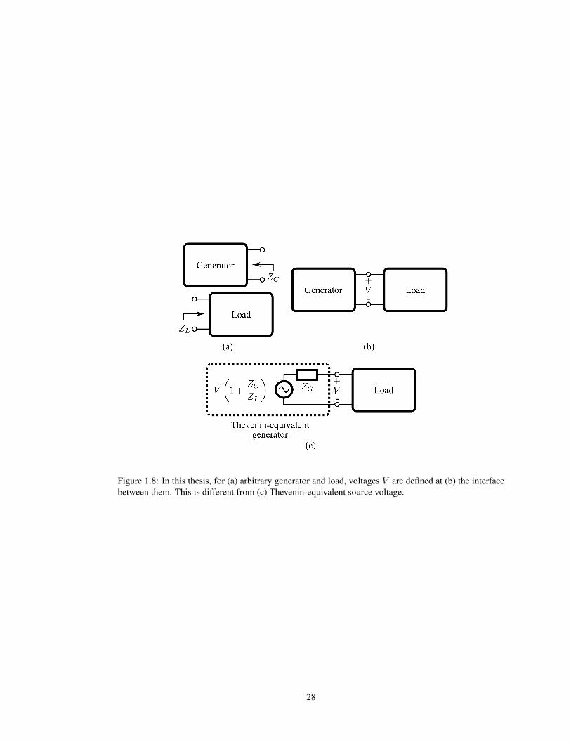
Figure 1.8: In this thesis, for (a) arbitrary generator and load, voltages V are defined at (b) the interface
between them. This is different from (c) Thevenin-equivalent source voltage.
28

The “conjugate match efficiency” is defined as [56]:
Power delivered into ZL
Power delivered if ZL = Z∗G
=(1− |ρL|2)(1− |ρG|2)
|1− ρLρG|2,=
4Re(ZL)Re(ZG)
|ZL + ZG|2= 1− |ρ|2. (1.21)
This is between 0 (no power delivered) and 1 (the conjugate match case).
The “Z0 match efficiency” is:
Power delivered into ZL
Power delivered if ZL = Z0==
1− |ρL|2|1− ρLρG|2
. (1.22)
Despite the name, this can be larger than 1 when |1− ρLρG| < 1.
This lets us define when we might be able to assume the source and receiver transfer all available
power. A tight definition of “well-matched” for this thesis is 20 dB of return loss at both the receiver
and where it is connected; this corresponds to match efficiency greater than 96%, or less than 0.2 dB of
mismatch loss. This is in many cases reasonable.
The convention in this work is that variables labeled P with subscripts mean “available power to a
conjugate-matched load.” The sole exceptions are PL and Pbs, power delivered into the tag chip and
backscattered power delivered into the reader receiver.
1.4 Measurement Uncertainty
Measurement uncertainty is the quantitative complement of measurement accuracy. It is qualitatively
equivalent to say a measurement has “small uncertainty” as to say it is “very accurate.” Unlike accuracy,
however, there is a more defined (though not rigorous) quantitative practice underpinning the calcula-
tion and expression of measurement uncertainty. This section offers a brief overview of the concept of
uncertainty as a basis for its use in the remainder of the thesis.
The practice of estimating and expressing measurement uncertainty is described for international
purposes by the Bureau International des Poids et Mesures (BIPM) guide on uncertainty of measurement
(“GUM”) [63], and within National Institute of Standards and Technology (NIST) (where much of the
work for this thesis was performed) by Technical Note 1297 [64]. Uncertainty statements performed
in this thesis are computed and expressed according to the processes described in these documents as
carefully as possible.
29

We expect that there is in general more than one kind of error contributing to the total uncertainty
of a physical measurement. Each source of error could be systematic (deterministic and predictable),
or random (non-deterministic or stochastic). A systematic error that can be identified and modeled can
often be removed analytically from the measurement result. If the measurement involves independent
samples of a zero-mean random error, averaging can mitigate its effect on measurement uncertainty.
Repeatability (or precision) is the complement of these random components of uncertainty: the extent to
which a measurement gives the same result when repeated many times.
Classifying a source of error as systematic or random depends in part on whether it is measured as
part of the experiment. In microwave network measurements, for example, mismatch can alter the power
absorbed by a power sensor. If the circuit is invariant with time, the mismatch effects might characterized
with a network analyzer to be de-embedded from the final measurement result, removing it as a source of
error. On the other hand, if the network is a pair of antennas in an anechoic chamber, multiple reflections
between the antennas change as a function of the distance between them; sweeping antenna position thus
results in hard-to-predict error in measured power that can be assumed random.
Consider a measurement result represented by a random variable Y . The measurement process is
modeled by some function f(X1, X2, ..., Xn), which ideally incorporates all n different sources of vari-
ability or error. Each source of error has a standard deviation which we call the standard uncertainty
ui = u(xi). If these errors are uncorrelated, the combined uncertainty of the measurement result y,
uc(y), is computed as
uc(y) =
√
√
√
√
n∑
i=1
(
δf
δxiu(xi)
)2
. (1.23)
This is the law of propagation of uncertainty simplified for uncorrelated Xi. Each sum term is the
sensitivity of the of xi and the variance of Xi.
Approaches to estimating each u(xi) are classified into two types. Statistical approaches are known
as “type A;” these are based more on analysis of the data than on physical models for the error terms.
This could be as simple as measuring the standard deviation of a data series. “Type B” estimates of
u(xi) come from an assumed probability distribution for Xi. Type B is often very practical in microwave
measurement: the thermal noise of a voltage signal is accurately described by the normal distribution,
30

mismatch error is accurately described by the U-shape distribution [65][66], and digitized rounding error
is uniformly distributed. Thus, estimates of uncertainty in this work are generally “type B.” Uncertainty
estimation is so rough in part, however, because types “A” and “B” are both accepted approaches but
may give different u(xi).
Despite the firm-sounding name, the “law” of propagation of uncertainty is a first-order Taylor series
approximation that is only accurate if either:
(1) the errors Xi with the largest u(xi) are normally distributed; or,
(2) there are a large number of Xi with similar u(xi),
by the central limit theorem. When one of these conditions is assumed valid for a meaningful uc(y),
Y can be assumed distributed normally. In this case, uc(y) is the standard deviation of Y , so we have
only 68% confidence that the measurement is within ±uc(y) of the “correct” value. Scaling uc(y) by a
coverage factor k > 1 gives the expanded uncertainty of our measurement, U :
U = kuc(y), (U ≥ 0). (1.24)
The value k = 2 is a common implicit choice in microwave measurements, corresponding to about 95%
confidence that the “true” value of the measurement y lies in interval [y − U, y + U ], if combined error
is normally distributed. Some older papers use k = 3 that suggests 99.7% confidence that y lies in the
same interval (at the expense of larger reported U ). This thesis uses k = 2.
Microwave measurements are often given as ratioed unitless quantities on a logarithmic scale as
decibels. The relative expanded uncertainty is simply
Ur =U
|y| , (1.25)
depending on the same coverage factor as U . When k = 2, Ur describes the probability that y of an ideal
measurement of y normalized to the actual measurement of y is
∣
∣
∣
∣
y − U
y
∣
∣
∣
∣
<
∣
∣
∣
∣
Ideal y
y
∣
∣
∣
∣
<
∣
∣
∣
∣
y + U
y
∣
∣
∣
∣
(1.26)
or
|1− Ur| <∣
∣
∣
∣
Ideal y
y
∣
∣
∣
∣
< |1 + Ur| . (1.27)
31

with about 95% confidence. When y is a power quantity, we can also convert to decibels,
10 log10 |1− Ur| < 10 log10 |Ideal y| − 10 log10 |y| < 10 log10 |1 + Ur| . (1.28)
For small errors, these bounds can be expressed as
−UdB < |Ideal y| (dB) − |y| (dB) < +UdB (approximate). (1.29)
When Ur < 0.25 (UdB < 1 dB), this approximation is valid and UdB ≈ 4Ur to within 0.03 dB. The
magnitude of measurement errors in this work is often small, so uncertainty estimates for measurements
in dB are computed according to (1.29). On the order of Ur > .2, the absolute value of the two bounds
are no longer approximately equal, and the supplied approximation for UdB increases in error.
As a final note on uncertainty, a side-effect of the large numbers of assumptions in uncertainty es-
timation is that U is a subjective result. An estimate combined with large n is likely to need so many
assumptions that they are difficult to list. The practice used in this document is to assume the largest
(worst) reasonable value for each u(xi) to give conservative uc(y) and thus U .
1.5 Thesis Scope and Structure
The theoretical focus in this work is communication with binary-modulated passive backscattering transpon-
ders. This class of devices currently includes RFID, but in the near future the cost benefits to passive
backscatter may see its use in other common applications like wireless sensing.
Practical application of the theory is to passive RFID tags with fixed readers following EPC Global
Class 1 Generation 2 or ISO 18000-6C standards (which are considered identical, and synonymous with
“passive UHF RFID” for the purposes of this thesis). This class of system is of interest for the following
reasons:
• Most commercial RFID systems operating in the far field follow these standards.
• Many readers and tags from different vendors are marketed as compliant with these standards. This
creates uncertainty about interoperability and performance when readers and tags from different
vendors must be used together, which may benefit from improved test practices.
32

• Fixed readers operate unsupervised during normal use, so there is no human operator to work
around reliability problems. More extensive tests and modeling are therefore necessary to ensure
robust operation, but there is little relevant literature on this subject.
• A key feature of fixed readers is long range. At long range, backscattered tag response power is
weak, which can strain link range and reliability. This imposes fundamental limitations on these
communications that have not studied in detail.
• A fixed reader is usually more costly than a mobile reader. Improved understanding of the limita-
tions of these fixed-reader systems may therefore have the greatest influence on end-user costs and
benefits, compared to systems that use mobile readers.
Within this type of system, the goal is to predict backscatter signal levels into a reader. When the
noise level inside the receiver is fixed, this corresponds to predicting signal-to-noise ratio (SNR) (in low-
interference environments) or signal-to-interference ratio (SIR) (in higher-interference environments)
relative to the tag backscatter. These data, in turn, predict reliability of tag communication and detection
rate when interference is weak. This work approaches this problem with microwave network theory, to
maximize the generality of the solution with arbitrary network blocks representing environmental loss
effects.
The contributions of the remaining chapters toward these goals are organized as follows:
Chapter 2 discusses the most basic link parameter of backscatter modulation, signal power. It is
not explicitly derived in terms of measurable signals by standards or other technical technical literature.
This chapter investigates advantages and disadvantages to defining the modulation power as “classic”
digital ASK or BPSK modulation schemes, and how they can be separated from the large leaked carrier.
Passive UHF RFID encoding makes BPSK independent of the carrier, which simplifies spectral analysis
and ensures that energy is conserved at all reference points for any passive tag modulation loads.
Chapter 3 presents models and characterizations of passive backscatter link power. High-level anal-
ysis of the benefits and risks in the use of RFID requires an understanding of what is possible within the
bounds of physics, standards, and emission regulations. Fundamental power parameters and relation-
ships defined in Chapter 2 enable informed discussion of device characterization and system behavior in
33

free space, and recent movement toward more general analysis based on network theory. This chapter
formulates an alternative, more compact tag backscattering characterization than radar cross-section that
applies in passive systems. With this metric, system designers can find a deterministic minimum bound
to backscatter received from any passive tag under realistic fading conditions with a trivial computation.
Chapter 4 defines test methods for measuring backscatter power with calibration circuits. The devices
and test methods generate reference signals suitable for transceiver or transponder performance tests. For
transponders, approaches are investigated both 1) through fixed-loss coaxial networks and 2) over-the-air
through antennas. For reader testing, a coaxial calibration device reflects adjustable modulation power
into monostatic reader ports. The testbed is overspecified to result in lower uncertainty than required for
realistic commercial device tests in order to rigorously validate the model.
Chapter 5 discusses use of the power measurements in testing transponder backscatter performance.
This chapter compares the accuracy of radar cross section and backscatter figure of merit measurements,
and propagation to estimates of received backscatter power. The received power estimate is always at
least slightly greater than the uncertainty of the tag backscatter metric used to estimate it. Uncertainties
for radar cross section measurements contribute negligibly to uncertainties in received power, as long as
multipath is weak. In contrast, uncertainty of a minimum backscatter power bound estimate is the same
as figure of merit measurement uncertainty. Thus, estimates of minimum backscatter power from the
figure of merit are always more accurate than estimates of backscattered power from σ∆.
Chapter 6 gives techniques for reliable system design based on the device tests. With validated
theory and measurement ability, we can now analyze system behavior of off-the-shelf commercial readers
and tags. Use of the minimum backscattered tag power bound predicted in Chapter 3, coupled with
information about the sensitivity and interference rejection of the reader, allows system designers to
determine whether channel diversity schemes are necessary. Calibrated measurements of 20 different
commercial tags suggest long-term trends of increasing communication range but lower inventory rate
between fixed readers and passive tags. Finally, the application to RFID culminates with a system design
approach for ensuring reliable backscatter communication.
Chapter 7 concludes the thesis with a brief summary, directions for future work, and extolls the
34

author’s peer-reviewed publications.
Finally, Appendix I provides a table of link variables as a reference for the preceding chapters.
35

Chapter 2
Backscattered Receiver Signals and
Power
Professor Benson: “Young fellow, you and the
others have to see and hear before you can know. I
have one advantage over all of you: calculus!”
“Il Pianeta degli Uomini Spenti” (1961)
Communication by backscatter is less broadly understood in the technical community than by pow-
ered transmission. This no surprise, since its use is rare. A side effect, however, is that basic signal and
power definitions remain vague and undefined in standards, so there is no widely-accepted guidance or
reference on the meaning of common parameters.
In backscatter literature, for example, the terms ASK and BPSK are typically implicitly assumed to
refer to a digital signal constellation made of the two power wave states that realize load modulation
[67, 68]. Current RFID standards [1, 2] explicitly allow tags to respond with either ASK or BPSK but
define neither. The modulation signal received by a interrogator can also be defined many different
ways which have not been discussed explicitly in the literature. Prior art has assumed at least three
different normalizations without justification. The result is that Green and Nikitin [69, 70] compute
“backscattered power” as twice that of Skali (and derived standards) [41, 44], which itself gives twice
36

the result of Karthaus and the author of this thesis [68, 71]. Without guidance from a standard blessing
one of these, the same quantity could conceivably differ by a factor of up to 4 (6 dB) among different
sources.
This chapter investigates the validity and spectral properties of various definitions of power given the
requirement of power conservation at network interfaces. The basis is a model of backscatter modulation
through microwave networks built with basic signal and network theory. The resulting contribution of
this chapter is an explicit and carefully justified definition for modulation power in terms of receiver
baseband signals. This definition then becomes the basis for discussion of backscattered power in later
chapters. This type of analysis is necessary in the broader technical community to inform any future
official decision about defining signal parameters.
2.1 Binary Load-Modulation States through Microwave Networks
A network model of a switched impedance loading a microwave network is illustrated in Fig. 2.1,
following the topologies of [43] and [46]. This could be viewed as a complete passive RFID system
model without loading by the interrogator (or with a Z0-matched interrogator). The network parameters
(besides impedances ZL) are pseudowave S-parameters as defined in Section 1.3.3.
The three-port pseudowave network E represents the general case of any transmission effects be-
tween a transceiver and the load modulation. The transceiver could be bistatic by separate transmission
and detection at ports 1 and 2, or monostatic by transmitting and detecting at either port 1 or port 2 and
loading the other with Z0. Port 3 is the interface between the tag’s chip and antenna. The interrogator
transmits into port 1 or 2. The transmission effects in E could include (but are not limited to) wireless
propagation, test circuits, antennas, or transmission lines.
If the two networks are disconnected (Fig. 2.1a), transmission coefficients between the loaded ports
in the reciprocal transmission are E23 = E32 = b3/a2 and E31 = E13 = b′3/a′1 (the notation for
pseudowaves b′ and a′ indicates port 3 of E is not attached to ZL). The reflection coefficients of the
backscattering antenna and the modulator are E33 = b′3/a′3 and ρL = bL/aL, respectively. E and ρL
are measurable by network analyzer if the modulator and transmission networks E can be disconnected
37

Port
2Po
rt 1
Port 3(a) disconnected
Port
2Po
rt 1
Port 3
(b) connected in monostatic operation
Port
2Po
rt 1
Port 3
(c) connected in bistatic operation
Figure 2.1: Reflection and transmission coefficients presented to a Z0-matched interrogator (a) dis-
connected from and (b,c) loading the 3-port pseudowave network [E] in monostatic and bistatic. The
modulator switches between ρL → ρL1, ρL2 (impedances ZL → ZL1, ZL2).
38

into well-defined networks.
If the two networks are connected (Fig. 2.1b), ports 1 and 2 of E present loaded reflection coefficients
ρ1 and ρ2 for monostatic detection. Bistatic detection into a Z0-matched transceiver is characterized
loaded transmission coefficients τ21 (excited at port 1) or τ12 (excited at port 2).
2.1.1 Bistatic Operation
Consider bistatic operation excited at port 1 of E as in Fig. 2.1c and detected at port 2. The transmission
coefficient representing this process depends on the modulator load, τ21 → τ21(ρL). An expression for
τ21(ρL) in terms of E, some arbitrary modulation load ρL, and the incident pseudowave is [56, p. 108]:
τ21(ρL) = E21 + E31E23ρL
1− E33ρL, (2.1)
assuming that port 2 is isolated from port 1 or nontransmitting. Equivalently, τ21 can be defined in terms
of transmission at port 2 and reception at port 1 by reversing subscripts 1 and 2.
Consider the two different load states, ρL → ρL1, ρL2. Through dependence on ρL, τ21(ρL) also
takes two states. The change in the transmission coefficient presented between ports 1 and 2 is
∆τ21 = τ21(ρL2)− τ21(ρL1) =E31E23
(1− E33ρL2)(1− E33ρL1)(ρL2 − ρL1). (2.2)
The average between the two states is τ :
τ21 =τ21(ρL2) + τ21(ρL1)
2
= E21 +E31E23
(1− E33ρL2)(1− E33ρL1)(E33ρL2ρL1 +
ρL2 + ρL1
2).
(2.3)
The change and mean of the transmission coefficient are related to τ21(ρL2) and τ21(ρL1) as,
τ21(ρL1) = τ21 +1
2∆τ21
τ21(ρL2) = τ21 −1
2∆τ21.
(2.4)
The two states are thus centered at τ21 on the complex plane and offset by ±∆τ21/2.
2.1.2 Monostatic Operation
The monostatic equivalent of (2.2) at port 1 for the loaded reflection coefficient, ρ1(ρL), is [72]
ρ1(ρL) = E11 + E31E13ρL
1− E33ρL. (2.5)
39

The change in reflection coefficient between these states is
∆ρ1 = ρ1(ρL2)− ρ1(ρL1) =E31E13
(1− E33ρL2)(1− E33ρL1)(ρL2 − ρL1). (2.6)
The change of subscripts and variables from (2.3) gives the average between the states as
ρ1 =ρ1(ρL2) + ρ1(ρL1)
2
= E11 +E31E13
(1− E33ρL2)(1− E33ρL1)(1
2E33ρL2ρL1 +
ρL2 + ρL1
2).
(2.7)
The mean and difference also decompose into ρ1(ρL2) and ρ1(ρL1) like τ21:
ρ1(ρL1) = ρ1 +1
2∆ρ1
ρ1(ρL2) = ρ1 −1
2∆ρ1.
(2.8)
The states are thus centered at ρ1 on the complex plane and offset by ±∆ρ1/2.
Observe that the only difference between this monostatic derivation and the bistatic derivation is that
subscripts that refer to port 2 have been renumbered to 1.
2.2 Backscatter as a Receiver Signal
2.2.1 Signal Anatomy
Consider an ideal and Z0-matched transceiver. We showed in the previous section that the expressions for
ρ1,2 and τ21,12 take the same form and differ only in subscript indexing. If the Z0-matched transceiver
transmits a wave into either port 1 or 2, the corresponding port has a voltage phasor of Vtx/√Z0 by
(1.11) across its terminals. The receiver in the ideal transceiver outputs the complex baseband voltage,
V , related to the scattered pseudowave b/√Z0 exactly by (1.12), at either port 1 or 2. Thus, (2.5) and
(2.1) relates V and Vtx with ρL and E:
V (ρL) = VtxE11 + VtxE31E13
(
ρL1− E33ρL
)
(monostatic)
V (ρL) = VtxE21 + VtxE31E23
(
ρL1− E33ρL
)
(bistatic),
(2.9)
Each discrete ρL state therefore corresponds with a steady-state received voltage phasor, V . Note that
V (ρL) is the steady-state voltage; physical time-varying V (t) include transient effects from the propaga-
40

tion environment, finite switching time in ZL, and frequency-dependent circuit mismatch effects. Like
ρ1,2 and τ21,12, binary states of V can be expressed as a mean and a difference V and ∆V .
The terms VtxE11 and VtxE21 are invariant with ρL, and in our ideal receiver contribute only to V
and not ∆V . In physical circuits, the invariant term is often much larger than the term on the right. This
term therefore usually dominates V .
The more complicated terms on the right of (2.9) determines ∆V , but in general also contributes
to V . The magnitude of the backscattered signal ∆V is proportional to the magnitudes |E31,13| and
|E32,23|. The ∆V has a phase that also depends E and ρL, but that is not important for communication
(more so for tag position estimation [73]).
Thus, we expect that a received signal will change with ρL, but also contain constant independent
components that may be much larger than the component associated with ρL.
2.2.2 Receiver Signals in the Time Domain
Let the load vary with time, ρL → ρL(t), producing time-varying received signal V → V (t). The
time-varying baseband has a modulation component Vbs(t) and interfering constant component Vleak, so
V (t) = Vleak + Vbs(t) (monostatic or bistatic). (2.10)
The analytic signal corresponding to the modulation, Vbs(t), is
Vbs =√2Vbs(t)e
j2πfct, (2.11)
recalling that baseband voltage phasors in this thesis are defined as RMS.
The analytic signal corresponding to the scattered wave into the matched receiver is therefore
V = Vleak(t) + Vbs(t)
=√2ej2πfct(Vleak + Vbs(t)).
(2.12)
The real-valued time domain voltage at the receiver, v(t), is related to the analytic signal as
v(t) = Re(V) =√2 (|Vleak| cos (2πfct+ ∠Vleak) + |Vbs(t)| cos (2πfct+ ∠Vbs(t))) . (2.13)
This is the signal that would appear on an ideal Z0-matched oscilloscope measurement trace.
41

Figure 2.2: Examples of digital modulation constellation diagrams, comparing ideal (a) amplitude-shift
keying and (b) biphase-shift keying against (c) signals received at a interrogator with realistic leaked
components.
2.2.3 Signal Decomposition
A fundamental problem in defining modulation power is separating V into the self-interfering leakage
component, Vleak, and a backscatter modulation component, Vbs(t). Consider first the two basic types
of binary digitally-modulated symbol keying, ASK and BPSK. Their signal constellations [74] are illus-
trated on Fig. 2.2(a,b). The points V1 and V2 represent the two baseband states on the complex plane.
In contrast, a more realistic constellation V for our received backscatter signal illustrated in Fig. 2.2(c).
As illustrated, pure ASK requires V1 = 0 or V2 = 0, and BPSK requires |V1| = |V2|, so V (t) is neither
ASK nor BPSK.
Instead, we can define Vleak so that the remaining signal component is purely ASK or BPSK. This
is illustrated in Fig. 2.3.
The “offset ASK” decomposition is shown in Fig. 2.3(a). Let the “leaked” offset state be defined as
Vleak = V2. This makes the decomposition appear as
Vleak (ASK case) = V2
Vbs states (ASK case) = 0, V1 − V2 = 0,∆V .(2.14)
The V2 and ∆V here characterize the carrier and modulation amplitudes of the V constellation, respec-
tively.
42

Figure 2.3: A digitally modulated baseband backscatter signal can be decomposed into V (t) = Vbs(t) +Vleak as (a) offset ASK or (b) offset PSK.
Next, consider the “offset BPSK” definition as in Fig. 2.3(b).
Vleak (BPSK case) =1
2(V2 + V1) = V
Vbs states (BPSK case) = ±1
2(V2 − V1) = ±1
2∆V.
(2.15)
This is an even-odd decomposition of V . This time, V and ∆V/2 are the carrier and modulation com-
ponent amplitudes.
So far, defining received binary modulation encoding as either ASK or BPSK is legitimate for arbi-
trary ρL1 and ρL2. The choice of definition determines both Vbs(t) and Vleak, so the power contained
in each component depends on this definition of received modulation encoding. Statements of digitally-
modulated backscatter power therefore need either an implicit (for example, by use of standards) or
explicit statement associating the power quantity with one of these definitions.
2.2.4 Frequency-Modulated Encoding in Passive UHF RFID
Defining Vleak and Vbs in terms of baseband modulation states in the time domain is convenient for de-
scribing RFID-specific communication. Currently, standards electronic product code (EPC) class 1 gen-
eration 2 (C1G2) and ISO 18000-6C agree on the same frequency modulation scheme for interrogator-
to-tag communication. The “bi-phase space” symbol encoding defined by these standards is illustrated
in Fig. 2.4.
At the beginning of each new symbol, the signal polarity switches. The maximum signal switching
rate in this scheme is called “link frequency” in standards, and abbreviated here as fm. The symbol
43

rate is fm/M [1], where the signal parameter M is the number of subcarrier cycles per symbol. The
parameter M = 1 corresponds to FM0, though the switching behavior is opposite from Miller encoding:
FM0 switches at the maximum rate for data 1, and Miller switches at the maximum rate for data 0.
Increasing M moves communication sidebands away from the carrier. This reduces co-channel in-
terference, but also the data rate. It is effectively repeating each symbol several times, increasing the
integration time the interrogator receiver can use to improve the SNR and reduce the link error rate.
2.2.5 Passive RFID Backscatter Modulation in the Frequency Domain
Microwave system theory and measurement are most often performed in the frequency domain. In
this work, backscatter spectral characteristics will specifically apply to analysis of mismatch, system
bandwidth requirements, and receiver filter designs. It will also help interpret measurement traces on a
spectrum analyzer.
The ASK Definition
Equation (2.14) defines the ASK component as switching between Vbs(t) = 0,∆V . Standardized
passive UHF tag backscatter spends nearly equal time in each state, so the time-average of Vbs(t) will
be about ∆V/2 for long FM0- or Miller-encoded data streams. The ASK definition of modulation will
therefore contains a carrier component equal to half of the total modulation power.
An instructive signal to examine is an infinite train of FM0 “1” symbols (hexadecimal value FFFFFFFF...)
or Miller “0” (hexadecimal 00000000...). This is a square wave with a Fourier sine series represen-
tation [75, pp. 111-113],
Vbs(t) =∆V
2
+∞∑
n=−∞
cn sin(n2πfmt), (2.16)
with coefficients
cn =
jπn (−1)(|n|−1)/2, (n odd)
0, (n 6= 0 and even)
12 , (n = 0).
(2.17)
Note that the time-averaged component, which corresponds with cn = 0, is not zero.
44

M=4
M=8M=2
0
1
FM0
0
1
0
1
0
1
Time
1/(Link Frequency) 4/(Link Frequency)
2/(Link Frequency) 8/(Link Frequency)
Figure 2.4: RFID tag backscatter digital encoding for FM0 and the various allowed Miller parameters
M = 2, 4, 8 [1].
45

(a)
Strong ASK carriercomponent
(b)
Figure 2.5: Spectral representation of the modulation component for a simplified ASK square pulse train
and backscattered FM0 tag modulation for the arbitrary hexadecimal value DEADBEEF in (a) the time
domain and (b) the frequency domain.
46

Let the integration bounds on our Fourier transform for this infinite pulse train approach T1 → −∞
and T2 → ∞. Applying the transform pair F [sin(f0t)] = −jπ[δ(f − f0)− δ(f + f0)] to each sum term
of (2.16) gives the transformed baseband signal as
F [Vbs(t)](f) =∆V
2
+∞∑
n=−∞
cnδ(f − nfm). (2.18)
Frequency-shifting the baseband to the carrier for the modulated RF signal vbs(t) gives
F [vbs(t)](f) =
+∞∑
n=−∞
cnδ(f − fc − nfm). (2.19)
Like the baseband, the separation between baseband harmonics is determined by the switching rate fm.
Since c0 = ∆V/4, there is a signal at the carrier, even though this is the modulation component. In
the frequency domain, this overlaps with the leaked component, so the two are not spectrally independent.
Adding and subtracting the two will introduce interference depending on their relative phase.
Figure 2.5 compares this spectrum of vbs(t) as a train of FM0 “1” values against a numerical trans-
form of an arbitrary 32-bit value. The switching rate of the modulation is fm = 640 kHz, the maximum
rate permitted by RFID standards. As predicted, the carrier component is about ∆V/4. The “0” symbols
in the arbitrary-valued signal switch at a different rate than “1” symbols give the “slurred” sidebands.
The BPSK Definition
In the BPSK case, Vbs(t) switches between ±∆V/2.
Equal time in each state results in a near-zero DC component of Vbs(t), but with the same sidebands
as ASK. The corresponding Fourier coefficients are therefore
cn =
jπn (−1)(|n|−1)/2, (n odd)
0, (n 6= 0 and even)
0, (n = 0).
(2.20)
With no DC component in Vbs(t), there is therefore no carrier component in vbs(t).
Is this reasonable to expect in realistic communication of arbitrary data? If the switching duty cycle
is exactly 50%, as specified in standards, the only concern is whether equal time is spent in the “long”
47

(a)
Negligible PSK carriercomponent
(b)
Figure 2.6: Spectral representation of the modulation component for a simplified ASK square pulse train
and backscattered FM0 tag modulation for the arbitrary hexadecimal value DEADBEEF in (a) the time
domain and (b) the frequency domain.
48

states: FM0-encoded data “0”, or Miller-encoded data “1.” There are only errors in this case when there
are an odd number of “long” states; this error is given by
|max[Vbs DC offset]| = |∆V/2|M × (Number of bits in [T1, T2])
. (2.21)
As an example, a data stream containing a 96-bit tag EPC identification number has error below 1% of
∆V/2 for the FM0 (M = 1) case. This is 40 dB less than the modulation power. For Miller modulation
(M = 2, 4, 8), this error is even smaller.
If the switching duty cycle timing is not 50%, there may also be a DC bias. Current standards require
this timing to be within 45% to 55%. The Vbs received from a “standard-compliant” tag will therefore
modulate BPSK with carrier offset less than 5% of |∆V/2|.
This spectrum is shown in Fig. 2.6, comparing the FM0 hexadecimal FFFFFFFF... train against
the arbitrary hexadecimal value DEADBEEF in Fig. 2.6. The duty cycle here is exactly 50%. The 32-bit
DEADBEEF data has an odd number of long “0” symbols, but its carrier component is still at least 40 dB
below the largest sideband.
It therefore seems reasonable to assume that BPSK modulation and carrier power are spectrally
separate, given a standard-compliant tag. Unlike ASK-defined modulation, these components can be
measured in either the time or frequency domain.
2.3 Backscatter as Link Power: Z0-Matched Case
2.3.1 Power in the Time Domain
Assume that a well-matched detector with input impedance Z absorbs our signal v(t). The corresponding
leaked power is
Delivered leaked power =1
Re(Z)
1
T2 − T1
∫ T2
T1
|v(t)|2dt. (2.22)
The integration bounds T2 > T1 suggest that there is some flexibility in how this power is defined.
They need to be stated explicitly for clear discussion of communication power. To ensure small carrier
components, they are defined in this thesis as spanning an integral number of symbols. Evaluating (2.22)
49

with (2.13) gives
Leaked power delivered =1
Re(Z)
1
T2 − T1
∫ T2
T1
[√2|Vleak| cos (2πfct+ ∠Vleak)
]2
dt. (2.23)
Assume that modulation is slow, so that the integration bounds span many carrier cycles (T2 − T1 ≫
1/fc), making DC bias in v(t) negligible. This leaked power therefore reduces to
Leaked power delivered =|Vleak|2Re(Z)
=|V (ρL1)|2
Re(Z)or
|V (ρL2)|2Re(Z)
(ASK definition)
=|V |2
Re(Z)(BPSK definition).
(2.24)
The power in the tag modulation component of the reflected signal, Pbs, can be computed the same
way. When we assume the modulation signal is BPSK-modulated, only the phase changes, and the
magnitude in either state is |∆V/2|. Like (2.24), this leads to
BPSK modulation power delivered =1
4
|∆V |2Re(Z)
. (2.25)
The ASK modulation includes the carrier component with power |∆V/2|2/Z. It is spectrally inde-
pendent of the BPSK sidebands, so the total modulation power adds to
ASK modulation power delivered =1
2
|∆V |2Re(Z)
. (2.26)
This definition of backscattered power matches [44] and the current versions of ISO 18047-6 and ISO
18046-3.
2.3.2 Power in the Frequency Domain
From Parseval’s identity [76, p. 211],
∫ +∞
−∞
|v(t)|2dt =∫ +∞
−∞
|F [v(t)](f)|2df. (2.27)
If we define v(t) = 0 outside some finite interval, [T1, T2], the left-hand side becomes equivalent to
(2.22). Across this period the right side of (2.27) represents a sum of the power at each differential
50

frequency:
Signal power =1
Re(Z)
∫ fc+fbw/2
fc−fbw/2
|F [v(t)](f)|2df
=1
2πRe(Z)
∫ fbw/2
−fbw/2
|F [V (t)](f)|2df,(2.28)
across some bandwidth fbw.
The ASK-defined signal includes carrier components from both the leaked and modulation com-
ponents, so these components cannot be separated directly from spectral power measurements. These
measurements do give the BPSK components, which are spectrally separate as in Figs. 2.5(b),2.6(b).
2.3.3 Power Absorption and Frequency-Independent Mismatch
BPSK Modulation Power
Let the interrogator have two ports with reflection coefficients ρI1 and ρI2, connected to E as illustrated
in Fig. 2.7. Further, let all reflection coefficients ρ(·) consist of corresponding incident and scattered
waves notated as ρ(·) = b(·)/a(·).
In monostatic detection, the RMS voltage at port 1 interface, V3, is the sum of the forward and reverse
waves,
V3√Z0
= a1 + b1 = a1(1 + ρ1)
= aI1 + bI1 = aI1(1 + ρI1)
(2.29)
Reflections at this interface cause a1 = bI1/(1 − ρI1ρ1), so the wave incident out of the antenna is
related to bI1 as
aI1 =bI1
1 + ρI1
1 + ρ11− ρI1ρ1
, (2.30)
in terms of the wave that is incident upon the modulation loads, aL. If we let ρL in the modulator switch
be such that a1(ρL) switches between a1(ρL1) and a1(ρL2), the change in the wave incident upon the
interrogator, aI1, becomes
∆aI1 =bI1
1 + ρI1
[
1 + ρ1(ρL2)
1− ρI1ρ1(ρL2)− 1 + ρ1(ρL1)
1− ρI1ρ1(ρL1)
]
=bI1
1 + ρI1
(1 + ρI1)(∆ρ1)
(1− ρI1ρ1(ρL1))(1− ρI1ρ1(ρL2)),
(2.31)
51

Port
2Po
rt 1
Port 3
(a) disconnected interrogator and modulation load
Port
2Po
rt 1
Port 3
(c) interrogator and modulator loading E
Int 2
Int 1
Int 1 Int 2
(b) modulator input loaded by arbitrary interrogator
Port
2Po
rt 1
Port 3
Int 2
Int 1
Figure 2.7: The network model of Fig. 2.1 with arbitrary interrogator mismatch (a) disconnected, (b)
loading the modulator input at port 3, and (c) fully connected.
52

so
|∆aI1|2|bI1|2
=
∣
∣
∣
∣
∆ρ1(1− ρI1ρ1(ρL1))(1− ρI1ρ1(ρL2))
∣
∣
∣
∣
2
=
∣
∣
∣
∣
∆ρ1(1− ρI1ρ1)
2 − (ρI1∆ρ1)2
∣
∣
∣
∣
2
.
(2.32)
In terms of BPSK modulation power delivered into the antenna, Pbs = |∆aI1|2/[4(1− |ρI1|2)], and
available transmit power at the carrier, Ptx = |bI1|2(1− |ρI1|2),
Pbs
Ptx=
1
4
∣
∣
∣
∣
1− |ρI1|2(1− ρI1ρ1)
2 − (ρI1∆ρ1)2
∣
∣
∣
∣
2
|∆ρ1|2. (2.33)
The denominator term that includes ∆ρ1 accounts for multiple reflections of modulated waves between
the interrogator and the modulation. These multiple reflection effects can sometimes be ignored, as when
1) |ρI1| is “small,” like many fixed interrogator systems with Z0-matched coaxial ports, or if 2) |∆ρ1| is
“small.” A reasonable approximation for (2.33) in this special case is
Pbs
Ptx≈ 1
4
∣
∣
∣
∣
1− |ρI1|2(1− ρI1ρ1)
2
∣
∣
∣
∣
2
|∆ρ1|2. (2.34)
This case, used in [71], is simply the Z0 squared matching efficiency of (1.22), with the the BPSK leaked
carrier coefficient ρ1.
Equation (2.33) in terms of impedances and power wave reflection coefficients is
Pbs
Ptx=
(
Re(ZI1)
|ZI1 + Z1(ρL1)||ZI1 + Z1(ρL2)|
)2
|∆Z1|2
=1
4|∆ρ1|2.
(2.35)
The compact form based on the power wave term ∆ρ1 is favored in recent work on this subject [77,
78], but these have only studied modulation inside the tag (∆ρL) . Any passive ρL and E results in
|ρ1| < 1 and |∆ρ1| < 4, so Pbs/Ptx < 1. This is what we should expect, since no energy is being added
to the carrier in system. The original source for these reflected power expressions is Green’s 1963 thesis
[69, p. 31], which assumes port 3 of E is an antenna. Equation (2.35) agrees with Green except for the
factor of 1/4, so Green made the unstated definition that the reflected modulation is ASK.
For the bistatic case, the only changes are in the mismatch effects, and the use of ∆τ21 instead of
∆ρ1:
Pbs
Ptx=
1
4
∣
∣
∣
∣
(1− |ρI1|2)(1− |ρI2|2)|(1− ρI2ρ2)
2 − (ρI2∆ρ2)2|2∣
∣
∣
∣
|∆τ21|2. (2.36)
53

Figure 2.8: Cumulative distribution of harmonic power in a rectangular pulse train with 50% duty cycle
switching at the 640 kHz maximum rate of EPC C1G2 tag backscatter.
This expression is particularly cumbersome because receiver matching effects depend on ∆ρ2, even
though the modulation is transmit through ∆τ21. The author can therefore empathize with the temptation
here to use the damped multiple modulation reflections form,
Pbs
Ptx≈ 1
4
(1− |ρI1|2)(1− |ρI2|2)|(1− ρI2ρ2)
2|2 |∆τ21|2, (2.37)
but for safety encourages goggles and hard hats.
Carrier Power
The Miller- or FM0-encoded carrier power that is reflected and reabsorbed by the interrogator is the same
as BPSK leaked power. It is similar to (2.34). For the monostatic case at port 1, it is
Pcw
Ptx=
∣
∣
∣
∣
1− |ρI1|2(1− ρI1ρ1)
2
∣
∣
∣
∣
2
|ρ1|2,
=1
4|ρ1(ρL2) + ρ1(ρL1)|2,
(2.38)
and for bistatic operation transmitting from port 1,
Pcw
Ptx=
(1− |ρI1)|2|1− ρI1ρ1|2
|τ21|2. (2.39)
2.3.4 Frequency-Dependent Mismatch Effects
Is the frequency-independent power absorption model reasonable for UHF RFID? An example of the
spectral power content of the broadest EPC C1G2 modulation is shown in Fig. 2.8. Fully 95% of the
backscattered power spectrum falls within 10 MHz of the carrier (and proportionally even less bandwidth
54

at slower modulation rates). Mismatch effects outside this bandwidth can only distort 5% of the total
signal power. This is itself unlikely, because it would require extreme mismatch at the sidebands. With
EPC C1G2 860-960 MHz carriers, this needs less than 1.5% of “well-matched” bandwidth. This is
narrow enough that, at least for EPC C1G2 backscatter, the frequency independence approximation may
be quite accurate in many circumstances.
2.3.5 Power Envelope Detection and Self-Jamming Interference
Defining backscattered power as for power envelope detection has enticed several authors, including [79–
82], as well as the obsolete 2006 revision of the test standard ISO 18047-6. In this approach, “backscat-
tered power” received from the tag is defined proportional to∣
∣|V2|2 − |V1|2∣
∣ = |∆|V |2|. Let’s consider
the practical results of this case by example.
Consider a simplistic monostatic case of these for some intuition about the signals presented to the
interrogator. The tag antenna is matched to Z0 (E33 = 0), loaded by ρL1 = 0, and ρL2 = 1. Propagation
between them is free field (the far field absent any other objects). The interrogator and tag antennas with
gain Grd and Gtag have phase centers separated by r so that
S31 = S31 =
√
GtagGrd
2k0rejk0rej(Φtag+Φrd), (2.40)
where k0 = 2π/λ0 is the wavenumber corresponding to free-space wavelength λ0. The Φ terms are the
phase response of the two antennas (in radians).
For a Z0-matched antenna and detector system, (2.6) with (1.11) and (1.12) give us the change in
voltage phasor, Vbs, as
∆V
Vtx=
GtagGrd
(2k0r)2e(j2k0r)ej2(Φtag+Φrd), (2.41)
in terms of a transmit phasor Vtx. Assume now BPSK-defined modulation. According to this model,
Vleak is:
Vleak
Vtx=
V
Vtx= E11 +
1
2
GtagGrd
(2k0r)2e(j2k0r)ej2(Φtag+Φrd). (2.42)
There are two components here, the “direct” leakage term, E11, and the DC offset of the load modulation
that is likely to be much smaller. The change in power envelope states for a reciever, excited by a
55
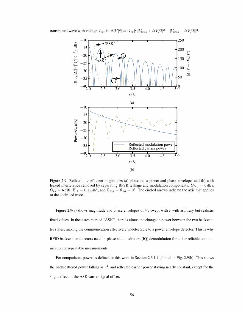
transmitted wave with voltage Vtx, is |∆|V |2| = |Vtx|2||Vleak +∆V/2|2 − |Vleak −∆V/2||2.
"PSK"
"ASK"
(a)
(b)
Figure 2.9: Reflection coefficient magnitudes (a) plotted as a power and phase envelope, and (b) with
leaked interference removed by separating BPSK leakage and modulation components. Gtag = 0 dBi,
Grd = 6 dBi, E11 = 0.1∠45, and Φtag = Φrd = 0. The circled arrows indicate the axis that applies
to the encircled trace.
Figure 2.9(a) shows magnitude and phase envelopes of V , swept with r with arbitrary but realistic
fixed values. In the states marked “ASK”, there is almost no change in power between the two backscat-
ter states, making the communication effectively undetectable to a power envelope detector. This is why
RFID backscatter detectors need in-phase and quadrature (IQ) demodulation for either reliable commu-
nication or repeatable measurements.
For comparison, power as defined in this work in Section 2.3.1 is plotted in Fig. 2.9(b). This shows
the backscattered power falling as r4, and reflected carrier power staying nearly constant, except for the
slight effect of the ASK carrier signal offset.
56

2.3.6 Power Conservation at Network Interfaces
A valid model will ensure energy is conserved. In steady state, this is equivalent to conservation of power.
This is also important in link analysis, which needs power quantities that can be directly compared.
Passive UHF RFID tags use ASK load modulation, because the “match” state can absorb and rectify
the incident carrier as a power supply. It is well-known that the penalty in use of ASK (which is required
for binary-modulated harvesting systems) instead of BPSK load modulation is a factor of 4 in power
[77]. For ASK load modulation switched according to EPC C1G2 encoding schemes, an ideal rectifier
could absorb half of the incident power. This leaves a quarter of the incident power. Where did it go?
The key to answering this question is to follow all of the power components that we have defined
already: transmission loss, the backscattered modulation component, the leaked carrier, and power de-
livered into the tag load.
Z0-matched Case
Consider a well-matched monostatic interrogator attached directly to a modulator (E11 = E33 =
0, E31 = E13 = 1). Equations (2.9), (2.25), and (2.25) combine to give
Pbs =|∆V |24Z0
= Ptx|∆ρL|2
4. (2.43)
The actual carrier power as measured on a spectrum analyzer is
Pcw =|V |2Z0
= Ptx|ρL|2, (2.44)
where ρL is the average reflection coefficient of the tag loads. This is zero when the average ρL (and
therefore the average baseband voltage V ) is equal to zero. As such, it is not the same as “leaked power”
for ASK.
It has been identified as distinct from “structural-mode” antenna scattering [78] (discussed in the
Chapter 4).
Some power is also absorbed by the modulator loads, depending on mismatch and the duty cycle
spent in each state. For ASK, this is by design. For ρL = 0, 1 loads at 50% duty cycle, the loads
absorb all of the power half of the time, or half of the incident power.
57

ASK loads BPSK loads
Load states ρL1,L2 0,1 -1,1
Reflected ASK Pbs Ptx/2 2Ptx (!)
Reflected carrier Pcw Ptx/4 0
Absorbed power PL Ptx/2 0
Total (ASK definition) 1.25Ptx (!) 2Ptx (!)
(a) with ASK-defined modulation
ASK loads BPSK loads
Load states ρL1,L2 0,1 -1,1
Reflected BPSK Pbs Ptx/4 Ptx
Reflected carrier Pcw Ptx/4 0
Absorbed power PL Ptx/2 0
Total (BPSK definition) Ptx Ptx
(b) with BPSK-defined modulation
Table 2.1: Power flow for a Z0-matched interrogator connected to a backscatter modulator
Now let the load modulation be realized as ideal ASK or BPSK load modulation. Corresponding
power quantities are summarized in Table 2.1, for each of the ASK and BPSK backscattered power
definitions.
The results for ASK modulation definition with BPSK loads are strange. For BPSK tag loads, it
appears possible for the interrogator to receive twice as much modulation power as it transmit. This
clearly violates conservation of energy. What happened? The ASK-defined modulation power assumes
a carrier component equal to the modulation component, but there is no reflected continuous-wave (CW)
power component — the average of ρL is 0. This could be remedied somewhat with leaked power
definition by subtracting the “leaked” carrier component, but this needs a nonphysical negative leaked
carrier power.
The BPSK definition, in contrast, results in power levels that conserve energy.
General Case of BPSK Passivity
In fact, RFID backscatter modulation power is conserved at any interface with the BPSK model.
Consider the sum of all power absorbed at an interface in a backscatter modulation system:
∑
P = Pbs + Pcw + PL1 + PL2. (2.45)
The two terms on the left are power reflected back to the generator and absorbed, and PL1,L2 are the
58

power delivered into each modulation load. The power wave reflection coefficient at this interface
switches between ρL1 and ρL2. From the theory developed in this chapter, the total of all absorbed
power is
∑
P =1
4|ρL2 − ρL1|2Ptx +
1
4|ρL2 + ρL1|2Ptx +
1
2(1− |ρL1|2)Ptx
1
2(1− |ρL2|2)Ptx.
=1
4[|ρL2|2 + |ρL1|2 − 2|ρL2ρL1| cos (∠ρL2 − ∠ρL1)]Ptx
+1
4[|ρL2|2 + |ρL1|2 + 2|ρL2ρL1| cos (∠ρL2 − ∠ρL1)]Ptx
+ 1− 1
2[|ρL1|2 + |ρL1|2]Ptx
=Ptx
(2.46)
As expected, the sum of dissipated power equals the sum of power input into the system. This is fully
general for any passive backscatter modulation load attached to a linear network.
2.4 Summary
Backscatter power is not explicitly derived in terms of measurable signals by standards or other technical
technical literature. Passive UHF RFID encoding makes BPSK independent of the carrier, simplifying
spectral analysis and ensuring that energy is conserved at all reference points for arbitrary passive tag
modulation loads.
Digitally modulated backscatter can be analyzed as either ASK or BPSK plus an appropriate base-
band DC offset. Defining the signal as BPSK, and not as ASK as is effectively chosen in current test
standards [41], has several advantages that arise from orthogonality with carrier frequency. Defining
FM0- or Miller-modulated backscatter as BPSK is spectrally separate from the carrier, and can be mea-
sured in the frequency domain. Finally, expressions for power conservation are straightforward with this
definition because the modulation power does not incorporate energy that is redundant with the leaked
carrier, which does not even exist for ideal PSK load modulation.
The important limiting assumptions of the signal power defined in this chapter and used in this thesis
are as follows:
(1) Switching transients in V must decay rapidly enough to allow two clearly defined states. This
59

requires slow frequency and low dispersion in propagation and matching relative to the signal
bandwidth.
(2) 50% duty cycle (as in the encoding of the EPC C1G2 and ISO 18000-6C RFID standards).
(3) The bandwidth of the baseband signal F [Vbs(t)](f) must be less than twice the carrier, 2πfc.
The remainder of this thesis assumes that these are true.
Material in this chapter originated in the following peer-reviewed publications by the author:
D.G. Kuester, D.R. Novotny, J.R. Guerrieri, Z. Popovic, “Baseband Voltage and Power in Load-
Modulated Digital Backscatter,” IEEE Antennas and Wireless Propagation Lett., accepted for pub-
lication.
60

Chapter 3
Passive Backscatter Link Power
Characterization
Milou: «Tintin! Es-tu mort? Dis-moi oui ou non,
mais reponds-moi! »
Snowy: “Tintin! Are you dead? Say yes or no but
answer me!”
Hergé, Tintin au pays des Soviets (1930)
The fundamental goal of link modeling is to estimate signal and noise levels to forecast wireless
communication quality. This can help application engineers identify and specify performance parame-
ters, and weigh cost against performance in hardware selection or design.
This is not a new idea in either digital communication in general [83, p. 118] or passive RFID [84, 85].
A link model with receiver SNR or SIR performance information can lead to estimates of data error rates
like bit error rate (BER) or frame error rate (FER) or their complimentary success rates. The coverage of
communication, which is often discussed in wide area systems like cellular networks, is the proportion
of a physical area or volume in which the communication error rate or success rate is acceptable.
Communication between readers and tags in all modern RFID systems is bi-directional and therefore
employs two different links. Both links need low error rates for reliable communication. Passive UHF
61

Forward link parameters Return link parameters
Reader hardware: Transmit power Sensitivity
(up to 30 dBm) (-85 dBm to -60 dBm)
Environment:
Reader to tag range (up to about 15 m)
Reader antenna gain pattern (up to 6 dBi at full power)
Reader antenna match losses (typically negligible)
Polarization (typ. 0 dB loss to 3 dB loss)
Tag hardware Sensitivity Differential RCS
(about -10 dBm to -20 dBm) (typically at least 0.005 m2)
Table 3.1: Typical link power parameters in free-space analysis
RFID is composed of a forward link (downlink) the reader-to-tag transmission, and return link (uplink),
the tag-to-reader backscatter. In the idealized free field (far field propagation in free space), these links
depend on the parameters are summarized in Table 3.1 [86], which themselves depend on frequency and
sometimes power. It is often assumed that the forward link limits overall communication reliability, but
we will show in Chapter 6 that this is not always true with modern commercial hardware.
Despite the large number of variables in these links, passive UHF RFID literature typically quotes
link performance as a single “tag read range” number (sometimes as a function of frequency). The term
is not standardized, but seems to suggest the maximum separation between reader and tag antennas at
some acceptable error rate. A subset of the measurement details are sometimes given that may hint at
when the metric applies. Usually, however, it is difficult to identify the radio environment where tag read
range applies, and even more difficult to use it to predict behavior in other environments.
This chapter investigates link operation with network theory, with the goal of leveraging redundancy
between losses in each link to better understand and predict the behavior of the return link. Tag BPSK
radar cross section and sensitivity that characterize behavior conveniently in free space emerge as special
cases of this analysis. The final result, however, is an alternative to radar cross section for bounding
backscattered power in monostatic or “quasi-monostatic” return links with passive tags. This parameter
gives a deterministic lower bound to backscattered power as a function of tag tuning in any environment.
62

Figure 3.1: Linearized S-parameter model of reader and tag signaling. In return modulation, the tag chip
switches between ρL,R (impedances ZL,R). The tag antenna, loaded slightly by the reader, presents ρ3(impedance Z3) to the chip. Backscatter at ports 1 and 2 is produced by interaction between the tag
antenna and the switching chip load.
3.1 Reader-Loaded Link Model
A network model of interaction between a reader and tag is illustrated in Fig. 3.1, following [43] and
[46]. The S-parameter network E contains all transmission effects between reader ports and a tag chip,
including cables, antennas, and propagation effects. Ports 1 and 2 of E are attached to the monostatic or
bistatic reader. Port 3 is the interface between the tag’s chip and antenna. The reader transmits into port
1 or 2; each is assumed not to load the other.
We adopt a change of variables compared to the previous chapter for the special case of passive tags:
the power harvesting chip impedance state is ZL1 → ZL, and the reflective modulation chip impedance
state is ZL2 → ZR. Realistic values are on the order of ZL ≈ (15 − j150)Ω, ZR ≈ (12.5 − j100)Ω
[87], and Z3 ≈ Z∗L. Reader ports and antennas are usually designed to match 50Ω.
3.2 The Forward Link as a Microwave Network
3.2.1 Propagation Power and Loss
Available transmit power from the reader (Ptx) is related to S-parameter traveling waves incident into
either port (a1,2) with [56]
63

Ptx =|a1,2|2
1− |ρI1,I2|2. (3.1)
Likewise, available power from the tag antenna, P3, is related to the corresponding scattered pseudowave
b3 as
P3 =|b3|2
1− |ρ3|2, (3.2)
where ρ3 is E33 loaded through E by the reader. The exact expression for ρ3 is long and uninformative,
but ρ3 ≈ E33 if the reader is well matched or E transmission coefficients are small. The proportion of
available transmit power that is available out of the tag antenna is the available power gain [62, p. 539],
P3
Ptx=
1
Ltx= |E31,32|2
1− |ρI1,I2|2|1− E11,22ρI1,I2|2(1− |ρ3|2)
. (3.3)
Its inverse, Ltx, is the transmission loss. Current systems can to turn on well-matched tags with up to
about 45 dB of loss.
3.2.2 Tag Turn-on as a Nonlinear Operating Point
A well-matched state-of-the-art tag chip must absorb on the order of PL0 = −15 dBm to turn on. Am-
bient noise power is much smaller in typical environments, so turn-on is a threshold effect that depends
on absolute PL, not power relative to noise (SNR). As a result, there is a sharply-defined power avail-
able from the tag antenna, P30, where the tag load is at the turn-on threshold. Any P3 can be expressed
relative to this as P3 = pP30. Excess power p can be interpreted as “power level relative to turn-on.” If
it is expressed in dB, it can be read “dB above turn-on.”
The BER distribution as a function of P3 is closely approximated as a step function, which is de-
terministic with input power. Interference effects in this link are limited: would-be “interferers” may
instead help to power the tag [40]. This is in sharp contrast with an ideal AWGN-limited channels, for
which the BER distribution is the error function [84]. The AWGN frame failure rate requires the success
of many bits in sequence, and is therefore poorer but still a random variable.
A sensitive reader can remotely detect whether a tag is on by detecting backscattered power, Pbs, at
64

some power level:
Pbs = 0, for Ptx < Ptx0, (3.4)
where Ptx0 is the minimum power to turn on. All terms on the right of (3.3) are linear, and thus indepen-
dent of operating point, P3/Ptx = P30/Ptx0. Therefore,
p =Ptx
Ptx0=
P3
P30. (3.5)
In other words, the operating point has the same meaning either at the reader ports or inside the tag.
This concept is exploited (though not explained) in ISO 18047-6 [41], prescribing σ∆ measurements
at p = 120% (0.8 dB). Because p permits wireless insight into power levels inside the tag, it is the basis
for linearity test and analysis in this thesis.
3.2.3 Power Delivery to the Tag Chip Load
A passive UHF RFID chip has the power harvesting load impedance ZL except at 50% duty cycle during
tag-to-reader modulation, to maximize time-averaged rectified power. It is the convention of this thesis
that power delivery is defined for the chip in its power harvesting impedance ZL, and not in reflective
state ZR.
Available power from the antenna (P3) is related to power delivered to the tag chip (PL) as
PL =P3ηL
=Ptx
LtxηL.
(3.6)
This defines 0 ≤ ηL ≤ 1 as the match efficiency between the tag antenna and the tag chip.
At the turn-on operating point, we define the chip sensitivity PL0:
PL0 = P30ηL0. (3.7)
Nonlinear Matching Effects
Physical tag loads are realized as nonlinear diodes or transistors, so their input impedances at the carrier
frequency vary with input power (through p) and the tag antenna impedance at harmonics of the carrier
65

nfc (n = 0, 1, 2, 3, ...). Propagating this dependence into (1.21) gives an unwieldy result for ηL:
ηL(p, Z3(nfc)) =(1− |ρ3|2)(1− |ρL(p, Z3(nfc))|2)
|1− ρ3ρL(p, Z3(nfc))|2
=4ReZL(p, Z3(nfc))ReZ3
|ZL(p, Z3(nfc)) + Z3|2.
(3.8)
If the Z3 and ZL are conjugate-matched at the fundamental, ηL = 1 and all power available at the antenna
terminals is delivered from the antenna into the chip. Ohmic losses inside the antenna are included as
part of the transmission network.
This efficiency is different from the RF-to-DC conversion efficiency in rectifier design. For example,
a rectifier could be a good linearized conjugate match ZL = Z∗3 , but any additional loss inside the
rectifier will reduce ηL.
Parasitic Packaging Effects
Equation (3.8) is meant to predict power absorption performance from impedances that can be predicted
in advance by measurement, simulation, or theory. Unfortunately, the bond between the tag chip and
antenna introduces parasitic effects that are likely to contribute to differences between measurement
test fixtures, simulations, and the final bonded tag [88, 89]. The convention in this work, illustrated in
Fig. 3.2, is to incorporate these into the chip impedances ZL and ZR. This way, Z3 can be thought of
as “fixed.” Both ZL and ZR already depend on Z3 because of their nonlinearity, so incorporating the
correction for parasitics simply changes this existing dependence.
Time Dependence
So far, ZL and PL0 have been tacitly assumed to be time-invariant at “fixed” reader transmit power levels
on the scale of many carrier frequencies. Sadly, this is not true. The time-dependence of these parameters
is a large and complicated problem that could be its own thesis chapter, as in in [26, pp. 18-22]. Here,
time dependence will be addressed qualitatively enough to understand link performance concerns.
One reason is that the reader transmit power is not really fixed. By definition, the ASK reader-to-tag
modulation varies the transmit power of the reader. This variation toggles the power supply broadcast to
the tags, which must have a small DC buffer capacitor to maintain supply during baseband “off” cycles.
66

Figure 3.2: The network interface between a tag antenna and chip is not well-defined. Impedances from
(a) simulations or measurements in a test fixture do not describe (b) additional circuit effects introduced
by bonding the chip to the antenna. The convention in this work is to incorporate these additional effects
into the chip impedances.
Figure 3.3: The DC supply voltage within an EPC C1G2/ISO 18000-6C tag during a communication
round [90].
67

Solving this problem by increasing the buffer capacitance increases chip area and cost, and is also limited
by the charging time permitted by the protocol. At best, this scheme “averages” DC supply across the
order of 10 µs, resulting in DC supply voltage droop and less available DC power. This is illustrated as
the first droop in Fig. 3.3, settling to about half of the CW supply voltage. If there is too much voltage
droop, the tag chip turns off and fails to respond to the reader.
The act of shorting the chip’s input impedance during return-link backscatter modulation also effec-
tively switches the tag power supply on and off, even though the reader is transmitting fixed CW during
this period. The chip’s DC buffer capacitance helps again, but has similar problems as the forward link.
This is visible as the shorter droop labeled “chip’s reply” in Fig. 3.3.
The DC load presented by the tag’s digital circuitry is also not constant. The rectifier is far from an
ideal voltage source, and may droop when the load draws too much current. The tag must use power
during both links: 1) decoding requests from the reader, 2) accessing its memory, 3) processing a reply,
and perhaps performing extended functions like sensing. If the load exceeds the sourcing capability
of the rectifier at any stage in communication, the tag might return an incomplete or invalid response
that prevents valid communication. Memory write operations, for example, use more power and thus
correspond with poorer sensitivity for all commercial passive chips, e.g., [91, 92].
Further, ZL itself varies with the DC load. The detailed nature of this dependence is determined by
the rectifier topology; the charge pumps used in RFID involve trade-offs between efficiency and isolation
between the DC load and RF input impedances [93, p. 31]. Time-varying ZL implies time-varying ηL as
well, so an “optimal” power harvesting match during forward-link modulation can in principle be quite
different if the loading is not carefully spread out. Fortunately, at least for some commercial chips, these
effects have been observed to be slight [87].
If we are given only a fully integrated tag, these effects are extremely difficult to measure or quantify.
They do help identify factors that may affect chip sensitivity PL0:
(1) Signal encoding parameters in both links: 1) symbol rate, 2) timing, 3) modulation depth, etc.
These factors have been shown to affect PL0 by less than 0.25 dB [94].
(2) Data content: a) singulation vs. memory read vs. memory write, b) how much data is sent, c) the
68

extent of processing required.
These data-dependent parameters are much more complicated to predict than those listed in (3.8), but
must be measured for complete tests.
3.3 Return Link Loss and Efficiency
3.3.1 Modulation Efficiency
The main circuit performance parameter inside the tag characterizes the modulation power accepted by
the tag antenna as a fraction of the incident carrier power available into the tag chip. This takes exactly
the same form as (2.33), but is evaluated with ρI1 → ρ3, ρ1(ρL1) → ρL, and ρ1(ρL2) → ρR:
ηmod(p, Z3(nfc), reader command)
=
(
1− |ρ3|2|1− ρ3ρL(p, ρ3(nfc))||1− ρ3ρR(p)|
)2
|ρR(p)− ρL(p, Z3(nfc))|2
=
(
Re(Z3)
|Z3 + ZR(p)||Z3 + ZL(p, Z3(nfc))|
)2
|ZR(p)− ZL(p, Z3(nfc))|2
=1
4|ρR(p)− ρL(p, Z3(nfc))|2.
(3.9)
To include this chapter’s nonlinear compression effects, this expression depends on p. The expression is
identical for both monostatic and bistatic operation. For passive ρL,R, modulation efficiency is bounded
by 0 ≤ ηmod ≤ (1 +√1− ηL)
2.
The definition of “modulation efficiency” in (3.9) specifically relates backscattered BPSK modulation
to the available incident carrier power. Use of BPSK has the specific advantages that were discussed in
Chapter 2. Previous work that uses this type of term does not explicitly state the type of reflected
modulation, but it can be inferred from the normalization factor. The normalization as |ρR − ρL|2/4
given here corresponds with BPSK, as in [71, 95]. Normalization as |ρR − ρL|2/2 is reflected ASK,
which is used by [44]. Many others use |ρR − ρL|2 [43]; these come from [69, p. 31] by way of [77].
The dependence on the antenna properties shows that this backscatter is produced not by the switch-
ing tag chip impedance, but by its interaction with the antenna as a circuit element. Just as in the forward
link, the tag antenna is still assumed linear, even though the interactions between it and the tag chip are
69

not.
3.3.2 Link Power and Loss
Monostatic backscatter presented at a reader after passing through the environment are already given in
terms of pseudowave scattering parameters (2.6). These scattering parameters are related to backscatter
power absorbed by the reader in (2.33), tag modulation power efficiency defined in (3.9), and the trans-
mission path loss is defined in (3.3). Combining all of these equations lets us decompose the monostatic
link budget into efficiencies and link losses,
Pbs
Ptx
ηtxηrx
=ηmod(p)
L2tx
(monostatic through port 1). (3.10)
The factor of ηtx/ηrx will be addressed in the next subsection.
The bistatic expression for this is derived much the same way, except substituting power expressions
into (2.2):
Pbs
Ptx
ηtxηrx
=ηmod(p)
LtxLrx(bistatic through ports 1 and 2). (3.11)
The difference here are
(1) L2tx is split into separate path losses that correspond to the bistatic transmit and receive paths
between the reader and tag, and
(2) ηtx and ηrx now refer to ports 1 and 2 of the reader and environment, and their ratio becomes
much more complicated.
3.3.3 Reader Mismatch Effects on Backscatter
Let us consider the term ηtx/ηrx that falls out of the link derivation but does not appear elsewhere in the
literature. In the monostatic case, evaluating each match efficiency expression reduces to
ηtxηrx
=
( |(1− ρI1ρ1)2 − (ρI1∆ρ1)
2|2|1− E11ρI1|4
)2
, (3.12)
which is very ungainly, even though many terms in transmit match efficiency, 0 ≤ ηtx ≤ 1, and receive
efficiency, 0 ≤ ηrx ≤ 1 have cancelled. The dependence on ∆ρ1 is particularly inconvenient because it is
70

Figure 3.4: Absolute worst-case upper and lower bounds for ηtx/ηrx when |E11|2 < −5 dB for the
values of |ρI1|2 shown. Realistic “far-field” values of path loss are above approximately 15 dB.
unknown in practical operation. These are the matching terms in the forward and return link expressions
that do not cancel. This is because the forward link available power model presents the environment not
loaded by the tag; in contrast, the return link environment model presents the time-averaged reflection
coefficient of the environment loaded by the tag, and effects of multiple reflections of the modulation
wave.
Under certain conditions, like the approximation of (2.34), this term becomes negligible:
(1) when the reader is matched to Z0 so that |ρI1| = 0, or
(2) when both a) the tag loads do not significantly load the reader antenna, so that E11 ≈ ρ1, and b)
|ρI1∆ρ1|2 ≪ |1− ρI1ρ1|2, or
(3) both (1) and (2).
One way to achieve this and make ηtx/ηrx vanish is to define the reference impedance Z0 to be the same
as the (real-valued) input impedance of the reader, so that by definition ρI1 = 0.
Figure 3.4 illustrates absolute maximum and minimum bounds for ηtx/ηrx for return loss in ρI1
and E11 greater than 5 dB. These occur when all terms are entirely real-valued, adding exactly in phase
or out of phase. Effects from ρ1 are strongest when reflections from the modulator have a strong car-
rier frequency component, and effects of ∆ρ1 are strongest when reflections from the modulator have
strong sideband components. The illustrated bounds assume the nonphysically bad case of the modulator
71

Figure 3.5: Definition of antenna pattern orientations θ and φ and polarization unit vector u, following
[96, p. 33]. The example polarization is specific to linear-polarized antennas like the dipole shown.
reflecting all incident power as both carrier and modulation in order to guarantee conservative bounds.
3.4 Free Field Tag Performance Characterization
Standard free-space forward and return link metrics now derive trivially by substituting free space power
loss for L via the Friis transmission equation. These exist elsewhere in the literature, but details in the
preceding link and signal discussion connect with broader wireless communication concepts. These will
help us identify the important parameters that affect backscattered power received by the reader within
this free space case. These depend on the reader and tag antenna orientations illustrated in Figs. 3.5 and
3.6.
3.4.1 Power harvesting performance: sensitivity
With the terms defined so far, the Friis transmission equation for power loss in far field, free space (“free
field”) propagation is [96, p. 95]
P3
Ptx=
1
L=
(
λ
4πr
)2
G3(θtx, φtx)Grx(θ3, φ3)|u3 · utx|2. (3.13)
The separation between the reader and tag antennas is r and the wavelength in the propagating medium
is λ = c/f . The reader and tag antennas have total gain Gtx and G3, with corresponding unit polar-
ization vectors u3 and utx. The corresponding orientations of these antennas are (θtx,φtx,∠utx) and
72
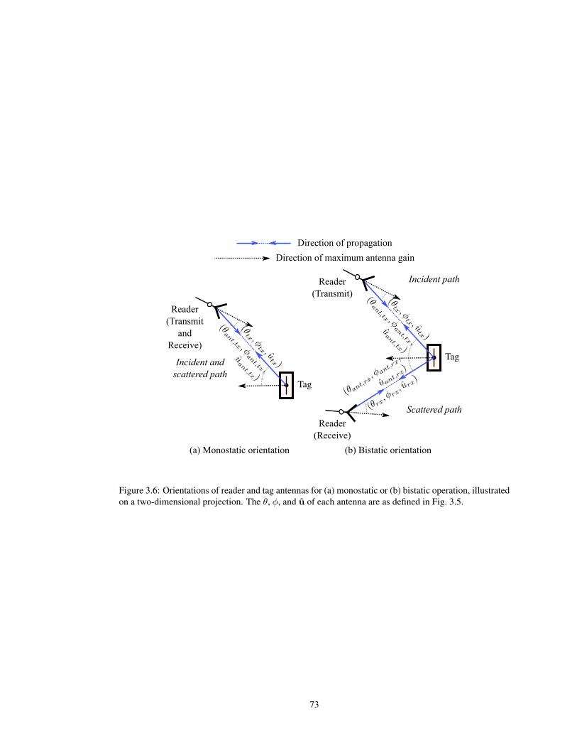
Direction of propagationDirection of maximum antenna gain
Incident andscattered path
Reader(Transmit
and Receive)
Incident path
Scattered path
Reader(Transmit)
Reader(Receive)
(a) Monostatic orientation (b) Bistatic orientation
Figure 3.6: Orientations of reader and tag antennas for (a) monostatic or (b) bistatic operation, illustrated
on a two-dimensional projection. The θ, φ, and u of each antenna are as defined in Fig. 3.5.
73

(θ3,φ3,∠u3).
Use of this expression in this form is problematic given the tight integration between the tag antenna
and chip. We can work around this by combining P3 and G3 terms into the plane wave power density, W ,
[38, 39, 97]. Other authors have also related this to the electric field. The only operating characteristic
we can identify externally is the plane wave impinging on the tag at its turn-on threshold, W |p=1 = W0:
W0(f, θ3, φ3, u3) = P30(f, Z3)4π
λ2G3(f, θ3, φ3). (3.14)
This encapsulates only the parameters of the tag, except for the dependence on the incident wave polar-
ization through utx. Like P3, W0 varies with the power consumption of the tag.
A well-matched reader-antenna system can excite this power density by transmitting Ptx0, such that
W0
Ptx0=
Grd
4πr2|u3 · utx|2, (3.15)
where Grd is the reader antenna gain toward the tag, and r is the range between the reader transmit and
tag antennas.
3.4.2 Backscatter Performance: BPSK Radar Cross-Section
Bistatic readers use two separate “transmission” paths with losses Ltx and Lrx, that correspond to the
incident and scattered waves. These have different antenna separations, rtx and rrx, different reader
antennas with gain Gtx(θtx, φtx) and Grx(θrx, φrx), different incident and scattered tag orientations,
(θant,tx, φant,tx) and (θant,rx, φant,rx), and corresponding unit polarization vectors for each. Substitut-
ing the Friis equation with these parameters into (3.11) gives
Pbs
Ptx
ηtxηrx
=ηmod(p)
L2= ηmod(p)
(
λ
4πr
)4
Gtx(θtx, φtx)G3(θant,tx, φant,tx)|uant,tx · utx|2.
×Grx(θrx, φrx)G3(θant,rx, φant,rx)|uant,rx · urx|2
(3.16)
The author assures concerned members of the public that this thesis will not make a habit out unwieldy
equations like this.
74

Like P3 and G3 in the forward link, the ηmod and G3 terms are not suited for direct measurement
once a tag is integrated. Just as we encapsulated terms into W0 in the forward link, we can collect these
terms together into bistatic BPSK radar cross-section,
σ∆(p, θant,tx, φant,tx,θant,rx, φant,rx, uant,rx, uant,rx)
=λ2
4πG3(θant,tx, φant,tx)G3(θant,rx, φant,rx)|uant,rx · urx|2ηmod(p),
(3.17)
following the original notation of [69]. This includes the effects of polarization mismatch specified only
in the scattered (i.e., receive path) direction according to the definition of [98, p. 31]. This differs by the
factor of 4 through our definition of ηmod in (3.9) compared to the quantity known as “differential radar
cross-section (RCS)” [42, 99], “∆RCS” [41, 44], “RCS” [10, p. 322] [43], or “echo area,” [69].
Substituting σ∆ into (3.16) gives the bistatic radar equation,
Pbs
Ptx
ηtxηrx
= Gtx(θtx, φtx)Grx(θrx, φrx)σ∆(θ3, φ3)λ2
(4π)3r2txr2rx
|uant,tx · utx|2. (3.18)
Like the convention of (3.15), this includes only the polarization loss of the incident plane wave, to leave
the RCS definition according to IEEE standard terminology.
The monostatic case is somewhat simpler, because there is only one path. There is therefore only one
relavant reader antenna orientation (θtx, φtx, utx) = (θrx, φrx, urx), and one tag antenna orientation,
(θant,tx, φant,tx, uant,tx) = (θant,rx, φant,rx, uant,rx) = (θ3, φ3, u3). Inserting the Friis equation into
into L in (3.10) gives:
Pbs
Ptx=
ηmod
L2= ηmod
[
(
λ
4πr
)2
Gtx(θtx, φtx)G3(θ3, φ3)|u3 · utx|2]2
. (3.19)
Substituting (3.21) back into (3.19) gives the monostatic radar equation,
Pbs
Ptx
ηtxηrx
=G2
tx(θtx, φtx)λ2σ∆(θ3, φ3)
(4π)3r4|u3 · utx|2, (3.20)
with the monostatic BPSK radar cross section:
σ∆(p, θ3, φ3, utx, u3) =λ2
4πG3(θ3, φ3)
2|u3 · utx|2ηmod(p). (3.21)
3.4.3 Backscatter Performance: Carrier Radar Cross-Section
A central theme of Chapter 2 was that useful BPSK modulation received by the reader is independent of
the received carrier wave, except for effects on matching (neglecting desensitization effects). Reflections
75

Typical leaked power Network Radar
Reflection source (normalized to Ptx) parameter parameter
Reader antenna mismatch (monostatic operation) -25 dB to -15 dB E N/A
Reader antenna leakage (bistatic operation) -40 dB to -15 dB E N/A
Tag antenna structure ∝ 1/r4 by (3.20),(3.18) E σcw
Tag antenna loads ∝ 1/r4 |ρR + ρL|/4 σcw
Table 3.2: Sources of carrier leakage for systems operating in free space
from the tag antenna at the carrier frequency are therefore second-order effects in realistic operation,
and sometimes negligible. This view is also supported by prior literature (e.g., [70]). Unfortunately,
confusion about the effects of antenna scattering at the carrier has filled the literature with questionable
design and measurement practices.
Potential sources of carrier reflections are listed in Table 3.2 (for the free-space domain in which the
radar equation is valid). Each source is listed with the corresponding parameter that encapsulates it in
the network model or the radar model.
A key difference between the representation of these reflections in the model is listed as from the
antenna structure reflection, sometimes called “structural-mode” antenna reflections. This is reflection
from the tag antenna structure caused by currents excited on the antenna that do not interact with the tag
chip. In the network model, this is included as part of the environment, because it is between the reader
antenna and tag antenna reference planes. In the radar model, which regards the antennas as black boxes
interacting based on geometric position, this effect must be included in the RCS of the target, to preserve
the free space assumptions around it.
One approach to analysis of loaded antennas is proposed in Green’s 1963 thesis. He defines a power-
wave reflection coefficient, A, that is the equivalent antenna load that would result in structural-mode
reflections in a given orientation. It is related to the structural mode component of RCS at the carrier
frequency, σs, through:
σs(p, θant,tx, φant,tx,θant,rx, φant,rx, uant,rx, uant,rx)
=λ2
4πG3(θant,tx, φant,tx)G3(θant,rx, φant,rx)|uant,rx · urx|2
× |A(θant,tx, φant,tx, θant,rx, φant,rx, ·urx)|2.
(3.22)
Expressing the full orientation and gain dependences here has made it nearly unreadable, but underscores
76

Antenna type |A|Pyramidal standard gain horn (E-plane) 0.2
λ/2 dipole 1
λ/2 dipole (λ/2 behind5
a λ× λ PEC plate)
Table 3.3: Examples of co-polarized boresight |A| (based on [96, pp. 103-104])
the complexity underlying the simplified free space equations. This is equation (44) in [69, p. 40] ex-
panded into the more general bistatic case and adapted to fit the notation of this thesis. Structural-mode
reflections (via A) have orientation dependence separate from antenna mode reflections (via G3), so A
depends on orientation separately from G3.
A few examples of antennas and corresponding co-polarized broadside |A| are listed in Table 3.3.
The horn has the weakest structural-mode scattering component, so for large antenna load mismatch, the
antenna mode scattering is likely to dominate. The value A ≈ 1 is taken as almost axiomatic for a λ/2
dipole (but it is not exact). If a perfectly conducting λ × λ plate is placed behind this dipole, then by
image theory the dipole gain doubles, and so the antenna-mode RCS quadruples. The sheet itself is a
reflector, with an RCS component σs = 4πλ2 in phase with that of the dipole. Solving for |A| gives the
indicated value; if the area of the sheet is increased toward infinity, |A| approaches infinity at the same
rate.
If the antenna load is fixed (not switching) but mismatched, there are both structural- and antenna-
mode reflections corresponding to the power wave reflection coefficient of the load, ρ. The corresponding
total antenna RCS, σ, is
σ(p, θant,tx, φant,tx,θant,rx, φant,rx, uant,rx, uant,rx)
=λ2
4πG3(θant,tx, φant,tx)G3(θant,rx, φant,rx)|uant,rx · urx|2
× |A(θant,tx, φant,tx, θant,rx, φant,rx, ·urx)− ρ|2.
(3.23)
Since |A| can become very large but |ρ| ≤ 1, it is often true that the structural-mode reflection component
is larger than the antenna-mode component. This is particularly significant when mechanical mounts,
non-radiating feed structures, or large reflectors are taken into account. An antenna for which A = ρ
in a desired direction is called a “minimum scattering” antenna, for σ = 0. This is often taken to be
77

a reasonable approximation for dipole-type tag antennas. Thus, there are no reflections for an antenna
with A = 1 and a conjugate-matched load.
The parameter is referenced to the same phase and magnitude as the chip loading the antenna. By
adding the “effective” carrier reflection coefficient in the tag, the bistatic RCS corresponding to the total
reflected power at the carrier, σcw, is
σcw(p, θant,tx, φant,tx,θant,rx, φant,rx, uant,rx, uant,rx)
=λ2
4πG3(θant,tx, φant,tx)G3(θant,rx, φant,rx)|uant,rx · urx|2
×∣
∣
∣
∣
A(θant,tx, φant,tx, θant,rx, φant,rx, ·urx) +ρR + ρL
2
∣
∣
∣
∣
2
.
(3.24)
Still, despite the efforts invested in this discussion, application of σcw and the radar equation to
passive UHF RFID is not useful in far-field operation. First, determining A other than by assumption is
difficult and complicated. Second, in far-field operation where tag responses are weakest, the effect of
tag scattering on matching is likely to be negligible, so the result is of little value. Third, propagation
reflections in industrial indoor environments are likely to be much larger than the reflection from the
antenna, making it even more negligible.
3.4.4 Backscatter Performance: Other tag RCS models in the literature
The “useful” backscatter is now shown exhaustively to be contained in BPSK modulated sidebands, and
characterized and applied in free space through σ∆. The interfering but much less significant tag carrier
frequency reflections are established in σcw. Importantly, the structural scattering component exclusively
affects the carrier frequency power through σcw.
In recent years, unfortunately, confused applications of older work [69, 100] have become increas-
ingly common. The definition of σ∆ in this work agrees with others in the literature [43, 69, 71, 77,
101], except the factor of 4 ηmod caused by our definition of BPSK modulation power.
Some previous work defines tag response RCS parameters which do include A, thus including the
interfering carrier frequency signal as a part of the characterized tag response. Several works propose
78

the following model for differential RCS [78, 79, 102–104]:
“Differential RCS” =λ2
4πG3(θant,tx, φant,tx)G3(θant,rx, φant,rx)|uant,rx · urx|2
× |A(θant,tx, φant,tx, θant,rx, φant,rx, ·urx) + ρ|2.(3.25)
This is the same as the total carrier frequency RCS at fixed frequency of (3.23)! Reflected power repre-
sented by this RCS does not contain any communicated data, so it is difficult to understand how it could
will be useful in predicting link performance.
In other recent work, [105] arrives at the differential RCS of [77], but unfortunately conflates this
with the assumption that it is only valid for minimum scattering tag antennas. This leads to further
confusion and the assertion that more generally differential RCS in general varies with A according to
(3.25).
The notation “∆σ” is sometimes used (as in [41, 106]) instead of ∆σ (as in [69]), causing more
confusion. An early version of ISO test standard [41] and many authors [80, 81, 107–110] misunderstand
the intent of this as subtraction between two real-valued power quantities. This causes the power envelope
interference problems discussed in Section 2.3.5, where tag responses are invisible for certain reader-to-
tag antenna separations.
The “alternate models” in these works form the basis for design practices that seek to optimize tag
design by careful selection of A. Unfortunately, as this section has demonstrated, there is no effect of A
on σ∆. Reflections caused by large A have only the second-order effect of changing the self-interfering
leaked carrier and some mismatch for the modulation at the reader, but only if the tag antenna is very
large or very close to the reader antenna.
3.5 A Tag Backscatter Metric for Arbitrary Propagation Loss
The free field expressions for P3 and Pbs are simple only in the sense that they can be expressed as simple
products of loss terms. Unfortunately, these terms beget a huge number of degrees of freedom: 9 degrees
for transmission and monostatic backscatter, and 16 for bistatic backscatter (mostly from the number
of combinations of different antenna orientations). Adding realistic fading effects like shadowing and
79

multipath into Pbs becomes cripplingly complicated, which may explain the lack of literature on the
subject.
When the tag is fully passive, p is clearly defined, and forward link tests can give W0 rapidly if
a calibrated and adjustable field or plane wave source is available. There is a great deal of redundant
information in the free-space tag link behavior in the forward link through (3.15) compared to the return
link by (3.20) or (3.18): reader and antenna gains and orientations and r are shared.
The general link loss models of (3.3), (3.10), and (3.11) suggest that this extends quite generally.
Bolomey et al [43, 111] were the first to write about reciprocity between the forward link and return links
in arbitrary linear environments. This concept is powerful because it predicts tag backscatter behavior
beyond the free space domain of the radar equation.
This section extends these ideas to form a compact tag backscatter metric. This parameter, minus
discussion of linearity, matching, and the accompanying link arithmetic, was proposed in [112, 113] for
application to sensing with the tag. It is a central point of this thesis.
3.5.1 Bistatic Case
The arbitrary link loss formulations of power transmission and backscattering in equations (3.3) and
(3.11) are composed of the separate path losses Ltx and Lrx. Evaluating these losses at the turn-on
threshold Ptx0, which is valid because from our assumption the environment (through our original S-
parameter network E) has linear power response, gives
1
LtxLrx=
(
PL0
Ptx0
∣
∣
∣
∣
tx port
1
ηL0
)(
PL0
Ptx0
∣
∣
∣
∣
rx port
1
ηL0
)
=Pbs
Ptx
1
ηmod
ηtxηrx
. (3.26)
Notice that unlike the power harvesting term in the middle that is evaluated at tag turn-on, the backscatter
expression on the right is left to be evaluated at arbitrary Ptx. Expressing the receive path loss Ltx in
terms of turn-on levels and tag chip sensitivity means this expression involves the tag turn-on power that
a reader must transmit to turn on the tag chip from its receive port, Ptx0|rx port. This does not correspond
to the power level the reader is actually transmitting from this receive port; like the transmit port turn-on
level, Ptx0|tx port, this only describes what would be required to turn on the tag.
The tag chip sensitivity and the corresponding match efficiency at turn-on are independent of the
80

source of the power, so this simplifies to
1
LtxLrx=
P 2L0
(Ptx0|tx port)(Ptx0|rx port)
1
η2L0
=Pbs
Ptx
1
ηmod
ηtxηrx
. (3.27)
Rearranging Ptx terms and substituting Ptx = pPtx0 leaves a figure of merit, referred to in this work
as B for “backscatter:”
B(f, p, Z3(nf), reader command) = Ptx0|rx portPbsηrxηtx
= p
(
PL0
ηL0
)2
ηmod.
(3.28)
This is a central focus of this thesis. B is fixed exclusively by circuit parameters inside the tag, so it
depends exclusively upon the same parameters as the tag circuit efficiencies ηmod(p) and ηL0, mainly the
four listed variables (at fixed temperature and pressure). Importantly, this means it is entirely independent
of the propagation environment except through detuning of the tag antenna Z3(nf) (and potentially
other non-electrical effects like temperature and pressure). Taking the tagged object as the dominant
environmental effect on Z3(nf), B can be considered a parameter of a “tagged object.”
3.5.2 Monostatic Case
Analysis with monostatic backscatter detection proceeds in similar fashion, but with only the shared
transmit and receive signal path loss L. Just like the bistatic case, combining (3.3) at the tag turn-on
power level and (3.11) gives:
1
L2=
(
PL0
Ptx0
1
ηL0
)2
=Pbs
Ptx
1
ηmod
ηtxηrx
. (3.29)
This gives B as the exact same equation as (3.28), except that Ptx0|rx port = Ptx0|tx port.
3.5.3 Model Limitations from Underlying Assumptions
Recalling the underlying assumptions in the thesis so far, B by equation (3.28) is exact under the follow-
ing conditions:
(1) Backscatter modulation received by the reader has well-defined digital states (weak distortion).
(2) Propagation loss between reader and tag antennas is linear and causal with respect to power.
81

(3) The tag backscatter modulation is encoded as described in Chapter 2.
(4) Tag turn-on is abrupt and repeatable for Ptx ≥ Ptx0 (which has been verified to within 0.2 dB for
many tags).
These assumptions are implicit in all analysis for the remainder of this thesis. These are a subset of the
assumptions required to use the radar equation. Item (4) is particularly important, because it limits both
σ∆ and B to use with fully passive tags unless an alternate operating point can be defined besides p.
3.6 Comparison of Tag Backscatter Metrics
The free space parameters are simple applications of well-understood microwave theory. This section
poses them against B to shed some light on the much less well understood parameter.
It is important to understand that B and σ∆ are drastically different metrics. Like σ∆, larger values of
B suggest larger received Pbs. However, while σ∆ characterizes a tag in complete isolation, B describes
the tag under the condition that the environment allows turn-on. This is why B depends on PL0 and ηL0
— they limit the maximum forward-link loss and therefore the maximum monostatic backscatter loss.
One interpretation of B is as a balance between forward and return links. Increasing transmission
loss requires greater Ptx0 Because the loss is reciprocal, Pbs falls. The theory culminating in equation
(3.28) simply says that nature forces these trends in Ptx0 and Pbs to be proportionally inverse. This is
itself a very different concept than the proportional power loss when using σ∆ with the radar equation.
Combining the forward and reverse link models of (3.14) and (3.17) with W = pW0 relates σ∆ and
W0 to B,
B = PbsPtx0ηtxηrx = p
(
λ2
4π
)
W 20 σ∆. (3.30)
As expected, there is no dependence on reader or tag antenna position or orientation, which determine
L in free space. Substituting (3.14) and (3.17) for W0 and σ∆ causes G terms to cancel so that the
expression simplifies to (3.28).
Equation (3.30) allows any one of B, W0, or σ∆ to be computed from the other two. As a side benefit,
a B computed from free-space measurements of W0 and σ∆ generalizes to more arbitrary environments.
82

The two backscatter metrics differ in measurability. Chapter 4 will discuss calibration including
measurement of σ∆, but in short it requires either an anechoic test environment with a well-calibrated
interrogation antenna, or tightly controlled field generation in an environment like a gigahertz TEM cell.
Chapter 5 studies measurement of B, and finds that a testbed only requires a well-matched antenna and
a well-calibrated signal generator and measurements.
3.7 Application to Bounding Monostatic Backscatter Power
The link balance imposed by B leads to its simplest and most powerful application to link analysis: the
weakest backscattered power a monostatic reader can receive from a tag that is “on.” Since B increases
with p above turn-on, the minimum non-zero backscattered power occurs at p = 0 dB. The corresponding
minimum bound to backscattered power is
min[Pbs] (dBm) = [B|p=0 dB (dBm)2]− [Ptx (dBm)]. (3.31)
Here, “(dBm)2” is “dB relative to one square milliwatt,”
B (dBm)2 = 10 log10B (mW)2
1 (mW)2. (3.32)
Use of this unit is nonstandard, but allows min[Pbs] to be determined from B data “by inspection” with
the simple subtraction given by (3.31).
Because they are proportional, trends in B at turn-on are the same for min[Pbs] through (3.31).
For example, detuning that reduces B reduces min[Pbs] by the same amount. Likewise, measurement
uncertainty in B contributes the same uncertainty toward min[Pbs].
As a result, min[Pbs] of an assembled tag varies only with tag antenna tuning, frequency, and whether
the tag reads or writes. A link margin may be subtracted from estimates of min[Pbs] when specifying
reader sensitivity to account for detuning effects.
83

3.8 Summary
High-level analysis of the benefits and risks in use of RFID requires an understanding of what is possible
within the bounds of physics, standards, and emission regulations. Fundamental power parameters and
relationships defined in Chapter 2 enable informed discussion of device characterization and system
behavior in free space, and recent movement toward more general analysis based on network theory.
The alternative suggested in this chapter, B, is a more compact backscattered power characterization
than radar cross-section for passive systems. With this metric, system designers can find a deterministic
minimum bound to backscatter received from any passive tag under realistic fading conditions with a
trivial computation.
The material in this chapter originated in the following peer-reviewed publications by the author:
D.G. Kuester, D.R. Novotny, J.R. Guerrieri, Z. Popovic, “Simple Test and Modeling of RFID
Tag Backscatter,” IEEE Trans. on Microwave Theory and Techn., vol. 60, no. 7, July 2012, pp.
2248-2258
D.G. Kuester, D.R. Novotny, J.R. Guerrieri, “Forward and Reverse Link Constraints in UHF RFID
with Passive Tags,” Proc. 2010 IEEE Intl. Symp. on Electromagnetic Compatibility, pp. 680-685.
84

Chapter 4
Binary-Modulated Backscatter Signal
Detection and Power Calibration
Wenn du denkst, daß das Publikum sich langweilt,
dann spiele langsamer, nicht schneller.
If you think that the audience is bored, then play
slower, not faster.
credited to Gustav Mahler (1860-1911)
Measurements of either σ∆ or B require detection and calibration of backscattered BPSK. Except
for measurements that use calibration targets similar to the 2006 version of ISO 18047-6, this requires
accurate measurements of BPSK power. Signal analyzers do not provide uncertainty lower than about
1 dB.
Costs add to significant disincentives to perform these tests. There is a significant initial investment
in instruments — a network analyzer with calibration standards, a signal analyzer, a stable and linear
transmitter (and possibly an amplifier) — and an expensive anechoic environment that is likely to occupy
at least 12-16 m2 of floor space. Current test methods require significant time and attention from a human
operator who is likely to expect to be paid wages. The instruments alone may easily cost six orders of
magnitude more than the typical bulk price of an inexpensive tag.
85

This chapter focuses on measurement of backscattered BPSK power. This is achieved by generating
over-the-air or circuit-based calibration backscatter signals. After some practical discussion of RFID tag
backscatter measurement detection, the chapter gives analysis of the uncertainty of B measurements.
These serve the broader goal of supporting accurate tests of tag backscatter via B or σ∆.
4.1 Reference Backscatter Power for Tag Calibration
Tests for σ∆ in both the 2006 and 2011 versions of standard ISO 18047-6 require measurement of Pbs,
but do not address calibrating measurements to make them traceable to fundamental RF power standards.
The broader technical literature has not addressed this problem either. Further, measurement of the figure
of merit B — addressed in Chapter 5 — also requires measurement of Pbs. Thus, the author felt it
important to give effort to calibrate measurements of backscattered power.
Communication signal analyzers are capable of demodulating vector inputs with extremely low rela-
tive fidelity (very little error from nonlinear effects), but the absolute uncertainty of these measurements
is greater than 1 dB. The relative measurement accuracy is quite good within the measurement dynamic
range, so a reference backscatter signal with fixed and known Pbs/Ptx is adequate to calibrate DUT
backscatter.
The theory developed in Chapters 2 and 3 suggests that a carefully characterized source of reference
modulation with a known modulation efficiency ηmod and and link losses (through known |S31| and
|S23|) are sufficient to predict the backscattered reference power. This section introduces devices that
can be characterized to serve this purpose, and how they can be validated as an accurate reference for
calibrating tag backscatter.
4.1.1 Reference Backscatter at Coaxial Reader Ports
Interfaces in our coaxial test circuits are connectors that are well-defined network interfaces and are
usually well matched to 50Ω.
Inserting back into (4.1), monostatic BPSK modulation power absorbed by the interrogator at port 1
86

is
Pbs
Ptx=
∣
∣
∣
∣
∆ρ12
∣
∣
∣
∣
2
∣
∣
∣
∣
∣
∣
∣
∣
∣
1− |ρI1|2
(1− ρGρ1)2 −
(
ρI1∆ρ12
)2
∣
∣
∣
∣
∣
∣
∣
∣
∣
2
(4.1)
for monostatic backscatter detection.
Thus, to first order, the backscattered power is proportional to |∆ρ1|2. Choosing calibration circuit
parameters to simplify the preceding equations greatly simplifies the analysis: Z0 = 50Ω, |S11| < 0.1,
|S22| < 0.1, |S21| < 0.1, S21 = S12, and passive ρL (|ρL| ≤ 1, |∆ρL| ≤ 2). These result in loose but
absolute bounds |ρ1| < 0.12| and |∆ρ1| < 0.03.
In this case, combining equations (4.1) and (2.6) simplify to:
Pbs
Ptx≈ |∆ρL|2|S31|4
∣
∣
∣
∣
1− |ρI |2(1− S33ρL)
2(1− ρI1S11)2
∣
∣
∣
∣
2
. (4.2)
If S11 and S22 are exceptionally small, or the reader is well matched so ρG ≈ 0, the matching factor on
the right may even disappear. Readers often use unusual low-cost RF connectors that cannot be attached
directly test instruments, so ρG is difficult to measure repeatably and the term on the right should be
viewed as an “error” term.
Under the same conditions, the bistatic backscatter simplifies similarly:
Pbs
Ptx≈ |∆ρL|2|S31|2|S23|2
∣
∣
∣
∣
1− |ρI |2(1− S33ρL)
2(1− ρI1S11)2(1− ρI2S22)2
∣
∣
∣
∣
2
. (4.3)
4.1.2 Reference Backscatter Over the Air
This was the author’s first approach, imitating tag operation presented to an interrogation antenna in the
test zone. The resulting test is more complicated and therefore prone to operator error than generating
it through a coupler as described in the next section. The author therefore does not recommend the
over-the-air method, but it is offered here for completeness.
The modulator shown in Fig. 4.1 realizes the model in Fig. 3.1. The switch has a nominal 20 ns
rise/fall time to within 10% of steady state, which is fast enough to emulate the maximum 640 kHz
symbol rate by tags compliant with ISO/IEC 18000-6C. The modulator is placed in the test zone as
illustrated by Fig. 4.2.
87

(a)
(b) (c)
(d)
Figure 4.1: Simple reference modulation circuit shown as a simplified schematic (a), with direct realiza-
tion (b), enclosure in a rugged shielded box (c), and integrated with a horn antenna (d). The load ZL1 is
intended to connect with a matched 50Ω instrument such as a power sensor or network analyzer, to mea-
sure power delivered to the backscatter reference and serve as a matched reflection state for modulation.
The device is mounted in a 33 cm × 18 cm × 5 cm shielded box with ±5V DC biasing inputs, and bias
tees to improve DC to RF isolation.
88

Table 4.1: Modulator components
Block Component
Antenna Roberts dipole tuned to 10 MHz
Nominal gain . . . . . . . . . . . . . . . . . . . . . . . . . . . . . 2.2 dBi
Minimum return loss1 . . . . . . . . . . . . . . . . . . . . . 10 dB
Switch Lab switch, 0-5 GHz
Nominal 1 dB compression . . . . . . . . . . .20 dBm
Nominal insertion loss1 . . . . . . . . . . . . . . . . . . . 1.7-2.5 dB
Nominal switching time2 . . . . . . . . . . . . . . . . . . 20 ns
Control interface . . . . . . . . . . . . . . . . . . . . . . . . . . 5 V TTL
ASK Loads ZL1: Network analyzer or power meter (50Ω)
ZL2: SMA short1Across 860-960 MHz 2To within 10% of steady state output
(a)
(b)
Figure 4.2: Layout of the testbed antennas, DUT tag, and reference backscatter in the test zone for
over-the-air reference backscatter. Shapes with hashed edges represent styrofoam structures.
89

A standard gain horn with a measured gain of 6.69 dBi at 1 GHz is the reference backscattering
antenna. It has return loss greater than 10 dB across 860-960 MHz, corresponding to |S33|.
Instruments with 50Ω input impedance serve both as a matched load modulation state (with |ρL2| ≈
0), and to allow measurements of interrogation signal link losses. A network analyzer makes a convenient
matched load for characterizing the device, and a power meter is subsequently used to measure received
interrogation power. An additional 3 dB pad between the switch output and the matched load attenuates
reflections between the horn and the instrument. The other switch load is a short, for |ρL1| ≈ 1, though
the actual |ρL1| is approximately 2 dB smaller because of switch insertion loss.
With |ρL2 − ρL1| ≈ 1, and the backscatter antenna approximately matched for small |S33|, the
anticipated ηmod is near 0 dB.
Measuring Modulation Efficiency
Modulation efficiency of a reference backscatter device must be measured accurately to be suitable for
calibrations. Either of (2.2) and (2.6) with (3.9) allow a choice between two sets of parameters to relate
measured monostatic backscatter with a network analyzer in each modulation state:
ηmod =
(
1− |ρ3|2|1− ρ3ρL1||1− ρ3ρL2|
)2
|ρL2 − ρL1|2
= |∆ρ1|2(1− |ρ3|2)2|S31|2|S23|2
.
(4.4)
Thus, we can determine ηmod by “wireless” measurements of ∆ρ21 and measurements of S, or more
directly by reflection coefficient measurements of ρL2, ρL1, and ρ3. In either case, the modulation state
of the modulator is fixed with a DC voltage supply during measurement.
An advantage of calibrating ηmod from measurements of ρL2, ρL1, and S33 directly is that (to first
order) measurement dynamic range is not reduced by moving the reference backscatter antenna in an
anechoic test environment. Further, ρL2 and ρL1 can be measured with phase-stable cables near the
network analyzer more accurately than with the long cables that are necessary to measure reflection
coefficients of objects inside the test chamber.
Calibrating ηmod from ∆τ and measurements of propagation losses S23 and S31 has different ad-
vantages. Transmission measurements of propagation losses can have smaller uncertainties than the
90

reflection measurements in the first approach, but any motion in the long cables may introduce addi-
tional phase errors. This calibration also needs fewer measurements, which may reduce the contribution
of operator mistakes to measurement error.
Detailed quantitative comparison of uncertainties in these approaches will be left for future work. The
following subsection will validate that either set of measurements can produce a valid characterization
of ηmod.
Validation Tests
The model in equations (2.2) and (2.6) gives two expressions for ηmod in terms measurable network
parameters, so ηmod can be validated by measuring the parameters for each with a network analyzer and
comparing the results.
The validation tests were performed in monostatic use. The transmit and receive antenna is a commer-
cial RFID patch with at least 10 dB return loss across 895-940 MHz. The change in reflection coefficient
∆ρ into the antenna was taken to be equivalent to ∆τ , with the simplification S23 = S13. The anechoic
environment reduces interference from outside signals, but the calibration for backscattered signal levels
applies in other, more reflective environments too, if interference is below a tolerable level.
Results are shown in Fig. 4.4. Across the 860-960 MHz tag response bandwidth, the two measure-
ments of ηmod agree within 0.1 dB. Below 860 MHz, detection antenna mismatch introduces additional
noise in transmission measurements of S31 and ∆ρ, because received signals are weaker.
Calibrating DUT Power
During tag measurements, it is impractical to measure transmission coefficients |S31|2 = |S13|2 and
|S23|2 = |S32|2 with a network analyzer. Instead, we use power sensors to measure (1) transmitted
interrogation power Ptx available to port 1 or 2 with a coupler, and (2) power received at the output of the
modulator switch, P(ref)3 . In this paper, transmit, received, and backscattered power from interrogation
into port n are represented as Ptx,n, Pant,n, and Pbs,n. Assuming the network analyzer and power
91

PSD
(dB
m)
909.0. 909.5 910.0 910.5 911.0f (MHz)
− 80− 70− 60− 50− 40− 30− 20− 10
(a)
909.0. 909.5 910.0 910.5 911.0
f (MHz)
− 80− 70− 60− 50− 40− 30− 20− 10
(dBm)
PSD
(b)
Figure 4.3: Spectrum analyzer traces of (a) unmodulated carrier leakage into the receive antenna, then
(b) load-modulated at 20 kHz with the device in Fig. 4.1. In both cases, the signal generator transmitted
the carrier at 12.1 dBm to the modulator antenna, placed boresight approximately 50 cm from a pair of
transmit and receive antennas with 8 ± 1 dBi gain.
92

Figure 4.4: Validation of the reference backscatter with a network analyzer in a semi-anechoic test
environment, computed with measurements of the network coefficients in (2.6). The curves agree to
±0.1 dB over the 860-960 MHz tag response bandwidth.
93

sensors are similarly well-matched, power measurements and transmission losses are related with
|S31|2 = |S13|2 =P
(ref)ant,1
Ptx,1(4.5)
and
|S32|2 = |S23|2 =P
(ref)ant,2
Ptx,2. (4.6)
P3/Ptx,1 and P3/Pant,2 are taken as |S32|2 and |S31|2. Both sensors are configured to measure average
power during the period after the tag reply while the interrogation power is left on. This period was set
to 1 ms, which is longer than that of typically deployed readers to reduce noise by averaging.
Loss in the switch reduces the measured power compared to the available P(ref)3 out of the backscat-
tering antenna. To “back out” P(ref)3 , the full two-port scattering parameters of the switch are used to
de-embed the power available out of port 3 with transfer (T-) parameters.
Applying the Calibration
Assuming bandwidth of all backscattered signals are narrow about the interrogating carrier, and that
cable and antenna mismatch and losses are linear with power, the fractional power lost will be the same
for both a tag and reference backscatter:
P(ref,meas)bs
P(ref)bs
=P
(tag,meas)bs
P(tag)bs
. (4.7)
This can be rearranged to find “true” backscattered power received from the tag,
P(tag)bs =
P(tag,meas)bs
P(ref,meas)bs
P(ref)bs . (4.8)
Equations (4.3), (4.5), and (4.6) can be substituted for P(ref)bs , so for interrogation through port 1,
P(tag)bs,1 =
P(tag,meas)bs,1
P(ref,meas)bs,1
P(ref)ant,2
Ptx,2P
(ref)ant,1 |η
(ref)mod |2. (4.9)
or through port 2,
P(tag)bs,2 =
P(tag,meas)bs,2
P(ref,meas)bs,2
P(ref)ant,1
Ptx,1P
(ref)ant,2 |η
(ref)mod |2. (4.10)
The power is calibrated at the input to the coupler. Effects of mismatch or cable losses between the
receive antenna and the measurement instrument are removed in the calibration process.
94

Monostaticor bistatic
backscatterto DUT
Figure 4.5: Calibration circuit for measuring Ptx and generating reference backscatter to calibrate mono-
static or bistatic Pbs from a DUT in the propagation environment. Both Ptx and Pbs are referenced to
the coupler input at either of ports 1 and 2. One-way loss through the coupler between port 1 or 2 and
the antenna is less then 1 dB.
4.1.3 Reference Modulation Through a Coupler
Coupling power through a coaxial coupler instead of over the air with antennas turns out to give Pbs
and Ptx much more simply than over the air. This way, we only need one power measurement: a single
power sensor provides the same information given to us by two sensors in over-the-air tests.
A two-coupler test circuit, illustrated in Fig. 4.5, can measure transmit power Ptx available into either
port 1 or 2, and reflects reference backscatter back to both ports 1 and 2 to support either monostatic or
bistatic operation. Transmit power Ptx into either port is measured by directional coupler in the usual
way. All ports of S and the power sensor are matched to greater than 30 dB return loss across 860-
960 MHz, so mismatch effects can be ignored here with minimal loss. The coupling factors C1 =
−20 log10 |S31| and C2 = −20 log10 |S32| are measured by network analyzer. The power meter reading
Pref then gives transmit power as
Ptx (dBm) = Pref (dBm) + C1,2, (4.11)
inserting the relevant coupling factor for C1,2. Measurement at device under test (DUT) turn-on gives
Ptx0.
Reference backscatter is achieved by modulating the solid state switch in S with a pulse generator
set to the DUT base link frequency (BLF). It modulates after each DUT response until the interrogator
stops emitting a CW tone. Sidebands about a carrier input into port 1 or 2 are reflected back into both
95

Figure 4.6: Network analyzer calibration measurement of the change in transmission coefficient ∆τ21between ports 1 and 2 of the reference load modulation device of Fig. 4.5. Antenna ports and port 3 are
terminated by matched loads. The “validation” curve is computed from measurements of each term of
(2.6), with separate incident and return transmission coefficients, and the “direct” measurement is simply
vector subtraction of measured τ21 in each switch state.
input ports, enabling monostatic or bistatic use.
In selecting couplers for this application, the choice of C1,2 affects only dynamic range; the balance
between them is not important. High directivity is significant to minimize errors in Ptx (as in any
coupled power measurement). These errors are within ±0.06 dB, determined after sweeping phase shift
on a |ρ| = −10 dB coupler load.
We perform bistatic calibration by measuring ∆τref between the coupler inputs with a network
analyzer, at the reference plane in Fig. 4.5. The reference switching state is set with a DC voltage supply.
We validate results by computing ∆τref from measured parameters on the right side of (2.6), shown in
Fig. 4.6. Results agree to within 0.06 dB. We estimate the total uncertainty of |∆τref | at 0.25 dB based
on analysis of manufacturer specifications.
Reference backscattered power, including ηtx,rx, is
Pbs,refηtxηrx (dBm) = [Ptx (dBm)] + 10 log10|∆τref |2
4(4.12)
with Ptx calibrated from (4.11).
Reference and DUT backscatter have narrow bandwidth about the same carrier, so linear, frequency-
dependent losses are assumed to be the same for each. A calibration factor K encapsulating these effects
96

1)
Tag baseband (TTL)
Reader
2)
Tag baseband (TTL)
PadReader
3)Variable Backscatter
Control
ReaderPad
Tag baseband+ bias
Figure 4.7: Potential test circuit topologies for adjusting reference backscatter signals. The control point
for varying the backscatter is marked with the orange circle.
can be determined from ∆Vref ,
K (dB) = 20 log10 |∆Vref | − [Pbs,refηtxηrx (dBm)]. (4.13)
Backscattered power from the DUT, Pbs, is then
Pbsηtx/rx = 20 log10 |∆Vdut|+ [K (dB)]. (4.14)
4.2 Reference Backscatter Power for Reader Tests
The same principles apply to backscatter power calibrations for reader tests as for tag tests. Reader
receiver performance tests, however, require the ability to vary the reference backscatter power and still
“know” Pbs.
4.2.1 Approaches to Varying Backscatter
We considered several approaches to controlling Pbs while maintaining a match to 50Ω, illustrated in
Fig. 4.7:
1) Tuning by Transmission Attenuation
For fixed Ptx and linear S, backscattered power can be tuned by adjusting either |S31|2 = |S213| or the
switched load. For this work, the reference modulation device is fixed to S22 = ρ2, so that a single ∆ρ1
97

calibration can be used independent of the generator loading. With well-matched lab components, this
can be achieved to within 0.04 dB by maintaining either attenuation or coupling factor above 20 dB via
S21.
2) Tuning by Load Attenuation
An alternative is to load a switch with two identical shorted adjustable attenuators. Asymmetrically ad-
justing the attenuators then tunes ρR − ρL. In practice, however, this topology makes tuning difficult for
small ρR − ρL because of slight imbalance between the two signal paths through the switch and attenu-
ators. We succeeded at only approximately 30 dB of monotonically decreasing |ρR − ρL| tuning range
with increasing difference in attenuation in this topology. This may be adequate for some applications,
As a result, we chose not to use this topology, but it may be adequate in some applications.
3) Tuning by Variable Load Modulation
If ρR and ρL are achieved by adjusting bias on the same diode or transistor, Pbs can be tuned by adjusting
the bias voltages of each state. In this topology, attenuation via S21 can be left constant, but should still
be at least 20 dB to minimize loading effects onto the modulator by the reader.
This method can be realized in a compact circuit, but for FET devices ρL(t) will be nonlinear with
the modulation control voltage, and is only a “linear” reflection in the small signal input regime FET.
This operating region can be maximized by maximizing the bias voltages.
4.2.2 Realized Circuit and Calibration Procedure
The test setup is illustrated by Fig. 4.8, employing the topology 1) of Fig. 4.7. In addition to the reader
DUT, calibration circuit, and test instruments, there is a tag emulator which outputs baseband modulation
responses to the DUT. Power out of the coupled arm of the directional coupler is split by a Wilkinson
divider between the transmit power sensor and the tag emulator input. The coupler has more than 30 dB
of return loss at each port, and the switch has more than 25 dB of return loss at each port.
The initial calibration is performed at the center frequency of the reader (i.e., 915 MHz in the US):
98

Baseband out
Tag Emulator
10...110 dB
PC
Control Tag reads
Reader DUT
AveragePower Sensor
RF in
AveragePower Sensor
Control
S-ParameterCalibration
Plane
Figure 4.8: Test setup for measuring reader sensitivity, based on circuit 1) of Fig. 4.7. Adjusting the
attenuator varies the backscattered power received by the reader from the tag emulator. Each device is
coaxial and matched to 50Ω with at least 20 dB of return loss.
99

(1) The attenuator in the testbed is set to its lowest value, 10 dB, to maximize measurement dynamic
range.
(2) The power loss Ktx = Ptx (dBm) − P1 (dBm) is measured with a network analyzer across the
reader transmit band.
(3) |∆ρ(cal)1 |2 is measured with a network analyzer at the center frequency of the reader.
(4) A matched signal generator is attached to port 1, and measurements are performed at each power
sensor giving P(cal)1 and P
(cal)2 .
Transmit power available from the reader is then determined the usual way as Ptx (dBm) = P1 (dBm)−
Ktx− 10 log10(1−|ρG|2), where the coupling loss C1 > 0 (in dB) is measured with a network analyzer
between the coupler input and P1 measurement plane.
This modulator has already been validated as linear with power in [71], so we assume it has some
unknown efficiency ηmod that varies only with frequency. Further, the well-matched switch has some
unknown attenuation loss, L in dB, such that
P2 (dBm) − Ptx (dBm) = 20 log10 |S31| − L. (4.15)
With (4.2), we can define a backscatter calibration factor,
Kbs = 20 log10 |∆ρ(cal)1 |+ 2[P
(cal)1 (dBm) − P
(cal)2 (dBm)]
= 20 log10 |S(cal)31 |+ 2(Ktx + L),
(4.16)
encapsulating the unknown terms.
During tests of a reader DUT with known reflection coefficient ρG, calibration terms Ktx and Kbs
and measured P1 and P2 give Ptx and Pbs as
Ptx = P1 (dBm) +Ktx
Pbs = 2[P2 (dBm) − P1 (dBm)] +Kbs,
(4.17)
at any attenuator setting within the dynamic range of the P1,2 measurements.
100

Figure 4.9: Test setup topology, with modulated power measurements of tag and reference scatter are
referenced to the indicated calibration plane. The calibration circuit is illustrated in Fig. 4.5.
4.3 Testbed Design
The testbed is illustrated in Fig. 4.9. An interrogator transmits power and modulated query requests.
Measurements use the circuit of Fig. 4.5 to calibrate results: coupled power measurements give Ptx, and
reference modulation reflected to the input of the coupler calibrates Pbs from the DUT.
An antenna on the right, selected with the transfer switch shown left of the calibration plane, trans-
mits interrogation to the DUT. A spectrum analyzer detects backscatter through the receive antenna.
Repeating measurements in each transfer switch state gives two bistatic measurements of turn-on power
Ptx0 and Pbs, and therefore two results for B. The two values are averaged together to reduce random
thermal noise and truncation errors.
The bistatic antenna topology maximizes carrier transmit/receive isolation. If the carrier at the spec-
trum analyzer is significantly stronger than the backscattered modulation, maintaining instrument lin-
earity may require more attenuation, reducing backscatter measurement SNR and increasing noise un-
certainty. Isolation between the two antennas is better than 45 dB across 860-960 MHz in the unloaded
anechoic environment, and better than 30 dB when the chamber is loaded with a large metal plate.
The spectrum analyzer and interrogator each have return loss greater than 25 dB, and the calibration
circuit loaded by the antennas has return loss greater than 15 dB, so mismatch errors (and the discrepancy
introduced by switching between the inputs) are below 0.06 dB (1.5%).
A monostatic system could also be used, but would require an antenna with return loss greater than
101

Carrier 860− 960MHz
Interrogator-to-tag modulation PR-ASK
Tag-to-interrogator modulation [2] FM0
Tag-to-interrogator link rate (BLF) [2] 160 kHz
Interrogator-to-tag link rate 160 kHz (data 0)
91 kHz (data 1)
Anticollision slots (Q) [2] 0 (no slots)
Delay after tag response† (T2) [2] 1 ms
Tari 6.25 µs
Table 4.2: Test Signal Parameters
30 dB over the test bandwidth or the additional complexity of a carrier cancellation circuit (e.g., [27, 28,
30]).
4.4 Measurement of Backscattered Power for Passive RFID
4.4.1 Detection and Signal Processing
A commercial RFID test instrument generates interrogation signals with signaling parameters as listed
in Table 4.4.1. Each is approximately midway between the extrema permitted by [2].
Tag responses to query requests are measured during a 240 µs gate and reference backscatter during
a 1 ms gate. Average transmit power Ptx is measured with the usual directional coupler procedure dis-
cussed in 4.1.3, gated as shown in Fig. 4.10(a) and calibrated . Turn-on and backscatter performance
measured this way has been shown to be nearly independent of many modulation and coding parame-
ters of the interrogation signal [94]. Reference backscatter is shut off during measurements of the tag
response to avoid interference.
The spectrum analyzer records in-phase and quadrature traces VI(t) and VQ(t) of the received
backscatter signal gated as in Fig. 4.10b. The recorded signal is digitized at discrete times t = nT0
at baseband sampling rate T0. The instrument records the digitally-sampled in-phase and quadrature
baseband voltages. Transient ringing at digital pulse edges is minimized by setting the demodulation
bandwidth is 10 MHz (T0 = 100 ns), many times larger than the maximum 640 kHz base link fre-
quency (BLF). Example gated backscatter signals are shown in Fig. 4.11, illustrating a 160 kHz DUT
102
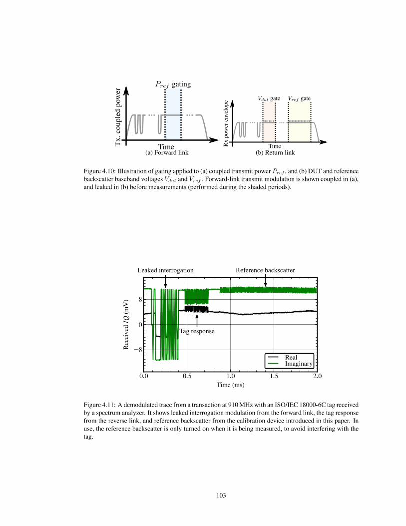
(a) Forward link (b) Return link
Figure 4.10: Illustration of gating applied to (a) coupled transmit power Pref , and (b) DUT and reference
backscatter baseband voltages Vdut and Vref . Forward-link transmit modulation is shown coupled in (a),
and leaked in (b) before measurements (performed during the shaded periods).
0.0 0.5 1.0 1.5 2.0Time (ms)
−8
0
8
Received
IQ(m
V)
RealImaginary
Leaked interrogation
Tag response
Reference backscatter
Figure 4.11: A demodulated trace from a transaction at 910 MHz with an ISO/IEC 18000-6C tag received
by a spectrum analyzer. It shows leaked interrogation modulation from the forward link, the tag response
from the reverse link, and reference backscatter from the calibration device introduced in this paper. In
use, the reference backscatter is only turned on when it is being measured, to avoid interfering with the
tag.
103

response to a query command.
Carrier phase noise at baseband was measured as large as 1.5 per symbol at 160 kHz, and as large
as 13 per 240 µs signal trace. Baseband drift is negligible between neighboring symbols noticable on
the scale of the full trace width.
Algorithmic determination of discrete signal state levels in pulsed or digital signals is known as
clustering. The usual approach is identify histogram peaks in VI and VQ [114], which has the advantage
of readily estimable uncertainty [115]. Unfortunately, the signal phase noise over the course of a frame
can be larger than the I and Q components and was often larger than the backscattered signal, making
the straightforward histogram analysis inapplicable.
The alternative clustering algorithm in the backscatter testbed is a one-dimensional application of the
Canny edge detection filter [116]. First, a discrete Gaussian filter is applied to the digitally sampled V
to remove noise without distorting pulse edges. The signal is approximately a sequence of rectangular
pulses between two signal levels, so its derivative should give “spikes” close to a discrete (Kronecker)
delta function at each transition. Thus, local amplitude maxima of the numerical derivative of the result
are reported as pulse transitions. The center 80% of the span between the time-value of each pulse
transition is recorded as a pulse state. Peaks greater than the signal standard deviation are recorded as
digital switches. The mean difference between neighboring pulses is recorded as the change in real and
imaginary components, ∆VI and ∆VQ.
Uncalibrated state changes in DUT and reference modulation are recorded as |∆Vdut| and |∆Vref | as
∆VI + j∆VQ. The corresponding DUT and reference power levels are Pbs,dut = |∆Vdut|2/(4Z0) and
Pbs,ref = |∆Vref |2/(4Z0) by equation (2.25). The calibrated DUT backscatter power, Pbs, is computed
with equation (4.14) by the procedure in Section 4.1.3.
Figure 4.12 shows a power sweep of the uncalibrated power measurements Pbs,ref and Pbs,dut, and
the calibrated Pbs. The reference power Pbs,ref is generated through the reference backscatter device
of Fig. 4.5. The very nonlinear power from the DUT tag, Pbs,dut, shows the expected sharp turn-on
threshold behavior as transmit power increases; below turn-on, the measured backscatter is equal to this
measurement’s noise floor below −90 dBm. Reference modulation power is very linear with transmit
104
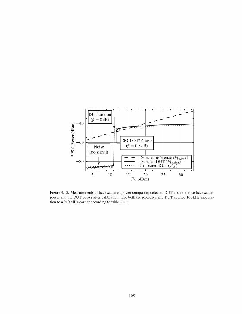
BPS
K P
ower
(dB
m)
Figure 4.12: Measurements of backscattered power comparing detected DUT and reference backscatter
power and the DUT power after calibration. The both the reference and DUT applied 160 kHz modula-
tion to a 910 MHz carrier according to table 4.4.1.
105

Network analyzer calibration ±0.25 dB
Power measurements ±0.25 dB
IQ level measurements ±0.05 dB
Noise and nonlinearity ±0.1 dB
Expanded uncertainty ±0.4 dB
Table 4.3: Estimated Backscattered Power Measurement Uncertainty Estimate (−60 dBm < Pbs <−20 dBm, 10 dBm < Pbs < 30 dBm, k = 2)
power, so the calibration factor K is approximately constant with input power in this sweep. Calibrated
DUT power, Pbs, is therefore offset from Pbs,dut by a constant.
4.4.2 Combined Uncertainty
To gauge the effectiveness of the reference backscatter calibration, an uncertainty estimate for calibrated
backscattered power measured with the testbed is presented in Table 4.4.2.
Reported values follow the methods for evaluating uncertainty discussed in 1.4, with each source
listed here in concise form. Each uncertainty term is the fractional uncertainty and combined according
to the law of propagation of uncertainty expressed in (1.23).
Testbed linearity is estimated from measurements of the reference backscatter as a function of power,
shown in Fig. 4.13. This measurement was performed with a bistatic receiver setup. Results between the
two traces agreed within ±0.1 dB, which is then the estimate for linearity and noise uncertainty.
Uncertainty in the IQ measurement processing, caused by ringing or level clustering errors, quoted
at ±0.05 dB, is based on monte carlo simulation of digital signals switched at 640 kHz, bandlimited to
12 MHz, sampled at 10 MHz, and with SNR limited to the Pbs,dut = −60 dBm lower specification limit.
Manufacturers provide detailed guidelines for estimating the uncertainty of power measurements.
The two are necessary for each Pbs calibration are conventional uses of power meters and sensors. The
±0.25 dB error estimate results comes by adding the correlated errors arithmetically, plus the RMS sum
of the uncorrelated error sources.
Uncertainty of a vector difference between two measured reflection coefficients to determine ∆ρ1 or
∆ρL is an interesting and nonstandard problem not addressed by in published literature or manufacturer
guidelines. Two approaches to estimating this uncertainty, 1) Monte carlo simulation and 2) estimating
106

5 10 15 20 25 30
−0.1
0
0.1
Transmit into ant 1
Transmit into ant 2
Figure 4.13: Reference backscatter linearity errors measured by sweeping transmit power and measuring
the reference backscattered power. The backscatter reference load-modulated 910 MHz carrier reflec-
tions at 160 kHz with the circuit described in Fig. 4.1. Deviation from linearity below 32 dBm input
power was less than 0.1 dB.
107

systemic errors that cancel in the two reflection coefficients, suggests uncertainty of about 0.25 dB. Inter-
estingly, for a wide range of different reflection coefficients, the uncertainty of a measured |∆ρ| is about
the same as that of a transmission coefficient, with a factor of√2 extra noise.
Other sources of error are small enough to be omitted from Table 4.4.2. After power calibration
against the reference backscatter, the relative error betweeen signal analyzer power measurements is
below 0.08 dB and contribute negligibly to combined uncertainty. Empirical tests also found less than
0.1 dB error in reorienting the location of objects in the test zone.
4.5 Summary
The devices and test methods proposed here generate reference signals suitable for transceiver or transpon-
der performance tests. For transponders, reference backscatter may be generated 1) through fixed-loss
coaxial networks and 2) over-the-air through antennas. For reader testing, another coaxial calibration
device can reflect adjustable modulation power into monostatic reader ports. Testbeds designed with
these calibration techniques are overspecified compared to realistic commercial test requirements.
Material in this chapter originated in the following peer-reviewed publications by the author:
D.G. Kuester, D.R. Novotny, J.R. Guerrieri, Z. Popovic, “Simple Test and Modeling of RFID
Tag Backscatter,” IEEE Trans. on Microwave Theory and Techn., vol. 60, no. 7, July 2012, pp.
2248-2258.
D.G. Kuester, D.R. Novotny, J.R. Guerrieri, R.H. Direen, Z. Popovic, “Reference Modulation for
Calibrated Measurements of Tag Backscatter,” Proc. 2011 IEEE Intl. Conf. on RFID, 12-14 Apr
2011.
D.G. Kuester, D.R. Novotny, J.R. Guerrieri, “Simple Test and Modeling of RFID Tag Backscatter,”
IEEE Trans. on Microwave Theory and Techn., vol. 60, no. 7, July 2012, pp. 2248-2258.
108

Chapter 5
Measurement of Passive Backscatter
Performance
Have no fear of perfection — you’ll never reach it.
Salvador Dalí (1904-1989)
5.1 Introduction
Chapter 3 identified two characterizations of tag backscatter performance: the BPSK radar cross Section
σ∆, which is essentially the existing metric, and the alternative figure of merit B at the core of this
thesis. Performance and conformance test standards ISO/IEC 18046-3 and ISO/IEC ISO18047-6 already
suggest some test methods for bistatic σ∆ [38, 41]. Even though these standards are targeted at RFID,
current tag datasheets do not give backscatter test data. It is clear the industry is not convinced that the
these data are useful enough to justify the cost of testing.
What are the benefits of backscatter test data? Accurate σ∆, coupled with reader sensitivity and
antenna performance data, gives an idea of the maximum detectable range of an RFID tag. Accurate B
gives an idea of the worst-case backscatter power received by the reader and thus, with reader sensitivity
performance data, give a lower bound for the SNR or SIR and thus communication error rate.
109

The analog identifier tag characteristic of [112, 113] is substantially similar to the special case B|p=1.
These seminal papers were published during peer review of the author’s metrology-focused [71]. The
goal in these references is tag “self-sensing:” sensing changes to the tag surroundings via changes to
B|p=1. Changes to B|p=1 were detected by measuring threshold transmit power from a commercial
reader, Ptx0, and corresponding backscattered power, Pbs|p=1. The fact that a reader is not a calibrated
measurement instrument is not a problem for these relative measurements: reader linearity and relative
error were found by calibrating against initial results, so absolute accuracy of B|p=1 was not important.
A technical challenge that has not yet been resolved in this approach to sensing is controlling thermal
stability of the uncalibrated measurements of B|p=1.
In contrast, measurements of B in this thesis are meant for link modeling and determining min(Pbs).
The power levels are only meaningful if they can be compared directly, which requires measurements
traceable to fundamental power and S-parameter standards. These two physical quantities, when mea-
sured with qualified power sensors or network analyzers, are traceable against standards from national
metrology institutes like NIST. The previous chapter gave test methods for traceable power measure-
ments of Pbs and Ptx.
This chapter investigates the use of calibrated power measurements to determine B and the BPSK
RCS, σ∆. With an estimate of the uncertainty of these measurements, a coaxially connectorized RFID
tag is constructed that validates both the model and theory of B. These results confirm that the theory
predicts B (and thus min(Pbs)) to within the predicted ±0.43 dB tag measurement testbed uncertainty
in an anechoic environment.
5.2 Uncertainty: How Good is “Good Enough?”
The central goal of RF measurement in this thesis is to support analysis of signals power to estimate
communication error rates as a reliability metric. Lower measurement uncertainty, and the corresponding
expectation of improved measurement accuracy, can often be realized at the expense of added time,
effort, and cost. Comparison of the measurement costs against the benefits of lower uncertainty requires
some understanding of test uncertainty propagates to uncertainty in the link analysis.
110

Estimates of received backscattered power Pbs depend on measured tag performance via σ∆ or B,
so uncertainty in either of these affects the uncertainty of the predicted Pbs. If the uncertainty of Pbs
is increased, then minimizing communication errors requires tighter specifications in the form of im-
proving reader sensitivity, or possibly derating system performance in terms of tag operating range or
communication error rate.
5.2.1 Measurements Uncertainty of σ∆ vs. Pbs
We can begin with the general Pbs ∝ σ∆/L2, since σ∆ ∝ ηmod. As before, L is available power loss
between the transmitter and load modulation, and ηmod is the proportion of incident power re-reflected
by the load modulator as BPSK modulation.
Consider any two independent random variables X and Y . The variance of their product obeys the
identity [117]
Var(XY ) = [E(X)]2Var(Y ) + [E(Y )]2Var(X) + Var(X)Var(Y ), (5.1)
and, because they are independent,
E(XY ) = E(X)E(Y ). (5.2)
Thus
Var(XY )
[E(XY )]2=
Var(X)
[E(X)]2+
Var(Y )
[E(Y )]2+
Var(X)
[E(X)]2Var(Y )
[E(Y )]2. (5.3)
The square root of each side of this equation relates the fractional variances of the product XY to the
fractional uncertainties of X and Y .
Similarly, because σ∆ and 1/L2 are independent and Pbs is proportional to their product, their rela-
tive variances are:
Fractional variance of Pbs =
√
Var(Pbs)
[E(XY )]2
=
√
Var(σ∆) + Var(1/L2) + Var(σ∆)Var(1/L2).
(5.4)
Here, Var(·) is fractional variance (variance normalized to [E(·)]2). The distribution of our stochastic Pbs
is therefore always more spread out than either the sum or the product of its parts.
111

The relative contribution of σ∆ uncertainty onto the variance of Pbs is thus
Var(Pbs)
Var(1/L2)=
√
1 +Var(σ∆)
Var(1/L2)+ Var(σ∆). (5.5)
In the limit of strong fading, the variance in 1/L2 is large, and the center term in the radix becomes
negligible,√
Var(Pbs)
Var(1/L2)≈√
1 + Var(σ∆). (5.6)
Figure 5.1 illustrates implications of equations (5.4) and (5.6). Discussion so far has been general
for any distribution of Pbs and σ∆. To connect variance with uncertainty discussed in Section ??, the
illustration assumes normally-distributed combined error in σ∆ with coverage factor 2, and thus the
value√
Var(σ∆)/2. The representative range of fractional uncertainties is broad: 0.5 dB is better than
any claimed in the literature, 2 dB is reasonable for the anechoic measurements of [45], and 6 dB is
observed in a storage room in Section 5.4.
The curves of Fig. 5.1a show that when the standard deviation of backscattered power in the realistic
environment is greater than the σ∆ uncertainty, the contribution of uncertainty in σ∆ to uncertainty in Pbs
becomes approximately constant. The additional uncertainty in Pbs in this limit is plotted in Fig. 5.1b.
In this limit, the uncertainty added to our stochastic Pbs is always less than the uncertainty of σ∆.
The definition of what is a “good enough” uncertainty result in measured σ∆ therefore requires a
choice about an acceptable increase in uncertainty in Pbs. Two good rules of thumb come from Fig. 5.1b
in strong multipath environments: first, measurement uncertainty below 4 dB affects the uncertainty of
Pbs by less than 1 dB; second, measurement uncertainty below 2 dB affects the uncertainty of Pbs by less
than 0.2 dB. The latter is a reasonable expectation with existing test methods outlined in the next Section
[45, 46], making the contribution of σ∆ to predictions of realistic monostatic Pbs quite small.
5.2.2 Measurements Uncertainty of B vs. min(Pbs)
Analysis of uncertainty of min(Pbs) with B is much simpler, because the only concerns are:
(1) measurement uncertainty in B (addressed in the next chapter with design of the measurement
testbed); and
112
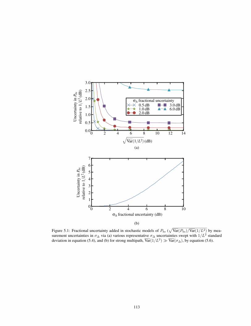
(a)
(b)
Figure 5.1: Fractional uncertainty added in stochastic models of Pbs (√
Var(Pbs)/Var(1/L2) by mea-
surement uncertainties in σ∆ via (a) various representative σ∆ uncertainties swept with 1/L2 standard
deviation in equation (5.4), and (b) for strong multipath, Var(1/L2) ≫ Var(σ∆), by equation (5.6).
113

(2) uncertainty in Ptx, which is small and negligible.
The uncertainty of min(Pbs) from test data is therefore approximately the same as the uncertainty of
B. If B is measured accurately and detuning of B can be controlled, then an estimate of the min(Pbs)
bound is also very accurate.
5.3 Prior Art: Anechoic RCS Measurements in ISO 18047-6
The only prior work the author has identified about digitally modulated backscatter communication
metrology is applied to UHF RFID, and is encapsulated inside ISO 18047-6 [41].
5.3.1 Procedure: ISO 18047-6 (2006 version)
The 2006 version of UHF RFID test standard ISO 18047-6 [41] (now obsolete) was the state of the art
when this work began. It contains test recommendations for σ∆ that calibrate receive tag signals against
carrier scattering measurements off of a thin λ/2 rod. This rod is the CW “calibration target.” This test
approach is similar to many RCS measurements for which the DUT is a passive structure that reflects
only CW.
Tests that emulate this behavior are shown in Fig. 5.2. The shorted dipole mimics the thin rod used for
tests. Two discrete states are presented to the measurement receiver by manually inserting and removing
the entire reflecting structure. This approach also allows study of transmission behavior to the dipole. The
standard prescribes a bistatic testbed antenna configuration, though monostatic σ∆ is measureable with
the same kind of test. The method is simple, though it is revised here slightly to correct the problematic
use of power envelope detection described in Section ??.
Chapter 2 shows that detection of digitally modulated backscatter requires an IQ detector. The cor-
responding phase component is included by network analyzer measurement of the change in complex
S-parameters looking into the “reader” antenna; |∆ρ1|/42 or |∆τ21/4|2 approximates Pbs/Ptx given the
well-matched network analyzer. Since the change in ρ1 is realized by adding and removing the entire
scattering structure, we are thus modulating both the antenna mode reflections (by adding and insert-
114

ing the load) and the structure of the antenna. In the free field, we therefore expect that Pbs/Ptx is
proportional to the total CW RCS, σ (not the load-modulated BPSK RCS σ∆ of (3.22) via the radar
equation.
First, a network analyzer measures |∆τ(ref)21 |2 (or |∆ρ
(ref)1 |2 in monostatic setups), from measured
states corresponding to transmission between the bistatic testbed antennas 1) loaded by the calibration
target, then 2) unloaded. It is calibrated with an electronic calibration unit to a reference plane defined
at the patch antenna’s coaxial input port. This is the calibration reference target with some known cross-
Section σ. For the thin λ/2 rod, various results give σ within the range 0.6λ2 to 0.9λ2 [Green1962, 118,
119]; the 2006 version of ISO 18047-6 prescribes a single value to use as σ. A correction factor, “K,” is
taken to encompass the unknown terms of the radar equation:
|∆τ(ref)21 |2 = Kσ, (5.7)
where
K =G2
tx(θtx, φtx)λ2
(4π)3r4|u3 · utx|2. (5.8)
Note that there is no ηrx/ηtx factor in K, because it cancels with the network analyzer defined as
ρI1 = 0, and further the transmit and receive antennas are implicitly assumed to be well matched to
an unspecified extent.
The test zone is now empty, because the reference target was removed in the measurement of |∆τ21|2.
To measure the DUT, we place it centered exactly where the reference target was located, replacing the
network analyzer with an IQ receiver (such as a signal analyzer). Measuring the BPSK power received
from the tag, Pbs, and assuming K is unchanged from (5.8), we get the BPSK radar cross Section of the
DUT:
σ∆ = σPbs
Ptx|∆τ
(ref)21 |2
= σ(ref)(θ3, φ3)1
K
(5.9)
The main errors here are not obvious from these simple equations. First, the calibration target is
detected with a network analyzer (calibrated to an unspecified reference plane), but DUT backscatter is
received by a completely different instrument like an oscilloscope or signal analyzer. Before the writing
115

Scatterer Measured |∆τ21|2Thin λ/2-long rod RCS target -40 dB
Engineer in the chamber door -49 dB
Pen left in chamber (r = 1m) -45 dB
Small RFID tag left in chamber (r = 1m) -49 dB
Accidentally rotate reference antenna ±15 -41 dB
Table 5.1: Measured |∆τ21|2 for some unintended events in the test zone
of this thesis, there was no prescribed method for calibrating detection of Pbs. Second, K is only constant
in each measurement if the entire test setup is undisturbed each of the 3 times the operator enters and
exits the chamber. Any displacement of walkway absorber, antenna positions or orientations, or receiver
cables changes K and adds error to the measurement of σ∆. Some examples of measured changes in
|∆τ21|2 seen in the NIST RFID test chamber are listed in Table 5.1, shown for comparison with the
measured value of the calibration target.
5.3.2 Procedure: ISO 18047-6 (2011 version)
The 2011 update to ISO18047-6 adopts changes from [44] in measurements of σ∆. It is almost opposite
of the 2006 version: instead of calibration against a known scattering target, each term in the radar
equation is computed or measured separately.
In terms of (3.18):
σ∆(θ3, φ3) =Pbs
Ptx
ηtxηrx
[
Gtx(θtx, φtx)Grx(θrx, φrx)λ2
(4π)3r2txr2rx
|uant,tx · utx|2]−1
. (5.10)
It is reasonable to assume here that the testbed can be built with a well-matched receiver and transmitter
and antennas, so we neglect mismatch. This leaves Pbs, Ptx, G, reader antenna gains, and the polarization
terms to be measured.
5.4 Multiple Reflection Errors in RCS Calibrations
In moving toward environment-independent tests from the standardized RCS test methods described in
the previous Section, a logical next step is to consider the effects of the environment on these tests.
Careful control over the test environment can minimize measurement errors from antenna detuning and
116

ambient electromagnetic interference, and help to maintain adequate measurement dynamic range. In
contrast, errors from multiple reflections in an “anechoic” test environment are challenging to quantify
and costly to mitigate.
Reflections in the environment contribute differently to the uncertainty of the DUT σ∆ measurement,
depending on whether the 2006 or 2011 type of measurement is performed. In the “direct” σ∆ test of
Section 5.3.2, any relative error in propagation loss compared to 1/r4 adds the same relative error to the
measured σ∆. A subtler problem posed by multiple reflections in calibrations against CW RCS targets
(as in Section 5.3.1) is that structural-mode scattering from the calibration reference target perturbs
standing waves in the test area, while there is no structural-mode modulation in signals from the tag
DUT. Otherwise, as long as the gain patterns of the DUT are similar to a λ/2 dipole, we could naïvely
expect that multiple reflections would have the same effects on both the calibration reference target and
the DUT.
This Section considers these multiple reflection effects on σ∆ tests by comparing measurements taken
in a semi-anechoic environment and repeated in a more reflective storage room. The measurements
are illustrated by Fig. 5.2. First, 1/|E31|4 ≈ L2 between the patch and dipole is measured as the
antenna-mode backscatter loss, with S-parameters calibrated as shown in Fig. 5.2a. This emulates losses
experienced by a load-modulated passive tag. The reflection coefficient at one of the “reader” patch
antennas is measured in each of the two states of the calibration target simulated in Fig. 5.2b: the test
environment (1) with, then (2) without the shorted dipole and matched feed. The magnitude of the
difference between the two values is reported as |∆ρ1|2, proportional to backscatter power introduced
by the target RCS and its interaction with the environment. The noise floor of |∆ρ1|2 measurements was
lower than -75 dB across 700-1100 MHz.
The patch and dipole antennas are oriented to boresight with a laser square and co-polarized with a
level in each E31 and |∆ρ1| measurement. The range r between the two antennas, shown dotted in Fig.
5.2, is measured by laser range finder in each experiment.
117

(a)
Port 3Port 1 r
Propagation effects(S-parameter network E)
(b)
(1)
Port 1Short
Port 3
(2)Port 1
50 Ohm
(dipoleremoved)
r
Port 350 OhmPropagation effects(S-parameter network E')
Propagation effects(S-parameter network E)
Figure 5.2: Scattering measurement setup. In the forward link configuration (a), a full two-port measure-
ment was performed with the network analyzer, calibrated to the S-parameter reference planes shown;
measurements of |E31|2 are taken to describe link losses. In the reverse link measurement (b), measure-
ments of the 1-port reflection coefficients ρ(1)1 and ρ
(2)1 give difference |∆ρ1|2. This emulates ISO/IEC
18047-6 tests and gives transmission loss via L ≈ 1/|E31|2.
118

|E31|4 |∆ρ1|2 Apparent phase-
Std. Dev. Worst Std. Dev. Worst center offset
CP patch 0.10 dB 0.48 dB 0.22 dB 1.1 dB 0.008 - 0.049 m
LP patch 0.14 dB 0.46 dB 0.45 dB 1.5 dB 0.042 - 0.059 m
Table 5.2: Regression information from Fig. 5.4 within 895-935MHz
5.4.1 Measurements in an Anechoic Environment
The author constructed a cubic semi-anechoic chamber with 2.4 m walls on each side with an open
top leading to another anechoic surface at the lab ceiling 7.6 m above. It is pictured in Fig. 5.3. The
centerpiece of this aesthetically optimal carpentry exercise is a foam table, which supports lightweight
calibration or DUT targets. Absorber cones are 30 cm long, except opposite the interrogation antennas,
which are 60 cm long to maximize absorption in the main beam of the testbed antennas.
In front of one wall is a mount for one or two interrogation antennas to support monostatic or bistatic
operation. Two commercially-available patch antennas with peak gain 8.5 dBi and return loss greater
than 25 dB 902-928 MHz are on hand: one was linear polarized (LP), and the other circular polarized
(CP).
A straightforward approach to estimating multiple reflection errors in the test zone is to measure
the square of transmission, |E31|4, and backscatter, |∆ρ1|2/4, swept with interrogator-to-target antenna
separation r. Both should follow 1/r4 closely; regression error relative to this trend will suggest the
uncertainty due to reflections and misalignments in the test zone. These results give an idea for typical
errors in testing DUTs that have broad gain patterns.
Semi-anechoic room measurements are shown in Fig. 5.4 with a regression −10 log10(r4). Statistics
are computed in linear units before conversion to dB. The residuals listed in Table 5.2 give an idea for
the multiple reflection errors in the test zone in this anechoic environment. The scattering measurements
in the anechoic environment do decay as 1/r4, with a conservative rough uncertainty of around ±1 dB
to ±2 dB. These are limited by a combination of the [im]precision of the hand-measured antenna posi-
tioning and orientation and standing waves caused by reflections in the test zone. Because 1/L2 is much
smaller than Pbs/Ptx, the relative error between antenna-mode scattering and the CW RCS calibration
target here also gives uncertainty of around ±1 dB to ±2 dB. If a scattering target with modulated loads
119

Figure 5.3: The measurement setup in the semi-anechoic chamber. The LP reader antenna is shown
attached to the mounting structure on the left, and the target dipole is on the right.
120
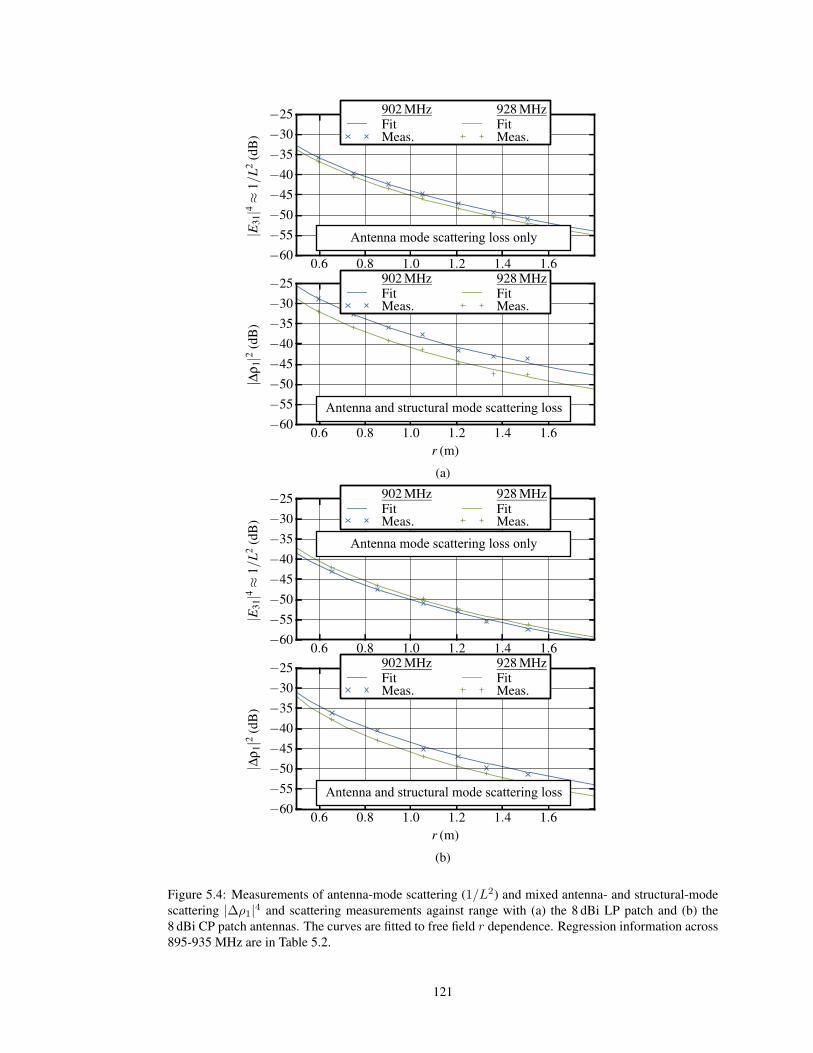
Antenna and structural mode scattering loss
Antenna mode scattering loss only
(a)
Antenna and structural mode scattering loss
Antenna mode scattering loss only
(b)
Figure 5.4: Measurements of antenna-mode scattering (1/L2) and mixed antenna- and structural-mode
scattering |∆ρ1|4 and scattering measurements against range with (a) the 8 dBi LP patch and (b) the
8 dBi CP patch antennas. The curves are fitted to free field r dependence. Regression information across
895-935 MHz are in Table 5.2.
121

ISO 18047-6 (2006): ISO 18047-6 (2011):
Calibration against No calibration
CW RCS standard (only radar equation)
Semi-anechoic chamber 1.5 dB 0.5 dB
Storage room 6 dB 6 dB
Table 5.3: Estimates of worst-case standing wave error relative to ideal free space
were available as a calibration reference, positioning and reflection errors would be less than ±1 dB,
following |E31|4, even with the transmission measurement cable.
Assuming these results are representative of the dominant error in the measurements, both of these
test procedures fit the goal of less than 2 dB uncertainty that we determined in Section 5.2.
5.4.2 Storage Room Results
ISO 18047-6 measurements in a large non-anechoic room with the penalty of increased measurement
uncertainty are one approach to reducing σ∆ test costs. These more reflective environments are already
often used for the simple “read range” tests reported by many manufacturers.
Measuring structural mode components in a more reflective environment via |∆ρ1|2 and comparing
against the anechoic room results can give some insight here. The storage room pictured in Fig. 5.5
presents many potential sources of scattering to the reader antenna. The author performed measurements
here under the same procedure as in the semi-anechoic environment. Line-of-sight was maintained
between the antennas in all tests.
Results are plotted in Figs. 5.6 and 5.7 swept with range, with the reader antenna position kept
fixed. To make the effects of multiple reflection clear, results from the storage room environment are
normalized to semi-anechoic chamber data. Transmission and backscatter losses vary by up to about
10 dB compared to the anechoic environment. Standing waves between the target and the floor also give
about 1 dB of ripple in the CP patch data.
These data result in the σ∆ test uncertainty estimates in the two environments compared in Ta-
ble 5.4.2. Both are assumed dominated by propagation and misalignment errors measured here. The un-
certainty in the storage room is about 6 dB with both the CW RCS calibration method (from |∆ρ1|2/4/L2)
and by direct use of the radar equation (by directly examining 1/L2).
122

Figure 5.5: A reverberant environment. The ceiling, walls, and floor are steel-reinforced concrete. There
is a large outdoor-facing window above the frame of the photograph, a large workbench and wall in the
rear, shelving containing with test equipment on the right and left.
123

r = 0.6 m
r = 1.0 m
r = 1.5 m
r = 2.0 m
Figure 5.6: LP transciever antenna backscatter loss, measured in the environment pictured in Fig. 5.5.
Normalization is against the anechoic results of Fig. 5.4, at each separation distance r. “Antenna and
structural mode” scattering is |∆ρ1|2 found by adding and removing the shorted dipole RCS standard;
“antenna-mode only” scattering is |E31|4 ≈ 1/L2.
124

r = 0.6 m
r = 1.0 m
r = 1.5 m
r = 2.0 m
Figure 5.7: CP transciever antenna backscatter loss, measured in the environment pictured in Fig. 5.5.
Normalization is against the anechoic results of Fig. 5.4, at each separation distance r. “Antenna and
structural mode” scattering is |∆ρ1|2 found by adding and removing the shorted dipole RCS standard;
“antenna-mode only” scattering is |E31|4 ≈ 1/L2.
125

Figure 5.1b suggests that even under the best case of very strong fading, we expect to add about
3 dB to stochastic estimates of Pbs. This may be significant relative to a backscatter link margin, and
represents uncertainty in coverage range of about 40%.
Thus, the radar cross Section test methods discussed here yield “good enough” uncertainty in reflec-
tive indoor environments typical of engineering labs. Environmental effects with the new test method
proposed in [120] have not yet been investigated; its use of a load-modulated calibration standard may
reduce uncertainty in σ∆ calibrations in non-anechoic environments.
5.5 Measurement of B
Calibrated measurements of Ptx and Pbs give B in decibels defined here as
B (dBm)2 = Ptx0 (dBm) + Pbsηtxηrx (dBm)
= 10 log10 [Ptx0 (mW) × Pbsηtxηrx (mW)] .
(5.11)
The nonstandard decibel unit here, (dBm)2, is as defined in (3.31).
The goal of the measurement described in this Section is the ideal B in an anechoic environment.
Thus, the effect of reflectors on the tag antenna impedance (detuning) is considered a measurement error.
In measurements performed in a realistic environment, tag detuning could be part of the measurement
instead of the error.
Since measurement and uncertainty of Pbs is discussed in Section ?? and measurement of the carrier
transmit power is broadly understood, we primarily consider combined uncertainty effects on B.
5.5.1 Nonlinearity Sweeps
The calibration procedures given for tag backscatter measurements in Chapter 4 all assume that detection
and reference backscatter are all ideally linear with respect to power. Thus, any nonlinearity in the
measurement testbed is a source of error that needs to be considered in the uncertainty analysis process.
The signal analyzer specifies the error at a few hundredths of a decibel (about 1% linear), and the power
sensor specifies 0.1 dB (about 2.5% error). The solid state switch for reference backscatter has negligible
nonlinearity error from compression below 29 dBm.
126
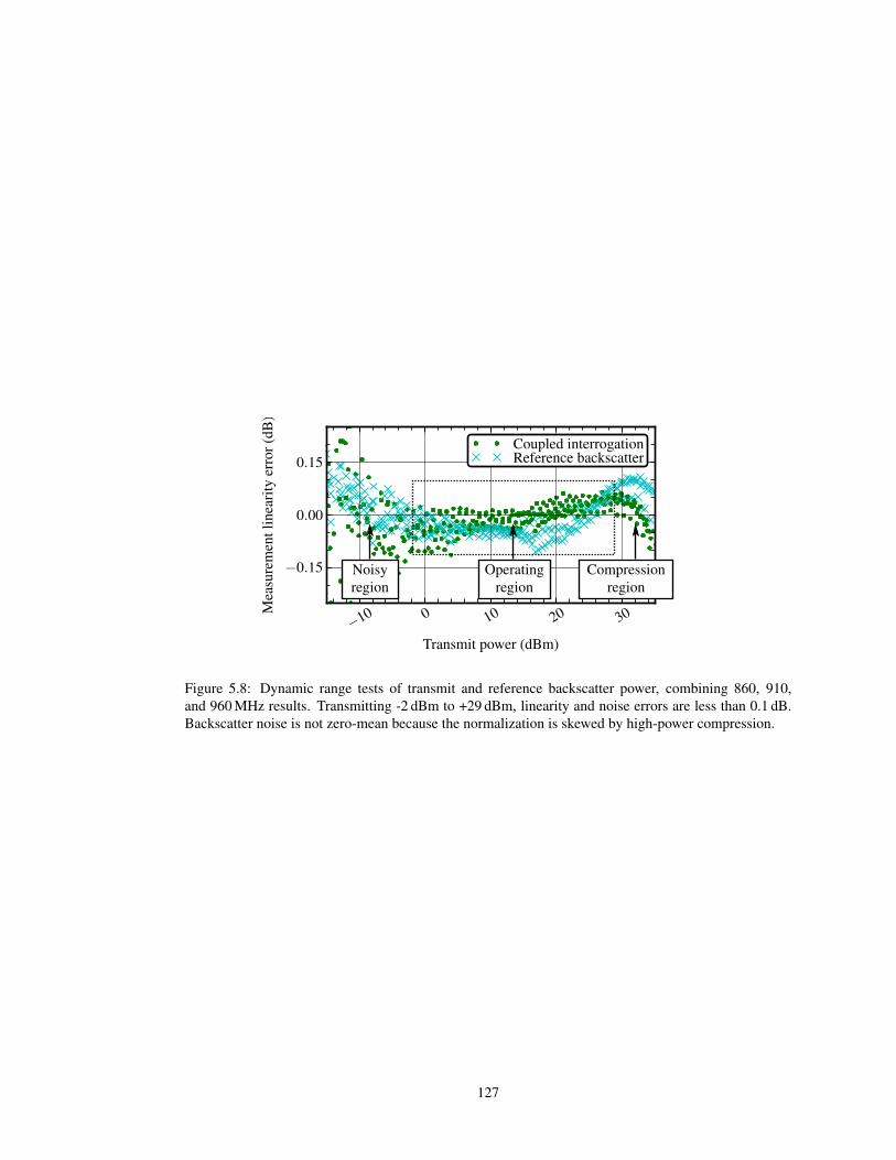
Figure 5.8: Dynamic range tests of transmit and reference backscatter power, combining 860, 910,
and 960 MHz results. Transmitting -2 dBm to +29 dBm, linearity and noise errors are less than 0.1 dB.
Backscatter noise is not zero-mean because the normalization is skewed by high-power compression.
127

Coupled interrogation power and reference backscatter power are swept with transmit power in Fig.
5.8 to validate that the combined system meets specification. Results are re-normalized against transmit
power. The result is a plot combining thermal noise and nonlinearity errors of each measurement. Within
the specified -2 dBm to 29 dBm transmit power range, these errors are within ±0.1 dB. The standard
deviation of either the power sensor measurement and the backscatter power measurement is 0.04 dB if
transmit power is within the specified -2 dBm to +29 dBm operating range. Several power measurements
in the calibration process cancel, and the uncertainty in B from noise and nonlinearity is thus about the
same as the RMS sum of the backscatter and power measurement uncertainties at 0.05 dB.
5.5.2 Tag Turn-on Power Level Errors
One source of error is truncation (round-off) in controlling the testbed transmit power level. The res-
olution is 0.1 dB. The error in Ptx0 and therefore reference backscatter power is therefore uniformly
distributed between 0 and +0.1 dB, with a bias of +0.05 dB (errors in dB behave approximately linearly
here because they are so small). In post-processing, Ptx0 and Pbs,ref are therefore increased by +0.05 dB
to remove the bias, so the maximum error is ±0.05 dB and the standard deviation is ±0.015 dBm.
5.5.3 Tag Detuning Sweeps
Measurements of a commercial tag are swept with distance from the testbed antenna mount in Fig. 5.9.
The test environment is the anechoic chamber. Measurements are performed at about λ/4 increments
across 2λ at 900 MHz, ensuring better than Nyquist sampling and a transmit power swept from 0 dBm
to 25 dBm. The result is a plot of standard deviation (caused by combined noise, nonlinearity, and tag
antenna detuning errors) and mean at each frequency.
Standard deviation at each point is as large as about 0.1 dB. Variance at each frequency is a combina-
tion of unknown thermal noise, tag detuning by non-ideal reflectors in the anechoic environment, nonlin-
earity errors, and uniformly-distributed noise in truncating Ptx to 0.1 dB (standard deviation 0.015 dB).
The errors included in 5.5.1 suggests that thermal noise nonlinearity errors have combined standard de-
viation of 0.05 dB. These error sources and (1.23) give the remaining error source, tag antenna detuning,
128

Table 5.4: Testbed specifications, 860-960 MHz
Antennas 8 dBi LP patches
Antenna isolation
Empty chamber load > 45 dB
Detuning plate 1 m away > 30 dB
Ptx0 resolution 0.1 dB
Transmit power −2 to +29 dBm
Mismatch errors < 0.06 dB
IQ noise -135 dBm/Hz
Tag backscatter sensitivity -67 dBm
(50% detection rate)
as having standard deviation of 0.08 dB.
Since the standard deviation caused by tag detuning is about 0.08 dB, the final expanded uncertainty
estimate for tag antenna detuning errors is 0.16 dB. A more accurate estimate might might come from
assuming a U-shaped distribution of the detuning error instead of a normal distribution, which would be
appropriate because it is caused primarily by mismatch [65][66].
Theory in Chapter 3 predicted that B should be more stable in reflective environments than σ∆.
Comparing tag antenna detuning in measurements of B, with 0.07 dB standard deviation, against the
0.45 dB standard deviation in σ∆ measurements (from the results in 5.4) validates this premise. Each
measurement uses the same linearly-polarized (LP) patch antenna in the testbed in the same environment,
yet the errors from test zone reflections are about six times smaller for B as σ∆.
5.5.4 Combined Uncertainty
Table 5.4 lists performance parameters of the testbed illustrated in Fig. 4.9. Because Pbs is proportional
to B, uncertainty in a tag’s figure of merit contributes the same uncertainty to backscattered power
estimates in link analysis.
The range of measurable B in the testbed depends largely on DUT placement in the test zone. Placing
the tag co-polarized and in the main beam of the testbed antennas helps ensure turn-on and that backscat-
ter is far above the −67 dBm testbed sensitivity. If Ptx0 < −2 dBm, the tag must be moved farther from
the testbed antennas to maintain specified measurement linearity. Tags tested by the author fall within
−35 (dBm)2 < B < −15 (dBm)2, all measurable near the main beam of the 8 dBi patch antennas at 1 m.
129

Figure 5.9: Mean and standard deviation of B measured at 8 positions in the test zone, from 60 cm to
120 cm (approx. 2λ to 4λ) away from testbed antennas in 7.5 cm (approx. λ/4) steps. At worst, standard
deviation is below 0.1 dB, which we believe is dominated by noise.
Future tags with smaller PL0 will tend toward smaller B.
These results contribute to the estimate of combined uncertainty of B listed in Table 5.5.4. The
remaining uncertainty estimates are based on uncertainty analysis documentation provided by the man-
ufacturer of the power sensor and network analyzer, and with network analyzer verification impedance
standards. The final combined uncertainty of ±0.43 dB (±11%) is computed from their quadrature sum
according to (1.23).
5.6 Validation of B Theory and Measurements
A tag built from a connectorized antenna and chip is shown in Fig. 5.10. It enables separate antenna and
chip impedance measurements to validate the testbed accuracy and the theory regarding B without the
complexity of probe and bonding parasitics. A commercially available tag chip package, marketed as
compliant with [2], is soldered directly onto an SMA connector. Its input impedance is transformed to
near 50Ω within 860-960 MHz by single-stub matching. The antenna is a commercially available dipole
tuned to 910 MHz with an integrated 2:1 balun.
On-tag circuit parameter measurements for B are not typically practical, but are helpful here to
validate our model and testbed. Other work has addressed the problem of measuring the power harvesting
impedance state [121, 122] with a network analyzer at a calibrated power level. Our network analyzer
130

Error source Expanded Uncertainty Estimate
Reference modulation calibration ±0.25 dB
Power measurements ±0.25 dB
Multipath ±0.16 dB
Coupler calibration ±0.15 dB
Testbed nonlinearity and thermal noise ±0.1 dB
Combined expanded uncertainty of B ±0.43 dB (±10%)
Table 5.5: Expanded uncertainty estimates for reported B
Figure 5.10: Connectorized “validation tag,” stub-matched to 50Ω. Measurements are calibrated at the
dashed line. The 15 cm dipole has an integrated wideband 2:1 balun and |ρR| < −10 dB across 860-
960 MHz.
131

(a)
(b)
Figure 5.11: Measurement configuration for (a) ρR, which is calibrated against (b) ρL. Power at network
interfaces (dotted lines) are calibrated at Ptx0 by power sensor.
cannot excite or measure the time-varying reflective state ρR, so we constructed a custom reflectometer
like [87, 123] calibrated against the power harvesting state.
First, the turn-on power into the chip network is determined by adjusting the power out of the in-
terrogator in Fig. 5.11(a), and measuring power at the given interface with a peak power sensor as
described in Section ??. Measurements of ρL0 and ρL, are performed at a fixed p, fed with the 50Ω
network analyzer as a generator. The sensitivity of the chip network is then computed from a power
sensor measurement at the coupler output Pmeas with PL0 = Pmeas/(1 − |ρL0|2), assuming that the
coupler and reader are matched 50Ω sources. PL0 was within 0.2 dB of -13 dBm across the band.
With ρL0 known, reflections in each chip impedance state coupled into the spectrum analyzer can be
compared to determine ρR. If the coupler and instruments are well matched, and the coupler has infinite
directivity, the two reflection coefficients would be equal to the ratio of the complex IQ measurements
VR/VL at a given forward-wave voltage Vtx,
ρRρL
=VR/Vtx
VL/Vtx=
VR
VL. (5.12)
We also used the thorough directional coupler analysis in [124] to account for coupler directivity and
mismatch uncertainty at the chip interface:
ρR =d(VR/VL − 1) + (VR/VL)ρL
1− ρLρc(VR/VL − 1), (5.13)
132

(a) (b)
Figure 5.12: Measured efficiency of the tag pictured in Fig. 5.10, at turn-on and at p = 0.8 dB. Measured
data shown in the 50Ω smith chart in (a) were used to compute matching and modulation efficiencies ηL0
and ηmod in (b).
where d is the complex parameter determined from S-parameters such that the coupler directivity is
D = −20 log10 |d|, and ρc is the reflection coefficient of the coupler at the network interface with the
connectorized chip network. Measurements d and ρc calibrate the final ρR.
Computing ηmod(p = 0.8 dB) and ηL0 from equations (3.6) and (3.9) with the circuit measurements
gives the performance summarized in Fig. 5.12.
B predicted by (3.28) from these measurements are compared against testbed measurements in Fig.
5.13. Fig. 5.13(a) shows a frequency sweep with the validation tag on a polystyrene table (ǫr ≈ 1).
Fig. 5.13(b) compares predicted B of the validation tag at three frequencies detuned by a 70 cm ×
70 cm aluminum plate. Circuit efficiencies were recalculated with measurements of the antenna reflection
coefficient at each height. In all cases, the predicted B agree to within ±0.35 dB, which is within the
±0.5 dB testbed uncertainty.
5.7 Summary
This chapter has compared the accuracy of radar cross Section and backscatter figure of merit mea-
surements, and propagation to estimates of received backscatter power. The received power estimate is
always at least slightly greater than the uncertainty of the tag backscatter metric used to estimate it. Un-
133

21
19
23
25
27
(a)
(b)
Figure 5.13: Validation of (3.28) by measurements of B. The setup detailed in Section ?? gives “testbed”
B. “On-tag” B are from parameters in Fig. 5.12. Measurements in (a) an anechoic chamber normalize
(b) detuning by an aluminum plate. All curves agree within the 0.5 dB testbed uncertainty.
134

certainties for radar cross Section measurements contribute negligibly to uncertainties in received power,
as long as multipath is weak. In contrast, uncertainty of a minimum backscatter power bound estimate
is the same as the measurement uncertainty of B. Thus, estimates of minimum backscatter power with
measured B are always more accurate than estimates of backscattered power with σ∆.
D.G. Kuester, D.R. Novotny, J.R. Guerrieri, Z. Popovic, “Simple Test and Modeling of RFID
Tag Backscatter,” IEEE Trans. on Microwave Theory and Techn., vol. 60, no. 7, July 2012, pp.
2248-2258.
D.G. Kuester, D.R. Novotny, J.R. Guerrieri, “Simulated Link Relationship Measurements for
Load-modulated RFID,” Proc. 2010 Antenna Measurement Techniques Association Symp..
135

Chapter 6
Test and Analysis for Reliable Passive
UHF RFID Communication
You have my permission to play great.
Dr. William J. Stanley
6.1 Introduction
The previous chapters have proposed that B has strong advantages in simplifying theory and measure-
ment of backscatter from passive UHF RFID tags. These advantages are meaningless, however, unless
B can provide some useful insight into the behavior of a communication system. This chapter discusses
how B applies to the simplest and most common type of UHF RFID, monostatic passive systems in the
far field.
Even after 8 years of standardized operation, little guidance has been published on test or modeling
of return links, but reliable systems have still been deployed. Moving forward, however, as readers
and tags improve, system dynamics are moving reliability constraints away from the power harvesting
performance and toward the return link.
The important effect of backscatter power on users is its effect on overall communication reliability.
136

Tag inventory rates are more readily observable and measurable than signal levels, and have a more direct
impact on a system’s practical utility. Thus, we need to be able to both 1) predict backscatter power seen
by a reader, but also 2) translate backscatter power into information about inventory rates that are visible
to users.
Predicting signal power in each link requires data about the communication devices and the radio
environment. Devices can be measured and tested in a laboratory. Most systems are deployed indoors in
industrial or commercial environments. These rooms have arbitrarily sized and positioned objects that
act as radio wave scatterers and absorbers, causing signal attenuation (fading) that can prevent communi-
cation. Attenuation of transmit signal amplitude with strong scattering sources is modeled as a Rayleigh-
or Rice-distributed random variable that has large variance.
The traditional approach to estimating wireless communication errors and throughput rates requires
random fading channel loss estimates. Stochastic modeling of the backscatter return link is poorly un-
derstood. Indoor propagation of backscatter communication has only been studied in a few papers.
Theoretical study has been performed primarily to support backscatter communication at 5.8 GHz [125,
126] rather than the more common 900 MHz. Monostatic UHF backscatter channel data were measured
in [127], but strangely fit to a Rayleigh random variable (not Rayleigh squared) like a transmission link.
Empirical propagation data are scant and difficult to compare. Other fading measurements and simula-
tions do not separate the two links [34, 128–130], distorting the resulting fading. None of these have
yet studied the performance of return links given the condition that the power harvesting link works
correctly.
This chapter brings B into passive RFID system analysis to provide guidance on improving commu-
nication reliability through robust return links. The minimum backscatter power is shown to relate to a
minimum expected inventory speed, depending on reader performance. Measurements of performance
of 20 commercial RFID tags and 5 commercial RFID readers give an quantitative idea of realistic de-
vice performance. The minimum power predicted by B is then combined with device performance to
demonstrate prediction of minimum inventory rate in a low-interference environment. The final result is
a system design procedure to guarantee reliable inventory speed.
137

6.2 Reliability in an AWGN-limited Channel
A mathematically rigorous definition of reliability is beyond the scope of this thesis, but some discussion
of general concepts in the context passive backscatter communication here will inform reader and system
test strategy.
6.2.1 Remote Measurability
Consider a single communication frame consisting of one forward-link bit sequence and one return-link
bit sequence. The probability that the tag chip is turned on by the reader is P (tag on); the tag is assumed
to decode the reader data correctly as long as it is turned on. The probability of correctly decoding all of
the return-link bit sequence is P (decode) = 1− FER, where FER is the FER.
Ultimately, successful communication between the reader and tag requires that both 1) the tag is
turned on and 2) the reader correctly decodes the protocol-compliant response from the tag. In terms of
the link success probabilities,
P (successful communication frame) = P (decode ∩ tag on) = P (decode | tag on)P (tag on). (6.1)
The conditional probability P (decode | tag on) is the probability that the reader correctly decodes the
entire frame, given that the tag is on. Bayes’s theorem relates this to the probability that the tag is on
given that a frame is correctly decoded by the reader,
P (decode | tag on) = P (tag on | decode)P (decode)
P (tag on). (6.2)
The probability that a reader could erroneously report a protocol-compliant bit sequence with a passing
cyclic redundancy check (CRC) code is small (order of 10−2 for 5-bit codes or 10−5 for 16-bit codes), so
P (tag on | decode) ≈ 1; if the reader decodes a CRC-passing bit sequence, we can say with confidence
that the tag is on.
Combining equations (6.1) and (6.2) leaves
P (successful communication frame) = P (decode) = 1− FER. (6.3)
138

Thus, analysis of backscatter communication error rates at the reader is sufficient to state overall perfor-
mance of communication between a reader and a passive tag, since the latter is itself part of backscatter
error prediction.
6.2.2 Error Rates and Inventory Rates
If a reader scans a pallet containing hundreds of tagged items, the goal of an inventory (query) operation
is to detect all of the tags (scanning the entire volume of the pallet) as quickly as possible. Missed
tag reads cause incomplete inventory data, or require slower manual scans that require human effort.
Thus the most important inventory performance metrics are inventory rate and coverage volume or area.
Ideally, the rate is as fast as possible, and the coverage volume inside the pallet approaches 100%.
Backscatter models become useful when the return (tag to reader) link limits system performance.
The return link component of system performance depends critically on information about tag perfor-
mance, propagation effects, and reader performance.
Assuming the channels (our shielded coaxial test circuits) are limited by AWGN, the BER of received
BPSK backscatter is well known to be
BER =1
2erfc
√
Eb
N0, (6.4)
where erfc is the complementary error function. For low SNR (Eb/N0 → 0), each detected bit is 0 or 1
with equal propability, so BER approaches an error rate of 0.5. In terms of measured power for a reader
operating at a uniform ambient temperature T0,
BER =1
2erfc
√
Pbs
fm
1
kBT0(NF − 1), (6.5)
with the Boltzmann constant kB ≈ 1.38 × 10⁻²³ J/K, unitless receiver noise figure NF, and reference
temperature T0. Use of the AWGN approximation is only valid if the interfering carrier can be ignored,
either by post-processing (in which case the receiver NF may be large) or by a carrier cancellation circuit
(which also incurs some noise penalty).
In tests of fully assembled readers, we do not know BER, but can still estimate the relative noise
figure between different readers and for different RF reader parameters. Define the reader’s sensitivity
139

Figure 6.1: Frame error rates for various noise figure values, for a sequence of Nb = 100 bits.
Pbs0 as the point at which some fixed BER is achieved. Assume as well that a given BER causes the
same proportion of failed inventory frames, independent of RF modulation parameters. We can therefore
compare noise figures from two measured Pbs0 and known fm:
NF(2) − 1
NF(1) − 1≈ NF(2)
NF(1)=
P(2)bs0
P(1)bs0
f(1)m
f(2)m
. (6.6)
This approximation is accurate only for large noise figures.
The FER, or probability that a bit sequence of length Nb has any bit errors, is
FER(Nb) = 1− (1− BER)Nb . (6.7)
Some example curves comparing various values of NF for Nb = 100 (about the length of a 96-bit tag
ID) are shown in Fig. 6.1. Each frame is transmitted with a CRC code so the reader can verify it received
the correct data (and possibly correct it). In multi-frame return links with an average FER of FER, the
average return-link symbol rate, in symbols per second, is
Symbol rate =fm × (Backscatter channel occupancy)
× (1− FER).
(6.8)
Backscatter channel occupancy, average fraction of total time the tag spends backscattering, is between
0 and 1. This occupancy can be quite small; for small numbers of tags, a fixed reader’s carrier power
duty cycle is often about 25%, and a large fraction of this 25% may be used by the forward link and tag
charge-up delays. Note that the symbol rate includes protocol overhead — data transmitted or received
as part of the protocol that is not useful to the user.
140

All reader-to-tag transactions require some number of prerequisite frames Nf to perform anti-collision,
to ensure that the reader only “talks to” and receives responses from one tag among many. Standard pas-
sive systems use “random-slotted collision arbitrartion,” for which Nf is a random variable. If readers
must transmit an average number of frames Nf to perform an operation, each having an average number
of bits N b, then the average inventory rate, in inventories per second, is
Inventory rate =Nf
N b
× (Symbol rate). (6.9)
Its inverse, the average inventory time, is simply 1/(Inventory rate).
Each of Nf , N b, FER, vary with noise and interference at the reader receiver, the number of tags,
and relative backscatter power between the tags. Readers usually use proprietary anticollision algorithms,
however, so these dependences are difficult to simulate in third-party tests. In this work, we therefore
focus on direct measurement of inventory rate.
The development of equations (6.5-6.9) give all of inventory rate, symbol rate, (1 − FER), and
(1− BER) as proportional to each other, thus
inventory rate ∝ 1− 1
2erfc
√
Pbs
fm
1
kBT0(NF − 1). (6.10)
For very strong Pbs, the erfc term goes to zero; thus, we can define relative inventory rate as
Normalized inventory rate =inventory rate
maximum inventory rate= 1− 1
2erfc
√
Pbs
fm
1
kBT0(NF − 1). (6.11)
The normalized inventory rate decreases monotonically with decreasing Pbs (assuming there is no
counterproductive adaptive behavior by the reader). Commercial readers do not report BER, so it is
convenient to define reader sensitivity in terms of the normalized rate. We somewhat arbitrarily choose
a normalized rate of 50% as the minimum bound:
0.5 = 1− 1
2erfc
√
Pbs0
fm
1
kBT0(NF − 1). (6.12)
The monotonicity of inventory rate with Pbs also predicts the existence of a minimum rate min(normalized
inventory rate) at the predicted minimum backscattered power min[Pbs]:
min(Normalized inventory rate) = 1− 1
2erfc
√
min[Pbs]
fm
1
kBT0(NF − 1). (6.13)
141

If inventory performance at the receiver sensitivity power level of the reader is defined as adequately
reliable for a certain application, a simple comparison of min[Pbs] (from transmit power and tag perfor-
mance) against Pbs0 (from reader performance) predicts communication reliability:
min[Pbs] > Pbs0 : Adequate reliability is guaranteed in an AWGN channel
min[Pbs] < Pbs0 : Adequate reliability is not guaranteed in an AWGN channel
(6.14)
This is also subject to the same limitations as the estimate of min[Pbs], namely that channel losses are
linear, and that the tag is passive.
Thus, even though communication logic and protocol parameters in the reader determine the precise
inventory rate, the normalized inventory rate provides a simple way to relate software-reported perfor-
mance of a reader to physically measurable power levels.
6.3 Reader Tests
The previous section demonstrated that overall communication reliability is measurable with a reader if
it provides information about tag detection rates.
Benchtop lab tests were performed at ambient 20 C ± 1 C. Each reader was configured to transmit
at full power for 1 hour in order to reach thermal equilibrium. Results should therefore suggest reader
performance in a realistic deployment during extended use.
The 5 example DUTs are commercial off-the-shelf readers that are certified as compliant with either
or both of EPC Class-1 Generation-2 and ISO 18000-6C. None of them include detailed manufacturer-
specified RF performance test data, except maximum transmit power of at least 30 dBm. Each DUT was
configured to transmit between 29.5 dBm and 30.0 dBm peak power, verified by coupled measurement
with a power sensor.
All RF signals are transmitted coaxially to shield from interference. Communication between a
PC and each reader was performed over a crossover 100 Mb/s ethernet link with the low-level reader
protocol (LLRP), a standardized TCP/IP networking protocol for control and monitoring of fixed UHF
RFID readers. This allowed all tests to be performed with the same commands. Each offered different
fixed combinations of C1G2 signal parameters.
142

DUT Data rate (kbps)BLF/data rate
Tari (us) Sensitivity (dBm)spacing
1
160 1 12.5 -70.8
256 4 25 -77.3
256 8 25 -80.1
640 1 7.14 -69.3
2
40 1 6.25 -78.2
170.6 8 20 -80.8
256 8 25 -80.1
274 4 20 -78.2
3
31.25 8 25 -73.5
37.5 8 25 -67.6
40 1 25 -67.2
62.5 4 25 -71.8
75 4 25 -66.5
75 4 25 -73.5
80 2 12.5 -74.2
125 2 25 -67.3
400 1 6.25 -67.4
4250 1,2,4,8fm 12.5 -70.2
640 fm 6.25 -64.8
5 (auto) (auto) (auto) -65.0
Table 6.1: Measured reader sensitivity for 5 commercial fixed readers at 33 dBm with various operating
modes
Figure 6.2: Measured inventory speed swept with Pbs at each reader’s mode nearest fm = 250 kbps.
In all cases, the normalized inventory speed fell from 90% to 10% over a backcsattered power range of
7 dB to 10 dB.
143

Figure 6.3: Noise figure performance of tested RF modes of each reader, shown with base link frequency
(i.e., the encoded signal switching rate, or first sideband separation from the carrier). Readers’ noise
figures tended to be best at high BLF, except reader 2.
Raw data are listed in Table 6.3. The resulting sensitivity levels are in the range -80 dBm to -65 dBm.
These were computed by sweeping the reference backscatter from low to high and determining the 50%
normalized inventory speed. Example curves swept with Pbs are given by 6.2. The rate of decay suggests
that definitions of Pbs0 for between 90% and 10% can cause 7 dB to 10 dB difference in the measured
sensitivity. Thus, compared to the specified 50% normalized inventory rate, redefining sensitivity at 90%
or 10% could change Pbs0 by 3.5 dB to 5 dB relative to values given in Table 6.3.
Data are shown as relative noise figures in Fig. 6.3 by applying (6.6) to each reader in Table 6.3. If
baseband digital filtering in each operating mode have been optimized, the noise figure should stay about
the same. Readers 4 and 5 each have noise figures that vary by at least 10 dB; the others vary by less than
5 dB. All except one of these readers exhibits the best noise figure at its highest data rates.
Discussion of reader testing so far has focused on AWGN-limited channels, but in environments
with more than one RFID system, tag interference is a significant concern, multiple tags backscattering
simultaneously may interfere with each other. Figure 6.4 shows normalized inventory rate swept with
SIR, where interference is BPSK FM0 FFFF..... The interfering backscatter is at the same data rate
as the correct -40 dBm BPSK tag response. Most readers operated normally for SIR greater than 5 to
10 dB. Thus, the low-interference channel assumption of this chapter appears be meaningful for most
readers for interference at least 10 dB weaker than the backscatter signal.
144

Figure 6.4: Measurements of reader rejection of BPSK interference (e.g., from other tags). Modulation
power is swept for the interference, which is BPSK FM0 FFFF... repeated at the tag backscatter data
rate. The signal is fixed at -40 dBm responding at the backscatter data rate determined by the reader.
Reader 1 exhibits problems even at very high SIR.
145

28
31
34
(a)
860 MHz
910 MHz
960 MHz28
22
34
(b)
Figure 6.5: Measurements of B for a commercial passive tag sample measured in an anechoic envi-
ronment swept with (a) frequency (placed on polystyrene foam and a wooden box) and (b) power (on
polystyrene).
6.4 Tag Tests
6.4.1 Tests under Detuning Conditions
Measurements of B of a commercial tag performed in an anechoic chamber are shown in Fig. 6.5 swept
with frequency and linearity. This tag is the subject of tests for the remainder of this section.
Operation in practice will include fading effects. Previous experiments into an equivalent parameter
[113] already suggest only slight variations. However, these measurements use Ptx and Pbs from a
commercial reader’s transmit power setting and received signal strength indicator (RSSI), for which we
expect large errors (a few dB) from receiver nonlinearity and thermal drift. Therefore, with a focus on
communication testing in reflective environments instead of sensing, and with the repeatable and linear
testbed demonstrated by Fig. 5.9, we empirically investigate the extent of this detuning error.
Consider the effects of fading manifest in backscatter loss normalized to free space behavior. The
theory developed in Chapter 3 predicts that B should only depend on the antenna impedance, Z3, not loss.
In contrast, the backscatter loss measurement depends on both. Therefore, B should be less sensitive to
fading effects than the backscatter loss. Figure 6.6 compares these near an aluminum plate in an anechoic
chamber. Fading normalization is against measurements at the same tag position and operating point p
but without the aluminum plate. B converges to within 1 dB (25%) of its free space value beyond 15 cm
146

Figure 6.6: Comparison of the stability of B against backscatter power loss Pbs/Ptx for the passive tag
of Fig. 6.5 above an aluminum plate.
147

Anechoic chamber Storage room
RCS (σ∆) 1.5 dB 15 dB
Figure of merit (B) 0.1 dB 1 dB
Table 6.2: Worst-case contribution of multipath and detuning to σ∆ and B uncertainty
above the plate. In contrast, fading is still 10 dB at 30 cm above the plate.
As a “realistic” example of this stability, tests were performed in a cluttered storage room. Ten
positions were chosen for testing on top of metal scatterers strewn across a shelf, shown along with the
tagged objects in Fig. 6.7. The tag is attached atop each object in Fig. 6.7(c), 15 cm above shelf clutter.
Results are given in Fig. 6.8. At this range, as in the anechoic chamber near the aluminum plate, B is
stable to within 1 dB of its free space value.
6.4.2 Minimum Power Bounds from Measurements
We now have enough test data to bound monostatic backscatter from the tag. Inserting results from Figs.
6.5 into (3.31) gives contours for the bounds in Fig. 6.9.
Figures 6.8 and 6.6 give us an idea for the stability of min[Pbs]. If foreign objects are kept separated
by at least 15 cm from the tag, the minimum may be stable to within 1 dB of the indicated value. For
a more conservative “worst-case” estimate, a “detuning margin” greater than 0.8 dB can be subtracted
from the contour in Fig. 6.9. More specific tests for stability of min[Pbs] can be tailored by application.
Uncertainty estimates discussed in this chapter are compared in Table 6.2. Since transmit power
can be measured accurately, uncertainty in the minimum backscatter power from the backscatter figure
of merit is unconditionally the same as that of the figure of merit. When careful measurements are
performed as discussed in Chapter 4, B is much more stable than σ∆ in either environment. Uncertainty
associated with the minimum backscatter power bound from B is also unconditionally smaller than an
backscatter power estimate based on σ∆.
148

(a)
(b)
(c)
Figure 6.7: A shelf covered in metallic antenna mounting equipment to test detuning shown (a) from
behind, with the 10 test positions for the tagged object and (b) from the side. Tests were performed on
two tagged objects shown in (c): a polystyrene block (left), and a wooden test equipment box (right).
149

860910
960
Frequency (MHz)
−0.8
−0.4
0.0
Bd
etu
nin
g(d
B),
p=
0.8
dB
Tagged polystyrene
860910
960
Frequency (MHz)
−0.8
−0.4
0.0
Bd
etu
nin
g(d
B),
p=
0.8
dB
Tagged box
Tagged polystyrene Tagged box
Tagged polystyrene Tagged box
Figure 6.8: Measured (a) detuning effects in the storage room of Fig. 6.7, with the tag placed on
polystyrene foam and wood, normalized to measurements in a semi-anechoic chamber. Measurements
of (b) tag turn-on power and (c) backscattered power in the same positions are plotted to demonstrate the
enhanced stability of (a).
150

Figure 6.9: Frequency dependence of minimum backscattered power from the tag sample into a monos-
tatic reader in any environment, highlighting two example points. Estimates use measured B from Fig.
6.5 with 2.5 dB margin to account for measurement uncertainty and tag impedance detuning effects by
the environment.
Table 6.3: Tag sample distribution
Tag Inlay Make Inlay size (cm2) Chip Age (years)
1 1 11 A 3
2∗ 2 12 B 6
3‡ 3 6.8 A 1
4∗‡ 3 2.0 A 2
5 3 63 C 5
6 4 12 A 3
7 5 29 4
8 6 88 3
9† 4 10 A 3
10 7 12 4
11 8 48 D 4
12 3 19 A 5
13∗ 9 46 5
14 9 6.0 5
15∗† 9 37 5
16 6 92 5
17 3 23 E 0
18 3 11 F 1
19 3 12 A 1
20 3 53 E 1∗ No response up to 33 dBm transmit power
† Distorted backscatter waveform‡ Tuned for operation on plastic or glass
151

6.4.3 Performance Trends
Samples of twenty different passive EPC Class 1 Gen 2 inlays were selected arbitrarily for testing. They
represent 9 different inlay manufacturers, and at least 6 different tag chip products from 3 different chip
manufacturers. The tags’ ages vary from 0 to 6 years. The distribution of these parameters, as well as the
printed antenna surface area of each inlay, are outlined in Table 6.3. The trade names of the manufacturers
and products are not disclosed, because of restrictions in the author’s institution. The tests may not have
been performed with each tag tuned precisely on an optimal dielectric for a fair comparison.
The tags are grouped into three broad categories related to their size and antenna properties. “Small”
tags (with area less than 10 cm2) are based on dipoles, but with large bends to raise the input impedance
for better chip matching. Many of these tags were also designed for operation on dielectric materials;
these tags were mounted on plexiglass. “Medium” sized tags (10 cm2 to 25 cm2) are similar to half-
wavelength dipoles, but with smaller bends that match to the tag chip while maintaining a more linear
polarization. Most “large” (more than 25 cm2) tag antennas were effectively two “medium” antennas ori-
ented orthogonally for dual polarization. During tests, tag antennas were oriented as nearly co-polarized
with the testbed’s transmit and receive antennas as possible.
Tags were interrogated with the protocol parameters listed in Table 4.4.1. The tag backscatter mea-
surement is meaningful only with enough power to turn on, so measurements at each frequency are
reported only at or above the minimum turn-on power for the tag. In linearity tests, power levels are
reported as relative to this power level, in part to fit different results on the same axes.
Several of the tags were marked in Table 6.3 as exhibiting “no response” or “distorted backscatter,”
anywhere across 860-960 MHz in the position pictured in Fig. 5.3 up to 33 dBm transmitter power. Ad-
ditional tests of tags 2 and 15 closer to the testbed antenna still result in no response. Tags 4 and 13,
however, did respond to the stronger field closer to the antenna; a different dielectric may have resulted
in a better chip-antenna match in the tag and a measureable response at 1 m. The response from Tag 9
was inconsistent and did not exhibit clear discrete scattering states. On close examination of the tag (and
other samples of the same model) the authors observed brown discoloration at the chip-to-antenna bond,
and believe it may have degraded.
152

Figure 6.10: Minimum transmit power to turn on various tags, Ptx0, each at fixed 1.3 m from the 8 dBi LP
patch antenna. The size of each circle is proportional to the size of the tag. The black line at each point
shows the range of measured B across 860-960 MHz. Each color represents a different manufacturer.
Figure 6.11: Measurements of B for 20 sample tags, measured in an anechoic chamber plotted against
estimated year of manufacture. The size of each circle is proportional to the size of the tag. The black
line at each point shows the range of measured B across 860-960 MHz. Each color represents a different
manufacturer.
153

Measurements of B from these tests, plotted in Fig. 6.11 against estimated year of manufacture, give
some context on expected B. Because tag chips’ PL0 has fallen, B is falling too — roughly 10 dB in
5 years. At Ptx = 30 dBm, the newest tag would return a minimum min[Pbs] = −68 dBm (including
the 2.5 dB detuning margin). According to Fig. 6.2, Reader 2 would detect this tag at a mere 3% of
its maximum rate. If future tags continue the trend of Fig. 6.11, the return link will soon become the
dominant constraint upon passive RFID communication.
6.5 System Reliability and Design
Figure 6.12 shows an algorithmic approach to system design for ensuring reliable communication in
AWGN environments. When reliability problems arise, three methods are given for guaranteeing inven-
tory speed reliability with the deterministic min[Pbs] bound: 1) improving reader sensitivity, Pbs0, 2)
improving tag modulation efficiency, ηmod, or 3) reducing transmit power, Ptx. The third option may
only be viable when there is excess link margin available in the power harvesting link. If all of these fail,
then diversity schemes (antenna diversity, frequency diversity, etc.) may be used to improve the odds of
successful inventory, though these methods do not realize firm deterministic bounds.
6.5.1 Link Analysis Example and Validation
A simple test was run to validate the performance bounds. Readers 2 and 4 transmitted Ptx = 33 dBm
into the well-matched LP patch antenna, operating in modes with sensitivities Pbs0 = −80.1 dBm and
Pbs0 = −64.8 dBm. At turn-on near 910 MHz, the tag characterized in Fig. 6.5 has B ≈ −34 dBm2, so
at 33 dBm transmit power the minimum backscatter power bound is min[Pbs] = −34 dBm2−33 dBm =
−67 dBm. According to the curves in Fig. 6.2, at −67 dBm, reader 2 should operate at near 100% of its
maximum inventory rate; reader 4 may slow to as little as 15% of maximum.
Readers 2 and 4 were tested with the tag at various reader-antenna separations r at 1 m above a
concrete floor. As expected, reader 2 maintained full inventory speed, except near maximum range,
where intermittently the tag did not turn on at all (a forward link failure); the return link has maintained
full operation. Reader 4, as expected, does not maintain fully reliable communiation. The forward link
154

Determinemin(inventory rate)
Fail specification
Measure readerinventory rate
Computemin(Pbs)
Measuretag B
MeasurePtx
Pass specification ???
Figure 6.12: Workflow to optimize system design for reliable backscatter communication in low-
interference channels. If tag and reader circuit performance optimization and transmit power reduction
are inadequate, then stochastic diversity schemes can be a fallback option to improve reliability.
24
Predicted reader 4minimum rate
Predicted reader 2minimum rate
Forwardlink
failure
Figure 6.13: Inventory rates reported in communication with two of the readers in Table. 6.3, measured
in a warehouse environment. Rates are averaged across all channels that contain detected tag responses.
155

failed for reader 4 at the same distances as with reader 2.
At present, based on the sensitivity of readers as listed in Table 6.3 and the sample of tag performance
in Fig. 6.11, it is clear that return link reliability can be guaranteed in AWGN environments by either
careful reader design or selection. In these cases missed reads are likely a result of the tag absorbing too
little power.
If the trend illustrated in Fig. 6.11 continues, tag B and therefore min[Pbs] will continue to fall,
and return link reliability will become a more significant problem. Taken to an extreme, if min[Pbs]
falls below reader sensitivities, then backscatter communication will limit communication performance
in most RFID systems.
6.6 Summary
With validated theory and measurement ability, we can now analyze system behavior of off-the-shelf
commercial readers and tags. Use of the minimum backscattered tag power bound predicted in Chapter
3, coupled with information about the sensitivity and interference rejection of the reader, allows system
designers to determine whether channel diversity schemes are necessary. Calibrated measurements of
20 different commercial tags suggest long-term trends of increasing communication range but lower
inventory rate between fixed readers and passive tags. Finally, the application to RFID culminates with
a system design approach for ensuring reliable backscatter communication.
The tag measurements have also been published as part of the following peer-reviewed publications:
D.G. Kuester, D.R. Novotny, J.R. Guerrieri, Z. Popovic, “Simple Test and Modeling of RFID
Tag Backscatter,” IEEE Trans. on Microwave Theory and Techn., vol. 60, no. 7, July 2012, pp.
2248-2258
D.G. Kuester, D.R. Novotny, J.R. Guerrieri, Z. Popovic, “Testing Performance Trends of Passive
UHF RFID Tags,” Proc. 2011 IEEE Intl. Conf. on RFID Tech. and Applications pp. 401-409.
156

Chapter 7
Conclusion
’Twas this vain Idolizing of Authors, which gave
birth to that silly vanity of impertinent citations; and
inducing Authority in things neither requiring, nor
deserving it.
Joseph Glanvill, Vanity of Dogmatizing (1661)
This thesis solves the problem of inexpensive performance test and characterization of passive backscat-
ter communication. The approach examines link behavior in realistic environments, measurable perfor-
mance metrics to characterize this behavior, and testbed design for accurate test and measurement of
these parameters. The ultimate goal is to improve system design practices and support test standard
development.
The principal result is a new theory of backscatter signaling based on linear microwave network
theory that is suitable for metrology, test engineering, and link analysis. The parameter is simple and
clearly defined for measurement and link analysis suitable in any linear propagation environment in-
cluding free space, line-of-sight, and deep fading. The theory is built on a clearly defined and justified
BPSK definition for arbitrary binary-modulated backscatter power. A measurable figure of merit is devel-
oped that gives an absolute lower bound on the modulation power in backscatter received by monostatic
transceivers from passive transponders.
157

The concepts are applied to passive monostatic UHF RFID operating in the far-field, which is the
most common use of passive backscatter. Measurements of commercial RFID readers and tags validate
the theory and confirm the utility of the figure of merit defined by this thesis. This becomes the basis
for a simple new method for specifying RFID device performance to maximize communication speed by
optimizing the backscatter link. The approach developed here is expected to gain importance as passive
RFID communication range increases, where the backscatter link becomes weaker.
7.1 Thesis Contributions
Definitions for backscattered power and other signal characteristics were refined in the context of the
received backscatter signal at the reader. To the best of the author’s knowledge, this has not been done
in the past in a detailed way. Usually, authors just state a normalization factor, without justification,
leading to varying definitions across the literature. The contributions related to this topic are described
in Chapter 2 and accepted for publication in IEEE Antennas and Wireless Propagation letters:
(1) D.G. Kuester, D.R. Novotny, J.R. Guerrieri, Z. Popovic, “Baseband Voltage and Power in Load-
Modulated Digital Backscatter,” IEEE Antennas and Wireless Propagation Lett., accepted for pub-
lication.
The author considered worst-case analysis of backscatter from passive radio frequency identification
(RFID) tags. The basis is the figure of merit B to relate link power at reader ports to tag circuit pa-
rameters. A minimum bound for received monostatic backscatter can be determined by inspection from
measured B. The bound is general for narrow-band signals in any causal linear propagation. For an
assembled tag, this minimum varies only with reader transmit power, tag antenna tuning, and chip power
sensitivity of different commands. To validate this model, the author proposes a backscatter calibration
device to enable measurement with estimated uncertainty ±0.5 dB. We also demonstrate how the mini-
mum bound informs reader sensitivity specification to help ensure reliable inventory performance. The
contributions related to this topic are described in Chapters 3-6, published in the IEEE Trans. on MTT:
(2) D.G. Kuester, D.R. Novotny, J.R. Guerrieri, Z.B. Popovic, “Simple Test and Modeling of RFID
158

Tag Backscatter,” IEEE Trans. on Microwave Theory and Techn., vol. 60, no. 7, July 2012, pp.
2248-2258.
Power calibration is an important part of overall RFID system calibration. This kind of calibration
was developed for digitally modulated backscatter for the first time in this thesis. Contributions on this
topic are detailed in Chapters 4 and 5. The effect of multipath on digital backscatter communication
calibrations performed over the air in multipath environments was also considered for the first time.
The work was published in recent conference proceedings from the IEEE EMC, IEEE RFID, and IEEE
RFID-TA:
(3) D.G. Kuester, D.R. Novotny, J.R. Guerrieri, “Forward and Reverse Link Constraints in UHF RFID
with Passive Tags,” Proc. 2010 IEEE Intl. Symp. on Electromagnetic Compatibility, pp. 680-685.
(4) D.G. Kuester, D.R. Novotny, J.R. Guerrieri, R.H. Direen, Z. Popovic, “Reference Modulation for
Calibrated Measurements of Tag Backscatter,” Proc. 2011 IEEE Intl. Conf. on RFID, 12-14 Apr
2011.
(5) D.G. Kuester, D.R. Novotny, J.R. Guerrieri, Z. Popovic, “Testing Performance Trends of Passive
UHF RFID Tags,” Proc. 2011 IEEE Intl. Conf. on RFID Tech. and Applications, pp. 401-409.
7.2 Other Contributions
This thesis consists solely of material that the author published as main author, but he also collaborated
extensively within NIST on other subjects.
The high transmit power of fixed readers makes interference problems related to RFID a serious
concern. Publications on this topic are listed below:
(6) K.A. Remley, M.R. Souryal, W.F. Young, D.G. Kuester, D.R. Novotny, J.R. Guerrieri, “Interfer-
ence Tests for 900 MHz Frequency-Hopping Public-Safety Wireless Devices,” Proc. 2011 IEEE
Symp. on Electromagnetic Compatibility, pp. 497-502, 14-19 Aug. 2011.
(7) D.R. Novotny, J.R. Guerrieri, D.G. Kuester, “Potential interference issues between FCC part 15
159

compliant UHF ISM emitters and equipment passing standard immunity testing requirements,”
IEEE Electromagnetic Compatibility Magazine, vol. 1, no. 3, pp. 92-96, Sept. 2012 (invited).
(originally from Proc. 2009 IEEE Intl. Symp. on Electromagnetic Compatibility, pp. 161-165,
17-21 Aug. 2009).
(8) M.R. Souryal, D.R. Novotny, D.G. Kuester, J.R. Guerrieri, K.A. Remley, “Impact of RF Interfer-
ence between a Passive RFID System and a Frequency Hopping Communications System in the
900 MHz ISM Band,” IEEE Electromagnetic Compatibility Magazine, vol. 1, no. 3, pp. 97-102,
Sept. 2012 (invited)
(originally from Proc. 2011 IEEE Symp. on Electromagnetic Compatibility, pp. 497-502, 14-19
Aug. 2011).
(9) D.R. Novotny, J.R. Guerrieri, D.G. Kuester, “A Reference Modulated Scatterer for ISO 18000-6
UHF Tag Testing,” IEEE Electromagnetic Compatibility Magazine, vol. 1, no. 3, pp. 103-106,
Sept. 2012 (invited).
The author also collaborated with the illustrious Dr. Leonardo Rinzani to perform sub-mm wave
pseudowave measurements in support of a NASA Mars Lander project:
(10) L. Ranzani, E. D. Cullens, D. Kuester, K. J. Vanhille, E. Grossman, and Z. Popovic, "W-band
micro-fabricated coaxially-fed frequency scanned slot arrays," IEEE Transactions on Antennas
and Propagation, accepted for publication.
7.3 Future Work
Since this thesis laid the foundations for RFID backscatter measurement and metric standardization, there
are a number of possible future directions that were not addressed in the thesis that would be natural
extensions to the work. Among these, the author feels that the following two are of most immediate
relevance and straightforward extensions: 1) multiple tone interrogation; and 2) sources of backscatter
interference.
160

Figure 7.1: Response of a single passive UHF RFID tag chip to two tones. Interrogation modulation is
supplied to a connectorized chip at 900 MHz.
Figure 7.2: Normalized backscattered modulation power from a passive UHF RFID chip at a 2nd tone.
The first tone, including the chip interrogation request, is at the same power level at 900 MHz.
161

Since the LO for passive backscatter communication is the carrier transmitted over the air, the input
wave can be chosen arbitrarily and does not need to be a single-tone carrier. If the LO is two-tones, for
example, the mixing process, as convolution in the frequency domain, will apply modulation sidebands to
both tones. The only condition is that the load modulation must create adequate ∆ρL at each frequency.
The connectorized UHF RFID chip of Section ?? was excited with the testbed of Chapter 4 at 900 MHz,
and an additional tone at 920 MHz. A spectral measurement demonstrates this effect in Fig. 7.1. When
the chip is attached to a broad bandwidth impedance like coaxial test circuits, the chip can backscatter
power at an very broad range of input frequencies, as in Fig. 7.2 (as long as it is also excited by a tone
near UHF).
Publishing reader interference test data could be useful as well, since it is very common in the
crowded 900 MHz channels.
The sidebands that are reflected about multiple tones could be leveraged as an approach to frequency
diversity, since the same data is reflected at each carrier. The same effect could also be a parasitic source
of interference upon other communication systems.
Other obvious directions for future work include extensions to sensing applications [112, 113], and
measurements of higher order n-ary modulation, like 4QAM demonstrated in [15].
Finally, the testbed introduced in Chapter 4 is more complex and costly than necessary for commer-
cial testing. A future design could integrate a much simpler monostatic calibration system onto a single
circuit board. It would require only (1) calibrated Ptx, (2) detection with a high-linearity IQ demodula-
tor, and (3) the calibration device proposed in this paper. In practice, this could be nearly as accurate as
that proposed in this paper. One-time calibration with the new reference device needs a single use of a
standard network analyzer.
162

References
[1] Class-1 Generation-2 UHF RFID Protocol for Communications at 860 MHz - 960 MHz. Tech.
rep. Brussels, BE: GS1 EPCGlobal, 2008 (cit. on pp. 4, 36, 44, 45).
[2] Radio frequency identification for item management — Parameters for air interface communica-
tions at 860 MHz to 960 MHz (Part C). Tech. rep. Geneva, CH: ISO/IEC, 2010 (cit. on pp. 4, 36,
102, 130).
[3] C Rosol. RFID: Vom Ursprung einer(all)gegenwärtigen Kulturtechnologie. Berliner (Programm)
einer Medienwissenschaft 7.0 / Berliner (Programm) einer Medienwissenschaft. Berlin: Kul-
turverlag Kadmos, 2007 (cit. on p. 4).
[4] R. Kleinman and R. Mack. “Scattering by linearly vibrating objects”. In: IEEE Trans. Antennas
Propag. 27.3 (1979), pp. 344–352 (cit. on p. 5).
[5] GA Somers and DM Bruno. “Spectral characteristics of electromagnetic wave scattering byro-
tating propellers and its effect on clutter discrimination”. In: 1994 IEEE Ant. Prop. Society Intl.
Symposium Digest. Vol. 1. 1994, pp. 144–147 (cit. on p. 5).
[6] Erstling IFF transceiver - Wikipedia, the Free Encyclopedia (cit. on p. 6).
[7] The Thing (listening device) - Wikipedia, the Free Encyclopedia (cit. on p. 6).
[8] H Stockman. “Communication by means of reflected power”. In: Proc. IRE 36 (1948), pp. 1196–
1204 (cit. on pp. 5, 6).
[9] A. Glinsky. “Theremin: Ether Music and Espionage”. In: Champaign, IL, USA: University of
Illinois Press, 2000, pp. 259–273 (cit. on p. 5).
[10] D. M. Dobkin. “The RF in RFID: Passive UHF RFID in Practice”. In: Amsterdam; Boston:
Elsevier-Newnes, 2008, pp. 7, 211 (cit. on pp. 5, 75).
[11] JH Richmond. “A modulated scattering technique for measurement of field distributions”. In:
IRE Trans. Microwave Theory Tech. 3.4 (1955), pp. 13–15 (cit. on p. 5).
[12] J.C. Bolomey and F.E. Gardiol. Engineering Applications of the Modulated Scattering Technique.
Boston: Artech House, 2001 (cit. on p. 7).
[13] Tommy Henriksson, Nadine Joachimowicz, Bernard Duchene, et al. “A planar microwave breast
imaging system based on the modulated scattering technique”. In: Proc. 5th Eur. Conf. Ant. Prop.
(EUCAP) (2011), pp. 3073–3076 (cit. on p. 7).
[14] Mario W.; Cardullo and William L. Parks III. Transponder Apparatus and System. 1973 (cit. on
p. 7).
[15] SJ Thomas and Eric Wheeler. “Quadrature amplitude modulated backscatter in passive and semi-
passive UHF RFID systems”. In: IEEE Trans. Microwave Theory Tech. (2012), pp. 1–8 (cit. on
pp. 9, 162).
[16] Jordan S. Besnoff and Matthew S. Reynolds. “Near field modulated backscatter for in vivo
biotelemetry”. In: 2012 IEEE Intl. Conf. RFID. Ed. by Besnoff2012. Apr. 2012, pp. 135–140
(cit. on p. 9).
[17] J. de Heinzelin de Braucourt. “Ishango”. In: Sci. Am. (June 1962), pp. 105–116 (cit. on p. 11).
163

[18] Mamokgethi Setati. African Mathematics. Lanham, MD, USA: Rowman & Littlefield Publishing
Group, Inc, 2011 (cit. on p. 12).
[19] Sean Williams. The Ishango Bone - The World’s Greatest Ancient Artefact? 2010 (cit. on p. 12).
[20] Adam Schuster. Hollerith Machine. 2007 (cit. on p. 13).
[21] Hollerith’s Electric Tabulating Machine. New York, NY, Apr. 1895 (cit. on p. 13).
[22] H.B. Brainerd. “Identification System”. Pat. 3145291 (United States). 1959 (cit. on p. 11).
[23] William G. Crouse and John E. Jones. “Logic Circuit”. Pat. 3145291 (United States). 1973 (cit.
on p. 11).
[24] Ilhan M. Bilgutay. “Bar Code Font”. Patent 3832686 (United States). 1974 (cit. on p. 11).
[25] JF Dickson. “On-chip high-voltage generation in MNOS integrated circuits using an improved
voltage multiplier technique”. In: IEEE J. Solid-State Circuits SC-11.3 (1976), pp. 374–378 (cit.
on p. 17).
[26] Erez Falkenstein. “Characterization and Design of a Low-Power Wireless Power Delivery Sys-
tem”. PhD thesis. University of Colorado at Boulder, 2011 (cit. on pp. 17, 66).
[27] Ting-wen Xiong, Xi Tan, Jing-tian Xi, et al. “High TX-to-RX Isolation in UHF RFID Using Nar-
rowband Leaking Carrier Canceller”. In: IEEE Microwave Wireless Compon. Lett. 20.2 (2010),
pp. 124–126 (cit. on pp. 18, 102).
[28] Won-Gyu Lim, Seo-Young Park, Wang-Ik Son, et al. “RFID Reader Front-End Having Robust
Tx Leakage Canceller for Load Variation”. In: IEEE Trans. Microwave Theory Tech. 57.5 (May
2009), pp. 1348–1355 (cit. on pp. 18, 102).
[29] P. Pursula, I. Marttila, and K. Nummila. “Wideband adaptive isolator for UHF RFID reader”. In:
Electron. Lett 45.12 (2009), p. 636 (cit. on p. 18).
[30] Hyeong-Seok Jang, Won-Gyu Lim, and Jong-Won Yu. “Transmit/receive isolator for UHF RFID
reader with wideband balanced directional coupler”. In: Proc. 2009 Asia Pacific Microwave Conf.
IEEE, Dec. 2009, pp. 233–236 (cit. on pp. 18, 102).
[31] Deogracias P. Villame and Joel S. Marciano. “Carrier suppression locked loop mechanism for
UHF RFID readers”. In: Proc. 2010 Intl. Conf. RFID, pp. 141–145 (cit. on p. 18).
[32] K. Penttila, L. Sydanheimo, and M. Kivikoski. “Implementation of Tx/Rx isolation in an RFID
reader”. In: Int. J. Radio Freq. Identif. Technol. Appl. 1.1 (2006), pp. 74–89 (cit. on p. 18).
[33] C Jin, SH Cho, and KY Jeon. “Performance Evaluation of RFID EPC Gen2 Anti-collision Algo-
rithm in AWGN Environment”. In: Proc. 2007 Conf. Mechatronics Automation (2007), pp. 2066–
2070 (cit. on p. 20).
[34] Ki Yong Jeon and Sung Ho Cho. “Performance of RFID EPC C1 Gen2 Anti-collision in Multi-
path Fading Environments”. In: Proc. 2009 Second Intl. Conf. Comm. Theory, Reliability, Quality
Service. July 2009, pp. 125–128 (cit. on pp. 20, 137).
[35] J.D. Porter, R.E. Billo, and M.H. Mickle. “Effect of active interference on the performance of
radio frequency identification systems”. In: Int. J. Radio Freq. Identif. Technol. Appl. 1.1 (2006),
pp. 4–23 (cit. on p. 20).
[36] L. Zhu and T.S.P. Yum. “The Optimal Reading Strategy for EPC Gen-2 RFID Anti-Collision
Systems”. In: IEEE Trans. Commun. 58.9 (2010), pp. 2725–2733 (cit. on p. 20).
[37] Ping Wang, Aiqun Hu, and Wenjiang Pei. “The Design of Anti-collision Mechanism of UHF
RFID System based on CDMA”. In: IEEE Asia Pacific Conf. Circuits Systems, 2006. APCCAS
2006. Vol. 00. 2006, pp. 1703–1708 (cit. on p. 20).
[38] ISO/IEC 18046-3: Radio frequency identification device performance test methods — Test meth-
ods for tag performance. Tech. rep. 2007 (cit. on pp. 20, 74, 109).
[39] Daniel G Kuester, David R Novotny, and Jeffrey R Guerrieri. “Forward and Reverse Link Con-
straints in UHF RFID with Passive Tags”. In: Proc. 2010 IEEE Symposium Electromagnetic
Compatibility. 2010, pp. 680–685 (cit. on pp. 20, 21, 74).
164

[40] M.R. Souryal, D.R. Novotny, D.G. Kuester, et al. “Impact of RF Interference between a Pas-
sive RFID System and a Frequency Hopping Communications System in the 900 MHz ISM
Band”. In: Proc. 2010 IEEE Symposium Electromagnetic Compatibility. 2010, pp. 495–501 (cit.
on pp. 21, 64).
[41] Radio frequency identification device conformance test methods — Test methods for air interface
communications at 860 MHz to 960 MHz. Tech. rep. ISO/IEC standard 18047-6, 2006 (cit. on
pp. 21, 36, 59, 65, 75, 79, 109, 114).
[42] PV Nikitin and KVS Rao. “Theory and measurement of backscattering from RFID tags”. In:
IEEE Antennas Propag. Mag. 48.6 (2006), pp. 212–218 (cit. on pp. 21, 75).
[43] J.C. Bolomey, Santiago Capdevila, L. Jofre, et al. “Electromagnetic Modeling of RFID-Modulated
Scattering Mechanism. Application to Tag Performance Evaluation”. In: Proc. IEEE 98.9 (2010),
pp. 1555–1569 (cit. on pp. 21, 37, 63, 69, 75, 78, 80).
[44] S. Skali, C. Chantepy, and S. Tedjini. “On the measurement of the delta Radar Cross Section
(∆RCS) for UHF tags”. In: Proc. 2009 Intl. Conf. RFID. IEEE, Apr. 2009, pp. 346–351 (cit. on
pp. 21, 36, 50, 69, 75, 116).
[45] A Pouzin, T P Vuong, S Tedjini, et al. “Determination of measurement uncertainties applied to
the RCS and the differential RCS of UHF passive RFID tags”. In: 2009 IEEE Ant. Prop. Society
Intl. Symposium Digest. 2009, pp. 1–4 (cit. on pp. 21, 112).
[46] D.G. Kuester, D.R. Novotny, J.R. Guerrieri, et al. “Reference Modulation for Calibrated Mea-
surements of Tag Backscatter”. In: Proc. IEEE Conf. RFID. 2011, pp. 154–161 (cit. on pp. 21,
37, 63, 112).
[47] D Gabor. “Theory of communication. Part 1: The analysis of information”. In: Journal IEEE
Part III: Radio Comm. 93.26 (1946), pp. 429–441 (cit. on p. 22).
[48] Mathias Johansson. “The hilbert transform”. Master’s Thesis. Vaxjo University, 2004 (cit. on
pp. 22, 24).
[49] E Bedrosian. “A product theorem for Hilbert transforms”. In: Proc. IEEE 21.5 (1963), pp. 868–
869 (cit. on p. 23).
[50] Yuesheng Xu. “The Bedrosian identity for the Hilbert transform of product functions”. In: Proc.
American Mathematical Society 134.9 (2006), pp. 2719–2728 (cit. on p. 23).
[51] Boualem Boashash. “Estimating and interpreting the instantaneous frequency of a signal. I. Fun-
damentals”. In: Proc. IEEE 80.4 (1992) (cit. on p. 23).
[52] John W. Pierre and Ph.D Robert Kubichek. Spectral Analysis: Analyzing a Signal Spectrum (Ap-
plication Note). Tech. rep. Tektronix, Inc., 2002, p. 2 (cit. on p. 23).
[53] Christoph Rauscher. Fundamentals of Spectrum Analysis. 1st. Munich, DE: Rohde & Schwarz,
2001, p. 11 (cit. on p. 23).
[54] The Fundamentals of Signal Analysis, Application Note 243. Tech. rep. Agilent, p. 63 (cit. on
p. 23).
[55] R.B. Marks and Dylan F. Williams. “A General Circuit Waveguide Theory”. In: J. Res. Nat. Inst.
Stand. Technol. 97.5 (1992), pp. 533–556 (cit. on pp. 24, 25).
[56] D.M Kerns and R.W. Beatty. “Basic Theory of Waveguide Junctions and Introductory Microwave
Network Analysis”. In: Oxford: Pergamon Press, 1967, pp. 56–60 (cit. on pp. 24, 25, 29, 39, 63).
[57] K. Kurokawa. “Power Waves and the Scattering Matrix”. In: IEEE Trans. Microwave Theory
Tech. 13.2 (Mar. 1965), pp. 194–202 (cit. on pp. 25, 26).
[58] D.F. Williams and R.B. Marks. “Comments on "Conversions between S, Z, Y, h, ABCD, and
T parameters which are valid for complex source and load impedances" [and reply]”. In: IEEE
Trans. Microwave Theory Tech. 43.4 (Apr. 1995), pp. 914–915 (cit. on p. 26).
[59] AA Muller, Pablo Soto, Dan Dascalu, et al. “A 3-D Smith Chart Based on the Riemann Sphere
for Active and Passive Microwave Circuits”. In: IEEE Microwave Wireless Compon. Lett. 21.6
(2011), pp. 286–288 (cit. on p. 26).
165

[60] SF Adam. “A new precision automatic microwave measurement system”. In: IEEE Trans. In-
strum. Meas. IM.4 (1968), pp. 308–313 (cit. on p. 26).
[61] Arkadiusz Lewandowski. “Covariance-Based Vector-Network-Analyzer Uncertainty Analysis
for Time-and Frequency-Domain Measurements”. In: IEEE Trans. Microwave Theory Tech. 58.7
(2010), pp. 1877–1886 (cit. on p. 26).
[62] David M. Pozar. Microwave Engineering. 3rd. Hoboken, NJ: Wiley & Sons, 2005 (cit. on pp. 27,
64).
[63] Evaluation of measurement data — Guide to the expression of uncertainty in measurement. Tech.
rep. September. Sèvres, France: Bureau International des Poids et Mesures, 2008 (cit. on p. 29).
[64] BN Taylor. “NIST Technical Note 1297: guidelines for evaluating and expressing the uncertainty
of NIST measurement results”. In: (1994) (cit. on p. 29).
[65] I.a. Harris and F.L. Warner. “Re-examination of mismatch uncertainty when measuring mi-
crowave power and attenuation”. In: IEE Proc. Microwaves, Optics Ant. 128.1 (1981), p. 35
(cit. on pp. 31, 129).
[66] P. Miller. “Uncertianty Considerations in Spherical Near-Field Antenna Measurements”. In:
2007 Eur. Conf. Ant. Prop. IET, 2008, pp. 1–7 (cit. on pp. 31, 129).
[67] Giuseppe De Vita. “Design criteria for the RF section of UHF and microwave passive RFID
transponders”. In: IEEE Trans. Microwave Theory Tech. 53.9 (2005), pp. 2978–2990 (cit. on
p. 36).
[68] Udo Karthaus. “Fully integrated passive UHF RFID transponder IC with 16.7-µW minimum RF
input power”. In: IEEE J. Solid-State Circuits 38.10 (2003), pp. 1602–1608 (cit. on pp. 36, 37).
[69] Robert Blair Green. “The general theory of antenna scattering”. PhD thesis. The Ohio State
University, 1963 (cit. on pp. 36, 53, 69, 75, 77–79).
[70] Pavel V. Nikitin, Rene Martinez, Shashi Ramamurthy, et al. “Phase based spatial identification of
UHF RFID tags”. In: Proc. 2010 IEEE Intl. Conf. RFID. Apr. 2010, pp. 102–109 (cit. on pp. 36,
76).
[71] DG Kuester, DR Novotny, J.R. Guerrieri, et al. “Simple Test and Modeling of RFID Tag Backscat-
ter”. In: IEEE Trans. Microwave Theory Tech. 60.7 (2012), pp. 2248–2258 (cit. on pp. 37, 53,
69, 78, 100, 110).
[72] K. Seemann and R. Weigel. “The system design of integrated passive transponder devices”. In:
2006 Asia-Pacific Microwave Conf. 2006, pp. 1114–1117 (cit. on p. 39).
[73] Daniel Arnitz and Ulrich Muehlmann. “Wideband characterization of backscatter channels”. In:
Eur. Wireless 2011. 2011, pp. 205–211 (cit. on p. 41).
[74] R.W. Lucky and J.C. Hancock. “On the optimum performance of N-ary systems having two
degrees of freedom”. In: Systems, IRE Transactions 14.6 (1962), pp. 185–192 (cit. on p. 42).
[75] Richard Haberman. Applied Partial Differential Equations with Fourier Sieries and Boundary
Value Problems. 2004th ed. Saddle River, NJ: Pearson Education, 2004, p. 469 (cit. on p. 44).
[76] Alan V. Oppenheim. Signal and Systems. 2nd. Englewood Cliffs, New Jersey: Prentice-Hall,
1983 (cit. on p. 50).
[77] PV Nikitin, KVS Rao, and RD Martinez. “Differential RCS of RFID tag”. In: Electron. Lett 43.8
(2007), pp. 431–432 (cit. on pp. 53, 57, 69, 78, 79).
[78] F Fuschini, C Piersanti, F Paolazzi, et al. “Analytical Approach to the Backscattering from UHF
RFID Transponder”. In: IEEE Antennas Wirel. Propag. Lett. 7 (2008), pp. 33–35 (cit. on pp. 53,
57, 79).
[79] K Penttila and M Keskilammi. “Radar cross-section analysis for passive RFID systems”. In: IEE
Proc. Microwaves, Ant. Prop. 153.1 (2006), pp. 103–109 (cit. on pp. 55, 79).
166

[80] Anna Aleksieieva and Martin Vossiek. “Design and optimization of amplitude-modulated mi-
crowave backscatter transponders”. In: German Microwave Conf., 2010. Vol. 8. c. IEEE, 2010,
pp. 134–137 (cit. on pp. 55, 79).
[81] Danilo De Donno, Luca Catarinucci, Riccardo Colella, et al. “Differential RCS and sensitivity
calculation of RFID tags with Software-Defined Radio”. In: 2012 IEEE Radio Wireless Sympo-
sium. Ieee, Jan. 2012, pp. 9–12 (cit. on pp. 55, 79).
[82] Antonis G. Dimitriou, Aggelos Bletsas, and John N. Sahalos. “Practical Considerations of ASK
Modulated Passive Tags”. In: Proc. Eur. Conf. Ant. Prop. (EUCAP). 2011, pp. 3476–3480 (cit. on
p. 55).
[83] Bernard Sklar. Digital Communications. 2nd. Prentice-Hall, 1988 (cit. on p. 61).
[84] Franco Fuschini, Carmine Piersanti, Francesco Paolazzi, et al. “On the Efficiency of Load Modu-
lation in RFID Systems Operating in Real Environment”. In: IEEE Antennas Wirel. Propag. Lett.
7 (2008), pp. 2008–2011 (cit. on pp. 61, 64).
[85] J D Griffin and G D Durgin. “Complete Link Budgets for Backscatter-Radio and RFID Systems”.
In: IEEE Antennas Propag. Mag. 51.2 (Apr. 2009), pp. 11–25 (cit. on p. 61).
[86] JD Griffin. “Gains for RF tags using multiple antennas”. In: Ant. Prop., IEEE 56.2 (2008),
pp. 563–570 (cit. on p. 62).
[87] L.W. Mayer and A.L. Scholtz. “Sensitivity and impedance measurements on UHF RFID transpon-
der chips”. In: Int EURASIP Workshop RFID Techn., 2007, pp. 1–10 (cit. on pp. 63, 68, 132).
[88] R.W.P. King. The theory of linear antennas. Boston: Harvard University Press, 1956 (cit. on
p. 66).
[89] JK Ryoo, JY Choo, and H Park. “Full wave simulation of flip-chip packaging effects on RFID
transponder”. In: Proc. 2007 IEEE Intl. Conf. RFID (2007), pp. 37–40 (cit. on p. 66).
[90] Hannes Reinisch, Gunter Hofer, Stefan Gruber, et al. “A fully EPC compatible Multi frequency
Passive RFID Tag with -11.4 dBm Sensitivity”. In: 2011 IEEE Intl. Conf. RFID-Technologies
Applications. Ieee, Sept. 2011, pp. 207–213 (cit. on p. 67).
[91] Impinj ® Monza ® X-2K Dura Datasheet. Tech. rep. Impinj, 2012 (cit. on p. 68).
[92] NXP UCODE G2iM and G2iM+ Datasheet. Tech. rep. February. NXP Semiconductors, 2012
(cit. on p. 68).
[93] Jari-Pascal Curty, Michel Declercq, Catherine Dohollain, et al. Design and Optimization of Pas-
sive UHF RFID Systems. New York: Springer, 2007 (cit. on p. 68).
[94] P.V. Nikitin and K. Rao. “Effect of Gen2 protocol parameters on RFID tag performance”. In:
Proc. 2009 Intl. Conf. RFID. Apr. 2009, pp. 117–122 (cit. on pp. 68, 102).
[95] Stoyan Iliev, Johann-Friedrich Luy, and Robert Weigel. “Read Range and Power Efficiency of
the UHF RFID Systems”. In: 2009 German Microwave Conf. 2 (Mar. 2009), pp. 1–5 (cit. on
p. 69).
[96] C.A. Balanis. Antenna Theory: Analysis and design. 3rd. Hoboken, NJ, 2005 (cit. on pp. 72, 77).
[97] Erez Falkenstein, Michael Roberg, and Zoya Popovic. “Low-Power Wireless Power Delivery”.
In: IEEE Trans. Microwave Theory Tech. 60.7 (2012), pp. 2277–2286 (cit. on p. 74).
[98] IEEE Standard 145: Standard Definitions of Terms for Antennas. Tech. rep. IEEE, 1993 (cit. on
p. 75).
[99] A Pouzin, T P Vuong, S Tedjini, et al. “Bench test for measurement of differential RCS of UHF
RFID tags”. In: Electron. Lett 46.8 (Apr. 2010), pp. 590–592 (cit. on p. 75).
[100] RC Hansen. “Relationships between antennas as scatterers and as radiators”. In: Proc. IEEE 77.5
(1989), pp. 659–662 (cit. on p. 78).
[101] J C Bolomey and F Gardiol. “Optimization of passive RFID tag antennas”. In: 2008 IEEE Ant.
Prop. Society Intl. Symposium Digest. 2008, pp. 1–4 (cit. on p. 78).
167

[102] Pekka Pursula, Mervi Hirvonen, Kaarle Jaakkola, et al. “Antenna effective aperture measurement
with backscattering modulation”. In: IEEE Trans. Antennas Propag. 55.10 (2007), pp. 2836–
2843 (cit. on p. 79).
[103] Bomson Lee. “Review of RFID tag antenna issues at UHF band”. In: 2008 Asia-Pacific Mi-
crowave Conf. 2008, pp. 1–4 (cit. on p. 79).
[104] M Nikkari, T Bjorninen, L Sydanheimo, et al. “Performance of a passive UHF RFID tag in
reflective environment”. In: 2008 IEEE Ant. Prop. Society Intl. Symposium Digest. 2008, pp. 1–4
(cit. on p. 79).
[105] A Bletsas, A G Dimitriou, and J N Sahalos. “Improving Backscatter Radio Tag Efficiency”. In:
IEEE Trans. Microwave Theory Tech. PP.99 (2010), p. 1 (cit. on p. 79).
[106] A Pouzin, Tan-Phu Vuong, S Tedjinp, et al. “Measurement of Radar Cross Section for Passive
UHF RFID Tags”. In: 2007 Eur. Conf. Ant. Prop. 2007, pp. 1–6 (cit. on p. 79).
[107] Jong-Wook Lee, Hongil Kwon, and B Lee. “Design Consideration of UHF RFID Tag for In-
creased Reading Range”. In: 2006 IEEE MTT-S Intl. Microwave Symposium Digest. 2006, pp. 1588–
1591 (cit. on p. 79).
[108] C.C. Yen, AE Gutierrez, D Veeramani, et al. “Radar cross-section analysis of backscattering
RFID tags”. In: IEEE Antennas Wirel. Propag. Lett. 6 (2007), pp. 279–281 (cit. on p. 79).
[109] L Sydanheimol, J Nummela, L Ukkonen, et al. “Characterization of Passive UHF RFID Tag
Performance”. In: IEEE Antennas Propag. Mag. 50.3 (June 2008), pp. 207–212 (cit. on p. 79).
[110] E Colin, A Moretto, C Ripoll, et al. “Delta RCS of UHF RFID taking into account the shunt
resistance in the tag model”. In: 2009 IEEE North-East Workshop. June 2009, pp. 1–4 (cit. on
p. 79).
[111] J.C. Bolomey, Luis Jofre, and Santiago Capdevila. “Reciprocity-based formulation of RFID tag
response in arbitrary environments”. In: 2008 Intl. Symposium Ant. Prop. 1. 2008 (cit. on p. 80).
[112] Gaetano Marrocco. “RFID Grids : Part I — Electromagnetic Theory”. In: IEEE Trans. Antennas
Propag. 59.3 (2011), pp. 1019–1026 (cit. on pp. 80, 110, 162).
[113] Stefano Caizzone. “RFID Grids : Part II — Experimentations”. In: IEEE Trans. Antennas Propag.
59.8 (2011), pp. 2896–2904 (cit. on pp. 80, 110, 146, 162).
[114] IEEE Std 181-2003: Standard on Transitions, Pulses, and Related Waveforms. Tech. rep. Institute
of Electrical and Electronics Engineers, 2003 (cit. on p. 104).
[115] Paul D. Hale and C. M. Jack Wang. “Calculation of Pulse Parameters and Propagation of Uncer-
tainty”. In: IEEE Trans. Instrum. Meas. 58.3 (Mar. 2009), pp. 639–648 (cit. on p. 104).
[116] John Canny. “A Computational Approach to Edge Detection”. In: IEEE Trans. Pattern Anal.
Mach. Intell. PAMI-8.6 (Nov. 1986), pp. 679–698 (cit. on p. 104).
[117] LA Goodman. “On the exact variance of products”. In: Journal American Statistical Society
55.292 (1960), pp. 708–713 (cit. on p. 111).
[118] J. H. Van Vleck, F. Bloch, and M. Hamermesh. “Theory of Radar Reflection from Wires or Thin
Metallic Strips”. In: J. Appl. Phys. 18.3 (1947), p. 274 (cit. on p. 115).
[119] VV Liepa and S Chang. “Measured back scattering cross section of thin wires”. In: 1999 IEEE
Ant. Prop. Society Symposium Digest 33.8077 (1999), pp. 1980–1982 (cit. on p. 115).
[120] David R Novotny, Daniel G. Kuester, and Jeffrey R. Guerrieri. “A reference modulated scatterer
for ISO18000-6 UHF tag testing”. In: IEEE Electromagnetic Compatibility Magazine 1.3 (July
2012), pp. 103–106 (cit. on p. 126).
[121] P.V. Nikitin, K.V.S. Rao, R. Martinez, et al. “Sensitivity and Impedance Measurements of UHF
RFID Chips”. In: IEEE Trans. Microwave Theory Tech. 57.5 (May 2009), pp. 1297–1302 (cit. on
p. 130).
168

[122] Xianming Qing, Chean Khan Goh, and Zhi Ning Chen. “Impedance Characterization of RFID
Tag Antennas and Application in Tag Co-Design”. In: IEEE Trans. Microwave Theory Tech. 57.5
(May 2009), pp. 1268–1274 (cit. on p. 130).
[123] Hiroyuki Yojima, Yu Tanaka, Yohtaro Umeda, et al. “Dynamic impedance measurement of UHF
passive RFID tags for sensitivity estimation”. In: 2010 Intl. Symposium Comm. Information Tech-
nologies. IEEE, 2010, pp. 344–349 (cit. on p. 132).
[124] R. W. Beatty and D. M. Kerns. “Recently Developed Microwave Impedance Standards and Meth-
ods of Measurement”. In: IRE Trans. Instrum. I-7.3 (Dec. 1958), pp. 319–321 (cit. on p. 132).
[125] Joshua Griffin and Gregory Durgin. “Link Envelope Correlation in the Backscatter Channel”. In:
IEEE Commun. Lett. 11.9 (Sept. 2007), pp. 735–737 (cit. on p. 137).
[126] JD Griffin. “Multipath Fading Measurements at 5.8 GHz for Backscatter Tags With Multiple
Antennas”. In: IEEE Trans. Antennas Propag. 58.11 (2010), pp. 3693–3700 (cit. on p. 137).
[127] Lukas W. Mayer, Martin Wrulich, and Sebastian Caban. “Measurements and channel model-
ing for short range indoor UHF applications”. In: Proc. 2006 Eur. Conf. Ant. Prop. Vol. 2006.
October. Nov. 2006, pp. 1–5 (cit. on p. 137).
[128] H.G. Wang, C.X. Pei, and C.H. Zhu. “A Link Analysis for Passive UHF RFID System in LOS In-
door Environment”. In: 2008 Intl. Conf. Wireless Comm., Networking Mobile Computing. IEEE,
Oct. 2008, pp. 1–7 (cit. on p. 137).
[129] W. Su, K.M. Beilke, and T.T. Ha. “A Reliability Study of RFID Technology in a Fading Chan-
nel”. In: Conf. Record 2007 Signals, Systems Computers. IEEE, 2008, pp. 2124–2127 (cit. on
p. 137).
[130] J.W. Jung, J.H. Hwang, Y.J. Moon, et al. “Multipath fading measurement on the circularly prop-
agated UHF RFID reader antennas in a practical area”. In: 2008 Asia-Pacific Symposium Elec-
tromagnetic Compatibility. May. 2008, pp. 315–318 (cit. on p. 137).
169

Appendix A
Backscatter Link Variables and Notation
Variable Description
p Tag operating point parameter, or “excess available power” (p = Ptx/Ptx0 = P3/P30)
P3 Available power to tag chip
P30 Minimum available power from loaded port 3 of E to turn on a tag chip
Pbs Received BPSK modulation power
PL Delivered power into a tag chip (power harvesting state)
PL0 Minimum PL for tag turn-on, “tag chip sensitivity”
Ptx Available transmit power from a reader port
Ptx0 Minimum available transmit power from a reader port to turn on a tag
Power
17
0

Table A.1: (continued)
ρ3 Tag antenna reflection coefficient (E33 loaded by the reader)
ρbs(t) Time-varying reflection coefficient with tag load modulation (monostatic reader)
ρIn Reflection coefficient of reader port nρn Time-averaged† reflection coefficient of port n loaded by the tag
ρL Linearized reflection coefficient of the tag chip (power harvesting state)
ρL Linearized reflection coefficient of the tag chip (reflective state)
τbs(t) Time-varying transmission coefficient with tag load modulation (bistatic reader)
[E] Three-port scattering parameter network representing communication channel effects
Pseudowave scattering parameters†Averaged over a large integer number of tag modulation symbols
Z3 Input impedance at port 3 of E, with ports 1 and 2 loaded by a transceiver
ZL Tag chip input impedance (power harvesting state), including bonding parasitics
ZR Tag chip input impedance (reflective modulation state), including bonding parasitics
Impedance parameters
ρL Power wave reflection coefficient between tag chip and antenna (power harvesting state)
ρR Power wave reflection coefficient between tag chip and antenna (reflective modulation state)
Power wave parameters
17
1

Table A.1: (continued)
ηL Power delivered to a tag chip, relative to an ideal conjugate match to the antenna
ηL0 ηL at the minimum turn-on operating point
ηmod Tag backscatter modulation power relative to incident power
ηrx Power absorbed by reader receiver, relative to a Z0-matched receiver
ηtx Power accepted by reader transmit antenna, relative to a Z0-matched transmit antenna
Circuit Efficiencies
Lbs Backscatter path loss
Lmod −10 log10 ηmod
LL −10 log10 ηLLrx
Ltx −10 log10 ηtxLink Losses
Table A.1: Passive UHF RFID Link Parameters
17
2