Oxide-mediated recovery of field-effect mobility in plasma-treated...
11
MATERIALS SCIENCE Copyright © 2018 The Authors, some rights reserved; exclusive licensee American Association for the Advancement of Science. No claim to original U.S. Government Works. Distributed under a Creative Commons Attribution NonCommercial License 4.0 (CC BY-NC). Oxide-mediated recovery of field-effect mobility in plasma-treated MoS 2 Jakub Jadwiszczak, 1,2,3 Colin O’Callaghan, 1,2,3 Yangbo Zhou, 1,2,3,4 Daniel S. Fox, 1,2,3 Eamonn Weitz, 1 Darragh Keane, 2,3,5 Conor P. Cullen, 2,3,5 Ian O’Reilly, 1 Clive Downing, 2,3 Aleksey Shmeliov, 2,3,5 Pierce Maguire, 1,2,3 John J. Gough, 1,2 Cormac McGuinness, 1,2 Mauro S. Ferreira, 1,2,3 A. Louise Bradley, 1,2 John J. Boland, 2,3,5 Georg S. Duesberg, 2,3,5,6 Valeria Nicolosi, 2,3,5 Hongzhou Zhang 1,2,3 * Precise tunability of electronic properties of two-dimensional (2D) nanomaterials is a key goal of current re- search in this field of materials science. Chemical modification of layered transition metal dichalcogenides leads to the creation of heterostructures of low-dimensional variants of these materials. In particular, the effect of oxygen- containing plasma treatment on molybdenum disulfide (MoS 2 ) has long been thought to be detrimental to the electrical performance of the material. We show that the mobility and conductivity of MoS 2 can be precisely con- trolled and improved by systematic exposure to oxygen/argon plasma and characterize the material using advanced spectroscopy and microscopy. Through complementary theoretical modeling, which confirms conductivity enhance- ment, we infer the role of a transient 2D substoichiometric phase of molybdenum trioxide (2D-MoO x ) in modulat- ing the electronic behavior of the material. Deduction of the beneficial role of MoO x will serve to open the field to new approaches with regard to the tunability of 2D semiconductors by their low-dimensional oxides in nano- modified heterostructures. INTRODUCTION The recent decade has produced intense research into layered two- dimensional (2D) nanomaterials, with transition metal dichalcogen- ides (TMDs), such as MoS 2 , being the prime focus in the area of novel nanoelectronics (1–5). Progress demands that a nanofabrication meth- odology is developed to control the structure and properties of semi- conducting layered crystals so that desired functionalities are obtained for these materials in the future. These may include phase transitions (6, 7) or conductivity modulation for next-generation data storage (8, 9). In particular, the interaction of low-energy radio frequency– generated plasma ions with MoS 2 has already led to the creation of a multitude of devices, including rectifying diodes, photovoltaics, and nonvolatile memories (10–12). Plasma power and exposure time have emerged as key variables to delineate between chemical etching and physical sputtering regimes (13–16). Treatment with oxygen-containing plasma leads to the formation of molybdenum trioxide (MoO 3 ) cen- ters, which have been reported to increase the resistivity of the material and inhibit carrier transport, while retaining relative structural in- tegrity of the now oxide-containing MoS 2 heterostructure (17, 18). Here, we demonstrate the tuning of electrical resistivity of few-layer MoS 2 by treatment with O 2 /Ar (1:3) plasma. The field-effect mobility, m FE , of the MoS 2 channel is seen to deteriorate initially but recovers to above-original levels after 6 s of exposure to the plasma. The associated electrical conductivity of the device is noted to increase by an order of magnitude at this stage. Upon further treatment, the conductivity and mobility drop again and no subsequent recovery is seen. In the limited literature regarding this phenomenon, the reason for the apparent re- covery remains under debate (19–21). Although other means of doping MoS 2 have recently facilitated mobility improvement (22, 23), a molyb- denum oxide–mediated n-type doping scheme has not yet been dem- onstrated. Here, we propose a mechanism of impurity-mediated electrical tuning facilitated by a 2D phase of MoO x , with advanced spectro- scopic and microscopic studies to support electrical characterization. We infer the presence of this substoichiometric 2D molybdenum tri- oxide phase, which serves to screen charges associated with plasma- created sulfur vacancies (SVs), enhancing mobility in underlying MoS 2 layers after 6 s of plasma treatment, which increases the channel con- ductivity. Complementary mathematical modeling of conductive net- works reveals the beneficial effect of the freshly incorporated oxide in the MoS 2 matrix. Recent theoretical work has predicted the 2D phase of MoO 3 to be a material with a distinctly high acoustic phonon-limited carrier mobility (>3000 cm 2 V −1 s −1 )(24), whereas experimental 2D field- effect transistors (FETs) made of substoichiometric exfoliated MoO 3 have reported mobilities far exceeding those of MoS 2 (>1100 cm 2 V −1 s −1 ) (25, 26). The advantageous effect of the 2D phase of MoO x on the electrical properties of MoS 2 may play a key role in the applications of planar heterostructures of layered TMDs in novel electronic devices. Future research into this area must consider the benefits of defect- mediated transport in 2D nanoelectronics. RESULTS AND DISCUSSION Recovery of field-effect mobility in plasma-treated MoS 2 For the initial plasma exposures, the level of drain-source current for a four-layer (4L) device varies slightly up until 6 s, when a significant rise in output current is noted, indicating an increase in the conductivity of the channel (Fig. 1A). Subsequent exposures cause a continuing drop in current level until the noise floor of the instrument (10 −11 A) is reached after 12 s of plasma treatment (for a closer analysis of device stability, see fig. S4). The gate characteristics (Fig. 1B) of the n-type 1 School of Physics, Trinity College Dublin, Dublin 2, Ireland. 2 Centre for Research on Adaptive Nanostructures and Nanodevices, Trinity College Dublin, Dublin 2, Ireland. 3 Advanced Materials and BioEngineering Research Centre, Trinity College Dublin, Dublin 2, Ireland. 4 School of Materials Science and Engineering, Nanchang Univer- sity, 999 Xuefu Road, Nanchang, Jiangxi 330031, China. 5 School of Chemistry, Trinity College Dublin, Dublin 2, Ireland. 6 Institute of Physics, EIT 2, Faculty of Electrical Engineering and Information Technology, Universität der Bundeswehr München, Werner-Heisenberg-Weg 39, 85577 Neubiberg, Germany. *Corresponding author. Email: [email protected] SCIENCE ADVANCES | RESEARCH ARTICLE Jadwiszczak et al., Sci. Adv. 2018; 4 : eaao5031 2 March 2018 1 of 10 on June 22, 2018 http://advances.sciencemag.org/ Downloaded from
Transcript of Oxide-mediated recovery of field-effect mobility in plasma-treated...
SC I ENCE ADVANCES | R E S EARCH ART I C L E
MATER IALS SC I ENCE
1School of Physics, Trinity College Dublin, Dublin 2, Ireland. 2Centre for Research onAdaptive Nanostructures and Nanodevices, Trinity College Dublin, Dublin 2, Ireland.3Advanced Materials and BioEngineering Research Centre, Trinity College Dublin,Dublin 2, Ireland. 4School of Materials Science and Engineering, Nanchang Univer-sity, 999 Xuefu Road, Nanchang, Jiangxi 330031, China. 5School of Chemistry, TrinityCollege Dublin, Dublin 2, Ireland. 6Institute of Physics, EIT 2, Faculty of ElectricalEngineering and Information Technology, Universität der Bundeswehr München,Werner-Heisenberg-Weg 39, 85577 Neubiberg, Germany.*Corresponding author. Email: [email protected]
Jadwiszczak et al., Sci. Adv. 2018;4 : eaao5031 2 March 2018
Copyright © 2018
The Authors, some
rights reserved;
exclusive licensee
American Association
for the Advancement
of Science. No claim to
originalU.S. Government
Works. Distributed
under a Creative
Commons Attribution
NonCommercial
License 4.0 (CC BY-NC).
Dow
nloaded fro
Oxide-mediated recovery of field-effect mobilityin plasma-treated MoS2Jakub Jadwiszczak,1,2,3 Colin O’Callaghan,1,2,3 Yangbo Zhou,1,2,3,4 Daniel S. Fox,1,2,3
Eamonn Weitz,1 Darragh Keane,2,3,5 Conor P. Cullen,2,3,5 Ian O’Reilly,1 Clive Downing,2,3
Aleksey Shmeliov,2,3,5 Pierce Maguire,1,2,3 John J. Gough,1,2 Cormac McGuinness,1,2
Mauro S. Ferreira,1,2,3 A. Louise Bradley,1,2 John J. Boland,2,3,5 Georg S. Duesberg,2,3,5,6
Valeria Nicolosi,2,3,5 Hongzhou Zhang1,2,3*
Precise tunability of electronic properties of two-dimensional (2D) nanomaterials is a key goal of current re-search in this field of materials science. Chemical modification of layered transition metal dichalcogenides leadsto the creation of heterostructures of low-dimensional variants of these materials. In particular, the effect of oxygen-containing plasma treatment on molybdenum disulfide (MoS2) has long been thought to be detrimental to theelectrical performance of the material. We show that the mobility and conductivity of MoS2 can be precisely con-trolled and improved by systematic exposure to oxygen/argon plasma and characterize the material using advancedspectroscopy and microscopy. Through complementary theoretical modeling, which confirms conductivity enhance-ment, we infer the role of a transient 2D substoichiometric phase of molybdenum trioxide (2D-MoOx) in modulat-ing the electronic behavior of the material. Deduction of the beneficial role of MoOx will serve to open the fieldto new approaches with regard to the tunability of 2D semiconductors by their low-dimensional oxides in nano-modified heterostructures.
httpm
on June 22, 2018://advances.sciencemag.org/
INTRODUCTIONThe recent decade has produced intense research into layered two-dimensional (2D) nanomaterials, with transition metal dichalcogen-ides (TMDs), such as MoS2, being the prime focus in the area of novelnanoelectronics (1–5). Progress demands that a nanofabrication meth-odology is developed to control the structure and properties of semi-conducting layered crystals so that desired functionalities are obtainedfor these materials in the future. These may include phase transitions(6, 7) or conductivity modulation for next-generation data storage(8, 9). In particular, the interaction of low-energy radio frequency–generated plasma ions with MoS2 has already led to the creation of amultitude of devices, including rectifying diodes, photovoltaics, andnonvolatile memories (10–12). Plasma power and exposure time haveemerged as key variables to delineate between chemical etching andphysical sputtering regimes (13–16). Treatment with oxygen-containingplasma leads to the formation of molybdenum trioxide (MoO3) cen-ters, which have been reported to increase the resistivity of the materialand inhibit carrier transport, while retaining relative structural in-tegrity of the now oxide-containing MoS2 heterostructure (17, 18).Here, we demonstrate the tuning of electrical resistivity of few-layerMoS2 by treatment with O2/Ar (1:3) plasma. The field-effect mobility,mFE, of the MoS2 channel is seen to deteriorate initially but recovers toabove-original levels after 6 s of exposure to the plasma. The associatedelectrical conductivity of the device is noted to increase by an order ofmagnitude at this stage. Upon further treatment, the conductivity andmobility drop again and no subsequent recovery is seen. In the limited
literature regarding this phenomenon, the reason for the apparent re-covery remains under debate (19–21). Although other means of dopingMoS2 have recently facilitated mobility improvement (22, 23), a molyb-denum oxide–mediated n-type doping scheme has not yet been dem-onstrated. Here, we propose a mechanism of impurity-mediated electricaltuning facilitated by a 2D phase of MoOx, with advanced spectro-scopic and microscopic studies to support electrical characterization.We infer the presence of this substoichiometric 2D molybdenum tri-oxide phase, which serves to screen charges associated with plasma-created sulfur vacancies (SVs), enhancing mobility in underlying MoS2layers after 6 s of plasma treatment, which increases the channel con-ductivity. Complementary mathematical modeling of conductive net-works reveals the beneficial effect of the freshly incorporated oxide intheMoS2matrix. Recent theoretical work has predicted the 2D phase ofMoO3 to be a material with a distinctly high acoustic phonon-limitedcarriermobility (>3000 cm2V−1 s−1) (24), whereas experimental 2D field-effect transistors (FETs)made of substoichiometric exfoliatedMoO3havereported mobilities far exceeding those of MoS2 (>1100 cm
2 V−1 s−1)(25, 26). The advantageous effect of the 2D phase of MoOx on theelectrical properties of MoS2 may play a key role in the applicationsof planar heterostructures of layered TMDs in novel electronic devices.Future research into this area must consider the benefits of defect-mediated transport in 2D nanoelectronics.
RESULTS AND DISCUSSIONRecovery of field-effect mobility in plasma-treated MoS2For the initial plasma exposures, the level of drain-source current for afour-layer (4L) device varies slightly up until 6 s, when a significant risein output current is noted, indicating an increase in the conductivityof the channel (Fig. 1A). Subsequent exposures cause a continuingdrop in current level until the noise floor of the instrument (10−11 A)is reached after 12 s of plasma treatment (for a closer analysis of devicestability, see fig. S4). The gate characteristics (Fig. 1B) of the n-type
1 of 10
SC I ENCE ADVANCES | R E S EARCH ART I C L E
on June 22, 2018http://advances.sciencem
ag.org/D
ownloaded from
MoS2 change significantly after 6 s. The level of output current at neg-ative gate values increases by several orders of magnitude at 6 s, im-plying a drastic shift in the threshold voltage (VTH) to negative gatebiases. Correlatedwith this is the change in the sensitivity of the outputcurrent to the applied gate-source bias (VGS), with a muchmore grad-ual increase in output current throughout the sweep. Figure 1 (C andD) tracks the evolution of the threshold gate voltage (VTH) and thesubthreshold swing (Ssub) over plasma exposure time. The thresholdvoltage is seen to shift from≈−21 V for the untreated device to≈−37 Vat 6 s of exposure and subsequently to large positive gate biases after10 s. The shift toward negative threshold voltages at 6 s implies in-creased depletion mode functionality for n-type devices, whereas theupshift of VTH after further exposure denotes an increase of p-typedoping. Ssub, in turn, initially shows little change until it increasesfivefold at 6 s and up to eightfold at 10 s relative to the values beforetreatment.Upon further exposure, it drops again to≈25 volts per decadeasVTH is shifted to large positive gate biases. At 6 s, the sample shows amarked increase in Ssub, indicating that it is less sensitive to variations inthe gate field around the region where the FET conductive channel isformed. This is expected to occur if the now-doped few topmost layersof the device have an increased charge trap density (22), originatingfrom the plasma treatment.
The field-effect mobility, mFE, of the device is plotted as a functionof gate bias in Fig. 1E. The peak value of mobility is seen to drop with
Jadwiszczak et al., Sci. Adv. 2018;4 : eaao5031 2 March 2018
exposure time, and the gate bias necessary to reach saturation shiftstoward larger VGS. For VGS in the region from −40 to 5 V (highlightedgreen area in the plot), the mobility at 6 s can now be tuned to muchhigher values than for the untreated device, with the corresponding con-ductance of the device increasing by more than one order of magni-tude in this region. Subsequent treatments at 8 and 10 s decrease mFEmarkedly, and no recovery is seen beyond this point. In addition, thechange in mFE over exposure time at each applied gate bias between−60 and 60V is charted in Fig. 1F in one-volt steps. The extracted curvesare color-mapped to the palette seen on the right, scaling from ex-tremely low (−60 V) to extremely high (60 V) gate biases. Inside thedecay envelope of the peakmobility evident from the edge contour ofthis graph, we observe a series of recovery peaks around the region cor-responding to a treatment time of 6 s. This recovery is pronounced inthe linear regime near VTH (that is, where mFE rises above initial valuesextracted for the untreated device). This corresponds directly to thegreen region in Fig. 1E, where the red curve (6 s) attains higher valuesthan the other curves, that is, acrossVGS∈ [−60V, 5V]. The subsequentdrop in mFE and conductance is a direct consequence ofmaterial etchingand introduction of scattering centers that happens after 10 s.
The notable increase in current density seen in Fig. 1A; the close-to-linear response to the variation in gate bias at 6, 8, and 10 s (red,orange, and purple curves in Fig. 1B, respectively); and the increasein Ssub all hint at the presence of a highly conductive phase in the
A B
C
F
D
E
Satu
ratio
nLi
near
regi
onSu
bthr
esho
ld
regi
onCh
anne
l
Fig. 1. Characterization of the 4L device. Note that (A), (B), and (E) share the same color legend and that all measurements were performed at room temperature. (A) I-Vcurve evolution over exposure time. All curves are measured at zero gate bias. We note the increased current density observed after 6 s (red). (B) Gate sweeps of the
same device over exposure time. The curves after 6, 8, and 10 s show a largely linear response in the semi-log plot at low gate biases and do not reach threshold overstandard sweep range. Subsequent treatment until 12 s drastically shifts VTH to positive gate biases and lowers the current by several orders of magnitude. (C) Thresh-old voltage for the same device shows a sudden drop at 6 s followed by a steady increase to extremely positive gate biases over treatment time. (D) Subthresholdswing variation with exposure time shows a diminished response to the gate field starting at 6 s. The area marked in green in (C) and (D) indicates the electricalrecovery region. (E) Extraction of field-effect mobility for the same 4L device across the whole gate bias range (graph begins from −40 V for clarity). The peak mobilityreached in the curves is seen to degrade over time. The green region marks the area of the gate sweep where the 6-s exposure attains highest relative mobility values(red curve). (F) Mobility change over plasma treatment time extracted at gate biases between −60 and 60 V. The color legend explicitly maps the curves onto differentregions of the gate sweep. The increase at 6 s is visualized in the form of rising recovery peaks in the body of the plot, which correspond to 6-s mobilities evaluated inthe green area marked in (E).2 of 10
SC I ENCE ADVANCES | R E S EARCH ART I C L E
onhttp://advances.sciencem
ag.org/D
ownloaded from
material comprising the FET channel at 6 s of exposure, which is re-sponsible for the recovery. In the following sections, we go on to inferthat this phase is a 2D form of MoOx produced by a chemical reactionwith the plasma. To highlight the role of oxygen in electrical tuning,we repeated the experiment using pure Ar plasma and did not ob-serve a recovery (figs. S9 and S10). Note that modulation of the Schottkyinterface between the sample and the contacts is not responsible forthe noted mFE increase. As the electrodes are deposited on untreatedMoS2 as effective top contacts, the interface is protected from plas-ma exposure throughout the experiments. This is in contrast to a re-ported study where the Schottky barrier height between the MoS2 andelectrode metal can be modulated by pretreating the MoS2 with oxygen-containing plasma before contact deposition (27). Because the chemicalmodification is confined to the sample surface, we proceed to investi-gate the structural and chemical change to the topmost layer of theMoS2 in the following sections.
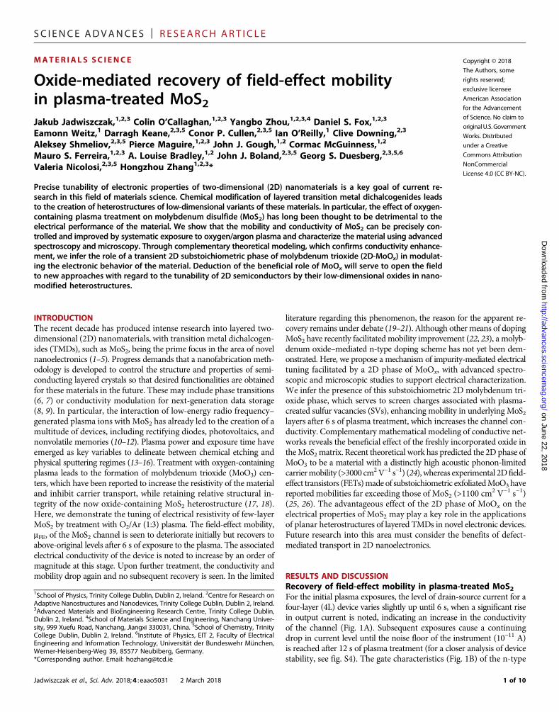
MoS2 surface modification by oxygen insertionWe use atomic force microscopy (AFM) to track the thickness var-iation and surface roughness of the plasma-treated flake. Phase mapsof the same region on a 4L flake are shown in Fig. 2 (A to C), withnotable change in contrast indicating material difference over time.Figure 2D charts the change in the edge heights evaluated from lineprofiles across the edges of the 4L and 5L regions (fig. S11). The ini-tial edge height on the 4L portion increases by ≈30% from 0 to 6 sand that on the 5L area increases by≈21%. This is followed by a sub-sequent drop in height for longer exposure times. This initial in-sertion agrees well with the expected height change if the top layerof MoS2 were to be replaced by a layer of a-MoO3 or MoOx with edge-sharing octahedra (29% for 4L and 23% for 5L). The surface rough-ness (Fig. 2E) may show a peak at 6 s owing to the formation of oxidepatches, but the average value does not vary more than the thicknessof one layer ofMoS2 orMoO3 in the first 8 s of exposure. The peak inedge height at 6 s is a critical point at which the etching mechanismshifts from one largely dominated by chemical oxygen insertion into
Jadwiszczak et al., Sci. Adv. 2018;4 : eaao5031 2 March 2018
the lattice to one where argon-dominated sputtering of material andremoval of species from the surface take over. With increasing dosesof the plasma, the integration of oxygen into the mechanically exfo-liated 2H-MoS2 structure will introduce considerable change, includingthe rearrangement of electronic density and effective lattice deforma-tion, which increases the interlayer distance. Oxygen intercalationbetween the top layer and the rest of the stack may also occur (28).All these factors lead to a rise in the thickness of the thin MoS2−xOx
film (14, 28–31) and can lead to rupturing (32) while forming oxide-containing patches on the surface at the same time. These fine oxidepatches, spectroscopically determined by Ko et al. (33) to exist, canbe seen in the scanning electron micrograph in Fig. 2G (for larger-scale images, see fig. S13). The contrast is due to the higher work func-tion of MoO3 (6.6 eV) (34) compared with that of MoS2 (≈4.04 to4.47 eV) (35). The structural modification undergone by theMoS2 inthe plasma chamber can also be linked to the change in its optical con-trast over time (see discussion in fig. S12). A recent study has shown thatsubstoichiometricMoO3−x can be volatile and even removed by Ar flowat low temperatures (36). In the O2/Ar plasma physical sputtering–dominated regime, the surface roughness is seen to increase by morethan 1 nm at 28 s of exposure due to Ar+-related etching and rede-position of material on the surface (15, 16). However, the unchangingsurface roughness up until 8 s indicates initial direct conversion ofMoS2 into a planar oxide. Most importantly, the edge height trendcorrelates with the electrical recovery discussed in the previous sec-tion, with a peak at 6 s.
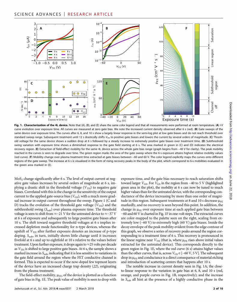
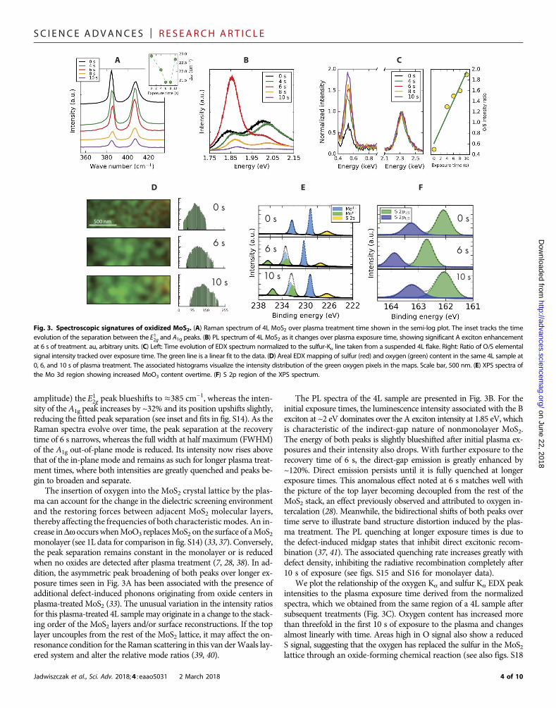
Spectroscopic analyses of the surface-bound oxideWe investigate the change to the chemical content of our MoS2 de-vices by using Raman, photoluminescence (PL), energy-dispersive x-ray(EDX), and x-ray photoelectron (XPS) spectroscopies. The offsetRaman spectra of the 4L flake (Fig. 3A) show notable shifts in thecharacteristic peaks corresponding to the A1g mode at ≈407 cm−1
and theE12g mode at≈384.5 cm−1 once the sample is exposed to the plas-
ma. After only 2 s of treatment (and accompanied by a decrease in
June 22, 2018
0 s 6 s 28 sA B
28 sFC
E
D
G
Fig. 2. Surface morphology of plasma-treated MoS2. (A to C) Phase maps of the same region of a 4L flake, showing notable material contrast on the surface asoxides are formed over time. Scale bars, 200 nm. (D) Chart of edge heights extracted along line profiles after each exposure time (see all the raw height maps in fig. S11).The region in green is the edge height peak, which correlates with the electrical recovery time at 6 s. (E) Root mean square (RMS) surface roughness profiles extracted overtime from height maps of the 4L and 5L regions of the flake. (F) AFM map of bottom edge of this flake after 28 s of plasma etching. Visible voids are seen along the bottomof the sample (G) scanning electron microscopy (SEM) image of the corner of the same flake, exhibiting dark contrast pits on the edge, corresponding to oxidizedMoS2 regions.
3 of 10
SC I ENCE ADVANCES | R E S EARCH ART I C L E
on June 22, 2018http://advances.sciencem
ag.org/D
ownloaded from
amplitude) the E12g peak blueshifts to ≈385 cm
−1, whereas the inten-sity of the A1g peak increases by ~32% and its position upshifts slightly,reducing the fitted peak separation (see inset and fits in fig. S14). As theRaman spectra evolve over time, the peak separation at the recoverytime of 6 s narrows, whereas the full width at half maximum (FWHM)of the A1g out-of-plane mode is reduced. Its intensity now rises abovethat of the in-plane mode and remains as such for longer plasma treat-ment times, where both intensities are greatly quenched and peaks be-gin to broaden and separate.
The insertion of oxygen into the MoS2 crystal lattice by the plas-ma can account for the change in the dielectric screening environmentand the restoring forces between adjacent MoS2 molecular layers,thereby affecting the frequencies of both characteristic modes. An in-crease inDw occurswhenMoO3 replacesMoS2 on the surface of aMoS2monolayer (see 1L data for comparison in fig. S14) (33, 37). Conversely,the peak separation remains constant in the monolayer or is reducedwhen no oxides are detected after plasma treatment (7, 28, 38). In ad-dition, the asymmetric peak broadening of both peaks over longer ex-posure times seen in Fig. 3A has been associated with the presence ofadditional defect-induced phonons originating from oxide centers inplasma-treated MoS2 (33). The unusual variation in the intensity ratiosfor this plasma-treated 4L samplemay originate in a change to the stack-ing order of the MoS2 layers and/or surface reconstructions. If the toplayer uncouples from the rest of the MoS2 lattice, it may affect the on-resonance condition for the Raman scattering in this van derWaals lay-ered system and alter the relative mode ratios (39, 40).
Jadwiszczak et al., Sci. Adv. 2018;4 : eaao5031 2 March 2018
The PL spectra of the 4L sample are presented in Fig. 3B. For theinitial exposure times, the luminescence intensity associated with the Bexciton at ~2 eV dominates over the A exciton intensity at 1.85 eV, whichis characteristic of the indirect-gap nature of nonmonolayer MoS2.The energy of both peaks is slightly blueshifted after initial plasma ex-posures and their intensity also drops. With further exposure to therecovery time of 6 s, the direct-gap emission is greatly enhanced by~120%. Direct emission persists until it is fully quenched at longerexposure times. This anomalous effect noted at 6 s matches well withthe picture of the top layer becoming decoupled from the rest of theMoS2 stack, an effect previously observed and attributed to oxygen in-tercalation (28). Meanwhile, the bidirectional shifts of both peaks overtime serve to illustrate band structure distortion induced by the plas-ma treatment. The PL quenching at longer exposure times is due tothe defect-induced midgap states that inhibit direct excitonic recom-bination (37, 41). The associated quenching rate increases greatly withdefect density, inhibiting the radiative recombination completely after10 s of exposure (see figs. S15 and S16 for monolayer data).
We plot the relationship of the oxygen Ka and sulfur Ka EDX peakintensities to the plasma exposure time derived from the normalizedspectra, which we obtained from the same region of a 4L sample aftersubsequent treatments (Fig. 3C). Oxygen content has increased morethan threefold in the first 10 s of exposure to the plasma and changesalmost linearly with time. Areas high in O signal also show a reducedS signal, suggesting that the oxygen has replaced the sulfur in the MoS2lattice through an oxide-forming chemical reaction (see also figs. S18
D FE
A CB
500 nm
Fig. 3. Spectroscopic signatures of oxidized MoS2. (A) Raman spectrum of 4L MoS2 over plasma treatment time shown in the semi-log plot. The inset tracks the timeevolution of the separation between the E12g and A1g peaks. (B) PL spectrum of 4L MoS2 as it changes over plasma exposure time, showing significant A exciton enhancement
at 6 s of treatment. au, arbitrary units. (C) Left: Time evolution of EDX spectrum normalized to the sulfur-Ka line taken from a suspended 4L flake. Right: Ratio of O/S elementalsignal intensity tracked over exposure time. The green line is a linear fit to the data. (D) Areal EDX mapping of sulfur (red) and oxygen (green) content in the same 4L sample at0, 6, and 10 s of plasma treatment. The associated histograms visualize the intensity distribution of the green oxygen pixels in the maps. Scale bar, 500 nm. (E) XPS spectra ofthe Mo 3d region showing increased MoO3 content overtime. (F) S 2p region of the XPS spectrum.4 of 10
SC I ENCE ADVANCES | R E S EARCH ART I C L E
onhttp://advances.sciencem
ag.org/D
ownloaded from
and S19 for monolayer data). Areal EDX mapping of the suspended4L MoS2 flake (Fig. 3D) suggests the insertion of oxygen into the MoS2structure in a patch-like pattern, as previously proposed (17, 42). Theassociated color histograms visualize the increased oxygen distributionin the sample with plasma time by increasing green pixel count origi-nating from the O elemental signal.
Figure 3E shows XPS spectra of the Mo 3d region, indicating theincreased presence of oxide species over exposure time. For the pris-tine sample, the peaks around 229 and 232 eV correspond to, respec-tively, the Mo4+ 3d5/2 and Mo4+ 3d3/2 spin-orbit split components.The 6-s spectrum shows a characteristic Mo6+ 3d doublet attributedto MoO3 (43). After 10 s of exposure, the intensity of the trioxide-associated doublet increases further, with a significant ratio of thesurface now containing MoO3 (estimated at 30 to 40% from areas ofeach fitted component). In addition, a thickogram calculation (44) re-veals that the intensity attenuation of the 10-s spectrum is consistent,within known parameters, with the presence of a bilayer of 2D-MoO3
(that is, a bulk unit cell of a-MoO3) on the surface at this exposure timeand 61% of the bilayer of 2D-MoO3 at 6 s (see calculation details insection S3 and Mo 4p, 4s spectra in fig. S22). In addition, the FWHMof the MoO3-associated doublets increases from the 6-s to the 10-sspectrum, suggesting the surface formation of amore stoichiometricallycomplete trioxide between 6 and 10 s of plasma treatment (see also theevidence of small peak originating from the S–Obond at 6 s in fig. S21).
Figure 3F demonstrates the S 2p region. Peak broadening is evi-dent with increased plasma exposure time, indicating a change in thechemical order of the surface. Substoichiometric MoS2−x has also beenreported to cause the characteristic broadening of the S 2p doublet (45),consistent with the picture of sulfur atoms being removed from the sur-face of the MoS2 flakes. Most interestingly, both the Mo 3d and S 2psignals are upshifted after 6 s and downshifted after 10 s in these spectra,which have been corrected to the C 1s core line (table S1). It is widely ac-cepted thatMoO3 can induce hole doping and concomitant downshift-ing of the MoS2 peaks due to Fermi level realignment (37, 42, 46, 47).This is in agreement with our transfer curves, with significant threshold
Jadwiszczak et al., Sci. Adv. 2018;4 : eaao5031 2 March 2018
voltage shift to positive gate biases at higher plasma exposure times(Fig. 1C). The upshift at 6 s may thus correlate with the n-type dopingobserved in the transfer curves in Fig. 1B.
All the above results demonstrate that the plasma-treated MoS2undergoes a continuing oxygen insertion and crystal structure dis-tortion. However, the full unit cell of plasma-generated MoO3 is aninsulator (17). The electrical recovery at the 6-s mark indicates thatan intermediary phase of substoichiometric MoO3 may exist betweenthe pristine MoS2 semiconductor and the MoO3-rich insulator, causingthe transient recovery of electrical properties within the exponentialdecay envelope known from the literature. This observed trend maysuggest the formation of a highly conductive form of MoOx recentlyreported in the literature (25, 26).
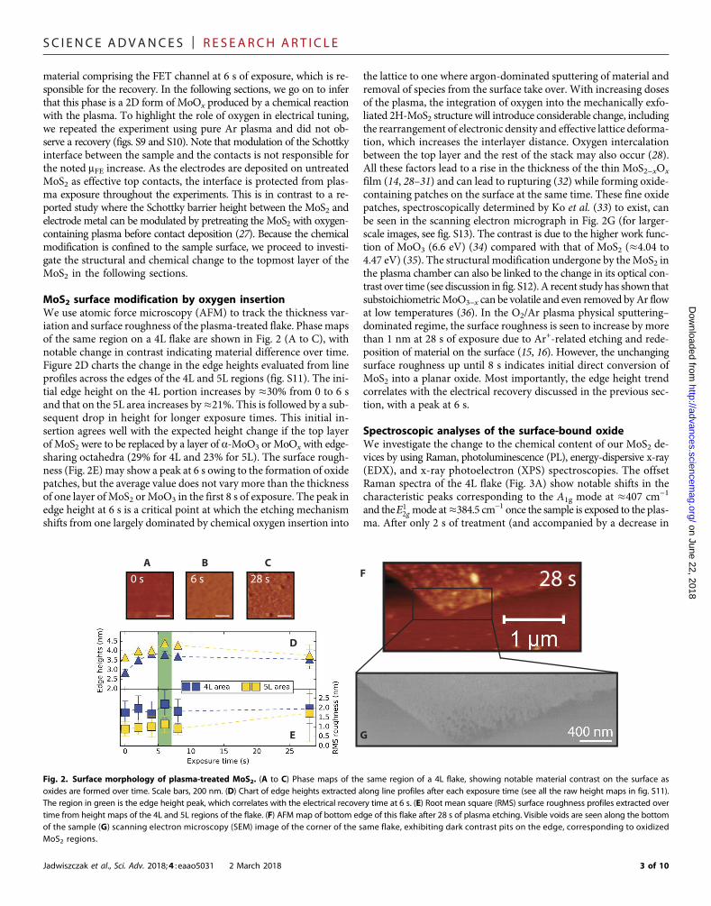
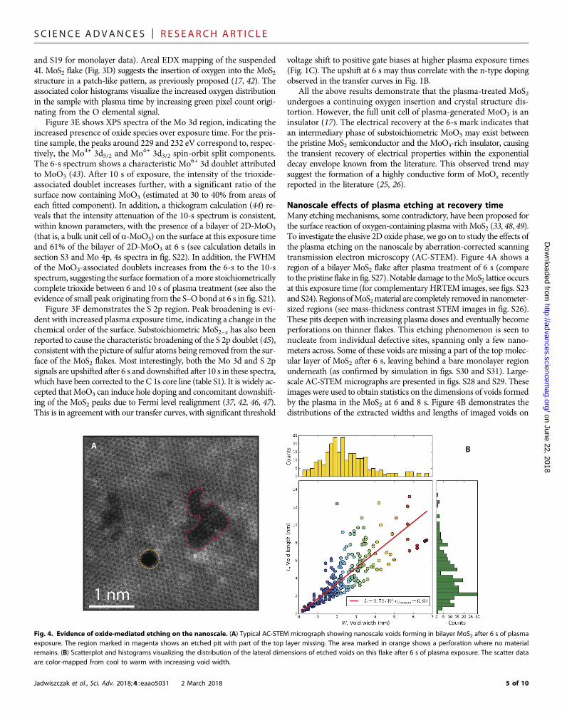
Nanoscale effects of plasma etching at recovery timeMany etching mechanisms, some contradictory, have been proposed forthe surface reaction of oxygen-containing plasma withMoS2 (33, 48, 49).To investigate the elusive 2D oxide phase, we go on to study the effects ofthe plasma etching on the nanoscale by aberration-corrected scanningtransmission electron microscopy (AC-STEM). Figure 4A shows aregion of a bilayer MoS2 flake after plasma treatment of 6 s (compareto the pristine flake in fig. S27). Notable damage to theMoS2 lattice occursat this exposure time (for complementary HRTEM images, see figs. S23andS24). RegionsofMoS2material are completely removed innanometer-sized regions (see mass-thickness contrast STEM images in fig. S26).These pits deepen with increasing plasma doses and eventually becomeperforations on thinner flakes. This etching phenomenon is seen tonucleate from individual defective sites, spanning only a few nano-meters across. Some of these voids are missing a part of the top molec-ular layer of MoS2 after 6 s, leaving behind a bare monolayer regionunderneath (as confirmed by simulation in figs. S30 and S31). Large-scale AC-STEMmicrographs are presented in figs. S28 and S29. Theseimages were used to obtain statistics on the dimensions of voids formedby the plasma in the MoS2 at 6 and 8 s. Figure 4B demonstrates thedistributions of the extracted widths and lengths of imaged voids on
June 22, 2018
A B
Fig. 4. Evidence of oxide-mediated etching on the nanoscale. (A) Typical AC-STEM micrograph showing nanoscale voids forming in bilayer MoS2 after 6 s of plasmaexposure. The region marked in magenta shows an etched pit with part of the top layer missing. The area marked in orange shows a perforation where no materialremains. (B) Scatterplot and histograms visualizing the distribution of the lateral dimensions of etched voids on this flake after 6 s of plasma exposure. The scatter dataare color-mapped from cool to warm with increasing void width.
5 of 10
SC I ENCE ADVANCES | R E S EARCH ART I C L E
on June 22, 2018http://advances.sciencem
ag.org/D
ownloaded from
the bilayer flake. Yellow (green) histograms show thewidth (length) dis-tributions. Length is here defined as the largest lateral void dimension,whereas width is the dimension perpendicular to it. A positive correla-tion between the lateral dimensions of the etched voids is extracted fromdata fitting (see residuals in fig. S32), showing the close-to-isotropicgrowth of the voids. The average area of a pore at 6 s is 12.5 ± 0.1 nm2
(see histograms in fig. S33). At this time, the relative total percentagearea covered by the voids from images sampled in the AC-STEM is≈3.6%. The distribution at 8 s is presented in fig. S34.
Markedly, the nanoscale EDX and electron energy-loss spectros-copy (EELS) mapping are performed with the 60 pm electron beamprobe return spectra, suggesting very little oxygen presence aroundthe recovery time (see spectra and discussion in fig. S20). It has beendemonstrated that oxygen plasma interaction with molybdenummetal leads to the creation of volatile Mo oxides (50), whereas a re-cent study has confirmed oxide volatility in oxidized MoS2 (36). Wefind that the plasma-formed oxide phase studied presently is volatileunder ultrahigh vacuum (UHV). When the sample is left overnightin the in situ testing system (~10−6 mbar), the n-type depletionmodefunctionality is reversed by a drastic shift ofVTH toward positive gatebiases (see fig. S8 for comparison with UHV-stable insulating MoO3).Similarly, when inserted into the vacuum chamber of the AC-STEMovernight (~10−9 mbar), the freestanding flakes lose their weakly boundsurface oxides. The inability to detect oxygen in these atomically re-solved voids leads us to infer that the oxide, which was present initiallyand is responsible for the electrical recovery, was sublimated underUHV conditions, leaving behind the underlying MoS2 structure.
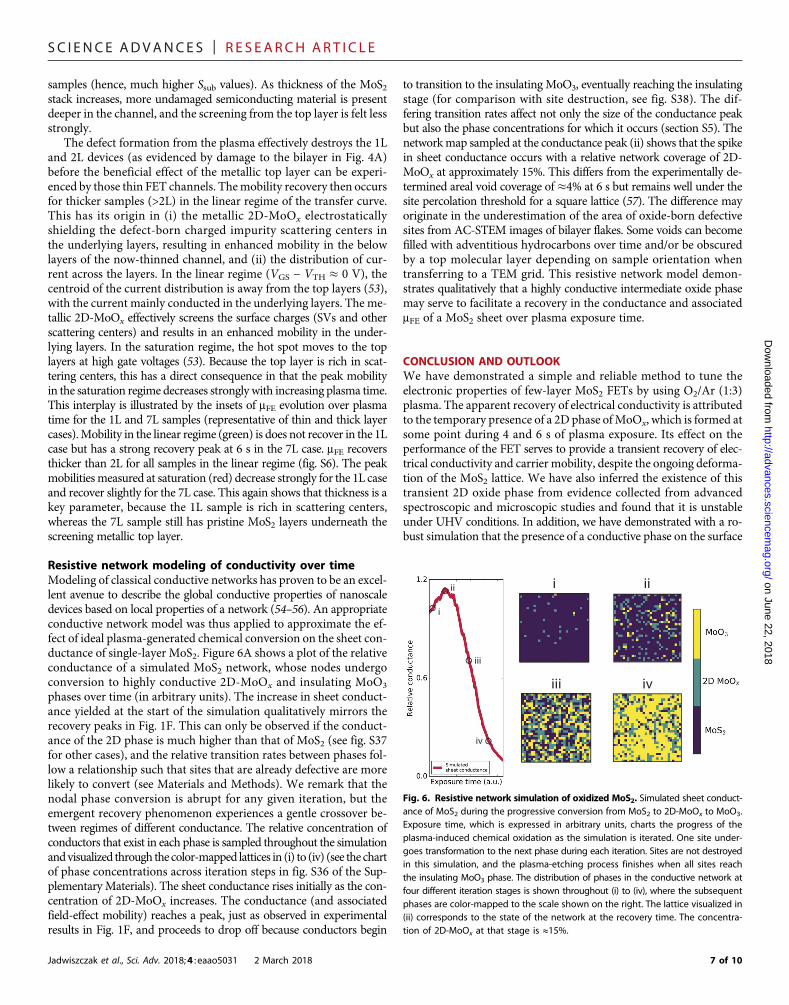
Dependence of mobility recovery on MoS2 layer numberTo obtain a more informed picture of how the oxide on the top layerof MoS2 affects the transport behavior of the FET, we fabricated andtested devices of different thicknesses between 1 and 10 layers in thesame fashion as the device in Fig. 1. The associated I-V curves, gatecurves, derived mobilities, and subthreshold swings at each plasmaexposure time are all collated in figs. S5 to S7. The highly consistentfeature of transfer curves at times when the 2D-MoOx is present onthe top layer is the drastic shift of threshold voltage to negative gatebiases. Figure 5A tracks DVTH for the tested MoS2 layer numbers.Here, DVTH is defined as the difference between the threshold volt-age before treatment and at the point of mobility recovery. Forsamples of all thicknesses, VTH shifts considerably to negative biasesby a similar amount, with the mean shift value of DVTH = −19 Vmarked on the plot by the horizontal yellow line. This behavioralconsistency and lack of dependence on layer number indicate the keyrole of the plasma-modified top surface layer. SVs are known to inducen-type doping and a negative VTH shift in MoS2 (51). Electrons willtransfer fromMoS2 to MoOx to equalize Fermi levels, but the numberof electrons transferred (52) isNe ≅ rmDE/e
2, where rm is themean sizeof oxide patches at 6 s seen inAC-STEM inFig. 4A andDE is the Fermienergy shift between the oxide and the MoS2. We calculate valuesof Ne, which are at least one order of magnitude smaller than the con-centration of SVs (the electron concentration being Cox DVTH/e ~1012 cm− 2). Hence, VTH will be largely shifted to negative gate biasesas plasma-created SVs strongly n-dope the FET channel at the pointof recovery. However, at longer plasma times, the oxide patches turninto insulating MoO3, which act as effective acceptors (47). At thesame time, the concentration of SVs decreases because they becomepreferential sites for oxygen incorporation. The vanishing of SVs andthe formation of hole-doping MoO3 eventually cause an imbalance
Jadwiszczak et al., Sci. Adv. 2018;4 : eaao5031 2 March 2018
to this interplay, resulting in a positive shift in VTH at longer plasmatimes (>10 s).
The effect of channel thickness on the screening effect of the me-tallic patches embedded in the top layer at recovery time can be wellunderstood by tracking the subthreshold swing variation for all thesamples over exposure time (fig. S7). In Fig. 5B, we plot the percent-age change of Ssub for MoS2 devices of all tested layer thicknesses(that is, a measure of how much Ssub increases at recovery time re-lative to no plasma treatment). The extracted data are well fitted withan asymptotic exponential function (R2 = 0.99). This demonstratesthe critical role that layer thickness plays in allowing the top metalliclayer to alter the field effect in the underlying MoS2 channel. Theconductivity of the metallic top layer is not tunable by the back gate(7). Hence, the on/off ratio at recovery time is severely reduced forsamples of all thicknesses, but this effect is felt more severely by thinner
B
A
Fig. 5. Effect of layer number on mobility recovery. (A) Change in gate thresh-old voltage between recovery time and pristine MoS2 tracked as a function oflayer number. Devices of all thicknesses show a major VTH shift to negative gatebias at the time of mobility recovery. The mean shift value of −19 V is marked bythe horizontal yellow line. (B) Percentage increase in subthreshold swing betweenuntreated and recovered stages for samples of all tested thicknesses. Ssub in-creases for all samples at the recovery stage and the effect scales with MoS2 layernumber. Insets track the mobility evolution over exposure time for the 1L and 7Lsamples in the linear (green) and saturation (red) regimes. The mobility recoveryhappens for samples thicker than two layers.
6 of 10
SC I ENCE ADVANCES | R E S EARCH ART I C L E
on June 22, 2018http://advances.sciencem
ag.org/D
ownloaded from
samples (hence, much higher Ssub values). As thickness of the MoS2stack increases, more undamaged semiconducting material is presentdeeper in the channel, and the screening from the top layer is felt lessstrongly.
The defect formation from the plasma effectively destroys the 1Land 2L devices (as evidenced by damage to the bilayer in Fig. 4A)before the beneficial effect of the metallic top layer can be experi-enced by those thin FET channels. Themobility recovery then occursfor thicker samples (>2L) in the linear regime of the transfer curve.This has its origin in (i) the metallic 2D-MoOx electrostaticallyshielding the defect-born charged impurity scattering centers inthe underlying layers, resulting in enhanced mobility in the belowlayers of the now-thinned channel, and (ii) the distribution of cur-rent across the layers. In the linear regime (VGS − VTH ≈ 0 V), thecentroid of the current distribution is away from the top layers (53),with the current mainly conducted in the underlying layers. The me-tallic 2D-MoOx effectively screens the surface charges (SVs and otherscattering centers) and results in an enhanced mobility in the under-lying layers. In the saturation regime, the hot spot moves to the toplayers at high gate voltages (53). Because the top layer is rich in scat-tering centers, this has a direct consequence in that the peak mobilityin the saturation regime decreases strongly with increasing plasma time.This interplay is illustrated by the insets of mFE evolution over plasmatime for the 1L and 7L samples (representative of thin and thick layercases).Mobility in the linear regime (green) is does not recover in the 1Lcase but has a strong recovery peak at 6 s in the 7L case. mFE recoversthicker than 2L for all samples in the linear regime (fig. S6). The peakmobilitiesmeasured at saturation (red) decrease strongly for the 1L caseand recover slightly for the 7L case. This again shows that thickness is akey parameter, because the 1L sample is rich in scattering centers,whereas the 7L sample still has pristine MoS2 layers underneath thescreening metallic top layer.
Resistive network modeling of conductivity over timeModeling of classical conductive networks has proven to be an excel-lent avenue to describe the global conductive properties of nanoscaledevices based on local properties of a network (54–56). An appropriateconductive network model was thus applied to approximate the ef-fect of ideal plasma-generated chemical conversion on the sheet con-ductance of single-layer MoS2. Figure 6A shows a plot of the relativeconductance of a simulated MoS2 network, whose nodes undergoconversion to highly conductive 2D-MoOx and insulating MoO3
phases over time (in arbitrary units). The increase in sheet conduct-ance yielded at the start of the simulation qualitatively mirrors therecovery peaks in Fig. 1F. This can only be observed if the conduct-ance of the 2D phase is much higher than that of MoS2 (see fig. S37for other cases), and the relative transition rates between phases fol-low a relationship such that sites that are already defective are morelikely to convert (see Materials and Methods). We remark that thenodal phase conversion is abrupt for any given iteration, but theemergent recovery phenomenon experiences a gentle crossover be-tween regimes of different conductance. The relative concentration ofconductors that exist in each phase is sampled throughout the simulationandvisualized through the color-mapped lattices in (i) to (iv) (see the chartof phase concentrations across iteration steps in fig. S36 of the Sup-plementary Materials). The sheet conductance rises initially as the con-centration of 2D-MoOx increases. The conductance (and associatedfield-effect mobility) reaches a peak, just as observed in experimentalresults in Fig. 1F, and proceeds to drop off because conductors begin
Jadwiszczak et al., Sci. Adv. 2018;4 : eaao5031 2 March 2018
to transition to the insulating MoO3, eventually reaching the insulatingstage (for comparison with site destruction, see fig. S38). The dif-fering transition rates affect not only the size of the conductance peakbut also the phase concentrations for which it occurs (section S5). Thenetworkmap sampled at the conductance peak (ii) shows that the spikein sheet conductance occurs with a relative network coverage of 2D-MoOx at approximately 15%. This differs from the experimentally de-termined areal void coverage of ≈4% at 6 s but remains well under thesite percolation threshold for a square lattice (57). The difference mayoriginate in the underestimation of the area of oxide-born defectivesites from AC-STEM images of bilayer flakes. Some voids can becomefilled with adventitious hydrocarbons over time and/or be obscuredby a top molecular layer depending on sample orientation whentransferring to a TEM grid. This resistive network model demon-strates qualitatively that a highly conductive intermediate oxide phasemay serve to facilitate a recovery in the conductance and associatedmFE of a MoS2 sheet over plasma exposure time.
CONCLUSION AND OUTLOOKWe have demonstrated a simple and reliable method to tune theelectronic properties of few-layer MoS2 FETs by using O2/Ar (1:3)plasma. The apparent recovery of electrical conductivity is attributedto the temporary presence of a 2D phase ofMoOx, which is formed atsome point during 4 and 6 s of plasma exposure. Its effect on theperformance of the FET serves to provide a transient recovery of elec-trical conductivity and carrier mobility, despite the ongoing deforma-tion of the MoS2 lattice. We have also inferred the existence of thistransient 2D oxide phase from evidence collected from advancedspectroscopic and microscopic studies and found that it is unstableunder UHV conditions. In addition, we have demonstrated with a ro-bust simulation that the presence of a conductive phase on the surface
i ii
iii iv
i
ii
iii
iv
x
Fig. 6. Resistive network simulation of oxidized MoS2. Simulated sheet conduct-ance of MoS2 during the progressive conversion from MoS2 to 2D-MoOx to MoO3.Exposure time, which is expressed in arbitrary units, charts the progress of theplasma-induced chemical oxidation as the simulation is iterated. One site under-goes transformation to the next phase during each iteration. Sites are not destroyedin this simulation, and the plasma-etching process finishes when all sites reachthe insulating MoO3 phase. The distribution of phases in the conductive network atfour different iteration stages is shown throughout (i) to (iv), where the subsequentphases are color-mapped to the scale shown on the right. The lattice visualized in(ii) corresponds to the state of the network at the recovery time. The concentra-tion of 2D-MoOx at that stage is ≈15%.
7 of 10
SC I ENCE ADVANCES | R E S EARCH ART I C L E
of MoS2 may induce a plasma dose-dependent recovery in the con-ductance of the material network. Our results are of great importanceto groups studying novel 2D TMDs and the fundamental propertiesof their low-dimensional oxides. In addition, the discovery of thisphenomenon has broad implications for future van der Waals hetero-structure devices and planar circuit architectures. Site-specific plasmamodification of MoS2 can be achieved by polymer protection, creat-ing oxide-rich regions that could operate at negative gate biases andserve as charge storage nodes and/or input valves into further circuitcomponents.
on June 22, 2018http://advances.sciencem
ag.org/D
ownloaded from
MATERIALS AND METHODSMoS2 exfoliation, identification, and transferMoS2 flakes were mechanically exfoliated from commercially avail-able bulk molybdenite crystals (SPI Supplies) using the adhesive tapemethod and deposited on a precleaned Si substrate capped by 285 nmof SiO2. Samples were identified through optical contrast measure-ments and Raman spectroscopy. Electron beam lithography (EBL)was used to define contacts, followed by deposition of metal film (5-nmTi/35-nm Au) and lift-off in acetone (see optical images of devices infig. S2). Suspended MoS2 samples were prepared using the stamp-transfer methodology (58) to move flakes from substrates onto TEMgrids by etching away the SiO2 surface underneath a polymer-embeddedMoS2 flake.
Plasma treatmentThe on-chip MoS2 FET devices were modified in a Fischione Instru-ments 1020 plasma cleaner (see specifications in fig. S1), producing a13.52-MHz field to ionize a 1:3 mixture of O2/Ar gas at a constantchamber pressure of ~5 mbar. The samples were always exposed tothe plasma for 2 s at a time, at the same position in the chamber (towithin ±1mm), to control the accuracy of the experiment. After eachexposure, the samples were removed and characterized electrically.
Electrical measurementsThe devices were globally back-gated through the highly doped Sisubstrate and measured in a two-probe configuration at a pressureof 10−4 mbar in the vacuum chamber of a SEM (see sketch of experi-mental geometry in fig. S3). The source and drain terminals were pro-vided by tungsten nanomanipulator tips (Imina miBot) connectingthe deposited contacts to anAgilent B2912Adual-channel sourcemeter.
MicroscopySamples were prescreened in a Zeiss Ultra microscope in STEM modeat 20 keV to determine appropriate thickness for further TEM andAC-STEM experiments (fig. S25). TEM was carried out in an FEI Titan80-300 operated at 300 keV at a chamber pressure of 4 × 10⁻⁷ mbar.AFM was performed at ambient pressure in an Oxford Asylum systemusing cantilevers calibrated at 140 kHz. AC-STEM was carried out ina Nion UltraSTEM 200 system operated at 60 keV, at a chamber pres-sure of ~10−9 mbar.
SpectroscopyBecause sampling efficiency from mechanically exfoliated flakes isextremely low, XPS was performed on larger bulk flakes, whose surface(≈2 mm2) was plasma-treated in the same way as all FET samples afterdeposition on Si/SiO2 substrates. The system used amonochromatedAl Ka x-ray source with an Omicron EA 125 hemispherical analyzer
Jadwiszczak et al., Sci. Adv. 2018;4 : eaao5031 2 March 2018
set to a pass energy of 19 eV, giving a combined instrumental andsource resolution of 0.50 eV. The spectra for these samples werefitted with 2H polytype peaks, as is usual for mechanically exfoliatedMoS2 flakes. PL spectroscopy was performed on substrate-supportedmonolayer flakes using an excitation wavelength of 405 nm. Ramanspectroscopy ofmonolayers was carried out at atmospheric pressure witha HORIBA Jobin Yvon 488-nm laser equipped with 1200 grooves/mmand a charge-coupled device camera. Acquisition time was fixed at10 acquisitions/s. A 100× objective lens was used. The laser spot sizewas ≈1 mm, whereas the power of the laser was kept below 1 mW.Raman/PL spectroscopy of 4L flakes was performed with a WITecAlpha 300R microscope using a 532-nm excitation laser, a spectralgrating of 1800 lines/mm, and a 100× microscope objective (numer-ical aperture, 0.95; spot size, ~0.3 mm). Spectra were taken with a la-ser power of less than 60 mWtominimize heating. EDXmapping wascarried out on suspended samples transferred onto TEM grids usingthe polymer stamp method (see the image in fig. S17) using a BrukerNano XFlash 5030 detector in a Zeiss Supra SEM at 5 keV, with a stepsize of 0.7 nm/pixel. Atomically resolved EELS and EDX maps wereacquired using the Nion microscope at 60 keV (for mapped regions,see fig. S35).
Simulation of conductive networksThe computational model begins with a resistive network of identicalconductors of magnitude gS2 = 1. During each iteration of the simula-tion, one random conductor transitions from its current phase to thenext phase with a certain probability, unless that conductor is alreadyin the final MoO3 phase. If it does not transition, then one of the adja-cent sites is chosen and the transition check process is repeated. Theprobabilities represent the differing transition rates that occur betweenphases. Although the transition rates are experimentally unknown, theassumption that they progress, such that (MoS2 → 2D-MoOx)p1 and(2D-MoOx → MoO3)p2, where p1 and p2 indicate relative conversionprobabilities for each process and p2 > p1, is made. This relationshipstems from the fact that the MoS2 basal plane is chemically unreactive,but any defective nucleation sites will more likely facilitate chemical re-actions once they are formed (59). The sheet conductance was thencalculated using Kirchhoff’s andOhm’s laws (section S5). The iterationswere continued until all conductors were in the insulatingMoO3 phase.Iterations in the simulation are a proxy to the plasma exposure time,with a certain number of phase transitions (or iterations) per unit time.We note that the phase conversion was instant and did not reflect thecrossover between conductance regimes on a localized scale but ratheron the scale of the whole network.
SUPPLEMENTARY MATERIALSSupplementary material for this article is available at http://advances.sciencemag.org/cgi/content/full/4/3/eaao5031/DC1section S1. Electrical characterization of MoS2 samplessection S2. Surface analysis and optical contrast changesection S3. Spectroscopysection S4. Scanning/transmission electron microscopysection S5. Simulation of conductive networksfig. S1. Cross section of the plasma cleaner (61).fig. S2. Optical micrographs of various MoS2 devices after EBL processing.fig. S3. Sketch of the experimental geometry.fig. S4. VTH consistency check: The electrical measurement has negligible effects on thetransfer curve of the sample without plasma treatment, with the threshold voltage notaffected by hysteresis at the used sweep rate of ~2 V/s.fig. S5. Full data set of electrical measurements for samples of all thicknesses.
8 of 10
SC I ENCE ADVANCES | R E S EARCH ART I C L E
on June 22, 2018http://advances.sciencem
ag.org/D
ownloaded from
fig. S6. Full data set of mobilities derived for samples of all thicknesses over plasma exposure time.fig. S7. Full data set of subthreshold swings derived for samples of all thicknesses over plasmaexposure time.fig. S8. The effect of keeping a plasma-tuned sample in SEM vacuum chamber overnight.fig. S9. Optical micrographs of a few-layer flake exposed to pure Ar plasma for several minutes.fig. S10. Effect of pure Ar plasma treatment on electrical properties.fig. S11. AFM height maps of the flake discussed in the main manuscript after 0, 2, 6, and 8 s ofplasma exposure (from top to bottom), with line profiles extracted from the marked edges.fig. S12. Visible drop in optical contrast of a 4L MoS2 flake after 28 s of plasma treatmentvisualized in the intensity drop of each individual RGB channel relative to the substrate.fig. S13. SEM images of the sample treated for 28 s, showing small pit-like visible regions ofdark contrast, as well as significant change to the material on the bottom edge of the flake.fig. S14. Fits of the MoS2 Raman peaks used to extract peak shifts in the 4L sample in themain manuscript.fig. S15. PL spectroscopy of plasma-treated monolayer MoS2.fig. S16. PL lifetime mapping of monolayer MoS2.fig. S17. Thin area of MoS2 contained in a poly(methyl methacrylate) stamp after transfer fromsubstrate onto the TEM grid.fig. S18. EDX spectroscopy of plasma-treated monolayer MoS2.fig. S19. EDX mapping of plasma-treated monolayer MoS2.fig. S20. EDX and EELS spectroscopy performed on plasma-treated samples in the AC-STEM.fig. S21. XPS spectral region highlighting the small presence of S-O bonding at 6 s oftreatment.fig. S22. XPS spectra of the Mo 4p, Mo 4s and Si 2s regions over plasma treatment time.fig. S23. HRTEM images (beam energy = 300 keV) of monolayer MoS2 after plasma exposurefor (from left) 0, 2, 5, 10, and 20 s.fig. S24. HRTEM images (beam energy = 300 keV) of few-layer MoS2 after plasma exposures for(from upper left reading to the right) 0, 4, 16, and 31 s.fig. S25. STEM images (beam energy = 20 keV) of few-layer MoS2 flakes taken in a SEM using atransmission detector.fig. S26. High-angle annular dark-field (HAADF) STEM images (beam energy = 300 keV inFEI TITAN) of same samples as in fig. S21; plasma-treated for 16 s.fig. S27. Medium-angle annular dark-field AC-STEM image (beam energy = 60 keV in NionUltraSTEM 200) of pristine bilayer MoS2 before any plasma treatment.fig. S28. HAADF AC-STEM images (beam energy = 60 keV in Nion UltraSTEM 200) of few-layerMoS2 plasma-treated for 6 s.fig. S29. HAADF AC-STEM images (beam energy = 60 keV in Nion UltraSTEM 200) of few-layerMoS2 plasma-treated for 8 s.fig. S30. Simulation of bilayer MoS2 with a peeled monolayer area and a perforated voidcarried out in QSTEM software.fig. S31. Comparison between experimentally imaged void and simulated bilayer region withtop layer removed.fig. S32. Close-to-normal distributions of residuals from data fits seen in Fig. 4B of the mainmanuscript, confirming goodness of linear fit.fig. S33. Histograms summarizing distribution of areas of etched pits after 6 and 8 s of plasmatreatment.fig. S34. Distribution of lateral sizes of voids after 8 s of etching.fig. S35. Mapping regions scanned in the Nion UltraSTEM 200 at 60 keV for locally resolvedspectroscopies of few-layer MoS2.fig. S36. Plot of concentration of the three phases in the simulation as they change withiteration number.fig. S37. Trial-and-error plots for different combinations of conductances between the threephases C1, C2, and C3.fig. S38. Comparison of simulated sheet conductance evolutions for schemes where sites aredestroyed/not destroyed.scheme S1. Cartoon of multilayer MoS2 sample being oxidized by Ar/O2 plasma from bothsides when the sample is suspended on a TEM grid.table S1. Peak shifts with exposure time for the Mo4+ 5/2 and Si 2s peaks relative to the C 1score line, indicating that shifts are due to doping and not substrate charging.References (60, 61)
REFERENCES AND NOTES1. B. Radisavljevic, A. Radenovic, J. Brivio, V. Giacometti, A. Kis, Single-layer MoS2 transistors.
Nat. Nanotechnol. 6, 147–150 (2011).2. B. Radisavljevic, A. Kis, Mobility engineering and a metal–insulator transition in
monolayer MoS2. Nat. Mater. 12, 815–820 (2013).3. D. Jariwala, V. K. Sangwan, L. J. Lauhon, T. J. Marks, M. C. Hersam, Emerging device
applications for semiconducting two-dimensional transition metal dichalcogenides.ACS Nano 8, 1102–1120 (2014).
4. D. Lembke, S. Bertolazzi, A. Kis, Single-layer MoS2 electronics. Acc. Chem. Res. 48, 100–110(2015).
Jadwiszczak et al., Sci. Adv. 2018;4 : eaao5031 2 March 2018
5. V. K. Sangwan, D. Jariwala, I. S. Kim, K.-S. Chen, T. J. Marks, L. J. Lauhon, M. C. Hersam,Gate-tunable memristive phenomena mediated by grain boundaries in single-layerMoS2. Nat. Nanotechnol. 10, 403–406 (2015).
6. Y.-C. Lin, D. O. Dumcenco, Y.-S. Huang, K. Suenaga, Atomic mechanism of thesemiconducting-to-metallic phase transition in single-layered MoS2. Nat. Nanotechnol.9, 391–396 (2014).
7. J. S. Kim, J. Kim, J. Zhao, S. Kim, J. H. Lee, Y. Jin, H. Choi, B. H. Moon, J. J. Bae,Y. H. Lee, S. C. Lim, Electrical transport properties of polymorphic MoS2. ACS Nano 10,7500–7506 (2016).
8. D. S. Fox, Y. Zhou, P. Maguire, A. O’Neill, C. Ó’Coileáin, R. Gatensby, A. M. Glushenkov,T. Tao, G. S. Duesberg, I. V. Shvets, M. Abid, M. Abid, H.-C. Wu, Y. Chen, J. N. Coleman,J. F. Donegan, H. Zhang, Nanopatterning and electrical tuning of MoS2 layers with asubnanometer helium ion beam. Nano Lett. 15, 5307–5313 (2015).
9. P. Cheng, K. Sun, Y. H. Hu, Memristive behavior and ideal memristor of 1T phase MoS2nanosheets. Nano Lett. 16, 572–576 (2016).
10. M. Chen, H. Nam, S. Wi, L. Ji, X. Ren, L. Bian, S. Lu, X. Liang, Stable few-layer MoS2rectifying diodes formed by plasma-assisted doping. Appl. Phys. Lett. 103, 142110 (2013).
11. S. Wi, H. Kim, M. Chen, H. Nam, L. J. Guo, E. Meyhofer, X. Liang, Enhancement ofphotovoltaic response in multilayer MoS2 induced by plasma doping. ACS Nano 8,5270–5281 (2014).
12. M. Chen, H. Nam, S. Wi, G. Priessnitz, I. M. Gunawan, X. Liang, Multibit data storage statesformed in plasma-treated MoS2 transistors. ACS Nano 8, 4023–4032 (2014).
13. N.-Y. Cui, N. M. D. Brown, A. McKinley, An AFM study of the topography of natural MoS2following treatment in an RF–oxygen plasma. Appl. Surf. Sci. 151, 17–28 (1999).
14. P. D. Fleischauer, Fundamental aspects of the electronic structure, materials properties andlubrication performance of sputtered MoS2 films. Thin Solid Films 154, 309–322 (1987).
15. J. B. Park, C. B. France, B. A. Parkinson, Scanning tunneling microscopy investigation ofnanostructures produced by Ar+ and He+ bombardment of MoS2 surfaces. J. Vac. Sci.Technol. B Nanotechnol. Microelectron. Mater. Process. Meas. Phenom. 23, 1532–1542 (2005).
16. D. Kim, H. Du, T. Kim, S. Shin, S. Kim, M. Song, C. Lee, J. Lee, H. Cheong, D. H. Seo, S. Seo,The enhanced low resistance contacts and boosted mobility in two-dimensionalp-type WSe2 transistors through Ar+ ion-beam generated surface defects. AIP Adv. 6,105307 (2016).
17. M. R. Islam, N. Kang, U. Bhanu, H. P. Paudel, M. Erementchouk, L. Tetard,M. N. Leuenberger, S. I. Khondaker, Tuning the electrical property via defect engineeringof single layer MoS2 by oxygen plasma. Nanoscale 6, 10033–10039 (2014).
18. S. I. Khondaker, M. R. Islam, Bandgap engineering of MoS2 flakes via oxygen plasma:A layer dependent study. J. Phys. Chem. C 120, 13801–13806 (2016).
19. K.-C. Chen, C.-R. Wu, X.-R. Chang, S.-W. Chang, S.-C. Lee, S.-Y. Lin, Enhancement offield-effect mobility in molybdenum-disulfide transistor through the treatment oflow-power oxygen plasma. Jpn. J. Appl. Phys. 55, 090302 (2016).
20. W. Yang, Q.-Q. Sun, Y. Geng, L. Chen, P. Zhou, S.-J. Ding, D. W. Zhang, The integrationof sub-10 nm gate oxide on MoS2 with ultra low leakage and enhanced mobility. Sci. Rep.5, 11921 (2015).
21. H. Nan, Z. Wu, J. Jiang, A. Zafar, Y. You, Z. Ni, Improving the electrical performance ofMoS2 by mild oxygen plasma treatment. J. Phys. D Appl. Phys. 50, 154001 (2017).
22. M.-Y. Ryu, H.-K. Jang, K. J. Lee, M. Piao, S.-P. Ko, M. Shin, J. Huh, G.-T. Kim, TriethanolaminedopedmultilayerMoS2 field effect transistors. Phys. Chem. Chem. Phys. 19, 13133–13139 (2017).
23. J. Guo, B. Yang, Z. Zheng, J. Jiang, Observation of abnormal mobility enhancement inmultilayer MoS2 transistor by synergy of ultraviolet illumination and ozone plasmatreatment. Physica E 87, 150–154 (2017).
24. W.-B. Zhang, Q. Qu, K. Lai, High-mobility transport anisotropy in few-layer MoO3 and itsorigin. ACS Appl. Mater. Interfaces 9, 1702–1709 (2017).
25. S. Balendhran, J. Deng, J. Z. Ou, S. Walia, J. Scott, J. Tang, K. L. Wang, M. R. Field, S. Russo,S. Zhuiykov, M. S. Strano, N. Medhekar, S. Sriram, M. Bhaskaran, K. Kalantar-Zadeh,Enhanced charge carrier mobility in two-dimensional high dielectric molybdenum oxide.Adv. Mater. 25, 108 (2013).
26. M. M. Y. A. Alsaif, A. F. Chrimes, T. Daeneke, S. Balendhran, D. O. Bellisario, Y. Son,M. R. Field, W. Zhang, H. Nili, E. P. Nguyen, K. Latham, J. van Embden, M. S. Strano, J. Z. Ou,K. Kalantar-zadeh, High-performance field effect transistors using electronic inks of 2Dmolybdenum oxide nanoflakes. Adv. Funct. Mater. 26, 91–100 (2016).
27. F. Giannazzo, G. Fisichella, G. Greco, S. Di Franco, I. Deretzis, A. La Magna, C. Bongiorno,G. Nicotra, C. Spinella, M. Scopelliti, B. Pignataro, S. Agnello, F. Roccaforte, AmbipolarMoS2 transistors by nanoscale tailoring of Schottky barrier using oxygen plasmafunctionalization. ACS Appl. Mater. Interfaces 9, 23164–23174 (2017).
28. R. Dhall, M. R. Neupane, D. Wickramaratne, M. Mecklenburg, Z. Li, C. Moore, R. K. Lake,S. Cronin, Direct bandgap transition in many-layer MoS2 by plasma-induced layerdecoupling. Adv. Mater. 27, 1573–1578 (2015).
29. V. Buck, Lattice parameters of sputtered MoS2 films. Thin Solid Films 198, 157–167 (1991).30. E. Schmidt, F. Weill, G. Meunier, A. Levasseur, New amorphous molybdenum oxysulfides
obtained in the form of thin films and their characterization by TEM. Thin Solid Films245, 34–39 (1994).
9 of 10
SC I ENCE ADVANCES | R E S EARCH ART I C L E
on June 22, 2018http://advances.sciencem
ag.org/D
ownloaded from
31. J. R. Lince, MoS2-xOx solid solutions in thin films produced by rf-sputter-deposition.J. Mater. Res. 5, 218–222 (1990).
32. R. Rao, A. E. Islam, P. M. Campbell, E. M. Vogel, B. Maruyama, In situ thermal oxidationkinetics in few layer MoS2. 2D Mater. 4, 025058 (2017).
33. T. Y. Ko, A. Jeong, W. Kim, J. Lee, Y. Kim, J. E. Lee, G. H. Ryu, K. Park, D. Kim, Z. Lee,M. H. Lee, C. Lee, S. Ryu, On-stack two-dimensional conversion of MoS2 into MoO3.2D Mater. 4, 014003 (2017).
34. Y. Guo, J. Robertson, Origin of the high work function and high conductivity of MoO3.
Appl. Phys. Lett. 105, 222110 (2014).35. S. Y. Lee, U. J. Kim, J. Chung, H. Nam, H. Y. Jeong, G. H. Han, H. Kim, H. M. Oh, H. Lee,
H. Kim, Y.-G. Roh, J. Kim, S. W. Hwang, Y. Park, Y. H. Lee, Large work function modulationof monolayer MoS2 by ambient gases. ACS Nano 10, 6100–6107 (2016).
36. T. N. Walter, F. Kwok, H. Simchi, H. M. Aldosari, S. E. Mohney, Oxidation and oxidativevapor-phase etching of few-layer MoS2. J. Vac. Sci. Technol. B Nanotechnol. Microelectron.Mater. Process. Meas. Phenom. 35, 021203 (2017).
37. N. Choudhary, M. R. Islam, N. Kang, L. Tetard, Y. Jung, S. I. Khondaker, Two-dimensionallateral heterojunction through bandgap engineering of MoS2 via oxygen plasma. J. Phys.Condens. Matter 28, 364002 (2016).
38. H. Zhu, X. Qin, L. Cheng, A. Azcatl, J. Kim, R. M. Wallace, Remote plasma oxidation andatomic layer etching of MoS2. ACS Appl. Mater. Interfaces 8, 19119–19126 (2016).
39. H. Li, Q. Zhang, C. C. R. Yap, B. K. Tay, T. H. T. Edwin, A. Olivier, D. Baillargeat, From bulk tomonolayer MoS2: Evolution of Raman scattering. Adv. Funct. Mater. 22, 1385–1390 (2012).
40. C. Lee, H. Yan, L. E. Brus, T. F. Heinz, J. Hone, S. Ryu, Anomalous lattice vibrations ofsingle- and few-layer MoS2. ACS Nano 4, 2695–2700 (2010).
41. N. Kang, H. P. Paudel, M. N. Leuenberger, L. Tetard, S. I. Khondaker, Photoluminescencequenching in single-layer MoS2 via oxygen plasma treatment. J. Phys. Chem. C 118,21258–21263 (2014).
42. A. T. Neal, R. Pachter, S. Mou, P-type conduction in two-dimensional MoS2 via oxygenincorporation. Appl. Phys. Lett. 110, 193103 (2017).
43. D. O. Scanlon, G. W. Watson, D. J. Payne, G. R. Atkinson, R. G. Egdell, D. S. L. Law,Theoretical and experimental study of the electronic structures of MoO3 and MoO2.
J. Phys. Chem. C 114, 4636–4645 (2010).44. P. J. Cumpson, The Thickogram: A method for easy film thickness measurement in XPS.
Surf. Interface Anal. 29, 403–406 (2000).45. M. A. Baker, R. Gilmore, C. Lenardi, W. Gissler, XPS investigation of preferential sputtering
of S from MoS2 and determination of MoSx stoichiometry from Mo and S peak positions.Appl. Surf. Sci. 150, 255–262 (1999).
46. S. McDonnell, A. Azcatl, R. Addou, C. Gong, C. Battaglia, S. Chuang, K. Cho, A. Javey,R. M. Wallace, Hole contacts on transition metal dichalcogenides: Interface chemistry andband alignments. ACS Nano 8, 6265–6272 (2014).
47. S. Chuang, C. Battaglia, A. Azcatl, S. McDonnell, J. S. Kang, X. Yin, M. Tosun, R. Kapadia,H. Fang, R. M. Wallace, A. Javey, MoS2 P-type transistors and diodes enabled by highwork function MoOx contacts. Nano Lett. 14, 1337–1342 (2014).
48. J. Yang, S. Kim, W. Choi, S. H. Park, Y. Jung, M.-H. Cho, H. Kim, Improved growth behaviorof atomic-layer-deposited high-k dielectrics on multilayer MoS2 by oxygen plasmapretreatment. ACS Appl. Mater. Interfaces 5, 4739–4744 (2013).
49. L. Tao, X. Duan, C. Wang, X. Duan, S. Wang, Plasma-engineered MoS2 thin-film as an efficientelectrocatalyst for hydrogen evolution reaction. Chem. Commun. 51, 7470–7473 (2015).
50. T. Saburi, H. Murata, T. Suzuki, Y. Fujii, K. Kiuchi, Oxygen plasma interactions with molybdenum:Formation of volatile molybdenum oxides. J. Plasma Fusion Res. 78, 3–4 (2002).
51. W. S. Leong, Y. Li, X. Luo, C. T. Nai, S. Y. Quek, J. T. L. Thong, Tuning the threshold voltage ofMoS2 field-effect transistors via surface treatment. Nanoscale 7, 10823–10831 (2015).
52. V. P. Zhdanov, nm-sized metal particles on a semiconductor surface, Schottky model, etc.Surf. Sci. 512, L331–L334 (2002).
53. S. Das, J. Appenzeller, Where does the current flow in two-dimensional layered systems?Nano Lett. 13, 3396–3402 (2013).
54. C. G. da Rocha, H. G. Manning, C. O’Callaghan, C. Ritter, A. T. Bellew, J. J. Boland,M. S. Ferreira, Ultimate conductivity performance in metallic nanowire networks.Nanoscale 7, 13011–13016 (2015).
Jadwiszczak et al., Sci. Adv. 2018;4 : eaao5031 2 March 2018
55. C. O’Callaghan, C. da Rocha, H. G. Manning, J. J. Boland, M. S. Ferreira, Effective mediumtheory for the conductivity of disordered metallic nanowire networks. Phys. Chem.Chem. Phys. 18, 27564–27571 (2016).
56. J. A. Fairfield, C. G. Rocha, C. O’Callaghan, M. S. Ferreira, J. J. Boland, Co-percolation totune conductive behaviour in dynamical metallic nanowire networks. Nanoscale 8,18516–18523 (2016).
57. T. Gebele, Site percolation threshold for square lattice. J. Phys. A Math. Gen. 17, L51(1984).
58. Y.-Q. Bie, Y.-B. Zhou, Z.-M. Liao, K. Yan, S. Liu, Q. Zhao, S. Kumar, H.-C. Wu,G. S. Duesberg, G. L. W. Cross, J. Xu, H. Peng, Z. Liu, D.-P. Yu, Site-specific transfer-printingof individual graphene microscale patterns to arbitrary surfaces. Adv. Mater. 23, 3938–3943(2011).
59. S. KC, R. C. Longo, R. M. Wallace, K. Cho, Surface oxidation energetics and kinetics onMoS2 monolayer. J. Appl. Phys. 117, 135301 (2015).
60. A. Ortiz-Conde, F. G. Sánchez, J. J. Liou, A. Cerdeira, M. Estrada, Y. Yue, A review of recentMOSFET threshold voltage extraction methods. Microelectron. Reliab. 42, 583–596(2002).
61. P. E. Fischione, J. Ringnada, Y. Feng, T. Krekels, M. Hayies, H. O. Colijn, M. J. Mills,J. M. Wiezorek, The use of a cold gas plasma for the final processing of contamination-free TEM specimens, in Specimen Preparation for Transmission Electron Microscopy ofMaterials IV, R. M. Anderson, S. D. Walck, Eds., (Materials Research Society SymposiaProceedings 480, 1997).
Acknowledgments: We are grateful to the staff at the Advanced Microscopy Laboratory,Centre for Research on Adaptive Nanostructures and Nanodevices (CRANN), Trinity CollegeDublin, for their continued technical support. We thank S. Callaghan for fruitful discussionsregarding XPS. Funding: The work at the School of Physics and CRANN at Trinity CollegeDublin was supported by Science Foundation Ireland (grant nos. 11/PI/1105, 12/TIDA/I2433,07/SK/I1220a, 12/IA/1482, and 08/CE/I1432) and the Irish Research Council (grant nos.GOIPG/2014/972, GOIPG/2013/680, and EPSPG/2011/239). C.P.C. and G.S.D. acknowledgesupport of Science Foundation Ireland under grant nos. 12/RC/2278 and 15/IA/3131. J.J.B.acknowledge support of European Research Council under grant no. 321160. Authorcontributions: J.J. analyzed the data, created the figures, and wrote the manuscript with inputfrom C.O. and H.Z. I.O. discovered the phenomenon. J.J. and Y.Z. conducted subsequentplasma exposures and electrical tests. C.O. and E.W. carried out the resistor network modeling.Y.Z. performed monolayer Raman experiments, whereas C.P.C. and J.J. performed 4LRaman experiments. P.M. and J.J. carried out SEM imaging and EDX measurements. D.S.F. andJ.J. performed HRTEM and STEM. C.D. acquired AC-STEM images and associated EELS andEDX maps. A.S. analyzed the AC-STEM results and performed QSTEM simulations. J.J., Y.Z.,and J.J.G. carried out the monolayer PL measurements. C.P.C. and J.J. collected the 4L PL data.C.M. and J.J. performed XPS experiments and analysis. D.K. and J.J. carried out AFMexperiments. M.S.F., G.S.D., A.L.B., J.J.B., V.N., and H.Z. oversaw the experimental work. H.Z.conceived the study and supervised the project. All authors have given approval for the finalversion of the manuscript. Competing interests: The authors declare that they have nocompeting interests. Data and materials availability: All data needed to evaluate theconclusions in the paper are present in the paper and/or the Supplementary Materials.Additional data related to this paper may be requested from H.Z. Raw data (code and source datafor graphs) generated and/or analyzed during the current study are available in the Zenodorepository at: DOI:10.5281/zenodo.1160542.
Submitted 28 July 2017Accepted 24 January 2018Published 2 March 201810.1126/sciadv.aao5031
Citation: J. Jadwiszczak, C. O’Callaghan, Y. Zhou, D. S. Fox, E. Weitz, D. Keane, C. P. Cullen,I. O’Reilly, C. Downing, A. Shmeliov, P. Maguire, J. J. Gough, C. McGuinness, M. S. Ferreira,A. L. Bradley, J. J. Boland, G. S. Duesberg, V. Nicolosi, H. Zhang, Oxide-mediated recovery offield-effect mobility in plasma-treated MoS2. Sci. Adv. 4, eaao5031 (2018).
10 of 10
2Oxide-mediated recovery of field-effect mobility in plasma-treated MoS
Louise Bradley, John J. Boland, Georg S. Duesberg, Valeria Nicolosi and Hongzhou ZhangO'Reilly, Clive Downing, Aleksey Shmeliov, Pierce Maguire, John J. Gough, Cormac McGuinness, Mauro S. Ferreira, A. Jakub Jadwiszczak, Colin O'Callaghan, Yangbo Zhou, Daniel S. Fox, Eamonn Weitz, Darragh Keane, Conor P. Cullen, Ian
DOI: 10.1126/sciadv.aao5031 (3), eaao5031.4Sci Adv
ARTICLE TOOLS http://advances.sciencemag.org/content/4/3/eaao5031
MATERIALSSUPPLEMENTARY http://advances.sciencemag.org/content/suppl/2018/02/26/4.3.eaao5031.DC1
REFERENCES
http://advances.sciencemag.org/content/4/3/eaao5031#BIBLThis article cites 60 articles, 0 of which you can access for free
PERMISSIONS http://www.sciencemag.org/help/reprints-and-permissions
Terms of ServiceUse of this article is subject to the
registered trademark of AAAS.is aScience Advances Association for the Advancement of Science. No claim to original U.S. Government Works. The title
York Avenue NW, Washington, DC 20005. 2017 © The Authors, some rights reserved; exclusive licensee American (ISSN 2375-2548) is published by the American Association for the Advancement of Science, 1200 NewScience Advances
on June 22, 2018http://advances.sciencem
ag.org/D
ownloaded from


![Plasma Reactor Coupled with Catalyst...temperature. Nader et al. [25] treated a mixed waste gas of benzene, toluene, and xylene with a synthesized catalyst and nonthermal plasma, e](https://static.fdocuments.us/doc/165x107/60e9e84b1a9293432b401905/plasma-reactor-coupled-with-catalyst-temperature-nader-et-al-25-treated.jpg)