OW-POWER PA MATCHING 1. Introduction
124
Rev. 0.3 12/12 Copyright © 2012 by Silicon Laboratories AN627-DS087 AN627 Si4060/Si4460/61 L OW -P OWER PA M ATCHING 1. Introduction This application note provides a description of the matching techniques applied to the low-power Si4060 TX and Si4460/61 TRX RFIC family. The typical power regime of the Si4461 is in the +13 to +16 dBm range, while the Si4060/Si4460 is primarily devoted to the +10–13 dBm applications. Specifically, this document does not address the matching procedure for the PA on the Si4063/4463/64 family of RFICs. Because the output power level on the Si4063/4463/64 family of RFICs is considerably higher than the Si4060/Si4460/61 RFIC, the matching procedure is somewhat different. The matching network achieves a number of goals simultaneously: Targets a nominal output power level of +10 to +16 dBm Minimizes current consumption (i.e., maximize efficiency) Constrains the peak voltage at the drain of the output devices Complies with ETSI and FCC specifications for spurious emissions Is immune against termination impedance variations as much as possible Has low variation over temperature and supply voltage Has low bill of materials and cost Unfortunately, not all of these goals can be satisfied in the most optimal way simultaneously. Silicon Labs investigates different matching types and methods to meet as much as possible with the above requirements. In this document, the best three TX matching types (the switched PA mode Class E (CLE) type, the switched PA mode square wave (SQW) type, and the Switched Current (SWC) type) are presented in detail. The main advantage of the switched mode (especially CLE) matching types is their very high efficiency. They are proposed for applications where the current consumption is most critical, e.g., the typical total chip current with CLE match (assuming 3.3 V Vdd) is ~17–19 mA at ~10 dBm, ~25 mA at ~13 dBm and ~40 mA at 16 dBm power levels. The SQW type match is proposed for use only at low frequencies (below 260 MHz, e.g. at 169 MHz), where the Class E operation is not efficient with the Pro IC family due to its low capacitance. The main disadvantage of the switching type PA matches is the high Vdd dependency (the power variation is proportional to the square of the Vdd change: i.e. dp = ~6 dB in the 1.8–3.8 V range) and the inaccurate nonlinear power steps. Also their current consumption and the peak voltage on the TX pin are sensitive to the termination impedance variation, and they usually require slightly higher order filtering and thus higher bill of materials cost. Some of these drawbacks can be cured to varying degrees with special methods that are described detailed later in this document. The main advantages of the SWC matches are the flat power vs. Vdd characteristic, better stability over temperature, accurate and linear power steps, simpler design process, and lower BOM costs due to the required weaker filtering. Therefore, the SWC match is proposed for applications in which the flat power characteristic and accurate power steps are the primarily concern and where the 10–20% higher current consumption is tolerated. However, the biggest disadvantage is the significantly worse efficiency compared to class E. Basically, the design can be tuned between better efficiency and better power flatness, i.e., by sacrificing efficiency, better power stability can be achieved. Typical current consumption of SWC matches tuned for high efficiency (and having worse flatness i.e. dp=~3 dB in the 1.8–3.8 V Vdd range) is 22–23 mA at 10 dBm and 30–32 mA at 13 dBm power levels. Typical current of flat power designs (dP=~1 dB in the 1.8–3.3 V Vdd range) is 24–25 mA at 10 dBm and 38 mA at 13 dBm power levels.
Transcript of OW-POWER PA MATCHING 1. Introduction

Rev. 0.3 12/12 Copyright © 2012 by Silicon Laboratories AN627-DS087
AN627
Si4060/Si4460/61 LOW-POWER PA MATCHING
1. Introduction
This application note provides a description of the matching techniques applied to the low-power Si4060 TX andSi4460/61 TRX RFIC family. The typical power regime of the Si4461 is in the +13 to +16 dBm range, while theSi4060/Si4460 is primarily devoted to the +10–13 dBm applications.
Specifically, this document does not address the matching procedure for the PA on the Si4063/4463/64 family ofRFICs. Because the output power level on the Si4063/4463/64 family of RFICs is considerably higher than theSi4060/Si4460/61 RFIC, the matching procedure is somewhat different.
The matching network achieves a number of goals simultaneously:
Targets a nominal output power level of +10 to +16 dBm
Minimizes current consumption (i.e., maximize efficiency)
Constrains the peak voltage at the drain of the output devices
Complies with ETSI and FCC specifications for spurious emissions
Is immune against termination impedance variations as much as possible
Has low variation over temperature and supply voltage
Has low bill of materials and cost
Unfortunately, not all of these goals can be satisfied in the most optimal way simultaneously. Silicon Labsinvestigates different matching types and methods to meet as much as possible with the above requirements. Inthis document, the best three TX matching types (the switched PA mode Class E (CLE) type, the switched PAmode square wave (SQW) type, and the Switched Current (SWC) type) are presented in detail.
The main advantage of the switched mode (especially CLE) matching types is their very high efficiency. They areproposed for applications where the current consumption is most critical, e.g., the typical total chip current withCLE match (assuming 3.3 V Vdd) is ~17–19 mA at ~10 dBm, ~25 mA at ~13 dBm and ~40 mA at 16 dBm powerlevels.
The SQW type match is proposed for use only at low frequencies (below 260 MHz, e.g. at 169 MHz), where theClass E operation is not efficient with the Pro IC family due to its low capacitance.
The main disadvantage of the switching type PA matches is the high Vdd dependency (the power variation isproportional to the square of the Vdd change: i.e. dp = ~6 dB in the 1.8–3.8 V range) and the inaccurate nonlinearpower steps.
Also their current consumption and the peak voltage on the TX pin are sensitive to the termination impedancevariation, and they usually require slightly higher order filtering and thus higher bill of materials cost.
Some of these drawbacks can be cured to varying degrees with special methods that are described detailed laterin this document.
The main advantages of the SWC matches are the flat power vs. Vdd characteristic, better stability overtemperature, accurate and linear power steps, simpler design process, and lower BOM costs due to the requiredweaker filtering. Therefore, the SWC match is proposed for applications in which the flat power characteristic andaccurate power steps are the primarily concern and where the 10–20% higher current consumption is tolerated.
However, the biggest disadvantage is the significantly worse efficiency compared to class E. Basically, the designcan be tuned between better efficiency and better power flatness, i.e., by sacrificing efficiency, better powerstability can be achieved.
Typical current consumption of SWC matches tuned for high efficiency (and having worse flatness i.e. dp=~3 dB inthe 1.8–3.8 V Vdd range) is 22–23 mA at 10 dBm and 30–32 mA at 13 dBm power levels.
Typical current of flat power designs (dP=~1 dB in the 1.8–3.3 V Vdd range) is 24–25 mA at 10 dBm and 38 mA at13 dBm power levels.

AN627
2 Rev. 0.3
Some of the switching type (CLE and SQW) disadvantages mentioned above can be cured to some extent byspecial methods.
For example, the high VDD variation can be cured efficiently at low power levels (e.g., 10 dBm with Si4060/Si4460or 14 dBm with Si4461), by the so-called adaptive power setting method. Since the low-power matches are usuallydesigned in such a way that the specified power at the specified supply voltage is achieved at a relatively lowpower level setting, at decreasing supply voltage (e.g., due to a discharging battery), the power drop can becompensated by the proper increase of the power level setting i.e., with the decrease of the switcher loss.Unfortunately, this method works well only at lower power regimes (+10 dBm with Si4060/Si4460 and +14 dBmwith Si4461) where a low power level setting is enough to get the targeted power, and, thus, there is room forcompensation. In these cases, the Class E stability over VDD can be even better than 1 dB in the 3.6–.2.1 V Vddrange.
A low power setting (at low power regimes) with higher switcher loss is also good to have immunity againsttermination antenna impedance variations. It especially reduces the variation of the dc current consumption withvariable environmental conditions suffered by the antenna, which is favorable for long-life battery-operatedapplications, such as meters or sensors, because the excess current drain is limited.
The operation type (CLE, SQW or SWC) can be set by the PA_MODE (0x2200) register. The 0x18 (Si4060/Si4460)and 0x20 (Si4461) values result in switching mode (CLE or SQW) operation, while the 0x19 (Si4060/Si4460) and0x21 (Si4461) values result in SWC operation.
In case of the switched PA mode (SQW and CLE) matches, the power can be set by the DDAC field in thePA_PWR_LVL (0x2201) register. The DDAC determines the number of used switching MOS fingers and thus theon-state resistance of the switcher.
In the case of SWC operation, the PA behaves like a high-impedance switched current generator; so, besides thenumber of fingers (DDAC), the delivered current per finger also determines the power. The current delivered by afinger can be set by the OB field of the PA_BIAS_CLKDUTY register in 10 µA steps.
Here, it is important to note that the critical output parasitic cap value of the PA does not depend on the number ofactive fingers (DDAC) as determined by the uppermost cascode MOS device connected to the TX pin.
It is theoretically possible to increase the efficiency of low-power CLE matches by reducing the current of theinternal PA drivers. For that, they can work in 25% duty cycle mode, by setting all bits of the CLK_DUTY field in thePA_BIAS_CLKDUTY register (0x2202) to 1, resulting in a PA_BIAS_CLKDUTY register value of 0xC0.
The 10 dBm and 13 dBm CLE matches with Si4060/Si4460 use this 25% duty cycler mode to save current. Thedrawback of this mode is the increased harmonic content and the consequently greater number of filteringcomponents.
With 50% duty cycle mode (PA_BIAS_CLKDUTY register is left in its default value of 0x00), the Si4060/Si4460high power (HP) CLE matches can achieve the 13–14 dBm power with sufficient margin, even with multilayerinductors. However, in this case, the current consumption will be nearly the same as it is with the Si4461 matches.Since the Si4461 has more robust PA, which is designed primarily to the 13–14 dBm power range, there is noreason to use the Si4060/61 ICs instead in 50% duty cycle CLE mode.
The matching procedure outlined in this document for CLE/SQW and SWC allows the user to achieve the abovementioned properties and is applicable for two different types of board configurations: one with separate antennasfor the TX and RX paths (Split TX/RX board configuration: in the case of TX only chips (Si4060) the TX path can beused by simply omitting the RX path) and one with a single antenna where the TX and RX paths are tied directlytogether without the use of an RF switch (Direct Tie board configuration: again, in case of TX only chips (Si4060),the TX path can be used and the Rx path can be omitted).
The differences in the matching procedure required for the two board configurations are discussed in detail.
The next chapter is provided for users more interested in quickly obtaining matching component values than in themethodology used to develop the matching network. The methodology is described in detail in Sections 3, 4, and 5.

AN627
Rev. 0.3 3
Table 1. Silicon Labs EZRadio Pro Sub-GHz Wireless IC Family RF Match Cross References
Match Type Advantages Disadvantages RF IC Types
Si4463/64 (TRX)
Si4461 (TRX) Si4460 (TRX)
Si4438 (TRX)
Si4063 (TX) Si4060 (TX) Si4362 (RX)
Class E Split High Efficiency, High Power
power varies with VDD, nonlinear
power steps
AN648, 868/915M 20 dBm &
85 mA
AN627, 434/868M
13–16 dBm & 26–43 mA
AN627, 434/868/
915M 10…13 dBm & 16–24 mA
AN732, 490 MHz, 20 dBm &
85 mA
AN648, 868/915M 20 dBm &
85 mA
AN627, 434/868/915M 10–13 dBm &
16–24 mA
—
Class E DT High Efficiency, High power, One antenna
power varies with VDD, nonlinear
power steps
AN648, 868/915M 20 dBm &
85 mA
AN627, 434/868M
13–16 dBm & 26.5–43 mA
AN627, 434/868/
915M 10–13 dBm & 17–25 mA
AN732, 490 MHz, 20 dBm &
85 mA
— — —
Class E TX/RX Switch
High Efficiency, One antenna
power varies with VDD, nonlinear
power steps, extra RF switch adds
cost
AN648, 868/915M 20 dBm &
85 mA
— — — — — —
SQW DT High Efficiency, High power, one antenna
power varies with VDD, nonlinear
power steps
AN648, 169M 20 dBm
& 70 mA
— AN627, 169M,
10 dBm & 18 mA
— — — —
SWC SPLIT Flat VDD characteristic, lower BOM (than class E),
linear power steps
less efficient, medium power
— AN627, 868/915M
13–14 dBm & 31–36 mA
AN627, 315/434/868/
915M 10 dBm &
24 mA
— — AN627, 315/434/868/ 915M 10 dBm
& 24 mA
—
SWC DT Flat VDD characteristic, lower BOM (than class E),
linear power steps, one antenna
less efficient, medium power
— AN627, 868/915M
13–14 dBm & 31–36 mA
AN627, 315/434/868/
915M 10 dBm &
24 mA
— — — —
4 Element RX Match
Balun with minimum phase and magnitude
error, fully matched
— — — — — — AN643, 10/13 mA

AN627
4 Rev. 0.3
TABLE OF CONTENTS
Section Page
1. Introduction . . . . . . . . . . . . . . . . . . . . . . . . . . . . . . . . . . . . . . . . . . . . . . . . . . . . . . . . . . . . .12. Summary of Matching Network Component Values . . . . . . . . . . . . . . . . . . . . . . . . . . . . .6
2.1. Component Values for Si4461 Matching . . . . . . . . . . . . . . . . . . . . . . . . . . . . . . . . . . .72.1.1. Si4461 with Split TX\RX SWC Board Configuration:
Component Values and Performance . . . . . . . . . . . . . . . . . . . . . . . . . . . . . . . .72.1.2. Si4461 with Direct Tie TX/RX SWC Board Configuration:
Component Values and Performance . . . . . . . . . . . . . . . . . . . . . . . . . . . . . . . .92.1.3. Si4461 CLE Split TX/RX Board Configuration:
Component Values and Performance . . . . . . . . . . . . . . . . . . . . . . . . . . . . . . .122.1.4. Si4461 CLE for Direct Tie Board Configuration:
Component Values and Performance . . . . . . . . . . . . . . . . . . . . . . . . . . . . . . .142.2. Component Values for Si4060/Si4460 Matchings . . . . . . . . . . . . . . . . . . . . . . . . . . .17
2.2.1. Si4060/Si4460 CLE Split TX/RX Board Configuration: Component Values and Performance . . . . . . . . . . . . . . . . . . . . . . . . . . . . . . .17
2.2.2. Si4460 CLE for Direct Tie Board Configuration: Component Values and Performance . . . . . . . . . . . . . . . . . . . . . . . . . . . . . . .19
2.2.3. Si4060/4460 with Split TX\RX SWC Board Configuration: Component Values and Performance . . . . . . . . . . . . . . . . . . . . . . . . . . . . . . .23
2.2.4. Si4460 with Direct Tie TX/RX SWC Board Configuration: Component Values and Performance . . . . . . . . . . . . . . . . . . . . . . . . . . . . . . .23
3. Switched Current (SWC) Matching Procedure Overview . . . . . . . . . . . . . . . . . . . . . . . .263.1. SCW Matching Design for Split TX/RX Boards . . . . . . . . . . . . . . . . . . . . . . . . . . . . .26
3.1.1. Measurement of PA Shunt Output Capacitance/Resistance (CPA/RPA) . . . .263.1.2. Selection/Calculation of RLOAD_INT . . . . . . . . . . . . . . . . . . . . . . . . . . . . . . .303.1.3. Calculation of PA Bias Current IPA . . . . . . . . . . . . . . . . . . . . . . . . . . . . . . . . .313.1.4. Calculation of Required ZLOAD at the TX Pin . . . . . . . . . . . . . . . . . . . . . . . .333.1.5. Transforming RANT into ZLOAD . . . . . . . . . . . . . . . . . . . . . . . . . . . . . . . . . .333.1.6. Verifying Initial TX Performance . . . . . . . . . . . . . . . . . . . . . . . . . . . . . . . . . . .343.1.7. Adding a Low-Pass Filter . . . . . . . . . . . . . . . . . . . . . . . . . . . . . . . . . . . . . . . .363.1.8. Final Split TX/RX Schematic . . . . . . . . . . . . . . . . . . . . . . . . . . . . . . . . . . . . . .393.1.9. Improved Efficiency at Lower Output Power Levels . . . . . . . . . . . . . . . . . . . .39
3.2. Overview of Matching Procedure for SWC Direct Tie Board . . . . . . . . . . . . . . . . . .403.2.1. Concept of Direct Tie Matching . . . . . . . . . . . . . . . . . . . . . . . . . . . . . . . . . . . .413.2.2. Construction of TX Match . . . . . . . . . . . . . . . . . . . . . . . . . . . . . . . . . . . . . . . .443.2.3. Calculate the Common Tie-Point Impedance . . . . . . . . . . . . . . . . . . . . . . . . .443.2.4. Construction of RX Match . . . . . . . . . . . . . . . . . . . . . . . . . . . . . . . . . . . . . . . .453.2.5. Direct Tie Connection of TX and RX Paths . . . . . . . . . . . . . . . . . . . . . . . . . . .483.2.6. Final Direct Tie Schematic . . . . . . . . . . . . . . . . . . . . . . . . . . . . . . . . . . . . . . .49
4. Class E (CLE) Matching Procedure Overview . . . . . . . . . . . . . . . . . . . . . . . . . . . . . . . . .504.1. Brief Overview of CLE Matching Procedure . . . . . . . . . . . . . . . . . . . . . . . . . . . . . . .504.2. Power Amplifier Circuit Description . . . . . . . . . . . . . . . . . . . . . . . . . . . . . . . . . . . . . .51

AN627
Rev. 0.3 5
4.3. Basic Switching PA Circuit Topology . . . . . . . . . . . . . . . . . . . . . . . . . . . . . . . . . . . .514.4. Theory of Operation of an Ideal Switching PA . . . . . . . . . . . . . . . . . . . . . . . . . . . . .534.5. Limitations of a Practical MOS Switching PA . . . . . . . . . . . . . . . . . . . . . . . . . . . . . .54
5. CLE Matching Procedure for the Si4060/Si4460/61 . . . . . . . . . . . . . . . . . . . . . . . . . . . . .565.1. Goals for the Matching Procedure . . . . . . . . . . . . . . . . . . . . . . . . . . . . . . . . . . . . . .56
5.1.1. Comments on Peak Drain Voltage Limit . . . . . . . . . . . . . . . . . . . . . . . . . . . . .565.1.2. Comments on Achieving the Targeted Output Power . . . . . . . . . . . . . . . . . . .56
5.2. Matching Procedure Overview . . . . . . . . . . . . . . . . . . . . . . . . . . . . . . . . . . . . . . . . .575.2.1. Split TX/RX Board Configuration . . . . . . . . . . . . . . . . . . . . . . . . . . . . . . . . . . .575.2.2. Single Antenna with Direct Tie Board Configuration . . . . . . . . . . . . . . . . . . . .57
5.3. Detailed Matching Procedure for Split TX/RX Board Configuration . . . . . . . . . . . . .585.3.1. Step #1: Select a Value for LCHOKE . . . . . . . . . . . . . . . . . . . . . . . . . . . . . . .585.3.2. Step #2: Choose/Calculate Values for the L0-C0 Series-Resonant Tank . . . .585.3.3. Step #3: Calculate the Required Value for ZLOAD . . . . . . . . . . . . . . . . . . . . .595.3.4. Step #4: Estimate the Required PA_PWR_LVL
Register Value from the Calculated Value of a Voltage-Limiting Resistor . . .605.3.5. Step #5: Calculate the Values for Matching Components LX and CX . . . . . .625.3.6. Step #6: Design a Low-Pass Filter . . . . . . . . . . . . . . . . . . . . . . . . . . . . . . . . .665.3.7. Summary of Match . . . . . . . . . . . . . . . . . . . . . . . . . . . . . . . . . . . . . . . . . . . . .76
5.4. Detailed Matching Procedure for Direct Tie Board Configuration . . . . . . . . . . . . . . .775.4.1. Steps #1–6: Same Design Procedure as for Split TX/RX
Board Configuration . . . . . . . . . . . . . . . . . . . . . . . . . . . . . . . . . . . . . . . . . . . .795.4.2. Step #7: Design RX Input Match . . . . . . . . . . . . . . . . . . . . . . . . . . . . . . . . . . .805.4.3. Step #8: Slightly Modify the Value of L0 . . . . . . . . . . . . . . . . . . . . . . . . . . . . .835.4.4. Summary of Match . . . . . . . . . . . . . . . . . . . . . . . . . . . . . . . . . . . . . . . . . . . . .86
Document Change List . . . . . . . . . . . . . . . . . . . . . . . . . . . . . . . . . . . . . . . . . . . . . . . . . . . .122Contact Information . . . . . . . . . . . . . . . . . . . . . . . . . . . . . . . . . . . . . . . . . . . . . . . . . . . . . . .124

AN627
6 Rev. 0.3
2. Summary of Matching Network Component Values
Some users are not greatly interested in the theoretical development of the matching network; rather, they areconcerned with quickly obtaining a set of component values for a given desired frequency of operation. For thoseusers, the resulting component values for the CLE, SQW and SWC PA matching network for multiple frequenciesand power levels across the operating range of the Si4060/Si4460 and Si4461 RFIC are summarized in thissection.
The matching networks may be realized with either wire-wound SMD inductors or multi-layer SMD inductors. Thecost of a multi-layer inductor is significantly lower than that of a wire-wound inductor, and, thus, in cost sensitiveapplications, the multi-layer solution is preferred. However, the performance of a circuit realization using only wire-wound inductors is generally better due to the higher Qs and lower ohmic losses than multi-layer inductors ofequivalent value. Due to the increased loss, a realization using multi-layer inductors typically requires a higherpower level setting and thus exhibits a slight increase in current consumption for the same amount of output power.
Also, multi-layer SMD inductors are often available only in coarser-spaced inductance values. It may cause ahigher deviation from the ideal class E values, especially in Direct Tie solutions where significant adjustments ofthe value of L0 are usually necessary in order to avoid degradation to RX sensitivity; this may be more difficult withonly the set of values available for a multi-layer series of inductors.
The component values shown in these tables are appropriate for a supply voltage of VDD = 3.3 V.
For other VDD voltages the 10 dBm Si4060/Si4460 and 14 dBm Si4461 CLE design needs adjustment of the PApower level (e.g., the previously-mentioned adaptive power control), which, to some extent, can compensate thepower variations. However, in case of 13–14 dBm Si4060/Si4460 and 16 dBm Si4461 CLE designs, the powersetting is close to maximum, and, thus, the margin for power degradation compensation at low supply voltagelevels is very limited.
The output power of a properly-matched SwC PA is relatively insensitive to the supply voltage changes; so, thecomponent values and the power level settings (DDAC and OB register fields) can be used for other values of VDDas well.
The matching networks are separated based on RFIC (Si4060/Si4460 and Si4461) types due to the different PAproperties.
The Si4461 PA has 127 MOS switching fingers so the DDAC register can go up to 0x7F. Its typical outputcapacitance is 2.5 pF independently of the DDAC setting due to its cascade architecture.
The Si4060/Si4460 PA has 79 MOS switching fingers; so, the DDAC register can go up to 0x4F. Its typical outputcapacitance is 1.25 pF independently of the DDAC setting due to its cascade architecture.
The component values shown in the following sections are appropriate when using 0402-size SMD components,such as the 0402HP-series of wire-wound inductors from CoilCraft, the LQG15HS-series of multi-layer inductorsfrom Murata, and the GRM15-series of ceramic capacitors from Murata. These values are appropriate for use onthe official Split TX/RX and Direct Tie reference board designs available on the Silicon Labs web site. Thepresented solutions are likely to operate satisfactorily with 0603-size SMD elements as well.
Surface-mount 0603-size or 0402-size components contain parasitic elements that modify their effective values atthe frequency of interest. Furthermore, it is convenient to use the nearest-available 5% or 10% component valuesrather than the exact component values predicted by, for example, filter design CAD software or filter prototypetables. Additionally, any printed circuit board layout has parasitics, such as trace inductance, component padcapacitance, etc.
This means that it will almost certainly be necessary to adjust the final matching values for the reader’s specificapplication and board layout. The above component values should be used as starting points and the valuesmodified slightly to zero-in on the best filter response and impedance match to 50 .

AN627
Rev. 0.3 7
2.1. Component Values for Si4461 MatchingThe Si4461 High Efficient SWC and CLE matches fit most for the 13–14 dBm power regime. At this power level,the CLE has enough margin to be stable over VDD with adaptive power control. The basic 13–14 dBm Si4461 SWCmatch is optimized for efficiency around 3.3 V. Despite, the power drop in the 1.8–3.6 V Vdd range is only 2–3 dB,much better than that of the CLE match. It has also linear power steps.
A second 868M SWC match optimized for flat power characteristic (dP=~1 dB) is also given in the tables below,but with higher current consumption.
The efficiency of the CLE solution is still significantly better than that of any SWC solution.
The 16 dBm regime can be achieved only with CLE matching. Unfortunately, as mentioned previously, it has highvariation over supply voltage because adaptive power control is no longer efficient due to the power setting here,which is close to the maximum.
2.1.1. Si4461 with Split TX\RX SWC Board Configuration: Component Values and Performance
Table 2 provides the component values required for output power levels of both +13 and +14 dBm, using the SplitSWC TX/RX board configuration of Figure 1 and a supply voltage of VDD = 3.3 V. The matches described inTable 2 are optimized for the best efficiency and use wire-wound type inductors. At the time of this writing, noSi4461 SWC split match with multilayer inductors are fully tested, but the matches given in Table 2 give satisfactoryresults with multilayer inductors as well (if an inductor value does not exist, use the closest one). Some tuning(slight increase on OB and/or DDAC value) of the power setting and/or the element values may required here. Forother frequencies not given here, consult with a Silicon Labs representative.
If a flat Si4461 SWC TX only/split solution is required, use the TX part of the flat DT SWC match given in Table 4 onpage 9.
Table 2. TX Matching Network Component Values vs. Frequency (Split Si4460 High-Efficiency SWC TX/RX Board, VDD=3.3 V, Tested with Wire-Wound Inductors)
Freq Band Lchoke C0 LM1 CM1 LM2 CM2 LM3
Pout = +13 dBm
868 MHz 120 nH 47 pF 18 nH 5.1 pF 13.0 nH 3.9 pF 0
915 MHz 100 nH 39 pF 16 nH 5.1 pF 12.0 nH 3.9 pF 0
Pout = +14 dBm
868 MHz 120 nH 47 pF 16 nH 5.1 pF 13.0 nH 3.9 pF 0
915 MHz 100 nH 39 pF 15 nH 5.1 pF 12.0 nH 3.9 pF 0
AN627
8 Rev. 0.3
Figure 1. TX Matching Topology for Split SWC TX/RX Board Configuration
Table 3 lists summary of typical measured output power and current consumption for split board configurationsgiven in Figure 1 and in Table 3. These results are obtained with a supply voltage of VDD = 3.3 V and with wire-wound inductors.
Table 3. Output Power and Current Consumption vs. Frequency (Split Si4461 High-Efficiency SWC TX/RX Board, VDD = 3.3 V, Tested with Wire-Wound Inductors)
Freq Band OB[5:0] DDAC[6:0] Pout (dBm) IDC (mA)
Pout = +13 dBm
868 MHz 0x21 0x64 12.96 dBm 30.56 mA
915 MHz 0x22 0x64 12.85 dBm 30.15 mA
Pout = +14 dBm
868 MHz 0x2C 0x64 14.10 dBm 35.61 mA
915 MHz 0x2E 0x64 14.01 dBm 36.10 mA

AN627
Rev. 0.3 9
2.1.2. Si4461 with Direct Tie TX/RX SWC Board Configuration: Component Values and Performance
Table 4 provides the component values required for output power levels of both +13 and +14 dBm using the SingleAntenna with Direct Tie SWC board configuration of Figure 2 and a supply voltage of VDD = 3.3 V. One part ofthese matches is optimized for the best efficiency (denoted by HE in Table 4) and thus has 2–3 dB power variationin the 1.8–3.8 V Vdd range. It is still significantly better than the flatness of any CLE match.
At 868M there is also a second, flat Vdd characteristic SWC DT proposal (denoted by FC). This has 1.5 dB powervariation in the 1.8–3.8 V Vdd range (see Table 7). At the time of this writing, these 4461 SWC DT matches werenot tested with multilayer inductor yet. Consult with a Silicon Labs representative for other frequency SWCmatches.
A summary of typical measured output power, current consumption, and sensitivity (40 kbps, dev = 50 kHz (H = 1),0.1% BER) for high efficiency (denoted by HE) and a 868M flat (FC) SWC direct tie board configurations of Table 4are shown in Table 5. These results are obtained with a supply voltage of VDD = 3.3 V.
Table 4. Matching Network Component Values vs. Frequency (Direct Tie Si4461 SWC Board, VDD = 3.3 V, Tested with Wire-Wound Inductors)
Pout = +13 dBm
Freq Band
RX Side TX Side
LR1 LR2 CR1 CR2 Lchoke C0 LM1 CM1 LM2 CM2 LM3 CM3
HE868M 20 nH 24 nH 3.0 pF 1.0 pF 120 nH 47 pF 18 nH 5.1 pF 13 nH 3.9 pF 0 N.F
HE915M 18 nH 22 nH 3.0 pF 1.0 pF 100 nH 39 pF 16 nH 5.1 pF 12 nH 3.9 pF 0 N.F.
FC868M 16 nH 16 nH 3.6 pF 1.5 pF 120 nH 47 pF 8 nH 8.2 pF 8 nH 8.2 pF 7.5 nH 3.9 pF
Pout = +14 dBm
Freq Band
RX Side TX Side
LR1 LR2 CR1 CR2 Lchoke C0 LM1 CM1 LM2 CM2 LM3 CM3
HE868M 20 nH 24 nH 3.0 pF 1.0 pF 120 nH 47 pF 16 nH 5.1 pF 13 nH 3.9 pF 0 N.F.
HE915M 18 nH 22 nH 3.0 pF 1.0 pF 100 nH 39 pF 15 nH 5.1 pF 12 nH 3.9 pF 0 N.F.
Table 5. Output Power, Current Consumption and Sensitivity vs. Frequency (Direct Tie Si4461 SWC Board, VDD = 3.3 V, Tested with Wire-Wound Inductors)
Pout = +13 dBm
Freq Band OB[5:0] DDAC[6:0] Pout (dBm) IDC (mA) Sens. (dBm)
HE868M 0x20 0x64 12.77 dBm 30.62 mA –109.0 dBm
HE915M 0x20 0x64 12.79 dBm 30.23 mA –108.8 dBm
FC868M 0x27 0x7F 13.00 dBm 38.00 mA –108.3 dBm

AN627
10 Rev. 0.3
At all frequencies, the RX sensitivities achieved with the Direct Tie board configuration are within 1.5 dB of thoseobtained with the Split TX/RX board configuration. The power vs. Vdd characteristic is given for the 868M flat(FC868M) DT design in Table 6.
Pout = +14 dBm
HE868M 0x2D 0x64 13.86 dBm 35.97 mA –109.0 dBm
HE915M 0x2C 0x64 13.99 dBm 35.60 mA –108.8 dBm
Table 6. Output Power, Current Consumption vs. Vdd (Direct Tie Si4461 flat SWC Board, Wire Wound Inductors)
Vdd [V] FC868M PA_BIAS = 0x27, PA_PWR_LVL = 0x7F
Pout [dBm] Idc [mA]
1.8 11.7 34
2.1 12.5 35.6
2.4 12.8 37
2.7 12.9 37.5
3 13.1 38
3.3 13 38
3.6 13 38
3.8 13 38
delta (2.1–3.3 V) 0.5 2.4
delta (1.8–3.8 V) 1.4 4
Table 5. Output Power, Current Consumption and Sensitivity vs. Frequency (Direct Tie Si4461 SWC Board, VDD = 3.3 V, Tested with Wire-Wound Inductors) (Continued)

AN627
Rev. 0.3 11
Figure 2. Matching Topology for Single Antenna with Direct Tie SWC Board Configuration

AN627
12 Rev. 0.3
2.1.3. Si4461 CLE Split TX/RX Board Configuration: Component Values and Performance
Table 7 lists the component values required for output power levels for +14 and +16 dBm using the Split CLE TX/RX board configuration of Figure 3 and a supply voltage of VDD = 3.3 V. Table 7 matching is proper for both wire-wound and multilayer type inductors. For other frequencies, consult with a Silicon Labs representative.
Figure 3. TX Matching Topology for Si4461 Split TX/RX Board CLE Configuration
Table 7. TX Matching Network Component Values vs. Frequency (Split Si4461 CLE TX/RX Board, VDD = 3.3 V, Wire-Wound and Multilayer Inductor Versions)
Freq Band
Lchoke C0 L0 CM LM CM2 LM2 CM3 LM3 RDC
Pout = +14 dBm
434 MHz 220 nH 15 pF 39 nH 8.2 pF 18 nH 15 pF 18 nH 6.8 pF 0 0
868 MHz 120 nH 22.0 pF 12.0 nH 4.7 pF 8.2 nH 3.9 pF 0 N.F. 0 0
Pout = +16 dBm
434 MHz 220 nH 8.2 pF 39 nH 8.2 pF 18 nH 15 pF 18 nH 6.8 pF 0 0
868 MHz 120 nH 22.0 pF 10.0 nH 4.7 pF 8.2 nH 3.9 pF 0 N.F. 0 0

AN627
Rev. 0.3 13
A summary of typical measured output power and current consumption for split board configurations (both withwire-wound and multilayer inductors) is given in Table 8. These results are obtained with a supply voltage ofVDD = 3.3 V.
In the case of WW inductors, a lower power state setting is enough for the same output power due to the lowerloss. Due to the lower power setting, the WW solution is more robust against supply voltage variations withadaptive power control. In addition, it is more robust against-load impedance variations. The efficiency is alsobetter compared to the Multilayer matches. Moreover, with some slight component value adjustments (basically, ofC0 and CM), the WW solutions can be tuned for slightly better efficiency (~2…5%) with a simultaneous sacrifice ofrobustness.
Table 8. Output Power and Current Consumption vs. Frequency (Split Si4461 CLE TX/RX Board, VDD = 3.3 V, Wire-Wound (WW) and Multilayer (ML) Inductor)
Freq Band DDAC[6:0] WW
Pout WW (dBm)
IDC WW (mA) DDAC[6:0] ML
Pout ML (dBm)
IDC ML (mA)
Pout = +14 dBm
434 MHz 20h 14.3 dBm 28.1 mA 2Dh 14.3 dBm 29.7 mA
868 MHz 2Bh 14.4 dBm 31.6 mA 34h 14.3 dBm 34.4 mA
Pout = +16 dBm
434 MHz 32h 16.3 dBm 35.8 mA 7Fh 16.3 dBm 38.9 mA
868 MHz 40h 16.3 dBm 38.9 mA 4Fh 16.2 dBm 42.7 mA
AN627
14 Rev. 0.3
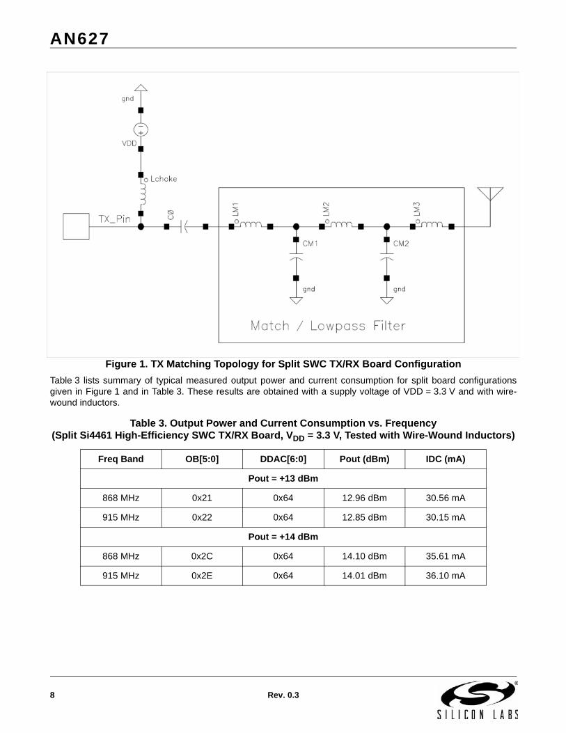
2.1.4. Si4461 CLE for Direct Tie Board Configuration: Component Values and Performance
Table 9 (wire-wound inductor) and Table 10 (multilayer inductor) provide the component values required for outputpower levels of both +14 and +16 dBm using the Single Antenna with Direct Tie board configuration of Figure 4and a supply voltage of VDD = 3.3 V. For other frequencies, consult with a Silicon Labs representative.
A summary of typical measured output power, current consumption, and sensitivity in RX mode (100 kbps, H = 1,0.1% BER) for direct tie board configurations and circuit realizations is shown in Table 11. These results areobtained with a supply voltage of VDD = 3.3 V. The multilayer inductor version has worse efficiency.
Table 9. Matching Network Component Values vs. Frequency (Direct Tie Si4461 CLE Board, VDD = 3.3 V, Wire-Wound Inductor)
Pout = +14 dBm
Freq Band
RX Side TX Side
LR1 LR2 CR1 CR2 Lchoke C0 L0 CM LM CM2 LM2 CM3 RDC
434 MHz 56 nH 51 nH 3.9 pF 2.2 pF 220 nH 15 pF 39 nH 8.2 pF 18 nH 15 pF 18 nH 6.8 pF 0
868 MHz 20 nH 24 nH 3.0 pF 1.0 pF 120 nH 22 pF 8.2 nH 5.6 pF 6.8 nH 5.6 pF 0 N.F. 0
Pout = +16 dBm
Freq Band
RX Side TX Side
LR1 LR2 CR1 CR2 Lchoke C0 L0 CM LM CM2 LM2 CM3 RDC
434 MHz 56 nH 51 nH 3.9 pF 2.2 pF 220 nH 15.0 pF 39 nH 8.2 pF 18 nH 15 pF 18 nH 6.8 pF 0
868 MHz 20 nH 24 nH 3.0 pF 1.0 pF 120 nH 22 pF 8.2 nH 5.6 pF 6.8 nH 5.6 pF 0 N.F. 0
Table 10. Matching Network Component Values vs. Frequency (Direct Tie Si4461 CLE Board, VDD = 3.3 V, Multilayer Inductor)
Pout = +14 dBm
Freq Band
RX Side TX Side
LR1 LR2 CR1 CR2 Lchoke C0 L0 CM LM CM2 LM2 CM3 RDC
434 MHz 56 nH 56 nH 5.1 pF 2.7 pF 220 nH 15 pF 39 nH 8.2 pF 18 nH 15 pF 18 nH 6.8 pF 0
868 MHz 18 nH 22 nH 3.0 pF 1.2 pF 120 nH 22 pF 8.2 nH 5.6 pF 6.8 nH 5.6 pF 0 N.F. 0
Pout = +16 dBm
Freq Band
RX Side TX Side
LR1 LR2 CR1 CR2 Lchoke C0 L0 CM LM CM2 LM2 CM3 RDC
434 MHz 56 nH 56 nH 5.1 pF 2.7 pF 220 nH 8.2 pF 39 nH 8.2 pF 18 nH 15 pF 18 nH 6.8 pF 0
868 MHz 18 nH 22 nH 3.0 pF 1.2 pF 120 nH 22 pF 8.2 nH 5.6 pF 6.8 nH 5.6 pF 0 N.F. 0

AN627
Rev. 0.3 15
At all frequencies, the RX sensitivities achieved with the Direct Tie board configuration are within 2 dB of thoseobtained with the Split TX/RX board configuration.
Table 11. Output Power, Current Consumption and RX Sensitivity vs. Frequency (Direct Tie Si4461 CLE Board, VDD = 3.3 V, Wire-Wound (WW) and Multilayer (ML) Inductors)
Freq Band DDAC[6:0] WW
Pout WW (dBm)
IDC WW (mA)
Sens WW (dBm)
DDAC[6:0] ML
Pout ML (dBm)
IDC ML (mA)
Sens ML (dBm)
Pout = +14 dBm
434 MHz 21h 14.4 dBm 28.7 mA –104.7 dBm 2Fh 14.3 dBm 30.1 mA –103.7 dBm
868 MHz 2Eh 14.3 dBm 33.2 mA –103.5 dBm 34h 14.3 dBm 34.4 mA –101.3 dBm
Pout = +16 dBm
434 MHz 3Fh 16.3 dBm 33.0 mA –104.7 dBm 7Fh 16.4 dBm 40.1 mA –104.0 dBm
868 MHz 41h 16.3 dBm 39.6 mA –103.5 dBm 5Eh 16.3 dBm 42.9 mA –101.3 dBm

AN627
16 Rev. 0.3
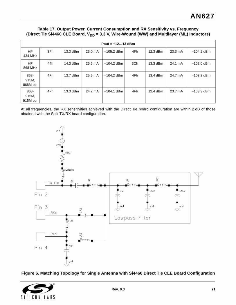
Figure 4. Matching Topology for Single Antenna with Si4461 Direct Tie CLE Board Configuration

AN627
Rev. 0.3 17
2.2. Component Values for Si4060/Si4460 MatchingsThe Si4060/Si4460 CLE, SQW, and SWC types are typically proper for 10 dBm applications, where they haveeither good efficiency (CLE match with 17–19 mA total current) or stable operation (a SWC match designed for flatpower characteristic has a power variation ~1 dB in the 1.8–3.8 V Vdd range). For flat Vdd characteristic (1–2 dBpower variation), the CLE needs adaptive power control.
The 13 to 14 dBm regime can only be achieved with CLE matching. It has high variation over Vdd, even withadaptive power control, because it is no longer efficient due to the power setting here, which is close to themaximum. Also, with this high power, the CLE matching is sensitive to the termination impedance variations. Theonly advantage of these high-power Si4460 CLE matchings is the good efficiency.
It must be noted that all Si4060/Si4460 CLE matches are working in 25% duty cycle mode to achieve the bestefficiency (PA_BIAS_CLKDUTY register is set to 0xC0).
The 13 dBm power CLE Si4060/4460 matches could work better with a 50% duty cycle, with a lower power state,i.e., with more margin. But, in this case, the current consumption would be also higher, and it would be close to thatof the 13–14 dBm Si4461 CLE matches; so, with 50% duty cycle the 13 dBm Si4060/Si4460 solutions have noefficiency advantage compared to the Si4461 solutions.
2.2.1. Si4060/Si4460 CLE Split TX/RX Board Configuration: Component Values and Performance
Table 12 provides the component values required for output power levels for +10 and +13 dBm using the Split CLETX/RX board configuration of Figure 5 and a supply voltage of VDD = 3.3 V. The matchings of Table 12 are properfor wire-wound type inductors. For other frequencies, consult with a Silicon Labs representative. Split TX Matchesusing multilayer type inductors are not developed yet. For that, use the TX part of the DT matches with multilayerinductors (see Table 15). If the last inductor is only 0 , a proper bypass cap can be used instead (220 pF at 434Mand 56 pF at 868M) if dc blocking required. The L0 and C0 can be replaced with negligible effect.
Table 12. TX Matching Network Component Values vs. Frequency (Split Si4060/Si4460 CLE TX/RX Board, VDD = 3.3 V, Wire-Wound Inductor Versions)
Pout = +10 dBm
Freq Band
Lchoke C0 L0 CM LM CM2 LM2 CM3 LM3 RDC
434 MHz 220 nH 15 pF 56 nH 8.2 pF 18.0 nH 15.0 pF 18.0 nH 8.2 pF 0 0
868 MHz 120 nH 15 pF 19 nH 2.7 pF 9.1 nH 5.1 pF 9.1 nH 2.7 pF 0 0
Pout = +13–14 dBm
Freq Band
Lchoke C0 L0 CM LM CM2 LM2 CM3 LM3 RDC
434 MHz 220 nH 10 pF 56 nH 10.0 pF 18.0 nH 15.0 pF 18.0 nH 8.2 pF 0 0
868 MHz 120 nH 3.6 pF 19 nH 2.7 pF 9.1 nH 5.1 pF 9.1 nH 2.7 pF 0 0
AN627
18 Rev. 0.3
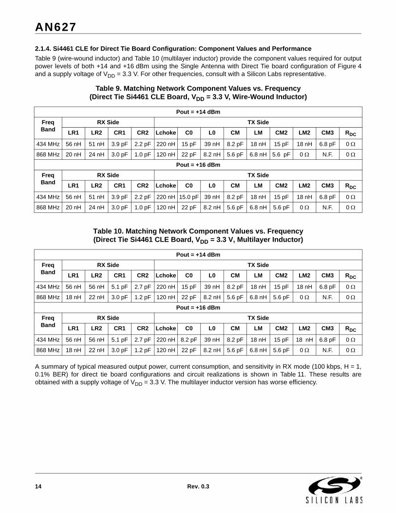
Figure 5. TX Matching Topology for Si4060/Si4460 Split TX/RX Board CLE Configuration
A summary of typical measured output power and current consumption for split board configurations with wire-wound inductors given in Table 13. These results are obtained with a supply voltage of VDD = 3.3 V.
Table 13. Output Power and Current Consumption vs. Frequency (Split Si4060/Si4460 CLE TX/RX Board, VDD = 3.3 V, Wire-Wound Inductors)
Pout = +10 dBm
Freq Band DDAC[6:0] WW Pout WW (dBm) IDC WW (mA)
434 MHz 19h 10.4 dBm 16.9 mA
868 MHz 19h 10.3 dBm 16.4 mA
Pout = +13–14 dBm
Freq Band DDAC[6:0] WW Pout WW (dBm) IDC WW (mA)
434 MHz 3Fh 13.4 dBm 22.7 mA
868 MHz 3Dh 14.3 dBm 24.8 mA

AN627
Rev. 0.3 19
2.2.2. Si4460 CLE for Direct Tie Board Configuration: Component Values and Performance
Table 14 provides the component values required for output power levels of both +10 and +12–13 dBm using theSingle Antenna with Direct Tie board configuration of Figure 6 and a supply voltage of VDD = 3.3 V. The matchingsof Table 14 are proper for wire-wound type of inductors. The same is given for multilayer inductors in Table 15. Forother frequencies, consult with a Silicon Labs representative. If the last inductor is only 0 , a proper bypass capcan be used instead (220 pF at 434M and 56 pF at 868/915M) if dc blocking is required. The L0 and C0 can bereplaced with negligible effect.
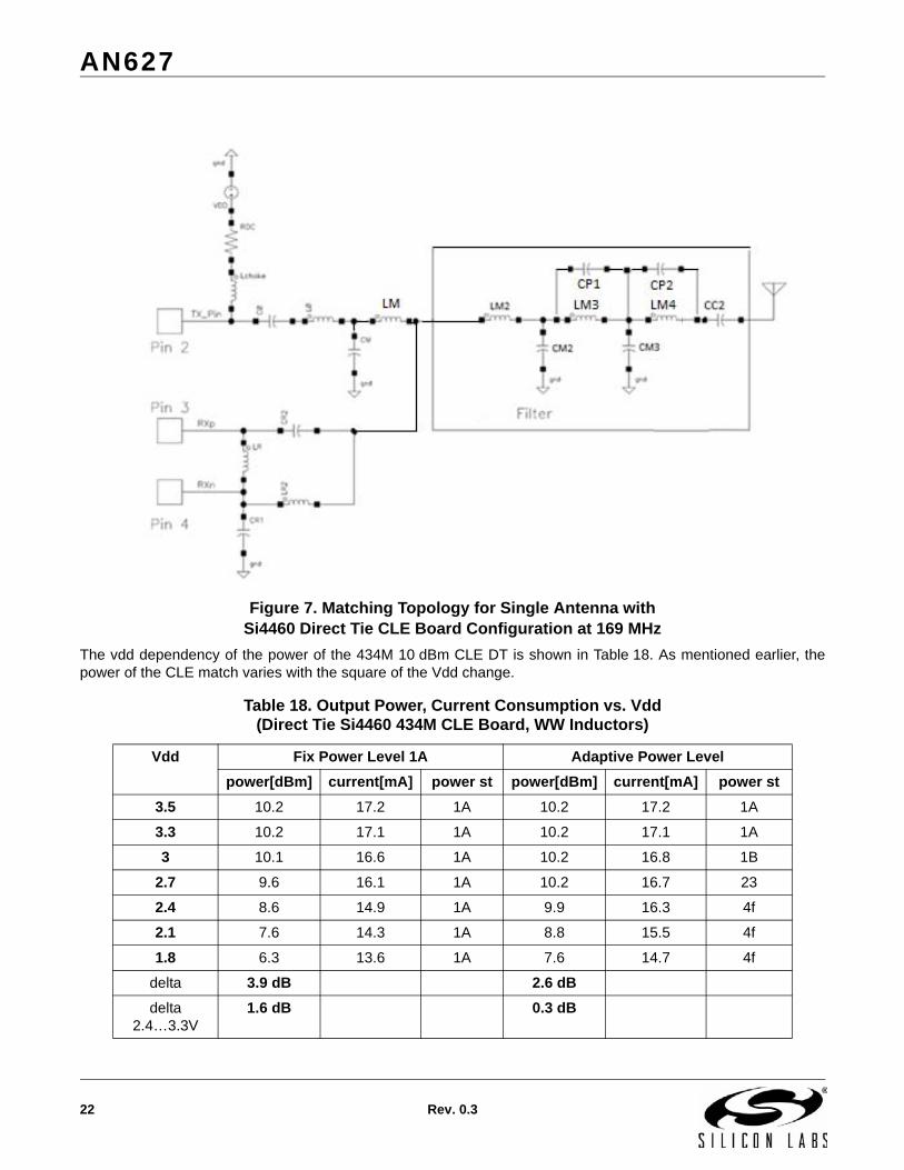
The 169 MHz Class E multilayer DT match has a significantly different structure as shown in Figure 7. The elementvalues are given in Table 16. The value of CC2 is 470 pF. Also, here, the 470 nH Lchoke inductor is a 0603 sizedone because this value does not exist in the 0402 size. Currently, the 169 MHz DT match exists with multilayerinductors only.
Table 14. Matching Network Component Values vs. Frequency (Direct Tie Si4460 CLE Board, VDD = 3.3 V, Wire-Wound Inductor)
Pout = +10 dBm
Freq Band RX Side TX Side
LR1 LR2 CR1 CR2 Lchoke C0 L0 CM LM CM2 LM2 CM3 RDC
434 MHz 56.0 nH 56.0 nH 5.1 pF 2.7 pF 220.0 nH 15.0 pF 56.0 nH 8.2 pF 18.0 nH 15.0 pF 18.0 nH 8.2 pF 0.0
868–915 MHz 18.0 nH 22.0 nH 3.0 pF 1.2 pF 120.0 nH 36.0 pF 6.8 nH 3.9 pF 6.8 nH 10.0 pF 6.8 nH 4.7 pF 0.0
Pout = +13 dBm
Freq Band RX Side TX Side
LR1 LR2 CR1 CR2 Lchoke C0 L0 CM LM CM2 LM2 CM3 RDC
HP 434 MHz 56.0 nH 56.0 nH 5.1 pF 2.7 pF 220.0 nH 10.0 pF 56.0 nH 10.0 pF 18.0 nH 15.0 pF 18.0 nH 8.2 pF 0.0
HP 868 MHz 20.0 nH 24.0 nH 3.0 pF 1.0 pF 120.0 nH 3.6 pF 19.0 nH 2.7 pF 9.1 nH 5.1 pF 9.1 nH 2.7 pF 0.0
Table 15. Matching Network Component Values vs. Frequency (Direct Tie Si4460 CLE Board, VDD = 3.3 V, Multilayer Inductor)
Pout = +10 dBm
Freq Band RX Side TX Side
LR1 LR2 CR1 CR2 Lchoke C0 L0 CM LM CM2 LM3 CM3 RDC
434 MHz 56.0 nH 56.0 nH 5.1 pF 2.7 pF 220.0 nH 18.0 pF 56.0 nH 8.2 pF 18.0 nH 15.0 pF 18.0 nH
8.2 pF 0.0
868-915 MHz 18.0 nH 22.0 nH 3.0 pF 1.2 pF 120.0 nH 36.0 pF 6.8 nH 3.3 pF 6.8 nH 10.0 pF 6.8 nH 4.7 pF 0.0
Pout = +13 dBm
Freq Band RX Side TX Side
LR1 LR2 CR1 CR2 Lchoke C0 LM1 CM1 LM2 CM2 LM3 CM3 RDC
HP 434 MHz 56.0 nH 56.0 nH 5.1 pF 2.7 pF 220.0 nH 6.2 pF 56.0 nH 10.0 pF 18.0 nH 15.0 pF 18.0 nH
8.2 pF 0.0
HP 868 MHz 18.0 nH 22.0 nH 3.0 pF 1.2 pF 120.0 nH 3.6 pF 18.0 nH 2.7 pF 9.1 nH 5.1 pF 9.1 nH 2.7 pF 0.0

AN627
20 Rev. 0.3
A summary of typical measured output power, current consumption and sensitivity in RX mode (100 kbps, H = 1,0.1% BER) for direct tie board configurations and circuit realizations is shown in Table 17. These results areobtained with a supply voltage of VDD = 3.3 V. The multilayer inductor versions usually has worse efficiency andsensitivity. The 13 dBm power range can be achieved at 868 and 915M with the dual band (868–915M) 10 dBmmatches as well. However, for that the maximum (0x4F) power state must be used. Also, with multilayer inductors,the dual band match cannot achieve the 13 dBm at 915M.
But, there is a possibility for tuning: by increasing the CM value (to 4.7p), the power at maximum power stateincreases, and even the multilayer 10 dBm match achieves 13.1 dBm (with 26.5 mA) at 915M. However, with4.7 pF CM, the efficiency becomes worse, and, thus, the 10 dBm power (10.2 dBm) is achieved only at power state0x22 with 20.6 mA.
The high power (HP) 868 match can achieve the 13 dBm with large margin (i.e. in a power state significantly lowerthan maximum) even with multilayer inductors. Unfortunately, at 434M, even the high power match cannot achievethe 13 dBm with multilayer inductors.
Table 16. Matching Network Component Values at 169 MHz (Direct Tie Si4460 CLE Board, VDD = 3.3 V, Multilayer Inductor)
Pout=+10 dBm
RX Side TX Side
LR1 LR2 CR1 CR2 Lchoke C0 L0 CM LM LM2 CM2 LM3 CM3 LM4 CP1 CP2 Lchoke RDC
220 nH 150 nH 12.0 pF 6.2 pF 470 nH 39 pF 22 nH 6.8 pF 56 nH 47 nH 18 pF 68 nH 18 pF 47 nH 3 pF 2 pF 470 nH 0
Table 17. Output Power, Current Consumption and RX Sensitivity vs. Frequency (Direct Tie Si4460 CLE Board, VDD = 3.3 V, Wire-Wound (WW) and Multilayer (ML) Inductors)
Pout = +10 dBm
Freq Band
DDAC[6:0] WW
Pout WW (dBm)
IDC WW (mA)
Sens WW (dBm)
DDAC[6:0] ML
Pout ML (dBm)
IDC ML (mA)
Sens ML (dBm)
169 MHz TBD TBD TBD TBD 23h 10.3 dBm 18.4 mA –102.8 dBm
434 MHz 1Ah 10.2 dBm 16.9 mA –106.1 dBm 2Ah 10.3 dBm 17.1 mA –103.1 dBm
868-915M,
868M op.
20h 10.5 dBm 19.7 mA –104.2 dBm 20h 10.7 dBm 19.7 mA –103.2 dBm
868-915M,
915M op.
20h 10.5 dBm 19.6 mA –104.1 dBm 20h 10.3 dBm 19.3 mA –102.9 dBm
AN627
Rev. 0.3 21
At all frequencies, the RX sensitivities achieved with the Direct Tie board configuration are within 2 dB of thoseobtained with the Split TX/RX board configuration.
Figure 6. Matching Topology for Single Antenna with Si4460 Direct Tie CLE Board Configuration
Pout = +12…13 dBm
HP 434 MHz
3Fh 13.3 dBm 23.0 mA –105.2 dBm 4Fh 12.3 dBm 23.3 mA –104.2 dBm
HP 868 MHz
44h 14.3 dBm 25.6 mA –104.2 dBm 3Ch 13.3 dBm 24.1 mA –102.0 dBm
868-915M,
868M op.
4Fh 13.7 dBm 25.5 mA –104.2 dBm 4Fh 13.4 dBm 24.7 mA –103.3 dBm
868-915M,
915M op.
4Fh 13.3 dBm 24.7 mA –104.1 dBm 4Fh 12.4 dBm 23.7 mA –103.3 dBm
Table 17. Output Power, Current Consumption and RX Sensitivity vs. Frequency (Direct Tie Si4460 CLE Board, VDD = 3.3 V, Wire-Wound (WW) and Multilayer (ML) Inductors)
AN627
22 Rev. 0.3
Figure 7. Matching Topology for Single Antenna with Si4460 Direct Tie CLE Board Configuration at 169 MHz
The vdd dependency of the power of the 434M 10 dBm CLE DT is shown in Table 18. As mentioned earlier, thepower of the CLE match varies with the square of the Vdd change.
Table 18. Output Power, Current Consumption vs. Vdd (Direct Tie Si4460 434M CLE Board, WW Inductors)
Vdd Fix Power Level 1A Adaptive Power Level
power[dBm] current[mA] power st power[dBm] current[mA] power st
3.5 10.2 17.2 1A 10.2 17.2 1A
3.3 10.2 17.1 1A 10.2 17.1 1A
3 10.1 16.6 1A 10.2 16.8 1B
2.7 9.6 16.1 1A 10.2 16.7 23
2.4 8.6 14.9 1A 9.9 16.3 4f
2.1 7.6 14.3 1A 8.8 15.5 4f
1.8 6.3 13.6 1A 7.6 14.7 4f
delta 3.9 dB 2.6 dB
delta 2.4…3.3V
1.6 dB 0.3 dB

AN627
Rev. 0.3 23
Since the match works in a strongly reduced power level setting (DDAC), there is room for compensation at lowVdds. During this compensation, the power setting can be increased to reduce the internal switching loss and thusmaintain the power as much as possible. For this, monitoring of the Vdd level is required. This so called “adaptivepower control” method gives significant improvement of the Vdd flatness, especially in the most critical 2.4–3.3 VVdd range. The result with the “adaptive power control” are also given in the table.
The flatness characteristics can be seen here to be typical for 10 dBm Si4060/4460 CLE and SQW matchesoperating on other bands as well.
At 13 dBm power levels, the Si4060/4460 CLE matches are working close to the maximum power state; so, theadaptive power control is not efficient there.
2.2.3. Si4060/4460 with Split TX\RX SWC Board Configuration: Component Values and Performance
The Si4460 SWC match were realized only in Direct Tie configuration. It will be detailed in section 2.2.4. If onewould like to make a split TX/RX configuration or TX only match for Si4060, please use the TX path of the DTsolution (Table 18). For the RX path, in split configuration, the Rx part of the CLE DT matches is recommended touse (LR1, LR2, CR1 and CR2 in Table 13 and 14) as the SWC DT matches may use other than 50 RX matchinput impedances.
The power and current consumption of the split solution in TX mode is very close to the DT results (Table 19).
Important to note that these SWC matches are designed for flat (dP<~1.2 dB in the 1.8…3.8 V Vdd range) powerand not for the highest efficiency. Due to this the impedance level of the match is lower and thus requires highercurrent for the same power.
2.2.4. Si4460 with Direct Tie TX/RX SWC Board Configuration: Component Values and Performance
Table 19 provides the component values required for output power levels of +10 dBm, using the Single Antennawith Direct Tie SWC board configuration of Figure 8 and a supply voltage of VDD = 3.3 V. The matches areworking with low cost multilayer inductors. For other frequencies pls. consult with a Silicon Labs representative.
The value of CC1 capacitor is equal to the value of C0 in Table 19.
A summary of typical measured output power, current consumption and sensitivity (100 kbps, H = 1, 0.1% BER) fordirect tie board configurations and circuit realizations is shown in Table 20. These results are obtained with asupply voltage of VDD = 3.3 V.
Table 19. Match Network Component Values vs. Frequency(Direct Tie Si4460 SWC Board, VDD = 3.3 V, Multilayer Inductors)
Pout = +10 dBm
Freq Band
RX Side TX Side
LR1 LR2 CR1 CR2 Lchoke C0 CM LM CM2 LM2 CM3 LM3 CM4
315 MHz 82 nH 68 nH 7.5 pF 3.6 pF 270 nH 470 pF 3.9 pF 27 nH 8.2 pF 22 nH 8.2 pF 0 N.F.
434 MHz 56 nH 56 nH 5.1 pF 2.7 pF 220 nH 270 pF 1.8 pF 22 nH 8.2 pF 18 nH 15.0 pF 18.0 nH 8.2 pF
868 MHz 18 nH 27 nH 3.0 pF 1.2 pF 120 nH 68 pF N.F. 8.2 nH 5.1 pF 6.2 nH 5.1 pF 0 N.F.
915 MHz 18 nH 22 nH 3.0 pF 1.0 pF 100 nH 56 pF N.F. 6.8 nH 3.9 pF 6.8 nH 3.9 pF 0 N.F.
AN627
24 Rev. 0.3
At all frequencies, the RX sensitivities achieved with the Direct Tie board configuration are within 1.5 dB of thoseobtained with the Split TX/RX board configuration.
The Vdd dependency of the flat SWC 4460 designs are given in Table 21. The flatness is 0.5…0.8 dB and 1–1.2 dB in the 2.1…3.3 V and 1.8…3.8 V Vdd range, respectively.
Table 20. Output Power, Current Consumption and Sensitivity vs. Frequency (Direct Tie Si4460 SWC Board, VDD = 3.3 V, Multilayer Inductors)
Pout = +10 dBm
Freq Band OB[5:0] DDAC[6:0] Pout (dBm) IDC (mA) Sens. (dBm)
315 MHz 0x21 0x44 10.28 dBm 23.50 mA –103.9 dBm
434 MHz 0x2B 0x44 10.40 dBm 26.60 mA –103.5 dBm
868 MHz 0x1E 0x44 10.50 dBm 23.70 mA –102.0 dBm
915 MHz 0x22 0x44 10.40 dBm 24.20 mA –102.7 dBm
Table 21. Output Power, Current Consumption vs. Vdd (Direct Tie Si4460 SWC Board, Multilayer Inductors)
Vdd [V] 315M 4460TSC10D315, PA_BIAS = 0x21,
PA_PWR_LVL = 0x44
434M 4460TSC10D434, PA_BIAS = 0x2B,
PA_PWR_LVL = 0x44
868M 4460TSC10D868, PA_BIAS = 0x1E,
PA_PWR_LVL = 0x44
915M 4460TSC10D915, PA_BIAS = 0x22,
PA_PWR_LVL = 0x44
Pout [dBm]
Idc [mA] Pout [dBm]
Idc [mA] Pout [dBm]
Idc [mA] Pout [dBm]
Idc [mA]
1,8 9.34 22.2 9.34 24.83 9.28 22.7 9.27 23.76
2.1 9.85 22.53 9.95 25.3 9.66 22.72 9.68 23.52
2.4 10.15 22.89 10.26 25.76 10.15 23.07 9.97 23.67
2.7 10.27 23.31 10.39 26 10.28 23.2 10.23 24.04
3 10.28 23.39 10.39 26.46 10.48 23.59 10.39 24.15
3.3 10.28 23.45 10.4 26.6 10.5 23.66 10.44 24.2
3.6 10.28 23.54 10.4 26.7 10.5 23.73 10.49 24.33
3.8 10.29 23.62 10.4 26.83 10.51 23.8 10.5 24.4
delta (2.1–3.3 V)
0.43 dB 0.92 0.45 dB 1.3 0.84 dB 0.94 0.76 dB 0.68
delta (1.8–3.8 V)
0.95 dB 1.42 1.06 dB 2 1.23 dB 1.1 1.23 dB 0.64

AN627
Rev. 0.3 25
Figure 8. Matching Topology for Single Antenna with Direct Tie SWC Board Configuration

AN627
26 Rev. 0.3
3. Switched Current (SWC) Matching Procedure Overview
3.1. SCW Matching Design for Split TX/RX BoardsIn this section, the procedure for matching the Si4461 RFIC on a Split TX/RX board with SWC matching type isdiscussed in detail. The Si4060/Si4460 SWC matching use the same procedure only the target external loadimpedance is different due to the lower power level and lower IC shunt output capacitance. The main steps in thematching procedure are summarized below:
1. Measure the typical PA shunt output capacitance (CPA) and resistance (RPA) of the chip.
2. Choose LCHOKE (pull-up inductor) for high impedance at the desired frequency of operation.
3. Select/calculate internal load resistance RLOAD_INT for the desired output power level.
4. Calculate PA bias current setting.
5. Calculate required external load impedance ZLOAD to present to the TX pin.
6. Construct a simple 2-element L-C matching network to transform the antenna load impedance (typically RANT = 50 ) to the calculated PA load impedance ZLOAD.
7. Add sections of lowpass filtering (while maintaining the desired impedance transformation ratio), necessary to attenuate the harmonic levels below the applicable regulatory standard.
3.1.1. Measurement of PA Shunt Output Capacitance/Resistance (CPA/RPA)
The output of the PA may be modeled as a shunt resistor RPA in parallel with a shunt capacitor CPA as illustrated inFigure 9. The values of RPA and CPA are not constant but instead vary over the frequency range of the Si4461 chip.It is necessary to determine the values of both RPA and CPA prior to constructing a matching network. The shuntoutput capacitance and resistance of the PA may be measured using a network analyzer.
Figure 9. Model of PA Output Circuit and Impedance Measurement Network

AN627
Rev. 0.3 27
DC bias to the PA output circuit is provided through a pull-up inductor, LCHOKE. The value of this pull-up inductorshould be chosen to present a very high impedance at the desired frequency of operation, such that it has no effectupon the impedance measurement. The inductance value should not be so large as to already be at (or past)parallel self-resonance at the desired operating frequency. The exact inductance value is not critical; however,Silicon Labs recommends the following range of inductance values (assuming 0402-size or 0603-size inductors) asa function of the desired operating frequency:
315 MHz: approximately 270 to 390 nH
470 MHz: approximately 220 nH
868 MHz: approximately 120 nH
915 MHz: approximately 100 nH
The network analyzer is connected to the TX output pin and pull-up inductor through a dc blocking capacitor toensure that the VDD supply voltage does not damage the port of the network analyzer. The Si4461 chip isconfigured for CW TX operation at a frequency close to (but not directly at) the desired frequency of operation. Thereason for this is that the chip is transmitting a signal (although at lower power) that is not correlated with the sweptsignal from the network analyzer. The network analyzer displays this anomalous signal as a “spike” in the S-parameter curve with the amplitude of the spike growing as the output power is increased. Thus, it is convenient tomove this spike slightly to one side of the frequency at which we desire to place the measurement marker. Also, itis advisable to configure the chip for a relatively low value of output power in order to prevent damage to the inputof the network analyzer. By trial-and-error, one can observe that the value of shunt output capacitance andresistance does not appear to be significantly influenced by the number of PA device fingers selected (i.e.,PA_DDAC property setting).
Figure 10. Si4461 PA Shunt Output Capacitance at 915M (TX Mode)

AN627
28 Rev. 0.3
The plot of Figure 10 illustrates the measured value of output admittance (with LCHOKE = 100 nH) at 915 MHz to beYOUT = GOUT + jBOUT = 1.25 + j14.26 ms. The output admittance may be measured at each desired frequency(with an appropriate selection of pull-up inductor LCHOKE) and is found to be the following:
169 MHz (LCHOKE = 470 nH): YOUT = GOUT + jBOUT = 0.010 + j1.79 ms
315 MHz (LCHOKE = 390 nH): YOUT = GOUT + jBOUT = 0.207 + j2.87 ms
470 MHz (LCHOKE = 220 nH): YOUT = GOUT + jBOUT = 0.291 + j4.96 ms
868 MHz (LCHOKE = 120 nH): YOUT = GOUT + jBOUT = 1.07 + j12.93 ms
915 MHz (LCHOKE = 100 nH): YOUT = GOUT + jBOUT = 1.25 + j14.26 ms
These admittance values are quite repeatable from chip to chip; so, these published values may be used by thedesigner without the need to remeasure each application.
However, it is apparent that this measured value of output admittance does not represent the equivalent internalshunt PA capacitance and resistance. This is due to the impedance-transforming effect of the series bond wire andtrace inductance as illustrated in Figure 9. As seen from outside the chip, the apparent value of shunt PAresistance will appear to be lower than the actual internal value. Additionally, the apparent value of shunt PAcapacitance will appear to be higher than the actual internal value.
The actual internal values may be calculated if the total value of series inductance (LSERIES = LBW + LTRACE) isknown. Although this value of inductance is not known precisely, it is reasonably estimated to be LSERIES = 2.9 nH(LBW = 1 nH, LTRACE = 1.9 nH). With a bit of mathematical manipulation, the formulas for the equivalent internal PAresistance and capacitance values may be derived as follows:
Equation 1.
Equation 2.
Equation 3.
Equation 4.
Equation 5.
Equation 6.
ZOUT ROUT jXOUT+1
YOUT-------------- 1
GOUT jBOUT+-------------------------------------- = = =
ROUT
GOUT
GOUT2
BOUT2
+------------------------------------------
=
XOUT
BOUT–
GOUT2
BOUT2
+------------------------------------------
=
ZOUT ROUT jXOUT+1
GPA jBPA+------------------------------ jXLSERIES
+= =
GPA jBPA+1
ROUT jXOUT jXLSERIES–+
------------------------------------------------------------------ =
GPA1
RPA-----------
ROUT
ROUT2
XOUT XLSERIES– 2+
-------------------------------------------------------------------------= =

AN627
Rev. 0.3 29
Equation 7.
From these equations, the following values of internal PA shunt resistance and capacitance are obtained:
169 MHz: RPA = 101 k, CPA = 1.68 pF
315 MHz: RPA = 4991 , CPA = 1.427 pF
470 MHz: RPA = 3735 , CPA = 1.611 pF
868 MHz: RPA = 1356 , CPA = 1.970 pF
915 MHz: RPA = 1226 , CPA = 2.006 pF
3.1.1.1. Impedance Values for Si4060/Si4460 SWC Configurations
As mentioned earlier, the SWC match design process flow is the same for the Si4060/Si4460, but the chip outputimpedance, power level, current magnitude (and thus the RLOAD_INT) are different. In this step, the measuredSi4060/Si4460 output admittances and internal RC equivalents are given:
The Si4060/Si4460 output admittance is measured at each desired frequency (with an appropriate selection of pull-up inductor LCHOKE) and is found to be as follows:
169 MHz (LCHOKE = 470 nH): YOUT = GOUT + jBOUT = 0.75 + j1.01 ms
315 MHz (LCHOKE = 390 nH): YOUT = GOUT + jBOUT = 0.18 + j1.74 ms
434 MHz (LCHOKE = 220 nH): YOUT = GOUT + jBOUT = 0.25 + j2.36 ms
470 MHz (LCHOKE = 220 nH): YOUT = GOUT + jBOUT = 0.25 + j2.88 ms
868 MHz (LCHOKE = 120 nH): YOUT = GOUT + jBOUT = 0.79 + j7.57 ms
915 MHz (LCHOKE = 100 nH): YOUT = GOUT + jBOUT = 0.84 + j7.85 ms
The Si4060/Si4460 internal PA shunt resistance and capacitance values are obtained via Equations 1 to 7:
169 MHz: RPA = 1330 , CPA = 0.95 pF
315 MHz: RPA = 5670 , CPA = 0.87 pF
434 MHz: RPA = 4100 , CPA = 0.85 pF
470 MHz: RPA = 4150 , CPA = 0.95 pF
868 MHz: RPA = 1590 , CPA = 1.24 pF
915 MHz: RPA = 1530 , CPA = 1.21 pF
BPA 2fCPA
XLSERIESXOUT–
ROUT2
XOUT XLSERIES– 2+
-------------------------------------------------------------------------= =

AN627
30 Rev. 0.3
3.1.2. Selection/Calculation of RLOAD_INT
Successfully obtaining the desired level of output power while minimizing current consumption or achieving Vddflatness depends strongly upon the load resistance presented to the PA. However, it is important to distinguishbetween the load impedance presented to the TX pin (RLOAD) and the impedance present at the drain of the outputdevices internal to the chip (RLOAD_INT). These values are different due to the impedance-transforming effect of theseries bond wire inductance and trace inductance (discussed in the previous section). It is apparent that, due to theseries inductance (LBW-LTRACE) and internal shunt PA capacitance (CPA), the effective internal load resistanceRLOAD_INT is larger than RLOAD. The total internal load resistance (RTOTAL) seen by the PA output device is theparallel combination of RPA and RLOAD_INT.
The power extracted from the PA output devices may be readily calculated as PPA = IPA2 x RTOTAL. Note that the
power sourced from the PA output devices (PPA) is not the same as the power delivered (POUT) to the loadimpedance, RLOAD, because some power is dissipated in the internal PA resistance, RPA. For a given value of PAoutput current IPA, the output power may be increased by presenting a larger total load impedance. Obviously, thisstatement only holds true for sufficiently small values of RTOTAL, such that clipping of the peaks of the drain voltagewaveform does not occur. That is to say, the voltage swing at the drain of the output device must be held to areasonably low value. A reasonable design constraint is to keep the peak drain voltage swing at VPK ≤ VDD – 0.7 V.This provides some voltage headroom on the output devices to ensure they remain in a linear region and continueto operate as switched current sources. It also allows for some tolerance against variations in supply voltage; if theoutput devices remain in a linear operating region, the output power is not significantly a function of supply voltage.The voltage peak at the internal drain node is not the same value as may be measured at the TX output pin of thedevice (again due to the impedance transforming effects of the series inductance).
It is also clear that, if the desired output power level is low enough, drain voltage clipping is not a concern. Thereare many combinations of IPA and RTOTAL that will theoretically provide the target value of PPA and thus also POUT.Optimal current efficiency is obtained by selecting the lowest possible value of IPA (i.e., highest value of RTOTAL)that will result in a drain voltage waveform that remains just below clipping amplitude at the operation supplyvoltage. However, if the design target is the flat power vs. Vdd characteristic, the load impedance has to bedecreased to avoid clipping even at the lowest possible supply level. In this case, the current efficiency will not beoptimal at higher Vdd levels because the target power is achieved with lower voltage swing (and higher currentmagnitude) optimized for the low Vdd level. In other words, efficiency has to be sacrificed to achieve flatness.
On the other side, If the design target is the highest efficiency at a given supply voltage, the value of RTOTALcannot be made arbitrarily large; it is self-evident that it cannot be larger than the internal equivalent parallelresistance of the PA itself (RPA). The limiting case would occur if the transformed value of load impedance(RLOAD_INT) was infinite, such that RTOTAL = RPA // RLOAD_INT ≈ RPA. In such a case, all of the output power wouldbe dissipated in the output devices themselves rather than being delivered to the load impedance. Thus, theincremental benefit to PA efficiency diminishes as RLOAD (and thus RLOAD_INT) is raised to higher and highervalues.
The output impedance measurements of the previous section indicate that the internal parallel output resistance ofthe PA output device is RPA = 1226 (using the Si4461 at 915 MHz as an example. For the Si4460/4060, the Rpais 1530 ). It is desirable to present an effective internal load impedance, RLOAD_INT, that is significantly lower thanthe PA output resistance itself so that most of the power is delivered to the load and not dissipated in the PA outputdevices. However, this constraint is weakly defined; so, there are many possible values of RLOAD_INT that could beconsidered as satisfactory. It is necessary to provide further design constraints or “rules of thumb” in order to selectan appropriate value of RLOAD_INT.
One factor to consider is the impedance transformation factor required from the external matching network. Theantenna load impedance (into which the output power must eventually be delivered) is typically a low value, suchas 50 . The external matching network must transform this antenna impedance (RANT) into the load impedance(RLOAD) seen at the TX pin, which is then further transformed by the series bond wire/trace inductance into theinternal load resistance (RLOAD_INT). The Q-factor of the external matching network is approximately proportionalto the square root of the ratio RLOAD:RANT, and thus, as RLOAD is made larger, the required Q-factor of the externalnetwork also increases. If the required impedance transformation ratio is too large, the loss of the externalmatching network may increase, and tuning of the circuit may become sensitive to component tolerances.
An additional factor to consider is the amount of power dissipated in the internal PA devices that is considered
AN627
Rev. 0.3 31
acceptable. This is a loss term that decreases current efficiency; so, it is desirable to make it as small as possible.As the internal PA resistance RPA is not infinite, this loss term cannot be made zero. However, it can be minimizedby making the value of RLOAD_INT small in comparison to RPA, such that most of the power is delivered to theoutput load and not dissipated in the PA devices.
Thus the selection criteria for RLOAD_INT may be summarized as follows:
A large value of RLOAD_INT increases RTOTAL, thereby improving the current efficiency (by requiring a lower value of IPA for a given target value of PPA).
A small value of RLOAD_INT decreases the percentage of power dissipated in the internal PA resistance.
A small value of RLOAD_INT decreases the impedance transformation ratio required from the external matching network, thus decreasing losses due to finite Q of discrete components and improving sensitivity to component tolerances.
A small value of RLOAD_INT ensures that the peak drain voltage does not exceed levels where clipping may occur. This is the most important condition for flat power vs. Vdd characteristic, even at the lowest Vdd limit.
Given these somewhat conflicting design goals, the selection of RLOAD_INT is made as a compromise to partiallysatisfy all four criteria and is stated as the following rule-of-thumb:
RLOAD_INT shall be chosen as large as possible while not exceeding RPA/5 or 5 x RANT, while remaining lowenough to ensure VPK < VDD – 0.7 V (with flat VDD design, the VPK can be fine-tuned during bench evaluation tosatisfy the specification).
In the Si4461 high-efficiency match design example at 915 MHz with RPA = 1226 , RANT = 50 , and a targetoutput power level of +14 dBm, this rule of thumb leads to choosing RLOAD_INT ≈ 90 (limited by the VPK designconstraint at 3.3 V Vdd, as will be shown shortly). A larger value of RLOAD_INT may be selected if the target outputpower level is reduced (e.g., RLOAD_INT ≈ 120 for POUT = +13 dBm). Similarly, for +10 dBm high-efficiencySi4060/Si4460 SWC solutions, RLOAD_INT ≈ 240 is the optimum. For flat power design, the optimum impedanceis around 50 for 13 dBm and 120–140 for 10 dBm.
3.1.3. Calculation of PA Bias Current IPA
The total load resistance is readily calculated as the parallel combination of RLOAD_INT and RPA. In our Si446114 dBm example:
Equation 8.
The finite value of RPA implies that some output power will be internally dissipated in the output device itself, andthus the power delivered to the load will be less than that obtained from straightforward calculations of P = I2 x R.This loss factor may be calculated as:
Equation 9.
This internal loss is unavoidable; it is simply necessary to adjust the PA bias current for a higher level in order tocompensate for this power loss.
If the external matching network is assumed to be lossless (i.e., discrete matching components with infinite Q), theonly loss in the circuit is due to PLOSS_INT. For a target output power POUT delivered to the load, the PA current maybe calculated as the following:
RTOTAL1
1RPA----------- 1
RLOAD_INT--------------------------- +
-------------------------------------------------------- 1
11226------------- 1
90------ +
------------------------------------- 83.84 = = =
PLOSS_INT 10 logRPA
RPA RLOAD_INT+-------------------------------------------- 10 log
12261226 90+-------------------------- 0.31 dB–= = =

AN627
32 Rev. 0.3
Equation 10.
If the desired output power level is chosen as POUT = +14 dBm = 25 mW, PPA = 14.0 +0.31 = 14.31 dBm = 27.0 mW and the PA current may be calculated as follows:
Equation 11.
Thus, IPA = 17.95 mA (RMS) or 25.38 mA peak current (50.76 mA pk-pk) at the fundamental frequency. Thiscurrent amplitude would theoretically result in peak internal drain voltage swing of VPEAK = IPA_PEAK xRTOTAL = 25.38 mA x 83.84 = 2.13 Vpk. This peak drain voltage swing appears acceptably small to ensurelinearity (non-clipping), assuming a supply voltage of VDD ≥ VPEAK + 0.7 V = 2.83 V. However, this voltagecalculation takes into account only the peak voltage at the fundamental frequency. The square-wave current pulsedelivered by the switched output devices is presented with a considerably different load impedance at harmonicfrequencies; the resulting harmonic voltage components may add to the fundamental to result in a somewhat largerpeak drain voltage than that calculated above. Therefore, it may be prudent to allow for a slightly greater voltageheadroom, if flatness of power vs. VDD is a design goal.
As the output power is theoretically a function of only IPA and RLOAD_INT, the output power should not vary withchanges in supply voltage as long as IPA remains at its programmed value. If greater tolerance against a reductionin supply voltage is desired, it would be necessary to select a lower target value for RLOAD_INT; this would result ina lower peak voltage swing (at the expense of an increase in the required value of IPA and thus overall currentconsumption of the chip).
The PA output devices operate as programmable switched current sources and, ideally, deliver square wavepulses of current to the load. The amplitude of these square wave current pulses is programmable through theproperties PA_PWR_LVL at 0x2201 and PA_BIAS_CLKDUTY at 0x2202. The value of PA bias current pertransistor unit finger (in increments of 10 µA) is configured by the OB[5:0] field in the PA_BIAS_CLKDUTYproperty, while the total number of enabled transistor fingers is configured by the DDAC[6:0] field in thePA_PWR_LVL property. The total amplitude of the square wave current pulse is the product of these two values.As an example, if the OB[5:0] field is set to 0x22 = 34d and the DDAC[6:0] field is set to 0x64 = 100d, theprogrammed amplitude of the current pulse is IBIAS = 34.0 mA (34 x 10 µA per finger x 100 fingers). Since theamplitude of the current pulse is a product of two values, it is often possible to obtain the same bias currentamplitude with different combinations of settings. Silicon Labs recommends using a nominal value ofDDAC[6:0] = 0x64 = 100 fingers and then selecting OB[5:0] as required; this allows for both upwards anddownwards adjustment range if fine tuning of the output power is required.
The previously-calculated value for IPA_PK of 25.38 mA represented the required current amplitude at thefundamental frequency. This is not the same as the amplitude of the square wave current pulse configured throughthe OB[5:0] and DDAC[6:0] fields. The relationship between the amplitude of a 50% duty cycle square wave pulsetrain and the amplitude of its fundamental component may be found through Fourier analysis to be:
Equation 12.
This value of bias current could be obtained by setting OB[5:0] = 0x28 = 400 µA per finger andDDAC[6:0] = 0x64 = 100 fingers, for a total square wave current pulse amplitude of 40.0 mA. The average (dccomponent) of this 50% duty cycle current pulse is half of the amplitude: IBIASDC = IBIAS/2 = 19.95 mA.
IPA
PPA
RTOTAL---------------------
POUT PLOSS–
RTOTAL--------------------------------------= =
IPA0.027083.84
------------------ 17.95 mA= =
IBIAS 2 IPA_PK4--- 2 25.38 mA
4--- 39.9 mA= = =

AN627
Rev. 0.3 33
This analysis assumes a square waveform with 50% duty cycle. The duty cycle of the current pulse may beadjusted to other selected values through the CLK_DUTY[1:0] field in the PA_BIAS_CLKDUTY property. Theanalysis for other values of duty cycle is not discussed here.
3.1.4. Calculation of Required ZLOAD at the TX Pin
It is desired that the PA output devices be presented with a purely-real load at the fundamental frequency (i.e.,ZTOTAL = RTOTAL + j0). It is thus necessary to present a load impedance ZLOAD at the TX pin that appearsinductive, such that the inductive reactance cancels the internal shunt capacitance of the PA devices (CPA). It isnecessary to calculate the external load impedance that when placed in series with LSERIES = LBW +LTRACE ≈ 2.9 nH and then in shunt with CPA = 2.006 pF results in ZLOAD_INT = 90 +j0 = RLOAD_INT (continuingour Si4461 design example at 915 MHz).
The required impedance value ZLOAD to present to the TX pin may easily be determined through graphical means(e.g., Smith Chart) or through the use of the impedance transformation equation shown below.
Equation 13.
For our 14 dBm design example at 915 MHz, this may be calculated to be ZLOAD = 43.3 + j28.3 .
3.1.5. Transforming RANT into ZLOAD
A simple two-element L-C match is thus required to transform the (assumed) 50 antenna impedance to thecalculated value of ZLOAD = 43.3 + j28.3 . The required component values are again found easily through use ofa Smith Chart and are determined to be a shunt capacitor CM1 = 1.37 pF and series inductor LM1 = 7.9 nH.Standard 5% component tolerance values of CM1 = 1.2 pF and LM1 = 8.2 nH are considered sufficiently close, asshown in Figure 11.
If lower impedance required (for a flat Vdd characteristic) the LM1 can be reduced. To keep the ZLOAD_INT purereal at the internal TX pin slight increase of the CM1 is required: E.g. with LM1 = 5.6 nH and CM1 = 1.5 pF theresulted a ZLOAD_INT = ~64 instead of the original ~90 .
Figure 11. Simplified SwCurr Match for +14 dBm at 915 MHz
ZLOAD ZR jZI+GLOAD_INT
GLOAD_INT2
BCPA2
+-----------------------------------------------------
= = j XLseries
BCPA
GLOAD_INT2
BCPA2
+-----------------------------------------------------–
–

AN627
34 Rev. 0.3
3.1.6. Verifying Initial TX Performance
The next step is to verify the performance of this simple SwCurr match. The match of Figure 11 was constructed onan RF test card and characterized. The measured performance for OB[5:0] = 0x28 (400 µA per finger), andDDAC[6:0] = 0x64 (100 fingers) was:
The measured output power of +13.27 dBm for VDD = 3.3 VDC was about 0.73 dB below the target output powerof +14.0 dBm. After some bench investigation, the following reasons were discovered for the discrepancy:
The PA output resistance (RPA) in large-signal conditions is somewhat lower than the small-signal value measured in "3.1.1. Measurement of PA Shunt Output Capacitance/Resistance (CPA/RPA)" on page 26. This results in a greater value of PLOSS and thus a lower output power.
The measured PA bias current (through LCHOKE) was slightly lower than the programmed value, due to some compression in large-signal conditions. This also resulted in lower-than-calculated output power.
The value of PA bias current was increased to OB[5:0] = 0x2D (450 µA per finger) to compensate for the additionalloss.
There is some reduction in output power as the VDD supply voltage is reduced; this is in agreement with ourexpectation of voltage clipping at supply voltages less than VDD ≈ 2.8 to 3.0 V. As stated in "2. Summary ofMatching Network Component Values" on page 6, the Si4461 SWC 13 dBm 868M board designed for flat Vddcharacteristic has only 1.5dB drop in the 1.8–3.8 V supply voltage range. This is due to the fact that the impedance(ZLOAD_INT) is lower (~60 ).
The measured conducted harmonics for the 915M simplified SwCurr match example are shown in Figure 12.
LM1 CM1 DDAC OB VDD POUT IDD
8.2 nH 1.2 pF 0x64 0x28 1.80 VDC 11.02 dBm 28.93 mA2.10 VDC 11.72 dBm 30.51 mA2.40 VDC 12.08 dBm 31.71 mA2.70 VDC 12.23 dBm 32.62 mA3.00 VDC 13.02 dBm 33.48 mA3.30 VDC 13.27 dBm 33.65 mA3.60 VDC 13.44 dBm 33.81 mA
2-Element Match
LM1 CM1 DDAC OB VDD POUT IDD
8.2 nH 1.2 pF 0x64 0x2D 1.80 VDC 11.22 dBm 29.78 mA2.10 VDC 12.14 dBm 32.00 mA2.40 VDC 12.71 dBm 33.57 mA2.70 VDC 12.93 dBm 34.59 mA3.00 VDC 13.71 dBm 35.45 mA3.30 VDC 14.05 dBm 35.67 mA3.60 VDC 14.26 dBm 35.85 mA
2-Element Match

AN627
Rev. 0.3 35
Figure 12. Conducted Harmonics for SwCurr Match at 915 MHz (N = 2)
AN627
36 Rev. 0.3
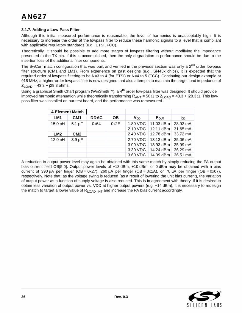
3.1.7. Adding a Low-Pass Filter
Although this initial measured performance is reasonable, the level of harmonics is unacceptably high. It isnecessary to increase the order of the lowpass filter to reduce these harmonic signals to a level that is compliantwith applicable regulatory standards (e.g., ETSI, FCC).
Theoretically, it should be possible to add more stages of lowpass filtering without modifying the impedancepresented to the TX pin. If this is accomplished, then the only degradation in performance should be due to theinsertion loss of the additional filter components.
The SwCurr match configuration that was built and verified in the previous section was only a 2nd order lowpassfilter structure (CM1 and LM1). From experience on past designs (e.g., Si443x chips), it is expected that therequired order of lowpass filtering to be N=3 to 4 (for ETSI) or N=4 to 5 (FCC). Continuing our design example at915 MHz, a higher-order lowpass filter is now designed that also attempts to maintain the target load impedance ofZLOAD = 43.3 + j28.3 ohms.
Using a graphical Smith Chart program (WinSmith™), a 4th order low-pass filter was designed. It should provide improved harmonic attenuation while theoretically transforming RANT = 50 to ZLOAD = 43.3 + j28.3 . This low-pass filter was installed on our test board, and the performance was remeasured.
A reduction in output power level may again be obtained with this same match by simply reducing the PA outputbias current field OB[5:0]. Output power levels of +13 dBm, +10 dBm, or 0 dBm may be obtained with a biascurrent of 390 µA per finger (OB = 0x27), 260 µA per finger (OB = 0x1A), or 70 µA per finger (OB = 0x07),respectively. Note that, as the voltage swing is reduced (as a result of lowering the unit bias current), the variationof output power as a function of supply voltage is also reduced. This is in agreement with theory. If it is desired toobtain less variation of output power vs. VDD at higher output powers (e.g. +14 dBm), it is necessary to redesignthe match to target a lower value of RLOAD_INT and increase the PA bias current accordingly.
LM1 CM1 DDAC OB VDD POUT IDD
15.0 nH 5.1 pF 0x64 0x2E 1.80 VDC 11.03 dBm 28.92 mA2.10 VDC 12.11 dBm 31.65 mA
LM2 CM2 2.40 VDC 12.78 dBm 33.72 mA12.0 nH 3.9 pF 2.70 VDC 13.13 dBm 35.06 mA
3.00 VDC 13.93 dBm 35.99 mA3.30 VDC 14.24 dBm 36.29 mA3.60 VDC 14.39 dBm 36.51 mA
4-Element Match

AN627
Rev. 0.3 37
In practice, the value of PA output bias current is selected to nominally center the desired output power level.Further fine adjustment of the output power (upwards or downwards) may be accomplished by selecting a larger orsmaller number of output device fingers (DDAC[6:0] field). The default value of DDAC used in the abovemeasurements is 100 fingers (0x64). As the allowed range for this field is from 0 to 127 fingers, there remains roomfor upwards or downwards adjustment of the output power.
LM1 CM1 DDAC OB VDD POUT IDD
15.0 nH 5.1 pF 0x64 0x27 1.80 VDC 10.79 dBm 28.08 mA2.10 VDC 11.60 dBm 30.02 mA
LM2 CM2 2.40 VDC 12.05 dBm 31.48 mA12.0 nH 3.9 pF 2.70 VDC 12.24 dBm 32.44 mA
3.00 VDC 12.98 dBm 33.30 mA3.30 VDC 13.16 dBm 33.47 mA3.60 VDC 13.25 dBm 33.64 mA
0x64 0x1A 1.80 VDC 9.34 dBm 24.50 mA2.10 VDC 9.59 dBm 25.22 mA2.40 VDC 9.69 dBm 26.08 mA2.70 VDC 9.75 dBm 26.86 mA3.00 VDC 10.14 dBm 27.59 mA3.30 VDC 10.20 dBm 27.70 mA3.60 VDC 10.25 dBm 27.82 mA
0x64 0x07 1.80 VDC 0.27 dBm 15.12 mA2.10 VDC 0.13 dBm 15.80 mA2.40 VDC 0.10 dBm 16.68 mA2.70 VDC 0.08 dBm 17.46 mA3.00 VDC 0.27 dBm 18.12 mA3.30 VDC 0.31 dBm 18.22 mA3.60 VDC 0.34 dBm 18.33 mA
4-Element Match

AN627
38 Rev. 0.3
The measured conducted harmonics for VDD = 3.3 V, OB = 0x2E (460 µA per finger), and DDAC = 0x64 (100fingers) for the schematic of Figure 14 are shown in Figure 13 below. These conducted levels of harmonics nowcomply with the Radiated Spurious Emission requirements of FCC Part 15.205/209.
Figure 13. Conducted Harmonics for SwCurr Match at 915 MHz (N = 4)

AN627
Rev. 0.3 39
3.1.8. Final Split TX/RX Schematic
The final schematic for a Split Si4461 TX/RX board Switched Current Match at 915 MHz for +14 dBm output poweris shown in Figure 14 below.
Figure 14. Final Schematic for Split SwCurr Match for +14 dBm at 915 MHz
3.1.9. Improved Efficiency at Lower Output Power Levels
As discussed in "3.1.2. Selection/Calculation of RLOAD_INT" on page 30, the selection of RLOAD_INT is drivenlargely by the desired target output power level and the available VDD supply voltage. It is necessary to select avalue of RLOAD_INT such that drain voltage compression/clipping does not occur for the commanded output powerlevel. If a lower output power level is desired, the value of RLOAD_INT may be increased, thus requiring a lowervalue of PA bias current but providing improved current efficiency.
The design calculations and resulting component values shown in the previous sections assumed a target outputpower level of +14 dBm. If the desired output power level is reduced to (e.g.) +13 dBm, a higher value ofRLOAD_INT ≈ 120 may be selected. In such a case, the design equations will result in the following parametersand component values:
RTOTAL = 109.3
PLOSS_INT = –0.41 dB
IPA = 14.2 mA (RMS fundamental), 20.0 mA (peak fundamental)
IBIAS = 31.4 mA → OB[5:0] = 0x20
ZLOAD = 41.15 + j40.29
CM1 = 1.8 pF, LM1 = 11 nH
For the reasons discussed earlier, the initial measured output power for this design was again about 0.6 dB belowthe target output power of +13.0 dBm. The value of PA bias current was increased to OB[5:0] = 0x22 (340 µA perfinger) to compensate for the additional loss, and the performance was remeasured.
LM1 CM1 DDAC OB VDD POUT IDD
11.0 nH 1.8 pF 0x64 0x22 1.80 VDC 10.46 dBm 25.91 mA2.10 VDC 11.08 dBm 27.15 mA2.40 VDC 11.46 dBm 28.29 mA2.70 VDC 12.03 dBm 29.50 mA3.00 VDC 12.51 dBm 29.99 mA3.30 VDC 12.85 dBm 30.15 mA3.60 VDC 13.05 dBm 30.30 mA
2-Element Match

AN627
40 Rev. 0.3
A significant improvement in current efficiency may be observed. For Si4460/4060 10 dBm SWC designs, theimpedance should be even higher (~240 for high efficiency target or lower if flatness is a concern).
3.2. Overview of Matching Procedure for SWC Direct Tie BoardIn this section, the procedure for matching the Si4461 RFIC on an SWC Direct Tie (DT) board is discussed indetail. The procedure for the Si4460 chip is the same with different impedance and thus element values. The mainsteps in the matching procedure are summarized below:
1. Measure the typical PA shunt output capacitance (CPA) and resistance (RPA) of the chip.
2. Choose LCHOKE (pull-up inductor) for high impedance at the desired frequency of operation.
3. Select/calculate internal load resistance RLOAD_INT for the desired output power level.
4. Calculate PA bias current setting.
5. Calculate required external load impedance ZLOAD to present to the TX pin.
6. Construct a simple 2-element L-C matching network to transform the antenna load impedance (typically RANT = 50 ) to the calculated PA load impedance ZLOAD.
7. Add sections of low-pass filtering (while maintaining the desired impedance transformation ratio) necessary to attenuate the harmonic levels below the applicable regulatory standard.
8. Calculate the impedance at the common Direct Tie point in the TX=OFF state (i.e., RX mode).
9. Construct a standard four-element RX balun/matching network, assuming this value of impedance as the source impedance for the match.
10. Tie the TX and RX paths together at the common-impedance point, and verify that the performance of each path has not been significantly degraded.
A comparison of the above procedure with that shown in "3.1. SCW Matching Design for Split TX/RX Boards" onpage 26 reveals that the first seven steps are identical. For either type of board configuration (Split TX/RX or DirectTie), it is necessary to first construct a TX match. In the case of a DT board configuration, the RX match is addedafter the TX match has been designed.

AN627
Rev. 0.3 41
3.2.1. Concept of Direct Tie Matching
In the Direct Tie board configuration, the TX and RX paths are tied directly together at a common point without theuse of an RF switch. Careful design procedure must be followed to ensure that the RX input circuitry does not loaddown the TX output path while in TX mode and that the TX output circuitry does not degrade receive performancewhile in RX mode.
The RX input circuitry of the Si4461 and Si4460 chip contains a set of switches that aids in isolation of the TX andRX functions. This set of switches is implemented internally as shown in Figure 15.
Figure 15. RX Input Switches for Direct Tie Operation
These three switches are activated and closed simultaneously upon entering TX mode; the switches remain openin all other modes, including RX mode. Closing these switches during TX mode effectively shorts the RXp and RXninput pins together and also shorts them to GND. The effective circuit may be redrawn as shown in Figure 16.Inductor LR2 and capacitor CR2 have effectively been placed in parallel by the closure of the switches and areconnected to GND. If the values of these components are chosen for resonance at the desired operatingfrequency, a very high impedance is presented to the TX path resulting in very little degradation in TX outputpower. Also, by shorting the input pins of the LNA together and simultaneously to GND, the LNA is protected fromthe large signal swing of the TX signal. This feature allows connection of the TX path to the RX path withoutdamage to the LNA.

AN627
42 Rev. 0.3
Figure 16. Effective Direct Tie Circuit in TX Mode
In RX mode, the output transistors of the PA are in the OFF state. However, the output impedance parameters ofthe PA (RPA and CPA) do not vary greatly between TX and RX modes. (The shunt output capacitance doesdecrease slightly in RX mode as compared to TX mode, but the decrease is only about 10%.) As a result, theoutput impedance parameters determined in "3.1.1. Measurement of PA Shunt Output Capacitance/Resistance(CPA/RPA)" on page 26 may be reasonably used in both TX and RX modes. The impedance of the pull-upinductor, LCHOKE, is quite high and the impedance of the coupling cap, C0, is quite low, and both may be ignoredfor this discussion.
A key step in the DT matching procedure is to design/measure the impedance at the common direct tie point and tothen construct the four-element RX match, assuming that impedance value as the source impedance. Thiscommon-point impedance is typically not exactly 50 ; however, there is nothing that prevents construction of anRX matching network for an arbitrary value of source impedance.
As discussed in "3.1.5. Transforming RANT into ZLOAD" on page 33, the impedance seen looking back into thematch/low-pass filter network (i.e., looking back into LM1 with the chip disconnected) is equal to ZLOAD.Additionally, connecting the TX pin of the chip results in placing the LSER-RPA-CPA network in shunt to GND at thispoint, as shown in Figure 17. This modifies the source impedance presented to the input of the RX matchingnetwork away from the ZLOAD value. While it is possible to express the resulting impedance mathematically interms of ZLOAD and the PA output impedance parameters, the resulting equation is rather unwieldy; it is muchsimpler to graphically determine the impedance on a Smith Chart.
The resulting impedance is reasonably close to being purely real and is close to (but slightly lower than) RLOAD_INT.This is not unexpected; if the series bond wire/trace inductance (LSERIES) was equal to zero, the resultingimpedance would be exactly equal to RLOAD_INT. A non-zero value of LSERIES has an impedance-transformingeffect that tends to lower the impedance observed at this point.

AN627
Rev. 0.3 43
Figure 17. Effective Direct Tie Circuit in RX Mode
This (nearly) purely-real common impedance value now allows for a convenient tie-point that simultaneouslysatisfies the matching requirements for both signal paths. In TX mode, the RX matching network presents a highimpedance and thus does not load down the TX signal. In RX mode, the RPA-CPA-LSERIES network placed inparallel with ZLOAD results in an approximately-real impedance that may be used as the source impedance forconstruction of the RX match. In this fashion, the performance of both signal paths may be maintained near theiroptimum levels (i.e., performance levels similar to those obtainable with a Split TX/RX board configuration).
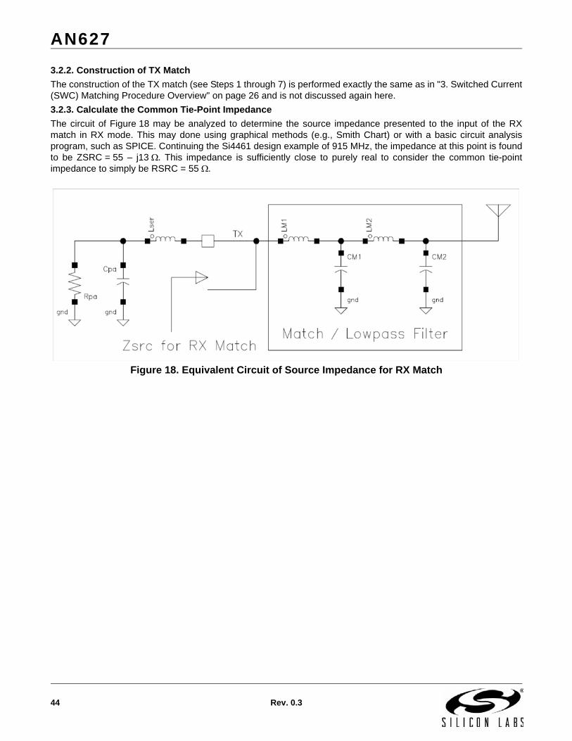
AN627
44 Rev. 0.3
3.2.2. Construction of TX Match
The construction of the TX match (see Steps 1 through 7) is performed exactly the same as in "3. Switched Current(SWC) Matching Procedure Overview" on page 26 and is not discussed again here.
3.2.3. Calculate the Common Tie-Point Impedance
The circuit of Figure 18 may be analyzed to determine the source impedance presented to the input of the RXmatch in RX mode. This may done using graphical methods (e.g., Smith Chart) or with a basic circuit analysisprogram, such as SPICE. Continuing the Si4461 design example of 915 MHz, the impedance at this point is foundto be ZSRC = 55 – j13 . This impedance is sufficiently close to purely real to consider the common tie-pointimpedance to simply be RSRC = 55 .
Figure 18. Equivalent Circuit of Source Impedance for RX Match

AN627
Rev. 0.3 45
3.2.4. Construction of RX Match
It is next necessary to construct a four-element RX matching network to simultaneously provide an impedancematch as well as a single-ended-to-differential conversion function (i.e., balun). The mathematical derivation for therequired component values has been thoroughly described in “AN643 Si446x RX LNA Matching”; the relevantequations from that document are shown here.
Equation 14. .
Equation 15. .
Equation 16. .
Equation 17. .
Equation 18. .
Equation 19. .
In order to make use of the above equations, it is first necessary to know the LNA differential input impedance atthe desired frequency of interest. This has been measured by Silicon Labs and is shown in Figure 19. The value ofthe RX input impedance is the same for both the Si4461 and Si4460. At 915 MHz, the input impedance isZRX_LNA = 48.8 – j109.4 ; the equivalent parallel input resistance and capacitance may be calculated to beRLNA = 296 and CLNA = 1.33 pF.
LLNA1
RF2CLNA
----------------------------=
LR2
Re ZANT RLNA
RF----------------------------------------------=
LM
2LR2
2 Im ZANT RFLR2
----------------------------------- 1+
---------------------------------------------------=
LR1
LLNALM
LLNA LM+---------------------------=
CR11
RFLR2---------------------=
CR2 2CR1=

AN627
46 Rev. 0.3
Figure 19. Si4461/Si4460 RX Differential LNA Input Impedance
The source impedance to which the RX input must be matched is the common tie-point impedance of ZSRC = 55 (in the 915 MHz Si4461 design example). Plugging the values of ZANT, RLNA, and CLNA into the above equations,the following calculated RX match component values are obtained:
LR1 = 15.04 nH
LR2 = 22.19 nH
CR1 = 1.36 pF
CR2 = 2.72 pF
These exact values may be rounded to the nearest-available 5% component tolerance values to arrive atLR1 = 15 nH, LR2 = 22 nH, CR1 = 1.3 pF, and CR2 = 2.7 pF. If desired, as an additional step of confirmation, thismatch may be constructed in a “stand-alone” configuration (i.e., not connected to the TX path) and its impedancemeasured. It was found that the input impedance and resonance were slightly off-target, likely due to parasitic traceand pad effects. The component values were adjusted slightly to optimize the impedance at the desired frequency.
LR1 = 18 nH
LR2 = 22 nH
CR1 = 1.0 pF
CR2 = 3.0 pF

AN627
Rev. 0.3 47
The measured input impedance in RX mode for these component values is shown in Figure 20. The inputimpedance at the desired frequency of 915 MHz is 44 ; this is sufficiently close to the design target of 55 .
Figure 20. Si4461 SWC RX Match Input Impedance (RX and TX Modes)
It is also useful to verify the input impedance of this network in TX mode, when the LNA input pins are shortedtogether and also to GND. The input impedance of the match in TX mode is also shown in Figure 20 (magentatrace). It is seen that the circuit is nicely tuned to parallel-resonate at 915 MHz, thus presenting a very highimpedance (~1.4 k). This should allow the RX path to be connected to the TX path with very little degradation inTX mode.

AN627
48 Rev. 0.3
3.2.5. Direct Tie Connection of TX and RX Paths
The next step is to actually connect the TX and RX paths at the common tie point (just after the series dc blockingcapacitor). The TX and RX performance in the Direct Tie configuration is then remeasured.
The TX performance in Direct Tie configuration was measured as shown below.
Comparing with the previously-measured performance in Split configuration, the loss of output power is only~0.2 dB! This is considered quite acceptable DT performance.
The RX sensitivity is also measured. The typical RX sensitivity performance in a Split configuration is known (frommeasurements on a large number of other boards) for 2GFSK DR = 40 kbps Dev = 20 kHz (h = 1) condition to beapproximately –109.6 dBm for BER = 1E-3 (0.1%). The measured performance on this board in Direct Tieconfiguration is found to degrade by less than 1 dB. Again, this is considered quite acceptable performance.
LM1 CM1 DDAC OB VDD POUT IDD
8.2 nH 1.5 pF 0x64 0x2E 1.80 VDC 11.24 dBm 29.74 mA2.10 VDC 12.15 dBm 31.89 mA2.40 VDC 12.65 dBm 33.48 mA2.70 VDC 12.83 dBm 34.38 mA3.00 VDC 13.57 dBm 35.31 mA3.30 VDC 13.83 dBm 35.52 mA3.60 VDC 13.97 dBm 35.69 mA
2-Element TX Match
LR1 CR1 LR2 CR218.0 nH 3.0 pF 22.0 nH 1.0 pF Split = -109.6 dBm
DT = -108.8 dBm
4-Element RX Match RX Sens (DR=40K Dev=20K)

AN627
Rev. 0.3 49
3.2.6. Final Direct Tie Schematic
It is again necessary to add further stages of lowpass filtering in order to comply with the harmonic radiatedspurious emission requirements of various regulatory standards, such as FCC or ETSI. The resulting finalschematic for a Direct Tie board Si4461 Switched Current Match at 915 MHz for +14 dBm output power is shown inFigure 21.
Figure 21. Final Schematic for Direct Tie Si4461 SwCurr Match for +14 dBm at 915 MHz
AN627
50 Rev. 0.3
4. Class E (CLE) Matching Procedure Overview
Published matching procedures for well-defined classes of operation of switching amplifiers (such as Class-D orClass-E) may lead to operating conditions that exceed the maximum ratings (voltage or current) for thesemiconductor process. As a result, we turn to a “customized” matching methodology that satisfies our desire foroutput power and efficiency while maintaining operation below the maximum voltage and current ratings for theRFIC. Note that this matching methodology is based upon Class-E theory but adds additional steps to aid inconstraining the peak drain voltage. The drain voltage peak limit for long term reliable PA operation is 8 V in thecase of the EZRadioPRO® family.
4.1. Brief Overview of CLE Matching ProcedureThis application note discusses the CLE matching philosophy and procedure for the Si4060/Si4460/61 RFIC ingreat detail. However, some users may be interested in quickly gaining a high-level overview of the procedurebefore getting into the fine details. For those readers, the main points of the matching procedure are summarizedbelow:
Choose LCHOKE (pull-up inductor) for high impedance at the operating frequency, Fo.
Calculate the required value of ZLOAD at the given Fo.
Calculate the required PA switcher loss for a given VDD and desired output power. In the matchings applied here, instead of an external RDC, the necessary loss is introduced by tuning the PA switcher FET loss (i.e with the PA power level setting).
Choose a value for C0 (series capacitor).
Calculate L0 (series inductor) and the required matching component values LX and CX.
Design a Chebyshev LPF (for attenuation of harmonics).

AN627
Rev. 0.3 51
4.2. Power Amplifier Circuit DescriptionRF design engineers are familiar with matching conventional (Class A/B/C) power amplifiers. In such cases, thematching procedure is relatively simple: provide a load impedance that is the complex conjugate of the outputimpedance of the PA. The reader may also employ Load Pull techniques in which a match is found that optimizesthe output power but differs from the complex conjugate of the PA output impedance. In these conventional classesof power amplifiers, the output waveform ranges from a full 360 degree copy or reproduction of the drivingwaveform (e.g., Class A) to a partial (less than 360 degree) reproduction of the driving waveform (e.g., Class B orClass C).
However, the Class E type PA circuitry in the Pro family RFIC differs considerably from such a conventional poweramplifier. Specifically, the PA circuitry in the Pro family is capable of working as a “switching power amplifier” or“switching power converter”. The matching procedure for such a class of PA is entirely different and may not beimmediately intuitive.
4.3. Basic Switching PA Circuit TopologyAt the very heart of a switching PA is a switch. In the Si4060/Si4460/61, the switch is provided by group of NMOStransistors. Above the switcher FETs, a cascode stage with open collector output is used to increase the Vpeakallowed at the output. The number of bottom transistors can be tuned and sized to handle the current required forthe specified output power.
The higher-power Si4461 PA has 127 MOS switching fingers; so, the DDAC[6:0] field in the PA_PWR_LVL property register can go up to 7Fh. Its typical output capacitance is 2.2–2.5 pF, independent of the DDAC setting due to its cascode architecture.
The lower-power Si4060/Si4460 PA has 79 MOS switching fingers; so, the DDAC[6:0] field in the PA_PWR_LVL property register can go up to 4Fh. Its typical output capacitance is 1.2–1.25 pF, independent of the DDAC setting due to its cascode architecture.
Figure 22 shows the basic class E matching circuitry necessary to extract RF power from a switching amplifier. Invery general terms, the value of the pull-up inductor “LCHOKE” is chosen to be a very large impedance at thefrequency of operation (and its nearest harmonics), while the series-resonant output tank (L0-C0) is chosen toresonate at the frequency of operation. The shunt capacitance, CSHUNT, is required to store energy during theswitching cycle. This shunt capacitance, along with the extra series inductance, LX, also works to tailor the time-domain shape of the output waveform. It is important to understand that, in order to optimize the efficiency of aswitching-type amplifier, it is necessary to control the time-domain shape of the output waveform.

AN627
52 Rev. 0.3
Figure 22. Basic Switching PA Circuit Topology

AN627
Rev. 0.3 53
4.4. Theory of Operation of an Ideal Switching PAHow does a switch “amplify” an RF signal? The simple answer is that it does not. As long as the input control signalto the switch is sufficient to toggle the switch between its ON and OFF states, the output waveform remains thesame. Thus, the amount of output power delivered to the load resistance is independent of the amplitude of theinput control signal (i.e., amplitude of the RF signal at the gate of the output MOS device); that is, a switching PA isa strongly nonlinear device. In such a case, defining the “gain” or amplification factor of the PA no longer has muchmeaning. Technically speaking, it is more correct to refer to this circuit as a “power converter” rather than a “poweramplifier”.
If the circuit does not amplify the internal RF input signal, what determines the level of the output power?
In an ideal class E switching PA, the level of output power is primarily dependent upon two parameters: the dcsupply voltage and the shunt capacitance. This statement is interesting because, theoretically, there is no limit tothe amount of power we can extract from a switching PA. Higher levels of output power can be obtained by eitherincreasing the supply voltage or by increasing the shunt capacitance at the switching output device.
Furthermore, in an ideal switching PA, it is theoretically possible to achieve 100% efficiency. This is significantlydifferent than conventional PAs. It is easily shown that the theoretical maximum efficiency of a Class-A PA is 50%,78.5% for Class-B, and so on. However, in a switching PA, it is possible to tailor the output waveform such that thevoltage across the switch is always zero during any period of time that the switch is conducting current, and thecurrent conducted by the switch is always zero during any period of time that the voltage across the switch is non-zero. Thus, the power dissipated by the switching device itself is zero, and, in the absence of any other losses inthe circuit, the efficiency approaches 100%. The theoretical voltage waveform at the drain of a switching amplifieroperated in Class-E is shown in Figure 23.
Figure 23. Theoretical Class-E Drain Voltage Waveform

AN627
54 Rev. 0.3
For those interested in learning more about the theoretical operation of switching amplifiers (especially Class-Eamplifiers), the following papers are recommended:
Class E – A New Class of High-Efficiency Tuned Single-Ended Switching Power Amplifiers, N. Sokal and A. Sokal, IEEE Journal of Solid State Circuits, Vol. SC-10, No. 3, June 1975.
Idealized Operation of the Class-E Tuned Power Amplifier, F. Raab, IEEE Transactions on Circuits and Systems, Vol. CAS-24, No. 12, December 1977.
4.5. Limitations of a Practical MOS Switching PAIn practice, several factors prevent the “ideal” operation of a switching PA. These factors include the maximumoperating voltage of the switch (i.e., MOS output device), the maximum current (limited by the size of the MOSoutput device), ON and OFF state resistances of the MOS output device, non-zero switching times of the MOSoutput device, and losses in the output matching components due to finite Qs. All of these factors combine to limitthe achievable output power and efficiency.
The limitation on the maximum drain voltage of the MOS output device turns out to be a considerable constraint.RF design engineers may be quite familiar with the waveforms obtained with inductively-loaded conventional PAs,where the peak output voltage reaches a value equal to twice the dc supply voltage. However, the peak of theoutput voltage waveform in a switching PA may far exceed this “2xVDD” rule-of-thumb. As is shown in the paperslisted above, the peak drain voltage for a Class-E switching amplifier can reach 3.56 x VDD.
The operational range of supply voltage for the Si4460/61 RFICs are specified as VDD = 1.8 V to 3.6 V. It isapparent that, if the switching PA circuit was matched for Class-E operation at VDD = 3.6 V, the resulting peak drainvoltage would reach 12.8 V peak. This exceeds the maximum voltage at which the MOS devices (even in cascadeconfiguration) can operate reliably without damage. As a result, at a higher VDD regime, the drain voltage must beconstrained when matching the Si4060/Si4460/61 for Class-E operation. This is accomplished by introducing loss.It can be either a suitable choice of a limiting resistor RDC in series with Lchoke, as shown in Figure 3, or it can bea properly tuned switcher loss. The matching procedure discussed in this application note takes care to constrainthe peak drain voltage to a specified maximum value by proper tuning of the switcher loss.
Unfortunately, the introduction of any kind of loss causes a reduction in efficiency. One way to avoid this is to applya dc-dc converter instead, which reduces the dc supply voltage properly at the Lchoke inductor. However, thismethod is usually too expensive for low-cost, short-range radio applications. Moreover, the switching noisegenerated by the dc-dc converter can cause several close-in mixing products in the TX spectrum. For thesereasons, the introduction of loss remains the only low-cost way to limit the peak voltage at the PA's switchingdevice drain.
The switching loss here can be modeled as a series resistance, which causes a dc voltage drop on the switcher;that is, with this loss, the PA supply voltage on the switcher output is decreasing. If the class E waveform ismaintained, the allowed maximum of this PA supply voltage is Vpeakmax / 3.56 V = 8 V/3.56 V = 2.24 V since, forthe cascode configuration to have reliable long-term operation, the maximum voltage rating of the semiconductorprocess is 8 V.
As mentioned earlier, in Class E operation, the output power at a given operating frequency is determined by thePA supply voltage and by the shunt capacitance at the drain of the switching output device. In the case of a realamplifier, where the PA supply voltage is decreased by the loss to limit the peak voltage, the shunt capacitance hasto be increased to keep the targeted power. The increased capacitance results in a higher current peak and, thus,a higher dc current as well (since the peak current/dc current ratio is fixed ~2.56 in class E operation). That is, areal class E PA with tuned loss sacrifices efficiency to keep the 8 V peak voltage restriction at higher supply voltagelevels.
Moreover, this is an optimized situation where the PA shunt capacitor value is adjusted to be close to the 8 Vmaximum peak limit at the operating frequency with the targeted power.
In real life, the PA capacitance is usually fixed. Especially at higher frequencies and lower power applications, itmay happen that the capacitance value is larger than the optimum for 8 V peak voltage. In this case, the peakvoltage (and thus the effective supply voltage on the switcher) is lower than the 8 V optimum; that is, a highervoltage drop, higher switcher loss, and higher power level back off must be introduced. Besides, due to the higher-value capacitor, the current peak (and thus the dc current) is also higher, which degrades the efficiency even more

AN627
Rev. 0.3 55
significantly. This is why a device with a higher PA capacitance value is not efficient in high-frequency, low-powerapplications (e.g. the Si4461 is not efficient at 868 MHz with +10 dBm power).
On the other hand, a device with an excessively low shunt capacitance value cannot achieve the targeted powerwith the 8 V voltage peak limit. To achieve the target power, a voltage peak higher than 8 V is necessary. Since itcannot be allowed again, switcher loss must be introduced. This is the reason why the lower capacitance device(e.g Si4060/Si4460) cannot achieve the +13 dBm level at low (169/315/434 MHz) frequencies even with wire-wound inductors (although, at 434 MHz, it is very close to that).
The calculation in "5.3.4. Step #4: Estimate the Required PA_PWR_LVL Register Value from the Calculated Valueof a Voltage-Limiting Resistor" on page 60 helps to describe the situation even better.
The output capacitances and number of fingers of the Si4460/61 devices are sized in such a way that they canachieve the targeted normal operating power (i.e. 10 dBm in case of Si4060/Si4460 and 14 dBm in case of Si4461)at a wide frequency range with a strongly reduced power state at the typical 3.3 V external supply voltage level.Although, in this way, the RFICs sacrifices efficiency, it is still one of the best on the market at the time of thiswriting.
On the other hand, the reduced power state has many advantages, an important one being the improvedrobustness of the PA:
The PA is less sensitive to load impedance variations. This is especially advantageous in battery-powered applications where any excess current increase of the RFIC (even a short one) caused by antenna impedance changes due to environmental condition variations significantly reduces the battery lifetime.
There is room for power compensation with decreasing external supply voltage level (e.g. battery discharge) by simply increasing the number of switching fingers of the output device (i.e. by decreasing the switcher loss). Since the device has a built-in supply voltage detector, in theory, with a proper external MCU code, it can be adjusted automatically. Silicon Labs calls it “adaptive power control”. Unfortunately, it is usually efficient only in the supply voltage range of 2.2 to 3.6 V.
The PA capacitance of the Si4060/Si4460 is 1.2–1.25 pF. With that, the IC can achieve 14 dBm at a maximumpower state of 3.3 V VDD at 868 MHz.
At lower frequencies (434/315 MHz), the capacitance value is too low, and, thus, the typical power the Si4060/Si4460 can deliver is only 12 to 13 dBm at 3.3 V VDD.
The PA capacitance of the Si4461 is 2.2–2.5 pF. With that value, the maximum achievable power at 868 MHz is~+18 dBm, while it is ~+17 dBm at ~434 MHz; so, here, there is a slight margin to use some back-off at thetargeted 16 dBm power.
It must be emphasized that the given power values can be measured after the harmonic filter at the output SMAconnector. The power at the class E tank output (before the filter) is approx 0.5 to 0.8 dB higher than that indicatedwith wire-wound inductors. With multilayer inductors, the power on the SMA is ~0.5 dB lower due to the higherlosses (especially filter losses).
A good solution to have flat power and efficiency characteristics over a wide frequency range would be to use atunable internal PA capacitance feature. However, since the achieved power and efficiency still meet the target(both at low and high frequencies), the simpler fixed PA capacitance method is used in the Si4060/Si4460/61.

AN627
56 Rev. 0.3
5. CLE Matching Procedure for the Si4060/Si4460/61
This section provides a description of the Class E type switching mode matching process of the power amplifier(PA) on the Si4060/Si4460/61 family of RFICs. Specifically, this document does not address the matchingprocedure for the PA on the Si4063/Si4463/64 RFIC. Since the output power level on the Si4063/Si4463/64 RFICis considerably higher than the Si4060/Si4460/61 RFIC, the matching procedure is somewhat different.
Also, due to the different power targets, the CLE matching network elements are quite different for the Si4060/Si4460 and Si4461. PA properties (basically the PA capacitance and the on-state FET loss), which primarilyinfluence the achievable power, are different. In both chip versions, the maximum peak voltage should be lowerthan 8 V for long-term reliability.
The Class E matching design flow here is shown on the TX path of a split configuration. The special steps requiredfor DT design (incl. RX path design) are summarized in "5.4. Detailed Matching Procedure for Direct Tie BoardConfiguration" on page 77.
5.1. Goals for the Matching ProcedureThe matching methodology for the Si4060/Si4460/61 RFIC is aimed at achieving the following simultaneous goals:
Basically, obtain +10 dBm (Si4060/Si4460) or 14 dBm (Si4461) of conducted RF output power even in DT configuration with multilayer inductors. In some bands, the Si4060/Si4460 can achieve 13 dBm, and the Si4461 can achieve 16 dBm.
Constrain the peak drain voltage so that it does not exceed +8 V.
Maximize efficiency on the PA output stage.
Comply with ETSI and FCC specifications for spurious emissions.
These goals will be met under the following conditions:
Operation at any frequency in the 169 – 960 MHz range.
Antenna load impedance = 50 The chip is commanded to reduced power level mode (PA_PWR_LVL register is typically between 18h and
2Fh).
Output power is measured at the matching output after the low-pass filter.
Limitation on peak drain voltage are met for any VDD_RF = 1.8 V to 3.6 V
Si4060/Si4460 Output power of +10 dBm is met for VDD_RF = 3.3 V (minimum) with less than 20 mA current or, in some bands, the power of +13 dBm with less than 25 mA current, even with multilayer inductors.
Si4461 Output power of +14 dBm is met for VDD_RF = 3.3 V (minimum) with less than 34 mA current or, in some bands, the power of +16 dBm with less than 45 mA current, even with multilayer inductors.
5.1.1. Comments on Peak Drain Voltage Limit
It should be noted that the +8 V peak drain voltage limit referred to above is not the same as the absolutemaximum voltage rating at which the device may experience permanent damage. This absolute maximum voltagerating is higher than +12 V on the TX output pin.
Instead, this peak drain voltage limit of +8 V has been calculated as a limit, which, if not exceeded for continuousperiods of time, should allow for multiple years of operation without noticeable degradation in output power. That isto say, if the peak drain voltage were to momentarily slightly exceed +8 V, the device would likely not beinstantaneously damaged but might suffer a small decrease in long-term reliability.
In all cases, the voltage limit specified by the absolute maximum voltage rating should not intentionally beexceeded (however briefly) because instantaneous damage may occur.
5.1.2. Comments on Achieving the Targeted Output Power
This section is largely targeted at applications that require +10 dBm (Si4060/Si4460) or +14 dBm (Si4461) outputpower. While this level of output power is readily achievable, meeting other design constraints, such as harmonics,requires careful attention to matching component selection and good board layout techniques. That is to say, it ispossible to fail through poor design and poor board layout practices.

AN627
Rev. 0.3 57
5.2. Matching Procedure Overview5.2.1. Split TX/RX Board Configuration
The following steps provide a broad overview of the matching methodology for the Split TX/RX board configuration.Further details of each step will be provided later. The required design equations are discussed in “5.3. DetailedMatching Procedure for Split TX/RX Board Configuration”.
1. First, select a value for the pull-up inductor, LCHOKE, that provides a very large impedance at the frequency of operation (and its nearest harmonics).
2. Choose/calculate values for series-resonant tank, L0-C0, such that L0-C0 resonates at Fo.
3. Calculate the required value of ZLOAD given the desired frequency of operation (Fo) and the known shunt drain capacitance of the Si4060/Si4460/61 chip (CSHUNT60/61 = ~1.25/2.5 pF).
4. Estimate the necessary back-off of the power level setting. For this, calculate the required value for a hypothetical voltage-limiting resistor given the desired output power and main chip supply voltage, VDD_RF. However, the calculated value does not used as an RDC in series with Lchoke; instead, it is used to estimate the tuned switcher loss.
5. Calculate the values for the matching components, LX and CX, given the antenna load resistance (e.g., RANT = 50 ) and the calculated value for ZLOAD.
6. Design a low-pass filter to provide sufficient attenuation of harmonic signals.
a. The unfiltered waveform at the TX output pin will inherently contain high levels of harmonics.
b. Depending upon the output power level and the desired level of harmonic attenuation, a third- to fifth-order low-pass filter will likely be required.
5.2.2. Single Antenna with Direct Tie Board Configuration
The following steps provide a broad overview of the matching methodology for the Single Antenna with Direct Tieboard configuration. Further details of each step will be provided later. The required design equations arediscussed in "5.4. Detailed Matching Procedure for Direct Tie Board Configuration" on page 77.
1. The same as the first step in the split match design (see “5.2.1. Split TX/RX Board Configuration”)
2. The same as the second step in the split match design (see “5.2.1. Split TX/RX Board Configuration”)
3. The same as the third step in the split match design (see “5.2.1. Split TX/RX Board Configuration”)
4. The same as the fourth step in the split match design (see “5.2.1. Split TX/RX Board Configuration”)
5. The same as the fifth step in the split match design (see “5.2.1. Split TX/RX Board Configuration”)
6. The same as the sixth step in the split match design (see “5.2.1. Split TX/RX Board Configuration”).
7. Construct a four-element match to the differential RXp/RXn input pins using the methodology outlined in “AN643 Si446x RX LNA Matching”.
8. At 868/915 MHz, deliberately mis-tune the calculated value of L0 downwards by approximately 20-30%. At 315/434 MHz, the split L0 values usually work well.

AN627
58 Rev. 0.3
5.3. Detailed Matching Procedure for Split TX/RX Board ConfigurationIn this section, we provide further detail about each step of the matching procedure for the Split TX/RX boardconfiguration outlined above. We assume a general chip supply voltage of VDD_RF = 3.3 V.
5.3.1. Step #1: Select a Value for LCHOKE
In Step #1, we select an appropriate value for the pull-up inductor, LCHOKE.
In the theoretical derivation for Class-E switching amplifiers, it is desired that the impedance of the pull-up inductor,LCHOKE, be zero at dc and infinite at all other frequencies. This is not achievable in practice; however, a large valueof inductance provides a reasonable approximation of this performance. The value of LCHOKE should be chosensuch that it provides a high impedance at not only the fundamental operating frequency but also at the first fewharmonic frequencies. The inductance value should not be so large as to already be at (or past) parallel self-resonance at the desired operating frequency. The exact inductance value is not critical; however, Silicon Labsrecommends the following range of inductance values (assuming 0402-size or 0603-size inductors) as a function ofthe desired operating frequency:
315 MHz: approximately 270 nH to 390 nH
470 MHz: approximately 220 nH
915 MHz: approximately 100 nH
With these inductance values, the self-resonant frequency is at least three times higher than the operatingfrequency.
5.3.2. Step #2: Choose/Calculate Values for the L0-C0 Series-Resonant Tank
In Step #2, we design the L0-C0 tank to be series-resonant at the desired operating frequency, Fo.
It is self-evident that there is an infinite number of combinations of L0-C0 values that can achieve resonance at adesired frequency. However, certain broad guidelines may be used to select one particular solution of componentvalues.
First, it is desirable that the inductive and capacitive values be neither very large nor very small. Discrete inductorsand capacitors with very large values are subject to degrading effects due to self-resonance. Discrete componentswith very small values are subject to greater degradation due to component tolerance. In either case, the actualresonant frequency of the tank may be significantly different than the frequency predicted by mathematicalcalculations.
Second, in the theoretical derivation for Class-E switching amplifiers, it is desirable for the impedance of the L0-C0series-resonant tank to be zero at Fo and infinite at all other frequencies. This is not achievable in practice;however, a reasonable approximation of this performance may be obtained by using values with a high L-to-C ratio.
Third, it is desirable to minimize the insertion loss of the resonant tank. Since the quality factor (Q) of discreteinductors is generally much lower than that of discrete capacitors, it is important to select an L0-C0 ratio thatmaximizes the inductor Q. The Q of discrete inductors generally increases as the inductance value is increaseduntil the inductance approaches the value where self-resonance becomes a concern.
Finally, it is desirable to select component values that are near standard 5% tolerance values. Unfortunately, this israre in the case of multilayer inductors.
These considerations lead to the following guidelines for selecting the values for L0-C0:
The L0-C0 tank must resonate at Fo.
The value of L0 should be chosen as large as possible (while remaining low enough for the effects of self-resonance to not be an issue and are close to standard 5% tolerance values).
In the present 868M design, we choose 3.6 pF as C0 and 9.3 nH as an L0 value.

AN627
Rev. 0.3 59
5.3.3. Step #3: Calculate the Required Value for ZLOAD
In Step #3, we calculate the required value of load impedance to be presented to the output of the L0-C0 resonanttank at the fundamental operating frequency, Fo.
In the theoretical derivation for Class-E switching amplifiers, it may be shown that the equations for output power(POUT) and load impedance (ZLOAD) as a function of shunt drain capacitance (CSHUNT) and supply voltage (VDD)are as follows:
Equation 20.
Equation 21.
These two equations are quite interesting. Equation 20 states that the theoretical output power is not a function ofload impedance, but instead depends only upon the shunt drain capacitance (CSHUNT), the desired operatingfrequency (o = 2Fo), and the PA supply voltage (VDD). Equation 21 states that the required load impedance(ZLOAD) does not vary with the desired level of output power but depends only on the desired operating frequencyand the value of shunt drain capacitance.
The value of shunt drain capacitance, CSHUNT, is a design parameter of the Si4060/Si4460/61 RFICs and is notadjustable by the user. This shunt capacitance is composed primarily of the drain-source capacitance, Cds, of theoutput MOS cascade devices in parallel with a small amount of explicit integrated capacitance. Silicon Labs statesthat the value of this shunt drain capacitance is approximately:
These values may be substituted in the equations above and used to calculate other matching parameters.Assuming a desired operating frequency of Fo = 868 MHz as an example, the following value for ZLOAD may becalculated, e.g., for the Si4060/Si4460:
Equation 22.
This is the value of load impedance (at the fundamental operating frequency) that must be presented to the outputof the L0-C0 resonant circuit.
It should be clearly understood that this value of load impedance (ZLOAD) discussed above and the antennaimpedance (ZANT) are not the same parameter nor do they necessarily have the same ohmic value. Given thearbitrary impedance of the antenna, one of the next tasks is to construct a matching network that transforms ZANTinto ZLOAD, as seen at the output of the L0-C0 resonant circuit.
POUT 0CSHUNTVDD2
=
ZLOAD(fund)0.2815
0CSHUNT----------------------------- e
j x 49.0524°=
CSHUNT 2.5 pF for Si4461 and CSHUNT 1.25 pF for Si4060/Si4460= =
ZLOAD(315M)0.2815
2 868M 1.25 pF------------------------------------------------------- e
j 49.0524°27.06= = j31.18+

AN627
60 Rev. 0.3
5.3.4. Step #4: Estimate the Required PA_PWR_LVL Register Value from the Calculated Value of a Voltage-Limiting Resistor
In Step #4, we estimate the necessary power back-off, i.e. the DDAC field value of the PA_PWR_LVL registerrequired for the desired output power. For this, the calculation of a hypothetical voltage-limiting resistor (not useddirectly in the circuit as RDC) is required for a given specified value of PA supply voltage (VDD).
Equation 20 clearly shows that, for a given desired operating frequency, the only “knob” remaining to the user toselect the output power is the PA supply voltage, VDD, since the value of CSHUNT is an internal chip designparameter and is not adjustable by the user. Equation 20 is easily solved for VDD, which is found to be:
Equation 23.
Continuing our design example at 868 MHz and assuming a desired output power of +13.7 dBm (~23.4 mW) tocompensate the losses and get ~13 dBm after filtering, the required value of VDD may be calculated as:
Equation 24.
This equation states that, if the voltage supplied to the top of pull-up inductor LCHOKE is equal to 1.045 V and thepreviously-calculated value of load impedance, ZLOAD, is presented to the chip, the resulting output power will bePOUT = 23.4 mW = +13.7 dBm at the class E tank output in an ideal, loss-free case.
This required PA supply voltage (VDD) is significantly different than the general supply voltage (VDD_RF) for the restof the RFIC (e.g., for the VBATA and VBATD input pins). It is obviously not desirable to maintain two separate,independent sources of supply voltage for the RFIC; therefore, it is convenient to create the PA output supplyvoltage from the main supply voltage by means of an I-R voltage drop across a resistor.
This resistor can be either a series external one with Lchoke, as shown in Figure 3 on page 12 (RDC), or an internalswitcher loss. Although introducing the switcher loss instead of RDC resistor results in a somewhat differentoperation, the final aim is achieved, i.e., the current flowing through on the switcher is limited, and, thus, the peakof the off-state voltage transient on Lchoke is reduced. The use of the internal loss instead of an external RDCyields higher efficiency because, at significantly reduced power states, the previous internal PA drivers consumeless current. Since the theoretical efficiency of an ideal Class-E switching amplifier tank is 100%, the average draincurrent, IDD, may be calculated as:
Equation 25.
This equation may be solved for IDD to obtain:
Equation 26.
Given the main supply voltage for the remainder of the chip (VDD_RF) and having previously calculated the requiredvalue of PA supply voltage (VDD) and average drain current (IDD), it is a simple matter to calculate the requiredvalue for RDC:
Equation 27.
VDD
POUT
0CSHUNT---------------------------------=
VDD0.0234
22868M 1.25 pF
---------------------------------------------------------- 1.045 V= =
POUT 0CSHUNTVDD2
IDDVDD= =
IDD 0CSHUNTVDD=
RDC
VDD_RF VDD–
IDD-------------------------------------=
AN627
Rev. 0.3 61
Continuing our design example at 868 MHz for +13.7 dBm class E tank output power, we calculate:
Equation 28.
Assuming a general chip supply voltage of VDD_RF = 3.3 V, we calculate:
Equation 29.
Theoretically, this value of resistance must be placed in series with LCHOKE (if it is loss-free) in order to drop thegeneral chip supply voltage down to the value required to obtain the desired output power. In actuality, due tolosses at the operation frequency (e.g., Lchoke has significant losses on the order of 10 to 15 and there areother component losses as well), the required resistance value is lower.
This power is achieved at a Si4060/Si4460 DDAC field (of the PA_PWR_LVL register) value of ~34h with wire-wound inductors at 3.3 V. At this power setting, the switcher loss is approx ~88 so, together with the otherlosses, it is a realistic value.
IDD 22= 868M 1.25 pF 1.045 V 22.4 mA=
RDC3.3 1.045–
0.0224----------------------------- 100.7 = =

AN627
62 Rev. 0.3
5.3.5. Step #5: Calculate the Values for Matching Components LX and CX
In Step #5, we calculate the values of the matching components required to transform the given antennaimpedance, ZANT, into the required load impedance, ZLOAD.
This matching effort may accomplished by simple and normal design methods, such as the Smith Chart orimpedance matching CAD software (e.g., WinSmith™). Continuing our design example at 868 MHz and assumingan antenna impedance of ZANT = RANT = 50 , we find that 50 may be transformed to the required value ofZLOAD = 27.1 + j 31.2 by shunt matching capacitance CX = 3.39 pF and series matching inductanceLX = 10.26 nH. The resulting circuit topology is shown in Figure 23.
It should be noted that this is only one possible solution for the required impedance transformation; other matchingtopologies could have been used as well. The reader should also note that the required LX-CX match topologydepends upon the real part of the load impedance, Re(ZLOAD). In this example, the real part of the load impedancewas less than 50 Ω and thus an appropriate matching topology consisted of a shunt capacitor (CX) and a seriesinductor (LX). In the event that Re(ZLOAD) had been greater than 50 Ω, an appropriate matching topology wouldhave consisted of first a series inductor (LX) followed by a shunt capacitor (CX).
It is apparent that series inductors L0 and LX in Figure 24 may be combined into one equivalent inductor with avalue equal to the sum of their individual inductances in order to reduce parts count. This is a normal and usualpractice.
Figure 24. Impedance Match to Transform RANT to ZLOAD

AN627
Rev. 0.3 63
5.3.5.1. Voltage Waveforms at TX Output Pin
At this point, the basic PA output match is complete. Although we have not yet designed a low-pass filter tosufficiently attenuate the harmonic signals, it is possible to measure the output power by substituting a power meteror spectrum analyzer in place of the antenna impedance, RANT.
It was previously mentioned that the peak of the drain voltage waveform in a Class-E switching amplifier may reachlevels of VPEAK = 3.56 x VDD. (This statement was offered without proof; for those readers interested in thederivation, refer to the papers listed in "4.4. Theory of Operation of an Ideal Switching PA" on page 53.) It isdesirable to measure the actual drain voltage waveform in order to ensure compliance with our stated design goalof constraining the peak drain voltage to less than 8 Vpk.
It is not difficult to verify the resulting voltage waveform at the TX output pin (at least for the lower frequency bandsof operation). A high-speed oscilloscope with an input bandwidth of at least 4 GHz (preferably higher) is required. Alow-capacitance, high-bandwidth scope probe is also required, or, alternatively, the “resistive-sniffing” network ofFigure 25 may be used. In this schematic, it may be seen that the inductors, L0 and LX, have been combined intoone equivalent series inductance.
Figure 25. Resistive Sniffing Network

AN627
64 Rev. 0.3
Using the “resistor sniffing” technique of Figure 25, the drain voltage waveform of Figure 26 was observed for anoperating frequency of Fo = 868 MHz. In the example shown here, the following component values (obtainedthrough use of the design equations above) were used:
POUT(TARGET) = +13.7 dBm
VDD_RF = 3.2 V
CSHUNT = 1.25 pF (Si4460)
LCHOKE = 100 nH
RDC = 0
DDAC value is 0x35
C0 = 3.6 pF
L0+LX = ~19 nH
CX = 3.3 pF
The measured output power was +13.7 dBm at power state 0x35 at 3.2 V. The power state 0x35 required for thetargeted power corresponds to approximately 86 switcher on state loss. Together with the dc resistance of theLchoke, it is approximately 88 ; so, the introduced loss is slightly lower than what is calculated by Equation 29.This is because the design equations above assume ideal switching operation of the output devices (i.e., zero ON-state resistance, infinite OFF-state resistance, zero switching time, etc.) as well as lossless discrete matchingcomponents. A practical switching amplifier and output match will inherently fall short of such ideal operation; somesmall degradation in output power is to be expected, which has to be compensated for by a slight increase of thePA power level setting (i.e further decrease of switcher on-state impedance). In any case, the difference is notsignificant.
Figure 26. Drain Voltage Waveform (Fo = 868 MHz)

AN627
Rev. 0.3 65
As can be observed in Figure 26, the measured waveform deviates to some extent from the theoretical “Class-Elike” waveform at higher (868 MHz) frequencies. However, the maximum drain voltage is 6 V, much less than thecritical 8 V.
It should be noted that the waveform would be closer to the theoretical Class E waveform at lower (315/868M)frequencies, as shown in Figure 27. As the operating frequency increases, it also becomes more difficult tofaithfully observe the waveform. The input bandwidth of the oscilloscope used to display the waveform mustincrease in accordance with the operating frequency. Additionally, parasitic capacitances of the sniffing systemand/or in the PCB layout as well as in the output device(s) of the RFIC tend to limit the high-frequency response ofthe amplifier.
Figure 27. Drain Voltage Waveform of a 434 MHz Class E Tank

AN627
66 Rev. 0.3
5.3.6. Step #6: Design a Low-Pass Filter
In Step #6, we design a low-pass filter network to attenuate the harmonics below the level required to meetapplicable regulatory standards (e.g., FCC or ETSI).
5.3.6.1. Unfiltered Harmonic Spectrum
It should be understood that the waveform at the output of the match shown in Figure 24 will still contain relativelyhigh levels of harmonics. Although the bandpass response of the series-resonant L0-C0 tank provides someattenuation of harmonic signals, it is generally not sufficient to meet applicable regulatory standards. This is normalfor such a switching-amplifier and matching topology.
By way of example, the harmonic spectrum at the antenna load, RANT, for the matching network and componentvalues of Figure 25 is shown in Figure 28 at power state 35h with 25.4 mA total current consumption at 3.2 V.
Figure 28. Unfiltered Harmonic Spectrum at Power State 35h at 3.2 V (Fo = 868 MHz, 25.4 mA Total Current)
It must be noted that this Class E tank mainly uses the calculated values, assuming ideal loss and a parasitic-freecase. As described earlier, in a real realization, there are losses, non-ideal switching characteristics, and severalother parasitics, which degrades the operation with the calculated ideal values. Due to this, some bench tuning isusually useful to improve the performance. Although its mechanism is not fully clarified yet, a typical way toimprove efficiency is to decrease the value of Cx (i.e., CM as it is denoted in "2. Summary of Matching NetworkComponent Values" on page 6). In cases of strongly-reduced power (10 dBm Si4060/Si4460 design), the slightincrease in C0 may also improve the efficiency. In any case, bench tuning/tweaking is always useful in the case ofsuch a strongly nonlinear circuit.The following sections describe the final design with filtering.
AN627
Rev. 0.3 67
5.3.6.2. Filtering Requirements
Since customers may operate under widely-differing regulatory standards, each with differing harmonicrequirements, it is difficult for Silicon Labs to recommend one single low-pass filter design that is appropriate for allcustomers. However, a common regulatory standard that may be applicable to our design example at 868 MHz isETSI Part EN300 220. This standard specifies the permitted levels of fundamental and harmonic frequencies interms of Effective Radiated Power (ERP). The 868 MHz ETSI frequency band comprises several sub-bands withdifferent properties. For example, the allowed power varies between +7 and +27 dBm with the most cases of14 dBm ERP. At our desired operating frequency of 868.3 MHz (G1 sub-band), these maximum permitted EPRlevels are:
Fundamental = +14 dBm ERP
Harmonics = –30 dBm ERP
Since the limits are specified in terms of EPR, compliance must be verified by measuring in an anechoic chamberwith the unit operated into its intended antenna. The EPR is the power required to the input of an ideal dipoleantenna with a gain of 2.14 dB to generate the same electric field at the far field. However, if an ideal isotropicantenna is assumed with 0 dB gain, higher conducted power is required at the antenna input by 2.14 dB. Thisequivalent level of conducted power is known as Equivalent Isotropic Radiated Power or EIRP.
Using EIRP limits, the equivalent conducted power ETSI limits are slightly higher:
Fundamental = +16.14 dBm EIRP
Harmonics = –28.86 dBm EIRP
It can be seen that the targeted +13 dBm power level with the Si4060/Si4460 is approx 3 dB lower than thefundamental EIRP limit of the ETSI; so, in theory, the gain of the applied antenna can go up to 3 dB. Unfortunately,in real applications, the typical monopole antenna gain is –5 to +2 dB, depending on many variables, such asavailable space, circuit dimensions (working as an electrical mirror ground plane), case, etc.; so, the ETSIfundamental limit is not approached in most cases. If operation close to the ETSI fundamental limit is required,Silicon Labs recommends the stronger Si4461.
On the other hand, the same antenna can became a good radiator at the harmonic frequencies where theantenna’s relative size is longer and the same circuit (ground plane) dimensions give better electrical mirrorproperties, i.e. better radiation. It is especially true if the antenna impedance, varying strongly with frequency,causes acceptable reflection levels at these harmonic frequencies.
In any case, most of the antenna properties strongly depend on the actual antenna design and are difficult topredict in advance. Therefore, to have margin for a possible worst-case scenario, Silicon Labs usually defines theconducted harmonic levels to be 5 to 6 dB lower than the ERP limit; that is, in the case of 868 MHz operation, theharmonic levels should be below. ~–36 dBm.

AN627
68 Rev. 0.3
5.3.6.3. Selecting a LPF Order and Type
Given the unknown radiation efficiency of every possible antenna selectable by the user, it is difficult for SiliconLabs to conclusively state the required filter attenuation characteristics. As a reasonable design compromise, thefollowing design goals for the low-pass filter were settled upon:
Minimal insertion loss at the desired operating frequency.
A minimum conducted level of –36 dBm at all harmonic frequencies. Since the most critical second harmonic level is approx –8 to –10 dBm, the necessary minimum harmonic attenuation is approx 28 dB.
The lowest filter order possible to still achieve this required harmonic attenuation.
A 1:1 impedance transformation (i.e. 50 input and 50 output impedance).
Note that the amplitude characteristics in the lower portion of the passband of the LPF are relatively unimportantbecause the output signal contains no frequency components below the fundamental frequency. We are free tochoose the filter type (e.g., Butterworth, Chebyshev, Elliptic) based primarily upon the filter’s attenuationcharacteristics rather than its passband response.
A Butterworth filter design is not optimal because it provides relatively poor high-frequency attenuationcharacteristics; there is no need to sacrifice high-frequency attenuation in order to obtain a maximally-flat in-bandfrequency response.
Similarly, an Elliptic filter design (Cauer-Chebyshev) may provide insufficient attenuation at higher-order harmonicfrequencies. While it may be possible (and advantageous) to tune a transmission zero in the stopband to thefrequency of a problematic harmonic (e.g. N = 2 or N = 3), it is paid for with a decrease in attenuation at higherharmonic frequencies. As the unfiltered harmonic spectrum of Figure 28 shows, there remain several higher-orderharmonics with significant energy that cannot be ignored and must be attenuated.
As a result, we settle on a Chebyshev low-pass filter design as an acceptable type of filter response.
With a Chebyshev filter, it is possible to obtain a greater rate of attenuation roll-off in the stopband by accepting alarger amount of amplitude ripple in the passband. The next issue to be addressed is the amount of passbandripple to be targeted in the filter design.
Greater attenuation at high frequencies can be obtained by employing a filter designed for a relatively large amountof passband ripple, but this trade-off should not be pushed too far. While a reasonable amount of passband rippleis perfectly acceptable, there is a limit to what can be considered reasonable.
Figure 29 shows the passband frequency response of an ideal (lossless) Chebyshev filter with 0.17 dB ofamplitude ripple in the passband. It is quickly apparent that, in order to minimize the insertion loss of the filter at thedesired operating frequency, it is necessary to design the cutoff frequency of the filter such that the desiredoperating frequency falls at one of the passband amplitude ripple peaks (Cursor “A” in the plot). If the filter cutofffrequency varies due to component tolerances, the filter response may vary such that the desired operatingfrequency falls on a minimum of the amplitude ripple response rather than on a maximum. In such a scenario, thefilter insertion loss will increase, and the TX output power will decrease.
By designing for a limited amount of passband amplitude ripple, an upper limit is placed on the filter insertion lossdue to mistuning of the component values. It is the opinion of Silicon Labs that a Chebyshev passband amplituderipple of 0.15 dB to 0.5 dB represents a reasonable design trade-off between high-frequency stopband attenuationand potential passband filter insertion loss due to component tolerance.
As mentioned earlier, at 868 MHz, the filter attenuation should be at least 26 dB at the second harmonic frequency.To achieve this, at least a five-order filter is required with the targeted ripple level. Since the cost of an SMDcapacitor is usually much lower than that of an SMD inductor (even though they are multilayer ones), it isadvantageous to chose a filter structure in which the filter starts with a parallel capacitance (PI topology).
As usual, the SMD inductors, especially the multilayer ones, have much lower Q than the SMD capacitors; thelower number of series inductors is also advantageous since the extra attenuation caused by the losses is lower.

AN627
Rev. 0.3 69
Figure 29. Ideal 5th-Order 0.17 dB Ideal Chebyshev Filter Response at 868 MHz
5.3.6.4. Calculation/Design of Component Filter Values
Actual filter component values may be obtained by the usual design methods, such as Filter Design CAD softwareor tables of normalized filter values scaled to the desired frequency of operation.
Due to the attenuation margin of the fifth-order design and the extra loss introduced by the losses, a slightly lowerripple prototype is chosen here: T520, that is, the maximum passband voltage reflection is 20%, whichcorresponds to approximately 0.17 dB ripple in a loss-free case.
The possibility of a fourth-order filter was also investigated, but, with that, the highest attenuation at the secondharmonic is around 28 to 29 dB, that is, at the edge without loss parasitics. In order to have margin and alsodecrease the insertion loss (i.e. achieve better attenuation with lower passband loss) the fifth-order filter waschosen. Moreover, the fifth-order filter uses only one more capacitor, which is a very low-cost element.
Note that Silicon Labs recommends designing the filter such that the desired operating frequency falls at a peak ofthe amplitude ripple response rather than at the 3 dB cutoff frequency or at the equal amplitude ripple cutofffrequency (FERCUT). In this manner, the insertion loss of the filter will be minimized, and the TX output power will bemaximized. For a fifth-order 0.17 dB Chebyshev filter, the ratio of FERCUT to FPEAK is approximately 1.0468:1.That is, if the desired operating frequency is 868 MHz, the filter must be designed for an FERCUT of 868 x 1.0468 = 908.6 MHz.
10.0M 30.0M 100.0M 300.0M 1.0G
-1.00
-0.75
-0.50
-0.25
0.00
f/Hz
S21[dB] Ideal 5th order Chebyshev response with 20% passband reflection and 908.6M cuttoff
A

AN627
70 Rev. 0.3
Figure 30. 3rd-Order PI-Topology Low-Pass Filter
Figure 30 shows the general architecture of a fifth-order, low-pass filter using the PI-topology. After design of a0.17 dB ripple Chebyshev filter with a peak frequency of 868 MHz (FERCUT = 908.6 MHz), the following componentvalues are obtained between 50 termination impedances:
CM = 4.561 pF
LM = 11.79 nH
CM2 = 7.458 pF
It is generally sufficient to use the nearest available standard 5% component tolerance values. Making thesesubstitutions results in the following set of component values:
CM = 4.7 pF
LM = 12 nH
CM2 = 7.5 pF

AN627
Rev. 0.3 71
5.3.6.5. Simulation of Actual Filter Frequency Response
An ideal frequency response is not possible in practice because it is necessary to use inductors and capacitors thatnot only possess finite Qs but also internal self-resonances due to parasitic elements. These factors, as well asparasitic effects due to board layout, may cause the actual frequency response to be degraded relative to the idealresponse shown in Figure 29.
The effects of using non-ideal components can be predicted by simulation with SPICE models obtained from themanufacturers of discrete components, such as Murata or CoilCraft. Figure 31 shows the simulated frequencyresponse of this low-pass filter design implemented with the real (i.e. lossy) 5% components given above. Althoughthe filter attenuation at the second harmonic frequency (1732 MHz) is very strong (58.8 dB) and far exceeds thedesign goal of 28 dB minimum, the attenuation at 868 MHz is also very high (~2.59 dB). The introduced losses andparasitics deteriorate the filter response significantly and increase the useful band attenuation to an unacceptablelevel.
Figure 31. Non-Ideal Simulated Freq Response of 0.17 dB Chebyshev Filter (Fo = 868 MHz) with 5% Elements
A possible solution is to tweak the filter first in the simulator and later on the bench. Basically, some harmonicattenuation can be sacrificed to get lower attenuation at 868 MHz. The new set of element values after tweakingare:
CM = 2.7 pF
LM = 9.1 nH
CM2 = 5.1 pF
The non-ideal filter response after adjustment is given in Figure 32. Here, the cutoff frequency is shifted up; thus,the simulated attenuation at 868 MHz is approximately 0.32 dB. The second harmonic (1732 MHz) attenuation isstill ~29 dB (1 dB better than the targeted 28 dB). In addition, due to the parasitics, the attenuation decreases atvery high frequencies (10th harmonic and above), but is still around –40 dB, which is far enough for the low-levelhigh harmonics. The filter attenuation at higher harmonics easily exceeds the design target of 28 dB, thusvalidating the choice of filter type, order, and passband amplitude ripple.
10.0M 30.0M 100.0M 300.0M 1.0G 3.0G
-60.00
-45.00
-30.00
-15.00
0.00
f/Hz
S21[dB] Non-Ideal 5th order Chebyshev response with 20% passband reflection and 908.6M cuttoff

AN627
72 Rev. 0.3
Figure 32. Non-Ideal Simulated Freq Response of 0.17 dB Chebyshev Filter after Adjustment (Fo = 868 MHz)
However, it should be clearly understood that Silicon Labs does not guarantee that a fifth-order low-pass filterdesign is appropriate for all customer applications. Depending upon the applicable regulatory standard and desiredoutput power level, the filter order may need to be modified to suit a particular customer’s needs.
It is apparent that there are transmission zeros in the simulated frequency response. These transmission zeros(e.g. near 3.6 and 7.45 GHz in Figure 32) are due to self-resonances in the discrete components. The shuntcapacitors in the filter network (CM and CM2) exhibit a series self-resonance at some frequency, while the seriesinductors (L0, LM, and LM2) exhibit a parallel self-resonance at some frequency. The presence of suchtransmission zeros may help to “bend down” the attenuation curve more quickly, resulting in improved attenuationat lower harmonic frequencies, but at the cost of degraded attenuation at higher harmonic frequencies. Despitethis, due to spreading issues, it is not advisable to rely too heavily upon “tuning” of these transmission zeros to aidin meeting harmonic performance.
10.0M 30.0M 100.0M 300.0M 1.0G 3.0G 10.0G
-150.00
-112.50
-75.00
-37.50
0.00
f/Hz
S21[dB] Non- Ideal 5th order Chebyshev response with 20% passband reflection after tweaking
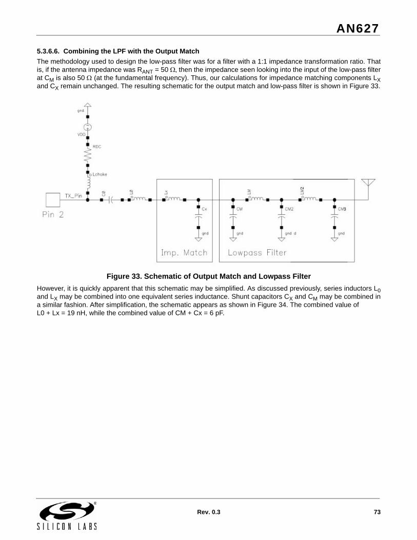
AN627
Rev. 0.3 73
5.3.6.6. Combining the LPF with the Output Match
The methodology used to design the low-pass filter was for a filter with a 1:1 impedance transformation ratio. Thatis, if the antenna impedance was RANT = 50 , then the impedance seen looking into the input of the low-pass filterat CM is also 50 (at the fundamental frequency). Thus, our calculations for impedance matching components LXand CX remain unchanged. The resulting schematic for the output match and low-pass filter is shown in Figure 33.
Figure 33. Schematic of Output Match and Lowpass Filter
However, it is quickly apparent that this schematic may be simplified. As discussed previously, series inductors L0and LX may be combined into one equivalent series inductance. Shunt capacitors CX and CM may be combined ina similar fashion. After simplification, the schematic appears as shown in Figure 34. The combined value of L0 + Lx = 19 nH, while the combined value of CM + Cx = 6 pF.

AN627
74 Rev. 0.3
Figure 34. Schematic of Output Match and Lowpass Filter (Simplified)
After the filtered class E Tx match is finalized, some bench tuning is also advisable. As mentioned earlier, duringthe adjustment process, it was seen that the efficiency can be improved slightly if the shunt (CM + Cx, which, in anycase, is denoted simply by CM in the tables in "2. Summary of Matching Network Component Values" on page 6)capacitor is reduced to 2.7 pF. Again, this sacrifices some second harmonic attenuation, but the harmonicspectrum still complies with a large margin (see Figure 35).
The final class E Split TX match component values are given for the Si4461 in Table 8 on page 13 and for theSi4060/Si4460 Table 13 on page 18.

AN627
Rev. 0.3 75
5.3.6.7. Final Measurement of Harmonic Spectrum of the 13 dBm Class E High-Efficiency Match
The conducted output power spectrum of the final circuit is shown in Figure 35. These results are measured at theTX output power level setting of 0x31 of the Si4060/Si4460 RFIC with 22.8 mA total current consumption at 3.2 Vsupply voltage. As can be seen, the output power is approximately 0.5 dB lower than that without a filter, i.e the reallossy filter attenuation is approximately 0.5 dB. However, due to the reduced CM, the efficiency improved, and thetotal IC current is only 22.8 mA.
Figure 35. Filtered Harmonic Spectrum at Power State 0x31 (with 22.8 mA Total IC Current) of the 13 dBm Si4060/Si4460 High-Efficiency Class E Match (Fo = 868 MHz—See Table 12 on page 17)

AN627
76 Rev. 0.3
5.3.6.8. Final Measurement of Harmonic Spectrum of the 10 dBm Class E Match
In theory, the 10 dBm Class E design should be the same as the 13 dBm one; only the power level is reducedproperly by a lower power level setting. However, during bench tweaking, it is seen that the efficiency at low powerlevels can be improved further if the C0 value is increased slightly. The conducted output power spectrum of thefinal 10 dBm circuit (given in Table 12 on page 17) is shown in Figure 36. These results are measured at the TXoutput power level setting of 0x19 of the Si4060/Si4460 RFIC with 16.4 mA total current consumption at 3.2 Vsupply voltage.
Figure 36. Filtered Harmonic Spectrum at Power State 19h of the Tuned 10 dBm Si4060/Si4460 Class E Match (Fo = 868 MHz—See Table 12 on page 17 for Component Values)
5.3.7. Summary of Match
This completes the steps of the match design process for the Split TX/RX board configuration. This match designprocess may be used to obtain matching component values at any desired operating frequency as well as for theSi4461. A summary table of these matching component values is shown in Tables 7 and 12.

AN627
Rev. 0.3 77
5.4. Detailed Matching Procedure for Direct Tie Board ConfigurationIn the Direct Tie board configuration, the TX and RX paths are tied directly together without the use of an RFswitch, as shown in Figure 37. Careful design procedure must be followed to ensure that the RX input circuitrydoes not load down the TX output path while in TX mode and that the TX output circuitry does not degrade receiveperformance while in RX mode.
The RX input circuitry of the EZRadioPRO 2 family of chips contains a set of switches that aids in isolation of theRX pins in TX mode. This set of switches is implemented internally as shown in Figure 37.
Figure 37. RX Input Switches for Direct Tie Operation
These three switches are activated simultaneously upon entering TX mode. They are opened only in RX mode andclosed during all other modes (including TX mode).
Here, the operation in TX mode (when the switchers are closed) is the same as what was described in the case ofthe SWC DT match (see "3.2.1. Concept of Direct Tie Matching" on page 41); closing these switches during TXmode effectively shorts the RXp and RXn input pins together and shorts them to GND. The effective circuit may beredrawn as shown in Figure 38. Note that inductor LR2 and capacitor CR2 have been placed in parallel by theclosure of the switches, and they are connected to GND. If the values of these components are chosen forresonance at the desired operating frequency, a very high impedance is presented to the TX path, resulting in verylittle degradation in TX output power. Also, by shorting the input pins of the LNA together and simultaneously toGND, the LNA is protected from the large signal swing of the TX signal. This feature allows connection of the TXpath to the RX path without damage to the LNA.

AN627
78 Rev. 0.3
Figure 38. Effective Direct Tie Circuit in TX Mode
In RX mode, the output transistors of the PA are in the OFF state, and the impedance seen looking back into theTX pin is comprised mostly of the output capacitance of the transistors. (The impedance of the pull-up inductor,LCHOKE, is quite high and may be ignored for this discussion.) This OFF stated PA output capacitance value,CPAOFF, is not much different from the ON STATED value. In the case of a Class E match, this PA capacitance iseffectively in-series with matching capacitor C0 and results in series-resonance with inductor L0 at somefrequency, as shown in Figure 39. At this series-resonant frequency, the input to the LNA matching network (LR2,CR2, LR, CR1) is effectively shorted to GND and thus significantly degrades receive performance. As the PAoutput capacitance, CPAOFF, is fixed, it is necessary to choose L0 and C0 to ensure that this series-resonance doesnot excessively degrade RX performance at the desired operating frequency. It may be necessary to alter thevalues of L0 (variation of C0 is less efficient as it is in-series with the fixed CPAOFF) slightly away from theircalculated optimum values in order to accomplish this goal, thus slightly degrading TX performance in an effort tominimize the impact to RX performance.
With the typical CPAOFF values of the Si4460/61 RFIC family, this effect is most critical at the upper frequencybands (868 or 915 MHz). At lower frequency bands (169 or 434 MHz) it usually does not cause any problems, andthe DT TX match element values are identical to the values of the Split TX/RX configuration.

AN627
Rev. 0.3 79
Figure 39. Effective Direct Tie Circuit in RX Mode
We next provide further detail about each step of the matching procedure for the Single Antenna with Direct Tieboard configuration. Again, assume a general chip supply voltage of VDD_RF = 3.3 V. Our design example will beconstructed for Si4460 for the 868 MHz ETSI band, with a targeted output power level of +13 dBm.
5.4.1. Steps #1–6: Same Design Procedure as for Split TX/RX Board Configuration
Steps 1 through 6 are exactly the same as those shown in "5.3. Detailed Matching Procedure for Split TX/RX BoardConfiguration" on page 58.

AN627
80 Rev. 0.3
5.4.2. Step #7: Design RX Input Match
In Step #7, we design an impedance matching network for the differential RX input. The RX matching network iscomprised of a total of four inductors and capacitors (LR2, CR2, LR, CR). The goals for this network are as follows:
Match the LNA input to a 50 source impedance (i.e., the antenna)
Provide a single-ended to differential conversion function (i.e., a balun)
Ensure that LR2,CR2 are parallel-resonant at the desired operating frequency
The design equations (and their mathematical derivation) for selection of the matching component values arediscussed in detail in “AN643 Si446x RX LNA Matching”. This procedure is also the same one described in "3.2.4.Construction of RX Match" on page 45. The following equations are introduced here without proof or furtherdiscussion; refer to AN643 for further details.
Equation 30.
Equation 31.
Equation 32.
Equation 33.
Equation 34.
Equation 35.
Note that our goal of parallel-resonance between LR2 and CR2 is inherently satisfied, as evidenced byEquation 31.
At any given frequency, the differential input impedance at the RX pins of the chip may be represented by anequivalent parallel R-C circuit; their values are represented by the parameters RLNA and CLNA in the aboveequations. It is necessary to know these equivalent circuit values at the desired frequency of operation, prior toconstructing the match.
The differential input impedance of the RX port on the Si446x RFIC is provided in AN643. The values of RLNA andCLNA at a desired operating frequency of 868 MHz are found to be RLNA = 380 and CLNA = 1.09 pF. Afterplugging these values into the above equations, the following ideal matching component values are calculated:
LR2 = 25.27 nH
CR2 = 1.33 pF
LR1 = 19.15 nH
CR1 = 2.66 pF
LR2
50 RLNARF
--------------------------------------=
CR21
RF2
LR2-----------------------------=
CR1 2 CR2=
LLNA1
RF2
CLNA----------------------------------=
LM 2 LR2=
LR1
LLNA LMLLNA LM+---------------------------=

AN627
Rev. 0.3 81
In practice, it is often necessary to slightly modify the matching component values suggested by the aboveequations. Any printed circuit board layout has parasitics, such as trace inductances or component padcapacitances, and these may have an effect upon the circuit. Silicon Labs has empirically determined that if 0402-size wire-wound or multilayer inductors are used on the Direct Tie reference board designs (available atwww.silabs.com), the actual component values are as shown in the 868 MHz rows in Table 14 on page 19 for thewire-wound case and reproduced below:
LR2 = 24 nH
CR2 = 1 pF
LR1 = 20 nH
CR1 = 3 pF
The above inductor element values are not available in multilayer type; so, new bench-optimized multilayer RXmatch elements are necessary and are given in Table 15 on page 19.
Although not required, it is useful to measure the input impedance seen looking into the RX match in both RX modeas well as TX mode. Obviously, it is desired to verify a good match to 50 while in RX mode in order to obtainoptimum sensitivity. However, it is also useful to verify that the network provides a high impedance while in TXmode (when the switches at the input of the LNA (see Figure 38) are in their CLOSED position, and thus LR2 andCR2 form a high-impedance parallel-resonant network, which isolates the RX path from the TX path); otherwise,the RX circuitry may excessively load down the TX path. Specifically, it may be necessary to slightly adjust thevalues of LR2 and/or CR2 to achieve optimum parallel resonance at the desired frequency of operation.
The isolation in TX mode is more critical with multilayer inductors since this type has lower Q (higher loss), and thevalues are available in rarer steps. So both to achieve high impedance at LR2-CR2 parallel resonance and also totune the resonance exactly to the frequency of operation is more difficult.
The actual measured impedance of the 868M multilayer RX match while in TX mode is shown in Figure 40 andconfirms the expectations of “good enough” isolation; the measured impedance at 868 MHz is ~452 + j593,which corresponds to a parallel R-C equivalent of 1.2 k – 0.196 pF. This slight parallel capacitance (~196 fF) maybe ignored.
Figure 40. RX Match Input Impedance in TX Mode, Multilayer 868M Type
The measured impedance at the input of the multilayer RX matching network while in RX mode is shown in

AN627
82 Rev. 0.3
Figure 41. It is observed that the input impedance is quite close to 50 , with the network providing S11 with betterthan 15 dB return loss.
Figure 41. RX Match Input Impedance in RX Mode, Multilayer 868M Type

AN627
Rev. 0.3 83
5.4.3. Step #8: Slightly Modify the Value of L0
In Step #8, we deliberately mistune the value of matching inductor L0 slightly away from its optimum value, asdetermined in Steps 1 through 6. As illustrated in Figure 39 on page 79, the series-resonance of L0-C0-CPAOFF hasthe potential to significantly degrade the RX performance by placing a (near) short to GND at the input of the RXmatching network. It is important that this series-resonant frequency be adjusted to fall sufficiently far away fromthe desired operating frequency in order to minimize its effect upon RX sensitivity.
This is accomplished by deliberately increasing or decreasing the value of L0. Here, the variation of C0 is notefficient as it is in series with the fixed CPAOFF; thus, higher deviation from the optimum class-E value would benecessary to achieve the same detuning.
In the 868/915 MHz band and in RX mode, the Si4461 usually needs to have L0 increased (compared to the splitTX/RX case) in order to shift away the L0-C0-CPAOFF parasitic resonance while, for the Si4460, the L0 usuallyneeds to be decreased in order to shift away the L0-C0-CPAOFF parasitic resonance.
This will push the unwanted resonance lower or higher in frequency and minimize its effect upon RX performance.A typical aim is to suffer less than 2 dB sensitivity degradation at direct tie mode compared to the split TX/RX case.
Some post-tuning of capacitor CM may also be required to improve Class-E operation in TX mode after the changein value of L0.
The value of PA output capacitance in its OFF state may be slightly different than the value of shunt draincapacitance CSHUNT (discussed in "5.3.3. Step #3: Calculate the Required Value for ZLOAD" on page 59). Thevalue of CPAOFF may be measured with a network analyzer connected to the TX output pin with all matchingcomponents removed, except for those providing dc bias (i.e., LCHOKE and RDC). Silicon Labs has performed thismeasurement and determined the value of CPAOFF to be ~1.5 pF in the frequency range of 868 MHz to 950 MHzand 1.4 pF at low bands (315/434M). This is shown by the impedance measurement of Figure 42. The value ofLCHOKE must be chosen appropriately to provide a very high impedance at the frequency of interest; otherwise, themeasured value of CPAOFF may be affected.
Figure 42. PA Output Capacitance Measurement of Si4460 in OFF State

AN627
84 Rev. 0.3
Once the value of CPAOFF has been determined, its effect upon RX performance may be estimated. Continuingwith our design example at 868 MHz with the 13 dBm wire-wound split TX/RX board design, we find initial values ofL0-C0 to be:
L0 = 19 nH
C0 = 3.6 pF
This value of capacitance of C0 is in series with CPAOFF = 1.5 pF, resulting in an equivalent series capacitance ofCEQUIV = 1.06 pF. The series-resonant behavior of the resulting L-C circuit may be simulated and is shown inFigure 43; here, the S21 of the TX path is simulated from the filter outputs to the DT point with the L0-C0-CPAOFFpart. It can be observed that this L0-C0-CPAOFF circuit introduces only ~0.8 dB of loss at 868 MHz, which is mostlythe filter attenuation. Since this circuit is directly connected to the input of the RX match, this will result inapproximately 0.8 dB of degradation in RX sensitivity, which is acceptable. It is also clear from the curve that thecritical shunt of the RX path occurs far above 1 GHz.
Figure 43. Series-Resonance Behavior of Initial L0-C0 Circuit of Si4460 13 dBm Split Class E Match
Unfortunately, the situation is more critical in case of the Si4460 10 dBm direct tie. There, the initial split C0 value ismuch higher (see Table 12 on page 17) in order to achieve better efficiency at reduced power levels. With the initialvalues of:
L0 = 19 nH
C0 = 15 pF
The parasitic L0-C0 – CPAOFF series resonance curve is shown in Figure 44. As can be observed, due to the higherC0, the resultant CEQUIV capacitance is 1.36 pF, and, thus, the resonance is at lower frequencies closer to theuseful band. It results in an attenuation of ~2.5 dB according to the simulations. In real bench circumstances, thedegradation in RX mode was even higher, approx 3.5 dB, which is unacceptable.
The resonant frequency of these circuit components may be shifted further upwards (away from the desiredoperating frequency) by decreasing the value of L0. Using our rule-of-thumb of decreasing L0 by ~20%, we arrive
0.000 500.000M 1.000G 1.500G 2.000G
-30.00
-22.50
-15.00
-7.50
0.00
f/Hz
Series- Resonant Effect of L0-C0-CPAOFF Si4460 868M 13dBm initial split match S21[dB]

AN627
Rev. 0.3 85
at a modified value of L0 = 15 nH. In theory, with the 20% L0 variation, the class E operation in TX mode is stillsatisfactory, and, usually, the sensitivity degradation in RX mode will improve to be less than ~2 dB. However, inthe case of the +10 dBm 868 MHz Si4460 DT match, the bench test of this modified circuit still did not showsufficiently good sensitivity in RX mode.
So, the L0 was decreased further to 12 nH with a parallel increase of C0 to keep the optimum class E TX operation.Simulation of the series-resonant behavior of the modified circuit is shown in Figure 45.
It is seen that the loss at 868 MHz has now been improved significantly to only ~0.9 dB in the simulations. In thebench test, the suffered RX sensitivity degradation is only ~1.1 dB, very close to the simulated value. While this stillrepresents a 1.2 dB reduction in RX sensitivity, this is a good compromise between TX and RX performance.
Although this (12 nH and 27 pF pls. see Table 14 on page 19) set of L0-C0 values is proper for 868M 10 dBmoperation, it is not good at 915M. Since dual band CLE TX operation seems to be feasible with minimumcompromise, it makes sense to create a dual band DT circuit as well.
To have good Rx sensitivity at 915M the L0-C0-CPAOFF resonance has to be shifted up further. So, the newproposed L0 value is 6.8 nH and the new C0 values is 36 pF (Table 14) to have both moderate Rx sensitivitydegradation at 915M and to maintain the acceptable TX class E operation at 868M and 915M.
Figure 44. Series-Resonance Behavior of the Off-Stated Si4460 PA with the Initial 10 dBm 868M Split Class E L0-C0 Circuit (19 nH–15 pF)
0.000 500.000M 1.000G 1.500G 2.000G
-30.00
-22.50
-15.00
-7.50
0.00
f/Hz
Series- Resonant Effect of L0-C0-CPAOFF Si4460 868M 10dBm initial split match S21[dB]

AN627
86 Rev. 0.3
Figure 45. Series-Resonance Behavior of the Off-Stated Si4460 PA with the modified 868M 10 dBm Split Class E L0-C0 Circuit (12 nH–27 pF)
It is also possible to increase the resonant frequency of the L0-C0-CPAOFF circuit by decreasing the value of C0instead of L0. Here, it important to note that the increase of the C0 capacitor will have a reduced effect on theparasitic series-resonant frequency since the value of CPAOFF is significantly lower than that of C0, and, thus,CPAOFF determines primarily the resonance. Hence, a much larger increase of C0 is required to achieve the sameresonance shift. This stronger mistuning will result in even greater reduction in performance in TX mode.Therefore, tuning of L0 is preferred and generally results in a better compromise between TX and RX performance.
This increase in the value of L0 is usually required only when working in the upper frequency bands, such as 868/915/950 MHz. In the lower frequency bands (315/390/434 MHz), the values of L0 and C0 obtained for the Split TX/RX board configuration usually continue to work well with the Direct Tie board configuration.
In the final circuit realization on Silicon Labs reference design boards, the value of capacitor CM was reduced to1.5 pF to provide slightly better TX output power. The final Si4460 element values with wire-wound inductors aresummarized in Table 14 on page 19. For Multilayer inductors, the same is given in Table 15 on page 19.
For the Si4461, the DT board element values are summarized in Tables 9, 10, and 12, both for wire-wound andmultilayer inductor types.
Note that some small degradation in both TX and RX performance is expected for a Direct Tie configuration. Thatis, it is not possible to directly connect the TX and RX paths and achieve perfect isolation between the two circuitfunctions; each path will result in some amount of unwanted loading to the other path, and, thus, some there will beslight degradation in performance (relative to a Split TX/RX board configuration in which the TX and RX pathsremain entirely separate). The choice of matching inductor L0 heavily impacts the trade-off between optimizing forTX output power at the expense of degraded RX sensitivity, or vice-versa. A value may generally be found thatachieves a good compromise between the two, typically resulting in less than 1 dB reduction in TX output powerand no more than 2–3 dB reduction in RX sensitivity. Some amount of “tweaking” of the final values of L0 and CMmay be necessary to achieve the best compromise.
5.4.4. Summary of Match
This completes the steps of the match design process for the Direct Tie board configuration. This match designprocess may be used to obtain matching component values at any desired operating frequency.
0.000 500.000M 1.000G 1.500G 2.000G
-30.00
-22.50
-15.00
-7.50
0.00
f/Hzmagdb(S(2,1)) magdb(S(1,2))magdb(S(2,1)) magdb(S(1,2))
Series- Resonant Effect of L0-C0-CPAOFF Si4460 868M 10dBm of Modified DT match S21[dB]

AN627
Rev. 0.3 87
APPENDIX A—MEASURED SPECTRUM PLOTS
The following section presents some measured spectral data plots on different CLE board configurations in TXmode at a variety of frequencies given in "2. Summary of Matching Network Component Values" on page 6.Measured results for circuit realizations with both wire-wound inductors and multi-layer inductors are presented.
Si4461 Measured Plots
Si4461 Split TX/RX Board CLE Configurations with Wire-Wound Inductors
Figure 46. Si4461 14 dBm Split TX/RX Board at 434 MHz with Wire-Wound Inductors, VDD = 3.2 V, DDAC[6:0] Field in the PA_PWR_LVL Register is 0x20, 28.1 mA

AN627
88 Rev. 0.3
Figure 47. Si4461 16 dBm Split TX/RX Board at 434 MHz with Wire-Wound Inductors, VDD = 3.2 V, DDAC[6:0] field in the PA_PWR_LVL register is 0x32, 35.8 mA

AN627
Rev. 0.3 89
Figure 48. Si4461 14 dBm Split TX/RX Board at 868 MHz with Wire-Wound Inductors, VDD = 3.2 V, DDAC[6:0] field in the PA_PWR_LVL register is 0x2B, 31.6 mA

AN627
90 Rev. 0.3
Figure 49. Si4461 16 dBm Split TX/RX Board at 868 MHz with Wire-Wound Inductors, VDD = 3.2 V, DDAC[6:0] field in the PA_PWR_LVL register is 0x40, 38.9 mA

AN627
Rev. 0.3 91
Si4461 Split TX/RX Board CLE Configurations with Multilayer Inductors
Figure 50. Si4461 14 dBm Split TX/RX Board at 434 MHz with Multilayer Inductors, VDD = 3.2 V, DDAC[6:0] field in the PA_PWR_LVL register is 0x2D, 29.7 mA
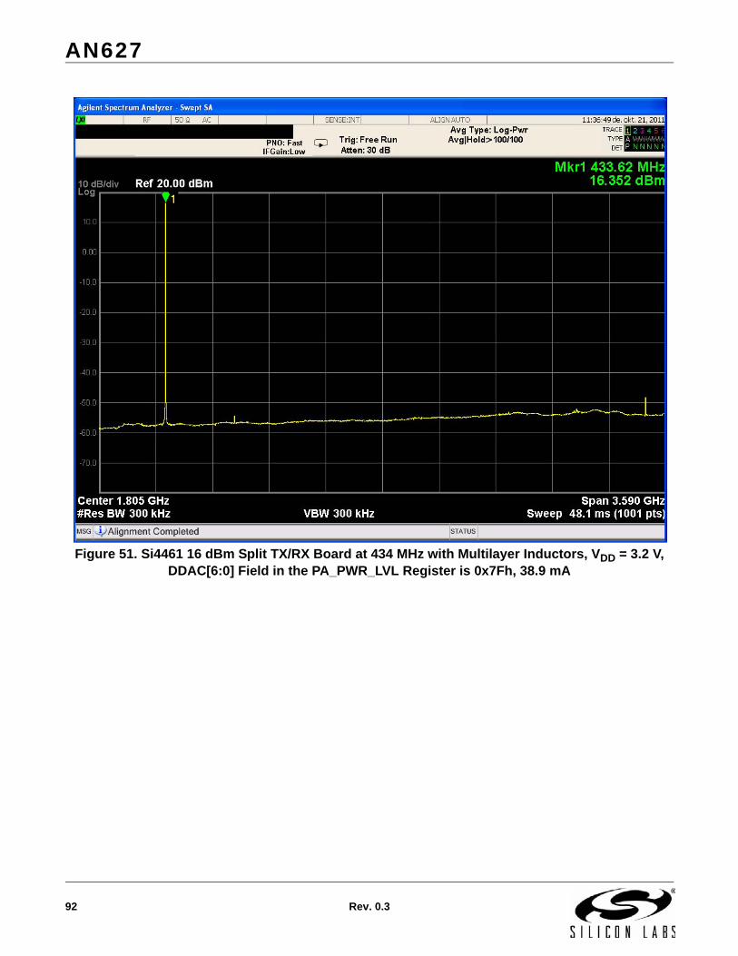
AN627
92 Rev. 0.3
Figure 51. Si4461 16 dBm Split TX/RX Board at 434 MHz with Multilayer Inductors, VDD = 3.2 V, DDAC[6:0] Field in the PA_PWR_LVL Register is 0x7Fh, 38.9 mA

AN627
Rev. 0.3 93
Figure 52. Si4461 14 dBm Split TX/RX Board at 868 MHz with Multilayer Inductors, VDD = 3.2 V, DDAC[6:0] field in the PA_PWR_LVL Register is 0x34, 34.4 mA

AN627
94 Rev. 0.3
Figure 53. Si4461 16 dBm Split TX/RX Board at 868 MHz with Multilayer Inductors, VDD = 3.2 V, DDAC[6:0] Field in the PA_PWR_LVL Register is 0x4F, 42.7 mA

AN627
Rev. 0.3 95
Si4461 Direct Tie TX/RX Board CLE Configurations with Wire-Wound Inductors
Figure 54. Si4461 14 dBm Direct Tie TX/RX Board at 434 MHz with Wire-Wound Inductors, VDD = 3.2 V, DDAC[6:0] Field in the PA_PWR_LVL Register is 0x21, 28.7 mA

AN627
96 Rev. 0.3
Figure 55. Si4461 16 dBm Direct Tie TX/RX Board at 434 MHz with Wire-Wound Inductors, VDD = 3.2 V, DDAC[6:0] Field in the PA_PWR_LVL Register is 0x31, 33 mA

AN627
Rev. 0.3 97
Figure 56. Si4461 14 dBm Direct Tie TX/RX Board at 868 MHz with Wire-Wound Inductors, VDD = 3.2 V, DDAC[6:0] Field in the PA_PWR_LVL Register is 0x2E, 33.2 mA

AN627
98 Rev. 0.3
Figure 57. Si4461 16 dBm Direct Tie TX/RX Board at 868 MHz with Wire-Wound Inductors, VDD = 3.2 V, DDAC[6:0] field in the PA_PWR_LVL Register is 0x41, 39.6 mA

AN627
Rev. 0.3 99
Si4461 Direct Tie TX/RX Board CLE Configurations with Multilayer Inductors
Figure 58. Si4461 14 dBm Direct Tie TX/RX Board at 434 MHz with Multilayer Inductors, VDD = 3.2 V, DDAC[6:0] Field in the PA_PWR_LVL Register is 0x2F, 30.1 mA

AN627
100 Rev. 0.3
Figure 59. Si4461 16 dBm Direct Tie TX/RX Board at 434 MHz with Multilayer Inductors, VDD = 3.2V, DDAC[6:0] Field in the PA_PWR_LVL Register is 0x7F, 40.1 mA

AN627
Rev. 0.3 101
Figure 60. Si4461 14 dBm Direct Tie TX/RX Board at 868 MHz with Multilayer Inductors, VDD = 3.2 V, DDAC[6:0] Field in the PA_PWR_LVL Register is 0x34, 34.4 mA

AN627
102 Rev. 0.3
Figure 61. Si4461 16dBm Direct Tie TX/RX Board at 868 MHz with Multilayer Inductors, VDD = 3.2 V, DDAC[6:0] Field in the PA_PWR_LVL Register is 0x5E, 42.9 mA

AN627
Rev. 0.3 103
Si4060/Si4460 Measured Plots
Si4060/Si4460 Split TX/RX Board CLE Configurations with Wire-Wound Inductors
Figure 62. Si4060/Si4460 10 dBm Split TX/RX Board at 434 MHz with Wire-Wound Inductors, VDD = 3.2 V, DDAC[6:0] Field in the PA_PWR_LVL Register is 0x19, 16.9 mA

AN627
104 Rev. 0.3
Figure 63. Si4060/Si4460 13 dBm Split TX/RX Board at 434 MHz with Wire-Wound Inductors, VDD = 3.2 V, DDAC[6:0] Field in the PA_PWR_LVL Register is 0x3F, 22.7 mA

AN627
Rev. 0.3 105
Figure 64. Si4060/Si4460 10 dBm Split TX/RX Board at 868 MHz with Wire-Wound Inductors, VDD = 3.2 V, DDAC[6:0] Field in the PA_PWR_LVL Register is 0x19h, 16.4 mA

AN627
106 Rev. 0.3
Figure 65. Si4060/Si4460 14 dBm Split TX/RX Board at 868 MHz with Wire-Wound Inductors, VDD = 3.2 V, DDAC[6:0] Field in the PA_PWR_LVL Register is 0x3Dh, 24.8 mA
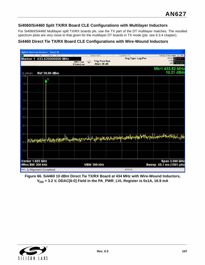
AN627
Rev. 0.3 107
Si4060/Si4460 Split TX/RX Board CLE Configurations with Multilayer InductorsFor Si4060/Si4460 Multilayer split TX/RX boards pls. use the TX part of the DT multilayer matches. The resultedspectrum plots are very close to that given for the multilayer DT boards in TX mode (pls. see 6.3.4 chapter).
Si4460 Direct Tie TX/RX Board CLE Configurations with Wire-Wound Inductors
Figure 66. Si4460 10 dBm Direct Tie TX/RX Board at 434 MHz with Wire-Wound Inductors, VDD = 3.2 V, DDAC[6:0] Field in the PA_PWR_LVL Register is 0x1A, 16.9 mA

AN627
108 Rev. 0.3
Figure 67. Si4460 13 dBm HP Direct Tie TX/RX Board at 434 MHz with Wire-Wound Inductors, VDD = 3.2 V, DDAC[6:0] Field in the PA_PWR_LVL Register is 0x3F, 23 mA

AN627
Rev. 0.3 109
Figure 68. Si4460 10 dBm 868–915M Direct Tie TX/RX Board at 868 MHz with Wire-Wound Inductors, VDD = 3.2 V, DDAC[6:0] Field in the PA_PWR_LVL Register is 0x20, 19.7 mA

AN627
110 Rev. 0.3
Figure 69. Si4460 10 dBm 868–915M Direct Tie TX/RX Board at 915 MHz with Wire-Wound Inductors, VDD = 3.2 V, DDAC[6:0] Field in the PA_PWR_LVL Register is 0x20, 20 mA

AN627
Rev. 0.3 111
Figure 70. Si4460 868-915M Direct Tie TX/RX Board at 868 MHz at Max Power State with Wire-Wound Inductors, VDD = 3.2 V, DDAC[6:0] Field in the PA_PWR_LVL Register is 0x4F, 25.5 mA

AN627
112 Rev. 0.3
Figure 71. Si4460 868–915M Direct Tie TX/RX Board at 915 MHz at Max Power State with Wire-Wound Inductors, VDD = 3.2 V, DDAC[6:0] Field in the PA_PWR_LVL Register is 0x4F, 24.7 mA

AN627
Rev. 0.3 113
Figure 72. Si4460 14 dBm Direct Tie HP TX/RX Board at 868 MHz with Wire-Wound Inductors, VDD = 3.2 V, DDAC[6:0] Field in the PA_PWR_LVL Register is 0x44, 25.6 mA

AN627
114 Rev. 0.3
Si4460 Direct Tie TX/RX Board CLE Configurations with Multilayer Inductors
Figure 73. Si4460 10 dBm Direct Tie TX/RX Board at 434 MHz with Multilayer Inductors, VDD = 3.2 V, DDAC[6:0] Field in the PA_PWR_LVL Register is 0x2A, 17.1 mA

AN627
Rev. 0.3 115
Figure 74. Si4460 12.3 dBm Direct Tie HP TX/RX Board at 434 MHz with Multilayer Inductors, VDD = 3.2 V, DDAC[6:0] Field in the PA_PWR_LVL Register is 0x4F, 23.1 mA

AN627
116 Rev. 0.3
Figure 75. Si4460 10 dBm 868–915M Direct Tie TX/RX Board at 868 MHz with Multilayer Inductors, VDD = 3.2 V, DDAC[6:0] Field in the PA_PWR_LVL Register is 0x20, 19.7 mA

AN627
Rev. 0.3 117
Figure 76. Si4460 10 dBm 868–915M Direct Tie TX/RX Board at 915 MHz with Wire-Wound Inductors, VDD = 3.2 V, DDAC[6:0] Field in the PA_PWR_LVL Register is 0x20, 19.3 mA

AN627
118 Rev. 0.3
Figure 77. Si4460 868–915M Direct Tie TX/RX Board at 868 MHz at Max Power State with Multilayer Inductors, VDD = 3.2 V, DDAC[6:0] Field in the PA_PWR_LVL Register is 0x4F, 24.7 mA
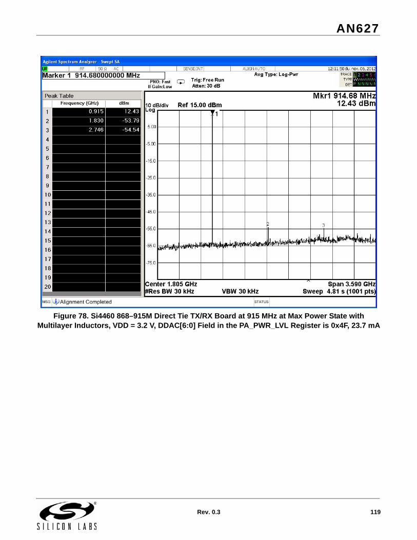
AN627
Rev. 0.3 119
Figure 78. Si4460 868–915M Direct Tie TX/RX Board at 915 MHz at Max Power State with Multilayer Inductors, VDD = 3.2 V, DDAC[6:0] Field in the PA_PWR_LVL Register is 0x4F, 23.7 mA
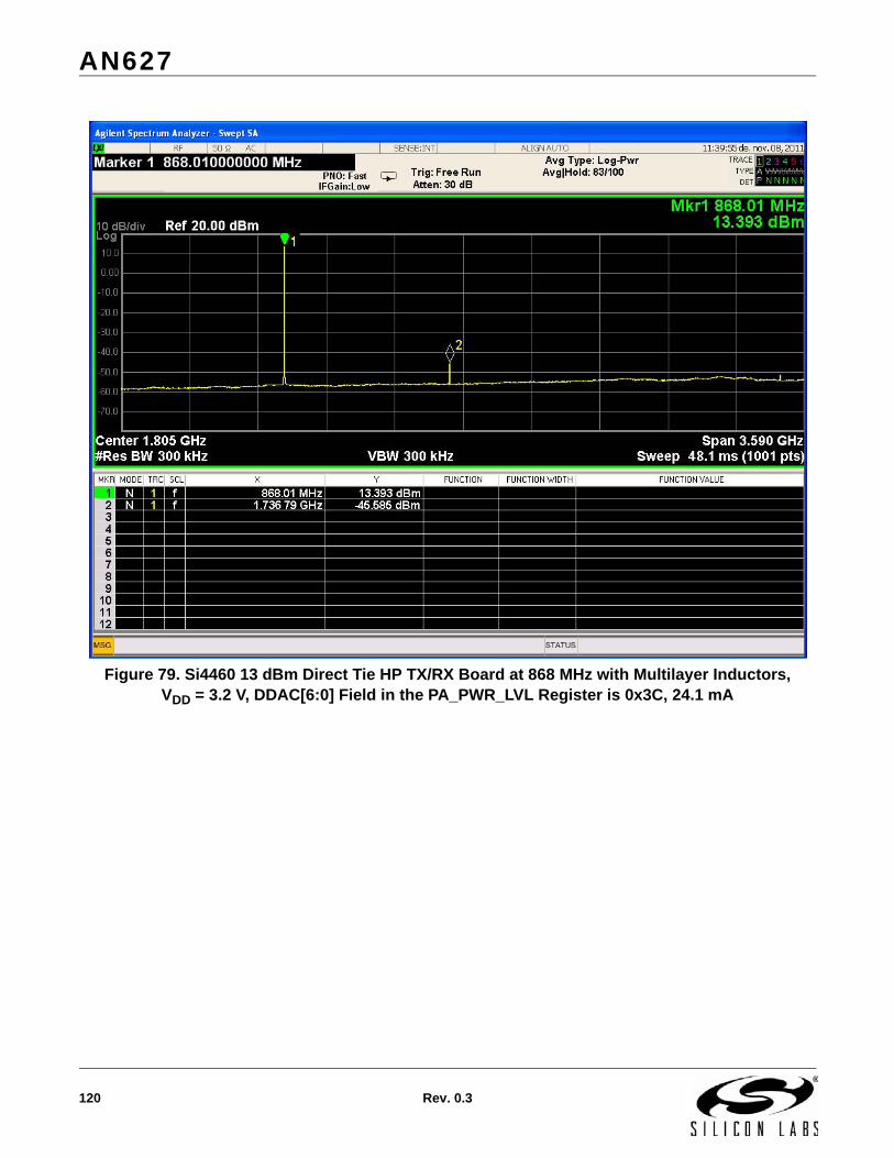
AN627
120 Rev. 0.3
Figure 79. Si4460 13 dBm Direct Tie HP TX/RX Board at 868 MHz with Multilayer Inductors, VDD = 3.2 V, DDAC[6:0] Field in the PA_PWR_LVL Register is 0x3C, 24.1 mA

AN627
Rev. 0.3 121
Figure 80. Si4460 10 dBm Direct Tie TX/RX Board at 169 MHz with Multilayer Inductors, VDD = 3.2 V, DDAC[6:0] Field in the PA_PWR_LVL Register is 0x23, 18.4 mA

AN627
122 Rev. 0.3
DOCUMENT CHANGE LIST
Revision 0.1 to Revision 0.2Revised "1. Introduction" on page 1.
Revised "2. Summary of Matching Network Component Values" on page 6.
Added "4. Class E (CLE) Matching Procedure Overview" on page 50.
Added "5. CLE Matching Procedure for the Si4060/Si4460/61" on page 56.
Added " Appendix A—Measured Spectrum Plots" on page 87.
Revision 0.2 to Revision 0.3Added " Table of Contents" on page 4.
Extended introduction with more detailed descriptions.
Updated "2.1.2. Si4461 with Direct Tie TX/RX SWC Board Configuration: Component Values and Performance" on page 9.Added a new 868M Si4461 SWC DT Match
(FC868M) with flat Pout vs. Vdd characteristic in new Tables 4 and 5 in this section.
Added Table 6 in this section.
Added description of 25% duty cycle PA mode used in Si4460 Class E matches in "2.2. Component Values for Si4060/Si4460 Matchings" on page 17.
New 10 dBm Si4460 Class E 868/915M dual band DT match (old 10 dBm 868M Class E DT eliminated) given in new Tables 14, 15, and 17 (element values and measured results).
Added Table 18, “Output Power, Current Consumption vs. Vdd (Direct Tie Si4460 434M CLE Board, WW Inductors),” on page 22.
Added "2.2.3. Si4060/4460 with Split TX\RX SWC Board Configuration: Component Values and Performance" on page 23.
Added "2.2.4. Si4460 with Direct Tie TX/RX SWC Board Configuration: Component Values and Performance" on page 23.
New Tables 19, 20, and 21.
Added Figure 8, “Matching Topology for Single Antenna with Direct Tie SWC Board Configuration,” on page 25.
Updated " Appendix A—Measured Spectrum Plots" on page 87.Added new Figures 68–71 and 75–78.
AN627
Rev. 0.3 123
NOTES:

AN627
124 Rev. 0.3
CONTACT INFORMATIONSilicon Laboratories Inc.
400 West Cesar ChavezAustin, TX 78701Tel: 1+(512) 416-8500Fax: 1+(512) 416-9669Toll Free: 1+(877) 444-3032
Please visit the Silicon Labs Technical Support web page:https://www.silabs.com/support/pages/contacttechnicalsupport.aspxand register to submit a technical support request.
Patent NoticeSilicon Labs invests in research and development to help our customers differentiate in the market with innovative low-power, small size, analog-intensive mixed-signal solutions. Silicon Labs' extensive patent portfolio is a testament to our unique approach and world-class engineering team.
Silicon Laboratories and Silicon Labs are trademarks of Silicon Laboratories Inc.Other products or brandnames mentioned herein are trademarks or registered trademarks of their respective holders.
The information in this document is believed to be accurate in all respects at the time of publication but is subject to change without notice. Silicon Laboratories assumes no responsibility for errors and omissions, and disclaims responsibility for any consequences resulting from the use of information included herein. Additionally, Silicon Laboratories assumes no responsibility for the functioning of undescribed fea-tures or parameters. Silicon Laboratories reserves the right to make changes without further notice. Silicon Laboratories makes no warran-ty, representation or guarantee regarding the suitability of its products for any particular purpose, nor does Silicon Laboratories assume any liability arising out of the application or use of any product or circuit, and specifically disclaims any and all liability, including without limitation consequential or incidental damages. Silicon Laboratories products are not designed, intended, or authorized for use in applications intend-ed to support or sustain life, or for any other application in which the failure of the Silicon Laboratories product could create a situation where personal injury or death may occur. Should Buyer purchase or use Silicon Laboratories products for any such unintended or unauthorized application, Buyer shall indemnify and hold Silicon Laboratories harmless against all claims and damages.