OVT CameraChip OV9620/9120 - Freemxhaard.free.fr/spca50x/Doc/Omnivision/ov9620_v2.0.pdfand an...
24
CAMERACHIP™ DATASHEET CameraChip™ Datasheet Datasheet – OV9620/9120 © OmniVision Technologies Inc., 2002 OVT CameraChip OV9620/9120 Last Modified: 22 February 2002 Revised Version: 2.0 THIS DOCUMENT IS PROVIDED “AS IS” WITH NO WARRANTIES WHATSOEVER, INCLUDING ANY WARRANTY OF MERCHANTABILITY, NON-INFRINGEMENT, FITNESS FOR ANY PARTICULAR PURPOSE, OR ANY WARRANTY OTHERWISE ARISING OUT OF ANY PROPOSAL, SPECIFICATION OR SAMPLE. OmniVision Technologies Inc. disclaims all liability, including liability for infringement of any proprietary rights, relating to use of information in this document. No license, expressed or implied, by estoppel or otherwise, to any intellectual property rights is granted herein. *Third-party brands, names, and trademarks are the property of their respective owners. Note: The information contained in this document is considered proprietary to OmniVision Technologies Inc. This information may be distributed only to individuals or organizations authorized by OmniVision Technologies, Inc. to receive said information. Individuals and/or organizations are not allowed to re-distribute said information without consent of OmniVision Technologies Inc. authorized representative(s).
Transcript of OVT CameraChip OV9620/9120 - Freemxhaard.free.fr/spca50x/Doc/Omnivision/ov9620_v2.0.pdfand an...

CAMERACHIP™ DATASHEET
CameraChip™ Datasheet Datasheet – OV9620/9120 © OmniVision Technologies Inc., 2002
OVT CameraChip OV9620/9120
Last Modified: 22 February 2002 Revised Version: 2.0
THIS DOCUMENT IS PROVIDED “AS IS” WITH NO WARRANTIES WHATSOEVER, INCLUDING ANY WARRANTY OF MERCHANTABILITY, NON-INFRINGEMENT, FITNESS FOR ANY PARTICULAR PURPOSE, OR ANY WARRANTY OTHERWISE ARISING OUT OF ANY PROPOSAL, SPECIFICATION OR SAMPLE. OmniVision Technologies Inc. disclaims all liability, including liability for infringement of any proprietary rights, relating to use of information in this document. No license, expressed or implied, by estoppel or otherwise, to any intellectual property rights is granted herein. *Third-party brands, names, and trademarks are the property of their respective owners.
Note: The information contained in this document is considered proprietary to OmniVision Technologies Inc. This information may be distributed only to individuals or organizations authorized by OmniVision Technologies, Inc. to receive said information. Individuals and/or organizations are not allowed to re-distribute said information without consent of OmniVision Technologies Inc. authorized representative(s).

OV9620/OV9120 DATASHEET
OmniVision Technologies, Inc. 930 Thompson Place Sunnyvale, CA 94085 Doc #DS102 Tel: (408) 733-3030 Fax: (408) 733-3061 Version 2.0 Email: [email protected] Website: http://www.ovt.com Page 1
Table of Contents
Table of Contents ................................................................................................................................................................................. 1 Description............................................................................................................................................................................................ 2 Features ............................................................................................................................................................................................... 2 Applications .......................................................................................................................................................................................... 2 Key Specifications ................................................................................................................................................................................ 2 Ordering Information............................................................................................................................................................................. 2 Pin Descriptions.................................................................................................................................................................................... 3 Electrical and Mechanical Characteristics ............................................................................................................................................ 4 Function Descriptions ........................................................................................................................................................................... 6
Image Capture and Processing Flow ................................................................................................................................................ 6 Image Processing ............................................................................................................................................................................. 7 Windowing ........................................................................................................................................................................................ 7 Sub-sampling Mode .......................................................................................................................................................................... 7
Progressive Sub-sampling............................................................................................................................................................. 7 Frame Exposure Mode ..................................................................................................................................................................... 8
Frame exposure Mode1: (One frame output) ................................................................................................................................ 8 Frame exposure Mode2: (Two frame output) ................................................................................................................................ 8
Frame Rate Adjust .......................................................................................................................................................................... 10 Frame Division ................................................................................................................................................................................ 10 Slave Mode Operation .................................................................................................................................................................... 10 Channel Average Calculator ........................................................................................................................................................... 10 Interface for External RAM Controller ............................................................................................................................................. 10 Reset .............................................................................................................................................................................................. 11 Power-Down Mode ......................................................................................................................................................................... 11 Configuring OV9620/OV9120 ......................................................................................................................................................... 11
Video Output....................................................................................................................................................................................... 12 RGB Raw Data Output.................................................................................................................................................................... 12 B/W Output ..................................................................................................................................................................................... 12 Digital Video Port ............................................................................................................................................................................ 12
MSB/LSB Swap........................................................................................................................................................................... 12 Line/Pixel Timing ......................................................................................................................................................................... 12 Pixel Output Pattern .................................................................................................................................................................... 13 Frame Timing .............................................................................................................................................................................. 13
Register Set........................................................................................................................................................................................ 15 OV9620/OV9120 Package Information .............................................................................................................................................. 21 Revision History.................................................................................................................................................................................. 23

OV9620/OV9120 DATASHEET
OmniVision Technologies, Inc. 930 Thompson Place Sunnyvale, CA 94085 Doc #DS102 Tel: (408) 733-3030 Fax: (408) 733-3061 Version 2.0 Email: [email protected] Website: http://www.ovt.com Page 2
Description The OV9620 (color) and OV9120 (black and white) are high-performance 1.3 mega-pixel CameraChips for digital still image and video camera products.
Both devices incorporate a 1280x1024(SXGA) image array and an on-chip 10-bit A/D converter capable of operating at up to 15 frames per second (FPS) with full resolution. Proprietary sensor technology utilizes advanced algorithms to cancel Fixed Pattern Noise (FPN), eliminate smearing, and drastically reduce blooming. The control registers allow for flexible control of timing, polarity, and CameraChip operation, which in turn allow the engineer a great deal of freedom in product design.
Features Optical Black Level Calibration Video or Snapshot Operations Programmable/Auto Exposure and Gain Control Programmable/Auto White Balance Control Horizontal & Vertical Sub-sampling (4:2 & 4:2) Programmable Image Windowing Variable Frame Rate Control On-Chip R/G/B Channel and Luminance Average Counter Internal/External Frame Synchronization SCCB Slave Interface Power on Reset and Power Down Mode
Figure 1. OV9620/OV9120 Pin Diagram
OV9620OV912048 LCC
(top View)
1 53 7
9
11
17
15
13
31
39
37
35
33
41
43 45 47NC
VSYNC
CHSYNC
HREF
DOGND
DOVDD
D9
D8
D7
D6
D5
PCLK
SIO
_C
SIO
_D
SCCB_E
PWDN
FREX
NCNC
FSIN
VcCHG
AVDD
AGND
ASUB
VrH
IGH
VrLO
W
NB
IT
RESET
SVD
D
SGN
D
DEG
ND
DEV
DD
VrA
D2
AD
VDD
AD
GN
D
D0
D1
D2
D3
D4
XCLK
1
XCLK
2
DVD
D
DG
ND
VGA
EXPSTB
SRAMT
VcC
HG
192123252729
Applications . Digital Still Camera . PC Camera/Dual Mode . Video Conference . Machine Vision . Security Cameras . Biometrics
Key Specifications Array Element(SXGA)
(VGA) 1280x1024
640x480
Pixel Size 5.2µm x 5.2µm Image Area 6.66mm x 5.32mm
Lens Size 1/2” Output 10-bit Digital RGB Raw Data
Max Frames/Sec (SXGA)
(VGA)
15FPS
30 FPS
Electronics Exposure (SXGA)
(VGA)
Up to 1050:1 Up to 500:1
Scan Mode Progressive Gamma Correction N/A
Sensitivity 1V/Lux-sec (B/W) S/N Ratio 54 dB
FPN < 0.03% VPP Dark Current 28mV/s
Dynamic Range 60 dB (due to ADC limitations) Power Supply 3.3VDC and 2.5VDC (+/- 5%)
Power Requirements < 50mA Active < 10µA Standby
Package 48 pin LCC
Ordering Information Product Package Description
OV9620 48 LCC
0.560 in2
COLOR, SXGA, VGA, Digital, SCCB interface
OV9120 48 LCC
0.560 in2
B/W, SXGA, VGA, Digital, SCCB interface

DATASHEET
OV9620/OV9120 Datasheet Doc #DS102
© OmniVision Technologies Inc., 2002, version 2.0 Page 3
Pin Descriptions Table 1. Pin Description Pin No. Name Pin Type Function/Description
01 SVDD P 3.3 volt supply for the pixel array 02 VrHigh A Sensor high reference. Bypass to ground with a 0.1µF capacitor 03 NBIT A Sensor bit line reference. Bypass to ground with a 0.1µF capacitor 04 DEVDD P 3.3 volt supply for sensor array decoder 05 DEGND P Ground for sensor array decoder 06 VrLow A Sensor low reference. Bypass to ground with a 0.1µF capacitor. 07 PWDN I (0) Power down mode enable, active high. 08 FREX I (0) Snapshot trigger, use to activate a snapshot sequence. 09 SRAMT I (0) SRAM interface trigger, use to activate SRAM interface. 10 RESET I (0) Chip reset, active high. 11 SCCB_E I (0) SCCB interface enable signal, active low. 12 EXPSTB I (0) Snapshot exposure start trigger, “1” – sensor stays in reset mode, “0” – sensor
starts exposure. Only effect in snap-shot mode. 13 VGA I (0) Sensor resolution selection.”1” – VGA. “0” – SXGA resolution. 14 FSIN I (0) Frame synchronization input. 15 VcCHG A Sensor reference. Bypass to ground with a 0.1µF capacitor. 16 AVDD P 3.3-volt supply for analog circuits. 17 AGND P Ground for analog circuits. 18 ASUB P Ground for analog circuit’s substrate. 19 VrAD2 A A/D converter reference. Bypass to ground with a 0.1µF capacitor. 20 ADVDD P 3.3-volt supply for A/D converter. 21 ADGND P Ground for A/D converter. 22 DVDD P 2.5-volt supply for digital circuits. 23 DGND P Ground for digital circuits. 24 D0 O Bit 0 of video port output. 25 D1 O Bit 1 of video port output. 26 D2 O Bit 2 of video port output. 27 D3 O Bit 3 of video port output. 28 D4 O Bit 4 of video port output. 29 XCLK1 I Crystal clock input. 30 XCLK2 O Crystal clock output. 31 PCLK O Pixel clock output. 32 D5 O Bit 5 of video port output. 33 D6 O Bit 6 of video port output. 34 D7 O Bit 7 of video port output. 35 D8 O Bit 8 of video port output. 36 D9 O Bit 9 of video port output. 37 DOVDD P 3.3-volt supply for digital video port. 38 DOGND P Ground for digital video port. 39 HREF I/O Horizontal reference output. 40 CHSYNC I/O Horizontal synchronization output when chip in master mode. Horizontal
synchronization input when chip in slave mode. 41 VSYNC I/O Vertical synchronization output when chip in master mode. Vertical synchronization
input when chip in slave mode. 42 NC - Not connected 43 NC - Not connected 44 NC - Not connected 45 SIO_D I/O SCCB slave interface data input and output. 46 SIO_C I SCCB slave interface clock input 47 VcCHG A Sensor reference. Bypass to ground through 0.1µF capacitor 48 SGND P Ground for pixel array. Legend: (I=Input), (O=Output), (I/O=Bi-directional), (P=Power), (A=Analog)

DATASHEET
OV9620/OV9120 Datasheet Doc #DS102
© OmniVision Technologies Inc., 2002, version 2.0 Page 4
Electrical and Mechanical Characteristics Table 2. General Characteristics
Descriptions Min Max Units Operating temperature 0 40 °C Storage temperature -40 125 °C Operating humidity TBD TBD Storage humidity TBD TBD
Table 3. DC Characteristics (0°C ≤ TA ≤ 85°C, Voltages referenced to GND)
Symbol Descriptions Max Typ Min Units Supply VDD1 Supply voltage
(DEVDD, ADVDD, AVDD, SVDD) 3.6 3.3 3.0 V
VDD2 Supply voltage (DOVDD) 3.6 3.3 3.0 V VDD3 Supply voltage (DVDD) 2.75 2.5 2.25 IDD1 Supply current
(SXGA@15Hz frame rate and 3.3V digital I/O with 25pF plus 1TTL loading on 10-bit data bus)
60 mA
IDD2 Supply current (VDD=3V, @15Hz frame rate without digital I/O loading)
40
IDD3 Standby supply current 15 10 Digital Inputs VIL Input voltage LOW 0.8 V VIH Input voltage HIGH 2 V CIN Input capacitor 10 pF Digital Outputs (standard loading 25pF, 1.2KΩ to 3V) VOH Output voltage HIGH 2.4 V VOL Output voltage LOW 0.6 V SCCB Input VIL SIO_C and SIO_D 1 0 -0.5 V VIH SIO_C and SIO_D VDD+0.5 3.3 2.5 V
Table 4. AC Characteristics (TA=25°C, VDD=3V)
Symbol Descriptions Max Typ Min Units ADC Parameters B Analog bandwidth 12 MHz DLE DC differential linearity error 0.5 LSB ILE DC integral linearity error 1 LSB settling time for hardware reset <1 ms settling time for software reset <1 ms settling time for VGA/XSGA mode change <1 µA settling time for register setting <300 ms
Table 5. Timing Characteristics
Symbol Descriptions Max Typ Min Units Oscillator and Clock Input fOSC Frequency (XCLK1,XCLK2) 48 24 8 MHz tr, tf Clock input rise/fall time 2 ns Clock input duty cycle 55 50 45 %

DATASHEET
OV9620/OV9120 Datasheet Doc #DS102
© OmniVision Technologies Inc., 2002, version 2.0 Page 5
Figure 2. OV9620/9120 Light Response
OV-9620spectrum response
0
20
40
60
80
100
120
140
160
180
200
300n
m
380n
m
420n
m
460n
m
500n
m
540n
m
580n
m
620n
m
660n
m
700n
m
740n
m
780n
m
820n
m
860n
m
900n
m
940n
m
980n
m
1020
nm
1060
nm
1100
nm
1180
nm
Wavelength
Sens
itivi
ty
R G B
Monochrome Response
0.000.100.200.300.400.500.600.700.800.901.00
400
450
500
550
600
650
700
750
800
850
900
950
1000
1050
1100
1150
Wavelength
Effic
ienc
y

DATASHEET
OV9620/OV9120 Datasheet Doc #DS102
© OmniVision Technologies Inc., 2002, version 2.0 Page 6
Function Descriptions This section describes the functions of the OV9620/9120.
Figure 3. OV9620/OV9120 Block Diagram
Timing Generator and Control Logic
Image Array(1312 X 1036)
Column Sample/Hold
Row
Sel
ect
AMPChannelBalance 10bit A/D
SCCBSlave
Interface
ControlRegister
Bank
GainControl
BalanceControl
Bla
ck L
evel
Com
pens
atio
n
PLL
XCLK
SCS
SIO
_D
SIO
_C
PWD
N
FREXFS
I
RES
ET
VGA
SRA
MT
Dig
ital V
ideo
Por
t D[9:0]
PCLK
HREF
HSYNC
VSYNC
Image Capture and Processing Flow The OV9620/OV9120 CameraChip is a 1/2-inch format CMOS imaging device. The sensor contains 1,359,232 pixels. Figure 4 shows the color filter layout.
Figure 4. Sensor array region color filter layout
RG RG RG RG RG RG
GB GB GB GB GB GB
RG RG RG RG RG RG
GB GB GB GB GB GB
RG RG RG RG RG RG
GB GB GB GB GB GB
RG RG RG RG RG RG
GB GB GB GB GB GB
RG RG RG RG RG RG
GB GB GB GB GB GB
RG RG RG RG RG RG
GB GB GB GB GB GB
RG RG RG RG RG RG
GB GB GB GB GB GB
0
1
2
3
4
5
6
7
8
9
10
11
1035
1034
1033
0 1 2 3 4 5 1306
1307
1308
1309
1310
1311Column
dummy
dummy
dummy
dummy
dummy
dummy
Opticalblack
dummy
dummy
dummy
dummy
1032
1024
Act
ive
Line
s
Row
The color filters are Bayer pattern. The primary color BG/GR ar-ray is arranged in line-alternating fashion. Of the 1,359,232 pixels, 1,310,720 are active. The other pixels are used for black level calibration and interpolation. The sensor array design is based on a field integration read-out system with line-by-line transfer and an electronic shutter with a synchronous pixel read-out scheme. When the column sample/hold circuit has sampled one row of pixels, the pixel data will shift out one-by-one into an analog amplifier. The amplifier gain can either be programmed by the user or controlled by the internal automatic gain control circuit (AGC). The gain adjustment range is 0-24db. The amplified signals are then balanced with a channel balance block. In this block, Red/Blue channel gain is increased or decreased to match Green channel luminance level and gamma correction is performed. The adjustment range is ±54db. This Function can be done manually by the user or with the internal automatic white balance controller (AWB). The balanced signal then will be digitized by the on-chip 10-bit ADC. It can operate at up to 12MHz, and is fully synchronous to the pixel clock. The actual conversion rate is determined by the frame rate.

DATASHEET
OV9620/OV9120 Datasheet Doc #DS102
© OmniVision Technologies Inc., 2002, version 2.0 Page 7
Image Processing After the pixel data has been digitized, black level calibration can be performed before the data is output. The black level calibration block subtracts the average signal level of optical black pixels to compensate for the dark current in the pixel output. Black level calibration can be disabled by the user.
Windowing OV9620/OV9120 allows the user to define window size or region of interest (ROI), as required by the application. Window size setting (in pixels) ranges from 2x4 to 1280x1024 (SXGA) or 2x2 to 640x480 (VGA), and can be anywhere inside the 1312x1036 boundary. Note that modifying window size or window position does not alter the frame or pixel rate. The windowing control merely alters the assertion of the HREF signal to be consistent with the programmed horizontal and vertical ROI. The default window size is 1280x1024. See Figure 5 and registers [17], [18], [19], [1A ] and [32] for detail.
Figure 5. Windowing column start column end
row
sta
rt ro
w e
nd
Sensor ArrayBondary
HREF
HR
EF
columnrow
DisplayWindow
Sub-sampling Mode Default resolution for the OV9620/OV9120 is 1280x1024 pixels, with all active pixels being output (see Fig. 1). The OV9620/OV9120 can be programmed to output in 640x480 (VGA) sized images for applications where higher resolution image capture is not required.
Figure 6. Pixel Array
Row #
Col. #
n
n+1
n+2
n+3
n+4
n+5
n+6
n+7
i i+1
i+2
i+3
i+4
i+5
i+6
i+7
i+8
i+9
B G R SkippedPixels
For VGA resolution, the following sub-sampling method is available:
Progressive Sub-sampling The entire array is sub-sampled for maximal image quality. both horizontal and vertical pixels are sub-sampled to an aspect ration of 4:2 as illustrated in Fig. 2.
Figure 7. Sub-Sampling
Row #
Col. #
n
n+1
n+2
n+3
n+4
n+5
n+6
n+7
i i+1
i+2
i+3
i+4
i+5
i+6
i+7
i+8
i+9
B G R SkippedPixels

DATASHEET
OV9620/OV9120 Datasheet Doc #DS102
© OmniVision Technologies Inc., 2002, version 2.0 Page 8
Frame Exposure Mode OV9620/OV9120 supports frame exposure mode. Typically the frame exposure mode must work with the aid of an external shutter. There are two special modes of operation for the frame exposure function:
Frame exposure Mode1: (One frame output) The frame exposure pin (FREX) is the frame exposure mode enable pin and pin EXPSTB serves as the sensor's exposure start trigger. When the external master device asserts the FREX pin high, the sensor array is quickly pre-charged and stays in reset mode until pin EXPSTB low (sensor exposure time can be defined as the period between EXPSTB low to shutter close). After the FREX pin is pulled low, the video data stream is then clocked to the output port in a line-by-line manner. After completing one frame of data output, OV9620/OV9120 will output continuous live video data unless in single frame transfer mode. Figures 12 and 13 show the detailed timing for this mode.
Frame exposure Mode2: (Two frame output) When the FREX pin is set high, the sensor will reset each line and output one black reference frame. After one reference frame of black has been captured and stored, the sensor is exposed for the desired period and the image data is read out and stored. Also the exposure time is from falling edge of EXPSTB to external shutter close. By subtracting the black reference frame from the image frame, the result is a frame of data that contains the image signal along with sensor leakage. By repeating exposure at the same exposure setting with an external shutter closed, the resultant frame data will be the array leakage. By subtracting the leakage data from previous image frame, the results will be a very high quality image. Figures 14 and 15 show the detailed timing for this mode. Notes: 1) FREX must stay high long enough to ensure the entire sensor has been reset. 2) Shutter must be closed no later then 3040tp (1600tp for VGA) after VSYNC falling edge.
Table 6. Frame exposure Timing Specifications
Label Min Typ Max Unit 1520 (SXGA) tline 800 (VGA)
tp
tvs 4 tline tdfvr 8 9 tp tdfvf 4 tline tdvsc 2 tline
21044 (SXGA) tdhv 6402 (VGA)
tp
12396 (SXGA) tdvh 6558 (VGA)
tp
tdhso 0 ns tdef 20 tp
1500(SXGA) tdes 780(VGA)
tp
Figure 8 Snapshot Mode1 Timing with EXPSTB staying low
Row0 Row1 Row1023
td fv fVSYNC
HREF
D<9:0>
td v h td h v
FREX
shutter open
SensorPrecharge
Exposure time
RowX
tdfv r
SensorTiming
No following live videoframe if set to transfer
single frame
Shutter
tdvsc
tl ine

DATASHEET
OV9620/OV9120 Datasheet Doc #DS102
© OmniVision Technologies Inc., 2002, version 2.0 Page 9
Figure 9 Snapshot Mode1 Timing with EXPSTB asserted
Row0 Row1 Row1023
td fv fVSYNC
HREF
D<9:0>
td v h td h v
FREX
shutter open
SensorPrecharge
Exposure time
RowX
tdfv r
SensorTiming
No following live videoframe if set to transfer
single frame
Shutter
tdvsc
tpreEXPSTB
tdes tde f
Figure 10. Snapshot Mode2 Timing with EXPSTB staying low
Row0 Row1 Row1023
td fv fVSYNC
HREF
D<9:0>
FREX
shutter openExposure time
RowX
td fv r
SensorTiming
No live video frame out if setto transfer single frame
Shutter
tdvsc
Row0 Row1 Row1023
td h vtd v h
tv s
Output a reference frame
tdhso
td h vtd v h
SensorPrecharge
tl i ne
Figure 11. Snapshot Mode2 Timing with EXPSTB asserted
Row0 Row1 Row1023
td f v fVSYNC
HREF
D<9:0>
FREX
shutter open
Exposure time
RowX
td f v r
SensorTiming
No live video frame out if setto transfer single frame
Shutter
td v s c
Row0 Row1 Row1023
td h vtd v h
tv s
Output a reference frame
td h s o
td h vtd v h
Sensor Precharge
tdes tde f
EXPSTB

DATASHEET
OV9620/OV9120 Datasheet Doc #DS102
© OmniVision Technologies Inc., 2002, version 2.0 Page 10
Frame Rate Adjust OV9620/OV9120 offers two methods of frame rate adjustment.
1. Clock prescaler*: By changing the system clock divide ratio, the frame rate and pixel rate will change together. This method can be used for dividing the frame/pixel rate by: 1/2, 1/3, 1/4 … 1/64 of the input clock rate.
2. Line adjustment**: By adding dummy pixel timing in each line, the frame rate can be changed while leaving the pixel rate as is.
3. Vertical sync adjustment: By adding Dummy line periods to the vertical sync period***, the frame rate can be altered while the pixel rate remains the same.
*Refer to register [11] **Refer to registers [2A] and [2B] ***Refer to registers [2D] and [2E]
Frame Division The OV9620/OV9120 frame rate divider can divide live video output into a programmed number of time slots in units of frames. The frame divider does not alter the video data rate. Figure 8 illustrates the operation of the frame rate divider. Refer to register [16] for details on setting the divider.
Figure 12. Frame Division Example
VSYNC
HREF
1 Frame
When: FD<7> = 1 FD<6> = 0 FD<5:0> = 000011
HREFWhen: FD<7> = 1 FD<6> = 1 FD<5:0> = 000011
Slave Mode Operation OV9620/OV9120 can be programmed to operate in slave mode (The default is master mode). When used as a slave device, OV9620/OV9120 changes the CHSYNC and VSYNC outputs to input pins for use as horizontal and vertical synchronization input triggers supplied by a master device. The master device must provide the following signals:
1. System clock MCLK to XCLK1 pin 2. Horizontal sync MHSYNC to CHSYNC pin 3. Vertical frame sync MVSYNC to VSYNC pin
See Figure 9 for slave mode connection and Figure 10 for detailed timing considerations.
Figure 13. Slave Mode Connection
D<9:0>
CHSYNC
VSYNC
XCLK1
MHSYNC
MVSYNC
MCLK
OV9620/OV9120
MasterDevice
Figure 14. Slave Mode Timing
TlineVSYNC
HSYNC
Tframe
MCLKTclk
THSTVS
Notes: 1) THS > 6 Tclk, Tvs > Tline 2) Tline = 1520 * Tclk (SXGA) Tline = 800 * Tclk (VGA) 3) Tframe = 1050 * Tline (SXGA) Tframe = 500 * Tline (VGA)
Channel Average Calculator OV9620/OV9120 provides average output level data for the R/G/B channels along with frame-averaged luminance level. Access to the data is via the serial control port. Average values are calculated from 128 pixels per line (64 in VGA).
Interface for External RAM Controller OV9620/OV9120 can be programmed to output a single frame of data to an external RAM device. Refer to the block diagram and timing diagram below:
Figure 15. RAM Interface Diagram
SRAMT
VS
D<9:0>
OV9
620
(OV9
120)
DRAM/SRAM
Timing/AddressGenerator
MicroControllerPCLK

DATASHEET
OV9620/OV9120 Datasheet Doc #DS102
© OmniVision Technologies Inc., 2002, version 2.0 Page 11
Figure 16. RAM Interface Timing
VSYNC
HREF
D<9:0>
Tri-State
Tri-State
SRAMT
SRAMEN(register[0D] Bit7)
Valid Frame
Reset OV9620/9120 includes a RESET pin (Pin #10) that forces a complete hardware reset when it is pulled high (VCC). OV9620/9120 clears all registers and resets them to their default values when a hardware reset occurs. Reset can also be initiated through the SCCB interface.
Power-Down Mode Two methods are available to place OV9620/9120 into power-down mode: hardware power-down and SCCB software power-down. To initiate hardware power-down, the PWDN pin (Pin #7) must be tied to high (+3.3VDC). When this occurs, the OV9620/9120 internal device clock is halted and all internal counters are reset. The current draw is less than 10µA in this standby mode. Executing a software power-down through the SCCB inter-face suspends internal circuit activity, but does not halt the device clock. The current requirements drop to less than 1mA in this mode. All register content is maintained in standby mode
Configuring OV9620/OV9120 OV9620/OV9120 provides an on-chip SCCB serial control port that allows access to all internal registers, for complete control and monitoring of OV9620/OV9120 operation. Refer to OmniVision Technologies SCCB (Serial Camera Control Bus) Specification for detailed usage of the serial control port.

DATASHEET
OV9620/OV9120 Datasheet Doc #DS102
© OmniVision Technologies Inc., 2002, version 2.0 Page 12
Video Output The video output port of the OV9620/OV9120 CameraChip provides various output formats/standard options to suit many different application requirements. Table 6, Digital Output Format indicates the output formats available. These formats are user-programmable through the SCCB interface.
Table 6. Digital Output Format Progressive
Format Pixel Clock
1280x1024 SXGA
640x480 VGA
RGB Raw Data
10-bit Y Y
B/W Y Y Digital Video Port
Y Y
ZV Port Interface
Y Y
(“Y” indicates mode/combination is supported by OV9620/OV9120)
RGB Raw Data Output The OV9620/OV9120 CameraChip offers 10-bit RGB Raw Data output.
B/W Output The CameraChip can be configured for use as a black and white imaging device. The vertical resolution is higher than in color mode.
Digital Video Port
MSB/LSB Swap OV9620/OV9120 has a 10-bit digital video port. The MSB and LSB can be swapped with the control registers. Figure 16 shows some examples of connections with external devices.
Figure 17. Example of Connection
d3
MSB d9d8d7d6d5d4
d2d1
LSB d0
d3
d9d8d7d6d5d4
d2d1d0
OV9
620
(OV9
120)
Exte
rnal
Dev
ice
Default 10bit Connection
d3
LSB d9d8d7d6d5d4
d2d1
MSB d0
d6
d0d1d2d3d4d5
d7d8d9
OV9
620
(OV9
120)
Exte
rnal
Dev
ice
Swap 10bit Connection
d3
MSB d9d8d7d6d5d4
d2d1
LSB d0
d3
d7d6d5d4
d2d1d0
OV9
620
(OV9
120)
Exte
rnal
Dev
ice
Default 8bit Connection
d3
LSB d9d8d7d6d5d4
d2d1
MSB d0d6
d0d1d2d3d4d5
d7
OV9
620
(OV9
120)
Exte
rnal
Dev
ice
Swap 8bit Connection
Line/Pixel Timing The OV9620/OV9120 digital video port can be programmed to work in either master or slave mode. In both master and slave modes, pixel data output is synchronous with PCLK (or MCLK if port is a slave), HREF and VSYNC. The default PCLK edge for valid data is the negative edge but may be programmed with register [15] bit4 for the positive edge. Basic line/pixel output timing is illustrated in Figures 17 and 18. To minimize image capture circuitry and conserve memory space, PCLK output can be programmed with register [15] bit5 to be gated by the active video period as defined by the HREF signal. See Figure 16 for illustration.
Figure 18. PCLK Output Only at Valid Pixels
HREF
VSYNC
PCLKPCLK active edge negative
PCLKPCLK active edge positive

DATASHEET
OV9620/OV9120 Datasheet Doc #DS102
© OmniVision Technologies Inc., 2002, version 2.0 Page 13
Pixel Output Pattern Table 7 shows the output data order from the OV9620/OV9120. The data output sequence following the first HREF and after VSYNC is: B0,0 G0,1 B0,2 G0,3… B0,1278 G0,1279. After the second HREF the output is G1,0 R1,1 G1,2 R1,3… G1,1278 R1,1279…, etc. If the OV9620/OV9120 is programmed to output VGA resolution data, horizontal and vertical sub-sampling will occur. The default output sequence for the 1st line of output will be: B0,0 G0,1 B0,4 G0,5… B0,1276 G0,1277,. The 2nd line of output will be: G1,0 R1,1 G1,4 R1,5… G1,1276 R1,1277.
Table 13. Data Pattern
R\C 0 1 2 3 . 1278 1279
0 B0,0 G0,1 B0,2 G0,3 . B0,1278 G0,1279 1 G1,0 R1,1 G1,2 R1,3 . G1,1278 R1,1279 2 B2,0 G2,1 B2,2 G2,3 . B2,1278 G2,1279 3 G3,0 R3,1 G3,2 R3,3 . G3,1278 R2,1279 : :
1022 B1022,0 G1022,1 B1022,2 G1022,3 . B1022,1278 G1022,1279 1023 G1023,0 B1023,1 G1023,2 B1023,3 . G1023,1278 R1023,1279
Frame Timing Default frame timing is illustrated in Figures 19 and 20. Refer to Table 14 for the actual pixel rate at different frame rates.
Table 14. Frame rate and Pixel rate
Frame Rate (fps)* 15 10 7.5 6 5
PCLK (MHz) 24 16 12 9.6 8
*Based on 24MHz external clock and internal PLL on, Frame rate adjust by main clock divide method.
Figure 19. SXGA Line/Pixel Output Timing
Invalid Data
tp
tdphrHREF
D<9:0> P639 P0 P1 P2 P638 P639
ts th d
td p d
tp r tp fPCLKor
MCLKtdphf
Figure 20. VGA Line/Pixel Output Timing
Invalid
t p
t dphr HREF
D<9:0> P127 P 0 P 1 P 2 P 1278 P 1279 t s t hd
t dpd
t pr t pf PCLK or
MCLK t dphf

DATASHEET
OV9620/OV9120 Datasheet Doc #DS102
© OmniVision Technologies Inc., 2002, version 2.0 Page 14
Table 15. Pixel Timing Specification The following specifications apply for DVDD = +2.5V, DOVDD = +3.3V, Ta = 25°C, sensor working at 15fps, external loading=30pf.
Label Descriptions Min Typ Max tp PCLK period 41.67ns tpr PCLK rising time 10ns tpf PCLK falling time 5ns
tdphr PCLK negative edge to HREF rising edge 0 5ns tdphf PCLK negative edge to HREF negative edge 0 5ns
tdpd PCLK negative edge to data output delay 0 5ns
ts Data bus setup time 15ns
thd Data bus hold time 8ns
Figure 21. SXGA Frame Timing
Invalid DataP0-P1279
Row0 Row1 Row1023Row2
1280 tp
240 tp4*tl i ne tline =1520tp
VSYNC
HREF
D<9:0>
1050*tl i ne
12396tp 21044tp
Figure 22. VGA Frame Timing
Invalid DataP0-P639
Row0 Row1 Row479Row2
640tp
160tp4 * tl ine tline = 800tp
VSYNC
HREF
D<9:0>
500 * tl ine
6558tp 6402tp

DATASHEET
OV9620/OV9120 Datasheet Doc #DS102
© OmniVision Technologies Inc., 2002, version 2.0 Page 15
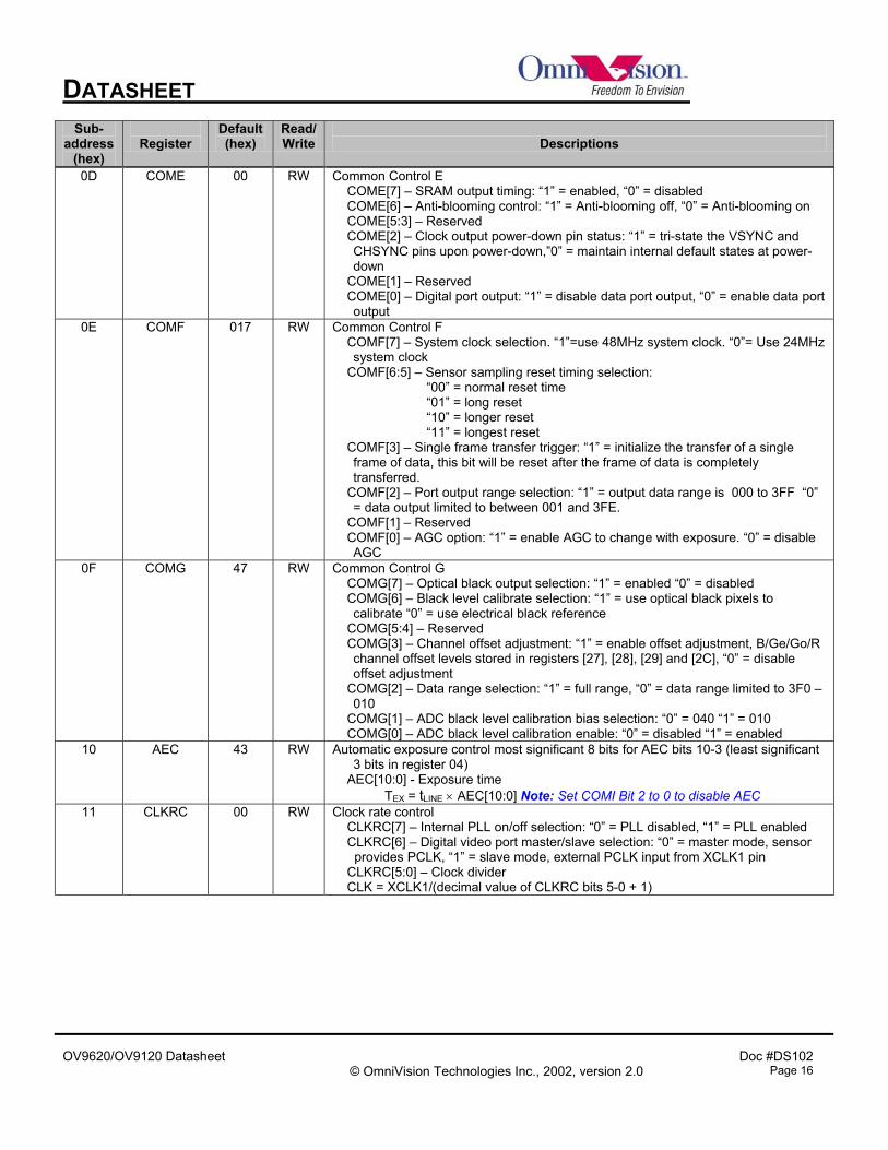
Register Set Table 13 provides a list and description of available SCCB registers contained in the OV9620/OV9120 CameraChip. The device slave addresses for the OV9620/OV9120 are 60 for write and 61 for read.
Table 13. SCCB Registers Sub-
address (hex)
Register
Default (hex)
Read/ Write
Descriptions
00 GAIN 00 RW AGC gain control GAIN[7:6] – Unimplemented. GAIN[5:0] – Gain setting. Range from 1x – 8x Note: Set COMI bit 0 to 0 to disable AGC
01 BLUE 80 RW Blue gain control MSB, 8 bits (LSB 2 bits is in register [03]). Note: This function is not available on the OV9120 CameraChip.
02 RED 80 RW Red gain control MSB, 8 bits (LSB 2 bits is in register [03]). Note: This function is not available on the OV9120 CameraChip.
03 COMA 40 RW Common Control A COMA[7:4] – AWB update threshold. COMA[3:2] – BLUE channel lower 2 bits gain control
COMA[1:0] – Red channel lower 2 bits gain control Note: This function is not available on the OV9120 CameraChip.
04 COMB 00 RW Common Control B COMB[6:5] – AWB step selection: “00” – 1023 steps, “01” – 255 steps,”10” – 511
steps, “11” – 255 steps. COMB[7:4] – AWB update speed selection: “00” – slow, “01” – slowest, “10” or “11”
– fast COMB[3] – Reserved COMB[2:0] – AEC lower 3 bits: AEC[2:0]
05 BAVG 00 RW B channel average register 06 GeAVG 00 RW G channel average register, picked G pixels in the same line with B pixels 07 GoAVG 00 RW G channel average register, picked G pixels in the same line with R pixels 08 RAVG 00 RW R channel average register 09 COMC 0C RW Common Control C
COMC[7:5] – Reserved COMC[4] – Sleep or power-down mode enable. “1” = sleep mode. “0” = normal
mode COMC[3:2] – Crystal oscillator output current; “00” = weakest “11” = strongest COMC[1:0] – Output drive current selection:”00” = weakest, “01” or “10” = double
capability, “11” = triple drive current 0A PIDH 96 R Product I.D. upper 8 bits 0B PIDL B1 R Product I.D. lower 8 bits 0C COMD 28 RW Common Control D
COMD[7] – Reserved COMD[6] – Swap MSB and LSB at the output port COMD[5:3] – Reserved COMD[2] – Snapshot mode selection: ”0” = mode1, one frame output, “1” =
mode2, two frame output COMD[1] – Sensor precharge voltage selection: “1”= selects SVDD as precharge
voltage, “0”= selects internal reference as precharge voltage. COMD[0] – Snapshot option: “0” = enables live video output after snapshot
sequence. “1” = only outputs single frame
DATASHEET
OV9620/OV9120 Datasheet Doc #DS102
© OmniVision Technologies Inc., 2002, version 2.0 Page 16
Sub-address
(hex)
Register
Default (hex)
Read/ Write
Descriptions
0D COME 00 RW Common Control E COME[7] – SRAM output timing: “1” = enabled, “0” = disabled COME[6] – Anti-blooming control: “1” = Anti-blooming off, “0” = Anti-blooming on COME[5:3] – Reserved COME[2] – Clock output power-down pin status: “1” = tri-state the VSYNC and
CHSYNC pins upon power-down,”0” = maintain internal default states at power-down
COME[1] – Reserved COME[0] – Digital port output: “1” = disable data port output, “0” = enable data port
output 0E COMF 017 RW Common Control F
COMF[7] – System clock selection. “1”=use 48MHz system clock. “0”= Use 24MHz system clock
COMF[6:5] – Sensor sampling reset timing selection: “00” = normal reset time “01” = long reset “10” = longer reset “11” = longest reset
COMF[3] – Single frame transfer trigger: “1” = initialize the transfer of a single frame of data, this bit will be reset after the frame of data is completely transferred.
COMF[2] – Port output range selection: “1” = output data range is 000 to 3FF “0” = data output limited to between 001 and 3FE.
COMF[1] – Reserved COMF[0] – AGC option: “1” = enable AGC to change with exposure. “0” = disable
AGC 0F COMG 47 RW Common Control G
COMG[7] – Optical black output selection: “1” = enabled “0” = disabled COMG[6] – Black level calibrate selection: “1” = use optical black pixels to
calibrate “0” = use electrical black reference COMG[5:4] – Reserved COMG[3] – Channel offset adjustment: “1” = enable offset adjustment, B/Ge/Go/R
channel offset levels stored in registers [27], [28], [29] and [2C], “0” = disable offset adjustment
COMG[2] – Data range selection: “1” = full range, “0” = data range limited to 3F0 – 010
COMG[1] – ADC black level calibration bias selection: “0” = 040 “1” = 010 COMG[0] – ADC black level calibration enable: “0” = disabled “1” = enabled
10 AEC 43 RW Automatic exposure control most significant 8 bits for AEC bits 10-3 (least significant 3 bits in register 04)
AEC[10:0] - Exposure time TEX = tLINE × AEC[10:0] Note: Set COMI Bit 2 to 0 to disable AEC
11 CLKRC 00 RW Clock rate control CLKRC[7] – Internal PLL on/off selection: “0” = PLL disabled, “1” = PLL enabled CLKRC[6] – Digital video port master/slave selection: “0” = master mode, sensor provides PCLK, “1” = slave mode, external PCLK input from XCLK1 pin CLKRC[5:0] – Clock divider CLK = XCLK1/(decimal value of CLKRC bits 5-0 + 1)

DATASHEET
OV9620/OV9120 Datasheet Doc #DS102
© OmniVision Technologies Inc., 2002, version 2.0 Page 17
Sub-address
(hex)
Register
Default (hex)
Read/ Write
Descriptions
12 COMH 20 RW Common control H COMH[7] – SRST, “1” initiates soft reset. All registers are set to factory default
values after which the chip resumes normal operation. COMH[6] – Resolution selection, “1” = VGA, “0” = SXGA COMH[5] – Average Luminance Value pixel counter, “1” = on, “0” = off COMH[4] – CHSYNC pin output selection: “1” =composite sync output, “0” =
output only horizontal sync COMH[3] – Master/Slave selection: “1” = slave mode, “0” = master mode COMH[2] – Window output selection: “1” = output all pixels “0” = output only
pixels defined by window registers COMH[1] – Color bar test pattern: “1” = on, “0” = off COMH[0] – ADC mode selection: “1” = 4 channel ADC, “0” = 2 channel ADC
13 COMI 07 RW Common control I COMI[7] – AEC speed selection: “0” = normal, “1” = faster AEC correction COMI[6] – AEC speed/step selection: “0” = small steps, slow, “1” = big steps, fast COMI[5] – Banding filter “0” = off, “1” = on, set minimum exposure time to 1/120s. COMI[4] – Banding filter option. Set to 0 if the main clock is 48Mhz and the PLL is
on. Set to 1 if the main clock is 24Mhz with the PLL on or the clock is 48Mhz with the PLL off.
COMI[3] – Reserved COMI[2] – Exposure control: ”0” = manual, “1” = automatic COMI[1] – AWB auto/manual control selection: ”0” = manual, “1” = auto COMI[0] – AGC auto/manual control selection: ”0” = manual, “1” = auto
14 COMJ 76 RW Common control J COMJ[7:6] – AGC gain ceiling: “11” or “10” = 8x, “01” = 4x, “00” = 2x COMJ[5] – AEC preset initial value for auto exposure mode: “1” = enabled, “0” =
disabled COMJ[4] – AWB preset initial value for auto white balance: “1” = enable, “0” =
disable COMJ[3] – Auto Banding filter: “1” = automatically disable the banding filter if light
is low. “0” = banding filter is always on/off depending on COMI[5] setting. COMJ[2] – VSYNC drop option: “1” = VSYNC is dropped if frame data is dropped.
“0” = VSYNC is always output. COMJ[1] – Frame data drop option. “1” = drop frame data if exposure not in
tolerance. In AEC mode data is normally dropped when data is out of range. “0” = disable data drop.
COMJ[0] – Freeze current Exposure and Gain values: “1” = freeze, “0” = normal 15 COMK 00 RW Common Control K
COMK[7] – CHSYNC pin output swap: “1” = HREF “0” = CHSYNC COMK[6] – HREF pin output swap: “1” = CHSYNC, “0” = HREF COMK[5] – PCLK output selection: “1” = PCLK output qualified by HREF. “0”= PLCK always output COMK[4] – PCLK edge selection: “1” = data valid on PCLK rising edge. “0” = data
valid on PCLK falling edge. COMK[3] – HREF output polarity: “1” = output negative HREF, HREF negative for
data valid. “0” = output positive HREF COMK[2] – Composite sync polarity: “1” = negative, “0” = positive COMK[1] – VSYNC polarity: “1” = negative, “0” = positive COMK[0] – HSYNC polarity:”1” = negative, “0” = positive
16 FSD 00 RW Frame slot division FSD[7] – Frame rate divider: “1” = enabled, “0” = disabled FSD[6] – Frame division: “1” = drop pre-selected number of frames, “0” = output
pre-selected frame count. Note: Frame count is set with bits 0-5 below. FSD[5:0] – Frame rate divider: [00] = select 0 frames, [01] = all frames, [02] =
select every other frame, or divide by 2, [03] – divide by 3 …, [3F] = select 1 out of every 63 frames.

DATASHEET
OV9620/OV9120 Datasheet Doc #DS102
© OmniVision Technologies Inc., 2002, version 2.0 Page 18
Sub-address
(hex)
Register
Default (hex)
Read/ Write
Descriptions
17 HREFST 1D (13
VGA)
RW Horizontal Window start most significant 8 bits, least significant bits in register [32] HS[9:0] – select beginning of horizontal window, each LSB represents two pixels.
Adjustment steps must be 2 pixels in 2-channel ADC mode and 4 pixels in 4-channel ADC mode. Note: HS [9:0] should be less than HE [9:0].
18 HREFEND BD (63
VGA)
RW Horizontal Window end most significant 8 bits, least significant bits in register [32] HE [9:0] – select the end of the horizontal window, each LSB represents two
pixels. Adjustment step must be 2 pixels in 2-channel ADC mode and 4 pixels in 4-channel ADC mode. Note: HE[9:0] should be larger than HS[9:0].
19 VSTRT 01 (02
VGA)
RW Vertical Window line start 8 MSB, LSB in register [32] VS[8:0] – selects the vertical window start, each LSB represents 4 scan lines in
SXGA or 2 lines in VGA. Note: VS[8:0] should less than VE[8:0]. 1A VEND 81
(7A VGA)
RW Vertical Window line end higher 8 bits, lowest 1 bit in register [32] VE[8:0] – selects the vertical window end, each LSB represents 4 scan lines in
SXGA and 2 lines in VGA. Note: VE[8:0] should larger than VS[7:0]. The adjustment range for vertical the window size is from [01] to [122] in SXGA and [01] to [0F4] in VGA.
1B PSHFT 00 RW Pixel shift PS[7:0] – Pixel delay count. Provides a method to fine-tune the output timing of
the pixel data relative to the HREF pulse, it physically shifts the video data output time in units of pixel clock counts. The largest delay count is “FF” and is equal to 255*PCLK.
1C MIDH 7F R Manufacture ID byte: High MIDH[7:0] – read only, always returns “7F” as manufacturer’s ID no.
1D MIDL A2 R Manufacture ID byte: Low MIDL[7:0] – read only, always returns “A2” as manufacturer’s ID no.
1E Reserve 00 RW Reserved 1F LAEC 00 RW Reserved 20 BOFF 00 RW B Channel offset adjustment, auto controlled by internal circuit if COMG[0] = 1
BOFF[7] – offset direction: “0” = add BOFF[6:0]; “1” = subtract BOFF[6:0] 21 GeOFF 80 RW Ge Channel offset adjustment, auto controlled by internal circuit if COMG[0] = 1
GeOFF[7] – offset direction: “0” = add GeOFF[6:0]; “1” = subtract GeOFF[6:0] 22 GoOFF 80 RW Go Channel offset adjustment, auto controlled by internal circuit if COMG[0] = 1
GoOFF[7] – offset direction: “0” = add GoOFF[6:0]; “1” = subtract GoOFF[6:0]. 23 ROFF 80 RW R Channel offset adjustment, auto controlled by internal circuit if COMG[0] = 1
ROFF[7] – offset direction: “0” = add ROFF[6:0]; “1” = subtract ROFF[6:0] 24 AEW A0 RW Luminance Signal High range for AEC/AGC operation
AEC/AGC value is decrease in auto modes when average luminance is greater than AEW [7:0]
25 AEB 88 RW Luminance Signal Low range for AEC/AGC operation AEC/AGC values will increase in auto mode when average luminance is less than
AEB [7:0] 26 VV F4 RW Fast mode large step range thresholds. Effective only in AEC/AGC fast mode (COMI
[7] = 1) VV [7:4] - high threshold. VV [3:0] – low threshold. AEC/AGC may change in
larger steps when luminance average is >VV [7:4] or <VV [3:0] 27 BBIAS 80 RW B Channel offset manual adjustment value, effect only when COMG[3] = 1
BBIAS[7] – offset direction: “0” = add BBIAS[6:0]; “1” = subtract BBIAS[6:0] 28 GeBIAS 80 RW Ge Channel offset manual adjustment value, effect only when COMG[3] = 1
GeBIAS [7] – offset direction: “0” = add GeBIAS[6:0]; “1” = subtract GeBIAS [6:0] 29 GoBIAS 80 RW Go Channel offset manual adjustment value, effect only when COMG[3] = 1
GoBIAS[7] – offset direction: “0” = add GoBIAS [6:0]; “1” = subtract GoBIAS [6:0].

DATASHEET
OV9620/OV9120 Datasheet Doc #DS102
© OmniVision Technologies Inc., 2002, version 2.0 Page 19
Sub-address
(hex)
Register
Default (hex)
Read/ Write
Descriptions
2A COML 00 RW Common control L COML[7] – Line interval adjustment : “1” = enabled, “0” = disabled. Interval
adjustment value in COM [6:5] and FRARL [7:0]. COML[6:5] – Line interval adjust value most significant 2 bits COML[4] – AGC preset initial value for auto gain control: “1” = enabled, “0” =
disabled: Note: preset in register 00. COML[3:2] – HSYNC timing end point adjustment MSB 2 bits COML[1:0] – HSYNC timing start point adjustment MSB 2 bits
2B FRARL 00 RW Line interval adjustment value LSB 8 bits The frame rate will be adjusted by changing the line interval. Each LSB will add
2/1520 Tframe in SXGA mode and 2/800 Tframe in VGA mode to the frame period. 2C RBIAS 80 RW R Channel offset manual adjustment value, effective only when COMG[3] = 1
RBIAS[7] – offset direction: “0” = add RBIAS[6:0]; “1” = subtract RBIAS[6:0] 2D ADDVSL 00 RW VSYNC Pulse width LSB 8 bits
ADDVSL[7:0] – line periods added to VSYNC width. Default VSYNC output width is 4 * tline. Each LSB count will add 1 * tline to the VSYNC active period.
2E ADDVSH 00 RW VSYNC Pulse width MSB 8 bits ADDVSH[7:0] – line periods added to VSYNC width. Default VSYNC output is 4 *
tline. Each MSB count will add 256 * tline in VSYNC period 2F YAVG 00 RW Luminance average register
This register will auto update when COMH [5] = 1; Average Luminance is calculated from R/Ge/Go/R channel average, it is equal to (Blue Avg [7:0] + GeAVG[7:0] + GoAVG[7:0] + RAVG[7:0])/4
30 HSDY 08 RW HSYNC position and width start point LSB 8 bits This register and COML[1:0] define HSYNC start position, each LSB will shift
HSYNC start point by 1 pixel period. 31 HEDY 30 RW HSYNC position and width end lower 8 bits
This register and COML[3:2] define HSYNC end position, each LSB will shift HSYNC end by 1 pixel period.
32 COMM 0A (0F in VGA)
RW Common control M COMM[7] – Pixel blanking period; “1” = set pixel blanking to 040 to each side of
HREF. COMM[6] – Blank pixel value setting: “1” = set pixel blanking to 010 periods to
each side of HREF. Default pixel blanking is 0 COMM[5] – Vertical window end position LSB COMM[4] – Vertical window start position LSB COMM[3:2] – Horizontal window end position LSBs COMM[1:0] – Horizontal window start position LSBs
33 CHLF 28 RW Current control CHLF[7:6] – Sensor current control,”00”= minimum, “11”= maximum CHLF[5] – Sensor current range control: “0”= CHLF[7:6] current control at normal
range, “1”= CHLF[7:6] current at half range CHLF[4] – Sensor Current double on/off: “0”= normal, “1”= double current CHLF[3] – Sensor buffer current control: “0”= normal, “1”= current half CHLF[2] – Column buffer current control: “0”= normal, “1”= current half CHLF[1] – Analog DSP current control: “0”= normal, “1”= current half CHLF[0] – ADC current control: “0”= normal, “1”= current half
34 VGAP 1B RW Reserved 35 VBLM 90 RW Reference voltage control
VBLM[7:5] – Column high reference control: “1xx”= column high reference connect to VDD, “000”= lowest voltage “011”= highest voltage
VBLM[4:2] – Column low reference control: “1xx”= column low reference connect to GND, “000”= lowest “011”= highest
VBLM[1:0] – Anti-blooming voltage control: “00”= lowest voltage, “11”= highest voltage, these 2 bits enabled/disabled by COME[6].

DATASHEET
OV9620/OV9120 Datasheet Doc #DS102
© OmniVision Technologies Inc., 2002, version 2.0 Page 20
Sub-address
(hex)
Register
Default (hex)
Read/ Write
Descriptions
36 VCHG 17 RW Sensor precharge voltage control VCHG[7] – reserved VCHG[6:4] – Sensor precharge voltage control: “000”= lowest voltage “111”=
highest voltage. VCHG[3:0] – Sensor array common reference control: “000”= lowest voltage
“111”= highest voltage 37 ADC 04 RW ADC reference control
ADC[7:4] – reserved ADC[3] – ADC input signal range: “1”= input signal x0.7, “0”= input signal x1. ADC[2:0] – ADC range control. “000”= Minimum, “111”= Maximum.
38 ACOM 12 RW Analog Common Control ACOM[7] – Analog gain control: “1”= Gain increase 1.5x, “0”= Normal ACOM[6] – Analog black level calibration control: “0”= Analog BLC on, “1”= Analog
BLC off. ACOM[5:0] – reserved.
38 ACOM 12 RW Analog Common Control ACOM[7] – Analog gain control: “1”= Gain increase 1.5x, “0”= Normal ACOM[6] – Analog black level calibration control: “0”= Analog BLC on, “1”=
Analog BLC off. ACOM[5:0] – reserved.

DATASHEET
OV9620/OV9120 Datasheet Doc #DS102
© OmniVision Technologies Inc., 2002, version 2.0 Page 21
OV9620/OV9120 Package Information
Figure 23. OV9620/9120 Package Diagram
30
19 6
43
48
+0.0100.060 -0.005
0.085 ±0.010
0.020 ±0.0020.030
±0.002
0.065 ±0.007
Bottom View
Top View
Side View
18 7
31 42
0.440 ±0.005
R 0.007548 PLCS
R 0.00754 CORNERS
0.020 ±0.008TYP
0.040 ±0.007TYP
0.040 ±0.003
43
6 19
30
48
42 310.350 SQ ±0.0050.430 SQ ±0.005
+0.0120.560 SQ -0.005
0.003 0.003
0.002
7 18
43
1
6
7 18
19
303142
0.002 TYP
0.006 MAX
0.03
6 M
IN

DATASHEET
OV9620/OV9120 Datasheet Doc #DS102
© OmniVision Technologies Inc., 2002, version 2.0 Page 22
Die shift (x,y)=0.15mm (6mils) max.Die tilt=2 degrees max.Die rotation=3 degrees max.
Package Center(0, 0)
SensorArray
Package
A
B
C
D
Array Center
(0.62 mil, -10.69 mil)(15.7µm, -271.6µm)
A=1378.03µm (54.25mils)
D=524.5µm (20.65mils)C=834.77µm (32.86mils)B=493.1µm (19.41mils)
Dimensions
Positional Tolerances
Pin 1
1
Die
Figure 24. OV9620/9120 Sensor array center location
Note: Picture is for reference only, not to scale. OmniVision Technologies, Inc. reserves the right to make changes without further notice to any product herein to improve reliability, function, or design. OmniVision Technologies, Inc. does not assume any liability arising out of the application or use of any product or circuit described herein; neither does it convey any license under its patent rights nor the rights of others. No part of this publication may be copied or reproduced, in any form, without the prior written consent of OmniVision Technologies, Inc.
IMPORTANT: Most optical systems invert and mirror the image so the chip is usually mounted on the board with pin 1 (SVDD) down as shown.
DATASHEET
OV9620/OV9120 Datasheet Doc #DS102
© OmniVision Technologies Inc., 2002, version 2.0 Page 23
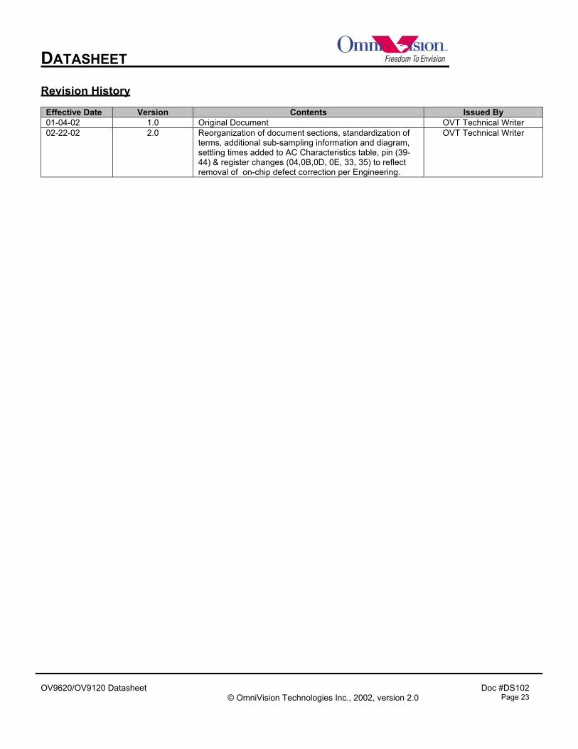
Revision History
Effective Date Version Contents Issued By 01-04-02 1.0 Original Document OVT Technical Writer 02-22-02 2.0 Reorganization of document sections, standardization of
terms, additional sub-sampling information and diagram, settling times added to AC Characteristics table, pin (39-44) & register changes (04,0B,0D, 0E, 33, 35) to reflect removal of on-chip defect correction per Engineering.
OVT Technical Writer