Overview of system-level protection in class-D audio ... · Overview of system-level protection in...
10
Overview of system-level protection in class-D audio amplifiers Mark Toth Marketing manager, Mid-Power Audio Amplifier Products Texas Instruments Jeff Kohnle Applications manager, Mid-Power Audio Amplifier Products Texas Instruments Morgan Lollar Applications manager, Low-Power Audio Amplifier Products Texas Instruments Chuck Smyth Applications engineer, Low-Power Audio Amplifier Products Texas Instruments
Transcript of Overview of system-level protection in class-D audio ... · Overview of system-level protection in...

Overview of system-level protection in class-D audio amplifiers
Mark TothMarketing manager, Mid-Power Audio Amplifier Products Texas Instruments
Jeff KohnleApplications manager,Mid-Power Audio Amplifier Products Texas Instruments
Morgan LollarApplications manager, Low-Power Audio Amplifier Products Texas Instruments
Chuck SmythApplications engineer,Low-Power Audio Amplifier Products Texas Instruments
Overview of system-level protection in class-D audio amplifiers 2 December 2017
Class-D audio amplifiers with integrated system protection features help engineers create robust and reliable audio designs.
The class-D audio amplifier topology is designed to reduce power consumption
and thermal dissipation compared to traditional linear audio amplifier
topologies such as class A, class B and class AB. When class-D amplifier
technology was initially developed, designers mainly focused on improving
these two specifications.
As class-D amplifier technology matured, class-D
products integrated more and more features beyond
improved efficiency and thermal performance.
One of the key areas addressed is improved
system-level reliability, which helps designers ensure
that a system operates reliably in its intended
application. A typical audio system has several key
items that need protection to help ensure reliable
system function:
• The audio amplifier integrated circuit (IC) itself
needs protection from potentially damaging
temperature, voltage, current and input signals.
• The system power supply needs protection from
load currents and voltages that exceed the power-
supply capability and can cause unintended
operation or damage.
• The system needs electromagnetic compatibility
(EMC) protection that avoids interference with
other devices and allows successful product
compliance testing.
• Finally, the system transducer (or speaker) needs
protection from electrical and physical damage
caused by various stresses.
This paper provides a high-level overview of a
number of system-level protection features found
in class-D audio amplifiers, and how they help to
ensure stable operation.
Overcurrent protection Overcurrent protection (OCP) detects when a
predetermined output current threshold has been
exceeded, and shuts the amplifier down to help
protect it from damage. The electrical capability of
the internal circuits to deliver current without damage
determines the output current limits of different
class-D amplifiers. Upon a detected shutdown, the
amplifier drives a digital output signal to the host
processor to communicate that an overcurrent fault
has occurred.
Examples of some overcurrent conditions are
attributed to shorted wiring, printed circuit board
(PCB) traces, component faults or damaged
speakers. By limiting the output current of an
amplifier to a level that won’t damage it, OCP can
help protect both the amplifier and system power
supply from certain, reliability-based, stress-induced
damage. OCP can also protect speakers from
overcurrent, as well as provide a protective element
to minimize risks of system-related overheating.
External current-protection circuits add cost and
complexity, and are typically less robust than
Overview of system-level protection in class-D audio amplifiers 3 December 2017
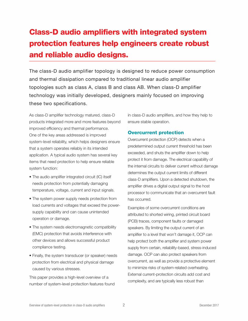
integrated OCP. Figure 1 shows an example timing
diagram of OCP in a class-D amplifier.
Overtemperature protection Overtemperature protection (OTP) detects when
the temperature of the amplifier exceeds a specified
level resulting in the amplifier shutting down to help
protect itself from damage. The individual amplifier
characteristics help establish an appropriate
temperature limitation. Upon shutdown, the amplifier
drives a digital output signal to the host processor
to communicate that an overtemperature fault has
occurred.
OTP events can occur due to abnormally high
ambient temperatures, unexpected audio signals or
a variety of unanticipated system faults. OTP helps
to protect class-D amplifiers from overheating and
potentially causing further system-related issues.
Some class-D amplifier devices also have
overtemperature warning (OTW) functionality,
which warns the system host when the amplifier
temperature nears operational limits so that the host
can take action, such as reducing gain or shutting
down a channel, to decrease system temperature.
AM interference avoidance Switching amplifiers, including class-D, can produce
AM interference by emitting radio energy emissions
near the digital amplifier’s switching rate as well as
the harmonics of that switching rate, meaning that
the fundamental frequency and its second harmonic
straddle the AM radio band. This can be an issue
when the digital amplifier is located by the AM radio
(as in an automotive infotainment module or an
integrated home audio system).
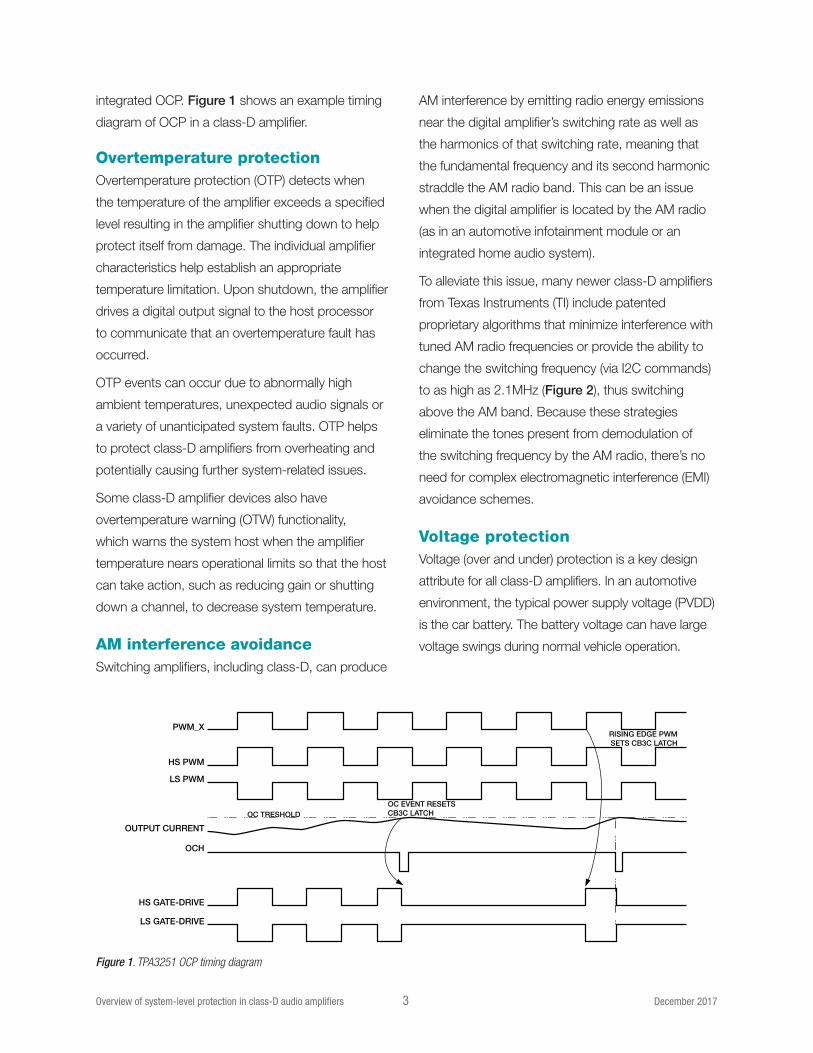
To alleviate this issue, many newer class-D amplifiers
from Texas Instruments (TI) include patented
proprietary algorithms that minimize interference with
tuned AM radio frequencies or provide the ability to
change the switching frequency (via I2C commands)
to as high as 2.1MHz (Figure 2), thus switching
above the AM band. Because these strategies
eliminate the tones present from demodulation of
the switching frequency by the AM radio, there’s no
need for complex electromagnetic interference (EMI)
avoidance schemes.
Voltage protection Voltage (over and under) protection is a key design
attribute for all class-D amplifiers. In an automotive
environment, the typical power supply voltage (PVDD)
is the car battery. The battery voltage can have large
voltage swings during normal vehicle operation.
PWM_X
HS PWM
RISING EDGE PWMSETS CB3C LATCH
OC EVENT RESETSCB3C LATCHOC TRESHOLD
LS PWM
OUTPUT CURRENT
OCH
HS GATE-DRIVE
LS GATE-DRIVE
Figure 1. TPA3251 OCP timing diagram
Overview of system-level protection in class-D audio amplifiers 4 December 2017
There’s also the possibility of an unusual event such
as a load dump.
TI automotive devices help protect against
overvoltage on the PVDD pin for up to 50V load-
dump spikes. Undervoltage protection also exists
on the PVDD, analog supply voltage (AVDD), digital
supply voltage (DVDD) and charge-pump supply
voltage (CPVDD) pins. If a CP undervoltage condition
occurs, the AVDD voltage turns off and an AVDD
undervoltage fault occurs. In this case, both CP
and AVDD undervoltage bits will be set and the real
undervoltage fault is CP.
TI’s general purpose class-D devices contain
protection circuit features designed to make system
design more efficient as well as to help protect against
permanent failures, including short circuits, overload,
and over- and undervoltage. Table 1 lists a typical
fault reporting schedule.
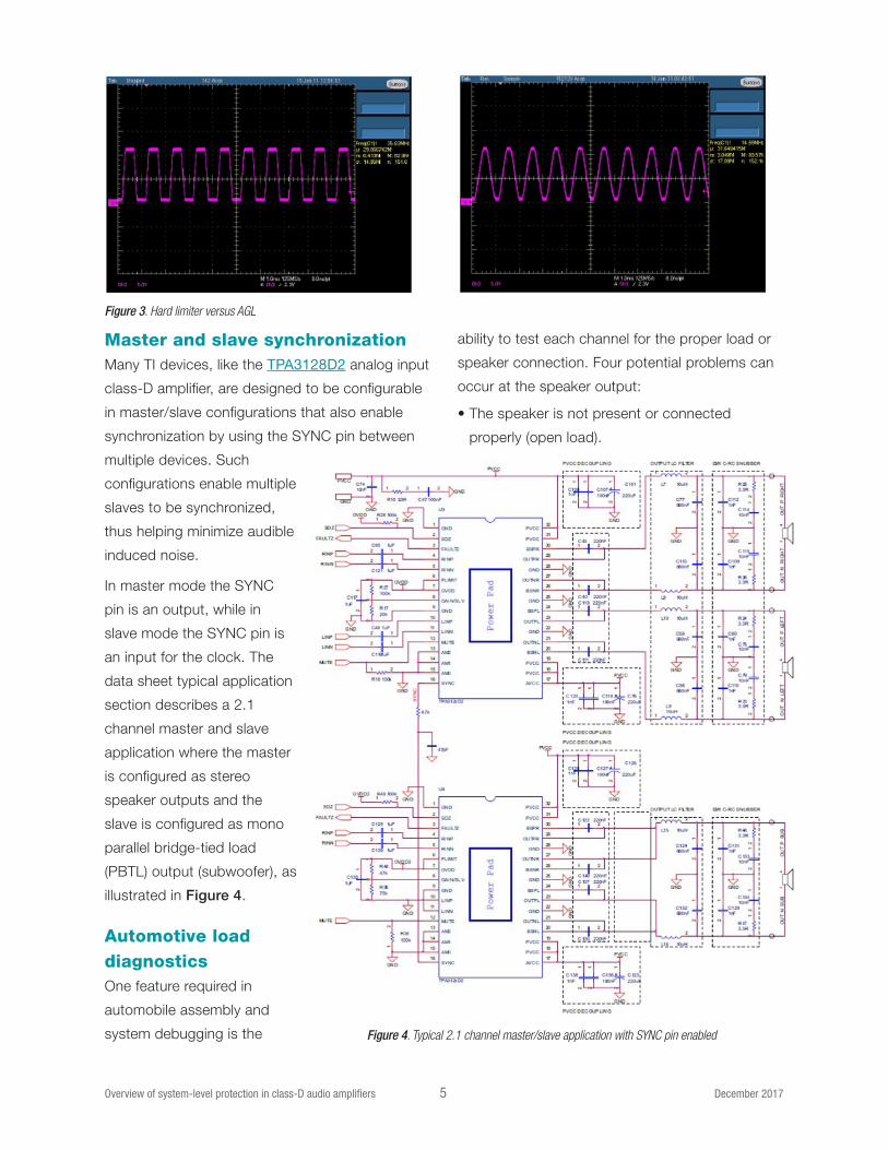
Automatic gain limit versus a hard limiter
Automatic gain limit (AGL) is an enhanced dynamic
range compression (DRC) function used in many
TI class-D audio amplifiers, which essentially
compresses the output power without clipping
the output waveforms. It has a feedback topology
as opposed to the traditional DRC feed-forward
topology that enables the AGL algorithm to
immediately compress the incoming signal when it
is over the threshold in a short amount of time (i.e. a
very small attack time).
To implement AGL, simply adjust the desired level
for each of its component parameters:
• The threshold specifies the application of AGL
(compression).
• The softening filter takes out the harmonics during
hard compression.
• The attack and release times specify how quickly
compression turns on and off, respectively.
By setting these appropriately, you will find that the
output waveforms do not clip as much as under
other schemes.
An alternative scheme known as a hard limiter
restricts the power by clamping the output to pre-
set highs and lows (Vpk-pk) producing a clipped
waveform which results in much higher distortion
(Figure 3).
dB
µV/m
Frequency (kHz)535 1705 2100
AM band
2.1 MHz PWMswitching frequency
Figure 2. 2.1MHz PWM switching frequency
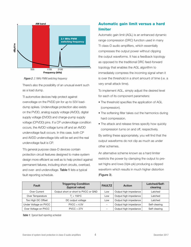
Table 1. Typical fault reporting schedule
FaultTriggering Condition
(typical value)FAULTZ Action
Latched/Self-clearing
Over Current Output short or short to PVCC or GND Low Output high impedance Latched
Over Temperature Tj > 150oC Low Output high impedance Latched
Too High DC Offset DC output voltage Low Output high impedance Latched
Under Voltage on PVCC PVCC < 4.5V – Output high impedance Self-clearing
Over Voltage on PVCC PVCC > 27V – Output high impedance Self-clearing
Overview of system-level protection in class-D audio amplifiers 5 December 2017
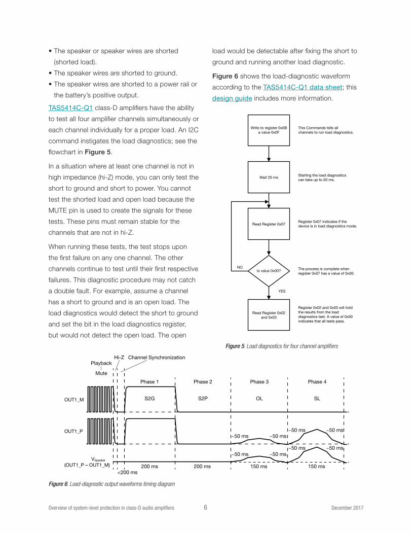
Master and slave synchronization Many TI devices, like the TPA3128D2 analog input
class-D amplifier, are designed to be configurable
in master/slave configurations that also enable
synchronization by using the SYNC pin between
multiple devices. Such
configurations enable multiple
slaves to be synchronized,
thus helping minimize audible
induced noise.
In master mode the SYNC
pin is an output, while in
slave mode the SYNC pin is
an input for the clock. The
data sheet typical application
section describes a 2.1
channel master and slave
application where the master
is configured as stereo
speaker outputs and the
slave is configured as mono
parallel bridge-tied load
(PBTL) output (subwoofer), as
illustrated in Figure 4.
Automotive load diagnostics One feature required in
automobile assembly and
system debugging is the
ability to test each channel for the proper load or
speaker connection. Four potential problems can
occur at the speaker output:
• The speaker is not present or connected
properly (open load).
Figure 4. Typical 2.1 channel master/slave application with SYNC pin enabled
Figure 3. Hard limiter versus AGL
Overview of system-level protection in class-D audio amplifiers 6 December 2017
• The speaker or speaker wires are shorted
(shorted load).
• The speaker wires are shorted to ground.
• The speaker wires are shorted to a power rail or
the battery’s positive output.
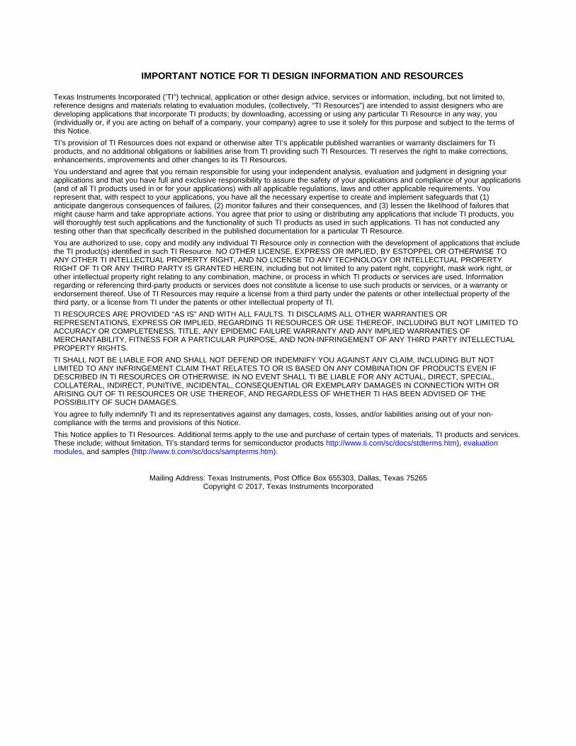
TAS5414C-Q1 class-D amplifiers have the ability
to test all four amplifier channels simultaneously or
each channel individually for a proper load. An I2C
command instigates the load diagnostics; see the
flowchart in Figure 5.
In a situation where at least one channel is not in
high impedance (hi-Z) mode, you can only test the
short to ground and short to power. You cannot
test the shorted load and open load because the
MUTE pin is used to create the signals for these
tests. These pins must remain stable for the
channels that are not in hi-Z.
When running these tests, the test stops upon
the first failure on any one channel. The other
channels continue to test until their first respective
failures. This diagnostic procedure may not catch
a double fault. For example, assume a channel
has a short to ground and is an open load. The
load diagnostics would detect the short to ground
and set the bit in the load diagnostics register,
but would not detect the open load. The open
load would be detectable after fixing the short to
ground and running another load diagnostic.
Figure 6 shows the load-diagnostic waveform
according to the TAS5414C-Q1 data sheet; this
design guide includes more information.
This Commands tells all channels to run load diagnostics.
Write to register 0x0B a value 0x0F
Starting the load diagnostics can take up to 20 ms.
Register 0x07 indicates if the device is in load diagnostics mode.
Register 0x02 and 0x03 will hold the results from the load diagnostics test. A value of 0x00 indicates that all tests pass.
The process is complete when register 0x07 has a value of 0x00.
Wait 20 ms
Read Register 0x07
Is value 0x00?
Read Register 0x02and 0x03
NO
YES
Figure 5. Load diagnostics for four channel amplifiers
Figure 6. Load-diagnostic output waveforms timing diagram
OUT1_M
OUT1_P
(OUT1_P – OUT1_M)VSpeaker
<200 ms200 ms
S2G
Phase 1
Channel SynchronizationHi-ZPlayback
Mute
S2P
Phase 2
200 ms
OL
Phase 3
150 ms
~50 ms ~50 ms
~50 ms ~50 ms
~50 ms ~50 ms
~50 ms ~50 ms
SL
Phase 4
150 ms

Overview of system-level protection in class-D audio amplifiers 7 December 2017
Note that we presented these waveforms in this
form to emphasize how the device applies the
load diagnostic signal. The actual amplitude of the
applied signals in phase 3 (open load) and phase
4 (shorted load) are highly load-dependent and
may have greatly decreased amplitude compared
to those shown in Figure 6 when a load is
properly connected.
DC detection One of the more common fault protections is DC
detection, which is designed to minimize risk of
damage to the output stage in case of a short
circuit or some other similar fault. This protection
scheme also helps prevent any rail voltage
present from connecting directly to the speaker.
The TI amplifier’s circuit detects a DC offset at
the output of the amplifier continuously during
normal operation. If the DC offset reaches the level
defined in the I2C registers for the specified time
period for a particular device, the circuit triggers
a channel shutdown. The I2C conducts the
disabling and enabling of the shutdown function.
If enabled, the triggered channel shuts down,
while the other channels remain in play mode with
the FAULT pin asserted.
Clock error handling TI’s digital input amplifiers typically require two or
three clock input signals, such as master clock
(MCLK), serial clock (SCLK) and left-right clock
(LRCLK). One other feature included in the suite
of error-handling and protection features of TI
amplifiers is related to the detection of clock errors
(CLKE). One or more of the following errors has to
occur for a clock error to register:
• Nonsupported MCLK to LRCLK and/or SCLK to
LRCLK ratio.
• Nonsupported MCLK or LRCLK rate.
• Either MCLK, SCLK or LRCLK has stopped.
The speaker fault (SPK_FAULT) pin and
appropriate error status register in the I²C
control port report the status of clock errors.
The clock-error-handling behavior of the device
is characterized as “nonlatching,” which means
that once the fault is clear, the device resumes
normal operation (such as audio playback). The
general clock error mechanism is that once
an error is detected, the SPK_FAULT pin will
pull low. Once the error has cleared and the
clock returns to a valid state, normal operation
resumes automatically.
Excursion control Excursion is the distance which a speaker
diaphragm moves in and out from its resting
position. It needs to be controlled to avoid the
diaphragm from traveling past its excursion
limit, which can lead to damage in the speaker.
Amplifiers control the excursion in real time by
monitoring it via current and voltage (IV) sense
feedback or in a feed-forward model created
for the speaker, shown in Figure 7. Traditional
Figure 7. Comparison of audio between amplifiers with and without IV sense

Overview of system-level protection in class-D audio amplifiers 8 December 2017
amplifiers attenuate the entire signal as a means
for control.
The ability to control excursion enables real-time
protection to drive peaks to the excursion limit
without damaging the speaker, which results in
increased sound pressure level.
Voice coil temperature Voice coil temperature is the heat generated
by the electrical power, delivered by the audio
amplifier to the speaker coil while playing audio. If
not monitored (especially in small speakers), the
coil can heat up past the thermal limit and cause
damage to the speaker and surrounding materials.
Amplifiers control the temperature in real time by
monitoring it via IV sense feedback or in a feed-
forward model created for the speaker. Figure
8 shows an example of estimated voice coil
temperature, and how TI’s advanced algorithms
can control this temperature within its required
operating limits.
Speaker protection Speaker protection is an algorithm used in smart
amplifiers to monitor the speaker excursion and
voice coil temperature to ensure reliable operation.
The algorithm uses IV sense information to update
the speaker model in real time, which enables
the amplifier to reliably and effectively drive the
speaker with higher energy peaks compared to a
standard class-D audio amplifier, while keeping the
speaker under maximum temperature (Tmax) and
maximum excursion (Xmax) operating limits.
Figure 9 illustrates where the speaker protection
resides in the smart amplifier signal chain,
including the feedback path at the speaker nodes.
Figure 9. Example of a smart amplifier system
Figure 8. Voice coil temperature monitoring in TI PurePath™ Console 3 software
Host TAS2557
Feedback Path VSENSE
OUTDSP
SpeakerClass
DPre-processingI2C
PBEInputGain
EQ DRC
Smart Amp Protection• Excursion Protection• Thermal Protection• Anti-clipper

Smart bass Microspeakers are commonly used in compact
mobile devices and typically have limited low-
frequency bandwidth, resulting in poor bass
performance. Smart bass (also known as
psychoacoustic bass) enhances the perceived low-
end response of the speaker without introducing
actual additional excursion at low frequencies –
where microspeakers often already have limited
excursion headroom.
Conclusion In today’s advanced audio system designs, class-D
audio amplifiers with integrated system protection
features can help system designers create robust
and reliable products that end customers want to
buy. For more information about these features,
check out TI’s portfolio of audio devices.
Important Notice: The products and services of Texas Instruments Incorporated and its subsidiaries described herein are sold subject to TI’s standard terms and conditions of sale. Customers are advised to obtain the most current and complete information about TI products and services before placing orders. TI assumes no liability for applications assistance, customer’s applications or product designs, software performance, or infringement of patents. The publication of information regarding any other company’s products or services does not constitute TI’s approval, warranty or endorsement thereof.
© 2017 Texas Instruments Incorporated SLYY125
The platform bar is a trademark of Texas Instruments.All other trademarks are the property of their respective owners.
Transducer Bandwidth Limitation
Perceived Level
Fundamental HarmonicsFrequency
Mag
nitu
de
Figure 10. Bandwidth limitations of microspeakers and how smart bass can improve perceived bass
IMPORTANT NOTICE FOR TI DESIGN INFORMATION AND RESOURCES
Texas Instruments Incorporated (‘TI”) technical, application or other design advice, services or information, including, but not limited to,reference designs and materials relating to evaluation modules, (collectively, “TI Resources”) are intended to assist designers who aredeveloping applications that incorporate TI products; by downloading, accessing or using any particular TI Resource in any way, you(individually or, if you are acting on behalf of a company, your company) agree to use it solely for this purpose and subject to the terms ofthis Notice.TI’s provision of TI Resources does not expand or otherwise alter TI’s applicable published warranties or warranty disclaimers for TIproducts, and no additional obligations or liabilities arise from TI providing such TI Resources. TI reserves the right to make corrections,enhancements, improvements and other changes to its TI Resources.You understand and agree that you remain responsible for using your independent analysis, evaluation and judgment in designing yourapplications and that you have full and exclusive responsibility to assure the safety of your applications and compliance of your applications(and of all TI products used in or for your applications) with all applicable regulations, laws and other applicable requirements. Yourepresent that, with respect to your applications, you have all the necessary expertise to create and implement safeguards that (1)anticipate dangerous consequences of failures, (2) monitor failures and their consequences, and (3) lessen the likelihood of failures thatmight cause harm and take appropriate actions. You agree that prior to using or distributing any applications that include TI products, youwill thoroughly test such applications and the functionality of such TI products as used in such applications. TI has not conducted anytesting other than that specifically described in the published documentation for a particular TI Resource.You are authorized to use, copy and modify any individual TI Resource only in connection with the development of applications that includethe TI product(s) identified in such TI Resource. NO OTHER LICENSE, EXPRESS OR IMPLIED, BY ESTOPPEL OR OTHERWISE TOANY OTHER TI INTELLECTUAL PROPERTY RIGHT, AND NO LICENSE TO ANY TECHNOLOGY OR INTELLECTUAL PROPERTYRIGHT OF TI OR ANY THIRD PARTY IS GRANTED HEREIN, including but not limited to any patent right, copyright, mask work right, orother intellectual property right relating to any combination, machine, or process in which TI products or services are used. Informationregarding or referencing third-party products or services does not constitute a license to use such products or services, or a warranty orendorsement thereof. Use of TI Resources may require a license from a third party under the patents or other intellectual property of thethird party, or a license from TI under the patents or other intellectual property of TI.TI RESOURCES ARE PROVIDED “AS IS” AND WITH ALL FAULTS. TI DISCLAIMS ALL OTHER WARRANTIES ORREPRESENTATIONS, EXPRESS OR IMPLIED, REGARDING TI RESOURCES OR USE THEREOF, INCLUDING BUT NOT LIMITED TOACCURACY OR COMPLETENESS, TITLE, ANY EPIDEMIC FAILURE WARRANTY AND ANY IMPLIED WARRANTIES OFMERCHANTABILITY, FITNESS FOR A PARTICULAR PURPOSE, AND NON-INFRINGEMENT OF ANY THIRD PARTY INTELLECTUALPROPERTY RIGHTS.TI SHALL NOT BE LIABLE FOR AND SHALL NOT DEFEND OR INDEMNIFY YOU AGAINST ANY CLAIM, INCLUDING BUT NOTLIMITED TO ANY INFRINGEMENT CLAIM THAT RELATES TO OR IS BASED ON ANY COMBINATION OF PRODUCTS EVEN IFDESCRIBED IN TI RESOURCES OR OTHERWISE. IN NO EVENT SHALL TI BE LIABLE FOR ANY ACTUAL, DIRECT, SPECIAL,COLLATERAL, INDIRECT, PUNITIVE, INCIDENTAL, CONSEQUENTIAL OR EXEMPLARY DAMAGES IN CONNECTION WITH ORARISING OUT OF TI RESOURCES OR USE THEREOF, AND REGARDLESS OF WHETHER TI HAS BEEN ADVISED OF THEPOSSIBILITY OF SUCH DAMAGES.You agree to fully indemnify TI and its representatives against any damages, costs, losses, and/or liabilities arising out of your non-compliance with the terms and provisions of this Notice.This Notice applies to TI Resources. Additional terms apply to the use and purchase of certain types of materials, TI products and services.These include; without limitation, TI’s standard terms for semiconductor products http://www.ti.com/sc/docs/stdterms.htm), evaluationmodules, and samples (http://www.ti.com/sc/docs/sampterms.htm).
Mailing Address: Texas Instruments, Post Office Box 655303, Dallas, Texas 75265Copyright © 2017, Texas Instruments Incorporated