
Four-wave mixing and nonlinear parameter measurement in a ...

IntroductionUntil recently, power amplifier design for wireless communication has been focused on specified fractional bandwidths of 5% or less, primarily due to the utilization of a single amplifier per defined spectrum allocation. With both a focus on reducing power consumption and cost, coupled with emerging applications like 4G and WiMax utilizing new spectrum allocations, amplifier designs are simultaneously attempting to address wider bandwidth operation to reduce parts count and increase efficiency. These factors influencing the development of power amplifiers has caused designers to work with newer technologies, such as GaN HFETs, to achieve higher power and higher efficiency amplifiers across wider bands of operation.
Optimizing the performance of a power amplifier, PA, requires an understanding of the performance in it’s nonlinear region. As the natural distortion of the device itself produces harmonically related products, the realization of a highly efficient PA is fundamentally coupled to the precise control of the fundamental and harmonic impedances that are presented to the device. Traditional measurement systems enable systematic load-pull sweeps at the fundamental frequency with typical measurements including device measurements at several hundred impedance points. Extending the same approach to harmonic load pull measurements would require the measurement of all the impedance points of the fundamental and harmonic impedances at all possible combinations.
Overcoming Nonlinear Measurement ChallengesApplication Note
Application Note
www.tektronix.com/rf2
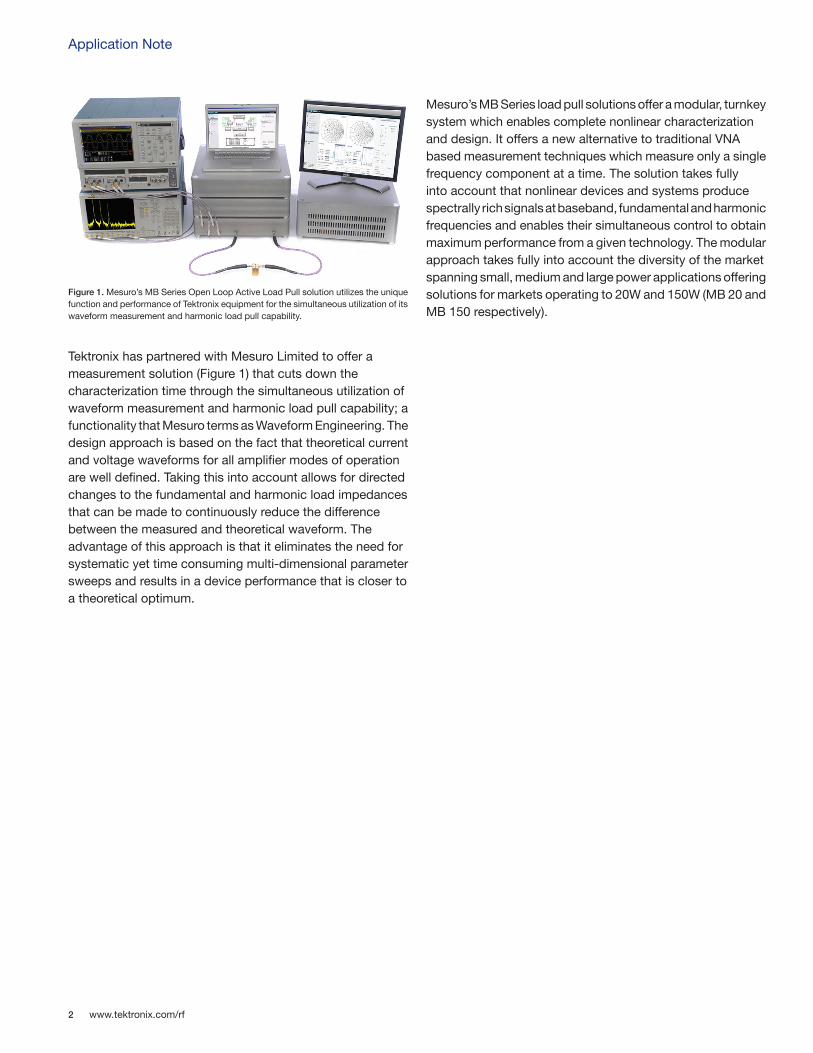
Tektronix has partnered with Mesuro Limited to offer a measurement solution (Figure 1) that cuts down the characterization time through the simultaneous utilization of waveform measurement and harmonic load pull capability; a functionality that Mesuro terms as Waveform Engineering. The design approach is based on the fact that theoretical current and voltage waveforms for all amplifier modes of operation are well defined. Taking this into account allows for directed changes to the fundamental and harmonic load impedances that can be made to continuously reduce the difference between the measured and theoretical waveform. The advantage of this approach is that it eliminates the need for systematic yet time consuming multi-dimensional parameter sweeps and results in a device performance that is closer to a theoretical optimum.
Mesuro’s MB Series load pull solutions offer a modular, turnkey system which enables complete nonlinear characterization and design. It offers a new alternative to traditional VNA based measurement techniques which measure only a single frequency component at a time. The solution takes fully into account that nonlinear devices and systems produce spectrally rich signals at baseband, fundamental and harmonic frequencies and enables their simultaneous control to obtain maximum performance from a given technology. The modular approach takes fully into account the diversity of the market spanning small, medium and large power applications offering solutions for markets operating to 20W and 150W (MB 20 and MB 150 respectively).
Figure 1. Mesuro’s MB Series Open Loop Active Load Pull solution utilizes the unique function and performance of Tektronix equipment for the simultaneous utilization of its waveform measurement and harmonic load pull capability.
www.tektronix.com/rf 3
Overcoming Nonlinear Measurement Challenges
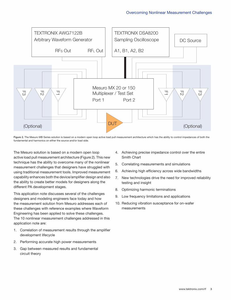
The Mesuro solution is based on a modern open loop active load pull measurement architecture (Figure 2). This new technique has the ability to overcome many of the nonlinear measurement challenges that designers have struggled with using traditional measurement tools. Improved measurement capability enhances both the device/amplifier design and also the ability to create better models for designers along the different PA development stages.
This application note discusses several of the challenges designers and modeling engineers face today and how the measurement solution from Mesuro addresses each of these challenges with reference examples where Waveform Engineering has been applied to solve these challenges. The 10 nonlinear measurement challenges addressed in this application note are:
1. Correlation of measurement results through the amplifier development lifecycle
2. Performing accurate high power measurements
3. Gap between measured results and fundamental circuit theory
4. Achieving precise impedance control over the entire Smith Chart
5. Correlating measurements and simulations
6. Achieving high efficiency across wide bandwidths
7. New technologies drive the need for improved reliability testing and insight
8. Optimizing harmonic terminations
9. Low frequency limitations and applications
10. Reducing vibration susceptance for on-wafer measurements
Figure 2. The Mesuro MB Series solution is based on a modern open loop active load pull measurement architecture which has the ability to control impedances of both the fundamental and harmonics on either the source and/or load side.
(Optional) DUT
TEXTRONIX AWG7122BArbitrary Waveform Generator
RFS Out RFL Out
TEXTRONIX DSA8200Sampling Oscilloscope
A1, B1, A2, B2
DC Source
F3 F2 F1
(Optional)
F3F2F1
Mesuro MX 20 or 150Multiplexer / Test SetPort 1 Port 2
Application Note
www.tektronix.com/rf4
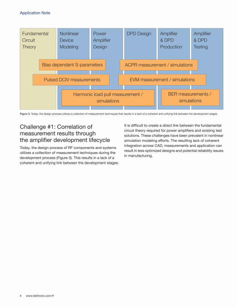
Figure 3. Today, the design process utilizes a collection of measurement techniques that results in a lack of a coherent and unifying link between the development stages.
NonlinearDeviceModeling
PowerAmplifierDesign
DPD Design Amplifier& DPDProduction
Amplifier& DPDTesting
FundamentalCircuitTheory
Bias dependent S-parameters ACPR measurement / simulations
EVM measurement / simulations
BER measurements / simulations
Harmonic load pull measurement /simulations
Pulsed DCIV measurements
Challenge #1: Correlation of measurement results through the amplifier development lifecycleToday, the design process of RF components and systems utilizes a collection of measurement techniques during the development process (Figure 3). This results in a lack of a coherent and unifying link between the development stages.
It is difficult to create a direct link between the fundamental circuit theory required for power amplifiers and existing test solutions. These challenges have been prevalent in nonlinear simulation modeling efforts. The resulting lack of coherent integration across CAD, measurements and application can result in less optimized designs and potential reliability issues in manufacturing.

www.tektronix.com/rf 5
Overcoming Nonlinear Measurement Challenges
Solution #1: Waveform Engineering spans the entire development processThe Mesuro solution overcomes the fragmented approach by basing its principle mode of operation on fundamental waveforms (Figure 4). The solution enables simultaneous measurements of actual current and voltage at the device. This solution introduces Waveform Engineering capabilities which enable the replication of the S-parameter concepts
within the nonlinear domain. Measurement results which are obtained early in the design stages allow for reliable prediction of system level performance. Measurements at the later stages allow the identification of issues that lie at the transistor level, or even link it directly to fundamental circuit theory. The ability to mix-and-match simulations/models when appropriate and import measurements into CAD results in additional accuracy, reduced design and engineering iterations and faster time- to-market.
Figure 4. Mesuro’s Waveform Engineering overcomes the fragmented approach by basing its principle mode of operation on fundamental waveforms. Measurement results obtained early in the design stages allows for reliable prediction of system level performance.
Waveform Engineering
NonlinearDeviceModeling
PowerAmplifierDesign
DPD Design Amplifier& DPDProduction
Amplifier& DPDTesting
FundamentalCircuitTheory
Application Note
www.tektronix.com/rf6
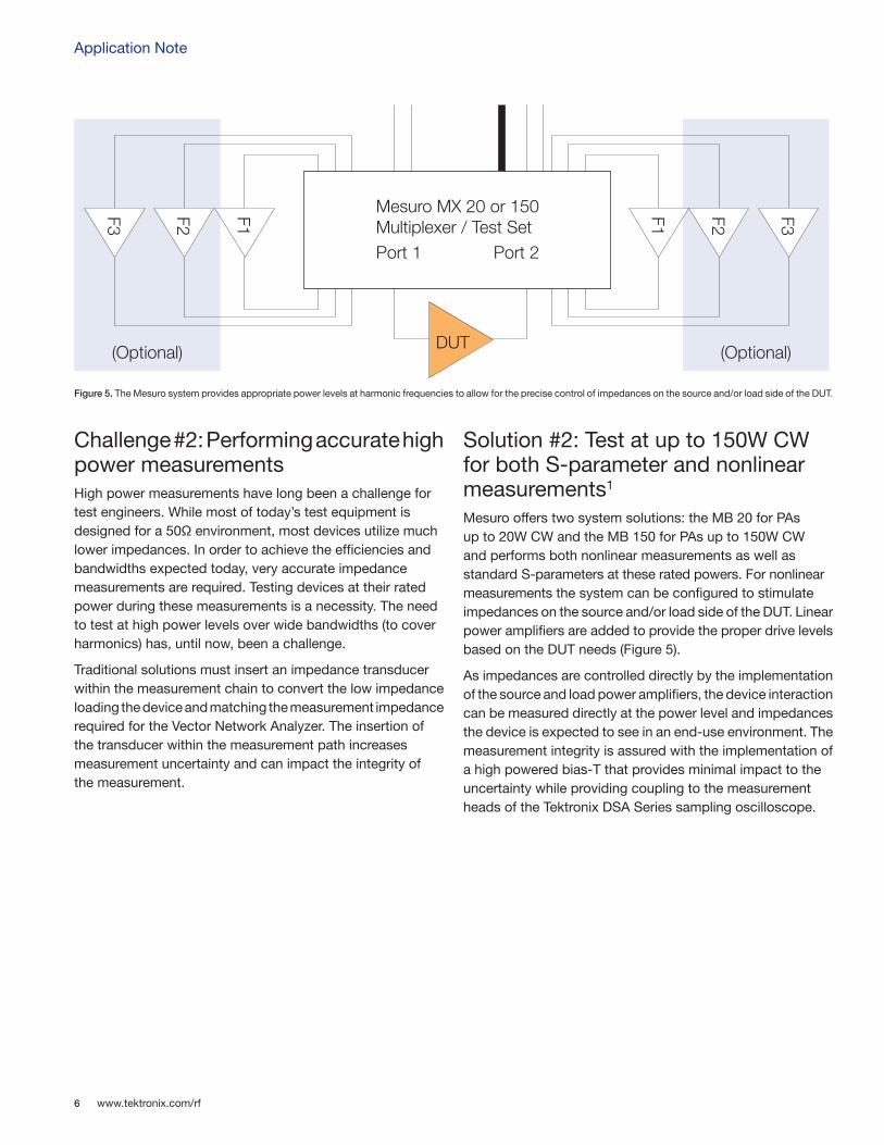
Challenge #2: Performing accurate high power measurementsHigh power measurements have long been a challenge for test engineers. While most of today’s test equipment is designed for a 50Ω environment, most devices utilize much lower impedances. In order to achieve the efficiencies and bandwidths expected today, very accurate impedance measurements are required. Testing devices at their rated power during these measurements is a necessity. The need to test at high power levels over wide bandwidths (to cover harmonics) has, until now, been a challenge.
Traditional solutions must insert an impedance transducer within the measurement chain to convert the low impedance loading the device and matching the measurement impedance required for the Vector Network Analyzer. The insertion of the transducer within the measurement path increases measurement uncertainty and can impact the integrity of the measurement.
Solution #2: Test at up to 150W CW for both S-parameter and nonlinear measurements1
Mesuro offers two system solutions: the MB 20 for PAs up to 20W CW and the MB 150 for PAs up to 150W CW and performs both nonlinear measurements as well as standard S-parameters at these rated powers. For nonlinear measurements the system can be configured to stimulate impedances on the source and/or load side of the DUT. Linear power amplifiers are added to provide the proper drive levels based on the DUT needs (Figure 5).
As impedances are controlled directly by the implementation of the source and load power amplifiers, the device interaction can be measured directly at the power level and impedances the device is expected to see in an end-use environment. The measurement integrity is assured with the implementation of a high powered bias-T that provides minimal impact to the uncertainty while providing coupling to the measurement heads of the Tektronix DSA Series sampling oscilloscope.
Figure 5. The Mesuro system provides appropriate power levels at harmonic frequencies to allow for the precise control of impedances on the source and/or load side of the DUT.
(Optional) DUT
F3 F2 F1
(Optional)
F3F2F1Mesuro MX 20 or 150Multiplexer / Test SetPort 1 Port 2

www.tektronix.com/rf 7
Overcoming Nonlinear Measurement Challenges
Challenge #3: Gap between measured results and fundamental circuit theoryRF engineers are taught how semiconductor devices and amplifiers respond to applied current and voltage waveforms. We know that the input voltage generates a current at the output, which in turn varies with an increasing output voltage. The resulting IV output plots, constrained by the device IV plane, can be then directly used to identify an optimum load that will draw maximum power out of the device. Yet, as soon RF engineers emerge into the practical life of RF and high-frequency engineering these basic knowledge and design fundamentals are quickly jettisoned in favor of other concepts such as the small-signal theory and measurements.
Admittedly, small signal parameters contain lots of relevant information enabling amplifier designs that maximize and eventually trade-off key performance figures such as output power, gain, and bandwidth for a given device. The same design principles are applicable even when the device is in a large-signal state, due to its drive level and bias point, and when the device is generating a significant harmonic content. The harmonic content that is directly produced by the current generator or device is typically reduced with a high-frequency filter at its output. This filter takes the form of a large output capacitance and other components that are contained within the device and eventually its package.
Unfortunately when performing small-signal measurements a number of key parameters, such as output power, efficiency or reliability, can be determined but it is often difficult to explain the results. It is exactly here where a PA designer gets frustrated with the lack of insight needed to identify any underlying problems and take corrective measures. Without this understanding, designers are forced to start iterating subtle design parameters, such as fundamental load and bias, and observe their impact. If this is done often enough with a particular device and amplifier design, the resulting experience will allow incremental design improvements. This design methodology works well until designers are asked to use a new device technology or develop a new type of amplifier, such as a Doherty or Envelope Tracking PA. In this case, a large portion of the existing experience becomes irrelevant, making new designs time consuming. In addition, through the continuous race for improved performance, new device
technologies and amplifier architectures are being introduced; however, any improvements often come at a price. For instance, new GaN devices offer high power densities and efficient operation, but to achieve this, designers need to start taking into account harmonic load and in some cases even harmonic source impedances. This introduces more parameters to be investigated and iterated during the PA design phase, leaving designers with multi-dimensional parameters with an almost infinite number of combinations.
Solution #3: Waveform engineering connects measured results with fundamental circuit theory So why did designers end up in a position so distant from the fundamental concept of current and voltage waveforms? At first glance, this question appears to relate directly to available microwave receiver measurement technology, as the measurement of waveforms requires the capture and calibration of broadband multi-octave signals. In fact, to capture a genuine waveform requires the detection of all relevant spectral components ranging from DC, baseband, fundamental to the highest harmonic frequency of interest. Traditional receivers, such as nonlinear VNAs, and calibration techniques have been recently introduced indicating the awareness within the established providers of RF measurement systems to go beyond the small-signal parameters. How-ever, the underlying measurement technology needs to go further than just the measurement of I & V waveforms. If a device is placed into a measurement system that captures the existing waveforms, the collected information provides details regarding the output power and efficiency, but provides little insight on how to improve the performance. The main reason is the 50 ohm characteristic impedance of measurement systems. While this works perfectly for small signal measurements, it is a rare event when the 50 ohms constitute an optimum loading for a large-signal device.
Basically the RF I & V waveforms are an advancement, but what is really needed is the creation of very specific set of waveforms that will result in characterizations of a device that will give an improved performance such as those offered by a number PA operational modes such as class-B, C, E, F, F-1, or even the Doherty PA.
Application Note
www.tektronix.com/rf8
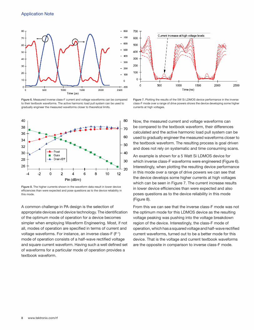
A common challenge in PA design is the selection of appropriate devices and device technology. The identification of the optimum mode of operation for a device becomes simpler when employing Waveform Engineering. Most, if not all, modes of operation are specified in terms of current and voltage waveforms. For instance, an inverse class-F (F-1) mode of operation consists of a half-wave rectified voltage and square current waveform. Having such a well defined set of waveforms for a particular mode of operation provides a textbook waveform.
Now, the measured current and voltage waveforms can be compared to the textbook waveform, their differences calculated and the active harmonic load pull system can be used to gradually engineer the measured waveforms closer to the textbook waveform. The resulting process is goal driven and does not rely on systematic and time consuming scans.
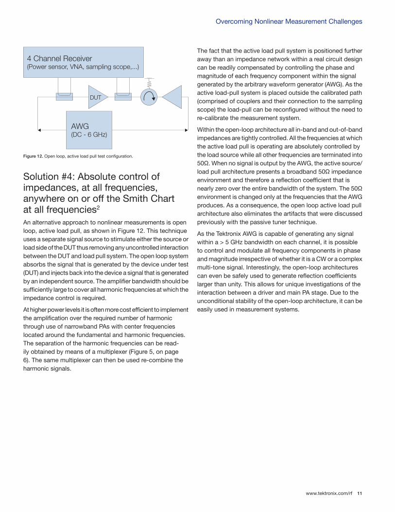
An example is shown for a 5 Watt Si LDMOS device for which inverse class-F waveforms were engineered (Figure 6). Interestingly, when plotting the resulting device performance in this mode over a range of drive powers we can see that the device develops some higher currents at high voltages which can be seen in Figure 7. The current increase results in lower device efficiencies than were expected and also poses questions as to the device reliability in this mode (Figure 8).
From this we can see that the inverse class-F mode was not the optimum mode for this LDMOS device as the resulting voltage peaking was pushing into the voltage breakdown region of the device. Interestingly, the class-F mode of operation, which has a squared voltage and half-wave rectified current waveforms, turned out to be a better mode for this device. That is the voltage and current textbook waveforms are the opposite in comparison to inverse class-F mode.
Figure 6. Measured inverse class-F current and voltage waveforms can be compared to their textbook waveforms. The active harmonic load pull system can be used to gradually engineer the measured waveforms closer to theoretical limits.
Figure 8. The higher currents shown in the waveform data result in lower device efficiencies than were expected and pose questions as to the device reliability in this mode.
Figure 7. Plotting the results of the 5W Si LDMOS device performance in the inverse class-F mode over a range of drive powers shows the device developing some higher currents at high voltages.

www.tektronix.com/rf 9
Overcoming Nonlinear Measurement Challenges
Applying Waveform Engineering, a clear class-F operation was obtained exhibiting very high efficiencies (Figure 9). These efficiencies are actually close to the theoretically maximum values when taking into account the finite knee voltage, and the number of optimally terminated harmonic impedances. During input power sweeps in this mode the device did not exhibit any of current rises within the high voltage region eliminating any reliability concerns of this device that were seen during the inverse class-F mode investigations.
These initial investigations were done at 0.9 GHz achieving drain efficiencies up to 79%. Past experience with this device seemed to indicate a barrier at frequencies above 1.6 GHz with all reported efficiencies for this device technology being below 70%. After establishing a good starting point at 0.9 GHz the investigations were extended to gradually increase the fundamental frequency up to 2.1 GHz. The achieved results at 2.1 GHz are shown in Figure 10 and are replicating very closely (78%) the high efficiencies that were achieved at the lower frequencies. The depicted waveforms at 2.1 GHz exhibit greater distortions as the device is operating closer to the transition frequency, f
t. These additional nonlinear effects make it more challenging to achieve a highly efficient mode of operation making this mode really difficult to find without the use of waveforms.
It is also interesting to note here is that the measured RF waveforms initially included the effects of device & package parasitics resulting in waveforms that lack any correlation with the device DC characteristics, which serve in all amplifiers as a reference. This is the direct result of the DC and RF measurement planes being at different locations, with the device & package parasitics being almost transparent at DC frequencies. To align both measurement planes, Mesuro has developed a software-based waveform de-embedding tool that allows for the de-embedding of the linear device and package parasitics from the RF waveforms.
The Mesuro system offers a bridge between the fundamental nonlinear circuit theory, that is based on current and voltage waveforms, and practical PA circuit design. Waveform Engineering offers the opportunity to systematically identify underlying technology and design issues that prevent designers from reaching theoretically possible performance. Designers can tackle new technologies without getting lost in the endless iterations of subtle parameters within a multi- dimensional parameter space and thus shorten the PA development cycle while ensuring a theoretically optimum design.
Figure 9. The same 5W Si LDMOS device operating at 900 MHz clearly achieves class-F mode, with an output power >36 dBm and efficiency as high as 79%.
Figure 10. The same LDMOS device was extended up to 2.1 GHz and also achieved >36 dBm with an efficiency up to 78%.

Application Note
www.tektronix.com/rf10
Challenge #4: Achieving precise impedance control over the entire Smith ChartDesigning a highly efficient PA is coupled to the precise control of the fundamental and harmonic impedances that are presented to the device. It is therefore critical that the designer be able to measure what is needed at relevant power levels and frequencies, with the signal complexity that is required for a given application.
Passive load pull solutions have been a valuable tool for device and PA designers over the years. A power sensor, VNA or sampling scope can be used for nonlinear measurements as shown in Figure 11. Tuners allow for tuning impedance values of the harmonics at the device under test (DUT) input and output. This provides impedance values for designing matching circuits and power levels. A typical configuration consists of one tuner at the input, to reduce the mismatch between the input source and the device under test, and one tuner at the output to generate the required loading condition. Tuner positioning is highly accurate and repeatable and this allows them to be calibrated. During the calibration an accurate relationship is established between the position of the slug and the sliding short. Based on this calibration stage, the power inserted into the DUT can be determined from the power level set by the input source while the output power can be then calculated from the power sensor reading.
The biggest disadvantage of these systems is that they generate impedances over a large frequency range, but can control the impedance at only one single frequency. The impedance control is achieved by positioning the slug,
which physically affects all remaining frequencies over which the tuner can be operated. Consequently, all harmonic impedances are not only uncontrollable, but also change their value with every new position resulting in measurement artifacts that are not representative of real circuits. This can lead to significant performance variations between the load-pull measurements and the realized power amplifier performance.
The same disadvantage is valid for harmonic tuners (passive tuners with multiple slugs and sliding shorts) that allow a limited control of harmonic impedances as the higher harmonics (above 3rd harmonic) are not controlled and still have large variance from real circuits. For instance, a small current coming from the DUT can be transformed, due to ohm’s law, into a very large voltage with harmonic impedances (above 3rd harmonic) that are easily generated by the tuners. The uncontrolled load variations make it impossible to achieve clean waveforms as required for waveform engineering as they will introduce significant capacitive and inductive loading making the waveforms highly distorted.
The position of the passive tuner between the DUT and the measuring receiver (as shown in Figure 11) makes it difficult to distinguish artifacts from the tuner and the DUT itself. This effect then has potential impact on the input or output matching network in a PA (power amplifier) design. Due to the losses between the DUT and the tuners only part of the Smith Chart can be covered. At lower frequencies this effect is mitigated by the relatively low losses however can increase significantly for higher frequencies such as the harmonics of a signal.
Additionally, the increased length (due to the physical size of the tuners) will produce a larger phase variation and introduce measurement artifacts that differ from real circuits. For instance, it has been shown that a phase difference of only a few degrees can introduce artifacts that resemble memory effects. In addition, these impedance artifacts are changing with each impedance setting (due to the varying positioning of the slug) and it is therefore very challenging to account for them. Such phase variations can readily occur when utilizing wideband modulated signals such as in W-CDMA or LTE systems or narrowband systems with multiple channels.
Figure 11. Typical passive source / load pull test configuration.
DUTTuner Tuner
4 Channel Receiver(Power sensor, VNA, sampling scope,...)
www.tektronix.com/rf 11
Overcoming Nonlinear Measurement Challenges
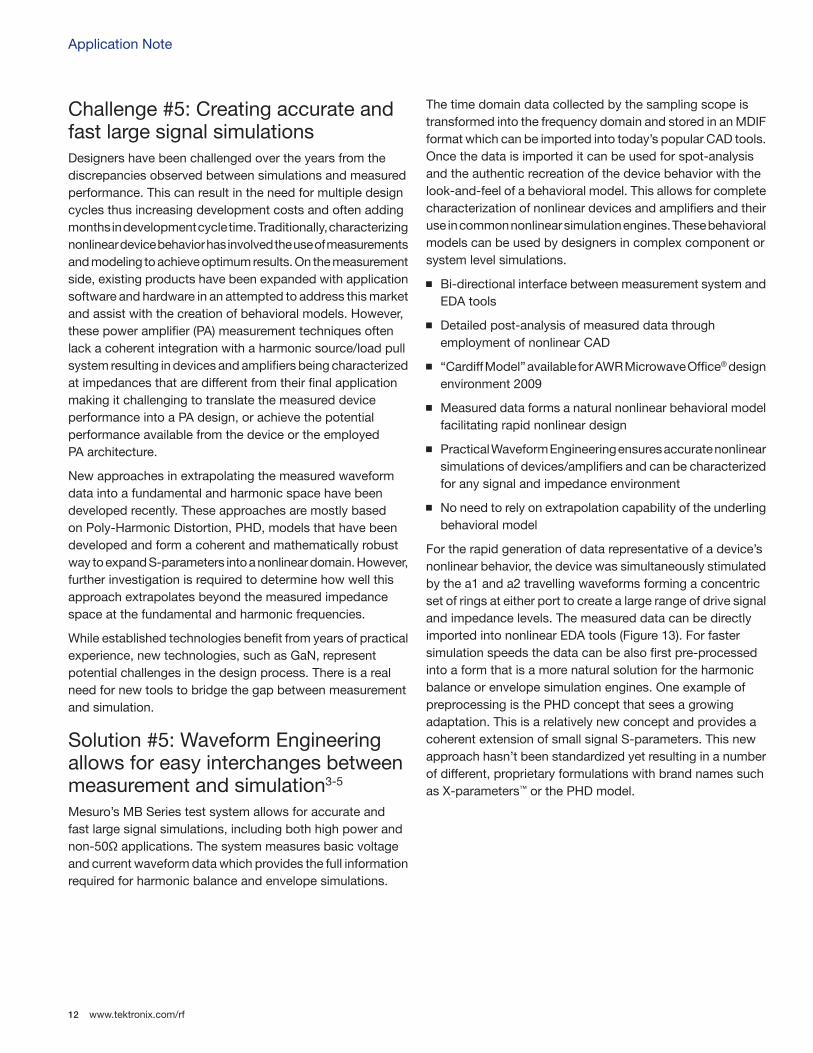
Solution #4: Absolute control of impedances, at all frequencies, anywhere on or off the Smith Chart at all frequencies2
An alternative approach to nonlinear measurements is open loop, active load pull, as shown in Figure 12. This technique uses a separate signal source to stimulate either the source or load side of the DUT thus removing any uncontrolled interaction between the DUT and load pull system. The open loop system absorbs the signal that is generated by the device under test (DUT) and injects back into the device a signal that is generated by an independent source. The amplifier bandwidth should be sufficiently large to cover all harmonic frequencies at which the impedance control is required.
At higher power levels it is often more cost efficient to implement the amplification over the required number of harmonic through use of narrowband PAs with center frequencies located around the fundamental and harmonic frequencies. The separation of the harmonic frequencies can be read-ily obtained by means of a multiplexer (Figure 5, on page 6). The same multiplexer can then be used re-combine the harmonic signals.
The fact that the active load pull system is positioned further away than an impedance network within a real circuit design can be readily compensated by controlling the phase and magnitude of each frequency component within the signal generated by the arbitrary waveform generator (AWG). As the active load-pull system is placed outside the calibrated path (comprised of couplers and their connection to the sampling scope) the load-pull can be reconfigured without the need to re-calibrate the measurement system.
Within the open-loop architecture all in-band and out-of-band impedances are tightly controlled. All the frequencies at which the active load pull is operating are absolutely controlled by the load source while all other frequencies are terminated into 50Ω. When no signal is output by the AWG, the active source/load pull architecture presents a broadband 50Ω impedance environment and therefore a reflection coefficient that is nearly zero over the entire bandwidth of the system. The 50Ω environment is changed only at the frequencies that the AWG produces. As a consequence, the open loop active load pull architecture also eliminates the artifacts that were discussed previously with the passive tuner technique.
As the Tektronix AWG is capable of generating any signal within a > 5 GHz bandwidth on each channel, it is possible to control and modulate all frequency components in phase and magnitude irrespective of whether it is a CW or a complex multi-tone signal. Interestingly, the open-loop architectures can even be safely used to generate reflection coefficients larger than unity. This allows for unique investigations of the interaction between a driver and main PA stage. Due to the unconditional stability of the open-loop architecture, it can be easily used in measurement systems.
Figure 12. Open loop, active load pull test configuration.
4 Channel Receiver(Power sensor, VNA, sampling scope,...)
AWG(DC - 6 GHz)
DUT
Application Note
www.tektronix.com/rf12
Challenge #5: Creating accurate and fast large signal simulationsDesigners have been challenged over the years from the discrepancies observed between simulations and measured performance. This can result in the need for multiple design cycles thus increasing development costs and often adding months in development cycle time. Traditionally, characterizing nonlinear device behavior has involved the use of measurements and modeling to achieve optimum results. On the measurement side, existing products have been expanded with application software and hardware in an attempted to address this market and assist with the creation of behavioral models. However, these power amplifier (PA) measurement techniques often lack a coherent integration with a harmonic source/load pull system resulting in devices and amplifiers being characterized at impedances that are different from their final application making it challenging to translate the measured device performance into a PA design, or achieve the potential performance available from the device or the employed PA architecture.
New approaches in extrapolating the measured waveform data into a fundamental and harmonic space have been developed recently. These approaches are mostly based on Poly-Harmonic Distortion, PHD, models that have been developed and form a coherent and mathematically robust way to expand S-parameters into a nonlinear domain. However, further investigation is required to determine how well this approach extrapolates beyond the measured impedance space at the fundamental and harmonic frequencies.
While established technologies benefit from years of practical experience, new technologies, such as GaN, represent potential challenges in the design process. There is a real need for new tools to bridge the gap between measurement and simulation.
Solution #5: Waveform Engineering allows for easy interchanges between measurement and simulation3-5
Mesuro’s MB Series test system allows for accurate and fast large signal simulations, including both high power and non-50Ω applications. The system measures basic voltage and current waveform data which provides the full information required for harmonic balance and envelope simulations.
The time domain data collected by the sampling scope is transformed into the frequency domain and stored in an MDIF format which can be imported into today’s popular CAD tools. Once the data is imported it can be used for spot-analysis and the authentic recreation of the device behavior with the look-and-feel of a behavioral model. This allows for complete characterization of nonlinear devices and amplifiers and their use in common nonlinear simulation engines. These behavioral models can be used by designers in complex component or system level simulations.
Bi-directional interface between measurement system and EDA tools
Detailed post-analysis of measured data through employment of nonlinear CAD
“Cardiff Model” available for AWR Microwave Office® design environment 2009
Measured data forms a natural nonlinear behavioral model facilitating rapid nonlinear design
Practical Waveform Engineering ensures accurate nonlinear simulations of devices/amplifiers and can be characterized for any signal and impedance environment
No need to rely on extrapolation capability of the underling behavioral model
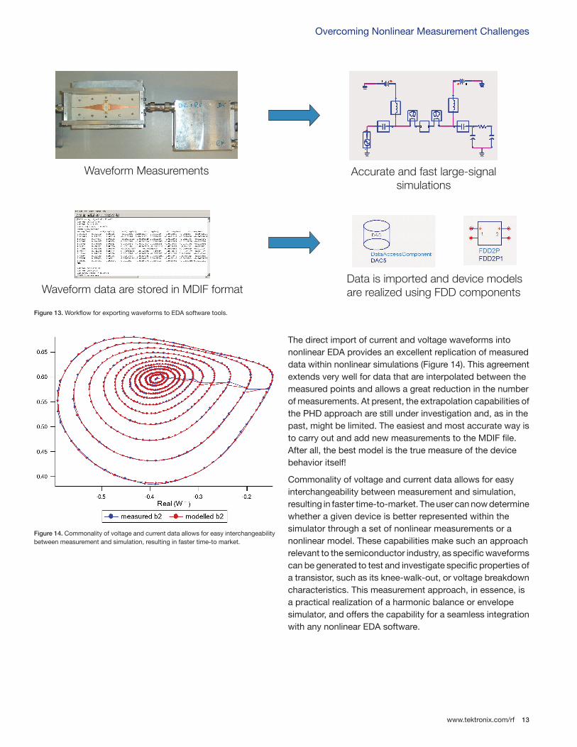
For the rapid generation of data representative of a device’s nonlinear behavior, the device was simultaneously stimulated by the a1 and a2 travelling waveforms forming a concentric set of rings at either port to create a large range of drive signal and impedance levels. The measured data can be directly imported into nonlinear EDA tools (Figure 13). For faster simulation speeds the data can be also first pre-processed into a form that is a more natural solution for the harmonic balance or envelope simulation engines. One example of preprocessing is the PHD concept that sees a growing adaptation. This is a relatively new concept and provides a coherent extension of small signal S-parameters. This new approach hasn’t been standardized yet resulting in a number of different, proprietary formulations with brand names such as X-parameters™ or the PHD model.
www.tektronix.com/rf 13
Overcoming Nonlinear Measurement Challenges
The direct import of current and voltage waveforms into nonlinear EDA provides an excellent replication of measured data within nonlinear simulations (Figure 14). This agreement extends very well for data that are interpolated between the measured points and allows a great reduction in the number of measurements. At present, the extrapolation capabilities of the PHD approach are still under investigation and, as in the past, might be limited. The easiest and most accurate way is to carry out and add new measurements to the MDIF file. After all, the best model is the true measure of the device behavior itself!
Commonality of voltage and current data allows for easy interchangeability between measurement and simulation, resulting in faster time-to-market. The user can now determine whether a given device is better represented within the simulator through a set of nonlinear measurements or a nonlinear model. These capabilities make such an approach relevant to the semiconductor industry, as specific waveforms can be generated to test and investigate specific properties of a transistor, such as its knee-walk-out, or voltage breakdown characteristics. This measurement approach, in essence, is a practical realization of a harmonic balance or envelope simulator, and offers the capability for a seamless integration with any nonlinear EDA software.
Figure 13. Workflow for exporting waveforms to EDA software tools.
Figure 14. Commonality of voltage and current data allows for easy interchangeability between measurement and simulation, resulting in faster time-to market.
Waveform Measurements Accurate and fast large-signalsimulations
Data is imported and device modelsare realized using FDD componentsWaveform data are stored in MDIF format

Application Note
www.tektronix.com/rf14
Challenge #6: Achieving high efficiency across wide bandwidthsPower amplifier designs for wireless communication have traditionally been focused on applications within a single band of interest, i.e. specified spectrum allocation for a regional service with a fractional RF bandwidths of 5% or less. These narrowband PAs have been able to achieve operating efficiencies above 75% by relying heavily on precise multi-harmonic impedance terminations at the DUT as well as very high levels of device gain-compression.
When you combine the demand for the amplifier to be able to operate over multiple bands of interest and new spectrum allocations for new wireless applications, such as WiMax and 4G, the amplifiers will likely be require to operate across a much wider bandwidths. This is attributed to not only wider spectral allocations and multi-band implementations, but also the base bandwidth of the signals themselves which may well extend up to, and ultimately exceed, 100 MHz. The need for wider bandwidths is driving the development of new device technologies such as GaN and new modes of operation such as Class-J. GaN HFETs are an ideal technology for PAs due to their good thermal performance and their capabilities for high frequency and high power operation. The Class-J mode of operation has shown theoretical potential of obtaining linear RF PAs that have the same efficiency and linearity as conventional Class-AB designs but do not re-quire a band limiting harmonic short.
As the demand for wider operational bandwidths and improved efficiencies drive designers towards new tech-nologies and designs, the need for improved measurement techniques and models is increasing. Designers need mea-surement solutions which will provide the insight needed to identify underlying problems and enable corrective actions to speed their development cycle.
Solution #6: Waveform engineering optimizes performance and reduces design cycles6-8
The Mesuro active load pull technology offers key new insights into the development of new technologies for broadband PA design. The following example highlights results from the development of a class-J mode PA using a GaN HEMT power transistor. By starting with the theoretical waveforms for a class-J PA defined by Cripps, a waveform engineering-based process was first used to optimize the device and then, later, the PA. Waveform and systematic load pull measurement data has been used in the development stage of the design procedure, while also being used to analyze the extent to which optimum broadband high-efficiency operation has been achieved in this mode.
The theoretical class-J design displays approximate half-wave rectified sinusoidal output current and voltage waveforms, with a phase overlap between the two (Figure 15). This mode of operation lends itself very well to the process of waveform engineering, as independent bias control and active multi- harmonic load pull were used to engineer the shape of the current and voltage waveforms respectively.
Figure 15. Measured class-J waveforms on a 10W GaN HEMT.
www.tektronix.com/rf 15
Overcoming Nonlinear Measurement Challenges
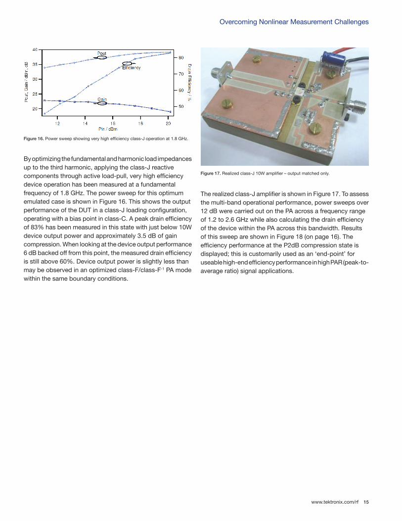
By optimizing the fundamental and harmonic load impedances up to the third harmonic, applying the class-J reactive components through active load-pull, very high efficiency device operation has been measured at a fundamental frequency of 1.8 GHz. The power sweep for this optimum emulated case is shown in Figure 16. This shows the output performance of the DUT in a class-J loading configuration, operating with a bias point in class-C. A peak drain efficiency of 83% has been measured in this state with just below 10W device output power and approximately 3.5 dB of gain compression. When looking at the device output performance 6 dB backed off from this point, the measured drain efficiency is still above 60%. Device output power is slightly less than may be observed in an optimized class-F/class-F-1 PA mode within the same boundary conditions.
The realized class-J amplifier is shown in Figure 17. To assess the multi-band operational performance, power sweeps over 12 dB were carried out on the PA across a frequency range of 1.2 to 2.6 GHz while also calculating the drain efficiency of the device within the PA across this bandwidth. Results of this sweep are shown in Figure 18 (on page 16). The efficiency performance at the P2dB compression state is displayed; this is customarily used as an ‘end-point’ for useable high-end efficiency performance in high PAR (peak-to-average ratio) signal applications.
Figure 16. Power sweep showing very high efficiency class-J operation at 1.8 GHz.
Figure 17. Realized class-J 10W amplifier – output matched only.

Application Note
www.tektronix.com/rf16
Figure 19. By expanding the class-J theory and identifying a larger range of harmonic terminations the bandwidth was extended from 1.4 to 2.6 GHz with greater than 60% efficiency!
As seen in Figure 18, the measured P2dB drain efficiency for the realized class-J amplifier is between 60-70% between 1.35 GHz and 2.25 GHz; a 50% bandwidth about a center frequency of 1.8 GHz. Within this bandwidth output power from the amplifier is between 9 and 11.5Watts.
Building on the first pass design, the Mesuro system was used to expand the class-J theory and identified a larger range of harmonic terminations. The second pass design (Figure 19) extended the bandwidth from 1.4 to 2.6 GHz with greater than 60% efficiency!
Figure 18. P2dB drain efficiency, Pout performance, and device model-predicted efficiency for the realized class-J PA across a bandwidth of 1.2-2.5 GHz.
www.tektronix.com/rf 17
Overcoming Nonlinear Measurement Challenges
Figure 20. Output spectrum from class-J PA, measuring ACP for a 5 MHz WCDMA signal at center frequency 1.8 GHz, 39% average efficiency.
Figure 21. Average class-J PA performance with a power-swept 5 MHz WCDMA signal at center frequency of 1.8 GHz.
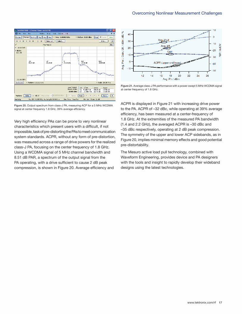
Very high efficiency PAs can be prone to very nonlinear characteristics which present users with a difficult, if not impossible, task of pre-distorting the PAs to meet communication system standards. ACPR, without any form of pre-distortion, was measured across a range of drive powers for the realized class-J PA, focusing on the center frequency of 1.8 GHz. Using a WCDMA signal of 5 MHz channel bandwidth and 8.51 dB PAR, a spectrum of the output signal from the PA operating, with a drive sufficient to cause 2 dB peak compression, is shown in Figure 20. Average efficiency and
ACPR is displayed in Figure 21 with increasing drive power to the PA. ACPR of –32 dBc, while operating at 39% average efficiency, has been measured at a center-frequency of 1.8 GHz. At the extremities of the measured PA bandwidth (1.4 and 2.2 GHz), the averaged ACPR is –30 dBc and –35 dBc respectively, operating at 2 dB peak compression. The symmetry of the upper and lower ACP sidebands, as in Figure 20, implies minimal memory effects and good potential pre-distortability.
The Mesuro active load pull technology, combined with Waveform Engineering, provides device and PA designers with the tools and insight to rapidly develop their wideband designs using the latest technologies.

Application Note
www.tektronix.com/rf18
Challenge #7: New technologies drive the need for improved reliability testing and insight9-13
New technologies, such as GaN HFETs, are an ideal technology for radio frequency (RF) power amplifier applications due to their good thermal performance and their capabilities for high frequency and high power operation. However, as with any developmental transistor technology, GaN HFETs must demonstrate robust performance before they can be utilized in end-use applications. In order to demonstrate robust performance, a new semiconductor process must be capable of a level of constant performance
over a life cycle appropriate for its end application. Investigations of reliability in RF transistors employ a fairly standard characterization procedure whereby RF output power reduction, gain reduction, DC bias drift, and leakage levels are measured before, during and after various RF and DC stress tests. Reports of GaN HFET degradation characteristics measured using these standard techniques have become increasingly common as the technology approaches maturity. Design engineers need tools that can provide insight into potential design issues that may reduce the life span of their fielded products.
Solution #7: Waveform Engineering provides design insight into reliability and stress issues In this example, Waveform Engineering is used to monitor degradation in developmental RF transistor GaN technologies. RF waveform measurements were used to monitor device performance during large signal continuous wave (CW) RF stress testing. The ability to measure current and voltage waveforms at the device input and output sampled during the stress period gives a unique insight into the degradation mechanisms. The GaN devices were shown to have rapid degradation issues during their burn-in period and the effects of high field and high channel current led degradation were separated in order to advance the diagnosis of device material and processing issues. Several devices from the same wafer were used in the testing. Each device was stressed for a period of 1.5 hours while the input and output current and voltage waveforms were periodically sampled 100 times, resulting in a measurement similar to an RF burn-in test.
The results in Figure 22 show standard RF and DC reliability results. More than 10% of the initial output power is lost over the total stress period. The observed increase in DC gate leakage current and the decreased DC drain current are consistent with trap generation and charge storage on the drain side of the gate.
Figure 22. Standard RF (top) and DC (bottom) measures of degradation for a 1.5 hour burn-in period measured in Class A at Vd = 20V with an optimal POUT tuned load at f0.
www.tektronix.com/rf 19
Overcoming Nonlinear Measurement Challenges
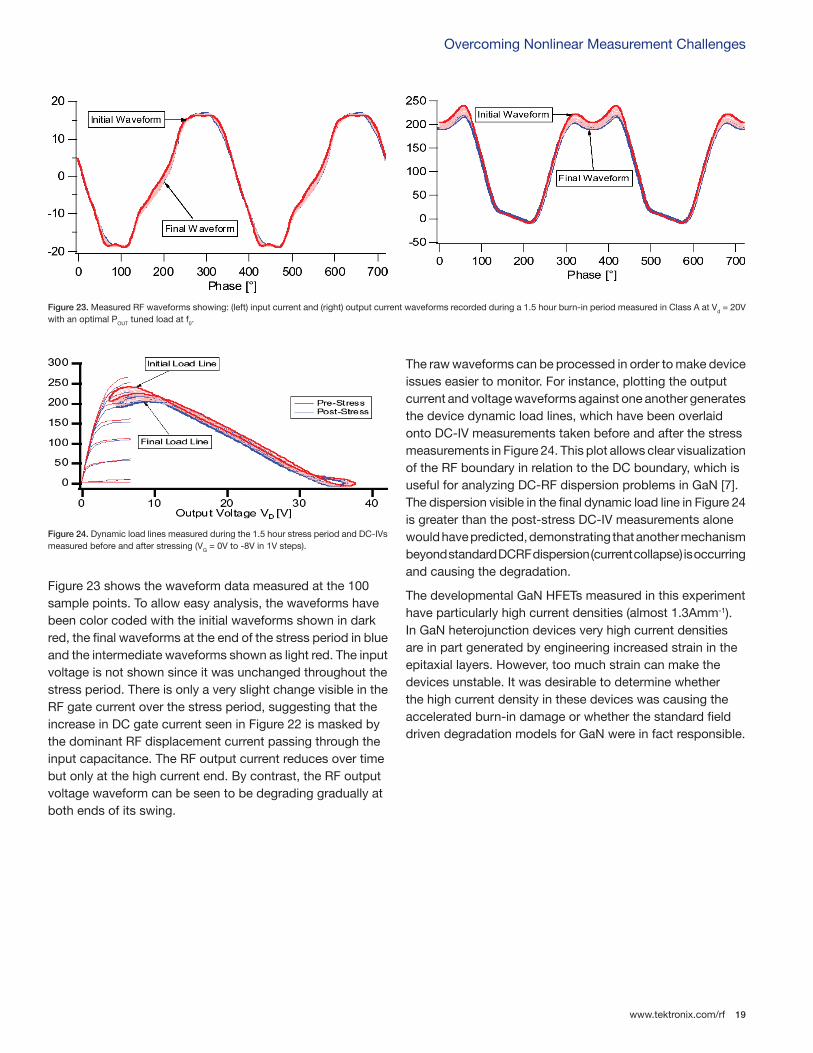
Figure 23 shows the waveform data measured at the 100 sample points. To allow easy analysis, the waveforms have been color coded with the initial waveforms shown in dark red, the final waveforms at the end of the stress period in blue and the intermediate waveforms shown as light red. The input voltage is not shown since it was unchanged throughout the stress period. There is only a very slight change visible in the RF gate current over the stress period, suggesting that the increase in DC gate current seen in Figure 22 is masked by the dominant RF displacement current passing through the input capacitance. The RF output current reduces over time but only at the high current end. By contrast, the RF output voltage waveform can be seen to be degrading gradually at both ends of its swing.
The raw waveforms can be processed in order to make device issues easier to monitor. For instance, plotting the output current and voltage waveforms against one another generates the device dynamic load lines, which have been overlaid onto DC-IV measurements taken before and after the stress measurements in Figure 24. This plot allows clear visualization of the RF boundary in relation to the DC boundary, which is useful for analyzing DC-RF dispersion problems in GaN [7]. The dispersion visible in the final dynamic load line in Figure 24 is greater than the post-stress DC-IV measurements alone would have predicted, demonstrating that another mechanism beyond standard DCRF dispersion (current collapse) is occurring and causing the degradation.
The developmental GaN HFETs measured in this experiment have particularly high current densities (almost 1.3Amm-1). In GaN heterojunction devices very high current densities are in part generated by engineering increased strain in the epitaxial layers. However, too much strain can make the devices unstable. It was desirable to determine whether the high current density in these devices was causing the accelerated burn-in damage or whether the standard field driven degradation models for GaN were in fact responsible.
Figure 24. Dynamic load lines measured during the 1.5 hour stress period and DC-IVs measured before and after stressing (VG = 0V to -8V in 1V steps).
Figure 23. Measured RF waveforms showing: (left) input current and (right) output current waveforms recorded during a 1.5 hour burn-in period measured in Class A at Vd = 20V with an optimal POUT tuned load at f0.
Application Note
www.tektronix.com/rf20
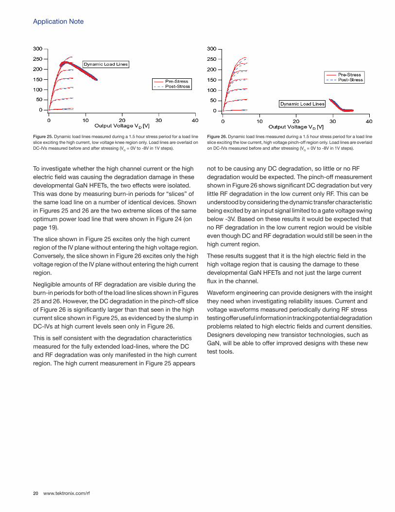
Figure 25. Dynamic load lines measured during a 1.5 hour stress period for a load line slice exciting the high current, low voltage knee region only. Load lines are overlaid on DC-IVs measured before and after stressing (VG = 0V to -8V in 1V steps).
Figure 26. Dynamic load lines measured during a 1.5 hour stress period for a load line slice exciting the low current, high voltage pinch-off region only. Load lines are overlaid on DC-IVs measured before and after stressing (VG = 0V to -8V in 1V steps).
To investigate whether the high channel current or the high electric field was causing the degradation damage in these developmental GaN HFETs, the two effects were isolated. This was done by measuring burn-in periods for “slices” of the same load line on a number of identical devices. Shown in Figures 25 and 26 are the two extreme slices of the same optimum power load line that were shown in Figure 24 (on page 19).
The slice shown in Figure 25 excites only the high current region of the IV plane without entering the high voltage region. Conversely, the slice shown in Figure 26 excites only the high voltage region of the IV plane without entering the high current region.
Negligible amounts of RF degradation are visible during the burn-in periods for both of the load line slices shown in Figures 25 and 26. However, the DC degradation in the pinch-off slice of Figure 26 is significantly larger than that seen in the high current slice shown in Figure 25, as evidenced by the slump in DC-IVs at high current levels seen only in Figure 26.
This is self consistent with the degradation characteristics measured for the fully extended load-lines, where the DC and RF degradation was only manifested in the high current region. The high current measurement in Figure 25 appears
not to be causing any DC degradation, so little or no RF degradation would be expected. The pinch-off measurement shown in Figure 26 shows significant DC degradation but very little RF degradation in the low current only RF. This can be understood by considering the dynamic transfer characteristic being excited by an input signal limited to a gate voltage swing below -3V. Based on these results it would be expected that no RF degradation in the low current region would be visible even though DC and RF degradation would still be seen in the high current region.
These results suggest that it is the high electric field in the high voltage region that is causing the damage to these developmental GaN HFETs and not just the large current flux in the channel.
Waveform engineering can provide designers with the insight they need when investigating reliability issues. Current and voltage waveforms measured periodically during RF stress testing offer useful information in tracking potential degradation problems related to high electric fields and current densities. Designers developing new transistor technologies, such as GaN, will be able to offer improved designs with these new test tools.
www.tektronix.com/rf 21
Overcoming Nonlinear Measurement Challenges
Challenge #8: Optimizing harmonic terminations1, 8, 14-17
The large voltage swing associated with inverse class-F operation, that is key to the high power and high efficiencies achievable in this mode of operation, can often be difficult to realize with many current device technologies (e.g. LDMOS, GaAs) due to the limitations induced by device breakdown voltages. Today, with advancements in wide band-gap semi-conductor technologies (GaN, SiC), large rail voltages become feasible, hence allowing for power amplifiers with very high efficiency performance to be realized. The ability to accurately optimize harmonic terminations at the fundamental and higher order harmonics is essential for designers to achieve their performance goals. Existing measurement solutions struggle to maintain this accuracy with the higher order harmonics. New technologies have the possibility of extending development cycles for designers as they push toward higher power and higher efficiencies.
Solution #8: Active load pull offers advanced capabilities to determine harmonic terminations on either source or load sideThe Mesuro system was used to develop an inverse class-F design procedure for obtaining very high efficiency performance at high power levels. In this example, a 10W GaN HEMT was used to develop a multi-band solution at two fundamental frequencies of 0.9 GHz and 2.1 GHz.
First, an equivalent circuit model for the parasitic effects of the device package was generated to allow predictions for the required open and short terminations at the package-plane to be made. The utilized TRL calibration generates a measurement reference-plane at the device package and not, as is the case for on-wafer measurements, close to the device Igen.-plane. Thus, the approximated package network provides a means of predicting and analyzing operation at the Igen.-plane during the design process. This process is essential for enabling RF waveform engineering as it allows for correlation between the measured dynamic I-Vs and the device DC IV plane, which defines the boundaries of the device performance.
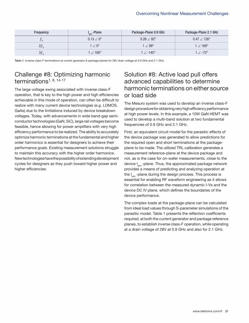
The complex loads at the package-plane can be calculated from ideal load values through S-parameter simulations of the parasitic model. Table 1 presents the reflection coefficients required, at both the current generator and package reference planes, to establish inverse class-F operation, while operating at a drain voltage of 28V at 0.9 GHz and also for 2.1 GHz.
Table 1. Inverse class-F terminations at current generator & package planes for 28V drain voltage at 0.9 GHz and 2.1 GHz.
Frequency Igen.-Plane Package-Plane 0.9 GHz Package-Plane 2.1 GHz
ƒ0 0.13 ∠ 0° 0.26 ∠ 82° 0.47 ∠ 126°
2ƒ0 1 ∠ 0° 1 ∠ 99° 1 ∠ 169°
3ƒ0 1 ∠ 180° 1 ∠ -145° 1 ∠ -72°

Application Note
www.tektronix.com/rf22
The ideal inverse class-F output waveforms of half-wave rectified voltage and square current represent a perfectly functioning, 100% efficient inverse class-F amplifier. In reality, this ideal performance is compromised by DC offsets, as well as the ability to generate the perfect harmonic terminations required. Assuming terminations up to the fifth harmonic in the current waveform (through hitting the current boundary conditions), and up to the second harmonic in the voltage waveform (through active harmonic load pull waveform engineering), a bandwidth limitation factor is applicable to the ideal drain efficiency.
After selecting the optimum gate bias, the predicted load impedances in Table 1 (on page 21) were optimized. In a first step the fundamental load impedance at the Igen.-plane was swept between 60Ω and 70Ω. Once the optimum for the fundamental impedance was determined the phase of the second harmonic was swept by ±10° of the figure in Table 1 to compensate for any small errors in the approximated package model. The same sweep was then applied to the third harmonic phase. The resulting optimized impedance values at the Igen.-plane are given in Table 2.
A power sweep was conducted with the optimized gate bias, fundamental load and harmonic impedances. The results at 0.9 GHz are shown in Figure 27. The maximum efficiency achieved was 81.5%, at a gain compression of 4.5 dB and 40.9 dBm fundamental output power.
With the successful waveform optimization for inverse class-F at 0.9 GHz completed, performance scalability to higher frequencies was investigated. For this purpose the gate bias sweep was repeated at 2.1 GHz, this time delivering an optimum of Vgs = -2.5V.
Figure 27. Power sweep at 28V drain voltage bias condition at 0.9 GHz.
Table 2. Optimum terminations for Vds = 28V at 0.9 GHz.
Frequency Igen.-Plane Package-Plane
ƒ0 0.14 ∠ 0° 0.27 ∠ 86°
2ƒ0 1 ∠ -6° 1 ∠ 91°
3ƒ0 1 ∠ -174° 1 ∠ -142°
www.tektronix.com/rf 23
Overcoming Nonlinear Measurement Challenges
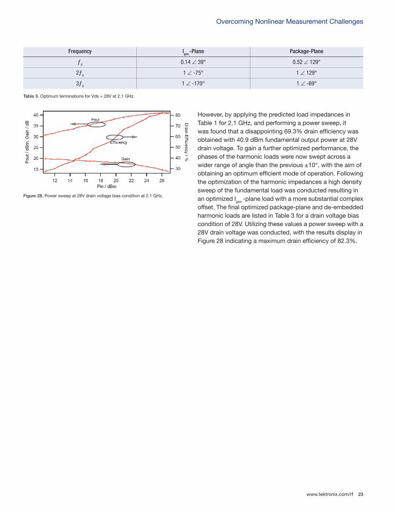
However, by applying the predicted load impedances in Table 1 for 2.1 GHz, and performing a power sweep, it was found that a disappointing 69.3% drain efficiency was obtained with 40.9 dBm fundamental output power at 28V drain voltage. To gain a further optimized performance, the phases of the harmonic loads were now swept across a wider range of angle than the previous ±10°, with the aim of obtaining an optimum efficient mode of operation. Following the optimization of the harmonic impedances a high density sweep of the fundamental load was conducted resulting in an optimized Igen.-plane load with a more substantial complex offset. The final optimized package-plane and de-embedded harmonic loads are listed in Table 3 for a drain voltage bias condition of 28V. Utilizing these values a power sweep with a 28V drain voltage was conducted, with the results display in Figure 28 indicating a maximum drain efficiency of 82.3%.
Figure 28. Power sweep at 28V drain voltage bias condition at 2.1 GHz.
Table 3. Optimum terminations for Vds = 28V at 2.1 GHz.
Frequency Igen.-Plane Package-Plane
ƒ0 0.14 ∠ 39° 0.52 ∠ 129°
2ƒ0 1 ∠ -75° 1 ∠ 129°
3ƒ0 1 ∠ -170° 1 ∠ -69°

Application Note
www.tektronix.com/rf24
Challenge #9: Low frequency limitations and applicationsThe drive for more efficient and lower cost designs is increasing for wireless communications at all frequency ranges. Commercial wireless applications have driven much of the power amplifier market at fundamental frequen-cies ranging from 0.8 GHz to 2.7 GHz. Today there are new opportunities for extending commercial wireless technolo-gies and applications in the 200 MHz to 800 MHz frequency bands.
In the lower part of the UHF band most of the commercial opportunities had long been held by the broadcasters of analog television. With the move to digital television and the subsequent reallocation of UHF band frequencies, some very attractive spectrum is being opened up. The US National Broadband Plan calls for the freeing up of 120 MHz of bandwidth in this new “white space”. A “White Spaces Coalition” has been formed by 8 major companies to influ-ence the regulations to enable a new high speed internet technology in this white space (Microsoft, Google, Dell, HP, Intel, Philips, Samsung, Earthlink). One option being con-sidered is creating a new White Space Network based on establishing a WLAN technology at UHF.
In the aerospace and defense market, satellite commu-nications (SATCOM) systems have long operated in the UHF band. However today, just like the commercial smart phones, the need for instant communication across more troops and including voice, video, and data is driving the next generation system specifications. For these UHF power amps, higher efficiency and linearity performance will be two required primary improvements. Improving efficiency is critical to meet the goal of reducing combat load, such as reducing spare battery weight. Higher efficiency will be criti-cal for battery life and thermal considerations. The goal is to achieve power efficiencies of >50%.
An expanding need for high efficiency UHF power ampli-fiers creates some interesting challenges for traditional measurement solutions. At UHF frequencies passive tuners represent a physical challenge as their size is proportional to wavelength (as shown in Table 1). The control of the reflection coefficients at lower frequencies is limited by the prohibitive length requirements for the coaxial line for the respective wavelength. Passive tuners that operate in the several hundreds of megahertz can be three feet long or more! Adding these tuners to either side of the DUT cre-ates a number of challenges. For on wafer applications, the tuner size and weight can add to the cost and complexity of the probe station. In addition there are vibration concerns as impedances on these large tuners are varied. The move to increase PA performance at UHF frequencies creates a unique problem for passive load pull.
Single Harmonic Multi Harmonic
Frequency Range 250 – 2500 MHz 400 – 3000 MHz
Number of Harmonics
1 3
Size (h x w x l
Inches
Meters
12 x 10 x 36.9
.31 x .25 x .94
12 x 13 x 51
.33 x .32 x 1.30
Table 1: Passive tuner size creates challenges at UHF frequencies.

www.tektronix.com/rf 25
Overcoming Nonlinear Measurement Challenges
Solution #9: Active load pull optimum solution for new UHF applicationsFor UHF applications the need for passive tuners and their physical size challenges disappears. With active load pull all impedance variations are created electronically. Elimi-nating the need for passive tuners removes the physical constraints for performing load pull measurements at low frequencies. Whether you are measuring at 2 GHz, 200 MHz, or 200 kHz becomes a function of your source and is no longer limited by wavelength.
As mentioned, for UHF applications (or lower), the fre-quency bandwidth of the AWG and the DSA series sampling scope both start at the DC frequency making it possible to perform very low frequency load-pull measurements. With > 5 GHz of bandwidth, the AWG is capable of covering frequencies from sub-Hertz to Gigahertz frequencies thus allowing the use of the open-loop architecture at baseband, fundamental and higher harmonic frequencies. The use of the sampling scope as the nonlinear receiver also removes the restriction on lower frequency as the RF modules are available covering DC to 20 GHz (with optional electrical modules available up to 70 GHz). The operational frequency range is therefore defined by the Mesuro multiplexer and RF test set, which can be defined by the frequency ranges of interest.
An interesting new area emerges related to load pull mea-surements at baseband frequencies. Electrical memory effects are a resultant hysteresis of a rapidly changing modulation envelope signal due to the parasitic capacitance across the surface of the transistor. The phenomena and effect are represented in the baseband measurement of the modulated signal. The impedance control at baseband (below 50 MHz for most modulated signals) is an important part of being able to accurately predict the memory behav-ior.
New applications and technologies are being developed at UHF frequency bands for both commercial and aerospace and defense uses. When used to help optimize power am-plifier designs, traditional passive load pull solutions have both limitations as well as challenges at these low frequen-cies. R&D engineers need next generation tools to best optimize their RF device and PA designs. The Mesuro MB series active load pull technology not only simplifies UHF testing, but also removes several of the limitations common to passive load pull measurements. Active load pull and waveform engineering enable the designer to more accu-rately understand the higher order source/load harmonics and thus achieve near theoretical performance. Improving the correlation between design tools and measured results will reduce the number of design cycles and accelerate time to market.
Application Note
www.tektronix.com/rf26
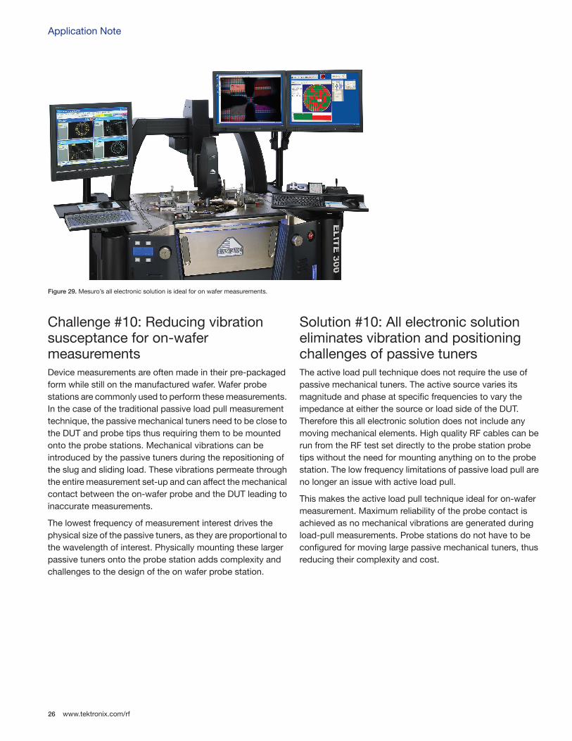
Challenge #10: Reducing vibration susceptance for on-wafer measurementsDevice measurements are often made in their pre-packaged form while still on the manufactured wafer. Wafer probe stations are commonly used to perform these measurements. In the case of the traditional passive load pull measurement technique, the passive mechanical tuners need to be close to the DUT and probe tips thus requiring them to be mounted onto the probe stations. Mechanical vibrations can be introduced by the passive tuners during the repositioning of the slug and sliding load. These vibrations permeate through the entire measurement set-up and can affect the mechanical contact between the on-wafer probe and the DUT leading to inaccurate measurements.
The lowest frequency of measurement interest drives the physical size of the passive tuners, as they are proportional to the wavelength of interest. Physically mounting these larger passive tuners onto the probe station adds complexity and challenges to the design of the on wafer probe station.
Solution #10: All electronic solution eliminates vibration and positioning challenges of passive tunersThe active load pull technique does not require the use of passive mechanical tuners. The active source varies its magnitude and phase at specific frequencies to vary the impedance at either the source or load side of the DUT. Therefore this all electronic solution does not include any moving mechanical elements. High quality RF cables can be run from the RF test set directly to the probe station probe tips without the need for mounting anything on to the probe station. The low frequency limitations of passive load pull are no longer an issue with active load pull.
This makes the active load pull technique ideal for on-wafer measurement. Maximum reliability of the probe contact is achieved as no mechanical vibrations are generated during load-pull measurements. Probe stations do not have to be configured for moving large passive mechanical tuners, thus reducing their complexity and cost.
Figure 29. Mesuro’s all electronic solution is ideal for on wafer measurements.

www.tektronix.com/rf 27
Overcoming Nonlinear Measurement Challenges
ConclusionThe strong demand for broadband power efficient wireless systems and the continued challenges that PA designers are facing in realizing them has created unique market openness for new solutions which in turn creates an opportunity for the establishment of new RF test & measurement solutions that are more appropriate for RF PA design.
Tektronix and Mesuro have teamed to offer a measurement solution that cuts down the characterization time through the simultaneous utilization of its waveform measurement and harmonic load pull capability. The advantage of this approach
is that it eliminates the need for systematic yet time consuming multi-dimensional parameter sweeps and enables the designer a more directed approach with the added benefit that the resulting device performance is close to a theoretical optimum. The solutions ability to simultaneously collect data at baseband, fundamental and harmonic frequencies enables designers to obtain maximum performance from a given technology. Its modular approach takes fully into account the diversity of the market spanning small, medium and large power applications offering solutions for markets operating up to 20W and 150W.
Application Note
www.tektronix.com/rf28
References1. J. Benedikt et al., “High Power Time Domain Measurement
System with Active Harmonic Load-pull for High Efficiency Base Station Amplifier Design,” IEEE MTT-S Int. Microwave Symp. Digest, June 2000, pp. 1459-1462.
2. A. Sheikh et al., “The Impact of System Impedance on the Characterization of High Power Devices,” Proceedings of the 37th European Microwave Conf., Oct 2007, pp. 949-952.
3. H. Qi, J. Benedikt, P. J. Tasker, “Nonlinear Data Utilization: from Direct Data Look-up to Behavioural Modeling,” to be published in IEEE Trans. Microwave Theory Tech. 2009.
4. H. Qi, J. Benedikt, P. J. Tasker, “Novel Nonlinear Model for Rapid Waveform-based Extraction Enabling Accurate High Power PA Design,” in 2007 IEEE MTT-S International Microwave Symposium Digest, Honolulu, Hawaii, USA, June 3-8, 2007.
5. H. Qi, J. Benedikt, and P. J. Tasker, “A novel approach for effective import of nonlinear device characteristics into CAD for large signal power amplifier design,” in 2006 IEEE MTT-S International Microwave Symposium Digest, San Francisco, CA, USA, June 11-16, 2006.
6. P. Wright, J. Lees, P. J. Tasker, J. Benedikt, S. C. Cripps, “An Efficient, Linear, Broadband Class-J-Mode PA Realised Using RF Waveform Engineering,” in 2009 IEEE MTT-S International Microwave Symposium Digest, Boston, Massachusetts, USA, June 7-12, 2009.
7. Cripps, S. C., “RF Power Amplifiers for Wireless Communications”, 2nd Edition, Artech House Publishers, 2006.
8. P. Wright, A. Sheikh, Ch. Roff, P. J. Tasker and J. Benedikt, “Highly Efficient Operation Modes in GaN Power Transistors Delivering Upwards of 81% Efficiency and 12W Output Power,” in 2008 IEEE MTT-S International Microwave Symposium Digest, Atlanta, Georgia, USA, June 15-20, 2008.
9. C. Roff, J. Benedikt, P.J. Tasker, D.J. Wallis, K.P. Hilton, J.O. Maclean, D.G. Hayes, M.J. Uren & T. Martin, “Utilization of Waveform Measurements for Degradation Analysis of AlGaN/GaN HFETs,” 70th ARFTG Microwave Measurement Symposium, Tempe, Arizona, USA, Nov 2007.
10. C. Roff, J. Benedikt, P. J. Tasker, and Mike Uren et al, “Analysis of DC-RF Dispersion in AlGaN/GaN HFETs using RF Waveform Engineering,” IEEE Transactions on Electron Devices, volume 56, issue 1, pp. 13-19, January 2009.
11. U.K. Mishra, P. Parikh and Y. Wu, “AlGaN/GaN HEMTs – an overview of device operation and applications,” Proceedings of the IEEE, volume 90, issue 6, June 2002, pp. 1022-1031.
12. J.L. Hudgins, G.S. Simin, E. Santi and M.A. Kahn, “An assessment of wide bandgap semiconductors for power devices,” IEEE Transactions on Power Electronics, volume 18, Issue 3, May 2003, pp. 907-914.
13. E. Piner, S. Singhal, P. Rajagopal, R. Therrien, J.C. Roberts, T. Li, A. W. Hanson, J. W. Johnson, I.C. Kizilyalli and K.J. Linthicum, “Device Degradation Phenomena in GaN HFET Technology: Status, Mechanisms and Opportunities,” IEEE International Electron Devices Meeting, 2006.
14. Y. Y. Woo, Y. Yang and B. Kim, “Analysis and Experiments for High-Efficiency Class-F and Inverse Class-F Power Amplifiers,” IEEE Trans. Microwave Theory & Tech., vol. 54, no. 5, pp. 1969-1974, May 2006.
15. Chris Roff, et al., “Detailed Analysis of DC-RF Dispersion in AlGaN/GaN HFETs using Waveform Measurements,” European Microwave Integrated Circuits Conference, 2006. The 1st , vol., no., pp.43-45, Sept. 2006.
16. J. Lees, et al., “Experimental gallium nitride microwave Doherty amplifier,” IEEE Electronic Letters, pp. 1284-1285, November 2005.
17. Raab, F.H., “Maximum efficiency and output of class-F power amplifiers,” Microwave Theory and Techniques, IEEE Transactions on , vol.49, no.6, pp.1162-1166, Jun 2001.


For Further InformationTektronix maintains a comprehensive, constantly expanding collection of application notes, technical briefs and other resources to help engineers working on the cutting edge of technology. Please visit www.tektronix.com
Copyright © 2010, Tektronix. All rights reserved. Tektronix products are covered by U.S. and foreign patents, issued and pending. Information in this publication supersedes that in all previously published material. Specification and price change privileges reserved. TEKTRONIX and TEK are registered trademarks of Tektronix, Inc. All other trade names referenced are the service marks, trademarks or registered trademarks of their respective companies. 7/2010 Internal/POD 37W-23395-1
Contact Tektronix:ASEAN / Australasia (65) 6356 3900
Austria* 00800 2255 4835
Balkans, Israel, South Africa and other ISE Countries +41 52 675 3777
Belgium* 00800 2255 4835
Brazil +55 (11) 3759 7600
Canada 1 (800) 833-9200
Central East Europe, Ukraine and the Baltics +41 52 675 3777
Central Europe & Greece +41 52 675 3777
Denmark +45 80 88 1401
Finland +41 52 675 3777
France* 00800 2255 4835
Germany* 00800 2255 4835
Hong Kong 400-820-5835
India 000-800-650-1835
Italy* 00800 2255 4835
Japan 81 (3) 6714-3010
Luxembourg +41 52 675 3777
Mexico, Central/South America & Caribbean 52 (55) 56 04 50 90
Middle East, Asia and North Africa +41 52 675 3777
The Netherlands* 00800 2255 4835
Norway 800 16098
People’s Republic of China 400-820-5835
Poland +41 52 675 3777
Portugal 80 08 12370
Republic of Korea 001-800-8255-2835
Russia & CIS +7 (495) 7484900
South Africa +27 11 206 8360
Spain* 00800 2255 4835
Sweden* 00800 2255 4835
Switzerland* 00800 2255 4835
Taiwan 886 (2) 2722-9622
United Kingdom & Ireland* 00800 2255 4835
USA 1 (800) 833-9200
* If the European phone number above is not accessible, please call +41 52 675 3777
Contact List Updated 25 May 2010


![MEASUREMENT ERRORS arXiv:math/0508600v1 [math.ST] 30 … · ESTIMATION OF NONLINEAR MODELS WITH BERKSON MEASUREMENT ERRORS1 By Liqun Wang UniversityofManitoba This paper is concerned](https://static.fdocuments.us/doc/165x107/5f085e617e708231d421aab5/measurement-errors-arxivmath0508600v1-mathst-30-estimation-of-nonlinear-models.jpg)


